CN101714546B - Display device and manufacturing method thereof - Google Patents
Display device and manufacturing method thereof Download PDFInfo
- Publication number
- CN101714546B CN101714546B CN200910175792.5A CN200910175792A CN101714546B CN 101714546 B CN101714546 B CN 101714546B CN 200910175792 A CN200910175792 A CN 200910175792A CN 101714546 B CN101714546 B CN 101714546B
- Authority
- CN
- China
- Prior art keywords
- wiring
- semiconductor layer
- gate
- thin film
- film transistor
- Prior art date
- Legal status (The legal status is an assumption and is not a legal conclusion. Google has not performed a legal analysis and makes no representation as to the accuracy of the status listed.)
- Active
Links
Images


Classifications
-
- G—PHYSICS
- G09—EDUCATION; CRYPTOGRAPHY; DISPLAY; ADVERTISING; SEALS
- G09G—ARRANGEMENTS OR CIRCUITS FOR CONTROL OF INDICATING DEVICES USING STATIC MEANS TO PRESENT VARIABLE INFORMATION
- G09G3/00—Control arrangements or circuits, of interest only in connection with visual indicators other than cathode-ray tubes
- G09G3/20—Control arrangements or circuits, of interest only in connection with visual indicators other than cathode-ray tubes for presentation of an assembly of a number of characters, e.g. a page, by composing the assembly by combination of individual elements arranged in a matrix no fixed position being assigned to or needed to be assigned to the individual characters or partial characters
- G09G3/22—Control arrangements or circuits, of interest only in connection with visual indicators other than cathode-ray tubes for presentation of an assembly of a number of characters, e.g. a page, by composing the assembly by combination of individual elements arranged in a matrix no fixed position being assigned to or needed to be assigned to the individual characters or partial characters using controlled light sources
- G09G3/30—Control arrangements or circuits, of interest only in connection with visual indicators other than cathode-ray tubes for presentation of an assembly of a number of characters, e.g. a page, by composing the assembly by combination of individual elements arranged in a matrix no fixed position being assigned to or needed to be assigned to the individual characters or partial characters using controlled light sources using electroluminescent panels
- G09G3/32—Control arrangements or circuits, of interest only in connection with visual indicators other than cathode-ray tubes for presentation of an assembly of a number of characters, e.g. a page, by composing the assembly by combination of individual elements arranged in a matrix no fixed position being assigned to or needed to be assigned to the individual characters or partial characters using controlled light sources using electroluminescent panels semiconductive, e.g. using light-emitting diodes [LED]
- G09G3/3208—Control arrangements or circuits, of interest only in connection with visual indicators other than cathode-ray tubes for presentation of an assembly of a number of characters, e.g. a page, by composing the assembly by combination of individual elements arranged in a matrix no fixed position being assigned to or needed to be assigned to the individual characters or partial characters using controlled light sources using electroluminescent panels semiconductive, e.g. using light-emitting diodes [LED] organic, e.g. using organic light-emitting diodes [OLED]
- G09G3/3225—Control arrangements or circuits, of interest only in connection with visual indicators other than cathode-ray tubes for presentation of an assembly of a number of characters, e.g. a page, by composing the assembly by combination of individual elements arranged in a matrix no fixed position being assigned to or needed to be assigned to the individual characters or partial characters using controlled light sources using electroluminescent panels semiconductive, e.g. using light-emitting diodes [LED] organic, e.g. using organic light-emitting diodes [OLED] using an active matrix
- G09G3/3233—Control arrangements or circuits, of interest only in connection with visual indicators other than cathode-ray tubes for presentation of an assembly of a number of characters, e.g. a page, by composing the assembly by combination of individual elements arranged in a matrix no fixed position being assigned to or needed to be assigned to the individual characters or partial characters using controlled light sources using electroluminescent panels semiconductive, e.g. using light-emitting diodes [LED] organic, e.g. using organic light-emitting diodes [OLED] using an active matrix with pixel circuitry controlling the current through the light-emitting element
-
- H—ELECTRICITY
- H10—SEMICONDUCTOR DEVICES; ELECTRIC SOLID-STATE DEVICES NOT OTHERWISE PROVIDED FOR
- H10D—INORGANIC ELECTRIC SEMICONDUCTOR DEVICES
- H10D30/00—Field-effect transistors [FET]
- H10D30/60—Insulated-gate field-effect transistors [IGFET]
- H10D30/67—Thin-film transistors [TFT]
- H10D30/6729—Thin-film transistors [TFT] characterised by the electrodes
- H10D30/6737—Thin-film transistors [TFT] characterised by the electrodes characterised by the electrode materials
- H10D30/6739—Conductor-insulator-semiconductor electrodes
-
- H—ELECTRICITY
- H10—SEMICONDUCTOR DEVICES; ELECTRIC SOLID-STATE DEVICES NOT OTHERWISE PROVIDED FOR
- H10D—INORGANIC ELECTRIC SEMICONDUCTOR DEVICES
- H10D62/00—Semiconductor bodies, or regions thereof, of devices having potential barriers
- H10D62/80—Semiconductor bodies, or regions thereof, of devices having potential barriers characterised by the materials
- H10D62/81—Semiconductor bodies, or regions thereof, of devices having potential barriers characterised by the materials of structures exhibiting quantum-confinement effects, e.g. single quantum wells; of structures having periodic or quasi-periodic potential variation
-
- H—ELECTRICITY
- H10—SEMICONDUCTOR DEVICES; ELECTRIC SOLID-STATE DEVICES NOT OTHERWISE PROVIDED FOR
- H10D—INORGANIC ELECTRIC SEMICONDUCTOR DEVICES
- H10D64/00—Electrodes of devices having potential barriers
- H10D64/60—Electrodes characterised by their materials
- H10D64/66—Electrodes having a conductor capacitively coupled to a semiconductor by an insulator, e.g. MIS electrodes
- H10D64/68—Electrodes having a conductor capacitively coupled to a semiconductor by an insulator, e.g. MIS electrodes characterised by the insulator, e.g. by the gate insulator
- H10D64/681—Electrodes having a conductor capacitively coupled to a semiconductor by an insulator, e.g. MIS electrodes characterised by the insulator, e.g. by the gate insulator having a compositional variation, e.g. multilayered
- H10D64/685—Electrodes having a conductor capacitively coupled to a semiconductor by an insulator, e.g. MIS electrodes characterised by the insulator, e.g. by the gate insulator having a compositional variation, e.g. multilayered being perpendicular to the channel plane
-
- H—ELECTRICITY
- H10—SEMICONDUCTOR DEVICES; ELECTRIC SOLID-STATE DEVICES NOT OTHERWISE PROVIDED FOR
- H10D—INORGANIC ELECTRIC SEMICONDUCTOR DEVICES
- H10D64/00—Electrodes of devices having potential barriers
- H10D64/60—Electrodes characterised by their materials
- H10D64/66—Electrodes having a conductor capacitively coupled to a semiconductor by an insulator, e.g. MIS electrodes
- H10D64/68—Electrodes having a conductor capacitively coupled to a semiconductor by an insulator, e.g. MIS electrodes characterised by the insulator, e.g. by the gate insulator
- H10D64/693—Electrodes having a conductor capacitively coupled to a semiconductor by an insulator, e.g. MIS electrodes characterised by the insulator, e.g. by the gate insulator the insulator comprising nitrogen, e.g. nitrides, oxynitrides or nitrogen-doped materials
-
- H—ELECTRICITY
- H10—SEMICONDUCTOR DEVICES; ELECTRIC SOLID-STATE DEVICES NOT OTHERWISE PROVIDED FOR
- H10D—INORGANIC ELECTRIC SEMICONDUCTOR DEVICES
- H10D86/00—Integrated devices formed in or on insulating or conducting substrates, e.g. formed in silicon-on-insulator [SOI] substrates or on stainless steel or glass substrates
- H10D86/01—Manufacture or treatment
- H10D86/021—Manufacture or treatment of multiple TFTs
-
- H—ELECTRICITY
- H10—SEMICONDUCTOR DEVICES; ELECTRIC SOLID-STATE DEVICES NOT OTHERWISE PROVIDED FOR
- H10D—INORGANIC ELECTRIC SEMICONDUCTOR DEVICES
- H10D86/00—Integrated devices formed in or on insulating or conducting substrates, e.g. formed in silicon-on-insulator [SOI] substrates or on stainless steel or glass substrates
- H10D86/40—Integrated devices formed in or on insulating or conducting substrates, e.g. formed in silicon-on-insulator [SOI] substrates or on stainless steel or glass substrates characterised by multiple TFTs
- H10D86/421—Integrated devices formed in or on insulating or conducting substrates, e.g. formed in silicon-on-insulator [SOI] substrates or on stainless steel or glass substrates characterised by multiple TFTs having a particular composition, shape or crystalline structure of the active layer
- H10D86/423—Integrated devices formed in or on insulating or conducting substrates, e.g. formed in silicon-on-insulator [SOI] substrates or on stainless steel or glass substrates characterised by multiple TFTs having a particular composition, shape or crystalline structure of the active layer comprising semiconductor materials not belonging to the Group IV, e.g. InGaZnO
-
- H—ELECTRICITY
- H10—SEMICONDUCTOR DEVICES; ELECTRIC SOLID-STATE DEVICES NOT OTHERWISE PROVIDED FOR
- H10D—INORGANIC ELECTRIC SEMICONDUCTOR DEVICES
- H10D86/00—Integrated devices formed in or on insulating or conducting substrates, e.g. formed in silicon-on-insulator [SOI] substrates or on stainless steel or glass substrates
- H10D86/40—Integrated devices formed in or on insulating or conducting substrates, e.g. formed in silicon-on-insulator [SOI] substrates or on stainless steel or glass substrates characterised by multiple TFTs
- H10D86/441—Interconnections, e.g. scanning lines
-
- H—ELECTRICITY
- H10—SEMICONDUCTOR DEVICES; ELECTRIC SOLID-STATE DEVICES NOT OTHERWISE PROVIDED FOR
- H10D—INORGANIC ELECTRIC SEMICONDUCTOR DEVICES
- H10D86/00—Integrated devices formed in or on insulating or conducting substrates, e.g. formed in silicon-on-insulator [SOI] substrates or on stainless steel or glass substrates
- H10D86/40—Integrated devices formed in or on insulating or conducting substrates, e.g. formed in silicon-on-insulator [SOI] substrates or on stainless steel or glass substrates characterised by multiple TFTs
- H10D86/60—Integrated devices formed in or on insulating or conducting substrates, e.g. formed in silicon-on-insulator [SOI] substrates or on stainless steel or glass substrates characterised by multiple TFTs wherein the TFTs are in active matrices
-
- H10P14/3434—
-
- G—PHYSICS
- G09—EDUCATION; CRYPTOGRAPHY; DISPLAY; ADVERTISING; SEALS
- G09G—ARRANGEMENTS OR CIRCUITS FOR CONTROL OF INDICATING DEVICES USING STATIC MEANS TO PRESENT VARIABLE INFORMATION
- G09G2310/00—Command of the display device
- G09G2310/02—Addressing, scanning or driving the display screen or processing steps related thereto
- G09G2310/0264—Details of driving circuits
- G09G2310/0286—Details of a shift registers arranged for use in a driving circuit
-
- G—PHYSICS
- G09—EDUCATION; CRYPTOGRAPHY; DISPLAY; ADVERTISING; SEALS
- G09G—ARRANGEMENTS OR CIRCUITS FOR CONTROL OF INDICATING DEVICES USING STATIC MEANS TO PRESENT VARIABLE INFORMATION
- G09G2310/00—Command of the display device
- G09G2310/02—Addressing, scanning or driving the display screen or processing steps related thereto
- G09G2310/0264—Details of driving circuits
- G09G2310/0297—Special arrangements with multiplexing or demultiplexing of display data in the drivers for data electrodes, in a pre-processing circuitry delivering display data to said drivers or in the matrix panel, e.g. multiplexing plural data signals to one D/A converter or demultiplexing the D/A converter output to multiple columns
Landscapes
- Engineering & Computer Science (AREA)
- Computer Hardware Design (AREA)
- General Physics & Mathematics (AREA)
- Physics & Mathematics (AREA)
- Theoretical Computer Science (AREA)
- Thin Film Transistor (AREA)
- Liquid Crystal (AREA)
- Electroluminescent Light Sources (AREA)
- Metal-Oxide And Bipolar Metal-Oxide Semiconductor Integrated Circuits (AREA)
- Manufacturing & Machinery (AREA)
- Electrodes Of Semiconductors (AREA)
- Internal Circuitry In Semiconductor Integrated Circuit Devices (AREA)
- Power Engineering (AREA)
- Microelectronics & Electronic Packaging (AREA)
- Condensed Matter Physics & Semiconductors (AREA)
- Physical Vapour Deposition (AREA)
- Devices For Indicating Variable Information By Combining Individual Elements (AREA)
- Shift Register Type Memory (AREA)
Abstract
Description
技术领域 technical field
本发明涉及使用氧化物半导体的显示装置及其制造方法。The present invention relates to a display device using an oxide semiconductor and a method of manufacturing the same.
背景技术 Background technique
如以液晶显示装置为代表那样,形成在玻璃衬底等的平板的薄膜晶体管由非晶硅、多晶硅制造。使用非晶硅的薄膜晶体管具有如下特征:虽然其电场效应迁移率低,但是可以对应于玻璃衬底的大面积化。另一方面,使用结晶硅的薄膜晶体管具有如下特征:虽然其电场效应迁移率高,但是需要激光退火等的晶化工序,且不一定适用于玻璃衬底的大面积化。A thin film transistor formed on a flat plate such as a glass substrate, as typified by a liquid crystal display device, is made of amorphous silicon or polycrystalline silicon. A thin film transistor using amorphous silicon has a feature that it can cope with a larger area of a glass substrate, although its electric field effect mobility is low. On the other hand, thin film transistors using crystalline silicon are characterized in that they require a crystallization process such as laser annealing, although they have high field-effect mobility, and are not necessarily suitable for large-area glass substrates.
针对于此,使用氧化物半导体制造薄膜晶体管,并应用于电子器件及光器件的技术引人注目。例如,专利文献1及专利文献2公开使用氧化锌、In-Ga-Zn-O类氧化物半导体用作氧化物半导体膜制造薄膜晶体管,并将它用作图像显示装置的开关元件等的技术。In view of this, the technology of manufacturing thin film transistors using oxide semiconductors and applying them to electronic devices and optical devices is attracting attention. For example,
[专利文献1]日本专利申请公开2007-123861号公报[Patent Document 1] Japanese Patent Application Publication No. 2007-123861
[专利文献2]日本专利申请公开2007-096055号公报[Patent Document 2] Japanese Patent Application Publication No. 2007-096055
在氧化物半导体设置沟道形成区的薄膜晶体管可以获得比使用非晶硅的薄膜晶体管高的电场效应迁移率。可以通过溅射法等以300℃以下形成氧化物半导体膜,其制造工序与使用多晶硅的薄膜晶体管的制造工序相比简单。A thin film transistor in which a channel formation region is provided in an oxide semiconductor can obtain higher electric field effect mobility than a thin film transistor using amorphous silicon. The oxide semiconductor film can be formed by sputtering or the like at a temperature of 300° C. or lower, and its manufacturing process is simpler than that of a thin film transistor using polysilicon.
期望使用这种氧化物半导体在玻璃衬底、塑料衬底等形成薄膜晶体管,并将它应用于液晶显示器、电致发光显示器或电子纸等的显示装置。It is desired to form a thin film transistor on a glass substrate, a plastic substrate, or the like using such an oxide semiconductor, and to apply it to a display device such as a liquid crystal display, an electroluminescent display, or electronic paper.
随着显示装置的高精细化,像素数增加,并且栅极数及信号线数也增加。当栅极数及信号线数增加时,不容易通过键合等安装包括用来驱动它们的驱动电路的IC芯片,因此制造成本增高。With the high definition of display devices, the number of pixels increases, and the number of gates and signal lines also increase. When the number of gates and the number of signal lines increase, it is not easy to mount IC chips including a driving circuit for driving them by bonding or the like, and thus the manufacturing cost increases.
发明内容 Contents of the invention
于是,本发明的实施方式之一的目的在于将氧化物半导体用于驱动像素部的驱动电路的至少一部分来减少制造成本。Therefore, an object of an embodiment of the present invention is to reduce manufacturing costs by using an oxide semiconductor for at least a part of a driver circuit for driving a pixel portion.
此外,本发明的实施方式之一的目的还在于在驱动电路中减少连接元件的布线之间的接触电阻等,以谋求高速驱动。例如,当栅极布线和上层布线的接触电阻高时,有在被输入的信号中产生应变的忧虑。In addition, an object of an embodiment of the present invention is to reduce contact resistance and the like between wirings connecting elements in a drive circuit to achieve high-speed driving. For example, when the contact resistance between the gate wiring and the upper layer wiring is high, strain may be generated in an input signal.
此外,本发明的实施方式之一的目的还在于提供可以减少接触孔数并缩小驱动电路的占有面积的显示装置的结构。In addition, an object of one embodiment of the present invention is to provide a structure of a display device capable of reducing the number of contact holes and reducing the occupied area of a driving circuit.
在本发明的实施方式之一中,在同一衬底上由使用氧化物半导体的薄膜晶体管构成像素部和驱动像素部的驱动电路的至少一部分的电路。通过在同一衬底上设置像素部和驱动电路,减少制造成本。In one of the embodiments of the present invention, the pixel portion and at least a part of a circuit for driving the pixel portion are formed of a thin film transistor using an oxide semiconductor on the same substrate. Manufacturing cost is reduced by providing a pixel portion and a driver circuit on the same substrate.
在本说明书中使用的氧化物半导体形成表示为InMO3(ZnO)m(m>0)的薄膜,并制造将该薄膜用作半导体层的薄膜晶体管。另外,M表示选自Ga(镓)、Fe(铁)、Ni(镍)、Mn(锰)及Co(钴)中的一种金属元素或多种金属元素。例如,作为M,有时采用Ga,有时包含Ga以外的上述金属元素诸如Ga和Ni或Ga和Fe等。此外,在上述氧化物半导体中,有不仅包含作为M的金属元素,而且还包含作为杂质元素的Fe、Ni等其他迁移金属元素或该迁移金属的氧化物的氧化物半导体。在本说明书中,也将该薄膜称为In-Ga-Zn-O类非单晶膜。The oxide semiconductor used in this specification forms a thin film expressed as InMO 3 (ZnO) m (m>0), and a thin film transistor using this thin film as a semiconductor layer is manufactured. In addition, M represents one or more metal elements selected from Ga (gallium), Fe (iron), Ni (nickel), Mn (manganese), and Co (cobalt). For example, as M, Ga is sometimes used, and the above-mentioned metal elements other than Ga such as Ga and Ni or Ga and Fe are sometimes contained. In addition, among the above-mentioned oxide semiconductors, there are oxide semiconductors containing not only the metal element as M but also other transition metal elements such as Fe and Ni as impurity elements or oxides of the transition metals. In this specification, this thin film is also referred to as an In-Ga-Zn-O-based non-single crystal film.
表1示出利用ICP-MS(Inductively Coupled Plasma MassSpectrometry:感应耦合等离子体质量分析法)的分析的典型测量例子。在使用In2O3∶Ga2O3∶ZnO=1∶1∶1的靶材(In∶Ga∶Zn=1∶1∶0.5),并在将进行溅射法时的氩气体流量设定为40sccm的条件1下可获得的氧化物半导体膜是InGa0.95Zn0.41O3.33。此外,在将进行溅射法时的氩气体流量设定为10sccm,氧流量设定为5sccm的条件2下可获得的氧化物半导体膜是InG0.94Zn0.40O3.31。Table 1 shows typical measurement examples of analysis by ICP-MS (Inductively Coupled Plasma Mass Spectrometry: Inductively Coupled Plasma Mass Spectrometry). When using a target of In 2 O 3 : Ga 2 O 3 : ZnO = 1: 1: 1 (In: Ga: Zn = 1: 1: 0.5), and setting the argon gas flow rate when performing the sputtering method The oxide semiconductor film obtainable under
[表1][Table 1]
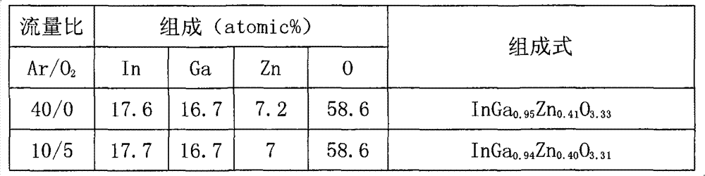
此外,表2示出将测量方法变为RBS(Rutherford BackscatteringSpectrometry:卢瑟福背散射光谱学法)进行定量化而得到的结果。In addition, Table 2 shows the results of quantification by changing the measurement method to RBS (Rutherford Backscattering Spectrometry: Rutherford Backscattering Spectrometry).
[表2][Table 2]

利用RBS分析测量条件1的样品。其结果是,氧化物半导体膜是InGa0.93Zn0.44O3.49。此外,利用RBS分析测量条件2的样品。其结果是,氧化物半导体膜是InGa0.92Zn0.45O3.86。The samples of
当进行XRD(X线衍射)测量时,在In-Ga-Zn-O类非单晶膜中观察到非晶结构。另外,通过溅射法形成测量的样品的In-Ga-Zn-O类非单晶膜之后,对它以200℃至500℃,典型地以300℃至400℃进行10分至100分的加热处理。此外,可以制造具有如下电特性的薄膜晶体管:当栅电压是±20V时,导通截止比是109以上,迁移率是10以上。When XRD (X-ray Diffraction) measurement was performed, an amorphous structure was observed in the In-Ga-Zn-O-based non-single crystal film. In addition, after the In-Ga-Zn-O-based non-single crystal film of the sample to be measured is formed by sputtering, it is heated at 200°C to 500°C, typically 300°C to 400°C, for 10 minutes to 100 minutes deal with. In addition, it is possible to manufacture a thin film transistor having electrical characteristics such that the on-off ratio is 10 9 or more and the mobility is 10 or more when the gate voltage is ±20 V.
将具有这种电特性的薄膜晶体管用于驱动电路是有效的。例如,栅极线驱动电路由按顺序传送栅极信号的移位寄存器电路、缓冲电路等构成,而源极线驱动电路由按顺序传送栅极信号的移位寄存器电路、缓冲电路、切换向像素传送影像信号的导通截止的模拟开关等构成。其迁移率比使用非晶硅的TFT的迁移率高的使用氧化物半导体膜的TFT可以使移位寄存器电路进行高速驱动。It is effective to use a thin film transistor having such electrical characteristics for a driving circuit. For example, the gate line driving circuit is composed of a shift register circuit, a buffer circuit, etc. that sequentially transmit gate signals, and the source line driving circuit is composed of a shift register circuit that sequentially transmits gate signals, a buffer circuit, switching to the pixel Consists of an analog switch that transmits video signals on and off. A TFT using an oxide semiconductor film whose mobility is higher than that of a TFT using amorphous silicon can drive a shift register circuit at high speed.
此外,在由使用氧化物半导体的薄膜晶体管构成驱动像素部的驱动电路的至少一部分的电路的情况下,都由n沟道型TFT形成,并且以图1B所示的电路为基本单位而形成。另外,在驱动电路中,通过使栅电极和源极布线或漏极布线直接连接,可以获得良好的接触,并减少接触电阻。当在驱动电路中通过其他导电膜,例如透明导电膜连接栅电极和源极布线或漏极布线时,有引起如下现象的忧虑:接触孔数的增加、接触孔数的增加所引起的占有面积的增大或接触电阻及布线电阻的增大、以及工序的复杂化。Also, when at least a part of the driver circuit for driving the pixel portion is formed of thin film transistors using oxide semiconductors, they are all formed of n-channel TFTs and formed using the circuit shown in FIG. 1B as a basic unit. In addition, in the drive circuit, by directly connecting the gate electrode and the source wiring or the drain wiring, good contact can be obtained and contact resistance can be reduced. When connecting the gate electrode and the source wiring or the drain wiring through other conductive films, such as transparent conductive films, in the drive circuit, there are concerns about the following phenomena: increase in the number of contact holes, increase in the occupied area due to the increase in the number of contact holes increase or increase in contact resistance and wiring resistance, and complicate the process.
本说明书所公开的发明结构是一种显示装置,包括像素部以及驱动电路,其中,像素部至少包括具有第一氧化物半导体层的第一薄膜晶体管,驱动电路至少包括具有第二氧化物半导体层的第二薄膜晶体管以及具有第三氧化物半导体层的第三薄膜晶体管,与设置在第二氧化物半导体层的下方的第二薄膜晶体管的栅电极直接接触的布线是与第三氧化物半导体层电连接的第三薄膜晶体管的源极布线或漏极布线,并且第三氧化物半导体层直接接触于布线上。The inventive structure disclosed in this specification is a display device including a pixel portion and a drive circuit, wherein the pixel portion includes at least a first thin film transistor having a first oxide semiconductor layer, and the drive circuit includes at least a second oxide semiconductor layer. The second thin film transistor and the third thin film transistor having the third oxide semiconductor layer, the wiring directly in contact with the gate electrode of the second thin film transistor disposed below the second oxide semiconductor layer is connected to the third oxide semiconductor layer The source wiring or the drain wiring of the third thin film transistor is electrically connected, and the third oxide semiconductor layer is directly in contact with the wiring.
本发明的实施方式之一解决上述课题中的至少一个。One embodiment of the present invention solves at least one of the above-mentioned problems.
此外,在上述结构中,第二薄膜晶体管的栅电极通过形成在覆盖栅电极的栅极绝缘层的接触孔与布线电连接。另外,在上述结构中,通过将像素部和驱动电路设置在同一衬底上,减少制造成本。Furthermore, in the above structure, the gate electrode of the second thin film transistor is electrically connected to the wiring through the contact hole formed in the gate insulating layer covering the gate electrode. In addition, in the above structure, the manufacturing cost is reduced by providing the pixel portion and the driving circuit on the same substrate.
此外,由于薄膜晶体管因静电等而容易损坏,因此优选对于栅极线或源极线将驱动电路保护用保护电路设置在同一衬底上。优选由使用氧化物半导体的非线性元件构成保护电路。In addition, since the thin film transistor is easily damaged by static electricity or the like, it is preferable to provide a protection circuit for driving circuit protection on the same substrate as the gate line or the source line. Preferably, the protection circuit is constituted by a nonlinear element using an oxide semiconductor.
此外,作为具有驱动电路的显示装置,除了液晶显示装置之外,还可以举出使用发光元件的发光显示装置以及使用电泳显示元件的也被称为电子纸的显示装置。In addition, as a display device having a driving circuit, in addition to a liquid crystal display device, a light-emitting display device using a light-emitting element and a display device also called electronic paper using an electrophoretic display element can be mentioned.
在使用发光元件的发光显示装置中,像素部具有多个薄膜晶体管,并且在像素部中也具有使某个薄膜晶体管的栅电极和其他晶体管的源极布线或漏极布线直接连接的部分。另外,在使用发光元件的发光显示装置的驱动电路中具有使薄膜晶体管的栅电极和该薄膜晶体管的源极布线或漏极布线直接连接的部分。In a light-emitting display device using a light-emitting element, a pixel portion includes a plurality of thin film transistors, and the pixel portion also has a portion where a gate electrode of a certain thin film transistor is directly connected to a source wiring or a drain wiring of another transistor. In addition, a drive circuit of a light-emitting display device using a light-emitting element has a portion in which a gate electrode of a thin film transistor is directly connected to a source wiring or a drain wiring of the thin-film transistor.
此外,制造方法也是本发明的实施方式之一,该结构是如下:在衬底上形成第一栅电极及第二栅电极;形成覆盖第一栅电极及第二栅电极的栅极绝缘层;对栅极绝缘层选择性地进行蚀刻来形成到达第二栅电极的接触孔;形成通过接触孔与第二栅电极直接接触的第一布线及隔着第一栅极绝缘层与第一栅电极及第二栅电极的双方重叠的第二布线;以及在栅极绝缘层上形成与第一栅电极重叠的第一氧化物半导体层,且在栅极绝缘层上形成与第二栅电极重叠的第二氧化物半导体层,其中,第二氧化物半导体层接触于第一布线上及第二布线上。根据上述制造方法的结构,可以制造作为驱动电路的基本单位的反相器电路。In addition, the manufacturing method is also one of the embodiments of the present invention, and the structure is as follows: forming a first gate electrode and a second gate electrode on a substrate; forming a gate insulating layer covering the first gate electrode and the second gate electrode; The gate insulating layer is selectively etched to form a contact hole reaching the second gate electrode; forming a first wiring directly in contact with the second gate electrode through the contact hole and connecting the first gate electrode with the first gate insulating layer and a second wiring overlapping both of the second gate electrode; and forming a first oxide semiconductor layer overlapping the first gate electrode on the gate insulating layer, and forming a wiring overlapping the second gate electrode on the gate insulating layer A second oxide semiconductor layer, wherein the second oxide semiconductor layer is in contact with the first wiring and the second wiring. According to the configuration of the above-described manufacturing method, an inverter circuit that is a basic unit of a drive circuit can be manufactured.
当然,除了驱动电路之外,还可以将像素部的薄膜晶体管制造在同一衬底上。Of course, in addition to the driver circuit, thin film transistors in the pixel portion may also be fabricated on the same substrate.
此外,在上述制造工序中,优选通过在形成第一氧化物半导体层及第二氧化物半导体层之前,对栅极绝缘层表面进行等离子体处理,具体地说,进行反溅射,来去除表面的尘屑等。另外,优选在形成第一布线及第二布线之前对露出在栅极绝缘层表面及接触孔底面的第二栅电极表面进行等离子体处理,具体地说,进行反溅射,来去除表面的尘屑等。In addition, in the above-mentioned manufacturing process, it is preferable to perform plasma treatment on the surface of the gate insulating layer before forming the first oxide semiconductor layer and the second oxide semiconductor layer, specifically, perform reverse sputtering to remove the surface. dust, etc. In addition, before forming the first wiring and the second wiring, the surface of the second gate electrode exposed on the surface of the gate insulating layer and the bottom surface of the contact hole is preferably subjected to plasma treatment, specifically, reverse sputtering, to remove dust on the surface. Crumbs etc.
注意,从方便起见附加了第一、第二等序数词,因此其并不表示特定发明的工序顺序或层叠顺序。Note that ordinal numerals such as first and second are added for convenience, so they do not indicate the order of steps or the order of lamination of a particular invention.
通过在栅极线驱动电路或源极线驱动电路中使用氧化物半导体的薄膜晶体管,减少制造成本。而且,可以提供一种显示装置,其中通过使用于驱动电路的薄膜晶体管的栅电极和源极布线或漏极布线直接连接,可以减少接触孔数并缩小驱动电路的占有面积。Manufacturing cost is reduced by using a thin film transistor of an oxide semiconductor in a gate line driver circuit or a source line driver circuit. Furthermore, it is possible to provide a display device in which the number of contact holes can be reduced and the occupied area of the driving circuit can be reduced by directly connecting the gate electrode of the thin film transistor used in the driving circuit to the source wiring or the drain wiring.
附图说明 Description of drawings
图1A是本发明的实施方式之一的半导体装置的截面图,图1B是等效电路图,图1C是俯视图;FIG. 1A is a cross-sectional view of a semiconductor device according to one embodiment of the present invention, FIG. 1B is an equivalent circuit diagram, and FIG. 1C is a top view;
图2A是本发明的实施方式之一的半导体装置的等效电路图,图2B是俯视图;FIG. 2A is an equivalent circuit diagram of a semiconductor device according to one embodiment of the present invention, and FIG. 2B is a top view;
图3A至3C是本发明的实施方式之一的半导体装置的工序截面图;3A to 3C are process sectional views of a semiconductor device according to one embodiment of the present invention;
图4A至4C是本发明的实施方式之一的半导体装置的工序截面图;4A to 4C are process sectional views of a semiconductor device according to one embodiment of the present invention;
图5A至5C是本发明的实施方式之一的半导体装置的工序截面图;5A to 5C are process sectional views of a semiconductor device according to one embodiment of the present invention;
图6是本发明的实施方式之一的半导体装置的俯视图;6 is a top view of a semiconductor device according to one embodiment of the present invention;
图7是本发明的实施方式之一的半导体装置的俯视图;7 is a top view of a semiconductor device according to one embodiment of the present invention;
图8是本发明的实施方式之一的半导体装置的俯视图;8 is a top view of a semiconductor device according to one embodiment of the present invention;
图9是本发明的实施方式之一的半导体装置的俯视图;9 is a top view of a semiconductor device according to one embodiment of the present invention;
图10A至10D是本发明的实施方式之一的半导体装置的端子部的俯视图及截面图;10A to 10D are plan views and cross-sectional views of a terminal portion of a semiconductor device according to one embodiment of the present invention;
图11是本发明的实施方式之一的半导体装置的像素俯视图;11 is a top view of a pixel of a semiconductor device according to one embodiment of the present invention;
图12是电子纸的截面图;12 is a cross-sectional view of electronic paper;
图13A和13B是说明半导体装置的框图的图;13A and 13B are diagrams illustrating a block diagram of a semiconductor device;
图14是说明源极线驱动电路的结构的图;FIG. 14 is a diagram illustrating a structure of a source line driving circuit;
图15是说明源极线驱动电路的工作的时序图;FIG. 15 is a timing chart illustrating the operation of the source line driving circuit;
图16是说明源极线驱动电路的工作的时序图;FIG. 16 is a timing chart illustrating the operation of the source line driving circuit;
图17是说明移位寄存器的结构的图;FIG. 17 is a diagram illustrating the structure of a shift register;
图18是说明图17所示的触发器的连接结构的图;FIG. 18 is a diagram illustrating the connection structure of the flip-flop shown in FIG. 17;
图19A至19C是说明本发明的实施方式之一的半导体装置的俯视图及截面图;19A to 19C are plan views and cross-sectional views illustrating a semiconductor device according to one embodiment of the present invention;
图20是说明本发明的实施方式之一的半导体装置的截面图;20 is a cross-sectional view illustrating a semiconductor device according to one embodiment of the present invention;
图21是说明本发明的实施方式之一的半导体装置的像素等效电路的图;21 is a diagram illustrating a pixel equivalent circuit of a semiconductor device according to one embodiment of the present invention;
图22A至22C是说明本发明的实施方式之一的半导体装置的图;22A to 22C are diagrams illustrating a semiconductor device according to one embodiment of the present invention;
图23A和23B是说明本发明的实施方式之一的半导体装置的俯视图及截面图;23A and 23B are a plan view and a cross-sectional view illustrating a semiconductor device according to one embodiment of the present invention;
图24A和24B是说明电子纸的使用方式的例子的图;24A and 24B are diagrams illustrating examples of ways of using electronic paper;
图25是示出电子书籍的一例的外观图;FIG. 25 is an external view showing an example of an electronic book;
图26A和26B是示出电视装置及数码相框的例子的外观图;26A and 26B are external views showing examples of a television set and a digital photo frame;
图27A和27B是示出游戏机的例子的外观图;27A and 27B are external views showing examples of gaming machines;
图28A和28B是示出移动电话机的一例的外观图;28A and 28B are external views showing an example of a mobile phone;
图29是示出作为TFT的电特性的VG-ID曲线的图;FIG. 29 is a graph showing a V G -ID curve as an electrical characteristic of a TFT;
图30是示出表示移位寄存器的第44级、第43级及第42级的输出波形的利用示波器的测量结果的图;FIG. 30 is a diagram showing measurement results with an oscilloscope showing the output waveforms of the 44th, 43rd, and 42nd stages of the shift register;
图31是示出表示最大驱动频率时的驱动器输出波形的利用示波器的测量结果的图;Fig. 31 is a diagram showing the measurement results using an oscilloscope representing the driver output waveform at the time of the maximum driving frequency;
图32是示出液晶显示器的显示的状态的图。FIG. 32 is a diagram showing a display state of a liquid crystal display.
具体实施方式 Detailed ways
下面,说明本发明的实施方式。Next, embodiments of the present invention will be described.
实施方式1
在此,根据使用两个n沟道型薄膜晶体管构成反相器电路的例子,以下说明本发明的实施方式之一。Here, one embodiment of the present invention will be described below based on an example in which an inverter circuit is configured using two n-channel thin film transistors.
使用反相器电路、电容、电阻等构成用来驱动像素部的驱动电路。有组合两个n沟道型TFT形成反相器电路的情况、组合增强型晶体管和耗尽型晶体管形成反相器电路的情况(下面称为EDMOS电路)、使用增强型TFT形成反相器电路的情况(下面称为EEMOS电路)。注意,在n沟道型TFT的阈值电压是正的情况下,定义为增强型晶体管,而在n沟道型TFT的阈值电压是负的情况下,定义为耗尽型晶体管。在本说明书中按照该定义进行描述。A drive circuit for driving the pixel portion is configured using an inverter circuit, capacitors, resistors, and the like. There are cases where two n-channel TFTs are combined to form an inverter circuit, where an enhancement type transistor and a depletion type transistor are combined to form an inverter circuit (hereinafter referred to as EDMOS circuit), and where an enhancement type TFT is used to form an inverter circuit The situation (hereinafter referred to as EEMOS circuit). Note that when the threshold voltage of the n-channel type TFT is positive, it is defined as an enhancement type transistor, and when the threshold voltage of the n-channel type TFT is negative, it is defined as a depletion type transistor. In this specification, description will be made according to this definition.
将像素部和驱动电路形成在同一衬底上,并且在像素部中,使用配置为矩阵状的增强型晶体管切换对像素电极的电压施加的导通截止。这种配置在像素部的增强型晶体管使用氧化物半导体,在其电特性中,当栅电压是±20V时,导通截止比是109以上,所以泄漏电流少且可以实现低耗电量驱动。The pixel portion and the driver circuit are formed over the same substrate, and in the pixel portion, voltage application to the pixel electrodes is switched on and off using enhancement transistors arranged in a matrix. This type of enhancement transistor placed in the pixel portion uses an oxide semiconductor. Among its electrical characteristics, when the gate voltage is ±20V, the on-off ratio is 10 9 or more, so the leakage current is small and low power consumption driving can be realized. .
图1A示出驱动电路的反相器电路的截面结构。在图1A中,在衬底400上设置第一栅电极401及第二栅电极402。可以使用钼、钛、铬、钽、钨、铝、铜、钕、钪等的金属材料或以这些材料为主要成分的合金材料,以它们的单层或叠层形成第一栅电极401及第二栅电极402。FIG. 1A shows a cross-sectional structure of an inverter circuit of a driving circuit. In FIG. 1A , a
例如,作为第一栅电极401及第二栅电极402的两层的叠层结构,优选采用在铝层上层叠钼层的两层结构、在铜层上层叠钼层的两层结构、在铜层上层叠氮化钛层或氮化钽层的两层结构、层叠氮化钛层和钼层的两层结构。作为三层的叠层结构,优选采用钨层或氮化钨、铝和硅的合金或铝和钛的合金、氮化钛或钛层的叠层。For example, as the two-layer laminated structure of the
此外,在覆盖第一栅电极401及第二栅电极402的栅极绝缘层403上设置第一布线409、第二布线410及第三布线411,并且在第二布线410通过形成在栅极绝缘层403的接触孔404与第二栅电极402直接连接。In addition, the
此外,在与第一栅电极401重叠的位置设置接触于第一布线409及第二布线410上的第一氧化物半导体层405,且在与第二栅电极402重叠的位置设置接触于第二布线410及第三布线411上的第二氧化物半导体层407。另外,优选在形成第一氧化物半导体层405或第二氧化物半导体层407之前,对栅极绝缘层403的表面进行等离子体处理。例如,优选通过在采用溅射法形成氧化物半导体膜之前进行引入氩气体来产生等离子体的反溅射,去除附着到栅极绝缘层403的表面及接触孔404的底面的尘屑。反溅射是指一种方法,其中不对靶材一侧施加电压而在氩气氛下使用RF电源对衬底一侧施加电压来在衬底形成等离子体,从而对表面进行改性。另外,也可以使用氮、氦等代替氩气氛。此外,也可以在对氩气氛添加氧、氢、N2O等的气氛下进行反溅射。另外,也可以在对氩气氛添加Cl2、CF4等的气氛下进行反溅射。In addition, the first
第一薄膜晶体管430具有第一栅电极401和隔着栅极绝缘层403与第一栅电极401重叠的第一氧化物半导体层405,并且第一布线409是接地电位的电源线(接地电源线)。该接地电位的电源线也可以是被施加负电压VDL的电源线(负电源线)。The first
此外,第二薄膜晶体管431具有第二栅电极402和隔着栅极绝缘层403与第二栅电极402重叠的第二氧化物半导体层407,并且第三布线411是被施加正电压VDD的电源线(正电源线)。Further, the second
如图1A所示那样,电连接到第一氧化物半导体层405和第二氧化物半导体层407的双方的第二布线410通过形成在栅极绝缘层403的接触孔404与第二薄膜晶体管431的第二栅电极402直接连接。通过使第二布线410和第二栅电极402直接连接,可以获得良好的接触并减少接触电阻。与隔着其他导电膜,例如透明导电膜连接第二栅电极402和第二布线410的情况相比,可以谋求接触孔数的减少、借助于接触孔数的减少的占有面积的缩小。As shown in FIG. 1A, the
此外,图1C示出驱动电路的反相器电路的俯视图。在图1C中,沿着虚线Z1-Z2截断的截面对应于图1A。Furthermore, FIG. 1C shows a top view of the inverter circuit of the driving circuit. In FIG. 1C , a section taken along the dotted line Z1 - Z2 corresponds to FIG. 1A .
另外,图1B示出EDMOS电路的等效电路。图1A及图1C所示的电路连接相当于图1B,并且它是第一薄膜晶体管430是增强型n沟道型晶体管,而第二薄膜晶体管431是耗尽型n沟道型晶体管的例子。In addition, FIG. 1B shows an equivalent circuit of an EDMOS circuit. The circuit connection shown in FIG. 1A and FIG. 1C is equivalent to FIG. 1B, and it is an example in which the first
作为在同一衬底上制造增强型n沟道型晶体管和耗尽型n沟道型晶体管的方法,例如使用不同的材料及不同的成膜条件制造第一氧化物半导体层405和第二氧化物半导体层407。此外,也可以在氧化物半导体层的上下设置栅电极控制阈值,对栅电极施加电压以使得一方TFT成为常导通状态(normally-on),并使得另一方TFT成为常截止状态(normally-off)而构成EDMOS电路。As a method of manufacturing an enhancement-type n-channel transistor and a depletion-type n-channel transistor on the same substrate, for example, the first
实施方式2
实施方式1示出EDMOS电路的例子。在本实施方式中,图2A示出EEMOS电路的等效电路。在图2A的等效电路中,既可以采用两个都是增强型n沟道型晶体管的组合,又可以采用第一薄膜晶体管460是增强型n沟道型晶体管,而另一方晶体管的第二薄膜晶体管461是耗尽型n沟道型晶体管的组合。通过采用上述组合中任一个都可以制造驱动电路。
当将可采用两个都是相同的增强型n沟道型晶体管的组合制造的图2A的电路结构用于驱动电路时,用于像素部的晶体管也是相同的增强型n沟道型晶体管,所以制造工序不增大,因此可以说是优选的。此外,图2B示出俯视图。When the circuit structure of FIG. 2A, which can be manufactured using a combination of two identical enhancement n-channel transistors, is used for the driving circuit, the transistors used for the pixel portion are also the same enhancement n-channel transistors, so It can be said that it is preferable since the manufacturing process does not increase. In addition, FIG. 2B shows a plan view.
此外,图3A、图3B及图3C示出反相器电路的制造工序的一例。另外,沿着图2B中的虚线Y1-Y2截断的截面相当于图3C。In addition, FIG. 3A, FIG. 3B, and FIG. 3C show an example of the manufacturing process of the inverter circuit. In addition, a cross section taken along the dotted line Y1 - Y2 in FIG. 2B corresponds to FIG. 3C .
在衬底440上通过溅射法形成第一导电膜,使用第一光掩模对第一导电膜选择性地进行蚀刻,形成第一栅电极441及第二栅电极442。接着,采用等离子体CVD法或溅射法形成覆盖第一栅电极441及第二栅电极442的栅极绝缘层443。可以采用CVD法或溅射法等使用氧化硅层、氮化硅层、氧氮化硅层或氮氧化硅层的单层或叠层形成栅极绝缘层443。此外,作为栅极绝缘层443,也可以采用使用有机硅烷气体的CVD法形成氧化硅层。作为有机硅烷气体,可以使用含硅化合物诸如正硅酸乙酯(TEOS:化学式Si(OC2H5)4)、四甲基硅烷(TMS:化学式Si(CH3)4)、四甲基环四硅氧烷(TMCTS)、八甲基环四硅氧烷(OMCTS)、六甲基二硅氮烷(HMDS)、三乙氧基硅烷(SiH(OC2H5)3)、三(二甲氨基)硅烷(SiH(N(CH3)2)3)等。A first conductive film is formed on the substrate 440 by sputtering, and the first conductive film is selectively etched using a first photomask to form a
接着,使用第二光掩模对栅极绝缘层443选择性地进行蚀刻来形成到达第二栅电极442的接触孔444。至此为止的阶段的截面图相当于图3A。Next, the gate insulating layer 443 is selectively etched using a second photomask to form a contact hole 444 reaching the
接着,在栅极绝缘层443上通过溅射法形成第二导电膜,使用第三光掩模对第二导电膜选择性地进行蚀刻,形成第一布线449及第二布线450及第三布线451。第三布线451通过接触孔444与第二栅电极442直接接触。另外,优选通过在采用溅射法形成第二导电膜之前进行引入氩气体来产生等离子体的反溅射,去除附着到栅极绝缘层443的表面及接触孔444的底面的尘屑。反溅射是指一种方法,其中不对靶材一侧施加电压而在氩气氛下使用RF电源对衬底一侧施加电压来在衬底形成等离子体,从而对表面进行改性。另外,也可以使用氮、氦等代替氩气氛。此外,也可以在对氩气氛添加氧、氢、N2O等的气氛下进行反溅射。另外,也可以在对氩气氛添加Cl2、CF4等的气氛下进行反溅射。Next, a second conductive film is formed by sputtering on the gate insulating layer 443, and the second conductive film is selectively etched using a third photomask to form the
接着,通过溅射法形成氧化物半导体膜。Next, an oxide semiconductor film is formed by a sputtering method.
作为溅射法,有将高频电源用于溅射用电源的RF溅射法、以及DC溅射法,还有以脉冲方式施加偏压的脉冲DC溅射法。当形成绝缘膜时主要使用RF溅射法,而当形成金属膜时主要使用DC溅射法。The sputtering method includes an RF sputtering method using a high-frequency power source as a power source for sputtering, a DC sputtering method, and a pulsed DC sputtering method in which a bias voltage is pulsed. The RF sputtering method is mainly used when forming an insulating film, and the DC sputtering method is mainly used when forming a metal film.
此外,还有可设置多种材料不同的靶材的多元溅射装置(multi-source sputtering apparatus)。多元溅射装置能够在同一反应室中层叠形成不同的材料膜或在同一反应室中同时使多种材料放电来进行成膜。In addition, there is a multi-source sputtering apparatus that can set targets of different materials. The multi-component sputtering device can form layers of different material films in the same reaction chamber or discharge multiple materials simultaneously in the same reaction chamber to form a film.
另外,还有在反应室中具备磁铁机构的采用磁控溅射法的溅射装置、以及采用ECR溅射法的溅射装置,该ECR溅射法采用不使用辉光放电而使用微波产生的等离子体。In addition, there is a sputtering device using a magnetron sputtering method equipped with a magnet mechanism in a reaction chamber, and a sputtering device using an ECR sputtering method using microwaves instead of glow discharge. plasma.
作为溅射反应室,适当地使用上述各种溅射法。As the sputtering reaction chamber, the above-mentioned various sputtering methods are suitably used.
作为成膜方法,还有在成膜时使靶材物质和溅射气体成分引起化学反应来形成它们的化合物薄膜的反应溅射法、以及在成膜时也对衬底施加电压的偏压溅射法。As a film forming method, there are reactive sputtering methods in which a target material and sputtering gas components are chemically reacted to form a thin film of their compound during film formation, and bias sputtering in which a voltage is also applied to the substrate during film formation. shooting method.
另外,优选通过在采用溅射法形成氧化物半导体膜之前进行引入氩气体来产生等离子体的反溅射,去除附着到栅极绝缘层443的表面及第一布线449、第二布线450及第三布线451的尘屑。反溅射是指一种方法,其中不对靶材一侧施加电压而在氩气氛下使用RF电源对衬底一侧施加电压来在衬底形成等离子体,从而对表面进行改性。另外,也可以使用氮、氦等代替氩气氛。此外,也可以在对氩气氛添加氧、氢、N2O等的气氛下进行反溅射。另外,也可以在对氩气氛添加Cl2、CF4等的气氛下进行反溅射。In addition, it is preferable to remove the surface adhering to the gate insulating layer 443 and the
接着,使用第四光掩模对氧化物半导体膜选择性地进行蚀刻。在结束该蚀刻的阶段,完成第一薄膜晶体管460和第二薄膜晶体管461。至此为止的截面图相当于图3B。Next, the oxide semiconductor film is selectively etched using a fourth photomask. At the stage where this etching is finished, the first
接着,在大气气氛下或氮气氛下进行200℃至600℃的加热处理。另外,对于进行该加热处理的时序没有限制而只要在形成氧化物半导体膜之后就可以进行。Next, heat treatment at 200° C. to 600° C. is performed in an air atmosphere or a nitrogen atmosphere. In addition, the timing of performing the heat treatment is not limited and may be performed after the oxide semiconductor film is formed.
接着,形成保护层452,使用第五光掩模对保护层452选择性地进行蚀刻形成接触孔,然后形成第三导电膜。最后,使用第六光掩模对第三导电膜选择性地进行蚀刻形成与第二布线450电连接的连接布线453。至此为止的阶段的截面图相当于图3C。Next, the
在使用发光元件的发光显示装置中,像素部具有多个薄膜晶体管,在像素部中也具有用来使某一个薄膜晶体管的栅电极和其他晶体管的源极布线或漏极布线直接连接的接触孔。当使用第二光掩模在栅极绝缘层形成接触孔时,可以使用相同的掩模形成该接触部。In a light-emitting display device using a light-emitting element, the pixel portion has a plurality of thin film transistors, and the pixel portion also has a contact hole for directly connecting the gate electrode of a certain thin film transistor to the source wiring or drain wiring of other transistors. . When the contact hole is formed in the gate insulating layer using the second photomask, the contact portion can be formed using the same mask.
此外,关于液晶显示装置及电子纸,在用来与FPC等的外部端子连接的端子部中,当形成到达栅极布线的接触孔时以及当使用第二光掩模在栅极绝缘层形成接触孔时可以使用相同的掩模。In addition, regarding liquid crystal display devices and electronic paper, in the terminal portion for connecting to external terminals such as FPC, when forming a contact hole reaching the gate wiring and when forming a contact on the gate insulating layer using a second photomask The same mask can be used for holes.
实施方式3Embodiment 3
在本实施方式中,参照图4A至4C、图5A至5C、图6、图7、图8、图9、图10A至10D以及图11对于可以形成在与实施方式1或实施方式2所示的驱动电路同一衬底上的像素部的薄膜晶体管及端子部的制造工序进行详细的说明。In this embodiment, referring to FIGS. 4A to 4C, FIGS. 5A to 5C, FIG. 6, FIG. 7, FIG. 8, FIG. 9, FIGS. 10A to 10D and FIG. The manufacturing process of the thin film transistor of the pixel portion and the terminal portion of the driver circuit on the same substrate will be described in detail.
在图4A中,作为具有透光性的衬底100,可以使用以康宁公司的7059玻璃或1737玻璃等为代表的钡硼硅酸盐玻璃或铝硼硅酸盐玻璃等的玻璃衬底。In FIG. 4A , as the light-transmitting
接着,在衬底100的整个表面上形成导电层,然后进行第一光刻工序来形成抗蚀剂掩模,通过蚀刻去除不需要的部分来形成布线及电极(包括栅电极101的栅极布线、电容布线108以及第一端子121)。此时,进行蚀刻以至少使栅电极101的端部形成为锥形形状。图4A示出这个阶段的截面图。另外,这个阶段的俯视图相当于图6。Next, a conductive layer is formed on the entire surface of the
包括栅电极101的栅极布线、电容布线108以及端子部的第一端子121优选使用铝(Al)及铜(Cu)等的低电阻导电材料形成,但是因为当使用Al单体时有耐热性低并且容易腐蚀等问题,所以与耐热性导电材料组合而形成。作为耐热性导电材料,使用选自钛(Ti)、钽(Ta)、钨(W)、钼(Mo)、铬(Cr)、钕(Nd)、钪(Sc)中的元素、以上述元素为成分的合金、组合上述元素的合金、或以上述元素为成分的氮化物。The gate wiring including the
接着,在栅电极101的整个表面上形成栅极绝缘层102。通过PCVD法或溅射法等,形成50nm至250nm厚的栅极绝缘层102。Next, a
例如,通过PCVD法或溅射法并使用氧化硅膜来形成100nm厚的栅极绝缘层102。当然,栅极绝缘层102不局限于这种氧化硅膜,而使用氧氮化硅膜、氮化硅膜、氧化铝膜、氧化钽膜等的其他绝缘膜来形成由这些材料构成的单层或叠层结构作为栅极绝缘层102。For example, the
接着,进行第二光刻工序形成抗蚀剂掩模,通过蚀刻去除不需要的部分形成到达与栅电极相同的材料的布线和电极的接触孔。以用于与后面形成的导电膜直接连接设置该接触孔。例如,在驱动电路中,在形成与栅电极和源电极或漏电极直接接触的薄膜晶体管、与端子部的栅极布线电连接的端子的情况下形成接触孔。Next, a second photolithography step is performed to form a resist mask, and unnecessary portions are removed by etching to form contact holes that reach wiring and electrodes made of the same material as the gate electrode. The contact hole is provided for direct connection with a conductive film formed later. For example, in a drive circuit, a contact hole is formed when forming a thin film transistor in direct contact with a gate electrode and a source electrode or a drain electrode, and a terminal electrically connected to a gate wiring of a terminal portion.
接着,利用溅射法或真空蒸镀法形成由金属材料构成的导电膜。在此采用Ti膜、包含Nd的铝膜、Ti膜的三层结构。作为导电膜的材料,可以举出选自Al、Cr、Ta、Ti、Mo、W中的元素、以上述元素为成分的合金、组合上述元素的合金膜等。此外,作为导电膜也可以采用两层结构,即也可以在铝膜上层叠钛膜。另外,作为导电膜,还可以采用包含硅的铝膜的单层结构或钛膜的单层结构。Next, a conductive film made of a metal material is formed by sputtering or vacuum deposition. Here, a three-layer structure of a Ti film, an aluminum film containing Nd, and a Ti film is employed. Examples of the material of the conductive film include elements selected from Al, Cr, Ta, Ti, Mo, and W, alloys containing these elements as components, and alloy films combining these elements. In addition, a two-layer structure may be employed as the conductive film, that is, a titanium film may be laminated on an aluminum film. In addition, as the conductive film, a single-layer structure of an aluminum film containing silicon or a single-layer structure of a titanium film may also be employed.
接着,进行第三光刻工序形成抗蚀剂掩模,通过蚀刻去除不需要的部分来形成源电极层105a及漏电极层105b以及连接电极120。作为此时的蚀刻方法,采用湿蚀刻或干蚀刻。在此,将氨水和过氧化氢以及纯水的混合液(过氧化氢∶氨∶水=5∶2∶2)用作Ti膜的蚀刻剂进行蚀刻,并且将混合磷酸、醋酸、硝酸的溶液用于包含Nd的铝膜进行蚀刻。通过该湿蚀刻,对按顺序层叠Ti膜、Al-Nd膜和Ti膜的导电膜进行蚀刻来形成源电极层105a及漏电极层105b。图4B示出这个阶段的截面图。此外,图7相当于这个阶段的俯视图。Next, a third photolithography process is performed to form a resist mask, and unnecessary portions are removed by etching to form the
在端子部中,连接电极120通过形成在栅极绝缘层的接触孔与端子部的第一端子121直接连接。另外,虽然在此不图示,但是经过与上述工序相同的工序,驱动电路的薄膜晶体管的源极布线或漏极布线和栅电极直接连接。In the terminal portion, the
接着,在去除抗蚀剂掩模之后,进行等离子体处理。图4C示出这个阶段的截面图。在此,进行引入氩气体使用RF电源来产生等离子体的反溅射,并对露出的栅极绝缘层进行等离子体处理。Next, after removing the resist mask, plasma treatment is performed. Figure 4C shows a cross-sectional view at this stage. Here, reverse sputtering in which argon gas is introduced and plasma is generated using an RF power source is performed, and the exposed gate insulating layer is subjected to plasma treatment.
接着,在进行等离子体处理之后,不暴露于大气地形成氧化物半导体膜。在进行等离子体处理之后,不暴露于大气地形成氧化物半导体膜来防止尘屑及水分附着到栅极绝缘层和氧化物半导体膜的界面,所以是有效的。在此,使用直径为8英寸的包含In、Ga及Zn的氧化物半导体靶材(In2O3∶Ga2O3∶ZnO=1∶1∶1)在氩或氧气分下以如下条件进行成膜:衬底和靶材之间的距离为170mm;压力为0.4Pa;直流(DC)电源为0.5kW。另外,通过使用直流电流(DC)电源,可以减轻尘屑,且膜厚度分布也变均匀,所以是优选的。氧化物半导体的厚度为5nm至200nm。在本实施方式中,氧化物半导体膜的厚度为100nm。Next, after plasma treatment, an oxide semiconductor film is formed without exposure to the atmosphere. After performing the plasma treatment, it is effective to form the oxide semiconductor film without exposure to the air to prevent dust and moisture from adhering to the interface between the gate insulating layer and the oxide semiconductor film. Here, an oxide semiconductor target containing In, Ga, and Zn (In 2 O 3 :Ga 2 O 3 :ZnO=1:1:1) with a diameter of 8 inches was used to carry out the following conditions under argon or oxygen gas. Film formation: the distance between the substrate and the target is 170mm; the pressure is 0.4Pa; the direct current (DC) power supply is 0.5kW. In addition, it is preferable to use a direct current (DC) power source because dust can be reduced and the film thickness distribution can also become uniform. The oxide semiconductor has a thickness of 5 nm to 200 nm. In this embodiment mode, the thickness of the oxide semiconductor film is 100 nm.
可以采用与预先进行反溅射的反应室同一个反应室形成氧化物半导体膜。只要不暴露于大气地进行成膜就可以采用与预先进行反溅射的反应室不同的反应室形成氧化物半导体膜。The oxide semiconductor film can be formed in the same reaction chamber as that in which reverse sputtering has been performed in advance. The oxide semiconductor film may be formed in a reaction chamber different from the reaction chamber in which reverse sputtering has previously been performed as long as the film is formed without being exposed to the atmosphere.
接着,进行第四光刻工序,形成抗蚀剂掩模,通过蚀刻去除不需要的部分来形成氧化物半导体层103。在此,通过使用ITO-07N(日本关东化学株式会社制造)的湿蚀刻去除不需要的部分来形成氧化物半导体层103。另外,在此的蚀刻不局限于湿蚀刻而也可以使用干蚀刻。然后,去除抗蚀剂掩模。Next, a fourth photolithography step is performed to form a resist mask, and unnecessary portions are removed by etching to form the
接着,优选以200℃至600℃,典型地以300℃至500℃进行热处理。例如,利用炉并在氮气氛下或大气气氛下以350℃进行一个小时的热处理。通过上述工序,可以制造将氧化物半导体层103用作沟道形成区的薄膜晶体管170。图5A示出这个阶段的截面图。另外,这个阶段的俯视图相当于图8。此外,图5A的截面图对应于实施方式2所示的驱动电路的制造工序中的图3B。另外,进行热处理的时序只要在形成氧化物半导体膜之后就并没有限制,例如也可以在形成保护绝缘膜之后进行热处理。Next, heat treatment is preferably performed at 200°C to 600°C, typically at 300°C to 500°C. For example, the heat treatment is performed at 350° C. for one hour in a nitrogen atmosphere or an air atmosphere using a furnace. Through the above steps, the
接着,形成覆盖氧化物半导体层103的保护绝缘膜107。作为保护绝缘膜107,可以使用利用溅射法等而得到的氮化硅膜、氧化硅膜、氧氮化硅膜、氧化铝膜、氧化钽膜等。此外,优选在形成保护绝缘膜107之前对氧化物半导体层103的表面进行氧自由基处理。作为对氧化物半导体层103的表面的氧自由基处理,进行等离子体处理或反溅射,即可。反溅射是指一种方法,其中不对靶材一侧施加电压而在氧或氧及氩的气氛下对衬底一侧施加电压来在衬底形成等离子体,从而对表面进行改性。通过对氧化物半导体层103的表面进行氧自由基处理,可以使薄膜晶体管170的阈值电压值为正,从而可以实现所谓的常导通状态的开关元件。至于显示装置,优选的是,以薄膜晶体管的栅极电压尽量近于0V的正的阈值电压形成沟道。另外,当薄膜晶体管的阈值电压值为负时,容易成为所谓的常导通状态,其中即使栅极电压为0V也在源电极和漏电极之间产生电流。Next, a protective
接着,进行第五光刻工序,形成抗蚀剂掩模,并对保护绝缘膜107进行蚀刻来形成到达漏电极层105b的接触孔125。然后,去除抗蚀剂掩模。此外,通过在此的蚀刻,形成到达第二端子122的接触孔127。另外,为了缩减掩模数量,优选使用相同的抗蚀剂掩模还蚀刻栅极绝缘层,并使用相同的蚀刻剂掩模形成到达连接电极120的接触孔126。图5B示出这个阶段的截面图。Next, a fifth photolithography step is performed to form a resist mask, and the protective
接着,在保护绝缘膜107上形成透明导电膜。通过溅射法或真空蒸镀法等使用氧化铟(In2O3)或氧化铟氧化锡合金(In2O3-SnO2,缩写为ITO)等以形成透明导电膜。使用盐酸之类的溶液进行对这些材料的蚀刻处理。然而,由于对ITO的蚀刻特别容易产生残渣,因此也可以使用氧化铟氧化锌合金(In2O3-ZnO),以便改善蚀刻加工性。Next, a transparent conductive film is formed on the protective
接着,进行第六光刻工序,形成抗蚀剂掩模,并通过蚀刻去除不需要的部分,来形成像素电极110。Next, a sixth photolithography process is performed to form a resist mask, and unnecessary portions are removed by etching to form the
此外,在该第六光刻工序中,以电容部中的栅极绝缘层102及保护绝缘膜107为电介质并使用电容布线108和像素电极110形成存储电容(storage capacitor)。In addition, in this sixth photolithography process, a storage capacitor is formed using the
另外,在该第六光刻工序中,使用抗蚀剂掩模覆盖第一端子及第二端子的上方并使形成在端子部的透明导电膜128、129残留。透明导电膜128、129成为用来与FPC连接的电极或布线。形成在与第一端子121直接连接的连接电极120上的透明导电膜128是用作栅极布线的输入端子的连接用端子电极。形成在第二端子122上的透明导电膜129成为用作源极布线的输入端子的连接用端子电极。In addition, in this sixth photolithography step, the tops of the first terminal and the second terminal are covered with a resist mask, and the transparent
接着,去除抗蚀剂掩模。图5C示出这个阶段的截面图。另外,这个阶段的俯视图相当于图9。此外,图5C的截面图与实施方式2所示的驱动电路的制造工序中的图3C对应。Next, the resist mask is removed. Figure 5C shows a cross-sectional view at this stage. In addition, the top view at this stage corresponds to FIG. 9 . In addition, the sectional view of FIG. 5C corresponds to FIG. 3C in the manufacturing process of the drive circuit shown in
此外,图10A和图10C分别示出这个阶段的栅极布线端子部的俯视图及截面图。图10A相当于沿着图10C中的C1-C2线的截面图。在图10A中,形成在保护绝缘膜154上的透明导电膜155是用作输入端子的连接用端子电极。另外,在图10A中,在端子部使用与栅极布线相同的材料形成的第一端子151和使用与源极布线相同的材料形成的连接电极153夹着栅极绝缘层152重叠,并直接连接而导通。另外,连接电极153与透明导电膜155通过设置在保护绝缘膜154中的接触孔直接连接并导通。10A and 10C respectively show a plan view and a cross-sectional view of the gate wiring terminal portion at this stage. FIG. 10A corresponds to a cross-sectional view along line C1-C2 in FIG. 10C. In FIG. 10A , a transparent
另外,图10B及图10D分别示出源极布线端子部的俯视图及截面图。此外,图10B相当于沿着图10D中的G1-G2线的截面图。在图10B中,形成在保护绝缘膜154上的透明导电膜155是用作输入端子的连接用端子电极。另外,在图10B中,在端子部使用与栅极布线相同的材料形成的电极156夹着栅极绝缘层152重叠于与源极布线电连接的第二端子150的下方。电极156不与第二端子150电连接,通过将电极156设定为与第二端子150不同的电位,例如浮动状态、GND、0V等,可以形成作为对杂波的措施的电容或作为对静电的措施的电容。此外,第二端子150夹着保护绝缘膜154与透明导电膜155电连接。10B and 10D show a plan view and a cross-sectional view of the source wiring terminal portion, respectively. In addition, FIG. 10B is equivalent to the cross-sectional view along the line G1-G2 in FIG. 10D. In FIG. 10B , a transparent
根据像素密度设置多个栅极布线、源极布线及电容布线。此外,在端子部排列地配置多个具有与栅极布线相同的电位的第一端子、多个具有与源极布线相同的电位的第二端子、多个具有与电容布线相同的电位的第三端子等。各端子的数量可以是任意的,而实施者适当地决定各端子的数量,即可。A plurality of gate wirings, source wirings, and capacitor wirings are provided according to the pixel density. In addition, a plurality of first terminals having the same potential as the gate wiring, a plurality of second terminals having the same potential as the source wiring, and a plurality of third terminals having the same potential as the capacitor wiring are arranged in a row at the terminal portion. terminals etc. The number of each terminal may be arbitrary, and the implementer may appropriately determine the number of each terminal.
像这样,通过六次的光刻工序,使用六个光掩模来可以完成包括底栅型的薄膜晶体管170的像素部、存储电容。而且,通过这些对应于每一个像素以矩阵状地配置来构成像素部,用来制造有源矩阵型显示装置的一方衬底。在本说明书中,为方便起见将这种衬底称为有源矩阵衬底。In this way, the pixel portion including the bottom-gate
当制造有源矩阵型液晶显示装置时,在有源矩阵衬底和设置有对置电极的对置衬底之间设置液晶层,固定有源矩阵衬底和对置衬底。另外,在有源矩阵衬底上设置与设置在对置衬底的对置电极电连接的共同电极,在端子部设置与共同电极电连接的第四端子。该第四端子是用来将共同电极设定为固定电位例如GND、0V等的端子。When manufacturing an active matrix type liquid crystal display device, a liquid crystal layer is provided between an active matrix substrate and a counter substrate provided with counter electrodes, and the active matrix substrate and the counter substrate are fixed. Also, a common electrode electrically connected to the counter electrode provided on the counter substrate is provided on the active matrix substrate, and a fourth terminal electrically connected to the common electrode is provided on the terminal portion. The fourth terminal is a terminal for setting the common electrode to a fixed potential such as GND, 0V, or the like.
此外,本实施方式不局限于图9的像素结构。图11示出与图9不同的俯视图的例子。图11示出一例,其中不设置电容布线,并夹着保护绝缘膜及栅极绝缘层重叠像素电极与相邻的像素的栅极布线来形成存储电容。在此情况下,可以省略电容布线及与电容布线连接的第三端子。另外,在图11中,使用相同的附图标记说明与图9相同的部分。In addition, this embodiment is not limited to the pixel structure shown in FIG. 9 . FIG. 11 shows an example of a top view different from FIG. 9 . FIG. 11 shows an example in which no capacitor wiring is provided, and a pixel electrode and a gate wiring of an adjacent pixel are overlapped to form a storage capacitor with a protective insulating film and a gate insulating layer interposed therebetween. In this case, the capacitor wiring and the third terminal connected to the capacitor wiring can be omitted. In addition, in FIG. 11, the same part as FIG. 9 is demonstrated using the same code|symbol.
在有源矩阵型液晶显示装置中,通过驱动配置为矩阵状的像素电极,在屏幕上形成显示图案。详细地说,通过在被选择的像素电极和对应于该像素电极的对置电极之间施加电压,进行配置在像素电极和对置电极之间的液晶层的光学调制,该光学调制被观察者认为显示图案。In an active matrix liquid crystal display device, display patterns are formed on a screen by driving pixel electrodes arranged in a matrix. In detail, by applying a voltage between the selected pixel electrode and the opposite electrode corresponding to the pixel electrode, the optical modulation of the liquid crystal layer arranged between the pixel electrode and the opposite electrode is performed, and the optical modulation is observed by the observer. Think showing patterns.
当液晶显示装置显示动态图像时,由于液晶分子本身的响应慢,所以有产生余象或动态图像的模糊的问题。有一种所谓被称为黑插入的驱动技术,其中为了改善液晶显示装置的动态图像特性,而在每隔一帧进行整个表面的黑显示。When a liquid crystal display device displays a moving image, there is a problem of afterimage or blurring of the moving image due to the slow response of the liquid crystal molecules themselves. There is a so-called black insertion driving technique in which the entire surface is displayed in black every other frame in order to improve the moving image characteristics of the liquid crystal display device.
此外,还有所谓被称为倍速驱动的驱动技术,其中通过将垂直周期设定为经常的垂直周期的1.5倍以上(优选设定为2倍以上),改善动态图像特性。In addition, there is a so-called double-speed driving technique in which moving image characteristics are improved by setting the vertical period to 1.5 times or more (preferably 2 times or more) the normal vertical period.
另外,还有如下驱动技术:为了改善液晶显示装置的动态图像特性,而作为背光灯使用多个LED(发光二极管)光源或多个EL光源等构成面光源,并使构成面光源的各光源独立地在一个帧期间内进行间歇发光驱动。作为面光源,可以使用三种以上的LED或白色发光的LED。由于可以独立地控制多个LED,因此也可以按照液晶层的光学调制的切换时序使LED的发光时序同步。因为在这种驱动技术中可以部分地关断LED,所以特别在进行一个屏幕中的黑色显示区所占的比率高的图像显示的情况下,可以得到耗电量的减少效果。In addition, there is also the following driving technology: In order to improve the dynamic image characteristics of the liquid crystal display device, use a plurality of LED (light-emitting diode) light sources or a plurality of EL light sources as a backlight to form a surface light source, and make each light source that constitutes the surface light source independent. Intermittent light emission driving is performed within one frame period. As the surface light source, three or more types of LEDs or LEDs that emit white light can be used. Since a plurality of LEDs can be independently controlled, it is also possible to synchronize the lighting timing of the LEDs with the switching timing of the optical modulation of the liquid crystal layer. Since the LEDs can be partially turned off in this driving technique, especially in the case of displaying an image in which the ratio of the black display area in one screen is high, an effect of reducing power consumption can be obtained.
通过组合这些驱动技术,与现有的液晶显示装置的动态图像特性等的显示特性相比,进一步进行改善。By combining these drive technologies, display characteristics such as moving image characteristics of conventional liquid crystal display devices can be further improved.
由于根据本实施方式而得到的n沟道型晶体管将In-Ga-Zn-O类非单晶膜用于沟道形成区并具有良好的动态特性,因此可以组合这些驱动技术。Since the n-channel transistor obtained according to this embodiment uses an In-Ga-Zn-O non-single-crystal film for the channel formation region and has good dynamic characteristics, these driving techniques can be combined.
此外,在制造发光显示装置的情况下,因为将有机发光元件的一方电极(也称为阴极)设定为低电源电位,例如GND、0V等,所以在端子部设置用来将阴极设定为低电源电位,例如GND、0V等的第四端子。此外,在制造发光显示装置的情况下,除了源极布线及栅极布线之外还设置电源供给线。由此,在端子部设置与电源供给线电连接的第五端子。In addition, in the case of manufacturing a light-emitting display device, since one electrode (also called a cathode) of an organic light-emitting element is set to a low power supply potential, such as GND, 0V, etc., it is provided at the terminal part to set the cathode to Fourth terminal for low power supply potential, eg GND, 0V, etc. In addition, in the case of manufacturing a light-emitting display device, power supply lines are provided in addition to source wiring and gate wiring. Thereby, the fifth terminal electrically connected to the power supply line is provided in the terminal portion.
本实施方式可以与实施方式1或实施方式2自由地组合。This embodiment mode can be freely combined with
实施方式4Embodiment 4
在本实施方式中,作为本发明的一个方式的半导体装置示出电子纸的例子。In this embodiment, an example of electronic paper is shown as a semiconductor device according to one aspect of the present invention.
图12示出有源矩阵型电子纸作为应用本发明的实施方式之一的半导体装置的例子。可以与实施方式3所示的薄膜晶体管170同样地制造用于半导体装置的薄膜晶体管581,并且它是一种电特性高的薄膜晶体管,其中在栅极绝缘层、源电极层、漏电极层上具有氧化物半导体层。FIG. 12 shows an example of an active matrix type electronic paper as a semiconductor device to which one of the embodiments of the present invention is applied. The thin film transistor 581 used in a semiconductor device can be manufactured in the same way as the
图12的电子纸是采用旋转球显示方式的显示装置的例子。旋转球显示方式是指一种方法,其中将一个半球表面为黑色而另一半球表面为白色的球形粒子用于显示元件并配置在电极层的第一电极层和第二电极层之间,并在第一电极层及第二电极层之间产生电位差来控制球形粒子的方向,以进行显示。The electronic paper shown in FIG. 12 is an example of a display device using a rotating ball display method. The rotating ball display means a method in which spherical particles whose surface is black on one hemisphere and white on the other hemisphere are used for a display element and arranged between a first electrode layer and a second electrode layer of electrode layers, and A potential difference is generated between the first electrode layer and the second electrode layer to control the direction of the spherical particles for display.
薄膜晶体管581是底栅结构的薄膜晶体管,并且它在形成在绝缘层585中的开口利用源电极层或漏电极层与第一电极层587接触并电连接。在第一电极层587和第二电极层588之间设置有具有球形粒子589,该球形粒子589具有黑色区590a和白色区590b,且其周围包括充满了液体的空洞594,并且球形粒子589的周围充满有树脂等的填料595(参照图12)。在本实施方式中,第一电极层587相当于像素电极,第二电极层588相当于共同电极。The thin film transistor 581 is a bottom gate thin film transistor, and its opening formed in the insulating layer 585 contacts and is electrically connected to the first electrode layer 587 through a source electrode layer or a drain electrode layer. Between the first electrode layer 587 and the second electrode layer 588, there is a spherical particle 589, the spherical particle 589 has a black area 590a and a white area 590b, and its surroundings include a cavity 594 filled with liquid, and the spherical particle 589 The surrounding is filled with a filler 595 such as resin (see FIG. 12 ). In this embodiment, the first electrode layer 587 corresponds to a pixel electrode, and the second electrode layer 588 corresponds to a common electrode.
此外,还可以使用电泳元件来代替旋转球。使用直径为10μm至200μm左右的微囊,该微囊中封入有透明液体、带正电的白色微粒和带负电的黑色微粒。对于设置在第一电极层和第二电极层之间的微囊,当由第一电极层和第二电极层施加电场时,白色微粒和黑色微粒移动到相反方向,从而可以显示白色或黑色。应用这种原理的显示元件就是电泳显示元件,一般地被称为电子纸。电泳显示元件具有比液晶显示元件高的反射率,因而不需要辅助灯。此外,其耗电量低,并且在昏暗的地方也能够辨别显示部。另外,即使不向显示部供应电源,也能够保持显示过一次的图像,因此,即使使具有显示功能的半导体装置(简单地称为显示装置,或称为具备显示装置的半导体装置)远离电波发射源,也能够储存显示过的图像。In addition, electrophoretic elements can also be used instead of rotating balls. A microcapsule with a diameter of about 10 μm to 200 μm in which a transparent liquid, positively charged white particles and negatively charged black particles are enclosed is used. For the microcapsules disposed between the first electrode layer and the second electrode layer, when an electric field is applied by the first electrode layer and the second electrode layer, white particles and black particles move to opposite directions, so that white or black can be displayed. A display element applying this principle is an electrophoretic display element, which is generally called electronic paper. Electrophoretic display elements have higher reflectance than liquid crystal display elements, and thus do not require auxiliary lamps. In addition, its power consumption is low, and the display portion can be recognized even in a dark place. In addition, even if power is not supplied to the display unit, the image displayed once can be retained. Therefore, even if a semiconductor device with a display function (simply referred to as a display device, or a semiconductor device with a display device) is kept away from the radio wave emission source, it is also possible to store the displayed image.
通过上述工序,可以制造可靠性高的电子纸作为半导体装置。Through the above steps, highly reliable electronic paper can be manufactured as a semiconductor device.
本实施方式可以与实施方式1至3中任一个所记载的驱动电路或像素部适当地组合而实施。This embodiment mode can be implemented in combination with the drive circuit or the pixel unit described in any one of
实施方式5
在本实施方式中,下面说明在本发明的实施方式之一的半导体装置的一例的显示装置中在同一衬底上至少制造驱动电路的一部分以及配置在像素部的薄膜晶体管的例子。In this embodiment mode, an example in which at least a part of the driver circuit and thin film transistors disposed in the pixel portion are fabricated on the same substrate in a display device which is an example of a semiconductor device according to one embodiment of the present invention will be described below.
根据实施方式3形成配置在像素部的薄膜晶体管。此外,由于实施方式3所示的薄膜晶体管170是n沟道型TFT,因此将驱动电路中的可以由n沟道型TFT构成的驱动电路的一部分形成在与像素部的薄膜晶体管同一衬底上。According to Embodiment 3, a thin film transistor arranged in a pixel portion is formed. In addition, since the
图13A示出本发明的实施方式之一的半导体装置的一个例子的有源矩阵型液晶显示装置的框图的一个例子。图13A所示的显示装置在衬底5300上包括:具有多个具备显示元件的像素的像素部5301;选择各像素的栅极线驱动电路5302;以及控制对被选择的像素的视频信号的输入的源极线驱动电路5303。13A shows an example of a block diagram of an active matrix liquid crystal display device which is an example of a semiconductor device according to one embodiment of the present invention. The display device shown in FIG. 13A includes on a substrate 5300: a
此外,实施方式3所示的薄膜晶体管170是n沟道型TFT。参照图14说明由n沟道型TFT构成的源极线驱动电路。In addition, the
图14所示的源极线驱动电路包括驱动器IC5601、开关群5602_1至5602_M、第一布线5611、第二布线5612、第三布线5613及布线5621_1至5621_M。开关群5602_1至5602_M分别包括第一薄膜晶体管5603a、第二薄膜晶体管5603b及第三薄膜晶体管5603c。The source line driving circuit shown in FIG. 14 includes a
像素部5301通过从源极线驱动电路5303在列方向上延伸地配置的多个信号线S1-Sm(未图示)与源极线驱动电路5303连接,并且通过从栅极线驱动电路5302在行方向上延伸地配置的多个扫描线G1-Gn(未图示)与栅极线驱动电路5302连接,并具有对应于信号线S1-Sm以及扫描线G1-Gn配置为矩阵形的多个像素(未图示)。并且,各个像素与信号线Sj(信号线S1-Sm中任一)、扫描线Gi(扫描线G1-Gn中任一)连接。The
驱动器IC5601连接到第一布线5611、第二布线5612、第三布线5613及布线5621_1至5621_M。而且,开关群5602_1至5602_M分别连接到第一布线5611、第二布线5612、第三布线5613及分别对应于开关群5602_1至5602_M的布线5621_1至5621_M。而且,布线5621_1至5621_M分别通过第一薄膜晶体管5603a、第二薄膜晶体管5603b及第三薄膜晶体管5603c连接到三个信号线。例如,第J列的布线5621_J(布线5621_1至布线5621_M中任一)分别通过开关群5602_J所具有的第一薄膜晶体管5603a、第二薄膜晶体管5603b及第三薄膜晶体管5603c连接到信号线Sj-1、信号线Sj、信号线Sj+1。The
另外,对第一布线5611、第二布线5612、第三布线5613分别输入信号。In addition, signals are respectively input to the
另外,驱动器IC5601优选形成在单晶衬底上。再者,开关群5602_1至5602_M优选形成在与像素部同一衬底上。因此,优选通过FPC等连接驱动器IC5601和开关群5602_1至5602_M。In addition, the
接着,参照图15的时序图说明图14所示的源极线驱动电路的工作。另外,图15的时序图示出选择第i行扫描线Gi时的时序图。再者,第i行扫描线Gi的选择期间被分割为第一子选择期间T1、第二子选择期间T2及第三子选择期间T3。而且,图14的源极线驱动电路在其他行的扫描线被选择的情况下也进行与图15相同的工作。Next, the operation of the source line driver circuit shown in FIG. 14 will be described with reference to the timing chart of FIG. 15 . In addition, the timing chart in FIG. 15 shows a timing chart when the i-th scanning line Gi is selected. Moreover, the selection period of the i-th scan line Gi is divided into a first sub-selection period T1, a second sub-selection period T2, and a third sub-selection period T3. Furthermore, the source line driver circuit in FIG. 14 performs the same operation as that in FIG. 15 even when a scanning line in another row is selected.
另外,图15的时序图示出第J列布线5621_J通过第一薄膜晶体管5603a、第二薄膜晶体管5603b及第三薄膜晶体管5603c连接到信号线Sj-1、信号线Sj、信号线Sj+1的情况。In addition, the timing diagram of FIG. 15 shows that the J-th column wiring 5621_J is connected to the signal line Sj-1, the signal line Sj, and the signal line Sj+1 through the first
另外,图15的时序图示出第i行扫描线Gi被选择的时序、第一薄膜晶体管5603a的导通·截止的时序5703a、第二薄膜晶体管5603b的导通·截止的时序5703b、第三薄膜晶体管5603c的导通·截止的时序5703c及输入到第J列布线5621_J的信号5721_J。In addition, the timing chart in FIG. 15 shows the timing when the i-th scanning line Gi is selected, the timing 5703a of turning on/off the first
另外,在第一子选择期间T1、第二子选择期间T2及第三子选择期间T3中,对布线5621_1至布线5621_M分别输入不同的视频信号。例如,在第一子选择期间T1中输入到布线5621_J的视频信号输入到信号线Sj-1,在第二子选择期间T2中输入到布线5621_J的视频信号输入到信号线Sj,在第三子选择期间T3中输入到布线5621_J的视频信号输入到信号线Sj+1。再者,在第一子选择期间T1、第二子选择期间T2及第三子选择期间T3中输入到布线5621_J的视频信号分别为Data_j-1、Data_j、Data_j+1。In addition, in the first sub-selection period T1, the second sub-selection period T2, and the third sub-selection period T3, different video signals are input to the wiring 5621_1 to the wiring 5621_M, respectively. For example, the video signal input to the wiring 5621_J in the first sub-selection period T1 is input to the signal line Sj-1, the video signal input to the wiring 5621_J in the second sub-selection period T2 is input to the signal line Sj, and in the third sub-selection period T2, the video signal input to the wiring 5621_J is input to the signal line Sj-1. The video signal input to the wiring 5621_J in the selection period T3 is input to the signal
如图15所示,在第一子选择期间T1中,第一薄膜晶体管5603a导通,第二薄膜晶体管5603b及第三薄膜晶体管5603c截止。此时,输入到布线5621_J的Data_j-1通过第一薄膜晶体管5603a输入到信号线Sj-1。在第二子选择期间T2中,第二薄膜晶体管5603b导通,第一薄膜晶体管5603a及第三薄膜晶体管5603c截止。此时,输入到布线5621_J的Data_j通过第二薄膜晶体管5603b输入到信号线Sj。在第三子选择期间T3中,第三薄膜晶体管5603c导通,第一薄膜晶体管5603a及第二薄膜晶体管5603b截止。此时,输入到布线5621_J的Data_j+1通过第三薄膜晶体管5603c输入到信号线Sj+1。As shown in FIG. 15, in the first sub-selection period T1, the first
据此,图14的源极线驱动电路通过将一个栅极选择期间分割为三个而可以在一个栅极选择期间中将视频信号从一个布线5621输入到三个信号线。因此,图14的源极线驱动电路可以将形成有驱动器IC5601的衬底和形成有像素部的衬底的连接数设定为信号线数的大约1/3。通过将连接数设定为大约1/3,图14的源极线驱动电路可以提高可靠性、成品率等。Accordingly, the source line driver circuit in FIG. 14 can input video signals from one wiring 5621 to three signal lines in one gate selection period by dividing one gate selection period into three. Therefore, in the source line driver circuit of FIG. 14, the number of connections between the substrate on which the
另外,只要能够如图14所示,将一个栅极选择期间分割为多个子选择期间,并在多个子选择期间的每一个中从某一个布线分别将视频信号输入到多个信号线,就对薄膜晶体管的配置、数量及驱动方法等没有限制。In addition, as long as it is possible to divide one gate selection period into a plurality of sub-selection periods as shown in FIG. The arrangement, number, driving method, and the like of the thin film transistors are not limited.
例如,当在三个以上的子选择期间的每一个中从一个布线将视频信号分别输入到三个以上的信号线时,追加薄膜晶体管及用来控制薄膜晶体管的布线,即可。但是,当将一个栅极选择期间分割为四个以上的子选择期间时,子选择期间变短。因此,优选将一个栅极选择期间分割为两个或三个子选择期间。For example, when video signals are input from one wiring to three or more signal lines in each of three or more sub-selection periods, it is only necessary to add thin film transistors and wiring for controlling the thin film transistors. However, when one gate selection period is divided into four or more sub-selection periods, the sub-selection periods become shorter. Therefore, it is preferable to divide one gate selection period into two or three sub-selection periods.
作为另一个例子,也可以如图16的时序图所示,将一个栅极选择期间分割为预充电期间Tp、第一子选择期间T1、第二子选择期间T2、第三子选择期间T3。再者,图16的时序图示出选择第i行扫描线Gi的时序、第一薄膜晶体管5603a的导通·截止的时序5803a、第二薄膜晶体管5603b的导通·截止的时序5803b、第三薄膜晶体管5603c的导通·截止的时序5803c以及输入到第J列布线5621_J的信号5821_J。如图16所示,在预充电期间Tp中,第一薄膜晶体管5603a、第二薄膜晶体管5603b及第三薄膜晶体管5603c导通。此时,输入到布线5621_J的预充电电压Vp通过第一薄膜晶体管5603a、第二薄膜晶体管5603b及第三薄膜晶体管5603c分别输入到信号线Sj-1、信号线Sj、信号线Sj+1。在第一子选择期间T1中,第一薄膜晶体管5603a导通,第二薄膜晶体管5603b及第三薄膜晶体管5603c截止。此时,输入到布线5621_J的Data_j-1通过第一薄膜晶体管5603a输入到信号线Sj-1。在第二子选择期间T2中,第二薄膜晶体管5603b导通、第一薄膜晶体管5603a及第三薄膜晶体管5603c截止。此时,输入到布线5621_J的Data_j通过第二薄膜晶体管5603b输入到信号线Sj。在第三子选择期间T3中,第三薄膜晶体管5603c导通,第一薄膜晶体管5603a及第二薄膜晶体管5603b截止。此时,输入到布线5621_J的Data_j+1通过第三薄膜晶体管5603c输入到信号线Sj+1。As another example, as shown in the timing chart of FIG. 16 , one gate selection period may be divided into a precharge period Tp, a first sub-selection period T1 , a second sub-selection period T2 , and a third sub-selection period T3 . Furthermore, the timing chart in FIG. 16 shows the timing of selecting the i-th scanning line Gi, the timing 5803a of turning on/off the first
据此,因为应用图16的时序图的图14的源极线驱动电路通过在子选择期间之前设置预充电选择期间来可以对信号线进行预充电,所以可以高速地对像素进行视频信号的写入。另外,在图16中,使用相同的附图标记来表示与图15相同的部分,而省略对于相同的部分或具有相同的功能的部分的详细说明。Accordingly, since the source line driver circuit of FIG. 14 to which the timing chart of FIG. 16 is applied can precharge the signal line by setting the precharge selection period before the subselection period, it is possible to write video signals to pixels at high speed. enter. In addition, in FIG. 16 , the same reference numerals are used to designate the same parts as in FIG. 15 , and detailed description of the same parts or parts having the same functions will be omitted.
此外,说明栅极线驱动电路的结构。栅极线驱动电路包括移位寄存器或缓冲器。此外,根据情况,可以包括电平转移器或只包括移位寄存器。在栅极线驱动电路中,通过对移位寄存器输入时钟信号(CLK)及起始脉冲信号(SP),生成选择信号。所生成的选择信号在缓冲器中被缓冲放大,并供给到对应的扫描线。扫描线连接有一条线上的像素的晶体管的栅电极。而且,由于需要将一条线上的像素的晶体管同时导通,因此使用能够产生大电流的缓冲器。In addition, the configuration of the gate line driver circuit will be described. The gate line driving circuit includes a shift register or a buffer. Also, depending on circumstances, a level shifter or only a shift register may be included. In the gate line driving circuit, a selection signal is generated by inputting a clock signal (CLK) and a start pulse signal (SP) to the shift register. The generated selection signal is buffered and amplified in the buffer, and supplied to the corresponding scan line. The scan lines are connected to the gate electrodes of the transistors of the pixels on one line. Furthermore, since it is necessary to simultaneously turn on the transistors of pixels on one line, a buffer capable of generating a large current is used.
参照图17和图18说明用于栅极线驱动电路的一部分的移位寄存器的一个方式。One embodiment of a shift register used as part of a gate line driver circuit will be described with reference to FIGS. 17 and 18 .
图17示出移位寄存器的电路结构。图17所示的移位寄存器由多个触发器,即触发器5701_i至5701_n构成。此外,输入第一时钟信号、第二时钟信号、起始脉冲信号、复位信号来进行工作。Fig. 17 shows the circuit structure of the shift register. The shift register shown in FIG. 17 is composed of a plurality of flip-flops, ie, flip-flops 5701_i to 5701_n. In addition, the first clock signal, the second clock signal, the start pulse signal, and the reset signal are input to operate.
说明图17的移位寄存器的连接关系。在图17的移位寄存器的第i级触发器5701_i(触发器5701_1至5701_n中任一)中,图18所示的第一布线5501连接到第七布线5717_i-1,图18所示的第二布线5502连接到第七布线5717_i+1,图18所示的第三布线5503连接到第七布线5717_i,并且图18所示的第六布线5506连接到第五布线5715。The connection relation of the shift register in Fig. 17 will be described. In the i-th stage flip-flop 5701_i (any one of flip-flops 5701_1 to 5701_n) of the shift register in FIG. 17 , the
此外,图18所示的第四布线5504在奇数级的触发器中连接到第二布线5712,在偶数级的触发器中连接到第三布线5713,并且图18所示的第五布线5505连接到第四布线5714。Furthermore, the
但是,第一级触发器5701_1的图18所示的第一布线5501连接到第一布线5711,而第n级触发器5701_n的图18所示的第二布线5502连接到第六布线5716。However, the
另外,第一布线5711、第二布线5712、第三布线5713、第六布线5716也可以分别称为第一信号线、第二信号线、第三信号线、第四信号线。再者,第四布线5714、第五布线5715也可以分别称为第一电源线、第二电源线。In addition, the
接着,图18示出图17所示的触发器的详细结构。图18所示的触发器包括第一薄膜晶体管5571、第二薄膜晶体管5572、第三薄膜晶体管5573、第四薄膜晶体管5574、第五薄膜晶体管5575、第六薄膜晶体管5576、第七薄膜晶体管5577以及第八薄膜晶体管5578。另外,第一薄膜晶体管5571、第二薄膜晶体管5572、第三薄膜晶体管5573、第四薄膜晶体管5574、第五薄膜晶体管5575、第六薄膜晶体管5576、第七薄膜晶体管5577以及第八薄膜晶体管5578是n沟道型晶体管,并且当栅极·源极之间的电压(Vgs)超过阈值电压(Vth)时成为导通状态。Next, FIG. 18 shows a detailed structure of the flip-flop shown in FIG. 17 . The trigger shown in FIG. 18 includes a first
在图18中,第三薄膜晶体管5573的栅电极与电源线电连接。此外,第三薄膜晶体管5573和第四薄膜晶体管5574连接的电路(图18中的由虚线围绕的电路)可以说相当于图2A所示的电路结构。在此示出所有薄膜晶体管都是增强型n沟道型晶体管的例子,但是并没有限制,例如第三薄膜晶体管5573也可以使用耗尽型n沟道型晶体管使驱动电路驱动。In FIG. 18, the gate electrode of the third
接着,下面示出图18所示的触发器的连接结构。Next, the connection structure of the flip-flop shown in FIG. 18 is shown below.
第一薄膜晶体管5571的第一电极(源电极或漏电极中的一方)连接到第四布线5504,并且第一薄膜晶体管5571的第二电极(源电极或漏电极中的另一方)连接到第三布线5503。The first electrode (the source electrode or the drain electrode) of the first
第二薄膜晶体管5572的第一电极连接到第六布线5506,并且第二薄膜晶体管5572的第二电极连接到第三布线5503。The first electrode of the second
第三薄膜晶体管5573的第一电极连接到第五布线5505,第三薄膜晶体管5573的第二电极连接到第二薄膜晶体管5572的栅电极,第三薄膜晶体管5573的栅电极连接到第五布线5505。The first electrode of the third
第四薄膜晶体管5574的第一电极连接到第六布线5506,第四薄膜晶体管5574的第二电极连接到第二薄膜晶体管5572的栅电极,并且第四薄膜晶体管5574的栅电极连接到第一薄膜晶体管5571的栅电极。The first electrode of the fourth
第五薄膜晶体管5575的第一电极连接到第五布线5505,第五薄膜晶体管5575的第二电极连接到第一薄膜晶体管5571的栅电极,并且第五薄膜晶体管5575的栅电极连接到第一布线5501。The first electrode of the fifth
第六薄膜晶体管5576的第一电极连接到第六布线5506,第六薄膜晶体管5576的第二电极连接到第一薄膜晶体管5571的栅电极,并且第六薄膜晶体管5575的栅电极连接到第二薄膜晶体管5572的栅电极。The first electrode of the sixth
第七薄膜晶体管5577的第一电极连接到第六布线5506,第七薄膜晶体管5577的第二电极连接到第一薄膜晶体管5571的栅电极,并且第七薄膜晶体管5577的栅电极连接到第二布线5502。第八薄膜晶体管5578的第一电极连接到第六布线5506,第八薄膜晶体管5578的第二电极连接到第二薄膜晶体管5572的栅电极,并且第八薄膜晶体管5578的栅电极连接到第一布线5501。The first electrode of the seventh
另外,将第一薄膜晶体管5571的栅电极、第四薄膜晶体管5574的栅电极、第五薄膜晶体管5575的第二电极、第六薄膜晶体管5576的第二电极以及第七薄膜晶体管5577的第二电极的连接部作为节点5543。再者,将第二薄膜晶体管5572的栅电极、第三薄膜晶体管5573的第二电极、第四薄膜晶体管5574的第二电极、第六薄膜晶体管5576的栅电极以及第八薄膜晶体管5578的第二电极的连接部作为节点5544。In addition, the gate electrode of the first
另外,第一布线5501、第二布线5502、第三布线5503以及第四布线5504也可以分别称为第一信号线、第二信号线、第三信号线、第四信号线。再者,第五布线5505、第六布线5506也可以分别称为第一电源线、第二电源线。In addition, the
此外,也可以仅使用实施方式3所示的n沟道型TFT制造源极线驱动电路及栅极线驱动电路。因为实施方式3所示的n沟道型TFT的晶体管迁移率大,所以可以提高驱动电路的驱动频率。例如,由于使用实施方式3所示的n沟道型TFT的栅极线驱动电路可以进行高速工作,因此可以提高帧频率或实现黑屏插入等。In addition, a source line driver circuit and a gate line driver circuit may be manufactured using only the n-channel TFTs described in the third embodiment. Since the transistor mobility of the n-channel TFT shown in Embodiment Mode 3 is large, the driving frequency of the driving circuit can be increased. For example, since the gate line driver circuit using the n-channel TFT shown in Embodiment Mode 3 can operate at a high speed, it is possible to increase the frame frequency, to realize black screen insertion, and the like.
再者,通过增大栅极线驱动电路的晶体管的沟道宽度,或配置多个栅极线驱动电路等,可以实现更高的帧频率。在配置多个栅极线驱动电路的情况下,通过将用来使偶数行的扫描线驱动的栅极线驱动电路配置在一侧,并将用来使奇数行的扫描线驱动的栅极线驱动电路配置在其相反一侧,可以实现帧频率的提高。此外,当利用多个栅极线驱动电路将信号输出到相同的扫描线时,有利于显示装置的大型化。Furthermore, a higher frame frequency can be realized by increasing the channel width of the transistors of the gate line driving circuit or by disposing a plurality of gate line driving circuits. In the case of arranging a plurality of gate line driving circuits, by arranging the gate line driving circuits for driving the scanning lines of the even-numbered rows on one side, and disposing the gate lines for driving the scanning lines of the odd-numbered rows The driver circuit is arranged on the opposite side, which can realize the improvement of the frame frequency. In addition, when signals are output to the same scanning line by a plurality of gate line driving circuits, it is advantageous to increase the size of the display device.
此外,在制造本发明的实施方式之一是半导体装置的一个例子的有源矩阵型发光显示装置的情况下,在至少一个像素中配置多个薄膜晶体管,因此优选配置多个栅极线驱动电路。图13B示出有源矩阵型发光显示装置的框图的一个例子。In addition, in the case of manufacturing an active matrix light-emitting display device that is an example of a semiconductor device as one of the embodiments of the present invention, a plurality of thin film transistors are arranged in at least one pixel, so it is preferable to arrange a plurality of gate line driver circuits. . FIG. 13B shows an example of a block diagram of an active matrix type light emitting display device.
图13B所示的发光显示装置在衬底5400上包括:具有多个具备显示元件的像素的像素部5401;选择各像素的第一栅极线驱动电路5402及第二栅极线驱动电路5404;以及控制对被选择的像素的视频信号的输入的源极线驱动电路5403。The light-emitting display device shown in FIG. 13B includes on a substrate 5400: a
当将输入到图13B所示的发光显示装置的像素的视频信号设定为数字方式的情况下,通过将晶体管切换为导通状态或截止状态,像素变成发光或非发光状态。因此,可以采用面积灰度法或时间灰度法进行灰度显示。面积灰度法是一种驱动法,其中通过将一个像素分割为多个子像素并驱动各子像素分别根据视频信号,来进行灰度显示。此外,时间灰度法是一种驱动法,其中通过控制像素发光的期间,来进行灰度显示。When a video signal input to a pixel of the light-emitting display device shown in FIG. 13B is set to a digital format, the pixel is turned into a light-emitting or non-light-emitting state by switching a transistor to an on state or an off state. Therefore, the area gray scale method or the time gray scale method can be used for gray scale display. The area gradation method is a driving method in which gradation display is performed by dividing one pixel into a plurality of sub-pixels and driving each sub-pixel according to a video signal respectively. Also, the time grayscale method is a driving method in which grayscale display is performed by controlling the period during which pixels emit light.
发光元件的响应速度比液晶元件等高,所以与液晶元件相比适合时间灰度法。具体地,在采用时间灰度法进行显示的情况下,将一个帧期间分割为多个子帧期间。然后,根据视频信号,在各子帧期间中使像素的发光元件处于发光或非发光状态。通过分割为多个子帧期间,可以利用视频信号控制像素在一个帧期间中实际上发光的期间的总长度,并显示灰度。The response speed of the light-emitting element is higher than that of the liquid crystal element, so it is more suitable for the time gray scale method than the liquid crystal element. Specifically, in the case of displaying using the time gray scale method, one frame period is divided into multiple sub-frame periods. Then, according to the video signal, the light-emitting element of the pixel is made to be in a light-emitting or non-light-emitting state in each sub-frame period. By dividing into a plurality of sub-frame periods, the video signal can be used to control the total length of the period during which the pixels actually emit light in one frame period, and to display gradation.
另外,在图13B所示的发光显示装置中示出一种例子,其中当在一个像素中配置两个TFT时,使用第一栅极线驱动电路5402生成输入到一方开关TFT的栅极布线的第一扫描线的信号,使用第二栅极线驱动电路5404生成输入到另一方开关TFT的栅极布线的第二扫描线的信号。但是,也可以共同使用一个栅极线驱动电路生成输入到第一扫描线的信号和输入到第二扫描线的信号。此外,例如根据开关元件一个像素所具有的开关TFT的数量,可能会在各像素中设置多个用来控制的工作的扫描线。在此情况下,既可以使用一个栅极线驱动电路生成输入到多个扫描线的所有信号,也可以使用多个栅极线驱动电路分别生成输入到多个扫描线的信号。In addition, an example is shown in the light-emitting display device shown in FIG. 13B, in which when two TFTs are arranged in one pixel, the first gate
此外,在发光显示装置中也可以将驱动电路中的能够由n沟道型TFT构成的驱动电路的一部分形成在与像素部的薄膜晶体管同一衬底上。另外,也可以仅使用实施方式3所示的n沟道型TFT制造源极线驱动电路及栅极线驱动电路。In addition, in the light-emitting display device, a part of the driving circuit that can be composed of n-channel TFTs among the driving circuits may be formed on the same substrate as the thin film transistor in the pixel portion. In addition, a source line driver circuit and a gate line driver circuit may be manufactured using only the n-channel TFTs described in the third embodiment.
此外,上述驱动电路除了液晶显示装置及发光显示装置之外还可以用于利用与开关元件电连接的元件来驱动电子墨水的电子纸。电子纸也被称为电泳显示装置(电泳显示器),并具有如下优点:具有与纸相同的易读性、其耗电量比其他的显示装置小、可形成为薄且轻的形状。In addition, the drive circuit described above can be used in electronic paper that drives electronic ink using an element electrically connected to a switching element, in addition to a liquid crystal display device and a light-emitting display device. Electronic paper is also called an electrophoretic display device (electrophoretic display), and has advantages in that it has the same legibility as paper, consumes less power than other display devices, and can be formed into a thin and light shape.
作为电泳显示器可考虑各种方式。电泳显示器是如下器件,即在溶剂或溶质中分散有多个包含具有正电荷的第一粒子和具有负电荷的第二粒子的微囊,并且通过对微囊施加电场使微囊中的粒子互相向相反的方向移动,以仅显示集合在一方的粒子的颜色。另外,第一粒子或第二粒子包含染料,且在没有电场时不移动。此外,第一粒子和第二粒子的颜色不同(包含无色)。Various methods are conceivable as the electrophoretic display. An electrophoretic display is a device in which a plurality of microcapsules including first particles having a positive charge and second particles having a negative charge are dispersed in a solvent or a solute, and the particles in the microcapsules are caused to interact with each other by applying an electric field to the microcapsules. Move in the opposite direction to only show the color of particles that are clustered together. In addition, the first particle or the second particle contains a dye, and does not move in the absence of an electric field. In addition, the first particle and the second particle have different colors (including colorless).
像这样,电泳显示器是利用所谓的介电电泳效应的显示器。在该介电电泳效应中,介电常数高的物质移动到高电场区。电泳显示器不需要使用液晶显示装置所需的偏振片和对置衬底,从而可以使其厚度和重量减少一半。As such, an electrophoretic display is a display utilizing a so-called dielectrophoretic effect. In this dielectrophoretic effect, a substance with a high dielectric constant moves to a high electric field region. The electrophoretic display eliminates the use of polarizing plates and opposing substrates required for liquid crystal display devices, thereby reducing its thickness and weight by half.
将在其中分散有上述微囊的溶剂称作电子墨水,该电子墨水可以印刷到玻璃、塑料、布、纸等的表面上。另外,还可以通过使用彩色滤光片或具有色素的粒子来进行彩色显示。The solvent in which the above microcapsules are dispersed is called electronic ink, which can be printed on the surface of glass, plastic, cloth, paper, or the like. In addition, color display can also be performed by using color filters or particles having pigments.
此外,在有源矩阵衬底上适当地布置多个上述微囊,使得微囊夹在两个电极之间而完成有源矩阵型显示装置,通过对微囊施加电场可以进行显示。例如,可以使用根据实施方式3的薄膜晶体管和实施方式2所示的驱动电路而获得的有源矩阵衬底。Furthermore, a plurality of the above microcapsules are appropriately arranged on an active matrix substrate so that the microcapsules are sandwiched between two electrodes to complete an active matrix type display device, and display can be performed by applying an electric field to the microcapsules. For example, an active matrix substrate obtained from the thin film transistor of Embodiment Mode 3 and the driving circuit shown in
此外,作为微囊中的第一粒子及第二粒子,采用选自导电体材料、绝缘体材料、半导体材料、磁性材料、液晶材料、铁电性材料、电致发光材料、电致变色材料、磁泳材料中的一种或这些材料的组合材料即可。In addition, as the first particle and the second particle in the microcapsule, a material selected from conductor materials, insulator materials, semiconductor materials, magnetic materials, liquid crystal materials, ferroelectric materials, electroluminescence materials, electrochromic materials, magnetic One of the swimming materials or a combination of these materials can be used.
根据上述工序可以制造作为半导体装置的可靠性高的显示装置。According to the above steps, a highly reliable display device as a semiconductor device can be manufactured.
本实施方式可以与其他实施方式所记载的结构适当地组合而实施。This embodiment mode can be implemented in combination with the structures described in other embodiment modes as appropriate.
实施方式6Embodiment 6
可以使用氧化物半导体层制造薄膜晶体管并将该薄膜晶体管用于像素部及驱动电路来可以制造具有显示功能的半导体装置(也称为显示装置)。此外,使用实施方式1或实施方式2所示的反相器电路将驱动电路的一部分或整体一体形成在与像素部同一衬底上来可以形成系统型面板(system-on-panel)。A semiconductor device having a display function (also referred to as a display device) can be manufactured by manufacturing a thin film transistor using an oxide semiconductor layer and using the thin film transistor in a pixel portion and a driving circuit. Also, a system-on-panel can be formed by integrally forming a part or the whole of the driver circuit on the same substrate as the pixel portion using the inverter circuit described in
显示装置包括显示元件。作为显示元件,可以使用液晶元件(也称为液晶显示元件)、发光元件(也称为发光显示元件)。在发光元件的范围内包括由电流或电压控制亮度的元件,具体而言,包括无机EL(Electro Luminescence;电致发光)元件、有机EL元件等。此外,也可以应用电子墨水等的对比度因电作用而变化的显示介质。The display device includes a display element. As a display element, a liquid crystal element (also referred to as a liquid crystal display element) and a light emitting element (also referred to as a light emitting display element) can be used. The scope of light-emitting elements includes elements whose luminance is controlled by current or voltage, and specifically includes inorganic EL (Electro Luminescence; electroluminescence) elements, organic EL elements, and the like. In addition, a display medium whose contrast is changed by electricity, such as electronic ink, can also be applied.
此外,显示装置包括密封有显示元件的面板和在该面板中安装有包括控制器的IC等的模块。再者,本发明的实施方式之一涉及一种元件衬底,该元件衬底相当于制造该显示装置的过程中的显示元件完成之前的一个方式,并且其在多个像素中分别具备用来将电流供给到显示元件的单元。具体而言,元件衬底既可以是只形成有显示元件的像素电极的状态,又可以是形成成为像素电极的导电膜之后且通过蚀刻形成像素电极之前的状态,或其他任何方式。In addition, the display device includes a panel in which a display element is sealed and a module in which an IC including a controller and the like are mounted. Furthermore, one of the embodiments of the present invention relates to an element substrate, the element substrate is equivalent to a form before the display element is completed in the process of manufacturing the display device, and each of the plurality of pixels is equipped with a A cell that supplies current to the display element. Specifically, the element substrate may be in a state where only the pixel electrodes of the display elements are formed, or may be in a state after forming a conductive film to become a pixel electrode and before forming a pixel electrode by etching, or in any other manner.
另外,本说明书中的显示装置是指图像显示器件、显示器件、或光源(包括照明装置)。另外,显示装置还包括安装有连接器诸如FPC(Flexible Printed Circuit;柔性印刷电路)、TAB(Tape AutomatedBonding;载带自动键合)带或TCP(Tape Carrier Package;载带封装)的模块;将印刷线路板设置于TAB带或TCP端部的模块;通过COG(Chip On Glass;玻璃上芯片)方式将IC(集成电路)直接安装到显示元件上的模块。In addition, the display device in this specification refers to an image display device, a display device, or a light source (including a lighting device). In addition, the display device also includes modules equipped with connectors such as FPC (Flexible Printed Circuit; flexible printed circuit), TAB (Tape Automated Bonding; tape carrier automatic bonding) tape or TCP (Tape Carrier Package; tape carrier package); A module in which the circuit board is set at the end of the TAB belt or TCP; a module in which the IC (integrated circuit) is directly mounted on the display element by means of COG (Chip On Glass; chip on glass).
在本实施方式中,参照图19A至19C说明相当于本发明的实施方式之一的半导体装置的一个方式的液晶显示面板的外观及截面。图19A和19B是一种面板的俯视图,其中利用密封材料4005将包括在形成在第一衬底4001上的栅极绝缘层、源电极层及漏电极层上的氧化物半导体层的电特性高的薄膜晶体管4010、4011以及液晶元件4013密封在与第二衬底4006之间。图19C相当于沿着图19A和19B的M-N的截面图。In this embodiment mode, the appearance and cross section of a liquid crystal display panel corresponding to one form of a semiconductor device according to one embodiment of the present invention will be described with reference to FIGS. 19A to 19C . 19A and 19B are top views of a panel in which the electrical characteristics of the oxide semiconductor layer included on the gate insulating layer, the source electrode layer, and the drain electrode layer formed on the
以围绕设置在第一衬底4001上的像素部4002和栅极线驱动电路4004的方式设置有密封材料4005。此外,在像素部4002和栅极线驱动电路4004上设置有第二衬底4006。因此,像素部4002和栅极线驱动电路4004与液晶层4008一起由第一衬底4001、密封材料4005和第二衬底4006密封。此外,在与第一衬底4001上的由密封材料4005围绕的区域不同的区域中安装有源极线驱动电路4003,该源极线驱动电路4003使用单晶半导体膜或多晶半导体膜形成在另外准备的衬底上。A sealing
另外,对于另外形成的驱动电路的连接方法没有特别的限制,而可以采用COG方法、引线键合方法或TAB方法等。图19A是通过COG方法安装源极线驱动电路4003的例子,而图19B是通过TAB方法安装源极线驱动电路4003的例子。In addition, there is no particular limitation on the connection method of the separately formed driving circuit, and a COG method, a wire bonding method, a TAB method, or the like may be employed. FIG. 19A is an example of mounting the source
此外,设置在第一衬底4001上的像素部4002和栅极线驱动电路4004包括多个薄膜晶体管。在图19C中例示像素部4002所包括的薄膜晶体管4010和栅极线驱动电路4004所包括的薄膜晶体管4011。在薄膜晶体管4010、4011上设置有绝缘层4020、4021。Furthermore, the
薄膜晶体管4010、4011相当于包括栅极绝缘层、源电极层及漏电极层上的氧化物半导体层的电特性高的薄膜晶体管,并可以应用实施方式3所示的薄膜晶体管170。在本实施方式中,薄膜晶体管4010、4011是n沟道型薄膜晶体管。The
此外,液晶元件4013所具有的像素电极层4030与薄膜晶体管4010电连接。而且,液晶元件4013的对置电极层4031形成在第二衬底4006上。像素电极层4030、对置电极层4031和液晶层4008重叠的部分相当于液晶元件4013。另外,像素电极层4030、对置电极层4031分别设置有用作取向膜的绝缘层4032、4033,且隔着绝缘层4032、4033夹有液晶层4008。In addition, the
另外,作为第一衬底4001、第二衬底4006,可以使用玻璃、金属(典型的是不锈钢)、陶瓷、塑料。作为塑料,可以使用FRP(Fiberglass-Reinforced Plastics;纤维增强塑料)板、PVF(聚氟乙烯)薄膜、聚酯薄膜或丙烯酸树脂薄膜。此外,还可以使用具有将铝箔夹在PVF薄膜或聚酯薄膜之间的结构的薄片。In addition, as the
此外,附图标记4035表示通过对绝缘膜选择性地进行蚀刻而获得的柱状间隔物,并且它是为控制像素电极层4030和对置电极层4031之间的距离(单元间隙)而设置的。另外,还可以使用球状间隔物。In addition,
另外,还可以使用不使用取向膜的显示蓝相(blue phase)的液晶。蓝相是液晶相的一种,是指当使胆甾相液晶的温度上升时即将从胆甾相转变到均质相之前出现的相。由于蓝相只出现在较窄的温度范围内,所以为了改善温度范围而将使用混合有5重量%以上的手性试剂的液晶组成物用于液晶层4008。包含显示为蓝相的液晶和手性试剂的液晶组成物的响应速度短,即为10μs至100μs,并且由于其具有光学各向同性而不需要取向处理从而视角依赖小。In addition, a liquid crystal exhibiting a blue phase without using an alignment film can also be used. The blue phase is one type of liquid crystal phase, and refers to a phase that appears just before the transition from the cholesteric phase to the homogeneous phase when the temperature of the cholesteric liquid crystal is raised. Since the blue phase appears only in a narrow temperature range, a liquid crystal composition mixed with more than 5% by weight of a chiral reagent is used for the
另外,本实施方式是透过型液晶显示装置的例子,但是可以应用于反射型液晶显示装置或半透型液晶显示装置。In addition, the present embodiment is an example of a transmissive liquid crystal display device, but can be applied to a reflective liquid crystal display device or a transflective liquid crystal display device.
此外,虽然在本实施方式的液晶显示装置中示出在衬底的外侧(可见一侧)设置偏振片,在衬底的内侧按顺序设置着色层、用于显示元件的电极层的例子,但是也可以将偏振片设置在衬底的内侧。另外,偏振片和着色层的叠层结构不局限于本实施方式的结构,而根据偏振片及着色层的材料及制造工序条件适当地设定,即可。此外,还可以设置用作黑矩阵的遮光膜。In addition, in the liquid crystal display device of the present embodiment, an example in which a polarizing plate is provided on the outside (visible side) of the substrate, and a colored layer and an electrode layer for a display element are provided in this order on the inside of the substrate is shown. Polarizers may also be provided inside the substrate. In addition, the lamination structure of the polarizing plate and the colored layer is not limited to the structure of this embodiment, and may be appropriately set according to the materials of the polarizing plate and the colored layer and the conditions of the manufacturing process. In addition, a light-shielding film serving as a black matrix may also be provided.
另外,在本实施方式中,使用用作保护膜或平坦化绝缘膜的绝缘层(绝缘层4020、绝缘层4021)覆盖通过实施方式3得到的薄膜晶体管170,以降低薄膜晶体管的表面凹凸并提高薄膜晶体管的可靠性。另外,因为保护膜用来防止悬浮在大气中的有机物、金属物、水蒸气等的污染杂质的侵入,所以优选采用致密的膜。使用溅射法等并利用氧化硅膜、氮化硅膜、氧氮化硅膜、氮氧化硅膜、氧化铝膜、氮化铝膜、氧氮化铝膜或氮氧化铝膜的单层或叠层而形成保护膜,即可。虽然在本实施方式中示出通过溅射法形成保护膜的例子,但是并没有限制而采用各种方法形成,即可。In addition, in this embodiment mode, the
在此,形成具有叠层结构的绝缘层4020作为保护膜,并且作为绝缘层4020的第一层,通过溅射法或等离子体CVD法形成氧化硅膜。通过使用氧化硅膜作为保护膜,有防止用作源电极层及漏电极层的铝膜中产生小丘的效果。Here, an insulating
此外,形成绝缘层4020作为保护膜的第二层。在此,作为绝缘层4020的第二层,通过等离子体CVD法形成氮化硅膜。通过作为保护膜形成氮化硅膜,可以抑制钠等的离子侵入到半导体区中而改变TFT的电特性。In addition, an insulating
另外,也可以在形成保护膜之后进行氧化物半导体层的退火(300℃至400℃)。In addition, annealing (300° C. to 400° C.) of the oxide semiconductor layer may be performed after forming the protective film.
另外,形成绝缘层4021作为平坦化绝缘膜。作为绝缘层4021,可以使用具有耐热性的有机材料如聚酰亚胺、丙烯酸树脂、苯并环丁烯、聚酰胺或环氧树脂等。另外,除了上述有机材料之外,还可以使用低介电常数材料(low-k材料)、硅氧烷基树脂、PSG(磷硅玻璃)、BPSG(硼磷硅玻璃)等。硅氧烷基树脂也可以使用有机基(例如,烷基、芳基)及氟基团作为取代基。此外,有机基也可以具有氟基团。另外,也可以通过层叠多个由这些材料形成的绝缘膜,来形成绝缘层4021。In addition, an insulating
另外,硅氧烷基树脂相当于以硅氧烷基材料为起始材料而形成的包含Si-O-Si键的树脂。In addition, the siloxane-based resin corresponds to a resin containing a Si-O-Si bond formed from a siloxane-based material as a starting material.
对于绝缘膜4021的形成方法没有特别的限制,而可以根据其材料利用溅射法、SOG法、旋涂、浸渍、喷涂、液滴喷射法(喷墨法、丝网印刷、胶版印刷等)、刮刀、辊涂机、帘涂机、刮刀涂布机等。在使用材料液形成绝缘层4021的情况下,也可以在进行焙烧的工序中同时进行氧化物半导体层的退火(300℃至400℃)。通过兼作绝缘层4021的焙烧工序和氧化物半导体层的退火,可以高效地制造半导体装置。There is no particular limitation on the method of forming the insulating
作为像素电极层4030、对置电极层4031,可以使用具有透光性的导电材料诸如包含氧化钨的氧化铟、包含氧化钨的氧化铟锌、包含氧化钛的氧化铟、包含氧化钛的氧化铟锡、氧化铟锡(下面表示为ITO)、氧化铟锌、添加有氧化硅的氧化铟锡等。As the
此外,可以使用包含导电高分子(也称为导电聚合物)的导电组成物形成像素电极层4030、对置电极层4031。使用导电组成物形成的像素电极的薄层电阻优选为10000Ω/□以下,并且其波长为550nm时的透光率优选为70%以上。另外,导电组成物所包含的导电高分子的电阻率优选为0.1Ω·cm以下。In addition, the
作为导电高分子,可以使用所谓的π电子共轭类导电高分子。例如,可以举出聚苯胺或其衍生物、聚吡咯或其衍生物、聚噻吩或其衍生物、或者上述材料中的两种以上的共聚物等。As the conductive polymer, a so-called π-electron conjugated conductive polymer can be used. For example, polyaniline or its derivatives, polypyrrole or its derivatives, polythiophene or its derivatives, or the copolymer of two or more of these materials etc. are mentioned.
另外,供给到另外形成的源极线驱动电路4003、栅极线驱动电路4004或像素部4002的各种信号及电位是从FPC4018供给的。In addition, various signals and potentials supplied to the separately formed source
在本实施方式中,连接端子电极4015由与液晶元件4013所具有的像素电极层4030相同的导电膜形成,端子电极4016由与薄膜晶体管4010、4011的源电极层及漏电极层相同的导电膜形成。In this embodiment, the
连接端子电极4015通过各向异性导电膜4019与FPC4018所具有的端子电连接。The
此外,虽然在图19A至19C中示出另外形成源极线驱动电路4003并将其安装在第一衬底4001的例子,但是本实施方式不局限于该结构。既可以另外形成栅极线驱动电路而安装,又可以另外仅形成源极线驱动电路的一部分或栅极线驱动电路的一部分而安装。In addition, although an example in which the source
图20示出使用应用本发明的实施方式之一制造的TFT衬底2600来构成用作半导体装置的液晶显示模块的一个例子。FIG. 20 shows an example of constituting a liquid crystal display module serving as a semiconductor device using a
图20是液晶显示模块的一个例子,利用密封材料2602固定TFT衬底2600和对置衬底2601,并在其间设置包括TFT等的像素部2603、包括液晶层的显示元件2604、着色层2605来形成显示区。在进行彩色显示时需要着色层2605,并且当采用RGB方式时,对应于各像素设置有分别对应于红色、绿色、蓝色的着色层。在TFT衬底2600和对置衬底2601的外侧配置有偏振片2606、偏振片2607、漫射片2613。光源由冷阴极管2610和反射板2611构成,电路衬底2612利用柔性线路板2609与TFT衬底2600的布线电路部2608连接,且其中组装有控制电路及电源电路等的外部电路。此外,还可以在偏振片和液晶层之间具有相位差板的状态下进行层叠。20 is an example of a liquid crystal display module. A
液晶显示模块可以采用TN(扭曲向列;Twisted Nematic)模式、IPS(平面内转换;In-Plane-Switching)模式、FFS(边缘电场转换;Fringe Field Switching)模式、MVA(多畴垂直取向;Multi-domainVertical Alignment)模式、PVA(垂直取向构型;Patterned VerticalAlignment)模式、ASM(轴对称排列微胞;Axially Symmetric alignedMicro-cell)模式、OCB(光学补偿弯曲;Optical CompensatedBirefringence)模式、FLC(铁电性液晶;Ferroelectric LiquidCrystal)模式、AFLC(反铁电性液晶;Anti Ferroelectric LiquidCrystal)模式等。The liquid crystal display module can adopt TN (twisted nematic; Twisted Nematic) mode, IPS (in-plane switching; In-Plane-Switching) mode, FFS (edge field switching; Fringe Field Switching) mode, MVA (multi-domain vertical alignment; Multi-domain -domainVertical Alignment) mode, PVA (vertical alignment configuration; Patterned Vertical Alignment) mode, ASM (axisymmetric alignment microcell; Axially Symmetric aligned Micro-cell) mode, OCB (optical compensation bending; Optical Compensated Birefringence) mode, FLC (ferroelectric Liquid crystal; Ferroelectric LiquidCrystal) mode, AFLC (antiferroelectric liquid crystal; Anti Ferroelectric LiquidCrystal) mode, etc.
通过上述工序,可以制造可靠性高的液晶显示面板作为半导体装置。Through the above steps, a liquid crystal display panel with high reliability can be manufactured as a semiconductor device.
本实施方式可以与其他实施方式所记载的结构适当地组合而实施。This embodiment mode can be implemented in combination with the structures described in other embodiment modes as appropriate.
实施方式7Embodiment 7
在本实施方式中,示出发光显示装置的例子作为本发明的实施方式之一的半导体装置。在此,示出利用电致发光的发光元件作为显示装置所具有的显示元件。对利用电致发光的发光元件根据其发光材料是有机化合物还是无机化合物来进行区别,一般来说,前者被称为有机EL元件,而后者被称为无机EL元件。In this embodiment mode, an example of a light-emitting display device is shown as a semiconductor device which is one of the embodiments of the present invention. Here, a light-emitting element using electroluminescence is shown as a display element included in the display device. Light-emitting elements using electroluminescence are distinguished according to whether the light-emitting material is an organic compound or an inorganic compound. Generally, the former is called an organic EL element, and the latter is called an inorganic EL element.
在有机EL元件中,通过对发光元件施加电压,电子和空穴从一对电极分别注入到包含发光有机化合物的层,以产生电流。然后,由于这些载流子(电子和空穴)重新结合,发光有机化合物达到激发态,并且当该激发态恢复到基态时,获得发光。根据这种机理,该发光元件被称为电流激发型发光元件。In an organic EL element, by applying a voltage to a light-emitting element, electrons and holes are respectively injected from a pair of electrodes into a layer containing a light-emitting organic compound to generate a current. Then, due to the recombination of these carriers (electrons and holes), the light-emitting organic compound reaches an excited state, and when the excited state returns to the ground state, light emission is obtained. Based on this mechanism, the light emitting element is called a current excitation type light emitting element.
根据其元件的结构,将无机EL元件分类为分散型无机EL元件和薄膜型无机EL元件。分散型无机EL元件包括在粘合剂中分散有发光材料的粒子的发光层,且其发光机理是利用供体能级和受体能级的供体-受体重新结合型发光。薄膜型无机EL元件具有由电介质层夹住发光层并还利用电极夹住该发光层的结构,且其发光机理是利用金属离子的内层电子跃迁的定域型发光。另外,在此使用有机EL元件作为发光元件而进行说明。Inorganic EL elements are classified into dispersion type inorganic EL elements and thin film type inorganic EL elements according to their element structures. The dispersion-type inorganic EL element includes a light-emitting layer in which particles of a light-emitting material are dispersed in a binder, and its light-emitting mechanism is a donor-acceptor recombination type light emission utilizing a donor level and an acceptor level. Thin-film inorganic EL elements have a structure in which a light-emitting layer is sandwiched between dielectric layers and electrodes, and its light-emitting mechanism is localized light emission utilizing inner-shell electron transitions of metal ions. In addition, here, an organic EL element is used as a light-emitting element and demonstrated.
图21示出可应用数字时间灰度驱动的像素结构的一例作为应用本发明的半导体装置的例子。FIG. 21 shows an example of a pixel structure to which digital time grayscale driving is applicable as an example of a semiconductor device to which the present invention is applied.
说明可应用数字时间灰度驱动的像素的结构及像素的工作。在此,示出在一个像素中使用两个将氧化物半导体层用于沟道形成区的n沟道型晶体管的例子。Explain the structure of the pixel and the operation of the pixel to which the digital time gray scale drive can be applied. Here, an example in which two n-channel transistors using an oxide semiconductor layer for a channel formation region are used in one pixel is shown.
像素6400包括开关晶体管6401、驱动晶体管6402、发光元件6404及电容元件6403。在开关晶体管6401中,栅极连接到扫描线6406、第一电极(源电极及漏电极中的一方)连接到信号线6405,第二电极(源电极及漏电极中的另一方)直接连接到驱动晶体管6402的栅极。另外,由于可以通过对实施方式2所示的栅极绝缘层进行的蚀刻形成用来使第二电极直接连接到驱动晶体管6402的栅极的接触孔,因此光掩模的总数不增加。在驱动晶体管6402中,栅极通过电容元件6403连接到电源线6407,第一电极连接到电源线6407,第二电极连接到发光元件6404的第一电极(像素电极)。The
另外,将发光元件6404的第二电极(共同电极6408)设定为低电源电位。注意,低电源电位是指以设定于电源线6407的高电源电位为标准满足低电源电位<高电源电位的电位。作为低电源电位,例如可以设定为GND、0V等。将该高电源电位和低电源电位的电位差施加到发光元件6404并在发光元件6404中产生电流以使发光元件6404发光。为了使发光元件6404发光,将高电源电位和低电源电位分别设定为其间的电位差成为发光元件6404的正向阈值电压以上。In addition, the second electrode (common electrode 6408) of the
此外,也可以代替电容元件6403使用驱动晶体管6402的栅极电容而省略电容元件6403。至于驱动晶体管6402的栅极电容,也可以在沟道形成区和栅电极之间形成电容。In addition, the
在此,在采用电压输入电压驱动方式的情况下,对驱动晶体管6402的栅极输入将驱动晶体管6402处于充分导通或截止的状态的视频信号。也就是,使驱动晶体管6402在线性区进行工作。由于使驱动晶体管6402在线性区进行工作,因此对驱动晶体管6402的栅极施加比电源线6407的电压高的电压。另外,对信号线6405施加电源线(电压+驱动晶体管6402的Vth)以上的电压。Here, when the voltage input voltage driving method is adopted, a video signal for turning the driving
此外,在进行模拟灰度驱动代替数字时间灰度驱动的情况下,通过使信号的输入不同,可以使用与图21相同的像素结构。In addition, when analog grayscale driving is performed instead of digital time grayscale driving, the same pixel structure as that in FIG. 21 can be used by changing the input of signals.
在进行模拟灰度驱动的情况下,对驱动晶体管6402的栅极施加发光元件6404的正向电压+驱动晶体管6402的Vth以上的电压。发光元件6404的正向电压是指在设定所希望的亮度时的电压,至少包括正向阈值电压。注意,通过输入使驱动晶体管6402在饱和区中工作的视频信号,可以在发光元件6404产生电流。为了使驱动晶体管6402在饱和区进行工作,将电源线6407的电位设定为高于驱动晶体管6402的栅极电位。通过将视频信号设定为模拟方式,可以在发光元件6404中产生根据视频信号的电流来进行模拟灰度驱动。When performing analog gradation driving, a voltage equal to or greater than the forward voltage of the
注意,图21所示的像素结构不局限于此。例如,还可以对图21所示的像素中添加开关、电阻元件、电容元件、晶体管或逻辑电路等。Note that the pixel structure shown in FIG. 21 is not limited thereto. For example, switches, resistive elements, capacitive elements, transistors, or logic circuits may be added to the pixels shown in FIG. 21 .
接着,参照图22A至22C说明发光元件的结构。在此,以驱动TFT是增强型的情况为例子来说明像素的截面结构。可以与实施方式3所示的薄膜晶体管同样制造用于图22A、22B和22C的半导体装置的作为驱动TFT的TFT7001、7011、7021,并且这些TFT是包括栅极绝缘层、源电极层、漏电极层上的氧化物半导体层的可靠性高的薄膜晶体管。Next, the structure of the light emitting element will be described with reference to FIGS. 22A to 22C. Here, the cross-sectional structure of a pixel will be described by taking the case where the driving TFT is an enhancement type as an example.
为了取出发光,发光元件的阳极或阴极的至少一方是透明的即可。而且,在衬底上形成薄膜晶体管及发光元件,并且有如下结构的发光元件,即从与衬底相反的面取出发光的顶部发射、从衬底一侧的面取出发光的底部发射以及从衬底一侧及与衬底相反的面取出发光的双面发射。像素结构可以应用于任何发射结构的发光元件。In order to take out light emission, at least one of the anode and the cathode of the light-emitting element may be transparent. Furthermore, a thin film transistor and a light-emitting element are formed on a substrate, and there are light-emitting elements having a structure in which light is emitted from a surface opposite to the substrate, a bottom emission is emitted from a surface on one side of the substrate, and a light-emitting element is emitted from the substrate. The bottom side and the side opposite to the substrate take out luminous double-sided emission. The pixel structure can be applied to light-emitting elements of any emissive structure.
参照图22A说明顶部发射结构的发光元件。A light emitting element with a top emission structure will be described with reference to FIG. 22A.
在图22A中示出当驱动TFT的TFT7001为n型且从发光元件7002发射的光穿过到阳极7005一侧时的像素的截面图。在图22A中,发光元件7002的阴极7003和驱动TFT的TFT7001电连接,在阴极7003上按顺序层叠有发光层7004、阳极7005。至于阴极7003,只要是功函数小且反射光的导电膜,就可以使用各种材料。例如,优选采用Ca、Al、CaF、MgAg、AlLi等。而且,发光层7004可以由单层或多层的叠层构成。在由多层构成时,在阴极7003上按顺序层叠电子注入层、电子传输层、发光层、空穴传输层、空穴注入层。另外,不需要设置所有这种层。使用透过光的具有透光性的导电材料形成阳极7005,例如也可以使用具有透光性的导电膜例如包含氧化钨的氧化铟、包含氧化钨的氧化铟锌、包含氧化钛的氧化铟、包含氧化钛的氧化铟锡、氧化铟锡(下面,表示为ITO)、氧化铟锌、添加有氧化硅的氧化铟锡等。A cross-sectional view of a pixel when the TFT 7001 of the driving TFT is n-type and light emitted from the light emitting element 7002 passes to the anode 7005 side is shown in FIG. 22A . In FIG. 22A , a cathode 7003 of a light-emitting element 7002 is electrically connected to a TFT 7001 driving a TFT, and a light-emitting layer 7004 and an anode 7005 are sequentially stacked on the cathode 7003 . As for the cathode 7003, various materials can be used as long as it is a conductive film having a small work function and reflecting light. For example, Ca, Al, CaF, MgAg, AlLi, etc. are preferably used. Also, the light emitting layer 7004 may be composed of a single layer or a stack of multiple layers. When composed of multiple layers, an electron injection layer, an electron transport layer, a light emitting layer, a hole transport layer, and a hole injection layer are sequentially stacked on the cathode 7003 . Also, not all such layers need be provided. The anode 7005 is formed using a light-transmitting conductive material, for example, a light-transmitting conductive film such as indium oxide containing tungsten oxide, indium zinc oxide containing tungsten oxide, indium oxide containing titanium oxide, Indium tin oxide including titanium oxide, indium tin oxide (hereinafter, referred to as ITO), indium zinc oxide, indium tin oxide added with silicon oxide, and the like.
由阴极7003及阳极7005夹有发光层7004的区域相当于发光元件7002。在图19A所示的像素中,从发光元件7002发射的光如箭头所示那样发射到阳极7005一侧。The region where the light emitting layer 7004 is sandwiched between the cathode 7003 and the anode 7005 corresponds to the light emitting element 7002 . In the pixel shown in FIG. 19A, light emitted from the light emitting element 7002 is emitted to the anode 7005 side as indicated by an arrow.
接着,参照图22B说明底部发射结构的发光元件。示出在驱动TFT7011是n型,且从发光元件7012发射的光发射到阴极7013一侧的情况下的像素的截面图。在图22B中,在与驱动TFT7011电连接的具有透光性的导电膜7017上形成有发光元件7012的阴极7013,在阴极7013上按顺序层叠有发光层7014、阳极7015。另外,在阳极7015具有透光性的情况下,也可以覆盖阳极上地形成有用来反射光或遮光的屏蔽膜7016。与图22A的情况同样,至于阴极7013,只要是功函数小的导电材料,就可以使用各种材料。但是,将其厚度设定为透过光的程度(优选为5nm至30nm左右)。例如,可以将膜厚度为20nm的铝膜用作阴极7013。而且,与图22A同样,发光层7014可以由单层或多个层的叠层构成。阳极7015不需要透过光,但是可以与图22A同样使用具有透光性的导电材料形成。并且,虽然屏蔽膜7016例如可以使用反射光的金属等,但是不局限于金属膜。例如,也可以使用添加有黑色的颜料的树脂等。Next, a light emitting element having a bottom emission structure will be described with reference to FIG. 22B . A cross-sectional view of a pixel in a case where the driving
由阴极7013及阳极7015夹有发光层7014的区域相当于发光元件7012。在图22B所示的像素中,从发光元件7012发射的光如箭头所示那样发射到阴极7013一侧。The region where the light-emitting
接着,参照图22C说明双面发射结构的发光元件。在图22C中,在与驱动TFT7021电连接的具有透光性的导电膜7027上形成有发光元件7022的阴极7023,在阴极7023上按顺序层叠有发光层7024、阳极7025。与图22A的情况同样,至于阴极7023,只要是功函数小的导电材料,就可以使用各种材料。但是,将其厚度设定为透过光的程度。例如,可以将膜厚度为20nm的Al用作阴极7023。而且,与图22A同样,发光层7024可以由单层或多个层的叠层构成。阳极7025可以与图22A同样使用透过光的具有透光性的导电材料形成。Next, a light-emitting element with a double-sided emission structure will be described with reference to FIG. 22C. In FIG. 22C , a
阴极7023、发光层7024和阳极7025重叠的部分相当于发光元件7022。在图22C所示的像素中,从发光元件7022发射的光如箭头所示那样发射到阳极7025一侧和阴极7023一侧的双方。The portion where the
另外,虽然在此描述了有机EL元件作为发光元件,但是也可以设置无机EL元件作为发光元件。In addition, although an organic EL element is described here as a light emitting element, an inorganic EL element may also be provided as a light emitting element.
另外,在本实施方式中示出了控制发光元件的驱动的薄膜晶体管(驱动TFT)和发光元件电连接的例子,但是也可以采用在驱动TFT和发光元件之间连接有电流控制TFT的结构。In this embodiment, an example is shown in which a thin film transistor (driving TFT) that controls the driving of the light emitting element is electrically connected to the light emitting element, but a configuration in which a current control TFT is connected between the driving TFT and the light emitting element may also be employed.
另外,本实施方式所示的半导体装置不局限于图22A至22C所示的结构而可以根据本发明的技术思想进行各种变形。In addition, the semiconductor device shown in this embodiment mode is not limited to the structure shown in FIGS. 22A to 22C and various modifications can be made according to the technical idea of the present invention.
接着,参照图23A和23B说明相当于本发明的半导体装置的一个方式的发光显示面板(也称为发光面板)的外观及截面。图23A是一种面板的俯视图,其中利用密封材料将包括形成在第一衬底上的栅极绝缘层、栅极绝缘层上的源电极层及漏电极层、源电极层及漏电极层上的氧化物半导体层的电特性高的薄膜晶体管及发光元件密封在与第二衬底之间。图23B相当于沿着图23A的H-I的截面图。Next, the appearance and cross-section of a light-emitting display panel (also referred to as a light-emitting panel) corresponding to one mode of the semiconductor device of the present invention will be described with reference to FIGS. 23A and 23B . Fig. 23A is a top view of a panel, wherein the gate insulating layer formed on the first substrate, the source electrode layer and the drain electrode layer on the gate insulating layer, and the source electrode layer and the drain electrode layer are sealed with a sealing material. A thin film transistor and a light emitting element having high electrical characteristics of the oxide semiconductor layer are sealed between the second substrate and the second substrate. FIG. 23B corresponds to a cross-sectional view along H-I of FIG. 23A.
以围绕设置在第一衬底4501上的像素部4502、源极线驱动电路4503a、4503b及栅极线驱动电路4504a、4504b的方式设置有密封材料4505。此外,在像素部4502、源极线驱动电路4503a、4503b及栅极线驱动电路4504a、4504b上设置有第二衬底4506。因此,像素部4502、源极线驱动电路4503a、4503b以及栅极线驱动电路4504a、4504b与填料4507一起由第一衬底4501、密封材料4505和第二衬底4506密封。像这样,优选使用气密性高且脱气少的保护薄膜(贴合薄膜、紫外线固化树脂薄膜等)及覆盖材料进行封装(封入)。A sealing
此外,设置在第一衬底4501上的像素部4502、源极线驱动电路4503a、4503b及栅极线驱动电路4504a、4504b包括多个薄膜晶体管。在图23B中,例示包括在像素部4502中的薄膜晶体管4510和包括在源极线驱动电路4503a中的薄膜晶体管4509。In addition, the
薄膜晶体管4509、4510相当于包括栅极绝缘层、源电极层及漏电极层上的氧化物半导体层的电特性高的薄膜晶体管,并可以应用实施方式3所示的薄膜晶体管170。在本实施方式中,薄膜晶体管4509、4510是n沟道型薄膜晶体管。The
此外,附图标记4511相当于发光元件,发光元件4511所具有的作为像素电极的第一电极层4517与薄膜晶体管4510的源电极层或漏电极层电连接。另外,发光元件4511的结构是第一电极层4517、场致发光层4512、第二电极层4513的叠层结构,但是不局限于本实施方式所示的结构。可以根据从发光元件4511取出的光的方向等适当地改变发光元件4511的结构。In addition,
使用有机树脂膜、无机绝缘膜或有机聚硅氧烷形成分隔壁4520。特别优选的是,使用感光材料,在第一电极层4517上形成开口部,并将其开口部的侧壁形成为具有连续的曲率的倾斜面。The
场致发光层4512既可以由单层构成,又可以由多个层的叠层构成。The
也可以在第二电极层4513及分隔壁4520上形成保护膜,以防止氧、氢、水分、二氧化碳等侵入到发光元件4511中。作为保护膜,可以形成氮化硅膜、氮氧化硅膜、DLC膜等。A protective film may also be formed on the
另外,供给到源极线驱动电路4503a、4503b、栅极线驱动电路4504a、4504b、或像素部4502的各种信号及电位是从FPC4518a、4518b供给的。In addition, various signals and potentials supplied to the source
在本实施方式中,连接端子电极4515由与发光元件4511所具有的第一电极层4517相同的导电膜形成,端子电极4516由与薄膜晶体管4509、4510所具有的源电极层及漏电极层相同的导电膜形成。In this embodiment, the
连接端子电极4515通过各向异性导电膜4519电连接到FPC4518a所具有的端子。The
位于从发光元件4511的取出光的方向上的第二衬底4506需要具有透光性。在此情况下,使用如玻璃板、塑料板、聚酯薄膜或丙烯酸薄膜等的具有透光性的材料。The
此外,作为填料4507,除了氮及氩等的惰性气体之外,还可以使用紫外线固性树脂或热固性树脂。可以使用PVC(聚氯乙烯)、丙烯酸树脂、聚酰亚胺、环氧树脂、硅酮树脂、PVB(聚乙烯醇缩丁醛)、或EVA(乙烯-醋酸乙烯酯)等。在本实施方式中,作为填料使用氮。In addition, as the
另外,若有需要,也可以在发光元件的射出面上适当地设置诸如偏振片、圆偏振片(包括椭圆偏振片)、相位差板(λ/4片、λ/2片)、彩色滤光片等的光学薄膜。另外,也可以在偏振片或圆偏振片上设置抗反射膜。例如,可以进行抗眩光处理,该处理利用表面的凹凸来扩散反射光并降低眩光。In addition, if necessary, such as polarizers, circular polarizers (including elliptical polarizers), phase difference plates (λ/4, λ/2), color filters, etc. Optical films such as sheets. In addition, an antireflection film may be provided on a polarizing plate or a circular polarizing plate. For example, anti-glare treatment can be applied, which uses the unevenness of the surface to diffuse reflected light and reduce glare.
源极线驱动电路4503a、4503b及栅极线驱动电路4504a、4504b也可以作为在另行准备的衬底上由单晶半导体膜或多晶半导体膜形成的驱动电路而安装。此外,也可以另外仅形成源极线驱动电路或其一部分、或者栅极线驱动电路或其一部分而安装。本实施方式不局限于图23A和23B的结构。The source
通过上述工序,可以制造作为半导体装置的可靠性高的发光显示装置(显示面板)。Through the above steps, a highly reliable light-emitting display device (display panel) as a semiconductor device can be manufactured.
本实施方式可以与其他实施方式所记载的结构适当地组合而实施。This embodiment mode can be implemented in combination with the structures described in other embodiment modes as appropriate.
实施方式8Embodiment 8
本发明的实施方式之一的半导体装置可以应用于电子纸。电子纸可以用于用来显示信息的所有领域的电子设备。例如,可以将电子纸应用于电子书籍(电子书)、招贴、电车等的交通工具的车厢广告、信用卡等的各种卡片中的显示等。图24A和24B以及图25示出电子设备的一个例子。The semiconductor device according to one embodiment of the present invention can be applied to electronic paper. Electronic paper can be used for electronic devices in all fields for displaying information. For example, electronic paper can be applied to electronic books (e-books), posters, advertisements in vehicles such as trains, displays on various cards such as credit cards, and the like. 24A and 24B and FIG. 25 show an example of an electronic device.
图24A示出使用电子纸制造的招贴2631。在广告介质是纸的印刷物的情况下用手进行广告的交换,但是如果使用应用本发明的实施方式之一的电子纸,则可以在短时间内改变广告的显示内容。此外,显示不会打乱而可以获得稳定的图像。另外,招贴也可以采用以无线的方式收发信息的结构。FIG. 24A shows a
此外,图24B示出电车等的交通工具的车厢广告2632。在广告介质是纸的印刷物的情况下用手进行广告的交换,但是如果使用应用本发明的实施方式之一的电子纸,则在短时间内不需要许多人手地改变广告的显示内容。此外,显示不会打乱而可以获得稳定的图像。另外,车厢广告也可以采用以无线的方式收发信息的结构。In addition, FIG. 24B shows a
另外,图25示出电子书籍2700的一个例子。例如,电子书籍2700由两个框体,即框体2701及框体2703构成。框体2701及框体2703由轴部2711形成为一体,且可以以该轴部2711为轴进行开闭动作。通过采用这种结构,可以进行如纸的书籍那样的动作。In addition, FIG. 25 shows an example of an electronic book 2700 . For example, electronic book 2700 is composed of two frames, namely frame 2701 and frame 2703 . The frame body 2701 and the frame body 2703 are integrally formed by the shaft portion 2711 and can perform opening and closing operations around the shaft portion 2711 . By employing such a structure, it is possible to operate like a paper book.
框体2701组装有显示部2705,而框体2703组装有显示部2707。显示部2705及显示部2707的结构既可以是显示连屏画面的结构,又可以是显示不同的画面的结构。通过采用显示不同的画面的结构,例如在右边的显示部(图25中的显示部2705)中可以显示文章,而在左边的显示部(图25中的显示部2707)中可以显示图像。The housing 2701 is assembled with a display unit 2705 , and the housing 2703 is assembled with a display unit 2707 . The configurations of the display unit 2705 and the display unit 2707 may be configured to display a multi-screen screen, or may be configured to display different screens. By adopting a configuration to display different screens, for example, text can be displayed on the right display (display 2705 in FIG. 25 ), and images can be displayed on the left display (display 2707 in FIG. 25 ).
此外,在图25中示出框体2701具备操作部等的例子。例如,在框体2701中,具备电源2721、操作键2723、扬声器2725等。利用操作键2723可以翻页。另外,也可以采用在与框体的显示部同一个的面上具备键盘、定位装置等的结构。另外,也可以采用在框体的背面及侧面具备外部连接用端子(耳机端子、USB端子或可与AC适配器及USB电缆等的各种电缆连接的端子等)、记录介质插入部等的结构。再者,电子书籍2700也可以具有电子词典的功能。In addition, FIG. 25 shows an example in which the housing 2701 includes an operation unit and the like. For example, the housing 2701 includes a power supply 2721 , operation keys 2723 , a speaker 2725 , and the like. Pages can be turned using the operation keys 2723 . In addition, a configuration may be adopted in which a keyboard, a pointing device, and the like are provided on the same surface as the display portion of the casing. In addition, it is also possible to adopt a configuration in which external connection terminals (earphone terminal, USB terminal, or terminals connectable to various cables such as AC adapters and USB cables), recording medium insertion parts, etc. are provided on the back and side surfaces of the housing. Furthermore, the electronic book 2700 may also have the function of an electronic dictionary.
此外,电子书籍2700也可以采用以无线的方式收发信息的结构。还可以采用以无线的方式从电子书籍服务器购买所希望的书籍数据等,然后下载的结构。In addition, the electronic book 2700 may be configured to transmit and receive information wirelessly. It is also possible to adopt a structure in which desired book data etc. are purchased wirelessly from an electronic book server and then downloaded.
本实施方式可以与其他实施方式所记载的结构适当地组合而实施。This embodiment mode can be implemented in combination with the structures described in other embodiment modes as appropriate.
实施方式9Embodiment 9
根据本发明的实施方式之一的半导体装置可以应用于各种电子设备(包括游戏机)。作为电子设备,例如可以举出电视装置(也称为电视或电视接收机)、用于计算机等的监视器、数码相机、数码摄像机、数码相框、移动电话机(也称为移动电话、移动电话装置)、便携式游戏机、便携式信息终端、声音再现装置、弹珠机等的大型游戏机等。A semiconductor device according to one embodiment of the present invention can be applied to various electronic devices (including game machines). Examples of electronic equipment include television sets (also called televisions or television receivers), monitors for computers, digital cameras, digital video cameras, digital photo frames, mobile phones (also called mobile phones, mobile phones, etc.) devices), portable game machines, portable information terminals, sound reproduction devices, large game machines such as pachinko machines, etc.
图26A示出电视装置9600的一个例子。在电视装置9600中,框体9601组装有显示部9603。利用显示部9603可以显示映像。此外,在此示出利用支架9605支撑框体9601的结构。An example of a
可以通过利用框体9601所具备的操作开关、另外提供的遥控操作机9610进行电视装置9600的操作。通过利用遥控操作机9610所具备的操作键9609,可以进行频道及音量的操作,并可以对在显示部9603上显示的映像进行操作。此外,也可以采用在遥控操作机9610中设置显示从该遥控操作机9610输出的信息的显示部9607的结构。The
另外,电视装置9600采用具备接收机及调制解调器等的结构。可以通过利用接收机接收一般的电视广播。再者,通过调制解调器连接到有线或无线方式的通信网络,从而也可以进行单向(从发送者到接收者)或双向(在发送者和接收者之间或在接收者之间等)的信息通信。In addition,
图26B示出数码相框9700的一个例子。例如,在数码相框9700中,框体9701组装有显示部9703。显示部9703可以显示各种图像,例如通过显示使用数码相机等拍摄的图像数据,可以发挥与一般的相框同样的功能。An example of a
另外,数码相框9700采用具备操作部、外部连接用端子(USB端子、可以与USB电缆等的各种电缆连接的端子等)、记录介质插入部等的结构。这种结构也可以组装到与显示部同一个面,但是通过将其设置在侧面或背面上来提高设计性,所以是优选的。例如,可以对数码相框的记录介质插入部插入储存有使用数码相机拍摄的图像数据的存储器并提取图像数据,然后可以将所提取的图像数据显示于显示部9703。In addition, the
此外,数码相框9700也可以采用以无线的方式收发信息的结构。还可以采用以无线的方式提取所希望的图像数据并进行显示的结构。In addition, the
图27A示出一种便携式游戏机,其由框体9881和框体9891的两个框体构成,并且通过连接部9893可以开闭地连接。框体9881安装有显示部9882,并且框体9891安装有显示部9883。另外,图27A所示的便携式游戏机还具备扬声器部9884、记录媒体插入部9886、LED灯9890、输入单元(操作键9885、连接端子9887、传感器9888(包括测定如下因素的功能:力量、位移、位置、速度、加速度、角速度、转动数、距离、光、液、磁、温度、化学物质、声音、时间、硬度、电场、电流、电压、电力、辐射线、流量、湿度、倾斜度、振动、气味或红外线)以及麦克风9889)等。当然,便携式游戏机的结构不局限于上述结构,只要采用至少具备包括根据本发明的实施方式之一的半导体装置的结构,且可以采用适当地设置有其它附属设备的结构。图27A所示的便携式游戏机具有如下功能:读出存储在记录介质中的程序或数据并将其显示在显示部上;以及通过与其他便携式游戏机进行无线通信而实现信息共享。另外,图27A所示的便携式游戏机所具有的功能不局限于此,而可以具有各种各样的功能。FIG. 27A shows a portable game machine which is composed of two housings, a
图27B示出大型游戏机的一种的自动赌博机9900的一个例子。在自动赌博机9900的框体9901中安装有显示部9903。另外,自动赌博机9900还具备如起动杆或停止开关等的操作单元、投币孔、扬声器等。当然,自动赌博机9900的结构不局限于此,只要采用至少具备包括根据本发明的实施方式之一的半导体装置的结构,且可以采用适当地设置有其它附属设备的结构。FIG. 27B shows an example of a
图28A示出移动电话机1000的一个例子。移动电话机1000除了安装在框体1001的显示部1002之外还具备操作按钮1003、外部连接端口1004、扬声器1005、麦克风1006等。An example of
图28A所示的移动电话机1000可以用手指等触摸显示部1002来输入信息。此外,可以用手指等触摸显示部1002来打电话或进行电子邮件的输入的操作。
显示部1002的画面主要有三个模式。第一是以图像的显示为主的显示模式,第二是以文字等的信息的输入为主的输入模式,第三是显示模式和输入模式的两个模式混合的显示+输入模式。The screen of the
例如,在打电话或制作电子邮件的情况下,将显示部1002设定为以文字输入为主的文字输入模式,并进行在画面上显示的文字的输入操作,即可。在此情况下,优选的是,在显示部1002的画面的大部分中显示键盘或号码按钮。For example, when making a phone call or creating an e-mail, it is sufficient to set the
此外,通过在移动电话机1000的内部设置具有陀螺仪和加速度传感器等检测倾斜度的传感器的检测装置,来判断移动电话机1000的方向(竖向还是横向),从而可以对显示部1002的画面显示进行自动切换。In addition, the orientation of the mobile phone 1000 (vertical or horizontal) can be judged by providing a detection device having a sensor for detecting inclination such as a gyroscope and an acceleration sensor inside the
通过触摸显示部1002或对框体1001的操作按钮1003进行操作,切换画面模式。还可以根据显示在显示部1002上的图像种类切换画面模式。例如,当显示在显示部上的图像信号为动态图像的数据时,将画面模式切换成显示模式,而当显示在显示部上的图像信号为文字数据时,将画面模式切换成输入模式。The screen mode is switched by touching the
另外,当在输入模式中通过检测出显示部1002的光传感器所检测的信号得知在一定期间中没有显示部1002的触摸操作输入时,也可以以将画面模式从输入模式切换成显示模式的方式来进行控制。In addition, when it is known that there is no touch operation input on the
还可以将显示部1002用作图像传感器。例如,通过用手掌或手指触摸显示部1002,来拍摄掌纹、指纹等,而可以进行个人识别。此外,通过在显示部中使用发射近红外光的背光灯或发射近红外光的感测光源,也可以拍摄手指静脉、手掌静脉等。The
图28B也是移动电话机的一例。图28B的移动电话机在框体9411中具有包括显示部9412及操作键9413的显示装置9410,在框体9401中具有包括操作按钮9402、外部输入端子9403、麦克风9404、扬声器9405及接电时发光的发光部9406的通信装置9400,并且具有显示功能的显示装置9410可以在箭头所示的两个方向上与具有电话功能的通信装置9400卸装。因此,可以将显示装置9410和通信装置的9400的短轴彼此安装或将显示装置的9410和通信装置9400的长轴彼此安装。此外,在只需要显示功能的情况下,也可以将显示装置9410从通信装置9400卸下,然后单独地使用显示装置9410。通信装置9400和显示装置9410可以利用无线通信或有线通信授受图像或输入信息,并且它们分别具有可充电的电池。Fig. 28B is also an example of a mobile phone. The mobile phone of FIG. 28B has a
本实施方式可以与其他实施方式所记载的结构适当地组合而实施。This embodiment mode can be implemented in combination with the structures described in other embodiment modes as appropriate.
实施方式10
在本实施方式中示出实际上制造4英寸的QVGA的液晶显示面板的例子。In this embodiment mode, an example in which a 4-inch QVGA liquid crystal display panel is actually manufactured is shown.
通过实施方式3所示的过程而可获得的底栅底接触型TFT因为可以将栅极绝缘膜上的源漏电极布线构图为利用光刻技术和干蚀刻规定的尺寸,所以可以进行沟道长度的控制及微细化,并有利于生产率的提高及源极线驱动电路的高速工作。此外,如图5C所示,可以使用电容布线、栅极绝缘层、保护绝缘膜及像素电极形成配置在液晶显示装置的像素的保持电容Cs,因不隔着氧化物半导体层(In-Ga-Zn-O类非单晶膜)而可以以小面积确保电容,并且在采用显示规格是QVGA的4英寸面板的情况下,可以提高开口率4%。此外,采用使源电极或漏电极通过形成在栅极绝缘膜的接触孔与栅电极直接电连接的结构(也称为直接接触结构),从而可以减少移位寄存器的接触数。通过减少接触数,可以谋求提高成品率。The bottom-gate and bottom-contact TFT obtained through the process shown in Embodiment Mode 3 can pattern the source-drain electrode wiring on the gate insulating film to a predetermined size by photolithography and dry etching, so the channel length can be adjusted. control and miniaturization, and is conducive to the improvement of productivity and the high-speed operation of the source line driver circuit. In addition, as shown in FIG. 5C, the storage capacitance Cs of the pixel arranged in the liquid crystal display device can be formed by using the capacitance wiring, the gate insulating layer, the protective insulating film and the pixel electrode, because the oxide semiconductor layer (In-Ga- Zn-O-based non-single crystal film) can ensure capacitance in a small area, and in the case of using a 4-inch panel whose display specification is QVGA, the aperture ratio can be increased by 4%. Furthermore, the number of contacts of the shift register can be reduced by employing a structure (also referred to as a direct contact structure) in which the source electrode or the drain electrode is directly electrically connected to the gate electrode through a contact hole formed in the gate insulating film. Yield can be improved by reducing the number of contacts.
图29示出根据实施方式3所示的过程实际上制造的TFT(同一衬底上的任意32个TFT)的测量结果。TFT的条件是如下:栅极氧化膜(相对介电常数为4.1)的厚度为200[nm];沟道长度L=4μm;沟道宽度W=20μm。对同一衬底上的任意32个TFT的每个进行测量。在图29中,同一衬底上的任意32个TFT的VG-ID曲线大致一致,获得不均匀少的TFT。根据图29的VG-ID曲线算出了电场效应迁移率(Field effect mobility)μFE。算出方法假定Gradual Channel(缓变沟道)近似,并且在饱和区(Vds=10[V])中,32个TFT中的示出电场效应迁移率(μFE)的最大值的TFT的值为11.3[cm2/Vs]。FIG. 29 shows measurement results of TFTs (arbitrary 32 TFTs on the same substrate) actually manufactured according to the process shown in Embodiment Mode 3. FIG. The conditions of the TFT are as follows: the thickness of the gate oxide film (relative dielectric constant 4.1) is 200 [nm]; the channel length L=4 μm; the channel width W=20 μm. Measurements were performed on each of arbitrary 32 TFTs on the same substrate. In FIG. 29 , the V G -ID curves of arbitrary 32 TFTs on the same substrate are approximately the same, and TFTs with less unevenness are obtained. The field effect mobility (Field effect mobility) μFE was calculated from the V G -ID curve of FIG. 29 . The calculation method assumes a Gradual Channel (gradual channel) approximation, and in the saturation region (Vds=10[V]), the value of the TFT showing the maximum value of the electric field effect mobility (μFE) among the 32 TFTs is 11.3 [cm 2 /Vs].
如图17及图18所示,将多个移位寄存器用于驱动器电路。以驱动电压16V设计,并且作为电源需要两个正电源和一个负电源。驱动器电路的TFT的沟道长度L=10μm,沟道宽度W=50μm。此外,驱动器电路的移位寄存器的级数为44级。图30示出使用示波器对实际上制造的驱动器电路进行测量而得到的结果。在图30中,最上面的波形是移位寄存器的最后级(第44级)的输出波形,其下面的波形是第43级的,在下一个的波形是第42级的。驱动电压是16[V]。此时消费的电流为0.57[mA]。图30的最下面的波形是4相时钟中的一个波形,其一部分从移位寄存器的第42级输出。在用作栅极线驱动电路的情况下,当采用显示规格是QVGA的面板时,需要3.66kHz的驱动器驱动频率,需要68.31[μs]以下的栅极选择期间,并且当采用显示规格是VGA的面板时,需要34.44[μs]以下的栅极选择期间。可以知道本实施方式的驱动器电路满足上述规格。As shown in FIGS. 17 and 18, a plurality of shift registers are used for the driver circuit. It is designed with a driving voltage of 16V and requires two positive power supplies and one negative power supply as a power supply. The TFT of the driver circuit has a channel length L=10 μm, and a channel width W=50 μm. In addition, the number of stages of the shift register of the driver circuit is 44 stages. FIG. 30 shows the results obtained by using an oscilloscope to measure an actually manufactured driver circuit. In FIG. 30, the uppermost waveform is the output waveform of the last stage (the 44th stage) of the shift register, the waveform below it is the 43rd stage, and the next waveform is the 42nd stage. The driving voltage is 16 [V]. The current consumed at this time is 0.57 [mA]. The bottommost waveform in FIG. 30 is one of the 4-phase clocks, part of which is output from the 42nd stage of the shift register. In the case of being used as a gate line driver circuit, when using a panel whose display specification is QVGA, a driver driving frequency of 3.66kHz is required, and a gate selection period of 68.31[μs] or less is required, and when using a panel whose display specification is VGA When using a panel, a gate selection period of 34.44 [μs] or less is required. It can be seen that the driver circuit of this embodiment satisfies the above-mentioned specifications.
接着,图31示出当最大驱动频率(606.2kHz)时的驱动器输出波形。第4级的波形是4相时钟之一,且其一部分从驱动器电路的第42级输出。当采用显示规格是QVGA的面板时,驱动器驱动频率为234.24kHz。根据驱动器输出波形,当使用该驱动器电路进行视频写入时,写入期间为1.07[μs]。根据其结果,通过增加视频信号的数量并分别输入而对面板传输视频数据,可以在同一衬底上安装像素部、栅极线驱动电路、源极线驱动电路。在本实施方式中,视频信号的数量为16个。Next, FIG. 31 shows the driver output waveform when the maximum driving frequency (606.2 kHz). The waveform of the 4th stage is one of the 4-phase clocks, and part of it is output from the 42nd stage of the driver circuit. When using a panel whose display specification is QVGA, the driver drive frequency is 234.24kHz. According to the driver output waveform, when using this driver circuit for video writing, the writing period is 1.07 [μs]. As a result, by increasing the number of video signals and inputting them separately to transmit video data to the panel, it is possible to mount a pixel portion, a gate line driver circuit, and a source line driver circuit on the same substrate. In this embodiment, the number of video signals is 16.
在同一衬底上形成上述包括移位寄存器的驱动电路和像素部来制造4英寸全彩色液晶显示器。表3示出该显示器的规格。A 4-inch full-color liquid crystal display was manufactured by forming the above-described drive circuit including the shift register and the pixel portion on the same substrate. Table 3 shows the specifications of the display.
[表3][table 3]
所制造的显示器的像素数为320×RGB×240(QVGA),像素密度为99.6dpi。而且,该显示器是内置有源极线驱动电路及栅极线驱动电路的显示器。The number of pixels of the manufactured display was 320×RGB×240 (QVGA), and the pixel density was 99.6 dpi. Furthermore, this display is a display that incorporates a source line driver circuit and a gate line driver circuit.
栅极线驱动电路的时钟频率为3.66[kHz],栅极选择期间为68.31[μs]。16个视频信号同时进行模拟输入,通过开关写入到面板。视频写入期间为1.07[μs],源极线驱动电路的驱动频率为234.24[kHz]。试制4.015英寸的全彩色显示有源矩阵液晶显示器。图32示出其附图。由于在同一衬底上形成显示部和驱动电路,因此如图32所示,显示区的周边具有源极线驱动电路201及栅极线驱动电路202。The clock frequency of the gate line driver circuit is 3.66 [kHz], and the gate selection period is 68.31 [μs]. Simultaneous analog input of 16 video signals is written to the panel through the switch. The video writing period is 1.07 [μs], and the driving frequency of the source line driver circuit is 234.24 [kHz]. Trial production of 4.015-inch full-color display active matrix liquid crystal display. Figure 32 shows its drawings. Since the display portion and the driver circuit are formed on the same substrate, a source
本说明书根据2008年10月3日在日本专利局受理的日本专利申请编号2008-259064以及2009年6月25日在日本专利局受理的日本专利申请编号2009-150998而制作,所述申请内容包括在本说明书中。This specification is based on Japanese Patent Application No. 2008-259064 accepted at the Japan Patent Office on October 3, 2008 and Japanese Patent Application No. 2009-150998 accepted at the Japan Patent Office on June 25, 2009. The contents of the application include in this manual.
Claims (8)
Applications Claiming Priority (4)
| Application Number | Priority Date | Filing Date | Title |
|---|---|---|---|
| JP2008-259064 | 2008-10-03 | ||
| JP2008259064 | 2008-10-03 | ||
| JP2009150998 | 2009-06-25 | ||
| JP2009-150998 | 2009-06-25 |
Related Child Applications (1)
| Application Number | Title | Priority Date | Filing Date |
|---|---|---|---|
| CN201410147079.0A Division CN103928476A (en) | 2008-10-03 | 2009-09-28 | Display Device And Method For Manufacturing The Same |
Publications (2)
| Publication Number | Publication Date |
|---|---|
| CN101714546A CN101714546A (en) | 2010-05-26 |
| CN101714546B true CN101714546B (en) | 2014-05-14 |
Family
ID=42215093
Family Applications (2)
| Application Number | Title | Priority Date | Filing Date |
|---|---|---|---|
| CN200910175792.5A Active CN101714546B (en) | 2008-10-03 | 2009-09-28 | Display device and manufacturing method thereof |
| CN201410147079.0A Pending CN103928476A (en) | 2008-10-03 | 2009-09-28 | Display Device And Method For Manufacturing The Same |
Family Applications After (1)
| Application Number | Title | Priority Date | Filing Date |
|---|---|---|---|
| CN201410147079.0A Pending CN103928476A (en) | 2008-10-03 | 2009-09-28 | Display Device And Method For Manufacturing The Same |
Country Status (5)
| Country | Link |
|---|---|
| US (3) | US8344372B2 (en) |
| JP (5) | JP2011029579A (en) |
| KR (4) | KR101981525B1 (en) |
| CN (2) | CN101714546B (en) |
| TW (2) | TWI538146B (en) |
Families Citing this family (68)
| Publication number | Priority date | Publication date | Assignee | Title |
|---|---|---|---|---|
| EP2172977A1 (en) | 2008-10-03 | 2010-04-07 | Semiconductor Energy Laboratory Co., Ltd. | Display device |
| CN101714546B (en) * | 2008-10-03 | 2014-05-14 | 株式会社半导体能源研究所 | Display device and manufacturing method thereof |
| KR102133478B1 (en) | 2008-10-03 | 2020-07-13 | 가부시키가이샤 한도오따이 에네루기 켄큐쇼 | Display device |
| US8106400B2 (en) | 2008-10-24 | 2012-01-31 | Semiconductor Energy Laboratory Co., Ltd. | Semiconductor device and method for manufacturing the same |
| KR20180137606A (en) * | 2008-10-24 | 2018-12-27 | 가부시키가이샤 한도오따이 에네루기 켄큐쇼 | Semiconductor device and method for manufacturing the same |
| KR101432764B1 (en) | 2008-11-13 | 2014-08-21 | 가부시키가이샤 한도오따이 에네루기 켄큐쇼 | Method for manufacturing semiconductor device |
| KR102025505B1 (en) | 2008-11-21 | 2019-09-25 | 가부시키가이샤 한도오따이 에네루기 켄큐쇼 | Semiconductor device |
| TWI654754B (en) | 2008-11-28 | 2019-03-21 | 日商半導體能源研究所股份有限公司 | Liquid crystal display device |
| KR101719350B1 (en) * | 2008-12-25 | 2017-03-23 | 가부시키가이샤 한도오따이 에네루기 켄큐쇼 | Semiconductor device and manufacturing method thereof |
| KR101476817B1 (en) * | 2009-07-03 | 2014-12-26 | 가부시키가이샤 한도오따이 에네루기 켄큐쇼 | Display device including transistor and manufacturing method thereof |
| CN105449119B (en) | 2009-09-04 | 2018-03-23 | 株式会社半导体能源研究所 | Light-emitting device and its manufacture method |
| WO2011034012A1 (en) | 2009-09-16 | 2011-03-24 | Semiconductor Energy Laboratory Co., Ltd. | Logic circuit, light emitting device, semiconductor device, and electronic device |
| KR101835748B1 (en) * | 2009-10-09 | 2018-03-07 | 가부시키가이샤 한도오따이 에네루기 켄큐쇼 | Light-emitting display device and electronic device including the same |
| WO2011048925A1 (en) * | 2009-10-21 | 2011-04-28 | Semiconductor Energy Laboratory Co., Ltd. | Method for manufacturing semiconductor device |
| WO2011048923A1 (en) * | 2009-10-21 | 2011-04-28 | Semiconductor Energy Laboratory Co., Ltd. | E-book reader |
| US8395156B2 (en) * | 2009-11-24 | 2013-03-12 | Semiconductor Energy Laboratory Co., Ltd. | Display device |
| JPWO2011077825A1 (en) * | 2009-12-24 | 2013-05-02 | シャープ株式会社 | Liquid crystal display device, driving method of liquid crystal display device, and electronic apparatus |
| KR101805378B1 (en) * | 2010-01-24 | 2017-12-06 | 가부시키가이샤 한도오따이 에네루기 켄큐쇼 | Display device and manufacturing method thereof |
| CN102782859B (en) | 2010-02-26 | 2015-07-29 | 株式会社半导体能源研究所 | The manufacture method of semiconductor device |
| US20130026462A1 (en) * | 2010-03-04 | 2013-01-31 | Sharp Kabushiki Kaisha | Method for manufacturing thin film transistor and thin film transistor manufactured by the same, and active matrix substrate |
| WO2011108382A1 (en) * | 2010-03-05 | 2011-09-09 | Semiconductor Energy Laboratory Co., Ltd. | Method for manufacturing semiconductor device |
| KR101754380B1 (en) * | 2010-04-23 | 2017-07-05 | 가부시키가이샤 한도오따이 에네루기 켄큐쇼 | Method for manufacturing semiconductor device |
| TWI401497B (en) * | 2010-08-26 | 2013-07-11 | Au Optronics Corp | Display panel |
| EP2624326A4 (en) * | 2010-09-29 | 2017-05-10 | Posco | Method for manufacturing a flexible electronic device using a roll-shaped motherboard, flexible electronic device, and flexible substrate |
| WO2012169388A1 (en) * | 2011-06-06 | 2012-12-13 | シャープ株式会社 | Tft substrate and method for manufacturing same |
| JP2013084333A (en) | 2011-09-28 | 2013-05-09 | Semiconductor Energy Lab Co Ltd | Shift register circuit |
| US8736315B2 (en) | 2011-09-30 | 2014-05-27 | Semiconductor Energy Laboratory Co., Ltd. | Semiconductor device |
| JP2013093565A (en) * | 2011-10-07 | 2013-05-16 | Semiconductor Energy Lab Co Ltd | Semiconductor device |
| US8829528B2 (en) * | 2011-11-25 | 2014-09-09 | Semiconductor Energy Laboratory Co., Ltd. | Semiconductor device including groove portion extending beyond pixel electrode |
| JP6099372B2 (en) | 2011-12-05 | 2017-03-22 | 株式会社半導体エネルギー研究所 | Semiconductor device and electronic equipment |
| KR20130105392A (en) * | 2012-03-14 | 2013-09-25 | 가부시키가이샤 한도오따이 에네루기 켄큐쇼 | Semiconductor device |
| US8981372B2 (en) * | 2012-09-13 | 2015-03-17 | Semiconductor Energy Laboratory Co., Ltd. | Display device and electronic appliance |
| US9379169B2 (en) * | 2012-09-14 | 2016-06-28 | Universal Display Corporation | Very high resolution AMOLED display |
| KR102220279B1 (en) | 2012-10-19 | 2021-02-24 | 가부시키가이샤 한도오따이 에네루기 켄큐쇼 | Method for forming multilayer film including oxide semiconductor film and method for manufacturing semiconductor device |
| KR102153110B1 (en) | 2013-03-06 | 2020-09-07 | 가부시키가이샤 한도오따이 에네루기 켄큐쇼 | Semiconductor film and semiconductor device |
| JP6083089B2 (en) * | 2013-03-27 | 2017-02-22 | 株式会社Joled | Semiconductor device, display device and electronic apparatus |
| KR102258973B1 (en) * | 2013-10-31 | 2021-06-02 | 타이코에이엠피 주식회사 | A sensing block and a battery package comprising thereof |
| JP6444714B2 (en) | 2013-12-20 | 2018-12-26 | 株式会社半導体エネルギー研究所 | Method for manufacturing semiconductor device |
| CN103943632B (en) * | 2013-12-31 | 2017-03-08 | 上海天马微电子有限公司 | A kind of array substrate and its preparation method, liquid crystal display |
| KR102354008B1 (en) | 2014-05-29 | 2022-01-24 | 가부시키가이샤 한도오따이 에네루기 켄큐쇼 | Semiconductor device, method for manufacturing semiconductor device, and electronic device |
| KR102418666B1 (en) * | 2014-05-29 | 2022-07-11 | 가부시키가이샤 한도오따이 에네루기 켄큐쇼 | Imaging element, electronic appliance, method for driving imaging device, and method for driving electronic appliance |
| CN104112711B (en) * | 2014-07-22 | 2017-05-03 | 深圳市华星光电技术有限公司 | Manufacturing method of coplanar oxide semiconductor TFT (Thin Film Transistor) substrate |
| CN104183608B (en) * | 2014-09-02 | 2017-05-03 | 深圳市华星光电技术有限公司 | TFT backplane structure and manufacturing method thereof |
| CN104241298B (en) * | 2014-09-02 | 2017-11-10 | 深圳市华星光电技术有限公司 | TFT backplate structure and preparation method thereof |
| US9368491B2 (en) | 2014-10-29 | 2016-06-14 | Eastman Kodak Company | Enhancement mode inverter with variable thickness dielectric stack |
| US9368490B2 (en) | 2014-10-29 | 2016-06-14 | Eastman Kodak Company | Enhancement-depletion mode inverter with two transistor architectures |
| US9634145B2 (en) | 2014-10-29 | 2017-04-25 | Eastman Kodak Company | TFT substrate with variable dielectric thickness |
| TWI691088B (en) | 2014-11-21 | 2020-04-11 | 日商半導體能源研究所股份有限公司 | Semiconductor device |
| JP6647846B2 (en) | 2014-12-08 | 2020-02-14 | 株式会社半導体エネルギー研究所 | Semiconductor device |
| FI20150334A7 (en) * | 2015-01-14 | 2016-07-15 | Artto Mikael Aurola | Improved Semiconductor Configuration |
| CN104867959B (en) * | 2015-04-14 | 2017-09-26 | 深圳市华星光电技术有限公司 | The preparation method and its structure of dual gate oxide semiconductor TFT substrate |
| CN104752343B (en) * | 2015-04-14 | 2017-07-28 | 深圳市华星光电技术有限公司 | The preparation method and its structure of dual gate oxide semiconductor TFT substrate |
| KR102549926B1 (en) | 2015-05-04 | 2023-06-29 | 가부시키가이샤 한도오따이 에네루기 켄큐쇼 | Semiconductor device, method for manufacturing the same, and electronic device |
| WO2017137869A1 (en) * | 2016-02-12 | 2017-08-17 | Semiconductor Energy Laboratory Co., Ltd. | Semiconductor device and display device including the semiconductor device |
| DE112016006619T5 (en) * | 2016-03-18 | 2018-12-06 | Mitsubishi Electric Corporation | Thin film transistor, thin film transistor substrate, liquid crystal display device and method of manufacturing a thin film transistor |
| KR20180124911A (en) * | 2016-03-31 | 2018-11-21 | 다우 글로벌 테크놀로지스 엘엘씨 | Passive thin film transistor element |
| US11302717B2 (en) * | 2016-04-08 | 2022-04-12 | Semiconductor Energy Laboratory Co., Ltd. | Transistor and method for manufacturing the same |
| JP6867832B2 (en) | 2017-03-09 | 2021-05-12 | 三菱電機株式会社 | Manufacturing method of array substrate, liquid crystal display device, thin film transistor, and array substrate |
| JP6903503B2 (en) | 2017-07-05 | 2021-07-14 | 三菱電機株式会社 | Manufacturing method of thin film transistor substrate, liquid crystal display device and thin film transistor substrate |
| CN107958656B (en) * | 2018-01-08 | 2019-07-02 | 武汉华星光电技术有限公司 | GOA circuit |
| CN108538336B (en) * | 2018-04-19 | 2020-12-15 | 上海天马有机发光显示技术有限公司 | Light-emitting shift register, light-emitting control method, drive circuit and display device |
| KR102837643B1 (en) | 2019-06-14 | 2025-07-24 | 삼성디스플레이 주식회사 | Gate driver and display device including the same |
| US11636809B2 (en) | 2019-11-29 | 2023-04-25 | Chengdu Boe Optoelectronics Technology Co., Ltd. | Display substrate and display device |
| US12069893B2 (en) * | 2019-11-29 | 2024-08-20 | Chengdu Boe Optoelectronics Technology Co., Ltd. | Array substrate and manufacturing method therefor, display device and display substrate |
| CN112925135B (en) * | 2021-03-29 | 2024-03-15 | 绵阳惠科光电科技有限公司 | A control switch, array substrate and display panel for a driving circuit |
| CN113325199B (en) * | 2021-06-09 | 2022-04-29 | 东南大学 | Thermopile type high-sensitivity flexible acceleration sensor and preparation method thereof |
| CN113981605B (en) * | 2021-11-01 | 2023-02-28 | 东南大学 | A kind of electronic ink-based color graphic color-changing fabric and preparation method |
| CN115064116B (en) * | 2021-12-09 | 2025-07-11 | 友达光电股份有限公司 | Inverter and pixel circuit |
Citations (2)
| Publication number | Priority date | Publication date | Assignee | Title |
|---|---|---|---|---|
| CN1516279A (en) * | 2003-01-10 | 2004-07-28 | 统宝光电股份有限公司 | Thin film transistor array and driving circuit structure thereof |
| CN101174038A (en) * | 2006-11-01 | 2008-05-07 | 群康科技(深圳)有限公司 | LCD device |
Family Cites Families (173)
| Publication number | Priority date | Publication date | Assignee | Title |
|---|---|---|---|---|
| JPS58191461A (en) * | 1982-05-04 | 1983-11-08 | Toshiba Corp | Manufacture of semiconductor device |
| JPS60198861A (en) | 1984-03-23 | 1985-10-08 | Fujitsu Ltd | Thin film transistor |
| JPH0244256B2 (en) | 1987-01-28 | 1990-10-03 | Kagaku Gijutsucho Mukizaishitsu Kenkyushocho | INGAZN2O5DESHIMESARERUROTSUHOSHOKEINOSOJOKOZOOJUSURUKAGOBUTSUOYOBISONOSEIZOHO |
| JPH0244258B2 (en) | 1987-02-24 | 1990-10-03 | Kagaku Gijutsucho Mukizaishitsu Kenkyushocho | INGAZN3O6DESHIMESARERUROTSUHOSHOKEINOSOJOKOZOOJUSURUKAGOBUTSUOYOBISONOSEIZOHO |
| JPH0244260B2 (en) | 1987-02-24 | 1990-10-03 | Kagaku Gijutsucho Mukizaishitsu Kenkyushocho | INGAZN5O8DESHIMESARERUROTSUHOSHOKEINOSOJOKOZOOJUSURUKAGOBUTSUOYOBISONOSEIZOHO |
| JPS63210023A (en) | 1987-02-24 | 1988-08-31 | Natl Inst For Res In Inorg Mater | Compound having a hexagonal layered structure represented by InGaZn↓4O↓7 and its manufacturing method |
| JPH0244262B2 (en) | 1987-02-27 | 1990-10-03 | Kagaku Gijutsucho Mukizaishitsu Kenkyushocho | INGAZN6O9DESHIMESARERUROTSUHOSHOKEINOSOJOKOZOOJUSURUKAGOBUTSUOYOBISONOSEIZOHO |
| JPH0244263B2 (en) | 1987-04-22 | 1990-10-03 | Kagaku Gijutsucho Mukizaishitsu Kenkyushocho | INGAZN7O10DESHIMESARERUROTSUHOSHOKEINOSOJOKOZOOJUSURUKAGOBUTSUOYOBISONOSEIZOHO |
| JPS63301565A (en) * | 1987-05-30 | 1988-12-08 | Matsushita Electric Ind Co Ltd | thin film integrated circuit |
| JPH02156676A (en) | 1988-12-09 | 1990-06-15 | Fuji Xerox Co Ltd | Thin film semiconductor device |
| DE69107101T2 (en) | 1990-02-06 | 1995-05-24 | Semiconductor Energy Lab | Method of making an oxide film. |
| JP2585118B2 (en) | 1990-02-06 | 1997-02-26 | 株式会社半導体エネルギー研究所 | Method for manufacturing thin film transistor |
| JPH05251705A (en) | 1992-03-04 | 1993-09-28 | Fuji Xerox Co Ltd | Thin-film transistor |
| JP2572003B2 (en) | 1992-03-30 | 1997-01-16 | 三星電子株式会社 | Method of manufacturing thin film transistor having three-dimensional multi-channel structure |
| JPH0682823A (en) | 1992-09-01 | 1994-03-25 | Sharp Corp | Logic driving circuit and its production |
| JPH06160904A (en) * | 1992-11-26 | 1994-06-07 | Matsushita Electric Ind Co Ltd | Liquid crystal display device and manufacturing method thereof |
| JPH06202156A (en) | 1992-12-28 | 1994-07-22 | Sharp Corp | Driver monolithic drive element |
| JPH06151307A (en) | 1993-06-11 | 1994-05-31 | Sanyo Electric Co Ltd | Manufacture of thin film transistor circuit device |
| JP3479375B2 (en) | 1995-03-27 | 2003-12-15 | 科学技術振興事業団 | Metal oxide semiconductor device in which a pn junction is formed with a thin film transistor made of a metal oxide semiconductor such as cuprous oxide, and methods for manufacturing the same |
| JP2677260B2 (en) * | 1995-06-29 | 1997-11-17 | 日本電気株式会社 | Active matrix liquid crystal display |
| DE69635107D1 (en) | 1995-08-03 | 2005-09-29 | Koninkl Philips Electronics Nv | SEMICONDUCTOR ARRANGEMENT WITH A TRANSPARENT CIRCUIT ELEMENT |
| US5847410A (en) | 1995-11-24 | 1998-12-08 | Semiconductor Energy Laboratory Co. | Semiconductor electro-optical device |
| JP3625598B2 (en) | 1995-12-30 | 2005-03-02 | 三星電子株式会社 | Manufacturing method of liquid crystal display device |
| JPH10290012A (en) | 1997-04-14 | 1998-10-27 | Nec Corp | Active matrix liquid crystal display unit and its manufacture |
| JPH1184418A (en) | 1997-09-08 | 1999-03-26 | Sanyo Electric Co Ltd | Display device |
| JPH11163362A (en) | 1997-12-02 | 1999-06-18 | Toshiba Corp | Method for manufacturing thin film transistor |
| JP4170454B2 (en) | 1998-07-24 | 2008-10-22 | Hoya株式会社 | Article having transparent conductive oxide thin film and method for producing the same |
| JP2000150861A (en) | 1998-11-16 | 2000-05-30 | Tdk Corp | Oxide thin film |
| JP3276930B2 (en) | 1998-11-17 | 2002-04-22 | 科学技術振興事業団 | Transistor and semiconductor device |
| JP4597295B2 (en) | 1998-12-25 | 2010-12-15 | 株式会社半導体エネルギー研究所 | Semiconductor device and manufacturing method thereof |
| DE69940421D1 (en) * | 1998-12-25 | 2009-04-02 | Semiconductor Energy Lab | Semiconductor devices and their manufacture |
| JP2001053283A (en) * | 1999-08-12 | 2001-02-23 | Semiconductor Energy Lab Co Ltd | Semiconductor device and manufacturing method thereof |
| TW460731B (en) | 1999-09-03 | 2001-10-21 | Ind Tech Res Inst | Electrode structure and production method of wide viewing angle LCD |
| JP4963140B2 (en) * | 2000-03-02 | 2012-06-27 | 株式会社半導体エネルギー研究所 | Semiconductor device |
| JP2001284592A (en) | 2000-03-29 | 2001-10-12 | Sony Corp | Thin film semiconductor device and driving method thereof |
| US7633471B2 (en) | 2000-05-12 | 2009-12-15 | Semiconductor Energy Laboratory Co., Ltd. | Light-emitting device and electric appliance |
| US6828587B2 (en) | 2000-06-19 | 2004-12-07 | Semiconductor Energy Laboratory Co., Ltd. | Semiconductor device |
| JP4089858B2 (en) | 2000-09-01 | 2008-05-28 | 国立大学法人東北大学 | Semiconductor device |
| US6549071B1 (en) | 2000-09-12 | 2003-04-15 | Silicon Laboratories, Inc. | Power amplifier circuitry and method using an inductance coupled to power amplifier switching devices |
| KR20020038482A (en) | 2000-11-15 | 2002-05-23 | 모리시타 요이찌 | Thin film transistor array, method for producing the same, and display panel using the same |
| JP4954366B2 (en) | 2000-11-28 | 2012-06-13 | 株式会社半導体エネルギー研究所 | Method for manufacturing semiconductor device |
| JP3382221B2 (en) * | 2000-12-04 | 2003-03-04 | 株式会社東芝 | Liquid crystal display |
| SG179310A1 (en) | 2001-02-28 | 2012-04-27 | Semiconductor Energy Lab | Semiconductor device and manufacturing method thereof |
| JP3997731B2 (en) | 2001-03-19 | 2007-10-24 | 富士ゼロックス株式会社 | Method for forming a crystalline semiconductor thin film on a substrate |
| JP2002289859A (en) | 2001-03-23 | 2002-10-04 | Minolta Co Ltd | Thin film transistor |
| JP3925839B2 (en) | 2001-09-10 | 2007-06-06 | シャープ株式会社 | Semiconductor memory device and test method thereof |
| JP4090716B2 (en) | 2001-09-10 | 2008-05-28 | 雅司 川崎 | Thin film transistor and matrix display device |
| JP4164562B2 (en) | 2002-09-11 | 2008-10-15 | 独立行政法人科学技術振興機構 | Transparent thin film field effect transistor using homologous thin film as active layer |
| WO2003040441A1 (en) | 2001-11-05 | 2003-05-15 | Japan Science And Technology Agency | Natural superlattice homologous single crystal thin film, method for preparation thereof, and device using said single crystal thin film |
| JP4083486B2 (en) | 2002-02-21 | 2008-04-30 | 独立行政法人科学技術振興機構 | Method for producing LnCuO (S, Se, Te) single crystal thin film |
| JP4069648B2 (en) | 2002-03-15 | 2008-04-02 | カシオ計算機株式会社 | Semiconductor device and display driving device |
| CN1445821A (en) | 2002-03-15 | 2003-10-01 | 三洋电机株式会社 | Forming method of ZnO film and ZnO semiconductor layer, semiconductor element and manufacturing method thereof |
| JP2003280034A (en) | 2002-03-20 | 2003-10-02 | Sharp Corp | TFT substrate and liquid crystal display device using the same |
| JP3933591B2 (en) | 2002-03-26 | 2007-06-20 | 淳二 城戸 | Organic electroluminescent device |
| JP2003309266A (en) | 2002-04-17 | 2003-10-31 | Konica Minolta Holdings Inc | Method for manufacturing organic thin film transistor element |
| US7339187B2 (en) | 2002-05-21 | 2008-03-04 | State Of Oregon Acting By And Through The Oregon State Board Of Higher Education On Behalf Of Oregon State University | Transistor structures |
| JP2004022625A (en) | 2002-06-13 | 2004-01-22 | Murata Mfg Co Ltd | Semiconductor device and method of manufacturing the semiconductor device |
| US7105868B2 (en) | 2002-06-24 | 2006-09-12 | Cermet, Inc. | High-electron mobility transistor with zinc oxide |
| KR100870522B1 (en) | 2002-09-17 | 2008-11-26 | 엘지디스플레이 주식회사 | LCD and its manufacturing method |
| US7067843B2 (en) | 2002-10-11 | 2006-06-27 | E. I. Du Pont De Nemours And Company | Transparent oxide semiconductor thin film transistors |
| JP4314843B2 (en) | 2003-03-05 | 2009-08-19 | カシオ計算機株式会社 | Image reading apparatus and personal authentication system |
| JP4166105B2 (en) | 2003-03-06 | 2008-10-15 | シャープ株式会社 | Semiconductor device and manufacturing method thereof |
| JP2004273732A (en) | 2003-03-07 | 2004-09-30 | Sharp Corp | Active matrix substrate and manufacturing method thereof |
| JP2004349583A (en) * | 2003-05-23 | 2004-12-09 | Sharp Corp | Method for manufacturing transistor |
| JP4108633B2 (en) | 2003-06-20 | 2008-06-25 | シャープ株式会社 | THIN FILM TRANSISTOR, MANUFACTURING METHOD THEREOF, AND ELECTRONIC DEVICE |
| US7262463B2 (en) | 2003-07-25 | 2007-08-28 | Hewlett-Packard Development Company, L.P. | Transistor including a deposited channel region having a doped portion |
| CN100464429C (en) | 2003-10-28 | 2009-02-25 | 株式会社半导体能源研究所 | Liquid crystal display device, manufacturing method thereof, and liquid crystal television receiver |
| US7601994B2 (en) | 2003-11-14 | 2009-10-13 | Semiconductor Energy Laboratory Co., Ltd. | Display device and method for manufacturing the same |
| KR101019045B1 (en) | 2003-11-25 | 2011-03-04 | 엘지디스플레이 주식회사 | Array substrate for liquid crystal display device and manufacturing method |
| CN102867855B (en) | 2004-03-12 | 2015-07-15 | 独立行政法人科学技术振兴机构 | Amorphous oxide and thin film transistor |
| US7145174B2 (en) | 2004-03-12 | 2006-12-05 | Hewlett-Packard Development Company, Lp. | Semiconductor device |
| US7282782B2 (en) | 2004-03-12 | 2007-10-16 | Hewlett-Packard Development Company, L.P. | Combined binary oxide semiconductor device |
| US7297977B2 (en) | 2004-03-12 | 2007-11-20 | Hewlett-Packard Development Company, L.P. | Semiconductor device |
| KR20050104800A (en) * | 2004-04-29 | 2005-11-03 | 엘지.필립스 엘시디 주식회사 | Liquid crystal display panel and method for fabricating the same |
| US7211825B2 (en) | 2004-06-14 | 2007-05-01 | Yi-Chi Shih | Indium oxide-based thin film transistors and circuits |
| JP4574261B2 (en) * | 2004-07-16 | 2010-11-04 | 株式会社半導体エネルギー研究所 | Method for manufacturing semiconductor device |
| JP4906039B2 (en) * | 2004-08-03 | 2012-03-28 | 株式会社半導体エネルギー研究所 | Method for manufacturing semiconductor device |
| JP2006100760A (en) | 2004-09-02 | 2006-04-13 | Casio Comput Co Ltd | Thin film transistor and manufacturing method thereof |
| US7285501B2 (en) | 2004-09-17 | 2007-10-23 | Hewlett-Packard Development Company, L.P. | Method of forming a solution processed device |
| JP4754918B2 (en) * | 2004-09-30 | 2011-08-24 | 株式会社半導体エネルギー研究所 | Method for manufacturing semiconductor device |
| US7427776B2 (en) | 2004-10-07 | 2008-09-23 | Hewlett-Packard Development Company, L.P. | Thin-film transistor and methods |
| US7298084B2 (en) | 2004-11-02 | 2007-11-20 | 3M Innovative Properties Company | Methods and displays utilizing integrated zinc oxide row and column drivers in conjunction with organic light emitting diodes |
| US7863611B2 (en) | 2004-11-10 | 2011-01-04 | Canon Kabushiki Kaisha | Integrated circuits utilizing amorphous oxides |
| US7829444B2 (en) | 2004-11-10 | 2010-11-09 | Canon Kabushiki Kaisha | Field effect transistor manufacturing method |
| RU2358355C2 (en) | 2004-11-10 | 2009-06-10 | Кэнон Кабусики Кайся | Field transistor |
| CA2585190A1 (en) | 2004-11-10 | 2006-05-18 | Canon Kabushiki Kaisha | Amorphous oxide and field effect transistor |
| JP5138163B2 (en) | 2004-11-10 | 2013-02-06 | キヤノン株式会社 | Field effect transistor |
| US7453065B2 (en) | 2004-11-10 | 2008-11-18 | Canon Kabushiki Kaisha | Sensor and image pickup device |
| CN101057333B (en) | 2004-11-10 | 2011-11-16 | 佳能株式会社 | Light emitting device |
| US7791072B2 (en) | 2004-11-10 | 2010-09-07 | Canon Kabushiki Kaisha | Display |
| US8003449B2 (en) | 2004-11-26 | 2011-08-23 | Semiconductor Energy Laboratory Co., Ltd. | Method of manufacturing a semiconductor device having a reverse staggered thin film transistor |
| JP5036173B2 (en) * | 2004-11-26 | 2012-09-26 | 株式会社半導体エネルギー研究所 | Method for manufacturing semiconductor device |
| US7579224B2 (en) | 2005-01-21 | 2009-08-25 | Semiconductor Energy Laboratory Co., Ltd. | Method for manufacturing a thin film semiconductor device |
| TWI569441B (en) | 2005-01-28 | 2017-02-01 | 半導體能源研究所股份有限公司 | Semiconductor device, electronic device, and method of manufacturing semiconductor device |
| TWI505473B (en) | 2005-01-28 | 2015-10-21 | 半導體能源研究所股份有限公司 | Semiconductor device, electronic device, and method of manufacturing semiconductor device |
| US7858451B2 (en) | 2005-02-03 | 2010-12-28 | Semiconductor Energy Laboratory Co., Ltd. | Electronic device, semiconductor device and manufacturing method thereof |
| US7948171B2 (en) | 2005-02-18 | 2011-05-24 | Semiconductor Energy Laboratory Co., Ltd. | Light emitting device |
| US20060197092A1 (en) | 2005-03-03 | 2006-09-07 | Randy Hoffman | System and method for forming conductive material on a substrate |
| US8681077B2 (en) | 2005-03-18 | 2014-03-25 | Semiconductor Energy Laboratory Co., Ltd. | Semiconductor device, and display device, driving method and electronic apparatus thereof |
| WO2006105077A2 (en) | 2005-03-28 | 2006-10-05 | Massachusetts Institute Of Technology | Low voltage thin film transistor with high-k dielectric material |
| US7645478B2 (en) | 2005-03-31 | 2010-01-12 | 3M Innovative Properties Company | Methods of making displays |
| US8300031B2 (en) | 2005-04-20 | 2012-10-30 | Semiconductor Energy Laboratory Co., Ltd. | Semiconductor device comprising transistor having gate and drain connected through a current-voltage conversion element |
| JP2006344849A (en) | 2005-06-10 | 2006-12-21 | Casio Comput Co Ltd | Thin film transistor |
| US7691666B2 (en) | 2005-06-16 | 2010-04-06 | Eastman Kodak Company | Methods of making thin film transistors comprising zinc-oxide-based semiconductor materials and transistors made thereby |
| US7402506B2 (en) | 2005-06-16 | 2008-07-22 | Eastman Kodak Company | Methods of making thin film transistors comprising zinc-oxide-based semiconductor materials and transistors made thereby |
| US7507618B2 (en) | 2005-06-27 | 2009-03-24 | 3M Innovative Properties Company | Method for making electronic devices using metal oxide nanoparticles |
| KR100711890B1 (en) | 2005-07-28 | 2007-04-25 | 삼성에스디아이 주식회사 | OLED display and manufacturing method thereof |
| JP2007059128A (en) | 2005-08-23 | 2007-03-08 | Canon Inc | Organic EL display device and manufacturing method thereof |
| JP2007073705A (en) | 2005-09-06 | 2007-03-22 | Canon Inc | Oxide semiconductor channel thin film transistor and method for manufacturing the same |
| JP4850457B2 (en) | 2005-09-06 | 2012-01-11 | キヤノン株式会社 | Thin film transistor and thin film diode |
| JP5116225B2 (en) | 2005-09-06 | 2013-01-09 | キヤノン株式会社 | Manufacturing method of oxide semiconductor device |
| JP4280736B2 (en) | 2005-09-06 | 2009-06-17 | キヤノン株式会社 | Semiconductor element |
| EP1998373A3 (en) | 2005-09-29 | 2012-10-31 | Semiconductor Energy Laboratory Co, Ltd. | Semiconductor device having oxide semiconductor layer and manufacturing method thereof |
| JP5064747B2 (en) | 2005-09-29 | 2012-10-31 | 株式会社半導体エネルギー研究所 | Semiconductor device, electrophoretic display device, display module, electronic device, and method for manufacturing semiconductor device |
| JP5078246B2 (en) | 2005-09-29 | 2012-11-21 | 株式会社半導体エネルギー研究所 | Semiconductor device and manufacturing method of semiconductor device |
| JP5037808B2 (en) | 2005-10-20 | 2012-10-03 | キヤノン株式会社 | Field effect transistor using amorphous oxide, and display device using the transistor |
| KR20090130089A (en) | 2005-11-15 | 2009-12-17 | 가부시키가이샤 한도오따이 에네루기 켄큐쇼 | Diodes and Active Matrix Displays |
| JP5250929B2 (en) | 2005-11-30 | 2013-07-31 | 凸版印刷株式会社 | Transistor and manufacturing method thereof |
| US8212953B2 (en) | 2005-12-26 | 2012-07-03 | Semiconductor Energy Laboratory Co., Ltd. | Semiconductor device and method for manufacturing the same |
| TWI292281B (en) | 2005-12-29 | 2008-01-01 | Ind Tech Res Inst | Pixel structure of active organic light emitting diode and method of fabricating the same |
| US7867636B2 (en) | 2006-01-11 | 2011-01-11 | Murata Manufacturing Co., Ltd. | Transparent conductive film and method for manufacturing the same |
| JP4977478B2 (en) | 2006-01-21 | 2012-07-18 | 三星電子株式会社 | ZnO film and method of manufacturing TFT using the same |
| US7576394B2 (en) | 2006-02-02 | 2009-08-18 | Kochi Industrial Promotion Center | Thin film transistor including low resistance conductive thin films and manufacturing method thereof |
| US7977169B2 (en) | 2006-02-15 | 2011-07-12 | Kochi Industrial Promotion Center | Semiconductor device including active layer made of zinc oxide with controlled orientations and manufacturing method thereof |
| JP5015472B2 (en) * | 2006-02-15 | 2012-08-29 | 財団法人高知県産業振興センター | Thin film transistor and manufacturing method thereof |
| JP5110803B2 (en) | 2006-03-17 | 2012-12-26 | キヤノン株式会社 | FIELD EFFECT TRANSISTOR USING OXIDE FILM FOR CHANNEL AND METHOD FOR MANUFACTURING THE SAME |
| KR20070101595A (en) | 2006-04-11 | 2007-10-17 | 삼성전자주식회사 | ZnO TFT |
| CN101060139A (en) | 2006-04-17 | 2007-10-24 | 三星电子株式会社 | Amorphous zinc oxide thin film transistor and method of manufacturing the same |
| KR100785038B1 (en) | 2006-04-17 | 2007-12-12 | 삼성전자주식회사 | Amorphous ZnO based Thin Film Transistor |
| JP5135709B2 (en) | 2006-04-28 | 2013-02-06 | 凸版印刷株式会社 | Thin film transistor and manufacturing method thereof |
| US20070252928A1 (en) | 2006-04-28 | 2007-11-01 | Toppan Printing Co., Ltd. | Structure, transmission type liquid crystal display, reflection type display and manufacturing method thereof |
| JP2007316104A (en) * | 2006-05-23 | 2007-12-06 | Casio Comput Co Ltd | Display device |
| KR100801961B1 (en) * | 2006-05-26 | 2008-02-12 | 한국전자통신연구원 | Inverter Using Dual Gate Organic Transistor |
| JP5028033B2 (en) | 2006-06-13 | 2012-09-19 | キヤノン株式会社 | Oxide semiconductor film dry etching method |
| KR101217555B1 (en) | 2006-06-28 | 2013-01-02 | 삼성전자주식회사 | Junction field effect thin film transistor |
| JP4609797B2 (en) | 2006-08-09 | 2011-01-12 | Nec液晶テクノロジー株式会社 | Thin film device and manufacturing method thereof |
| JP4999400B2 (en) | 2006-08-09 | 2012-08-15 | キヤノン株式会社 | Oxide semiconductor film dry etching method |
| KR20080017965A (en) | 2006-08-23 | 2008-02-27 | 삼성전자주식회사 | Manufacturing Method of Display Board for Flexible Display |
| JP5127183B2 (en) | 2006-08-23 | 2013-01-23 | キヤノン株式会社 | Thin film transistor manufacturing method using amorphous oxide semiconductor film |
| JP2007027773A (en) * | 2006-08-28 | 2007-02-01 | Semiconductor Energy Lab Co Ltd | Semiconductor device and method for manufacturing same |
| JP4332545B2 (en) | 2006-09-15 | 2009-09-16 | キヤノン株式会社 | Field effect transistor and manufacturing method thereof |
| JP5164357B2 (en) * | 2006-09-27 | 2013-03-21 | キヤノン株式会社 | Semiconductor device and manufacturing method of semiconductor device |
| JP4274219B2 (en) | 2006-09-27 | 2009-06-03 | セイコーエプソン株式会社 | Electronic devices, organic electroluminescence devices, organic thin film semiconductor devices |
| KR100790761B1 (en) | 2006-09-29 | 2008-01-03 | 한국전자통신연구원 | Inverter |
| US7622371B2 (en) | 2006-10-10 | 2009-11-24 | Hewlett-Packard Development Company, L.P. | Fused nanocrystal thin film semiconductor and method |
| US7772021B2 (en) | 2006-11-29 | 2010-08-10 | Samsung Electronics Co., Ltd. | Flat panel displays comprising a thin-film transistor having a semiconductive oxide in its channel and methods of fabricating the same for use in flat panel displays |
| JP2008140684A (en) | 2006-12-04 | 2008-06-19 | Toppan Printing Co Ltd | Color EL display and manufacturing method thereof |
| KR101303578B1 (en) | 2007-01-05 | 2013-09-09 | 삼성전자주식회사 | Etching method of thin film |
| US8207063B2 (en) | 2007-01-26 | 2012-06-26 | Eastman Kodak Company | Process for atomic layer deposition |
| KR101410926B1 (en) | 2007-02-16 | 2014-06-24 | 삼성전자주식회사 | Thin film transistor and manufacturing method thereof |
| JP2008235871A (en) * | 2007-02-20 | 2008-10-02 | Canon Inc | Thin film transistor forming method and display device |
| KR100858088B1 (en) | 2007-02-28 | 2008-09-10 | 삼성전자주식회사 | Thin film transistor and method of manufacturing the same |
| KR100851215B1 (en) | 2007-03-14 | 2008-08-07 | 삼성에스디아이 주식회사 | Thin film transistor and organic light emitting display device using same |
| JP4727684B2 (en) | 2007-03-27 | 2011-07-20 | 富士フイルム株式会社 | Thin film field effect transistor and display device using the same |
| TWI331401B (en) * | 2007-04-12 | 2010-10-01 | Au Optronics Corp | Method for fabricating a pixel structure and the pixel structure |
| US7795613B2 (en) | 2007-04-17 | 2010-09-14 | Toppan Printing Co., Ltd. | Structure with transistor |
| KR101325053B1 (en) | 2007-04-18 | 2013-11-05 | 삼성디스플레이 주식회사 | Thin film transistor substrate and manufacturing method thereof |
| KR20080094300A (en) | 2007-04-19 | 2008-10-23 | 삼성전자주식회사 | Thin film transistors and methods of manufacturing the same and flat panel displays comprising thin film transistors |
| KR101334181B1 (en) | 2007-04-20 | 2013-11-28 | 삼성전자주식회사 | Thin Film Transistor having selectively crystallized channel layer and method of manufacturing the same |
| WO2008133345A1 (en) | 2007-04-25 | 2008-11-06 | Canon Kabushiki Kaisha | Oxynitride semiconductor |
| KR101345376B1 (en) | 2007-05-29 | 2013-12-24 | 삼성전자주식회사 | Fabrication method of ZnO family Thin film transistor |
| JP5215158B2 (en) | 2007-12-17 | 2013-06-19 | 富士フイルム株式会社 | Inorganic crystalline alignment film, method for manufacturing the same, and semiconductor device |
| KR101490112B1 (en) * | 2008-03-28 | 2015-02-05 | 삼성전자주식회사 | Inverter and logic circuit including the same |
| TWI413260B (en) | 2008-07-31 | 2013-10-21 | 半導體能源研究所股份有限公司 | Semiconductor device and method of manufacturing same |
| JP4623179B2 (en) | 2008-09-18 | 2011-02-02 | ソニー株式会社 | Thin film transistor and manufacturing method thereof |
| KR102133478B1 (en) | 2008-10-03 | 2020-07-13 | 가부시키가이샤 한도오따이 에네루기 켄큐쇼 | Display device |
| CN101714546B (en) | 2008-10-03 | 2014-05-14 | 株式会社半导体能源研究所 | Display device and manufacturing method thereof |
| EP2172977A1 (en) | 2008-10-03 | 2010-04-07 | Semiconductor Energy Laboratory Co., Ltd. | Display device |
| JP5451280B2 (en) | 2008-10-09 | 2014-03-26 | キヤノン株式会社 | Wurtzite crystal growth substrate, manufacturing method thereof, and semiconductor device |
| KR20180137606A (en) | 2008-10-24 | 2018-12-27 | 가부시키가이샤 한도오따이 에네루기 켄큐쇼 | Semiconductor device and method for manufacturing the same |
| US8106400B2 (en) | 2008-10-24 | 2012-01-31 | Semiconductor Energy Laboratory Co., Ltd. | Semiconductor device and method for manufacturing the same |
| KR101432764B1 (en) | 2008-11-13 | 2014-08-21 | 가부시키가이샤 한도오따이 에네루기 켄큐쇼 | Method for manufacturing semiconductor device |
| KR102025505B1 (en) | 2008-11-21 | 2019-09-25 | 가부시키가이샤 한도오따이 에네루기 켄큐쇼 | Semiconductor device |
-
2009
- 2009-09-28 CN CN200910175792.5A patent/CN101714546B/en active Active
- 2009-09-28 CN CN201410147079.0A patent/CN103928476A/en active Pending
- 2009-09-30 US US12/570,498 patent/US8344372B2/en active Active
- 2009-10-01 TW TW103145247A patent/TWI538146B/en active
- 2009-10-01 KR KR1020090093997A patent/KR101981525B1/en active Active
- 2009-10-01 TW TW098133403A patent/TWI489608B/en active
- 2009-10-01 JP JP2009229785A patent/JP2011029579A/en not_active Withdrawn
-
2012
- 2012-12-26 US US13/727,085 patent/US8907335B2/en active Active
-
2013
- 2013-12-05 JP JP2013251737A patent/JP5690911B2/en not_active Expired - Fee Related
-
2014
- 2014-10-01 KR KR1020140132610A patent/KR101528793B1/en active Active
- 2014-10-16 US US14/515,959 patent/US9589988B2/en active Active
-
2015
- 2015-01-29 JP JP2015015263A patent/JP6031133B2/en not_active Expired - Fee Related
-
2016
- 2016-09-07 JP JP2016174728A patent/JP6309058B2/en active Active
-
2017
- 2017-07-03 KR KR1020170084300A patent/KR20170083004A/en not_active Ceased
-
2018
- 2018-03-13 JP JP2018045024A patent/JP6391870B2/en active Active
-
2019
- 2019-05-16 KR KR1020190057255A patent/KR102083782B1/en active Active
Patent Citations (2)
| Publication number | Priority date | Publication date | Assignee | Title |
|---|---|---|---|---|
| CN1516279A (en) * | 2003-01-10 | 2004-07-28 | 统宝光电股份有限公司 | Thin film transistor array and driving circuit structure thereof |
| CN101174038A (en) * | 2006-11-01 | 2008-05-07 | 群康科技(深圳)有限公司 | LCD device |
Also Published As
| Publication number | Publication date |
|---|---|
| TWI489608B (en) | 2015-06-21 |
| JP5690911B2 (en) | 2015-03-25 |
| JP6391870B2 (en) | 2018-09-19 |
| CN101714546A (en) | 2010-05-26 |
| KR20170083004A (en) | 2017-07-17 |
| JP2018139288A (en) | 2018-09-06 |
| US8344372B2 (en) | 2013-01-01 |
| US8907335B2 (en) | 2014-12-09 |
| KR20140124740A (en) | 2014-10-27 |
| TW201515178A (en) | 2015-04-16 |
| KR102083782B1 (en) | 2020-03-03 |
| US20100252826A1 (en) | 2010-10-07 |
| JP6309058B2 (en) | 2018-04-11 |
| TWI538146B (en) | 2016-06-11 |
| JP6031133B2 (en) | 2016-11-24 |
| US20130126878A1 (en) | 2013-05-23 |
| CN103928476A (en) | 2014-07-16 |
| TW201030924A (en) | 2010-08-16 |
| KR101528793B1 (en) | 2015-06-15 |
| US20150053976A1 (en) | 2015-02-26 |
| KR101981525B1 (en) | 2019-05-23 |
| JP2014082507A (en) | 2014-05-08 |
| JP2011029579A (en) | 2011-02-10 |
| KR20190057224A (en) | 2019-05-28 |
| KR20100038161A (en) | 2010-04-13 |
| JP2015128165A (en) | 2015-07-09 |
| JP2016225649A (en) | 2016-12-28 |
| US9589988B2 (en) | 2017-03-07 |
Similar Documents
| Publication | Publication Date | Title |
|---|---|---|
| CN101714546B (en) | Display device and manufacturing method thereof | |
| US10910408B2 (en) | Display device | |
| CN101714547B (en) | Display device | |
| JP5514511B2 (en) | Semiconductor device | |
| JP5587592B2 (en) | Semiconductor device | |
| JP2010141304A (en) | Semiconductor device and method for manufacturing the same | |
| CN101728276A (en) | Method for manufacturing semiconductor device |
Legal Events
| Date | Code | Title | Description |
|---|---|---|---|
| C06 | Publication | ||
| PB01 | Publication | ||
| C10 | Entry into substantive examination | ||
| SE01 | Entry into force of request for substantive examination | ||
| C14 | Grant of patent or utility model | ||
| GR01 | Patent grant |