CN101459211B - Solid illuminating device - Google Patents
Solid illuminating device Download PDFInfo
- Publication number
- CN101459211B CN101459211B CN2007102029837A CN200710202983A CN101459211B CN 101459211 B CN101459211 B CN 101459211B CN 2007102029837 A CN2007102029837 A CN 2007102029837A CN 200710202983 A CN200710202983 A CN 200710202983A CN 101459211 B CN101459211 B CN 101459211B
- Authority
- CN
- China
- Prior art keywords
- solid
- state light
- emitting element
- light emitting
- loading end
- Prior art date
- Legal status (The legal status is an assumption and is not a legal conclusion. Google has not performed a legal analysis and makes no representation as to the accuracy of the status listed.)
- Expired - Fee Related
Links
Images


Classifications
-
- H—ELECTRICITY
- H10—SEMICONDUCTOR DEVICES; ELECTRIC SOLID-STATE DEVICES NOT OTHERWISE PROVIDED FOR
- H10F—INORGANIC SEMICONDUCTOR DEVICES SENSITIVE TO INFRARED RADIATION, LIGHT, ELECTROMAGNETIC RADIATION OF SHORTER WAVELENGTH OR CORPUSCULAR RADIATION
- H10F55/00—Radiation-sensitive semiconductor devices covered by groups H10F10/00, H10F19/00 or H10F30/00 being structurally associated with electric light sources and electrically or optically coupled thereto
- H10F55/10—Radiation-sensitive semiconductor devices covered by groups H10F10/00, H10F19/00 or H10F30/00 being structurally associated with electric light sources and electrically or optically coupled thereto wherein the radiation-sensitive semiconductor devices control the electric light source, e.g. image converters, image amplifiers or image storage devices
-
- H—ELECTRICITY
- H10—SEMICONDUCTOR DEVICES; ELECTRIC SOLID-STATE DEVICES NOT OTHERWISE PROVIDED FOR
- H10H—INORGANIC LIGHT-EMITTING SEMICONDUCTOR DEVICES HAVING POTENTIAL BARRIERS
- H10H20/00—Individual inorganic light-emitting semiconductor devices having potential barriers, e.g. light-emitting diodes [LED]
- H10H20/80—Constructional details
- H10H20/85—Packages
- H10H20/855—Optical field-shaping means, e.g. lenses
- H10H20/856—Reflecting means
-
- H—ELECTRICITY
- H10—SEMICONDUCTOR DEVICES; ELECTRIC SOLID-STATE DEVICES NOT OTHERWISE PROVIDED FOR
- H10H—INORGANIC LIGHT-EMITTING SEMICONDUCTOR DEVICES HAVING POTENTIAL BARRIERS
- H10H20/00—Individual inorganic light-emitting semiconductor devices having potential barriers, e.g. light-emitting diodes [LED]
- H10H20/80—Constructional details
- H10H20/85—Packages
- H10H20/852—Encapsulations
- H10H20/853—Encapsulations characterised by their shape
-
- H10W74/10—
Landscapes
- Led Device Packages (AREA)
Abstract
Description
技术领域technical field
本发明涉及光学领域,尤其是一种固态发光器件。The invention relates to the field of optics, in particular to a solid-state light-emitting device.
背景技术Background technique
发光二极管(LED)为一种固态发光器件,因具功耗低、寿命长、体积小及亮度高等特性而被广泛用作LCD显示器背光源、车用光源及通用照明光源,具体可参见Atsushi Okuno等人在2003IEEE Electronic Components andTechnology Conference上发表的“Unique White LED Packaging Systems”一文。Light-emitting diode (LED) is a solid-state light-emitting device. It is widely used as LCD display backlight, automotive light source and general lighting source because of its low power consumption, long life, small size and high brightness. For details, please refer to Atsushi Okuno et al published the article "Unique White LED Packaging Systems" at the 2003 IEEE Electronic Components and Technology Conference.
现有的一种发光二极管包括硅封装基板、发光二极管芯片、多个电极、以及封装树脂。所述硅封装基板上设置有碗杯结构,所述发光二极管芯片设置在所述碗杯结构内。所述多个电极贯穿所述硅封装基板的碗杯结构之底部并与所述发光二极管芯片形成电连接。所述封装树脂充填在所述碗杯结构内且完全覆盖住所述发光二极管芯片。其中,碗杯结构的设置虽然可以缩小整个发光二极管的出光角度,但是其出光效率也会因为所述发光二极管芯片发出的光在碗杯结构内全反射而降低。有鉴于此,有必要提供一种具较佳出光效率的发光二极管。A conventional light emitting diode includes a silicon packaging substrate, a light emitting diode chip, a plurality of electrodes, and packaging resin. A cup structure is arranged on the silicon packaging substrate, and the LED chip is arranged in the cup structure. The plurality of electrodes penetrate through the bottom of the bowl structure of the silicon packaging substrate and are electrically connected to the LED chip. The encapsulation resin is filled in the bowl structure and completely covers the LED chip. Wherein, although the arrangement of the bowl structure can reduce the light emitting angle of the entire light emitting diode, its light emitting efficiency will also be reduced due to the total reflection of the light emitted by the light emitting diode chip in the bowl and cup structure. In view of this, it is necessary to provide a light emitting diode with better light extraction efficiency.
发明内容Contents of the invention
下面将以实施例说明一种出光效率佳的固态发光器件,例如发光二极管。A solid-state light-emitting device with good light-extraction efficiency, such as a light-emitting diode, will be described below with an embodiment.
一种固态发光器件,其包括:一个硅封装基板、多个电极、一个固态发光元件、一个反射层以及一个具聚光功能的透明封装体;硅封装基板具有一个承载面,所述多个电极贯穿所述承载面,所述固态发光元件设置在承载面上且与所述多个电极形成电连接;反射层用以反射所述固态发光元件受激产生的光,其包括一个第一反射部以及一个第二反射部,第一反射部与第二反射部共面设置在承载面上;透明封装体设置在承载面上且覆盖住所述固态发光元件及第一反射部,第二反射部暴露在透明封装体的外部,其中,所述第一反射部位于所述承载面与固态发光元件之间;或者,所述第一反射部的对应所述固态发光元件的位置设置有开口,所述固态发光元件位于所述开口内且所述第一反射部环绕所述固态发光元件。A solid-state light-emitting device, which includes: a silicon packaging substrate, a plurality of electrodes, a solid-state light-emitting element, a reflective layer, and a transparent package with a light-gathering function; the silicon packaging substrate has a bearing surface, and the plurality of electrodes Through the carrying surface, the solid-state light-emitting element is arranged on the carrying surface and is electrically connected to the plurality of electrodes; the reflective layer is used to reflect the light generated by the solid-state light-emitting element after being excited, and includes a first reflective part and a second reflection part, the first reflection part and the second reflection part are coplanarly arranged on the bearing surface; the transparent package is arranged on the bearing surface and covers the solid-state light-emitting element and the first reflection part, and the second reflection part is exposed On the outside of the transparent package, wherein, the first reflective part is located between the bearing surface and the solid-state light-emitting element; or, an opening is provided at a position of the first reflective part corresponding to the solid-state light-emitting element, and the The solid state light emitting element is located in the opening and the first reflection part surrounds the solid state light emitting element.
相对于现有技术,所述固态发光器件经由在硅封装基板上不设置碗杯结构,并采用具聚光功能的透明封装体来改变固态发光器件的整体出光角度以达到预定要求;从而可克服现有技术中因采用碗杯结构而导致的出光效率不佳之缺陷。Compared with the prior art, the solid-state light-emitting device does not set a bowl structure on the silicon packaging substrate, and uses a transparent package with a light-gathering function to change the overall light-emitting angle of the solid-state light-emitting device to meet the predetermined requirements; thus it can overcome In the prior art, there is a defect of poor light extraction efficiency due to the use of a bowl-cup structure.
附图说明Description of drawings
图1是本发明第一实施例提供的固态发光器件的截面示意图。Fig. 1 is a schematic cross-sectional view of a solid-state light emitting device provided by a first embodiment of the present invention.
图2与图1基本相同,不同之处在于其示出的反射层之第一反射部是环绕固态发光元件设置。FIG. 2 is basically the same as FIG. 1 , except that the first reflective portion of the reflective layer shown in it is arranged around the solid-state light-emitting element.
图3与图1基本相同,不同之处在于其示出的具聚光功能的透明封装体之形状不同。FIG. 3 is basically the same as FIG. 1 , except that the shape of the transparent packaging body with light-gathering function shown therein is different.
图4是本发明第二实施例提供的固态发光器件的截面示意图。Fig. 4 is a schematic cross-sectional view of a solid-state light emitting device provided by a second embodiment of the present invention.
图5与图4基本相同,不同之处主要在于其示出的埋入孔位于具聚光功能的透明封装体之覆盖范围内。FIG. 5 is basically the same as FIG. 4 , except that the buried hole shown in it is located within the coverage of the transparent package with light-gathering function.
具体实施方式Detailed ways
下面将结合附图对本发明实施例作进一步的详细说明。The embodiments of the present invention will be further described in detail below in conjunction with the accompanying drawings.
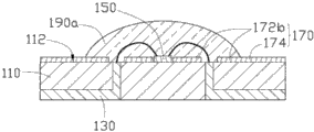
参见图1,本发明第一实施例提供的固态发光器件100,其包括:一个硅封装基板110、多个电极130、一个固态发光元件150、一个反射层170以及一个具聚光功能的透明封装体190a。Referring to FIG. 1 , a solid-state light-
硅封装基板110具有一个承载面112,承载面112可为一平面。由于硅材料具有较好的热传导性及较佳的可靠度,因此较适合用作固态发光器件100中的封装基板。The
多个电极130贯穿硅封装基板110的承载面112,其材料可选用金属,例如银、铜、铝等。具体的,所述多个电极130可贯穿整个硅封装基板110,从而其两端部分别暴露在硅封装基板110的两侧。所述多个电极130可分别具有一L型横截面。A plurality of
固态发光元件150设置在承载面112上且与多个电极130形成电连接。其中,固态发光元件150可一个或多个发光二极管芯片的组合,其可经由打线(wiring bonding)方式与多个电极130形成电连接。进一步的,发光二极管芯片可选用红光、绿、蓝、或紫外光发光二极管芯片。The solid state
反射层170设置在硅封装基板110的承载面112上,用以反射固态发光元件150受激产生的光以减少因硅封装基板110吸光而导致的光损耗,进而提升固态发光器件100的出光效率。具体的,反射层170包括一个第一反射部172a及一个第二反射部174;第一反射部172a与第二反射部174共面(coplanar)设置在承载面112上,且第一反射部172a设置在固态发光元件150与硅封装基板110的承载面112之间。其中,固态发光元件150可经由银胶等导热性能较好的粘性材料粘著在第一反射部172a上。第一反射部172a与第二反射部174的材料可为金属或白色物质。其中,金属可为银、铝、铜等,白色物质可为陶瓷粉、二氧化钛(TiO2)等。另外,可以理解的是,反射层170并不限于如图1所示之与所述多个电极130均不导通,其也可仅与所述多个电极130的其中之一不导通。The
此外,反射层170的第一反射部172a并不限于如图1所示之位于固态发光元件150及承载面112之间的情形;如图2所示,其还可在对应固态发光元件150的位置设置一开口(图2中未标示),从而固态发光元件150可经由银胶等导热性能较好的粘性材料直接粘著在承载面112上;而第一反射部172b则环绕所述固态发光元件150。在此情形下,第一反射部172b的厚度可设置为小于固态发光元件150沿承载面112的一法向量方向之高度。In addition, the first
所述具聚光功能的透明封装体190a设置在硅封装基板110的承载面112上且覆盖住固态发光元件150及反射层170的第一反射部172a。反射层170的第二反射部174则暴露在透明封装体190a的外部。所述透明封装体190a的材料折射率可设置为大于1.4,其材料可为硅胶、环氧树脂、聚碳酸酯(Polycarbonate,PC)、压克力(Polymethyl methacrylate,PMMA)等透明物质。所述透明封装体190a因具有聚光功能而可改变固态发光器件100的出光角度,以防止出射光线过度分散而导致的亮度降低。如图1所示,透明封装体190a为半球形透镜,其外表面为一沿远离固态发光元件150的方向向外凸设的弧面。可以理解的是,透明封装体190a并不限于半球形透镜,其还可为其他合适形状的透镜,只要其可改变固态发光器件100的出光角度以达到预定要求均可。例如,如图3所示,透明封装体190b为一锥形透镜,其远离固态发光元件150的一表面为非球面。The
参见图4,本发明第二实施例提供的固态发光器件200与第一实施例提供的固态发光器件100基本相同,其包括:多个电极130、一个固态发光元件150、一个反射层170以及一个具聚光功能的透明封装体190a。不同之处在于:其硅封装基板210的承载面212上向内开设有一埋入孔214;埋入孔214暴露在透明封装体190a的外部,其内收容有一个辅助元件,例如保护元件220。所述保护元件220与固态发光元件150并联,其可为稽纳二极管(Zener Diode)、肖特基二极管(Schottky Barrier Diode)、硅基二极管、晶体管或静电保护集成电路。由于保护元件220收容在埋入孔214内且位于透明封装体150的外部,其将不会遮挡固态发光元件150受激产生的光,有利于整个固态发光元件200的出光效率之提升。Referring to Fig. 4, the solid-state
另外,可以理解的是,所述保护元件220也可根据实际应用中的需要变更为其他辅助元件,例如图5所示的光感测器320。为使光感测器320能更精准地量测固态发光器件200的光强度或亮度等光学特性,所述埋入孔214则设置在透明封装体190a的覆盖区域内,从而可克服因空气与透明封装体190a之间的折射率不匹配而导致的量测精度不佳之问题。In addition, it can be understood that the
此外,本发明第一及第二实施例中的反射层170可替换一荧光粉层,所述荧光粉层包括一个第一部分及一个第二部分,第一部分与第二部分共面设置在硅封装基板110或220的承载面112或212上。所述第一部分由透明封装体190a或190b覆盖住且位于固态发光元件150与承载面112或212之间,所述第二部分暴露在透明封装体190a或190b的外部。所述荧光粉层可经由印刷、喷墨或镀膜等方式形成。所述荧光粉层作为一种波长转换层,其可吸收固态发光元件150受激产生且入射至硅封装基板110或210的承载面112或212的光线,并产生另一种波长的光线且该另一种波长的光线之传播方向是任意的。因此,荧光粉层的设置也可提升固态发光器件100或200的出光效率。In addition, the
另外,本领域技术人员还可于本发明精神内做其它变化,如变更固态发光元件的种类、透明封装体的形状、辅助元件的种类等以用于本发明等设计,只要其不偏离本发明的技术效果均可。这些依据本发明精神所做的变化,都应包含在本发明所要求保护的范围之内。In addition, those skilled in the art can also make other changes within the spirit of the present invention, such as changing the type of solid-state light-emitting element, the shape of the transparent package, the type of auxiliary components, etc. for the design of the present invention, as long as it does not deviate from the present invention The technical effect can be. These changes made according to the spirit of the present invention should be included in the scope of protection of the present invention.
Claims (10)
Priority Applications (3)
| Application Number | Priority Date | Filing Date | Title |
|---|---|---|---|
| CN2007102029837A CN101459211B (en) | 2007-12-11 | 2007-12-11 | Solid illuminating device |
| US12/202,555 US7994518B2 (en) | 2007-12-11 | 2008-09-02 | Light-emitting diode |
| EP08253440A EP2071637A2 (en) | 2007-12-11 | 2008-10-22 | Light emitting diode |
Applications Claiming Priority (1)
| Application Number | Priority Date | Filing Date | Title |
|---|---|---|---|
| CN2007102029837A CN101459211B (en) | 2007-12-11 | 2007-12-11 | Solid illuminating device |
Publications (2)
| Publication Number | Publication Date |
|---|---|
| CN101459211A CN101459211A (en) | 2009-06-17 |
| CN101459211B true CN101459211B (en) | 2011-03-02 |
Family
ID=40329088
Family Applications (1)
| Application Number | Title | Priority Date | Filing Date |
|---|---|---|---|
| CN2007102029837A Expired - Fee Related CN101459211B (en) | 2007-12-11 | 2007-12-11 | Solid illuminating device |
Country Status (3)
| Country | Link |
|---|---|
| US (1) | US7994518B2 (en) |
| EP (1) | EP2071637A2 (en) |
| CN (1) | CN101459211B (en) |
Cited By (1)
| Publication number | Priority date | Publication date | Assignee | Title |
|---|---|---|---|---|
| CN103000785A (en) * | 2012-11-05 | 2013-03-27 | 何忠亮 | LED luminous structure and method for manufacturing same |
Families Citing this family (40)
| Publication number | Priority date | Publication date | Assignee | Title |
|---|---|---|---|---|
| TWI426206B (en) * | 2008-12-25 | 2014-02-11 | 友達光電股份有限公司 | Light-emitting diode device |
| KR101064026B1 (en) * | 2009-02-17 | 2011-09-08 | 엘지이노텍 주식회사 | Light emitting device package and manufacturing method thereof |
| JP5343831B2 (en) * | 2009-04-16 | 2013-11-13 | 日亜化学工業株式会社 | Light emitting device |
| US8474997B2 (en) * | 2010-04-07 | 2013-07-02 | Appotronics Corporation Limited | High brightness illumination device using double-sided excitation of wavelength conversion materials |
| TWI472067B (en) * | 2010-04-28 | 2015-02-01 | Lg伊諾特股份有限公司 | Optical package and method of manufacturing same |
| KR101130137B1 (en) * | 2010-07-02 | 2012-03-28 | 연세대학교 산학협력단 | Light emitting diode module |
| TWI478319B (en) * | 2010-07-20 | 2015-03-21 | 晶元光電股份有限公司 | Integrated illuminating device and manufacturing method thereof |
| USD707192S1 (en) | 2010-11-18 | 2014-06-17 | Cree, Inc. | Light emitting device |
| US8564000B2 (en) | 2010-11-22 | 2013-10-22 | Cree, Inc. | Light emitting devices for light emitting diodes (LEDs) |
| USD721339S1 (en) | 2010-12-03 | 2015-01-20 | Cree, Inc. | Light emitter device |
| USD712850S1 (en) | 2010-11-18 | 2014-09-09 | Cree, Inc. | Light emitter device |
| CN102468406B (en) * | 2010-11-19 | 2014-11-05 | 展晶科技(深圳)有限公司 | Light emitting diode packaging structure and manufacturing method thereof |
| US9300062B2 (en) | 2010-11-22 | 2016-03-29 | Cree, Inc. | Attachment devices and methods for light emitting devices |
| US8575639B2 (en) | 2011-02-16 | 2013-11-05 | Cree, Inc. | Light emitting devices for light emitting diodes (LEDs) |
| US9490235B2 (en) | 2010-11-22 | 2016-11-08 | Cree, Inc. | Light emitting devices, systems, and methods |
| US9000470B2 (en) | 2010-11-22 | 2015-04-07 | Cree, Inc. | Light emitter devices |
| US8624271B2 (en) | 2010-11-22 | 2014-01-07 | Cree, Inc. | Light emitting devices |
| CN102479909B (en) * | 2010-11-24 | 2014-12-10 | 展晶科技(深圳)有限公司 | Light emitting diode |
| USD706231S1 (en) | 2010-12-03 | 2014-06-03 | Cree, Inc. | Light emitting device |
| US8809880B2 (en) | 2011-02-16 | 2014-08-19 | Cree, Inc. | Light emitting diode (LED) chips and devices for providing failure mitigation in LED arrays |
| US8455908B2 (en) | 2011-02-16 | 2013-06-04 | Cree, Inc. | Light emitting devices |
| USD702653S1 (en) | 2011-10-26 | 2014-04-15 | Cree, Inc. | Light emitting device component |
| TWI517452B (en) * | 2011-03-02 | 2016-01-11 | 建準電機工業股份有限公司 | Polycrystalline package structure of luminescent crystal |
| USD705181S1 (en) | 2011-10-26 | 2014-05-20 | Cree, Inc. | Light emitting device component |
| CN104081112B (en) | 2011-11-07 | 2016-03-16 | 克利公司 | High voltage array light emitting diode (LED) device, apparatus and method |
| US9735198B2 (en) | 2012-03-30 | 2017-08-15 | Cree, Inc. | Substrate based light emitter devices, components, and related methods |
| US10134961B2 (en) | 2012-03-30 | 2018-11-20 | Cree, Inc. | Submount based surface mount device (SMD) light emitter components and methods |
| US9345091B2 (en) | 2013-02-08 | 2016-05-17 | Cree, Inc. | Light emitting device (LED) light fixture control systems and related methods |
| US10295124B2 (en) * | 2013-02-27 | 2019-05-21 | Cree, Inc. | Light emitter packages and methods |
| DE102013215326A1 (en) * | 2013-04-30 | 2014-10-30 | Tridonic Jennersdorf Gmbh | LED module with highly reflective surface |
| USD739565S1 (en) | 2013-06-27 | 2015-09-22 | Cree, Inc. | Light emitter unit |
| USD740453S1 (en) | 2013-06-27 | 2015-10-06 | Cree, Inc. | Light emitter unit |
| CN104282830B (en) * | 2013-07-12 | 2018-01-30 | 展晶科技(深圳)有限公司 | LED Module |
| JP6201617B2 (en) * | 2013-10-17 | 2017-09-27 | 日亜化学工業株式会社 | Light emitting device |
| CN104393159A (en) * | 2014-10-21 | 2015-03-04 | 深圳市瑞丰光电子股份有限公司 | LED lamp filament |
| EP3239592B1 (en) * | 2014-11-18 | 2021-03-31 | Seoul Semiconductor Co., Ltd. | Light emitting device and vehicular lamp comprising same |
| US9252337B1 (en) | 2014-12-22 | 2016-02-02 | Bridgelux, Inc. | Composite substrate for light emitting diodes |
| USD823492S1 (en) | 2016-10-04 | 2018-07-17 | Cree, Inc. | Light emitting device |
| CN118712309A (en) * | 2020-11-20 | 2024-09-27 | 隆达电子股份有限公司 | Light-emitting device, backlight plate and display panel |
| JP2024118546A (en) * | 2023-02-21 | 2024-09-02 | シャープディスプレイテクノロジー株式会社 | Illumination device, display device, and method for manufacturing an illumination device |
Citations (3)
| Publication number | Priority date | Publication date | Assignee | Title |
|---|---|---|---|---|
| CN1355571A (en) * | 2000-11-23 | 2002-06-26 | 诠兴开发科技股份有限公司 | Packaging method of light emitting diode |
| CN1679179A (en) * | 2002-09-02 | 2005-10-05 | 帝希欧有限公社 | Surface Mount Light Emitting Diodes |
| CN1860620A (en) * | 2003-09-30 | 2006-11-08 | 株式会社东芝 | Light emitting device |
Family Cites Families (8)
| Publication number | Priority date | Publication date | Assignee | Title |
|---|---|---|---|---|
| JP2735089B2 (en) | 1993-03-22 | 1998-04-02 | 株式会社サトミ製作所 | How to remove light and fine foreign matter |
| TWM246811U (en) | 2003-07-28 | 2004-10-11 | Lightop Technology Co Ltd | Improved light emitting diode structure with fluorescent ink |
| US7329905B2 (en) * | 2004-06-30 | 2008-02-12 | Cree, Inc. | Chip-scale methods for packaging light emitting devices and chip-scale packaged light emitting devices |
| TWI249257B (en) | 2004-09-24 | 2006-02-11 | Epistar Corp | Illumination apparatus |
| JP4176703B2 (en) * | 2004-11-25 | 2008-11-05 | 松下電器産業株式会社 | Semiconductor light emitting device, lighting device, portable communication device, camera, and manufacturing method |
| TW200721525A (en) | 2005-11-16 | 2007-06-01 | High Power Lighting Corp | Package structure of combining zener diode chip and light-emitting diode chip |
| US7607815B2 (en) * | 2006-11-27 | 2009-10-27 | Avago Technologies Ecbu Ip (Singapore) Pte. Ltd. | Low profile and high efficiency lighting device for backlighting applications |
| US20080246397A1 (en) * | 2007-04-04 | 2008-10-09 | Bily Wang | Manufacturing method of white light led and structure thereof |
-
2007
- 2007-12-11 CN CN2007102029837A patent/CN101459211B/en not_active Expired - Fee Related
-
2008
- 2008-09-02 US US12/202,555 patent/US7994518B2/en not_active Expired - Fee Related
- 2008-10-22 EP EP08253440A patent/EP2071637A2/en not_active Withdrawn
Patent Citations (3)
| Publication number | Priority date | Publication date | Assignee | Title |
|---|---|---|---|---|
| CN1355571A (en) * | 2000-11-23 | 2002-06-26 | 诠兴开发科技股份有限公司 | Packaging method of light emitting diode |
| CN1679179A (en) * | 2002-09-02 | 2005-10-05 | 帝希欧有限公社 | Surface Mount Light Emitting Diodes |
| CN1860620A (en) * | 2003-09-30 | 2006-11-08 | 株式会社东芝 | Light emitting device |
Cited By (1)
| Publication number | Priority date | Publication date | Assignee | Title |
|---|---|---|---|---|
| CN103000785A (en) * | 2012-11-05 | 2013-03-27 | 何忠亮 | LED luminous structure and method for manufacturing same |
Also Published As
| Publication number | Publication date |
|---|---|
| US7994518B2 (en) | 2011-08-09 |
| EP2071637A2 (en) | 2009-06-17 |
| US20090146155A1 (en) | 2009-06-11 |
| CN101459211A (en) | 2009-06-17 |
Similar Documents
| Publication | Publication Date | Title |
|---|---|---|
| CN101459211B (en) | Solid illuminating device | |
| US8063411B2 (en) | Photoelectric semiconductor device capable of generating uniform compound lights | |
| CN102130109B (en) | Light emitting device and light unit using the same | |
| CN101567366A (en) | Light emitting diode | |
| CN103682068A (en) | Light emitting device | |
| CN206921858U (en) | Light-emitting device | |
| CN101442086A (en) | Light emitting diode combination | |
| KR20140095913A (en) | Light emitting module and light apparatus having thereof | |
| KR20140049274A (en) | Light source module and lighting system having the same | |
| CN102054828A (en) | Packaging shell and packaging structure of edge type light emitting component | |
| KR20170052208A (en) | Optical plate, lighting device, and lighting module | |
| KR102432222B1 (en) | Optical plate, lighting device, and lighting module | |
| CN103531583A (en) | LED Array Module | |
| KR101946921B1 (en) | Light emitting apparatus and lighting system having the same | |
| KR102075080B1 (en) | Light emitting device, manufactured method of the light emitting deviceand lighting apparatus | |
| KR102451866B1 (en) | Optical plate, lighting device, and lighting module | |
| KR20170052204A (en) | Optical plate, lighting device, and lighting module | |
| TW200929596A (en) | Solid state light emitting device | |
| KR102531846B1 (en) | Optical plate, lighting device, and lighting module | |
| KR101936289B1 (en) | Light emitting device | |
| CN101452922B (en) | Light emitting unit | |
| CN201527994U (en) | Side light type light emitting element packaging shell and packaging structure | |
| KR102531104B1 (en) | Optical plate, lighting device, and lighting module | |
| KR102450123B1 (en) | Optical plate, lighting device, and lighting module | |
| CN104716130A (en) | Light emitting diode capable of achieving light mixing |
Legal Events
| Date | Code | Title | Description |
|---|---|---|---|
| C06 | Publication | ||
| PB01 | Publication | ||
| C10 | Entry into substantive examination | ||
| SE01 | Entry into force of request for substantive examination | ||
| C14 | Grant of patent or utility model | ||
| GR01 | Patent grant | ||
| C56 | Change in the name or address of the patentee | ||
| CP01 | Change in the name or title of a patent holder |
Address after: 201600 Shanghai City, Songjiang District Songjiang Industrial Zone West science and Technology Industrial Park No. 500 Wen Ji Lu Patentee after: Foxsemicon Semiconductor Precision (Shanghai) Inc. Patentee after: Foxsemicon Integrated Technology Inc. Address before: 201600 Shanghai City, Songjiang District Songjiang Industrial Zone West science and Technology Industrial Park No. 500 Wen Ji Lu Patentee before: Foxsemicon Semiconductor Precision (Shanghai) Inc. Patentee before: Foxsemicon Integrated Technology Inc. |
|
| C17 | Cessation of patent right | ||
| CF01 | Termination of patent right due to non-payment of annual fee |
Granted publication date: 20110302 Termination date: 20131211 |