CN101256309A - LED backlight unit and LCD unit - Google Patents
LED backlight unit and LCD unit Download PDFInfo
- Publication number
- CN101256309A CN101256309A CNA2008100823304A CN200810082330A CN101256309A CN 101256309 A CN101256309 A CN 101256309A CN A2008100823304 A CNA2008100823304 A CN A2008100823304A CN 200810082330 A CN200810082330 A CN 200810082330A CN 101256309 A CN101256309 A CN 101256309A
- Authority
- CN
- China
- Prior art keywords
- led
- anode
- substrate
- cathode
- wiring
- Prior art date
- Legal status (The legal status is an assumption and is not a legal conclusion. Google has not performed a legal analysis and makes no representation as to the accuracy of the status listed.)
- Granted
Links
- 239000000758 substrate Substances 0.000 claims abstract description 85
- 229910010272 inorganic material Inorganic materials 0.000 claims abstract description 13
- 239000011147 inorganic material Substances 0.000 claims abstract description 13
- 239000000463 material Substances 0.000 claims description 31
- 238000005530 etching Methods 0.000 claims description 18
- 230000005540 biological transmission Effects 0.000 claims description 4
- 239000011248 coating agent Substances 0.000 claims 2
- 238000000576 coating method Methods 0.000 claims 2
- 239000002131 composite material Substances 0.000 claims 1
- 239000012528 membrane Substances 0.000 claims 1
- 239000000203 mixture Substances 0.000 claims 1
- 239000010408 film Substances 0.000 abstract description 43
- 239000010409 thin film Substances 0.000 abstract description 39
- OAICVXFJPJFONN-UHFFFAOYSA-N Phosphorus Chemical compound [P] OAICVXFJPJFONN-UHFFFAOYSA-N 0.000 abstract description 30
- 238000000034 method Methods 0.000 description 32
- 230000008569 process Effects 0.000 description 16
- MHAJPDPJQMAIIY-UHFFFAOYSA-N Hydrogen peroxide Chemical compound OO MHAJPDPJQMAIIY-UHFFFAOYSA-N 0.000 description 10
- NBIIXXVUZAFLBC-UHFFFAOYSA-N Phosphoric acid Chemical compound OP(O)(O)=O NBIIXXVUZAFLBC-UHFFFAOYSA-N 0.000 description 10
- 239000010410 layer Substances 0.000 description 9
- 229910052751 metal Inorganic materials 0.000 description 9
- 239000002184 metal Substances 0.000 description 9
- 239000002344 surface layer Substances 0.000 description 9
- PXHVJJICTQNCMI-UHFFFAOYSA-N Nickel Chemical compound [Ni] PXHVJJICTQNCMI-UHFFFAOYSA-N 0.000 description 8
- 229910052782 aluminium Inorganic materials 0.000 description 8
- XAGFODPZIPBFFR-UHFFFAOYSA-N aluminium Chemical compound [Al] XAGFODPZIPBFFR-UHFFFAOYSA-N 0.000 description 8
- PCHJSUWPFVWCPO-UHFFFAOYSA-N gold Chemical compound [Au] PCHJSUWPFVWCPO-UHFFFAOYSA-N 0.000 description 8
- 229910052737 gold Inorganic materials 0.000 description 8
- 239000010931 gold Substances 0.000 description 8
- 229910002601 GaN Inorganic materials 0.000 description 7
- 238000010586 diagram Methods 0.000 description 7
- 230000001681 protective effect Effects 0.000 description 7
- 239000004065 semiconductor Substances 0.000 description 6
- JMASRVWKEDWRBT-UHFFFAOYSA-N Gallium nitride Chemical compound [Ga]#N JMASRVWKEDWRBT-UHFFFAOYSA-N 0.000 description 5
- 229910000147 aluminium phosphate Inorganic materials 0.000 description 5
- 239000001257 hydrogen Substances 0.000 description 5
- 229910052739 hydrogen Inorganic materials 0.000 description 5
- XLYOFNOQVPJJNP-UHFFFAOYSA-N water Substances O XLYOFNOQVPJJNP-UHFFFAOYSA-N 0.000 description 5
- KRHYYFGTRYWZRS-UHFFFAOYSA-N Fluorane Chemical compound F KRHYYFGTRYWZRS-UHFFFAOYSA-N 0.000 description 4
- VEXZGXHMUGYJMC-UHFFFAOYSA-N Hydrochloric acid Chemical compound Cl VEXZGXHMUGYJMC-UHFFFAOYSA-N 0.000 description 4
- RTAQQCXQSZGOHL-UHFFFAOYSA-N Titanium Chemical compound [Ti] RTAQQCXQSZGOHL-UHFFFAOYSA-N 0.000 description 4
- 229910052759 nickel Inorganic materials 0.000 description 4
- 229920001721 polyimide Polymers 0.000 description 4
- VYPSYNLAJGMNEJ-UHFFFAOYSA-N silicon dioxide Inorganic materials O=[Si]=O VYPSYNLAJGMNEJ-UHFFFAOYSA-N 0.000 description 4
- 229910052719 titanium Inorganic materials 0.000 description 4
- 239000010936 titanium Substances 0.000 description 4
- 238000000151 deposition Methods 0.000 description 3
- 230000008021 deposition Effects 0.000 description 3
- 238000000206 photolithography Methods 0.000 description 3
- 229910052814 silicon oxide Inorganic materials 0.000 description 3
- JBRZTFJDHDCESZ-UHFFFAOYSA-N AsGa Chemical compound [As]#[Ga] JBRZTFJDHDCESZ-UHFFFAOYSA-N 0.000 description 2
- 229910001218 Gallium arsenide Inorganic materials 0.000 description 2
- MDPILPRLPQYEEN-UHFFFAOYSA-N aluminium arsenide Chemical compound [As]#[Al] MDPILPRLPQYEEN-UHFFFAOYSA-N 0.000 description 2
- RNQKDQAVIXDKAG-UHFFFAOYSA-N aluminum gallium Chemical compound [Al].[Ga] RNQKDQAVIXDKAG-UHFFFAOYSA-N 0.000 description 2
- PMHQVHHXPFUNSP-UHFFFAOYSA-M copper(1+);methylsulfanylmethane;bromide Chemical compound Br[Cu].CSC PMHQVHHXPFUNSP-UHFFFAOYSA-M 0.000 description 2
- 239000004973 liquid crystal related substance Substances 0.000 description 2
- 238000004519 manufacturing process Methods 0.000 description 2
- 239000011159 matrix material Substances 0.000 description 2
- 238000002488 metal-organic chemical vapour deposition Methods 0.000 description 2
- 229910052594 sapphire Inorganic materials 0.000 description 2
- 239000010980 sapphire Substances 0.000 description 2
- 238000002834 transmittance Methods 0.000 description 2
- 238000001947 vapour-phase growth Methods 0.000 description 2
- 229910052684 Cerium Inorganic materials 0.000 description 1
- 229910052688 Gadolinium Inorganic materials 0.000 description 1
- GYHNNYVSQQEPJS-UHFFFAOYSA-N Gallium Chemical compound [Ga] GYHNNYVSQQEPJS-UHFFFAOYSA-N 0.000 description 1
- 239000004642 Polyimide Substances 0.000 description 1
- 229910052771 Terbium Inorganic materials 0.000 description 1
- 230000002238 attenuated effect Effects 0.000 description 1
- NWAIGJYBQQYSPW-UHFFFAOYSA-N azanylidyneindigane Chemical compound [In]#N NWAIGJYBQQYSPW-UHFFFAOYSA-N 0.000 description 1
- 229910052788 barium Inorganic materials 0.000 description 1
- 229910052791 calcium Inorganic materials 0.000 description 1
- 230000008859 change Effects 0.000 description 1
- 230000006866 deterioration Effects 0.000 description 1
- 239000010432 diamond Substances 0.000 description 1
- 229910003460 diamond Inorganic materials 0.000 description 1
- 238000009792 diffusion process Methods 0.000 description 1
- 230000009977 dual effect Effects 0.000 description 1
- 238000005401 electroluminescence Methods 0.000 description 1
- 229910052733 gallium Inorganic materials 0.000 description 1
- 239000011521 glass Substances 0.000 description 1
- 229910052738 indium Inorganic materials 0.000 description 1
- APFVFJFRJDLVQX-UHFFFAOYSA-N indium atom Chemical compound [In] APFVFJFRJDLVQX-UHFFFAOYSA-N 0.000 description 1
- 239000011261 inert gas Substances 0.000 description 1
- 229910052749 magnesium Inorganic materials 0.000 description 1
- 230000004048 modification Effects 0.000 description 1
- 238000012986 modification Methods 0.000 description 1
- 230000003647 oxidation Effects 0.000 description 1
- 238000007254 oxidation reaction Methods 0.000 description 1
- 238000000059 patterning Methods 0.000 description 1
- 239000010453 quartz Substances 0.000 description 1
- 230000009467 reduction Effects 0.000 description 1
- LIVNPJMFVYWSIS-UHFFFAOYSA-N silicon monoxide Chemical compound [Si-]#[O+] LIVNPJMFVYWSIS-UHFFFAOYSA-N 0.000 description 1
- 229910052712 strontium Inorganic materials 0.000 description 1
- 229910052725 zinc Inorganic materials 0.000 description 1
Images


Classifications
-
- G—PHYSICS
- G02—OPTICS
- G02F—OPTICAL DEVICES OR ARRANGEMENTS FOR THE CONTROL OF LIGHT BY MODIFICATION OF THE OPTICAL PROPERTIES OF THE MEDIA OF THE ELEMENTS INVOLVED THEREIN; NON-LINEAR OPTICS; FREQUENCY-CHANGING OF LIGHT; OPTICAL LOGIC ELEMENTS; OPTICAL ANALOGUE/DIGITAL CONVERTERS
- G02F1/00—Devices or arrangements for the control of the intensity, colour, phase, polarisation or direction of light arriving from an independent light source, e.g. switching, gating or modulating; Non-linear optics
- G02F1/01—Devices or arrangements for the control of the intensity, colour, phase, polarisation or direction of light arriving from an independent light source, e.g. switching, gating or modulating; Non-linear optics for the control of the intensity, phase, polarisation or colour
- G02F1/13—Devices or arrangements for the control of the intensity, colour, phase, polarisation or direction of light arriving from an independent light source, e.g. switching, gating or modulating; Non-linear optics for the control of the intensity, phase, polarisation or colour based on liquid crystals, e.g. single liquid crystal display cells
- G02F1/133—Constructional arrangements; Operation of liquid crystal cells; Circuit arrangements
- G02F1/1333—Constructional arrangements; Manufacturing methods
- G02F1/1335—Structural association of cells with optical devices, e.g. polarisers or reflectors
- G02F1/1336—Illuminating devices
- G02F1/133617—Illumination with ultraviolet light; Luminescent elements or materials associated to the cell
-
- G—PHYSICS
- G02—OPTICS
- G02F—OPTICAL DEVICES OR ARRANGEMENTS FOR THE CONTROL OF LIGHT BY MODIFICATION OF THE OPTICAL PROPERTIES OF THE MEDIA OF THE ELEMENTS INVOLVED THEREIN; NON-LINEAR OPTICS; FREQUENCY-CHANGING OF LIGHT; OPTICAL LOGIC ELEMENTS; OPTICAL ANALOGUE/DIGITAL CONVERTERS
- G02F1/00—Devices or arrangements for the control of the intensity, colour, phase, polarisation or direction of light arriving from an independent light source, e.g. switching, gating or modulating; Non-linear optics
- G02F1/01—Devices or arrangements for the control of the intensity, colour, phase, polarisation or direction of light arriving from an independent light source, e.g. switching, gating or modulating; Non-linear optics for the control of the intensity, phase, polarisation or colour
- G02F1/13—Devices or arrangements for the control of the intensity, colour, phase, polarisation or direction of light arriving from an independent light source, e.g. switching, gating or modulating; Non-linear optics for the control of the intensity, phase, polarisation or colour based on liquid crystals, e.g. single liquid crystal display cells
- G02F1/133—Constructional arrangements; Operation of liquid crystal cells; Circuit arrangements
- G02F1/1333—Constructional arrangements; Manufacturing methods
- G02F1/1335—Structural association of cells with optical devices, e.g. polarisers or reflectors
- G02F1/1336—Illuminating devices
- G02F1/133602—Direct backlight
- G02F1/133603—Direct backlight with LEDs
-
- H—ELECTRICITY
- H05—ELECTRIC TECHNIQUES NOT OTHERWISE PROVIDED FOR
- H05B—ELECTRIC HEATING; ELECTRIC LIGHT SOURCES NOT OTHERWISE PROVIDED FOR; CIRCUIT ARRANGEMENTS FOR ELECTRIC LIGHT SOURCES, IN GENERAL
- H05B45/00—Circuit arrangements for operating light-emitting diodes [LED]
- H05B45/30—Driver circuits
- H05B45/345—Current stabilisation; Maintaining constant current
Landscapes
- Physics & Mathematics (AREA)
- Nonlinear Science (AREA)
- Mathematical Physics (AREA)
- Chemical & Material Sciences (AREA)
- Crystallography & Structural Chemistry (AREA)
- General Physics & Mathematics (AREA)
- Optics & Photonics (AREA)
- Led Device Packages (AREA)
- Led Devices (AREA)
- Liquid Crystal (AREA)
- Planar Illumination Modules (AREA)
Abstract
LED背光装置和LCD装置。一种LED背光装置,包括具有透光性的基板以及固定于该基板的第一表面的LED薄膜分层结构。该LED薄膜分层结构是由外延生长的无机材料层形成为P-N结装置。阳极电极和阴极电极形成于该LED薄膜分层结构上。阳极驱动器IC和阴极驱动器IC用于驱动该LED薄膜分层结构。布线结构电连接该阳极驱动器IC和该LED薄膜分层结构的该阳极电极,并电连接该阴极驱动器IC和该LED薄膜分层结构的该阴极电极。荧光体形成于该基板的与第一表面相对的第二表面上。
LED backlight unit and LCD unit. An LED backlight device comprises a light-transmitting substrate and an LED film layered structure fixed on the first surface of the substrate. The layered structure of the LED thin film is formed as a PN junction device by an epitaxially grown inorganic material layer. An anode electrode and a cathode electrode are formed on the LED film layered structure. An anode driver IC and a cathode driver IC are used to drive the LED thin film layered structure. The wiring structure electrically connects the anode driver IC and the anode electrode of the LED thin film layered structure, and electrically connects the cathode driver IC and the cathode electrode of the LED thin film layered structure. Phosphor is formed on the second surface of the substrate opposite to the first surface.
Description
技术领域 technical field
本发明涉及LED背光装置和使用该LED背光装置的LCD装置。The present invention relates to an LED backlight device and an LCD device using the LED backlight device.
背景技术 Background technique
在一般LCD(液晶显示器)装置中,光是由光源发射并入射在LCD面板上。LCD装置配置成改变布置于LCD面板上的液晶(像素)的分子配向(molecular alignment),从而利用透过LCD面板的光来显示图像。In a general LCD (Liquid Crystal Display) device, light is emitted from a light source and incident on an LCD panel. The LCD device is configured to change molecular alignment of liquid crystals (pixels) arranged on the LCD panel, thereby displaying images using light transmitted through the LCD panel.
这种LCD装置中使用的光源被称为背光,因为光源置于LCD面板的背侧(即,与LCD面板的显示表面相对的一侧)。常规光源是由冷阴极射线管或半导体发光元件组成。使用半导体发光元件的光源已经广泛使用,这是因为这种光源具有长寿命且有助于减小功耗。The light source used in such an LCD device is called a backlight because the light source is placed on the backside of the LCD panel (ie, the side opposite the display surface of the LCD panel). Conventional light sources are composed of cold cathode ray tubes or semiconductor light emitting elements. A light source using a semiconductor light emitting element has been widely used because it has a long life and contributes to a reduction in power consumption.
就此而言,已知一种使用LED(发光二极管)作为上述半导体发光元件的表面发射光源。这种表面发射光源具有称为导光板或光漫射板的板状构件用于引导由LED发射的光。由LED发射的光入射到导光板的端面上。导光板反射和漫射沿与导光板表面垂直的方向的入射光,并从导光板表面发射该光(见专利文献1)。In this regard, there is known a surface-emitting light source using an LED (Light Emitting Diode) as the above-mentioned semiconductor light emitting element. Such a surface-emitting light source has a plate-shaped member called a light guide plate or a light-diffusing plate for guiding light emitted by LEDs. The light emitted by the LED is incident on the end surface of the light guide plate. The light guide plate reflects and diffuses incident light in a direction perpendicular to the surface of the light guide plate, and emits the light from the surface of the light guide plate (see Patent Document 1).
专利文献1:日本特开平专利公开No.11-232920。Patent Document 1: Japanese Laid-Open Patent Publication No. 11-232920.
然而,在常规背光装置中,随着与入射表面(即,导光板的端面)的距离增大,在导光板内部漫射的光由于反射和漫射而趋于衰减。因此,为了在整个表面上均匀地获得高的光强度,导光板的结构变得复杂且LED背光装置需要厚。However, in the conventional backlight device, light diffused inside the light guide plate tends to be attenuated due to reflection and diffusion as the distance from the incident surface (ie, the end surface of the light guide plate) increases. Therefore, in order to uniformly obtain high light intensity over the entire surface, the structure of the light guide plate becomes complicated and the LED backlight needs to be thick.
发明内容 Contents of the invention
本发明旨在解决上述问题,且本发明的目的是提供一种能够提供高的光强度的薄LED背光装置,以及使用该LED背光装置的LCD装置。The present invention aims to solve the above-mentioned problems, and an object of the present invention is to provide a thin LED backlight device capable of providing high light intensity, and an LCD device using the LED backlight device.
本发明提供了一种背光装置,包括:基板,其具有透光性并具有第一表面和与该第一表面相对的第二表面;LED薄膜分层结构,形成于该基板的第一表面上,该LED薄膜分层结构是由外延生长的无机材料层形成为P-N结装置;阳极电极和阴极电极,形成于该LED薄膜分层结构上;阳极驱动器IC和阴极驱动器IC,用于驱动该LED薄膜分层结构;布线结构,电连接该阳极驱动器IC和该LED薄膜分层结构的阳极电极,并电连接该阴极驱动器IC和该LED薄膜分层结构的阴极电极;以及荧光体,形成于该基板的第二表面上。The invention provides a backlight device, comprising: a substrate having light transmission and having a first surface and a second surface opposite to the first surface; an LED film layered structure formed on the first surface of the substrate , the LED thin film layered structure is formed by epitaxially grown inorganic material layers as a P-N junction device; the anode electrode and the cathode electrode are formed on the LED thin film layered structure; the anode driver IC and the cathode driver IC are used to drive the LED film layered structure; wiring structure, electrically connecting the anode driver IC and the anode electrode of the LED film layered structure, and electrically connecting the cathode driver IC and the cathode electrode of the LED film layered structure; and phosphor, formed on the on the second surface of the substrate.
由于该LED背光装置具有形成于基板(具有透光性)的第二表面上的荧光体,该第二表面与其上形成该LED薄膜分层结构的第一表面相对,因此可以获得提供高的光强度的薄LED背光装置。Since the LED backlight device has phosphors formed on the second surface of the substrate (having light transmittance), which is opposite to the first surface on which the LED thin film layered structure is formed, it is possible to provide high light Intensity thin LED backlight unit.
通过下文的详细描述,本发明的其他应用范围将显而易见。然而应理解,这些详细描述和具体示例仅示出本发明的优选实施例,仅仅是出于说明的目的,因为显而易见的是本领域技术人员通过该详细描述可以在本发明的精神和范围内进行各种变化和改进。Other scopes of applicability of the present invention will become apparent from the detailed description below. It should be understood, however, that the detailed description and specific examples illustrate the preferred embodiment of the invention, and are given for illustration purposes only, since it will be apparent to those skilled in the art from this detailed description that other works within the spirit and scope of the invention can be made. Various changes and improvements.
附图说明 Description of drawings
附图中:In the attached picture:
图1为示出本发明第一实施例的包括LED背光装置的LCD装置的主要部件的侧面剖视图;1 is a side sectional view showing main parts of an LCD device including an LED backlight device according to a first embodiment of the present invention;
图2为示出从第一表面侧观看的本发明第一实施例的LED背光装置的透视图;2 is a perspective view showing the LED backlight device of the first embodiment of the present invention viewed from the first surface side;
图3为示出从第二表面侧观看的本发明第一实施例的LED背光装置的透视图;3 is a perspective view showing the LED backlight device of the first embodiment of the present invention viewed from the second surface side;
图4为示出本发明第一实施例的用于剥离LED薄膜分层结构的工艺的示意图;4 is a schematic diagram showing the process for peeling off the layered structure of the LED film according to the first embodiment of the present invention;
图5为示出本发明第一实施例的将LED薄膜分层结构固定到基板的工艺的示意图;5 is a schematic diagram showing the process of fixing the LED film layered structure to the substrate according to the first embodiment of the present invention;
图6为示出本发明第二实施例的LED背光装置的侧面剖视图;6 is a side sectional view showing an LED backlight device according to a second embodiment of the present invention;
图7为示出从第一表面侧观看的本发明第二实施例的LED背光装置的透视图;7 is a perspective view showing an LED backlight device of a second embodiment of the present invention viewed from the first surface side;
图8为示出本发明第二实施例的用于剥离LED薄膜分层结构的工艺的示意图;8 is a schematic diagram showing a process for peeling off the layered structure of the LED film according to the second embodiment of the present invention;
图9为示出本发明第二实施例的将LED薄膜分层结构固定到基板的工艺的示意图;9 is a schematic diagram showing the process of fixing the LED thin film layered structure to the substrate according to the second embodiment of the present invention;
图10为示出本发明第二实施例的用于划分LED薄膜分层结构的工艺的示意图;10 is a schematic diagram showing the process for dividing the LED film layered structure according to the second embodiment of the present invention;
图11为示出从第一表面侧观看的本发明第三实施例的LED背光装置的透视图;以及11 is a perspective view showing an LED backlight device of a third embodiment of the present invention viewed from the first surface side; and
图12为示出本发明第四实施例的LED背光装置的侧面剖视图。12 is a side sectional view showing an LED backlight device according to a fourth embodiment of the present invention.
具体实施方式 Detailed ways
下面参考附图描述本发明实施例。Embodiments of the present invention are described below with reference to the drawings.
第一实施例first embodiment
图1为示出本发明第一实施例的包括LED背光装置的LCD装置的主要部件的侧面剖视图。图2为示出从第一表面侧观看的本发明第一实施例的LED背光装置的透视图。图3为示出从第二表面侧观看的本发明第一实施例的LED背光装置的透视图。1 is a side sectional view showing main parts of an LCD device including an LED backlight device according to a first embodiment of the present invention. 2 is a perspective view showing the LED backlight device of the first embodiment of the present invention viewed from the first surface side. 3 is a perspective view showing the LED backlight device of the first embodiment of the present invention viewed from the second surface side.
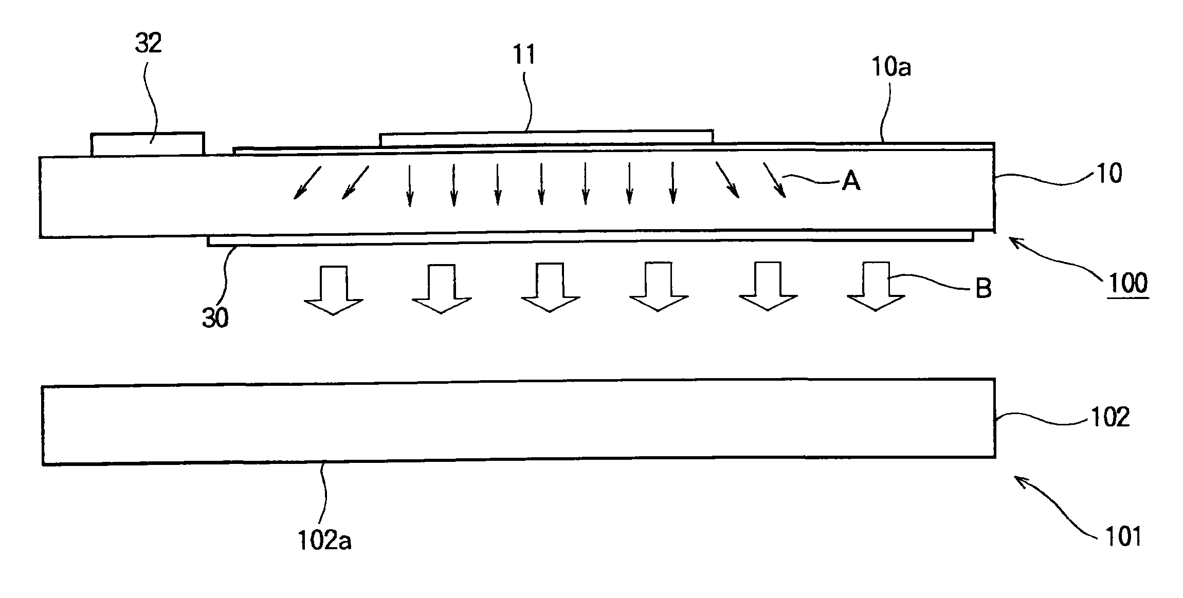
在图1,第一实施例的LED背光装置100用作LCD装置101中的光源,并置于LCD面板102的背侧(即,与LCD面板102的显示表面102a相对的一侧)。LCD面板102为透射类型。In FIG. 1 , the
LED背光装置100包括平板形状的基板10。LED背光装置100还包括:固定到基板10的第一表面(即,图1中的上表面)的LED 11(即,LED薄膜分层结构);以及固定到基板10的第二表面(即,图1中的下表面)的荧光体30。如图2所示,用于驱动LED 11的阳极驱动器IC 31和阴极驱动器IC 32置于基板10的第一表面上。阳极驱动器IC 31连接到阳极布线12的端部,(形成于基板10的第一表面上的)阳极布线12连接到LED 11的阳极电极14。阴极驱动器IC 32连接到阴极布线13的端部,(形成于基板10的第一表面上的)阴极布线13连接到LED11的阴极电极15。阳极布线12和阴极布线13构成用于将阳极驱动器IC 31电连接到LED 11以及将阴极驱动器IC 32电连接到LED 11的布线结构。The
在图1,基板10是由具有透光性的石英或玻璃组成的板形成。荧光体30在暴露于近紫外线或紫外线时发射白光。荧光体30涂覆在基板10的第二表面上。In FIG. 1 , a
荧光体30可以通过混合发射红光的荧光体、发射绿光的荧光体以及发射蓝光的荧光体来形成。更具体而言,发射红光的荧光体例如为Y2O3:Eu或(Y,Gd)BO3:Eu。发射绿光的荧光体例如为LaPO4:Ce,Tb或Zn2SiO:Mn。发射蓝光的荧光体例如为(Sr,Ca,Ba,Mg)5(PO4)3Cl或BaMgAl10O17:Eu。The
发射红光的荧光体不限于上述材料,而可以由当暴露于波长范围为300nm至450nm的近紫外线或紫外线时发射波长范围为620nm至710nm的任意材料形成。发射绿光的荧光体可以由当暴露于波长范围为300nm至450nm的近紫外线或紫外线时发射波长范围为500nm至580nm的任意材料形成。发射蓝光的荧光体可以由当暴露于波长范围为300nm至450nm的近紫外线或紫外线时发射波长范围为450nm至500nm的任意材料形成。The phosphor emitting red light is not limited to the above materials, but may be formed of any material that emits a wavelength range of 620nm to 710nm when exposed to near or ultraviolet rays in a wavelength range of 300nm to 450nm. The phosphor emitting green light may be formed of any material that emits a wavelength in the range of 500 nm to 580 nm when exposed to near ultraviolet or ultraviolet light in the wavelength range of 300 nm to 450 nm. The phosphor emitting blue light may be formed of any material that emits a wavelength in the range of 450 nm to 500 nm when exposed to near ultraviolet or ultraviolet light in the wavelength range of 300 nm to 450 nm.
基板10的第一表面包含形成于其上的表面层10a(图1),表面层10a是由有机绝缘膜(例如聚酰亚胺等)或无机绝缘膜形成并具有透光性。表面层10a被平整化至小于或等于几十纳米的表面精度,且没有凸起或凹入。LED 11如下文所述从另一基板(即,基底材料)被剥离,且通过诸如氢键键合的分子间力固定到基板10,使得LED 11与基板10集成。The first surface of the
上述LED 11为发射近紫外线或紫外线的薄膜LED,且由具有通过诸如氮化镓、氮化镓铟、氮化铝镓、氮化铝等的外延生长无机材料形成的异质结构或双异质结构的薄膜分层结构组成。LED 11不限于上述材料,而可以由发射近紫外线或紫外线,更优选地波长范围为300至450nm的光的任意材料组成。The above-mentioned
LED 11和荧光体30分别形成于基板10的第一和第二表面上,使得LED 11和荧光体30彼此面对。采用这种布置,当LED 11如图1的箭头A所示发射波长范围为300至450nm的近紫外线或紫外线时,荧光体30(面向LED 11)如图1的箭头B所示发射白光。The
阳极电极14和阴极电极15是由金、铝组成的金属电极,或者是由与镍、钛等层叠的金或铝组成的分层金属电极。阳极电极14和阴极电极15分别连接到LED 11的阳极和阴极。The
阳极布线12和阴极布线13是由金、铝组成的金属布线,或者是由与镍、钛等层叠的金或铝组成的分层金属布线。阳极布线12和阴极布线13分别连接到LED 11的阳极电极14和阴极电极15。阳极布线12的端部连接到阳极驱动器IC 31,且阴极布线13的端部连接到阴极驱动器IC 32,使得LED 11的阳极电极14和阴极电极15通过该阳极布线12和阴极布线13连接到阳极驱动器IC 31和阴极驱动器IC 32。The
阳极驱动器IC 31具有根据发光信号(lighting signal)来供应电流至LED 11的功能。在阳极驱动器IC 31中集成有例如移位寄存器电路、锁存电路、恒流电流、放大器电路等。阳极布线12连接到LED的阳极电极14,且还连接到阳极驱动器IC 31的驱动元件。尽管在图2所示的示例中阳极驱动器IC 31安装在基板10上,但是阳极驱动器IC31不一定设置于基板10上,而可以设置于其他印刷电路板(未示出)等上。The
阴极驱动器IC 32具有允许电流流入其中的功能。在阴极驱动器IC 32中,集成有诸如晶体管等的开关电路。阴极布线13连接到LED 11的阴极电极15,且还连接到阴极驱动器IC 32。阴极驱动器IC 32不一定设置于基板10上,而可以设置于其他印刷电路板(未示出)等上。The
接下来描述用于形成LED 11的工艺。Next, a process for forming the
图4为示出本发明第一实施例的用于剥离薄膜分层结构(LED 11)的工艺的示意图。图5为示出本发明第一实施例的将薄膜分层结构(LED 11)固定到基板的工艺的示意图。FIG. 4 is a schematic diagram showing a process for peeling off a thin film layered structure (LED 11) according to the first embodiment of the present invention. FIG. 5 is a schematic diagram showing a process of fixing a thin film layered structure (LED 11) to a substrate according to the first embodiment of the present invention.
在第一实施例中,LED 11由呈矩形平板形状的薄膜分层结构制成,且如下所述集成固定到基板10。此外,LED 11为发射近紫外线或紫外线的薄膜分层结构,且具有由例如氮化镓或氮化铟镓、氮化铝镓、氮化铝等的多个层组成的异质结构或双异质结构。In the first embodiment, the
牺牲层17设置于基底材料16和LED 11之间,用于从基底材料16剥离(即,分离)LED 11。牺牲层17是由通过下述刻蚀溶液可以容易被刻蚀的诸如砷化铝的材料组成。The
基底材料16是由例如砷化镓、氮化镓、蓝宝石等组成。无机材料层的薄膜分层结构11a(将成为LED 11)通过诸如MOCVD方法的气相生长方法外延生长在基底材料16上。The
接下来,描述用于从基底材料16剥离LED 11(即,外延生长的薄膜分层结构11a)的工艺。Next, a process for peeling off the LED 11 (that is, the epitaxially grown thin-film
如果LED 11设计成具有例如每个边的长度为20mm的正方形,则薄膜分层结构11a形成为具有大于或等于20mm的宽度和长度。这种情况下,通过在半导体制造工艺中广泛使用的光刻刻蚀技术,使用诸如包含磷酸、过氧化氢和水(H3PO4:H2O2:H2O)的溶液等的刻蚀溶液,在基底材料16上形成矩形形状的薄膜分层结构11a。If the
接下来,其上形成有薄膜分层结构11a的基底材料16浸渍在诸如氢氟酸溶液、盐酸溶液等的刻蚀溶液内。藉此,牺牲层17被刻蚀,且薄膜分层结构11a(即,LED 11)从基底材料16剥离。Next, the
随后,朝着基板10的平整化第一表面挤压LED 11(已经从基底材料16剥离),基板10和LED 11通过分子间力相互固定并相互集成。Subsequently, the LED 11 (which has been peeled off from the base material 16) is extruded toward the flattened first surface of the
基板10的表面是由表面层10a组成,表面层10a是由例如聚酰亚胺膜的有机绝缘膜或者例如氧化硅膜的无机绝缘膜形成;该表面优选地为平坦表面,其表面精度小于或等于几十纳米且没有凸起或凹入。由于基板10的表面为没有凸起或凹入的平坦表面,因此可以促进LED11和基板10之间通过分子间力(例如氢键等)的键合。藉此,如图5所示,正方形LED 11固定到基板10并与基板10集成。The surface of the
随后,例如通过包含磷酸、过氧化氢和水(H3PO4:H2O2:H2O)的刻蚀溶液,利用光刻刻蚀方法在LED 11(已经固定到基板10)上形成阳极电极14和阴极电极15的连结部分。此外,使用沉积、光刻刻蚀方法或者剥离方法,由此形成阳极电极14和阴极电极15以及阳极布线12(连接到阳极电极14)和阴极布线13(连接到阴极电极15)。另外,阳极驱动器IC 31和阴极驱动器IC 32安装到基板10,且阳极布线12和阴极布线13分别连接到阳极驱动器IC 31和阴极驱动器IC 32。Subsequently, the LED 11 (which has been fixed to the substrate 10) is formed on the LED 11 (which has been fixed to the substrate 10) using a photolithographic etching method, for example by means of an etching solution containing phosphoric acid, hydrogen peroxide, and water (H 3 PO 4 :H 2 O 2 :H 2 O). The connecting portion of the
接下来描述上述配置的LED背光装置100的工作。Next, the operation of the
首先,当从上级装置(superior device)(例如,未示出的个人计算机)发出的发光信号输入到阳极驱动器IC 31时,阳极驱动器IC 31的放大器电路将恒定电流通过阳极布线12施加到LED 11的阳极电极14。当发光信号输入阴极驱动器IC 32时,阴极驱动器IC 32通过阴极布线13施加来自LED 11的阴极电极15的电流,从而电流流入阴极驱动器IC 32,使得LED 11发光。First, when a light emission signal from a superior device (for example, a personal computer not shown) is input to the
当LED 11如图1的箭头A所示发射波长范围为300至450nm的近紫外线或紫外线时,荧光体30(面向LED 11)被该近紫外线或紫外线激励,且荧光体30如图1的箭头B所示发射白光。设置成与LED背光装置10相对的LCD面板102被来自LED面板102背侧的光(由荧光体30发射)照射。When the
就此而言,为了防止荧光体30的氧化和劣化,可以在LED背光装置100和LCD面板102之间的空间内建立惰性气体气氛或者基本上形成真空。In this regard, in order to prevent oxidation and deterioration of the
如上所述,在第一实施例中,LED 11、阳极布线12和阴极布线13形成于具有透光性的基板10上,且LED 11使用半导体工艺连接到阳极布线12和阴极布线13,因此可以达成超薄型LED背光装置100。As described above, in the first embodiment, the
此外,该LED元件已知为具有高亮度并消耗更少电功率的元件,且具有性能记录。使用这种LED元件作为光源,可以获得例如有机EL(电致发光)元件的常规发光装置无法达到的亮度。Furthermore, the LED element is known and has a track record of performance as an element having high brightness and consuming less electrical power. Using such an LED element as a light source, it is possible to obtain luminance unattainable by conventional light emitting devices such as organic EL (Electroluminescence) elements.
第二实施例second embodiment
接下来描述本发明第二实施例。使用相同的参考符号表示第二实施例中与第一实施例相同的部件,并省略对它们的描述。此外还省略了对于与第一实施例相同的工作和优点的描述。Next, a second embodiment of the present invention will be described. Components in the second embodiment that are the same as those in the first embodiment are denoted by the same reference symbols, and their descriptions are omitted. Also, descriptions of the same operations and advantages as those of the first embodiment are omitted.
图6为示出本发明第二实施例的LED背光装置的侧面剖视图。图7为示出从第一表面侧观看的本发明第二实施例的LED背光装置的透视图。6 is a side sectional view showing an LED backlight device according to a second embodiment of the present invention. 7 is a perspective view showing an LED backlight device of a second embodiment of the present invention viewed from the first surface side.
在第二实施例中,LED背光装置100具有多个LED 11。这种情况下,LED 11在基板10的第一表面上如图7所示布置成行和列(以形成LED阵列)。In the second embodiment, the
尽管LED 11的数目可以任意确定,但是LED 11的数目示为9以便于说明。此外,尽管LED 11的布置方式可以任意确定,但是LED 11示为布置成格栅。更具体而言,在图7所示示例中,基板10上的LED阵列包括等间距布置成正方形格栅且布置成3行×3列矩阵的LED 11。Although the number of
端部连接到阳极驱动器IC 31的阳极布线12分支成多条支线(在本示例中,3条支线)。每条支线沿相应列延伸并连接到相应列的相应LED 11的阳极电极14。阳极电极14以及阳极布线12的支线通过恒流元件23来连接。恒流元件23是由电阻等组成,且安装到基板10上相应LED 11附近的位置。阳极驱动器IC 31具有大容量的开关电路,该大容量的开关电路能够根据发光信号将导通电压供应至所有的恒流元件23,并将电流供应至所有的LED 11。The
端部连接到阴极驱动器IC 32的阴极布线13分支成多条支线(在本示例中,3条支线)。每条支线沿相应行延伸并连接到相应行的相应LED 11的阴极电极15。阴极驱动器IC 32具有大容量的开关电路,该大容量的开关电路能够允许来自所有LED 11的电流流入该开关电路。The
在图6和7所示的示例中,阳极驱动器IC 31和阴极驱动器IC 32设置于基板10上。阳极驱动器IC 31和阴极驱动器IC 32不一定设置于基板10上,而可以设置于其他印刷电路板等上。In the example shown in FIGS. 6 and 7 , the
第二实施例的LED背光装置100的其他部件与第一实施例相同,并省略对它们的描述。Other components of the
接下来描述用于形成LED 11的工艺。Next, a process for forming the
图8示出本发明第二实施例的用于剥离薄膜分层结构(即,LED11)的工艺。图9示出本发明第二实施例的将薄膜分层结构固定到基板10的工艺。图10示出本发明第二实施例的用于划分薄膜分层结构的工艺。FIG. 8 shows a process for peeling off the thin film layered structure (ie, LED 11 ) according to the second embodiment of the present invention. FIG. 9 shows the process of fixing the thin film layered structure to the
在图8至10中,呈细长带或条形状的薄膜分层结构18固定到基板10,且随后如下所述划分为多个LED 11。薄膜分层结构18(即,LED 11)发射近紫外线或紫外线,且是由具有例如氮化镓或氮化铟镓、氮化铝镓或氮化铝等的多层组成的异质结构或双异质结构形成的薄膜分层结构。In FIGS. 8 to 10, a thin-film
数字17表示如第一实施例中所述的形成于基底材料16和薄膜分层结构18之间的牺牲层。牺牲层17是由通过下述刻蚀溶液可以被容易刻蚀的诸如砷化铝的材料组成。
如第一实施例中所述,基底材料16是由例如砷化镓、氮化镓或蓝宝石组成。无机材料层的薄膜分层结构18(将成为LED 11)通过诸如MOCVD方法的气相生长方法外延生长在基底材料16上。As described in the first embodiment, the
接下来,描述用于从基底材料16剥离外延生长的薄膜分层结构18的工艺。Next, a process for peeling off the epitaxially grown thin film
如果每个LED 11设计成具有例如每个边的长度为2mm的正方形,则该薄膜分层结构形成为条形,其宽度为大于或等于2mm且长度大于或等于LED阵列的列(即,包含三个LED 11的列)的长度。这种情况下,通过在半导体制造工艺中广泛使用的光刻刻蚀技术,使用诸如包含磷酸、过氧化氢和水(H3PO4:H2O2:H2O)的溶液的刻蚀溶液,在基底材料16上形成条形的薄膜分层结构18。If each
接下来,其上形成有薄膜分层结构18的基底材料16浸渍在诸如氢氟酸溶液或盐酸溶液等的刻蚀溶液内。藉此,牺牲层17被刻蚀,且薄膜分层结构18从基底材料16剥离。Next, the
随后,朝着已经平整化的基板10的第一表面挤压薄膜分层结构18(已经从基底材料16剥离),且基板10和薄膜分层结构18通过诸如氢键键合的分子间力相互固定和集成。Subsequently, the thin film layered structure 18 (which has been peeled off from the base material 16) is extruded toward the first surface of the flattened
基板10的第一表面是由具有透光性的表面层10a形成,表面层10a是由有机绝缘膜(例如聚酰亚胺膜等)或者无机绝缘膜(例如氧化硅膜等)组成。表面层10a优选地被平整化至小于或等于几十纳米的表面精度,且没有凸起或凹入,如第一实施例所述。由于基板10的表面为没有凸起或凹入的平坦表面,因此可以促进薄膜分层结构18和基板10之间通过分子间力(例如氢键键合)的键合。The first surface of the
通过重复上述工艺,多个列(例如,3列)的薄膜分层结构18固定到基板10的第一表面并与其集成。By repeating the above process, a plurality of columns (for example, 3 columns) of thin film layered
接下来,通过包含磷酸、过氧化氢和水(H3PO4:H2O2:H2O)的刻蚀溶液,利用光刻刻蚀方法将固定到基板10的第一表面的每个薄膜分层结构18划分为多个部分,由此形成多个LED 11。在本实施例中,每个薄膜分层结构18划分为3个LED 11。藉此,如图10所示,可以获得包括在基板10的第一表面上等间距布置成正方形格栅且布置成3行×3列矩阵的LED 11的LED阵列。Next, through an etching solution containing phosphoric acid, hydrogen peroxide, and water (H 3 PO 4 :H 2 O 2 :H 2 O), each of the substrates fixed to the first surface of the
随后,使用沉积、光刻刻蚀方法或者剥离方法,由此形成相应LED11的阳极电极14和阴极电极15以及阳极布线12(连接到阳极电极14)和阴极布线13(连接到阴极电极15)。在此,阳极电极14和阴极电极15是由金、铝组成的金属电极,或者是由与镍、钛等层叠的金或铝组成的分层金属电极。藉此,相应LED 11的阳极电极14通过恒流元件23和阳极布线12连接到阳极驱动器IC 31,相应LED 11的阴极电极15通过阴极布线13连接到阴极驱动器IC 32。Subsequently, deposition, photolithography method or lift-off method is used, thereby forming
这里,描述了每个条形薄膜分层结构18划分成正方形LED 11的情形。然而,LED 11可以具有任何形状,例如细长矩形、菱形形状等。Here, the case where each strip-shaped thin film
接下来描述上述配置的第二实施例的LED背光装置100的工作。Next, the operation of the
首先,当从上级装置(例如,未示出的个人计算机)发出的发光信号输入到阳极驱动器IC 31时,阳极驱动器IC 31的放大器电路将导通(ON)电压通过阳极布线12施加到所有恒流元件23,并施加电流至所有LED 11。当发光信号输入阴极驱动器IC 32时,阴极驱动器IC32的开关电路操作,以通过阴极布线13允许来自LED 11的电流流入该开关电路。因此,电流流过所有LED 11,使得LED 11发光。First, when a light emission signal from an upper-level device (for example, a personal computer not shown) is input to the
当相应LED 11如图6的箭头A所示发射波长范围为300至450nm的近紫外线或紫外线时,荧光体30(面向LED 11)被该近紫外线或紫外线激励,且荧光体30如图6的箭头B所示发射白光。When the corresponding
如上所述,在第二实施例中,多个LED 11形成于具有透光性的基板10上,因此可以实现具有大表面积的较薄型LED背光装置100。此外,多个LED 11可以形成为具有期望的尺寸和形状且可以置于期望的位置,因此LED 11的尺寸、形状和位置可以被调整以限制亮度变化。As described above, in the second embodiment, a plurality of
第三实施例third embodiment
接下来描述本发明的第三实施例。使用相同的参考符号表示第三实施例中与第一或第二实施例相同的部件,并省略对它们的描述。此外还省略了对于与第一或第二实施例相同的工作和优点的描述。Next, a third embodiment of the present invention will be described. Components in the third embodiment that are the same as those in the first or second embodiment are denoted by the same reference symbols, and their descriptions are omitted. Also, descriptions of the same operations and advantages as those of the first or second embodiment are omitted.
图11为示出本发明第三实施例的LED背光装置的透视图。FIG. 11 is a perspective view showing an LED backlight device according to a third embodiment of the present invention.
第三实施例与第二实施例不同之处在于,用于将阳极驱动器IC 31和阴极驱动器IC 32连接到相应LED 11的阳极电极14和阴极电极15的布线结构。此外,在第三实施例中未设有恒流元件23(图7)。The third embodiment differs from the second embodiment in the wiring structure for connecting the
阳极驱动器IC 31连接到阳极布线12的端部,该阳极布线12连接到每列LED 11的最靠近阳极驱动器IC 31的LED 11(即,末端LED11)的阳极电极14。阴极驱动器IC 32连接到阴极布线13的端部,该阴极布线13连接到每列LED 11的最远离阳极驱动器IC 31的LED 11(即,末端LED 11)的阴极电极15。此外,在每列中,相邻LED 11的阳极电极14和阴极电极15通过互连布线21来相互连接。换言之,每列的LED 11通过互连布线21而串联连接。此外,每列的末端LED 11的阳极电极14和阴极电极15分别通过阳极布线12和阴极布线13而连接到阳极驱动器IC 31和阴极驱动器IC 32。The
阳极驱动器IC 31具有根据发光信号来施加电流至LED 11的功能。在阳极驱动器IC 31中集成有例如移位寄存器电路、锁存电路、恒流电流、放大器电路等。阴极驱动器IC 32具有大容量的开关电路,该大容量的开关电路能够允许来自所有LED 11的电流流入该开关电路。The
尽管阳极驱动器IC 31和阴极驱动器IC 32在图11所示的示例中设置于基板10上,但是阳极驱动器IC 31和阴极驱动器IC 32不一定设置于基板10上,而可以设置于其他印刷电路板(未示出)等上。Although the
第三实施例的LED背光装置的其他部件与第二实施例的情况相同,并省略对它们的描述。Other components of the LED backlight device of the third embodiment are the same as those of the second embodiment, and their descriptions are omitted.
接下来描述上述配置的第三实施例的LED背光装置100的工作。Next, the operation of the
首先,当从上级装置(例如,未示出的个人计算机)发出的发光信号输入到阳极驱动器IC 31时,阳极驱动器IC 31的放大器电路将恒定电流通过阳极布线12施加到每列LED 11的最靠近阳极驱动器IC 31的LED 11的阳极电极14。当发光信号输入阴极驱动器IC 32时,阴极驱动器IC 32操作,以允许通过阴极布线13使得来自每列LED 11的最远离阳极驱动器IC 31的LED 11的阴极电极15的电流流入阴极驱动器IC 32,该阴极布线13通过大容量的开关电路连接到阴极驱动器IC 32。因此,电流流过每列中通过互连布线21而串联连接的LED 11,使得相应LED 11发光。First, when a light emission signal from a superior device (for example, a personal computer not shown) is input to the
当相应LED 11根据发光信号来发射波长范围为300至450nm的近紫外线或紫外线时,荧光体30(面向LED 11)被该近紫外线或紫外线激励,且荧光体30发射白光。When the corresponding
如上所述,在第三实施例中,多个LED 11形成于具有透光性的基板10上,因此可以实现具有大表面积的较薄型LED背光装置100。此外,由于每列的LED 11串联连接,电流(其数量与设有恒流元件的情形相等)可以施加到相应LED 11而不使用恒流元件。因此,LED背光装置100的配置可以简化,且成本可以减小。As described above, in the third embodiment, a plurality of
在第三实施例中,描述了每列的LED 11串联连接的情形。然而,也可以串联连接每行的LED 11,或者连接倾斜布置的LED 11。In the third embodiment, the case where the
第四实施例Fourth embodiment
接下来描述本发明第四实施例。使用相同的参考符号表示第四实施例中与第一、第二或第三实施例相同的部件,并省略对它们的描述。此外还省略了对于与第一、第二或第三实施例相同的工作和优点的描述。Next, a fourth embodiment of the present invention will be described. Components in the fourth embodiment that are the same as those in the first, second, or third embodiment are denoted by the same reference symbols, and their descriptions are omitted. Also, descriptions of the same operations and advantages as those of the first, second, or third embodiment are omitted.
图12为示出本发明第四实施例的LED背光装置的侧面剖视图。12 is a side sectional view showing an LED backlight device according to a fourth embodiment of the present invention.
在第四实施例中,背光装置100包括反射膜24。反射膜24反射由LED 11发射的近紫外线或紫外线。更具体而言,保护膜25形成于基板10的第一表面上以完全覆盖LED 11,反射膜24形成为覆盖保护膜25。反射膜24反射沿与基板10相反的方向从LED 11发射的近紫外线和紫外线,且还反射被荧光体30反射或者如图12箭头C所示在荧光体30和基板10之间边界表面被反射的近紫外线和紫外线。In the fourth embodiment, the
在第四实施例中,如第一实施例所述,LED 11从基底材料16剥离,并朝着基板10的第一表面进行挤压,使得LED 11通过例如氢键键合的分子间力而固定到基板10的第一表面。藉此,LED 11与基板10集成。尽管图12中未示出,但表面层10a可以形成于基板10上,如第一实施例所述。In the fourth embodiment, as described in the first embodiment, the
随后,例如通过包含磷酸、过氧化氢和水(H3PO4:H2O2:H2O)的刻蚀溶液,利用光刻刻蚀方法在LED 11(已经与基板10集成)上形成阳极电极14和阴极电极15的连接部分。此外,使用沉积、光刻刻蚀方法或者剥离方法,由此形成阳极电极14和阴极电极15以及阳极布线12(连接到阳极电极14)和阴极布线13(连接到阴极电极15)。另外,阳极驱动器IC 31和阴极驱动器IC 32安装到基板10,且阳极布线12和阴极布线13分别连接到阳极驱动器IC 31和阴极驱动器IC 32。Subsequently, the LED 11 (already integrated with the substrate 10) is formed on the LED 11 (already integrated with the substrate 10) using a photolithographic etching method, for example by means of an etching solution containing phosphoric acid, hydrogen peroxide and water (H 3 PO 4 :H 2 O 2 :H 2 O). A connecting portion of the
接下来,保护膜25形成为完全覆盖LED 11。保护膜25是由例如聚酰亚胺膜等的有机绝缘膜或者例如氧化硅膜等的无机绝缘膜组成。此外,反射膜24形成为完全覆盖保护膜25。反射膜24是通过下述方式来形成:在基板10的表面上形成由金、铝组成的金属膜或者由与镍、钛等层叠的金或铝组成的分层金属膜以覆盖保护膜25,以及图案化该金属膜。Next, the
LED背光装置100的其他部件与第一实施例的情况相同,因此省略对它们的描述。Other components of the
接下来描述上述配置的第四实施例的LED背光装置100的工作。Next, the operation of the
首先,当从上级装置(例如,未示出的个人计算机)发出的发光信号输入到阳极驱动器IC 31时,阳极驱动器IC 31的放大器电路将恒定电流通过阳极布线12施加到LED 11的阳极电极14。当发光信号输入阴极驱动器IC 32时,阴极驱动器IC 32通过阴极布线13允许来自LED 11的阴极电极15的电流流入阴极驱动器IC 32中,使得LED 11发光。First, when a light emission signal from an upper-level device (for example, a personal computer not shown) is input to the
如图12的箭头A所示,当LED 11发射波长范围为300至450nm的近紫外线或紫外线时,荧光体30(面向LED 11)被该近紫外线或紫外线激励,且荧光体30发射白光,如图12的箭头B所示。As shown by arrow A in FIG. 12, when the
此外,由LED 11沿与基板10相反的方向发射的近紫外线或紫外线,以及由荧光体30反射的或者在荧光体30与基板10之间边界表面被反射的近紫外线或紫外线被反射膜24进一步反射,并入射到荧光体30。因此,荧光体30也被该近紫外线或紫外线(被反射膜24反射)激励而发射白光。In addition, the near-ultraviolet or ultraviolet rays emitted by the
如上所述,在第四实施例中,反射膜24设置于形成于基板10的第一表面上的LED 11上,因此可以提供具有高的光强度的较薄型LED背光装置100。As described above, in the fourth embodiment, the
在第四实施例中,描述了具有单个LED 11的LED背光装置。然而,第四实施例(即,反射膜24和保护膜25)适用于如第二和第三实施例中所述的具有多个LED 11的LED背光装置。这种情况下,可以提供具有高的光强度且具有大表面积的较薄型LED背光装置100。In the fourth embodiment, an LED backlight device having a
尽管已经详细说明了本发明的优选实施例,但是显而易见的是,在不背离如所附权利要求书所描述的本发明精神和范围的情况下,可以进行变动和改进。While the preferred embodiment of the invention has been described in detail, it will be apparent that changes and modifications may be made without departing from the spirit and scope of the invention as described in the appended claims.
Claims (12)
Applications Claiming Priority (3)
| Application Number | Priority Date | Filing Date | Title |
|---|---|---|---|
| JP2007-051710 | 2007-03-01 | ||
| JP2007051710A JP4536077B2 (en) | 2007-03-01 | 2007-03-01 | LED backlight device and liquid crystal display device |
| JP2007051710 | 2007-03-01 |
Publications (2)
| Publication Number | Publication Date |
|---|---|
| CN101256309A true CN101256309A (en) | 2008-09-03 |
| CN101256309B CN101256309B (en) | 2013-07-17 |
Family
ID=39357668
Family Applications (1)
| Application Number | Title | Priority Date | Filing Date |
|---|---|---|---|
| CN2008100823304A Expired - Fee Related CN101256309B (en) | 2007-03-01 | 2008-02-29 | Led backlight device and lcd device |
Country Status (4)
| Country | Link |
|---|---|
| US (1) | US7884374B2 (en) |
| EP (1) | EP1965251B1 (en) |
| JP (1) | JP4536077B2 (en) |
| CN (1) | CN101256309B (en) |
Cited By (2)
| Publication number | Priority date | Publication date | Assignee | Title |
|---|---|---|---|---|
| CN105552087A (en) * | 2015-12-30 | 2016-05-04 | 广州有色金属研究院 | Light emitting diode (LED) micro-array transparent display apparatus |
| CN107639934A (en) * | 2017-09-30 | 2018-01-30 | 北京印刷学院 | Controlled multi-wave grows variable frequency range UVLED curing light sources |
Families Citing this family (11)
| Publication number | Priority date | Publication date | Assignee | Title |
|---|---|---|---|---|
| JP2008218691A (en) * | 2007-03-05 | 2008-09-18 | Oki Data Corp | LED backlight device and liquid crystal display device |
| JP4465385B2 (en) * | 2007-12-25 | 2010-05-19 | 株式会社沖データ | LED backlight device and liquid crystal display device |
| US8013952B2 (en) * | 2007-12-25 | 2011-09-06 | Oki Data Corporation | LED backlight device and LCD device |
| JP2010147445A (en) * | 2008-12-22 | 2010-07-01 | Panasonic Electric Works Co Ltd | Light-emitting device |
| USD658602S1 (en) * | 2010-06-15 | 2012-05-01 | Toshiba Lighting & Technology Corporation | Light emitting diode module |
| USD658601S1 (en) * | 2010-06-15 | 2012-05-01 | Toshiba Lighting & Technology Corporation | Light emitting diode module |
| KR101679077B1 (en) | 2010-07-02 | 2016-11-24 | 엘지디스플레이 주식회사 | Backlgiht unit and liquid crystal display device the same |
| CN102339935B (en) * | 2010-07-15 | 2015-07-08 | 展晶科技(深圳)有限公司 | Flip-chip-type LED (light-emitting diode) package structure |
| KR20120019140A (en) * | 2010-08-25 | 2012-03-06 | 삼성전자주식회사 | Liquid crystal display device |
| KR101953822B1 (en) | 2012-08-14 | 2019-03-06 | 삼성디스플레이 주식회사 | Liquid crystal display device |
| US10520769B2 (en) * | 2014-10-31 | 2019-12-31 | eLux, Inc. | Emissive display with printed light modification structures |
Family Cites Families (27)
| Publication number | Priority date | Publication date | Assignee | Title |
|---|---|---|---|---|
| JP3466365B2 (en) | 1996-02-27 | 2003-11-10 | 京セラ株式会社 | Semiconductor substrate manufacturing method |
| WO1997048138A2 (en) | 1996-06-11 | 1997-12-18 | Philips Electronics N.V. | Visible light emitting devices including uv-light emitting diode and uv-excitable, visible light emitting phosphor, and method of producing such devices |
| JP3378465B2 (en) * | 1997-05-16 | 2003-02-17 | 株式会社東芝 | Light emitting device |
| US5813753A (en) * | 1997-05-27 | 1998-09-29 | Philips Electronics North America Corporation | UV/blue led-phosphor device with efficient conversion of UV/blues light to visible light |
| JPH1123290A (en) | 1997-06-27 | 1999-01-29 | Japan Aviation Electron Ind Ltd | Multiplexed optical interference gyro |
| JP3680903B2 (en) | 1998-02-13 | 2005-08-10 | オムロン株式会社 | Surface light source device |
| JP2000133006A (en) | 1998-10-29 | 2000-05-12 | Sanyo Electric Co Ltd | Surface light source |
| WO2001017319A1 (en) * | 1999-09-01 | 2001-03-08 | Osram Opto Semiconductors Gmbh & Co. Ohg | Organic electroluminescent device and production method |
| DE10137042A1 (en) * | 2001-07-31 | 2003-02-20 | Patent Treuhand Ges Fuer Elektrische Gluehlampen Mbh | Planar light source based on LED |
| JP2003068109A (en) * | 2001-08-23 | 2003-03-07 | Sony Corp | Illumination device and projection device |
| KR101030068B1 (en) * | 2002-07-08 | 2011-04-19 | 니치아 카가쿠 고교 가부시키가이샤 | Nitride semiconductor device manufacturing method and nitride semiconductor device |
| JP2004055772A (en) * | 2002-07-18 | 2004-02-19 | Citizen Electronics Co Ltd | LED light emitting device |
| CN100353234C (en) * | 2002-08-30 | 2007-12-05 | 三菱化学株式会社 | Color liquid crystal display device |
| JP2004119634A (en) | 2002-09-25 | 2004-04-15 | Toshiba Lighting & Technology Corp | Light emitting device |
| CN100573932C (en) * | 2003-05-16 | 2009-12-23 | 晶元光电股份有限公司 | Light emitting diode with adhesive layer and manufacturing method thereof |
| JP4488702B2 (en) | 2003-07-30 | 2010-06-23 | 株式会社沖データ | Manufacturing method of semiconductor device |
| JP2005079369A (en) * | 2003-09-01 | 2005-03-24 | Oki Data Corp | Manufacturing method of semiconductor composite device |
| JP2005093649A (en) * | 2003-09-17 | 2005-04-07 | Oki Data Corp | Semiconductor composite device, LED print head, and image forming apparatus using the same |
| US7052152B2 (en) * | 2003-10-03 | 2006-05-30 | Philips Lumileds Lighting Company, Llc | LCD backlight using two-dimensional array LEDs |
| JP4672329B2 (en) * | 2003-10-22 | 2011-04-20 | 株式会社沖データ | Semiconductor device, LED print head using the same, image forming apparatus, and method for manufacturing semiconductor device |
| US7195944B2 (en) | 2005-01-11 | 2007-03-27 | Semileds Corporation | Systems and methods for producing white-light emitting diodes |
| JP4770199B2 (en) * | 2005-03-01 | 2011-09-14 | パナソニック電工株式会社 | Illumination light source, illumination device, and display device |
| JP4663357B2 (en) | 2005-03-15 | 2011-04-06 | 株式会社沖データ | Semiconductor device |
| JP5076282B2 (en) | 2005-04-28 | 2012-11-21 | 三菱化学株式会社 | Display device |
| KR100708717B1 (en) * | 2005-10-11 | 2007-04-17 | 삼성에스디아이 주식회사 | Electron emitting light emitting device and flat panel display device using the same |
| US7481563B2 (en) * | 2006-09-21 | 2009-01-27 | 3M Innovative Properties Company | LED backlight |
| JP2008218691A (en) * | 2007-03-05 | 2008-09-18 | Oki Data Corp | LED backlight device and liquid crystal display device |
-
2007
- 2007-03-01 JP JP2007051710A patent/JP4536077B2/en not_active Expired - Fee Related
-
2008
- 2008-02-25 EP EP08101946A patent/EP1965251B1/en not_active Ceased
- 2008-02-28 US US12/038,827 patent/US7884374B2/en not_active Expired - Fee Related
- 2008-02-29 CN CN2008100823304A patent/CN101256309B/en not_active Expired - Fee Related
Cited By (3)
| Publication number | Priority date | Publication date | Assignee | Title |
|---|---|---|---|---|
| CN105552087A (en) * | 2015-12-30 | 2016-05-04 | 广州有色金属研究院 | Light emitting diode (LED) micro-array transparent display apparatus |
| CN105552087B (en) * | 2015-12-30 | 2018-04-13 | 广东省半导体产业技术研究院 | A kind of LED miniature arrays transparent display |
| CN107639934A (en) * | 2017-09-30 | 2018-01-30 | 北京印刷学院 | Controlled multi-wave grows variable frequency range UVLED curing light sources |
Also Published As
| Publication number | Publication date |
|---|---|
| CN101256309B (en) | 2013-07-17 |
| US7884374B2 (en) | 2011-02-08 |
| EP1965251A1 (en) | 2008-09-03 |
| US20080211993A1 (en) | 2008-09-04 |
| JP4536077B2 (en) | 2010-09-01 |
| EP1965251B1 (en) | 2011-11-02 |
| JP2008218099A (en) | 2008-09-18 |
Similar Documents
| Publication | Publication Date | Title |
|---|---|---|
| CN101256309B (en) | Led backlight device and lcd device | |
| JP4381439B2 (en) | LED backlight device and liquid crystal display device | |
| US7884371B2 (en) | LED backlight device and LCD device | |
| JP4465385B2 (en) | LED backlight device and liquid crystal display device | |
| JP7282138B2 (en) | Display device | |
| EP3680932B1 (en) | Display device and method for manufacturing same | |
| CN104584110B (en) | Display device using semiconductor light emitting device and manufacturing method thereof | |
| US9666600B2 (en) | Direct bandgap substrates and methods of making and using | |
| US8013952B2 (en) | LED backlight device and LCD device | |
| JP4549383B2 (en) | LED backlight device and liquid crystal display device | |
| US12514038B2 (en) | Micro LED and display module having same | |
| JP4545188B2 (en) | LED backlight device and liquid crystal display device | |
| CN108735102B (en) | Flexible display screen and production method thereof | |
| US20240421261A1 (en) | Light-emitting diode |
Legal Events
| Date | Code | Title | Description |
|---|---|---|---|
| C06 | Publication | ||
| PB01 | Publication | ||
| C10 | Entry into substantive examination | ||
| SE01 | Entry into force of request for substantive examination | ||
| C14 | Grant of patent or utility model | ||
| GR01 | Patent grant | ||
| CF01 | Termination of patent right due to non-payment of annual fee |
Granted publication date: 20130717 |
|
| CF01 | Termination of patent right due to non-payment of annual fee |