CN101179106B - A light emitting device using nitride semiconductor and fabrication method of the same - Google Patents
A light emitting device using nitride semiconductor and fabrication method of the same Download PDFInfo
- Publication number
- CN101179106B CN101179106B CN200710196586.3A CN200710196586A CN101179106B CN 101179106 B CN101179106 B CN 101179106B CN 200710196586 A CN200710196586 A CN 200710196586A CN 101179106 B CN101179106 B CN 101179106B
- Authority
- CN
- China
- Prior art keywords
- layer
- gan
- mixes
- emitting device
- contact electrode
- Prior art date
- Legal status (The legal status is an assumption and is not a legal conclusion. Google has not performed a legal analysis and makes no representation as to the accuracy of the status listed.)
- Expired - Fee Related
Links
- 239000004065 semiconductor Substances 0.000 title claims abstract description 58
- 150000004767 nitrides Chemical class 0.000 title claims abstract description 44
- 238000000034 method Methods 0.000 title claims description 18
- 238000004519 manufacturing process Methods 0.000 title claims description 13
- 150000001875 compounds Chemical class 0.000 claims abstract description 42
- 239000000758 substrate Substances 0.000 claims description 33
- 230000004888 barrier function Effects 0.000 claims description 26
- 230000015572 biosynthetic process Effects 0.000 claims description 3
- BSYNRYMUTXBXSQ-UHFFFAOYSA-N Aspirin Chemical compound CC(=O)OC1=CC=CC=C1C(O)=O BSYNRYMUTXBXSQ-UHFFFAOYSA-N 0.000 claims 6
- 239000011248 coating agent Substances 0.000 claims 6
- 238000000576 coating method Methods 0.000 claims 6
- 238000012876 topography Methods 0.000 claims 4
- 239000013078 crystal Substances 0.000 abstract description 28
- 230000007547 defect Effects 0.000 abstract description 15
- 239000007789 gas Substances 0.000 description 6
- 229910052594 sapphire Inorganic materials 0.000 description 5
- 239000010980 sapphire Substances 0.000 description 5
- 230000015556 catabolic process Effects 0.000 description 4
- 230000001902 propagating effect Effects 0.000 description 4
- 239000002019 doping agent Substances 0.000 description 3
- 229910052738 indium Inorganic materials 0.000 description 3
- 238000009792 diffusion process Methods 0.000 description 2
- 229910052751 metal Inorganic materials 0.000 description 2
- 239000002184 metal Substances 0.000 description 2
- 238000003892 spreading Methods 0.000 description 2
- 229910008313 Si—In Inorganic materials 0.000 description 1
- 239000012159 carrier gas Substances 0.000 description 1
- 238000009826 distribution Methods 0.000 description 1
- 230000005669 field effect Effects 0.000 description 1
- 238000002488 metal-organic chemical vapour deposition Methods 0.000 description 1
- 150000002739 metals Chemical class 0.000 description 1
- 230000003287 optical effect Effects 0.000 description 1
Images


Classifications
-
- H—ELECTRICITY
- H10—SEMICONDUCTOR DEVICES; ELECTRIC SOLID-STATE DEVICES NOT OTHERWISE PROVIDED FOR
- H10H—INORGANIC LIGHT-EMITTING SEMICONDUCTOR DEVICES HAVING POTENTIAL BARRIERS
- H10H20/00—Individual inorganic light-emitting semiconductor devices having potential barriers, e.g. light-emitting diodes [LED]
- H10H20/80—Constructional details
- H10H20/81—Bodies
- H10H20/822—Materials of the light-emitting regions
- H10H20/824—Materials of the light-emitting regions comprising only Group III-V materials, e.g. GaP
- H10H20/825—Materials of the light-emitting regions comprising only Group III-V materials, e.g. GaP containing nitrogen, e.g. GaN
-
- H—ELECTRICITY
- H10—SEMICONDUCTOR DEVICES; ELECTRIC SOLID-STATE DEVICES NOT OTHERWISE PROVIDED FOR
- H10H—INORGANIC LIGHT-EMITTING SEMICONDUCTOR DEVICES HAVING POTENTIAL BARRIERS
- H10H20/00—Individual inorganic light-emitting semiconductor devices having potential barriers, e.g. light-emitting diodes [LED]
- H10H20/80—Constructional details
- H10H20/81—Bodies
- H10H20/811—Bodies having quantum effect structures or superlattices, e.g. tunnel junctions
-
- H—ELECTRICITY
- H10—SEMICONDUCTOR DEVICES; ELECTRIC SOLID-STATE DEVICES NOT OTHERWISE PROVIDED FOR
- H10H—INORGANIC LIGHT-EMITTING SEMICONDUCTOR DEVICES HAVING POTENTIAL BARRIERS
- H10H20/00—Individual inorganic light-emitting semiconductor devices having potential barriers, e.g. light-emitting diodes [LED]
- H10H20/80—Constructional details
- H10H20/81—Bodies
- H10H20/815—Bodies having stress relaxation structures, e.g. buffer layers
Landscapes
- Led Devices (AREA)
Abstract
本发明提供一种基于氮化物的3-5族化合物半导体发光器件,其包含:第一GaN型层;所述第一GaN型上的有源层;和所述有源层上的第二GaN型层,其中所述第一GaN型层或所述第二GaN型层包含至少一个InxGa1-xN/InyGa1-yN超晶格结构。本发明能够减少基于氮化物的3-5族化合物半导体发光器件的晶体缺陷,提高GaN、GaN基单晶层的结晶性,以改善发光器件的性能,确保其可靠性。

The present invention provides a nitride-based Group 3-5 compound semiconductor light-emitting device, which comprises: a first GaN type layer; an active layer on the first GaN type; and a second GaN layer on the active layer type layer, wherein the first GaN type layer or the second GaN type layer comprises at least one In x Ga 1-x N/In y Ga 1-y N superlattice structure. The invention can reduce the crystal defects of the nitride-based 3-5 group compound semiconductor light-emitting device, improve the crystallinity of GaN and GaN-based single crystal layer, so as to improve the performance of the light-emitting device and ensure its reliability.
Description
本申请是2004年6月21日提交的、标题为“使用氮化物半导体的发光器件和其制造方法”的中国专利申请200480000328.8的分案申请。This application is a divisional application of Chinese patent application 200480000328.8 filed on June 21, 2004, entitled "Light-emitting device using nitride semiconductor and its manufacturing method".
技术领域technical field
本发明涉及基于氮化物的3-5族(group)化合物半导体。更具体地说,本发明涉及基于氮化物的3-5族化合物半导体发光器件和其制造方法,所述半导体发光器件能够减少由衬底和在其上生长的GaN基单晶层之间的热膨胀系数失配和晶格常数失配所致的晶体缺陷,提高GaN基单晶层的结晶性,以改善发光器件的性能,确保其可靠性。The present invention relates to nitride-based group 3-5 compound semiconductors. More specifically, the present invention relates to a nitride-based Group 3-5 compound semiconductor light-emitting device capable of reducing thermal expansion between a substrate and a GaN-based single crystal layer grown thereon, and a method of manufacturing the same. Crystal defects caused by coefficient mismatch and lattice constant mismatch can improve the crystallinity of GaN-based single crystal layer to improve the performance of light-emitting devices and ensure their reliability.
背景技术Background technique
GaN基半导体通常应用于光学器件,如蓝/绿LED和高速开关和诸如金属半导体场效应晶体管(MESFET)和高电子迁移晶体管(HEMT)的高功率电子器件。具体地说,蓝/绿LED最近已经大规模生产,并且其在全世界的需求正急剧增加。GaN-based semiconductors are commonly used in optical devices such as blue/green LEDs and high-speed switches and high-power electronic devices such as metal-semiconductor field-effect transistors (MESFETs) and high-electron mobility transistors (HEMTs). In particular, blue/green LEDs have recently been mass-produced, and their worldwide demand is rapidly increasing.
GaN基半导体发光器件典型地生长在蓝宝石或SiC衬底上。然后,低生长温度下AlyGa1-yN多晶层作为缓冲层生长于蓝宝石或SiC衬底上。在高温下,在缓冲层上生长未掺杂的GaN层和Si掺杂的n型GaN层或其混合结构,以提供n型GaN层作为第一电极接触层。然后,在其上形成Mg掺杂的p型层作为第二电极接触层,以生成基于氮化物的3-5族化合物半导体发光器件。另外,(多量子阱结构的)有源层位于n型第一电极接触层和p型第二电极接触层之间。GaN-based semiconductor light emitting devices are typically grown on sapphire or SiC substrates. Then, the AlyGa1 -yN polycrystalline layer is grown on the sapphire or SiC substrate as a buffer layer at a low growth temperature. An undoped GaN layer and a Si-doped n-type GaN layer or a mixed structure thereof are grown on the buffer layer at high temperature to provide the n-type GaN layer as a first electrode contact layer. Then, a Mg-doped p-type layer is formed thereon as a second electrode contact layer to generate a nitride-based Group 3-5 compound semiconductor light emitting device. In addition, an active layer (of a multi-quantum well structure) is located between the n-type first electrode contact layer and the p-type second electrode contact layer.
在这种结构的基于氮化物的3-5族化合物半导体发光器件中,衬底和缓冲层之间界面中的晶体缺陷具有非常高的约108/cm3的值。结果,这降低了基于氮化物的3-5族化合物半导体发光器件的电学性质,更具体地说,增加反偏置条件下的漏电流,从而对发光器件的可靠性产生重大影响。In the nitride-based Group 3-5 compound semiconductor light-emitting device of this structure, crystal defects in the interface between the substrate and the buffer layer have a very high value of about 10 8 /cm 3 . As a result, this degrades the electrical properties of the nitride-based Group 3-5 compound semiconductor light-emitting device, more specifically, increases the leakage current under reverse bias conditions, thereby having a significant impact on the reliability of the light-emitting device.
另外,在衬底和缓冲层之间界面中产生的晶体缺陷降低有源层的结晶性,从而不利地降低基于氮化物的3-5族化合物半导体发光器件的发光效率。In addition, crystal defects generated in the interface between the substrate and the buffer layer reduce the crystallinity of the active layer, thereby disadvantageously reducing the luminous efficiency of the nitride-based Group 3-5 compound semiconductor light emitting device.
其间,为了改善GaN基半导体发光器件的性能和可靠性,已经研究了新的缓冲层,并研究了GaN基半导体的各种制造方法。Meanwhile, in order to improve the performance and reliability of GaN-based semiconductor light-emitting devices, new buffer layers have been studied, and various manufacturing methods of GaN-based semiconductors have been investigated.
发明内容Contents of the invention
本发明旨在解决现有技术中的上述问题,因此本发明的一个目的是提供一种基于氮化物的3-5族化合物半导体发光器件和其制造方法,所述的发光器件能够减少GaN基单晶层的晶体缺陷,并提高其结晶性,以改善其性能和可靠性。The present invention aims to solve the above-mentioned problems in the prior art. Therefore, an object of the present invention is to provide a nitride-based Group 3-5 compound semiconductor light-emitting device and a manufacturing method thereof. The light-emitting device can reduce GaN-based single Crystal defects in the crystal layer and increase its crystallinity to improve its performance and reliability.
本发明的另一个目的是提供一种基于氮化物的3-5族化合物半导体发光器件和其制造方法,所述的发光器件能够在实践中实现来自仅有单量子阱结构的有源层的高亮度性能。Another object of the present invention is to provide a nitride-based Group 3-5 compound semiconductor light-emitting device and a method of manufacturing the same, which can practically achieve high Brightness performance.
根据本发明的实现上述目的的一个方面,提供了一种基于氮化物的3-5族化合物半导体发光器件,其包括:衬底;在衬底上形成的缓冲层;在缓冲层上形成的第一In掺杂的GaN层;在第一In掺杂的GaN层上形成的InxGa1-xN/InyGa1-yN超晶格结构层;在InxGa1-xN/InyGa1-yN超晶格结构层上形成的第一电极接触层;在第一电极接触层上形成的、起发光作用的有源层;第二In掺杂的GaN层;在第二In掺杂的GaN层上形成的GaN层;和在GaN层上形成的第二电极接触层。According to one aspect of the present invention to achieve the above object, a nitride-based Group 3-5 compound semiconductor light-emitting device is provided, which includes: a substrate; a buffer layer formed on the substrate; a first layer formed on the buffer layer an In-doped GaN layer; an In x Ga 1-x N/In y Ga 1-y N superlattice structure layer formed on the first In-doped GaN layer; an In x Ga 1-x N/ The first electrode contact layer formed on the In y Ga 1-y N superlattice structure layer; the active layer which is formed on the first electrode contact layer and plays a role in emitting light; the second In-doped GaN layer; a GaN layer formed on the In-doped GaN layer; and a second electrode contact layer formed on the GaN layer.
根据本发明实现上述目的的另一个方面,提供了一种基于氮化物的3-5族化合物半导体发光器件,其包括:衬底;在衬底上形成的缓冲层;在缓冲层上形成的第一In掺杂的GaN层;在第一In掺杂的GaN层上形成的第一电极接触层;在第一电极接触层上形成的、起发光作用的有源层;在有源层上形成的GaN层;和在GaN层上形成的第二电极接触层。According to another aspect of the present invention to achieve the above object, a nitride-based Group 3-5 compound semiconductor light-emitting device is provided, which includes: a substrate; a buffer layer formed on the substrate; a first layer formed on the buffer layer An In-doped GaN layer; a first electrode contact layer formed on the first In-doped GaN layer; an active layer formed on the first electrode contact layer to play a role in emitting light; formed on the active layer a GaN layer; and a second electrode contact layer formed on the GaN layer.
根据本发明的实现上述目的的另一个方面,提供了一种基于氮化物的3-5族化合物半导体发光器件,其包括:衬底;在衬底上形成的缓冲层;在GaN缓冲层上形成的第一电极接触层;在第一电极接触层上形成的有源层,包括低摩尔In掺杂的InxGa1-xN层、InyGa1-yN阱层和InzGa1-zN势垒层;在有源层上形成的GaN层;和在GaN层上形成的第二电极接触层。According to another aspect of the present invention to achieve the above object, a nitride-based Group 3-5 compound semiconductor light-emitting device is provided, which includes: a substrate; a buffer layer formed on the substrate; a GaN buffer layer formed on the GaN buffer layer; The first electrode contact layer; the active layer formed on the first electrode contact layer, including low mole In doped In x Ga 1-x N layer, In y Ga 1-y N well layer and In z Ga 1 - a z N barrier layer; a GaN layer formed on the active layer; and a second electrode contact layer formed on the GaN layer.
根据本发明的实现上述目的的另一个方面,提供了一种基于氮化物的3-5族化合物半导体发光器件的制造方法,该方法包括:在衬底上形成缓冲层;在缓冲层上形成第一In掺杂的GaN层;在第一In掺杂的GaN层上形成第一电极接触层;在第一电极接触层上形成发光的有源层;在有源层上形成GaN层;并且在GaN层上形成第二电极接触层。According to another aspect of the present invention to achieve the above object, a method for manufacturing a nitride-based Group 3-5 compound semiconductor light-emitting device is provided, the method comprising: forming a buffer layer on a substrate; forming a first buffer layer on the buffer layer an In-doped GaN layer; forming a first electrode contact layer on the first In-doped GaN layer; forming a light-emitting active layer on the first electrode contact layer; forming a GaN layer on the active layer; A second electrode contact layer is formed on the GaN layer.
本发明的优点是减少GaN基单晶层的晶体缺陷,并提高其结晶性,从而改善其性能和可靠性。The invention has the advantages of reducing the crystal defects of the GaN-based single crystal layer and improving its crystallinity, thereby improving its performance and reliability.
作为另一个优点,本发明可以在实践中实现来自仅有单量子阱结构的有源层的高亮度性能。As another advantage, the present invention can practically achieve high luminance performance from an active layer with only a single quantum well structure.
附图说明Description of drawings
图1说明了根据本发明第一实施方案的基于氮化物的3-5族化合物半导体发光器件的结构。FIG. 1 illustrates the structure of a nitride-based Group 3-5 compound semiconductor light emitting device according to a first embodiment of the present invention.
图2说明了根据本发明第二实施方案的基于氮化物的3-5族化合物半导体发光器件的结构。FIG. 2 illustrates the structure of a nitride-based Group 3-5 compound semiconductor light emitting device according to a second embodiment of the present invention.
图3说明了根据本发明第三实施方案的基于氮化物的3-5族化合物半导体发光器件的结构。FIG. 3 illustrates the structure of a nitride-based Group 3-5 compound semiconductor light emitting device according to a third embodiment of the present invention.
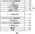
图4说明了根据本发明第四实施方案的基于氮化物的3-5族化合物半导体发光器件的结构。FIG. 4 illustrates the structure of a nitride-based Group 3-5 compound semiconductor light emitting device according to a fourth embodiment of the present invention.
具体实施方式Detailed ways
下面将参考附图详细说明本发明的优选实施方案。Preferred embodiments of the present invention will be described in detail below with reference to the accompanying drawings.
当本发明的优选实施方案在参考附图加以描述的同时,本领域技术人员可以看出:本发明的原理不但不受所公开的实施方案的限制,还可以通过增加、改变和省略一些部分而修改为各种替换方式。While the preferred embodiments of the present invention are described with reference to the accompanying drawings, those skilled in the art can see that the principle of the present invention is not limited to the disclosed embodiments, but can also be improved by adding, changing and omitting some parts. Modified into various alternatives.
第一实施方案first embodiment
图1说明了根据本发明第一实施方案的基于氮化物的3-5族化合物半导体发光器件的结构。FIG. 1 illustrates the structure of a nitride-based Group 3-5 compound semiconductor light emitting device according to a first embodiment of the present invention.
如图1所示,基于氮化物的3-5族化合物半导体发光器件具有包括下述的横截面结构:在衬底102上生长的缓冲层104、由n型GaN层(共掺杂有Si和In)组成的第一电极接触层108和InxGa1-xN/InyGa1-yN超晶格结构的第二电极接触层120。这里,第一和第二电极接触层108和120在下面的加工步骤中分别提供有电极(未示出),以便可以通过电极向其施加外部电压。As shown in FIG. 1 , a nitride-based group 3-5 compound semiconductor light emitting device has a cross-sectional structure comprising a
本发明的基于氮化物的3-5族化合物半导体发光器件还具有量子阱结构的有源层116,其置于第一电极接触层108和第二电极接触层120之间,形成异质结构。有源层116包括低摩尔In掺杂的GaN层110、InxGa1-yN阱层112和InxGa1-xN势垒层114。The nitride-based group 3-5 compound semiconductor light emitting device of the present invention also has an
另外,基于氮化物的3-5族化合物半导体发光器件还具有形成于缓冲层104和第一电极接触层108之间的In掺杂的GaN层106,和形成于InxGa1-xN势垒层114和第二电极接触层120之间的p型GaN层118。In addition, the nitride-based Group 3-5 compound semiconductor light emitting device also has an In-doped
本发明的基于氮化物的3-5族化合物半导体发光器件的制造方法如下所述:The manufacturing method of the nitride-based Group 3-5 compound semiconductor light-emitting device of the present invention is as follows:
首先,低生长温度下在蓝宝石衬底102上形成GaN缓冲层104。然后,低生长温度下GaN基半导体的缓冲层104可以生长成InGaN/GaN超晶格结构和InxGa1-xN/GaN与AlxInyGa1-x,yN/InxGa1-xN/GaN结构。First, a GaN
如上所述在衬底102上形成的缓冲层104可以有效地限制由衬底102和在衬底102上生长的GaN基单晶层之间的热膨胀系数失配和晶格常数失配所致的晶体缺陷,从而生成高质量的GaN基半导体。The
更具体地说,在生长GaN缓冲层104的加工步骤中,在约500-700℃的温度下供给H2与N2载气;TMGa、TMIn与TMA1源和NH3气体,以生长GaN缓冲层104。More specifically, in the process step of growing the
然后,高的生长温度下在缓冲层104上生长In掺杂的GaN层106和其中包含Si和In共掺杂的GaN层108。这里Si/In共掺杂的GaN层108用作第一电极接触层。Then, an In-doped
更具体地说,在生长GaN基半导体的GaN基单晶层的加工步骤中,通过在约900-1100℃的温度下供给MOCVD设备TMGa、TMIn和TMA1源来生长GaN基单晶层,其中SiH4气体可以用作Si掺杂源,TMIn可以用作In掺杂源。More specifically, in the processing step of growing a GaN-based single-crystal layer of a GaN-based semiconductor, the GaN-based single-crystal layer is grown by supplying sources of TMGa, TMIn, and TMA1 to an MOCVD apparatus at a temperature of about 900-1100° C., in which SiH 4 gas can be used as a Si doping source, and TMIn can be used as an In doping source.
发射所需波长范围内的光的有源层116包括单量子阱。更具体地说,有源层116的低摩尔In掺杂的GaN层110生长在10-500

在生长有源层116的单量子阱结构的加工步骤中,通过在NH3气氛中在N2或H2+N2载气上流动TMGa、TMIn和TMA1源,生长低摩尔In掺杂的InxGa1-xN层110、InyGa1-yN阱层112(0<y≤0.35)和InzGa1-zN势垒层114(0<z≤0.2)。在这种情况下,低摩尔In掺杂的InxGa1-xN层110具有约10-500


另外,为了实现高亮度发光器件性能,有必要从低摩尔In掺杂的InxGa1-xN层110表面到InGaN势垒层114维持均匀的螺旋模式。如果满足上述生长条件,可以通过形成具有单量子阱结构以及具有多量子阱结构的有源层来制造实用的高亮度发光器件。当然,在其他部分相同的情况下可以采用多量子阱结构。In addition, in order to achieve high-brightness light-emitting device performance, it is necessary to maintain a uniform helical pattern from the surface of the low-mole In-doped In x Ga 1-x
其间,低摩尔In掺杂的InxGa1-xN层110、InyGa1-yN阱层112和InzGa1-zN势垒层114中掺杂物的含量分布可以调整如下:低摩尔In掺杂的InxGa1-xN层110的In含量调整至低于InzGa1-zN势垒层114的In含量。掺杂的In含量x、y和z可以表示为0<x<0.05、0<y<0.3和0<z<0.1。Meanwhile, the content distribution of dopants in the low-mole In doped In x Ga 1-x N layer 110, In y Ga 1-y N well layer 112 and In z Ga 1-z
根据所述加工步骤生长发光的有源层之后,升高温度,在H2、N2和H2+N2气体中、NH3气氛下生长Mg掺杂的p型GaN基单晶层118。在约900-1020℃的生长温度下p型GaN层118生长至厚度约500-5000
在生长p型GaN层118时,InxGa1-xN/InyGa1-yN超晶格结构(0<x≤0.2和0<y≤0.2)的第二电极接触层120在p型GaN层118上生长。InxGa1-xN/InyGa1-yN超晶格结构赋予传播到第二电极接触层120的有效电流。第二电极接触层的电极可以从与第一电极接触层108相同的电极金属有利地获得。When growing the p-
根据该实施方案的基于氮化物的3-5族化合物半导体发光器件,第一电极接触层108由n型电极接触层形成,并且第二电极接触层120由n-型电极接触层形成。由于在具有n型和p型电极接触层形式的第一和第二电极接触层的常规基于氮化物的3-5族化合物半导体发光器件中,高接触阻抗缘于用作第二电极接触层的p型GaN层的低Mg掺杂效率,因此该实施方案可以克服高接触阻抗,除去所产生的电流传播层。According to the nitride-based Group 3-5 compound semiconductor light emitting device of this embodiment, the first
至于和p型GaN层118的关系,可以表示为第一电极接触层108、p型GaN层118和第二电极接触层120具有n-p-n连接。As for the relationship with the p-
这里,第二电极接触层120在2-50
第二实施方案second embodiment
图2说明了根据本发明的第二实施方案的基于氮化物的3-5族化合物半导体发光器件的结构。FIG. 2 illustrates the structure of a nitride-based Group 3-5 compound semiconductor light emitting device according to a second embodiment of the present invention.
本发明的如图2所示的基于氮化物的3-5族化合物半导体发光器件的结构与第一实施方案的基本相同,除了在第一电极接触层212之下还置有InxGa1-xN/InyGa1-yN超晶格结构层210以形成异质结构,以便使由衬底202和Si/In掺杂的GaN基单晶层212之间的晶格常数失配和热膨胀系数失配所致的晶体缺陷最小。The structure of the nitride-based Group 3-5 compound semiconductor light-emitting device of the present invention shown in FIG. 2 is basically the same as that of the first embodiment, except that In x Ga 1- x N/In y Ga 1-y N
该结构可以减小从衬底202和低温缓冲层204传播的位错密度,以提高发光器件的反击穿电压Vbr,从而提高其可靠性。This structure can reduce the density of dislocations propagating from the
根据本发明的第二个实施方案的基于氮化物的3-5族化合物半导体发光器件的结构将简要描述如下:The structure of the nitride-based Group 3-5 compound semiconductor light-emitting device according to the second embodiment of the present invention will be briefly described as follows:
缓冲层204在衬底202上生长,第一电极接触层212由n型GaN(共掺杂有Si和In)组成,第二电极接触层224生长成具有InxGa1-xN/InyGa1-yN超晶格结构。在下面的加工步骤中第一和第二电极接触层212、224分别提供有电极(未示出),以便可以通过电极向其施加外部电压。The
本发明的基于氮化物的3-5族化合物半导体发光器件还具有单量子阱结构的有源层220,其位于第一电极接触层212和第二电极接触层224之间,以形成异质结构。有源层220包括低摩尔In掺杂的InxGa1-xN层214、InxGa1-yN阱层216和InxGa1-xN势垒层218。The nitride-based Group 3-5 compound semiconductor light-emitting device of the present invention also has an
另外,基于氮化物的3-5族化合物半导体发光器件还具有In掺杂的GaN层206和未掺杂的GaN层208,位于缓冲层204和第一电极接触层212之间。在InxGa1-xN势垒层218和第二电极接触层224之间还形成p型GaN层222。In addition, the nitride-based group 3-5 compound semiconductor light emitting device further has an In-doped
具有上述结构的基于氮化物的3-5族化合物半导体发光器件的制造方法和第一实施方案类似,因此将不再进一步描述。The manufacturing method of the nitride-based Group 3-5 compound semiconductor light-emitting device having the above structure is similar to that of the first embodiment, and thus will not be further described.
这种结构的第二实施方案可以减小从衬底202和缓冲层204传播的位错密度,以提高发光器件的反击穿电压Vbr,从而提高其可靠性。The second embodiment of this structure can reduce the density of dislocations propagating from the
第三实施方案third embodiment
图3说明了根据本发明的第三实施方案的基于氮化物的3-5族化合物半导体发光器件的结构。FIG. 3 illustrates the structure of a nitride-based Group 3-5 compound semiconductor light emitting device according to a third embodiment of the present invention.
如图3所示,该实施方案与第一实施方案基本类似,除了在p型GaN层320和InzGa1-zN势垒层314之间还置有In掺杂的GaN层318,以形成异质结构。As shown in FIG. 3 , this embodiment is basically similar to the first embodiment, except that an In-doped
额外的In掺杂的GaN层318可以限制在p型GaN层320中用作掺杂物的Mg原子的向内扩散(in-diffusion),从而改善其特征。In掺杂的GaN层318生长至100
下面将描述第三实施方案的半导体发光器件的制造方法。在衬底302上生长缓冲层304,第一电极接触层308由n型GaN(共掺杂有Si和In)制成,第二电极接触层322由InxGa1-xN/InyGa1-yN超晶格结构形成。这里,在下面的加工步骤中第一和第二电极接触层308、322分别提供有电极(未示出),以便可以通过电极向其施加外部电压。A method of manufacturing the semiconductor light emitting device of the third embodiment will be described below. The
本发明的基于氮化物的3-5族化合物半导体发光器件还具有单量子阱结构的有源层316,其位于第一电极接触层308和第二电极接触层322之间,以形成异质结构。有源层316包括低摩尔In掺杂的InxGa1-xN层310、InxGa1-yN阱层312和InxGa1-xN势垒层314。The nitride-based Group 3-5 compound semiconductor light-emitting device of the present invention also has an
另外,基于氮化物的3-5族化合物半导体发光器件还具有位于缓冲层304和第一电极接触层308之间的In掺杂的GaN层306,并且p型GaN层320和In掺杂的GaN层318置于InzGa1-zN势垒层314与第二电极接触层322之间。In addition, the nitride-based Group 3-5 compound semiconductor light emitting device also has an In-doped
如上所述,该实施方案的额外GaN层318可以限制在p型GaN层320中用作掺杂物的Mg原子的向内扩散。该实施方案可以改善发光器件的特征。As mentioned above, the
第四实施方案Fourth Embodiment
图4说明了根据本发明的第四实施方案的基于氮化物的3-5族化合物半导体发光器件的结构。FIG. 4 illustrates the structure of a nitride-based Group 3-5 compound semiconductor light emitting device according to a fourth embodiment of the present invention.
第四实施方案的许多部分都和第三实施方案相同,除了额外提供In掺杂的GaN层406、InxGa1-xN/InyGa1-yN超晶格结构层408、In掺杂的GaN层412和InxGa1-xN/InyGa1-yN超晶格结构层414。InxGa1-xN/InyGa1-yN超晶格结构层408、In掺杂的GaN层412和InxGa1-xN/InyGa1-yN超晶格结构层414的作用是使来自衬底402的晶格常数失配和热膨胀系数失配的晶体缺陷最小化。另外,InxGa1-xN/InyGa1-yN超晶格结构层408还可以减小从衬底402和低温缓冲层404传播的位错密度,从而提高发光器件的反击穿电压Vbr。Many parts of the fourth embodiment are the same as the third embodiment, except that an In-doped
下面将参照图4来详细描述该实施方案的半导体发光器件的制造方法。A method of manufacturing the semiconductor light emitting device of this embodiment will be described in detail below with reference to FIG. 4 .
低的生长温度下在蓝宝石衬底402上生长GaN基半导体缓冲层404。在低的生长温度下,GaN基半导体的缓冲层404可以由InGaN/GaN超晶格结构和InxGa1-xN/GaN与AlxInyGa1-x,yN/InxGa1-xN/GaN的结构形成。A GaN-based
如上所述在衬底402上形成的缓冲层404可以有效地限制由衬底402和在衬底402上生长的GaN基单晶层之间的热膨胀系数失配和晶格常数失配所致的晶体缺陷,从而生成高质量的GaN基半导体。The
然后,高的生长温度下在缓冲层404上生长In掺杂的GaN层406,在In掺杂的GaN层406上还形成InxGa1-xN/InyGa1-yN超晶格结构层408,从而使来自衬底402的晶格常数失配和热膨胀系数失配的晶体缺陷最小化。Then, an In-doped
该结构可以减小从衬底402和低温缓冲层404传播的位错密度,以提高发光器件的反击穿电压Vbr,从而提高其可靠性。This structure can reduce the density of dislocations propagating from the
另外,在InxGa1-xN/InyGa1-yN超晶格结构层408上还形成In掺杂的GaN层412和InxGa1-xN/InyGa1-yN超晶格结构层414,以进一步减小晶体缺陷。In addition, an In-doped
然后,在InxGa1-xN/InyGa1-yN超晶格结构层414上生长Si/In共掺杂的GaN层416。Si/In共掺杂的GaN层416用作第一电极接触层。Then, a Si/In
随后,在有源层424中形成单量子阱层,用于发射所需波长范围的光。更具体地说,低摩尔In掺杂的InxGa1-xN层418(0<x≤0.2)首先在有源层424中生长,以提高有源层424的内部量子效率。在低摩尔In掺杂的InxGa1-xN层418上生长包括InyGa1-yN阱层420和不同In含量的InzGa1-zN势垒层422的量子阱结构,即得有源层。Subsequently, a single quantum well layer for emitting light in a desired wavelength range is formed in the
在生长步骤中,通过在NH3气氛中供给N2与H2+N2气体和TMGa、TMIn与TMA1源,生长单量子阱结构的有源层424,其包括低摩尔In掺杂的InxGa1-xN层418、InyGa1-yN阱层420(0<y≤0.35)和InzGa1-zN势垒层422(0<z≤0.2)。低摩尔InxGa1-xN层418具有约10-500
在约700-800℃的生长温度下,发光的InGaN阱层420生长至厚度为10-40

生长发光有源层后,生长In掺杂的GaN层426和Mg掺杂的p型GaN GaN基单晶层428。在约900-1020℃的生长温度下,p型GaN层428生长至厚度约为500-5000
然后,生长p型GaN层428后,在p型GaN层428上生长InxGa1-xN/InyGa1-yN超晶格结构(0<x≤0.2,且0<y≤0.2)的第二电极接触层430。有利的是,InxGa1-xN/InyGa1-yN超晶格结构可以完成第二电极接触层430的电流传播,第二电极接触层的电极可以从与第一电极接触层416相同的电极金属获得。Then, after growing the p-
根据该实施方案的基于氮化物的3-5族化合物半导体发光器件,第一电极接触层416由n型电极接触层形成,并且第二电极接触层430由n型电极接触层形成。由于在具有n型和p型电极接触层形式的第一和第二电极接触层的常规基于氮化物的3-5族化合物半导体发光器件中,高接触阻抗缘于用作第二电极接触层的p型GaN层的低Mg掺杂效率,因此该实施方案可以克服高接触阻抗,除去所产生的电流传播层。According to the nitride-based Group 3-5 compound semiconductor light emitting device of this embodiment, the first
至于和p型GaN层428的关系,可以表示为第一电极接触层416、p型GaN层428和第二电极接触层430具有n-p-n连接。第二电极接触层430的超晶格结构层在2-50的厚度下彼此交替,并且第二电极接触层430具有小于200的最大厚度。另外,在700-850℃的生长温度范围内,通过供给N2、N2+H2与NH3气体和TMGa与TMIn源进行生长步骤,以生长具有异质结构的高亮度发光器件,其在内部量子效率和工作电压性质方面是优异的。As for the relationship with the p-
工业应用性Industrial applicability
根据本发明的上述基于氮化物的3-5族化合物半导体发光器件及其制造方法,可以有效地限制由衬底如蓝宝石和在其上生长的GaN GaN基单晶层之间的热膨胀系数失配与晶格常数失配所致的晶体缺陷,从而生长高质量的GaN基半导体。具体是,InxGa1-xN/InyGa1-yN超晶格结构置于Si-In共掺杂的GaN层之下用作第一电极接触层,从而进一步限制晶体缺陷。According to the above-mentioned nitride-based Group 3-5 compound semiconductor light-emitting device and its manufacturing method of the present invention, it is possible to effectively limit the thermal expansion coefficient mismatch between a substrate such as sapphire and a GaN GaN-based single crystal layer grown thereon Crystal defects caused by lattice constant mismatch to grow high-quality GaN-based semiconductors. Specifically, the In x Ga 1-x N/In y Ga 1-y N superlattice structure is placed under the Si-In co-doped GaN layer as the first electrode contact layer, thereby further confining crystal defects.
另外,加入了低摩尔In掺杂的InxGa1-xN,以提高有源层的内部量子效率,从而均匀地控制量子阱的生长模式。由于InxGa1-xN/InyGa1-yN超晶格结构用作第二电极接触层,可以减小工作电压。结果,本发明可以有利地减小基于氮化物的3-5族化合物半导体发光器件的晶体缺陷,并提高GaN GaN基单晶层的结晶性,从而提高基于氮化物的3-5族化合物半导体发光器件的性能和可靠性。In addition, low-molar In-doped InxGa1 -xN was added to increase the internal quantum efficiency of the active layer, thereby uniformly controlling the growth mode of the quantum wells. Since the In x Ga 1-x N/In y Ga 1-y N superlattice structure is used as the second electrode contact layer, the operating voltage can be reduced. As a result, the present invention can advantageously reduce the crystal defects of the nitride-based Group 3-5 compound semiconductor light-emitting device, and improve the crystallinity of the GaN GaN-based single crystal layer, thereby improving the nitride-based Group 3-5 compound semiconductor light emission device performance and reliability.
Claims (25)
Applications Claiming Priority (3)
| Application Number | Priority Date | Filing Date | Title |
|---|---|---|---|
| KR10-2003-0041409A KR100525545B1 (en) | 2003-06-25 | 2003-06-25 | Nitride semiconductor LED and fabrication method for thereof |
| KR10-2003-0041409 | 2003-06-25 | ||
| KR1020030041409 | 2003-06-25 |
Related Parent Applications (1)
| Application Number | Title | Priority Date | Filing Date |
|---|---|---|---|
| CNB2004800003288A Division CN100468793C (en) | 2003-06-25 | 2004-06-21 | Light emitting device using nitride semiconductor and its manufacturing method |
Publications (2)
| Publication Number | Publication Date |
|---|---|
| CN101179106A CN101179106A (en) | 2008-05-14 |
| CN101179106B true CN101179106B (en) | 2013-01-23 |
Family
ID=36165438
Family Applications (2)
| Application Number | Title | Priority Date | Filing Date |
|---|---|---|---|
| CN200710196586.3A Expired - Fee Related CN101179106B (en) | 2003-06-25 | 2004-06-21 | A light emitting device using nitride semiconductor and fabrication method of the same |
| CNB2004800003288A Expired - Fee Related CN100468793C (en) | 2003-06-25 | 2004-06-21 | Light emitting device using nitride semiconductor and its manufacturing method |
Family Applications After (1)
| Application Number | Title | Priority Date | Filing Date |
|---|---|---|---|
| CNB2004800003288A Expired - Fee Related CN100468793C (en) | 2003-06-25 | 2004-06-21 | Light emitting device using nitride semiconductor and its manufacturing method |
Country Status (7)
| Country | Link |
|---|---|
| US (2) | US7193236B2 (en) |
| EP (1) | EP1636858B1 (en) |
| JP (2) | JP2006510234A (en) |
| KR (1) | KR100525545B1 (en) |
| CN (2) | CN101179106B (en) |
| DE (1) | DE202004021874U1 (en) |
| WO (1) | WO2004114421A1 (en) |
Families Citing this family (45)
| Publication number | Priority date | Publication date | Assignee | Title |
|---|---|---|---|---|
| KR100583163B1 (en) * | 2002-08-19 | 2006-05-23 | 엘지이노텍 주식회사 | Nitride Semiconductor and Manufacturing Method |
| KR100525545B1 (en) * | 2003-06-25 | 2005-10-31 | 엘지이노텍 주식회사 | Nitride semiconductor LED and fabrication method for thereof |
| KR100641989B1 (en) | 2003-10-15 | 2006-11-02 | 엘지이노텍 주식회사 | Nitride semiconductor light emitting device |
| KR100661708B1 (en) * | 2004-10-19 | 2006-12-26 | 엘지이노텍 주식회사 | Nitride semiconductor light emitting device and manufacturing method |
| US20060267043A1 (en) * | 2005-05-27 | 2006-11-30 | Emerson David T | Deep ultraviolet light emitting devices and methods of fabricating deep ultraviolet light emitting devices |
| KR100918968B1 (en) * | 2005-05-30 | 2009-09-25 | 갤럭시아포토닉스 주식회사 | Method for manufacturing gallium nitride device having a supercontact layer and device |
| US7847279B2 (en) * | 2005-07-06 | 2010-12-07 | Lg Innotek Co., Ltd. | Nitride semiconductor LED and fabrication method thereof |
| KR101241477B1 (en) | 2006-01-27 | 2013-03-08 | 엘지이노텍 주식회사 | Nitride semiconductor light-emitting device and manufacturing method thereof |
| EP1821347B1 (en) * | 2006-02-16 | 2018-01-03 | LG Electronics Inc. | Light emitting device having vertical structure and method for manufacturing the same |
| US20080149946A1 (en) * | 2006-12-22 | 2008-06-26 | Philips Lumileds Lighting Company, Llc | Semiconductor Light Emitting Device Configured To Emit Multiple Wavelengths Of Light |
| KR100910365B1 (en) * | 2007-06-11 | 2009-08-04 | 고려대학교 산학협력단 | Vertical nitride light emitting device and manufacturing method thereof |
| JP2009016467A (en) * | 2007-07-03 | 2009-01-22 | Sony Corp | Gallium nitride semiconductor device, optical device using the same, and image display device using the same |
| KR100864609B1 (en) * | 2007-07-04 | 2008-10-22 | 우리엘에스티 주식회사 | Light emitting device using compound semiconductor |
| KR100997908B1 (en) * | 2008-09-10 | 2010-12-02 | 박은현 | Group III nitride semiconductor light emitting device |
| US20100123119A1 (en) * | 2008-11-20 | 2010-05-20 | Seoul Opto Device Co., Ltd. | Light emitting diode having indium nitride |
| KR101507130B1 (en) * | 2008-11-20 | 2015-03-30 | 서울바이오시스 주식회사 | Light emitting diode having superlattice layer |
| US8992558B2 (en) | 2008-12-18 | 2015-03-31 | Osteomed, Llc | Lateral access system for the lumbar spine |
| DE102009040438A1 (en) * | 2009-07-24 | 2011-01-27 | Osram Opto Semiconductors Gmbh | Optoelectronic semiconductor body with a quantum well structure |
| KR101710892B1 (en) * | 2010-11-16 | 2017-02-28 | 엘지이노텍 주식회사 | Light-emitting device |
| KR101285527B1 (en) * | 2012-05-11 | 2013-07-17 | 엘지전자 주식회사 | Light emitting diode |
| KR102014172B1 (en) * | 2012-08-07 | 2019-08-26 | 엘지이노텍 주식회사 | Uv light emitting device and light emitting device package |
| JP6223075B2 (en) * | 2012-10-09 | 2017-11-01 | キヤノン株式会社 | Light emitting device manufacturing method and light emitting device |
| US10969805B2 (en) | 2013-02-11 | 2021-04-06 | Graco Minnesota Inc. | Paint sprayer distributed control and output volume monitoring architectures |
| EP2954504A4 (en) | 2013-02-11 | 2016-10-12 | Graco Minnesota Inc | Remote monitoring for fluid applicator system |
| TWI593135B (en) | 2013-03-15 | 2017-07-21 | 索泰克公司 | Semiconductor structure having an active region containing indium gallium nitride, a method of forming such a semiconductor structure, and a light-emitting element formed using the semiconductor structure |
| TWI648872B (en) | 2013-03-15 | 2019-01-21 | 法商梭意泰科公司 | Semiconductor structures having active regions comprising ingan, methods of forming such semiconductor structures, and light emitting devices formed from such semiconductor structures |
| CN105051918A (en) * | 2013-03-15 | 2015-11-11 | 索泰克公司 | Semiconductor structures having active regions comprising ingan, methods of forming such semiconductor structures, and light emitting devices formed from such semiconductor structures |
| FR3003397B1 (en) | 2013-03-15 | 2016-07-22 | Soitec Silicon On Insulator | Semiconductor structures with active regions including INGAN |
| KR20150132204A (en) * | 2013-03-15 | 2015-11-25 | 소이텍 | Semiconductor structures having active regions comprising ingan, methods of forming such semiconductor structures, and light emitting devices formed from such semiconductor structures |
| TWI626765B (en) * | 2013-03-15 | 2018-06-11 | 梭意泰科公司 | Semiconductor structures having active regions comprising ingan, methods of forming such semiconductor structures, and light emitting devices formed from such semiconductor structures |
| CN103779467A (en) * | 2014-01-14 | 2014-05-07 | 江苏新广联科技股份有限公司 | Epitaxial PGaN-layer growth structure capable of improving light-emitting efficiency |
| CN104300047B (en) * | 2014-10-11 | 2017-06-23 | 华芯半导体科技有限公司 | A kind of LED structure of Si bases GaN and preparation method thereof |
| CN105355741B (en) * | 2015-11-02 | 2017-09-29 | 厦门市三安光电科技有限公司 | A kind of LED epitaxial structure and preparation method |
| EP3503814B1 (en) | 2016-08-23 | 2024-07-10 | Stryker European Operations Holdings LLC | Instrumentation for the implantation of spinal implants |
| CN106856217A (en) * | 2016-12-27 | 2017-06-16 | 圆融光电科技股份有限公司 | The growing method of N-type superlattices contact layer |
| CN107195736B (en) * | 2017-05-27 | 2019-12-31 | 华灿光电(浙江)有限公司 | A gallium nitride-based light-emitting diode epitaxial wafer and its growth method |
| US10372363B2 (en) * | 2017-09-14 | 2019-08-06 | International Business Machines Corporation | Thin provisioning using cloud based ranks |
| JPWO2019188318A1 (en) * | 2018-03-26 | 2021-04-08 | パナソニック株式会社 | Semiconductor light emitting device |
| EP3545857B1 (en) | 2018-03-30 | 2024-01-03 | Stryker European Operations Holdings LLC | Lateral access retractor and core insertion |
| JP2020021798A (en) * | 2018-07-31 | 2020-02-06 | 日機装株式会社 | Nitride semiconductor light emitting device and method of manufacturing the same |
| WO2020248098A1 (en) * | 2019-06-10 | 2020-12-17 | 苏州晶湛半导体有限公司 | Semiconductor structure and manufacturing method for semiconductor structure |
| CN110707187B (en) * | 2019-08-21 | 2021-01-29 | 华灿光电(苏州)有限公司 | Epitaxial wafer of small-spacing light-emitting diode and manufacturing method thereof |
| US11564674B2 (en) | 2019-11-27 | 2023-01-31 | K2M, Inc. | Lateral access system and method of use |
| CN117457824B (en) * | 2023-12-25 | 2024-03-12 | 江西兆驰半导体有限公司 | Light-emitting diode epitaxial wafer and preparation method thereof |
| CN117476827B (en) * | 2023-12-25 | 2024-04-26 | 江西兆驰半导体有限公司 | An epitaxial wafer of a light-emitting diode with low contact resistance and a method for preparing the same |
Family Cites Families (33)
| Publication number | Priority date | Publication date | Assignee | Title |
|---|---|---|---|---|
| JP2828002B2 (en) * | 1995-01-19 | 1998-11-25 | 松下電器産業株式会社 | Semiconductor light emitting device and method of manufacturing the same |
| DE69602141T2 (en) * | 1995-08-28 | 1999-10-21 | Mitsubishi Cable Industries, Ltd. | Group III nitride compound light emitting device |
| JPH09232629A (en) * | 1996-02-26 | 1997-09-05 | Toshiba Corp | Semiconductor element |
| JPH09304272A (en) * | 1996-05-10 | 1997-11-28 | Fuji Electric Co Ltd | Liquid absorbance measuring device |
| JP3753793B2 (en) * | 1996-06-14 | 2006-03-08 | 豊田合成株式会社 | Group 3 nitride compound semiconductor light emitting device |
| JPH10189944A (en) * | 1996-12-24 | 1998-07-21 | Furukawa Electric Co Ltd:The | High electron mobility transistor |
| US6677619B1 (en) * | 1997-01-09 | 2004-01-13 | Nichia Chemical Industries, Ltd. | Nitride semiconductor device |
| JPH10214999A (en) | 1997-01-30 | 1998-08-11 | Toyota Central Res & Dev Lab Inc | III-V nitride semiconductor device |
| JPH10303458A (en) * | 1997-04-24 | 1998-11-13 | Toyoda Gosei Co Ltd | Gallium nitride compound semiconductor element |
| US6266355B1 (en) * | 1997-09-12 | 2001-07-24 | Sdl, Inc. | Group III-V nitride laser devices with cladding layers to suppress defects such as cracking |
| JP3080155B2 (en) * | 1997-11-05 | 2000-08-21 | サンケン電気株式会社 | Semiconductor device having gallium nitride semiconductor layer and method of manufacturing the same |
| CA2322490C (en) | 1998-03-12 | 2010-10-26 | Nichia Chemical Industries, Ltd. | Nitride semiconductor device |
| JP3680558B2 (en) * | 1998-05-25 | 2005-08-10 | 日亜化学工業株式会社 | Nitride semiconductor device |
| US6194742B1 (en) * | 1998-06-05 | 2001-02-27 | Lumileds Lighting, U.S., Llc | Strain engineered and impurity controlled III-V nitride semiconductor films and optoelectronic devices |
| US6608330B1 (en) * | 1998-09-21 | 2003-08-19 | Nichia Corporation | Light emitting device |
| US6838705B1 (en) * | 1999-03-29 | 2005-01-04 | Nichia Corporation | Nitride semiconductor device |
| JP3551101B2 (en) * | 1999-03-29 | 2004-08-04 | 日亜化学工業株式会社 | Nitride semiconductor device |
| JP3763701B2 (en) * | 1999-05-17 | 2006-04-05 | 株式会社東芝 | Gallium nitride semiconductor light emitting device |
| JP3719047B2 (en) * | 1999-06-07 | 2005-11-24 | 日亜化学工業株式会社 | Nitride semiconductor device |
| JP3609661B2 (en) * | 1999-08-19 | 2005-01-12 | 株式会社東芝 | Semiconductor light emitting device |
| JP3497790B2 (en) * | 1999-11-29 | 2004-02-16 | 星和電機株式会社 | Method for manufacturing p-type gallium nitride based semiconductor and light emitting device using p-type gallium nitride based semiconductor |
| JP2001185493A (en) * | 1999-12-24 | 2001-07-06 | Toyoda Gosei Co Ltd | Method of manufacturing group III nitride compound semiconductor and group III nitride compound semiconductor device |
| JP3925066B2 (en) | 2000-09-28 | 2007-06-06 | 日亜化学工業株式会社 | Nitride semiconductor laser device |
| US6906352B2 (en) * | 2001-01-16 | 2005-06-14 | Cree, Inc. | Group III nitride LED with undoped cladding layer and multiple quantum well |
| TW493287B (en) * | 2001-05-30 | 2002-07-01 | Epistar Corp | Light emitting diode structure with non-conductive substrate |
| US6958497B2 (en) * | 2001-05-30 | 2005-10-25 | Cree, Inc. | Group III nitride based light emitting diode structures with a quantum well and superlattice, group III nitride based quantum well structures and group III nitride based superlattice structures |
| CN101834245B (en) * | 2001-06-15 | 2013-05-22 | 克里公司 | GaN-based LEDs formed on SiC substrates |
| JP2003110197A (en) * | 2001-09-28 | 2003-04-11 | Toshiba Corp | Nitride semiconductor light emission device, nitride semiconductor device and method for manufacturing the same |
| US6833564B2 (en) * | 2001-11-02 | 2004-12-21 | Lumileds Lighting U.S., Llc | Indium gallium nitride separate confinement heterostructure light emitting devices |
| JP4150527B2 (en) | 2002-02-27 | 2008-09-17 | 日鉱金属株式会社 | Crystal production method |
| US6720570B2 (en) * | 2002-04-17 | 2004-04-13 | Tekcore Co., Ltd. | Gallium nitride-based semiconductor light emitting device |
| US7058105B2 (en) * | 2002-10-17 | 2006-06-06 | Samsung Electro-Mechanics Co., Ltd. | Semiconductor optoelectronic device |
| KR100525545B1 (en) * | 2003-06-25 | 2005-10-31 | 엘지이노텍 주식회사 | Nitride semiconductor LED and fabrication method for thereof |
-
2003
- 2003-06-25 KR KR10-2003-0041409A patent/KR100525545B1/en not_active IP Right Cessation
-
2004
- 2004-06-21 EP EP04737100.0A patent/EP1636858B1/en not_active Expired - Lifetime
- 2004-06-21 CN CN200710196586.3A patent/CN101179106B/en not_active Expired - Fee Related
- 2004-06-21 WO PCT/KR2004/001480 patent/WO2004114421A1/en active Application Filing
- 2004-06-21 US US10/517,819 patent/US7193236B2/en not_active Expired - Lifetime
- 2004-06-21 JP JP2005518142A patent/JP2006510234A/en active Pending
- 2004-06-21 CN CNB2004800003288A patent/CN100468793C/en not_active Expired - Fee Related
- 2004-06-21 DE DE202004021874U patent/DE202004021874U1/en not_active Expired - Lifetime
-
2005
- 2005-11-29 US US11/288,310 patent/US7691657B2/en not_active Expired - Lifetime
-
2008
- 2008-04-22 JP JP2008111431A patent/JP2008182284A/en active Pending
Also Published As
| Publication number | Publication date |
|---|---|
| WO2004114421A1 (en) | 2004-12-29 |
| US20050236631A1 (en) | 2005-10-27 |
| CN100468793C (en) | 2009-03-11 |
| KR20050000846A (en) | 2005-01-06 |
| EP1636858B1 (en) | 2016-11-16 |
| US20060081831A1 (en) | 2006-04-20 |
| JP2008182284A (en) | 2008-08-07 |
| US7193236B2 (en) | 2007-03-20 |
| CN101179106A (en) | 2008-05-14 |
| JP2006510234A (en) | 2006-03-23 |
| EP1636858A1 (en) | 2006-03-22 |
| DE202004021874U1 (en) | 2012-01-18 |
| US7691657B2 (en) | 2010-04-06 |
| EP1636858A4 (en) | 2007-01-24 |
| CN1698212A (en) | 2005-11-16 |
| KR100525545B1 (en) | 2005-10-31 |
Similar Documents
| Publication | Publication Date | Title |
|---|---|---|
| CN101179106B (en) | A light emitting device using nitride semiconductor and fabrication method of the same | |
| CN111063777B (en) | Semiconductor device with a semiconductor device having a plurality of semiconductor chips | |
| CN100350639C (en) | Nitride semiconductor LED and fabrication method thereof | |
| JP3778344B2 (en) | Method for manufacturing light-emitting semiconductor device | |
| JP2006510234A5 (en) | ||
| KR101001527B1 (en) | Epitaxial Substrates for Compound Semiconductor Light-Emitting Devices, Manufacturing Method Thereof and Light-Emitting Devices | |
| CN110718612B (en) | Light-emitting diode epitaxial wafer and manufacturing method thereof | |
| CN102576782B (en) | There is light-emitting diode and the manufacture method thereof in the intermediate layer of high dislocation density | |
| CN110233190B (en) | Light emitting device | |
| KR100931509B1 (en) | Nitride semiconductor light emitting device and manufacturing method | |
| CN103996769B (en) | LED epitaxial layer structures, growing method and the LED chip with the structure | |
| CN113675303A (en) | Nitride light-emitting diode epitaxial wafer and preparation method thereof | |
| CN108831974A (en) | A light-emitting diode epitaxial wafer and its manufacturing method | |
| KR20060044241A (en) | Nitride semiconductor light emitting device and manufacturing method | |
| CN116598396A (en) | LED epitaxial wafer, preparation method thereof and LED | |
| CN103872204A (en) | P (Positive) type insert layer with cycle structure and growing method | |
| KR100318289B1 (en) | III-nitride semiconductor light emitting device | |
| CN109473525B (en) | A kind of gallium nitride-based light-emitting diode epitaxial wafer and manufacturing method thereof | |
| CN118782704B (en) | Light-emitting diode epitaxial wafer, preparation method thereof and light-emitting diode | |
| KR100616631B1 (en) | Nitride semiconductor light emitting device and its manufacturing method | |
| JP2004363349A (en) | Nitride system compound semiconductor device and light emitting device | |
| KR100974789B1 (en) | Gallium nitride based semiconductor device and manufacturing method thereof | |
| JP2005294867A (en) | Manufacturing method of nitride semiconductor device, and nitride semiconductor device |
Legal Events
| Date | Code | Title | Description |
|---|---|---|---|
| C06 | Publication | ||
| PB01 | Publication | ||
| C10 | Entry into substantive examination | ||
| SE01 | Entry into force of request for substantive examination | ||
| C12 | Rejection of a patent application after its publication | ||
| RJ01 | Rejection of invention patent application after publication |
Open date: 20080514 |
|
| CI01 | Publication of corrected invention patent application |
Correction item: Rejection of patent application Correct: Dismiss False: Reject Number: 32 Volume: 26 |
|
| ERR | Gazette correction |
Free format text: CORRECT: PATENT APPLICATION REJECTION OF AFTER PUBLICATION; FROM: REJECTION TO: REVOCATION REJECTED |
|
| C14 | Grant of patent or utility model | ||
| GR01 | Patent grant | ||
| CF01 | Termination of patent right due to non-payment of annual fee | ||
| CF01 | Termination of patent right due to non-payment of annual fee |
Granted publication date: 20130123 Termination date: 20170621 |