CN101089939A - Gate driving circuit and display device having the gate driving circuit - Google Patents
Gate driving circuit and display device having the gate driving circuit Download PDFInfo
- Publication number
- CN101089939A CN101089939A CNA200710108992XA CN200710108992A CN101089939A CN 101089939 A CN101089939 A CN 101089939A CN A200710108992X A CNA200710108992X A CN A200710108992XA CN 200710108992 A CN200710108992 A CN 200710108992A CN 101089939 A CN101089939 A CN 101089939A
- Authority
- CN
- China
- Prior art keywords
- load
- transistor
- pull
- node
- clock
- Prior art date
- Legal status (The legal status is an assumption and is not a legal conclusion. Google has not performed a legal analysis and makes no representation as to the accuracy of the status listed.)
- Granted
Links
- 230000002265 prevention Effects 0.000 claims abstract description 93
- 230000004044 response Effects 0.000 claims abstract description 64
- 239000003990 capacitor Substances 0.000 claims description 30
- 239000004973 liquid crystal related substance Substances 0.000 claims description 19
- 239000000758 substrate Substances 0.000 claims description 11
- 239000010409 thin film Substances 0.000 claims description 5
- 238000010586 diagram Methods 0.000 description 28
- 101100112673 Rattus norvegicus Ccnd2 gene Proteins 0.000 description 12
- 238000000034 method Methods 0.000 description 3
- 230000002093 peripheral effect Effects 0.000 description 3
- 238000012986 modification Methods 0.000 description 2
- 230000004048 modification Effects 0.000 description 2
- 230000008569 process Effects 0.000 description 2
- 238000012360 testing method Methods 0.000 description 2
- 230000007704 transition Effects 0.000 description 2
- 101000974356 Homo sapiens Nuclear receptor coactivator 3 Proteins 0.000 description 1
- 101000912503 Homo sapiens Tyrosine-protein kinase Fgr Proteins 0.000 description 1
- 102100037226 Nuclear receptor coactivator 2 Human genes 0.000 description 1
- 102100022883 Nuclear receptor coactivator 3 Human genes 0.000 description 1
- 230000008901 benefit Effects 0.000 description 1
- 230000007257 malfunction Effects 0.000 description 1
- 239000011159 matrix material Substances 0.000 description 1
Images


Classifications
-
- G—PHYSICS
- G09—EDUCATION; CRYPTOGRAPHY; DISPLAY; ADVERTISING; SEALS
- G09G—ARRANGEMENTS OR CIRCUITS FOR CONTROL OF INDICATING DEVICES USING STATIC MEANS TO PRESENT VARIABLE INFORMATION
- G09G3/00—Control arrangements or circuits, of interest only in connection with visual indicators other than cathode-ray tubes
- G09G3/20—Control arrangements or circuits, of interest only in connection with visual indicators other than cathode-ray tubes for presentation of an assembly of a number of characters, e.g. a page, by composing the assembly by combination of individual elements arranged in a matrix no fixed position being assigned to or needed to be assigned to the individual characters or partial characters
- G09G3/34—Control arrangements or circuits, of interest only in connection with visual indicators other than cathode-ray tubes for presentation of an assembly of a number of characters, e.g. a page, by composing the assembly by combination of individual elements arranged in a matrix no fixed position being assigned to or needed to be assigned to the individual characters or partial characters by control of light from an independent source
- G09G3/36—Control arrangements or circuits, of interest only in connection with visual indicators other than cathode-ray tubes for presentation of an assembly of a number of characters, e.g. a page, by composing the assembly by combination of individual elements arranged in a matrix no fixed position being assigned to or needed to be assigned to the individual characters or partial characters by control of light from an independent source using liquid crystals
- G09G3/3611—Control of matrices with row and column drivers
- G09G3/3674—Details of drivers for scan electrodes
- G09G3/3677—Details of drivers for scan electrodes suitable for active matrices only
-
- H—ELECTRICITY
- H03—ELECTRONIC CIRCUITRY
- H03K—PULSE TECHNIQUE
- H03K19/00—Logic circuits, i.e. having at least two inputs acting on one output; Inverting circuits
- H03K19/01—Modifications for accelerating switching
- H03K19/017—Modifications for accelerating switching in field-effect transistor circuits
- H03K19/01728—Modifications for accelerating switching in field-effect transistor circuits in synchronous circuits, i.e. by using clock signals
- H03K19/01742—Modifications for accelerating switching in field-effect transistor circuits in synchronous circuits, i.e. by using clock signals by means of a pull-up or down element
-
- G—PHYSICS
- G09—EDUCATION; CRYPTOGRAPHY; DISPLAY; ADVERTISING; SEALS
- G09G—ARRANGEMENTS OR CIRCUITS FOR CONTROL OF INDICATING DEVICES USING STATIC MEANS TO PRESENT VARIABLE INFORMATION
- G09G2310/00—Command of the display device
- G09G2310/02—Addressing, scanning or driving the display screen or processing steps related thereto
- G09G2310/0264—Details of driving circuits
- G09G2310/0278—Details of driving circuits arranged to drive both scan and data electrodes
-
- G—PHYSICS
- G09—EDUCATION; CRYPTOGRAPHY; DISPLAY; ADVERTISING; SEALS
- G09G—ARRANGEMENTS OR CIRCUITS FOR CONTROL OF INDICATING DEVICES USING STATIC MEANS TO PRESENT VARIABLE INFORMATION
- G09G2310/00—Command of the display device
- G09G2310/08—Details of timing specific for flat panels, other than clock recovery
Landscapes
- Engineering & Computer Science (AREA)
- Physics & Mathematics (AREA)
- Computer Hardware Design (AREA)
- Chemical & Material Sciences (AREA)
- Crystallography & Structural Chemistry (AREA)
- General Physics & Mathematics (AREA)
- Theoretical Computer Science (AREA)
- Computing Systems (AREA)
- General Engineering & Computer Science (AREA)
- Mathematical Physics (AREA)
- Control Of Indicators Other Than Cathode Ray Tubes (AREA)
Abstract
本发明公开了一种栅极驱动电路和具有该栅极驱动电路的显示装置,该栅极驱动电路包括在一帧内的第一时间段内分别将当前栅极信号和当前负载信号上拉至第一时钟的上拉部分和负载部分。下拉部分接收下一栅极信号,以将当前栅极信号放电至电源电压。上拉驱动部分连接到负载部分和上拉部分的控制端(Q节点),以导通和截止负载部分和上拉部分。在一帧内的第二时间段内,浮置防止部分响应第一时钟来防止负载部分的输出端浮置。
The invention discloses a gate driving circuit and a display device having the gate driving circuit. The gate driving circuit includes pulling up the current gate signal and the current load signal to The pull-up and load sections of the first clock. The pull-down part receives the next gate signal to discharge the current gate signal to the supply voltage. The pull-up driving part is connected to the control terminal (Q node) of the load part and the pull-up part to turn on and off the load part and the pull-up part. The floating prevention section prevents the output terminal of the load section from floating in response to the first clock during a second period of time within one frame.
Description
本申请要求于2006年6月12日提交的第2006-52610号和于2006年12月20日提交的第2006-131087号韩国专利申请的优先权和权益,其公开通过所有目的的引用包含于此,就像在此提出一样。This application claims priority and benefit from Korean Patent Applications No. 2006-52610 filed on June 12, 2006 and Korean Patent Application No. 2006-131087 filed on December 20, 2006, the disclosures of which are incorporated by reference for all purposes at Here, as proposed here.
技术领域technical field
本发明涉及一种栅极驱动电路和具有该栅极驱动电路的显示装置。更具体地讲,本发明涉及一种可以在高温操作的过程中可靠性得到提高的栅极驱动电路以及具有该栅极驱动电路的显示装置。The invention relates to a gate drive circuit and a display device with the gate drive circuit. More particularly, the present invention relates to a gate driving circuit whose reliability can be improved during high temperature operation and a display device having the gate driving circuit.
背景技术Background technique
通常,液晶显示装置包括用于显示图像的液晶显示面板,液晶显示面板具有下基底、与下基底面对的上基底以及置于上下基底之间的液晶层。Generally, a liquid crystal display device includes a liquid crystal display panel for displaying images, the liquid crystal display panel having a lower substrate, an upper substrate facing the lower substrate, and a liquid crystal layer interposed between the upper and lower substrates.
液晶显示面板包括多条栅极线、多条数据线和连接到栅极线和数据线的多个像素。向栅极线提供栅极信号的栅极驱动电路可以通过薄膜工艺直接形成在液晶显示面板上。A liquid crystal display panel includes a plurality of gate lines, a plurality of data lines, and a plurality of pixels connected to the gate lines and the data lines. A gate driving circuit that supplies gate signals to the gate lines can be directly formed on the liquid crystal display panel through a thin film process.
通常,栅极驱动电路可包括移位寄存器,在移位寄存器中,多个级串联连接。每个级包括多个晶体管,以向栅极线中对应的栅极线施加栅极电压。具体地讲,每个级可包括上拉(pull-up)晶体管和负载(carry)晶体管,其中,上拉晶体管连接到栅极线以输出栅极电压,负载晶体管连接到下一级的输入端以输出用于控制下一级驱动的负载电压。因此,栅极驱动电路可以防止由连接到栅极线的负载造成的失真信号被施加到下一级,从而防止了其误操作。Typically, a gate drive circuit may include a shift register in which a plurality of stages are connected in series. Each stage includes a plurality of transistors to apply a gate voltage to a corresponding one of the gate lines. Specifically, each stage may include a pull-up transistor and a load transistor, wherein the pull-up transistor is connected to the gate line to output the gate voltage, and the load transistor is connected to the input terminal of the next stage. To output the load voltage used to control the next stage drive. Therefore, the gate driving circuit can prevent a distorted signal caused by a load connected to the gate line from being applied to the next stage, thereby preventing its erroneous operation.
上拉晶体管和负载晶体管的控制端可以共同连接到每个级中的Q节点。在栅极电压和负载电压保持在低状态的(n-1)H时间段内,Q节点具有低于阈值电压的截止电压的电势。另一方面,在栅极电压和负载电压保持在高状态的1H时间段(一个水平扫描时间段)内,Q节点具有高于阈值电压的导通电压的电势。The control terminals of the pull-up and load transistors can be commonly connected to the Q-node in each stage. During the (n−1)H period in which the gate voltage and the load voltage are kept in the low state, the Q node has a potential of a cut-off voltage lower than the threshold voltage. On the other hand, during the 1H period (one horizontal scanning period) in which the gate voltage and the load voltage are kept in a high state, the Q node has a potential of an on-voltage higher than the threshold voltage.
然而,在(n-1)H时间段的预定时间段内,Q节点的电势会浮置(float)。因此,当Q节点的电势没有保持在截止电压时,上拉晶体管和负载晶体管可导通,从而造成栅极电压和负载电压的波纹(ripple)。具体地讲,当在高温条件下测试液晶显示面板时上拉晶体管和负载晶体管的电流特性变化时,会由于通过浮置的Q节点施加的噪声而造成栅极驱动电路的误操作,从而使栅极驱动电路的高温可靠性劣化。However, the potential of the Q node may float during a predetermined period of the (n−1)H period. Therefore, when the potential of the Q node is not maintained at the cut-off voltage, the pull-up transistor and the load transistor may be turned on, causing ripples in the gate voltage and the load voltage. Specifically, when the current characteristics of pull-up transistors and load transistors vary when testing liquid crystal display panels under high-temperature conditions, gate drive circuits may malfunction due to noise applied through the floating Q-node, causing gate The high-temperature reliability of the pole drive circuit deteriorates.
发明内容Contents of the invention
本发明提供了一种栅极驱动电路,该栅极驱动电路能够提高其高温可靠性并防止了误操作。The present invention provides a gate drive circuit capable of improving its high-temperature reliability and preventing misoperation.
本发明还提供了一种具有上述栅极驱动电路的显示装置。The present invention also provides a display device having the above-mentioned gate driving circuit.
本发明的附加特征将在随后的说明书中提出,并且部分地将从说明中清楚,或者可通过本发明的实践而得知。Additional features of the invention will be set forth in the description which follows, and in part will be apparent from the description, or may be learned by practice of the invention.
本发明公开了一种包括彼此串联连接的多级的栅极驱动电路。每个级包括上拉部分、负载部分、下拉部分、上拉驱动部分和浮置防止部分。上拉部分在一帧内的第一时间段内将当前栅极信号上拉至第一时钟,负载部分在所述第一时间段内将当前负载信号上拉至所述第一时钟。下拉部分从下一级接收下一栅极信号,以将所述当前栅极信号放电至电源电压。上拉驱动部分连接到Q节点,所述Q节点包括所述负载部分和所述上拉部分的控制端。上拉驱动部分从前一级接收前一负载信号,以响应下一栅极信号来导通和截止所述上拉部分和所述负载部分。浮置防止部分在一帧内的第二时间段内响应所述第一时钟向包括所述负载部分的输出端的当前负载节点提供所述当前栅极信号,并将所述当前负载节点复位,以防止下一级的Q节点浮置。所述第二时间段不包括所述第一时间段。The invention discloses a gate drive circuit comprising multiple stages connected in series. Each stage includes a pull-up section, a load section, a pull-down section, a pull-up driving section, and a floating prevention section. The pull-up part pulls up the current gate signal to the first clock within a first time period within a frame, and the load part pulls up the current load signal to the first clock within the first time period. The pull-down part receives the next gate signal from the next stage to discharge the current gate signal to the power supply voltage. The pull-up driving part is connected to a Q node, and the Q node includes the load part and a control terminal of the pull-up part. The pull-up driving part receives a previous load signal from a previous stage to turn on and off the pull-up part and the load part in response to a next gate signal. The floating prevention section supplies the current gate signal to a current load node including an output terminal of the load section in response to the first clock within a second period of time within one frame, and resets the current load node to Prevents the Q-node of the next stage from floating. The second time period does not include the first time period.
本发明还公开了一种包括彼此串联连接的多个级的栅极驱动电路。每个级包括上拉部分、负载部分、下拉部分、上拉驱动部分和浮置防止部分。上拉部分在一帧内的第一时间段内将当前栅极信号上拉至第一时钟,负载部分在所述第一时间段内将当前负载信号上拉至所述第一时钟。下拉部分从下一级接收下一栅极信号,以将所述当前栅极信号放电至第一电源电压。上拉驱动部分连接到Q节点,所述Q节点包括所述负载部分的控制端和所述上拉部分的控制端。上拉驱动部分从前一级接收前一负载信号,以响应下一栅极信号来导通和截止所述上拉部分和所述负载部分。浮置防止部分在一帧内的第二时间段内响应所述第一时钟向包括所述负载部分的输出端的当前负载节点提供小于所述第一电源电压的第二电源电压,以将所述当前负载信号下拉到所述第二电源电压。所述第二时间段不包括所述第一时间段。The present invention also discloses a gate driving circuit including a plurality of stages connected to each other in series. Each stage includes a pull-up section, a load section, a pull-down section, a pull-up driving section, and a floating prevention section. The pull-up part pulls up the current gate signal to the first clock within a first time period within a frame, and the load part pulls up the current load signal to the first clock within the first time period. The pull-down part receives a next gate signal from a next stage to discharge the current gate signal to the first power supply voltage. The pull-up driving part is connected to a Q node, and the Q node includes a control terminal of the load part and a control terminal of the pull-up part. The pull-up driving part receives a previous load signal from a previous stage to turn on and off the pull-up part and the load part in response to a next gate signal. The floating preventing section supplies a second power supply voltage smaller than the first power supply voltage to a current load node including an output terminal of the load section in response to the first clock for a second period of time within one frame, so that the The current load signal is pulled down to the second supply voltage. The second time period does not include the first time period.
本发明还公开了一种显示装置,该显示装置包括:显示部分,用于响应栅极信号和数据信号来显示图像;数据驱动电路,向所述显示部分施加所述数据信号;栅极驱动电路,包括彼此串联连接的多个级,以顺序地向所述显示部分输出所述栅极信号。所述栅极驱动电路的每个级包括上拉部分、负载部分、下拉部分、上拉驱动部分和浮置防止部分。上拉部分在一帧内的第一时间段内将当前栅极信号上拉至第一时钟,负载部分在所述第一时间段内将当前负载信号上拉至所述第一时钟。下拉部分从下一级接收下一栅极信号,以将所述当前栅极信号放电至电源电压。上拉驱动部分连接到Q节点,所述Q节点包括所述负载部分的控制端和所述上拉部分的控制端。上拉驱动部分从前一级接收前一负载信号,以响应下一栅极信号来导通和截止所述上拉部分和所述负载部分。浮置防止部分在一帧内的第二时间段内响应所述第一时钟向包括所述负载部分的输出端的当前负载节点提供所述当前栅极信号,并将所述当前负载节点复位,以防止下一级的Q节点浮置。所述第二时间段不包括所述第一时间段。The present invention also discloses a display device, which includes: a display part for displaying an image in response to a gate signal and a data signal; a data drive circuit for applying the data signal to the display part; a gate drive circuit , including a plurality of stages connected to each other in series to sequentially output the gate signal to the display portion. Each stage of the gate driving circuit includes a pull-up section, a load section, a pull-down section, a pull-up driving section, and a floating prevention section. The pull-up part pulls up the current gate signal to the first clock within a first time period within a frame, and the load part pulls up the current load signal to the first clock within the first time period. The pull-down part receives the next gate signal from the next stage to discharge the current gate signal to the power supply voltage. The pull-up driving part is connected to a Q node, and the Q node includes a control terminal of the load part and a control terminal of the pull-up part. The pull-up driving part receives a previous load signal from a previous stage to turn on and off the pull-up part and the load part in response to a next gate signal. The floating prevention section supplies the current gate signal to a current load node including an output terminal of the load section in response to the first clock within a second period of time within one frame, and resets the current load node to Prevents the Q-node of the next stage from floating. The second time period does not include the first time period.
本发明还公开了一种显示装置,该显示装置包括:显示部分,用于响应栅极信号和数据信号来显示图像;数据驱动电路,向所述显示部分施加所述数据信号;栅极驱动电路,包括彼此串联连接的多个级,以顺序地向所述显示部分输出所述栅极信号。所述栅极驱动电路的每个级包括上拉部分、负载部分、下拉部分、上拉驱动部分和浮置防止部分。上拉部分在一帧内的第一时间段内将当前栅极信号上拉至第一时钟,负载部分在所述第一时间段内将当前负载信号上拉至所述第一时钟。下拉部分从下一级接收下一栅极信号,以将所述当前栅极信号放电至第一电源电压。上拉驱动部分连接到Q节点,所述Q节点包括所述负载部分的控制端和所述上拉部分的控制端。上拉驱动部分从前一级接收前一负载信号,以响应下一栅极信号来导通和截止所述上拉部分和所述负载部分。浮置防止部分在一帧内的第二时间段内响应所述第一时钟向包括所述负载部分的输出端的当前负载节点提供小于所述第一电源电压的第二电源电压,并将所述当前负载信号下拉到所述第二电源电压。所述第二时间段不包括所述第一时间段。The present invention also discloses a display device, which includes: a display part for displaying an image in response to a gate signal and a data signal; a data drive circuit for applying the data signal to the display part; a gate drive circuit , including a plurality of stages connected to each other in series to sequentially output the gate signal to the display portion. Each stage of the gate driving circuit includes a pull-up section, a load section, a pull-down section, a pull-up driving section, and a floating prevention section. The pull-up part pulls up the current gate signal to the first clock within a first time period within a frame, and the load part pulls up the current load signal to the first clock within the first time period. The pull-down part receives a next gate signal from a next stage to discharge the current gate signal to the first power supply voltage. The pull-up driving part is connected to a Q node, and the Q node includes a control terminal of the load part and a control terminal of the pull-up part. The pull-up driving part receives a previous load signal from a previous stage to turn on and off the pull-up part and the load part in response to a next gate signal. The floating prevention section supplies a second power supply voltage smaller than the first power supply voltage to a current load node including an output terminal of the load section in response to the first clock for a second period of time within one frame, and transfers the The current load signal is pulled down to the second supply voltage. The second time period does not include the first time period.
应该理解,上述的总体描述和下面的详细描述是示例性和说明性的,其意在提供对本发明的进一步说明。It is to be understood that both the foregoing general description and the following detailed description are exemplary and explanatory and are intended to provide further explanation of the invention.
附图说明Description of drawings
包含附图来提供对本发明的进一步理解,且附图包含在说明书中构成说明书的一部分,附图示出了本发明的实施例,并与说明书一起用来解释本发明的原理。The accompanying drawings are included to provide a further understanding of the invention and are incorporated in and constitute a part of this specification, illustrate embodiments of the invention and together with the description serve to explain the principle of the invention.
图1是示出根据本发明示例性实施例的液晶显示装置的平面图。FIG. 1 is a plan view illustrating a liquid crystal display device according to an exemplary embodiment of the present invention.
图2是示出图1中的栅极驱动电路的框图。FIG. 2 is a block diagram illustrating a gate driving circuit in FIG. 1 .
图3是根据本发明示例性实施例的图2中的每个级的电路图。FIG. 3 is a circuit diagram of each stage in FIG. 2 according to an exemplary embodiment of the present invention.
图4是示出了在第一时钟的高时间段内Q节点的电势的电路图。FIG. 4 is a circuit diagram showing the potential of the Q node during the high period of the first clock.
图5是示出了在第二时钟的高时间段内Q节点的电势的电路图。FIG. 5 is a circuit diagram showing the potential of the Q node during the high period of the second clock.
图6是示出了根据本发明另一示例性实施例的栅极驱动电路的每个级的电路图。FIG. 6 is a circuit diagram illustrating each stage of a gate driving circuit according to another exemplary embodiment of the present invention.
图7是示出了根据本发明另一示例性实施例的栅极驱动电路的每个级的电路图。FIG. 7 is a circuit diagram illustrating each stage of a gate driving circuit according to another exemplary embodiment of the present invention.
图8是示出了根据本发明另一示例性实施例的栅极驱动电路的框图。FIG. 8 is a block diagram illustrating a gate driving circuit according to another exemplary embodiment of the present invention.
图9是示出了图8中的每个级的电路图。FIG. 9 is a circuit diagram showing each stage in FIG. 8 .
图10是示出了在第一时钟的高时间段内Q节点的电势的电路图。FIG. 10 is a circuit diagram showing the potential of the Q node during the high period of the first clock.
图11是示出了在第二时钟的高时间段内Q节点的电势的电路图。FIG. 11 is a circuit diagram showing the potential of the Q node during the high period of the second clock.
图12是示出了Q节点的电势作为时间的函数的曲线图。FIG. 12 is a graph showing the potential of the Q node as a function of time.
图13是示出了根据本发明另一示例性实施例的栅极驱动电路的每个级的电路图。FIG. 13 is a circuit diagram showing each stage of a gate driving circuit according to another exemplary embodiment of the present invention.
图14是示出了根据本发明另一示例性实施例的栅极驱动电路的每个级的电路图。FIG. 14 is a circuit diagram showing each stage of a gate driving circuit according to another exemplary embodiment of the present invention.
图15是示出了根据本发明另一示例性实施例的栅极驱动电路的每个级的电路图。FIG. 15 is a circuit diagram showing each stage of a gate driving circuit according to another exemplary embodiment of the present invention.
具体实施方式Detailed ways
下文中,参照附图来更充分地描述本发明,在附图中示出了本发明的实施例。然而,本发明可以以许多不同的形式来实施,而不应该被理解为限于这里阐述的实施例。相反,提供这些实施例,使得该公开是彻底的,并向本领域的技术人员充分地传达本发明的范围。在附图中,为了清晰起见,可夸大层和区域的尺寸和相对尺寸。在附图中,相同的标号表示相同的元件。The present invention will be described more fully hereinafter with reference to the accompanying drawings, in which embodiments of the invention are shown. This invention may, however, be embodied in many different forms and should not be construed as limited to the embodiments set forth herein. Rather, these embodiments are provided so that this disclosure is thorough, and will fully convey the scope of the invention to those skilled in the art. In the drawings, the size and relative sizes of layers and regions may be exaggerated for clarity. In the drawings, the same reference numerals denote the same elements.
应该理解的是,当元件或层被称作在另一元件或层上、或者连接或结合到另一元件或层时,它可以直接在另一元件或层上、直接连接或结合到另一元件或层,或者可以存在中间元件或中间层。相反,当元件被称作直接在另一元件或层上,或者直接连接或结合到另一元件或层时,不存在中间元件或中间层。如这里所使用的,术语“和/或”包括一个或多个相关所列项的任意和全部组合。It will be understood that when an element or layer is referred to as being on, connected to or coupled to another element or layer, it can be directly on, connected to or coupled to the other element or layer. elements or layers, or intervening elements or layers may be present. In contrast, when an element is referred to as being directly on, or directly connected to, another element or layer, there are no intervening elements or layers present. As used herein, the term "and/or" includes any and all combinations of one or more of the associated listed items.
应该理解的是,虽然术语“第一”、“第二”等可在这里用来描述不同的元件、组件、区域、层和/或部分,但是这些元件、组件、区域、层和/或部分不应该受这些术语限制。这些术语只是用来将一个元件、组件、区域、层或部分与另一区域、层或部分区分开。因此,在不脱离本发明的教导的情况下,下面讨论的第一元件、组件、区域、层或部分可以被称作第二元件、组件、区域、层或部分。It should be understood that although the terms "first", "second", etc. may be used herein to describe various elements, components, regions, layers and/or sections, these elements, components, regions, layers and/or sections Should not be limited by these terms. These terms are only used to distinguish one element, component, region, layer or section from another region, layer or section. Thus, a first element, component, region, layer or section discussed below could be termed a second element, component, region, layer or section without departing from the teachings of the present invention.
为了描述方便,在这里可以使用空间相对术语比如“在...下面”、“在...以下”、“下面的”、“在...以上”、“上面的”等来描述在附图中示出的一个元件或特征与其它元件或特征的关系。应该理解的是,空间相对术语意在包括除了附图中描述的方位之外的装置在使用或操作中的不同方位。例如,如果将附图中的装置翻转,则被描述为在其它元件或特征“之下”或“下面”的元件将随后被定位为在其它元件或特征“以上”。因此,示例性术语“在...以下”可以包括“在...以上”和“在...以下”两个方位。也可将装置另外定位(旋转90度或其它方位),并相应解释这里使用的空间相对描述符。For the convenience of description, spatial relative terms such as "below...", "below...", "underneath", "above...", "above" and so on may be used here to describe the The relationship of one element or feature to other elements or features shown in the figure. It will be understood that the spatially relative terms are intended to encompass different orientations of the device in use or operation in addition to the orientation depicted in the figures. For example, if the device in the figures is turned over, elements described as "below" or "beneath" other elements or features would then be oriented "above" the other elements or features. Thus, the exemplary term "below" can encompass both an orientation of "above" and "below". The device may be otherwise positioned (rotated 90 degrees or at other orientations) and the spatially relative descriptors used herein interpreted accordingly.
这里使用的术语只是出于描述特定实施例的目的,而不意在成为本发明的限制。如这里所使用的,除非上下文清楚地指出,否则单数形式也意在包括复数形式。还应该理解的是,术语“包括”和/或“包含”当在说明书中使用时,其表明所述的特征、整体、步骤、操作、元件和/或组件的存在,但不排除一个或多个其它特征、整体、步骤、操作、元件、组件和/或它们的组的存在或添加。The terminology used herein is for the purpose of describing particular embodiments only and is not intended to be limiting of the invention. As used herein, singular forms are intended to include plural forms unless the context clearly dictates otherwise. It should also be understood that the terms "comprising" and/or "comprising" when used in the specification indicate the presence of the stated features, integers, steps, operations, elements and/or components, but do not exclude one or more the presence or addition of one or more other features, integers, steps, operations, elements, components and/or groups thereof.
除非另外定义,否则这里使用的所有术语(包括技术术语和科学术语)的含义与本发明所属领域的普通技术人员之一通常理解的含义相同。还应该理解的是,术语比如在通用字典里限定的术语应该被理解为其含义与相关领域的环境中它们的含义一致,除非在这里被特定地定义,否则不应该被理想化的或过度正式地理解。Unless otherwise defined, all terms (including technical and scientific terms) used herein have the same meaning as commonly understood by one of ordinary skill in the art to which this invention belongs. It should also be understood that terms such as those defined in commonly used dictionaries should be understood to have meanings consistent with their meaning in the context of the relevant art and should not be idealized or overly formal unless specifically defined herein understanding.
图1是示出了根据本发明示例性实施例的液晶显示装置的平面图。FIG. 1 is a plan view illustrating a liquid crystal display device according to an exemplary embodiment of the present invention.
参照图1,液晶显示装置400包括:液晶显示面板100,用于显示图像;多个数据驱动芯片320,用于向液晶显示面板100输出数据电压;栅极驱动电路210,用于向液晶显示面板100输出栅极电压。1, the liquid crystal display device 400 includes: a liquid crystal display panel 100 for displaying images; a plurality of data drive chips 320 for outputting data voltages to the liquid crystal display panel 100; 100 output gate voltage.
液晶显示面板100包括:下基底110;上基底120,面对下基底110;液晶层(未示出),置于下基底110和上基底120之间。液晶显示面板100被划分为显示区DA和外围区PA,图像显示在显示区DA上,外围区PA与显示区DA相邻。The liquid crystal display panel 100 includes: a lower substrate 110 ; an upper substrate 120 facing the lower substrate 110 ; and a liquid crystal layer (not shown) interposed between the lower substrate 110 and the upper substrate 120 . The liquid crystal display panel 100 is divided into a display area DA on which an image is displayed and a peripheral area PA adjacent to the display area DA.
通过多条栅极线GL1-GLn和多条数据线DL1-DLm在显示区DA中以矩阵形式限定多个像素区,其中,数据线DL1-DLm与栅极线GL1-GLn交叉并绝缘。每个像素区包括像素P1,像素P1具有薄膜晶体管Tr和液晶电容器Clc。薄膜晶体管Tr包括:栅电极,连接到第一栅极线GL1;源电极,连接到第一数据线DL1;漏电极,连接到像素电极,其中,像素电极用作液晶电容器Clc的第一电极。A plurality of pixel regions are defined in a matrix form in the display area DA by a plurality of gate lines GL1-GLn and a plurality of data lines DL1-DLm crossing and insulated from the gate lines GL1-GLn. Each pixel region includes a pixel P1 having a thin film transistor Tr and a liquid crystal capacitor Clc. The thin film transistor Tr includes: a gate electrode connected to the first gate line GL1; a source electrode connected to the first data line DL1; and a drain electrode connected to a pixel electrode serving as a first electrode of the liquid crystal capacitor Clc.
栅极驱动电路210布置在外围区PA中并与栅极线GL1-GLn的一端相邻。栅极驱动电路210连接到栅极线GL1-GLn,并顺序地将栅极电压施加到栅极线GL1-GLn。The gate driving circuit 210 is disposed in the peripheral area PA adjacent to one end of the gate lines GL1-GLn. The gate driving circuit 210 is connected to the gate lines GL1-GLn, and sequentially applies gate voltages to the gate lines GL1-GLn.
多个载带封装(TCP)310布置在外围区PA中并与数据线DL1-DLm的一端相邻。数据驱动芯片320分别安装在TCP 310上。数据驱动芯片320连接到数据线DL1-DLm,并向数据线DL1-DLm输出数据电压。A plurality of tape carrier packages (TCPs) 310 are arranged in the peripheral area PA adjacent to one end of the data lines DL1-DLm. The data driver chips 320 are installed on the TCP 310 respectively. The data driving chip 320 is connected to the data lines DL1-DLm, and outputs data voltages to the data lines DL1-DLm.
液晶显示装置400还包括印刷电路板330,以控制栅极驱动电路210和数据驱动芯片320的驱动。印刷电路板330向数据驱动芯片320输出数据控制信号和图像数据,并向栅极驱动电路210输出栅极控制信号。数据控制信号和图像数据通过TCP 310被施加到数据驱动芯片320。栅极控制信号通过与栅极驱动电路210最靠近的TCP 310被施加到栅极驱动电路210。The liquid crystal display device 400 also includes a printed circuit board 330 to control the driving of the gate driving circuit 210 and the data driving chip 320 . The printed circuit board 330 outputs data control signals and image data to the data driving chip 320 , and outputs gate control signals to the gate driving circuit 210 . Data control signals and image data are applied to the data driving chip 320 through the TCP 310. The gate control signal is applied to the gate drive circuit 210 through the TCP 310 closest to the gate drive circuit 210.
下面将参照图2、图3、图4、图5和图6来详细描述栅极驱动电路210。The gate driving circuit 210 will be described in detail below with reference to FIGS. 2 , 3 , 4 , 5 and 6 .
图2是示出了图1中的栅极驱动电路的框图。FIG. 2 is a block diagram illustrating a gate driving circuit in FIG. 1 .
参照图2,栅极驱动电路210包括移位寄存器210a,移位寄存器210a具有彼此串联连接的多个级SRC1-SRCn+1。每个级包括第一输入端IN1、第一时钟端CK1、第二时钟端CK2、第二输入端IN2、电压输入端Vin、复位端RE、输出端OUT和负载端CR。Referring to FIG. 2, the gate driving circuit 210 includes a
级SRC2-SRCn+1的第一输入端IN1连接到前一级的负载端CR,以接收前一负载电压。第一级SRC1的第一输入端接收起始信号STV,起始信号STV使栅极驱动电路210的驱动开始。级SRC1-SRCn的第二输入端IN2连接到下一级的输出端OUT,以接收下一栅极电压。最后一级SRCn+1的第二输入端IN2接收起始信号STV。The first input terminal IN1 of the stages SRC2-
奇数级SRC1、SRC3、...SRCn+1的第一时钟端CK1和第二时钟端CK2分别接收第一时钟CKV和第二时钟CKVB。相反,偶数级SRC2、SRC4、...、SRCn的第一时钟端CK1和第二时钟端CK2分别接收第二时钟CKVB和第一时钟CKV。第一时钟CKV和第二时钟CKVB的相位彼此相反。The first clock terminal CK1 and the second clock terminal CK2 of the odd stages SRC1 , SRC3 , . . . SRCn+1 respectively receive the first clock CKV and the second clock CKVB. On the contrary, the first clock terminal CK1 and the second clock terminal CK2 of the even stages SRC2 , SRC4 , . . . , SRCn respectively receive the second clock CKVB and the first clock CKV. Phases of the first clock CKV and the second clock CKVB are opposite to each other.
级SRC1-SRCn+1的电压输入端Vin接收电源电压(source power voltage)VSS。此外,最后一级SRCn+1的负载端CR连接到级SRC1-SRCn+1的复位端RE。The voltage input terminals Vin of the stages SRC1-
级SRC1-SRCn的输出端OUT分别连接到栅极线GL1-GLn。因此,级SRC1-SRCn可以通过输出端OUT顺序地输出栅极电压,从而将栅极电压施加到栅极线GL1-GLn。The output terminals OUT of the stages SRC1-SRCn are connected to the gate lines GL1-GLn, respectively. Accordingly, the stages SRC1-SRCn may sequentially output gate voltages through the output terminal OUT, thereby applying the gate voltages to the gate lines GL1-GLn.
如图1和图2所示,将移位寄存器210a布置成与栅极线GL1-GLn的第一端相邻。栅极驱动电路210还可包括放电(discharge)电路210b,放电电路210b布置成与栅极线GL1-GLn的第二端相邻。放电电路210b响应从下一级输出的下一栅极电压来将当前栅极线放电至电源电压VSS。放电电路210b包括用于各栅极线GL1-GLn的放电晶体管NT15,每个放电晶体管NT15包括:控制电极,连接到下一栅极线;输入电极,被施加电源电压VSS;输出电极,连接到当前栅极线。As shown in FIGS. 1 and 2, the
图3是根据本发明示例性实施例的图2中的每个级的电路图。在图2中,由于栅极驱动电路210的每个级具有相同的构造,所以只参照图3来详细描述一级,并为了避免冗长将省略对其它级的详细描述。FIG. 3 is a circuit diagram of each stage in FIG. 2 according to an exemplary embodiment of the present invention. In FIG. 2 , since each stage of the gate driving circuit 210 has the same configuration, only one stage is described in detail with reference to FIG. 3 , and detailed descriptions of other stages will be omitted to avoid redundancy.
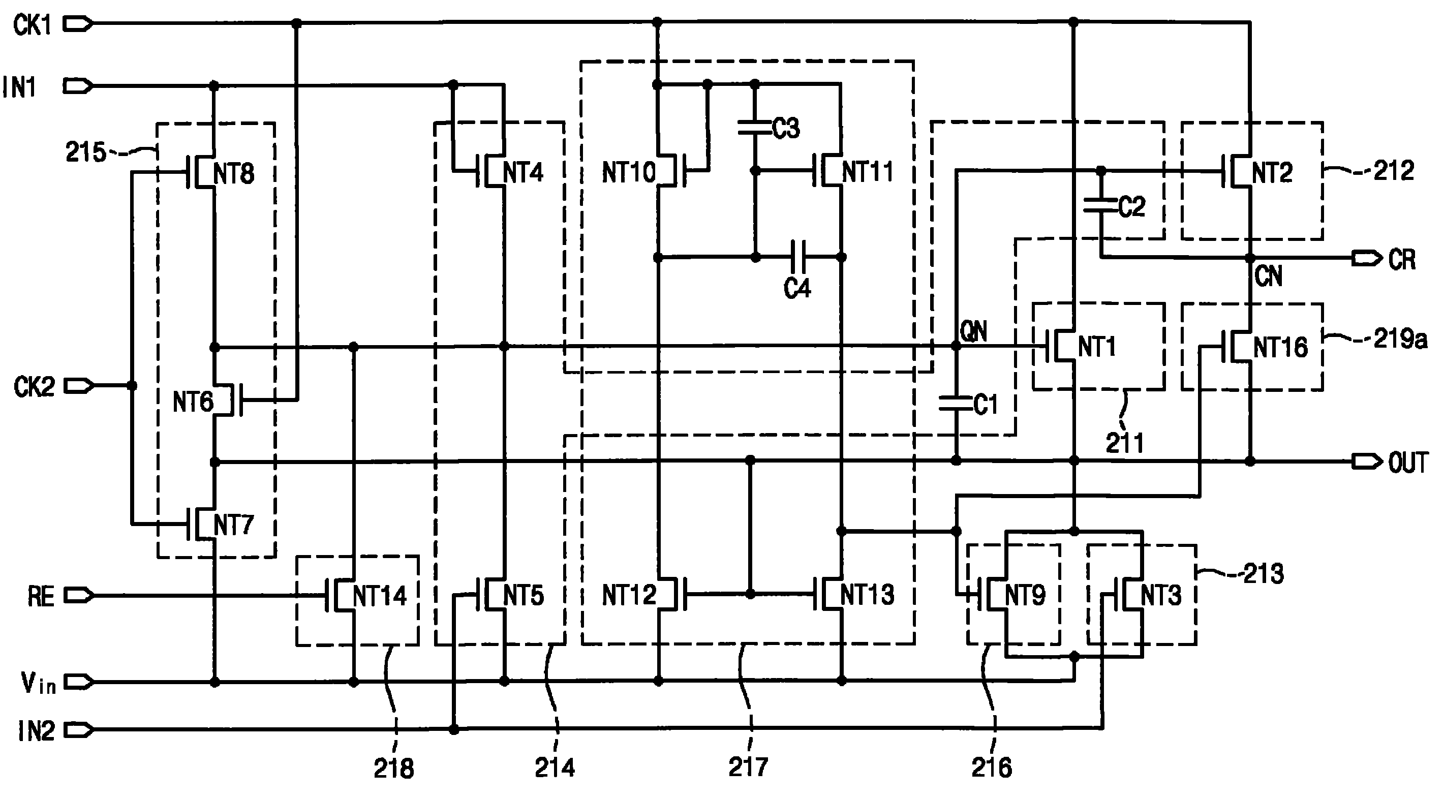
参照图3,每个级包括上拉部分211、负载部分212、下拉部分21 3、上拉驱动部分214、波纹防止部分215、保持部分216、反相器(inverter)217、复位部分218和第一浮置防止部分219a。Referring to FIG. 3, each stage includes a pull-up
上拉部分211包括上拉晶体管NT1,上拉晶体管NT1具有:控制电极,连接到上拉驱动部分214的输出端QN(Q节点QN);输入电极,连接到第一时钟端CK1;输出电极,连接到输出端OUT。因此,响应从上拉驱动部分214输出的控制电压,上拉晶体管NT1将通过输出端OUT输出的当前栅极电压上拉至通过第一时钟端CK1施加的时钟(下文中指图2中示出的第一时钟CKV)。上拉晶体管NT1仅在第一时间段内导通,所述第一时间段是在一帧内第一时钟CKV保持在高状态的一个水平扫描时间段(1H时间段),从而在第一时间段内保持当前栅极电压处于高状态。因此,在第一时间段内,当前栅极线导通。The pull-up
负载部分212包括负载晶体管NT2,负载晶体管NT2具有:控制电极,连接到Q节点QN;输入电极,连接到第一时钟端CK1;输出电极,连接到负载端CR。负载晶体管NT2响应从上拉驱动部分214输出的控制电压,将通过负载端CR输出的当前负载电压上拉至第一时钟CKV。负载晶体管NT2在一帧内只在第一时间段内导通,以在第一时间段内保持当前负载电压在高状态。The
下拉部分213包括下拉晶体管NT3,下拉晶体管NT3具有:控制电极,连接到第二输入端IN2;输入电极,连接到电压输出端Vin;输出电极,连接到输出端OUT。响应来自下一级的下一栅极电压,下拉晶体管NT3将当前栅极电压(即处于第一时钟CKV)下拉至通过电压输入端Vin提供的电源电压VSS(图2中所示)。即,下拉晶体管NT3在第一时间段后导通,从而将当前栅极电压下拉至低状态。The pull-down
上拉驱动部分214包括缓冲晶体管NT4、第一电容器C1、第二电容器C2和放电晶体管NT5。缓冲晶体管NT4包括共同连接到第一输入端IN1的输入电极和控制电极以及连接到Q节点QN的输出电极。第一电容器C1连接在Q节点QN和输出端OUT之间,第二电容器C2连接在负载晶体管NT2的控制电极和负载端CR之间。放电晶体管NT5包括:输入电极,连接到缓冲晶体管NT4的输出电极;控制电极,连接到第二输入端IN2;输出电极,连接到电压输入端Vin。The pull-up driving
当缓冲晶体管NT4响应来自前一级的前一负载电压而导通时,第一电容器C1和第二电容器C2充电。当比上拉晶体管NT1的阈值电压高的电压充入第一电容器C1时,Q节点QN的电势增大为高于阈值电压,使得上拉晶体管NT1和负载晶体管NT2导通。因此,通过输出端OUT和负载端CR来输出第一时钟CKV,从而将当前栅极电压和当前负载电压转变为高状态。因此,在第一时钟CKV的高时间段内,将当前栅极电压和当前负载电压保持在高状态。When the buffer transistor NT4 is turned on in response to the previous load voltage from the previous stage, the first capacitor C1 and the second capacitor C2 are charged. When a voltage higher than the threshold voltage of the pull-up transistor NT1 is charged into the first capacitor C1, the potential of the Q node QN increases to be higher than the threshold voltage, so that the pull-up transistor NT1 and the load transistor NT2 are turned on. Therefore, the first clock CKV is output through the output terminal OUT and the load terminal CR, thereby turning the current gate voltage and the current load voltage into a high state. Therefore, during the high period of the first clock CKV, the current gate voltage and the current load voltage are maintained in a high state.
然后,当响应来自下一级的下一栅极电压放电晶体管NT5导通时,充入第一电容器C1中的电荷通过放电晶体管NT5放电至电源电压VSS。因此,Q节点QN的电势降低至电源电压VSS,使得上拉晶体管NT1和负载晶体管NT2截止。即,由于放电晶体管NT5在第一时间段后导通以使上拉晶体管NT1和负载晶体管NT2截止,所以放电晶体管NT5可以防止通过输出端OUT和负载端CR输出的当前栅极电压和当前负载电压处于高状态。Then, when the discharge transistor NT5 is turned on in response to the next gate voltage from the next stage, the charge charged in the first capacitor C1 is discharged to the power supply voltage VSS through the discharge transistor NT5. Accordingly, the potential of the Q node QN is lowered to the power supply voltage VSS, so that the pull-up transistor NT1 and the load transistor NT2 are turned off. That is, since the discharge transistor NT5 is turned on to turn off the pull-up transistor NT1 and the load transistor NT2 after the first period of time, the discharge transistor NT5 can prevent the current gate voltage and the current load voltage output through the output terminal OUT and the load terminal CR is in a high state.
波纹防止部分215包括第一波纹防止晶体管NT6、第二波纹防止晶体管NT7和第三波纹防止晶体管NT8。波纹防止部分215可防止在一帧内的除了第一时间段之外的剩余的第二时间段(即,(n-1)H时间段)内,当前栅极电压和当前负载电压由于第一时钟CKV或第二时钟CKVB而产生波纹。The
第一波纹防止晶体管NT6包括:控制电极,连接到第一时钟端CK1;输入电极,连接到输出端OUT;输出电极,连接到Q节点QN。第二波纹防止晶体管NT7包括:控制电极,连接到第二时钟端CK2;输入电极,连接到输出端OUT;输出电极,连接到电压输入端Vin。第三波纹防止晶体管NT8包括:控制电极,连接到第二时钟端CK2;输入电极,连接到第一输入端IN1;输出电极,连接到Q节点QN。The first ripple prevention transistor NT6 includes: a control electrode connected to the first clock terminal CK1; an input electrode connected to the output terminal OUT; and an output electrode connected to the Q node QN. The second ripple prevention transistor NT7 includes: a control electrode connected to the second clock terminal CK2; an input electrode connected to the output terminal OUT; and an output electrode connected to the voltage input terminal Vin. The third ripple preventing transistor NT8 includes: a control electrode connected to the second clock terminal CK2; an input electrode connected to the first input terminal IN1; and an output electrode connected to the Q node QN.
在第二时间段内响应第一时钟CKV,第一波纹防止晶体管NT6向Q节点QN提供从输出端OUT输出的当前栅极电压(具有与截止电压相同的电压电平)。因此,在第二时间段内的第一时钟CKV的高时间段内,Q节点QN的电势保持在电源电压VSS。结果,第一波纹防止晶体管NT6防止上拉晶体管NT1和负载晶体管NT2在第二时间段内的第一时钟CKV的高时间段内导通。In response to the first clock CKV for the second period, the first ripple preventing transistor NT6 supplies the current gate voltage (having the same voltage level as the cut-off voltage) output from the output terminal OUT to the Q node QN. Therefore, during the high period of the first clock CKV within the second period, the potential of the Q node QN is maintained at the power supply voltage VSS. As a result, the first ripple preventing transistor NT6 prevents the pull-up transistor NT1 and the load transistor NT2 from being turned on during the high period of the first clock CKV within the second period.
第二波纹防止晶体管NT7响应第二时钟CKVB将当前栅极电压放电至电源电压VSS。因此,在第二时间段内的第二时钟CKVB的高时间段内,第二波纹防止晶体管NT7使当前栅极电压保持在电源电压VSS。The second ripple prevention transistor NT7 discharges the current gate voltage to the power supply voltage VSS in response to the second clock CKVB. Therefore, the second ripple preventing transistor NT7 maintains the current gate voltage at the power supply voltage VSS during the high period of the second clock CKVB within the second period.
响应通过第二时钟端CK2提供的时钟(下文中指图2中所示的第二时钟CKVB),第三波纹防止晶体管NT8向Q节点QN提供通过第一输入端IN1输入的来自前一级的前一负载电压(具有与电源电压VSS相同的电压电平)。因此,在第二时间段内在第二时钟CKVB的高时间段内,Q节点QN的电势保持在电源电压VSS。结果,第三波纹防止晶体管NT8防止上拉晶体管NT1和负载晶体管NT2在第二时间段内的第二时钟CKVB的高时间段内导通。In response to the clock supplied through the second clock terminal CK2 (hereinafter referred to as the second clock CKVB shown in FIG. 2 ), the third ripple preventing transistor NT8 supplies the Q node QN with the previous clock from the previous stage input through the first input terminal IN1. A load voltage (having the same voltage level as the power supply voltage VSS). Therefore, the potential of the Q node QN is maintained at the power supply voltage VSS during the high period of the second clock CKVB during the second period. As a result, the third ripple preventing transistor NT8 prevents the pull-up transistor NT1 and the load transistor NT2 from being turned on during the high period of the second clock CKVB within the second period.
下面将用第一浮置防止部分219a来描述使前一负载电压保持在与电源电压VSS的电压电平相同的电压电平的过程。The process of maintaining the previous load voltage at the same voltage level as that of the power supply voltage VSS will be described below using the first floating preventing
保持部分216包括保持晶体管NT9,保持晶体管NT9具有:控制电极,连接到反相器217的输出端;输入电极,连接到电压输入端Vin;输出电极,连接到输出端OUT。The holding
反相器217包括第一反相器晶体管NT10、第二反相器晶体管NT11、第三反相器晶体管NT12、第四反相器晶体管NT13、第三电容器C3和第四电容器C4,以使保持晶体管NT9导通和截止。The
第一反相器晶体管NT10包括:输入电极和控制电极,共同连接到第一时钟端CK1;输出电极,通过第四电容器C4连接到第二反相器晶体管NT11的输出电极。第二反相器晶体管NT11包括:输入电极,连接到第一时钟端CK1;控制电极,通过第三电容器C3连接到其输入电极;输出电极,连接到保持晶体管NT9的控制电极。第三反相器晶体管NT12包括:输入电极,连接到第一反相器晶体管NT10的输出电极;控制电极,连接到输出端OUT;输出电极,连接到电压输入端Vin。第四反相器晶体管NT13包括:输入电极,连接到保持晶体管NT9的控制电极;控制电极,连接到输出端OUT;输出电极,连接到电压输入端Vin。The first inverter transistor NT10 includes: an input electrode and a control electrode commonly connected to the first clock terminal CK1; an output electrode connected to the output electrode of the second inverter transistor NT11 through the fourth capacitor C4. The second inverter transistor NT11 includes: an input electrode connected to the first clock terminal CK1; a control electrode connected to its input electrode through the third capacitor C3; and an output electrode connected to the control electrode of the holding transistor NT9. The third inverter transistor NT12 includes: an input electrode connected to the output electrode of the first inverter transistor NT10; a control electrode connected to the output terminal OUT; and an output electrode connected to the voltage input terminal Vin. The fourth inverter transistor NT13 includes: an input electrode connected to the control electrode of the holding transistor NT9; a control electrode connected to the output terminal OUT; and an output electrode connected to the voltage input terminal Vin.
第三反相器晶体管NT12和第四反相器晶体管NT13响应保持在高状态并输出到输出端OUT的当前栅极电压而导通,从第一反相器晶体管NT10和第二反相器晶体管NT11输出的第一时钟CKV放电至电源电压VSS。因此,在当前栅极电压保持在高状态的第一时间段内,保持晶体管NT9截止。在当前栅极电压转变为低状态时,第三反相器晶体管NT12和第四反相器晶体管NT13截止。因此,响应从第一反相器晶体管NT10和第二反相器晶体管NT11输出的第一时钟CKV,保持晶体管NT9导通。结果,保持晶体管NT9保持当前栅极电压在第二时间段内的第一时钟CKV的高时间段内处于电源电压VSS的电平。The third inverter transistor NT12 and the fourth inverter transistor NT13 are turned on in response to the current gate voltage held in the high state and output to the output terminal OUT, from the first inverter transistor NT10 and the second inverter transistor The first clock CKV output by NT11 is discharged to the power supply voltage VSS. Therefore, during the first period of time when the current gate voltage is kept in the high state, the transistor NT9 is kept turned off. When the current gate voltage transitions to a low state, the third and fourth inverter transistors NT12 and NT13 are turned off. Accordingly, the transistor NT9 is kept turned on in response to the first clock CKV output from the first inverter transistor NT10 and the second inverter transistor NT11. As a result, the sustain transistor NT9 maintains the current gate voltage at the level of the power supply voltage VSS during the high period of the first clock CKV within the second period.
复位部分218包括复位晶体管NT14,复位晶体管NT14具有:控制电极,连接到复位端RE;输入电极,连接到上拉晶体管NT1的控制电极;输出电极,连接到电压输入端Vin。响应通过复位端RE输入的最后一级SRCn+1的最后一个负载电压(图2中所示),复位晶体管NT14将通过第一输入端IN1输入的噪声放电至电源电压VSS。因此,上拉晶体管NT1和负载晶体管NT2响应来自最后一级SRCn+1的最后一个负载电压而截止。结果,最后一个负载电压被提供到所有n级的复位端RE,以使每个级的上拉晶体管NT1和负载晶体管NT2截止,从而将所有级复位。The
第一浮置防止部分219a包括第一浮置防止晶体管NT16,第一浮置防止晶体管NT16具有:控制电极,连接到反相器217的输出端;输入电极,连接到输出端OUT;输出电极,连接到当前负载节点CN。第一浮置防止晶体管NT16响应反相器217的输出信号而导通或截止。具体地讲,第一浮置防止晶体管NT16响应反相器217的低输出信号在第一时间段内截止。然后,第一浮置防止晶体管NT16响应反相器217的高输出信号在第二时间段内的第一时钟CKV的高时间段内导通。导通的第一浮置防止晶体管NT1 6向当前负载节点CN输出在第二时间段内保持在低状态的当前栅极电压。因此,第一浮置防止晶体管NT16在第二时间段内的第一时钟CKV的高时间段内将当前负载节点CN复位到电源电压VSS。The first
如图2所示,当前负载节点CN(即负载端CR)连接到下一级的第一输入端IN1。因此,在第二时间段内的第一时钟CKV的高时间段内,与电源电压VSS具有相同电压电平的负载电压被施加到下一级的第一输入端IN1。结果,在第二时间段内的第一时钟CKV的高时间段内,下一级的Q节点的电势可以保持在电源电压VSS。因此,当前级的第一浮置防止晶体管NT16可以防止下一级的Q节点浮置。As shown in FIG. 2 , the current load node CN (that is, the load terminal CR) is connected to the first input terminal IN1 of the next stage. Therefore, during the high period of the first clock CKV within the second period, the load voltage having the same voltage level as the power supply voltage VSS is applied to the first input terminal IN1 of the next stage. As a result, the potential of the Q node of the next stage can be maintained at the power supply voltage VSS during the high period of the first clock CKV within the second period. Therefore, the first floating preventing transistor NT16 of the current stage can prevent the Q node of the next stage from floating.
图4是示出了在第二时间段内的第一时钟CKV的高时间段内Q节点的电势的电路图,图5是示出了在第二时间段内的第二时钟CKVB的高时间段内Q节点的电势的电路图。在图4和图5中,将部分示出移位寄存器的每个级中的第i级(i是大于1小于n的奇数)的电路。4 is a circuit diagram showing the potential of the Q node in the high period of the first clock CKV in the second period, and FIG. 5 is a circuit diagram showing the high period of the second clock CKVB in the second period. Circuit diagram of the potential within the Q node. In FIGS. 4 and 5 , the circuit of the i-th stage (i is an odd number greater than 1 and smaller than n) in each stage of the shift register will be partially shown.
参照图4,为了在第i栅极电压Gi保持在低状态(例如电源电压VSS的电平)的第二时间段内的第一时钟CKV的高时间段内将Q节点QN的电势保持在电源电压VSS,保持晶体管NT9和第一波纹防止晶体管NT6导通。Referring to FIG. 4, in order to maintain the potential of the Q node QN at the power supply during the high period of the first clock CKV within the second period during which the i-th gate voltage Gi remains in a low state (for example, the level of the power supply voltage VSS) Voltage VSS, keeps transistor NT9 and first ripple preventing transistor NT6 from turning on.
具体地讲,反相器217响应第一时钟CKV来输出高输出信号,以导通保持晶体管NT9,从而输出电源电压VSS。由于之前第一波纹防止晶体管NT6响应第一时钟CKV而导通,所以从保持晶体管NT9输出的电源电压VSS通过第一波纹防止晶体管NT6施加到Q节点QN。因此,Q节点QN的电势保持在电源电压VSS,连接到Q节点QN的上拉晶体管NT1和负载晶体管NT2截止。因此,可以防止第i栅极电压Gi和第i负载电压Ci在第二时间段内的第一时钟CKV的高时间段内产生波纹。Specifically, the
从保持晶体管NT9输出的电源电压VSS还输出到第i级SRCi的输出端OUT,使得第i栅极电压Gi保持在电源电压VSS。The power supply voltage VSS output from the holding transistor NT9 is also output to the output terminal OUT of the i-th stage SRCi, so that the i-th gate voltage Gi is maintained at the power supply voltage VSS.
第一浮置防止晶体管NT16响应来自反相器217的高输出信号而导通,从而将第i级SRCi的负载节点CN的电势保持在电源电压VSS。具有电源电压VSS的电平的第i负载电压Ci从第i级SRCi输出并被施加到第i+1级(未示出)的第一输入端IN1。The first floating prevention transistor NT16 is turned on in response to the high output signal from the
参照图5,为了在第i栅极电压Gi保持在低状态(例如电源电压VSS的电平)的第二时间段内的第二时钟CKVB的高时间段内将Q节点QN的电势保持在电源电压VSS,第三波纹防止晶体管NT8导通。Referring to FIG. 5, in order to maintain the potential of the Q node QN at the power supply during the high period of the second clock CKVB within the second period during which the i-th gate voltage Gi remains in a low state (for example, the level of the power supply voltage VSS) Voltage VSS, the third ripple prevents transistor NT8 from turning on.
第i级SRCi的第三波纹防止晶体管NT8的输入电极连接到第i-1级SRCi-1的负载节点CN,因为第i-1栅极电压Gi-1具有电源电压VSS的电平,所以通过第i-1级SRCi-1的第一浮置防止晶体管NT16,第i-1级SRCi-1的负载节点CN保持在电源电压VSS。因此,具有电源电压VSS的电平的第i-1负载电压Ci-1被施加到第i级SRCi的第三波纹防止晶体管NT8的输入电极。第i-1负载电压Ci-1通过第三波纹防止晶体管NT8被施加到第i级SRCi的Q节点QN。The input electrode of the third ripple preventing transistor NT8 of the i-th stage SRCi is connected to the load node CN of the i-1-th stage SRCi-1, and since the i-1-th gate voltage Gi-1 has the level of the power supply voltage VSS, it passes The first floating prevention transistor NT16 of the i-1th stage SRCi-1, and the load node CN of the i-1th stage SRCi-1 are maintained at the power supply voltage VSS. Accordingly, the i-1th load voltage Ci-1 having the level of the power supply voltage VSS is applied to the input electrode of the third ripple preventing transistor NT8 of the i-th stage SRCi. The i-1th load voltage Ci-1 is applied to the Q node QN of the i-th stage SRCi through the third ripple preventing transistor NT8.
因此,第i级SRCi中的Q节点QN的电势保持在电源电压VSS的电平,连接到Q节点QN的上拉晶体管NT1和负载晶体管NT2截止。因此,可以在第二时间段内的第二时钟CKVB的高时间段内防止第i负载电压Ci和第i栅极电压Gi的波纹。Therefore, the potential of the Q node QN in the i-th stage SRCi is kept at the level of the power supply voltage VSS, and the pull-up transistor NT1 and the load transistor NT2 connected to the Q node QN are turned off. Accordingly, ripples in the i-th load voltage Ci and the i-th gate voltage Gi may be prevented during the high time period of the second clock CKVB in the second time period.
图6是示出了根据本发明另一示例性实施例的栅极驱动电路的每个级的电路图。在图6中,相同的标号表示与图3中的元件相同的元件,因此将省略对相同元件的详细描述。FIG. 6 is a circuit diagram illustrating each stage of a gate driving circuit according to another exemplary embodiment of the present invention. In FIG. 6 , the same reference numerals denote the same elements as those in FIG. 3 , and thus detailed descriptions of the same elements will be omitted.
参照图6,每个级包括上拉部分211、负载部分212、下拉部分213、上拉驱动部分214、波纹防止部分215、保持部分216、反相器217、复位部分218、第一浮置防止部分219a和第二浮置防止部分219b。6, each stage includes a pull-up
第二浮置防止部分219b包括第二浮置防止晶体管NT17,第二浮置防止晶体管NT17具有:控制电极,连接到第一时钟端CK1;输入电极,连接到电压输入端Vin;输出电极,连接到第一输入端IN1。The second
在当前栅极电压保持在低状态的第二时间段内的输入到第一时钟端CK1的第一时钟CKV(图2中示出)的高时间段内,第二浮置防止晶体管NT17响应第一时钟CKV而导通。因此,第二浮置防止晶体管NT17将施加到电压输入端Vin的电源电压VSS提供到第一输入端IN1。在本示例性实施例中,第一输入端IN1连接到前一级的负载节点CN(即负载端CR)。During the high time period of the first clock CKV (shown in FIG. 2 ) input to the first clock terminal CK1 during the second time period in which the current gate voltage remains in the low state, the second floating prevention transistor NT17 responds to the first A clock CKV is turned on. Accordingly, the second floating prevention transistor NT17 supplies the power supply voltage VSS applied to the voltage input terminal Vin to the first input terminal IN1. In this exemplary embodiment, the first input terminal IN1 is connected to the load node CN (ie, the load terminal CR) of the previous stage.
因此,在第二时间段内的第一时钟CKV的高时间段内,第二浮置防止晶体管NT17向前一级的负载节点CN施加电源电压VSS,以使负载节点CN复位。因此,第二浮置防止晶体管NT17防止前一负载节点CN浮置。Therefore, during the high period of the first clock CKV within the second period, the second floating prevention transistor NT17 applies the power supply voltage VSS to the load node CN of the previous stage to reset the load node CN. Therefore, the second floating prevention transistor NT17 prevents the previous load node CN from floating.
图7是示出了根据本发明另一示例性实施例的栅极驱动电路的每个级的电路图。在图7中,相同的标号表示与图6中的元件相同的元件,因此,将省略对相同元件的详细描述。FIG. 7 is a circuit diagram illustrating each stage of a gate driving circuit according to another exemplary embodiment of the present invention. In FIG. 7, the same reference numerals denote the same elements as those in FIG. 6, and thus, detailed descriptions of the same elements will be omitted.
参照图7,每个级包括上拉部分211、负载部分212、下拉部分213、上拉驱动部分214、波纹防止部分215、保持部分216、反相器217、复位部分218、第二浮置防止部分219b和第三浮置防止部分219c。7, each stage includes a pull-up
第三浮置防止部分219c包括第三浮置防止晶体管NT18,第三浮置防止晶体管NT18具有:控制电极,连接到反相器217的输出端;输入电极,连接到电压输入端Vin;输出电极,连接到当前负载节点CN。第三浮置防止晶体管响应反相器217的输出信号而导通或截止。The third floating preventing part 219c includes a third floating preventing transistor NT18 having: a control electrode connected to the output terminal of the
具体地讲,在一帧内的第一时间段内,第三浮置防止晶体管NT18响应反相器217的低输出信号而截止。然而,在一帧中除了第一时间段外的第二时间段内的第一时钟CKV的高时间段内,第三浮置防止晶体管NT18响应反相器217的高输出信号而导通。导通的第三浮置防止晶体管NT18将输入到电压输入端Vin的电源电压VSS(图2中示出)输出至当前负载节点CN。因此,在第二时间段内的第一时钟CKV的高时间段内,第三浮置防止晶体管NT18将当前负载节点CN的电势复位至电源电压VSS的电平。Specifically, the third floating prevention transistor NT18 is turned off in response to the low output signal of the
图8是示出了根据本发明另一示例性实施例的栅极驱动电路的框图。在图8中,相同的标号表示与图2中的元件相同的元件,因此将省略对相同元件的详细描述。FIG. 8 is a block diagram illustrating a gate driving circuit according to another exemplary embodiment of the present invention. In FIG. 8 , the same reference numerals denote the same elements as those in FIG. 2 , and thus detailed descriptions of the same elements will be omitted.
参照图8,栅极驱动电路210包括移位寄存器210a,移位寄存器210a具有彼此串联连接的多个级SRC1-SRCn+1。移位寄存器210a布置成与栅极线GL1-GLn的第一端相邻。每个级包括第一输入端IN1、第一时钟端CK1、第二时钟端CK2、第二输入端IN2、第一电压输入端Vin-1、复位端RE、第二电压输入端Vin-2、输出端OUT和负载端CR。Referring to FIG. 8, the gate driving circuit 210 includes a
第一电源电压VSS1被提供到级SRC1-SRCn+1的第一电压输入端Vin-1。第一电源电压VSS1可以是地电平电压或负电压。比第一电源电压VSS1低的第二电源电压VSS2被施加到第二电压输入端Vin-2。在本示例性实施例中,第一电源电压VSS1是大约-6.7V,第二电源电压VSS2是大约-13V。The first supply voltage VSS1 is supplied to the first voltage input Vin-1 of the stages SRC1-
图9是示出图8中的每个级的电路图。在图8中,由于栅极驱动电路的每个级具有相同的结构,所以将参照图9仅详细描述一级,而为了避免冗长将省略对其它级的详细描述。FIG. 9 is a circuit diagram showing each stage in FIG. 8 . In FIG. 8 , since each stage of the gate driving circuit has the same structure, only one stage will be described in detail with reference to FIG. 9 , and detailed descriptions of other stages will be omitted to avoid redundancy.
参照图9,每个级包括上拉部分211、负载部分212、下拉部分213、上拉驱动部分214、波纹防止部分215a、保持部分216、反相器217、复位部分218和第四浮置防止部分219d。9, each stage includes a pull-up
下拉部分213包括下拉晶体管NT3,下拉晶体管NT3具有:控制电极,连接到第二输入端IN2;输入电极,连接到第一电压输入端Vin-1;输出电极,连接到输出端OUT。响应来自下一级的下一栅极电压,下拉晶体管NT3将当前栅极电压(处于第一时钟CKV)下拉至通过第-电压输入端Vin-1提供的第一电源电压VSS1(图8中示出)。即,在一帧内的第一时间段内产生处于高状态的当前栅极电压,而下拉晶体管NT3在第一时间段(1H时间段)之后导通,以将当前栅极电压下拉至低状态。The pull-down
上拉驱动部分214包括缓冲晶体管NT4、第一电容器C1、第二电容器C2和放电晶体管NT5。放电晶体管NT5包括:输入电极,连接到缓冲晶体管NT4的输出电极;控制电极,连接到第二输入端IN2;输出电极,连接到第一电压输入端Vin-1。The pull-up driving
当放电晶体管NT5响应来自下一级的下一栅极电压而导通时,充入到第一电容器C1中的电荷通过放电晶体管NT5放电至第一电源电压VSS1。因此,将Q节点QN的电势降低至第一电源电压VSS1,使得上拉晶体管NT1和负载晶体管NT2截止。When the discharge transistor NT5 is turned on in response to the next gate voltage from the next stage, the charge charged in the first capacitor C1 is discharged to the first power supply voltage VSS1 through the discharge transistor NT5. Accordingly, the potential of the Q node QN is lowered to the first power supply voltage VSS1, so that the pull-up transistor NT1 and the load transistor NT2 are turned off.
波纹防止部分215a包括第一波纹防止晶体管NT6、第二波纹防止晶体管NT7、第三波纹防止晶体管NT8。波纹防止部分215a防止当前栅极电压和当前负载电压在一帧内的除了第一时间段之外的剩余的第二时间段(即,(n-1)H时间段)内由于第一时钟CKV或第二时钟CKVB而产生波纹。The
第一波纹防止晶体管NT6包括:控制电极,连接到第一时钟端CK1;输入电极,连接到输出端OUT;输出电极,连接到Q节点QN。第二波纹防止晶体管NT7包括:控制电极,连接到第二时钟端CK2;输入电极,连接到输出端OUT;输出电极,连接到第一电压输入端Vin-1。第三波纹防止晶体管NT8包括:控制电极,连接到第二时钟端CK2;输入电极,连接到第一输入端IN1;输出电极,连接到Q节点QN。The first ripple prevention transistor NT6 includes: a control electrode connected to the first clock terminal CK1; an input electrode connected to the output terminal OUT; and an output electrode connected to the Q node QN. The second ripple preventing transistor NT7 includes: a control electrode connected to the second clock terminal CK2; an input electrode connected to the output terminal OUT; an output electrode connected to the first voltage input terminal Vin-1. The third ripple preventing transistor NT8 includes: a control electrode connected to the second clock terminal CK2; an input electrode connected to the first input terminal IN1; and an output electrode connected to the Q node QN.
保持部分216包括保持晶体管NT9,保持晶体管NT9具有:控制电极,连接到反相器217的输出端;输入电极,连接到第一电压输入端Vin-1;输出电极,连接到输出端OUT。The holding
反相器217包括第一反相器晶体管NT10、第二反相器晶体管NT11、第三反相器晶体管NT12、第四反相器晶体管NT13、第三电容器C3、第四电容器C4,以使保持晶体管NT9导通或截止。The
第一反相器晶体管NT10包括:输入电极和控制电极,共同连接到第一时钟端CK1;输出电极,通过第四电容器C4连接到第二反相器晶体管NT11的输出电极。第二反相器晶体管NT11包括:输入电极,连接到第一时钟端CK1;控制电极,通过第三电容器C3连接到其输入电极;输出电极,连接到保持晶体管NT9的控制电极。第三反相器晶体管NT12包括:输入电极,连接到第一反相器晶体管NT10的输出电极;控制电极,连接到输出端OUT;输出电极,连接到第一电压输入端Vin-1。第四反相器晶体管NT13包括:输入电极,连接到保持晶体管NT9的控制电极;控制电极,连接到输出端OUT;输出电极,连接到第一电压输入端Vin-1。The first inverter transistor NT10 includes: an input electrode and a control electrode commonly connected to the first clock terminal CK1; an output electrode connected to the output electrode of the second inverter transistor NT11 through the fourth capacitor C4. The second inverter transistor NT11 includes: an input electrode connected to the first clock terminal CK1; a control electrode connected to its input electrode through the third capacitor C3; and an output electrode connected to the control electrode of the holding transistor NT9. The third inverter transistor NT12 includes: an input electrode connected to the output electrode of the first inverter transistor NT10; a control electrode connected to the output terminal OUT; and an output electrode connected to the first voltage input terminal Vin-1. The fourth inverter transistor NT13 includes: an input electrode connected to the control electrode of the holding transistor NT9; a control electrode connected to the output terminal OUT; and an output electrode connected to the first voltage input terminal Vin-1.
第三反相器晶体管NT12和第四反相器晶体管NT13响应高状态的当前栅极电压而导通,从第一反相器晶体管NT10和第二反相器晶体管NT11输出的第一时钟CKV放电至第一电源电压VSS1。因此,在当前栅极电压保持在高状态的第一时间段内,保持晶体管NT9截止。在当前栅极电压转变成低状态时,第三反相器晶体管NT12和第四反相器晶体管NT13截止。因此,保持晶体管NT9响应从第一反相器晶体管NT10和第二反相器晶体管NT11输出的第一时钟CKV而导通。因此,保持晶体管NT9可以在第二时间段内的第一时钟CKV的高时间段内将当前栅极电压保持在第一电源电压VSS1。The third inverter transistor NT12 and the fourth inverter transistor NT13 are turned on in response to the current gate voltage of the high state, and the first clock CKV output from the first inverter transistor NT10 and the second inverter transistor NT11 is discharged to the first supply voltage VSS1. Therefore, during the first period of time when the current gate voltage is kept in the high state, the transistor NT9 is kept turned off. When the current gate voltage transitions to a low state, the third and fourth inverter transistors NT12 and NT13 are turned off. Accordingly, the sustain transistor NT9 is turned on in response to the first clock CKV output from the first and second inverter transistors NT10 and NT11. Therefore, the sustain transistor NT9 may maintain the current gate voltage at the first power supply voltage VSS1 during the high period of the first clock CKV within the second period.
复位部分218包括复位晶体管NT14,复位晶体管NT14具有:控制电极,连接到复位端RE;输入电极,连接到上拉晶体管NT1的控制电极;输出电极,连接到第一电压输入端Vin-1。响应通过复位端RE输入的来自最后一级SRCn+1(图8中示出)的最后一个负载电压,复位晶体管NT14将通过第一输入端IN1输入的噪声放电至第一电源电压VSS1。The
第四浮置防止部分219d包括第四浮置防止晶体管NT19,第四浮置防止晶体管NT19具有:控制电极,连接到反相器217的输出端;输入电极,连接到第二电压输入端Vin-2;输出电极,连接到当前负载节点CN。第四浮置防止晶体管NT19响应反相器217的输出信号而导通或截止。具体地讲,第四浮置防止晶体管NT19在第一时间段内响应反相器217的低输出信号而截止。然后,在第二时间段内的第一时钟CKV的高时间段内,第四浮置防止晶体管NT19响应反相器217的高输出信号而导通。导通的第四浮置防止晶体管NT19将通过第二电压输入端Vin-2施加的第二电源电压VSS2输出至当前负载节点CN。因此,在第二时间段内的第一时钟CKV的高时间段内,第四浮置防止晶体管NT19将当前负载节点CN的电势复位至第二电源电压VSS2的电平。The fourth
如图8中所示,当前负载节点CN连接到下一级的第一输入端IN1。因此,在第二时间段内的第一时钟CKV的高时间段内,电压电平与第二电源电压VSS2的电平相同的负载电压被施加到下一级的第一输入端IN1。因此,在第二时间段内的第一时钟CKV的高时间段内,下一级的Q节点QN的电势可以保持在第二电源电压VSS2的电平。因此,当前级的第四浮置防止晶体管NT19可以防止下一级的Q节点QN浮置。As shown in FIG. 8, the current load node CN is connected to the first input terminal IN1 of the next stage. Therefore, during the high time period of the first clock CKV in the second time period, the load voltage having the same voltage level as that of the second power supply voltage VSS2 is applied to the first input terminal IN1 of the next stage. Therefore, during the high period of the first clock CKV within the second period, the potential of the Q node QN of the next stage can be maintained at the level of the second power supply voltage VSS2. Therefore, the fourth floating prevention transistor NT19 of the current stage can prevent the Q node QN of the next stage from floating.
图10是示出在第二时间段内的第一时钟CKV的高时间段内的Q节点的电势的电路图,图11是示出在第二时间段内的第二时钟CKVB的高时间段内的Q节点的电势的电路图。在图10和图11中,将部分示出移位寄存器的各级之中的第i级(i是大于1小于n的奇数)的电路。10 is a circuit diagram showing the potential of the Q node in the high period of the first clock CKV in the second period, and FIG. 11 is a circuit diagram showing the potential in the high period of the second clock CKVB in the second period. Circuit diagram of the potential of the Q node. In FIGS. 10 and 11 , the circuit of the i-th stage (i is an odd number greater than 1 and smaller than n) among the stages of the shift register will be partially shown.
参照图10,在第i栅极电压Gi保持在低状态(即第一电源电压VSS1的电平)的第二时间段内的第一时钟CKV的高时间段内,保持晶体管NT9和第一波纹防止晶体管NT6导通,以使Q节点QN的电势保持在第一电压电源VSS1的电平。Referring to FIG. 10, during the high time period of the first clock CKV during the second time period in which the i-th gate voltage Gi remains in a low state (that is, the level of the first power supply voltage VSS1), the transistor NT9 and the first ripple The transistor NT6 is prevented from being turned on so that the potential of the Q node QN is kept at the level of the first voltage supply VSS1.
具体地讲,反相器217响应第一时钟CKV输出高输出信号,以导通保持晶体管NT9,从而输出第一电源电压VSS1。由于之前第一波纹防止晶体管NT6响应第一时钟CKV导通,所以从保持晶体管NT9输出的第一电源电压VSS1通过第一波纹防止晶体管NT6被施加到Q节点QN。因此,Q节点QN的电势保持在第一电源电压VSS1的电平,连接到Q节点QN的上拉晶体管NT1和负载晶体管NT2截止。结果,可以防止在第二时间段内的第一时钟CKV的高时间段内第i栅电极Gi和第i负载电压Ci产生波纹。Specifically, the
从保持晶体管NT9输出的第一电源电压VSS1还输出到第i级SRCi的输出端OUT,使得第i栅极电压Gi保持在第一电源电压VSS1的电平。The first power supply voltage VSS1 output from the sustain transistor NT9 is also output to the output terminal OUT of the i-th stage SRCi, so that the i-th gate voltage Gi is maintained at the level of the first power supply voltage VSS1.
由于第四浮置防止晶体管NT19响应来自反相器217的高输出信号而导通,所以第i级SRCi的负载节点CN的电势保持在第二电源电压VSS2的电平。具有第二电源电压VSS2的电平的第i负载电压Ci从第i级SRCi输出,并被施加到第i+1级(未示出)的第一输入端IN1。Since the fourth floating prevention transistor NT19 is turned on in response to the high output signal from the
参照图11,在第i栅极电压Gi保持在低状态(即,第一电源电压VSS1的电平)的第二时间段内的第二时钟CKVB的高时间段内,第三波纹防止晶体管NT8导通,以使Q节点QN的电势保持在第二电源电压VSS2的电平。Referring to FIG. 11, during the high time period of the second clock CKVB during the second time period in which the i-th gate voltage Gi remains in the low state (ie, the level of the first power supply voltage VSS1), the third ripple prevention transistor NT8 turned on to keep the potential of the Q node QN at the level of the second power supply voltage VSS2.
第i级SRCi的第三波纹防止晶体管NT8的输入电极连接到第i-1级SRCi-1的负载节点CN,通过第i-1级SRCi-1的第四浮置防止晶体管NT19,第i-1级SRCi-1的负载节点CN保持在第二电源电压VSS2的电平。因此,具有第二电源电压VSS2的电平的第i-1负载电压Ci-1被施加到第i级SRCi的第三波纹防止晶体管NT8的输入电极。第i-1负载电压Ci-1通过第三波纹防止晶体管NT8被施加到第i级SRCi的Q节点QN。The input electrode of the third ripple prevention transistor NT8 of the i-th stage SRCi is connected to the load node CN of the i-1-th stage SRCi-1, and through the fourth floating prevention transistor NT19 of the i-1-th stage SRCi-1, the i-th The load node CN of the
因此,第i级SRCi的Q节点QN的电势保持在第二电源电压VSS2的电平,连接到Q节点QN的上拉晶体管NT1和负载晶体管NT2截止。因此,可以防止在第二时间段内的第二时钟CKVB的高时间段内第i栅极电压Gi和第i负载电压Ci产生波纹。Therefore, the potential of the Q node QN of the i-th stage SRCi is maintained at the level of the second power supply voltage VSS2, and the pull-up transistor NT1 and the load transistor NT2 connected to the Q node QN are turned off. Therefore, it is possible to prevent the i-th gate voltage Gi and the i-th load voltage Ci from being rippled during the high time period of the second clock CKVB in the second time period.
图12是示出了Q节点QN的电势作为时间的函数的曲线图。在图12中,第一曲线G1表示在级不包括第四浮置防止晶体管NT19的情况下Q节点QN的电势,第二曲线G2表示在当前栅极信号被施加到第四浮置防止晶体管NT19的情况下Q节点QN的电势,第三曲线G3表示在第二电源电压VSS2被施加到第四浮置防止晶体管NT19的情况下Q节点QN的电势,第四曲线G4表示当前栅极电压。FIG. 12 is a graph showing the potential of the Q node QN as a function of time. In FIG. 12, the first graph G1 represents the potential of the Q node QN in the case where the stage does not include the fourth floating preventing transistor NT19, and the second graph G2 represents the potential of the Q node QN when the current gate signal is applied to the fourth floating preventing transistor NT19. The third graph G3 represents the potential of the Q node QN in the case where the second power supply voltage VSS2 is applied to the fourth floating prevention transistor NT19, and the fourth graph G4 represents the current gate voltage.
参照图12,根据第一曲线G1和第四曲线G4,在Q节点QN(图10和图11中示出)的电势提升的第一时间段A1内,当前栅极电压保持在导通状态。然后,当前栅极电压在第二时间段A2内保持截止状态。Referring to FIG. 12 , according to the first graph G1 and the fourth graph G4 , the current gate voltage is maintained in the on state during the first period A1 of the potential rise of the Q node QN (shown in FIGS. 10 and 11 ). Then, the current gate voltage remains in the off state for the second time period A2.
在如第一曲线G1表示的级不包括第四浮置防止晶体管NT19的情况下,在高温条件下,在第一时钟CKV(图10中示出)的高时间段B1和B3和第二时钟CKVB(图11中示出)的高时间段B2和B4内,在Q节点QN出现波纹。具体地讲,当在级中不包括第四浮置防止晶体管NT19时,在第二时钟CKVB的高时间段B2和B4内,前一负载节点CN浮置。因此,在第二时钟CKVB的高时间段B2和B4内,Q节点QN的电势不稳定。In the case that the stage represented by the first curve G1 does not include the fourth floating prevention transistor NT19, under high temperature conditions, during the high periods B1 and B3 of the first clock CKV (shown in FIG. 10 ) and the second clock Ripple occurs at Q node QN during high periods B2 and B4 of CKVB (shown in FIG. 11 ). Specifically, when the fourth floating prevention transistor NT19 is not included in the stage, the previous load node CN floats during the high periods B2 and B4 of the second clock CKVB. Therefore, the potential of the Q node QN is unstable during the high periods B2 and B4 of the second clock CKVB.
然而,在如第二曲线G2表示的当前栅极信号被施加到第四浮置防止晶体管NT19的情况下,在高温条件下在第二时钟CKVB的高时间段B2和B4内的Q节点QN的波纹的大小变得小于在级中不包括第四浮置防止晶体管NT19的情况下的波纹的大小。具体地讲,在高温条件下在第二时钟CKVB的高时间段B2和B4内,通过第四浮置防止晶体管NT19将降低至大约-6.7V的第一电源电压VSS1的当前栅极信号施加到前一负载节点CN。因此,可以减小Q节点QN的波纹的大小。However, in the case where the current gate signal as represented by the second graph G2 is applied to the fourth floating prevention transistor NT19, the Q node QN during the high periods B2 and B4 of the second clock CKVB under high temperature conditions The size of the ripple becomes smaller than that of the case where the fourth floating prevention transistor NT19 is not included in the stage. Specifically, during the high periods B2 and B4 of the second clock CKVB under high temperature conditions, the current gate signal of the first power supply voltage VSS1 lowered to about -6.7V is applied to the The previous load node CN. Therefore, the size of the ripple of the Q node QN can be reduced.
在如第三曲线G3示出的大约-13V的第二电源电压VSS2被施加到第四浮置防止晶体管NT19的情况下,在高温条件下在第二时钟CKVB的高时间段B2和B4内的Q节点QN的波纹的大小变得小于前两种情况下的波纹的大小。即,在第二时钟CKVB的高时间段B2和B4内,通过第四浮置防止晶体管NT19将低于第一电源电压VSS1的第二电源电压VSS2施加到前一负载节点CN。因此,Q节点QN的电势变得更稳定,从而减小了Q节点QN的波纹的大小。In the case where the second power supply voltage VSS2 of about -13V is applied to the fourth floating preventing transistor NT19 as shown in the third graph G3, the high periods B2 and B4 of the second clock CKVB are under high temperature conditions. The size of the ripple of the Q node QN becomes smaller than that of the previous two cases. That is, during the high periods B2 and B4 of the second clock CKVB, the second power supply voltage VSS2 lower than the first power supply voltage VSS1 is applied to the previous load node CN through the fourth floating preventing transistor NT19. Therefore, the potential of the Q node QN becomes more stable, thereby reducing the size of the ripple of the Q node QN.
图13是根据本发明另一示例性实施例的栅极驱动电路的级的电路图。在图13中,相同的标号表示与图9中的元件相同的元件,因此将省略对相同元件的详细描述。FIG. 13 is a circuit diagram of a stage of a gate driving circuit according to another exemplary embodiment of the present invention. In FIG. 13 , the same reference numerals denote the same elements as those in FIG. 9 , and thus detailed descriptions of the same elements will be omitted.
参照图13,每个栅极包括上拉部分211、负载部分212、下拉部分213、上拉驱动部分214、波纹防止部分215a、保持部分216、反相器217、复位部分218和第四浮置防止部分219d。Referring to FIG. 13, each gate includes a pull-up
反相器217包括第一反相器晶体管NT10、第二反相器晶体管NT11、第三反相器晶体管NT12、第四反相器晶体管NT13、第三电容器C3、第四电容器C4,以导通或截止保持部分216的保持晶体管NT9。The
第一反相器晶体管NT10包括:输入电极和控制电极,共同连接到第一时钟端CK1;输出电极,通过第四电容器C4连接到第二反相器晶体管NT11的输出电极。第二反相器晶体管NT11包括:输入电极,连接到第一时钟端CK1;控制电极,通过第三电容器C3连接到其输入电极;输出电极,连接到保持晶体管NT9的控制电极。第三反相器晶体管NT12包括:输入电极,连接到第一反相器晶体管NT10的输出电极;控制电极,连接到负载端CR;输出电极,连接到第一电压输入端Vin-1。第四反相器晶体管NT13包括:输入电极,连接到保持晶体管NT9的控制电极;控制电极,连接到负载端CR;输出电极,连接到第一电压输入端Vin-1。The first inverter transistor NT10 includes: an input electrode and a control electrode commonly connected to the first clock terminal CK1; an output electrode connected to the output electrode of the second inverter transistor NT11 through the fourth capacitor C4. The second inverter transistor NT11 includes: an input electrode connected to the first clock terminal CK1; a control electrode connected to its input electrode through the third capacitor C3; and an output electrode connected to the control electrode of the holding transistor NT9. The third inverter transistor NT12 includes: an input electrode connected to the output electrode of the first inverter transistor NT10; a control electrode connected to the load terminal CR; and an output electrode connected to the first voltage input terminal Vin-1. The fourth inverter transistor NT13 includes: an input electrode connected to the control electrode of the holding transistor NT9; a control electrode connected to the load terminal CR; and an output electrode connected to the first voltage input terminal Vin-1.
第三反相器晶体管NT12和第四反相器晶体管NT1 3响应输出到负载端CR的高状态的当前栅极电压而导通,从第一反相器晶体管NT10和第二反相器晶体管NT11输出的第一时钟CKV通过导通的第三反相器晶体管NT12和第四反相器晶体管NT13放电至第一电源电压VSS1。因此,在当前栅极电压保持在高状态的第一时间段内,保持晶体管NT9保持截止状态。The third inverter transistor NT12 and the fourth inverter transistor NT13 are turned on in response to the current gate voltage of the high state output to the load terminal CR, from the first inverter transistor NT10 and the second inverter transistor NT11 The output first clock CKV is discharged to the first power supply voltage VSS1 through the turned-on third and fourth inverter transistors NT12 and NT13 . Therefore, during the first period of time when the current gate voltage is kept in the high state, the holding transistor NT9 is kept in the off state.
随后,在第二时间段内通过第四浮置防止晶体管NT19,当前负载电压降低至第二电源电压VSS2,第三反相器晶体管NT12和第四反相器晶体管NT1 3截止。因此,从第一反相器晶体管NT10和第二反相器晶体管NT11输出的第一时钟CKV不通过第三反相器晶体管NT12和第四反相器晶体管NT13放电,而是被施加到保持晶体管NT9的控制电极,以导通保持晶体管NT9。因此,在第二时间段内的第一时钟CKV的高时间段内,保持晶体管NT9可以将当前栅极电压保持在第一电源电压VSS1。Subsequently, the current load voltage drops to the second power supply voltage VSS2 through the fourth floating prevention transistor NT19 in the second time period, and the third inverter transistor NT12 and the fourth inverter transistor NT13 are turned off. Therefore, the first clock CKV output from the first inverter transistor NT10 and the second inverter transistor NT11 is not discharged through the third inverter transistor NT12 and the fourth inverter transistor NT13, but is applied to the holding transistor control electrode of NT9 to turn on and hold transistor NT9. Therefore, during the high period of the first clock CKV within the second period, the sustain transistor NT9 can maintain the current gate voltage at the first power supply voltage VSS1.
第四浮置防止部分219d的第四浮置防止晶体管NT19包括:控制电极,连接到反相器217的输出端;输入电极,连接到第二电压输入端Vin-2;输出电极,连接到当前负载节点CN。第四浮置防止晶体管NT19响应反相器217的输出信号而导通或截止。具体地讲,第四浮置防止晶体管NT19在第一时间段内响应反相器217的低输出信号而截止。然后,在第二时间段内的第一时钟CKV的高时间段内,第四浮置防止晶体管NT19响应反相器217的高输出信号而导通。导通的第四浮置防止晶体管NT19将通过第二电压输入端Vin-2施加的第二电源电压VSS2输出至当前负载节点CN。因此,在第二时间段内的第一时钟CKV的高时间段内,第四浮置防止晶体管NT19将当前负载节点CN的电势复位至第二电源电压VSS2的电平。The fourth floating preventing transistor NT19 of the fourth floating preventing
如上所述,当前负载节点CN连接到反相器217的第三反相器晶体管NT12和第四反相器晶体管NT13的控制电极。因此,在第二时间段内,降低至第二电源电压VSS2的当前负载电压通过第四浮置防止晶体管NT19被施加到第三反相器晶体管NT12和第四反相器晶体管NT13的控制电极。结果,通过降低至第二电源电压VSS2的当前负载电压,第三反相器晶体管NT12和第四反相器晶体管NT13可以稳定地截止,而保持晶体管NT9可以稳定地导通,从而防止当前栅极电压被浮置。As described above, the current load node CN is connected to the control electrodes of the third inverter transistor NT12 and the fourth inverter transistor NT13 of the
图14是示出了根据本发明另一示例性实施例的栅极驱动电路的级的电路图。在图14中,相同的标号表示与图9中的元件相同的元件,因此将省略对相同元件的详细说明。FIG. 14 is a circuit diagram illustrating stages of a gate driving circuit according to another exemplary embodiment of the present invention. In FIG. 14, the same reference numerals denote the same elements as those in FIG. 9, and thus detailed descriptions of the same elements will be omitted.
参照图14,每个级包括上拉部分211、负载部分212、下拉部分213、上拉驱动部分214、波纹防止部分215b、保持部分216、反相器217、复位部分218和第四浮置防止部分219d。14, each stage includes a pull-up
波纹防止部分215b包括第一波纹防止晶体管NT6和第二波纹防止晶体管NT7。与图9中示出的波纹防止部分215a不同,波纹防止部分215b不包括第三波纹防止晶体管NT8。即,在第二时钟CKVB的高时间段内,前一负载节点CN的电势稳定地降低至通过第四浮置防止晶体管NT19施加的第二电源电压VSS2。由于当前级的Q节点QN的电势通过第四浮置防止晶体管NT19变得更稳定,所以可以从波纹防止部分215b去除第三波纹防止晶体管NT8。因此,每个级的空间可以减小第三波纹防止晶体管NT8的大小。The
图15是示出根据本发明另一示例性实施例的栅极驱动电路的级的电路图。在图15中,相同的标号表示与图13中的元件相同的元件,因此将省略对相同元件的详细描述。FIG. 15 is a circuit diagram illustrating stages of a gate driving circuit according to another exemplary embodiment of the present invention. In FIG. 15 , the same reference numerals denote the same elements as those in FIG. 13 , and thus detailed descriptions of the same elements will be omitted.
参照图15,第三反相器晶体管NT12和第四反相器晶体管NT13的控制电极连接到当前级的负载节点CN。因此,通过负载节点CN输出的当前负载电压来控制第三反相器晶体管NT12和第四反相器晶体管NT13。Referring to FIG. 15 , the control electrodes of the third and fourth inverter transistors NT12 and NT13 are connected to the load node CN of the current stage. Therefore, the third inverter transistor NT12 and the fourth inverter transistor NT13 are controlled by the current load voltage output from the load node CN.
在栅极驱动电路中,波纹防止部分215b包括第一波纹防止晶体管NT6和第二波纹防止晶体管NT7。与图13中示出的波纹防止部分215a不同,波纹防止部分215b不包括第三波纹防止晶体管NT8。在本示例性实施例中,在第二时钟CKVB的高时间段内,前一负载节点CN的电势通过第四浮置防止晶体管NT19稳定地降低至第二电源电压VSS2。因此,由于当前级的Q节点QN的电势通过第四浮置防止晶体管NT19变得更稳定,所以可以从波纹防止部分215b去除第三波纹防止晶体管NT8。因此,每个级的空间可以减小第三波纹防止晶体管NT8的大小。In the gate driving circuit, the
根据该栅极驱动电路和显示装置,在当前级的负载节点连接到下一级的Q节点时,栅极驱动电路的每个级包括浮置防止晶体管,其中,在第二时间段内,浮置防止晶体管将当前级的负载节点的电势复位到保持在第一电源电压的当前栅极电压或者复位到低于第一电源电压的第二电源电压。According to the gate driving circuit and display device, when the load node of the previous stage is connected to the Q node of the next stage, each stage of the gate driving circuit includes a floating preventing transistor, wherein, during the second period, the floating The setting prevents the transistor from resetting the potential of the load node of the current stage to the current gate voltage maintained at the first supply voltage or to a second supply voltage lower than the first supply voltage.
因此,栅极驱动电路在一帧内的第二时间段内可以防止下一级的Q节点的波纹的产生,从而防止在温度测试的过程中由噪声造成的驱动误操作,并提高栅极驱动电路的高温可靠性。Therefore, the gate drive circuit can prevent the generation of ripples at the Q node of the next stage within the second period of time in one frame, thereby preventing drive misoperation caused by noise during the temperature test and improving gate drive high temperature reliability of the circuit.
本领域的技术人员应该理解,在不脱离本发明的精神或范围的情况下,可以对本发明进行各种更改和变化。因此,本发明意在覆盖落入权利要求及其等同物的范围内的本发明的更改和变化。It will be understood by those skilled in the art that various modifications and changes can be made in the present invention without departing from the spirit or scope of the invention. Thus, it is intended that the present invention cover the modifications and variations of this invention that come within the scope of the claims and their equivalents.
Claims (37)
Applications Claiming Priority (6)
| Application Number | Priority Date | Filing Date | Title |
|---|---|---|---|
| KR1020060052610A KR101182770B1 (en) | 2006-06-12 | 2006-06-12 | Gate driving circuit and display device having the same |
| KR1020060052610 | 2006-06-12 | ||
| KR10-2006-0052610 | 2006-06-12 | ||
| KR1020060131087 | 2006-12-20 | ||
| KR1020060131087A KR20080057601A (en) | 2006-12-20 | 2006-12-20 | Gate driving circuit and display apparatus having the same |
| KR10-2006-0131087 | 2006-12-20 |
Publications (2)
| Publication Number | Publication Date |
|---|---|
| CN101089939A true CN101089939A (en) | 2007-12-19 |
| CN101089939B CN101089939B (en) | 2011-09-14 |
Family
ID=38943273
Family Applications (1)
| Application Number | Title | Priority Date | Filing Date |
|---|---|---|---|
| CN200710108992XA Expired - Fee Related CN101089939B (en) | 2006-06-12 | 2007-06-11 | Gate driving circuit and display apparatus having the same |
Country Status (2)
| Country | Link |
|---|---|
| KR (1) | KR101182770B1 (en) |
| CN (1) | CN101089939B (en) |
Cited By (22)
| Publication number | Priority date | Publication date | Assignee | Title |
|---|---|---|---|---|
| CN101877202A (en) * | 2009-04-30 | 2010-11-03 | 三星电子株式会社 | Gate driving circuit and driving method thereof |
| CN102237031A (en) * | 2010-05-07 | 2011-11-09 | 乐金显示有限公司 | Gate shift register and display device using the same |
| CN102270434A (en) * | 2010-06-03 | 2011-12-07 | 海帝士科技公司 | Display driving circuit |
| CN101727859B (en) * | 2008-10-15 | 2012-12-26 | 北京京东方光电科技有限公司 | Grid electrode driving device of liquid display crystal |
| CN103021318A (en) * | 2012-12-14 | 2013-04-03 | 京东方科技集团股份有限公司 | Shifting register, working method of shifting register, grid electrode driving device and display device |
| CN103035218A (en) * | 2012-12-14 | 2013-04-10 | 京东方科技集团股份有限公司 | Shifting register unit and gate drive circuit and display device |
| WO2013060285A1 (en) * | 2011-10-26 | 2013-05-02 | 北京京东方光电科技有限公司 | Grating line drive method, shift register, grating line drive apparatus and display device |
| CN103310755A (en) * | 2013-07-03 | 2013-09-18 | 深圳市华星光电技术有限公司 | Array substrate row driving circuit |
| CN103794181A (en) * | 2012-10-29 | 2014-05-14 | 乐金显示有限公司 | Liquid crystal display panel and driving method thereof |
| CN104217689A (en) * | 2013-05-30 | 2014-12-17 | 乐金显示有限公司 | Shift register |
| CN104347024A (en) * | 2013-07-24 | 2015-02-11 | Nlt科技股份有限公司 | Scanning circuit and display device |
| CN105206210A (en) * | 2014-06-23 | 2015-12-30 | 乐金显示有限公司 | Scan driver adn display device using the same |
| CN105528985A (en) * | 2016-02-03 | 2016-04-27 | 京东方科技集团股份有限公司 | Shift register unit, driving method and display device |
| WO2016074303A1 (en) * | 2014-11-14 | 2016-05-19 | 深圳市华星光电技术有限公司 | Scanning drive circuit |
| CN106486047A (en) * | 2017-01-03 | 2017-03-08 | 京东方科技集团股份有限公司 | Shift register cell and its driving method, gate driver circuit and display device |
| CN107274838A (en) * | 2016-04-08 | 2017-10-20 | 三星显示有限公司 | Gate drivers |
| WO2018133520A1 (en) * | 2017-01-20 | 2018-07-26 | 京东方科技集团股份有限公司 | Gate driving unit and driving method thereof, gate driving circuit and display apparatus |
| CN108538238A (en) * | 2018-05-24 | 2018-09-14 | 京东方科技集团股份有限公司 | Shift register cell and driving method, gate driving circuit and display device |
| CN109147635A (en) * | 2017-06-27 | 2019-01-04 | 上海天马有机发光显示技术有限公司 | A kind of shift register, its driving method and display device |
| CN110428862A (en) * | 2019-07-31 | 2019-11-08 | 厦门天马微电子有限公司 | A kind of shift register circuit and its driving method and display device |
| WO2020083275A1 (en) * | 2018-10-25 | 2020-04-30 | 京东方科技集团股份有限公司 | Shift register unit, gate driving circuit, display device and driving method |
| JP2021028720A (en) * | 2012-02-29 | 2021-02-25 | 株式会社半導体エネルギー研究所 | Display device |
Families Citing this family (6)
| Publication number | Priority date | Publication date | Assignee | Title |
|---|---|---|---|---|
| KR101448910B1 (en) * | 2008-01-25 | 2014-10-14 | 삼성디스플레이 주식회사 | Gate deiver circuit and display apparatus having the same |
| KR101533743B1 (en) * | 2008-01-29 | 2015-07-06 | 삼성디스플레이 주식회사 | Gate driving circuit and display device having the same |
| KR101605435B1 (en) | 2009-12-14 | 2016-03-23 | 삼성디스플레이 주식회사 | Display panel |
| KR101642992B1 (en) * | 2009-12-30 | 2016-08-10 | 엘지디스플레이 주식회사 | Shift register and display device using the same |
| KR101641721B1 (en) * | 2010-06-24 | 2016-07-25 | 삼성디스플레이 주식회사 | Driving circuit for display device |
| CN105185339B (en) * | 2015-10-08 | 2017-12-29 | 京东方科技集团股份有限公司 | Shift register cell, grid line drive device and driving method |
Family Cites Families (4)
| Publication number | Priority date | Publication date | Assignee | Title |
|---|---|---|---|---|
| US5325106A (en) * | 1992-01-27 | 1994-06-28 | Northrop Corporation | Analog driver for scrollable spatial light modulator |
| JP3185778B2 (en) * | 1999-02-10 | 2001-07-11 | 日本電気株式会社 | Active matrix type liquid crystal display device, its manufacturing method and its driving method |
| KR100878231B1 (en) * | 2002-02-08 | 2009-01-13 | 삼성전자주식회사 | LCD, its driving method and frame memory |
| CN1272762C (en) * | 2002-06-17 | 2006-08-30 | 友达光电股份有限公司 | Liquid crystal display panel driving circuit and method, and liquid crystal display |
-
2006
- 2006-06-12 KR KR1020060052610A patent/KR101182770B1/en active IP Right Grant
-
2007
- 2007-06-11 CN CN200710108992XA patent/CN101089939B/en not_active Expired - Fee Related
Cited By (48)
| Publication number | Priority date | Publication date | Assignee | Title |
|---|---|---|---|---|
| CN101727859B (en) * | 2008-10-15 | 2012-12-26 | 北京京东方光电科技有限公司 | Grid electrode driving device of liquid display crystal |
| US8754674B2 (en) | 2009-04-30 | 2014-06-17 | Samsung Display Co., Ltd. | Gate drive circuit and method of driving the same |
| CN101877202B (en) * | 2009-04-30 | 2015-05-20 | 三星显示有限公司 | Gate drive circuit and method of driving the same |
| CN101877202A (en) * | 2009-04-30 | 2010-11-03 | 三星电子株式会社 | Gate driving circuit and driving method thereof |
| CN102237031A (en) * | 2010-05-07 | 2011-11-09 | 乐金显示有限公司 | Gate shift register and display device using the same |
| CN102237031B (en) * | 2010-05-07 | 2014-07-09 | 乐金显示有限公司 | Gate shift register and display device using the same |
| CN102270434A (en) * | 2010-06-03 | 2011-12-07 | 海帝士科技公司 | Display driving circuit |
| CN102270434B (en) * | 2010-06-03 | 2015-11-25 | 海帝士科技公司 | Display driver circuit |
| WO2013060285A1 (en) * | 2011-10-26 | 2013-05-02 | 北京京东方光电科技有限公司 | Grating line drive method, shift register, grating line drive apparatus and display device |
| JP2021179614A (en) * | 2012-02-29 | 2021-11-18 | 株式会社半導体エネルギー研究所 | Gate driver |
| JP7149382B2 (en) | 2012-02-29 | 2022-10-06 | 株式会社半導体エネルギー研究所 | Gate driver, display device |
| JP2021028720A (en) * | 2012-02-29 | 2021-02-25 | 株式会社半導体エネルギー研究所 | Display device |
| US11538542B2 (en) | 2012-02-29 | 2022-12-27 | Semiconductor Energy Laboratory Co., Ltd. | Semiconductor device |
| US11600348B2 (en) | 2012-02-29 | 2023-03-07 | Semiconductor Energy Laboratory Co., Ltd. | Semiconductor device |
| CN103794181B (en) * | 2012-10-29 | 2016-03-09 | 乐金显示有限公司 | Display panels and driving method thereof |
| CN103794181A (en) * | 2012-10-29 | 2014-05-14 | 乐金显示有限公司 | Liquid crystal display panel and driving method thereof |
| CN103035218A (en) * | 2012-12-14 | 2013-04-10 | 京东方科技集团股份有限公司 | Shifting register unit and gate drive circuit and display device |
| CN103035218B (en) * | 2012-12-14 | 2016-02-03 | 京东方科技集团股份有限公司 | A kind of shift register cell, gate driver circuit and display device |
| CN103021318B (en) * | 2012-12-14 | 2016-02-17 | 京东方科技集团股份有限公司 | Shift register and method of work, gate drive apparatus, display device |
| CN103021318A (en) * | 2012-12-14 | 2013-04-03 | 京东方科技集团股份有限公司 | Shifting register, working method of shifting register, grid electrode driving device and display device |
| CN104217689A (en) * | 2013-05-30 | 2014-12-17 | 乐金显示有限公司 | Shift register |
| US9620240B2 (en) | 2013-05-30 | 2017-04-11 | Lg Display Co., Ltd. | Shift register |
| CN104217689B (en) * | 2013-05-30 | 2017-04-12 | 乐金显示有限公司 | Shift register |
| CN103310755B (en) * | 2013-07-03 | 2016-01-13 | 深圳市华星光电技术有限公司 | Array base palte horizontal drive circuit |
| CN103310755A (en) * | 2013-07-03 | 2013-09-18 | 深圳市华星光电技术有限公司 | Array substrate row driving circuit |
| CN104347024A (en) * | 2013-07-24 | 2015-02-11 | Nlt科技股份有限公司 | Scanning circuit and display device |
| CN104347024B (en) * | 2013-07-24 | 2018-05-04 | Nlt科技股份有限公司 | Scanning circuit and display device |
| US9818353B2 (en) | 2014-06-23 | 2017-11-14 | Lg Display Co., Ltd. | Scan driver adn display device using the same |
| CN105206210B (en) * | 2014-06-23 | 2018-06-01 | 乐金显示有限公司 | Scanner driver and the display device using scanner driver |
| CN105206210A (en) * | 2014-06-23 | 2015-12-30 | 乐金显示有限公司 | Scan driver adn display device using the same |
| EA032788B1 (en) * | 2014-11-14 | 2019-07-31 | Шэньчжэнь Чайна Стар Оптоэлектроникс Текнолоджи Ко., Лтд. | Scanning drive circuit |
| GB2548287B (en) * | 2014-11-14 | 2021-03-10 | Shenzhen China Star Optoelect | Scan driving circuit |
| GB2548287A (en) * | 2014-11-14 | 2017-09-13 | Shenzhen China Star Optoelect | Scanning drive circuit |
| WO2016074303A1 (en) * | 2014-11-14 | 2016-05-19 | 深圳市华星光电技术有限公司 | Scanning drive circuit |
| CN105528985A (en) * | 2016-02-03 | 2016-04-27 | 京东方科技集团股份有限公司 | Shift register unit, driving method and display device |
| US10002675B2 (en) | 2016-02-03 | 2018-06-19 | Boe Technology Group Co., Ltd. | Shift register unit, gate driving circuit and driving method, and display apparatus |
| CN107274838A (en) * | 2016-04-08 | 2017-10-20 | 三星显示有限公司 | Gate drivers |
| CN107274838B (en) * | 2016-04-08 | 2021-08-06 | 三星显示有限公司 | gate driver |
| CN106486047A (en) * | 2017-01-03 | 2017-03-08 | 京东方科技集团股份有限公司 | Shift register cell and its driving method, gate driver circuit and display device |
| US11107380B2 (en) | 2017-01-20 | 2021-08-31 | Boe Technology Group Co., Ltd. | GOA unit and method of driving the same, GOA circuit and display apparatus |
| WO2018133520A1 (en) * | 2017-01-20 | 2018-07-26 | 京东方科技集团股份有限公司 | Gate driving unit and driving method thereof, gate driving circuit and display apparatus |
| CN109147635B (en) * | 2017-06-27 | 2021-04-16 | 上海天马有机发光显示技术有限公司 | Shift register, driving method thereof and display device |
| CN109147635A (en) * | 2017-06-27 | 2019-01-04 | 上海天马有机发光显示技术有限公司 | A kind of shift register, its driving method and display device |
| US11120720B2 (en) | 2018-05-24 | 2021-09-14 | Boe Technology Group Co., Ltd. | Shift register unit and driving method thereof, gate driver, display panel and display device |
| CN108538238A (en) * | 2018-05-24 | 2018-09-14 | 京东方科技集团股份有限公司 | Shift register cell and driving method, gate driving circuit and display device |
| WO2020083275A1 (en) * | 2018-10-25 | 2020-04-30 | 京东方科技集团股份有限公司 | Shift register unit, gate driving circuit, display device and driving method |
| US11410608B2 (en) | 2018-10-25 | 2022-08-09 | Hefei Xinsheng Optoelectronics Technology Co., Ltd. | Shift register circuitry, gate driving circuit, display device, and driving method thereof |
| CN110428862A (en) * | 2019-07-31 | 2019-11-08 | 厦门天马微电子有限公司 | A kind of shift register circuit and its driving method and display device |
Also Published As
| Publication number | Publication date |
|---|---|
| KR101182770B1 (en) | 2012-09-14 |
| KR20070118447A (en) | 2007-12-17 |
| CN101089939B (en) | 2011-09-14 |
Similar Documents
| Publication | Publication Date | Title |
|---|---|---|
| CN101089939B (en) | Gate driving circuit and display apparatus having the same | |
| US8174478B2 (en) | Gate driving circuit and display apparatus having the same | |
| KR101277152B1 (en) | Gate driving circuit and display device having the same | |
| KR101275248B1 (en) | Gate driver circuit and display apparatus having the same | |
| KR101281498B1 (en) | Gate driving circuit and display apparatus having the same | |
| JP5739515B2 (en) | Gate driver and display device including the same | |
| CN102024437B (en) | Driving circuit with improved stability at high-temperature conditions | |
| JP4854929B2 (en) | Shift register and display device having the same | |
| US7724864B2 (en) | Shift register and display device having the same | |
| JP5404807B2 (en) | Shift register, scanning signal line drive circuit and display device having the same | |
| US7289594B2 (en) | Shift registrer and driving method thereof | |
| CN101017649B (en) | Gate driving unit and display apparatus having the same | |
| KR101448910B1 (en) | Gate deiver circuit and display apparatus having the same | |
| TWI417847B (en) | Shift register, gate driving circuit and display panel having the same, and method thereof | |
| US9412315B2 (en) | Gate driving circuit and display apparatus having the same | |
| EP2549465A1 (en) | Scan signal line drive circuit and display device provided therewith | |
| KR101556777B1 (en) | Display device | |
| KR20090083199A (en) | Gate driving circuit and display device having same | |
| KR20100083370A (en) | Gate driving circuit and display device having the same | |
| KR20080033565A (en) | Gate driving circuit and display device having same | |
| KR20080057601A (en) | Gate driving circuit and display apparatus having the same | |
| KR102309625B1 (en) | Gate driving circuit, driving metohd for gate driving circuit and display panel using the same | |
| TWI464730B (en) | Gate driving circuit and display apparatus having the same | |
| KR20050116964A (en) | Gate driver circuit and display apparatus having the same |
Legal Events
| Date | Code | Title | Description |
|---|---|---|---|
| C06 | Publication | ||
| PB01 | Publication | ||
| C10 | Entry into substantive examination | ||
| SE01 | Entry into force of request for substantive examination | ||
| C14 | Grant of patent or utility model | ||
| GR01 | Patent grant | ||
| ASS | Succession or assignment of patent right |
Owner name: SAMSUNG DISPLAY CO., LTD. Free format text: FORMER OWNER: SAMSUNG ELECTRONICS CO., LTD. Effective date: 20130107 |
|
| C41 | Transfer of patent application or patent right or utility model | ||
| TR01 | Transfer of patent right |
Effective date of registration: 20130107 Address after: South Korea Gyeonggi Do Yongin Patentee after: Samsung Display Co., Ltd. Address before: Gyeonggi Do Lingtong District South Korea Suwon Mei Tan 3 hole 416 Patentee before: Samsung Electronics Co., Ltd. |
|
| CF01 | Termination of patent right due to non-payment of annual fee | ||
| CF01 | Termination of patent right due to non-payment of annual fee |
Granted publication date: 20110914 Termination date: 20180611 |