CN100432717C - Light Redirecting Films and Film Systems - Google Patents
Light Redirecting Films and Film Systems Download PDFInfo
- Publication number
- CN100432717C CN100432717C CNB2006101321880A CN200610132188A CN100432717C CN 100432717 C CN100432717 C CN 100432717C CN B2006101321880 A CNB2006101321880 A CN B2006101321880A CN 200610132188 A CN200610132188 A CN 200610132188A CN 100432717 C CN100432717 C CN 100432717C
- Authority
- CN
- China
- Prior art keywords
- optical elements
- light
- substrate
- film
- pattern
- Prior art date
- Legal status (The legal status is an assumption and is not a legal conclusion. Google has not performed a legal analysis and makes no representation as to the accuracy of the status listed.)
- Expired - Fee Related
Links
Images


Classifications
-
- F—MECHANICAL ENGINEERING; LIGHTING; HEATING; WEAPONS; BLASTING
- F21—LIGHTING
- F21V—FUNCTIONAL FEATURES OR DETAILS OF LIGHTING DEVICES OR SYSTEMS THEREOF; STRUCTURAL COMBINATIONS OF LIGHTING DEVICES WITH OTHER ARTICLES, NOT OTHERWISE PROVIDED FOR
- F21V5/00—Refractors for light sources
-
- A—HUMAN NECESSITIES
- A61—MEDICAL OR VETERINARY SCIENCE; HYGIENE
- A61M—DEVICES FOR INTRODUCING MEDIA INTO, OR ONTO, THE BODY; DEVICES FOR TRANSDUCING BODY MEDIA OR FOR TAKING MEDIA FROM THE BODY; DEVICES FOR PRODUCING OR ENDING SLEEP OR STUPOR
- A61M21/00—Other devices or methods to cause a change in the state of consciousness; Devices for producing or ending sleep by mechanical, optical, or acoustical means, e.g. for hypnosis
- A61M21/02—Other devices or methods to cause a change in the state of consciousness; Devices for producing or ending sleep by mechanical, optical, or acoustical means, e.g. for hypnosis for inducing sleep or relaxation, e.g. by direct nerve stimulation, hypnosis, analgesia
-
- F—MECHANICAL ENGINEERING; LIGHTING; HEATING; WEAPONS; BLASTING
- F21—LIGHTING
- F21V—FUNCTIONAL FEATURES OR DETAILS OF LIGHTING DEVICES OR SYSTEMS THEREOF; STRUCTURAL COMBINATIONS OF LIGHTING DEVICES WITH OTHER ARTICLES, NOT OTHERWISE PROVIDED FOR
- F21V11/00—Screens not covered by groups F21V1/00, F21V3/00, F21V7/00 or F21V9/00
-
- F—MECHANICAL ENGINEERING; LIGHTING; HEATING; WEAPONS; BLASTING
- F21—LIGHTING
- F21V—FUNCTIONAL FEATURES OR DETAILS OF LIGHTING DEVICES OR SYSTEMS THEREOF; STRUCTURAL COMBINATIONS OF LIGHTING DEVICES WITH OTHER ARTICLES, NOT OTHERWISE PROVIDED FOR
- F21V5/00—Refractors for light sources
- F21V5/10—Refractors for light sources comprising photoluminescent material
-
- G—PHYSICS
- G02—OPTICS
- G02B—OPTICAL ELEMENTS, SYSTEMS OR APPARATUS
- G02B6/00—Light guides; Structural details of arrangements comprising light guides and other optical elements, e.g. couplings
- G02B6/0001—Light guides; Structural details of arrangements comprising light guides and other optical elements, e.g. couplings specially adapted for lighting devices or systems
- G02B6/0011—Light guides; Structural details of arrangements comprising light guides and other optical elements, e.g. couplings specially adapted for lighting devices or systems the light guides being planar or of plate-like form
- G02B6/0013—Means for improving the coupling-in of light from the light source into the light guide
- G02B6/0015—Means for improving the coupling-in of light from the light source into the light guide provided on the surface of the light guide or in the bulk of it
- G02B6/0018—Redirecting means on the surface of the light guide
-
- G—PHYSICS
- G02—OPTICS
- G02B—OPTICAL ELEMENTS, SYSTEMS OR APPARATUS
- G02B6/00—Light guides; Structural details of arrangements comprising light guides and other optical elements, e.g. couplings
- G02B6/0001—Light guides; Structural details of arrangements comprising light guides and other optical elements, e.g. couplings specially adapted for lighting devices or systems
- G02B6/0011—Light guides; Structural details of arrangements comprising light guides and other optical elements, e.g. couplings specially adapted for lighting devices or systems the light guides being planar or of plate-like form
- G02B6/0013—Means for improving the coupling-in of light from the light source into the light guide
- G02B6/0015—Means for improving the coupling-in of light from the light source into the light guide provided on the surface of the light guide or in the bulk of it
- G02B6/002—Means for improving the coupling-in of light from the light source into the light guide provided on the surface of the light guide or in the bulk of it by shaping at least a portion of the light guide, e.g. with collimating, focussing or diverging surfaces
- G02B6/0021—Means for improving the coupling-in of light from the light source into the light guide provided on the surface of the light guide or in the bulk of it by shaping at least a portion of the light guide, e.g. with collimating, focussing or diverging surfaces for housing at least a part of the light source, e.g. by forming holes or recesses
-
- G—PHYSICS
- G02—OPTICS
- G02B—OPTICAL ELEMENTS, SYSTEMS OR APPARATUS
- G02B6/00—Light guides; Structural details of arrangements comprising light guides and other optical elements, e.g. couplings
- G02B6/0001—Light guides; Structural details of arrangements comprising light guides and other optical elements, e.g. couplings specially adapted for lighting devices or systems
- G02B6/0011—Light guides; Structural details of arrangements comprising light guides and other optical elements, e.g. couplings specially adapted for lighting devices or systems the light guides being planar or of plate-like form
- G02B6/0033—Means for improving the coupling-out of light from the light guide
- G02B6/0035—Means for improving the coupling-out of light from the light guide provided on the surface of the light guide or in the bulk of it
- G02B6/0036—2-D arrangement of prisms, protrusions, indentations or roughened surfaces
-
- G—PHYSICS
- G02—OPTICS
- G02B—OPTICAL ELEMENTS, SYSTEMS OR APPARATUS
- G02B6/00—Light guides; Structural details of arrangements comprising light guides and other optical elements, e.g. couplings
- G02B6/0001—Light guides; Structural details of arrangements comprising light guides and other optical elements, e.g. couplings specially adapted for lighting devices or systems
- G02B6/0011—Light guides; Structural details of arrangements comprising light guides and other optical elements, e.g. couplings specially adapted for lighting devices or systems the light guides being planar or of plate-like form
- G02B6/0033—Means for improving the coupling-out of light from the light guide
- G02B6/0035—Means for improving the coupling-out of light from the light guide provided on the surface of the light guide or in the bulk of it
- G02B6/0038—Linear indentations or grooves, e.g. arc-shaped grooves or meandering grooves, extending over the full length or width of the light guide
-
- G—PHYSICS
- G02—OPTICS
- G02B—OPTICAL ELEMENTS, SYSTEMS OR APPARATUS
- G02B6/00—Light guides; Structural details of arrangements comprising light guides and other optical elements, e.g. couplings
- G02B6/0001—Light guides; Structural details of arrangements comprising light guides and other optical elements, e.g. couplings specially adapted for lighting devices or systems
- G02B6/0011—Light guides; Structural details of arrangements comprising light guides and other optical elements, e.g. couplings specially adapted for lighting devices or systems the light guides being planar or of plate-like form
- G02B6/0033—Means for improving the coupling-out of light from the light guide
- G02B6/005—Means for improving the coupling-out of light from the light guide provided by one optical element, or plurality thereof, placed on the light output side of the light guide
- G02B6/0053—Prismatic sheet or layer; Brightness enhancement element, sheet or layer
-
- G—PHYSICS
- G02—OPTICS
- G02B—OPTICAL ELEMENTS, SYSTEMS OR APPARATUS
- G02B6/00—Light guides; Structural details of arrangements comprising light guides and other optical elements, e.g. couplings
- G02B6/0001—Light guides; Structural details of arrangements comprising light guides and other optical elements, e.g. couplings specially adapted for lighting devices or systems
- G02B6/0011—Light guides; Structural details of arrangements comprising light guides and other optical elements, e.g. couplings specially adapted for lighting devices or systems the light guides being planar or of plate-like form
- G02B6/0033—Means for improving the coupling-out of light from the light guide
- G02B6/0058—Means for improving the coupling-out of light from the light guide varying in density, size, shape or depth along the light guide
- G02B6/0061—Means for improving the coupling-out of light from the light guide varying in density, size, shape or depth along the light guide to provide homogeneous light output intensity
-
- G—PHYSICS
- G02—OPTICS
- G02B—OPTICAL ELEMENTS, SYSTEMS OR APPARATUS
- G02B6/00—Light guides; Structural details of arrangements comprising light guides and other optical elements, e.g. couplings
- G02B6/0001—Light guides; Structural details of arrangements comprising light guides and other optical elements, e.g. couplings specially adapted for lighting devices or systems
- G02B6/0011—Light guides; Structural details of arrangements comprising light guides and other optical elements, e.g. couplings specially adapted for lighting devices or systems the light guides being planar or of plate-like form
- G02B6/0065—Manufacturing aspects; Material aspects
-
- G—PHYSICS
- G02—OPTICS
- G02B—OPTICAL ELEMENTS, SYSTEMS OR APPARATUS
- G02B6/00—Light guides; Structural details of arrangements comprising light guides and other optical elements, e.g. couplings
- G02B6/0001—Light guides; Structural details of arrangements comprising light guides and other optical elements, e.g. couplings specially adapted for lighting devices or systems
- G02B6/0011—Light guides; Structural details of arrangements comprising light guides and other optical elements, e.g. couplings specially adapted for lighting devices or systems the light guides being planar or of plate-like form
- G02B6/0066—Light guides; Structural details of arrangements comprising light guides and other optical elements, e.g. couplings specially adapted for lighting devices or systems the light guides being planar or of plate-like form characterised by the light source being coupled to the light guide
- G02B6/0068—Arrangements of plural sources, e.g. multi-colour light sources
-
- A—HUMAN NECESSITIES
- A61—MEDICAL OR VETERINARY SCIENCE; HYGIENE
- A61B—DIAGNOSIS; SURGERY; IDENTIFICATION
- A61B90/00—Instruments, implements or accessories specially adapted for surgery or diagnosis and not covered by any of the groups A61B1/00 - A61B50/00, e.g. for luxation treatment or for protecting wound edges
- A61B90/30—Devices for illuminating a surgical field, the devices having an interrelation with other surgical devices or with a surgical procedure
- A61B2090/309—Devices for illuminating a surgical field, the devices having an interrelation with other surgical devices or with a surgical procedure using white LEDs
-
- A—HUMAN NECESSITIES
- A61—MEDICAL OR VETERINARY SCIENCE; HYGIENE
- A61M—DEVICES FOR INTRODUCING MEDIA INTO, OR ONTO, THE BODY; DEVICES FOR TRANSDUCING BODY MEDIA OR FOR TAKING MEDIA FROM THE BODY; DEVICES FOR PRODUCING OR ENDING SLEEP OR STUPOR
- A61M21/00—Other devices or methods to cause a change in the state of consciousness; Devices for producing or ending sleep by mechanical, optical, or acoustical means, e.g. for hypnosis
- A61M2021/0005—Other devices or methods to cause a change in the state of consciousness; Devices for producing or ending sleep by mechanical, optical, or acoustical means, e.g. for hypnosis by the use of a particular sense, or stimulus
- A61M2021/0044—Other devices or methods to cause a change in the state of consciousness; Devices for producing or ending sleep by mechanical, optical, or acoustical means, e.g. for hypnosis by the use of a particular sense, or stimulus by the sight sense
-
- A—HUMAN NECESSITIES
- A61—MEDICAL OR VETERINARY SCIENCE; HYGIENE
- A61N—ELECTROTHERAPY; MAGNETOTHERAPY; RADIATION THERAPY; ULTRASOUND THERAPY
- A61N5/00—Radiation therapy
- A61N5/06—Radiation therapy using light
- A61N2005/063—Radiation therapy using light comprising light transmitting means, e.g. optical fibres
-
- A—HUMAN NECESSITIES
- A61—MEDICAL OR VETERINARY SCIENCE; HYGIENE
- A61N—ELECTROTHERAPY; MAGNETOTHERAPY; RADIATION THERAPY; ULTRASOUND THERAPY
- A61N5/00—Radiation therapy
- A61N5/06—Radiation therapy using light
- A61N2005/065—Light sources therefor
- A61N2005/0651—Diodes
- A61N2005/0652—Arrays of diodes
-
- A—HUMAN NECESSITIES
- A61—MEDICAL OR VETERINARY SCIENCE; HYGIENE
- A61N—ELECTROTHERAPY; MAGNETOTHERAPY; RADIATION THERAPY; ULTRASOUND THERAPY
- A61N5/00—Radiation therapy
- A61N5/06—Radiation therapy using light
- A61N5/0613—Apparatus adapted for a specific treatment
- A61N5/0621—Hyperbilirubinemia, jaundice treatment
-
- G—PHYSICS
- G02—OPTICS
- G02B—OPTICAL ELEMENTS, SYSTEMS OR APPARATUS
- G02B6/00—Light guides; Structural details of arrangements comprising light guides and other optical elements, e.g. couplings
- G02B6/0001—Light guides; Structural details of arrangements comprising light guides and other optical elements, e.g. couplings specially adapted for lighting devices or systems
- G02B6/0011—Light guides; Structural details of arrangements comprising light guides and other optical elements, e.g. couplings specially adapted for lighting devices or systems the light guides being planar or of plate-like form
- G02B6/0013—Means for improving the coupling-in of light from the light source into the light guide
- G02B6/0023—Means for improving the coupling-in of light from the light source into the light guide provided by one optical element, or plurality thereof, placed between the light guide and the light source, or around the light source
- G02B6/0028—Light guide, e.g. taper
-
- G—PHYSICS
- G02—OPTICS
- G02B—OPTICAL ELEMENTS, SYSTEMS OR APPARATUS
- G02B6/00—Light guides; Structural details of arrangements comprising light guides and other optical elements, e.g. couplings
- G02B6/0001—Light guides; Structural details of arrangements comprising light guides and other optical elements, e.g. couplings specially adapted for lighting devices or systems
- G02B6/0011—Light guides; Structural details of arrangements comprising light guides and other optical elements, e.g. couplings specially adapted for lighting devices or systems the light guides being planar or of plate-like form
- G02B6/0013—Means for improving the coupling-in of light from the light source into the light guide
- G02B6/0023—Means for improving the coupling-in of light from the light source into the light guide provided by one optical element, or plurality thereof, placed between the light guide and the light source, or around the light source
- G02B6/0031—Reflecting element, sheet or layer
-
- G—PHYSICS
- G02—OPTICS
- G02B—OPTICAL ELEMENTS, SYSTEMS OR APPARATUS
- G02B6/00—Light guides; Structural details of arrangements comprising light guides and other optical elements, e.g. couplings
- G02B6/0001—Light guides; Structural details of arrangements comprising light guides and other optical elements, e.g. couplings specially adapted for lighting devices or systems
- G02B6/0011—Light guides; Structural details of arrangements comprising light guides and other optical elements, e.g. couplings specially adapted for lighting devices or systems the light guides being planar or of plate-like form
- G02B6/0033—Means for improving the coupling-out of light from the light guide
- G02B6/0035—Means for improving the coupling-out of light from the light guide provided on the surface of the light guide or in the bulk of it
- G02B6/004—Scattering dots or dot-like elements, e.g. microbeads, scattering particles, nanoparticles
- G02B6/0043—Scattering dots or dot-like elements, e.g. microbeads, scattering particles, nanoparticles provided on the surface of the light guide
-
- G—PHYSICS
- G02—OPTICS
- G02B—OPTICAL ELEMENTS, SYSTEMS OR APPARATUS
- G02B6/00—Light guides; Structural details of arrangements comprising light guides and other optical elements, e.g. couplings
- G02B6/0001—Light guides; Structural details of arrangements comprising light guides and other optical elements, e.g. couplings specially adapted for lighting devices or systems
- G02B6/0011—Light guides; Structural details of arrangements comprising light guides and other optical elements, e.g. couplings specially adapted for lighting devices or systems the light guides being planar or of plate-like form
- G02B6/0033—Means for improving the coupling-out of light from the light guide
- G02B6/0058—Means for improving the coupling-out of light from the light guide varying in density, size, shape or depth along the light guide
- G02B6/006—Means for improving the coupling-out of light from the light guide varying in density, size, shape or depth along the light guide to produce indicia, symbols, texts or the like
-
- H—ELECTRICITY
- H01—ELECTRIC ELEMENTS
- H01H—ELECTRIC SWITCHES; RELAYS; SELECTORS; EMERGENCY PROTECTIVE DEVICES
- H01H2219/00—Legends
- H01H2219/054—Optical elements
- H01H2219/062—Light conductor
-
- H—ELECTRICITY
- H01—ELECTRIC ELEMENTS
- H01H—ELECTRIC SWITCHES; RELAYS; SELECTORS; EMERGENCY PROTECTIVE DEVICES
- H01H2221/00—Actuators
- H01H2221/07—Actuators transparent
Landscapes
- Physics & Mathematics (AREA)
- General Physics & Mathematics (AREA)
- Optics & Photonics (AREA)
- Health & Medical Sciences (AREA)
- Engineering & Computer Science (AREA)
- Anesthesiology (AREA)
- General Engineering & Computer Science (AREA)
- Biomedical Technology (AREA)
- Veterinary Medicine (AREA)
- Life Sciences & Earth Sciences (AREA)
- Public Health (AREA)
- General Health & Medical Sciences (AREA)
- Animal Behavior & Ethology (AREA)
- Hematology (AREA)
- Acoustics & Sound (AREA)
- Heart & Thoracic Surgery (AREA)
- Pain & Pain Management (AREA)
- Psychology (AREA)
- Manufacturing & Machinery (AREA)
- Pathology (AREA)
- Nuclear Medicine, Radiotherapy & Molecular Imaging (AREA)
- Radiology & Medical Imaging (AREA)
- Optical Elements Other Than Lenses (AREA)
- Planar Illumination Modules (AREA)
- Light Guides In General And Applications Therefor (AREA)
- Liquid Crystal (AREA)
Abstract
一种光线改向薄膜(2)包括良好限定形状的分立的光学元件(5)的一个图案,位于薄膜的光线出射表面上,以便使由一个背光板进入薄膜(2)的入射表面的光线改变方向,接近垂直于出射表面的一个方向。分立的光学元件(5)是彼此搭接和交叉的。还有,光学元件(5)的取向、尺寸和/或形状可以调节以便使来自背光板的更多的入射光线改变方向在一个希望的观察角度内。
A light redirecting film (2) comprising a pattern of discrete optical elements (5) of well-defined shape positioned on the light exit surface of the film to redirect light entering the entry surface of the film (2) from a backlight direction, a direction approximately perpendicular to the exit surface. The discrete optical elements (5) are overlapped and cross each other. Also, the orientation, size and/or shape of the optical element (5) can be adjusted to redirect more of the incident light from the backlight within a desired viewing angle.
Description
本申请是申请号为02816210.2申请案的分案申请。This application is a divisional application of application number 02816210.2.
本发明的领域Field of the invention
本发明涉及光线改向薄膜和薄膜系统,用于使来自一个光源的光线改变方向接近一个垂直于薄膜平面的方向。This invention relates to light redirecting films and film systems for redirecting light from a light source toward a direction perpendicular to the plane of the film.
本发明的背景Background of the invention
光线改向薄膜是薄的透明的或不透明的光学薄膜或基片,它们使通过薄膜前进的光线重新分布,从而使出射薄膜的光线的分布朝向更垂直于薄膜表面的表面。到现在为止,光线改向薄膜设置有棱柱沟槽,双凸透镜沟槽或锥体在薄膜的光线出射表面上,它改变了出射薄膜的光束的薄膜/空气界面的角度,以及引起在垂直于沟槽的折射表面的平面内前进的入射光线分布的分量在一个更垂直于薄膜表面的方向上重新分布。这种光线改向薄膜可以使用于,例如液晶显示器,使用于膝上型计算机,文字处理器,航空电子学显示器,单元电话,个人数字助理(PDAs)和类似器件,以便使显示器更明亮。Light redirecting films are thin transparent or opaque optical films or substrates that redistribute light passing through the film so that the distribution of light exiting the film is directed towards a surface more normal to the surface of the film. Until now, light redirecting films have been provided with prismatic grooves, lenticular grooves, or cones on the light exit surface of the film, which change the angle of the film/air interface of the light beam exiting the film, and cause a change in the angle perpendicular to the groove. Components of the incident ray distribution traveling in the plane of the refractive surface of the groove are redistributed in a direction more normal to the film surface. Such light redirecting films can be used, for example, in liquid crystal displays, in laptop computers, word processors, avionics displays, cell phones, personal digital assistants (PDAs) and similar devices to make the displays brighter.
薄膜的光线入射表面通常具有一个透明的或无光泽的表面处理,它取决于希望的可视的外观。一个无光泽的表面处理产生一个较软的影像,但是不够明亮,这是由于无光泽的或扩散的表面引起附加的漫射和最终的光线损失。The light incident surface of the film typically has a clear or matte finish, depending on the desired visual appearance. A matte finish produces a softer image, but not as bright, due to the additional diffusion and eventual loss of light caused by matte or diffuse surfaces.
到现在为止,大多数用途使用两个带沟槽的薄膜层,彼此相对地转动,从而使相应的薄膜内的沟槽彼此相距90°,这样做的理由是,一个带沟槽的光线改向薄膜仅将重新分布接近垂直于薄膜表面的方向,入射光线分布的分量在垂直于沟槽的折射表面的一个平面内前进。因此,为了使光线方向改变在二维内接近垂直于薄膜表面,需要两个带沟槽薄膜层彼此相对地转动90°。一个薄膜层用于使在垂直于其沟槽的方向的一个平面内前进的光线改变方向,以及另一个薄膜层用于使在垂直于其沟槽的方向的一个平面内前进的光线改变方向。Until now, most applications have used two grooved film layers, turned relative to each other so that the grooves in the respective films are 90° from each other, the rationale for this is that one grooved light redirecting The film will only redistribute in a direction close to normal to the film surface, with components of the incident ray distribution traveling in a plane normal to the refractive surface of the groove. Therefore, in order to change the light direction in two dimensions close to normal to the film surface, two grooved film layers need to be rotated 90° relative to each other. One film layer serves to redirect light rays traveling in a plane perpendicular to the direction of its grooves, and the other film layer acts to redirect light rays traveling in a plane perpendicular to the direction of its grooves.
在过去曾经企图制造一个单层的光线改向薄膜,它将使沿着两个彼此相距90°的不同的轴线前进的入射光线分布的分量改变方向。一种已知的实现方式是提供一种单层薄膜,带有两组沟槽,彼此垂直地延伸,导致一种锥形结构,它使在两个这种方向上前进的光线改变方向。然而,这种薄膜产生的亮度比每个带有一个单独的沟槽形状,彼此转动90°的双薄膜层的亮度低得多,这是因为在一个单层薄膜内被第二组沟槽由第一组沟槽清除的区域减少了能够使光线方向改变的区域实质上在每个前进方向上达50%。Attempts have been made in the past to produce a single layer light redirecting film which will redirect components of the incident light distribution traveling along two different axes which are 90° apart from each other. One known implementation is to provide a single-layer film with two sets of grooves extending perpendicularly to each other, resulting in a tapered structure which redirects light traveling in two such directions. However, the brightness produced by this film is much lower than that of the double film layer with a single groove shape, each rotated by 90° relative to each other, because the second set of grooves in a single layer film is controlled by the second set of grooves. The area cleared by the first set of grooves reduces the area capable of redirecting light rays by up to 50% in essentially each direction of travel.
此外,到现在为止,光线改变薄膜的沟槽是这样设计的,使全部沟槽与薄膜的表面以相同的角度,大部分为45°会合。这种设计假设来自光源的一个恒定的、扩散的倾斜的光线分布,光源比如是一个郎伯光源(lambertian Source),使用一种印刷或浸蚀工艺以提取光线的一种背照明板。或者在重扩散器后面的一种背光照明板。一种光线改向薄膜,其全部光线方向改变表面以相同的角度与薄膜会合,对于一个光源不是最佳的,这个光源在光源的上面的不同区域具有一个不均匀的方向的分量至其光线发射。例如,平均的角度,在它附近现代的高效率边缘照明背光板使用沟槽或显微光学表面以提取光线,在距光源不同的距离上改变,要求在光线方向改变表面和薄膜的平面之间一个不同的角度,以便使光线最佳地改变方向接近薄膜的垂直线。Furthermore, until now, the grooves of light modifying films have been designed such that all the grooves meet the surface of the film at the same angle, mostly 45°. This design assumes a constant, diffuse, oblique light distribution from a light source, such as a lambertian source, a backlight that uses a printing or etching process to extract the light. Or a kind of backlit lighting panel behind a heavy diffuser. A light redirecting film whose all light redirecting surfaces meet the film at the same angle is not optimal for a light source that has a non-uniform directional component to its light emission in different areas above the light source . For example, the average angle, around which modern high-efficiency edge-lit backlights use grooves or micro-optical surfaces to extract light, varies at various distances from the light source, requiring a change in light direction between the surface and the plane of the film. A different angle so that the light is optimally redirected close to the vertical of the film.
因此这里需要一种光线改向薄膜,它能够产生一个较软的影像,而又消除了与薄膜的光线输入侧面上无光泽的或扩散的表面处理有关的亮度降低。同样,这里需要一个单层的薄膜,它能够使在带沟槽的薄膜内平行于折射表面的一个平面内前进的光线的一部分改变方向,它将比使用棱柱的或双凸透镜的沟槽的单层薄膜更明亮。此外,这里需要一种光线改向薄膜,它能够补偿光线的不同的角度分布,它可以由光源的上面不同位置处的一个特定的光源出射,比如照明液晶显示器使用的背光板。同样地,这里需要一个光线改向薄膜系统,其中薄膜匹配或转动至背光板或其它光源的光线输出分布,以便使来自背光板的入射光线在一个希望的观察角度内重新取向或更多地改变方向。There is therefore a need for a light redirecting film that produces a softer image while eliminating the reduction in brightness associated with matte or diffuse surface treatments on the light input side of the film. Again, there is a need for a single-layer film that redirects a portion of the light rays traveling in a plane parallel to the refractive surface within the grooved film, which will be more effective than a single-layer film using prismatic or lenticular grooves. Layer film is brighter. In addition, there is a need for a light redirecting film that can compensate for the different angular distributions of light emitted by a specific light source at different positions above the light source, such as the backlight used to illuminate liquid crystal displays. Again, there is a need for a light redirecting film system where the film is matched or rotated to the light output distribution of a backlight or other light source in order to reorient or more alter the incoming light from the backlight within a desired viewing angle direction.
本发明的概述Summary of the invention
本发明涉及光线改向薄膜以及光线改向薄膜系统,它使由一个背光板或其它光源发射的更多的光线重新分布,接近一个更垂直于薄膜的平面的方向,以及涉及光线改向薄膜,它产生一个较软的影像,而不会产生与薄膜的光线入射表面上具有无光泽的或扩散的表面处理有关的亮度降低,以增加其有效性。The present invention relates to light redirecting films and systems of light redirecting films which redistribute more of the light emitted by a backlight or other light source, towards a direction more perpendicular to the plane of the film, and to light redirecting films, It produces a softer image without the loss of brightness associated with having a matte or diffuse finish on the light incident surface of the film to increase its effectiveness.
薄膜的光线出射表面具有良好限定形状的不连续的分立的光学元件的一个图案,用于折射入射光线的分布,从而使出射薄膜的光线分布在更垂直于薄膜表面的一个方向上。这些分立的光学元件可以是由在薄膜的出射表面上的凹陷或凸起形成的,以及包括一个或多个倾斜表面用于折射入射的光线,接近垂直于出射表面的一个方向。这些倾斜的表面例如可以包括平面和弯曲表面的一个组合,它在一个希望的观察角度改变光线的方向。再者,表面的曲率,或者分立的光学元件的弯曲区和平面区的比率,以及弯曲的和平面的表面的周边形状能够改变以调节薄膜的光线输出分布,以改进与薄膜结合使用的显示装置的观察角度。此外,表面的曲率或者分立的光学元件的弯曲区和平面区的比率能够改变,以便或多或少地改变在一个平面内前进的光线的方向,它应平行于棱柱的或双凸镜的带沟槽薄膜的沟槽。同样,分立的光学元件的尺寸和数目,以及分立的光学元件的表面曲率能够选择,以便产生一个或大或小的扩散输出,或者使来自光源的输入光线分布无序化,以产生一个较软的较多扩散的光线输出分布,而又保持输出分布在沿薄膜的垂直方向的一个特定的角度区域内。The light exit surface of the film has a pattern of discrete discrete optical elements of well-defined shape for refracting the distribution of incident light so that the light exiting the film is distributed in a direction more normal to the film surface. These discrete optical elements may be formed by depressions or protrusions on the exit surface of the film, and include one or more sloped surfaces for refracting incident light rays in a direction approximately perpendicular to the exit surface. The sloped surfaces may include, for example, a combination of planar and curved surfaces that redirect light at a desired viewing angle. Furthermore, the curvature of the surface, or the ratio of curved to planar regions of the discrete optical elements, and the peripheral shape of the curved and planar surfaces can be varied to adjust the light output distribution of the film to improve display devices used in conjunction with the film viewing angle. Furthermore, the curvature of the surface or the ratio of the curved and planar regions of the discrete optical elements can be varied to more or less redirect the light rays traveling in a plane parallel to the strips of the prismatic or lenticular mirrors. Groove film grooves. Likewise, the size and number of discrete optical elements, as well as the surface curvature of the discrete optical elements, can be selected to produce a more or less diffuse output, or to randomize the input light distribution from the source to produce a softer A more diffuse light output distribution, while maintaining the output distribution in a specific angular region along the vertical direction of the film.
薄膜的光线入射表面可以具有一个光学涂层,比如一种抗反射涂层,一种反射的偏光层,一种阻滞涂层或一种偏光层。同样,一个无光泽或扩散的织构可以设置在光线入射表面上,这取决于希望的可视的外观。一个无光泽的表面处理产生一个较软的影像,但是不够明亮。The light incident surface of the film may have an optical coating, such as an antireflective coating, a reflective polarizing layer, a retarding coating or a polarizing layer. Likewise, a matte or diffuse texture can be provided on the light incident surface, depending on the desired visual appearance. A matte finish produces a softer image, but not as bright.
在薄膜的出射表面上的分立的光学元件可以用这样一种方式无序化,使消除与液晶显示器的像素间距的任何干涉。这种无序化能够包括光学元件的尺寸、形状、位置、深度、取向。角度或密度。这样就消除了对扩散层的需要,以抵抗网纹和类似作用。还有,至少一些分立的光学元件能够排列为跨过薄膜的出射表面的分组,并且每个分组中至少一些光学元件具有不同的尺寸或形状特点,它们集体地产生一个对于每个分组的平均的尺寸或形状特点,它们跨过薄膜改变,以获得对于任何分立的光学元件超出机加工容差的平均的特点值,以及抵抗与一个液晶显示器的像素间距的网纹和干涉作用。此外,至少一些分立的光学元件能够彼此相对地以不同的角度取向,以改进沿两个轴线薄膜重新取向/改变光线方向的能力。The discrete optical elements on the exit surface of the film can be randomized in such a way that any interference with the pixel pitch of the liquid crystal display is eliminated. This disordering can include size, shape, position, depth, orientation of optical elements. angle or density. This eliminates the need for a diffusion layer to resist moire and similar effects. Also, at least some of the discrete optical elements can be arranged in groupings across the exit surface of the film, and at least some of the optical elements in each grouping have different size or shape characteristics that collectively produce an averaged Size or shape characteristics that vary across the film to obtain an average characteristic value that exceeds machining tolerances for any discrete optical element, and resists moiré and interference effects with the pixel pitch of a liquid crystal display. Additionally, at least some of the discrete optical elements can be oriented at different angles relative to each other to improve the film's ability to reorient/redirect light rays along two axes.
分立的光学元件的光线方向改变表面的角度制造在薄膜的光线出射表面上,也可以跨过液晶显示器的显示区域改变,以调节薄膜的光线方向改变功能至一个光线输入分布,它是跨过光源的表面不均匀的。The angle of the light redirecting surface of the discrete optical element fabricated on the light exit surface of the film can also be varied across the display area of the LCD to adjust the light redirecting function of the film to a light input distribution that is across the light source The surface is uneven.
光线改向薄膜的分立的光学元件还希望是彼此搭接为交错的,互锁的和/或交又的形状,形成一个光学结构,并带有优良的表面覆盖区。再者,分立的光学元件可以排列为分组,并且一些分立的光学元件沿一个轴线取向,以及其它的光学元件沿另一个轴线取向。同样,在每个分组内的分立的光学元件的取向可以改变。再者,光线改向薄膜的分立的光学元件的尺寸、形状、位置和/或取向可以改变,以计算由一个光源发射的光线分布的改变。The discrete optical elements of the light redirecting film also desirably overlap each other in a staggered, interlocking and/or alternating configuration to form an optical structure with good surface footprint. Also, discrete optical elements may be arranged in groups with some oriented along one axis and others oriented along another axis. Likewise, the orientation of discrete optical elements within each grouping can vary. Furthermore, the size, shape, location and/or orientation of discrete optical elements of the light redirecting film can be varied to account for changes in the distribution of light emitted by a light source.
光线改向薄膜的光学元件的性能和图案也能够改进,以优化光线改向薄膜使用于不同类型的光源,它发射不同的光线分布,例如,一种图案用于单灯泡搭接顶部,另一种图案用于双灯泡平板显示器,以及等等。The properties and pattern of the optical elements of the light redirecting film can also be improved to optimize the use of the light redirecting film for different types of light sources, which emit different light distributions, for example, one pattern for a single bulb lap top, another This pattern is used in dual-bulb flat-panel displays, and so on.
此外,提供光线改向薄膜系统,其中光线改向薄膜的分立的光学元件的取向、尺寸、位置和/或形状可以调节至背光板或其它光源的光线输出分布,以便在一个希望的观察角度内来自背光板的入射光线的更多的重新取向和方向改变。还有,背光板可以包括单独的光学变形器,它使沿一个轴线的光线准直,以及光线改向薄膜可以包括分立的光学元件,它使沿垂直于一个轴线的另一个轴线的光线准直。In addition, light redirecting film systems are provided in which the orientation, size, location and/or shape of the discrete optical elements of the light redirecting film can be adjusted to the light output distribution of a backlight or other light source so that within a desired viewing angle More reorientation and direction changes of incident light from the backlight. Also, the backlight can include separate optical deformers that collimate light along one axis, and the light redirecting film can include discrete optical elements that collimate light along another axis perpendicular to one axis. .
为了实现上述的和相关的目的,本发明具有的特点将在权利要求书,下列的说明和附图中更充分地说明和指出,并列入本发明的一些说明性的实施例中,它们是示范性的,然而,在能够使用本发明的原理的各种方式中仅列出几种。To the accomplishment of the above and related ends, the present invention has the features which will be more fully described and pointed out in the claims, the following description and the accompanying drawings, and included in some illustrative embodiments of the invention, which are Exemplary, however, list only a few of the various ways in which the principles of the invention can be employed.
附图的简要说明Brief description of the drawings
在附图中:In the attached picture:
图1是按照本发明的一种光线改向薄膜系统的示意的侧立面图;Figure 1 is a schematic side elevational view of a light redirecting film system according to the present invention;
图2是图1的背光板和光线改向薄膜系统的一部分的放大的不连贯的侧立面图;2 is an enlarged fragmentary side elevation view of a portion of the backlight and light redirecting film system of FIG. 1;
图3和4是按照本发明的另一种光线改向薄膜系统的示意的侧立面图;3 and 4 are schematic side elevational views of another light redirecting film system according to the present invention;
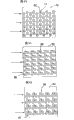
图5-20是本发明的光学方向改变薄膜上分立的光学元件的不同的图案的示意的透视图或顶视图;5-20 are schematic perspective or top views of different patterns of discrete optical elements on optical direction changing films of the present invention;
图5a-5n是方向改变薄膜上分立的光学元件能够采取的不同的几何形状;Figures 5a-5n are different geometries that discrete optical elements on direction changing films can take;
图21是一个光线改向薄膜的示意的透视图,它具有光学沟槽以面对薄膜的一个隅角的一个弯曲的图案延伸跨过薄膜;Figure 21 is a schematic perspective view of a light redirecting film having optical grooves extending across the film in a curved pattern facing a corner of the film;
图22是一个光线改向薄膜的顶视图,它具有光学沟槽的一个图案,面对薄膜的一个边缘的一个中点延伸跨过薄膜,当至一个边缘的距离增加时,其曲率减少;Figure 22 is a top view of a light redirecting film having a pattern of optical grooves extending across the film facing a midpoint of one edge of the film, the curvature of which decreases as the distance from one edge increases;
图23是图22的光学方向改变薄膜的一个端立面图,是由它的左端观察的;Figure 23 is an end elevational view of the optical direction changing film of Figure 22, viewed from its left end;
图24是图22的光线改向薄膜的一个侧立面图;Figure 24 is a side elevational view of the light redirecting film of Figure 22;
图25和26是一个背光板/光发射板组件的一个表面区的放大的示意的不连贯的顶视图,示出在背光板的表面上或表面内形成的不同形式的光学变形器;25 and 26 are enlarged schematic fragmentary top views of a surface region of a backlight/light-emitting panel assembly showing different forms of optical deformers formed on or in the surface of the backlight;
图27和28分别是通过图25和26的光学变形器之一的放大的纵剖面图;Figures 27 and 28 are enlarged longitudinal sectional views through one of the optical deformers of Figures 25 and 26, respectively;
图29和30是通过一个背光板的表面上或表面内形成的另一种光学变形器的放大的示意的纵剖面图;29 and 30 are enlarged schematic longitudinal sectional views of another optical deformer formed on or in the surface of a backlight;
图31-39是背光板表面区的放大的示意的透视图,它具有其它的良好限定形状的各种图案的单独的光学变形器;31-39 are enlarged schematic perspective views of the surface area of the backlight with individual optical deformers of various patterns of other well-defined shapes;
图40是通过一个背光板的表面上或表面内形成的另一种光学变形器的放大的示意的纵剖面图;Figure 40 is an enlarged schematic longitudinal sectional view through another optical deformer formed on or in the surface of a backlight;
图41和42是背光板表面区的放大的示意的顶视图,它具有光学变形器与图37和38所示的类似,沿着表面区的长度和宽度排列为多个直行列;Figures 41 and 42 are enlarged schematic top views of the surface area of a backlight with optical deformers similar to those shown in Figures 37 and 38, arranged in a plurality of straight rows along the length and width of the surface area;
图43和44是背光板表面区的放大的示意的顶视图,它也具有光学变形器与图37和38所示的类似,沿着表面区的长度和宽度排列为交错的行列;Figures 43 and 44 are enlarged schematic top views of the surface area of a backlight, also having optical deformers similar to those shown in Figures 37 and 38, arranged in staggered rows and columns along the length and width of the surface area;
图45和46是背光板表面区的放大的示意的顶视图,它具有在表面区上无序的或变化图案的不同尺寸的光学变形器;Figures 45 and 46 are enlarged schematic top views of the surface area of a backlight having optical deformers of different sizes in random or varying patterns across the surface area;
图47是一个背光板表面区的放大的示意的透视图,示出当变形器至光线输入表面的距离增加或沿着表面区的长度的光线强度增加时,光学变形器的尺寸增加;Fig. 47 is an enlarged schematic perspective view of a backlight surface area showing an increase in the size of the optical deformer as the distance from the deformer to the light input surface increases or the light intensity along the length of the surface area increases;
图48和49是示意的透视图,示出沿着一个背光板表面区的长度和宽度光学变形器的不同的角度取向;以及48 and 49 are schematic perspective views showing different angular orientations of optical deformers along the length and width of a backlight surface area; and
图50和51是放大的透视图,示意地示出由一个聚焦的光源发射的实验的光束如何被良好限定形状的不同的单独的光学变形器反射或折射。Figures 50 and 51 are enlarged perspective views schematically showing how an experimental light beam emitted by a focused light source is reflected or refracted by different individual optical deformers of well-defined shape.
本发明的详细说明Detailed Description of the Invention
图1和2示出按照本发明的一种形式的光线改向薄膜系统1,它包括一个光线改向薄膜2,它能够将由一个背光板BL或其它的光源发射的更多的光线重新分布,接近一个更垂直于薄膜表面的方向。薄膜2可以使用于将来自几乎任何照明用的光源的光线在一个希望的观察角度内重新分布,例如,一个显示器D,比如液晶显示器,使用于膝上型计算机,文字处理器,航空电子学显示器,移动电话,个人数字助理(PDAs)和类似器件,以便使显示器更明亮。液晶显示器可以是任何类型的,包括透射液晶显示器,如图1和2所示,反射的液晶显示器,如图3所示,以及跨反射的液晶显示器,如图4所示。Figures 1 and 2 show a light redirecting
图3中所示的反射的液晶显示器D包括一个背反射器40,邻接背侧面,用于反射进入显示器环境光线离开显示器,以增加显示器的亮度。本发明的光线改向薄膜2放置在邻接反射的液晶显示器的顶面,以使环境光线(或来自前灯的光线)改变方向进入显示器,接近一个更垂直于薄膜平面的方向,用于在一个希望的观察角度内被背反射器反射出,以增加显示器的亮度。光线改向薄膜2可以连接至、叠层至或用其它方式保持就位,顶住液晶显示器的顶面。The reflective liquid crystal display D shown in FIG. 3 includes a
图4中所示的跨反射液晶显示器D包括一个跨反射器T,放置在显示器和背光板BL之间,用于将进入显示器的前面的环境光线反射出显示器,以增加在一个照明环境下的显示器的亮度,以及用于将来自背光板的光线通过跨反射器传送出显示器,以便在黑暗环境中照明显示器。在本实施例中,光线改向薄膜2可以或者放置在邻接显示器的顶面,或者邻接显示器的底面,或者邻接两者,如图4所示,用于将环境光线和/或来自背光板的光线改变方向或重新分布,更垂直于薄膜的平面,以便使光束输出分布更适合于前进通过显示器,以增加显示器的亮度。The trans-reflective liquid crystal display D shown in FIG. 4 includes a trans-reflector T placed between the display and the backlight BL for reflecting ambient light entering the front of the display out of the display to increase the luminance in a lighting environment. The brightness of the display, and is used to send light from the backlight out of the display across the reflectors to illuminate the display in dark environments. In this embodiment, the
光线改向薄膜2包括一个薄的透明的薄膜或基片8,在光线出射表面6上具有良好限定形状的不连续的分立的光学元件5,用于折射入射光线分布,从而使薄膜的出射光线在更垂直于薄膜的表面的方向。The
每个分立的光学元件5具有的宽度和长度比薄膜的宽度和长度小许多倍,以及可以借助在薄膜的出射表面上的凹陷或凸起而形成。这些分立的光学元件5包括至少一个倾斜的表面,用于折射入射光线接近一个垂直于光线出射表面的方向。图5示出在一个薄膜2上的分立的光学元件5的一种图案。这些光学元件可以采用许多不同的形状。例如,图5a示出一种非棱柱的光学元件5,具有总计两个表面10,12,它们都是倾斜的。图5a中所示的表面10之一是平面的,而另一个表面12是弯曲的。再者,两个表面10,12彼此相交,以及也与薄膜的表面相交。代替的方案是,分立的光学元件的两个表面10,12可以是弯曲的,如图5b中所示。代替的方案是,光学元件5可以每个具有仅一个表面是弯曲的和倾斜的,以及与薄膜相交。图5c示出一个这样的光学元件5,呈一个锥形13。图5d示出另一个这样的光学元件,具有一个半球形或拱顶形14。同样,这种光学元件可以具有多于一个倾斜的表面与薄膜相交。Each discrete
图5e示出一个光学元件5,具有总计三个表面,它们全部与薄膜相交和彼此相交。两个表面15和16是弯曲的,而第三表面17是平面的。Figure 5e shows an
图5f示出一个光学元件5,呈一个棱锥形18,并带有四个三角形侧面19,它们彼此相交以及与薄膜相交。棱锥形18的侧面19可以是尺寸和形状相同的,如图5f中所示,或者棱锥形的侧面19可以被延伸这样使侧面具有不同的周边形状,如图5g中所示。同样,光学元件5可以具有任何数目的平面的倾斜的侧面。图5h示出一个光学元件5,带有四个平面的倾斜的侧面20,而图5i示出一个光学元件5,带有八个平面的倾斜的侧面20。Fig. 5f shows an
分立的光学元件5也可以具有多于一个弯曲的和多于一个平面的倾斜的表面,全部与薄膜相交。图5j示出一个光学元件5,具有一对相交的相对倾斜的平面的侧面22以及相对的圆形的或弯曲的末端或侧面23。再者,倾斜的平面的侧面22和弯曲的末端或侧面23可以具有不同的倾斜度,如图5k和5l中所示。此外,光学元件5可以具有至少一个弯曲的表面不与薄膜相交。一个这样的光学元件5示于图5m中,它包括一对相对的倾斜的平面的侧面22,以及相对的圆形的或弯曲的末端或侧面23,以及一个圆形的或弯曲的顶面24,与相对的倾斜的侧面和相对的圆形的末端相交。此外,光学元件5可以沿着它们的长度是弯曲的,如图5n中所示。The discrete
为分立的光学元件5设置平面的和弯曲的表面的组合,比一个带沟槽的薄膜能够提供更大观察区的光线改变方向和重新分布。同样,分立的光学元件的表面的曲率或弯曲区与平面的比率可以改变,以调节薄膜的光线输出的分布,以便改进与薄膜一起使用的显示器的观察区。Providing a combination of planar and curved surfaces for discrete
薄膜2的光线入射表面7可以具有一个光学涂层25(见图2),比如一种抗反射涂层,反射偏光层,一种阻滞涂层或一种偏光层。同样,一个无光泽的或扩散的织构可以设置在光线入射表面7上,这取决于希望的可视的外观。一个无光泽的表面处理产生一个较软的影像,但是不够明亮。本发明的分立的光学元件5的平面的和弯曲的表面的组合能够设计为将投射在其上的一些光线束改变为不同方向,以产生一个较软的影像,而不需要在薄膜的光线入射表面上附加扩散器或无光泽表面处理。The
光线改向薄膜2的分立的光学元件5也希望是彼此搭接为交错的、互锁的和/或交叉的形状,形成一个光学结构,并带有优良的表面覆盖区。以图6,7,13和15为例,示出彼此交错的光学元件5;图8-10示出彼此交叉的光学元件5;以及图11和12示出彼此交叉的光学元件5。再者,光线改向薄膜2的光学元件5的倾斜角度、密度、位置、取向、高度或深度、形状和/或尺寸可以匹配或转动至一个背光板BL或其它的光源的特定的光线输出分布,以便计算内背光板发射的光线的分布的改变,以便在一个希望的观察角度内使由背光板发射的更多的光线重新分布。例如,当至背光板BL,至一个光源26的距离增加,以计算在不同的角度时的背光板发射的光线束的路径R,当至光源的距离增加时,光学元件5与光线改变薄膜2的表面构成的倾斜表面(比如表面10,12)的角度可以改变,如图2所示。同样,背光板BL本身可以设计为在较低角度发射更多的光束,以增加由背光板发射的光线总量以及依靠光线改变薄膜2在一个希望的观察角度内使发射的更多的光线重新分布。从这种方式,光线改向薄膜2的分立的光学元件5可以选择,以便与背光板的光学变形器相结合,以便由系统产生一个优化的输出的光线束角度分布。The discrete
图2,5和9示出分立的光学元件5的不同的图案,全部为相同的高度或深度。而图7、8、10,13和14示出分立的光学元件5的不同的图案,它们为不同的形状、尺寸和高度或深度。Figures 2, 5 and 9 show different patterns of discrete
分立的光学元件5也可以在薄膜2上无序化排列,如图16和17所示,以这样一种方式消除与液晶显示器的像素间距的任何干涉。这样消除了对图1和2所示的光学扩散器层30的需要,以抵抗网纹和类似作用。再者,至少一些分立的光学元件5能够排列为跨过薄膜的分组32,并且至少在每个分组内的一些光学元件5具有不同的尺寸或形状特点,它们集体地产生一个对于每个分组的平均的尺寸或形状特点,它们跨过薄膜改变,如图7、13和15中所示,以获得超出机加工容差的特点值,以抵抗与液晶显示器的像素间距的网格和干涉作用。例如,至少在每个分组32内的一些光学元件5可以具有不同的深度或高度,它们集体地产生对于每一个分组的平均的深度或高度特点,它跨过薄膜改变。同样,至少在每个分组内的一些光学元件5可以具有不同的倾斜角度,它们集体地产生对于每个分组的平均的倾斜角度,它跨过薄膜改变。再者,至少在每个分组内的一些光学元件的一个倾斜表面可以具有不同的宽度和长度,它们集体地产生在每个分组内的平均的宽度和长度特点,它跨过薄膜改变。The discrete
当分立的光学元件5包括平面的和弯曲的表面10,12的一个组合时,弯曲表面12的曲率,或分立的光学元件5的弯曲区与平面区的比率,以及弯曲的和平面的表面的周边的形状可以改变,以调节薄膜的光线输出分布。此外,弯曲表面的曲率,或分立的光学元件的弯曲区与平面区的比率可以改变,以便或多或少地改变在一个平面内前进的光线的方向,它应平行于棱柱的或双凸透镜的带沟槽薄膜的沟槽,部分地或完全地代替对第二层光线改向薄膜的需要。同样,至少一些分立的光学元件可以用彼此不同的角度取向,如图13和16所示,以便使由光源发射的更多的光线在更垂直于薄膜的表面的一个方向上沿两个不同的轴线重新分布,部分地或完全地取代对第二层光线改向薄膜的需要。然而,应该理解,两层这样的光线改向薄膜,每个具有相同的或不同的分立的光学元件图案,可以放置在光源和观察区之间,并且使两层彼此相对转动90°(或其它的角度大于0°和小于90°),从而使在相应的薄膜层上的分立的光学元件将由一个光源发射的在不同的平面方向上前进的更多的光线重新分布在一个更垂直于相应的薄膜的表面的方向上。When the discrete
还有,光线改向薄膜2可以具有光学元件5的一个图案,它在薄膜不同的位置上改变,如图15所示,以便使来自一个背光板或其它光源的光线束的输出分布重新分布,从而使来自不同位置的光线束输出分布重新分布接近一个垂直于薄膜的方向。Also, the
再者,光线改向薄膜的光学元件的性能和图案可以改进以优化光线改向薄膜用于不同类型的光源,它发射不同的光线分布,例如,一种图案用于单灯泡搭接顶部,另一种图案用于双灯泡平板显示器,以及等等。Furthermore, the properties and pattern of the optical elements of the light redirecting film can be improved to optimize the light redirecting film for different types of light sources, which emit different light distributions, for example, one pattern for a single bulb overlapping the top, another One pattern is used for dual bulb flat panel displays, and so on.
图17示出的光学元件5排列为由薄膜2的外边缘至中心的一个径向的图案,以便使一个背光板BL的光线束输出分布重新分布,它接收沿背光板的全部四个侧面的来自冷阴极荧光灯26的光线。Figure 17 shows the
图18示出的光学元件5排列为跨过薄膜2的倾斜的分组32的一个图案,它调节以便使背光板BL的光线束输出分布重新分布,它接收来自一个冷阴极荧光灯26的光线、或者沿背光板的一个输入边缘的一组光发射二极管26的光线。Figure 18 shows
图19示出的光学元件5排列为面对薄膜2的一个隅角的一个径向型图案,它是被一个光发射二极管26照明的隅角。19 shows that the
图20示出的光学元件5排列为面对薄膜2的一个输入边缘的一个中点的径向型图案,以便使一个背光板BL的光线束输出分布重新分布,它被一个单独的光发射二极管26在背光板的一个输入边缘的中点处照明。Figure 20 shows
图21示出的光线改向薄膜2具有光学沟槽35,跨过薄膜以面对薄膜的一个隅角的一个弯曲的图案延伸,以便使背光板BL的光线束输出分布重新分布,它是被一个光发射二极管26照明的隅角。The
图22-24示出的光线改向薄膜2具有光学沟槽35的一个图案,跨过薄膜面对沿着薄膜的一个边缘的一个中点延伸,当至一个边缘的距离增加时,其曲率减少,以便使背光板BL的光线束输出分布重新分布,此边缘被一个光发射二极管26在背光板的一个输入边缘的中点处照明。Figures 22-24 illustrate a
在光线改向薄膜2具有一个光学元件5的一个图案40沿着薄膜的长度改变的情况下,可以提供一个薄膜2的卷材41,它具有一个重复的光学元件图案在其上面,如图15所示,以便允许最适合于一个特定用途的图案的选择区能够由薄膜卷材模压切割。Where the
背光板BL可以是实质上平面的或弯曲的,或者可以是单层的或多层的,以及按希望具有不同的厚度和形状。再者,背光板可以是柔性的或刚性的,以及由各种化合物制造。再者,背光板可以是空心的或充填液体、空气的,或是实心的,以及可以是具有孔或脊岭的。The backlight BL can be substantially planar or curved, or can be single-layered or multi-layered, and have different thicknesses and shapes as desired. Again, backlights can be flexible or rigid, and made from various compounds. Furthermore, the backlight can be hollow or filled with liquid, air, or solid, and can have holes or ridges.
同样,光源26可以是任何适当类型的,例如包括弧光灯、白炽灯,它们同样可以是彩色的、滤光的、或涂漆的,一个透镜末端灯泡、光管、卤素灯、光发射二极管(LED),来自LED的芯片、氖灯泡、冷阴极荧光灯,由遥控源传送的纤维光管、激光器或激光二极管、或任何其它的适当的光源。此外,光源26可以是一个多数的彩色LED,或彩色的辐射源的一个组合,以提供一个希望的彩色的或白色的光线输出分布。例如,一组彩色的灯,比如不同颜色的(例如红色、蓝色、绿色的)LEDs或带有多数的彩色的芯片的单独的LED可以使用于产生白色的光线或借助改变每个单独的彩色灯的强度产生任何的彩色的光线输出分布。Likewise,
光学变形器的一种图案可以按希望设置在背光板BL的一个或两个侧面上,这里使用的术语光学变形器是指一个表面和/或涂层的形状或几何尺寸或表面处理的改变,它引起光线的一部分将由背光板发射。这些变形器能够使用各种方式制造,例如在背光板的选择区内提供一个涂漆的图案、浸蚀的图案、机加工的图案、印刷的图案、热冲压的图案或模压的图案或类似的图案。一种油墨或涂漆图案可以借助下列方式涂覆,例如:衬垫印刷、丝网印刷、喷墨、热转移薄膜过程或类似过程。这些变形器也可以印刷在一个板或薄膜上,它使用于涂覆变形器到背光板上。板或薄膜变成背光板的一个永久的部分,例如,借助连接或其它方法将板或薄膜定位顶住背光板的一个或两个侧面,以产生希望的效果。A pattern of optical deformers may be provided on one or both sides of the backlight BL as desired, the term optical deformers as used herein refers to a change in shape or geometry or surface treatment of a surface and/or coating, It causes a portion of the light to be emitted by the backlight. These deformers can be manufactured using various means such as providing a painted pattern, etched pattern, machined pattern, printed pattern, hot stamped pattern or embossed pattern or similar in selected areas of the backlight. pattern. An ink or paint pattern can be applied by, for example, pad printing, screen printing, inkjet, thermal transfer film process or the like. These deformers can also be printed on a plate or film, which is used to coat the deformers onto a backlight. The plate or film becomes a permanent part of the backlight, for example, by bonding or otherwise positioning the plate or film against one or both sides of the backlight to produce the desired effect.
借助改变背光板的一个区或多个区内的变形器的密度、不透明度或透明度、形状、深度、颜色、面积,折射指数或类型,背光板的光线输出能够被控制。这些变形器可以使用于控制由背光板的一个光线发射区的光线输出的百分比。例如,在希望较少光线输出的表面区可以放置较少的或较小尺寸的变形器。反之,在希望较大光线输出的表面区可以放置较大百分比的或较大尺寸的变形器。By varying the density, opacity or transparency, shape, depth, color, area, index of refraction or type of deformers in one or more regions of the backlight, the light output of the backlight can be controlled. These deformers can be used to control the percentage of light output by a light emitting area of the backlight. For example, fewer or smaller sized deformers can be placed on surface areas where less light output is desired. Conversely, larger percentages or larger size deformers can be placed on surface areas where greater light output is desired.
在背光板的不同的区域内改变变形器的百分比和/或尺寸是需要的,以便提供一个实质上均匀的光线分布。例如,前进通过背光板的光线的数量在接近光源的区域通常比在远离光源的区域大。一种图案的变形器能够使用于调节背光板内光线的改变,例如,随着至光源距离的增加,提供变形器一个更密集的集中,从而导致由背光板的一个更均匀的光线输出分布。这些变形器也可以使用于控制由背光板的输出光束角度分布,以适应一个特定的用途。例如,如果背光板使用于一个液晶显示器的背光板,如果这些变形器(或一个光线改向薄膜2与背光板结合使用)将被背光板发射的光线束以预定的光线束角度投射,则光线输出将更有效,这样使它们以低的损失前进通过液晶显示器。Varying the percentage and/or size of the deformers in different areas of the backlight may be desirable in order to provide a substantially uniform light distribution. For example, the amount of light traveling through the backlight is generally greater in areas close to the light source than in areas farther from the light source. A pattern of deformers can be used to accommodate changes in light within the backlight, eg, providing a denser concentration of the deformers with increasing distance from the light source, resulting in a more uniform distribution of light output from the backlight. These deformers can also be used to control the angular distribution of the output beam from the backlight to suit a particular application. For example, if the backlight is used for the backlight of a liquid crystal display, if these deformers (or a
此外,光学变形器的图案可以使用于调节光线输出的改变,以利于背光板的光线提取。光学变形器的图案可以使用广谱的油漆、油墨、涂料、环氧等印刷在背光板的表面区,由光泽改变至不透明,或两者兼有,以及可以使用半调分离技术以改变变形器的覆盖率。再者,光学变形器的图案可以是多层的或其折射指数是改变的。In addition, the pattern of the optical deformer can be used to adjust the change of the light output to facilitate the light extraction of the backlight panel. Patterns of optical deformers can be printed on the surface area of the backlight using a broad spectrum of paints, inks, coatings, epoxies, etc., changing from glossy to opaque, or both, and halftone separation techniques can be used to change the deformers coverage. Furthermore, the pattern of optical deformers may be multi-layered or its refractive index varied.
光学变形器的印刷图案可以是各种形状的,比如点形、方形、菱形、椭圆形、星形、无序的形状等。再者,最好使用每英寸60线的或更细的印刷图案。这样可使变形器或印刷图案的形状接近在一个特定的用途中可以被人眼观察,从而消除了对梯度或弯曲线的探测,它们在使用较大的光学元件的光线提取图案中是普通的。此外,变形器可以沿着背光板的长度和/或宽度改变形状和/或尺寸。同样,变形器的一个无序的放置图案可以使用于背光板的整个长度和/或宽度。变形器可以具有没有专门角度的形状或图案,以减少网纹或其它干涉作用。产生这些无序的图案的方法的实例是使用随机印刷技术的各种形状的印刷图案,频率模拟半调图案、或无序的点半调图案。The printed pattern of the optical deformer can be in various shapes, such as dots, squares, rhombuses, ellipses, stars, random shapes, etc. Again, it is best to use a printed pattern of 60 lines per inch or finer. This allows the shape of the deformer or printed pattern to be close to being observed by the human eye in one specific application, thereby eliminating the detection of gradient or curved lines that are common in light extraction patterns using larger optics . Additionally, the deformers may change shape and/or size along the length and/or width of the backlight panel. Likewise, a random placement pattern of deformers can be used for the entire length and/or width of the backlight panel. Deformers can have shapes or patterns without specific angles to reduce moiré or other interference effects. Examples of methods of producing these random patterns are printed patterns of various shapes using random printing techniques, frequency analog halftone patterns, or random dot halftone patterns.
再者,变形器可以着色的,以便在背光板内起到颜色校正作用。变形器的颜色也可以通过背光板改变,例如,对相同的或不同的光线输出区提供不同的颜色。Furthermore, the deformers can be tinted to provide color correction within the backlight. The color of the deformer can also be changed by the backlight, for example to provide different colors for the same or different light output areas.
除此之外或代替这些光学变形器也可以使用其它的光学变形器,具有棱柱的或双凸透镜的或横向沟槽,或各种形状的凹陷或升起,使用复杂形状的模压图案,可以是模压的、浸蚀的、冲压的、热成形的、热冲压的或类似的,成形在背光板的一个或多个表面区。这些棱柱的或双凸透镜的表面、凹陷的或升起的表面将引起一部分光线束接触,从而由背光板发射。同样,棱柱的、凹陷的或其它的表面的角度也可以改变,以投射光线在不同的方向上,以便产生一个希望的光线输出分布或效果。In addition to or instead of these optical deformers other optical deformers can be used, with prismatic or lenticular or transverse grooves, or depressions or elevations of various shapes, using embossed patterns of complex shapes, which can be Embossed, etched, stamped, thermoformed, hot stamped, or the like, formed in one or more surface regions of the backlight. These prismatic or lenticular surfaces, recessed or raised surfaces will cause a portion of the beam of light to contact and thus be emitted by the backlight. Likewise, the angle of the prismatic, recessed or other surfaces can be varied to project light in different directions to produce a desired light output distribution or effect.
再者,反射的或折射的表面可具有不带专门的角度的形状或图案,以减少网纹或其它干涉作用。Also, reflective or refractive surfaces may have shapes or patterns without specific angles to reduce moiré or other interference effects.
一个背反射器40可以连接或定位对着背光板BL的一个侧面,如图1和2所示,以便借助将由此侧面发射的光线反射回通过背光板用于发射通过相对的侧面来改进背光板的光线输出效率。此外,一种图案的光学变形器50可以设置在背光板的一个或两个侧面上,如图1和2所示,以便改变光线的路径,从而超过内临界角度和一部分光线是由背光板的一个或两个侧面发射的。A
图25-28示出的光学变形器50可以或者是在相应的背光板表面区52上的单独的凸起51,或者是在这些表面区的单独的凹陷53。在任何一种情况下,每个这种变形器50具有良好限定的形状,包括一个反射或折射表面54,它在一个边缘55处与相应的背光板表面区52相交,以及具有沿其整个长度均匀的倾斜度,以便更精确地控制由每个变形器的光线发射。沿着每个反射/折射表面54的一个周边的边缘部分56是每个变形器50的一个端壁57,它与相应的板表面区52相交,其夹角I大于反射/折射表面54和板表面区52之间的夹角I′(见图27和28),以减少板表面区上端壁的凸起的表面区。这样允许比其它可能的情况下将更多的变形器50放置在板表面区内,这种情况是如果端壁57的凸起的表面区实质上等于或大于反射/折射表面54的凸起的表面区。The
在图25和26内反射/折射表面54的周边边缘部分56和附带的端壁57在横向方向上是弯曲的。同样,在图27和28内变形器50的端壁57示出为实质上垂直于变形器的反射/折射表面54延伸。代替地,此种端壁57可以实质上垂直于板表面区52延伸,如图29和30所示。这样事实上消除了在板表面区52上端壁57的任何的凸起的表面区,从而使在板表面区上的变形器的密度甚至进一步增加。In Figures 25 and 26 the
光学变形器也可以是其它的良好限定的形状,以便由一个板表面区获得一个希望的光线输出分布。图31示出在一个板表面区52上单独的光线提取变形器58,每个包括一个通常的平面的,矩形的反射/折射表面59和附带的均匀倾斜度的端壁60,通过长度和宽度,以及通常的平面的侧壁61。代替地,变形器58,可以具有圆形的或弯曲的侧壁62,如图32所示。The optical deformers can also be of other well-defined shapes in order to obtain a desired light output distribution from a plate surface area. Figure 31 shows individual
图33示出在一个板平面52上单独的光线提取变形器63,每个包括一个平面的、倾斜的三角形的反射/折射表面64和附带的平面的、通常的三角形的侧壁或端壁65。Figure 33 shows individual
图34示出单独的光线提取变形器66,每个包括一个平面的倾斜的反射/折射表面67,具有倾斜的周边边缘部分68和附带的倾斜的端壁69和侧壁70。FIG. 34 shows individual light extraction deformers 66 each comprising a planar sloped reflective/refractive surface 67 with sloped peripheral edge portions 68 and accompanying sloped end walls 69 and side walls 70 .
图35示出单独的光线提取变形器71,它们通常是锥形的,而图36示出单独的光线提取变形器72每个包括一个圆形的反射/折射表面73和圆形的端壁74和圆形的或弯曲的侧壁75,全部掺合在一起。这些附加的表面将撞击在其上的其它光线束反射或折射到不同的方向上,以分散跨过背光板元件BL的光线,以便提供由板元件发射的光线的一个更均匀的分布。Figure 35 shows individual
与单独的变形器的反射/折射表面和端壁及侧壁的形状无关,这些变形器也可以包括平面表面,相对于板表面区52以一种平行的有间距的关系与反射/折射表面和端壁和/或侧壁相交。图37-39示出变形器76,77和78,在一个板表面区上呈单独的凸起的形状,具有代表性的形状分别与图31、32和35的相似,其不同之处是每个变形器相对于板表面区52以平行的有间距的关系与一个平面表面79相交。以类似的方式,图40示出二组变形器80之一,具有单独的凹陷81的形状,位于一个板表面区52内,相对于板表面区52的通常平面表面以平行的有间距的关系与一个平面表面79相交。撞击在此平面表面79上的任何光线束,其内角小于由板表面区52发射光线的临界角,将被平面表面79内部反射而撞击在此平面表面79上的任何光线束,其内角大于由板表面区发射光线的临界角,将被带有最小的光学不连续性的平面表面发射,如图40所示。Regardless of the shape of the reflective/refractive surfaces and end and side walls of the individual deformers, these deformers may also include planar surfaces in a parallel spaced relationship to the reflective/refractive surfaces and The end walls and/or side walls meet. Figures 37-39
在变形器是在板表面区52上的凸起的地方,反射/折射表面以一个角度延伸离开板,其方向通常与来自光源26前进通过板的光线束的方向相反,如图27和29所示。在变形器是在板表面区上的凹陷的地方,反射/折射表面以一个角度延伸进入背光板,其方向通常与来自光源26前进通过板的光线束的方向相同,如图28和30所示。Where the deformities are protrusions on the
与变形器是否是在板表面区52上或其内的凸起或凹陷无关,变形器的反射/折射表面的倾斜度可以改变,以引起撞击在其上面的光线束或者折射出光线发射板,或者通过板反射回以及发射出板的相对的侧面,它可以是浸蚀的,以扩散由其发射的光线,或者涂覆一个光线改向薄膜,以产生一个希望的作用。还有,在板表面区的光学变形器的图案可以是一致的或按希望变化的,以便获得来自板表面区的希望的光线输出分布。图41和42示出变形器76和77,其形状与图37和38所示的相似,排列为一组通常直线的有均匀间距的行列,沿着板表面区52的长度和宽度。而图43和44示出这样的变形器76和77,排列为交错的行列,沿着板表面区的长度彼此搭接。Regardless of whether the deformer is a protrusion or depression on or within the
还有,光学变形器的尺寸,包括宽度、长度和深度或高度,以及角度取向和位置也可以沿着任何给定的板表面区的长度和/或宽度改变,以获得来自板表面区希望的光线输出分布。图45和46示出不同尺寸的变形器58和58′的一个无序的或变化的图案,分别地与图31和32所示的形状相似,排列为在板表面区52上的交错的行列。图47示出变形器77,与图38所示的形状相似,当变形器至光源的距离增加或沿着板表面区的长度和/或宽度的光线的密度减少时,其尺寸增加。图45和46中所示的变形器58和58′排列为跨过板表面的各簇82,并且在每个簇中至少一些变形器具有不同的尺寸或形状特点,它们集体地产生对于每个簇的一个平均的尺寸或形状特点,它跨过板表面改变。例如,在每个簇中至少一些变形器可以具有不同的深度或高度,或不同的倾斜率或取向,它们集体地产生一个平均的深度或高度特点,或倾斜表面的平均的倾斜率或取向,它跨过板表面改变。类似地,在每个簇中至少一些变形器可以具有不同的宽度或长度,它们集体地产生一个平均的宽度或长度特点,它跨过板表面改变。这样允许获得超过机加工容差的希望的尺寸或形状特点,以及还可抵抗网纹和干涉作用。Also, the dimensions of the optical deformers, including width, length, and depth or height, as well as angular orientation and position, can also be varied along the length and/or width of any given panel surface region to obtain desired results from the panel surface region. Light output distribution. Figures 45 and 46 show a random or varying pattern of
图48和49示出沿着一个板表面区52的长度和宽度任何希望形状的变形器85的不同的角度取向。在图48中,变形器排列为直行列86,沿着板表面区的长度,但每个行列中的变形器是取向对着光源26,从而使全部变形器是实质上与由光源发射的光束在一直线上。在图49中,变形器85也是取向对着光源26,与图48相似。此外,在图49中的变形器行列实质上是与光源26径向对准的。48 and 49 illustrate different angular orientations of deformers 85 of any desired shape along the length and width of a
图50和51示出按照本发明的由一个聚焦的光源26发射的示范性的光线束90在前进通过光线发射板元件92时是如何反射的,光源26是插入模压或铸造在光线发射板组件BL的一个光线过渡区91内,直到光线束90撞击在板表面区52上面或其中的良好限定形状的单独的光线提取变形器50,77上,引起由板元件的一个侧面93反射或折射的光线束比由另一个侧面94的多。在图50中,所示的示范性光线束90是变形器50的反射/折射表面54反射在相同的总方向,通过板元件的相同的侧面93射出。而在图51中,所示的光线束90在被反射/折射出板元件的相同的侧面93之前是被变形器77的圆形的侧壁62散射在板元件92内不同的方向上。按照本发明的良好限定形状的单独的光线提取变形器的这样一种图案能够引起60-70%或更多的通过板元件的输入边缘95接收的光线由板元件的相同的侧面发射。50 and 51 illustrate how an exemplary beam of light 90 emitted by a focused
由以上所述可以理解,本发明的光线改向薄膜能使由一个背光板或其它的光源发射的更多的光线重新分布,接近一个更垂直于薄膜的平面的方向。再者,本发明的光线改向薄膜和背光板可以调节或彼此转动,以提供一个系统,其中光线改向薄膜的分立的光学元件与背光板的光学变形器结合工作,以便产生一个由此系统优化的输出光线束角度分布。As can be appreciated from the foregoing, the light redirecting film of the present invention redistributes more of the light emitted by a backlight or other light source, towards a direction more perpendicular to the plane of the film. Furthermore, the light redirecting film and backlight of the present invention can be adjusted or rotated relative to each other to provide a system in which discrete optical elements of the light redirecting film work in conjunction with optical deformers of the backlight to produce a Optimized output beam angular distribution.
虽然本发明根据某些实施例示出和说明,在技术熟练人员阅读和了解本说明书后,明显的是可产生等同的代替和改变。尤其是,有关由上述的部件进行的各种功能,这些术语(包括使用于说明这些部件的对一个“器件”的任何参考),如果没有其它的指示,是有意地对应于任何部件,它进行上述的部件的特定的功能(例如,它是功能上等同的),即使不是结构上等同于公开的部件,它实现本发明的上述的示范性实施例中的功能。此外,虽然本发明的一个特点是相对于仅一个实施例公开的,此特点可以与其它的实施例的一个或多个特点相结合,如果希望和对于任何给定的或特定的用途是有利的。While the invention has been shown and described in terms of certain embodiments, it is obvious that equivalent substitutions and changes may occur to those skilled in the art upon the reading and understanding of this specification. In particular, with respect to the various functions performed by the components described above, these terms (including any reference to a "device" used to describe these components), if not otherwise indicated, are intended to correspond to any component that performs The components described above perform the functions of the above-described exemplary embodiments of the present invention, even if not structurally equivalent to the disclosed components, if they are specified functionally (eg, it is functionally equivalent). Furthermore, although a feature of the invention is disclosed with respect to only one embodiment, that feature may be combined with one or more features of other embodiments, if desired and advantageous for any given or particular use .
Claims (42)
Applications Claiming Priority (2)
| Application Number | Priority Date | Filing Date | Title |
|---|---|---|---|
| US09/909,318 | 2001-07-19 | ||
| US09/909,318 US6752505B2 (en) | 1999-02-23 | 2001-07-19 | Light redirecting films and film systems |
Related Parent Applications (1)
| Application Number | Title | Priority Date | Filing Date |
|---|---|---|---|
| CNB028162102A Division CN1288457C (en) | 2001-07-19 | 2002-07-11 | Light redirecting films and film systems |
Publications (2)
| Publication Number | Publication Date |
|---|---|
| CN1952701A CN1952701A (en) | 2007-04-25 |
| CN100432717C true CN100432717C (en) | 2008-11-12 |
Family
ID=25427020
Family Applications (2)
| Application Number | Title | Priority Date | Filing Date |
|---|---|---|---|
| CNB2006101321880A Expired - Fee Related CN100432717C (en) | 2001-07-19 | 2002-07-11 | Light Redirecting Films and Film Systems |
| CNB028162102A Expired - Fee Related CN1288457C (en) | 2001-07-19 | 2002-07-11 | Light redirecting films and film systems |
Family Applications After (1)
| Application Number | Title | Priority Date | Filing Date |
|---|---|---|---|
| CNB028162102A Expired - Fee Related CN1288457C (en) | 2001-07-19 | 2002-07-11 | Light redirecting films and film systems |
Country Status (7)
| Country | Link |
|---|---|
| US (11) | US6752505B2 (en) |
| EP (2) | EP2523025A3 (en) |
| JP (1) | JP4349902B2 (en) |
| KR (3) | KR100965681B1 (en) |
| CN (2) | CN100432717C (en) |
| TW (3) | TWI240089B (en) |
| WO (1) | WO2003008860A1 (en) |
Cited By (3)
| Publication number | Priority date | Publication date | Assignee | Title |
|---|---|---|---|---|
| US9733411B2 (en) | 2012-10-31 | 2017-08-15 | Fluxwerx Illumination Inc. | Light extraction elements |
| US10215344B2 (en) | 2012-03-05 | 2019-02-26 | Fluxwerx Illumination Inc. | Light emitting panel assemblies and light guides therefor |
| CN109655958A (en) * | 2018-09-13 | 2019-04-19 | 韩国高智株式会社 | A kind of light guide plate with re-entrant angle shape and the backlight module using the light guide plate |
Families Citing this family (469)
| Publication number | Priority date | Publication date | Assignee | Title |
|---|---|---|---|---|
| US7108414B2 (en) | 1995-06-27 | 2006-09-19 | Solid State Opto Limited | Light emitting panel assemblies |
| US6827456B2 (en) * | 1999-02-23 | 2004-12-07 | Solid State Opto Limited | Transreflectors, transreflector systems and displays and methods of making transreflectors |
| US20050024849A1 (en) * | 1999-02-23 | 2005-02-03 | Parker Jeffery R. | Methods of cutting or forming cavities in a substrate for use in making optical films, components or wave guides |
| US6752505B2 (en) * | 1999-02-23 | 2004-06-22 | Solid State Opto Limited | Light redirecting films and film systems |
| US7364341B2 (en) * | 1999-02-23 | 2008-04-29 | Solid State Opto Limited | Light redirecting films including non-interlockable optical elements |
| IL159320A0 (en) * | 2001-06-12 | 2004-06-01 | Wellstat Therapeutics Corp | Compounds for the treatment of metabolic disorders |
| KR100799156B1 (en) * | 2001-07-13 | 2008-01-29 | 삼성전자주식회사 | Light guide plate, manufacturing method thereof, liquid crystal display device using the same |
| TWI258023B (en) * | 2001-11-07 | 2006-07-11 | Ibm | A prism sheet, a back-light unit using said prism sheet, and a transmission type liquid crystal display device |
| EP2244005A1 (en) * | 2001-12-05 | 2010-10-27 | Rambus International Ltd | Transreflector system |
| DE10201029A1 (en) * | 2002-01-11 | 2003-07-24 | Siemens Ag | display device |
| GB0202169D0 (en) * | 2002-01-30 | 2002-03-20 | Innavisions Ltd | Improvements in or relating to optical data recognition |
| US20050180017A1 (en) * | 2002-04-24 | 2005-08-18 | Kazutaka Hara | Light converging system and transmission liquid crystal display |
| JP2004296215A (en) * | 2003-03-26 | 2004-10-21 | Toyota Industries Corp | Transparent substrate for planar light source, method for manufacturing transparent substrate, planar light source, and liquid crystal display device |
| JP4019886B2 (en) * | 2002-09-30 | 2007-12-12 | オムロン株式会社 | Optical film, surface light source device and liquid crystal display device |
| US7671859B2 (en) * | 2002-11-06 | 2010-03-02 | Continental Automotive Systems Us, Inc. | Thin instrument cluster with anti-reflective coating |
| EP1420462A1 (en) * | 2002-11-13 | 2004-05-19 | Heptagon Oy | Light emitting device |
| JP4436105B2 (en) * | 2002-11-29 | 2010-03-24 | 富士通株式会社 | Reflector, illumination device, light guide plate, and display device |
| US7125131B2 (en) * | 2002-12-06 | 2006-10-24 | General Electric Company | Brightness enhancement film with improved view angle |
| TWI275842B (en) * | 2002-12-20 | 2007-03-11 | Hon Hai Prec Ind Co Ltd | Light guide plate and method of making the same |
| US7417782B2 (en) | 2005-02-23 | 2008-08-26 | Pixtronix, Incorporated | Methods and apparatus for spatial light modulation |
| CN1756976A (en) * | 2003-03-06 | 2006-04-05 | 皇家飞利浦电子股份有限公司 | Collimated scanning backlight device |
| KR100584554B1 (en) * | 2003-03-25 | 2006-05-30 | 삼성전자주식회사 | Projection type image display device |
| US20050052871A1 (en) * | 2003-07-11 | 2005-03-10 | Hon Hai Precision Industry Co., Ltd. | Light-emitting diode and backlight system using the same |
| US20050130759A1 (en) * | 2003-12-12 | 2005-06-16 | Hayden Mark X. | Sports shaft with variable contour |
| KR100971392B1 (en) * | 2003-12-24 | 2010-07-21 | 엘지디스플레이 주식회사 | LCD Display |
| TW200602759A (en) * | 2004-03-03 | 2006-01-16 | Kimoto Kk | Light control film and backlight device using it |
| US7255462B2 (en) * | 2004-03-04 | 2007-08-14 | K-Bridge Electronics Co., Ltd. | Dimmer device for backlight module |
| TWM255146U (en) * | 2004-04-22 | 2005-01-11 | Shih-Chieh Tang | Brightness enhancement film having curved prism units |
| US7286280B2 (en) * | 2004-05-07 | 2007-10-23 | The University Of British Columbia | Brightness enhancement film for backlit image displays |
| US7160017B2 (en) * | 2004-06-03 | 2007-01-09 | Eastman Kodak Company | Brightness enhancement film using a linear arrangement of light concentrators |
| US20050269742A1 (en) * | 2004-06-03 | 2005-12-08 | Wright Thomas S | Method for making tools for micro replication |
| KR101307481B1 (en) | 2004-06-04 | 2013-09-26 | 더 보오드 오브 트러스티스 오브 더 유니버시티 오브 일리노이즈 | Methods and devices for fabricating and assembling printable semiconductor elements |
| US20050276949A1 (en) * | 2004-06-15 | 2005-12-15 | Eastman Kodak Company | Optical film and method of manufacture |
| US7236303B2 (en) | 2004-06-15 | 2007-06-26 | Eastman Kodak Company | Thermoplastic optical feature with high apex sharpness |
| US20050275132A1 (en) * | 2004-06-15 | 2005-12-15 | Eastman Kodak Company | Belt over compliant roller used with molding roller |
| KR20060015174A (en) * | 2004-08-13 | 2006-02-16 | 삼성전자주식회사 | Prism sheet and liquid crystal display device having same |
| KR101085444B1 (en) * | 2004-06-25 | 2011-11-21 | 삼성전자주식회사 | Optical materials, backlight assembly having same, and display device having same |
| TWI300494B (en) * | 2004-07-23 | 2008-09-01 | Hon Hai Prec Ind Co Ltd | Light guiding plate and backlight module using the same |
| KR20060018146A (en) * | 2004-08-23 | 2006-02-28 | 엘지전자 주식회사 | Prism sheet of LCD and backlight unit |
| US7212345B2 (en) * | 2004-09-13 | 2007-05-01 | Eastman Kodak Company | Randomized patterns of individual optical elements |
| JP2006086075A (en) * | 2004-09-17 | 2006-03-30 | Alps Electric Co Ltd | Surface-emitting device, back surface-lighting system and liquid crystal display |
| US7466484B2 (en) * | 2004-09-23 | 2008-12-16 | Rohm And Haas Denmark Finance A/S | Wire grid polarizers and optical elements containing them |
| TWI249257B (en) * | 2004-09-24 | 2006-02-11 | Epistar Corp | Illumination apparatus |
| US7775700B2 (en) * | 2004-10-01 | 2010-08-17 | Rohm And Haas Electronics Materials Llc | Turning film using array of roof prism structures |
| JP2006113271A (en) * | 2004-10-14 | 2006-04-27 | Toppan Printing Co Ltd | Backlight unit for liquid crystal display |
| US20060083004A1 (en) * | 2004-10-15 | 2006-04-20 | Eastman Kodak Company | Flat-panel area illumination system |
| JP2006148036A (en) * | 2004-10-19 | 2006-06-08 | Omron Corp | Light emitting light source and light emitting light source array |
| KR101082904B1 (en) * | 2004-10-25 | 2011-11-11 | 삼성전자주식회사 | Light guide panel, and back light assembly and display device having the same |
| KR20070085643A (en) * | 2004-11-04 | 2007-08-27 | 솔리드 스테이트 옵토 리미티드 | Curved long wedge within optical film |
| US20060103777A1 (en) * | 2004-11-15 | 2006-05-18 | 3M Innovative Properties Company | Optical film having a structured surface with rectangular based prisms |
| EP1666936A1 (en) | 2004-12-02 | 2006-06-07 | Asulab S.A. | Dual illumination function optical device and figurative image formation |
| EP1666933A1 (en) | 2004-12-02 | 2006-06-07 | Asulab S.A. | Dual illumination function optical device and figurative image formation |
| US7320538B2 (en) * | 2004-12-30 | 2008-01-22 | 3M Innovative Properties Company | Optical film having a structured surface with concave pyramid-shaped structures |
| US7416309B2 (en) * | 2004-12-30 | 2008-08-26 | 3M Innovative Properties Company | Optical film having a surface with rounded structures |
| US7220026B2 (en) * | 2004-12-30 | 2007-05-22 | 3M Innovative Properties Company | Optical film having a structured surface with offset prismatic structures |
| CN1808234A (en) * | 2005-01-20 | 2006-07-26 | 鸿富锦精密工业(深圳)有限公司 | Light guide plate |
| GB0502453D0 (en) * | 2005-02-05 | 2005-03-16 | Cambridge Flat Projection | Flat panel lens |
| US9158106B2 (en) | 2005-02-23 | 2015-10-13 | Pixtronix, Inc. | Display methods and apparatus |
| US7304786B2 (en) | 2005-02-23 | 2007-12-04 | Pixtronix, Inc. | Methods and apparatus for bi-stable actuation of displays |
| US7999994B2 (en) | 2005-02-23 | 2011-08-16 | Pixtronix, Inc. | Display apparatus and methods for manufacture thereof |
| US8482496B2 (en) | 2006-01-06 | 2013-07-09 | Pixtronix, Inc. | Circuits for controlling MEMS display apparatus on a transparent substrate |
| US7755582B2 (en) | 2005-02-23 | 2010-07-13 | Pixtronix, Incorporated | Display methods and apparatus |
| US7742016B2 (en) | 2005-02-23 | 2010-06-22 | Pixtronix, Incorporated | Display methods and apparatus |
| US9229222B2 (en) | 2005-02-23 | 2016-01-05 | Pixtronix, Inc. | Alignment methods in fluid-filled MEMS displays |
| US7746529B2 (en) | 2005-02-23 | 2010-06-29 | Pixtronix, Inc. | MEMS display apparatus |
| US7304785B2 (en) | 2005-02-23 | 2007-12-04 | Pixtronix, Inc. | Display methods and apparatus |
| US20070205969A1 (en) | 2005-02-23 | 2007-09-06 | Pixtronix, Incorporated | Direct-view MEMS display devices and methods for generating images thereon |
| US7502159B2 (en) | 2005-02-23 | 2009-03-10 | Pixtronix, Inc. | Methods and apparatus for actuating displays |
| US8159428B2 (en) | 2005-02-23 | 2012-04-17 | Pixtronix, Inc. | Display methods and apparatus |
| US7405852B2 (en) | 2005-02-23 | 2008-07-29 | Pixtronix, Inc. | Display apparatus and methods for manufacture thereof |
| US7616368B2 (en) | 2005-02-23 | 2009-11-10 | Pixtronix, Inc. | Light concentrating reflective display methods and apparatus |
| US7675665B2 (en) | 2005-02-23 | 2010-03-09 | Pixtronix, Incorporated | Methods and apparatus for actuating displays |
| US7271945B2 (en) | 2005-02-23 | 2007-09-18 | Pixtronix, Inc. | Methods and apparatus for actuating displays |
| US9082353B2 (en) | 2010-01-05 | 2015-07-14 | Pixtronix, Inc. | Circuits for controlling display apparatus |
| US8310442B2 (en) | 2005-02-23 | 2012-11-13 | Pixtronix, Inc. | Circuits for controlling display apparatus |
| US8519945B2 (en) | 2006-01-06 | 2013-08-27 | Pixtronix, Inc. | Circuits for controlling display apparatus |
| US9261694B2 (en) | 2005-02-23 | 2016-02-16 | Pixtronix, Inc. | Display apparatus and methods for manufacture thereof |
| EP1877696A1 (en) * | 2005-03-12 | 2008-01-16 | 3M Innovative Properties Company | Illumination device and methods for making the same |
| TWM276217U (en) * | 2005-04-22 | 2005-09-21 | Innolux Display Corp | Backlight module and liquid crystal display |
| TW200638075A (en) * | 2005-04-22 | 2006-11-01 | Hon Hai Prec Ind Co Ltd | Light guide plate and backlight module using the same |
| US20060250707A1 (en) * | 2005-05-05 | 2006-11-09 | 3M Innovative Properties Company | Optical film having a surface with rounded pyramidal structures |
| US20060268558A1 (en) * | 2005-05-24 | 2006-11-30 | Synchrolite, L.P. | Method and apparatus for controlling diffusion and color of a light beam |
| US8596824B2 (en) | 2005-05-24 | 2013-12-03 | Syncrolite, L.P. | Method and apparatus for a scrollable modifier for a light fixture |
| KR100728368B1 (en) * | 2005-05-25 | 2007-06-14 | 엘지전자 주식회사 | Backlight unit of liquid crystal display including conical luminance enhancing film and manufacturing method of conical luminance enhancing film |
| KR100682875B1 (en) * | 2005-06-08 | 2007-02-15 | 삼성전기주식회사 | Light guide plate with multi-cycle pattern and lighting device for display device using same |
| CN101218519B (en) * | 2005-06-09 | 2010-09-08 | 友辉光电股份有限公司 | Optical Substrates with Irregular Prismatic Structures for Reduced Moiré Effects |
| US8641259B2 (en) * | 2006-06-09 | 2014-02-04 | Ubright Optronics Corporation | Luminance enhancement optical substrates with anti-interference-fringe structures |
| US9366875B2 (en) * | 2005-06-09 | 2016-06-14 | Ubright Optronics Corporation | Light directing film |
| JP4457979B2 (en) | 2005-06-13 | 2010-04-28 | セイコーエプソン株式会社 | Backlight unit manufacturing method, backlight unit, electro-optical device, and electronic apparatus |
| DE102005027737B4 (en) * | 2005-06-16 | 2013-03-28 | Saint-Gobain Glass Deutschland Gmbh | Use of a transparent disc with a three-dimensional surface structure as a cover plate for components for the use of sunlight |
| TWI274896B (en) * | 2005-06-30 | 2007-03-01 | Efun Technology Co Ltd | Brightness enhancement film having reinforcing layer |
| JP4329736B2 (en) * | 2005-07-04 | 2009-09-09 | セイコーエプソン株式会社 | Optical substrate, planar illumination device, electro-optical device |
| US20070014020A1 (en) * | 2005-07-13 | 2007-01-18 | Eastman Kodak Company | Low birefringent light redirecting film |
| US20070024994A1 (en) * | 2005-07-29 | 2007-02-01 | 3M Innovative Properties Company | Structured optical film with interspersed pyramidal structures |
| US7537374B2 (en) * | 2005-08-27 | 2009-05-26 | 3M Innovative Properties Company | Edge-lit backlight having light recycling cavity with concave transflector |
| US7815355B2 (en) * | 2005-08-27 | 2010-10-19 | 3M Innovative Properties Company | Direct-lit backlight having light recycling cavity with concave transflector |
| TWI464494B (en) * | 2005-08-27 | 2014-12-11 | 3M新設資產公司 | Lighting components and systems |
| US20070047228A1 (en) * | 2005-08-27 | 2007-03-01 | 3M Innovative Properties Company | Methods of forming direct-lit backlights having light recycling cavity with concave transflector |
| TWI391711B (en) * | 2005-09-13 | 2013-04-01 | 迎輝科技股份有限公司 | Condenser with light guiding structure |
| US20070058391A1 (en) * | 2005-09-14 | 2007-03-15 | Wilson Randall H | Light extraction layer |
| US7663712B2 (en) * | 2005-10-10 | 2010-02-16 | Skc Haas Display Films Co., Ltd. | Backlight unit with linearly reduced divergence having the width of an output aperture vary over the length of a light divergence reduction structure |
| US20070103910A1 (en) * | 2005-11-08 | 2007-05-10 | Eastman Kodak Company | Light redirecting films having multiple layers and an adhesion layer |
| US7459899B2 (en) * | 2005-11-21 | 2008-12-02 | Thermo Fisher Scientific Inc. | Inductively-coupled RF power source |
| WO2007067692A1 (en) * | 2005-12-06 | 2007-06-14 | Ubright Optronics Corporation | Luminance enhancement optical substrates with anti-chatter structures |
| TW200725076A (en) * | 2005-12-29 | 2007-07-01 | Speed Tech Corp | Method of adjusting diffusing and condensing light ability of optical element |
| US20070159845A1 (en) * | 2006-01-12 | 2007-07-12 | Omron Corporation | Surface light source device and apparatus using the same |
| US20070086207A1 (en) * | 2006-01-13 | 2007-04-19 | Optical Research Associates | Display systems including light enhancing structures with arrays of elongate features |
| US7674028B2 (en) * | 2006-01-13 | 2010-03-09 | Avery Dennison Corporation | Light enhancing structures with multiple arrays of elongate features of varying characteristics |
| US7866871B2 (en) * | 2006-01-13 | 2011-01-11 | Avery Dennison Corporation | Light enhancing structures with a plurality of arrays of elongate features |
| CN101000387A (en) * | 2006-01-14 | 2007-07-18 | 鸿富锦精密工业(深圳)有限公司 | Prism and backlight module using the prism |
| CN101025516A (en) * | 2006-02-23 | 2007-08-29 | 鸿富锦精密工业(深圳)有限公司 | Backlight module |
| US8526096B2 (en) | 2006-02-23 | 2013-09-03 | Pixtronix, Inc. | Mechanical light modulators with stressed beams |
| CN100468089C (en) * | 2006-03-03 | 2009-03-11 | 鸿富锦精密工业(深圳)有限公司 | Prism sheet and backlight module using the prism sheet |
| KR101234098B1 (en) * | 2006-03-21 | 2013-02-19 | 삼성디스플레이 주식회사 | Optical sheet, backlight assembly and display device having the same |
| US20070223252A1 (en) * | 2006-03-24 | 2007-09-27 | Junwon Lee | Illumination apparatus and film |
| CN100498389C (en) * | 2006-03-25 | 2009-06-10 | 鸿富锦精密工业(深圳)有限公司 | Light conducting plate and back light module |
| US20080081132A1 (en) * | 2006-03-30 | 2008-04-03 | Bourdelais Robert P | Light redirecting film having surface nano-nodules |
| JP2007273091A (en) * | 2006-03-30 | 2007-10-18 | Fujitsu Ltd | Prism light guide plate, lighting device and electronic device |
| JP2007280635A (en) * | 2006-04-03 | 2007-10-25 | Hitachi Displays Ltd | Surface light source device and liquid crystal display device using the same |
| FR2900220B1 (en) * | 2006-04-24 | 2008-07-18 | Valeo Vision Sa | LIGHTING OR SIGNALING DEVICE WITH DEPTH EFFECT. |
| KR100751519B1 (en) * | 2006-05-08 | 2007-08-23 | 미래나노텍(주) | Back light assembly of the liquid crystal display device provided with the optical sheet and the optical sheet |
| US7677146B2 (en) * | 2006-05-10 | 2010-03-16 | 3M Innovative Properties Company | Cutting tool using one or more machined tool tips in a continuous or interrupted cut fast tool servo |
| US7842376B2 (en) * | 2006-05-24 | 2010-11-30 | Zhijian Lu | Diffusers and methods of manufacture |
| US20070279935A1 (en) * | 2006-05-31 | 2007-12-06 | 3M Innovative Properties Company | Flexible light guide |
| US7876489B2 (en) | 2006-06-05 | 2011-01-25 | Pixtronix, Inc. | Display apparatus with optical cavities |
| TW200745490A (en) * | 2006-06-07 | 2007-12-16 | Jeng Shiang Prec Ind Co Ltd | Light guide plate |
| RU2006119965A (en) * | 2006-06-07 | 2007-12-27 | Самсунг Электроникс Ко., Лтд. (KR) | OPTICAL FILM |
| US7670726B2 (en) * | 2006-07-20 | 2010-03-02 | Zhijian Lu | Optical diffusers, photomasks and their methods of fabrication |
| US20080024870A1 (en) * | 2006-07-27 | 2008-01-31 | Bourdelais Robert P | Light-redirecting film containing optical modification layer |
| US20080032096A1 (en) * | 2006-08-07 | 2008-02-07 | Eastman Kodak Company | Microstructured film containing polysulfone polymer |
| US7498534B2 (en) * | 2006-08-30 | 2009-03-03 | 3M Innovative Properties Company | Keypad light guide |
| US7643218B2 (en) * | 2006-08-31 | 2010-01-05 | Skc Haas Display Films Co., Ltd. | Light redirecting film having varying optical elements |
| US8525402B2 (en) * | 2006-09-11 | 2013-09-03 | 3M Innovative Properties Company | Illumination devices and methods for making the same |
| US8581393B2 (en) | 2006-09-21 | 2013-11-12 | 3M Innovative Properties Company | Thermally conductive LED assembly |
| US7481563B2 (en) * | 2006-09-21 | 2009-01-27 | 3M Innovative Properties Company | LED backlight |
| EP2080045A1 (en) | 2006-10-20 | 2009-07-22 | Pixtronix Inc. | Light guides and backlight systems incorporating light redirectors at varying densities |
| US20080101759A1 (en) * | 2006-10-26 | 2008-05-01 | K Laser Technology, Inc. | Prism matrix with random phase structures |
| US20080106899A1 (en) * | 2006-11-03 | 2008-05-08 | Entire Technology Co., Ltd. | Direct backlight module |
| EP2101975A2 (en) | 2006-11-03 | 2009-09-23 | Trustees of Tufts College | Biopolymer sensor and method of manufacturing the same |
| JP2010509644A (en) | 2006-11-03 | 2010-03-25 | トラスティーズ オブ タフツ カレッジ | Biopolymer optical waveguide and manufacturing method thereof |
| EP2650112B1 (en) | 2006-11-03 | 2016-08-24 | Trustees Of Tufts College | Nanopatterned biopolymer optical device and method of manufacturing the same |
| WO2008118211A2 (en) | 2006-11-03 | 2008-10-02 | Trustees Of Tufts College | Biopolymer photonic crystals and method of manufacturing the same |
| JP4880697B2 (en) * | 2006-11-09 | 2012-02-22 | シャープ株式会社 | Prism sheet and liquid crystal display device |
| CN101191870A (en) * | 2006-11-24 | 2008-06-04 | 鸿富锦精密工业(深圳)有限公司 | Optical plate and its preparation method |
| US7661849B2 (en) * | 2006-11-27 | 2010-02-16 | Ping Sun Patrick Lo | Illuminated apparatus |
| CN101191945B (en) * | 2006-11-29 | 2010-11-10 | 清华大学 | Backlight module |
| CN101191849A (en) * | 2006-12-01 | 2008-06-04 | 鸿富锦精密工业(深圳)有限公司 | optical board |
| CN101196584A (en) * | 2006-12-08 | 2008-06-11 | 鸿富锦精密工业(深圳)有限公司 | optical board |
| US7628100B2 (en) * | 2007-01-05 | 2009-12-08 | 3M Innovative Properties Company | Cutting tool using one or more machined tool tips with diffractive features in a continuous or interrupted cut fast tool servo |
| KR100903028B1 (en) * | 2007-01-15 | 2009-06-18 | 제일모직주식회사 | LGP for backlight unit of liquid crystal display including wedge back prism |
| US9176318B2 (en) | 2007-05-18 | 2015-11-03 | Pixtronix, Inc. | Methods for manufacturing fluid-filled MEMS displays |
| US7852546B2 (en) | 2007-10-19 | 2010-12-14 | Pixtronix, Inc. | Spacers for maintaining display apparatus alignment |
| US20080188277A1 (en) | 2007-02-01 | 2008-08-07 | Ritter Janice E | Electronic Game Device And Method Of Using The Same |
| US20100184499A1 (en) * | 2007-02-01 | 2010-07-22 | Ritter Janice E | Electronic Game Device and Method of Using the Same |
| US7543974B2 (en) * | 2007-03-06 | 2009-06-09 | Skc Haas Display Films Co., Ltd. | Light redirecting film having variable thickness |
| US7530726B2 (en) | 2007-03-06 | 2009-05-12 | Skc Haas Display Films Co., Ltd. | Light redirecting film having discontinuous coating |
| JP5349453B2 (en) * | 2007-04-05 | 2013-11-20 | コーニンクレッカ フィリップス エヌ ヴェ | Light beam shaper |
| CN101295034A (en) * | 2007-04-26 | 2008-10-29 | 鸿富锦精密工业(深圳)有限公司 | Backlight module and its optical board |
| CN101295041B (en) * | 2007-04-27 | 2011-12-21 | 鸿富锦精密工业(深圳)有限公司 | Back light module and optical plate |
| US7733439B2 (en) * | 2007-04-30 | 2010-06-08 | Qualcomm Mems Technologies, Inc. | Dual film light guide for illuminating displays |
| TWI439641B (en) * | 2007-05-20 | 2014-06-01 | 3M Innovative Properties Co | Collimating light injectors for edge-lit backlights |
| CN101681597A (en) * | 2007-05-20 | 2010-03-24 | 3M创新有限公司 | White light backlight source and the like for effectively utilizing colored LED light sources |
| TWI458918B (en) | 2007-05-20 | 2014-11-01 | 3M Innovative Properties Co | Thin hollow backlights with beneficial design characteristics |
| CN101681053B (en) | 2007-05-20 | 2012-03-21 | 3M创新有限公司 | Recirculating backlight with semi-mirror elements |
| CN101681056B (en) | 2007-05-20 | 2013-03-27 | 3M创新有限公司 | Backlight and display system using same |
| US20080295327A1 (en) * | 2007-06-01 | 2008-12-04 | 3M Innovative Properties Company | Flexible circuit |
| CN101334554B (en) * | 2007-06-28 | 2011-07-27 | 鸿富锦精密工业(深圳)有限公司 | Backlight module group and its optical plate |
| CN101339327B (en) * | 2007-07-04 | 2011-09-28 | 鸿富锦精密工业(深圳)有限公司 | Backlight module group and its optical plate |
| CN101354450B (en) * | 2007-07-26 | 2012-03-14 | 鸿富锦精密工业(深圳)有限公司 | Optical plate and manufacture method thereof |
| CN101354451A (en) * | 2007-07-26 | 2009-01-28 | 鸿富锦精密工业(深圳)有限公司 | Optical plate and its preparation method |
| US20090041553A1 (en) * | 2007-08-06 | 2009-02-12 | 3M Innovative Properties Company | Fly-cutting system and method, and related tooling and articles |
| CN101363935A (en) * | 2007-08-06 | 2009-02-11 | 鸿富锦精密工业(深圳)有限公司 | Liquid crystal display device and its optical plate |
| CN101363926B (en) * | 2007-08-07 | 2011-11-16 | 鸿富锦精密工业(深圳)有限公司 | LCD device and prismatic lens thereof |
| CN101363927A (en) * | 2007-08-07 | 2009-02-11 | 鸿富锦精密工业(深圳)有限公司 | Prism sheet and liquid crystal display device using the prism sheet |
| CN101373229B (en) * | 2007-08-20 | 2011-02-09 | 鸿富锦精密工业(深圳)有限公司 | Liquid crystal display device and prism sheet thereof |
| CN101393281B (en) * | 2007-09-21 | 2011-02-09 | 鸿富锦精密工业(深圳)有限公司 | Backlight module and its prism sheet |
| TWI451138B (en) * | 2007-10-05 | 2014-09-01 | Hon Hai Prec Ind Co Ltd | Prism sheet and liquid crystal display device using the same |
| GB2455057A (en) | 2007-10-08 | 2009-06-03 | Sharp Kk | Prismatic curved sheet optical device for use in a curved display |
| CN101420829B (en) * | 2007-10-25 | 2011-09-21 | 深圳富泰宏精密工业有限公司 | Metal case and manufacturing method therefor |
| US7669508B2 (en) * | 2007-10-29 | 2010-03-02 | 3M Innovative Properties Company | Cutting tool using one or more machined tool tips with diffractive features |
| JP4935627B2 (en) * | 2007-10-30 | 2012-05-23 | ソニー株式会社 | OPTICAL ELEMENT AND METHOD FOR PRODUCING OPTICAL ELEMENT MANUFACTURING MASTER |
| JP2011504421A (en) | 2007-11-05 | 2011-02-10 | トラスティーズ オブ タフツ カレッジ | Fabrication of silk fibroin photonic structure by nanocontact imprinting |
| WO2009061947A1 (en) * | 2007-11-07 | 2009-05-14 | Ashoff Richard D | Illuminated tile systems and methods for manufacturing the same |
| TW200921006A (en) * | 2007-11-12 | 2009-05-16 | Whe-Yi Chiang | Lighting device |
| EP2212723A4 (en) * | 2007-11-19 | 2014-08-06 | 3M Innovative Properties Co | Articles and methods of making articles having a concavity or convexity |
| US20090129098A1 (en) * | 2007-11-19 | 2009-05-21 | Yi-Fang Lin | Light guide plate having multi-facet reflection structure |
| US20090147361A1 (en) * | 2007-12-07 | 2009-06-11 | 3M Innovative Properties Company | Microreplicated films having diffractive features on macro-scale features |
| CN101452144A (en) * | 2007-12-07 | 2009-06-10 | 旭丽电子(广州)有限公司 | Optical assembly |
| CN101457901B (en) * | 2007-12-14 | 2010-09-29 | 富士迈半导体精密工业(上海)有限公司 | Light field adjustment device and lighting device using the light field adjustment device |
| US20090154198A1 (en) * | 2007-12-14 | 2009-06-18 | Joo Hoon Lee | Reflection type display apparatus |
| TWI352222B (en) * | 2008-01-16 | 2011-11-11 | Coretronic Corp | Light-collimating film |
| WO2009092013A1 (en) | 2008-01-18 | 2009-07-23 | Omnicolor, L.P. | Pattern generator for a light fixture |
| US8848132B2 (en) * | 2008-02-07 | 2014-09-30 | 3M Innovative Properties Company | Hollow backlight with structured films |
| WO2009105450A1 (en) * | 2008-02-22 | 2009-08-27 | 3M Innovative Properties Company | Backlights having selected output light flux distributions and display systems using same |
| KR20100127283A (en) * | 2008-03-19 | 2010-12-03 | 아이2아이씨 코포레이션 | Directional Light Source Using Refractive and Reflective Optics |
| US8851734B2 (en) * | 2008-03-27 | 2014-10-07 | Skc Haas Display Films Co., Ltd. | Light guiding film having light extraction features |
| WO2009146055A2 (en) * | 2008-04-02 | 2009-12-03 | 3M Innovative Properties Company | Methods and systems for fabricating optical films having superimposed features |
| WO2009124107A1 (en) | 2008-04-02 | 2009-10-08 | 3M Innovative Properties Company | Light directing film and method for making the same |
| US8248560B2 (en) | 2008-04-18 | 2012-08-21 | Pixtronix, Inc. | Light guides and backlight systems incorporating prismatic structures and light redirectors |
| CN102016399B (en) * | 2008-06-04 | 2012-11-07 | 夏普株式会社 | Light guide, lighting device and liquid crystal display device |
| KR20110019388A (en) * | 2008-06-04 | 2011-02-25 | 쓰리엠 이노베이티브 프로퍼티즈 컴파니 | Hollow backlight with oblique light source |
| US8002435B2 (en) * | 2008-06-13 | 2011-08-23 | Philips Electronics Ltd Philips Electronique Ltee | Orientable lens for an LED fixture |
| US7766509B1 (en) | 2008-06-13 | 2010-08-03 | Lumec Inc. | Orientable lens for an LED fixture |
| EP2307054A4 (en) * | 2008-06-18 | 2013-02-06 | Tufts College | HOLOGRAPHIC PRODUCTS EDIBLE IN SILK |
| CN201237121Y (en) * | 2008-06-25 | 2009-05-13 | 武良举 | Embedded lamp with auxiliary lighting function |
| CN101619836A (en) * | 2008-06-30 | 2010-01-06 | 鸿富锦精密工业(深圳)有限公司 | Backlight module and diffusion plate thereof |
| CN101631149B (en) * | 2008-07-17 | 2012-09-26 | 比亚迪股份有限公司 | Mobile phone and method for manufacturing backlight module of shell thereof |
| US8462292B2 (en) * | 2008-07-31 | 2013-06-11 | Rambus Delaware Llc | Optically transmissive substrates and light emitting assemblies and methods of making same, and methods of displaying images using the optically transmissive substrates and light emitting assemblies |
| US8520285B2 (en) | 2008-08-04 | 2013-08-27 | Pixtronix, Inc. | Methods for manufacturing cold seal fluid-filled display apparatus |
| US7920317B2 (en) | 2008-08-04 | 2011-04-05 | Pixtronix, Inc. | Display with controlled formation of bubbles |
| US8358266B2 (en) * | 2008-09-02 | 2013-01-22 | Qualcomm Mems Technologies, Inc. | Light turning device with prismatic light turning features |
| WO2010027942A1 (en) * | 2008-09-02 | 2010-03-11 | Qualcom Mems Technologies, Inc. | Light turning device with prismatic light turning features |
| US9004713B2 (en) | 2008-09-10 | 2015-04-14 | Man-D-Tec, Inc. | Illumination assembly |
| US8092035B2 (en) * | 2008-09-10 | 2012-01-10 | Man-D-Tec | Illumination method and assembly |
| US8317360B2 (en) * | 2008-09-18 | 2012-11-27 | Guardian Industries Corp. | Lighting system cover including AR-coated textured glass, and method of making the same |
| US20100080007A1 (en) * | 2008-09-29 | 2010-04-01 | Ping-Han Chuang | Light distribution board having improved grating structure including a plurality of light gratings each with multiple focuses |
| US8886334B2 (en) | 2008-10-07 | 2014-11-11 | Mc10, Inc. | Systems, methods, and devices using stretchable or flexible electronics for medical applications |
| US8372726B2 (en) | 2008-10-07 | 2013-02-12 | Mc10, Inc. | Methods and applications of non-planar imaging arrays |
| US8389862B2 (en) | 2008-10-07 | 2013-03-05 | Mc10, Inc. | Extremely stretchable electronics |
| WO2010042653A1 (en) | 2008-10-07 | 2010-04-15 | Mc10, Inc. | Catheter balloon having stretchable integrated circuitry and sensor array |
| US8097926B2 (en) | 2008-10-07 | 2012-01-17 | Mc10, Inc. | Systems, methods, and devices having stretchable integrated circuitry for sensing and delivering therapy |
| US8169679B2 (en) | 2008-10-27 | 2012-05-01 | Pixtronix, Inc. | MEMS anchors |
| DE102008055865A1 (en) | 2008-11-05 | 2010-05-12 | Lisa Dräxlmaier GmbH | Sensing device for operating electrical load in vehicle, particularly for integration in body trim, has fixed elastically deformed actuating surface, and flat elastically deformed light guide for illuminating symbolism |
| US20100129617A1 (en) * | 2008-11-21 | 2010-05-27 | Corrigan Thomas R | Laser ablation tooling via sparse patterned masks |
| US20100128351A1 (en) * | 2008-11-21 | 2010-05-27 | 3M Innovative Properties Company | Curved sided cone structures for controlling gain and viewing angle in an optical film |
| US8317352B2 (en) | 2008-12-11 | 2012-11-27 | Robert Saccomanno | Non-invasive injection of light into a transparent substrate, such as a window pane through its face |
| TWI514421B (en) * | 2008-12-31 | 2015-12-21 | Ind Tech Res Inst | Transparent conducting composite film with anti-reflection |
| US8231257B2 (en) | 2009-01-13 | 2012-07-31 | Qualcomm Mems Technologies, Inc. | Large area light panel and screen |
| US8246212B2 (en) * | 2009-01-30 | 2012-08-21 | Koninklijke Philips Electronics N.V. | LED optical assembly |
| EP2396276B1 (en) | 2009-02-12 | 2016-08-31 | Trustees Of Tufts College | Nanoimprinting of silk fibroin structures for biomedical and biophotonic applications |
| KR101294851B1 (en) * | 2009-04-01 | 2013-08-08 | 엘지디스플레이 주식회사 | Liquid crystal display and driving method of thereof |
| CN101852876B (en) * | 2009-04-02 | 2012-06-13 | 财团法人工业技术研究院 | Composite optical film and surface light source module |
| BRPI1007601A2 (en) | 2009-04-24 | 2016-02-16 | 3M Innovative Properties Co | "light set" |
| US8530841B2 (en) * | 2009-05-18 | 2013-09-10 | Nec Corporation | Infrared sensor, electronic device, and manufacturing method of infrared sensor |
| US20100302218A1 (en) | 2009-05-29 | 2010-12-02 | Qualcomm Mems Technologies, Inc. | Illumination devices and methods of fabrication thereof |
| US20100309409A1 (en) * | 2009-06-03 | 2010-12-09 | Starkey Kurt R | Light emitting assemblies having defined regions of different brightness |
| CN101956925B (en) * | 2009-07-16 | 2012-12-26 | 瀚宇彩晶股份有限公司 | Backlight module and electronic device |
| AU2010307268B2 (en) | 2009-07-20 | 2015-05-14 | Tufts University/Trustees Of Tufts College | All-protein implantable, resorbable reflectors |
| EP3121509B1 (en) | 2009-07-21 | 2018-06-13 | 3M Innovative Properties Company | Light assembly |
| KR20110016423A (en) * | 2009-08-11 | 2011-02-17 | 유브라이트 옵트로닉스 코포레이션 | Brightness-enhanced optical substrate with interference fringe prevention structure |
| DE102009038469B4 (en) * | 2009-08-21 | 2015-02-12 | Advanced Display Technology Ag | Display element and method for driving a display element |
| WO2011026101A2 (en) | 2009-08-31 | 2011-03-03 | Trustees Of Tufts College | Silk transistor devices |
| US20110070398A1 (en) * | 2009-09-18 | 2011-03-24 | 3M Innovative Properties Company | Laser ablation tooling via distributed patterned masks |
| US9723122B2 (en) | 2009-10-01 | 2017-08-01 | Mc10, Inc. | Protective cases with integrated electronics |
| JP5898085B2 (en) | 2009-10-24 | 2016-04-06 | スリーエム イノベイティブ プロパティズ カンパニー | Soaked asymmetric reflector with reduced color |
| WO2011050982A1 (en) | 2009-10-29 | 2011-05-05 | Arno Martin Sauer | Plate for producing an led-illuminated sign |
| CN102072433B (en) * | 2009-11-23 | 2012-11-21 | 群康科技(深圳)有限公司 | Backlight module and optical board thereof |
| TWI409544B (en) * | 2009-11-23 | 2013-09-21 | Global Lighting Technologies | Method and Structure of Luminous Homogenization of Backlight Module |
| TW201118692A (en) * | 2009-11-27 | 2011-06-01 | Coretronic Corp | Light guide apparatus and optical touch display apparatus |
| JP5152928B2 (en) * | 2009-12-03 | 2013-02-27 | 株式会社エス・ケー・ジー | Partition plate device |
| US9936574B2 (en) | 2009-12-16 | 2018-04-03 | The Board Of Trustees Of The University Of Illinois | Waterproof stretchable optoelectronics |
| US8666471B2 (en) | 2010-03-17 | 2014-03-04 | The Board Of Trustees Of The University Of Illinois | Implantable biomedical devices on bioresorbable substrates |
| US10918298B2 (en) | 2009-12-16 | 2021-02-16 | The Board Of Trustees Of The University Of Illinois | High-speed, high-resolution electrophysiology in-vivo using conformal electronics |
| US10441185B2 (en) | 2009-12-16 | 2019-10-15 | The Board Of Trustees Of The University Of Illinois | Flexible and stretchable electronic systems for epidermal electronics |
| KR101587551B1 (en) * | 2009-12-17 | 2016-01-21 | 삼성전자주식회사 | 3 3 Waveguide plate for 3D image display and 3D image display apparatus employing the same |
| CN102667543B (en) | 2009-12-21 | 2016-08-31 | 3M创新有限公司 | Transflective articles and lamp assemblies |
| TWI400531B (en) * | 2009-12-23 | 2013-07-01 | Innolux Corp | Optical plate and backlight module using the same |
| US20110157867A1 (en) * | 2009-12-28 | 2011-06-30 | Chi-Feng Lin | Diffusion plate having microstructures with two lengthy and slant faces applied for backlight module and optical device |
| JP2013519122A (en) | 2010-02-02 | 2013-05-23 | ピクストロニックス・インコーポレーテッド | Circuit for controlling a display device |
| DE102010002282A1 (en) | 2010-02-24 | 2011-08-25 | Lisa Dräxlmaier GmbH, 84137 | Interior trim part and outer trim part of a vehicle with an ultrasonic sensor |
| US20110278147A1 (en) * | 2010-05-13 | 2011-11-17 | Global Lighting Technologies, Inc. | Keyboard device |
| TW201142384A (en) * | 2010-05-18 | 2011-12-01 | Global Lighting Technolog Inc | Light guide panel, front-light module and reflctive display apparatus |
| GB201008599D0 (en) | 2010-05-24 | 2010-07-07 | Design Led Products Ltd | Light guide device |
| JP5803320B2 (en) * | 2010-09-14 | 2015-11-04 | 大日本印刷株式会社 | Surface light source device, liquid crystal display device, and optical member |
| TW201213970A (en) * | 2010-09-30 | 2012-04-01 | Global Lighting Technolog Inc | Backlight module and liquid crystal display |
| US9200781B2 (en) * | 2010-10-06 | 2015-12-01 | Shoot The Moon Products Ii, Llc | Light emitting decorative panels |
| US9134008B2 (en) | 2010-10-06 | 2015-09-15 | Shoot The Moon Products Ii, Llc | Light emitting decorative panels |
| KR101226936B1 (en) * | 2010-11-10 | 2013-01-30 | 주식회사 엘지화학 | Optical member and method for manufacturing the same and backlight using the optical member, and method for manufacturing the same |
| TWI421596B (en) * | 2010-12-31 | 2014-01-01 | Au Optronics Corp | Three-dimensional display apparatus and backlight module thereof |
| CN102081188A (en) * | 2011-01-10 | 2011-06-01 | 苏州向隆塑胶有限公司 | Light guide plate and manufacturing method thereof |
| TWI442110B (en) * | 2011-01-26 | 2014-06-21 | Coretronic Corp | Light guide plate and light source module |
| CN102062894A (en) * | 2011-02-22 | 2011-05-18 | 苏州向隆塑胶有限公司 | Optical board |
| TWI417584B (en) * | 2011-03-03 | 2013-12-01 | Futis Internat Ltd | Method for forming a microretarder film |
| JP2012195220A (en) * | 2011-03-17 | 2012-10-11 | Enplas Corp | Surface light source device |
| US20120274874A1 (en) * | 2011-04-29 | 2012-11-01 | Shenzhen China Star Optoelectronics Technology Co. Ltd. | Backlight Module and Liquid Crystal Display Device |
| US8864360B2 (en) | 2011-05-06 | 2014-10-21 | Rambus Delaware Llc | Lighting assembly |
| EP2707765A1 (en) | 2011-05-13 | 2014-03-19 | 3M Innovative Properties Company | Back-lit transmissive display having variable index light extraction layer |
| US9765934B2 (en) | 2011-05-16 | 2017-09-19 | The Board Of Trustees Of The University Of Illinois | Thermally managed LED arrays assembled by printing |
| EP2712491B1 (en) | 2011-05-27 | 2019-12-04 | Mc10, Inc. | Flexible electronic structure |
| EP2713863B1 (en) | 2011-06-03 | 2020-01-15 | The Board of Trustees of the University of Illionis | Conformable actively multiplexed high-density surface electrode array for brain interfacing |
| TW201303223A (en) * | 2011-06-09 | 2013-01-16 | Rambus Inc | Lighting assembly |
| TW201305487A (en) * | 2011-07-13 | 2013-02-01 | Rambus Inc | Lighting assembly with controlled configurable light redirection |
| WO2013022606A1 (en) * | 2011-08-05 | 2013-02-14 | Rambus Inc. | Lighting assembly with configurable illumination profile |
| KR20130025638A (en) * | 2011-09-02 | 2013-03-12 | 엘지이노텍 주식회사 | Optical sheet |
| WO2013058961A1 (en) | 2011-10-20 | 2013-04-25 | Rambus Inc. | Modular light-emitting panel assembly |
| KR20130047334A (en) * | 2011-10-31 | 2013-05-08 | 엘지이노텍 주식회사 | Lighting member and lighting device comprising the same |
| CN102410474A (en) * | 2011-11-07 | 2012-04-11 | 苏州艾隆科技有限公司 | LED (light-emitting diode) backlight sheet of intelligent medicine framework |
| US20140140091A1 (en) * | 2012-11-20 | 2014-05-22 | Sergiy Victorovich Vasylyev | Waveguide illumination system |
| KR101979354B1 (en) | 2011-12-01 | 2019-08-29 | 더 보오드 오브 트러스티스 오브 더 유니버시티 오브 일리노이즈 | Transient devices designed to undergo programmable transformations |
| WO2013115864A1 (en) | 2012-02-03 | 2013-08-08 | Rambus Inc. | Center-lit lighting assembly |
| CN103699231B (en) * | 2012-03-13 | 2018-08-07 | 陆明科技公司 | Light guide and keyboard back light |
| US8328403B1 (en) * | 2012-03-21 | 2012-12-11 | Morgan Solar Inc. | Light guide illumination devices |
| WO2013149181A1 (en) | 2012-03-30 | 2013-10-03 | The Board Of Trustees Of The University Of Illinois | Appendage mountable electronic devices conformable to surfaces |
| JP5631920B2 (en) * | 2012-04-04 | 2014-11-26 | 京セラドキュメントソリューションズ株式会社 | Image forming apparatus |
| CN102621624A (en) * | 2012-04-24 | 2012-08-01 | 丹阳博昱科技有限公司 | Light guide sheet including optical micro structure and making method |
| TWI539211B (en) * | 2012-04-30 | 2016-06-21 | 中強光電股份有限公司 | Light guide plate and backlight module using the same |
| CN102681083B (en) * | 2012-05-03 | 2015-07-15 | 丹阳博昱科技有限公司 | Light guide plate with concave microstructure and manufacturing method thereof |
| TWI457663B (en) * | 2012-05-16 | 2014-10-21 | 友達光電股份有限公司 | Backlight module |
| CN103454847B (en) * | 2012-05-29 | 2016-05-18 | 杨文君 | Slab guide display and system |
| EP2685295A1 (en) * | 2012-07-10 | 2014-01-15 | Belux IP AG | Lateral light feed |
| KR101287802B1 (en) * | 2012-07-16 | 2013-07-19 | 주식회사 세코닉스 | A Optical Film Having Pattern Diffused Reflection |
| WO2014055411A1 (en) | 2012-10-01 | 2014-04-10 | Rambus Delaware Llc | Led lamp and led lighting assembly |
| US9638853B2 (en) | 2012-10-08 | 2017-05-02 | Rambus Delaware Llc | Article of manufacture with micro-features of differing surface roughness |
| US9171794B2 (en) | 2012-10-09 | 2015-10-27 | Mc10, Inc. | Embedding thin chips in polymer |
| US9091411B2 (en) | 2012-11-02 | 2015-07-28 | Osram Sylvania Inc. | Illumination techniques and devices |
| KR101481677B1 (en) * | 2012-11-30 | 2015-01-13 | 엘지디스플레이 주식회사 | Back Light Unit and Liquid Crystal Display device Comprising The Same And Fabricating Method thereof |
| US9316780B2 (en) | 2012-11-30 | 2016-04-19 | Rambus Deleware LLC | Lighting assembly with defined angular output |
| TW201425812A (en) * | 2012-12-20 | 2014-07-01 | Wintek Corp | Illumination apparatus |
| CN103901523A (en) * | 2012-12-27 | 2014-07-02 | 鸿富锦精密工业(深圳)有限公司 | Light guide plate |
| CN103912797A (en) * | 2013-01-06 | 2014-07-09 | 纬创资通股份有限公司 | Backlight module |
| US9291320B2 (en) | 2013-01-30 | 2016-03-22 | Cree, Inc. | Consolidated troffer |
| US9366396B2 (en) | 2013-01-30 | 2016-06-14 | Cree, Inc. | Optical waveguide and lamp including same |
| US10436969B2 (en) | 2013-01-30 | 2019-10-08 | Ideal Industries Lighting Llc | Optical waveguide and luminaire incorporating same |
| US9442243B2 (en) | 2013-01-30 | 2016-09-13 | Cree, Inc. | Waveguide bodies including redirection features and methods of producing same |
| US9869432B2 (en) | 2013-01-30 | 2018-01-16 | Cree, Inc. | Luminaires using waveguide bodies and optical elements |
| US9625638B2 (en) | 2013-03-15 | 2017-04-18 | Cree, Inc. | Optical waveguide body |
| US9690029B2 (en) | 2013-01-30 | 2017-06-27 | Cree, Inc. | Optical waveguides and luminaires incorporating same |
| US20140240207A1 (en) * | 2013-02-27 | 2014-08-28 | Motorola Mobility Llc | Low-power display and corresponding lighting apparatus and methods of operation |
| US9134552B2 (en) | 2013-03-13 | 2015-09-15 | Pixtronix, Inc. | Display apparatus with narrow gap electrostatic actuators |
| US9110331B2 (en) | 2013-03-13 | 2015-08-18 | Vizio, Inc. | Ultra-thin backlight for LCD displays through use of field-induced polymer electro luminescence panels including integrated light guide |
| US20140268879A1 (en) * | 2013-03-14 | 2014-09-18 | Panasonic Corporation | Transparent waveguide diffuser for lighting and methods of manufacturing transparent waveguide diffuser |
| US9696022B2 (en) | 2013-03-14 | 2017-07-04 | Mandy Holdings Lllp | Downward illumination assembly |
| US9798072B2 (en) | 2013-03-15 | 2017-10-24 | Cree, Inc. | Optical element and method of forming an optical element |
| US10502899B2 (en) * | 2013-03-15 | 2019-12-10 | Ideal Industries Lighting Llc | Outdoor and/or enclosed structure LED luminaire |
| US10400984B2 (en) | 2013-03-15 | 2019-09-03 | Cree, Inc. | LED light fixture and unitary optic member therefor |
| US9200784B2 (en) | 2013-03-15 | 2015-12-01 | Man-D-Tec, Inc. | Downward illumination assembly |
| US10379278B2 (en) * | 2013-03-15 | 2019-08-13 | Ideal Industries Lighting Llc | Outdoor and/or enclosed structure LED luminaire outdoor and/or enclosed structure LED luminaire having outward illumination |
| US9366799B2 (en) | 2013-03-15 | 2016-06-14 | Cree, Inc. | Optical waveguide bodies and luminaires utilizing same |
| US20150049511A1 (en) * | 2013-03-15 | 2015-02-19 | Cree, Inc. | Waveguide Having Unidirectional Illuminance |
| US9920901B2 (en) | 2013-03-15 | 2018-03-20 | Cree, Inc. | LED lensing arrangement |
| US10209429B2 (en) | 2013-03-15 | 2019-02-19 | Cree, Inc. | Luminaire with selectable luminous intensity pattern |
| US10436970B2 (en) | 2013-03-15 | 2019-10-08 | Ideal Industries Lighting Llc | Shaped optical waveguide bodies |
| JP6136502B2 (en) * | 2013-04-15 | 2017-05-31 | ソニー株式会社 | Lighting device, lighting system |
| TWI472817B (en) * | 2013-04-30 | 2015-02-11 | Radiant Opto Electronics Corp | A light guide means and a backlight module having the light guide means |
| FR3006065B1 (en) * | 2013-05-22 | 2016-09-16 | Valeo Vision | REFLECTIVE PATTERN OPTICAL GUIDE FOR THE PROPAGATION OF A BRIGHT BEAM |
| TWI500985B (en) * | 2013-07-23 | 2015-09-21 | Cheng Tao Lee | Light guide |
| GB201315241D0 (en) | 2013-08-27 | 2013-10-09 | Nano Lit Technologies Ltd | Improvements in or relating to lighting |
| US9933144B2 (en) | 2013-09-20 | 2018-04-03 | Man-D-Tec, Inc. | Light fixture mounting assembly |
| US9453639B2 (en) | 2013-09-24 | 2016-09-27 | Mandy Holdings Lllp | Rectilinear light source for elevator interior |
| KR102125451B1 (en) | 2013-11-15 | 2020-06-22 | 엘지이노텍 주식회사 | Device using same |
| US9651740B2 (en) | 2014-01-09 | 2017-05-16 | Cree, Inc. | Extraction film for optical waveguide and method of producing same |
| KR102264379B1 (en) * | 2014-02-05 | 2021-06-15 | 엘지이노텍 주식회사 | Optical device and lighting device using the same |
| US9645301B2 (en) | 2014-03-28 | 2017-05-09 | Rambus Delaware Llc | Lighting assembly with edge-lit light guide and structured cover |
| EP3748408A1 (en) * | 2014-04-01 | 2020-12-09 | 3M Innovative Properties Company | Asymmetric turning film with multiple light sources |
| US9703031B2 (en) | 2014-04-28 | 2017-07-11 | Rambus Delaware Llc | Light guide and lighting assembly with array of rotated micro-optical elements |
| EP2944866A1 (en) * | 2014-05-12 | 2015-11-18 | SMR Patents S.à.r.l. | Optical unit, display device, rear view device and motor vehicle including the same |
| TWI518387B (en) * | 2014-05-26 | 2016-01-21 | 元太科技工業股份有限公司 | Front light module and display device |
| TWI521297B (en) * | 2014-05-30 | 2016-02-11 | 中強光電股份有限公司 | Wavelength conversion module and illumination system |
| KR20160007695A (en) * | 2014-06-24 | 2016-01-21 | 삼성디스플레이 주식회사 | Back-light assembly and display device having the same |
| TWM487458U (en) * | 2014-06-27 | 2014-10-01 | Taiwan Kangdexin Composite Material Co Ltd | Optical turning film and wide viewing angle liquid crystal display including the same |
| CN104065842A (en) * | 2014-07-04 | 2014-09-24 | 江苏达伦电子股份有限公司 | Wireless illumination system achieving lamp control based on cellphone positioning |
| DE202014103304U1 (en) * | 2014-07-17 | 2015-10-21 | Zumtobel Lighting Gmbh | Luminaire assembly and thus equipped lighting device |
| US9664907B2 (en) * | 2014-07-21 | 2017-05-30 | Applied Materials Israel Ltd. | Optical element for spatial beam shaping |
| WO2016019290A2 (en) * | 2014-07-31 | 2016-02-04 | Rambus Delaware Llc | Light guide and lighting assembly having light redirecting features |
| WO2016019220A1 (en) | 2014-07-31 | 2016-02-04 | Rambus Delaware Llc | Light guide and lighting assembly with array of micro-optical element groupings |
| US9671609B2 (en) * | 2014-08-01 | 2017-06-06 | Sct Technology, Ltd. | Display device and method for reducing moiré effects using the same |
| US9753206B2 (en) * | 2014-08-18 | 2017-09-05 | New Optics, Ltd | Light guide plate, and backlight unit and display device including the same |
| KR20160022215A (en) * | 2014-08-18 | 2016-02-29 | (주)뉴옵틱스 | Display device and light guide plate thereof |
| WO2016054128A1 (en) | 2014-09-30 | 2016-04-07 | Rambus Delaware Llc | Micro-optical element having curved surface and light guide and lighting assembly including same |
| US9801474B2 (en) | 2014-10-01 | 2017-10-31 | True Manufacturing Co., Inc. | Edge-lit door for refrigerator unit |
| US10216285B2 (en) | 2015-02-02 | 2019-02-26 | Microsoft Technology Licensing, Llc | Backlit illumination of electronics |
| WO2016138092A1 (en) | 2015-02-25 | 2016-09-01 | Rambus Delaware Llc | Light guide assembly, housing assembly, and lighting assembly including same |
| US9547118B2 (en) * | 2015-03-07 | 2017-01-17 | Ledyoung Technology Corporation | Light guide panel with an improved light guide structure |
| CN107407818A (en) * | 2015-03-26 | 2017-11-28 | 皇家飞利浦有限公司 | Display device with directional control of output and backlight and light guiding method for such display device |
| KR20160132182A (en) | 2015-05-06 | 2016-11-17 | 삼성디스플레이 주식회사 | Display panel and fabricating mehtod of the same |
| US10634837B2 (en) * | 2015-05-08 | 2020-04-28 | 3M Innovative Properties Company | Lightguide with various shapes and extracting structures |
| BR112017025609A2 (en) | 2015-06-01 | 2018-08-07 | The Board Of Trustees Of The University Of Illinois | miniaturized wireless electronic systems with near field communication capabilities |
| MX2017015587A (en) | 2015-06-01 | 2018-08-23 | Univ Illinois | ALTERNATIVE METHOD FOR UV SENSOR. |
| EP3322931B1 (en) * | 2015-07-15 | 2020-04-22 | CoeLux S.r.l. | Chromatic reflective unit |
| WO2017031035A1 (en) * | 2015-08-14 | 2017-02-23 | Rambus Delaware Llc | Light extracting element having serpentine shape, light redirecting element having serpentine shape, and lighting assembly including the same |
| US10925543B2 (en) | 2015-11-11 | 2021-02-23 | The Board Of Trustees Of The University Of Illinois | Bioresorbable silicon electronics for transient implants |
| WO2017147066A1 (en) * | 2016-02-22 | 2017-08-31 | Lumileds Llc | Asymmetrical light intensity distribution from luminaire |
| EP3427307A4 (en) | 2016-03-08 | 2020-01-01 | Lilibrand LLC | LIGHTING SYSTEM COMPRISING A LENS ASSEMBLY |
| RU2629150C1 (en) * | 2016-03-15 | 2017-08-24 | Общество с ограниченной ответственностью "МеталлЭффект" | Dynamic image forming device and method of its obtaining |
| US20170299797A1 (en) | 2016-04-15 | 2017-10-19 | Rambus Delaware Llc | Lighting assembly with differing light output distribution and/or spectrum output |
| JP6636651B2 (en) | 2016-04-22 | 2020-01-29 | シグニファイ ホールディング ビー ヴィSignify Holding B.V. | Pebble louver |
| US10416377B2 (en) | 2016-05-06 | 2019-09-17 | Cree, Inc. | Luminaire with controllable light emission |
| US11719882B2 (en) | 2016-05-06 | 2023-08-08 | Ideal Industries Lighting Llc | Waveguide-based light sources with dynamic beam shaping |
| US11079619B2 (en) | 2016-05-19 | 2021-08-03 | Reald Spark, Llc | Wide angle imaging directional backlights |
| JP2019520609A (en) * | 2016-06-10 | 2019-07-18 | コーニング インコーポレイテッド | Microstructured and patterned light guide plate and devices including the same |
| JP6645371B2 (en) * | 2016-07-15 | 2020-02-14 | オムロン株式会社 | Optical device and stereoscopic display method |
| TWI726006B (en) * | 2016-07-15 | 2021-05-01 | 日商半導體能源研究所股份有限公司 | Display device, input and output device, data processing device |
| CN106019709A (en) * | 2016-07-25 | 2016-10-12 | 广州创维平面显示科技有限公司 | Liquid crystal module and liquid crystal display screen |
| KR102557311B1 (en) * | 2016-08-08 | 2023-07-20 | 삼성디스플레이 주식회사 | Display apparatus |
| CN108139591B (en) * | 2016-09-20 | 2020-08-14 | 京东方科技集团股份有限公司 | Three-dimensional display panel, three-dimensional display apparatus including the same, and method of manufacturing the same |
| GB2554416A (en) | 2016-09-26 | 2018-04-04 | Design Led Ltd | Illuminated eyewear device |
| US20180088270A1 (en) * | 2016-09-29 | 2018-03-29 | Amazon Technologies, Inc. | Lightguide assembly for electronic display |
| WO2018066912A1 (en) * | 2016-10-05 | 2018-04-12 | 엘지이노텍(주) | Head up display device |
| US10185064B2 (en) | 2016-10-26 | 2019-01-22 | Microsoft Technology Licensing, Llc | Curved edge display with controlled luminance |
| US10223952B2 (en) | 2016-10-26 | 2019-03-05 | Microsoft Technology Licensing, Llc | Curved edge display with controlled distortion |
| WO2018107151A1 (en) | 2016-12-09 | 2018-06-14 | Rambus Delaware Llc | Cluster-shaped light-extracting element |
| EP3551932A1 (en) | 2016-12-12 | 2019-10-16 | CSEM Centre Suisse d'Electronique et de Microtechnique SA - Recherche et Développement | Light emitting device |
| EP3563084A1 (en) * | 2016-12-29 | 2019-11-06 | Corning Incorporated | Microstructured and patterned light guide plates and devices comprising the same |
| US12388056B1 (en) | 2017-01-27 | 2025-08-12 | Korrus, Inc. | Linear lighting systems and processes |
| CN110998880A (en) | 2017-01-27 | 2020-04-10 | 莉莉布兰德有限责任公司 | Lighting system with high color rendering index and uniform flat illumination |
| US20180328552A1 (en) | 2017-03-09 | 2018-11-15 | Lilibrand Llc | Fixtures and lighting accessories for lighting devices |
| DE102017003036A1 (en) * | 2017-03-29 | 2018-10-04 | Singulus Technologies Ag | illuminant |
| US20210199879A1 (en) | 2017-05-08 | 2021-07-01 | Reald Spark, Llc | Optical stack for imaging directional backlights |
| KR20250040099A (en) * | 2017-06-30 | 2025-03-21 | 브라이트뷰 테크놀로지즈 아이엔씨. | Light transmissive structures for redistribution of light and lighting systems including same |
| WO2019028141A1 (en) | 2017-08-01 | 2019-02-07 | Technical Consumer Products, Inc. | Edge-lit light fixture having capabilities for a secondary service |
| US10810914B2 (en) | 2017-08-09 | 2020-10-20 | True Manufacturing Co., Inc. | Illuminating display window and merchandiser display unit comprising same |
| TWI878209B (en) | 2017-09-15 | 2025-04-01 | 美商瑞爾D斯帕克有限責任公司 | Display device and a view angle control optical element for application to a display device |
| EP3707554B1 (en) | 2017-11-06 | 2023-09-13 | RealD Spark, LLC | Privacy display apparatus |
| US10012356B1 (en) | 2017-11-22 | 2018-07-03 | LightLouver LLC | Light-redirecting optical daylighting system |
| KR102461800B1 (en) * | 2017-11-27 | 2022-11-01 | 삼성디스플레이 주식회사 | Color conversion substrate and liquid crystal display device including the same |
| CN118672006A (en) | 2018-01-25 | 2024-09-20 | 瑞尔D斯帕克有限责任公司 | Touch screen for privacy display |
| WO2019147762A1 (en) | 2018-01-25 | 2019-08-01 | Reald Spark, Llc | Reflective optical stack for privacy display |
| JP7495027B2 (en) | 2018-03-22 | 2024-06-04 | リアルディー スパーク エルエルシー | Optical waveguide, backlight device and display device |
| US10768430B2 (en) * | 2018-03-29 | 2020-09-08 | Sharp Kabushiki Kaisha | Display device and head-mounted display |
| TWI702443B (en) * | 2018-04-20 | 2020-08-21 | 奇美實業股份有限公司 | Optical plate, optical structure, backlight module and display device with protrusions |
| US11106086B2 (en) * | 2018-04-20 | 2021-08-31 | Chimei Corporation | Optical plate with protrusions, optical structure, backlight module and display device |
| US11041609B2 (en) | 2018-05-01 | 2021-06-22 | Ecosense Lighting Inc. | Lighting systems and devices with central silicone module |
| WO2020005748A1 (en) | 2018-06-29 | 2020-01-02 | Reald Spark, Llc | Optical stack for privacy display |
| WO2020018552A1 (en) | 2018-07-18 | 2020-01-23 | Reald Spark, Llc | Optical stack for switchable directional display |
| US10739513B2 (en) | 2018-08-31 | 2020-08-11 | RAB Lighting Inc. | Apparatuses and methods for efficiently directing light toward and away from a mounting surface |
| WO2020072643A1 (en) | 2018-10-03 | 2020-04-09 | Reald Spark, Llc | Privacy display control apparatus |
| US10801679B2 (en) | 2018-10-08 | 2020-10-13 | RAB Lighting Inc. | Apparatuses and methods for assembling luminaires |
| CN113167953B (en) | 2018-11-07 | 2023-10-24 | 瑞尔D斯帕克有限责任公司 | Directional display device |
| CH715534A1 (en) * | 2018-11-12 | 2020-05-15 | Regent Beleuchtungskoerper Ag | Optics and table lamp. |
| WO2020131933A1 (en) | 2018-12-17 | 2020-06-25 | Lilibrand Llc | Strip lighting systems which comply with ac driving power |
| WO2020146091A1 (en) | 2019-01-07 | 2020-07-16 | Reald Spark, Llc | Optical stack for privacy display |
| WO2020167680A1 (en) | 2019-02-12 | 2020-08-20 | Reald Spark, Llc | Diffuser for privacy display |
| CN109765725B (en) * | 2019-03-26 | 2021-04-06 | 合肥京东方光电科技有限公司 | Collimation film, collimation backlight module, display module and display device |
| US11880235B2 (en) | 2019-05-10 | 2024-01-23 | Apple Inc. | Electronic devices with enhanced display areas |
| EP3994878A4 (en) | 2019-07-02 | 2023-06-14 | RealD Spark, LLC | DIRECTIONAL DISPLAY DEVICE |
| TWI696855B (en) * | 2019-08-30 | 2020-06-21 | 達運精密工業股份有限公司 | Backlight module and manufacture method of light guide plate |
| EP4438945B1 (en) | 2019-10-02 | 2025-09-03 | RealD Spark, LLC | Privacy display apparatus |
| KR102217600B1 (en) | 2019-10-17 | 2021-02-19 | 현대모비스 주식회사 | Light guide device and method for turning on sequencially the light guide device |
| CN114846393B (en) | 2019-11-13 | 2024-12-03 | 瑞尔D斯帕克有限责任公司 | Off-axis display device |
| TWI710837B (en) * | 2019-11-21 | 2020-11-21 | 友達光電股份有限公司 | Backlight module |
| WO2021118936A1 (en) | 2019-12-10 | 2021-06-17 | Reald Spark, Llc | Control of reflections of a display device |
| US11460627B2 (en) | 2019-12-17 | 2022-10-04 | Coretronic Corporation | Backlight module |
| CN112987395B (en) * | 2019-12-17 | 2024-03-08 | 中强光电股份有限公司 | Backlight module |
| US11898720B2 (en) | 2020-01-15 | 2024-02-13 | Man-D-Tec, Inc. | Downlight fixture housing fabrication |
| US11496090B2 (en) * | 2020-02-20 | 2022-11-08 | National Taiwan Normal University | Light-modulating device |
| JP7435066B2 (en) * | 2020-03-11 | 2024-02-21 | オムロン株式会社 | Display devices and gaming machines |
| EP4143632A4 (en) | 2020-04-30 | 2024-08-14 | RealD Spark, LLC | DIRECTION INDICATOR |
| EP4143042B1 (en) | 2020-04-30 | 2025-09-24 | RealD Spark, LLC | Directional display apparatus |
| US11506939B2 (en) | 2020-04-30 | 2022-11-22 | Reald Spark, Llc | Directional display apparatus |
| CN111487711A (en) * | 2020-05-29 | 2020-08-04 | 北京小米移动软件有限公司 | Optical component, backlight module, electronic equipment, and manufacturing method of optical component |
| US11624944B2 (en) | 2020-07-29 | 2023-04-11 | Reald Spark, Llc | Backlight for switchable directional display |
| TWI898003B (en) | 2020-07-29 | 2025-09-21 | 美商瑞爾D斯帕克有限責任公司 | Pupillated illumination apparatus |
| TWI752721B (en) * | 2020-11-10 | 2022-01-11 | 誠屏科技股份有限公司 | Light guide plate and light source device |
| USD936892S1 (en) | 2020-11-13 | 2021-11-23 | Hgci, Inc. | Lens cover for light fixture for indoor grow application |
| CN112402809B (en) * | 2020-11-23 | 2022-01-28 | 于蛟 | Clinical paediatrics jaundice treatment device of using |
| CN113156695A (en) * | 2021-04-06 | 2021-07-23 | Tcl华星光电技术有限公司 | Visual angle diffusion film and display panel |
| US12339441B2 (en) * | 2021-05-12 | 2025-06-24 | Cm Visual Technology Corporation | Optical film |
| JP7712406B2 (en) * | 2021-07-01 | 2025-07-23 | ジオプティカ・ゲゼルシャフト・ミット・ベシュレンクテル・ハフツング | Light guide and display screen using the same |
| CN115812167B (en) * | 2021-07-14 | 2024-12-20 | 瑞仪(广州)光电子器件有限公司 | Backlight module and display device |
| US11892717B2 (en) | 2021-09-30 | 2024-02-06 | Reald Spark, Llc | Marks for privacy display |
| FI131598B1 (en) * | 2021-10-13 | 2025-08-01 | Nanocomp Oy Ltd | LIGHT GUIDE |
| TWI800176B (en) * | 2021-12-23 | 2023-04-21 | 元太科技工業股份有限公司 | Front light module and eletrophoretic display |
| CN114442403A (en) * | 2022-01-28 | 2022-05-06 | 普联技术有限公司 | Lamp cup, lighting system and supervisory equipment |
| EP4476588A4 (en) | 2022-02-09 | 2025-12-31 | Reald Spark Llc | OBSERVER-TRANSFERRED PRIVACY DISPLAY |
| CN217112978U (en) * | 2022-03-07 | 2022-08-02 | 中强光电股份有限公司 | Light source module and display device |
| EP4505240A1 (en) | 2022-04-07 | 2025-02-12 | RealD Spark, LLC | Directional display apparatus |
| CN114563839B (en) * | 2022-04-27 | 2022-09-13 | 扬昕科技(苏州)有限公司 | Light guide element and backlight module |
| CN119452206A (en) * | 2022-06-29 | 2025-02-14 | 昕诺飞控股有限公司 | Asymmetric lighting light guide plate design |
| CN114812425B (en) * | 2022-06-30 | 2022-09-16 | 江苏康辉新材料科技有限公司 | Method for observing micro-deformation of film surface |
| TWI838977B (en) * | 2022-11-25 | 2024-04-11 | 達運精密工業股份有限公司 | Light guide plate structure |
| KR20240083467A (en) * | 2022-12-05 | 2024-06-12 | 엘지디스플레이 주식회사 | Back light unit and Display including the same |
| CN115933253B (en) * | 2022-12-22 | 2024-11-22 | 苏州晶智铱锘光电科技有限公司 | Front light module and display device |
| WO2024226506A1 (en) | 2023-04-25 | 2024-10-31 | Reald Spark, Llc | Switchable privacy display |
| CN118962884A (en) * | 2023-05-15 | 2024-11-15 | 中强光电股份有限公司 | Light guide element and backlight module |
| CN119002122A (en) | 2023-05-22 | 2024-11-22 | 亮视技术公司 | Backlight unit for backlight display |
| US12372705B2 (en) * | 2023-07-12 | 2025-07-29 | Cm Visual Technology Corporation | Light guide plate with asymmetrical optical microstructures |
| US12393066B2 (en) | 2023-08-03 | 2025-08-19 | Reald Spark, Llc | Privacy displays |
| WO2025133762A1 (en) | 2023-12-21 | 2025-06-26 | 3M Innovative Properties Company | Retroreflective article comprising a retroreflective layer and an antireflective layer, kits, and methods thereof |
| DE102024107090A1 (en) * | 2024-03-13 | 2025-09-18 | HELLA GmbH & Co. KGaA | Optical component for an optical device |
Citations (5)
| Publication number | Priority date | Publication date | Assignee | Title |
|---|---|---|---|---|
| US4729068A (en) * | 1986-10-01 | 1988-03-01 | Mitsubishi Rayon Company Ltd. | Light diffusing device |
| US5671994A (en) * | 1994-06-08 | 1997-09-30 | Clio Technologies, Inc. | Flat and transparent front-lighting system using microprisms |
| US5775791A (en) * | 1992-08-31 | 1998-07-07 | Copal Company Limited | Surface emission apparatus |
| US5779338A (en) * | 1994-08-12 | 1998-07-14 | Enplas Corporation | Surface light source device |
| US5961198A (en) * | 1996-02-02 | 1999-10-05 | Hitachi, Ltd. | Liquid crystal display device and method of manufacturing backlighting light guide panel therefor |
Family Cites Families (170)
| Publication number | Priority date | Publication date | Assignee | Title |
|---|---|---|---|---|
| US2671163A (en) * | 1949-07-01 | 1954-03-02 | Measurements Corp | Illuminated dial scale |
| US3070913A (en) | 1956-09-25 | 1963-01-01 | Miller Dial & Name Plate Compa | Edge-lighted panel |
| US3043947A (en) * | 1960-04-08 | 1962-07-10 | Gen Electric | Light distributing lens system |
| US3328570A (en) | 1965-04-09 | 1967-06-27 | Gen Electric | Illuminated panel member |
| US3543014A (en) | 1968-05-06 | 1970-11-24 | Farwest Electronics Inc | Buried panel-illuminating installation |
| US3571585A (en) | 1968-11-12 | 1971-03-23 | Coastal Dynamics Corp | Panel and edge lighting assembly |
| US3752974A (en) | 1971-12-13 | 1973-08-14 | Coastal Dynamics Corp | Uniform illumination with edge lighting |
| US3761703A (en) | 1971-12-23 | 1973-09-25 | U S Radium Corp | Apparatus for illumination of instrument faces |
| US3958113A (en) | 1973-04-26 | 1976-05-18 | Termohlen Carol I | Lighting effects device |
| US3892959A (en) | 1973-11-02 | 1975-07-01 | Gte Automatic Electric Lab Inc | Edge-lighted panel arrangement |
| US4043636A (en) * | 1974-12-23 | 1977-08-23 | Intel Corporation | Illumination-panel for liquid crystal display of similar device |
| CH604258B5 (en) | 1976-04-02 | 1978-08-31 | Ebauches Sa | |
| US4183628A (en) | 1976-05-20 | 1980-01-15 | Ebauches S.A. | Electronic watch and display device for such watch |
| US4177501A (en) | 1977-11-15 | 1979-12-04 | Harris Corporation | Illuminated keyboard |
| US4282560A (en) | 1979-01-15 | 1981-08-04 | A.C.A. Products, Inc. | Light distributor |
| US4257084A (en) | 1979-02-21 | 1981-03-17 | Reynolds Christopher H | Display device |
| US4373282A (en) * | 1979-12-26 | 1983-02-15 | Hughes Aircraft Company | Thin-panel illuminator for front-lit displays |
| US4290093A (en) | 1980-03-20 | 1981-09-15 | Lite-A-Guide, Inc. | Portable illuminated magazine case |
| US4460940A (en) | 1981-11-07 | 1984-07-17 | Kei Mori | Apparatus for uniform illumination employing light diffuser |
| US4446508A (en) | 1983-01-17 | 1984-05-01 | Plast-Ad, Inc. | Edge lighted article holder |
| US4542449A (en) | 1983-08-29 | 1985-09-17 | Canadian Patents & Development Limited | Lighting panel with opposed 45° corrugations |
| US4573766A (en) | 1983-12-19 | 1986-03-04 | Cordis Corporation | LED Staggered back lighting panel for LCD module |
| JPS61127506U (en) | 1985-01-30 | 1986-08-11 | ||
| JPS61240506A (en) | 1985-04-17 | 1986-10-25 | 有限会社 フアスタ− | Lighting fixture |
| US4630895A (en) | 1985-06-06 | 1986-12-23 | Motorola, Inc. | LCD lightguide |
| US4714983A (en) | 1985-06-10 | 1987-12-22 | Motorola, Inc. | Uniform emission backlight |
| US5056892A (en) | 1985-11-21 | 1991-10-15 | Minnesota Mining And Manufacturing Company | Totally internally reflecting thin, flexible film |
| CA1279783C (en) | 1985-11-21 | 1991-02-05 | Minnesota Mining And Manufacturing Company | Totally internally reflecting thin, flexible film |
| US4751615A (en) | 1986-08-07 | 1988-06-14 | International Marketing Concepts, Inc. | Page light |
| US4763984A (en) | 1987-01-02 | 1988-08-16 | Awai George K | Lighting apparatus and method |
| US4765701A (en) | 1987-01-30 | 1988-08-23 | Poly-Optical Products, Inc. | Illuminator optical fiber rod |
| JPH0670882B2 (en) * | 1988-08-23 | 1994-09-07 | 株式会社明拓システム | Edge light panel using single plate |
| US5005108A (en) | 1989-02-10 | 1991-04-02 | Lumitex, Inc. | Thin panel illuminator |
| US4978952A (en) | 1989-02-24 | 1990-12-18 | Collimated Displays Incorporated | Flat screen color video display |
| US4974122A (en) | 1989-03-28 | 1990-11-27 | Rockwell International Corporation | Compact LCD luminaire |
| US5667289A (en) * | 1989-05-18 | 1997-09-16 | Seiko Epson Corporation | Background lighting apparatus for liquid crystal display |
| DE3919925A1 (en) | 1989-06-19 | 1990-12-20 | Inotec Gmbh Ges Fuer Innovativ | ILLUMINATED, DISPLAY UNIT, PARTICULARLY HOUSE NUMBER, TRAFFIC SIGN, ADVERTISER |
| JPH0365982A (en) | 1989-08-03 | 1991-03-20 | Pioneer Electron Corp | Display board illuminating device for display device |
| DE3929955A1 (en) | 1989-09-08 | 1991-03-14 | Inotec Gmbh Ges Fuer Innovativ | LIGHT SPOTLIGHTS |
| US5283673A (en) | 1989-09-30 | 1994-02-01 | Kabushiki Kaisha Meitaku Shisutemu | Surface luminous source panel with areas having different reflector speck densities |
| US4975808A (en) | 1989-10-02 | 1990-12-04 | Motorola, Inc. | Backlighting apparatus |
| US5093765A (en) | 1990-02-16 | 1992-03-03 | Tosoh Corporation | Back lighting device for a panel |
| US5101325A (en) | 1990-03-20 | 1992-03-31 | General Electric Company | Uniform illumination of large, thin surfaces particularly suited for automotive applications |
| US5712481A (en) * | 1990-04-09 | 1998-01-27 | Ashland Inc | Process and apparatus for analysis of hydrocarbon species by near infrared spectroscopy |
| EP0462361B1 (en) | 1990-06-19 | 1996-06-19 | Enplas Corporation | Surface light source device |
| US5641219A (en) * | 1990-06-22 | 1997-06-24 | Mizobe; Tatsuji | Uniform illumination light emitting device |
| JP3204999B2 (en) * | 1990-06-26 | 2001-09-04 | 株式会社スタンレー滋賀製作所 | Edge light panel |
| GB2247310B (en) | 1990-07-03 | 1993-09-22 | Meitaku Syst Kk | Edge light panel device |
| KR0141088B1 (en) * | 1990-09-12 | 1998-08-17 | 나가이 야따로 | Element of plane source of light |
| ATE138753T1 (en) * | 1990-09-20 | 1996-06-15 | Illumination Research Group Pr | DISPLAY DEVICE |
| US5079675A (en) * | 1990-11-08 | 1992-01-07 | Deilaito Co., Ltd. | Surface illuminating apparatus |
| US5075826A (en) * | 1990-12-17 | 1991-12-24 | Lan Ching Hwei | Auxiliary brake lamp |
| US5262928A (en) * | 1991-02-21 | 1993-11-16 | Tosoh Corporation | Back lighting device |
| US5128842A (en) * | 1991-06-03 | 1992-07-07 | Sunarrow Co., Inc. | Uniform illumination plate |
| US5307244A (en) | 1991-07-01 | 1994-04-26 | Matthews Family Revocable Trust | Light-insulated lamp and illuminating systems |
| EP0534140B1 (en) | 1991-08-22 | 1997-07-16 | Tosoh Corporation | Backlighting device |
| DE69217177T2 (en) * | 1991-11-28 | 1997-05-15 | Enplas Corp | Flat light source |
| US5349503A (en) | 1991-12-31 | 1994-09-20 | At&T Bell Laboratories | Illuminated transparent display with microtextured back reflector |
| US5552907A (en) * | 1992-01-27 | 1996-09-03 | Sekisui Chemical Co., Ltd. | Light adjusting sheet having a sinusoidal surface and a non-optically flat surface and useable with an LCD |
| US5303322A (en) | 1992-03-23 | 1994-04-12 | Nioptics Corporation | Tapered multilayer luminaire devices |
| GB2267378B (en) * | 1992-05-22 | 1996-07-10 | Nokia Mobile Phones Uk | Illuminated LCD apparatus |
| CA2097109C (en) | 1992-06-01 | 2000-01-11 | Shozo Kokawa | Liquid crystal display |
| JPH063526A (en) * | 1992-06-18 | 1994-01-14 | Fujitsu Ltd | Lighting equipment |
| JPH0651129A (en) | 1992-07-27 | 1994-02-25 | Inoue Denki Kk | Illuminating device |
| JP3006306B2 (en) | 1992-09-16 | 2000-02-07 | インターナショナル・ビジネス・マシーンズ・コーポレイション | Optical film and liquid crystal display device using the optical film |
| JPH0695112A (en) | 1992-09-16 | 1994-04-08 | Hitachi Ltd | Prism plate and information display device formed by using this plate |
| US5339179A (en) | 1992-10-01 | 1994-08-16 | International Business Machines Corp. | Edge-lit transflective non-emissive display with angled interface means on both sides of light conducting panel |
| US5386347A (en) * | 1992-10-02 | 1995-01-31 | Photo Craft Co., Ltd. | Illuminating apparatus and a method of manufacturing an edge light conductor for use therein |
| JP2630714B2 (en) * | 1992-10-08 | 1997-07-16 | 茶谷産業株式会社 | Surface lighting device |
| US5432876C1 (en) * | 1992-10-19 | 2002-05-21 | Minnesota Mining & Mfg | Illumination devices and optical fibres for use therein |
| FI95491C (en) * | 1992-12-30 | 1996-02-12 | Valmet Paper Machinery Inc | Paper machine drying section |
| JPH07113718B2 (en) | 1993-03-03 | 1995-12-06 | 日本電気株式会社 | Backlight device for liquid crystal panel |
| US5598280A (en) | 1993-03-23 | 1997-01-28 | Dai Nippon Printing Co., Ltd. | Film lens and a surface light source using the same |
| JP2599121Y2 (en) * | 1993-05-07 | 1999-08-30 | 株式会社エンプラス | Surface light source device |
| US5396350A (en) | 1993-11-05 | 1995-03-07 | Alliedsignal Inc. | Backlighting apparatus employing an array of microprisms |
| US5390085A (en) | 1993-11-19 | 1995-02-14 | Motorola, Inc. | Light diffuser for a liquid crystal display |
| US5598281A (en) | 1993-11-19 | 1997-01-28 | Alliedsignal Inc. | Backlight assembly for improved illumination employing tapered optical elements |
| US5395228A (en) * | 1994-02-07 | 1995-03-07 | Columbia Machine, Inc. | Apparatus for forming concrete products |
| US5485291A (en) | 1994-02-22 | 1996-01-16 | Precision Lamp, Inc. | Uniformly thin, high efficiency large area lighting panel with two facet grooves that are spaced apart and have light source facing facets with smaller slopes than the facets facing away from the light source |
| US5982540A (en) * | 1994-03-16 | 1999-11-09 | Enplas Corporation | Surface light source device with polarization function |
| JP3538220B2 (en) * | 1994-05-25 | 2004-06-14 | 株式会社エンプラス | Corner light supply type surface light source device |
| US5719649A (en) | 1994-06-08 | 1998-02-17 | Kabushiki Kaisha Toshiba | Light guide and liquid crystal display device using it |
| JP3325710B2 (en) | 1994-07-27 | 2002-09-17 | 日本ライツ株式会社 | Method for manufacturing light guide plate and mold for molding the same, and surface light source device |
| JP2742880B2 (en) * | 1994-08-12 | 1998-04-22 | 大日本印刷株式会社 | Surface light source, display device using the same, and light diffusion sheet used for them |
| US5808784A (en) | 1994-09-06 | 1998-09-15 | Dai Nippon Printing Co., Ltd. | Lens array sheet surface light source, and transmission type display device |
| JP3219943B2 (en) * | 1994-09-16 | 2001-10-15 | 株式会社東芝 | Planar direct-view display device |
| WO1996010148A1 (en) | 1994-09-27 | 1996-04-04 | Minnesota Mining And Manufacturing Company | Luminance control film |
| JP3990446B2 (en) | 1994-09-28 | 2007-10-10 | リフレキサイト・コーポレーション | Retroreflective inclined prism structure |
| US5506929A (en) | 1994-10-19 | 1996-04-09 | Clio Technologies, Inc. | Light expanding system for producing a linear or planar light beam from a point-like light source |
| JP3544010B2 (en) | 1994-10-25 | 2004-07-21 | 本田技研工業株式会社 | Vehicle lighting |
| AU4409496A (en) | 1994-11-29 | 1996-06-19 | Precision Lamp, Inc. | Edge light for panel display |
| JP3213496B2 (en) * | 1994-11-30 | 2001-10-02 | シャープ株式会社 | Lighting equipment |
| US5579134A (en) | 1994-11-30 | 1996-11-26 | Honeywell Inc. | Prismatic refracting optical array for liquid flat panel crystal display backlight |
| US5521342A (en) | 1994-12-27 | 1996-05-28 | General Motors Corporation | Switch having combined light pipe and printed circuit board |
| DE69602588T2 (en) | 1995-03-03 | 1999-10-14 | Minnesota Mining & Mfg | LIGHT-CONTROLLING FILM WITH A VARIETY STRUCTURED SURFACE AND LIGHT-CONTROLLING ITEM PRODUCED FROM IT |
| US5576078A (en) | 1995-03-27 | 1996-11-19 | Schatz; Alan G. | Illuminated christmas ornament |
| JP3518036B2 (en) | 1995-03-30 | 2004-04-12 | 東芝ライテック株式会社 | Backlight, liquid crystal display device and display device |
| JP3429387B2 (en) * | 1995-03-31 | 2003-07-22 | 株式会社エンプラス | Sidelight type surface light source device |
| US5618095A (en) | 1995-04-04 | 1997-04-08 | Tosoh Corporation | Backlighting device |
| US5613751A (en) | 1995-06-27 | 1997-03-25 | Lumitex, Inc. | Light emitting panel assemblies |
| US6712481B2 (en) * | 1995-06-27 | 2004-03-30 | Solid State Opto Limited | Light emitting panel assemblies |
| US5896119A (en) * | 1995-06-27 | 1999-04-20 | Silicon Graphics, Inc. | Removable backlighting assembly for flat panel display subsystem |
| US5590945A (en) | 1995-07-26 | 1997-01-07 | Industrial Devices, Inc. | Illuminated line of light using point light source |
| CN1106252C (en) | 1995-07-28 | 2003-04-23 | 日本电石工业株式会社 | Microprism matrix |
| JP3607759B2 (en) | 1995-09-08 | 2005-01-05 | 五洋紙工株式会社 | Prism sheet |
| JPH09105804A (en) | 1995-10-13 | 1997-04-22 | Konica Corp | Light control sheet, surface light source device, and liquid crystal display device |
| US5947578A (en) * | 1995-10-24 | 1999-09-07 | Nu-Tech & Engineering, Inc. | Back lighting device |
| EP1306610B1 (en) | 1995-11-06 | 2006-05-03 | Seiko Epson Corporation | Lighting apparatus, liquid crystal display system using it and electronic equipment using the liquid crystal display system |
| US5695269A (en) | 1996-01-29 | 1997-12-09 | Delco Electronics Corporation | Multi-color display lighting by led |
| JPH09269489A (en) | 1996-02-02 | 1997-10-14 | Hitachi Ltd | Liquid crystal display device and method for manufacturing light guide plate for back lighting unit |
| US5917664A (en) | 1996-02-05 | 1999-06-29 | 3M Innovative Properties Company | Brightness enhancement film with soft cutoff |
| US5838403A (en) * | 1996-02-14 | 1998-11-17 | Physical Optics Corporation | Liquid crystal display system with internally reflecting waveguide for backlighting and non-Lambertian diffusing |
| JPH09274184A (en) * | 1996-04-04 | 1997-10-21 | Dainippon Printing Co Ltd | Lens film and surface light source device using the same |
| US5919551A (en) | 1996-04-12 | 1999-07-06 | 3M Innovative Properties Company | Variable pitch structured optical film |
| JPH1068803A (en) | 1996-04-29 | 1998-03-10 | Lockheed Martin Corp | Film with reduced scattering |
| US5831555A (en) * | 1996-05-10 | 1998-11-03 | Industrial Technology Research Institute | Keyboard encoding system actuated by opening and closing of keyboard cover |
| TW331593B (en) * | 1996-05-13 | 1998-05-11 | Konika Co Ltd | Planer light source device and light guide plate |
| JP3324678B2 (en) * | 1996-08-05 | 2002-09-17 | 株式会社エンプラス | Light guide plate, side light type surface light source device, and component mold for side light type surface light source device |
| TW368610B (en) | 1996-09-24 | 1999-09-01 | Seiko Epson Corp | Lighting device and the display monitor employing the lighting device |
| AUPO260896A0 (en) * | 1996-09-26 | 1996-10-24 | Eleven Lighting Pty Limited | Display system with improved illumination |
| AU4724397A (en) | 1996-10-25 | 1998-05-22 | Omron Corporation | Surface light source and liquid crystal display, portable telephone and information terminal employing the surface light source |
| US5999685A (en) * | 1997-02-07 | 1999-12-07 | Sanyo Electric Co., Ltd. | Light guide plate and surface light source using the light guide plate |
| JPH10227918A (en) | 1997-02-18 | 1998-08-25 | Copal Co Ltd | Light transmission member of surface-emitting device |
| JPH10227917A (en) | 1997-02-18 | 1998-08-25 | Copal Co Ltd | Light transmission member of surface-emitting device |
| US5913594A (en) | 1997-02-25 | 1999-06-22 | Iimura; Keiji | Flat panel light source device and passive display device utilizing the light source device |
| JP3215346B2 (en) | 1997-03-28 | 2001-10-02 | シャープ株式会社 | Forward illumination device and reflection type liquid crystal display device having the same |
| US6280063B1 (en) | 1997-05-09 | 2001-08-28 | 3M Innovative Properties Company | Brightness enhancement article |
| US6280043B1 (en) | 1997-05-14 | 2001-08-28 | Enplas Corporation | Surface light source device of side light type |
| JPH10319216A (en) | 1997-05-20 | 1998-12-04 | Dainippon Printing Co Ltd | Lens film, surface light source device, and liquid crystal display device |
| JP3327172B2 (en) | 1997-06-17 | 2002-09-24 | セイコーエプソン株式会社 | Liquid crystal device and electronic equipment using the same |
| JPH117014A (en) | 1997-06-18 | 1999-01-12 | Seiko Epson Corp | Lighting device, liquid crystal display device, and electronic equipment |
| AU752774B2 (en) | 1998-02-18 | 2002-09-26 | Minnesota Mining And Manufacturing Company | Optical film |
| JPH11306831A (en) * | 1998-04-24 | 1999-11-05 | Citizen Electronics Co Ltd | Surface light source unit |
| KR100271672B1 (en) | 1998-05-20 | 2000-11-15 | 구본준 | Sheet type optical device and backlight unit using the same |
| TW422346U (en) * | 1998-11-17 | 2001-02-11 | Ind Tech Res Inst | A reflector device with arc diffusion uint |
| US6402334B1 (en) * | 1999-02-18 | 2002-06-11 | Garmin Corporation | Light pipe with quadraspherical depressions for display panels |
| US6752505B2 (en) * | 1999-02-23 | 2004-06-22 | Solid State Opto Limited | Light redirecting films and film systems |
| JP2000280267A (en) | 1999-03-30 | 2000-10-10 | Fuji Photo Film Co Ltd | Production of light diffusing body |
| JP3434465B2 (en) * | 1999-04-22 | 2003-08-11 | 三菱電機株式会社 | Backlight for liquid crystal display |
| JP2001035222A (en) * | 1999-07-23 | 2001-02-09 | Minebea Co Ltd | Surface lighting system |
| NL1013117C2 (en) * | 1999-09-22 | 2001-03-27 | Onstream B V | ADR system. |
| US6356391B1 (en) | 1999-10-08 | 2002-03-12 | 3M Innovative Properties Company | Optical film with variable angle prisms |
| US6845212B2 (en) | 1999-10-08 | 2005-01-18 | 3M Innovative Properties Company | Optical element having programmed optical structures |
| JP2001166113A (en) | 1999-12-08 | 2001-06-22 | Dainippon Printing Co Ltd | Condensing film, surface light source device and liquid crystal display device |
| JP3891387B2 (en) * | 2000-02-18 | 2007-03-14 | 株式会社エンプラス | Surface light source device and display device |
| JP4408166B2 (en) | 2000-04-27 | 2010-02-03 | 大日本印刷株式会社 | Directional diffusion film and manufacturing method thereof, surface light source device and liquid crystal display device |
| US6447136B1 (en) * | 2000-08-08 | 2002-09-10 | Coretronic Corporation | Light guide plate for a backlight system |
| JP3742570B2 (en) * | 2000-08-11 | 2006-02-08 | 株式会社エンプラス | Light guide plate, surface light source device and display device |
| US6733147B2 (en) * | 2000-09-07 | 2004-05-11 | San Zhuang Wang | Backlighting system for displays |
| JP4266551B2 (en) * | 2000-12-14 | 2009-05-20 | 三菱レイヨン株式会社 | Surface light source system and light deflection element used therefor |
| US6837533B2 (en) * | 2001-08-02 | 2005-01-04 | Cts Fahrzeug-Dachsysteme Gmbh | Hardtop vehicle roof with at least two rigid roof parts |
| JP3943880B2 (en) * | 2001-09-18 | 2007-07-11 | キヤノン株式会社 | Video data processing apparatus and method |
| JP2003151331A (en) * | 2001-11-15 | 2003-05-23 | Minebea Co Ltd | Sheet lighting system |
| US6837588B2 (en) * | 2001-12-25 | 2005-01-04 | Minebea Co., Ltd. | Spread illuminating apparatus with means for reflecting light dispersely |
| JP2003262734A (en) * | 2002-03-08 | 2003-09-19 | Citizen Electronics Co Ltd | Light guide plate |
| JP3952168B2 (en) * | 2002-06-11 | 2007-08-01 | 富士通株式会社 | Electronic device, liquid crystal display device and light guide plate |
| US20040095769A1 (en) * | 2002-11-14 | 2004-05-20 | Huang Kuo Jui | Photoconductive structure of backlight module |
| KR100624408B1 (en) * | 2003-01-07 | 2006-09-18 | 삼성전자주식회사 | Backlight unit |
| US7044928B2 (en) * | 2003-04-04 | 2006-05-16 | Platex Products, Inc. | Tampon applicator assembly having an improved plunger and methods of making |
| TWI260433B (en) * | 2003-07-11 | 2006-08-21 | Hon Hai Prec Ind Co Ltd | Backlight module and lightguide plate thereof |
| JP4273930B2 (en) * | 2003-10-31 | 2009-06-03 | ソニー株式会社 | Light guide plate and backlight device |
| JP4431952B2 (en) * | 2003-11-10 | 2010-03-17 | オムロン株式会社 | Surface light source device and equipment using the device |
| TWI285772B (en) * | 2004-06-18 | 2007-08-21 | Innolux Display Corp | A light guide plate and a backlight module using the same |
| TWI300494B (en) * | 2004-07-23 | 2008-09-01 | Hon Hai Prec Ind Co Ltd | Light guiding plate and backlight module using the same |
| TWI299412B (en) * | 2004-08-27 | 2008-08-01 | Hon Hai Prec Ind Co Ltd | Light guide plate and backlight module using the same |
| CN1914549A (en) * | 2004-10-09 | 2007-02-14 | 第一毛织株式会社 | Light guide plate for liquid crystal display back light units and liquid crystal display back light unit using the same |
| CN100370329C (en) * | 2004-11-12 | 2008-02-20 | 清华大学 | Light guide plate and backlight module |
| KR20070035130A (en) * | 2005-09-27 | 2007-03-30 | 삼성전자주식회사 | Light guide plate, backlight assembly and display device having same |
| US20070279942A1 (en) * | 2006-05-31 | 2007-12-06 | Taiwan Nano Electro-Optical Technology Co., Ltd. | Illuminating assembly having refractive member |
| US7740391B2 (en) * | 2007-02-21 | 2010-06-22 | Wintek Corporation | Backlight module |
-
2001
- 2001-07-19 US US09/909,318 patent/US6752505B2/en not_active Expired - Fee Related
-
2002
- 2002-07-11 EP EP20120169696 patent/EP2523025A3/en not_active Withdrawn
- 2002-07-11 WO PCT/US2002/021898 patent/WO2003008860A1/en not_active Ceased
- 2002-07-11 JP JP2003514169A patent/JP4349902B2/en not_active Expired - Fee Related
- 2002-07-11 CN CNB2006101321880A patent/CN100432717C/en not_active Expired - Fee Related
- 2002-07-11 KR KR1020097019890A patent/KR100965681B1/en not_active Expired - Fee Related
- 2002-07-11 KR KR1020047000900A patent/KR100918141B1/en not_active Expired - Fee Related
- 2002-07-11 CN CNB028162102A patent/CN1288457C/en not_active Expired - Fee Related
- 2002-07-11 KR KR1020097004566A patent/KR100961043B1/en not_active Expired - Fee Related
- 2002-07-11 EP EP02756435.0A patent/EP1415110B1/en not_active Expired - Lifetime
- 2002-07-18 TW TW093117146A patent/TWI240089B/en not_active IP Right Cessation
- 2002-07-18 TW TW091116003A patent/TWI243920B/en not_active IP Right Cessation
- 2002-07-18 TW TW093117147A patent/TWI291580B/en not_active IP Right Cessation
-
2003
- 2003-12-05 US US10/729,113 patent/US7090389B2/en not_active Expired - Lifetime
-
2006
- 2006-07-11 US US11/484,063 patent/US7364342B2/en not_active Expired - Fee Related
-
2008
- 2008-03-25 US US12/054,680 patent/US7914196B2/en not_active Expired - Fee Related
- 2008-10-14 US US12/250,922 patent/US20090034293A1/en not_active Abandoned
-
2009
- 2009-02-03 US US12/364,637 patent/US7810982B2/en not_active Expired - Fee Related
- 2009-02-03 US US12/364,554 patent/US8092068B2/en not_active Expired - Fee Related
-
2010
- 2010-11-15 US US12/946,077 patent/US20110058390A1/en not_active Abandoned
-
2011
- 2011-02-18 US US13/030,881 patent/US20110134362A1/en not_active Abandoned
- 2011-12-07 US US13/313,190 patent/US8322905B2/en not_active Expired - Fee Related
-
2013
- 2013-05-14 US US13/893,886 patent/US8845176B2/en not_active Expired - Fee Related
Patent Citations (5)
| Publication number | Priority date | Publication date | Assignee | Title |
|---|---|---|---|---|
| US4729068A (en) * | 1986-10-01 | 1988-03-01 | Mitsubishi Rayon Company Ltd. | Light diffusing device |
| US5775791A (en) * | 1992-08-31 | 1998-07-07 | Copal Company Limited | Surface emission apparatus |
| US5671994A (en) * | 1994-06-08 | 1997-09-30 | Clio Technologies, Inc. | Flat and transparent front-lighting system using microprisms |
| US5779338A (en) * | 1994-08-12 | 1998-07-14 | Enplas Corporation | Surface light source device |
| US5961198A (en) * | 1996-02-02 | 1999-10-05 | Hitachi, Ltd. | Liquid crystal display device and method of manufacturing backlighting light guide panel therefor |
Cited By (4)
| Publication number | Priority date | Publication date | Assignee | Title |
|---|---|---|---|---|
| US10215344B2 (en) | 2012-03-05 | 2019-02-26 | Fluxwerx Illumination Inc. | Light emitting panel assemblies and light guides therefor |
| US9733411B2 (en) | 2012-10-31 | 2017-08-15 | Fluxwerx Illumination Inc. | Light extraction elements |
| US9823406B2 (en) | 2012-10-31 | 2017-11-21 | Fluxwerx Illumination Inc. | Light extraction elements |
| CN109655958A (en) * | 2018-09-13 | 2019-04-19 | 韩国高智株式会社 | A kind of light guide plate with re-entrant angle shape and the backlight module using the light guide plate |
Also Published As
Similar Documents
| Publication | Publication Date | Title |
|---|---|---|
| CN100432717C (en) | Light Redirecting Films and Film Systems | |
| CN100578291C (en) | Light Redirecting Films and Film Systems | |
| JP4922935B2 (en) | Method for cutting or forming a cavity in a substrate for use in the fabrication of optical films, components or waveguides |
Legal Events
| Date | Code | Title | Description |
|---|---|---|---|
| C06 | Publication | ||
| PB01 | Publication | ||
| C10 | Entry into substantive examination | ||
| SE01 | Entry into force of request for substantive examination | ||
| C14 | Grant of patent or utility model | ||
| GR01 | Patent grant | ||
| ASS | Succession or assignment of patent right |
Owner name: LANBUSHI INTERNATIONAL CO., LTD. Free format text: FORMER OWNER: SOLID STATE OPTO LTD. Effective date: 20110613 |
|
| C41 | Transfer of patent application or patent right or utility model | ||
| COR | Change of bibliographic data |
Free format text: CORRECT: ADDRESS; FROM: VIRGIN ISLANDS, THE UNITED KINGDOM TO: GRAND CAYMAN, CAYMAN ISLANDS (BRITISH) |
|
| TR01 | Transfer of patent right |
Effective date of registration: 20110613 Address after: The Cayman Islands (British) Grand Cayman Patentee after: Solid State Opto Ltd. Address before: The British Virgin Islands. Patentee before: Solid State Opto Ltd. |
|
| CF01 | Termination of patent right due to non-payment of annual fee |
Granted publication date: 20081112 Termination date: 20140711 |
|
| EXPY | Termination of patent right or utility model |