

Photonics, Volume 6, Issue 1 (March 2019) – 34 articles
Cover Story (view full-size image):
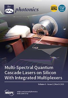
Multi-spectral midwave-infrared (mid-IR) lasers are demonstrated by directly bonding quantum cascade epitaxial gain layers to silicon-on-insulator (SOI) waveguides with arrayed waveguide grating (AWG) multiplexers. Arrays of distributed feedback and distributed Bragg-reflection quantum cascade lasers (QCLs) emitting at 4.7 µm wavelength are coupled to AWGs on the same chip. Low-loss spectral beam combining allows for brightness scaling by coupling the light generated by multiple input QCLs into the fundamental mode of a single output waveguide. Promising results are demonstrated and further improvements are in progress. This device may lead to compact and sensitive chemical detection systems using absorption spectroscopy across a broad spectral range in the mid-IR, as well as a high-brightness multi-spectral source for power scaling. View Paper here.
- Issues are regarded as officially published after their release is announced to the table of contents alert mailing list.
- You may sign up for e-mail alerts to receive table of contents of newly released issues.
- PDF is the official format for papers published in both, html and pdf forms. To view the papers in pdf format, click on the "PDF Full-text" link, and use the free Adobe Reader to open them.
Previous Issue
Next Issue