WO2019126156A1 - Crack-resistant polysiloxane dielectric planarizing compositions, methods and films - Google Patents
Crack-resistant polysiloxane dielectric planarizing compositions, methods and films Download PDFInfo
- Publication number
- WO2019126156A1 WO2019126156A1 PCT/US2018/066217 US2018066217W WO2019126156A1 WO 2019126156 A1 WO2019126156 A1 WO 2019126156A1 US 2018066217 W US2018066217 W US 2018066217W WO 2019126156 A1 WO2019126156 A1 WO 2019126156A1
- Authority
- WO
- WIPO (PCT)
- Prior art keywords
- blocks
- resin
- composition
- poly
- sst
- Prior art date
- Legal status (The legal status is an assumption and is not a legal conclusion. Google has not performed a legal analysis and makes no representation as to the accuracy of the status listed.)
- Ceased
Links
Classifications
-
- C—CHEMISTRY; METALLURGY
- C09—DYES; PAINTS; POLISHES; NATURAL RESINS; ADHESIVES; COMPOSITIONS NOT OTHERWISE PROVIDED FOR; APPLICATIONS OF MATERIALS NOT OTHERWISE PROVIDED FOR
- C09D—COATING COMPOSITIONS, e.g. PAINTS, VARNISHES OR LACQUERS; FILLING PASTES; CHEMICAL PAINT OR INK REMOVERS; INKS; CORRECTING FLUIDS; WOODSTAINS; PASTES OR SOLIDS FOR COLOURING OR PRINTING; USE OF MATERIALS THEREFOR
- C09D183/00—Coating compositions based on macromolecular compounds obtained by reactions forming in the main chain of the macromolecule a linkage containing silicon, with or without sulfur, nitrogen, oxygen, or carbon only; Coating compositions based on derivatives of such polymers
- C09D183/10—Block or graft copolymers containing polysiloxane sequences
-
- C—CHEMISTRY; METALLURGY
- C08—ORGANIC MACROMOLECULAR COMPOUNDS; THEIR PREPARATION OR CHEMICAL WORKING-UP; COMPOSITIONS BASED THEREON
- C08L—COMPOSITIONS OF MACROMOLECULAR COMPOUNDS
- C08L83/00—Compositions of macromolecular compounds obtained by reactions forming in the main chain of the macromolecule a linkage containing silicon with or without sulfur, nitrogen, oxygen or carbon only; Compositions of derivatives of such polymers
- C08L83/04—Polysiloxanes
-
- C—CHEMISTRY; METALLURGY
- C09—DYES; PAINTS; POLISHES; NATURAL RESINS; ADHESIVES; COMPOSITIONS NOT OTHERWISE PROVIDED FOR; APPLICATIONS OF MATERIALS NOT OTHERWISE PROVIDED FOR
- C09D—COATING COMPOSITIONS, e.g. PAINTS, VARNISHES OR LACQUERS; FILLING PASTES; CHEMICAL PAINT OR INK REMOVERS; INKS; CORRECTING FLUIDS; WOODSTAINS; PASTES OR SOLIDS FOR COLOURING OR PRINTING; USE OF MATERIALS THEREFOR
- C09D7/00—Features of coating compositions, not provided for in group C09D5/00; Processes for incorporating ingredients in coating compositions
- C09D7/40—Additives
- C09D7/60—Additives non-macromolecular
- C09D7/63—Additives non-macromolecular organic
-
- C—CHEMISTRY; METALLURGY
- C09—DYES; PAINTS; POLISHES; NATURAL RESINS; ADHESIVES; COMPOSITIONS NOT OTHERWISE PROVIDED FOR; APPLICATIONS OF MATERIALS NOT OTHERWISE PROVIDED FOR
- C09D—COATING COMPOSITIONS, e.g. PAINTS, VARNISHES OR LACQUERS; FILLING PASTES; CHEMICAL PAINT OR INK REMOVERS; INKS; CORRECTING FLUIDS; WOODSTAINS; PASTES OR SOLIDS FOR COLOURING OR PRINTING; USE OF MATERIALS THEREFOR
- C09D7/00—Features of coating compositions, not provided for in group C09D5/00; Processes for incorporating ingredients in coating compositions
- C09D7/80—Processes for incorporating ingredients
-
- C—CHEMISTRY; METALLURGY
- C09—DYES; PAINTS; POLISHES; NATURAL RESINS; ADHESIVES; COMPOSITIONS NOT OTHERWISE PROVIDED FOR; APPLICATIONS OF MATERIALS NOT OTHERWISE PROVIDED FOR
- C09G—POLISHING COMPOSITIONS; SKI WAXES
- C09G1/00—Polishing compositions
- C09G1/06—Other polishing compositions
- C09G1/14—Other polishing compositions based on non-waxy substances
- C09G1/16—Other polishing compositions based on non-waxy substances on natural or synthetic resins
-
- H10P14/6342—
-
- H10P14/6686—
-
- H10P14/6922—
-
- H10P95/06—
-
- C—CHEMISTRY; METALLURGY
- C08—ORGANIC MACROMOLECULAR COMPOUNDS; THEIR PREPARATION OR CHEMICAL WORKING-UP; COMPOSITIONS BASED THEREON
- C08G—MACROMOLECULAR COMPOUNDS OBTAINED OTHERWISE THAN BY REACTIONS ONLY INVOLVING UNSATURATED CARBON-TO-CARBON BONDS
- C08G77/00—Macromolecular compounds obtained by reactions forming a linkage containing silicon with or without sulfur, nitrogen, oxygen or carbon in the main chain of the macromolecule
- C08G77/42—Block-or graft-polymers containing polysiloxane sequences
- C08G77/44—Block-or graft-polymers containing polysiloxane sequences containing only polysiloxane sequences
-
- C—CHEMISTRY; METALLURGY
- C08—ORGANIC MACROMOLECULAR COMPOUNDS; THEIR PREPARATION OR CHEMICAL WORKING-UP; COMPOSITIONS BASED THEREON
- C08K—Use of inorganic or non-macromolecular organic substances as compounding ingredients
- C08K5/00—Use of organic ingredients
- C08K5/16—Nitrogen-containing compounds
- C08K5/17—Amines; Quaternary ammonium compounds
- C08K5/19—Quaternary ammonium compounds
Definitions
- the present invention relates to planarizing materials, and in particular, to planarizing dielectric materials for semiconductor and display manufacturing.
- Improvements in planarizing dielectric materials are desired to provide planarization for advanced semiconductor devices having trenches six microns deep or deeper. It is advantageous that such dielectric materials be crack resistant at such thicknesses, even when exposed to temperatures in excess of 400°C. It is also important for optoelectronic applications that such dielectric materials have a high optical transmittance. The dielectric materials should also be thermally stable when exposed to temperatures exceeding 400°C.
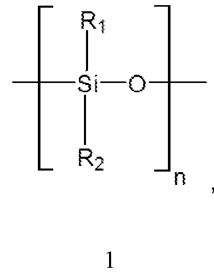
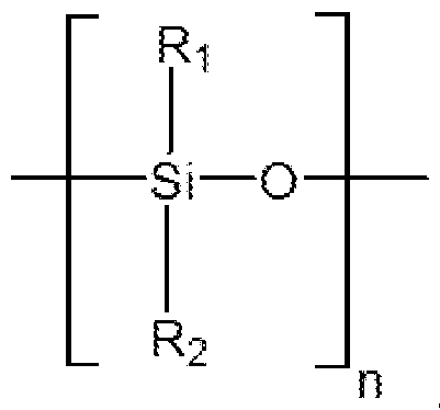
- R-i, R 2 are each independently selected from the group consisting of: an aryl group or an alkyl group, with substituted or unsubstituted carbons.
- compositions for planarizing a semiconductor device includes a catalyst, at least one solvent, and at least one polysiloxane resin including polysilsesquioxane blocks and polydisiloxane blocks.
- the polydisiloxane blocks are according to the general formula:
- Ri, R 2 are each independently selected from the group consisting of: an aryl group or an alkyl group, with substituted or unsubstituted carbons.
- the polydisiloxane blocks include at least one of: poly(diphenylsiloxane) blocks, poly(phenylmethylsiloxane) blocks, and poly(dimethylsiloxane) blocks.
- the polydisiloxane blocks consist of poly (diphenylsiloxane) blocks and poly(phenylmethylsiloxane) blocks.
- the polydisiloxane blocks consist of poly(dimethylsiloxane) blocks.
- the polysilsesquioxane blocks include at least one of: poly(methylsilsesquioxane) blocks and poly(phenylsilsesquioxane) blocks.
- a concentration of the polydisiloxane blocks is from 0.1 mole percent to 50 mole percent of the polysiloxane resin. In some embodiments, a weight average molecular weight of the polydisiloxane blocks in the composition is from 100 Da to 5,000 Da.
- the at least one solvent includes at least one of: ethyl lactate, propylene glycol propyl ether, propylene glycol monomethyl ether acetate, ethanol, isopropyl alcohol, and n-butyl acetate.
- the catalyst includes at least one of: tetramethylammonium acetate, tetramethylammonium hydroxide,
- the composition further includes a surfactant. In some embodiments, the composition further includes a cross-linker. In some embodiments, the at least one polysiloxane resin includes a first polysiloxane resin and a second polysiloxane resin. In some embodiments, the at least one polysiloxane resin is a first polysiloxane resin, and further including a second
- the second polysiloxane resin consisting of a poly(silsesquioxane) resin.
- Various embodiments concern a method for making a planarizing composition.
- the method includes dissolving at least one polysiloxane resin in one or more solvents to form a resin solution and adding a catalyst to the resin solution.
- the at least one polysiloxane resin includes polysilsesquioxane blocks and polydisiloxane blocks.
- the polydisiloxane blocks are according to the general formula:
- Ri, R 2 are each independently selected from the group consisting of: an aryl group or an alkyl group, with substituted or unsubstituted carbons.
- the polydisiloxane blocks include at least one of: poly(diphenylsiloxane) blocks, poly(phenylmethylsiloxane) blocks, and poly(dimethylsiloxane) blocks.
- a concentration of the polydisiloxane blocks is from 0.1 mole percent to 50 mole percent of the polysiloxane resin.
- planarizing film for a semiconductor device.
- the planarizing film includes a catalyst residue and a cured polysiloxane.
- the cured polysiloxane includes polysilsesquioxane blocks and polydisiloxane blocks.
- the polydisiloxane blocks are according to the general formula:
- the polydisiloxane blocks include at least one of: poly(diphenylsiloxane) blocks, poly(phenylmethylsiloxane) blocks, and poly(dimethylsiloxane) blocks.
- a weight average molecular weight of the polydisiloxane blocks is from 100 Da to 5,000 Da.
- a concentration of the polydisiloxane blocks is from 0.1 mole percent to 50 mole percent of the polysiloxane resin.
- FIG. 1 is a schematic cross-section of a portion of a semiconductor device illustrating surface topography to be planarized.
- FIG. 2 is a schematic cross-section of the portion of the semiconductor device of
- FIG. 1 illustrating planarization of the surface topography by a planarization film according to embodiments of this disclosure.
- FIG. 3 is related to Example 15 below and shows the thermal gravimetric analysis results for a planarizing film according to embodiments of this disclosure.
- Embodiments of the disclosure can employ a composition including a
- polysiloxane resin including polysilsesquioxane blocks and polydisiloxane blocks as described below for coating onto a surface of a semiconductor device, such as a microprocessor, a memory device, and a display employing light emitting diodes or other types of displays, to planarize the semiconductor device surface.
- the coating can be applied, for example, by spin-coating or slot coating.
- Planarizing films formed by curing compositions according to embodiments of this disclosure have been found to exhibit excellent crack-resistance at thicknesses greater than 7 microns, even when subjected to temperatures in excess of 400°C.
- Planarizing films formed by curing compositions according to some embodiments of this disclosure have been found to exhibit excellent crack-resistance at thicknesses greater than 10 microns, even when subjected to a temperature of 380°C.
- the planarizing films formed by curing compositions according to embodiments of this disclosure have also been found to exhibit high hardness and high optical transmittance.
- the planarizing films formed by curing compositions according to embodiments of this disclosure have also been found to be thermally stable when exposed to a temperature of 360°C for 24 hours.
- FIG. 1 is a schematic cross-section of a portion of a semiconductor device illustrating surface topography to be planarized.
- FIG. 1 shows a semiconductor device 10 including a substrate 12 and at least one surface feature 14.
- the substrate 12 can include, for example, silicon, silicon dioxide, silicon nitride, aluminum, copper, or any other materials in various layers of various thicknesses and arrangements for the semiconductor device 10 as desired.
- the surface feature 14 can be a trench formed into the substrate 12
- the surface feature 14 can be described as having a width W and a depth D.
- the depth D of the surface feature 14 can be as small as 0.01 microns, 0.1 microns, 0.5 microns, or 1 micron, as large as 3 microns, 5 microns, 10 microns, 100 microns.
- the depth D of the surface feature 14 can range from 0.01 microns to 100 microns, 0.1 microns to 10 microns, 0.5 microns to 5 microns, or 1 micron to 3 microns.
- width W of the surface feature 14 can be as small as 0.01 microns, 0.1 microns, 1 micron, 10 microns, or as great as 50 microns, 100 microns, 500 microns, 1000 microns. In some embodiments, the width W of the surface feature 14 can range from 0.01 microns to 1000 microns, 0.1 microns to 500 microns, 1 micron to 100 microns, or 10 microns to 50 microns.
- FIG. 2 is a schematic cross-section of the portion of the semiconductor device 10 of FIG. 1 illustrating planarization of the surface feature 14 by a planarizing film 16 according to embodiments of this disclosure.
- FIG. 2 shows the semiconductor device 10 after formation of the planarizing film 16 from a composition including a polysiloxane resin according to embodiments of this disclosure.
- the planarizing film 16 can fill the surface feature 14 to provide a substantially planar surface 18 upon which subsequent devices layers (not shown) may be formed.
- the planarizing film 16 can have a thickness T over a portion of the semiconductor device 10 that is greater than 6 microns.
- the planarizing film 16 can have a thickness T over a portion of the semiconductor device 10 that is greater than 10 microns.
- FIGS. 1 and 2 illustrate one example in which the planarizing film 16 according to embodiments of the disclosure may be formed. It is understood that the planarizing film 16 according to embodiments of the disclosure may be formed on many other topographies involving different arrangements of conductive, non-conductive, and semi-conductive materials. For ease of illustration, only one surface feature 14 is shown in FIGS. 1 and 2. However it is understood that embodiments can include a plurality of surface features 14.
- the planarizing film 16 can be formed by coating at least a portion of the semiconductor device 10 by, for example, spin coating or slot coating a composition including at least one solvent, a catalyst, and a polysiloxane resin as described below.
- the composition can further include a surfactant.
- the composition can further include a cross-linker.
- the composition consists essentially of a composition including at least one solvent, a catalyst, a surfactant, and at least one polysiloxane resin as described below.
- the composition consists essentially of a composition including at least one solvent, a catalyst, a surfactant, a cross-linker, and at least one polysiloxane resin as described below.
- the polysiloxane resin can include polysilsesquioxane blocks and polydisiloxane blocks.
- the polysilsesquioxane blocks can include any type of polysilsesquioxane with the formula [RSi0 3/2 ] n , wherein R is a hydrogen, an alkyl group, an aryl group, or an alkoxyl group.
- the polysilsesquioxane blocks can include poly(methylsilsesquioxane) blocks, poly(phenylsilsesquioxane) blocks,
- polydisiloxane blocks are according to the formula:
- the polydisiloxane blocks can include poly(diphenylsiloxane) blocks in which Ri and R 2 are each phenyl groups.
- the polydisiloxane blocks can include poly(dimethylsiloxane) blocks in which Ri and R 2 are each methyl groups.
- the polydisiloxane blocks can include poly(phenylmethylsiloxane) blocks in which Ri is a phenyl group and R 2 is a methyl group.
- the polysiloxane resin can include a single type of polydisiloxane block.
- the polydisiloxane blocks consist of poly(dimethylsiloxane) blocks, such as in SST-3PM2 dimethylsiloxane copolymer resin available from Gelest Inc., Morrisville, Pennsylvania.
- the polysiloxane resin can include more than one type of polydisiloxane block. For example, in some
- the polydisiloxane blocks can include any combination of poly(diphenylsiloxane) blocks, poly(dimethylsiloxane) blocks, or poly(phenylmethylsiloxane) blocks.
- the polydisiloxane blocks can consist of poly(diphenylsiloxane) blocks and poly(phenylmethylsiloxane) blocks, such as in SST-3PM4 tetrapolymer resin available from Gelest Inc., Morrisville, Pennsylvania.
- the polydisiloxane blocks can consist of poly(diphenylsiloxane) blocks, poly(dimethylsiloxane) blocks, and
- the polydisiloxane blocks in the polysiloxane resin can have a weight average molecular weight (Mw).
- weight average molecular weight (Mw) of the polydisiloxane blocks in the composition is as low as 100 Da, 200 Da, 500 Da, 800 Da, 1,000 Da, or 1,200 Da or as high as 1,600 Da, 2,100 Da, 2,600 Da, 3,400 Da, 4,300 Da, or 5,000 Da, or within any range defined by any two of the preceding values.
- Mw weight average molecular weight
- the Mw of the polydisiloxane blocks in the composition ranges from 100 Da to 5,000 Da, 200 Da to 4,300 Da, 1,000 Da to 2,100 Da, 1,200 DA to 4,300 Da, or 1,200 Da to 1,600 Da. In some embodiments, the Mw of the polydisiloxane blocks in the composition is about 1,300 Da. The Mw can be measured by gel permeation chromatography, as is known in the art.
- a concentration of the polydisiloxane blocks in the polysiloxane resin can be as low as 0.1 mole percent (mol %), 1 mol %, 10 mol %, or 20 mol % or as high as 25 mol %, 30 mol %, 35 mol %, 40 mol %, or 50 mol % of the polysiloxane resin, or within any range defined by any two of the preceding values, for example, in some embodiments, the concentration of the polydisiloxane blocks in the composition can range from 0.1 mol % to 50 mol %, 1 mol % to 45 mol %, 10 mol % to 40 mol %, or 20 mol % to 30 mol % of the polysiloxane resin.
- the at least one polysiloxane resin can consist of any one of the polysilicon resins described above.
- the at least one polysiloxane resin can include a first polysiloxane resin and a second polysiloxane resin that is different from the first polysiloxane resin.
- the first polysiloxane resin and the second polysiloxane resin are each one of the polysiloxane resins described above.
- the first polysiloxane resin can be one of the polysiloxane resins described above
- the second polysiloxane resin can be a poly(silsesquioxane) resin that is not one of the polysiloxane resins described above, for example, poly(phenyl-methyl silsesquioxane) resin.
- the at least one solvent can include a single solvent, such as a glycol ether, a glycol ether acetate, n-butyl acetate, a ketone, or an alcohol.
- Glycol ethers can include, for example, propylene glycol propyl ether or propylene glycol methyl ether.
- Glycol ether acetates can include, for example, propylene glycol methyl ether acetate (PGMEA), 2-ethoxyethyl acetate, or 2-methoxyethyl acetate.
- Ketones can include, for example, acetone or diethyl ketone.
- Alcohols can include, for example, isopropyl alcohol, butanol, or ethanol. In other
- the at least one solvent includes a mixture two or more of the foregoing solvents.
- the catalyst can include, for example, tetramethylammonium acetate (TMAA), tetramethylammonium hydroxide (TMAH), tetrabutylammonium acetate (TBAA),
- TMAA tetramethylammonium acetate
- TMAH tetramethylammonium hydroxide
- TBAA tetrabutylammonium acetate
- cetyltrimethylammonium acetate CAA
- TMAN tetramethylammonium nitrate
- Such catalysts can be activated by heat after the composition is applied to the semiconductor device 10 to cause polymerization and cross-linking of the composition to form the planarizing film 16.
- the composition can further include a surfactant. It has been found that a surfactant can further reduce striations, which may be particularly useful when the composition is spin-coated onto larger diameter semiconductor device wafers or display substrates.
- the surfactant can be a polyether-modified
- polydimethylsiloxane surfactant such as BYK®-306 or BYK®-307 available from BYK-Chemie, Wesel, Germany.
- the concentration of the surfactant in the composition can be as low as 0.01 wt. %, 0.1 wt. %, 0.4 wt. %, 0.6 wt. %, or 0.8 wt. %, or as high as 1 wt. %, 5 wt. %, 10 wt. %, 15 wt. %, or 20 wt. % of the total weight of the composition, or within any range defined by any two of the preceding values, for example, in some embodiments, the concentration of the surfactant in the composition can range from 0.01 wt. % to 20 wt. %, 0.1 wt. % to 15 wt. %, 0.4 wt. % to 10 wt. %, 0.6 wt. % to 5 wt. %, or 0.8 wt. % to 1 wt. % of the total weight of the composition.
- the composition can further include an organic acid which can volatilize or decompose at high temperatures to help stabilize the composition.
- the organic acid can include trifluoroacetic acid, p-toluenesulfonic acid, citric acid, formic acid, or acetic acid, or any combinations thereof.
- the concentration of the organic acid can include as little as 0.01 wt. %, 0.1 wt. %, 0.2 wt. %, or 0.4 wt. %, or as much as 0.5 wt. %, 0.6 wt. %, 0.8 wt. %, or 1 wt.
- the concentration of the organic acid in the composition can range from 0.01 wt. % to 1 wt. %, 0.1 wt. % to 0.8 wt. %, 0.3 wt. % to 0.6 wt. %, or 0.4 wt. % to 0.5 wt. % of the total weight of the composition.
- the composition can further include a cross-linker.
- Cross- linkers form bonds in the polysiloxane resin. Without wishing to be bound by any theory, it is believed that the bonds provided by the cross-linker provide additional structure and strength to the planarizing film 16, providing additional crack resistance.
- the cross- linker can include bis-(trimethoxysilylpropyl) amine, 1,3 bis(triethoxysilyl) benzene, 1,4 bis(triethoxysilyl) benzene, 2,6-bis(triethoxysilyl)-naphthalene, 9, 10-bis(triethoxysilyl)- anthracene, l,6-bis(trimethoxysilyl)-pyrene, bis(triethoxysilyl) methane, l,2-bis(triethoxysily) ethane, or 1 -(triethoxysilyl)-2-(diethoxymethylsilyl) ethane, or any combination thereof.
- a method for making a planarizing composition in accordance with embodiments of this disclosure can include providing at least one polysiloxane resin as described above and dissolving the polysiloxane resin in the one or more solvents to form a resin solution.
- Dissolving the polysiloxane resin can be encouraged by mixing the polysiloxane resin into the one or more solvents for one to four hours.
- a catalyst as described above can be added to the resin solution.
- a surfactant as described above can also be added to the resin solution.
- the resin solution can be stirred for several more hours, for example, three hours to form the composition.
- the composition may then be filtered through a 0.1 micron filter.
- a planarizing composition in accordance with embodiments of this disclosure can be applied to the semiconductor device 10 (FIG. 1) by, for example spin coating.
- the coated semiconductor device 10 can then be bake at a temperature ranging from about l60°C to about l80°C to drive off substantially all of the at least one solvent and form an uncured film.
- a second coating of the planarizing composition can be applied on the uncured film and the coated semiconductor device 10 baked again at a temperature ranging from about l60°C to about l80°C to drive off substantially all of the at least one solvent and form a second layer of uncured film.
- the coating and backing processes can be completed until a desired thickness of uncured film is realized, after which the catalyst can be activated by heat to cure the film by polymerizing and cross-linking the polysiloxane resin to form the planarizing film 16. Residues of the catalyst can remain after curing.
- the planarizing film 16 can be cured at a temperature as low as 250°C, 260°C, 280°C, 300°C, or 350°C, or as high as 400°C, 4lO°C, 420°C, 430°C, 440°C, or 450°C, or at any temperature between any two of the preceding temperatures.
- the planarizing film 16 can be cured a temperature ranging from 250°C to 450°C, 260°C to 440°C, 280°C to 430°C, 300°C to 420°C, or 350°C to 4lO°C.
- the planarizing film 16 can further include a surfactant residue, according to any of the embodiments described above, including a residue of a polyether-modified polydimethylsiloxane surfactant, such a BYK®-307.
- GR150F resin obtained from Techneglas of Perrysburg, Ohio was added to 55.0 g of PGMEA and stirred for 1 hour at room temperature to form a GR150F resin solution.
- GR150 is a poly(silsesquioxane) resin including equimolar amounts of poly(methylsilsesquioxane) blocks and poly(phenylsilsesquioxane) blocks with about 0.3 mole % of poly(dimethylsiloxane) blocks.
- % surfactant solution and 0.8 g of the TMAN catalyst solution were added to 100 g of the GR150F solution and stirred for 3 hours at room temperature to form a planarizing composition.
- the planarizing composition was filtered through a 0.1 micron filter.
- the filtered planarizing composition was coated on a four-inch silicon wafer by spin coating at 1,500 revolutions per minute (RPM).
- the wafer with the cast film was baked on a series of two hot plates in air ambient for 60 seconds each, a first hot plate having a surface temperature of l60°C and a second hot plate having a surface temperature of 180°C, to evaporate the solvents.
- the wafer with the baked coating was cured in a nitrogen ambient at 350°C for 1 hour.
- the cured coating was inspected for cracking by optical microscopy and scanning electron microscopy. Severe cracking of the cured coating was observed.
- Example 2 Comparative Example - Polv(silsesquioxane) Resin SST-3PM1 [0039] In a 200 ml flask, 45.0 g of SST-3PM1 resin obtained from Gelest Inc.,
- SST-3PM1 is a polysilsesquioxane resin including 90 mole % poly(phenylsilsesquioxane) blocks and 10 mole %
- poly(methylsilsesquioxane) blocks In another 200 ml flask, 1.25 g of the 10 wt. % surfactant solution prepared as described above and 0.8 g of the TMAN catalyst solution prepared as described above were added to 100 g of the SST-3PM1 resin solution and stirred for 3 hours at room temperature to form a planarizing composition. The planarizing composition was filtered through a 0.1 micron filter.
- the filtered planarizing composition was coated on a four-inch silicon wafer by spin coating at 1,500 RPM.
- the wafer with the cast film was baked on a series of two hot plates in air ambient for 60 seconds each, a first hot plate having a surface temperature of l60°C and a second hot plate having a surface temperature of l80°C, to evaporate the solvents.
- a thickness of the baked coating was measured and found to be 28,439 A.
- the wafer with the baked coating was cured in a nitrogen ambient at 350°C for 1 hour. The cured coating was inspected for cracking by optical microscopy and scanning electron microscopy. No cracking of the cured coating was observed.
- SST-3PM2 is a dimethylsiloxane copolymer resin including 70 mole % poly(phenylsilsesquioxane) blocks and 30 mole %
- poly(dimethylsiloxane) copolymer blocks In another 200 ml flask, 1.25 g of the 10 wt. % surfactant solution prepared as described above and 0.8 g of the TMAN catalyst solution prepared as described above were added to 100 g of the SST-3PM2 resin solution and stirred for 3 hours at room temperature to form a planarizing composition. The planarizing composition was filtered through a 0.1 micron filter.
- the filtered planarizing composition was coated on a four-inch silicon wafer by spin coating at 1,500 RPM.
- the wafer with the cast film was baked on a series of two hot plates in air ambient for 60 seconds each, a first hot plate having a surface temperature of l60°C and a second hot plate having a surface temperature of l80°C, to evaporate the solvents.
- the wafer with the baked coating was cured in a nitrogen ambient at 350°C for 1 hour.
- the cured coating was inspected for cracking by optical microscopy and scanning electron microscopy. No cracking of the cured coating was observed.
- SST-3PM4 is a dimethylsiloxane copolymer resin including 45 mole % poly(methylsilsesquioxane) blocks, 40 mole %
- poly(phenylsilsesquioxane) blocks 15 mole % poly(phenylmethylsiloxane) blocks, and 10 mole % poly(diphenylsiloxane) blocks.
- 1.25 g of the 10 wt. % surfactant solution prepared as described above and 0.8 g of the TMAN catalyst solution prepared as described above were added to 100 g of the SST-3PM4 resin solution and stirred for 3 hours at room temperature to form a planarizing composition.
- the planarizing composition was filtered through a 0.1 micron filter.
- the filtered planarizing composition was coated on a four-inch silicon wafer by spin coating at 1,500 RPM.
- the wafer with the cast film was baked on a series of two hot plates in air ambient for 60 seconds each, a first hot plate having a surface temperature of l60°C and a second hot plate having a surface temperature of l80°C, to evaporate the solvents.
- a thickness of the baked coating was measured and found to be 32,556 A.
- the wafer with the baked coating was cured in a nitrogen ambient at 350°C for 1 hour. The cured coating was inspected for cracking by optical microscopy and scanning electron microscopy. No cracking of the cured coating was observed.
- % surfactant solution prepared as described above and 0.8 g of the TMAN catalyst solution prepared as described above were added to 95 g of the GR150F resin solution and 5 g of the SST-3PM2 resin solution and stirred for 3 hours at room temperature to form a planarizing composition.
- the planarizing composition was filtered through a 0.1 micron filter.
- the filtered planarizing composition was coated on a four-inch silicon wafer by spin coating at 1,500 RPM.
- the wafer with the cast film was baked on a series of two hot plates in air ambient for 60 seconds each, a first hot plate having a surface temperature of l60°C and a second hot plate having a surface temperature of l80°C, to evaporate the solvents.
- a thickness of the baked coating was measured and found to be 32,425 A.
- the wafer with the baked coating was cured in a nitrogen ambient at 350°C for 1 hour.
- the cured coating was inspected for cracking by optical microscopy and scanning electron microscopy. Cracking of the cured coating was observed. The cracking was to a lesser degree than the cracking observed in Comparative Example 1.
- % surfactant solution prepared as described above and 0.8 g of the TMAN catalyst solution prepared as described above were added to 75 g of the GR150F resin solution and 25 g of the SST-3PM2 resin solution and stirred for 3 hours at room temperature to form a planarizing composition.
- the planarizing composition was filtered through a 0.1 micron filter.
- the filtered planarizing composition was coated on a four-inch silicon wafer by spin coating at 1,500 RPM.
- the wafer with the cast film was baked on a series of two hot plates in air ambient for 60 seconds each, a first hot plate having a surface temperature of l60°C and a second hot plate having a surface temperature of l80°C, to evaporate the solvents.
- a thickness of the baked coating was measured and found to be 32,790 A.
- the wafer with the baked coating was cured in a nitrogen ambient at 350°C for 1 hour.
- the cured coating was inspected for cracking by optical microscopy and scanning electron microscopy. Cracking of the cured coating was observed. The cracking was to a lesser degree than the cracking observed in Comparative Example 1.
- % surfactant solution prepared as described above and 0.8 g of the TMAN catalyst solution prepared as described above were added to 100 g of the SST-3PM1 resin solution and 1 g of the SST-3PM2 resin solution and stirred for 3 hours at room temperature to form a planarizing composition.
- the planarizing composition was filtered through a 0.1 micron filter.
- the filtered planarizing composition was coated on a four-inch silicon wafer by spin coating at 1,500 RPM.
- the wafer with the cast film was baked on a series of two hot plates in air ambient for 60 seconds each, a first hot plate having a surface temperature of l60°C and a second hot plate having a surface temperature of l80°C, to evaporate the solvents.
- a thickness of the baked coating was measured and found to be 12,942 A.
- the wafer with the baked coating was cured in a nitrogen ambient at 350°C for 1 hour. The cured coating was inspected for cracking by optical microscopy and scanning electron microscopy. No cracking of the cured coating was observed.
- % surfactant solution prepared as described above and 0.32 g of the TMAN catalyst solution prepared as described above were added to 10 g of the SST-3PM1 resin solution and 30 g of the SST-3PM4 resin solution and stirred for 3 hours at room temperature to form a planarizing composition.
- the planarizing composition was filtered through a 0.1 micron filter.
- the filtered planarizing composition was coated on two, four-inch silicon wafers by spin coating at 1,500 RPM.
- the wafers with the cast film were baked on a series of two hot plates in air ambient for 60 seconds each, a first hot plate having a surface temperature of l60°C and a second hot plate having a surface temperature of 180°C, to evaporate the solvents.
- a thickness of the baked coating was measured for each wafer and found to be 31,873 A and 31,915 A.
- One of the wafers was cured in a nitrogen ambient at 4lO°C for 30 minutes and the other cured in a nitrogen ambient at 450°C for 30 minutes.
- the cured coatings were inspected for cracking by optical microscopy and scanning electron microscopy. No cracking of the cured coating on either wafer was observed.
- % surfactant solution prepared as described above and 0.32 g of the TMAN catalyst solution prepared as described above were added to 20 g of the SST-3PM1 resin solution and 20 g of the SST-3PM4 resin solution and stirred for 3 hours at room temperature to form a planarizing composition.
- the planarizing composition was filtered through a 0.1 micron filter. [0054]
- the filtered planarizing composition was coated on two, four-inch silicon wafers by spin coating at 1,500 RPM.
- the wafers with the cast film were baked on a series of two hot plates in air ambient for 60 seconds each, a first hot plate having a surface temperature of l60°C and a second hot plate having a surface temperature of 180°C, to evaporate the solvents.
- a thickness of the baked coating was measured for each wafer and found to be 31,897 A and 31,896 A.
- One of the wafers was cured in a nitrogen ambient at 4lO°C for 30 minutes and the other cured in a nitrogen ambient at 450°C for 30 minutes.
- the cured coatings were inspected for cracking by optical microscopy and scanning electron microscopy. No cracking of the cured coating on either wafer was observed.
- % surfactant solution prepared as described above and 0.32 g of the TMAN catalyst solution prepared as described above were added to 30 g of the SST-3PM1 resin solution and 10 g of the SST-3PM4 resin solution and stirred for 3 hours at room temperature to form a planarizing composition.
- the planarizing composition was filtered through a 0.1 micron filter.
- the filtered planarizing composition was coated on two, four-inch silicon wafers by spin coating at 1,500 RPM.
- the wafers with the cast film were baked on a series of two hot plates in air ambient for 60 seconds each, a first hot plate having a surface temperature of l60°C and a second hot plate having a surface temperature of 180°C, to evaporate the solvents.
- a thickness of the baked coating was measured for each wafer and found to be 31,684 A and 31,722 A.
- One of the wafers was cured in a nitrogen ambient at 4lO°C for 30 minutes and the other cured in a nitrogen ambient at 450°C for 30 minutes.
- the cured coatings were inspected for cracking by optical microscopy and scanning electron microscopy. No cracking of the cured coating on either wafer was observed.
- % surfactant solution prepared as described above and 0.8 g of the TMAN catalyst solution prepared as described above were added to 100 g of the SST-3PM4 resin solution and 1 g of the SST-3PM2 resin solution and stirred for 3 hours at room temperature to form a planarizing composition.
- the planarizing composition was filtered through a 0.1 micron filter.
- the filtered planarizing composition was coated on a four-inch silicon wafer by spin coating at 1,500 RPM.
- the wafer with the cast film was baked on a series of two hot plates in air ambient for 60 seconds each, a first hot plate having a surface temperature of l60°C and a second hot plate having a surface temperature of l80°C, to evaporate the solvents.
- a thickness of the baked coating was measured and found to be 14,231 A.
- the wafer with the baked coating was cured in a nitrogen ambient at 350°C for 1 hour. The cured coating was inspected for cracking by optical microscopy and scanning electron microscopy. No cracking of the cured coating was observed.
- % surfactant solution prepared as described above and 0.8 g of the TMAN catalyst solution prepared as described above were added to 100 g of the SST-3PM4 resin solution and 1 g of the SST-3PM2 resin solution and stirred for 3 hours at room temperature to form a planarizing composition.
- the planarizing composition was filtered through a 0.1 micron filter.
- the filtered planarizing composition was coated onto five, four-inch silicon wafers by spin coating, two at 1,000 RPM, two at 1,500 RPM, and one at 2,400 RPM.
- the wafers with the cast films were baked on a series of two hot plates in air ambient for 60 seconds each, a first hot plate having a surface temperature of l60°C and a second hot plate having a surface temperature of 180°C, to evaporate the solvents.
- One of the two wafers coated at 1,000 RPM, one of the two wafers coated at 1,500 RPM, and the wafer coated at 2,400 RPM each received a second coating, each spun at same speed as for their first coating and baked again on the hot plates as described above.
- a thickness of the baked coating was measured for several of the wafers and found to be 43,458 A for the single coating at 1,000 RPM, 93,494 A for the double coating at 1,000 RPM, 32,440 A for the single coating at 1,500 RPM, and 54,973 A for the double coating at 2,400 RPM.
- the five wafers with the baked coatings were cured in a nitrogen ambient at 4lO°C for 30 minutes.
- the cured coatings were inspected for cracking by optical microscopy and scanning electron microscopy. No cracking of the cured coatings was observed on the wafers with coating thicknesses up to 54,973 A. Cracking was observed only on the wafer having a coating thickness of 93,494 A.
- tetrabutylammonium nitrate (TBAA) catalyst was added to 24.5 g of deionized water and stirred for 1 hour at room temperature to prepare a 2 wt. % TBAA catalyst solution.
- TBAA tetrabutylammonium nitrate
- 45.0 g of SST-3PM4 resin was added to 55.0 g of PGMEA and stirred for 1 hour at room temperature to form an SST-3PM4 resin solution.
- 45.0 g of SST-3PM2 resin was added to 55.0 g of PGMEA and stirred for 1 hour at room temperature to form an SST-3PM2 resin solution.
- the filtered planarizing composition was coated onto three, four-inch silicon wafers by spin coating, one at 600 RPM, one at 1,000 RPM, and one at 1,500 RPM.
- the wafers with the cast films were baked on a series of two hot plates in air ambient for 60 seconds each, a first hot plate having a surface temperature of l60°C and a second hot plate having a surface temperature of l80°C, to evaporate the solvents.
- a thickness of the baked coating was measured for the wafers and found to be 37,020 A for the single coating at 1,500 RPM and 50,012 A for the single coating at 1 ,000 RPM.
- the thickness for the single coating at 600 RPM could not be measured because the spin speed is too low to produce a uniform coating.
- the three wafers with the baked coatings were cured in a nitrogen ambient at 4lO°C for 30 minutes.
- the cured coatings were inspected for cracking by optical microscopy and scanning electron microscopy. No cracking of the cured coatings was observed on the wafers coated at 1,500 RPM. Cracking was observed on the wafer coated at 1,000 RPM.
- % surfactant solution prepared as described above, 0.8 g of the TMAN catalyst solution prepared as described above, and 0.45 g of a cross-linker were added to 100 g of the SST-3PM4 resin solution and 1 g of the SST-3PM2 resin solution and stirred for 3 hours at room temperature to form a planarizing composition.
- the cross-linker was Silquest® A-l 170 (bis- (trimethoxysilylpropyl) amine) obtained from Momentive Performance Materials, Waterford, New York.
- the planarizing composition was filtered through a 0.1 micron filter.
- the filtered planarizing composition was coated onto twelve, four-inch silicon wafers by spin coating, three at 1,000 RPM, three at 1,300 RPM, three at 1,800 RPM, and three at 2,400 RPM.
- the wafers with the cast films were baked on a series of two hot plates in air ambient for 60 seconds each, a first hot plate having a surface temperature of l60°C and a second hot plate having a surface temperature of l80°C, to evaporate the solvents.
- Each of the wafers received a second coating, each spun at same speed as for their first coating and baked again on the hot plates as described above. A thickness of the baked coating was measured for each of the wafers.
- the twelve wafers were cured in a nitrogen ambient for 30 minutes.
- % surfactant solution prepared as described above 0.8 g of the TMAN catalyst solution prepared as described above, and 0.45 g of (bis-(trimethoxysilylpropyl) amine cross-linker described above were added to 100 g of the SST-3PM4 resin solution and 1 g of the SST-3PM2 resin solution and stirred for 3 hours at room temperature to form a planarizing composition.
- the planarizing composition was filtered through a 0.1 micron filter.
- the filtered planarizing composition was coated on a four-inch silicon wafer by spin coating at 1,500 RPM.
- the wafer with the cast film was baked on a series of two hot plates in air ambient for 60 seconds each, a first hot plate having a surface temperature of l60°C and a second hot plate having a surface temperature of 180°C, to evaporate the solvents.
- the wafer with the baked coating was cured in a nitrogen ambient at 4lO°C for 30 minutes.
- the cured coating was collected from the wafer and subjected to TGA analysis on a Discovery TGA System. The sample was heated in N 2 from room temperature (25°C) to about 360°C and held for 24 hours. The results are presented in FIG. 3.
- FIG. 3 The results are presented in FIG. 3.
- FIG. 3 illustrates a temperature profile 20 of the TGA (in reference to the right-hand axis) and a weight 22 of the coating as a percentage of the initial coating weight (in reference to the left-hand axis). As shown in FIG. 3, the coating is thermally stable, losing less than 1% weight after heating at 360°C for 24 hours.
- PGMEA PGMEA
- stirred for 1 hour at room temperature to form a diluted planarizing composition.
- the diluted planarizing composition was filtered through a 0.1 micron filter.
- the filtered diluted planarizing composition was coated on an 8-inch silicon wafer and on a 2-inch by 2-inch transparent glass substrate by spin coating at 1,500 RPM.
- the silicon wafer and glass substrate with the cast films were baked on a series of two hot plates in air ambient for 60 seconds each, a first hot plate having a surface temperature of l60°C and a second hot plate having a surface temperature of l80°C, to evaporate the solvents.
- the wafers with the baked coatings were cured in an air ambient at 250°C for 60 minutes.
- UV-Vis spectrophotometer An optical transmittance of 92.1 % was measured for the glass substrate with no coating, and an optical transmittance of 91.6% was measured for the cured coating on the glass substrate, showing high transparency for the cured coating.
- the 8-inch silicon wafer with the cured coating was measured for nanohardness and reduced elastic modulus analysis by a nanoindentation test on a Hysitron® Nanomechanical Test System. A high nanohardness of 145.1 Mpa and a reduced elastic modulus of 3.49 GPa were measured for the cured coating on the silicon wafer.
Landscapes
- Chemical & Material Sciences (AREA)
- Organic Chemistry (AREA)
- Engineering & Computer Science (AREA)
- Life Sciences & Earth Sciences (AREA)
- Materials Engineering (AREA)
- Wood Science & Technology (AREA)
- Chemical Kinetics & Catalysis (AREA)
- Health & Medical Sciences (AREA)
- Medicinal Chemistry (AREA)
- Polymers & Plastics (AREA)
- Compositions Of Macromolecular Compounds (AREA)
- Silicon Polymers (AREA)
- Physics & Mathematics (AREA)
- Condensed Matter Physics & Semiconductors (AREA)
- General Physics & Mathematics (AREA)
- Manufacturing & Machinery (AREA)
- Computer Hardware Design (AREA)
- Microelectronics & Electronic Packaging (AREA)
- Power Engineering (AREA)
- Formation Of Insulating Films (AREA)
- Manufacture Of Macromolecular Shaped Articles (AREA)
- Inorganic Insulating Materials (AREA)
- Paints Or Removers (AREA)
Abstract
Description


Claims


Priority Applications (5)
| Application Number | Priority Date | Filing Date | Title |
|---|---|---|---|
| CN201880087090.9A CN111615542A (en) | 2017-12-19 | 2018-12-18 | Crack-resistant polysiloxane dielectric planarization compositions, methods and films |
| JP2020533781A JP2021507052A (en) | 2017-12-19 | 2018-12-18 | Crack-resistant polysiloxane dielectric flattening composition, method, and film |
| EP18891231.5A EP3728500A4 (en) | 2017-12-19 | 2018-12-18 | CRACK RESISTANT POLYSILOXANE-BASED DIELECTRIC PLANARIZATION PROCESSES, FILMS AND COMPOSITIONS |
| KR1020207020034A KR102723969B1 (en) | 2017-12-19 | 2018-12-18 | Crack-resistant polysiloxane dielectric planarization compositions, methods and films |
| JP2023177251A JP7645959B2 (en) | 2017-12-19 | 2023-10-13 | Crack-resistant polysiloxane dielectric planarization compositions, methods, and films |
Applications Claiming Priority (4)
| Application Number | Priority Date | Filing Date | Title |
|---|---|---|---|
| US201762607461P | 2017-12-19 | 2017-12-19 | |
| US62/607,461 | 2017-12-19 | ||
| US16/210,160 | 2018-12-05 | ||
| US16/210,160 US11015082B2 (en) | 2017-12-19 | 2018-12-05 | Crack-resistant polysiloxane dielectric planarizing compositions, methods and films |
Publications (1)
| Publication Number | Publication Date |
|---|---|
| WO2019126156A1 true WO2019126156A1 (en) | 2019-06-27 |
Family
ID=66814158
Family Applications (1)
| Application Number | Title | Priority Date | Filing Date |
|---|---|---|---|
| PCT/US2018/066217 Ceased WO2019126156A1 (en) | 2017-12-19 | 2018-12-18 | Crack-resistant polysiloxane dielectric planarizing compositions, methods and films |
Country Status (7)
| Country | Link |
|---|---|
| US (1) | US11015082B2 (en) |
| EP (1) | EP3728500A4 (en) |
| JP (2) | JP2021507052A (en) |
| KR (1) | KR102723969B1 (en) |
| CN (1) | CN111615542A (en) |
| TW (1) | TWI798312B (en) |
| WO (1) | WO2019126156A1 (en) |
Families Citing this family (1)
| Publication number | Priority date | Publication date | Assignee | Title |
|---|---|---|---|---|
| US20240400858A1 (en) * | 2023-05-23 | 2024-12-05 | Honeywell International Inc. | High crack threshold planarizing coatings and processes to fill wide and deep trenches for silicone wafers |
Citations (5)
| Publication number | Priority date | Publication date | Assignee | Title |
|---|---|---|---|---|
| US20090225640A1 (en) * | 2006-07-21 | 2009-09-10 | Kaneka Corporation | Polysiloxane composition, molded body obtained from the same, and optodevice member |
| US20110171447A1 (en) * | 2004-08-03 | 2011-07-14 | Ahila Krishnamoorthy | Compositions, layers and films for optoelectronic devices, methods of production and uses thereof |
| US20130210202A1 (en) * | 2012-02-14 | 2013-08-15 | Samsung Display Co., Ltd. | Method of planarizing substrate and method of manufacturing thin film transistor using the same |
| WO2016167892A1 (en) * | 2015-04-13 | 2016-10-20 | Honeywell International Inc. | Polysiloxane formulations and coatings for optoelectronic applications |
| WO2017145808A1 (en) * | 2016-02-24 | 2017-08-31 | 日産化学工業株式会社 | Planarization method for semiconductor substrates using silicon-containing composition |
Family Cites Families (45)
| Publication number | Priority date | Publication date | Assignee | Title |
|---|---|---|---|---|
| US5286572A (en) * | 1988-11-28 | 1994-02-15 | International Business Machines Corporation | Planarizing ladder-type silsequioxane polymer insulation layer |
| US5152834A (en) * | 1990-09-14 | 1992-10-06 | Ncr Corporation | Spin-on glass composition |
| JPH04185641A (en) * | 1990-11-20 | 1992-07-02 | Fujitsu Ltd | Production of heat-resistant resin composition and insulation film |
| US5412053A (en) * | 1993-08-12 | 1995-05-02 | The University Of Dayton | Polymers containing alternating silsesquioxane and bridging group segments and process for their preparation |
| JP3078326B2 (en) * | 1994-03-11 | 2000-08-21 | 川崎製鉄株式会社 | Coating liquid for forming insulating film, method for manufacturing the same, method for forming insulating film for semiconductor device, and method for manufacturing semiconductor device using the same |
| JP2893243B2 (en) * | 1994-11-25 | 1999-05-17 | 昭和電工株式会社 | Composition for semiconductor insulating film and planarizing film, and method for forming the film |
| JP3488965B2 (en) * | 1996-05-21 | 2004-01-19 | 日本山村硝子株式会社 | Method for producing independent membrane by sol-gel method |
| US5962067A (en) | 1997-09-09 | 1999-10-05 | Lucent Technologies Inc. | Method for coating an article with a ladder siloxane polymer and coated article |
| JP2000302869A (en) * | 1999-04-23 | 2000-10-31 | Jsr Corp | Method for producing film-forming composition |
| US7888435B2 (en) | 1999-08-04 | 2011-02-15 | Hybrid Plastics, Inc. | Process for continuous production of olefin polyhedral oligomeric silsesquioxane cages |
| US6410151B1 (en) * | 1999-09-29 | 2002-06-25 | Jsr Corporation | Composition for film formation, method of film formation, and insulating film |
| EP1160848B1 (en) * | 2000-05-22 | 2011-10-05 | JSR Corporation | Composition for silica-based film formation |
| US20040047988A1 (en) * | 2000-11-17 | 2004-03-11 | Jin-Kyu Lee | Poly(methylsilsesquioxane) copolymers and preparation method thereof |
| JP2002285086A (en) * | 2001-03-26 | 2002-10-03 | Jsr Corp | Film forming composition, film forming method and silica-based film |
| JP3631236B2 (en) * | 2002-07-12 | 2005-03-23 | 東京応化工業株式会社 | Method for producing silica-based organic coating |
| KR100507967B1 (en) * | 2003-07-01 | 2005-08-10 | 삼성전자주식회사 | Siloxane-based Resin and Semiconductive Interlayer Insulating Film Using the Same |
| KR20050040275A (en) * | 2003-10-28 | 2005-05-03 | 삼성전자주식회사 | Composition for forming dielectric film and method for forming dielectric film or pattern using the same |
| GB0401202D0 (en) | 2004-01-20 | 2004-02-25 | Ucl Biomedica Plc | Polymer for use in conduits and medical devices |
| JP4834972B2 (en) * | 2004-09-17 | 2011-12-14 | 東レ株式会社 | Coating composition and display device using the same |
| KR20060068348A (en) * | 2004-12-16 | 2006-06-21 | 삼성코닝 주식회사 | Siloxane-based polymer and insulating film production method using the polymer |
| KR101119141B1 (en) * | 2005-01-20 | 2012-03-19 | 삼성코닝정밀소재 주식회사 | Composition for forming low dielectric film comprising polymeric nanoparticles and method for preparing low dielectric thin film using the same |
| US7373060B2 (en) * | 2005-02-28 | 2008-05-13 | Chisso Corporation | Optical waveguide using polymer composed of silsesquioxane derivative |
| US7435989B2 (en) * | 2005-09-06 | 2008-10-14 | Canon Kabushiki Kaisha | Semiconductor device with layer containing polysiloxane compound |
| JP2009070722A (en) * | 2007-09-14 | 2009-04-02 | Fujifilm Corp | Composition for forming insulating film and electronic device |
| US8299185B2 (en) * | 2007-12-27 | 2012-10-30 | Nippon Steel Chemical Co., Ltd. | Curable cage-type silicone copolymer and process for production thereof and curable resin composition comprising curable cage-type silicone copolymer and cured product thereof |
| KR100989964B1 (en) * | 2007-12-28 | 2010-10-26 | 주식회사 삼양사 | Polysilsesquioxane organic-inorganic hybrid graft copolymer and an organosilane compound comprising a pore-forming agent used in the production thereof and a method for producing an insulating film comprising the same |
| JP5707607B2 (en) * | 2009-04-24 | 2015-04-30 | Jnc株式会社 | Organosilicon compound and thermosetting resin composition containing the same |
| JP2011132416A (en) | 2009-12-25 | 2011-07-07 | Nagase Chemtex Corp | Thermocurable resin composition and organic-inorganic composite resin |
| EP2526148B1 (en) * | 2010-01-19 | 2014-10-29 | Michigan Molecular Institute | Hyperbranched polymers containing polyhedral oligosilsesquioxane branching units |
| TWI522423B (en) * | 2010-08-31 | 2016-02-21 | 道康寧東麗股份有限公司 | Polysiloxane composition and cured product thereof |
| KR101807190B1 (en) * | 2010-09-22 | 2017-12-08 | 다우 코닝 코포레이션 | Process for preparing resin-linear organosiloxane block copolymers |
| EP2791263B1 (en) * | 2011-12-14 | 2016-08-31 | Dow Corning Corporation | Curable compositions of resin-linear organosiloxane block copolymers |
| US9212262B2 (en) * | 2012-02-29 | 2015-12-15 | Dow Corning Corporation | Compositions of resin-linear organosiloxane block copolymers |
| CN104245797B (en) * | 2012-03-21 | 2017-03-01 | 道康宁公司 | Comprise resin linear Organosiloxane block copolymer and the compositionss of organopolysiloxane |
| KR102086317B1 (en) * | 2012-03-21 | 2020-03-09 | 다우 실리콘즈 코포레이션 | Compositions of resin-linear organosiloxane block copolymers |
| WO2013142240A1 (en) * | 2012-03-21 | 2013-09-26 | Dow Corning Corporation | Compositions of resin-linear organosiloxane block copolymers |
| WO2013142140A1 (en) * | 2012-03-21 | 2013-09-26 | Dow Corning Corporation | Process for preparing resin- linear organosiloxane block copolymers |
| KR102363819B1 (en) | 2014-02-28 | 2022-02-17 | 주식회사 동진쎄미켐 | Silsesquioxane composite polymer and method for manufacturing thereof |
| EP3197975A1 (en) * | 2014-09-23 | 2017-08-02 | Dow Corning Corporation | Adhesive compositions and uses thereof |
| CN104262628B (en) | 2014-09-28 | 2016-08-24 | 吉林大学 | Main chain organo silicone polyether sulphone resin containing line style and cage modle and preparation method thereof |
| JP2015155541A (en) | 2015-02-25 | 2015-08-27 | 国立大学法人 熊本大学 | Siloxane polymer cross-linked cured product |
| US20170260419A1 (en) | 2016-03-14 | 2017-09-14 | Honeywell International Inc. | Polysiloxane formulations and coatings for optoelectronic applications, methods of production, and uses thereof |
| JP6574147B2 (en) * | 2016-07-08 | 2019-09-11 | 信越化学工業株式会社 | Curable organosilicon resin composition |
| US20200048416A1 (en) * | 2016-10-04 | 2020-02-13 | Dow Silicones Corporation | Silicone resin-linear copolymer and related methods |
| US10118879B1 (en) | 2017-10-26 | 2018-11-06 | Honeywell International Inc. | Process for catalytic conversion of mixtures of HCFO-1233zd(Z) and HCFC-244fa into HCFO-1233zd(E) |
-
2018
- 2018-12-05 US US16/210,160 patent/US11015082B2/en active Active
- 2018-12-14 TW TW107145139A patent/TWI798312B/en active
- 2018-12-18 KR KR1020207020034A patent/KR102723969B1/en active Active
- 2018-12-18 JP JP2020533781A patent/JP2021507052A/en active Pending
- 2018-12-18 WO PCT/US2018/066217 patent/WO2019126156A1/en not_active Ceased
- 2018-12-18 CN CN201880087090.9A patent/CN111615542A/en active Pending
- 2018-12-18 EP EP18891231.5A patent/EP3728500A4/en active Pending
-
2023
- 2023-10-13 JP JP2023177251A patent/JP7645959B2/en active Active
Patent Citations (5)
| Publication number | Priority date | Publication date | Assignee | Title |
|---|---|---|---|---|
| US20110171447A1 (en) * | 2004-08-03 | 2011-07-14 | Ahila Krishnamoorthy | Compositions, layers and films for optoelectronic devices, methods of production and uses thereof |
| US20090225640A1 (en) * | 2006-07-21 | 2009-09-10 | Kaneka Corporation | Polysiloxane composition, molded body obtained from the same, and optodevice member |
| US20130210202A1 (en) * | 2012-02-14 | 2013-08-15 | Samsung Display Co., Ltd. | Method of planarizing substrate and method of manufacturing thin film transistor using the same |
| WO2016167892A1 (en) * | 2015-04-13 | 2016-10-20 | Honeywell International Inc. | Polysiloxane formulations and coatings for optoelectronic applications |
| WO2017145808A1 (en) * | 2016-02-24 | 2017-08-31 | 日産化学工業株式会社 | Planarization method for semiconductor substrates using silicon-containing composition |
Non-Patent Citations (1)
| Title |
|---|
| See also references of EP3728500A4 * |
Also Published As
| Publication number | Publication date |
|---|---|
| TW201930407A (en) | 2019-08-01 |
| KR102723969B1 (en) | 2024-10-31 |
| EP3728500A4 (en) | 2021-08-25 |
| CN111615542A (en) | 2020-09-01 |
| JP7645959B2 (en) | 2025-03-14 |
| US11015082B2 (en) | 2021-05-25 |
| JP2021507052A (en) | 2021-02-22 |
| US20190185709A1 (en) | 2019-06-20 |
| TWI798312B (en) | 2023-04-11 |
| KR20200090917A (en) | 2020-07-29 |
| EP3728500A1 (en) | 2020-10-28 |
| JP2024009961A (en) | 2024-01-23 |
Similar Documents
| Publication | Publication Date | Title |
|---|---|---|
| US10947412B2 (en) | Crack-resistant silicon-based planarizing compositions, methods and films | |
| KR102720446B1 (en) | Novel polysiloxane composition and use thereof | |
| JPWO2017047713A1 (en) | Surface roughening method by wet processing | |
| JP7645959B2 (en) | Crack-resistant polysiloxane dielectric planarization compositions, methods, and films | |
| TW201319167A (en) | Curable resin composition, optical member group, method of manufacturing the same, and solid-state image element using same | |
| CN114207043B (en) | Composition for producing low dielectric constant silicone film and method of producing cured film and electronic device using same | |
| US10544329B2 (en) | Polysiloxane formulations and coatings for optoelectronic applications | |
| JP2004061911A (en) | Liquid crystal alignment agent and method of forming liquid crystal alignment film | |
| CN115109413B (en) | Curable resin compositions, films, and color conversion panels and display devices | |
| KR20040002587A (en) | Reflection Inhibiting Layer and Display Device Employing the Same | |
| US20240400858A1 (en) | High crack threshold planarizing coatings and processes to fill wide and deep trenches for silicone wafers | |
| CN120858435A (en) | Temporary adhesive containing silicone resin and method for processing substrate with circuit | |
| TW202400688A (en) | Hardening composition |
Legal Events
| Date | Code | Title | Description |
|---|---|---|---|
| 121 | Ep: the epo has been informed by wipo that ep was designated in this application |
Ref document number: 18891231 Country of ref document: EP Kind code of ref document: A1 |
|
| ENP | Entry into the national phase |
Ref document number: 2020533781 Country of ref document: JP Kind code of ref document: A |
|
| NENP | Non-entry into the national phase |
Ref country code: DE |
|
| ENP | Entry into the national phase |
Ref document number: 20207020034 Country of ref document: KR Kind code of ref document: A |
|
| ENP | Entry into the national phase |
Ref document number: 2018891231 Country of ref document: EP Effective date: 20200720 |