WO2017150146A1 - Semiconductor device and method for manufacturing same - Google Patents
Semiconductor device and method for manufacturing same Download PDFInfo
- Publication number
- WO2017150146A1 WO2017150146A1 PCT/JP2017/004961 JP2017004961W WO2017150146A1 WO 2017150146 A1 WO2017150146 A1 WO 2017150146A1 JP 2017004961 W JP2017004961 W JP 2017004961W WO 2017150146 A1 WO2017150146 A1 WO 2017150146A1
- Authority
- WO
- WIPO (PCT)
- Prior art keywords
- interlayer film
- pad
- metal wiring
- semiconductor device
- forming
- Prior art date
- Legal status (The legal status is an assumption and is not a legal conclusion. Google has not performed a legal analysis and makes no representation as to the accuracy of the status listed.)
- Ceased
Links
Images


Classifications
-
- H10P14/40—
-
- H10W20/023—
-
- H10W20/0234—
-
- H10W20/0238—
-
- H10W20/0242—
-
- H10W20/056—
-
- H10W20/081—
-
- H10W20/085—
-
- H10W20/089—
-
- H10W20/20—
-
- H10W20/40—
-
- H10W70/60—
Definitions
- the present invention relates to a semiconductor device having a landing pad for through-silicon-via (TSV) and a method for manufacturing the same.
- TSV through-silicon-via
- Patent Document 1 describes a technique for forming a thick TSV landing pad by laminating two or more metal films.
- a connection failure may occur between the landing pad and the TSV.
- the first metal film is easily damaged by the etching process for forming the second and subsequent metal films. Therefore, the damaged part of the first metal film may be washed away by the cleaning process after the etching process, and a cavity may be generated when the second metal film is formed. As described above, when a cavity is formed between the first metal film and the second metal film, the electrical characteristics at the connection portion of the TSV landing pad with the TSV may be deteriorated and reliability may be lowered. There is.
- An object of the present invention is to provide a semiconductor device that can prevent a landing pad from penetrating during formation of a TSV and can ensure a good electrical connection between the TSV and the landing pad.
- the semiconductor device disclosed in this specification includes a substrate in which a first region and a second region are formed, a first interlayer film formed on an upper surface of the substrate, and the first region.
- the first metal wiring buried in the upper portion of the first interlayer film, the second interlayer film formed on the first interlayer film and on the first metal wiring, and the first In this region, the second metal wiring buried above the second interlayer film, and the second metal wiring penetrating the second interlayer film are electrically connected to each other.
- the position of the lower surface of the landing pad is different from the position of the lower surface of the first metal wiring.
- the semiconductor device and the manufacturing method thereof disclosed in this specification it is possible to prevent the landing pad from penetrating during the formation of the TSV, and to realize a good electrical connection between the TSV and the landing pad.
- FIG. 1A is a cross-sectional view for explaining the method for manufacturing the semiconductor device according to the first embodiment.
- FIG. 1B is a cross-sectional view for explaining the method for manufacturing the semiconductor device according to the first embodiment.
- FIG. 1C is a cross-sectional view for explaining the method for manufacturing the semiconductor device according to the first embodiment.
- FIG. 2A is a cross-sectional view for explaining the method for manufacturing the semiconductor device according to the first embodiment.
- FIG. 2B is a cross-sectional view for explaining the method for manufacturing the semiconductor device according to the first embodiment.
- FIG. 2C is a cross-sectional view for explaining the method for manufacturing the semiconductor device according to the first embodiment.
- FIG. 3A is a cross-sectional view for explaining the method for manufacturing the semiconductor device according to the first embodiment.
- FIG. 3B is a cross-sectional view for explaining the method for manufacturing the semiconductor device according to the first embodiment.
- FIG. 3C is a cross-sectional view for explaining the method for manufacturing the semiconductor device according to the first embodiment.
- FIG. 4A is a cross-sectional view for explaining the method for manufacturing the semiconductor device according to the first embodiment.
- FIG. 4B is a cross-sectional view for explaining the method for manufacturing the semiconductor device according to the first embodiment.
- FIG. 4C is a cross-sectional view for explaining the method of manufacturing the semiconductor device according to the first embodiment.
- FIG. 4D is a cross-sectional view for explaining the method of manufacturing the semiconductor device according to the first embodiment.
- FIG. 5A is a cross-sectional view illustrating a method for manufacturing a semiconductor device according to a reference example.
- FIG. 5A is a cross-sectional view illustrating a method for manufacturing a semiconductor device according to a reference example.
- FIG. 5B is a cross-sectional view illustrating the method for manufacturing the semiconductor device according to the reference example.
- FIG. 5C is a cross-sectional view illustrating the method for manufacturing the semiconductor device according to the reference example.
- FIG. 6A is a cross-sectional view illustrating a method for manufacturing a semiconductor device according to a reference example.
- FIG. 6B is a cross-sectional view illustrating the method for manufacturing the semiconductor device according to the reference example.
- FIG. 6C is a cross-sectional view illustrating the method for manufacturing the semiconductor device according to the reference example.
- FIG. 7A is a cross-sectional view illustrating a method for manufacturing a semiconductor device according to a reference example.
- FIG. 7B is a cross-sectional view illustrating the method for manufacturing the semiconductor device according to the reference example.
- FIG. 7C is a cross-sectional view illustrating the method for manufacturing the semiconductor device according to the reference example.
- FIG. 8A is a cross-sectional view illustrating a method for manufacturing a semiconductor device according to a reference example.
- FIG. 8B is a cross-sectional view illustrating the method for manufacturing the semiconductor device according to the reference example.
- FIG. 8C is a cross-sectional view illustrating the method for manufacturing the semiconductor device according to the reference example.
- FIG. 8D is a cross-sectional view illustrating the method for manufacturing the semiconductor device according to the reference example.
- FIG. 9A is a cross-sectional view illustrating the method of manufacturing the semiconductor device according to the second embodiment.
- FIG. 9A is a cross-sectional view illustrating the method of manufacturing the semiconductor device according to the second embodiment.
- FIG. 9B is a cross-sectional view illustrating the method for manufacturing the semiconductor device according to the second embodiment.
- FIG. 9C is a cross-sectional view illustrating the method of manufacturing the semiconductor device according to the second embodiment.
- FIG. 10A is a cross-sectional view illustrating the method for manufacturing the semiconductor device according to the second embodiment.
- FIG. 10B is a cross-sectional view illustrating the method of manufacturing the semiconductor device according to the second embodiment.
- FIG. 10C is a cross-sectional view illustrating the method for manufacturing the semiconductor device according to the second embodiment.
- FIG. 11A is a cross-sectional view illustrating a method for manufacturing a semiconductor device according to another embodiment.
- FIG. 11B is a cross-sectional view for explaining the method for manufacturing a semiconductor device according to another embodiment.
- FIG. 11A is a cross-sectional view illustrating a method for manufacturing a semiconductor device according to another embodiment.
- FIG. 11B is a cross-sectional view for explaining the method for manufacturing a
- FIG. 11C is a cross-sectional view for explaining the method for manufacturing a semiconductor device according to another embodiment.
- FIG. 12A is a cross-sectional view illustrating a method for manufacturing a semiconductor device according to another embodiment.
- FIG. 12B is a cross-sectional view for explaining the method for manufacturing a semiconductor device according to another embodiment.
- FIG. 12C is a cross-sectional view for explaining the method for manufacturing a semiconductor device according to another embodiment.
- FIG. 13A is a cross-sectional view illustrating a method for manufacturing a semiconductor device according to another embodiment.
- FIG. 13B is a cross-sectional view for explaining the method for manufacturing a semiconductor device according to another embodiment.
- FIG. 13C is a cross-sectional view for explaining the method for manufacturing a semiconductor device according to another embodiment.
- FIG. 14A is a cross-sectional view for explaining the method for manufacturing a semiconductor device according to another embodiment.
- FIG. 14B is a cross-sectional view for explaining the method for manufacturing a
- (First embodiment) -Semiconductor device manufacturing method- 1A to 1C, 2A to 2C, 3A to 3C, and 4A to 4D are cross-sectional views for explaining the method for manufacturing the semiconductor device according to the first embodiment.
- the left side is an element formation region 20 (first region)
- the right side is a pad formation region 30 (second region).
- a method for manufacturing a semiconductor device will be described.
- an insulator such as silicon oxide (SiO 2 ) is formed on the upper surface of the substrate 1 on which the element forming region 20 and the pad forming region 30 are formed by a chemical vapor deposition (CVD) method or the like.
- a first interlayer film 2 is formed.
- a wiring trench is formed on the second interlayer film 2 by known lithography and etching.
- CMP chemical mechanical polishing
- a first liner film 4 made of, for example, silicon carbide (SiC) having a thickness of 60 nm is formed on the first metal wiring 3 and the first interlayer film 2 by a known method.
- a second interlayer film 5 made of silicon oxide and having a thickness of 300 nm is formed on the first interlayer film 2 and the first metal wiring 3 with the first liner film 4 interposed therebetween. Form.
- a via hole 6 penetrating the second interlayer film 5 is formed above the first metal wiring 3 in the element formation region 20 by lithography and etching.
- a pad hole 6 ⁇ / b> A that penetrates the second interlayer film 5 is formed in the pad formation region 30.
- the via hole 6 has a diameter of about 100 nm, and the pad hole 6A has a diameter of about 70 ⁇ m.
- the via hole 6 and the pad hole 6A can be formed by etching using the same mask (not shown). This etching is stopped at the first liner film 4.
- a resist 7 having a thickness of about 300 nm is formed on the substrate. Since the opening area of the via hole 6 in the element formation region 20 is small, the resist 7 is completely embedded in the via hole 6 and is formed to a thickness of approximately 600 nm including the resist in the via hole 6. On the other hand, since the planar area of the pad hole 6A formed in the pad forming region 30 is larger than that of the via hole 6, the thickness of the resist 7 is about 300 nm on the pad hole 6A, and the thickness of the resist 7 on the via hole 6 is increased. It is thinner than that.
- the resist 7 is etched back to remove portions of the resist 7 formed on the second interlayer film 5 and in the pad hole 6A. In this step, the resist 7 remains in the via hole 6, but the resist 7 hardly remains in the pad hole 6A.
- a resist 8 is formed by lithography so that the wiring formation region is opened in the element formation region 20 and the pad formation region 30 is opened above the pad hole 6A.
- the opening provided above the pad hole 6A may have a larger planar area than the pad hole 6A.
- the second interlayer film 5 is etched using the resist 8 to form a wiring groove 9 in the element formation region 20.
- the depth of the wiring groove 9 is about 180 nm. Since the resist 7 remains in the via hole 6, the first liner film 4 is not etched in the region where the via hole 6 is formed.
- the upper portions of the first liner film 4 and the first interlayer film 2 are removed to form pad recesses 9A.
- the etching amount in the pad recess 9A is about 120 to 150 nm.
- the resists 7 and 8 are removed by washing.
- a portion of the first liner film 4 exposed in the via hole 6 is removed by etching.
- a part of the first interlayer film 2 is removed in the pad formation region 30, thereby forming a pad recess 9 ⁇ / b> B.
- the depth of the pad recess 9B is about 70 nm.
- etching reaction products are removed by washing.
- the shape of the semiconductor device is not changed by the cleaning in this step.
- the height of the first via 10 is about 110 nm, and the height of the second metal wiring 11 is about 120 nm.
- the height (thickness) of the landing pad 12 is about 360 nm to 390 nm.
- a second liner film 13 made of silicon carbide having a thickness of 60 nm is formed on the second interlayer film 5, the second metal wiring 11, and the landing pad 12.
- a passivation film 14 made of silicon nitride and having a thickness of 1000 nm is formed on the second liner film 13 by a known CVD method or the like.
- the processing on the upper surface side of the substrate 1 is once completed.
- the substrate 1 is shaved from the back surface side so that the thickness of the substrate 1 is about 300 to 400 ⁇ m.
- an insulating film 15 made of, for example, a silicon oxide film is formed on the back surface of the substrate 1 so as to cover the element forming region 20.
- the insulating film 15 and the substrate 1 are etched from the back side by lithography and etching.
- a part of the landing pad 12 is etched to form a via hole 16.
- the excess copper is removed by CMP, whereby a TSV (second via) 25 that penetrates the substrate 1 and is connected to the landing pad 12 is formed.
- the metal formed in the via hole 16 may be tungsten (W), aluminum (Al), or the like, or the via hole 16 may not be completely filled with metal.
- FIGS. 5A to 5C, FIGS. 6A to 6C, FIGS. 7A to C, and FIGS. 8A to 8D are cross-sectional views illustrating a method of manufacturing a semiconductor device according to a reference example.
- the first interlayer film 2 made of an insulator such as silicon oxide is formed on the upper surface of the substrate 1 on which the element forming region 20 and the pad forming region 30 are formed.
- a wiring trench is formed on the first interlayer film 2 by known lithography and etching.
- a recess having the same depth as the wiring groove in the element formation region 20 is also formed in the pad formation region 30.
- a second interlayer film 5 made of silicon oxide and having a thickness of 300 nm is formed on the first interlayer film 2 and the first metal wiring 3 with the first liner film 4 interposed therebetween.
- via holes 6 penetrating the second interlayer film 5 are formed in the element forming region 20, and pad holes 6 ⁇ / b> A are formed above the metal film 17 in the pad forming region 30. .
- a resist 7 having a thickness of about 300 nm is formed on the substrate.
- the resist 7 is embedded in the via hole 6 and the pad hole 6A.
- the resist 7 is etched back to remove portions of the resist 7 formed on the second interlayer film 5 and in the pad hole 6A.
- a resist 8 for wiring formation is formed by lithography.
- a wiring trench 9 is formed in the element formation region 20.
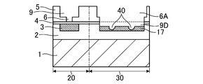
- the first liner film 4 exposed in the pad hole 6A is removed, and the upper portion of the metal film 17 is also removed to form the pad recess 9D. Since the etching rate of copper constituting the metal film 17 is slower than the etching rate of the second interlayer film 5, the depth of the pad recess 9D is set to the pad recess 9A in the semiconductor device of this embodiment (see FIG. 3A). It becomes shallower than In this step, the metal film 17 is greatly damaged by etching.
- the first liner film 4 exposed in the via hole 6 in the element formation region 20 is removed. Also in this step, the metal film 17 is damaged. Subsequently, as shown in FIG. 8A, the reaction product by etching is removed by washing. At this time, a defect 42 is generated in the metal film 17 due to the damage that the metal film 17 receives by etching.
- the pad hole 6A in the pad formation region 30, and the pad recess 9D by plating After the copper is embedded in the via hole 6 and the wiring groove 9 in the element formation region 20, the pad hole 6A in the pad formation region 30, and the pad recess 9D by plating. Then, excess copper is removed by CMP method. As a result, the first via 10 is formed in the via hole 6, and the second metal wiring 11 is formed in the wiring groove 9. In this step, copper is embedded in the pad hole 6A and the pad recess 9D, whereby the landing pad 12B including these copper and the metal film 17 is formed. Therefore, the lower surface position of the landing pad 12B manufactured by the method according to the reference example is equal to the lower surface position of the first metal wiring 3.
- the defects 40 and 42 generated in the metal film 17 during the manufacturing process remain as cavities without being embedded.
- a second liner film 13 made of silicon carbide having a thickness of 60 nm is formed on the second interlayer film 5, the second metal wiring 11, and the landing pad 12B.
- a passivation film 14 made of silicon nitride and having a thickness of 1000 nm is formed on the second liner film 13 by a known CVD method or the like.
- the substrate 1 is shaved from the back surface side so that the thickness of the substrate 1 is about 300 to 400 ⁇ m.
- an insulating film 15 is formed on the back surface of the substrate 1.
- the insulating film 15 and the substrate 1 are etched from the back side by lithography and an etching method.
- a part of the landing pad 12B is etched to form the via hole 16.
- excess copper is removed by CMP to penetrate the substrate 1 and connect a TSV (second via) 25 connected to the landing pad 12B.
- the defects 40 and 42 are generated in the landing pad 12B. Therefore, a connection failure may occur between the landing pad 12B and the TSV 25.
- the position of the lower surface of the landing pad 12 can be set lower than the first metal wiring 3, so that the landing pad 12 can be made thicker than the semiconductor device according to the reference example. It is possible to prevent the landing pad 12 from penetrating when the via hole 16 is formed.
- the formation of the recess for forming the landing pad 12 can be performed simultaneously with the step of forming the wiring groove 9 and the via hole 6, and the formation of the copper film for the landing pad 12 is the second. Since the metal wiring 11 and the first via 10 can be formed at the same time, the landing pad 12 can be formed without increasing the number of steps.
- an element formation region (first region) 20 and a pad formation region (second region) 30 are formed.
- the first interlayer film 2 passes through the second interlayer film 5 and electrically connects the first metal wiring 3 and the second metal wiring 11.
- the semiconductor device of this embodiment is also formed on the second liner film 13 formed on the second interlayer film 5, the second metal wiring 11 and the landing pad 12, and the second liner film 13.
- the passivation film 14 is provided.
- the lower surface position of the landing pad 12 is different from the lower surface position of the first metal wiring 3 and is lower than the lower surface position of the first metal wiring 3.
- the substrate 1 may be made of a semiconductor such as silicon, but is not limited thereto.
- the first interlayer film 2 and the second interlayer film 5 are made of an insulating film such as silicon oxide.
- the first interlayer film 2 and the second interlayer film 5 may be made of an insulator other than silicon oxide, and may be a known low-k film.
- the landing pad 12, the first metal wiring 3 and the second metal wiring 11 may be made of copper or an alloy containing copper as a main component, or may be made of a conductive material other than copper. Good.
- the landing pad 12 may be made of the same material as the second metal wiring 11 and the first via 10.
- the first metal wiring 3, the second metal wiring 11 and the first via, the landing pad 12 and the TSV 25 may each be composed only of copper or the like, but are formed thinly along the inner surface of the wiring groove or recess.
- the barrier metal layer may be composed of two layers of a metal layer made of copper or the like, or may have a structure other than this.
- the thickness of the landing pad 12 is thicker than the total value of the height of the first metal wiring 3, the height of the first via 10, and the height of the second metal wiring 11. ing.
- the landing pad 12 only needs to be provided by using a process of forming two layers of metal wiring adjacent in the vertical direction, and is higher than the total height of at least one layer of metal wiring and vias connected thereto. What is necessary is just to form thickly.
- the thickness of the first interlayer film 2 may be about 400 nm, for example. Further, the landing pad 12 may have a diameter of about 70 ⁇ m and a thickness of about 360 nm to 390 nm.
- FIG. 9A to 9C and 10A to 10C are cross-sectional views illustrating a method for manufacturing a semiconductor device according to the second embodiment.
- the method of the present embodiment is the same as the method of the first embodiment up to the step shown in FIG. 2B. Therefore, the process after the process shown in FIG. 2B will be described below.
- a wiring formation region is opened, and in the pad formation region 30, a resist 8 covering the pad hole 6A is formed.
- the second interlayer film 5 is etched using the resist 8 to form a wiring groove 9 in the element formation region 20.
- the first liner film 4 is not etched in the pad formation region 30.
- the resists 7 and 8 are removed by washing.
- the portion of the first liner film 4 exposed in the via hole 6 is removed by etching. Simultaneously with the removal of the first liner film 4, a part of the first liner film 4 and a part of the first interlayer film 2 are removed in the pad formation region 30, thereby forming a pad recess 9 ⁇ / b> C.
- the via hole 6 and the wiring groove 9 in the element forming region 20, the pad hole 6 A in the pad forming region 30, and the pad recess 9 C are plated by plating.
- excess copper is removed by CMP method.
- the first via 10 is formed in the via hole 6, and the second metal wiring 11 is formed in the wiring groove 9.
- the landing pad 12 is formed in the pad recess 9C and the pad hole 6A. At this time, the lower surface position of the landing pad 12 is shallower than the lower surface position of the first metal wiring 3.
- the thickness of the landing pad 12 is about 240 nm.
- a second liner film 13 made of silicon carbide having a thickness of 60 nm is formed on the second interlayer film 5, the second metal wiring 11, and the landing pad 12.
- a passivation film 14 made of silicon nitride and having a thickness of 1000 nm is formed on the second liner film 13 by a known CVD method or the like.
- the substrate 1 is shaved from the back side so that the thickness of the substrate 1 is about 300 to 400 ⁇ m.
- an insulating film 15 is formed on the back surface of the substrate 1.
- the insulating film 15 and the substrate 1 are etched from the back side by lithography and etching.
- a part of the landing pad 12 is etched to form a via hole 16.
- the excess copper is removed by CMP, whereby a TSV (second via) 25 that penetrates the substrate 1 and is connected to the landing pad 12 is formed.
- the landing pad 12 is formed of a metal film formed at a time, the metal film is not damaged by etching. For this reason, since no defect occurs in the landing pad 12, a connection failure is less likely to occur between the TSV 25 and the landing pad 12.
- the thickness of the landing pad 12 can be made larger than the total value of the height of the first via 10 and the height of the second metal wiring 11, so that when the TSV 25 is formed. It is difficult for the landing pad 12 to penetrate.
- 11A to 11C, 12A to 12C, 13A to 13C, 14A, and 14B are cross-sectional views illustrating a method for manufacturing a semiconductor device according to another embodiment of the present invention.
- a metal film 17 is provided in the pad forming region 30 at the same depth position as the first metal wiring 3.
- a first liner film 4 is formed on the first metal wiring 3, the metal film 17, and the first interlayer film 2.
- the via hole 6 is formed in the element forming region 20, and the via hole 6 ⁇ / b> B is formed in the pad forming region 30.
- the diameters of the via hole 6 and the via hole 6B are the same.
- a resist 7 is formed on the substrate.
- a resist 7 is embedded in the via holes 6 and 6B.
- the resist 7 is etched back to partially leave the resist 7 in the via holes 6 and 6B.
- a resist 8 for forming a wiring groove is formed on the second interlayer film 5. At this time, an opening is formed in the resist 8 in a region where the via hole 6B is formed.
- the second interlayer film 5 is etched using the resist 8 as a mask to form a wiring groove 9. Since the resist 7 remains in the via hole 6B, the metal film 17 is not exposed in this step. By this step, the pad hole 9E is formed in the pad forming region 30.
- the resists 7 and 8 are removed by cleaning.
- the exposed portions of the first liner film 4 are removed by etching in the element formation region 20 and the pad formation region 30.
- the substrate is cleaned.
- the metal film 17 is not easily damaged by etching. For this reason, in the process shown in FIG. 13B, defects are less likely to occur in the metal film 17.
- the excess copper is removed by the CMP method, whereby the first via 10 and the second metal wiring 11, the third via 10A and the metal film 11A are formed.
- the metal film 17, the third via 10A, and the metal film 11A constitute a landing pad 12C.
- a second liner film 13 made of silicon carbide having a thickness of 60 nm is formed on the second interlayer film 5, the second metal wiring 11, and the landing pad 12.
- a passivation film 14 made of silicon nitride and having a thickness of 1000 nm is formed on the second liner film 13 by a known CVD method or the like.
- the substrate 1 is shaved from the back surface side so that the thickness of the substrate 1 is about 300 to 400 ⁇ m.
- an insulating film 15 is formed on the back surface of the substrate 1.
- the insulating film 15 and the substrate 1 are etched from the back side by lithography and etching.
- a part of the first liner film 4 and the second interlayer film 5 is removed, and a part of the landing pad 12C is etched to form a via hole 16.
- excess copper is removed by CMP to penetrate the substrate 1 and connect the TSV (second via) 25 to the landing pad 12C.
- the first liner film 4 and the second interlayer film 5 exist between the via holes 6B in the pad formation region 30, when forming the via holes 16, It is difficult to reliably stop etching on the landing pad 12C.
- the semiconductor device and the manufacturing method thereof described above are examples of the embodiment, and the configuration of the semiconductor device, the thickness, size, material, and the like of each layer can be changed as appropriate.
- the size of the opening of the resist 8 in the pad formation region 30 may be larger than the pad hole 6A, but may be the same size as the pad hole 6A or smaller than the pad hole 6A.
- the semiconductor device and the manufacturing method thereof according to the present invention can be applied to various semiconductor devices provided with a TSV structure.
Landscapes
- Engineering & Computer Science (AREA)
- Physics & Mathematics (AREA)
- Condensed Matter Physics & Semiconductors (AREA)
- General Physics & Mathematics (AREA)
- Computer Hardware Design (AREA)
- Microelectronics & Electronic Packaging (AREA)
- Power Engineering (AREA)
- Manufacturing & Machinery (AREA)
- Internal Circuitry In Semiconductor Integrated Circuit Devices (AREA)
Abstract
Description
本発明は、through-silicon-via(TSV)用のランディングパッドを備えた半導体装置及びその製造方法に関するものである。 The present invention relates to a semiconductor device having a landing pad for through-silicon-via (TSV) and a method for manufacturing the same.
近年、デバイスの微細化及び高集積化に伴い、チップを縦方向に積層する三次元実装技術の開発が進み、基板を貫通して垂直方向に電気的接続を形成するTSV技術が重要になってきている。 In recent years, with the miniaturization and high integration of devices, the development of three-dimensional mounting technology for stacking chips vertically has progressed, and TSV technology that forms electrical connections in the vertical direction through the substrate has become important. ing.
このようなTSV構造において、TSVと接続するTSV用ランディングパッドの厚さを厚くすることにより、TSVを形成する際のパッドの突き抜けを防ぐ要求がある。この要求に対して、特許文献1には、2層もしくはそれ以上の金属膜を積層することによって厚いTSV用ランディングパッドを形成する技術が記載されている。
In such a TSV structure, there is a need to prevent penetration of the pad when forming the TSV by increasing the thickness of the landing pad for TSV connected to the TSV. In response to this requirement,
しかしながら、TSV構造において、2層もしくはそれ以上の金属層を積層することによってTSV用ランディングパッドを形成する従来の技術では、ランディングパッドとTSVとの間で接続不良が生じる場合がある。 However, in the conventional technique in which a TSV landing pad is formed by laminating two or more metal layers in a TSV structure, a connection failure may occur between the landing pad and the TSV.
具体的に、従来の技術では、1層目の金属膜を形成後、2層目以降の金属膜を形成するためのエッチング工程によって1層目の金属膜がダメージを受けやすくなっている。そのため、エッチング工程後の洗浄工程によって1層目の金属膜のうちダメージを受けた部分が流失し、2層目の金属膜を形成する際に空洞が生じる可能性がある。このように、1層目の金属膜と2層目の金属膜との間に空洞が生じると、TSV用ランディングパッドのTSVとの接続部において電気特性が悪くなり、信頼性が低下する可能性がある。 Specifically, in the conventional technique, after the first metal film is formed, the first metal film is easily damaged by the etching process for forming the second and subsequent metal films. Therefore, the damaged part of the first metal film may be washed away by the cleaning process after the etching process, and a cavity may be generated when the second metal film is formed. As described above, when a cavity is formed between the first metal film and the second metal film, the electrical characteristics at the connection portion of the TSV landing pad with the TSV may be deteriorated and reliability may be lowered. There is.
本発明の目的は、TSVの形成時にランディングパッドの突き抜けが防がれるとともに、TSVとランディングパッドとの良好な電気的接続を確保できる半導体装置を提供することにある。 An object of the present invention is to provide a semiconductor device that can prevent a landing pad from penetrating during formation of a TSV and can ensure a good electrical connection between the TSV and the landing pad.
本明細書に開示された半導体装置は、第1の領域と、第2の領域とが形成された基板と、前記基板の上面上に形成された第1の層間膜と、前記第1の領域において、前記第1の層間膜の上部に埋め込まれた第1の金属配線と、前記第1の層間膜上及び前記第1の金属配線上に形成された第2の層間膜と、前記第1の領域において、前記第2の層間膜の上部に埋め込まれた第2の金属配線と、前記第2の層間膜を貫通し、前記第1の金属配線と前記第2の金属配線とを電気的に接続する第1のビアと、前記第2の領域において、前記第1の層間膜の上部に埋め込まれるとともに、前記第2の層間膜を貫通するランディングパッドと、前記第2の領域において、前記基板の裏面側から前記基板及び前記第1の層間膜を貫通し、前記ランディングパッドに接続する第2のビアとを備えている。前記ランディングパッドの下面位置は、前記第1の金属配線の下面位置と異なっている。 The semiconductor device disclosed in this specification includes a substrate in which a first region and a second region are formed, a first interlayer film formed on an upper surface of the substrate, and the first region. The first metal wiring buried in the upper portion of the first interlayer film, the second interlayer film formed on the first interlayer film and on the first metal wiring, and the first In this region, the second metal wiring buried above the second interlayer film, and the second metal wiring penetrating the second interlayer film are electrically connected to each other. A first via that connects to the first interlayer film, a landing pad that is buried in the upper portion of the first interlayer film and penetrates the second interlayer film, and the second area, The landing through the substrate and the first interlayer film from the back side of the substrate, And a second via that connects to the head. The position of the lower surface of the landing pad is different from the position of the lower surface of the first metal wiring.
本明細書に開示された半導体装置及びその製造方法によれば、TSVの形成時にランディングパッドの突き抜けが防がれるとともに、TSVとランディングパッドとの良好な電気的接続を実現しうる。 According to the semiconductor device and the manufacturing method thereof disclosed in this specification, it is possible to prevent the landing pad from penetrating during the formation of the TSV, and to realize a good electrical connection between the TSV and the landing pad.
以下、本発明の実施形態を図面に基づいて詳細に説明する。 Hereinafter, embodiments of the present invention will be described in detail with reference to the drawings.
(第1の実施形態)
-半導体装置の製造方法-
図1A~C、図2A~C、図3A~C及び図4A~Dは、第1の実施形態に係る半導体装置の製造方法を説明するための断面図である。これらの図では、左側が素子形成領域20(第1の領域)、右側がパッド形成領域30(第2の領域)となっている。以下、半導体装置の製造方法を説明する。
(First embodiment)
-Semiconductor device manufacturing method-
1A to 1C, 2A to 2C, 3A to 3C, and 4A to 4D are cross-sectional views for explaining the method for manufacturing the semiconductor device according to the first embodiment. In these drawings, the left side is an element formation region 20 (first region), and the right side is a pad formation region 30 (second region). Hereinafter, a method for manufacturing a semiconductor device will be described.
まず、図1Aに示すように、素子形成領域20とパッド形成領域30とが形成された基板1の上面上にchemical vapor deposition(CVD)法等により酸化ケイ素(SiO2)等の絶縁体からなる第1の層間膜2を形成する。次いで、第2の層間膜2の上部に公知のリソグラフィ及びエッチングによって配線溝を形成する。次に、めっき法により当該配線溝内に銅等の金属を埋め込んだ後、chemical mechanical polishing(CMP)法等により余剰の金属を除去することにより、配線溝内に埋め込まれた厚さ約120nm程度の第1の金属配線3を形成する。この際の第1の層間膜2の厚さは、例えば400nmである。
First, as shown in FIG. 1A, an insulator such as silicon oxide (SiO 2 ) is formed on the upper surface of the
一方、パッド形成領域30では、第1の金属配線3に相当する金属層を形成しない。
On the other hand, no metal layer corresponding to the
続いて、第1の金属配線3の上及び第1の層間膜2の上に、公知の方法により、例えば炭化ケイ素(SiC)からなる厚さ60nmの第1のライナー膜4を形成する。
Subsequently, a
次に、図1Bに示すように、第1の層間膜2上及び第1の金属配線3上に第1のライナー膜4を挟んで酸化ケイ素からなる厚さ300nmの第2の層間膜5を形成する。
Next, as shown in FIG. 1B, a
次いで、図1Cに示すように、リソグラフィ及びエッチングによって、素子形成領域20における第1の金属配線3の上方に、第2の層間膜5を貫通するビアホール6を形成する。ビアホール6の形成と同時に、パッド形成領域30において第2の層間膜5を貫通するパッド用孔6Aを形成する。ビアホール6の直径は約100nmであり、パッド用孔6Aの直径は約70μmである。ビアホール6とパッド用孔6Aとは、同一のマスク(図示せず)を用いたエッチングにより形成できる。このエッチングは、第1のライナー膜4で止める。
Next, as shown in FIG. 1C, a via
次に、図2Aに示すように、基板上に厚さ約300nmのレジスト7を形成する。素子形成領域20におけるビアホール6の開口面積は小さいため、レジスト7はビアホール6内に完全に埋め込まれ、ビアホール6内のレジストも含めほぼ600nmの厚さに形成される。一方、パッド形成領域30に形成されたパッド用孔6Aの平面面積はビアホール6よりも広いので、パッド用孔6A上ではレジスト7の厚さは約300nmとなり、ビアホール6上でのレジスト7の厚さに比べて薄くなっている。
Next, as shown in FIG. 2A, a resist 7 having a thickness of about 300 nm is formed on the substrate. Since the opening area of the via
次に、図2Bに示すように、レジスト7をエッチバックすることにより、レジスト7のうち第2の層間膜5上及びパッド用孔6A内に形成された部分を除去する。この工程では、ビアホール6内にレジスト7が残るが、パッド用孔6A内にはほとんどレジスト7が残らない。
Next, as shown in FIG. 2B, the resist 7 is etched back to remove portions of the resist 7 formed on the
次に、図2Cに示すように、リソグラフィにより素子形成領域20では配線形成領域が開口し、パッド形成領域30ではパッド用孔6Aの上方を開口するレジスト8を形成する。パッド用孔6Aの上方に設けられた開口は、パッド用孔6Aよりも大きい平面面積を有していてもよい。
Next, as shown in FIG. 2C, a resist 8 is formed by lithography so that the wiring formation region is opened in the
次いで、図3Aに示すように、レジスト8を用いて第2の層間膜5をエッチングすることにより、素子形成領域20に配線溝9を形成する。配線溝9の深さは約180nmである。ビアホール6内にはレジスト7が残っているため、ビアホール6が形成された領域では第1のライナー膜4はエッチングされない。
Next, as shown in FIG. 3A, the
また、配線溝9と同時にパッド形成領域30では第1のライナー膜4及び第1の層間膜2の上部が除去されてパッド用凹部9Aが形成される。パッド用凹部9Aでのエッチング量は約120~150nmである。
In addition, in the
次に、図3Bに示すように、洗浄によりレジスト7、8を除去する。 Next, as shown in FIG. 3B, the resists 7 and 8 are removed by washing.
続いて、図3Cに示すように、エッチングにより第1のライナー膜4のうちビアホール6内に露出する部分を除去する。また、第1のライナー膜4の除去と同時にパッド形成領域30において第1の層間膜2の一部が除去され、パッド用凹部9Bが形成される。パッド用凹部9Bの深さは約70nmである。
Subsequently, as shown in FIG. 3C, a portion of the
次に、図4Aに示すように、エッチングによる反応生成物を洗浄により除去する。本工程の洗浄により、半導体装置の形状は変わらない。 Next, as shown in FIG. 4A, etching reaction products are removed by washing. The shape of the semiconductor device is not changed by the cleaning in this step.
次に、図4Bに示すように、めっき法により、素子形成領域20におけるビアホール6内及び配線溝9内、パッド形成領域30におけるパッド用孔6A内、パッド用凹部9A、9B内に銅を埋め込んだ後、CMP法により余剰の銅を除去する。これにより、ビアホール6内に第1のビア10を形成し、配線溝9内に第2の金属配線11を形成する。また、パッド用凹部9A、9B内及びパッド用孔6A内にランディングパッド12を形成する。この際に、ランディングパッド12の下面位置は、第1の金属配線3の下面位置よりも深くなっている。
Next, as shown in FIG. 4B, copper is embedded in the via
第1のビア10の高さは約110nmであり、第2の金属配線11の高さは約120nmである。また、ランディングパッド12の高さ(厚さ)は約360nm~390nmである。その後、第2の層間膜5上、第2の金属配線11上及びランディングパッド12上に厚さ60nmの炭化ケイ素からなる第2のライナー膜13を形成する。
The height of the first via 10 is about 110 nm, and the height of the
次に、図4Cに示すように、第2のライナー膜13上に、公知のCVD法等により窒化ケイ素からなる厚さ1000nmのパッシベーション膜14を形成する。以上で、基板1の上面側の加工は一旦完了する。
Next, as shown in FIG. 4C, a
次に、図4Dに示すように、基板1を裏面側から削って基板1の厚さを約300~400μmにする。次いで、基板1の裏面上に、素子形成領域20を覆い、例えば、酸化ケイ素膜等からなる絶縁膜15を形成する。その後、リソグラフィとエッチング法とにより、絶縁膜15と基板1とを裏面側からエッチングする。この際には、ランディングパッド12の一部までエッチングを行い、ビアホール16を形成する。次いで、公知のめっき法等によりビアホール16内に銅を埋め込んだ後、CMPにより余剰の銅を除去することにより、基板1を貫通し、ランディングパッド12に接続するTSV(第2のビア)25を形成する。ビアホール16内に形成する金属は、タングステン(W)やアルミニウム(Al)等であってもよいし、ビアホール16内が完全に金属で埋め込まれていなくてもよい。以上の工程により、本実施形態の半導体装置を作製することができる。
Next, as shown in FIG. 4D, the
次に、上述の方法によってランディングパッド12を形成した理由を、参考例に係る製造方法と比較しながら説明する。
Next, the reason why the
図5A~C、図6A~C、図7A~C及び図8A~Dは、参考例に係る半導体装置の製造方法を説明する断面図である。 FIGS. 5A to 5C, FIGS. 6A to 6C, FIGS. 7A to C, and FIGS. 8A to 8D are cross-sectional views illustrating a method of manufacturing a semiconductor device according to a reference example.
本参考例では、図5Aに示すように、素子形成領域20とパッド形成領域30とが形成された基板1の上面上に酸化ケイ素等の絶縁体からなる第1の層間膜2を形成する。次いで、第1の層間膜2の上部に公知のリソグラフィ及びエッチングによって配線溝を形成する。この際に、パッド形成領域30においても素子形成領域20内の配線溝と同じ深さの凹部を形成する。
In this reference example, as shown in FIG. 5A, the
続いて、めっき法により基板上に銅を堆積し、その後CMP法により余剰の銅を除去することにより、素子形成領域20に第1の金属配線3を形成するとともに、パッド形成領域30に金属膜17を形成する。
Subsequently, copper is deposited on the substrate by a plating method, and then excess copper is removed by a CMP method, thereby forming the
次に、図5Bに示すように、第1の層間膜2上及び第1の金属配線3上に第1のライナー膜4を挟んで酸化ケイ素からなる厚さ300nmの第2の層間膜5を形成する。次いで、図5Cに示すように、素子形成領域20においては第2の層間膜5を貫通するビアホール6を形成するとともに、パッド形成領域30においては金属膜17の上方にパッド用孔6Aを形成する。
Next, as shown in FIG. 5B, a
次に、図6Aに示すように、基板上に厚さ約300nmのレジスト7を形成する。レジスト7はビアホール6内及びパッド用孔6A内に埋め込まれる。次に、図6Bに示すように、レジスト7をエッチバックすることにより、レジスト7のうち第2の層間膜5上及びパッド用孔6A内に形成された部分を除去する。
Next, as shown in FIG. 6A, a resist 7 having a thickness of about 300 nm is formed on the substrate. The resist 7 is embedded in the via
次に、図6Cに示すように、リソグラフィにより配線形成用のレジスト8を形成する。次いで、図7Aに示すように、素子形成領域20に配線溝9を形成する。この際に、パッド形成領域30では、パッド用孔6A内に露出する第1のライナー膜4が除去されるとともに、金属膜17の上部も除去されてパッド用凹部9Dが形成される。金属膜17を構成する銅のエッチングレートは第2の層間膜5のエッチングレートよりも遅いため、パッド用凹部9Dの深さは、本実施形態の半導体装置におけるパッド用凹部9A(図3A参照)に比べて浅くなる。なお、本工程では、金属膜17がエッチングにより大きなダメージを受ける。
Next, as shown in FIG. 6C, a resist 8 for wiring formation is formed by lithography. Next, as shown in FIG. 7A, a
次に、図7Bに示すように、洗浄によりレジスト7を除去する際に、エッチングによるダメージを受けた金属膜17の一部から銅が流出し、欠陥40が形成される。
Next, as shown in FIG. 7B, when the resist 7 is removed by cleaning, copper flows out from a part of the
次に、図7Cに示すように、素子形成領域20においてビアホール6内に露出する第1のライナー膜4を除去する。本工程においても、金属膜17はダメージを受ける。続いて、図8Aに示すように、エッチングによる反応生成物を洗浄により除去する。この際に、金属膜17がエッチングによって受けたダメージにより、金属膜17に欠陥42が生じる。
Next, as shown in FIG. 7C, the
次に、図8Bに示すように、めっき法により、素子形成領域20におけるビアホール6内及び配線溝9内、パッド形成領域30におけるパッド用孔6A内、パッド用凹部9D内に銅を埋め込んだ後、CMP法により余剰の銅を除去する。これにより、ビアホール6内に第1のビア10を形成し、配線溝9内に第2の金属配線11を形成する。本工程では、パッド用孔6A内及びパッド用凹部9D内に銅が埋め込まれることにより、これらの銅及び金属膜17を含むランディングパッド12Bが形成される。従って、参考例に係る方法で作製されたランディングパッド12Bの下面位置は、第1の金属配線3の下面位置と等しくなっている。
Next, as shown in FIG. 8B, after the copper is embedded in the via
参考例に係る方法では、製造工程中に金属膜17に生じた欠陥40、42が埋め込まれずに空洞として残る。
In the method according to the reference example, the
次いで、第2の層間膜5上、第2の金属配線11上及びランディングパッド12B上に厚さ60nmの炭化ケイ素からなる第2のライナー膜13を形成する。
Next, a
この後、図8Cに示すように、第2のライナー膜13上に、公知のCVD法等により窒化ケイ素からなる厚さ1000nmのパッシベーション膜14を形成する。次に、図8Dに示すように、基板1を裏面側から削って基板1の厚さを約300~400μmにする。次いで、基板1の裏面上に、絶縁膜15を形成する。続いて、リソグラフィとエッチング法とにより、絶縁膜15と基板1とを裏面側からエッチングする。この際には、ランディングパッド12Bの一部までエッチングを行い、ビアホール16を形成する。次いで、公知のめっき法等によりビアホール16内に銅を埋め込んだ後、CMPにより余剰の銅を除去することにより、基板1を貫通し、ランディングパッド12Bに接続するTSV(第2のビア)25を形成する。
Thereafter, as shown in FIG. 8C, a
参考例に係る半導体装置では、ランディングパッド12B内に欠陥40、42が生じるので、ランディングパッド12BとTSV25との間で接続不良を起こす場合がある。
In the semiconductor device according to the reference example, the
一方、本実施形態の半導体装置では、ランディングパッド12内にエッチングによるダメージが入らないので、ランディングパッド12とTSV25との間に接続不良は起こらない。また、本実施形態の半導体装置では、ランディングパッド12の下面位置を第1の金属配線3よりも低い位置にすることができるので、参考例に係る半導体装置よりもランディングパッド12を厚くすることができ、ビアホール16を形成する際にランディングパッド12の突き抜けが生じにくくなっている。
On the other hand, in the semiconductor device of this embodiment, no damage is caused by etching in the
また、本実施形態の方法では、ランディングパッド12を形成するための凹部の形成は配線溝9やビアホール6を形成する工程と同時に行うことができ、ランディングパッド12用の銅膜の形成は第2の金属配線11及び第1のビア10の形成と同時に行うことができるので、工程を増やすことなくランディングパッド12を形成することができる。
Further, in the method of the present embodiment, the formation of the recess for forming the
-半導体装置の構成-
以上の方法によって作製される本実施形態実施形態の半導体装置は、図4Dに示すように、素子形成領域(第1の領域)20と、パッド形成領域(第2の領域)30とが形成された基板1と、基板1の上面上に形成された第1の層間膜2と、素子形成領域20において、第1の層間膜2の上部に埋め込まれた第1の金属配線3と、第1の層間膜2上及び第1の金属配線3上に形成された第2の層間膜5と、素子形成領域20において、第2の層間膜5の上部に埋め込まれた第2の金属配線11と、第2の層間膜5を貫通し、第1の金属配線3と第2の金属配線11とを電気的に接続する第1のビア10と、パッド形成領域30において、第1の層間膜2の上部に埋め込まれるとともに、第2の層間膜5を貫通するランディングパッド12と、パッド形成領域30において、基板1の裏面側から基板1及び第1の層間膜2を貫通し、ランディングパッド12に接続するTSV(第2のビア)25とを備えている。本実施形態の半導体装置はまた、第2の層間膜5上、第2の金属配線11上及びランディングパッド12上に形成された第2のライナー膜13と、第2のライナー膜13上に形成されたパッシベーション膜14とを備えている。
-Structure of semiconductor device-
As shown in FIG. 4D, in the semiconductor device of this embodiment manufactured by the above method, an element formation region (first region) 20 and a pad formation region (second region) 30 are formed. The
ランディングパッド12の下面位置は、第1の金属配線3の下面位置と異なっており、第1の金属配線3の下面位置よりも低い位置にある。
The lower surface position of the
基板1は、シリコン等の半導体で構成されていてもよいが、これに限定されない。第1の層間膜2及び第2の層間膜5は、例えば酸化ケイ素等の絶縁膜で構成されている。第1の層間膜2及び第2の層間膜5は酸化ケイ素以外の絶縁体で構成されていてもよく、公知のLow-k膜であってもよい。
The
ランディングパッド12、第1の金属配線3及び第2の金属配線11は、銅又は銅を主成分とする合金等で構成されていてもよいし、銅以外の導電性物質で構成されていてもよい。ランディングパッド12は、第2の金属配線11及び第1のビア10と同じ材料で構成されていてもよい。
The
第1の金属配線3、第2の金属配線11及び第1のビア、ランディングパッド12及びTSV25は、それぞれ銅等のみで構成されていてもよいが、配線溝又は凹部の内面に沿って薄く形成されたバリアメタル層と、銅等からなる金属層との二層で構成されていてもよく、これ以外の構成を有していてもよい。
The
本実施形態の半導体装置では、ランディングパッド12の厚みは、第1の金属配線3の高さと、第1のビア10の高さと、第2の金属配線11の高さの合計値よりも厚くなっている。
In the semiconductor device of this embodiment, the thickness of the
また、本実施形態の半導体装置では、二層の金属配線層が設けられた例を示しているが、さらに多層の金属配線が設けられていてもよい。この場合、ランディングパッド12は、上下で隣り合う2層の金属配線を形成する工程を利用して設けられていればよく、少なくとも1層の金属配線とこれに接続されたビアの合計高さよりも厚く形成されていればよい。
In the semiconductor device of this embodiment, an example in which two metal wiring layers are provided is shown, but a multilayer metal wiring may be provided. In this case, the
第1の層間膜2の厚さは例えば400nm程度であってもよい。また、ランディングパッド12の直径は約70μm程度であってもよく、厚さは約360nm~390nm程度であってもよい。
The thickness of the
(第2の実施形態)
本発明の第2の実施形態に係る半導体装置の製造方法を説明する。
(Second Embodiment)
A method for manufacturing a semiconductor device according to the second embodiment of the present invention will be described.
図9A~C、図10A~Cは、第2の実施形態に係る半導体装置の製造方法を説明する断面図である。本実施形態の方法は、図2Bに示す工程まで第1の実施形態の方法と同じである。従って、図2Bに示す工程の後の工程について、以下に説明する。 9A to 9C and 10A to 10C are cross-sectional views illustrating a method for manufacturing a semiconductor device according to the second embodiment. The method of the present embodiment is the same as the method of the first embodiment up to the step shown in FIG. 2B. Therefore, the process after the process shown in FIG. 2B will be described below.
図9Aに示すように、素子形成領域20では配線形成領域が開口し、パッド形成領域30ではパッド用孔6Aを覆うレジスト8を形成する。
As shown in FIG. 9A, in the
次に、図9Bに示すように、レジスト8を用いて第2の層間膜5をエッチングすることにより、素子形成領域20に配線溝9を形成する。この際に、パッド形成領域30では第1のライナー膜4はエッチングされない。
Next, as shown in FIG. 9B, the
次に、図9Cに示すように、洗浄によりレジスト7、8を除去する。 Next, as shown in FIG. 9C, the resists 7 and 8 are removed by washing.
次に、図10Aに示すように、エッチングにより第1のライナー膜4のうちビアホール6内に露出する部分を除去する。また、第1のライナー膜4の除去と同時にパッド形成領域30において第1のライナー膜4の一部及び第1の層間膜2の一部が除去され、パッド用凹部9Cが形成される。
Next, as shown in FIG. 10A, the portion of the
続いて、図10Bに示すように、基板を洗浄後、めっき法により、素子形成領域20内のビアホール6内及び配線溝9内、パッド形成領域30内のパッド用孔6A内及びパッド用凹部9C内に銅を埋め込んだ後、CMP法により余剰の銅を除去する。これにより、ビアホール6内に第1のビア10を形成し、配線溝9内に第2の金属配線11を形成する。また、パッド用凹部9C内及びパッド用孔6A内にランディングパッド12を形成する。この際に、ランディングパッド12の下面位置は、第1の金属配線3の下面位置よりも浅くなっている。ランディングパッド12の厚さは、約240nmである。
Subsequently, as shown in FIG. 10B, after the substrate is cleaned, the via
その後、第2の層間膜5上、第2の金属配線11上及びランディングパッド12上に厚さ60nmの炭化ケイ素からなる第2のライナー膜13を形成する。
Thereafter, a
次に、図10Cに示すように、第2のライナー膜13上に、公知のCVD法等により窒化ケイ素からなる厚さ1000nmのパッシベーション膜14を形成する。次いで、基板1を裏面側から削って基板1の厚さを約300~400μmにする。続いて、基板1の裏面上に、絶縁膜15を形成する。その後、リソグラフィとエッチング法とにより絶縁膜15と基板1とを裏面側からエッチングする。この際には、ランディングパッド12の一部までエッチングを行い、ビアホール16を形成する。次いで、公知のめっき法等によりビアホール16内に銅を埋め込んだ後、CMPにより余剰の銅を除去することにより、基板1を貫通し、ランディングパッド12に接続するTSV(第2のビア)25を形成する。
Next, as shown in FIG. 10C, a
以上の方法によっても、ランディングパッド12は一度に形成した金属膜で形成されるので、当該金属膜がエッチングによるダメージを受けることがない。このため、ランディングパッド12内に欠陥が生じることがないので、TSV25とランディングパッド12との間に接続不良が生じにくくなっている。
Also by the above method, since the
また、本実施形態の方法によれば、ランディングパッド12の厚みを第1のビア10の高さと第2の金属配線11の高さとの合計値よりも厚くすることができるので、TSV25の形成時にランディングパッド12の突き抜けが生じにくくなっている。
Further, according to the method of the present embodiment, the thickness of the
(その他の実施形態)
図11A~C、図12A~C、図13A~C、図14A、Bは、本発明の他の実施形態に係る半導体装置の製造方法を説明する断面図である。
(Other embodiments)
11A to 11C, 12A to 12C, 13A to 13C, 14A, and 14B are cross-sectional views illustrating a method for manufacturing a semiconductor device according to another embodiment of the present invention.
ここでは、パッド形成領域30内に素子形成領域20内と同じサイズのビアホール6Bを形成する場合の半導体装置について説明する。
Here, a semiconductor device when the via
図11Aに示すように、パッド形成領域30内には、第1の金属配線3と同じ深さ位置に金属膜17が設けられている。第1の金属配線3上、金属膜17上及び第1の層間膜2上に第1のライナー膜4を形成する。次いで、第1のライナー膜4上に第2の層間膜5を形成した後、素子形成領域20にはビアホール6を形成し、パッド形成領域30にはビアホール6Bを形成する。ここで、ビアホール6とビアホール6Bの径は同じである。
As shown in FIG. 11A, a
次に、図11Bに示すように、基板上にレジスト7を形成する。本工程では、ビアホール6、6B内にレジスト7が埋め込まれる。次いで、図11Cに示すように、レジスト7をエッチバックすることにより、ビアホール6、6B内にレジスト7を部分的に残す。 Next, as shown in FIG. 11B, a resist 7 is formed on the substrate. In this step, a resist 7 is embedded in the via holes 6 and 6B. Next, as shown in FIG. 11C, the resist 7 is etched back to partially leave the resist 7 in the via holes 6 and 6B.
次いで、図12Aに示すように、配線溝を形成するためのレジスト8を第2の層間膜5上に形成する。この際に、レジスト8には、ビアホール6Bが形成された領域に開口が形成される。
Next, as shown in FIG. 12A, a resist 8 for forming a wiring groove is formed on the
次に、図12Bに示すように、レジスト8をマスクとして第2の層間膜5をエッチングし、配線溝9を形成する。ビアホール6B内にはレジスト7が残っているので、本工程において金属膜17が露出することはない。本工程により、パッド形成領域30では、パッド用孔9Eが形成される。
Next, as shown in FIG. 12B, the
次いで、図12Cに示すように、洗浄によりレジスト7、8を除去する。続いて、図13Aに示すように、素子形成領域20内及びパッド形成領域30内で、第1のライナー膜4のうち露出している部分をエッチングにより除去する。次いで、図13Bに示すように、基板を洗浄する。図13Aに示す工程では、素子形成領域20とパッド形成領域30とで同じ厚さの第1のライナー膜4を除去するので、金属膜17がエッチングによりダメージを受けにくくなっている。このため、図13Bに示す工程では、金属膜17に欠陥が発生しにくくなっている。
Next, as shown in FIG. 12C, the resists 7 and 8 are removed by cleaning. Subsequently, as shown in FIG. 13A, the exposed portions of the
次に、図13Cに示すように、めっき法によってビアホール6、6B、配線溝9、パッド用孔9E内に銅を埋め込んだ後、CMP法によって余剰の銅を除去することにより、第1のビア10及び第2の金属配線11、第3のビア10A及び金属膜11Aを形成する。ここで、金属膜17、第3のビア10A及び金属膜11Aはランディングパッド12Cを構成する。その後、第2の層間膜5上、第2の金属配線11上及びランディングパッド12上に厚さ60nmの炭化ケイ素からなる第2のライナー膜13を形成する。
Next, as shown in FIG. 13C, after the copper is buried in the via holes 6 and 6B, the
次に、図14Aに示すように、第2のライナー膜13上に、公知のCVD法等により窒化ケイ素からなる厚さ1000nmのパッシベーション膜14を形成する。次いで、図14Bに示すように、基板1を裏面側から削って基板1の厚さを約300~400μmにする。続いて、基板1の裏面上に絶縁膜15を形成する。その後、リソグラフィとエッチング法とにより絶縁膜15と基板1とを裏面側からエッチングする。この際には、第1のライナー膜4及び第2の層間膜5の一部を除去するとともに、ランディングパッド12Cの一部までエッチングを行い、ビアホール16を形成する。次いで、公知のめっき法等によりビアホール16内に銅を埋め込んだ後、CMPにより余剰の銅を除去することにより、基板1を貫通し、ランディングパッド12Cに接続するTSV(第2のビア)25を形成する。
Next, as shown in FIG. 14A, a
本実施形態の方法によっても、ランディングパッド12Cの内部に欠陥が生じないので、ランディングパッド12CとTSV25との間の接続不良を抑えることができる。
Also according to the method of the present embodiment, no defect occurs in the
ただし、本実施形態の方法によれば、パッド形成領域30において、ビアホール6B間には第1のライナー膜4及び第2の層間膜5が存在しているので、ビアホール16を形成する際に、ランディングパッド12C上で確実にエッチングを停止しにくくなっている。
However, according to the method of the present embodiment, since the
このため、パッド形成領域30に小さい径のビアを形成するのは好ましくない。従って、パッド形成領域30内では、素子形成領域20内の第1のビア10よりも径の大きいビアを形成することが好ましい。
For this reason, it is not preferable to form a via having a small diameter in the
なお、以上で説明した半導体装置及びその製造方法は、実施形態の一例であって、半導体装置の構成、各層の膜厚やサイズ、材質等は適宜変更可能である。例えば、パッド形成領域30におけるレジスト8の開口のサイズはパッド用孔6Aよりも大きくてもよいが、パッド用孔6Aと同じ又はパッド用孔6A以下のサイズであってもよい。
Note that the semiconductor device and the manufacturing method thereof described above are examples of the embodiment, and the configuration of the semiconductor device, the thickness, size, material, and the like of each layer can be changed as appropriate. For example, the size of the opening of the resist 8 in the
本発明に係る半導体装置及びその製造方法は、TSV構造を設けた様々な半導体装置に適用できる。 The semiconductor device and the manufacturing method thereof according to the present invention can be applied to various semiconductor devices provided with a TSV structure.
1 基板
2 第1の層間膜
3 第1の金属配線
4 第1のライナー膜
5 第2の層間膜
6、6B ビアホール
6A パッド用孔
7、8 レジスト
9 配線溝
9A、9B、9C、9D パッド用凹部
9E パッド用孔
10 第1のビア
10A 第3のビア
11 第2の金属配線
11A 金属膜
12、12B、12C ランディングパッド
13 第2のライナー膜
14 パッシベーション膜
15 絶縁膜
16 ビアホール
17 金属膜
20 素子形成領域
25 TSV
30 パッド形成領域
40、42 欠陥
DESCRIPTION OF
30
Claims (8)
前記基板の上面上に形成された第1の層間膜と、
前記第1の領域において、前記第1の層間膜の上部に埋め込まれた第1の金属配線と、
前記第1の層間膜上及び前記第1の金属配線上に形成された第2の層間膜と、
前記第1の領域において、前記第2の層間膜の上部に埋め込まれた第2の金属配線と、
前記第2の層間膜を貫通し、前記第1の金属配線と前記第2の金属配線とを電気的に接続する第1のビアと、
前記第2の領域において、前記第1の層間膜の上部に埋め込まれるとともに、前記第2の層間膜を貫通するランディングパッドと、
前記第2の領域において、前記基板の裏面側から前記基板及び前記第1の層間膜を貫通し、前記ランディングパッドに接続する第2のビアとを備え、
前記ランディングパッドの下面位置は、前記第1の金属配線の下面位置と異なっている半導体装置。 A substrate on which a first region and a second region are formed;
A first interlayer film formed on the upper surface of the substrate;
A first metal wiring buried in an upper portion of the first interlayer film in the first region;
A second interlayer film formed on the first interlayer film and on the first metal wiring;
A second metal wiring buried in an upper portion of the second interlayer film in the first region;
A first via that penetrates through the second interlayer film and electrically connects the first metal wiring and the second metal wiring;
A landing pad embedded in the upper portion of the first interlayer film and penetrating through the second interlayer film in the second region;
A second via that penetrates the substrate and the first interlayer film from the back side of the substrate in the second region and connects to the landing pad;
A semiconductor device in which a lower surface position of the landing pad is different from a lower surface position of the first metal wiring.
前記第1のビアと前記第2の金属配線とは同一の材料で構成されており、
前記ランディングパッドは、前記第1の層間膜の上部から前記第2の層間膜内に亘って設けられ、且つ前記第1のビア及び前記第2の金属配線と同一の材料で構成されている金属膜を有していることを特徴とする半導体装置。 In claim 1,
The first via and the second metal wiring are made of the same material,
The landing pad is provided from the upper part of the first interlayer film to the second interlayer film, and is made of the same material as the first via and the second metal wiring. A semiconductor device including a film.
前記ランディングパッドの下面位置は、前記第1の金属配線の下面位置よりも低く、前記ランディングパッドの厚みは、前記第1の金属配線の高さと、前記第1のビアの高さと、前記第2の金属配線の高さとの和よりも厚いことを特徴とする半導体装置。 In claim 1 or 2,
The lower surface position of the landing pad is lower than the lower surface position of the first metal wiring, and the thickness of the landing pad includes the height of the first metal wiring, the height of the first via, and the second height. A semiconductor device characterized in that it is thicker than the sum of the metal wiring heights.
前記第1の層間膜上及び前記第1の金属配線上に、第2の層間膜を形成する工程と、
前記第1の領域において、前記第2の層間膜内の配線溝と、前記第1の金属配線の上方で前記第2の層間膜を貫通する第1のビアホールとをそれぞれ形成する工程と、
前記配線溝及び前記第1のビアホールを形成する際に、前記第2の領域において、前記第1の層間膜の上部にパッド用凹部を形成するとともに、前記第2の層間膜を貫通するパッド用孔を形成する工程と、
前記第1のビアホール、前記配線溝、前記パッド用凹部及び前記パッド用孔内に金属を埋め込むことによって前記第1のビアホール内に第1のビアを形成するとともに、前記配線溝内に第2の金属配線を形成し、且つ前記パッド用凹部及び前記パッド用孔内にランディングパッドを形成する工程と、
前記第2の領域において、前記基板の裏面側から前記基板及び前記第1の層間膜を貫通し、前記ランディングパッドに接続する第2のビアを形成する工程とを備えている半導体装置の製造方法。 Forming a first interlayer film on the upper surface of the substrate on which the first region and the second region are formed, and a first metal wiring buried above the first interlayer film;
Forming a second interlayer film on the first interlayer film and on the first metal wiring;
Forming a wiring trench in the second interlayer film in the first region and a first via hole penetrating the second interlayer film above the first metal wiring;
When forming the wiring trench and the first via hole, a pad recess is formed on the first interlayer film in the second region, and for the pad penetrating the second interlayer film. Forming a hole;
A first via is formed in the first via hole by embedding a metal in the first via hole, the wiring groove, the pad recess and the pad hole, and a second via is formed in the wiring groove. Forming a metal wiring and forming a landing pad in the pad recess and the pad hole;
Forming a second via that penetrates the substrate and the first interlayer film from the back surface side of the substrate and connects to the landing pad in the second region. .
前記第1のビアホールを形成するのと同時に、前記パッド用孔を形成し、
前記配線溝を形成するのと同時に、前記パッド用凹部の少なくとも一部を形成することを特徴とする半導体装置の製造方法。 In claim 4,
Forming the pad hole simultaneously with forming the first via hole;
A method of manufacturing a semiconductor device, wherein at least a part of the pad recess is formed simultaneously with the formation of the wiring groove.
前記第1の金属配線を形成する工程の後、前記第2の層間膜を形成する工程の前に、前記第1の金属配線上及び前記第1の層間膜上に絶縁体からなるライナー膜を形成する工程をさらに備えており、
前記第1のビアホールを形成するのと同時に、前記パッド用孔を形成し、
前記ライナー膜のうち前記第1のビアホールによって露出された部分を除去するのと同時に、前記第2の領域において前記パッド用凹部を形成することを特徴とする半導体装置の製造方法。 In claim 4,
After the step of forming the first metal wiring and before the step of forming the second interlayer film, a liner film made of an insulator is formed on the first metal wiring and the first interlayer film. Further comprising the step of forming,
Forming the pad hole simultaneously with forming the first via hole;
A method of manufacturing a semiconductor device, comprising: removing a portion of the liner film exposed by the first via hole and simultaneously forming the pad recess in the second region.
前記第1の金属配線の下面高さと前記ランディングパッドの下面高さとは互いに異なっていることを特徴とする半導体装置の製造方法。 In any one of claims 4-6,
A method of manufacturing a semiconductor device, wherein a lower surface height of the first metal wiring and a lower surface height of the landing pad are different from each other.
前記第1のビアホールを形成する工程では、前記第2の領域内の前記第2の層間膜に、前記第1のビアよりも大きい直径を有する第3のビアを形成することを特徴とする半導体装置の製造方法。 In any one of claims 4-7,
In the step of forming the first via hole, a third via having a diameter larger than that of the first via is formed in the second interlayer film in the second region. Device manufacturing method.
Priority Applications (5)
| Application Number | Priority Date | Filing Date | Title |
|---|---|---|---|
| JP2018503002A JP6568994B2 (en) | 2016-02-29 | 2017-02-10 | Semiconductor device and manufacturing method thereof |
| EP17759617.8A EP3407376B1 (en) | 2016-02-29 | 2017-02-10 | Semiconductor device and method for manufacturing same |
| KR1020187025368A KR102116060B1 (en) | 2016-02-29 | 2017-02-10 | Semiconductor device and manufacturing method thereof |
| CN201780010885.5A CN108701614A (en) | 2016-02-29 | 2017-02-10 | Semiconductor device and manufacturing method thereof |
| US16/114,303 US10483125B2 (en) | 2016-02-29 | 2018-08-28 | Semiconductor device and method for manufacturing same |
Applications Claiming Priority (2)
| Application Number | Priority Date | Filing Date | Title |
|---|---|---|---|
| JP2016036622 | 2016-02-29 | ||
| JP2016-036622 | 2016-02-29 |
Related Child Applications (1)
| Application Number | Title | Priority Date | Filing Date |
|---|---|---|---|
| US16/114,303 Continuation US10483125B2 (en) | 2016-02-29 | 2018-08-28 | Semiconductor device and method for manufacturing same |
Publications (1)
| Publication Number | Publication Date |
|---|---|
| WO2017150146A1 true WO2017150146A1 (en) | 2017-09-08 |
Family
ID=59742781
Family Applications (1)
| Application Number | Title | Priority Date | Filing Date |
|---|---|---|---|
| PCT/JP2017/004961 Ceased WO2017150146A1 (en) | 2016-02-29 | 2017-02-10 | Semiconductor device and method for manufacturing same |
Country Status (6)
| Country | Link |
|---|---|
| US (1) | US10483125B2 (en) |
| EP (1) | EP3407376B1 (en) |
| JP (1) | JP6568994B2 (en) |
| KR (1) | KR102116060B1 (en) |
| CN (1) | CN108701614A (en) |
| WO (1) | WO2017150146A1 (en) |
Cited By (29)
| Publication number | Priority date | Publication date | Assignee | Title |
|---|---|---|---|---|
| US10158038B1 (en) | 2018-05-17 | 2018-12-18 | Hi Llc | Fast-gated photodetector architectures comprising dual voltage sources with a switch configuration |
| US10340408B1 (en) | 2018-05-17 | 2019-07-02 | Hi Llc | Non-invasive wearable brain interface systems including a headgear and a plurality of self-contained photodetector units configured to removably attach to the headgear |
| US10515993B2 (en) | 2018-05-17 | 2019-12-24 | Hi Llc | Stacked photodetector assemblies |
| US10868207B1 (en) | 2019-06-06 | 2020-12-15 | Hi Llc | Photodetector systems with low-power time-to-digital converter architectures to determine an arrival time of photon at a photodetector based on event detection time window |
| US11006876B2 (en) | 2018-12-21 | 2021-05-18 | Hi Llc | Biofeedback for awareness and modulation of mental state using a non-invasive brain interface system and method |
| US11081611B2 (en) | 2019-05-21 | 2021-08-03 | Hi Llc | Photodetector architectures for efficient fast-gating comprising a control system controlling a current drawn by an array of photodetectors with a single photon avalanche diode |
| US11096620B1 (en) | 2020-02-21 | 2021-08-24 | Hi Llc | Wearable module assemblies for an optical measurement system |
| US11187575B2 (en) | 2020-03-20 | 2021-11-30 | Hi Llc | High density optical measurement systems with minimal number of light sources |
| US11245404B2 (en) | 2020-03-20 | 2022-02-08 | Hi Llc | Phase lock loop circuit based signal generation in an optical measurement system |
| US11515014B2 (en) | 2020-02-21 | 2022-11-29 | Hi Llc | Methods and systems for initiating and conducting a customized computer-enabled brain research study |
| US11607132B2 (en) | 2020-03-20 | 2023-03-21 | Hi Llc | Temporal resolution control for temporal point spread function generation in an optical measurement system |
| US11630310B2 (en) | 2020-02-21 | 2023-04-18 | Hi Llc | Wearable devices and wearable assemblies with adjustable positioning for use in an optical measurement system |
| US11645483B2 (en) | 2020-03-20 | 2023-05-09 | Hi Llc | Phase lock loop circuit based adjustment of a measurement time window in an optical measurement system |
| US11771362B2 (en) | 2020-02-21 | 2023-10-03 | Hi Llc | Integrated detector assemblies for a wearable module of an optical measurement system |
| US11813041B2 (en) | 2019-05-06 | 2023-11-14 | Hi Llc | Photodetector architectures for time-correlated single photon counting |
| US11819311B2 (en) | 2020-03-20 | 2023-11-21 | Hi Llc | Maintaining consistent photodetector sensitivity in an optical measurement system |
| US11857348B2 (en) | 2020-03-20 | 2024-01-02 | Hi Llc | Techniques for determining a timing uncertainty of a component of an optical measurement system |
| US11864867B2 (en) | 2020-03-20 | 2024-01-09 | Hi Llc | Control circuit for a light source in an optical measurement system by applying voltage with a first polarity to start an emission of a light pulse and applying voltage with a second polarity to stop the emission of the light pulse |
| US11877825B2 (en) | 2020-03-20 | 2024-01-23 | Hi Llc | Device enumeration in an optical measurement system |
| US11883181B2 (en) | 2020-02-21 | 2024-01-30 | Hi Llc | Multimodal wearable measurement systems and methods |
| US11903676B2 (en) | 2020-03-20 | 2024-02-20 | Hi Llc | Photodetector calibration of an optical measurement system |
| US11950879B2 (en) | 2020-02-21 | 2024-04-09 | Hi Llc | Estimation of source-detector separation in an optical measurement system |
| US11969259B2 (en) | 2020-02-21 | 2024-04-30 | Hi Llc | Detector assemblies for a wearable module of an optical measurement system and including spring-loaded light-receiving members |
| US12029558B2 (en) | 2020-02-21 | 2024-07-09 | Hi Llc | Time domain-based optical measurement systems and methods configured to measure absolute properties of tissue |
| US12059262B2 (en) | 2020-03-20 | 2024-08-13 | Hi Llc | Maintaining consistent photodetector sensitivity in an optical measurement system |
| US12059270B2 (en) | 2020-04-24 | 2024-08-13 | Hi Llc | Systems and methods for noise removal in an optical measurement system |
| US12085789B2 (en) | 2020-03-20 | 2024-09-10 | Hi Llc | Bias voltage generation in an optical measurement system |
| US12138068B2 (en) | 2020-03-20 | 2024-11-12 | Hi Llc | Techniques for characterizing a nonlinearity of a time-to-digital converter in an optical measurement system |
| US12144653B2 (en) | 2020-02-21 | 2024-11-19 | Hi Llc | Systems, circuits, and methods for reducing common-mode noise in biopotential recordings |
Families Citing this family (6)
| Publication number | Priority date | Publication date | Assignee | Title |
|---|---|---|---|---|
| US10163758B1 (en) * | 2017-10-30 | 2018-12-25 | Taiwan Semiconductor Manufacturing Company Ltd. | Semiconductor structure and manufacturing method for the same |
| US10420498B1 (en) | 2018-06-20 | 2019-09-24 | Hi Llc | Spatial and temporal-based diffusive correlation spectroscopy systems and methods |
| US11213206B2 (en) | 2018-07-17 | 2022-01-04 | Hi Llc | Non-invasive measurement systems with single-photon counting camera |
| KR102793910B1 (en) | 2020-03-26 | 2025-04-08 | 삼성전자주식회사 | integrated circuit semiconductor device having through silicon via(TSV) |
| US12322679B2 (en) * | 2021-03-18 | 2025-06-03 | Taiwan Semiconductor Manufacturing Company Limited | Semiconductor die including through substrate via barrier structure and methods for forming the same |
| US12506050B1 (en) | 2024-11-06 | 2025-12-23 | Globalfoundries Singapore Pte. Ltd. | Face bonded semiconductor device with through oxide via and metal plug |
Citations (5)
| Publication number | Priority date | Publication date | Assignee | Title |
|---|---|---|---|---|
| WO2009107742A1 (en) * | 2008-02-28 | 2009-09-03 | 日本電気株式会社 | Semiconductor device |
| JP2012028696A (en) * | 2010-07-27 | 2012-02-09 | Fujitsu Semiconductor Ltd | Semiconductor device manufacturing method |
| JP2013077711A (en) * | 2011-09-30 | 2013-04-25 | Sony Corp | Semiconductor device and manufacturing method of semiconductor device |
| JP2014072296A (en) * | 2012-09-28 | 2014-04-21 | Canon Inc | Semiconductor device |
| JP2015079961A (en) | 2013-10-15 | 2015-04-23 | 三星電子株式会社Samsung Electronics Co.,Ltd. | Integrated circuit device having TSV structure and method of manufacturing the same |
Family Cites Families (8)
| Publication number | Priority date | Publication date | Assignee | Title |
|---|---|---|---|---|
| TW582095B (en) | 2003-04-10 | 2004-04-01 | Nanya Technology Corp | Bit line contact and method for forming the same |
| JP5034740B2 (en) * | 2007-07-23 | 2012-09-26 | ルネサスエレクトロニクス株式会社 | Semiconductor device and manufacturing method thereof |
| JP5656341B2 (en) * | 2007-10-29 | 2015-01-21 | ピーエスフォー ルクスコ エスエイアールエルPS4 Luxco S.a.r.l. | Semiconductor device and manufacturing method thereof |
| US7786584B2 (en) * | 2007-11-26 | 2010-08-31 | Infineon Technologies Ag | Through substrate via semiconductor components |
| US8860147B2 (en) * | 2007-11-26 | 2014-10-14 | Texas Instruments Incorporated | Semiconductor interconnect |
| US8749028B2 (en) * | 2009-07-01 | 2014-06-10 | Hitachi, Ltd. | Semiconductor device with silicon through electrode and moisture barrier |
| US9293366B2 (en) * | 2010-04-28 | 2016-03-22 | Taiwan Semiconductor Manufacturing Company, Ltd. | Through-substrate vias with improved connections |
| US9219032B2 (en) * | 2012-07-09 | 2015-12-22 | Qualcomm Incorporated | Integrating through substrate vias from wafer backside layers of integrated circuits |
-
2017
- 2017-02-10 JP JP2018503002A patent/JP6568994B2/en active Active
- 2017-02-10 EP EP17759617.8A patent/EP3407376B1/en not_active Not-in-force
- 2017-02-10 CN CN201780010885.5A patent/CN108701614A/en active Pending
- 2017-02-10 KR KR1020187025368A patent/KR102116060B1/en not_active Expired - Fee Related
- 2017-02-10 WO PCT/JP2017/004961 patent/WO2017150146A1/en not_active Ceased
-
2018
- 2018-08-28 US US16/114,303 patent/US10483125B2/en active Active
Patent Citations (5)
| Publication number | Priority date | Publication date | Assignee | Title |
|---|---|---|---|---|
| WO2009107742A1 (en) * | 2008-02-28 | 2009-09-03 | 日本電気株式会社 | Semiconductor device |
| JP2012028696A (en) * | 2010-07-27 | 2012-02-09 | Fujitsu Semiconductor Ltd | Semiconductor device manufacturing method |
| JP2013077711A (en) * | 2011-09-30 | 2013-04-25 | Sony Corp | Semiconductor device and manufacturing method of semiconductor device |
| JP2014072296A (en) * | 2012-09-28 | 2014-04-21 | Canon Inc | Semiconductor device |
| JP2015079961A (en) | 2013-10-15 | 2015-04-23 | 三星電子株式会社Samsung Electronics Co.,Ltd. | Integrated circuit device having TSV structure and method of manufacturing the same |
Non-Patent Citations (1)
| Title |
|---|
| See also references of EP3407376A4 |
Cited By (37)
| Publication number | Priority date | Publication date | Assignee | Title |
|---|---|---|---|---|
| US11437538B2 (en) | 2018-05-17 | 2022-09-06 | Hi Llc | Wearable brain interface systems including a headgear and a plurality of photodetector units each housing a photodetector configured to be controlled by a master control unit |
| US10340408B1 (en) | 2018-05-17 | 2019-07-02 | Hi Llc | Non-invasive wearable brain interface systems including a headgear and a plurality of self-contained photodetector units configured to removably attach to the headgear |
| US10424683B1 (en) | 2018-05-17 | 2019-09-24 | Hi Llc | Photodetector comprising a single photon avalanche diode and a capacitor |
| US10515993B2 (en) | 2018-05-17 | 2019-12-24 | Hi Llc | Stacked photodetector assemblies |
| US10672935B2 (en) | 2018-05-17 | 2020-06-02 | Hi Llc | Non-invasive wearable brain interface systems including a headgear and a plurality of self-contained photodetector units |
| US10672936B2 (en) | 2018-05-17 | 2020-06-02 | Hi Llc | Wearable systems with fast-gated photodetector architectures having a single photon avalanche diode and capacitor |
| US10847563B2 (en) | 2018-05-17 | 2020-11-24 | Hi Llc | Wearable systems with stacked photodetector assemblies |
| US10158038B1 (en) | 2018-05-17 | 2018-12-18 | Hi Llc | Fast-gated photodetector architectures comprising dual voltage sources with a switch configuration |
| US11004998B2 (en) | 2018-05-17 | 2021-05-11 | Hi Llc | Wearable brain interface systems including a headgear and a plurality of photodetector units |
| US11903713B2 (en) | 2018-12-21 | 2024-02-20 | Hi Llc | Biofeedback for awareness and modulation of mental state using a non-invasive brain interface system and method |
| US11006876B2 (en) | 2018-12-21 | 2021-05-18 | Hi Llc | Biofeedback for awareness and modulation of mental state using a non-invasive brain interface system and method |
| US11813041B2 (en) | 2019-05-06 | 2023-11-14 | Hi Llc | Photodetector architectures for time-correlated single photon counting |
| US11081611B2 (en) | 2019-05-21 | 2021-08-03 | Hi Llc | Photodetector architectures for efficient fast-gating comprising a control system controlling a current drawn by an array of photodetectors with a single photon avalanche diode |
| US10868207B1 (en) | 2019-06-06 | 2020-12-15 | Hi Llc | Photodetector systems with low-power time-to-digital converter architectures to determine an arrival time of photon at a photodetector based on event detection time window |
| US11398578B2 (en) | 2019-06-06 | 2022-07-26 | Hi Llc | Photodetector systems with low-power time-to-digital converter architectures to determine an arrival time of photon at a photodetector based on event detection time window |
| US11515014B2 (en) | 2020-02-21 | 2022-11-29 | Hi Llc | Methods and systems for initiating and conducting a customized computer-enabled brain research study |
| US11883181B2 (en) | 2020-02-21 | 2024-01-30 | Hi Llc | Multimodal wearable measurement systems and methods |
| US11969259B2 (en) | 2020-02-21 | 2024-04-30 | Hi Llc | Detector assemblies for a wearable module of an optical measurement system and including spring-loaded light-receiving members |
| US11630310B2 (en) | 2020-02-21 | 2023-04-18 | Hi Llc | Wearable devices and wearable assemblies with adjustable positioning for use in an optical measurement system |
| US11950879B2 (en) | 2020-02-21 | 2024-04-09 | Hi Llc | Estimation of source-detector separation in an optical measurement system |
| US11771362B2 (en) | 2020-02-21 | 2023-10-03 | Hi Llc | Integrated detector assemblies for a wearable module of an optical measurement system |
| US12029558B2 (en) | 2020-02-21 | 2024-07-09 | Hi Llc | Time domain-based optical measurement systems and methods configured to measure absolute properties of tissue |
| US12144653B2 (en) | 2020-02-21 | 2024-11-19 | Hi Llc | Systems, circuits, and methods for reducing common-mode noise in biopotential recordings |
| US11096620B1 (en) | 2020-02-21 | 2021-08-24 | Hi Llc | Wearable module assemblies for an optical measurement system |
| US11819311B2 (en) | 2020-03-20 | 2023-11-21 | Hi Llc | Maintaining consistent photodetector sensitivity in an optical measurement system |
| US11877825B2 (en) | 2020-03-20 | 2024-01-23 | Hi Llc | Device enumeration in an optical measurement system |
| US11864867B2 (en) | 2020-03-20 | 2024-01-09 | Hi Llc | Control circuit for a light source in an optical measurement system by applying voltage with a first polarity to start an emission of a light pulse and applying voltage with a second polarity to stop the emission of the light pulse |
| US11857348B2 (en) | 2020-03-20 | 2024-01-02 | Hi Llc | Techniques for determining a timing uncertainty of a component of an optical measurement system |
| US11903676B2 (en) | 2020-03-20 | 2024-02-20 | Hi Llc | Photodetector calibration of an optical measurement system |
| US11645483B2 (en) | 2020-03-20 | 2023-05-09 | Hi Llc | Phase lock loop circuit based adjustment of a measurement time window in an optical measurement system |
| US11607132B2 (en) | 2020-03-20 | 2023-03-21 | Hi Llc | Temporal resolution control for temporal point spread function generation in an optical measurement system |
| US11245404B2 (en) | 2020-03-20 | 2022-02-08 | Hi Llc | Phase lock loop circuit based signal generation in an optical measurement system |
| US12059262B2 (en) | 2020-03-20 | 2024-08-13 | Hi Llc | Maintaining consistent photodetector sensitivity in an optical measurement system |
| US12085789B2 (en) | 2020-03-20 | 2024-09-10 | Hi Llc | Bias voltage generation in an optical measurement system |
| US12138068B2 (en) | 2020-03-20 | 2024-11-12 | Hi Llc | Techniques for characterizing a nonlinearity of a time-to-digital converter in an optical measurement system |
| US11187575B2 (en) | 2020-03-20 | 2021-11-30 | Hi Llc | High density optical measurement systems with minimal number of light sources |
| US12059270B2 (en) | 2020-04-24 | 2024-08-13 | Hi Llc | Systems and methods for noise removal in an optical measurement system |
Also Published As
| Publication number | Publication date |
|---|---|
| KR20180110011A (en) | 2018-10-08 |
| EP3407376A4 (en) | 2019-03-27 |
| JP6568994B2 (en) | 2019-08-28 |
| EP3407376B1 (en) | 2020-04-01 |
| US20180366342A1 (en) | 2018-12-20 |
| JPWO2017150146A1 (en) | 2018-12-20 |
| US10483125B2 (en) | 2019-11-19 |
| CN108701614A (en) | 2018-10-23 |
| EP3407376A1 (en) | 2018-11-28 |
| KR102116060B1 (en) | 2020-05-27 |
Similar Documents
| Publication | Publication Date | Title |
|---|---|---|
| JP6568994B2 (en) | Semiconductor device and manufacturing method thereof | |
| JP4102246B2 (en) | Semiconductor device and manufacturing method thereof | |
| JP5096278B2 (en) | Semiconductor device and manufacturing method of semiconductor device | |
| CN105575828B (en) | A method of manufacturing a semiconductor device | |
| WO2010035481A1 (en) | Semiconductor device and semiconductor device manufacturing method | |
| CN110120372A (en) | Device and forming method thereof with substrate through vias structure | |
| JP2012038961A (en) | Semiconductor device and method of manufacturing the same | |
| JP2015167153A (en) | Integrated circuit device and manufacturing method thereof | |
| JP4338614B2 (en) | Semiconductor device and manufacturing method thereof | |
| CN107564850A (en) | Interconnection structure and its manufacture method | |
| JP5377657B2 (en) | Manufacturing method of semiconductor device | |
| JP4231055B2 (en) | Semiconductor device and manufacturing method thereof | |
| JP5078823B2 (en) | Semiconductor device | |
| JP4646591B2 (en) | Semiconductor device and manufacturing method thereof | |
| JP2005116788A (en) | Semiconductor device | |
| JP4110829B2 (en) | Manufacturing method of semiconductor device | |
| JP2006093402A (en) | Manufacturing method of semiconductor device | |
| JP5424551B2 (en) | Semiconductor device | |
| CN101501837B (en) | A self-aligned silicon nitride cladding method for borderless via holes in copper process | |
| KR100781422B1 (en) | How to form a dual damascene pattern | |
| KR100789612B1 (en) | How to Form Metal Wiring | |
| JP2009038080A (en) | Semiconductor device and manufacturing method thereof | |
| JP2008124070A (en) | Semiconductor device | |
| JP2008021865A (en) | Wiring structure, manufacturing method thereof, semiconductor device, and manufacturing method thereof | |
| JP2002134609A (en) | Semiconductor device and manufacturing method thereof |
Legal Events
| Date | Code | Title | Description |
|---|---|---|---|
| WWE | Wipo information: entry into national phase |
Ref document number: 2018503002 Country of ref document: JP |
|
| WWE | Wipo information: entry into national phase |
Ref document number: 2017759617 Country of ref document: EP |
|
| NENP | Non-entry into the national phase |
Ref country code: DE |
|
| ENP | Entry into the national phase |
Ref document number: 20187025368 Country of ref document: KR Kind code of ref document: A |
|
| ENP | Entry into the national phase |
Ref document number: 2017759617 Country of ref document: EP Effective date: 20180824 |