WO2014126214A1 - Semiconductor device - Google Patents
Semiconductor device Download PDFInfo
- Publication number
- WO2014126214A1 WO2014126214A1 PCT/JP2014/053517 JP2014053517W WO2014126214A1 WO 2014126214 A1 WO2014126214 A1 WO 2014126214A1 JP 2014053517 W JP2014053517 W JP 2014053517W WO 2014126214 A1 WO2014126214 A1 WO 2014126214A1
- Authority
- WO
- WIPO (PCT)
- Prior art keywords
- channel region
- region
- semiconductor device
- bottom channel
- insulating film
- Prior art date
- Legal status (The legal status is an assumption and is not a legal conclusion. Google has not performed a legal analysis and makes no representation as to the accuracy of the status listed.)
- Ceased
Links
Images


Classifications
-
- H—ELECTRICITY
- H10—SEMICONDUCTOR DEVICES; ELECTRIC SOLID-STATE DEVICES NOT OTHERWISE PROVIDED FOR
- H10D—INORGANIC ELECTRIC SEMICONDUCTOR DEVICES
- H10D86/00—Integrated devices formed in or on insulating or conducting substrates, e.g. formed in silicon-on-insulator [SOI] substrates or on stainless steel or glass substrates
- H10D86/01—Manufacture or treatment
-
- H—ELECTRICITY
- H10—SEMICONDUCTOR DEVICES; ELECTRIC SOLID-STATE DEVICES NOT OTHERWISE PROVIDED FOR
- H10B—ELECTRONIC MEMORY DEVICES
- H10B12/00—Dynamic random access memory [DRAM] devices
- H10B12/30—DRAM devices comprising one-transistor - one-capacitor [1T-1C] memory cells
- H10B12/31—DRAM devices comprising one-transistor - one-capacitor [1T-1C] memory cells having a storage electrode stacked over the transistor
- H10B12/315—DRAM devices comprising one-transistor - one-capacitor [1T-1C] memory cells having a storage electrode stacked over the transistor with the capacitor higher than a bit line
-
- H—ELECTRICITY
- H10—SEMICONDUCTOR DEVICES; ELECTRIC SOLID-STATE DEVICES NOT OTHERWISE PROVIDED FOR
- H10B—ELECTRONIC MEMORY DEVICES
- H10B12/00—Dynamic random access memory [DRAM] devices
- H10B12/30—DRAM devices comprising one-transistor - one-capacitor [1T-1C] memory cells
- H10B12/36—DRAM devices comprising one-transistor - one-capacitor [1T-1C] memory cells the transistor being a FinFET
-
- H—ELECTRICITY
- H10—SEMICONDUCTOR DEVICES; ELECTRIC SOLID-STATE DEVICES NOT OTHERWISE PROVIDED FOR
- H10B—ELECTRONIC MEMORY DEVICES
- H10B12/00—Dynamic random access memory [DRAM] devices
- H10B12/30—DRAM devices comprising one-transistor - one-capacitor [1T-1C] memory cells
- H10B12/48—Data lines or contacts therefor
- H10B12/482—Bit lines
-
- H—ELECTRICITY
- H10—SEMICONDUCTOR DEVICES; ELECTRIC SOLID-STATE DEVICES NOT OTHERWISE PROVIDED FOR
- H10D—INORGANIC ELECTRIC SEMICONDUCTOR DEVICES
- H10D86/00—Integrated devices formed in or on insulating or conducting substrates, e.g. formed in silicon-on-insulator [SOI] substrates or on stainless steel or glass substrates
- H10D86/201—Integrated devices formed in or on insulating or conducting substrates, e.g. formed in silicon-on-insulator [SOI] substrates or on stainless steel or glass substrates the substrates comprising an insulating layer on a semiconductor body, e.g. SOI
- H10D86/215—Integrated devices formed in or on insulating or conducting substrates, e.g. formed in silicon-on-insulator [SOI] substrates or on stainless steel or glass substrates the substrates comprising an insulating layer on a semiconductor body, e.g. SOI comprising FinFETs
Definitions
- the present invention relates to a semiconductor device.
- DRAM Dynamic Random Access Memory
- the channel length of a transistor is also reduced by reducing the size of a memory cell. For this reason, the performance of the transistor decreases. Therefore, the retention of memory cells or the deterioration of write characteristics has become a problem.
- a trench (recess) type FET Field Effect Transistor
- a trench (recess) type FET Field Effect Transistor
- fin-type FETs having a three-dimensional channel have been developed (for example, Japanese Patent Application Laid-Open No. 2005-064500 (Patent Document 1), Japanese Patent Application Laid-Open No. 2007-027753 (Patent Document 2), and Japanese Patent Application Laid-Open No. 2007-027753. (See 2007-305827 (Patent Document 3)).
- the trench type FET is a transistor having a three-dimensional channel structure by forming a groove in a semiconductor substrate and disposing a gate electrode in the groove via a gate insulating film.
- a fin-type FET is a transistor having a three-dimensional channel structure by disposing a gate electrode through a gate insulating film so as to straddle a fin protruding from between grooves formed in a semiconductor substrate.
- the gate length can be increased with respect to the channel width. For this reason, the short channel effect can be suppressed.
- DRAM dynamic random access memory
- a transistor having an embedded gate electrode embedded on the main surface side of the semiconductor substrate as a selection transistor constituting the memory cell. Has been.
- the gate electrode (word line) is embedded in the main surface side of the semiconductor substrate. For this reason, the gate electrode does not protrude above the main surface of the semiconductor substrate.
- bit lines are located above the semiconductor substrate among the wirings connected to the memory cells. Therefore, there is an advantage that not only the arrangement when forming the capacitor, the contact plug, etc. constituting the memory cell on the semiconductor substrate is facilitated, but also the difficulty of the processing can be reduced.
- transistor (Tr) having a buried gate electrode as a material of the gate electrode (word line) buried on the main surface side of the semiconductor substrate, for example, a metal film (having a lower resistance than a polysilicon film) A tungsten film (W film) and a titanium nitride film (TiN film).
- a metal film By using a metal film, the capacitance of the gate electrode (word line) and the bit line is reduced, the current called GIDL (Gate-Induced-Drain-Leakage current) is suppressed, the retention characteristic is improved, and the consumption current is reduced. It has been found that effects such as reduction can be obtained.
- FIG. 23 is a cross-sectional view schematically showing a main part of a memory cell portion of a conventional semiconductor device for explaining a disturb failure.
- the bit line 212 that intersects with the first and second gate electrodes 223 and 228 is schematically illustrated.
- a conventional semiconductor device 200 includes a semiconductor substrate 201, an element isolation region 202, an active region 204, a first transistor 206, a second transistor 207, and a bit line contact plug 211. , A bit line 212, a first capacitor contact plug 214 (storage node contact plug), and a second capacitor contact plug 215 (storage node contact plug).
- the element isolation region 202 is provided on the main surface 201a side of the semiconductor substrate 201, and defines the active region 204. In the active region 204, first and second grooves 201A and 201B are formed.
- the first transistor 206 includes a gate insulating film 222 that covers the inner surface of the first groove 201A, a first gate electrode 223 that fills the lower portion of the first groove 201A via the gate insulating film 222, and a first The first impurity diffusion region 225 formed in the active region 204 located between the upper portion of the trench 201A and the element isolation region 202, and the active region 204 located between the upper portions of the first and second trenches 201A and 201B. And a second impurity diffusion region 226 formed on the substrate.
- the second transistor 207 includes a gate insulating film 222 that covers the inner surface of the second groove 201B, a second gate electrode 228 that fills the lower portion of the second groove 201B via the gate insulating film 222, and a second A first impurity diffusion region 227 and a second impurity diffusion region 226 (impurity diffusion region common to the first transistor 206) formed in the active region 204 located between the upper portion of the trench 201B and the element isolation region 202 And).
- the second transistor 207 is a transistor provided in the active region 204 in which the first transistor 206 is provided.
- the bit line contact plug 211 is provided on the upper surface 226 a of the second impurity diffusion region 226.
- the bit line 212 is provided on the bit line contact plug 211 and is integrated with the upper end of the bit line contact plug 211.
- the first capacitor contact plug 214 is connected to the upper surface 225 a of the first impurity diffusion region 225 constituting the first transistor 206.
- the second capacitor contact plug 215 is connected to the upper surface 227a of the first impurity diffusion region 227 constituting the second transistor 207.
- the second capacitor contact plug 215 is set to “High” and the second transistor 207 is turned off. In this state, when the on-off operation of the first transistor 206 is repeatedly performed, electrons that are excited in the channel region 231 of the first transistor 206 and are not trapped are in a floating state (shown in FIG. 23). “E ⁇ ”) floats around the second transistor 207. The electrons enter the second capacitor contact plug 215 with a certain probability.
- an SOI (Silicon on Insulator) substrate including a semiconductor substrate body, an insulating layer covering one surface of the semiconductor substrate body, and a semiconductor layer covering one surface of the insulating layer; A plurality of first element isolation regions that are divided into a plurality of parts in one direction, and a plurality of second element parts that are divided into a plurality of parts in a second direction that intersects the first direction.
- the groove is disposed in the groove via two grooves extending in the first direction and having a depth that does not reach the insulating layer, and a gate insulating film covering the inner surface of the groove.
- Gate power And two transistors disposed in the same active region, and the two transistors constitute two side surfaces of the trench disposed opposite to each other in the second direction in the active region And a bottom channel region disposed in a portion of the active region located between the bottom surface of the trench and the insulating layer, respectively.
- two transistors provided in the same active region are arranged in a portion of the active region that constitutes two side surfaces of the groove opposed to each other in the second direction.
- a bottom channel region disposed in a portion of the active region located between the bottom surface of the trench and the insulating layer.
- FIG. 3 is an enlarged plan view of a part of the memory cell unit configuring the semiconductor device according to the first embodiment of the present invention, and includes a first element isolation region and a second element among the components of the memory cell unit.
- FIG. 5 is a diagram illustrating only an isolation region, an active region, a first groove, a second groove, a first gate electrode, a second gate electrode, a bit line contact plug, and a bit line.
- FIG. 2 is a cross-sectional view of the memory cell portion of the semiconductor device shown in FIG. 1 in the AA line direction.
- FIG. 3 is an enlarged cross-sectional view of a portion surrounded by a region A in the memory cell portion shown in FIG. 2.
- FIG. 3 is an isometric view illustrating the main part of the memory cell portion of the semiconductor device according to the first embodiment by isometric projection.
- FIG. FIG. 2 is a cross-sectional view of the memory cell portion of the semiconductor device shown in FIG. 1 in the BB line direction, and is an enlarged view of only components arranged around a first bottom channel region. Positional relationship among first element isolation region, second element isolation region, active region, first bottom channel region, and second bottom channel region constituting memory cell portion of semiconductor device of first embodiment It is a top view for demonstrating. It is sectional drawing to which the part different from the semiconductor device of 1st Embodiment was expanded among the memory cell parts of the semiconductor device which concerns on the modification of the 1st Embodiment of this invention.
- FIG. 6 is a diagram (part 1) illustrating a manufacturing process of the semiconductor device according to the first embodiment of the present invention, and is a cross-sectional view for illustrating the manufacturing process of the SOI substrate;
- FIG. 8 is a second diagram illustrating the manufacturing process of the semiconductor device according to the first embodiment of the invention, and is a plan view illustrating a memory cell portion of the semiconductor device that is being manufactured;
- FIG. 9B is a diagram (part 2) illustrating the manufacturing process of the semiconductor device according to the first embodiment of the invention, and is a cross-sectional view taken along the line AA of the structure illustrated in FIG. 9A;
- FIG. 6 is a diagram (part 3) illustrating the manufacturing process of the semiconductor device according to the first embodiment of the invention, which is a cross-sectional view illustrating a memory cell portion of the semiconductor device that is being manufactured;
- FIG. 8 is a view (No. 4) showing a manufacturing step of the semiconductor device according to the first embodiment of the invention, and a cross-sectional view showing a memory cell portion of the semiconductor device in the manufacturing process;
- FIG. 7 is a view (No. 5) showing a manufacturing step of the semiconductor device according to the first embodiment of the invention, and is a plan view showing a memory cell portion of the semiconductor device in the process of manufacturing;
- FIG. 13B is a view (No.
- FIG. 6 is a sixth diagram illustrating the manufacturing process of the semiconductor device according to the first embodiment of the invention, and is a cross-sectional view illustrating the memory cell portion of the semiconductor device that is being manufactured;
- FIG. 6 is a sixth diagram illustrating the manufacturing process of the semiconductor device according to the first embodiment of the invention, and is a cross-sectional view illustrating the memory cell portion of the semiconductor device that is being manufactured;
- FIG. 6 is an isometric view illustrating a main part of a memory cell portion of a semiconductor device according to a second embodiment by isometric projection.
- FIG. 16 is an enlarged cross-sectional view of a memory cell portion surrounded by a region B shown in FIG. 15. It is sectional drawing which expanded the part different from the semiconductor device of 2nd Embodiment among the memory cell parts of the semiconductor device which concerns on the modification of the 2nd Embodiment of this invention. It is sectional drawing (the 1) which shows the process of the semiconductor device of the 2nd Embodiment of this invention. It is sectional drawing (the 2) which shows the process of the semiconductor device of the 2nd Embodiment of this invention.
- FIG. 10 is an isometric view illustrating a main part of a memory cell portion of a semiconductor device according to a third embodiment by isometric projection.
- FIG. 1 is an isometric view illustrating a main part of a memory cell portion of a semiconductor device according to a third embodiment by isometric projection.
- FIG. 21 is an enlarged cross-sectional view of a memory cell portion surrounded by a region C shown in FIG. 20. It is sectional drawing which shows the process of the semiconductor device of the 3rd Embodiment of this invention. It is sectional drawing which shows typically the principal part of the conventional semiconductor device for demonstrating a disturbance failure.
- FIG. 1 is an enlarged plan view of a part of the memory cell portion constituting the semiconductor device according to the first embodiment of the present invention.
- the first element isolation region FIG. 5 is a diagram illustrating only a second element isolation region, an active region, a first groove, a second groove, a first gate electrode, a second gate electrode, a bit line contact plug, and a bit line.
- FIG. 2 is a cross-sectional view taken along the line AA of the memory cell portion of the semiconductor device shown in FIG.
- FIG. 3 is an enlarged cross-sectional view of a portion surrounded by the region A in the memory cell portion shown in FIG.
- FIG. 4 is an isometric view illustrating the main part of the memory cell portion of the semiconductor device of the first embodiment by isometric projection.
- FIGS. 1 to 4 illustrate a DRAM (Dynamic Random Access Memory) as an example of the semiconductor device 10 according to the first embodiment.
- DRAM Dynamic Random Access Memory
- the X direction indicates the extending direction of the first element isolation region 14.
- the Y direction indicates the extending direction of the second element isolation region 17 that intersects the X direction (orthogonal in the case of FIG. 1).
- the Z direction indicates a direction orthogonal to the X direction and the Y direction (in other words, the thickness direction of the semiconductor substrate body 13-1).
- W1 represents the width in the Y direction (hereinafter referred to as “width W1”) of the first bottom channel region 66 that is illustrated in FIG. 3 and is not illustrated in FIG.
- W2 indicates the width in the Y direction (hereinafter referred to as “width W2”) of the second bottom channel region 77 shown in FIG. 3 and not shown in FIG.
- the widths W1 and W2 are equal to the width of the active region 19 in the Y direction.
- bit line 37 is schematically illustrated.
- the bit line 37 actually extends in the X direction as shown in FIG.
- a semiconductor device 10 includes a memory cell unit 11 provided in a memory cell region and a peripheral circuit region (not shown) located around the memory cell unit 11. And a peripheral circuit portion (not shown) provided in the device.
- a plurality of memory cells are arranged in a matrix.
- a circuit including peripheral circuit transistors not shown) for controlling the operation of each memory cell is arranged in the peripheral circuit section (not shown).
- the memory cell unit 11 of the semiconductor device 10 of the first embodiment includes an SOI (Silicon on Insulator) substrate 13, a first element isolation region 14, a second element isolation region 17, an active region 19, A first trench 21, a second trench 22, a first cell transistor 25 (first transistor), a second cell transistor 27 (second transistor), a first interlayer insulating film 29, The buried insulating film 32, the bit line contact opening 33, the bit line contact plug 35, the bit line 37, the cap insulating film 39, the first sidewall film 41, and the second sidewall film 42 , Second interlayer insulating film 44, first capacitor contact hole 45-1, second capacitor contact hole 45-2, first capacitor contact plug 46-1, With the amount contact plugs 46-2, a stopper film 48, the third interlayer insulating film 49, and the cylinder bore 51, a capacitor 53, a fourth interlayer insulating film 55, a protective film 57.
- SOI Silicon on Insulator
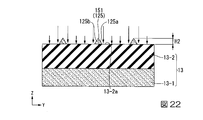
- the SOI substrate 13 includes a semiconductor substrate body 13-1, an insulating layer 13-2 covering one surface 13-1a of the semiconductor substrate body 13-1, and one surface of the insulating layer 13-2.
- the semiconductor layer 13-3 (SOI layer) covering the layer 13-2a is sequentially stacked.
- the semiconductor substrate body 13-1 is a substrate having a plate shape.
- As the semiconductor substrate body 13-1 for example, a p-type single crystal silicon substrate can be used.
- the insulating layer 13-2 is a buried insulating layer disposed between the semiconductor substrate body 13-1 and the semiconductor layer 13-3.
- the insulating layer 13-2 is disposed at a deep position from the main surface 13a of the SOI substrate 13 (in other words, the upper surface of the semiconductor layer 13-3) (for example, a position having a depth of 250 nm from the main surface 13a of the SOI substrate 13). ing.
- a silicon oxide film (SiO 2 film) called a buried oxide (BOX) film can be used as the insulating layer 13-2.
- the semiconductor layer 13-3 is a layer in which the first and second cell transistors 25 and 27 are formed.
- As the semiconductor layer 13-3 for example, a p-type single crystal silicon layer can be used.
- the thickness M1 of the semiconductor layer 13-3 can be set to, for example, 300 nm.
- a case where a p-type single crystal silicon layer is used as an example of the semiconductor layer 13-3 will be described.
- a plurality of first element isolation regions 14 are provided in the semiconductor layer 13-3 so as to extend in the X direction (second direction).
- the first element isolation region 14 extends in the X direction, and the first element isolation trench 14- provided in the semiconductor layer 13-3 so as to expose the one surface 13-2a of the insulating layer 13-2. 1 and a first element isolation insulating film 14-2 (for example, a silicon oxide film (SiO 2 film)) filling the first element isolation trench 14-1.
- a first element isolation insulating film 14-2 for example, a silicon oxide film (SiO 2 film) filling the first element isolation trench 14-1.
- the first element isolation region 14 has a depth reaching the one surface 13-2a of the insulating layer 13-2.
- the plurality of first element isolation regions 14 are arranged at predetermined intervals in the Y direction (first direction). Thus, the plurality of first element isolation regions 14 divide (divide) the semiconductor layer 13-3 into a plurality of parts in the Y direction.
- a plurality of second element isolation regions 17 are provided in the semiconductor layer 13-3 and the first element isolation region 14 so as to extend in the Y direction.
- the second element isolation region 17 divides the plurality of first element isolation regions 14 arranged in the Y direction.
- the second element isolation region 17 includes a second element isolation trench 17-1 and a second element isolation insulating film 17-2 (for example, a silicon oxide film (SiO 2 film)).
- the second element isolation trench 17-1 is provided in the semiconductor layer 13-3 and the first element isolation region 14 so as to extend in the Y direction and expose the one surface 13-2a of the insulating layer 13-2. It is done.
- the second element isolation insulating film 17-2 fills the second element isolation trench 17-1.
- the second element isolation region 17 has a depth reaching the one surface 13-2a of the insulating layer 13-2.
- a plurality of second element isolation regions 17 are arranged in the X direction.
- the plurality of second element isolation regions 17 divide (divide) the semiconductor layer 13-3 into a plurality of portions in the X direction.
- the active region 19 is composed of a semiconductor layer 13-3 partitioned by first and second element isolation regions 14 and 17.
- a plurality of active regions 19 are arranged so as to be aligned with respect to the X direction and the Y direction.
- the plurality of active regions 19 are insulated and isolated from the other active regions 19 arranged in the X and Y directions by the first and second element isolation regions 14 and 17.
- the active region 19 is a region that functions as an element formation layer in which the first and second cell transistors 25 and 27 are formed.
- the first and second grooves 21 and 22 are grooves extending in the Y direction, and are provided so as to straddle the plurality of active regions 19 and the first element isolation regions 14 arranged in the Y direction.
- One first and second grooves 21 and 22 are provided for each active region 19.
- the first trench 21 is a trench in which the first gate insulating film 59-1 and the first gate electrode 31 are disposed.
- the second trench 22 is a trench in which the second gate insulating film 59-2 and the second gate electrode 74 are disposed.
- the depth of the first and second grooves 21 and 22 (the depth when the main surface 13a of the SOI substrate 13 is used as a reference) is set to a depth that does not reach the one surface 13-2a of the insulating layer 13-2. .
- the depth of the first and second grooves 21 and 22 is such that the semiconductor layer 13 is located between the bottom surfaces 21a and 22a of the first and second grooves 21 and 22 and the one surface 13-2a of the insulating layer 13-2. -3 is the remaining thickness.
- the bottom surfaces 21a and 22a of the first and second grooves 21 and 22 are disposed so as to be close to the one surface 13-2a of the insulating layer 13-2.
- the semiconductor layer 13-3 is left between the bottom surface 21a of the first groove 21 and the one surface 13-2a of the insulating layer 13-2.
- the semiconductor layer 13-3 can function as a first bottom channel region 66 described later of the first cell transistor 25.
- the semiconductor layer 13-3 is left between the bottom surface 22a of the second groove 22 and the one surface 13-2a of the insulating layer 13-2. As a result, the semiconductor layer 13-3 can function as a second bottom channel region 77 described later of the second cell transistor 27.
- the depth of the first and second grooves 21 and 22 is increased.
- the thickness of the semiconductor layer 13-3 functioning as the first and second bottom channel regions 66 and 77 is reduced, and the first and second bottom channel regions 66 and 77 serving as charge paths are cut off. The area can be reduced.
- one first cell transistor 25 (selection transistor) is provided for each of the plurality of active regions 19.
- the first cell transistor 25 includes a first gate insulating film 59-1, a first gate electrode 61, a first sidewall channel region 63, a second sidewall channel region 64, a first A bottom channel region 66, a first capacitor impurity diffusion region 68, and a bit line impurity diffusion region 71 are provided.
- the first gate insulating film 59-1 is provided so as to cover the inner surface of the first trench 21.
- the first gate electrode 61 is provided so as to bury the lower portion of the first trench 21 via the first gate insulating film 59-1.
- a conductive material can be used as a material of the first gate electrode 61.
- a metal such as tungsten (W), polycrystalline silicon, or the like can be used.
- the first gate electrode 61 can be constituted by a laminated film in which, for example, a titanium nitride film (TiN film) and a tungsten film (W film) are sequentially laminated.
- TiN film titanium nitride film
- W film tungsten film
- the first side wall channel region 63 is constituted by the active region 19 (semiconductor layer 13-3).
- the active region 19 is formed between the second element isolation region 17 and the side surface 21 b (side surface intersecting with the X direction (orthogonal in the case of the first embodiment)) of the first groove 21. Located between.
- the second side wall channel region 64 is composed of the active region 19 (semiconductor layer 13-3).
- the active region 19 semiconductor layer 13-3 includes a side surface 21c of the first groove 21 (side surface facing the side surface 21b in the X direction) and a side surface 22b of the second groove 22 (crossing the X direction (first direction). In the case of the embodiment, it is located between the side surface orthogonal).
- the second side wall portion channel region 64 is a side wall portion channel region shared between the first and second cell transistors 25 and 27.
- FIG. 5 is a cross-sectional view of the memory cell portion of the semiconductor device shown in FIG. 1 in the BB line direction, and is an enlarged view of only the components arranged around the first bottom channel region. .
- FIG. 6 shows a first element isolation region, a second element isolation region, an active region, a first bottom channel region, and a second bottom channel that constitute the memory cell portion of the semiconductor device of the first embodiment. It is a top view for demonstrating the positional relationship of an area
- the first element isolation region 14, the second element isolation region 17, the active region 19, and the first bottom channel Only region 66 and second bottom channel region 77 are shown.
- the first bottom channel region 66 is constituted by the active region 19.
- the active region 19 is disposed between the bottom surface 21a of the first groove 21 and the one surface 13-2a of the insulating layer 13-2.
- the side surfaces 66 a and 66 b (two side surfaces) of the first bottom channel region 66 are disposed to face each other in the Y direction and are in contact with the first element isolation region 14. Further, the upper surface 66c of the first bottom channel region 66 is in contact with the first gate insulating film 59-1.
- the side surfaces 66 a and 66 b (two side surfaces) of the first bottom channel region 66 arranged to face each other in the Y direction are brought into contact with the first element isolation region 14. Yes. Further, in the first bottom channel region 66, the upper surface 66c of the first bottom channel region 66 is in contact with the first gate insulating film 59-1. Further, in the first bottom channel region 66, the lower surface 66d of the first bottom channel region 66 is in contact with the one surface 13-2a (upper surface) of the insulating layer 13-2.
- the cross-sectional area of the bottom channel region 66 can be reduced. Therefore, it is possible to limit the movement of floating electrons through the first bottom channel region 66, that is, the flow of floating electrons through the first bottom channel region 66. For this reason, a disturbance failure can be suppressed.
- the first bottom channel region 66 has ends 66A and 66B (two ends) arranged in the X direction.
- the end portion 66A (one end portion) is connected (integrated) with the first side wall portion channel region 63.
- the end portion 66B is connected (integrated) with the second side wall portion channel region 64.
- first sidewall channel region 63, the second sidewall channel region 64, and the first bottom channel region 66 are continuous from the first capacitor impurity diffusion region 68 to the bit line impurity diffusion region 71. To configure the channel.
- the first bottom channel region 66 is a flat channel region having an upper surface 66c and a lower surface 66d parallel to the one surface 13-1a of the semiconductor substrate body 13-1.
- the first bottom channel region 66 is a flat channel region having an upper surface 66c and a lower surface 66d parallel to the one surface 13-1a of the semiconductor substrate body 13-1. This makes it possible to limit the flow path of floating electrons that pass through the first bottom channel region 66, as compared to the configuration in which the flow path is not limited as in the prior art shown in FIG. Therefore, disturbance disturbance can be suppressed.
- the thickness M2 of the first bottom channel region 66 is less than 1/20 of the thickness M1 of the semiconductor layer 13-3. If it is thin, the cross-sectional area of the bottom channel region 66 becomes too small. For this reason, not only the movement of the floating electrons through the first bottom channel region 66 is restricted, but also the normal flow of electrons is restricted. Therefore, there arises a problem that the ON current is reduced.
- the thickness M2 of the first bottom channel region 66 is larger than 1/5 of the thickness M1 of the semiconductor layer 13-3, the cross-sectional area of the bottom channel region 66 is increased, so that the first bottom channel region 66 It becomes impossible to limit the movement of stray electrons via 66. Therefore, there arises a problem that disturb disturbance cannot be suppressed.
- the thickness M2 of the first bottom channel region 66 is preferably in the range of 1/20 to 1/5 of the thickness M1 of the semiconductor layer 13-3.
- the thickness M2 of the first bottom channel region 66 should be within a range of 1/15 to 1/10 of the thickness M1 of the semiconductor layer 13-3. As described above, by setting the thickness M2 of the first bottom channel region 66 within the range of 1/15 to 1/10 of the thickness M1 of the semiconductor layer 13-3, the disturb failure is more effectively suppressed. be able to.
- the thickness M2 of the first bottom channel region 66 may be set within a range of 20 to 30 nm, for example.
- the first bottom channel region 66 serving as a charge path is limited to a cross-sectional area defined by the width W1 ⁇ thickness M2 of the first bottom channel region due to the presence of the insulating layer 13-2 of the SOI substrate 13. Will be.
- the second bottom channel region 77 serving as a charge path is formed by a width W2 ⁇ thickness M3 of the second bottom channel region 77 due to the presence of the insulating layer 13-2 of the SOI substrate 13. It will be limited to the area.
- the first capacitor impurity diffusion region 68 is provided in the active region 19 located between the upper portion of the second element isolation region 17 and the upper portion of the first groove 21. ing. Thus, the first capacitor impurity diffusion region 68 is disposed on the first sidewall channel region 63.
- the first capacitor impurity diffusion region 68 functions as a source / drain region.
- the upper surface 68 a of the first capacitor impurity diffusion region 68 coincides with the main surface 13 a of the SOI substrate 13.
- the first capacitor impurity diffusion region 68 is a region formed by doping the active region 19 with an impurity (for example, an n-type impurity when the semiconductor layer 13-3 is a p-type semiconductor).
- the bit line impurity diffusion region 71 is provided in the active region 19 located between the upper part of the first groove 21 and the upper part of the second groove 22. As a result, the bit line impurity diffusion region 71 is disposed on the second sidewall channel region 64.
- the bit line impurity diffusion region 71 functions as a common source / drain region of the first and second cell transistors 25 and 27.
- the upper surface 71 a of the bit line impurity diffusion region 71 coincides with the main surface 13 a of the SOI substrate 13.
- the bit line impurity diffusion region 71 is a region formed by doping the active region 19 with an impurity (for example, an n-type impurity when the semiconductor layer 13-3 is a p-type semiconductor).
- One second cell transistor 27 (selection transistor) is provided for each of the plurality of active regions 19.
- the second cell transistor 27 includes a second gate insulating film 59-2, a second gate electrode 74, a second sidewall channel region 64, a third sidewall channel region 76, a second A bottom channel region 77, a bit line impurity diffusion region 71, and a second capacitor impurity diffusion region 78 are provided.
- the second gate insulating film 59-2 is configured in the same manner as the first gate insulating film 59-1 described above except that it is provided so as to cover the inner surface of the second trench 22. .
- the second gate electrode 74 is provided so as to embed the lower portion of the second trench 22 via the second gate insulating film 59-2.
- As the material of the second gate electrode 74 a material similar to the material of the first gate electrode 61 described above can be used.
- the third side wall channel region 76 has a side surface 22c (a side surface intersecting with the X direction (a side surface orthogonal to the first embodiment)) of the second groove 22 and the second side wall channel region 76.
- the active region 19 semiconductor layer 13-3) located between the two element isolation regions 17 is formed.
- the second bottom channel region 77 is composed of an active region 19 disposed between the bottom surface 22a of the second groove 22 and the one surface 13-2a of the insulating layer 13-2.
- the side surfaces 77 a and 77 b (two side surfaces) of the second bottom channel region 77 are disposed opposite to each other in the Y direction and are in contact with the first element isolation region 14.
- the upper surface 77c of the second bottom channel region 77 is in contact with the second gate insulating film 59-2.
- the second bottom channel region 77 has end portions 77A and 77B (two end portions) arranged in the X direction.
- the end 77A (one end) is connected (integrated) with the second side wall channel region 64.
- the end 77B is connected (integrated) with the third sidewall channel region 76.
- the second sidewall channel region 64, the third sidewall channel region 76, and the second bottom channel region 77 are continuous from the second capacitor impurity diffusion region 78 to the bit line impurity diffusion region 71. To configure the channel.
- the second bottom channel region 77 is a flat channel region having an upper surface 77c and a lower surface 77d parallel to the one surface 13-1a of the semiconductor substrate body 13-1.
- the thickness M3 of the second bottom channel region 77 is 1/20 to 1/2 of the thickness M1 of the semiconductor layer 13-3. It is preferable to set within the range of / 5, more preferably within the range of 1/15 to 1/10 of the thickness M1 of the semiconductor layer 13-3.
- the thickness M3 of the second bottom channel region 77 can be the same as the thickness M2 of the first bottom channel region 66, for example.
- the width W2 of the second bottom channel region 77 is configured to be equal to the width W1 of the first bottom channel region 66.
- the second capacitor impurity diffusion region 78 is provided in the active region 19 located between the upper portion of the second element isolation region 17 and the upper portion of the second groove 22. ing. Thus, the second capacitor impurity diffusion region 78 is disposed on the third sidewall channel region 76.
- the second capacitor impurity diffusion region 78 functions as a source / drain region.
- An upper surface 78 a of the second capacitor impurity diffusion region 78 coincides with the main surface 13 a of the SOI substrate 13.
- the second capacitor impurity diffusion region 78 is a region formed by doping the active region 19 with an impurity (for example, an n-type impurity when the semiconductor layer 13-3 is a p-type semiconductor).
- the first interlayer insulating film 29 is provided on the first and second element isolation regions 14 and 17.
- a silicon nitride film (SiN film) having a thickness of 20 nm can be used as the first interlayer insulating film 29, for example.
- the first interlayer insulating film 29 functions as an etching mask when the second element isolation trench 17-1 is formed in the semiconductor layer 13-3 by anisotropic dry etching by being patterned.
- the buried insulating film 32 is disposed so as to bury the upper portions of the first grooves 21 and 22. As a result, the upper surfaces of the first and second gate electrodes 61 and 74 are covered with the buried insulating film 32.
- the upper surface of the buried insulating film 32 is flush with the upper surface of the first interlayer insulating film 29.
- a silicon oxide film SiO 2 film
- the bit line contact opening 33 is provided on the bit line impurity diffusion region 71 and exposes the upper surface 71 a of the bit line impurity diffusion region 71.
- the bit line contact opening 33 is an opening formed by removing the first interlayer insulating film 29 located on the bit line impurity diffusion region 71 by anisotropic dry etching.
- the bit line contact plug 35 is provided so as to fill the bit line contact opening 33. Thus, the lower end of the bit line contact plug 35 is in contact with the upper surface 71 a of the bit line impurity diffusion region 71.
- the bit line contact plug 35 can be made of, for example, a polysilicon film.
- the bit line 37 is provided on the first interlayer insulating film 29.
- the lower end of the bit line 37 is integrated with the bit line contact plug 35. Thereby, the bit line 37 is electrically connected to the bit line impurity diffusion region 71 via the bit line contact plug 35.
- the shape of the bit line 37 is a snake pattern.
- the snake pattern includes a third direction (V direction) forming an angle ⁇ with the X direction and an angle ⁇ with the X direction so as to be connected to the upper ends of the bit line contact plugs 35 aligned in the X direction. And a meandering pattern along the X direction above the first element isolation region 14 and alternately having a slope of the fourth direction (W direction).
- the film constituting the bit line 37 for example, a laminated film in which a titanium nitride film and a tungsten film are sequentially laminated, a titanium nitride film, or the like can be used.
- the cap insulating film 39 is provided so as to cover the upper surface of the bit line 37.
- the cap insulating film 39 protects the upper surface of the bit line 37 and functions as an etching mask when patterning a base material that becomes the bit line 37 by anisotropic etching (specifically, dry etching).
- the cap insulating film 39 for example, a silicon nitride film (SiN film) can be used.
- the first sidewall film 41 is provided so as to cover the side surface of the bit line 37 and the side surface of the cap insulating film 39.
- the second sidewall film 42 is provided so as to cover the outer wall surface of the first sidewall film 41.
- a silicon nitride film SiN film
- SiN film silicon nitride film
- the second interlayer insulating film 44 is provided on the first interlayer insulating film 29 so as to fill the space between the bit lines 37 via the first and second sidewall films 41 and 42.
- the upper surface of the second interlayer insulating film 44 is set to the upper surface of the cap insulating film 39.
- the second interlayer insulating film 44 for example, a silicon oxide film (SiO 2 film) formed by a CVD (Chemical Vapor Deposition) method, or a coating type insulating film formed by an SOG (Spin On Glass) method (Silicon oxide film (SiO 2 film)) or the like can be used.
- a silicon oxide film (SiO 2 film) formed by a CVD (Chemical Vapor Deposition) method or a coating type insulating film formed by an SOG (Spin On Glass) method (Silicon oxide film (SiO 2 film)) or the like
- SOG Spin On Glass
- the first capacitor contact hole 45-1 exposes the first interlayer insulating film 29, the buried insulating film 32, and the second interlayer insulating film 44 so as to expose the upper surface 68 a of the first capacitor impurity diffusion region 68. Is formed.
- the second capacitor contact hole 45-2 exposes the first interlayer insulating film 29, the buried insulating film 32, and the second interlayer insulating film 44 so as to expose the upper surface 78a of the second capacitor impurity diffusion region 78. Is formed.
- the first capacitor contact plug 46-1 is provided so as to embed the first capacitor contact hole 45-1.
- the lower end of the first capacitor contact plug 46-1 is in contact with the upper surface 68a of the first capacitor impurity diffusion region 68.
- the first capacitor contact plug 46-1 is electrically connected to the first capacitor impurity diffusion region 68.
- the upper surface of the first capacitor contact plug 46-1 is flush with the upper surface of the second interlayer insulating film 44.
- the first capacitor contact plug 46-1 can have, for example, a laminated structure in which a titanium nitride film and a tungsten film are sequentially laminated.
- the second capacitor contact plug 46-2 is provided so as to fill the second capacitor contact hole 45-2.
- the lower end of the second capacitor contact plug 46-2 is in contact with the upper surface 78a of the second capacitor impurity diffusion region 78.
- the second capacitor contact plug 46-2 is electrically connected to the second capacitor impurity diffusion region 78.
- the upper surface of the second capacitor contact plug 46-2 is flush with the upper surface of the second interlayer insulating film 44.
- the second capacitor contact plug 46-2 can have a stacked structure in which, for example, a titanium nitride film and a tungsten film are sequentially stacked.
- the stopper film 48 is provided on the upper surface of the cap insulating film 39 and the upper surface of the second interlayer insulating film 44.
- the stopper film 48 has a function of protecting elements (for example, the first and second cell transistors 25 and 27) arranged in the lower layer.
- the stopper film 48 for example, a silicon nitride film (SiN film) can be used.
- the third interlayer insulating film 49 is provided on the stopper film 48.
- a silicon oxide film SiO 2 film
- the cylinder hole 51 is provided so as to penetrate the stopper film 48 and the third interlayer insulating film 49 located on the first capacitor contact plug 46-1 and the second capacitor contact plug 46-2. .
- the cylinder hole 51 disposed on the first capacitor contact plug 46-1 exposes the upper surface of the first capacitor contact plug 46-1.
- the cylinder hole 51 disposed on the second capacitor contact plug 46-2 exposes the upper surface of the second capacitor contact plug 46-2.
- One capacitor 53 is provided for each of the first and second capacitive contact plugs 46-1 and 46-2.
- One capacitor 53 includes one lower electrode 84, a capacitive insulating film 85 common to the plurality of lower electrodes 84, and an upper electrode 86 that is a common electrode to the plurality of lower electrodes 84.
- the lower electrode 84 has a crown shape and is provided on the first and second capacitor contact plugs 46-1 and 46-2, respectively.
- the lower electrode 84 disposed on the first capacitor contact plug 46-1 is electrically connected to the first capacitor impurity diffusion region 68 via the first capacitor contact plug 46-1. ing.
- the lower electrode 84 disposed on the second capacitor contact plug 46-2 is electrically connected to the second capacitor impurity diffusion region 78 via the second capacitor contact plug 46-2. Yes.
- the capacitor insulating film 85 is disposed so as to cover the surface of the lower electrode 84 and the upper surface of the third interlayer insulating film 49.
- the capacity insulating film 85 has a thickness that does not fill the cylinder hole 51.
- the upper electrode 86 is provided so as to cover the surface of the capacitive insulating film 85.
- the upper electrode 86 is disposed so as to bury the inside of the lower electrode 84 in which the capacitive insulating film 85 is formed.
- the upper surface of the upper electrode 86 is disposed above the upper ends of the plurality of lower electrodes 84.
- one cell includes one cell transistor (the first cell transistor 25 or the second cell transistor 27) and one capacitor 53. Therefore, two cells are provided in one active region 19. Specifically, the two cells are a cell composed of the first cell transistor 25 and the capacitor 53 and a cell composed of the second cell transistor 27 and the capacitor 53.
- the fourth interlayer insulating film 55 is provided so as to cover the upper surface of the upper electrode film 86.
- a silicon oxide film SiO 2 film
- a via penetrating the fourth interlayer insulating film 55 and having the lower end connected to the upper electrode 86 may be provided. Further, a wiring (not shown) connected to the upper end of the via may be provided on the fourth interlayer insulating film 55.
- the protective film 57 is provided on the fourth interlayer insulating film 55.
- the protective film 57 has a function of protecting the wiring when a wiring (not shown) is provided on the fourth interlayer insulating film 55.
- the semiconductor device includes a first cell transistor 25 and a second cell transistor 27.
- the first cell transistor 25 includes a first sidewall channel region 63 constituted by an active region 19 located between the first trench 21 and the second element isolation region 17, and a first sidewall channel.
- a first side wall channel region 64 composed of a first capacitor impurity diffusion region 68 disposed on the region 63, an active region 19 located between the first and second trenches 21, 22,
- the second cell transistor 27 includes a third sidewall channel region 76 constituted by an active region 19 located between the second trench 22 and the second element isolation region 17, and a third sidewall channel.
- the second cell transistor 27 is provided in the same active region 19 as the first cell transistor 25.
- the semiconductor layer 13-3 (in other words, disposed between the bottom surface of the first and second grooves 21 and 22 and the insulating layer)
- the thickness of the first and second bottom channel regions 66, 77) is reduced. Therefore, it is possible to reduce the cross-sectional areas of the first and second bottom channel regions 66 and 77 serving as charge paths.
- the passage of electric charges is restricted by the first and second bottom channel regions 66 and 77.
- the probability of electrons reaching the capacitor contact plug (the first capacitor contact plug 46-1 or the second capacitor contact plug 46-2) of the adjacent cell can be reduced to about 1/10 to 1/100. it can.
- the first cell transistor 25 Repeat on / off.
- the second capacitor contact plug 46-2 electrically connected to the second cell transistor 27 is set to “High” and the second cell transistor 27 is held off.
- the first cell transistor 25 Repeat on / off.
- the second bottom channel region located below the second trench 22 of the second cell transistor 27 even if floating electrons are generated in the active region 19 located below the bit line impurity diffusion region 71, the second bottom channel region located below the second trench 22 of the second cell transistor 27.
- the small cross-sectional area of 77 is an obstacle. Therefore, the probability that electric charge can circulate becomes extremely small.
- the semiconductor device 10 according to the first embodiment can suppress a disturb failure between two cells arranged in the same active region 19.
- the first and second cell transistors are operated during the operation of the first transistor.
- the second bottom channel regions 66 and 77 can be completely depleted.
- the first and second cell transistors 25 and 27 have a fully depleted channel structure, the first and second cell transistors 25 and 25 formed by the first and second gate electrodes 61 and 74 are provided. 27 threshold control characteristics can be improved.
- FIG. 7 is an enlarged cross-sectional view of a portion different from the semiconductor device of the first embodiment in the memory cell portion of the semiconductor device according to the modification of the first embodiment of the present invention.
- FIG. 7 corresponds to the cut surface of FIG. In FIG. 7, the same components as those of the structure shown in FIG.
- the semiconductor device 95 according to the modification of the first embodiment is arranged such that the first gate insulating film 59-1 covers the side surfaces 66a and 66b of the first bottom channel region 66. Is done.
- the side surfaces 66a and 66b of the first bottom channel region 66 and the first gate electrode 61 are arranged to face each other via the first gate insulating film 59-1.
- the second gate insulating film 59-2 is disposed so as to cover the side surfaces 77a and 77b of the second bottom channel region 77.
- the side surfaces 77a and 77b of the second bottom channel region 77 and the second gate electrode 74 are arranged to face each other via the second gate insulating film 59-2.
- the semiconductor device 95 according to the modification of the first embodiment is configured in the same manner as the semiconductor device 10 except that the configuration described above is different from the semiconductor device 10 of the first embodiment.
- the semiconductor device 95 having the saddle fin structure can obtain the same effects as those of the semiconductor device 10 of the first embodiment.
- FIG. 8 to 14 are diagrams showing manufacturing steps of the semiconductor device according to the first embodiment of the present invention. Specifically, FIG. 8 is a cross-sectional view for explaining a manufacturing process of the SOI substrate.
- FIG. 9A is a plan view showing a memory cell portion of a semiconductor device being manufactured.
- 9B is a cross-sectional view of the structure shown in FIG. 9A in the direction of the AA line.
- FIG. 10 and 11 are cross-sectional views showing the memory cell portion of the semiconductor device being manufactured.
- FIG. 12A is a plan view showing a memory cell portion of a semiconductor device being manufactured.
- 12B is a cross-sectional view of the structure shown in FIG. 12A in the direction of the AA line.
- 13 and 14 are cross-sectional views showing the memory cell portion of the semiconductor device being manufactured.
- a semiconductor substrate for example, a p-type single crystal silicon wafer
- Oxygen is implanted by ion implantation from a main surface of the semiconductor substrate (main surface 13a of the SOI substrate 13) to a predetermined depth (for example, 250 to 350 nm).
- the semiconductor substrate is heated to form an insulating layer 13-2 (in this case, a silicon oxide film (SiO 2 film)).
- the semiconductor substrate body 13-1 made of the semiconductor substrate located below the insulating layer 13-2, the insulating layer 13-2, and the semiconductor layer made of the semiconductor substrate located above the insulating layer 13-2.
- the SOI substrate 13 in which 13-3 are sequentially stacked is formed.
- the thickness M1 of the semiconductor layer 13-3 can be set to, for example, 300 nm.
- the thickness M4 of the insulating layer 13-2 can be set to 10 nm, for example.
- a well-known commercially available SOI substrate may be used.
- the semiconductor substrate body 13-1 and the semiconductor layer 13-3 are made of p-type single crystal silicon will be described as an example.
- a known technique for example, STI (Shallow trench isolation) method
- STI shallow trench isolation
- a first element isolation region 14 is formed.
- a plurality of first element isolation regions 14 are formed in the Y direction.
- the plurality of first element isolation regions 14 are formed so that the upper surfaces thereof are flush with the main surface 13 a of the SOI substrate 13.
- the first element isolation region 14 extends in the Y direction of the SOI substrate 13 on which the first element isolation region 14 is formed, and is formed on the one surface 13-2a of the insulating layer 13-2.
- a second element isolation region 17-1 that reaches the second element isolation region 17-1 for example, a silicon oxide film (SiO 2 film)
- SiO 2 film silicon oxide film
- a plurality of second element isolation regions 17 are formed in the X direction.
- the plurality of second element isolation regions 17 are formed so that the upper surfaces thereof are flush with the main surface 13 a of the SOI substrate 13.
- the width W3 of the active region 19 in the Y direction can be set to 40 nm, for example.
- an n-type impurity is implanted into the upper surfaces 19a of the plurality of active regions 19 (main surface 13a of the SOI substrate 13) by ion implantation, thereby forming an impurity diffusion layer 98 on the plurality of active regions 19.
- the impurity diffusion layer 98 is divided into the first capacitor impurity diffusion region 68, the bit line impurity diffusion region 71, and the second capacitor impurity diffusion region 78 shown in FIG.
- the structure shown in FIGS. 9A and 9B (specifically, the upper surface of the first element isolation region 14, the upper surface of the second element isolation region 17, Then, a first interlayer insulating film 29 covering the upper surface 19a) of the active region 19 is formed.
- the first interlayer insulating film 29 made of the silicon nitride film (SiN film) is formed.
- the first and second opening grooves 29A, 29B is formed.
- the first opening groove 29 ⁇ / b> A is formed so as to correspond to the formation region of the first groove 21.
- the second opening groove 29 ⁇ / b> B is formed so as to correspond to the formation region of the second groove 22.
- the plurality of active regions 19 and the first element isolation regions 14 are formed by anisotropic dry etching using the first interlayer insulating film 29 in which the first and second opening grooves 29A and 29B are formed as an etching mask.
- first and second grooves 21 and 22 having a depth that does not reach the one surface 13-2a of the insulating layer 13-2 are formed.
- the first capacitance impurity diffusion region 68 disposed between the side surface 21 b of the first groove 21 and the second element isolation region 17, the first groove 21, and the second groove 22 A bit line impurity diffusion region 71 disposed therebetween, a second capacitor impurity diffusion region 78 disposed between the side surface 22c of the second trench 22 and the second element isolation region 17, and a first First sidewall channel region 63 disposed between capacitor impurity diffusion region 68 and insulating layer 13-2, and disposed between bit line impurity diffusion region 71 and insulating layer 13-2.
- the thicknesses M2 and M3 of the first and second bottom channel regions 66 and 77 are equal to the thickness of the semiconductor layer 13-3. It is formed to be within a range of 1/20 to 1/5 of M1.
- the first and second trenches 21 and 22 are such that the thicknesses M2 and M3 of the first and second bottom channel regions 66 and 77 are 1/15 to 1 to the thickness M1 of the semiconductor layer 13-3. It is good to form so that it may become in the range of / 10.
- the first and second trenches 21 and 22 are, for example, the thickness M2 of the first and second bottom channel regions 66 and 77. It is preferable to form M3 within a range of 20 to 30 nm.
- the first bottom channel region 66 formed by the above method is a flat channel region having an upper surface 66c and a lower surface 66d parallel to one surface 13-1a of the semiconductor substrate body 13-1.
- An end portion 66 ⁇ / b> A arranged in the X direction is connected (integrated) with the first side wall portion channel region 63.
- An end 66B arranged in the X direction is connected (integrated) with the second side wall channel region 64.
- the second bottom channel region 77 formed by the above method is a flat channel region having an upper surface 77c and a lower surface 77d parallel to the one surface 13-1a of the semiconductor substrate body 13-1.
- the end 77A arranged in the X direction is connected (integrated) with the second side wall channel region 64.
- the end portion 77B arranged in the X direction is connected (integrated) with the side wall channel region 76 of the third rib.
- a first gate insulating film 59-1 (in this case, a silicon oxide film (SiO 2 film)) covering the inner surface of the first trench 21 and a second gate are formed by a known method (for example, thermal oxidation method).
- a second gate insulating film 59-2 (in this case, a silicon oxide film (SiO 2 film)) covering the inner surface of the trench 22 is formed in a lump.
- the first gate electrode 61 filling the lower portion of the first trench 21 via the first gate insulating film 59-1, and the second gate insulating film 59-2.
- a second gate electrode 74 that fills the lower portion of the second trench 22 is collectively formed.
- the conductive film Is etched back, so that the first and second gate electrodes 61 and 74 are collectively formed.
- the first cell transistor 25 includes a first gate insulating film 59-1, a first gate electrode 61, a first sidewall channel region 63, a second sidewall channel region 64, and a first bottom channel region 66.
- the first capacitor impurity diffusion region 68 and the bit line impurity diffusion region 71 are provided.
- the second cell transistor 27 includes a second gate insulating film 59-2, a second gate electrode 74, a second sidewall channel region 64, a third sidewall channel region 76, and a second bottom channel region 77.
- a bit line impurity diffusion region 71 and a second capacitor impurity diffusion region 78 is provided for one active region 19.
- the first cell transistor 25 includes a first gate insulating film 59-1, a first gate electrode 61, a first sidewall channel region 63, a second sidewall channel region 64, and a first bottom channel region 66.
- the first capacitor impurity diffusion region 68 and the bit line impurity diffusion region 71 are provided.
- a buried insulating film 32 that fills the upper portions of the first and second grooves 21 and 22 is formed by a known method. At this time, the buried insulating film 32 is formed so that the upper surface thereof is flush with the upper surface of the first interlayer insulating film 29.
- the first interlayer insulating film 29 located on the bit line impurity diffusion region 71 is removed by a photolithography technique and a dry etching technique, thereby exposing the upper surface 71a of the bit line impurity diffusion region 71.
- a contact opening 33 is formed.
- bit line contact plug 35 that fills the bit line contact opening 33 and has the lower end connected to the upper surface 71a of the bit line impurity diffusion region 71 is formed by a well-known method.
- bit line contact plug 35 is formed so that the upper surface thereof is flush with the upper surface of the buried insulating film 32 and the upper surface of the first interlayer insulating film 29.
- the conductive film constituting the bit line contact plug 35 for example, a laminated film in which a titanium nitride (TiN) film and a tungsten (W) film are sequentially laminated can be used.
- TiN titanium nitride
- W tungsten
- a metal film 101 for example, a titanium nitride film (TiN film) and a tungsten film (W film) covering the upper surface of the structure shown in FIG. 11 is sequentially stacked. Film) and the silicon nitride film 102 are sequentially stacked.
- the cap insulating film 39 made of the silicon nitride film 102 is formed by patterning the silicon nitride film 102 by a photolithography technique and a dry etching technique. At this time, the cap insulating film 39 is formed to have a snake pattern.
- the metal film 101 is patterned by anisotropic dry etching using the cap insulating film 39 as a mask, whereby the bit line 37 made of the metal film 101 is formed with a snake pattern.
- bit line 37 The lower end of the bit line 37 is connected to the bit line contact plug 35. Thereby, the bit line 37 is electrically connected to the bit line impurity diffusion region 71 via the bit line contact plug 35.
- a first sidewall film 41 and a second sidewall film 42 that cover the side surface of the cap insulating film 39 and the side surface of the bit line 37 are sequentially formed by a well-known method.
- the interlayer insulating film 44 is formed.
- the second interlayer insulating film 44 is formed so that the upper surface thereof is flush with the upper surface of the cap insulating film 39.
- the first and second interlayer insulating films 29 and 44 located on the first capacitor impurity diffusion region 68 and the second capacitor impurity diffusion region 78 are formed by a self-aligned contact method (SAC method).
- SAC method self-aligned contact method
- the first capacitor contact plug 46-1 having the first capacitor contact hole 45-1 buried therein and the lower end connected to the first capacitor impurity diffusion region 68, and the second capacitor A second capacitor contact plug 46-2 that fills the contact hole 45-2 and is connected to the second capacitor impurity diffusion region 78 is collectively formed.
- the first and second capacitor contact plugs 46-1 and 46-2 are formed so that the upper surfaces thereof are flush with the upper surface of the second interlayer insulating film 44.
- a stopper film 48 is formed on the structure shown in FIG. 13 by a known method.
- the stopper film 48 is formed by, for example, forming a silicon nitride film (SiN film).
- a third interlayer insulating film 49 is formed on the stopper film 48 by a known method.
- the third interlayer insulating film 49 is formed, for example, by forming a silicon oxide film (SiO 2 film).
- the stopper film 48 and the third interlayer insulating film 49 located on the first capacitor contact plug 46-1 and the second capacitor contact plug 46-2 are removed by photolithography technique and dry etching technique. As a result, the cylinder hole 51 exposing the upper surface of the first capacitor contact plug 46-1 or the upper surface of the second capacitor contact plug 46-2 is formed.
- the lower electrode 84 that covers the inner surface of the cylinder hole 51 is formed by a known method.
- the lower electrode 84 having a crown shape is disposed on the first and second capacitor contact plugs 46-1 and 46-2.
- a capacitor insulating film 85 that continuously covers the inner surfaces of the plurality of lower electrodes 84 and the upper surface of the third interlayer insulating film 49 is formed by a known method.
- an upper electrode 86 having a flat upper surface embedded in the plurality of lower electrodes 84 and disposed above the capacitor insulating film 85 is formed through the capacitor insulating film 85.
- one capacitor 53 (a capacitor composed of the lower electrode 84, the capacitor insulating film 85, and the upper electrode 86) is provided for each of the plurality of first and second capacitor contact plugs 46-1 and 46-2. Is formed.
- one active region 19 includes two cells (specifically, a cell composed of the first cell transistor 25 and the capacitor 53, a second cell transistor 27, A cell formed of the capacitor 53 is formed.
- a fourth interlayer insulating film 55 (for example, a silicon oxide film (SiO 2 film)) covering the upper surface of the upper electrode film 86 is formed by a known method.
- a via that penetrates through the fourth interlayer insulating film 55 and has a lower end connected to the upper electrode 86 may be formed. Further, a wiring (not shown) connected to the upper end of the via may be formed on the fourth interlayer insulating film 55.
- a protective film 57 is formed on the fourth interlayer insulating film 55, whereby the memory cell portion 11 of the semiconductor device 10 of the first embodiment is manufactured.
- FIG. 15 is an isometric view illustrating the main part of the memory cell portion of the semiconductor device of the second embodiment by isometric projection.
- FIG. 16 is an enlarged cross-sectional view of the memory cell portion surrounded by the region B shown in FIG.
- a DRAM is taken as an example as an example of the semiconductor device 110 according to the second embodiment.
- the same components as those of the semiconductor device 10 of the first embodiment are denoted by the same reference numerals.
- the semiconductor device 110 according to the second embodiment includes a first groove 21, a second groove 22, and a first groove constituting the semiconductor device 10 according to the first embodiment.
- the semiconductor device 10 except that it has a first groove 113, a second groove 114, a first cell transistor 116, and a second cell transistor 117 in place of the cell transistor 25 and the second cell transistor 27. It is configured in the same way.
- the first groove 113 has the same configuration as the first groove 21 described in the first embodiment except that the bottom surface 113a has a flat portion and a raised portion.
- the second groove 114 has the same configuration as the second groove 22 described in the first embodiment except that the bottom surface 114a has a flat portion and a raised portion.
- the first cell transistor 116 has a first bottom channel region 121 in place of the first bottom channel region 66 constituting the first cell transistor 25 described in the first embodiment.
- the configuration is the same as that of the first cell transistor 25.
- the first bottom channel region 121 has the same configuration as the second bottom channel region 122 shown in FIG. 16 except that the arrangement position thereof is different from that of the second bottom channel region 122.
- the first bottom channel region 121 is disposed between the bottom surface 121a of the first groove 121 and the insulating layer 13-2, and has a flat channel region 124 and a protruding channel region 125.
- the flat channel region 124 has an upper surface 124c and a lower surface 124d parallel to the one surface 13-1a of the semiconductor substrate body 13-1.
- the side surfaces 124 a and 124 b of the flat channel region 124 arranged to face each other in the Y direction are in contact with the first element isolation region 14. Further, the upper surface 124c of the flat channel region 124 is in contact with the first gate insulating film 59-1.
- the lower surface 124d of the flat channel region 124 is in contact with the one surface 13-2a of the insulating layer 13-2.
- one end is integrated with the first side wall channel region 63.
- the other end is integrated with the second side wall channel region 64.
- the thickness M5 of the flat channel region 124 configured as described above can be set to, for example, 25 nm.
- the protruding channel region 125 is a channel region protruding upward from the upper surface 124 c of the flat channel region 124, and is integrated with the flat channel region 124.
- the protruding channel region 125 has two inclined side surfaces 125a and 125b, and the shape of the cut surface is a triangle.
- the protruding amount H1 of the protruding channel region 125 when the upper surface 124c of the flat channel region 124 is used as a reference can be, for example, 25 nm.
- the second cell transistor 117 has a second bottom channel region 122 in place of the second bottom channel region 77 constituting the second cell transistor 27 described in the first embodiment.
- the configuration is the same as that of the second cell transistor 27.
- the second bottom channel region 122 is disposed between the bottom surface 122a of the second groove 122 and the insulating layer 13-2, and ends in the X direction are the second side wall channel region 64 and the third side wall.
- the configuration is the same as that of the first bottom channel region 121 described above except that it is integrated with the partial channel region 76.
- the second bottom channel region 122 has a flat channel region 124 and a protruding channel region 125.
- the semiconductor device 110 of the second embodiment configured as described above can obtain the same effects as the semiconductor device 10 of the first embodiment.
- first and second bottom channel regions 121 and 122 are maintained fully depleted, and the cross-sectional area is increased as compared with the first and second bottom channels 66 and 77 described in the first embodiment. It becomes possible to make it. Therefore, it is possible to increase Ion and improve the S characteristics when the first and second cell transistors 116 and 117 are operated.
- S characteristic is a common name in the industry for a subthreshold coefficient (S factor), and means a gate voltage required to change the drain current value by one digit. Therefore, the smaller the gate voltage, the more effectively the on / off control of the transistor can be achieved, which contributes to higher speed operation and lower power consumption.
- S factor subthreshold coefficient
- FIG. 17 is an enlarged cross-sectional view of a portion different from the semiconductor device of the second embodiment in the memory cell portion of the semiconductor device according to the modification of the second embodiment of the present invention.
- the same components as those of the structure shown in FIG. 17 are identical components as those of the structure shown in FIG. 17
- the side surfaces 124a and 124b of the flat channel region 124 are covered with the first gate insulating film 59-1 (not shown in FIG. 17) or the second gate insulating film 59-2. Yes.
- the side surfaces 124a and 124b of the planar channel region 124 are connected to the first gate electrode 61 (not shown in FIG. 17) or the first gate insulating film 59-1 or the second gate insulating film 59-2.
- the semiconductor device 130 according to the modified example of the second embodiment is configured similarly to the semiconductor device 110 of the second embodiment.
- the semiconductor device 130 having the saddle fin structure can obtain the same effects as those of the semiconductor device 10 of the first embodiment. Further, the semiconductor device 130 maintains the fully depleted first and second bottom channel regions 121 and 122, and the first and second bottom channels 66 and 77 described in the first embodiment. Also, the cross-sectional area can be increased. Therefore, the semiconductor device 130 can increase Ion and improve the S characteristic when the first and second cell transistors 116 and 117 are operated.
- 18 and 19 are cross-sectional views showing the steps of the semiconductor device according to the second embodiment of the present invention. 18 and 19, the same components as those shown in FIGS. 15 and 16 are denoted by the same reference numerals.
- FIGS. 9A and 9B is formed by sequentially performing the process shown in FIG. 8 described in the first embodiment and the process shown in FIGS. 9A and 9B.
- a step of forming the first interlayer insulating film 29 having the first and second opening grooves 29A and 29B is performed.
- the anisotropic process is performed using an etching condition in which the etching selectivity of the first element isolation region 14 is larger than that of the semiconductor layer 13-3 (for example, an etching condition with a selectivity of about 3 to 10).
- the semiconductor layer 13-3 and the first element isolation region 14 are etched through the first interlayer insulating film 29 having the first and second opening grooves 29A and 29B by the characteristic dry etching.
- the first element isolation region 14 is etched faster than the semiconductor layer 13-3.
- the upper surface of the first element isolation region 14 is disposed below the upper surface of the semiconductor layer 13-3, and the semiconductor layer 13-3 separated from the first element isolation region 14 is provided.
- a protruding portion having a mountain shape protruding upward is formed in the central portion.
- the first element isolation region 14 and the semiconductor layer 13-3 corresponding to the formation region of the second trench 114 are formed in the first element isolation shown in FIG.
- the region 14 and the semiconductor layer 13-3 are etched into the same shape.
- etching conditions for example, the selection ratio is about 3 to 10 having high anisotropy and a higher selection ratio of the semiconductor layer 13-3 than the first element isolation region 14 are used.
- the first and second opening grooves 29A and 29B (not shown in FIG. 19) are formed under the condition that the shape of the protruding portion remains at the upper end of the semiconductor layer 13-3 by anisotropic etching.
- the semiconductor layer 13-3 and the first element isolation region 14 that are located are etched.
- first and second bottom channel regions 121 and 122 (the second bottom channel region 122 is not shown in FIG. 19) including the flat channel region 124 and the protruding channel region 125 are collectively formed.
- the anisotropic etching is preferably performed so that the height H1 of the top of the protruding channel region 125 with respect to the upper surface of the first element isolation region 14 after etching is 50 nm or less.
- the memory cell unit 111 of the semiconductor device 110 of the second embodiment shown in FIG. 15 is manufactured.
- FIG. 20 is an isometric view illustrating the main part of the memory cell portion of the semiconductor device of the third embodiment by isometric projection.
- FIG. 21 is an enlarged cross-sectional view of the memory cell portion surrounded by the region C shown in FIG.
- a DRAM is taken as an example as an example of the semiconductor device 140 of the third embodiment.
- the same components as those of the semiconductor devices 10 and 110 of the first and second embodiments described above are denoted by the same reference numerals.
- the semiconductor device 140 according to the third embodiment includes a first groove 21, a second groove 22, and a first groove constituting the semiconductor device 10 according to the first embodiment.
- the first groove 143 has a portion where the bottom surface 143a is flat and a raised portion, and the first groove 143 is exposed to a part of the one surface 13-2a of the insulating layer 13-2.
- the configuration is the same as that of the first groove 21 described in the embodiment.
- the second groove 144 has a portion where the bottom surface 144a is flat and a raised portion, and the second groove 144 is exposed in a part of the one surface 13-2a of the insulating layer 13-2.
- the configuration is the same as that of the second groove 22 described in the embodiment.
- the first cell transistor 146 has a first bottom channel region 151 instead of the first bottom channel region 66 constituting the first cell transistor 25 described in the first embodiment.
- the configuration is the same as that of the first cell transistor 25.
- the first bottom channel region 151 has the same configuration as the second bottom channel region 152 shown in FIG. 21 except that the arrangement position thereof is different from that of the second bottom channel region 152.
- the first bottom channel region 151 has the same configuration as the protruding channel region 125 having the two inclined side surfaces 125a and 125b described in the second embodiment and the cut surface having a triangular shape. It is said that.
- the height H2 of the first bottom channel region 151 with respect to the one surface 13-2a of the insulating layer 13-2 can be appropriately selected within a range of 25 nm to 50 nm, for example.
- the second cell transistor 147 has a second bottom channel region 152 in place of the second bottom channel region 77 constituting the second cell transistor 27 described in the first embodiment.
- the configuration is the same as that of the second cell transistor 27.
- the second bottom channel region 152 has the same shape as the first bottom channel region 151 described above (see FIG. 21).
- the semiconductor device of the third embodiment has a first bottom channel region 151 and a second bottom channel region 152.
- the first bottom channel region 151 has two inclined side surfaces 125a and 125b, the cut surface has a triangular shape, and is integrated with the first and second side wall channel regions 63 and 64.
- the second bottom channel region 152 has two inclined side surfaces 125a and 125b, the cut surface has a triangular shape, and is integrated with the second and third side wall channel regions 64 and 76.
- the first and second cross-sectional areas of the first and second bottom channel regions 66 and 77 described in the semiconductor device 10 of the first embodiment are larger. It becomes possible to reduce the cross-sectional areas of the bottom channel regions 151 and 152. Therefore, the semiconductor device according to the third embodiment can more effectively suppress disturb failures than the semiconductor device 10.
- FIG. 22 is a cross-sectional view showing a process of the semiconductor device according to the third embodiment of the present invention. 22, the same components as those shown in FIGS. 20 and 21 are denoted by the same reference numerals.
- FIGS. 9A and 9B is formed by sequentially performing the process shown in FIG. 8 described in the first embodiment and the process shown in FIGS. 9A and 9B.
- a step of forming the first interlayer insulating film 29 having the first and second opening grooves 29A and 29B is performed.
- FIG. 18 is formed by performing the same process as the process shown in FIG. 18 described in the second embodiment.
- first bottom channel region 151 having two inclined side surfaces 125a and 125b and the cut surface having a triangular shape and the two inclined side surfaces 125a and 125b having the shape of the cut surface.
- a second bottom channel region 152 (not shown in FIG. 22) having a triangular shape is collectively formed.
- the memory cell portion 141 of the semiconductor device 140 of the third embodiment shown in FIG. 20 is manufactured by performing the same process as the steps shown in FIGS. 11 to 14 described in the first embodiment.
- the present invention is applicable to semiconductor devices.
- First capacitor impurity diffusion region 71... Bit line impurity diffusion region, 74... Second gate electrode, 76... Third side wall channel region, 77, 122, 152. ... Second capacitor impurity diffusion region, 84. Lower electrode, 85. Capacitor insulating film, 86. Upper electrode, 98... Impurity diffusion layer, 101... Metal film, 102. , 125 ... projecting cha Nel region, H1 ... projection amount, H2 ... height, M1, M2, M3, M4 ... thickness, W1, W2, W3 ... width
Landscapes
- Semiconductor Memories (AREA)
Abstract
Description
本発明は、半導体装置に関する。 The present invention relates to a semiconductor device.
近年、半導体装置(半導体素子)の微細化に伴って、トランジスタの寸法も縮小化される傾向にある。この寸法の縮小により、トランジスタ(Tr)の短チャネル効果がより顕著になってきている。 In recent years, with the miniaturization of semiconductor devices (semiconductor elements), the size of transistors tends to be reduced. Due to the reduction in size, the short channel effect of the transistor (Tr) has become more prominent.
例えば、半導体装置のうちの1つであるDRAM(Dynamic Random Access Memory)では、メモリセルの寸法の縮小化によって、トランジスタのチャネル長も縮小される。このため、トランジスタのパフォーマンスが低下する。したがって、メモリセルのリテンションあるいは書き込み特性の悪化等が問題となってきている。 For example, in a DRAM (Dynamic Random Access Memory) which is one of semiconductor devices, the channel length of a transistor is also reduced by reducing the size of a memory cell. For this reason, the performance of the transistor decreases. Therefore, the retention of memory cells or the deterioration of write characteristics has become a problem.
このような問題を解決するために、半導体基板に溝(トレンチ)を形成することによってチャネルを3次元構造としたトレンチ(リセス)型FET(Field Effect Transistor)、あるいは、溝の間にフィンを形成することによってチャネルを3次元構造としたフィン型FET等が開発されている(例えば、特開2005-064500号公報(特許文献1)、特開2007-027753号公報(特許文献2)および特開2007-305827号公報(特許文献3)を参照)。 In order to solve such problems, a trench (recess) type FET (Field Effect Transistor) having a three-dimensional channel structure by forming a groove (trench) in a semiconductor substrate, or a fin between the grooves is formed. As a result, fin-type FETs having a three-dimensional channel have been developed (for example, Japanese Patent Application Laid-Open No. 2005-064500 (Patent Document 1), Japanese Patent Application Laid-Open No. 2007-027753 (Patent Document 2), and Japanese Patent Application Laid-Open No. 2007-027753. (See 2007-305827 (Patent Document 3)).
上記トレンチ型FETは、半導体基板に溝を形成し、該溝内にゲート絶縁膜を介してゲート電極を配置することで、チャネルを3次元構造としたトランジスタである。 The trench type FET is a transistor having a three-dimensional channel structure by forming a groove in a semiconductor substrate and disposing a gate electrode in the groove via a gate insulating film.
一方、フィン型FETは、半導体基板に形成された溝の間から突き出したフィンを跨ぐようにゲート絶縁膜を介してゲート電極を配置することで、チャネルを3次元構造としたトランジスタである。 On the other hand, a fin-type FET is a transistor having a three-dimensional channel structure by disposing a gate electrode through a gate insulating film so as to straddle a fin protruding from between grooves formed in a semiconductor substrate.
上記トレンチ型FET及びフィン型FETでは、チャネル幅に対してゲート長を長くすることが可能となる。このため、短チャネル効果を抑制することができる。 In the trench FET and the fin FET, the gate length can be increased with respect to the channel width. For this reason, the short channel effect can be suppressed.
また、DRAMでは、メモリセルの寸法の縮小化に伴って、該メモリセルを構成する選択用トランジスタとして、半導体基板の主面側に埋め込まれた埋め込み型ゲート電極を有するトランジスタを採用することも検討されている。 In addition, in DRAM, as the size of the memory cell is reduced, it is also considered to adopt a transistor having an embedded gate electrode embedded on the main surface side of the semiconductor substrate as a selection transistor constituting the memory cell. Has been.
このような構成とされたトランジスタでは、ゲート電極(ワード線)が半導体基板の主面側に埋め込まれている。このため、半導体基板の主面よりも上方にゲート電極が突き出すことがない。 In the transistor having such a configuration, the gate electrode (word line) is embedded in the main surface side of the semiconductor substrate. For this reason, the gate electrode does not protrude above the main surface of the semiconductor substrate.
また、メモリセルと接続される配線のうち半導体基板の上方に位置するのはビット線だけとなる。したがって、半導体基板上にメモリセルを構成するコンデンサおよびコンタクトプラグ等を形成する際の配置が容易となるだけでなく、その加工の困難さを軽減できるメリットがある。 Also, only the bit lines are located above the semiconductor substrate among the wirings connected to the memory cells. Therefore, there is an advantage that not only the arrangement when forming the capacitor, the contact plug, etc. constituting the memory cell on the semiconductor substrate is facilitated, but also the difficulty of the processing can be reduced.
上述した、埋め込み型ゲート電極を有するトランジスタ(Tr)では、半導体基板の主面側に埋め込まれたゲート電極(ワード線)の材料として、例えば、金属膜(ポリシリコン膜と比較して抵抗の低い膜)であるタングステン膜(W膜)及び窒化チタン膜(TiN膜)が用いられる。金属膜を用いることによって、ゲート電極(ワード線)及びビット線の容量の低減、GIDL(Gate-Induced-Drain-Leakage current)と呼ばれる電流の抑制、リテンション(Retention)特性の改善、および消費電流の低減等の効果が得られることがわかっている。 In the above-described transistor (Tr) having a buried gate electrode, as a material of the gate electrode (word line) buried on the main surface side of the semiconductor substrate, for example, a metal film (having a lower resistance than a polysilicon film) A tungsten film (W film) and a titanium nitride film (TiN film). By using a metal film, the capacitance of the gate electrode (word line) and the bit line is reduced, the current called GIDL (Gate-Induced-Drain-Leakage current) is suppressed, the retention characteristic is improved, and the consumption current is reduced. It has been found that effects such as reduction can be obtained.
しかしながら、微細化によってワード線の間隔が縮小されると、後述する図23で説明するように、同一活性領域内で隣接するメモリセル同士の動作が干渉するディスターブ不良が発生してしまう。 However, when the interval between the word lines is reduced by miniaturization, a disturb failure occurs in which the operations of adjacent memory cells interfere in the same active region, as will be described later with reference to FIG.
図23は、ディスターブ不良を説明するための従来の半導体装置のメモリセル部の主要部を模式的に示す断面図である。なお、図23では、第1及び第2のゲート電極223,228と交差するビット線212を模式的に図示する。
FIG. 23 is a cross-sectional view schematically showing a main part of a memory cell portion of a conventional semiconductor device for explaining a disturb failure. In FIG. 23, the
図23を参照するに、従来の半導体装置200は、半導体基板201と、素子分離領域202と、活性領域204と、第1のトランジスタ206と、第2のトランジスタ207と、ビット線コンタクトプラグ211と、ビット線212と、第1の容量コンタクトプラグ214(ストレージノードコンタクトプラグ)と、第2の容量コンタクトプラグ215(ストレージノードコンタクトプラグ)と、を有する。
Referring to FIG. 23, a
素子分離領域202は、半導体基板201の主面201a側に設けられており、活性領域204を区画している。活性領域204には、第1及び第2の溝201A,201Bが形成されている。
The
第1のトランジスタ206は、第1の溝201Aの内面を覆うゲート絶縁膜222と、ゲート絶縁膜222を介して、第1の溝201Aの下部を埋め込む第1のゲート電極223と、第1の溝201Aの上部と素子分離領域202との間に位置する活性領域204に形成された第1の不純物拡散領域225と、第1及び第2の溝201A,201Bの上部間に位置する活性領域204に形成された第2の不純物拡散領域226と、を有する。
The
第2のトランジスタ207は、第2の溝201Bの内面を覆うゲート絶縁膜222と、ゲート絶縁膜222を介して、第2の溝201Bの下部を埋め込む第2のゲート電極228と、第2の溝201Bの上部と素子分離領域202との間に位置する活性領域204に形成された第1の不純物拡散領域227と、第2の不純物拡散領域226(第1のトランジスタ206と共通の不純物拡散領域)と、を有する。
The
第2のトランジスタ207は、第1のトランジスタ206が設けられた活性領域204に設けられたトランジスタである。
The
ビット線コンタクトプラグ211は、第2の不純物拡散領域226の上面226aに設けられている。ビット線212は、ビット線コンタクトプラグ211上に設けられており、ビット線コンタクトプラグ211の上端と一体とされている。
The bit
第1の容量コンタクトプラグ214は、第1のトランジスタ206を構成する第1の不純物拡散領域225の上面225aと接続されている。
The first
第2の容量コンタクトプラグ215は、第2のトランジスタ207を構成する第1の不純物拡散領域227の上面227aと接続されている。
The second
上記構成とされた半導体装置200において、第2の容量コンタクトプラグ215を「High」にすると共に、第2のトランジスタ207をoff(オフ)状態とする。この状態で、第1のトランジスタ206のon-off(オンオフ)動作を繰り返し行うと、第1のトランジスタ206のチャネル領域231に励起され、かつ捕獲されないで浮遊状態となった電子(図23に示す「e-」)が第2のトランジスタ207の周囲を浮遊する。電子は、ある確率で第2の容量コンタクトプラグ215に侵入する。
In the
その結果、第2の容量コンタクトプラグ215に保持されている「High」情報が「Low」情報に破壊されるというディスターブ不良が発生する。
As a result, a disturb failure occurs in which “High” information held in the second
上記ディスターブ不良は、半導体装置の微細化に伴って、より深刻な問題となる。 The above disturb failure becomes a more serious problem as the semiconductor device is miniaturized.
本発明の一観点によれば、半導体基板本体、該半導体基板本体の一面を覆う絶縁層、及び該絶縁層の一面を覆う半導体層を含むSOI(Silicon on Insulator)基板と、前記半導体層を第1の方向に対して複数に分断する複数の第1の素子分離領域と、前記半導体層を前記第1の方向に対して交差する第2の方向に対して複数に分断する複数の第2の素子分離領域と、前記複数の第1及び第2の素子分離領域により区画されると共に、前記第1及び第2の方向において絶縁分離された複数の活性領域と、前記複数の活性領域のそれぞれに対して設けられ、前記第1の方向に延在すると共に、前記絶縁層に到達しない深さとされた2つの溝と、前記溝の内面を覆うゲート絶縁膜を介して、前記溝内に配置されたゲート電極を含み、同一の前記活性領域に配置された2つのトランジスタと、を備え、前記2つのトランジスタは、前記活性領域のうち、前記第2の方向において対向配置された前記溝の2つの側面を構成する部分に配置された側壁部チャネル領域と、前記活性領域のうち、前記溝の底面と前記絶縁層との間に位置する部分に配置された底部チャネル領域と、をそれぞれ有する半導体装置が提供される。 According to one aspect of the present invention, an SOI (Silicon on Insulator) substrate including a semiconductor substrate body, an insulating layer covering one surface of the semiconductor substrate body, and a semiconductor layer covering one surface of the insulating layer; A plurality of first element isolation regions that are divided into a plurality of parts in one direction, and a plurality of second element parts that are divided into a plurality of parts in a second direction that intersects the first direction. A plurality of active regions partitioned by an element isolation region and the plurality of first and second element isolation regions and insulated and isolated in the first and second directions, and each of the plurality of active regions The groove is disposed in the groove via two grooves extending in the first direction and having a depth that does not reach the insulating layer, and a gate insulating film covering the inner surface of the groove. Gate power And two transistors disposed in the same active region, and the two transistors constitute two side surfaces of the trench disposed opposite to each other in the second direction in the active region And a bottom channel region disposed in a portion of the active region located between the bottom surface of the trench and the insulating layer, respectively. The
本発明の一観点による半導体装置によれば、同一の活性領域に設けられた2つのトランジスタが、活性領域のうち、第2の方向において対向配置された溝の2つの側面を構成する部分に配置された側壁部チャネル領域と、活性領域のうち、溝の底面と絶縁層との間に位置する部分に配置された底部チャネル領域と、を有する。溝の深さを深くすることで、溝の底面と絶縁層との間に配置される半導体層の厚さを薄くして、電荷の通路となる底部チャネル領域の断面積を小さくすることが可能となる。 According to the semiconductor device of one aspect of the present invention, two transistors provided in the same active region are arranged in a portion of the active region that constitutes two side surfaces of the groove opposed to each other in the second direction. And a bottom channel region disposed in a portion of the active region located between the bottom surface of the trench and the insulating layer. By increasing the depth of the groove, it is possible to reduce the thickness of the semiconductor layer disposed between the bottom surface of the groove and the insulating layer, and to reduce the cross-sectional area of the bottom channel region serving as a charge path It becomes.
これにより、底部チャネル領域を経由する浮遊電子の移動(言い換えれば、底部チャネル領域を経由する浮遊電子の流通)を制限することが可能となる。したがってディスターブ不良を抑制することができる。 This makes it possible to limit the movement of floating electrons via the bottom channel region (in other words, the flow of floating electrons via the bottom channel region). Therefore, disturb failure can be suppressed.
以下、図面を参照して本発明を適用した実施の形態について詳細に説明する。なお、以下の説明で用いる図面は、特徴をわかりやすくするために、説明の便宜上、特徴となる部分を拡大して示している場合があり、各構成要素の寸法比率等が実際と同じであるとは限らない。 Hereinafter, an embodiment to which the present invention is applied will be described in detail with reference to the drawings. In addition, in the drawings used in the following description, in order to make the characteristics easy to understand, for convenience of description, the characteristic portions may be shown in an enlarged manner, and the dimensional ratios and the like of the respective components are the same as the actual ones. Not necessarily.
また、以下の説明において例示される材料、寸法等は一例であって、本発明はそれらに必ずしも限定されるものではなく、その要旨を変更しない範囲で適宜変更して実施することが可能である。 In addition, the materials, dimensions, and the like exemplified in the following description are merely examples, and the present invention is not necessarily limited thereto, and can be appropriately modified and implemented without departing from the scope of the invention. .
(第1の実施の形態)
図1は、本発明の第1の実施の形態に係る半導体装置を構成するメモリセル部の一部を拡大した平面図であり、メモリセル部の構成要素のうち、第1の素子分離領域、第2の素子分離領域、活性領域、第1の溝、第2の溝、第1のゲート電極、第2のゲート電極、ビット線コンタクトプラグ、及びビット線のみ図示した図である。
(First embodiment)
FIG. 1 is an enlarged plan view of a part of the memory cell portion constituting the semiconductor device according to the first embodiment of the present invention. Among the components of the memory cell portion, the first element isolation region, FIG. 5 is a diagram illustrating only a second element isolation region, an active region, a first groove, a second groove, a first gate electrode, a second gate electrode, a bit line contact plug, and a bit line.
図2は、図1に示す半導体装置のメモリセル部のA-A線方向の断面図である。図3は、図2に示すメモリセル部のうち、領域Aに囲まれた部分を拡大した断面図である。図4は、アイソメトリック図法により、第1の実施の形態の半導体装置のメモリセル部の主要部を図示した等角投影図である。 FIG. 2 is a cross-sectional view taken along the line AA of the memory cell portion of the semiconductor device shown in FIG. FIG. 3 is an enlarged cross-sectional view of a portion surrounded by the region A in the memory cell portion shown in FIG. FIG. 4 is an isometric view illustrating the main part of the memory cell portion of the semiconductor device of the first embodiment by isometric projection.
図1~図4では、第1の実施の形態の半導体装置10の一例として、DRAM(Dynamic Random Access Memory)を例に挙げて図示する。
FIGS. 1 to 4 illustrate a DRAM (Dynamic Random Access Memory) as an example of the
図1~図4において、X方向(第2の方向)は、第1の素子分離領域14の延在方向を示している。Y方向(第1の方向)は、X方向と交差(図1の場合、直交)する第2の素子分離領域17の延在方向を示している。Z方向は、X方向及びY方向に対して直交する方向(言い換えれば、半導体基板本体13-1の厚さ方向)を示している。
1 to 4, the X direction (second direction) indicates the extending direction of the first
図1において、W1は、図3に示し、かつ図1に図示していない第1の底部チャネル領域66のY方向の幅(以下、「幅W1」という)を示している。W2は、図3に示し、かつ図1に図示していない第2の底部チャネル領域77のY方向の幅(以下、「幅W2」という)を示している。なお、幅W1,W2は、Y方向における活性領域19の幅と等しい。
1, W1 represents the width in the Y direction (hereinafter referred to as “width W1”) of the first
また、図2及び図4では、ビット線37を模式的に図示する。ビット線37は、実際には、図1に示すようにX方向に延在する。
2 and 4, the
図1~図4において、同一構成部分には、同一符号を付す。
図1~図4を参照するに、第1の実施の形態の半導体装置10は、メモリセル領域に設けられたメモリセル部11と、メモリセル部11の周囲に位置する周辺回路領域(図示せず)に設けられた周辺回路部(図示せず)と、を有する。
1 to 4, the same components are denoted by the same reference numerals.
1 to 4, a
メモリセル部11には、複数のメモリセル(セル)がマトリックス状に並んで配置されている。一方、周辺回路部(図示せず)には、各メモリセルの動作を制御するための回路(図示していない周辺回路用トランジスタも含む)が配置されている。
In the
以下、主に、第1の実施の形態の半導体装置10を構成するメモリセル部11の構成について説明する。
Hereinafter, the configuration of the
第1の実施の形態の半導体装置10のメモリセル部11は、SOI(Silicon on Insulator)基板13と、第1の素子分離領域14と、第2の素子分離領域17と、活性領域19と、第1の溝21と、第2の溝22と、第1のセルトランジスタ25(第1のトランジスタ)と、第2のセルトランジスタ27(第2のトランジスタ)と、第1の層間絶縁膜29と、埋め込み絶縁膜32と、ビット線コンタクト開口部33と、ビット線コンタクトプラグ35と、ビット線37と、キャップ絶縁膜39と、第1のサイドウォール膜41と、第2のサイドウォール膜42と、第2の層間絶縁膜44と、第1の容量コンタクト孔45-1と、第2の容量コンタクト孔45-2と、第1の容量コンタクトプラグ46-1と、第2の容量コンタクトプラグ46-2と、ストッパー膜48と、第3の層間絶縁膜49と、シリンダ孔51と、キャパシタ53と、第4の層間絶縁膜55と、保護膜57と、を有する。
The
図2及び図4を参照するに、SOI基板13は、半導体基板本体13-1と、半導体基板本体13-1の一面13-1aを覆う絶縁層13-2と、絶縁層13-2の一面13-2aを覆う半導体層13-3(SOI層)と、が順次積層された構成とされている。
2 and 4, the
半導体基板本体13-1は、板状とされた基板である。半導体基板本体13-1としては、例えば、p型単結晶シリコン基板を用いることができる。 The semiconductor substrate body 13-1 is a substrate having a plate shape. As the semiconductor substrate body 13-1, for example, a p-type single crystal silicon substrate can be used.
絶縁層13-2は、半導体基板本体13-1と半導体層13-3との間に配置された埋め込み絶縁層である。絶縁層13-2は、SOI基板13の主面13a(言い換えれば、半導体層13-3の上面)から深い位置(例えば、SOI基板13の主面13aから250nmの深さの位置)に配置されている。
The insulating layer 13-2 is a buried insulating layer disposed between the semiconductor substrate body 13-1 and the semiconductor layer 13-3. The insulating layer 13-2 is disposed at a deep position from the
絶縁層13-2としては、例えば、埋め込み酸化(BOX;Buried Oxide)膜と呼ばれるシリコン酸化膜(SiO2膜)を用いることができる。 As the insulating layer 13-2, for example, a silicon oxide film (SiO 2 film) called a buried oxide (BOX) film can be used.
半導体層13-3は、第1及び第2のセルトランジスタ25,27が形成される層である。半導体層13-3としては、例えば、p型の単結晶シリコン層を用いることができる。
The semiconductor layer 13-3 is a layer in which the first and
この場合、半導体層13-3の厚さM1は、例えば、300nmとすることができる。
なお、以下の説明では、半導体層13-3の一例として、p型の単結晶シリコン層を用いた場合を例に挙げて説明する。
In this case, the thickness M1 of the semiconductor layer 13-3 can be set to, for example, 300 nm.
In the following description, a case where a p-type single crystal silicon layer is used as an example of the semiconductor layer 13-3 will be described.
図1及び図4を参照するに、第1の素子分離領域14は、X方向(第2の方向)に延在するように、半導体層13-3に複数設けられている。
1 and 4, a plurality of first
第1の素子分離領域14は、X方向に延在し、かつ絶縁層13-2の一面13-2aを露出するように半導体層13-3に設けられた第1の素子分離用溝14-1と、第1の素子分離用溝14-1を埋め込む第1の素子分離用絶縁膜14-2(例えば、シリコン酸化膜(SiO2膜))と、を有する。
The first
これにより、第1の素子分離領域14は、絶縁層13-2の一面13-2aに到達する深さとされている。
Thereby, the first
複数の第1の素子分離領域14は、Y方向(第1の方向)に所定の間隔で配置されている。これにより、複数の第1の素子分離領域14は、半導体層13-3をY方向に対して複数に分断(分割)している。
The plurality of first
第2の素子分離領域17は、Y方向に延在するように、半導体層13-3及び第1の素子分離領域14に複数設けられている。第2の素子分離領域17は、Y方向に配置された複数の第1の素子分離領域14を分断している。
A plurality of second
第2の素子分離領域17は、第2の素子分離用溝17-1と、第2の素子分離用絶縁膜17-2(例えば、シリコン酸化膜(SiO2膜))と、を有する。第2の素子分離用溝17-1は、Y方向に延在し、かつ絶縁層13-2の一面13-2aを露出するように半導体層13-3及び第1の素子分離領域14に設けられる。第2の素子分離用絶縁膜17-2は、第2の素子分離用溝17-1を埋め込む。
The second
これにより、第2の素子分離領域17は、絶縁層13-2の一面13-2aに到達する深さとされている。
Thereby, the second
複数の第2の素子分離領域17は、X方向に対して複数配置されている。これにより、複数の第2の素子分離領域17は、半導体層13-3をX方向に対して複数に分断(分割)している。
図1~図3を参照するに、活性領域19は、第1及び第2の素子分離領域14,17で区画された半導体層13-3で構成されている。活性領域19は、X方向及びY方向に対して整列するように複数配置されている。複数の活性領域19は、第1及び第2の素子分離領域14,17により、X方向及びY方向において周囲に配置された他の活性領域19とは絶縁分離されている。
A plurality of second
Referring to FIGS. 1 to 3, the
活性領域19は、第1及び第2のセルトランジスタ25,27が形成される素子形成層として機能する領域である。
The
第1及び第2の溝21,22は、Y方向に延在する溝であり、Y方向に配置された複数の活性領域19及び第1の素子分離領域14に跨るように設けられている。第1及び第2の溝21,22は、1つの活性領域19に対して、それぞれ1つ設けられている。
The first and
第1の溝21は、第1のゲート絶縁膜59-1及び第1のゲート電極31が配置される溝である。第2の溝22は、第2のゲート絶縁膜59-2及び第2のゲート電極74が配置される溝である。
The
第1及び第2の溝21,22の深さ(SOI基板13の主面13aを基準としたときの深さ)は、絶縁層13-2の一面13-2aに到達しない深さとされている。つまり、第1及び第2の溝21,22の深さは、第1及び第2の溝21,22の底面21a,22aと絶縁層13-2の一面13-2aとの間に半導体層13-3が残存する厚さとされている。第1及び第2の溝21,22の底面21a,22aは、絶縁層13-2の一面13-2aに近接するように配置されている。
The depth of the first and
このように、第1の溝21の底面21aと絶縁層13-2の一面13-2aとの間に半導体層13-3を残存させる。これにより、該半導体層13-3を、第1のセルトランジスタ25の後述する第1の底部チャネル領域66として機能させることが可能になる。
Thus, the semiconductor layer 13-3 is left between the
また、第2の溝22の底面22aと絶縁層13-2の一面13-2aとの間に半導体層13-3を残存させる。これにより、該半導体層13-3を第2のセルトランジスタ27の後述する第2の底部チャネル領域77として機能させることが可能になる。
Further, the semiconductor layer 13-3 is left between the
また、第1及び第2の溝21,22の深さを深くする。これにより、第1及び第2の底部チャネル領域66,77として機能する半導体層13-3の厚さを薄くして、電荷の通路となる第1及び第2の底部チャネル領域66,77の断面積を小さくすることが可能となる。
Also, the depth of the first and
したがって、第1及び第2の底部チャネル領域66,77を経由する浮遊電子(e-)の移動(言い換えれば、第1及び第2の底部チャネル領域66,77を経由する浮遊電子の流通)を制限することが可能となるので、ディスターブ不良を抑制できる。
Therefore, the movement of floating electrons (e − ) via the first and second
図2~図4を参照するに、第1のセルトランジスタ25(選択トランジスタ)は、複数の活性領域19に対してそれぞれ1つ設けられている。
2 to 4, one first cell transistor 25 (selection transistor) is provided for each of the plurality of
第1のセルトランジスタ25は、第1のゲート絶縁膜59-1と、第1のゲート電極61と、第1の側壁部チャネル領域63と、第2の側壁部チャネル領域64と、第1の底部チャネル領域66と、第1の容量用不純物拡散領域68と、ビット線用不純物拡散領域71と、を有する。
The
第1のゲート絶縁膜59-1は、第1の溝21の内面を覆うように設けられている。第1のゲート絶縁膜59-1としては、例えば、単層のシリコン酸化膜(SiO2膜)、シリコン酸化膜を窒化した膜(SiON膜)、積層されたシリコン酸化膜(SiO2膜)、シリコン酸化膜(SiO2膜)上にシリコン窒化膜(SiN膜)を積層させた積層膜等を用いることができる。
The first gate insulating film 59-1 is provided so as to cover the inner surface of the
第1のゲート電極61は、第1のゲート絶縁膜59-1を介して、第1の溝21の下部を埋め込むように設けられている。第1のゲート電極61の材料としては、導電材料を用いることができる。該導電材料としては、例えば、タングステン(W)等の金属、あるいは多結晶シリコン等を用いることができる。
The
具体的には、第1のゲート電極61は、例えば、窒化チタン膜(TiN膜)と、タングステン膜(W膜)と、を順次積層した積層膜で構成することができる。
Specifically, the
図3及び図4を参照するに、第1の側壁部チャネル領域63は、活性領域19(半導体層13-3)により構成されている。活性領域19(半導体層13-3)は、第1の溝21の側面21b(X方向と交差(第1の実施の形態の場合、直交)する側面)と第2の素子分離領域17との間に位置する。
3 and 4, the first side
第2の側壁部チャネル領域64は、活性領域19(半導体層13-3)により構成されている。活性領域19(半導体層13-3)は、第1の溝21の側面21c(X方向において側面21bと対向する側面)と、第2の溝22の側面22b(X方向と交差(第1の実施の形態の場合、直交)する側面)と、の間に位置する。
The second side
第2の側壁部チャネル領域64は、第1及び第2のセルトランジスタ25,27間で共有される側壁部チャネル領域である。
The second side wall
図5は、図1に示す半導体装置のメモリセル部のB-B線方向の断面図であり、第1の底部チャネル領域の周囲に配置された構成要素のみを拡大して図示した図である。 FIG. 5 is a cross-sectional view of the memory cell portion of the semiconductor device shown in FIG. 1 in the BB line direction, and is an enlarged view of only the components arranged around the first bottom channel region. .
図6は、第1の実施の形態の半導体装置のメモリセル部を構成する第1の素子分離領域、第2の素子分離領域、活性領域、第1の底部チャネル領域、及び第2の底部チャネル領域の位置関係を説明するための平面図である。図6では、第1の実施の形態の半導体装置10のメモリセル部11の構成要素のうち、第1の素子分離領域14、第2の素子分離領域17、活性領域19、第1の底部チャネル領域66、及び第2の底部チャネル領域77のみを図示する。
FIG. 6 shows a first element isolation region, a second element isolation region, an active region, a first bottom channel region, and a second bottom channel that constitute the memory cell portion of the semiconductor device of the first embodiment. It is a top view for demonstrating the positional relationship of an area | region. In FIG. 6, among the components of the
なお、図5及び図6において、図1~図4に示す構造体と同一構成部分には同一符号を付す。 5 and 6, the same components as those shown in FIGS. 1 to 4 are denoted by the same reference numerals.
次に、図3~図6を参照して、第1の底部チャネル領域66について説明する。
第1の底部チャネル領域66は、活性領域19により構成されている。活性領域19は、第1の溝21の底面21aと絶縁層13-2の一面13-2aとの間に配置される。
Next, the first
The first
第1の底部チャネル領域66の側面66a,66b(2つの側面)は、Y方向において対向配置されるとともに、第1の素子分離領域14と接触している。また、第1の底部チャネル領域66の上面66cは、第1のゲート絶縁膜59-1と接触している。
The side surfaces 66 a and 66 b (two side surfaces) of the first
このように、第1の底部チャネル領域66では、Y方向において対向配置された第1の底部チャネル領域66の側面66a,66b(2つの側面)を第1の素子分離領域14と接触させる構成としている。さらに、第1の底部チャネル領域66では、第1の底部チャネル領域66の上面66cを第1のゲート絶縁膜59-1と接触させる構成としている。さらに、第1の底部チャネル領域66では、第1の底部チャネル領域66の下面66dを、絶縁層13-2の一面13-2a(上面)と接触させる構成としている。
As described above, in the first
これにより、底部チャネル領域66の断面積を狭くすることができる。したがって、第1の底部チャネル領域66を経由する浮遊電子の移動、すなわち、第1の底部チャネル領域66を経由する浮遊電子の流通を制限することが可能となる。このため、ディスターブ不良を抑制できる。
Thereby, the cross-sectional area of the
第1の底部チャネル領域66は、X方向に配置された端部66A,66B(2つの端部)を有する。端部66A(一方の端部)は、第1の側壁部チャネル領域63と接続(一体化)されている。端部66Bは、第2の側壁部チャネル領域64と接続(一体化)されている。
The first
これにより、第1の側壁部チャネル領域63、第2の側壁部チャネル領域64、及び第1の底部チャネル領域66は、第1の容量用不純物拡散領域68からビット線用不純物拡散領域71まで連続するチャネルを構成している。
Thus, the first
第1の底部チャネル領域66は、半導体基板本体13-1の一面13-1aに平行な上面66c及び下面66dを有した平板状チャネル領域である。
The first
このように、第1の底部チャネル領域66を、半導体基板本体13-1の一面13-1aに平行な上面66c及び下面66dを有した平板状チャネル領域とする。これにより、図23に示した従来技術のように流通経路が制限されない構成に比べて、第1の底部チャネル領域66を経由する浮遊電子の流通経路を制限することが可能となる。したがってディスターブ不良を抑制できる。
Thus, the first
第1の底部チャネル領域66の厚さM2(半導体基板本体13-1の一面13-1aに対して直交する方向における厚さ)が、半導体層13-3の厚さM1の1/20よりも薄いと、底部チャネル領域66の断面積が小さくなりすぎる。このため、第1の底部チャネル領域66を経由する浮遊電子の移動を制限するだけでなく、正常な電子の流れまで制限されてしまう。したがって、ON電流が低下するという問題が発生する。
The thickness M2 of the first bottom channel region 66 (thickness in the direction orthogonal to the one surface 13-1a of the semiconductor substrate body 13-1) is less than 1/20 of the thickness M1 of the semiconductor layer 13-3. If it is thin, the cross-sectional area of the
また、第1の底部チャネル領域66の厚さM2が半導体層13-3の厚さM1の1/5よりも厚いと、底部チャネル領域66の断面積が大きくなるので、第1の底部チャネル領域66を経由する浮遊電子の移動を制限することができなくなる。したがってディスターブ不良を抑制できないという問題が発生してしまう。
Further, if the thickness M2 of the first
上記理由により、第1の底部チャネル領域66の厚さM2は、半導体層13-3の厚さM1の1/20~1/5の範囲内にするとよい。
For the above reason, the thickness M2 of the first
また、好ましくは、第1の底部チャネル領域66の厚さM2は、半導体層13-3の厚さM1の1/15~1/10の範囲内にするとよい。このように、第1の底部チャネル領域66の厚さM2を半導体層13-3の厚さM1の1/15~1/10の範囲内にすることで、より効果的にディスターブ不良を抑制することができる。
Also preferably, the thickness M2 of the first
具体的には、半導体層13-3の厚さM1が300nmの場合、第1の底部チャネル領域66の厚さM2は、例えば、20~30nmの範囲内に設定するとよい。
Specifically, when the thickness M1 of the semiconductor layer 13-3 is 300 nm, the thickness M2 of the first
電荷の通路となる第1の底部チャネル領域66は、SOI基板13の絶縁層13-2が存在することにより、第1の底部チャネル領域の幅W1×厚さM2で規定される断面積に制限されることになる。
The first
また、電荷の通路となる第2の底部チャネル領域77は、SOI基板13の絶縁層13-2が存在することにより、第2の底部チャネル領域77の幅W2×厚さM3で規定される断面積に制限されることになる。
In addition, the second
図2~図4を参照するに、第1の容量用不純物拡散領域68は、第2の素子分離領域17の上部と第1の溝21の上部との間に位置する活性領域19に設けられている。これにより、第1の容量用不純物拡散領域68は、第1の側壁部チャネル領域63上に配置されている。
2 to 4, the first capacitor
第1の容量用不純物拡散領域68は、ソース/ドレイン領域として機能する。第1の容量用不純物拡散領域68の上面68aは、SOI基板13の主面13aと一致している。
The first capacitor
第1の容量用不純物拡散領域68は、活性領域19に不純物(例えば、半導体層13-3がp型半導体の場合、n型不純物)をドープすることで形成される領域である。
The first capacitor
ビット線用不純物拡散領域71は、第1の溝21の上部と第2の溝22の上部との間に位置する活性領域19に設けられている。これにより、ビット線用不純物拡散領域71は、第2の側壁部チャネル領域64上に配置されている。
The bit line
ビット線用不純物拡散領域71は、第1及び第2のセルトランジスタ25,27の共通のソース/ドレイン領域として機能する。ビット線用不純物拡散領域71の上面71aは、SOI基板13の主面13aと一致している。
The bit line
ビット線用不純物拡散領域71は、活性領域19に不純物(例えば、半導体層13-3がp型半導体の場合、n型不純物)をドープすることで形成される領域である。
The bit line
第2のセルトランジスタ27(選択トランジスタ)は、複数の活性領域19に対してそれぞれ1つ設けられている。
One second cell transistor 27 (selection transistor) is provided for each of the plurality of
第2のセルトランジスタ27は、第2のゲート絶縁膜59-2と、第2のゲート電極74と、第2の側壁部チャネル領域64と、第3の側壁部チャネル領域76と、第2の底部チャネル領域77と、ビット線用不純物拡散領域71と、第2の容量用不純物拡散領域78と、を有する。
The
第2のゲート絶縁膜59-2は、第2の溝22の内面を覆うように設けられていること以外は、先に説明した第1のゲート絶縁膜59-1と同様に構成されている。
The second gate insulating film 59-2 is configured in the same manner as the first gate insulating film 59-1 described above except that it is provided so as to cover the inner surface of the
第2のゲート電極74は、第2のゲート絶縁膜59-2を介して、第2の溝22の下部を埋め込むように設けられている。第2のゲート電極74の材料としては、先に説明した第1のゲート電極61の材料と同様な材料を用いることができる。
The
図3及び図4を参照するに、第3の側壁部チャネル領域76は、第2の溝22の側面22c(X方向と交差(第1の実施の形態の場合、直交)する側面)と第2の素子分離領域17との間に位置する活性領域19(半導体層13-3)により構成されている。
Referring to FIGS. 3 and 4, the third side
次に、図3、図4、及び図6を参照して、第2の底部チャネル領域77について説明する。
Next, the second
第2の底部チャネル領域77は、第2の溝22の底面22aと絶縁層13-2の一面13-2aとの間に配置された活性領域19により構成されている。
The second
第2の底部チャネル領域77の側面77a,77b(2つの側面)は、Y方向において対向配置されるとともに、第1の素子分離領域14と接触している。また、第2の底部チャネル領域77の上面77cは、第2のゲート絶縁膜59-2と接触している。
The side surfaces 77 a and 77 b (two side surfaces) of the second
第2の底部チャネル領域77は、X方向に配置された端部77A,77B(2つの端部)を有する。端部77A(一方の端部)は、第2の側壁部チャネル領域64と接続(一体化)されている。端部77Bは、第3の側壁部チャネル領域76と接続(一体化)されている。
The second
これにより、第2の側壁部チャネル領域64、第3の側壁部チャネル領域76、及び第2の底部チャネル領域77は、第2の容量用不純物拡散領域78からビット線用不純物拡散領域71まで連続するチャネルを構成している。
As a result, the second
第2の底部チャネル領域77は、半導体基板本体13-1の一面13-1aに平行な上面77c及び下面77dを有した平板状チャネル領域である。
The second
第2の底部チャネル領域77の厚さM3(半導体基板本体13-1の一面13-1aに対して直交する方向における厚さ)は、半導体層13-3の厚さM1の 1/20~1/5の範囲内で設定することが好ましく、より好ましくは、半導体層13-3の厚さM1の1/15~1/10の範囲内で適宜設定するとよい。 The thickness M3 of the second bottom channel region 77 (thickness in the direction perpendicular to the one surface 13-1a of the semiconductor substrate body 13-1) is 1/20 to 1/2 of the thickness M1 of the semiconductor layer 13-3. It is preferable to set within the range of / 5, more preferably within the range of 1/15 to 1/10 of the thickness M1 of the semiconductor layer 13-3.
第2の底部チャネル領域77の厚さM3は、例えば、第1の底部チャネル領域66の厚さM2と同じ厚さにすることができる。
The thickness M3 of the second
また、第2の底部チャネル領域77の幅W2は、第1の底部チャネル領域66の幅W1と等しくなるように構成されている。
The width W2 of the second
図2~図4を参照するに、第2の容量用不純物拡散領域78は、第2の素子分離領域17の上部と第2の溝22の上部との間に位置する活性領域19に設けられている。これにより、第2の容量用不純物拡散領域78は、第3の側壁部チャネル領域76上に配置されている。
2 to 4, the second capacitor
第2の容量用不純物拡散領域78は、ソース/ドレイン領域として機能する。第2の容量用不純物拡散領域78の上面78aは、SOI基板13の主面13aと一致している。
The second capacitor
第2の容量用不純物拡散領域78は、活性領域19に不純物(例えば、半導体層13-3がp型半導体の場合、n型不純物)をドープすることで形成される領域である。
The second capacitor
第1の層間絶縁膜29は、第1及び第2の素子分離領域14,17上に設けられている。第1の層間絶縁膜29としては、例えば、厚さが20nmのシリコン窒化膜(SiN膜)を用いることができる。
The first
第1の層間絶縁膜29は、パターニングされることで、異方性ドライエッチングにより、半導体層13-3に第2の素子分離用溝17-1を形成する際のエッチングマスクとして機能する。
The first
埋め込み絶縁膜32は、第1の溝21,22の上部を埋め込むように配置されている。これにより、第1及び第2のゲート電極61,74の上面は、埋め込み絶縁膜32で覆われる。
The buried insulating
埋め込み絶縁膜32の上面は、第1の層間絶縁膜29の上面に対して面一とされている。埋め込み絶縁膜32としては、例えば、シリコン酸化膜(SiO2膜)を用いることができる。
The upper surface of the buried insulating
ビット線コンタクト開口部33は、ビット線用不純物拡散領域71上に設けられており、ビット線用不純物拡散領域71の上面71aを露出している。
The bit
ビット線コンタクト開口部33は、異方性ドライエッチングにより、ビット線用不純物拡散領域71上に位置する第1の層間絶縁膜29を除去することで形成される開口部である。
The bit
ビット線コンタクトプラグ35は、ビット線コンタクト開口部33を充填するように設けられている。これにより、ビット線コンタクトプラグ35の下端は、ビット線用不純物拡散領域71の上面71aと接触している。
The bit
ビット線コンタクトプラグ35は、例えば、ポリシリコン膜により構成することができる。
The bit
図2及び図4を参照するに、ビット線37は、第1の層間絶縁膜29上に設けられている。ビット線37の下端がビット線コンタクトプラグ35と一体とされている。これにより、ビット線37は、ビット線コンタクトプラグ35を介して、ビット線用不純物拡散領域71と電気的に接続されている。
2 and 4, the
図1に示すように、ビット線37の形状は、スネークパターンとされている。該スネークパターンとは、X方向に整列するビット線コンタクトプラグ35の上端と接続されるように、X方向とある角度θを成す第3の方向(V方向)と、X方向とある角度-θを成す第4の方向(W方向)と、の傾きを交互に持ち、第1の素子分離領域14の上方でX方向に沿って蛇行したパターンのことをいう。
As shown in FIG. 1, the shape of the
ビット線37を構成する膜としては、例えば、窒化チタン膜、及びタングステン膜を順次積層した積層膜や、窒化チタン膜等を用いることができる。
As the film constituting the
図2及び図4を参照するに、キャップ絶縁膜39は、ビット線37の上面を覆うように設けられている。キャップ絶縁膜39は、ビット線37の上面を保護すると共に、異方性エッチング(具体的には、ドライエッチング)によりビット線37となる母材をパターニングする際のエッチングマスクとして機能する。
2 and 4, the
キャップ絶縁膜39としては、例えば、シリコン窒化膜(SiN膜)を用いることができる。
As the
第1のサイドウォール膜41は、ビット線37の側面、及びキャップ絶縁膜39の側面を覆うように設けられている。
The
第2のサイドウォール膜42は、第1のサイドウォール膜41の外壁面を覆うように設けられている。第1及び第2のサイドウォール膜41,42としては、例えば、シリコン窒化膜(SiN膜)を用いることができる。
The
第2の層間絶縁膜44は、第1及び第2のサイドウォール膜41,42を介して、ビット線37間の空間を埋め込むように、第1の層間絶縁膜29上に設けられている。第2の層間絶縁膜44の上面は、キャップ絶縁膜39の上面に対してとされている。
The second
第2の層間絶縁膜44としては、例えば、CVD(Chemical Vapor Deposition)法により形成されたシリコン酸化膜(SiO2膜)、或いは、SOG(Spin On Glass)法により形成された塗布系の絶縁膜(シリコン酸化膜(SiO2膜))等を用いることができる。
As the second
第1の容量コンタクト孔45-1は、第1の容量用不純物拡散領域68の上面68aを露出するように、第1の層間絶縁膜29、埋め込み絶縁膜32、及び第2の層間絶縁膜44に形成されている。
The first capacitor contact hole 45-1 exposes the first
第2の容量コンタクト孔45-2は、第2の容量用不純物拡散領域78の上面78aを露出するように、第1の層間絶縁膜29、埋め込み絶縁膜32、及び第2の層間絶縁膜44に形成されている。
The second capacitor contact hole 45-2 exposes the first
第1の容量コンタクトプラグ46-1は、第1の容量コンタクト孔45-1を埋め込むように設けられている。第1の容量コンタクトプラグ46-1の下端は、第1の容量用不純物拡散領域68の上面68aと接触している。
The first capacitor contact plug 46-1 is provided so as to embed the first capacitor contact hole 45-1. The lower end of the first capacitor contact plug 46-1 is in contact with the
これにより、第1の容量コンタクトプラグ46-1は、第1の容量用不純物拡散領域68と電気的に接続されている。第1の容量コンタクトプラグ46-1の上面は、第2の層間絶縁膜44の上面に対して面一とされている。第1の容量コンタクトプラグ46-1は、例えば、窒化チタン膜と、タングステン膜と、を順次積層した積層構造とすることができる。
Thereby, the first capacitor contact plug 46-1 is electrically connected to the first capacitor
第2の容量コンタクトプラグ46-2は、第2の容量コンタクト孔45-2を埋め込むように設けられている。第2の容量コンタクトプラグ46-2の下端は、第2の容量用不純物拡散領域78の上面78aと接触している。
The second capacitor contact plug 46-2 is provided so as to fill the second capacitor contact hole 45-2. The lower end of the second capacitor contact plug 46-2 is in contact with the
これにより、第2の容量コンタクトプラグ46-2は、第2の容量用不純物拡散領域78と電気的に接続されている。第2の容量コンタクトプラグ46-2の上面は、第2の層間絶縁膜44の上面に対して面一とされている。第2の容量コンタクトプラグ46-2は、例えば、窒化チタン膜と、タングステン膜と、を順次積層した積層構造とすることができる。
Thereby, the second capacitor contact plug 46-2 is electrically connected to the second capacitor
図2を参照するに、ストッパー膜48は、キャップ絶縁膜39の上面、及び第2の層間絶縁膜44の上面に設けられている。ストッパー膜48は、下層に配置された素子(例えば、第1及び第2のセルトランジスタ25,27)を保護する機能を有する。
Referring to FIG. 2, the
ストッパー膜48としては、例えば、シリコン窒化膜(SiN膜)を用いることができる。
As the
第3の層間絶縁膜49は、ストッパー膜48上に設けられている。第3の層間絶縁膜49としては、例えば、シリコン酸化膜(SiO2膜)を用いることができる。
The third
シリンダ孔51は、第1の容量コンタクトプラグ46-1上、及び第2の容量コンタクトプラグ46-2上に位置するストッパー膜48及び第3の層間絶縁膜49を貫通するように設けられている。
The
第1の容量コンタクトプラグ46-1上に配置されたシリンダ孔51は、第1の容量コンタクトプラグ46-1の上面を露出している。第2の容量コンタクトプラグ46-2上に配置されたシリンダ孔51は、第2の容量コンタクトプラグ46-2の上面を露出している。
The
キャパシタ53は、第1及び第2の容量コンタクトプラグ46-1,46-2に対してそれぞれ1つ設けられている。1つのキャパシタ53は、1つの下部電極84と、複数の下部電極84に対して共通の容量絶縁膜85と、複数の下部電極84に対して共通の電極である上部電極86と、を有する。
One
下部電極84は、王冠形状とされており、第1及び第2の容量コンタクトプラグ46-1,46-2上にそれぞれ設けられている。
The
これにより、第1の容量コンタクトプラグ46-1上に配置された下部電極84は、第1の容量コンタクトプラグ46-1を介して、第1の容量用不純物拡散領域68と電気的に接続されている。
As a result, the
また、第2の容量コンタクトプラグ46-2上に配置された下部電極84は、第2の容量コンタクトプラグ46-2を介して、第2の容量用不純物拡散領域78と電気的に接続されている。
The
容量絶縁膜85は、下部電極84の表面、及び第3の層間絶縁膜49の上面を覆うように配置されている。容量絶縁膜85は、シリンダ孔51を埋め込まない厚さとされている。
The
上部電極86は、容量絶縁膜85の表面を覆うように設けられている。上部電極86は、容量絶縁膜85が形成された下部電極84の内部を埋め込むように配置されている。上部電極86の上面は、複数の下部電極84の上端よりも上方に配置されている。
The
メモリセル部11において、1つのセルは、1つのセルトランジスタ(第1のセルトランジスタ25、または第2のセルトランジスタ27)と、1つのキャパシタ53と、で構成されている。よって、1つの活性領域19には、2つのセルが設けられている。具体的には、2つのセルは、第1のセルトランジスタ25とキャパシタ53よりなるセルと、第2のセルトランジスタ27とキャパシタ53よりなるセルとである。
In the
第4の層間絶縁膜55は、上部電極膜86の上面を覆うように設けられている。第4の層間絶縁膜55としては、例えば、シリコン酸化膜(SiO2膜)を用いることができる。
The fourth
なお、図示してはいないが、第4の層間絶縁膜55を貫通し、下端が上部電極86と接続されたビアを設けてもよい。また、第4の層間絶縁膜55上に、該ビアの上端と接続された図示していない配線を設けてもよい。
Although not shown, a via penetrating the fourth
保護膜57は、第4の層間絶縁膜55上に設けられている。保護膜57は、第4の層間絶縁膜55上に、図示していない配線を設けた場合、該配線を保護する機能を有する。
The
第1の実施の形態の半導体装置は、第1のセルトランジスタ25と、第2のセルトランジスタ27と、を有する。第1のセルトランジスタ25は、第1の溝21と第2の素子分離領域17との間に位置する活性領域19により構成された第1の側壁部チャネル領域63と、第1の側壁部チャネル領域63上に配置された第1の容量用不純物拡散領域68と、第1及び第2の溝21,22間に位置する活性領域19により構成された第2の側壁部チャネル領域64と、第2の側壁部チャネル領域64上に配置されたビット線用不純物拡散領域71と、第1の溝21の底面21aと絶縁層13-2との間に配置された活性領域19により構成された第1の底部チャネル領域66と、を含む。第2のセルトランジスタ27は、第2の溝22と第2の素子分離領域17との間に位置する活性領域19により構成された第3の側壁部チャネル領域76と、第3の側壁部チャネル領域76の上部に配置された第2の容量用不純物拡散領域78と、第2の側壁部チャネル領域64と、ビット線用不純物拡散領域71と、第2の溝22の底面22aと絶縁層13-2との間に配置された活性領域19により構成された第2の底部チャネル領域77と、を含む。第2のセルトランジスタ27は、第1のセルトランジスタ25と同一の活性領域19に設けられる。第1及び第2の溝21,22の深さを深くすることで、第1及び第2の溝21,22の底面と絶縁層との間に配置される半導体層13-3(言い換えれば、第1及び第2の底部チャネル領域66,77)の厚さが小さくされる。したがって電荷の通路となる第1及び第2の底部チャネル領域66,77の断面積を小さくすることが可能となる。
The semiconductor device according to the first embodiment includes a
これにより、第1及び第2の底部チャネル領域66,77を経由する浮遊電子(e-)の移動(言い換えれば、第1及び第2の底部チャネル領域66,77を経由する浮遊電子の流通)を制限することが可能となる。したがってディスターブ不良を抑制できる。
Thereby, the movement of floating electrons (e − ) via the first and second
先に説明した図23に示す構造の場合、電荷の通路を制限する構造が含まれていない。このため、第1のトランジスタ206で発生した浮遊電子は任意の経路で隣接セルの第2の容量コンタクトプラグ215に到達する可能性を有している。
In the case of the structure shown in FIG. 23 described above, a structure that restricts the passage of charges is not included. For this reason, there is a possibility that stray electrons generated in the
一方、第1の実施の形態の半導体装置10(具体的には、メモリセル部11)の構成では、第1及び第2の底部チャネル領域66,77により電荷の通路が制限される。このため、隣接セルの容量コンタクトプラグ(第1の容量コンタクトプラグ46-1または第2の容量コンタクトプラグ46-2)に電子が到達する確率を1/10~1/100程度に減少させることができる。
On the other hand, in the configuration of the semiconductor device 10 (specifically, the memory cell unit 11) of the first embodiment, the passage of electric charges is restricted by the first and second
例えば、第2のセルトランジスタ27と電気的に接続された第2の容量コンタクトプラグ46-2を「High」にして第2のセルトランジスタ27をオフに保持した状態で、第1のセルトランジスタ25のオン/オフを繰り返す。この場合、ビット線用不純物拡散領域71の下方に位置する活性領域19に浮遊電子が発生したとしても、第2のセルトランジスタ27の第2の溝22の下方に位置する第2の底部チャネル領域77の断面積が小さいことが障害となる。したがって電荷が流通できる確率は極めて小さくなる。
For example, in a state where the second capacitor contact plug 46-2 electrically connected to the
また、第1の容量用不純物拡散領域68の下方に位置する活性領域19に浮遊電子が発生した場合には、第1及び第2の溝21,22の下方に配置された第1及び第2の底部チャネル領域66,77が電荷流通の障害として機能する。このために、第2の容量コンタクトプラグ46-2に浮遊電子が到達する確率はより小さくなる。
Further, when floating electrons are generated in the
したがって、第1の実施の形態の半導体装置10は、同一の活性領域19内に配置された2つのセル間のディスターブ不良を抑制することができる。
Therefore, the
また、第1及び第2の底部チャネル領域66,77の厚さM2,M3を薄膜化することにより、セルトランジスタ(第1のセルトランジスタ25または第2のセルトランジスタ27)の動作時に、第1及び第2の底部チャネル領域66,77を完全空乏化させることが可能となる。
Further, by reducing the thicknesses M2 and M3 of the first and second
このように、第1及び第2のセルトランジスタ25,27が完全空乏化型のチャネル構造を有することで、第1及び第2のゲート電極61,74による第1及び第2のセルトランジスタ25,27の閾値制御特性を向上させることができる。
As described above, since the first and
図7は、本発明の第1の実施の形態の変形例に係る半導体装置のメモリセル部のうち、第1の実施の形態の半導体装置と異なる部分を拡大した断面図である。図7は、図5の切断面に対応している。図7において、図5に示す構造体と同一構成部分には、同一符号を付す。 FIG. 7 is an enlarged cross-sectional view of a portion different from the semiconductor device of the first embodiment in the memory cell portion of the semiconductor device according to the modification of the first embodiment of the present invention. FIG. 7 corresponds to the cut surface of FIG. In FIG. 7, the same components as those of the structure shown in FIG.
ここで、図7を参照して、第1の実施の形態の変形例に係る半導体装置95のメモリセル部96の主要部について説明する。
Here, with reference to FIG. 7, the main part of the
図7を参照するに、第1の実施の形態の変形例に係る半導体装置95は、第1のゲート絶縁膜59-1が第1の底部チャネル領域66の側面66a,66bを覆うように配置される。第1のゲート絶縁膜59-1を介して、第1の底部チャネル領域66の側面66a,66bと第1のゲート電極61とが対向配置されている。
Referring to FIG. 7, the semiconductor device 95 according to the modification of the first embodiment is arranged such that the first gate insulating film 59-1 covers the side surfaces 66a and 66b of the first
また、図示していないが、第2のゲート絶縁膜59-2は、第2の底部チャネル領域77の側面77a,77bを覆うように配置される。第2のゲート絶縁膜59-2を介して、第2の底部チャネル領域77の側面77a,77bと第2のゲート電極74とが対向配置されている。
Although not shown, the second gate insulating film 59-2 is disposed so as to cover the side surfaces 77a and 77b of the second
第1の実施の形態の変形例に係る半導体装置95は、上記説明した構成が第1の実施の形態の半導体装置10と異なること以外は、半導体装置10と同様に構成される。
The semiconductor device 95 according to the modification of the first embodiment is configured in the same manner as the
上記サドルフィン構造を有する半導体装置95は、第1の実施の形態の半導体装置10と同様な効果を得ることができる。
The semiconductor device 95 having the saddle fin structure can obtain the same effects as those of the
図8~図14は、本発明の第1の実施の形態の半導体装置の製造工程を示す図である。具体的には、図8は、SOI基板の製造工程を説明するための断面図である。図9Aは、製造途中の半導体装置のメモリセル部を示す平面図である。図9Bは、図9Aに示す構造体のA-A線方向の断面図である。 8 to 14 are diagrams showing manufacturing steps of the semiconductor device according to the first embodiment of the present invention. Specifically, FIG. 8 is a cross-sectional view for explaining a manufacturing process of the SOI substrate. FIG. 9A is a plan view showing a memory cell portion of a semiconductor device being manufactured. 9B is a cross-sectional view of the structure shown in FIG. 9A in the direction of the AA line.
図10及び図11は、製造途中の半導体装置のメモリセル部を示す断面図である。図12Aは、製造途中の半導体装置のメモリセル部を示す平面図である。図12Bは、図12Aに示す構造体のA-A線方向の断面図である。図13及び図14は、製造途中の半導体装置のメモリセル部を示す断面図である。 10 and 11 are cross-sectional views showing the memory cell portion of the semiconductor device being manufactured. FIG. 12A is a plan view showing a memory cell portion of a semiconductor device being manufactured. 12B is a cross-sectional view of the structure shown in FIG. 12A in the direction of the AA line. 13 and 14 are cross-sectional views showing the memory cell portion of the semiconductor device being manufactured.
次に、図8~図14を参照して、第1の実施の形態の半導体装置10のメモリセル部11の製造方法について説明する。
Next, a method for manufacturing the
始めに、図8に示す工程では、半導体基板(例えば、p型単結晶シリコンウェハ)を準備する。該半導体基板の主面(SOI基板13の主面13a)から所定の深さ(例えば、250~350nm)に、イオン注入法により酸素を注入する。その後、該半導体基板を加熱して、絶縁層13-2(この場合、シリコン酸化膜(SiO2膜))を形成する。
First, in the process shown in FIG. 8, a semiconductor substrate (for example, a p-type single crystal silicon wafer) is prepared. Oxygen is implanted by ion implantation from a main surface of the semiconductor substrate (
これにより、絶縁層13-2の下方に位置する上記半導体基板よりなる半導体基板本体13-1と、絶縁層13-2と、絶縁層13-2の上方に位置する上記半導体基板よりなる半導体層13-3と、が順次積層されたSOI基板13が形成される。
As a result, the semiconductor substrate body 13-1 made of the semiconductor substrate located below the insulating layer 13-2, the insulating layer 13-2, and the semiconductor layer made of the semiconductor substrate located above the insulating layer 13-2. The
このとき、半導体層13-3の厚さM1は、例えば、300nmとすることができる。この場合、絶縁層13-2の厚さM4は、例えば、10nmとすることができる。 At this time, the thickness M1 of the semiconductor layer 13-3 can be set to, for example, 300 nm. In this case, the thickness M4 of the insulating layer 13-2 can be set to 10 nm, for example.
なお、周知の市販されたSOI基板を用いてもよい。
以下、一例として、半導体基板本体13-1及び半導体層13-3がp型単結晶シリコンよりなる場合を例に挙げて説明する。
A well-known commercially available SOI substrate may be used.
Hereinafter, the case where the semiconductor substrate body 13-1 and the semiconductor layer 13-3 are made of p-type single crystal silicon will be described as an example.
次いで、図9A及び図9Bに示す工程では、周知の手法(例えば、STI(Shallow trench isolation)法)により、SOI基板13のX方向に延在し、かつ絶縁層13-2の一面13-2aに到達する第1の素子分離領域14-1と、第1の素子分離領域14-1を埋め込む第1の素子分離用絶縁膜14-2(例えば、シリコン酸化膜(SiO2膜))と、よりなる第1の素子分離領域14を形成する。
Next, in the process shown in FIGS. 9A and 9B, a known technique (for example, STI (Shallow trench isolation) method) is used to extend in the X direction of the
このとき、第1の素子分離領域14は、Y方向に複数形成する。また、複数の第1の素子分離領域14は、その上面がSOI基板13の主面13aに対して面一となるように形成する。
At this time, a plurality of first
次いで、第1の素子分離領域14と同様な形成方法により、第1の素子分離領域14が形成されたSOI基板13のY方向に延在し、かつ絶縁層13-2の一面13-2aに到達する第2の素子分離領域17-1と、第2の素子分離領域17-1を埋め込む第2の素子分離用絶縁膜17-2(例えば、シリコン酸化膜 (SiO2膜))と、よりなる第2の素子分離領域17を形成する。
Next, by the same formation method as that of the first
このとき、第2の素子分離領域17は、X方向に複数形成する。また、複数の第2の素子分離領域17は、その上面がSOI基板13の主面13aに対して面一となるように形成する。
At this time, a plurality of second
これにより、第1及び第2の素子分離領域14,17で区画され、かつ半導体層13-3よりなる活性領域19が複数形成される。Y方向の活性領域19の幅W3は、例えば、40nmとすることができる。
Thereby, a plurality of
次いで、イオン注入法により、複数の活性領域19の上面19a(SOI基板13の主面13a)にn型不純物を注入することで、複数の活性領域19の上部に不純物拡散層98を形成する。
Next, an n-type impurity is implanted into the
不純物拡散層98は、分割されることで、図2に示す第1の容量用不純物拡散領域68、ビット線用不純物拡散領域71、及び第2の容量用不純物拡散領域78となる。
The
次いで、図10に示す工程では、周知の手法により、図9A及び図9Bに示す構造体上(具体的には、第1の素子分離領域14の上面、第2の素子分離領域17の上面、及び活性領域19の上面19a)を覆う第1の層間絶縁膜29を形成する。
Next, in the step shown in FIG. 10, the structure shown in FIGS. 9A and 9B (specifically, the upper surface of the first
具体的には、例えば、40nmの厚さとされたシリコン窒化膜(SiN膜)を成膜することで、該シリコン窒化膜(SiN膜)よりなる第1の層間絶縁膜29を形成する。
Specifically, for example, by forming a silicon nitride film (SiN film) having a thickness of 40 nm, the first
次いで、フォトリソグラフィー技術及びドライエッチング技術により、第1及び第2の溝21,22の形成領域に対応する第1の層間絶縁膜29を除去することで、第1及び第2の開口溝29A,29Bを形成する。
Next, by removing the first
このとき、第1の開口溝29Aは、第1の溝21の形成領域に対応するように形成する。また、第2の開口溝29Bは、第2の溝22の形成領域に対応するように形成する。
At this time, the
次いで、第1及び第2の開口溝29A,29Bが形成された第1の層間絶縁膜29をエッチングマスクとする異方性ドライエッチングにより、複数の活性領域19及び第1の素子分離領域14をエッチングすることで、絶縁層13-2の一面13-2aに到達しない深さとされた第1及び第2の溝21,22を形成する。
Next, the plurality of
これにより、第1の溝21の側面21bと第2の素子分離領域17との間に配置された第1の容量用不純物拡散領域68と、第1の溝21と第2の溝22との 間に配置されたビット線用不純物拡散領域71と、第2の溝22の側面22cと第2の素子分離領域17との間に配置された第2の容量用不純物拡散領域78と、第1の容量用不純物拡散領域68と絶縁層13-2との間に配置された第1の側壁部チャネル領域63と、ビット線用不純物拡散領域71と絶縁層13-2との間に配置された第2の側壁部チャネル領域64と、第2の容量用不純物拡散領域78と絶縁層13-2との間に配置された第3の側壁部チャネル領域76と、第1の溝21の底面21aと絶縁層13-2との間に配置された第1の底部チャネル領域66と、第2の溝22の底面22aと絶縁層13-2との間に配置された第2の底部チャネル領域77と、が一括形成される。
Thereby, the first capacitance
このとき、図3で説明したように、第1及び第2の溝21,22は、第1及び第2の底部チャネル領域66,77の厚さM2,M3が半導体層13-3の厚さM1の1/20~1/5の範囲内となるように形成する。
At this time, as described with reference to FIG. 3, in the first and
より好ましくは、第1及び第2の溝21,22は、第1及び第2の底部チャネル領域66,77の厚さM2,M3が半導体層13-3の厚さM1の1/15~1/10の範囲内となるように形成するとよい。
More preferably, the first and
具体的には、半導体層13-3の厚さM1が300nmの場合、第1及び第2の溝21,22は、例えば、第1及び第2の底部チャネル領域66,77の厚さM2,M3が20~30nmの範囲内となるように形成するとよい。
Specifically, when the thickness M1 of the semiconductor layer 13-3 is 300 nm, the first and
図3に示すように、上記方法により形成される第1の底部チャネル領域66は、半導体基板本体13-1の一面13-1aに平行な上面66c及び下面66dを有した平板状チャネル領域である。X方向に配置された端部66Aが、第1の側壁部チャネル領域63と接続(一体化)されている。X方向に配置された端部66Bが第2の側壁部チャネル領域64と接続(一体化)されている。
As shown in FIG. 3, the first
また、上記方法により形成される第2の底部チャネル領域77は、半導体基板本体13-1の一面13-1aに平行な上面77c及び下面77dを有した平板状チャネル領域である。X方向に配置された端部77Aが、第2の側壁部チャネル領域64と接続(一体化)されている。X方向に配置された端部77Bが第3 の側壁部チャネル領域76と接続(一体化)されている。
Further, the second
次いで、周知の手法(例えば、熱酸化法)により、第1の溝21の内面を覆う第1のゲート絶縁膜59-1(この場合、シリコン酸化膜(SiO2膜))と、第2の溝22の内面を覆う第2のゲート絶縁膜59-2(この場合、シリコン酸化膜(SiO2膜))と、を一括形成する。
Next, a first gate insulating film 59-1 (in this case, a silicon oxide film (SiO 2 film)) covering the inner surface of the
次いで、周知の手法により、第1のゲート絶縁膜59-1を介して、第1の溝21の下部を埋め込む第1のゲート電極61と、第2のゲート絶縁膜59-2を介して、第2の溝22の下部を埋め込む第2のゲート電極74と、を一括形成する。
Next, by a well-known method, the
具体的には、例えば、第1及び第2の溝21,22を埋め込む導電膜として、窒化チタン膜(TiN膜)と、タングステン膜(W膜)と、を順次成膜した後、該導電膜をエッチバックすることで、第1及び第2のゲート電極61,74を一括形成する。
Specifically, for example, after sequentially forming a titanium nitride film (TiN film) and a tungsten film (W film) as a conductive film filling the first and
これにより、1つの活性領域19に対して、1つの第1のセルトランジスタ25と、1つの第2のセルトランジスタ27と、が形成される。第1のセルトランジスタ25は、第1のゲート絶縁膜59-1、第1のゲート電極61、第1の側壁部チャネル領域63、第2の側壁部チャネル領域64、第1の底部チャネル領域66、第1の容量用不純物拡散領域68、及びビット線用不純物拡散領域71を有する。第2のセルトランジスタ27は、第2のゲート絶縁膜59-2、第2のゲート電極74、第2の側壁部チャネル領域64、第3の側壁部チャネル領域76、第2の底部チャネル領域77、ビット線用不純物拡散領域71、及び第2の容量用不純物拡散領域78を有する。
Thereby, one
次いで、周知の手法により、第1及び第2の溝21,22の上部を埋め込む埋め込み絶縁膜32を形成する。このとき、埋め込み絶縁膜32は、その上面が第1の層間絶縁膜29の上面に対して面一となるように形成する。
Next, a buried insulating
次いで、フォトリソグラフィー技術及びドライエッチング技術により、ビット線用不純物拡散領域71上に位置する第1の層間絶縁膜29を除去することで、ビット線用不純物拡散領域71の上面71aを露出するビット線コンタクト開口部33を形成する。
Next, the first
次いで、周知の手法により、ビット線コンタクト開口部33を充填し、下端がビット線用不純物拡散領域71の上面71aと接続されたビット線コンタクトプラグ35を形成する。
Next, a bit
このとき、ビット線コンタクトプラグ35は、その上面が埋め込み絶縁膜32の上面及び第1の層間絶縁膜29の上面に対して面一となるように形成する。
At this time, the bit
ビット線コンタクトプラグ35を構成する導電膜としては、例えば、窒化チタン(TiN)膜、及びタングステン(W)膜が順次積層された積層膜を用いることができる。
As the conductive film constituting the bit
次いで、図12A及び図12Bに示す工程では、図11に示す構造体の上面を覆う金属膜101(例えば、窒化チタン膜(TiN膜)と、タングステン膜(W膜)と、を順次積層した積層膜)と、シリコン窒化膜102と、を順次積層形成する。
Next, in the process shown in FIGS. 12A and 12B, a metal film 101 (for example, a titanium nitride film (TiN film) and a tungsten film (W film) covering the upper surface of the structure shown in FIG. 11 is sequentially stacked. Film) and the
次いで、フォトリソグラフィー技術及びドライエッチング技術により、シリコン窒化膜102をパターニングすることで、シリコン窒化膜102よりなるキャップ絶縁膜39を形成する。このとき、キャップ絶縁膜39は、スネークパターンとなるように形成する。
Next, the
次いで、キャップ絶縁膜39をマスクとする異方性ドライエッチングにより、金属膜101をパターニングすることで、形状がスネークパターンとされ、かつ金属膜101よりなるビット線37が形成される。
Next, the
ビット線37の下端は、ビット線コンタクトプラグ35と接続されている。これにより、ビット線37は、ビット線コンタクトプラグ35を介して、ビット線用不純物拡散領域71と電気的に接続されている。
The lower end of the
次いで、周知の手法により、キャップ絶縁膜39の側面、及びビット線37の側面を覆う第1のサイドウォール膜41と、第2のサイドウォール膜42と、を順次形成する。
Next, a
次いで、図13に示す工程では、周知の手法により、第1の層間絶縁膜29上に、第1及び第2のサイドウォール膜41,42を介して、ビット線37間の空間を埋め込む第2の層間絶縁膜44を形成する。
Next, in the step shown in FIG. 13, a second method for filling the space between the bit lines 37 on the first
このとき、第2の層間絶縁膜44は、その上面がキャップ絶縁膜39の上面に対して面一となるように形成する。
At this time, the second
次いで、セルフアラインコンタクト法(SAC法)により、第1の容量用不純物拡散領域68上に位置する第1及び第2の層間絶縁膜29,44と、第2の容量用不純物拡散領域78上に位置する第1及び第2の層間絶縁膜29,44と、を除去する。これにより、第1の容量用不純物拡散領域68の上面68aを露出する第1の容量コンタクト孔45-1と、第2の容量用不純物拡散領域78の上面78aを露出する第2の容量コンタクト孔45-2と、を一括形成する。
Next, the first and second
次いで、周知の手法により、第1の容量コンタクト孔45-1を埋め込み、かつ下端が第1の容量用不純物拡散領域68と接続された第1の容量コンタクトプラグ46-1と、第2の容量コンタクト孔45-2を埋め込み、かつ第2の容量用不純物拡散領域78と接続された第2の容量コンタクトプラグ46-2と、を一括形成する。
Next, by a well-known method, the first capacitor contact plug 46-1 having the first capacitor contact hole 45-1 buried therein and the lower end connected to the first capacitor
このとき、第1及び第2の容量コンタクトプラグ46-1,46-2は、その上面が第2の層間絶縁膜44の上面に対して面一となるように形成する。
At this time, the first and second capacitor contact plugs 46-1 and 46-2 are formed so that the upper surfaces thereof are flush with the upper surface of the second
次いで、図14に示す工程では、周知の手法により、図13に示す構造体上に、ストッパー膜48を形成する。ストッパー膜48は、例えば、シリコン窒化膜(SiN膜)を成膜することで形成する。
Next, in the step shown in FIG. 14, a
次いで、周知の手法により、ストッパー膜48上に第3の層間絶縁膜49を形成する。第3の層間絶縁膜49は、例えば、シリコン酸化膜(SiO2膜)を成膜することで形成する。
Next, a third
次いで、フォトリソグラフィー技術及びドライエッチング技術により、第1の容量コンタクトプラグ46-1上、及び第2の容量コンタクトプラグ46-2上に位置するストッパー膜48及び第3の層間絶縁膜49を除去することで、第1の容量コンタクトプラグ46-1の上面、または第2の容量コンタクトプラグ46-2の上面を露出するシリンダ孔51を形成する。
Next, the
次いで、周知の手法により、シリンダ孔51の内面を覆う下部電極84を形成する。これにより、第1及び第2の容量コンタクトプラグ46-1,46-2上に、王冠形状とされた下部電極84が配置される。
Next, the
次いで、周知の手法により、複数の下部電極84の内面、及び第3の層間絶縁膜49の上面を連続して覆う容量絶縁膜85を形成する。
Next, a
次いで、容量絶縁膜85を介して、複数の下部電極84を埋め込み、かつ容量絶縁膜85よりも上方に配置された平坦な上面を有する上部電極86を形成する。
Next, an
これにより、複数の第1及び第2の第1の容量コンタクトプラグ46-1,46-2に対してそれぞれ1つのキャパシタ53(下部電極84、容量絶縁膜85、及び上部電極86よりなるキャパシタ)が形成される。
As a result, one capacitor 53 (a capacitor composed of the
また、複数のキャパシタ53を形成することで、1つの活性領域19には、2つのセル(具体的には、第1のセルトランジスタ25とキャパシタ53よりなるセルと、第2のセルトランジスタ27とキャパシタ53よりなるセル)が形成される。
Further, by forming a plurality of
次いで、周知の手法により、上部電極膜86の上面を覆う第4の層間絶縁膜55(例えば、シリコン酸化膜(SiO2膜))を形成する。
Next, a fourth interlayer insulating film 55 (for example, a silicon oxide film (SiO 2 film)) covering the upper surface of the
なお、図示してはいないが、第4の層間絶縁膜55を貫通し、下端が上部電極86と接続されたビアを形成してもよい。また、第4の層間絶縁膜55上に、該ビアの上端と接続された図示していない配線を形成してもよい。
Although not shown, a via that penetrates through the fourth
その後、第4の層間絶縁膜55上に、保護膜57を形成することで、第1の実施の形態の半導体装置10のメモリセル部11が製造される。
Thereafter, a
(第2の実施の形態)
図15は、アイソメトリック図法により、第2の実施の形態の半導体装置のメモリセル部の主要部を図示した等角投影図である。図16は、図15に示す領域Bで囲まれたメモリセル部を拡大した断面図である。
(Second Embodiment)
FIG. 15 is an isometric view illustrating the main part of the memory cell portion of the semiconductor device of the second embodiment by isometric projection. FIG. 16 is an enlarged cross-sectional view of the memory cell portion surrounded by the region B shown in FIG.
図15及び図16では、第2の実施の形態の半導体装置110の一例として、DRAMを例に挙げて図示する。図15及び図16において、第1の実施の形態の半導体装置10と同一構成部分には、同一符号を付す。
15 and 16, a DRAM is taken as an example as an example of the
図15及び図16を参照するに、第2の実施の形態の半導体装置110は、第1の実施の形態の半導体装置10を構成する第1の溝21、第2の溝22、第1のセルトランジスタ25、及び第2のセルトランジスタ27に替えて、第1の溝113、第2の溝114、第1のセルトランジスタ116、及び第2のセルトランジスタ117を有すること以外は、半導体装置10と同様に構成される。
Referring to FIGS. 15 and 16, the
第1の溝113は、底面113aが平坦な部分と、盛り上がった部分と、を有すること以外は、第1の実施の形態で説明した第1の溝21と同様な構成とされている。
The
第2の溝114は、底面114aが平坦な部分と、盛り上がった部分と、を有すること以外は、第1の実施の形態で説明した第2の溝22と同様な構成とされている。
The
第1のセルトランジスタ116は、第1の実施の形態で説明した第1のセルトランジスタ25を構成する第1の底部チャネル領域66に替えて、第1の底部チャネル領域121を有すること以外は、第1のセルトランジスタ25と同様な構成とされている。
The first cell transistor 116 has a first
第1の底部チャネル領域121は、その配設位置が第2の底部チャネル領域122と異なること以外は、図16に示す第2の底部チャネル領域122と同様な構成とされている。
The first
つまり、第1の底部チャネル領域121は、第1の溝121の底面121aと絶縁層13-2との間に配置されており、平板状チャネル領域124と、突出チャネル領域125と、を有する。
That is, the first
平板状チャネル領域124は、半導体基板本体13-1の一面13-1aに平行な上面124c及び下面124dを有する。Y方向において対向配置された平板状チャネル領域124の側面124a,124bは、第1の素子分離領域14と接触している。また、平板状チャネル領域124の上面124cは、第1のゲート絶縁膜59-1と接触している。
The
平板状チャネル領域124の下面124dは、絶縁層13-2の一面13-2aと接触している。
The
X方向に配置された平板状チャネル領域124の2つの端部のうち、一方の端部は、第1の側壁部チャネル領域63と一体とされている。他方の端部は、第2の側壁部チャネル領域64と一体とされている。
Of the two ends of the
上記構成とされた平板状チャネル領域124の厚さM5は、例えば、25nmとすることができる。
The thickness M5 of the
突出チャネル領域125は、平板状チャネル領域124の上面124cからその上方に突出したチャネル領域であり、平板状チャネル領域124と一体とされている。
The protruding
突出チャネル領域125は、2つの傾斜した側面125a,125bを有し、かつ切断面の形状が三角形とされている。
The protruding
平板状チャネル領域124の上面124cを基準としたときの突出チャネル領域125の突出量H1は、例えば、25nmとすることができる。
The protruding amount H1 of the protruding
第2のセルトランジスタ117は、第1の実施の形態で説明した第2のセルトランジスタ27を構成する第2の底部チャネル領域77に替えて、第2の底部チャネル領域122を有すること以外は、第2のセルトランジスタ27と同様な構成とされている。
The
第2の底部チャネル領域122は、第2の溝122の底面122aと絶縁層13-2との間に配置され、かつX方向の端部が第2の側壁部チャネル領域64及び第3の側壁部チャネル領域76と一体とされていること以外は、先に説明した第1の底部チャネル領域121と同様に構成される。
The second
つまり、第2の底部チャネル領域122は、平板状チャネル領域124と、突出チャネル領域125と、を有した構成とされている。
That is, the second
上記構成とされた第2の実施の形態の半導体装置110は、第1の実施の形態の半導体装置10と同様な効果を得ることができる。
The
また、第1及び第2の底部チャネル領域121,122の完全空乏化を維持した上で、第1の実施の形態で説明した第1及び第2の底部チャネル66,77よりも断面積を増加させることが可能となる。したがって第1及び第2のセルトランジスタ116,117の動作時のIonの増大とS特性の向上を図ることができる。
Further, the first and second
なお、上述の「S特性」とは、サブスレッショルド係数(Sファクタ)の業界通称であり、ドレイン電流値を1桁変化させるのに必要なゲート電圧を意味している。したがって、このゲート電圧が小さいほどトランジスタのオン/オフ制御を効果的に達成することができ、高速動作化および低消費電力化に寄与する。 The above-mentioned “S characteristic” is a common name in the industry for a subthreshold coefficient (S factor), and means a gate voltage required to change the drain current value by one digit. Therefore, the smaller the gate voltage, the more effectively the on / off control of the transistor can be achieved, which contributes to higher speed operation and lower power consumption.
図17は、本発明の第2の実施の形態の変形例に係る半導体装置のメモリセル部のうち、第2の実施の形態の半導体装置と異なる部分を拡大した断面図である。図17において、図16に示す構造体と同一構成部分には、同一符号を付す。 FIG. 17 is an enlarged cross-sectional view of a portion different from the semiconductor device of the second embodiment in the memory cell portion of the semiconductor device according to the modification of the second embodiment of the present invention. In FIG. 17, the same components as those of the structure shown in FIG.
ここで、図17を参照して、第2の実施の形態の変形例に係る半導体装置130のメモリセル部131の主要部について説明する。
Here, with reference to FIG. 17, the main part of the
図17を参照するに、平板状チャネル領域124の側面124a,124bが第1のゲート絶縁膜59-1(図17には図示せず)または第2のゲート絶縁膜59-2に覆われている。第1のゲート絶縁膜59-1または第2のゲート絶縁膜59-2を介して、平板状チャネル領域124の側面124a,124bが第1のゲート電極61(図17には図示せず)または第2のゲート電極74と対向する。これらの構成以外は、第2の実施の形態の変形例に係る半導体装置130は、第2の実施の形態の半導体装置110と同様に構成される。
Referring to FIG. 17, the
上記サドルフィン構造を有する半導体装置130は、第1の実施の形態の半導体装置10と同様な効果を得ることができる。さらに、半導体装置130は、第1及び第2の底部チャネル領域121,122の完全空乏化を維持した上で、第1の実施の形態で説明した第1及び第2の底部チャネル66,77よりも断面積を増加させることが可能となる。したがって、半導体装置130は、第1及び第2のセルトランジスタ116,117の動作時のIonの増大とS特性の向上を図ることができる。
The
図18及び図19は、本発明の第2の実施の形態の半導体装置の工程を示す断面図である。図18及び図19において、図15及び図16に示す構造体と同一構成部分には、同一符号を付す。 18 and 19 are cross-sectional views showing the steps of the semiconductor device according to the second embodiment of the present invention. 18 and 19, the same components as those shown in FIGS. 15 and 16 are denoted by the same reference numerals.
次に、主に、図18及び図19を参照して、第2の実施の形態の半導体装置110のメモリセル部111の製造方法について説明する。
Next, a method for manufacturing the
始めに、第1の実施の形態で説明した図8に示す工程と、図9A及び図9Bに示す工程と、を順次行うことで、図9A及び図9Bに示す構造体を形成する。 First, the structure shown in FIGS. 9A and 9B is formed by sequentially performing the process shown in FIG. 8 described in the first embodiment and the process shown in FIGS. 9A and 9B.
次いで、第1の実施の形態で説明した図10に示す工程のうち、第1及び第2の開口溝29A,29Bを有した第1の層間絶縁膜29を形成する工程を行う。
Next, of the steps shown in FIG. 10 described in the first embodiment, a step of forming the first
次いで、図18に示す工程では、半導体層13-3より第1の素子分離領域14のエッチング選択比が大きくなるエッチング条件(例えば、選択比が3~10程度のエッチング条件)を用いた異方性ドライエッチングにより、第1及び第2の開口溝29A,29Bを有した第1の層間絶縁膜29を介して、半導体層13-3及び第1の素子分離領域14をエッチングする。
Next, in the process shown in FIG. 18, the anisotropic process is performed using an etching condition in which the etching selectivity of the first
このとき、半導体層13-3より第1の素子分離領域14のエッチング選択比が大きいエッチング条件を用いることで、半導体層13-3よりも第1の素子分離領域14の方が速くエッチングされる。
At this time, by using an etching condition in which the etching selectivity of the first
これにより、エッチング後において、第1の素子分離領域14の上面は、半導体層13-3の上面よりも下方に配置されると共に、第1の素子分離領域14から離間した半導体層13-3の中央部に上方に突出する山形状とされた突出部が形成される。
Thus, after etching, the upper surface of the first
なお、図18には、図示していないが、第2の溝114の形成領域に対応する部分の第1の素子分離領域14及び半導体層13-3は、図18に示す第1の素子分離領域14及び半導体層13-3と同様な形状にエッチングされる。
Although not shown in FIG. 18, the first
次いで、図19に示す工程では、異方性が高く、かつ第1の素子分離領域14よりも半導体層13-3の選択比が大きいエッチング条件(例えば、選択比が3~10程度)を用いた異方性エッチングにより、半導体層13-3の上端に上記突出部の形状を残存させた状態で、第1及び第2の開口溝29A,29B(図19には図示せず)の下方に位置する半導体層13-3及び第1の素子分離領域14をエッチングする。これにより、平板状チャネル領域124及び突出チャネル領域125よりなる第1及び第2の底部チャネル領域121,122(図19には、第2の底部チャネル領域122は図示せず)を一括形成する。
Next, in the step shown in FIG. 19, etching conditions (for example, the selection ratio is about 3 to 10) having high anisotropy and a higher selection ratio of the semiconductor layer 13-3 than the first
このとき、エッチング後の第1の素子分離領域14の上面を基準としたときの突出チャネル領域125の頂部の高さH1が50nm以下となるように、上記異方性エッチングを行うとよい。
At this time, the anisotropic etching is preferably performed so that the height H1 of the top of the protruding
その後、第1の実施の形態で説明した図11~図14に示す工程と同様な処理を行うことで、図15に示す第2の実施の形態の半導体装置110のメモリセル部111が製造される。
Thereafter, by performing the same process as the process shown in FIGS. 11 to 14 described in the first embodiment, the
(第3の実施の形態)
図20は、アイソメトリック図法により、第3の実施の形態の半導体装置のメモリセル部の主要部を図示した等角投影図である。図21は、図20に示す領域Cで囲まれたメモリセル部を拡大した断面図である。
(Third embodiment)
FIG. 20 is an isometric view illustrating the main part of the memory cell portion of the semiconductor device of the third embodiment by isometric projection. FIG. 21 is an enlarged cross-sectional view of the memory cell portion surrounded by the region C shown in FIG.
図20及び図21では、第3の実施の形態の半導体装置140の一例として、DRAMを例に挙げて図示する。図20及び図21において、先に説明した第1及び第2の実施の形態の半導体装置10,110と同一構成部分には、同一符号を付す。
20 and 21, a DRAM is taken as an example as an example of the
図20及び図21を参照するに、第3の実施の形態の半導体装置140は、第1の実施の形態の半導体装置10を構成する第1の溝21、第2の溝22、第1のセルトランジスタ25、及び第2のセルトランジスタ27に替えて、第1の溝143、第2の溝144、第1のセルトランジスタ146、及び第2のセルトラ ンジスタ147を有すること以外は、半導体装置10と同様に構成される。
Referring to FIGS. 20 and 21, the
第1の溝143は、底面143aが平坦な部分と、盛り上がった部分と、を有し、かつ絶縁層13-2の一面13-2aの一部を露出させること以外は、第1の実施の形態で説明した第1の溝21と同様な構成とされている。
The
第2の溝144は、底面144aが平坦な部分と、盛り上がった部分と、を有し、かつ絶縁層13-2の一面13-2aの一部を露出させること以外は、第1の実施の形態で説明した第2の溝22と同様な構成とされている。
The second groove 144 has a portion where the
第1のセルトランジスタ146は、第1の実施の形態で説明した第1のセルトランジスタ25を構成する第1の底部チャネル領域66に替えて、第1の底部チャネル領域151を有すること以外は、第1のセルトランジスタ25と同様な構成とされている。
The
第1の底部チャネル領域151は、その配設位置が第2の底部チャネル領域152と異なること以外は、図21に示す第2の底部チャネル領域152と同様な構成とされている。
The first
つまり、第1の底部チャネル領域151は、第2の実施の形態で説明した2つの傾斜した側面125a,125bを有し、かつ切断面の形状が三角形とされた突出チャネル領域125と同様な構成とされている。
In other words, the first
絶縁層13-2の一面13-2aを基準としたときの第1の底部チャネル領域151の高さH2は、例えば、25nm以上50nm以下の範囲内で適宜選択することができる。
The height H2 of the first
第2のセルトランジスタ147は、第1の実施の形態で説明した第2のセルトランジスタ27を構成する第2の底部チャネル領域77に替えて、第2の底部チャネル領域152を有すること以外は、第2のセルトランジスタ27と同様な構成とされている。
The
第2の底部チャネル領域152は、先に説明した第1の底部チャネル領域151と同様な形状とされている(図21参照)。
The second
第3の実施の形態の半導体装置は、第1の底部チャネル領域151と、第2の底部チャネル領域152と、を有する。第1の底部チャネル領域151は、2つの傾斜した側面125a,125bを有し、切断面の形状が三角形とされ、第1及び第2の側壁部チャネル領域63,64と一体とされる。第2の底部チャネル領域152は、2つの傾斜した側面125a,125bを有し、切断面の形状が三角形とされ、第2及び第3の側壁部チャネル領域64,76と一体とされる。第3の実施の形態の半導体装置によれば、第1の実施の形態の半導体装置10で説明した第1及び第2の底部チャネル領域66,77の断面積よりも、第1及び第2の底部チャネル領域151,152の断面積を小さくすることが可能となる。したがって第3の実施の形態の半導体装置は、半導体装置10と比較して、ディスターブ不良をより効果的に抑制できる。
The semiconductor device of the third embodiment has a first
図22は、本発明の第3の実施の形態の半導体装置の工程を示す断面図である。図22において、図20及び図21に示す構造体と同一構成部分には、同一符号を付す。 FIG. 22 is a cross-sectional view showing a process of the semiconductor device according to the third embodiment of the present invention. 22, the same components as those shown in FIGS. 20 and 21 are denoted by the same reference numerals.
次に、主に、図22を参照して、第3の実施の形態の半導体装置140のメモリセル部141の製造方法について説明する。
Next, a method for manufacturing the
始めに、第1の実施の形態で説明した図8に示す工程と、図9A及び図9Bに示す工程と、を順次行うことで、図9A及び図9Bに示す構造体を形成する。 First, the structure shown in FIGS. 9A and 9B is formed by sequentially performing the process shown in FIG. 8 described in the first embodiment and the process shown in FIGS. 9A and 9B.
次いで、第1の実施の形態で説明した図10に示す工程のうち、第1及び第2の開口溝29A,29Bを有した第1の層間絶縁膜29を形成する工程を行う。
Next, of the steps shown in FIG. 10 described in the first embodiment, a step of forming the first
次いで、第2の実施の形態で説明した図18に示す工程と同様な処理を行うことで、図18に示す構造体を形成する。 Next, the structure shown in FIG. 18 is formed by performing the same process as the process shown in FIG. 18 described in the second embodiment.
次いで、図22に示す工程では、第2の実施の形態の図19に示す工程で説明したエッチング条件を用いた異方性ドライエッチングにより、絶縁層13-2の上面13-2aが露出するまでエッチング処理を行う。 Next, in the step shown in FIG. 22, until the upper surface 13-2a of the insulating layer 13-2 is exposed by anisotropic dry etching using the etching conditions described in the step shown in FIG. 19 of the second embodiment. Etching is performed.
これにより、2つの傾斜した側面125a,125bを有し、切断面の形状が三角形とさた第1の底部チャネル領域151と、2つの傾斜した側面125a,125bを有し、切断面の形状が三角形とされた第2の底部チャネル領域152(図22には図示せず)と、が一括形成される。
Accordingly, the first
その後、第1の実施の形態で説明した図11~図14に示す工程と同様な処理を行うことで、図20に示す第3の実施の形態の半導体装置140のメモリセル部141が製造される。
Thereafter, the
以上、本発明の好ましい実施の形態について詳述したが、本発明はかかる特定の実施の形態に限定されるものではなく、請求の範囲内に記載された本発明の要旨の範囲内において、種々の変形・変更が可能である。 The preferred embodiments of the present invention have been described in detail above. However, the present invention is not limited to such specific embodiments, and various modifications can be made within the scope of the gist of the present invention described in the claims. Can be modified or changed.
本発明は、半導体装置に適用可能である。 The present invention is applicable to semiconductor devices.
10,95,110,130,140…半導体装置、11,96,111,131,141…メモリセル部、13…SOI基板、13a…主面、13-1…半 導体基板本体、13-1a,13-2a…一面、13-2…絶縁層、13-3…半導体層、14…第1の素子分離領域、14-1…第1の素子分離用溝、14-2…第1の素子分離用絶縁膜、17…第2の素子分離領域、17-1…第2の素子分離用溝、17-2…第2の素子分離用絶縁膜、19…活性領域、19a,66c,68a,71a,77c,78a,124c…上面、21,113,143…第1の溝、21a,22a,113a,114a,121a,122a,143a,144a…底面、21b,21c,22b,22c,66a,66b,77a,77b,124a,124b,125a,125b…側面、22,114,144…第2の溝、25,116,146…第1のセルトランジスタ、27,117,147…第2のセルトランジスタ、29…第1の層間絶縁膜、29A…第1の開口溝、29B…第2の開口溝、32…埋め込み絶縁膜、 33…ビット線コンタクト開口部、35…ビット線コンタクトプラグ、37…ビット線、39…キャップ絶縁膜、41…第1のサイドウォール膜、42…第2のサイドウォール膜、44…第2の層間絶縁膜、45-1…第1の容量コンタクト孔、45-2…第2の容量コンタクト孔、46-1…第1の容量コンタクトプラグ、 46-2…第2の容量コンタクトプラグ、48…ストッパー膜、49…第3の層間絶縁膜、51…シリンダ孔、53…キャパシタ、55…第4の層間絶縁膜、 57…保護膜、59-1…第1のゲート絶縁膜、59-2…第2のゲート絶縁膜、61…第1のゲート電極、63…第1の側壁部チャネル領域、64…第2の側壁部チャネル領域、66,121,151…第1の底部チャネル領域、66A,66B,77A,77B…端部、66d,77d,124d…下面、68…第1の容量用不純物拡散領域、71…ビット線用不純物拡散領域、74…第2のゲート電極、76…第3の側壁部チャネル領域、77,122,152…第2の底部 チャネル領域、78…第2の容量用不純物拡散領域、84…下部電極、85…容量絶縁膜、86…上部電極、98…不純物拡散層、101…金属膜、102…シ リコン窒化膜、124…平板状チャネル領域、125…突出チャネル領域、H1…突出量、H2…高さ、M1,M2,M3,M4…厚さ、W1,W2,W3…幅
DESCRIPTION OF
Claims (21)
前記半導体層を第1の方向に対して複数に分断する複数の第1の素子分離領域と、
前記半導体層を前記第1の方向に対して交差する第2の方向に対して複数に分断する複数の第2の素子分離領域と、
前記複数の第1及び第2の素子分離領域により区画されると共に、前記第1及び第2の方向において絶縁分離された複数の活性領域と、
前記複数の活性領域のそれぞれに対して設けられ、前記第1の方向に延在すると共に、前記絶縁層に到達しない深さとされた2つの溝と、
前記溝の内面を覆うゲート絶縁膜を介して前記溝内に配置されたゲート電極を含み、同一の前記活性領域に配置された2つのトランジスタと、
を備え、
前記2つのトランジスタは、前記活性領域のうち、前記第2の方向において対向配置された前記溝の2つの側面を構成する部分に配置された側壁部チャネル領域と、前記活性領域のうち、前記溝の底面と前記絶縁層との間に位置する部分に配置された底部チャネル領域と、をそれぞれ有する、半導体装置。 An SOI (Silicon on Insulator) substrate including a semiconductor substrate body, an insulating layer covering one surface of the semiconductor substrate body, and a semiconductor layer covering one surface of the insulating layer;
A plurality of first element isolation regions that divide the semiconductor layer into a plurality in the first direction;
A plurality of second element isolation regions that divide the semiconductor layer into a plurality of second directions intersecting the first direction;
A plurality of active regions partitioned by the plurality of first and second element isolation regions and insulated and isolated in the first and second directions;
Two grooves provided for each of the plurality of active regions, extending in the first direction and having a depth that does not reach the insulating layer;
Two transistors disposed in the same active region, including a gate electrode disposed in the groove via a gate insulating film covering an inner surface of the groove;
With
The two transistors include a side wall channel region disposed in a portion constituting two side surfaces of the groove opposed to each other in the second direction in the active region, and the groove in the active region. And a bottom channel region disposed in a portion located between the bottom surface of the substrate and the insulating layer.
前記底部チャネル領域の上面は、前記ゲート絶縁膜と接触する、請求項1または2記載の半導体装置。 Two side surfaces of the bottom channel region opposed to each other in the first direction are in contact with the first element isolation region;
The semiconductor device according to claim 1, wherein an upper surface of the bottom channel region is in contact with the gate insulating film.
2つの前記溝間に位置する他方の前記側壁部チャネル領域上に設けられたビット線用不純物拡散領域と、
をさらに備え、
2つの前記側壁部チャネル領域及び前記底部チャネル領域は、前記容量用不純物拡散領域から前記ビット線用不純物拡散領域まで連続するチャネルを構成する、請求項1ないし5のうち、いずれか1項記載の半導体装置。 A capacitor impurity diffusion region provided on one of the side wall channel regions located between the trench and the second element isolation region;
A bit line impurity diffusion region provided on the other side wall channel region located between the two trenches;
Further comprising
The two side wall channel regions and the bottom channel region constitute a continuous channel from the capacitor impurity diffusion region to the bit line impurity diffusion region, according to any one of claims 1 to 5. Semiconductor device.
前記突出チャネル領域は、2つの傾斜した側面を有し、かつ切断面の形状が三角形である、請求項7記載の半導体装置。 The bottom channel region includes the flat channel region and a protruding channel region protruding from the upper surface of the flat channel region,
The semiconductor device according to claim 7, wherein the protruding channel region has two inclined side surfaces, and the shape of the cut surface is a triangle.
前記容量コンタクトプラグと電気的に接続されたキャパシタと、
をさらに備える、請求項6ないし9のうち、いずれか1項記載の半導体装置。 A capacitor contact plug disposed on the capacitor impurity diffusion region;
A capacitor electrically connected to the capacitive contact plug;
The semiconductor device according to claim 6, further comprising:
前記ビット線コンタクトプラグと電気的に接続されたビット線と、
をさらに備えることを特徴とする請求項6ないし10のうち、いずれか1項記載の半導体装置。 A bit line contact plug disposed on the bit line impurity diffusion region;
A bit line electrically connected to the bit line contact plug;
The semiconductor device according to claim 6, further comprising:
前記半導体層を第1の方向に対して複数に分断する複数の第1の素子分離領域と、
前記半導体層を前記第1の方向に対して交差する第2の方向に対して複数に分断する複数の第2の素子分離領域と、
前記複数の第1及び第2の素子分離領域により区画されると共に、前記第1及び第2の方向において絶縁分離された複数の活性領域と、
前記複数の活性領域のそれぞれに対して設けられ、前記第1の方向に延在すると共に、前記絶縁層に到達しない深さとされた第1及び第2の溝と、
前記第1の溝の内面を覆う第1のゲート絶縁膜を介して、前記活性領域内に位置する前記第1の溝の下部を埋め込む第1のゲート電極を含む第1のセルトランジスタと、
前記第2の溝の下部を埋め込む第2のゲート絶縁膜を介して、前記第1のセルトランジスタが設けられた前記活性領域内に位置する前記第2の溝内に配置された第2のゲート電極を含む第2のセルトランジスタと、
を備え、
前記第1のセルトランジスタは、
前記第1の溝と前記第2の素子分離領域との間に位置する前記活性領域により構成された第1の側壁部チャネル領域と、
該第1の側壁部チャネル領域上に配置された第1の容量用不純物拡散領域と、
前記第1のゲート絶縁膜と、前記第1及び第2の溝間に位置する前記活性領域により構成された第2の側壁部チャネル領域と、
該第2の側壁部チャネル領域上に配置されたビット線用不純物拡散領域と、
前記第1の溝の底面と前記絶縁層との間に配置された前記活性領域により構成された第1の底部チャネル領域と、を含み、
前記第2のセルトランジスタは、
前記第2の溝と前記第2の素子分離領域との間に位置する前記活性領域により構成された第3の側壁部チャネル領域と、
該第3の側壁部チャネル領域の上部に配置された第2の容量用不純物拡散領域と、
前記2のゲート絶縁膜と、
前記第2の側壁部チャネル領域と、
前記ビット線用不純物拡散領域と、
前記第2の溝の底面と前記絶縁層との間に配置された前記活性領域により構成された第2の底部チャネル領域と、を含み、
前記第2の側壁部チャネル領域は、前記第1及び第2のセルトランジスタ間で共有され、
前記第1及び第2の底部チャネル領域の厚さは等しい、半導体装置。 An SOI substrate including a semiconductor substrate body, an insulating layer covering one surface of the semiconductor substrate body, and a semiconductor layer covering one surface of the insulating layer;
A plurality of first element isolation regions that divide the semiconductor layer into a plurality in the first direction;
A plurality of second element isolation regions that divide the semiconductor layer into a plurality of second directions intersecting the first direction;
A plurality of active regions partitioned by the plurality of first and second element isolation regions and insulated and isolated in the first and second directions;
First and second grooves provided for each of the plurality of active regions, extending in the first direction and having a depth not reaching the insulating layer;
A first cell transistor including a first gate electrode filling a lower portion of the first groove located in the active region via a first gate insulating film covering an inner surface of the first groove;
A second gate disposed in the second trench located in the active region provided with the first cell transistor via a second gate insulating film filling the lower portion of the second trench; A second cell transistor including an electrode;
With
The first cell transistor includes:
A first sidewall channel region constituted by the active region located between the first trench and the second element isolation region;
A first capacitor impurity diffusion region disposed on the first sidewall channel region;
A second sidewall channel region constituted by the first gate insulating film and the active region located between the first and second trenches;
A bit line impurity diffusion region disposed on the second sidewall channel region;
A first bottom channel region formed by the active region disposed between a bottom surface of the first groove and the insulating layer;
The second cell transistor includes:
A third side wall channel region constituted by the active region located between the second trench and the second element isolation region;
A second capacitor impurity diffusion region disposed above the third sidewall channel region;
The two gate insulating films;
The second sidewall channel region;
The bit line impurity diffusion region;
A second bottom channel region constituted by the active region disposed between a bottom surface of the second groove and the insulating layer;
The second sidewall channel region is shared between the first and second cell transistors;
The semiconductor device, wherein the first and second bottom channel regions are equal in thickness.
前記第1の底部チャネル領域の上面が前記第1のゲート絶縁膜と接触し、
前記第2の底部チャネル領域の上面が前記第2のゲート絶縁膜と接触する、請求項12または13記載の半導体装置。 Two side surfaces of the first bottom channel region disposed opposite to each other in the first direction and two side surfaces of the second bottom channel region disposed opposite to each other in the first direction are In contact with the element isolation region,
An upper surface of the first bottom channel region is in contact with the first gate insulating film;
The semiconductor device according to claim 12, wherein an upper surface of the second bottom channel region is in contact with the second gate insulating film.
前記第1の方向において対向配置された前記第2の底部チャネル領域の2つの側面、及び前記第2の底部チャネル領域の上面が、前記第2のゲート絶縁膜と接触する、請求項12または13記載の半導体装置。 Two side surfaces of the first bottom channel region opposed to each other in the first direction and an upper surface of the first bottom channel region are in contact with the first gate insulating film;
The two side surfaces of the second bottom channel region opposed to each other in the first direction and the upper surface of the second bottom channel region are in contact with the second gate insulating film. The semiconductor device described.
前記第2の方向に配置された前記第2の底部チャネル領域の2つの端部のうち、一方の端部は前記第2の側壁部チャネル領域と接続され、他方の端部は、前記第3の側壁部チャネル領域と接続される、請求項12ないし15のうち、いずれか1項記載の半導体装置。 Of the two ends of the first bottom channel region arranged in the second direction, one end is connected to the first sidewall channel region and the other end is the second end. Connected to the side wall channel region of
Of the two ends of the second bottom channel region arranged in the second direction, one end is connected to the second side wall channel region, and the other end is connected to the third end channel region. The semiconductor device according to claim 12, wherein the semiconductor device is connected to the side wall portion channel region.
前記突出チャネル領域は、2つの傾斜した側面を有し、かつ切断面の形状が三角形である、請求項17記載の半導体装置。 The first and second bottom channel regions include the flat channel region and a protruding channel region protruding from an upper surface of the flat channel region,
The semiconductor device according to claim 17, wherein the protruding channel region has two inclined side surfaces, and the shape of the cut surface is a triangle.
前記第1の容量コンタクトプラグと電気的に接続されたキャパシタと、
前記第2の容量用不純物拡散領域上に配置された第2の容量コンタクトプラグと、
前記第2の容量コンタクトプラグと電気的に接続されたキャパシタと、
をさらに備える、請求項12ないし19のうち、いずれか1項記載の半導体装置。 A first capacitor contact plug disposed on the first capacitor impurity diffusion region;
A capacitor electrically connected to the first capacitive contact plug;
A second capacitor contact plug disposed on the second capacitor impurity diffusion region;
A capacitor electrically connected to the second capacitive contact plug;
The semiconductor device according to claim 12, further comprising:
前記ビット線コンタクトプラグと電気的に接続されたビット線と、
をさらに備える、請求項12ないし20のうち、いずれか1項記載の半導体装置。 A bit line contact plug disposed on the bit line impurity diffusion region;
A bit line electrically connected to the bit line contact plug;
21. The semiconductor device according to any one of claims 12 to 20, further comprising:
Applications Claiming Priority (2)
| Application Number | Priority Date | Filing Date | Title |
|---|---|---|---|
| JP2013-029497 | 2013-02-18 | ||
| JP2013029497 | 2013-02-18 |
Publications (1)
| Publication Number | Publication Date |
|---|---|
| WO2014126214A1 true WO2014126214A1 (en) | 2014-08-21 |
Family
ID=51354212
Family Applications (1)
| Application Number | Title | Priority Date | Filing Date |
|---|---|---|---|
| PCT/JP2014/053517 Ceased WO2014126214A1 (en) | 2013-02-18 | 2014-02-14 | Semiconductor device |
Country Status (2)
| Country | Link |
|---|---|
| TW (1) | TW201501307A (en) |
| WO (1) | WO2014126214A1 (en) |
Families Citing this family (4)
| Publication number | Priority date | Publication date | Assignee | Title |
|---|---|---|---|---|
| TWI560853B (en) * | 2015-09-15 | 2016-12-01 | Inotera Memories Inc | Cell contact structure |
| TWI771129B (en) * | 2021-08-02 | 2022-07-11 | 南亞科技股份有限公司 | Memory structure and method for preparing the same |
| US12477714B2 (en) | 2022-05-11 | 2025-11-18 | Nanya Technology Corporation | Method for manufacturing memory device having a protruding channel structure |
| TWI803372B (en) * | 2022-05-11 | 2023-05-21 | 南亞科技股份有限公司 | Method for fabricating a memory device having protruding channel structure |
Citations (4)
| Publication number | Priority date | Publication date | Assignee | Title |
|---|---|---|---|---|
| JPH0461157A (en) * | 1990-06-22 | 1992-02-27 | Sony Corp | Manufacture of semiconductor memory |
| JP2007005568A (en) * | 2005-06-23 | 2007-01-11 | Toshiba Corp | Semiconductor device |
| JP2011040422A (en) * | 2009-08-06 | 2011-02-24 | Elpida Memory Inc | Semiconductor substrate, semiconductor device and method of manufacturing the semiconductor device |
| JP2011171667A (en) * | 2010-02-22 | 2011-09-01 | Elpida Memory Inc | Semiconductor device, and method of manufacturing the same |
-
2014
- 2014-02-14 WO PCT/JP2014/053517 patent/WO2014126214A1/en not_active Ceased
- 2014-02-18 TW TW103105214A patent/TW201501307A/en unknown
Patent Citations (4)
| Publication number | Priority date | Publication date | Assignee | Title |
|---|---|---|---|---|
| JPH0461157A (en) * | 1990-06-22 | 1992-02-27 | Sony Corp | Manufacture of semiconductor memory |
| JP2007005568A (en) * | 2005-06-23 | 2007-01-11 | Toshiba Corp | Semiconductor device |
| JP2011040422A (en) * | 2009-08-06 | 2011-02-24 | Elpida Memory Inc | Semiconductor substrate, semiconductor device and method of manufacturing the semiconductor device |
| JP2011171667A (en) * | 2010-02-22 | 2011-09-01 | Elpida Memory Inc | Semiconductor device, and method of manufacturing the same |
Also Published As
| Publication number | Publication date |
|---|---|
| TW201501307A (en) | 2015-01-01 |
Similar Documents
| Publication | Publication Date | Title |
|---|---|---|
| JP5520185B2 (en) | Semiconductor device and manufacturing method thereof | |
| KR101472626B1 (en) | Semiconductor device and method of forming the same | |
| CN101996950B (en) | Semiconductor device and method of fabricating the same | |
| US9496383B2 (en) | Semiconductor device and method of forming the same | |
| US8648415B2 (en) | Semiconductor device with impurity region with increased contact area | |
| KR100618819B1 (en) | Semiconductor device with improved overlay margin and manufacturing method thereof | |
| US9048293B2 (en) | Semiconductor device and method for manufacturing the same | |
| JP2013058676A (en) | Semiconductor device and method of manufacturing the same, and data processing system | |
| JP2002176154A (en) | Semiconductor device and manufacturing method thereof | |
| KR20120059399A (en) | Semiconductor device and method of forming the same | |
| JP2012039077A (en) | Semiconductor device and method of manufacturing the same | |
| JP2014022388A (en) | Semiconductor device and method for manufacturing the same | |
| CN115939043B (en) | Semiconductor structure and method for manufacturing the same | |
| JP2013149686A (en) | Semiconductor device | |
| KR100763337B1 (en) | Semiconductor device having buried gate line and manufacturing method thereof | |
| JP5430981B2 (en) | Semiconductor memory device and manufacturing method thereof | |
| US9685451B2 (en) | Nonvolatile memory device and method for fabricating the same | |
| WO2014126214A1 (en) | Semiconductor device | |
| JP2008004894A (en) | Semiconductor device and manufacturing method thereof | |
| JP2012054291A (en) | Semiconductor device manufacturing method | |
| CN120076322B (en) | Semiconductor device and method for manufacturing the same | |
| KR20130111727A (en) | Semiconductor device and method for manufacturing the same | |
| KR20100082505A (en) | Semiconductor memory device and method of manufacturing the same | |
| CN119314946A (en) | Semiconductor device and method for manufacturing the same | |
| JP4728378B2 (en) | Manufacturing method of semiconductor device |
Legal Events
| Date | Code | Title | Description |
|---|---|---|---|
| 121 | Ep: the epo has been informed by wipo that ep was designated in this application |
Ref document number: 14751203 Country of ref document: EP Kind code of ref document: A1 |
|
| NENP | Non-entry into the national phase |
Ref country code: DE |
|
| 122 | Ep: pct application non-entry in european phase |
Ref document number: 14751203 Country of ref document: EP Kind code of ref document: A1 |