WO2012047738A1 - SINGLE μC-BUCKBOOST CONVERTER WITH MULTIPLE REGULATED SUPPLY OUTPUTS - Google Patents
SINGLE μC-BUCKBOOST CONVERTER WITH MULTIPLE REGULATED SUPPLY OUTPUTS Download PDFInfo
- Publication number
- WO2012047738A1 WO2012047738A1 PCT/US2011/054106 US2011054106W WO2012047738A1 WO 2012047738 A1 WO2012047738 A1 WO 2012047738A1 US 2011054106 W US2011054106 W US 2011054106W WO 2012047738 A1 WO2012047738 A1 WO 2012047738A1
- Authority
- WO
- WIPO (PCT)
- Prior art keywords
- charge pump
- flying capacitor
- capacitor
- output
- pump output
- Prior art date
- Legal status (The legal status is an assumption and is not a legal conclusion. Google has not performed a legal analysis and makes no representation as to the accuracy of the status listed.)
- Ceased
Links
Classifications
-
- H—ELECTRICITY
- H02—GENERATION; CONVERSION OR DISTRIBUTION OF ELECTRIC POWER
- H02M—APPARATUS FOR CONVERSION BETWEEN AC AND AC, BETWEEN AC AND DC, OR BETWEEN DC AND DC, AND FOR USE WITH MAINS OR SIMILAR POWER SUPPLY SYSTEMS; CONVERSION OF DC OR AC INPUT POWER INTO SURGE OUTPUT POWER; CONTROL OR REGULATION THEREOF
- H02M3/00—Conversion of DC power input into DC power output
- H02M3/02—Conversion of DC power input into DC power output without intermediate conversion into AC
- H02M3/04—Conversion of DC power input into DC power output without intermediate conversion into AC by static converters
- H02M3/06—Conversion of DC power input into DC power output without intermediate conversion into AC by static converters using resistors or capacitors, e.g. potential divider
- H02M3/07—Conversion of DC power input into DC power output without intermediate conversion into AC by static converters using resistors or capacitors, e.g. potential divider using capacitors charged and discharged alternately by semiconductor devices with control electrode, e.g. charge pumps
-
- H—ELECTRICITY
- H02—GENERATION; CONVERSION OR DISTRIBUTION OF ELECTRIC POWER
- H02M—APPARATUS FOR CONVERSION BETWEEN AC AND AC, BETWEEN AC AND DC, OR BETWEEN DC AND DC, AND FOR USE WITH MAINS OR SIMILAR POWER SUPPLY SYSTEMS; CONVERSION OF DC OR AC INPUT POWER INTO SURGE OUTPUT POWER; CONTROL OR REGULATION THEREOF
- H02M1/00—Details of apparatus for conversion
- H02M1/0083—Converters characterised by their input or output configuration
- H02M1/009—Converters characterised by their input or output configuration having two or more independently controlled outputs
Definitions
- the embodiments described herein relate to a power management system for flexibly providing various output voltage levels to the components, sub-assemblies, and devices of electronic devices and systems.
- embodiments described herein are further related to charge pump circuits that may be configured to simultaneously generate multiple supply voltage outputs, where each of the supply voltage outputs may be flexibly configured to provide a desired output voltage level.
- embodiments described herein are still further related to various multiple output ⁇ charge pump systems, where the supply voltage outputs provided by the charge pump circuits may be post regulated to provide highly accuralte voltage levels with a minimum impact on overall effeciency of the power management system.
- Electronic devices and systems typically include a wide variety of components, sub-assemblies, and devices.
- new electronic devices such as mobile devices, may include memory, microprocessors, communication interfaces, transceivers, receivers, and display components.
- these components, sub-assemblies, and devices will have differing power supply voltage and current requirements.
- a display component configured to be in a sleep mode or turned off in order to conserve power may require a different power supply voltage level than when the display component is normally operating.
- the power supply voltages and current requirements of the components, sub-assemblies, and devices may also vary depending upon the operational mode of the electronic devices and systems. These varying system power supply needs may be further complicated in the case where a battery is used to provide a system power source.
- some electronic devices and systems rely upon power supply systems that use inductors to convert the voltage levels available from a system power source, such as a battery, to more desirable power supply voltages.
- a system power source such as a battery
- multiple inductors may be used.
- Other power supply systems may employ large numbers of capacitors to transform an available voltage level from a system power source, such as a battery, to more desirable power supply voltages.
- the power supply systems may need to employ increased numbers of power switch and complex switching techniques to convert the voltage levels of an available system power source to more desirable power supply voltages.
- components, subassemblies, and devices of these electronic devices and systems may require highly accurate voltage levels in order to properly function.
- the system power source is provided by a battery
- power supply systems that employ large numbers of capacitors or multiple inductors to transform a voltage level from an available system power source to a highly accurate voltage level may consume substantial amounts of energy, require substantially increased silicon areas or module areas, and be economically expensive.
- Embodiments disclosed in the detailed description relate to highly efficient power management systems configurable to simultaneously generate various output voltage levels for different components, sub-assemblies, and devices of electronic devices, sub-systems, and systems.
- the described embodiments include power management systems that substantially reduce or eliminate the need for inductors, large numbers of capacitors, and complex switching techniques to transform an available voltage level from a system power source, such as a battery, to more desirable power supply voltages.
- Some described embodiments include a charge pump that uses only two flying capacitors to simultaneously generate multiple supply outputs, where each of the multiple supply outputs may provide either the same or a different output voltage level.
- the described embodiments also include efficient power management systems that flexibly provide highly accurate voltage levels that are substantially insensitive to the voltage level provided by a system power source, such as a battery.
- One embodiment of the efficient power management systems described here includes a method for simultaneously generating a first output voltage on a first charge pump output and a second output voltage on a second charge pump output of a charge pump, where the charge pump includes only a first flying capacitor and a second flying capacitor.
- the method may include a step of in a first phase of operation of the charge pump, configuring the first flying capacitor and the second flying capacitor to provide a first communication path between a supply voltage and a first charge pump output in order to store charge on a first output capacitor associated with the first charge pump output;
- the method may further include a step of establishing a first communication path through at least one of the first flying capacitor and the second flying capacitor to the first charge pump output.
- the method may further include a step of establishing a second communication path between the first charge pump output
- the efficient power management systems described herein may include another method for simultaneously generating a first output voltage on a first charge pump output and a second output voltage on a second charge pump output of a charge pump from a supply voltage, where the charge pump includes only a first flying capacitor and a second flying capacitor.
- the method may include a step for establishing a first communication path from the supply voltage through at least one of the first flying capacitor and the second flying capacitor to a first charge pump output capacitor associated with the first charge pump output such that a charge is transferred from at least one of the supply voltage, the first flying capacitor, the second flying capacitor, and/or a combination thereof, to substantially establish the first output voltage on the first charge pump output capacitor.
- the method may further include a step of establishing a second communication path between the at least one of the first flying capacitor and the second flying capacitor to the first charge pump output capacitor associated with the first charge pump output such that the charge transferred from at least one of the at least one of the first flying capacitor and the second flying capacitor to the first charge pump output capacitor associated with the first charge pump output substantially maintains the first output voltage on the first charge pump output capacitor.
- the method may further include a step of establishing a third communication path from the supply voltage through the at least one of the first flying capacitor and the second flying capacitor to a second output capacitor associated with the second charge pump output such that the charge transferred from the at least one of the supply voltage, the first flying capacitor, the second flying capacitor, and/or a
- Yet another embodiment of the efficient power management systems described herein may include another method for simultaneously generating with a charge pump a plurality of output voltages for a plurality of charge pump outputs, where charge pump derives each of the plurality of output voltages for each of the plurality of charge pump outputs from a supply voltage, wherein the charge pump includes only a first flying capacitor and a second flying capacitor.
- This method may include a step of establishing a first communication path from the supply voltage through at least one of the first flying capacitor and the second flying capacitor to a first charge pump output capacitor associated with a first charge pump output such that charge flows between the at least one of the supply voltage, the first flying capacitor, the second flying capacitor, and/or a combination thereof, and the first charge pump output capacitor associated with the first charge pump output to substantially generate a first output voltage on the first charge pump output capacitor, a step of establishing a second
- the first flying capacitor includes a first positively charged terminal and a first negatively charged terminal
- the second flying capacitor includes a second positively charged terminal and a second negatively charged terminal
- the method may further include a step of coupling the first flying capacitor and the second flying capacitor in series between the supply voltage and the first charge pump output capacitor to generate the first output voltage on the first charge pump output capacitor.
- the method may further include a step of coupling the first positively charged terminal of the first flying capacitor to the supply voltage and the second negatively charged terminal of the second flying capacitor to the first charge pump output capacitor.
- the method may include the further step of coupling the second negatively charged terminal of the second flying capacitor to the supply voltage and the first negatively charged terminal of the first flying capacitor to the first charge pump output capacitor.
- the method may further include another step of establishing a communication path, which is included in the first communication path, from the first positively charged terminal of the first flying capacitor to the supply voltage.
- the method may include another step of establishing a communication path, which is included in the first communication path, from the second positively charged terminal of the second flying capacitor to the supply voltage.
- the method may further include the addition step of coupling the first negatively charged terminal of the first flying capacitor to the second positively charged terminal of the second flying capacitor.
- the method may also include establishing a communication path, which is included in the first communication path, from the second negatively charged terminal of the second flying capacitor to the supply voltage. In this case, the method may also couple the first positively charged terminal of the first flying capacitor to the second positively charged terminal of the second flying capacitor.
- the method may further establish a communication path, which is included in the first
- the method may also establish a communication path, which is included in the first communication path, from the second negatively charged terminal of the second flying capacitor to the first charge pump output capacitor. Also in this case, the method may further coupled the first negatively charged terminal of the first flying capacitor to the second positively charged terminal of the second flying capacitor.
- the method may further establish a communication path, which is included in the first communication path, from the second positively charged terminal of the second flying capacitor to the first charge pump output capacitor.
- the method may also couple the first positively charged terminal of the first flying capacitor to the second positively charged terminal of the second flying capacitor.
- the method may further couple the first flying capacitor in parallel with the second flying capacitor between the supply voltage and the first charge pump output capacitor. In this case, the method may also couple the first positively charged terminal of the first flying capacitor to the second positively charged terminal of the second flying capacitor to the supply voltage.
- the method may establish the first communication path from the supply voltage through the at least one of the first flying capacitor and the second flying capacitor to the first charge pump output capacitor associated with the first charge pump output such that the charge flows between the at least one of the supply voltage, the first flying capacitor, the second flying capacitor, and/or the combination thereof, and the first charge pump output capacitor associated with the first charge pump output to substantially generate a first output voltage on the first charge pump output capacitor occurs during a first phase of operation of the charge pump.
- the method may also, during the first phase of operation of the charge pump, the second charge pump output capacitor associated with the second charge pump output is disconnected from the supply voltage, the first flying capacitor, and the second flying capacitor.
- the method may further couple the first flying capacitor and the second flying capacitor in series between the first charge pump output capacitor and ground. In doing so, the method may also establish a
- the method may establish a communication path, which is included in the second communication path, from the first positively charged terminal of the first flying capacitor to the first charge pump output capacitor.
- the method may couple the first positively charged terminal of the first flying capacitor to the second negatively charged terminal of the second flying capacitor.
- the method may further establish a communication path, which is included in the second communication path, from the first positively charged terminal of the first flying capacitor to the first charge pump output capacitor.
- the method may further establish a communication path, which is included in the second communication path, from the second positively charged terminal of the second flying capacitor to the first charge pump output capacitor Accordingly, the method may also couple the first negatively charged terminal of the first flying capacitor to the second positively charged terminal of the second flying capacitor. Also, the method may couple the first positively charged terminal of the first flying capacitor to the second negatively charged terminal of the second flying capacitor.
- the mehtod may establish a communication path, which is included in the second communication path, from the second negatively charged terminal of the second flying capacitor to the first charge pump output capacitor.
- the method may establish a communication path, which is included in the second communication path, from the first positively charged terminal of the first flying capacitor to the first charge pump output capacitor. Accordingly, the method may also couple the first positively charged terminal of the first flying capacitor to the second negatively charged terminal of the second flying capacitor.
- the method when the mehtod establishes the second communication path from the at least one of the first flying capacitor and the second flying capacitor to the first charge pump output capacitor associated with the first charge pump output such that charge flows between the at least one of the first flying capacitor, the second flying capacitor, the supply voltage and/or the combination thereof, and the first charge pump output capacitor associated with the first charge pump output to substantially maintain generation of the first output voltage on the first charge pump output capacitor, the method may further couple coupling the second flying capacitor between the first charge pump output capacitor and one of the supply voltage and ground. In this case, the method may also alternatively couple the second positively charged terminal of the second flying capacitor to the first charge pump output capacitor and the second negatively charged terminal of the second flying capacitor to ground.
- the method may could the first positively charged terminal of the first flying capacitor to the first charge pump output capacitor and the first negatively charged terminal of the second flying capacitor to ground.
- the method may further couple the second positively charged terminal of the second flying capacitor to the supply voltage and the second negatively charged terminal of the second flying capacitor to the first charge pump output capacitor.
- the second charge pump output capacitor associated with the second charge pump output is disconnected from the supply voltage, the first flying capacitor, and the second flying capacitor.
- the method may further include coupling the first flying capacitor and the second flying capacitor in series between the supply voltage and the second charge pump output capacitor to generate the second output voltage on the second charge pump output capacitor. Also, in some cases, the method may further include coupling the first positively charged terminal of the first flying capacitor to the supply voltage and the second negatively charged terminal of the second flying capacitor to the second charge pump output capacitor.
- the method may .couple the second negatively charged terminal of the second flying capacitor to the supply voltage and the first negatively charged terminal of the first flying capacitor to the second charge pump output capacitor.
- the method may further establish a communication path, which is included in the second charge pump output communication path, from the first positively charged terminal of the first flying capacitor to the supply voltage.
- the mehtod may further establish a communication path, which is included in the second charge pump output communication path, from the second positively charged terminal of the second flying capacitor to the supply voltage.
- the method may couple the first negatively charged terminal of the first flying capacitor to the second positively charged terminal of the second flying capacitor.
- the method may establish a
- the method may further include the step of coupling the first positively charged terminal of the first flying capacitor to the second positively charged terminal of the second flying capacitor.
- the method may further establish a communication path, which is included in the second charge pump output communication path, from the first negatively charged terminal of the first flying capacitor to the second charge pump output capacitor.
- the method may couple the first flying capacitor and the second flying capacitor in series from the supply voltage and the second charge pump output. This may further include establishing a communication path, which is included in the second charge pump output communication path, from the second negatively charged terminal of the second flying capacitor to the second charge pump output capacitor.
- the method may further couple the first negatively charged terminal of the first flying capacitor to the second positively charged terminal of the second flying capacitor.
- the method may further establish a communication path, which is included in the second charge pump output communication path, from the second positively charged terminal of the second flying capacitor to the second charge pump output capacitor.
- the method may couple coupling the first positively charged terminal of the first flying capacitor to the second positively charged terminal of the second flying capacitor.
- the method may also couple the first flying capacitor in parallel with the second flying capacitor between the supply voltage and the second charge pump output capacitor.
- the method may further couple the first positively charged terminal of the first flying capacitor to the second positively charged terminal of the second flying capacitor to the supply voltage.
- the method may further couple the first positively charged terminal of the first flying capacitor to the second positively charged terminal of the second flying capacitor to the supply voltage.
- the second charge pump output capacitor associated with the second charge pump output such that the charge flows between the at least one of the supply voltage, the first flying capacitor, the second flying capacitor, and/or the combination thereof, and the second charge pump output capacitor associated with the second charge pump output to substantially generate the second output voltage occurs during one of a third phase of operation of the charge pump and a fourth phase of operation of the charge pump.
- the charge pump establishes the second charge pump output communication path from the supply voltage through the at least one of the first flying capacitor and the second flying capacitor to the second charge pump output capacitor associated with the second charge pump output in order to generate the second output voltage on the second charge pump output, the fourth phase of operation of the charge pump.
- the method may further include the step of disconnecting the first charge pump output capacitor associated with the first charge pump output from the supply voltage, the first flying capacitor, and the second flying capacitor.
- the method may also, prior to establishing the second charge pump output communication path, establishe a third
- the method may further couple the first flying capacitor and the second flying capacitor in series between the first charge pump output capacitor and ground.
- the method couples the first flying capacitor and the second flying capacitor in series from the first charge pump output capacitor and ground by establishing a communication path, which is included in the third
- the method may, in some embodiments, establish a communication path, which is included in the third communication path, from the second positively charged terminal of the second flying capacitor to the first charge pump output capacitor. In these cases, the method may further couple the first positively charged terminal of the first flying capacitor to the second negatively charged terminal of the second flying capacitor. In the further case where the method couples the first flying capacitor and the second flying capacitor in series from the first charge pump output capacitor and ground , the method may further include the step of esblishing a communication path, which is included in the third communication path, from the first positively charged terminal of the first flying capacitor to the first charge pump output capacitor.
- the method may establishes a communication path, which is included in the third communication path, from the second positively charged terminal of the second flying capacitor to the first charge pump output capacitor. In some cases this permits the method to couple the the first negatively charged terminal of the first flying capacitor to the second positively charged terminal of the second flying capacitor.
- Figure 1 A depicts a first embodiment of a multiple output ⁇ charge pump system 10A.
- Figure 1 B depicts a second embodiment of the multiple output ⁇ charge pump system 10B..
- Figure 2A depicts a first embodiment of a dual output ⁇ charge pump circuit 12A.
- Figure 2B depicts a second embodiment of the dual output ⁇ charge pump circuit 12A.
- Figure 2C depicts a third embodiment of the dual output ⁇ charge pump circuit 12A.
- Figure 2D depicts a fourth embodiment of the dual output ⁇ charge pump circuit 12A.
- Figures 3A-B depict a mode of operation of an embodiment of a dual output ⁇ charge pump configured to operate in a first buck / buck mode.
- Figure 4 depicts a mode of operation of an embodiment of a dual output ⁇ charge pump configured to operate in a second buck / buck mode.
- Figure 5 depicts a mode of operation of an embodiment of a dual output ⁇ charge pump configured to operate in a third buck / buck mode.
- Figure 6 depicts a mode of operation of an embodiment of a dual output ⁇ charge pump configured to operate in a fourth buck / buck mode.
- Figures 7A-B depict a mode of operation of an embodiment of a dual output ⁇ charge pump configured to operate in a fifth buck / buck mode.
- Figures 8A-B depict a mode of operation of an embodiment of a dual output ⁇ charge pump configured to operate in a first buck / boost mode.
- Figure 9 depicts a mode of operation of an embodiment of a dual output ⁇ charge pump configured to operate in a second buck / boost mode.
- Figure 10 depicts a mode of operation of an embodiment of a dual output ⁇ charge pump configured to operate in a third buck / boost mode.
- Figure 1 1 depicts a mode of operation of an embodiment of a dual output ⁇ charge pump configured to operate in a fourth buck / boost mode.
- Figures 12A-B depict a mode of operation of an embodiment of a dual output ⁇ charge pump configured to operate in a fifth buck / boost mode.
- Figures 13A-B depict a mode of operation of an embodiment of a dual output ⁇ charge pump configured to operate in a sixth buck / boost mode.
- Figure 14 depicts a mode of operation of an embodiment of a dual output ⁇ charge pump configured to operate in a seventh buck / boost mode.
- Figure 15 depicts a mode of operation of an embodiment of a dual output ⁇ charge pump configured to operate in a ninth buck / boost mode.
- Figures 16A-B depict a mode of operation of an embodiment of a dual output ⁇ charge pump configured to operate in a tenth buck / boost mode.
- Figures 17A-B depict a mode of operation of an embodiment of a dual output ⁇ charge pump configured to operate in a first boost / buck mode.
- Figure 18 depicts a mode of operation of an embodiment of a dual output ⁇ charge pump configured to operate in a second boost / buck mode.
- Figure 19 depicts a mode of operation of an embodiment of a dual output ⁇ charge pump configured to operate in a third boost / buck mode.
- Figure 20 depicts a mode of operation of an embodiment of a dual output ⁇ charge pump configured to operate in a fourth boost / buck mode.
- Figures 21 A-B depict a mode of operation of an embodiment of a dual output ⁇ charge pump configured to operate in a fifth boost / buck mode.
- Figures 22A-B depict a mode of operation of an embodiment of a dual output ⁇ charge pump configured to operate in a sixth boost / buck mode.
- Figure 23 depicts a mode of operation of an embodiment of a dual output ⁇ charge pump configured to operate in a seventh boost / buck mode.
- Figure 24 depicts a mode of operation of an embodiment of a dual output ⁇ charge pump configured to operate in a ninth boost / buck mode.
- Figures 25A-B depict a mode of operation of an embodiment of a dual output ⁇ charge pump configured to operate in a tenth boost / buck mode.
- One embodiment of the efficient power management systems described here includes a method for simultaneously generating a first output voltage on a first charge pump output and a second output voltage on a second charge pump output of a charge pump, where the charge pump includes only a first flying capacitor and a second flying capacitor.
- the method may include a step of in a first phase of operation of the charge pump, configuring the first flying capacitor and the second flying capacitor to provide a first communication path between a supply voltage and a first charge pump output in order to store charge on a first output capacitor associated with the first charge pump output;
- the method may further include a step of establishing a first communication path through at least one of the first flying capacitor and the second flying capacitor to the first charge pump output.
- the method may further include a step of establishing a second communication path between the first charge pump output
- the efficient power management systems described herein may include another method for simultaneously generating a first output voltage on a first charge pump output and a second output voltage on a second charge pump output of a charge pump from a supply voltage, where the charge pump includes only a first flying capacitor and a second flying capacitor.
- the method may include a step for establishing a first communication path from the supply voltage through at least one of the first flying capacitor and the second flying capacitor to a first charge pump output capacitor associated with the first charge pump output such that a charge is transferred from at least one of the supply voltage, the first flying capacitor, the second flying capacitor, and/or a combination thereof, to substantially establish the first output voltage on the first charge pump output capacitor.
- the method may further include a step of establishing a second communication path between the at least one of the first flying capacitor and the second flying capacitor to the first charge pump output capacitor associated with the first charge pump output such that the charge transferred from at least one of the at least one of the first flying capacitor and the second flying capacitor to the first charge pump output capacitor associated with the first charge pump output substantially maintains the first output voltage on the first charge pump output capacitor.
- the method may further include a step of establishing a third communication path from the supply voltage through the at least one of the first flying capacitor and the second flying capacitor to a second output capacitor associated with the second charge pump output such that the charge transferred from the at least one of the supply voltage, the first flying capacitor, the second flying capacitor, and/or a
- Yet another embodiment of the efficient power management systems described herein may include another method for simultaneously generating with a charge pump a plurality of output voltages for a plurality of charge pump outputs, where charge pump derives each of the plurality of output voltages for each of the plurality of charge pump outputs from a supply voltage, wherein the charge pump includes only a first flying capacitor and a second flying capacitor.
- This method may include a step of establishing a first communication path from the supply voltage through at least one of the first flying capacitor and the second flying capacitor to a first charge pump output capacitor associated with a first charge pump output such that charge flows between the at least one of the supply voltage, the first flying capacitor, the second flying capacitor, and/or a combination thereof, and the first charge pump output capacitor associated with the first charge pump output to substantially generate a first output voltage on the first charge pump output capacitor, a step of establishing a second
- the first flying capacitor includes a first positively charged terminal and a first negatively charged terminal
- the second flying capacitor includes a second positively charged terminal and a second negatively charged terminal
- the method may further include a step of coupling the first flying capacitor and the second flying capacitor in series between the supply voltage and the first charge pump output capacitor to generate the first output voltage on the first charge pump output capacitor.
- the method may further include a step of coupling the first positively charged terminal of the first flying capacitor to the supply voltage and the second negatively charged terminal of the second flying capacitor to the first charge pump output capacitor.
- the method may include the further step of coupling the second negatively charged terminal of the second flying capacitor to the supply voltage and the first negatively charged terminal of the first flying capacitor to the first charge pump output capacitor.
- the method may further include another step of establishing a communication path, which is included in the first communication path, from the first positively charged terminal of the first flying capacitor to the supply voltage.
- the method may include another step of establishing a communication path, which is included in the first communication path, from the second positively charged terminal of the second flying capacitor to the supply voltage.
- the method may further include the addition step of coupling the first negatively charged terminal of the first flying capacitor to the second positively charged terminal of the second flying capacitor.
- the method may also include establishing a communication path, which is included in the first communication path, from the second negatively charged terminal of the second flying capacitor to the supply voltage. In this case, the method may also couple the first positively charged terminal of the first flying capacitor to the second positively charged terminal of the second flying capacitor.
- the method may further establish a communication path, which is included in the first
- the method may also establish a communication path, which is included in the first communication path, from the second negatively charged terminal of the second flying capacitor to the first charge pump output capacitor. Also in this case, the method may further coupled the first negatively charged terminal of the first flying capacitor to the second positively charged terminal of the second flying capacitor.
- the method may further establish a communication path, which is included in the first
- the method may also couple the first positively charged terminal of the first flying capacitor to the second positively charged terminal of the second flying capacitor.
- the method may further couple the first flying capacitor in parallel with the second flying capacitor between the supply voltage and the first charge pump output capacitor. In this case, the method may also couple the first positively charged terminal of the first flying capacitor to the second positively charged terminal of the second flying capacitor to the supply voltage.
- the method may establish the first communication path from the supply voltage through the at least one of the first flying capacitor and the second flying capacitor to the first charge pump output capacitor associated with the first charge pump output such that the charge flows between the at least one of the supply voltage, the first flying capacitor, the second flying capacitor, and/or the combination thereof, and the first charge pump output capacitor associated with the first charge pump output to substantially generate a first output voltage on the first charge pump output capacitor occurs during a first phase of operation of the charge pump.
- the method may also, during the first phase of operation of the charge pump, the second charge pump output capacitor associated with the second charge pump output is disconnected from the supply voltage, the first flying capacitor, and the second flying capacitor.
- the method may further couple the first flying capacitor and the second flying capacitor in series between the first charge pump output capacitor and ground. In doing so, the method may also establish a
- the method may establish a communication path, which is included in the second communication path, from the first positively charged terminal of the first flying capacitor to the first charge pump output capacitor.
- the method may couple the first positively charged terminal of the first flying capacitor to the second negatively charged terminal of the second flying capacitor.
- the method may further establish a communication path, which is included in the second communication path, from the first positively charged terminal of the first flying capacitor to the first charge pump output capacitor.
- the method may further establish a communication path, which is included in the second communication path, from the second positively charged terminal of the second flying capacitor to the first charge pump output capacitor Accordingly, the method may also couple the first negatively charged terminal of the first flying capacitor to the second positively charged terminal of the second flying capacitor. Also, the method may couple the first positively charged terminal of the first flying capacitor to the second negatively charged terminal of the second flying capacitor.
- the mehtod may establish a communication path, which is included in the second communication path, from the second negatively charged terminal of the second flying capacitor to the first charge pump output capacitor.
- the method may establish a communication path, which is included in the second communication path, from the first positively charged terminal of the first flying capacitor to the first charge pump output capacitor. Accordingly, the method may also couple the first positively charged terminal of the first flying capacitor to the second negatively charged terminal of the second flying capacitor.
- the method when the mehtod establishes the second communication path from the at least one of the first flying capacitor and the second flying capacitor to the first charge pump output capacitor associated with the first charge pump output such that charge flows between the at least one of the first flying capacitor, the second flying capacitor, the supply voltage and/or the combination thereof, and the first charge pump output capacitor associated with the first charge pump output to substantially maintain generation of the first output voltage on the first charge pump output capacitor, the method may further couple coupling the second flying capacitor between the first charge pump output capacitor and one of the supply voltage and ground. In this case, the method may also alternatively couple the second positively charged terminal of the second flying capacitor to the first charge pump output capacitor and the second negatively charged terminal of the second flying capacitor to ground.
- the method may could the first positively charged terminal of the first flying capacitor to the first charge pump output capacitor and the first negatively charged terminal of the second flying capacitor to ground.
- the method may further couple the second positively charged terminal of the second flying capacitor to the supply voltage and the second negatively charged terminal of the second flying capacitor to the first charge pump output capacitor.
- the second charge pump output capacitor associated with the second charge pump output is disconnected from the supply voltage, the first flying capacitor, and the second flying capacitor.
- the method may further include coupling the first flying capacitor and the second flying capacitor in series between the supply voltage and the second charge pump output capacitor to generate the second output voltage on the second charge pump output capacitor. Also, in some cases, the method may further include coupling the first positively charged terminal of the first flying capacitor to the supply voltage and the second negatively charged terminal of the second flying capacitor to the second charge pump output capacitor. In still other cases, the method may
- the method may further establish a communication path, which is included in the second charge pump output communication path, from the first positively charged terminal of the first flying capacitor to the supply voltage.
- the mehtod may further establish a communication path, which is included in the second charge pump output communication path, from the second positively charged terminal of the second flying capacitor to the supply voltage.
- the method may couple the first negatively charged terminal of the first flying capacitor to the second positively charged terminal of the second flying capacitor.
- the method may establish a
- the method may further include the step of coupling the first positively charged terminal of the first flying capacitor to the second positively charged terminal of the second flying capacitor.
- the method may further establish a communication path, which is included in the second charge pump output communication path, from the first negatively charged terminal of the first flying capacitor to the second charge pump output capacitor.
- the method may couple the first flying capacitor and the second flying capacitor in series from the supply voltage and the second charge pump output. This may further include establishing a communication path, which is included in the second charge pump output communication path, from the second negatively charged terminal of the second flying capacitor to the second charge pump output capacitor.
- the method may further couple the first negatively charged terminal of the first flying capacitor to the second positively charged terminal of the second flying capacitor.
- the method may further establish a communication path, which is included in the second charge pump output communication path, from the second positively charged terminal of the second flying capacitor to the second charge pump output capacitor.
- the method may couple coupling the first positively charged terminal of the first flying capacitor to the second positively charged terminal of the second flying capacitor.
- the method may also couple the first flying capacitor in parallel with the second flying capacitor between the supply voltage and the second charge pump output capacitor.
- the method may further couple the first positively charged terminal of the first flying capacitor to the second positively charged terminal of the second flying capacitor to the supply voltage.
- the charge pump establishes the second charge pump output communication path from the supply voltage through the at least one of the first flying capacitor and the second flying capacitor to the second charge pump output capacitor associated with the second charge pump output in order to generate the second output voltage on the second charge pump output, the fourth phase of operation of the charge pump.
- the method may further include the step of disconnecting the first charge pump output capacitor associated with the first charge pump output from the supply voltage, the first flying capacitor, and the second flying capacitor.
- the method may also, prior to establishing the second charge pump output communication path, establishe a third
- the method may further couple the first flying capacitor and the second flying capacitor in series between the first charge pump output capacitor and ground.
- the method couples the first flying capacitor and the second flying capacitor in series from the first charge pump output capacitor and ground by establishing a communication path, which is included in the third
- the method may, in some embodiments, establish a communication path, which is included in the third communication path, from the second positively charged terminal of the second flying capacitor to the first charge pump output capacitor. In these cases, the method may further couple the first positively charged terminal of the first flying capacitor to the second negatively charged terminal of the second flying capacitor. In the further case where the method couples the first flying capacitor and the second flying capacitor in series from the first charge pump output capacitor and ground , the method may further include the step of esblishing a communication path, which is included in the third communication path, from the first positively charged terminal of the first flying capacitor to the first charge pump output capacitor.
- the method may establishes a communication path, which is included in the third communication path, from the second positively charged terminal of the second flying capacitor to the first charge pump output capacitor. In some cases this permits the method to couple the the first negatively charged terminal of the first flying capacitor to the second positively charged terminal of the second flying capacitor.
- Figure 1 depicts a first example embodiment of multiple output ⁇ charge pump system 10A that uses two flyback capacitors to generate multiple output voltages.
- the multiple output ⁇ charge pump system 10A may be configured to provide multiple supply voltages to various circuits of an electronic system.
- the multiple output ⁇ charge pump system 10A may include a first example of a dual output ⁇ charge pump circuit 12.
- the multiple output ⁇ charge pump system 10A may include a controller 14 coupled to the dual output ⁇ charge pump circuit 12 via a control bus 16.
- the controller 14 may be coupled to a supply voltage sense circuit 18 via the control bus 16.
- the supply voltage sense circuit 18 may be configured to provide the controller 14 a measured or estimated voltage of the supply voltage 20.
- the supply voltage 20 may be derived from a battery 22 that provides the supply voltage 20.
- the supply voltage 20 provided by the battery 22 may be a battery voltage, V B AT- [0064]
- the supply voltage sense circuit 1 8 may be directly coupled to controller 14.
- the supply voltage sense circuit 18 may be directly coupled to an interrupt input of the controller 14. As a result, this configuration may permit the controller 14 to more quickly respond to changes in the supply voltage 20.
- the dual output ⁇ charge pump circuit 1 2 may also be coupled to the supply voltage 20.
- the dual output ⁇ charge pump circuit 1 2 may be configured to generate a first ⁇ charge pump output 24 and a second ⁇ charge pump output 26.
- the controller 14 may configure the dual output ⁇ charge pump circuit 1 2 to generate a first ⁇ charge pump output voltage
- the controller 14 may configure the dual output ⁇ charge pump circuit 1 2 such that the first ⁇ charge pump output 24 operates in a "buck mode" of operation.
- the first ⁇ charge pump output 24 provides a "bucked" output voltage level relative to the supply voltage 20 as the first ⁇ charge pump output voltage, ( ⁇ ⁇ 0 _ ⁇ )-
- the first ⁇ charge pump output voltage, ( ⁇ ⁇ ⁇ _ ⁇ ) may have a magnitude that is equal to or less than the supply voltage 20.
- jc_oirn) may have a magnitude less than or equal to the battery voltage, V B AT- [0067]
- the controller 14 may configure the dual output ⁇ charge pump circuit 1 2 such that the second ⁇ charge pump output 26 operates in a buck mode of operation.
- the second ⁇ charge pump output 26 provides a bucked output voltage level relative to the supply voltage 20 as the second ⁇ charge pump output voltage, ( ⁇ ⁇ 0 _ ⁇ 2)-
- the second ⁇ charge pump output voltage, ( ⁇ ⁇ 0 _ ⁇ 2) may have a magnitude that is equal to or less than the supply voltage 20.
- the second ⁇ charge pump output voltage ( ⁇ ⁇ 0 _ ⁇ 2), may have a magnitude less than or equal to the battery voltage, V B AT- [0068]
- the controller 14 may configure the dual output ⁇ charge pump circuit 12 such that the first ⁇ charge pump output 24 operates in a "boost mode" of operation.
- the first ⁇ charge pump output 24 provides a "boosted" output voltage level relative to the supply voltage 20 as the first ⁇ charge pump output voltage, ( ⁇ ⁇ 0 _ _OUTI)-
- the first ⁇ charge pump output voltage, ( ⁇ ⁇ 0 _ _ouTi )j may have a magnitude that is greater than the supply voltage 20.
- the first ⁇ charge pump output voltage, (V M C_OUTI ) may have a magnitude that is greater than the battery voltage, V B AT- [0069]
- the controller 14 may configure the dual output ⁇ charge pump circuit 12 such that the second ⁇ charge pump output 26 operates in a boost mode of operation.
- the second ⁇ charge pump output 26 provides the boosted output voltage level relative to the supply voltage 20 as the second ⁇ charge pump output voltage, ( ⁇ ⁇ 0 _ ⁇ 2 )-
- the second ⁇ charge pump output voltage, ( ⁇ ⁇ 0 _ ⁇ 2 ) may have a magnitude that is greater than the supply voltage 20.
- the second ⁇ charge pump output voltage ( ⁇ ⁇ 0 _ ⁇ 2 ) may have a magnitude that is greater than the battery voltage, V B AT- [0070]
- the controller 14 may configure the dual output ⁇ charge pump circuit 1 2 to operate in various modes of operation. As a non-limiting example of these modes of operation, the controller 14 may configure the dual output ⁇ charge pump circuit 1 2 to operate in a "buck / buck mode" of operation, a "buck / boost mode” of operation, and/or a "boost / buck mode" of operation.
- the dual output ⁇ charge pump circuit 1 2 when the controller 14 configures the dual output ⁇ charge pump circuit 1 2 to operate in the buck / buck mode of operation, the dual output ⁇ charge pump circuit 1 2 operates the first ⁇ charge pump output 24 in a buck mode of operation and the second ⁇ charge pump output 26 in a buck mode of operation.
- the controller 14 configures the dual output iC charge pump circuit 1 2 to operate in the buck / boost mode of operation
- the dual output ⁇ charge pump circuit 1 2 when the controller 14 configures the dual output iC charge pump circuit 1 2 to operate in the buck / boost mode of operation, the dual output ⁇ charge pump circuit 1 2 operates the first ⁇ charge pump output 24 in a buck mode of operation and the second ⁇ charge pump output 26 in a boost mode of operation.
- the dual output ⁇ charge pump circuit 1 2 when the controller 14 configures the dual output ⁇ charge pump circuit 1 2 to operate in the boost / buck mode of operation, the dual output ⁇ charge pump circuit 1 2 operates the first ⁇ charge pump output 24 in a boost mode of operation and the second ⁇ charge pump output 26 in a buck mode of operation.
- the controller 14 may be configured to control the modes of operation of the dual output ⁇ charge pump circuit 1 2 based upon the measured or estimated voltage of the supply voltage 20.
- controller 14 may be configured to control the operation of the dual output ⁇ charge pump circuit 1 2 based upon an operational mode of a system or an integrated chip in which the multiple output ⁇ charge pump system 1 0A is being used.
- the first ⁇ charge pump output 24 may be configured to provide the first iC charge pump output voltage, (V M C_OUTI), to a first ⁇ -DO circuit 28.
- the first ⁇ -DO circuit 28 may be a micro-low drop out regulator circuit.
- the second [iC charge pump output 26 may be configured to provide the second ⁇ charge pump output voltage, ( ⁇ ⁇ 0 _ ⁇ 2), to a second ⁇ -DO circuit 30.
- the second ⁇ -DO circuit 30 may be a micro-low drop out regulator circuit.
- the first ⁇ -DO circuit 28 may generate a first ⁇ -DO output 32 to provide a first ⁇ -DO output voltage, V ML DOI , based upon a first ⁇ -DO reference signal 34.
- the first ⁇ -DO reference signal 34 may provide a first ⁇ -DO
- V M LDOI_REF reference voltage
- the first ⁇ -DO reference voltage, V M LDOI_REF may be based upon a first ⁇ -DO reference parameter provided by the controller 14.
- the first ⁇ -DO reference voltage, V ML DOI_REF may be based upon a first reference signal provided from a first external circuit (not shown).
- the second ⁇ -DO circuit 30 may generate a second ⁇ -DO output 36 to provide a second ⁇ -DO output voltage, V ML DO2, based upon a second ⁇ -DO reference signal 38.
- the second ⁇ -DO reference signal 38 may provide a second ⁇ -DO reference voltage, V M LDO2_REF, as an input to the second ⁇ -DO circuit 30.
- the second ⁇ -DO reference voltage may be based upon a second ⁇ -DO reference parameter provided by the controller 14.
- the second LDO reference voltage may be based upon a second reference signal provided from a second external circuit (not shown).
- this permits the first LDO output voltage, V ML DOI, and the second LDO output voltage, V ML DO2, to be independently set.
- the multiple output ⁇ charge pump system 10A may optimize the voltage level provided to individual circuits.
- the first LDO reference signal 34 provided as an input to the first LDO circuit 28 and the second LDO reference signal 38 provided as an input to the second LDO circuit 30 may be the same.
- the first LDO output voltage, V M LDOI, and the second LDO output voltage may provide a substantially same output voltage level.
- the multiple output ⁇ charge pump system 10A may ensure related circuits receive approximately the same supply voltage.
- the dual output ⁇ charge pump circuit 12 includes a multiple output ⁇ charge pump switch matrix and control circuit 40 operably coupled to a first flying capacitor 42, (C F LYI), and a second flying capacitor 44, (CFLY2)-
- the first flying capacitor 42, (CFLY-I), and the second flying capacitor 44, (CFLY2) may be either polarized or non-polarized capacitors.
- the first flying capacitor 42, (C F LYI) includes a first terminal 42A and a second terminal 42B.
- the second flying capacitor 44, (C F LY2) includes a first terminal 44A and a second terminal 44B.
- a first flying capacitor voltage, (V C AP_ _FLYI)J may be developed across the first flying capacitor 42, (C F LYI)-
- a second flying capacitor voltage, (V C AP_FLY2) may be developed across the second flying capacitor 44,
- the multiple output ⁇ charge pump switch matrix and control circuit 40 may include the first ⁇ charge pump output 24 coupled to a first ⁇ charge pump output capacitor 46, (C M C_OUTI)-
- the multiple output ⁇ charge pump switch matrix and control circuit 40 may further include the second ⁇ charge pump output 26 coupled to a second ⁇ charge pump output capacitor 48, ( ⁇ ⁇ ⁇ -
- the multiple output ⁇ charge pump switch matrix and control circuit 40 may operably couple the first flying capacitor 42, (C F LYI), and the second flying capacitor 44, (C F LY2), in various series and parallel
- the charge stored on the first ⁇ charge pump output capacitor 46, ( ⁇ ⁇ ⁇ _ _ouTi)j may provide the first ⁇ -DO output voltage, V M LDOI , on the first ⁇ charge pump output 24.
- the charge stored on the second ⁇ charge pump output capacitor 48, ( ⁇ ⁇ 0 _ ⁇ 2), may provide the second ⁇ -DO output voltage, on the second ⁇ charge pump output 26.
- more than two flying capactiors may be used to generate the first ⁇ charge pump output voltage, ( ⁇ ⁇ 0 _ ⁇ ), on the first ⁇ charge pump output 24 and the second ⁇ charge pump output voltage, (V MC _OUT2), on the second ⁇ charge pump output 26.
- the various embodiments of the dual output ⁇ charge pump circuit 1 2 described herein may be configured to generate the desired output voltage levels, namely the first ⁇ charge pump output voltage, (V MC _OUTI ), on the first ⁇ charge pump output 24 and the second ⁇ charge pump output voltage, ( ⁇ ⁇ 0 _ ⁇ 2), on the second ⁇ charge pump output 26, using only the first flying capacitor 42, (C F LYI), and the second flying capacitor 44, (C F LY2)- It may be appreciated that those embodiment of the dual output ⁇ charge pump circuit 1 2 that only use the first flying capacitor 42, (CFLY-I), and the second flying capacitor 44, (C F
- the first LDO output voltage, V M LDOI , on the first iC charge pump output 24, and the second LDO output voltage, V M LDO2, on the second ⁇ charge pump output 26 are provided directly to one or more circuits.
- the first LDO output voltage, V ML DOI , on the first [iC charge pump output 24, and the second LDO output voltage, V M LDO2 may advantageously be further regulated by one or more micro-low drop out regulator circuits to provide separate supply outputs.
- the use of the one or more micro-low drop out regulator circuits permits a single ⁇ charge pump output to provide multiple regulated voltage supplies to meet the needs of various circuits in an electronic integrated chip.
- one of the multiple regulated voltage supplies may be used to power a first digital logic circuit that uses a first supply voltage while another of the multiple regulated voltage supplies a second digital logic circuit or a microprocessor that uses a second supply voltage, where the magnitude of the first supply voltage differs from the magnitude of the second supply voltage.
- the multiple output ⁇ charge pump system 10A depicted in Figure 1 A further includes a first LDO circuit 28, that provides a first LDO output voltage, V M LDOI , based on the first ⁇ charge pump output voltage, ( ⁇ ⁇ ⁇ _ ⁇ ), as a first LDO output 32.
- the multiple output ⁇ charge pump system 10A depicted in Figure 1 A also includes a second LDO circuit 30, that provides a second LDO output voltage, V M LDO2, based on the second ⁇ charge pump output voltage, ( ⁇ ⁇ 0 _ ⁇ 2), as a second LDO output 36.
- additional micro-low drop out regulator circuits may be coupled to the various ⁇ charge pump outputs to generate additional post regulated output supply voltages.
- some embodiments may include two or more micro-low drop out regulator circuits providing independent output voltage levels based upon one of the [iC charge pump outputs.
- the first terminal 50A of the first power field effect transistor 50 may be coupled to the first ⁇ charge pump output 24.
- the second terminal 50B of the first power field effect transistor 50 may be coupled to the first LDO output 32 and a first resistor terminal of the first resistor 54.
- the control terminal 50C of the first power field effect transistor 50 may be coupled to the error amplifier output 52C of the first error amplifier 52.
- the non-inverting error amplifier input 52A of the first error amplifier 52 may be coupled to the first LDO reference signal 34 and configured to receive the first LDO reference voltage, V ML DOI_REF- [0084]
- the second terminal of the first resistor 54 may be coupled to the non- inverting error amplifier input 52B of the first error amplifier 52 such that the first resistor 54 is coupled between the second terminal 50B of the first power field effect transistor 50 and the non-inverting error amplifier input 52A of the first error amplifier 52.
- the first terminal of the second resistor 56 may be coupled to the second terminal of the first resistor 54 and the non-inverting error amplifier input 52A of the first error amplifier 52.
- the second terminal of the second resistor 56 may be coupled to ground.
- the first resistor 54 and the second resistor 56 may form a first resistor divider network configured to provide a first feedback signal to the non-inverting error amplifier input 52A of the first error amplifier 52.
- the magnitude of the first feedback signal may be based on the first LDO output voltage, V M LDOI , and a first ratio of the first resistor divider network created by the first resistor 54 and the second resistor 56.
- the first ratio of the first resistor divider network may be based on the ratio of the first resistance, R-i , of the first resistor 54 to the second resistance, R 2 , of the second resistor 56.
- the first LDO circuit 28 may regulate the first LDO output voltage, V M LDOI , provided as the first LDO output 32 based on the first ⁇ -DO reference voltage, V ML DOI_REF, and the first feedback signal provided to the non-inverting error amplifier input 52A of the first error amplifier 52, where the first feedback signal is based on the ratio of the first resistance, R-i , of the first resistor 54 to the second resistance, R 2 , of the second resistor 56.
- the second LDO circuit 30 may include a second power field effect transistor 58, a second error amplifier 60, a third resistor 62, and a fourth resistor 64.
- the second power field effect transistor 58 may include a first terminal 58A, a second terminal 58B, and a control terminal 58C
- the second error amplifier 60 may include a non-inverting error amplifier input 60A, an inverting error amplifier input 60B, and an error amplifier output 60C.
- the third resistor 62 may have a third resistance R 3 .
- the fourth resistor 64 may have a fourth resistance R 4 .
- the first terminal 58A of the second power field effect transistor 58 may be coupled to the second ⁇ charge pump output 26.
- the second terminal 58B of the second power field effect transistor 58 may be coupled to the second LDO output 36 and a first resistor terminal of the third resistor 62.
- the control terminal 58C of the second power field effect transistor 58 may be coupled to the error amplifier output 60C of the second error amplifier 60.
- the non-inverting error amplifier input 60A of the second error amplifier 60 may be coupled to the second LDO reference signal 38 and configured to receive the second LDO reference voltage,
- the second terminal of the third resistor 62 may be coupled to the non- inverting error amplifier input 60B of the second error amplifier 60 such that the third resistor 62 is coupled between the second terminal 58B of the second power field effect transistor 58 and the non-inverting error amplifier input 60A of the second error amplifier 60.
- the first terminal of the fourth resistor 64 may be coupled to the second terminal of the third resistor 62 and the non-inverting error amplifier input 60A of the second error amplifier 60.
- the second terminal of the fourth resistor 64 may be coupled to ground.
- the third resistor 62 and the fourth resistor 64 may form a second resistor divider network configured to provide a second feedback signal to the non-inverting error amplifier input 60A of the second error amplifier 60.
- the magnitude of the second feedback signal may be based on the second LDO output voltage, V M LDO2, and the second ratio of the second resistor divider network created by the third resistor 62 and the fourth resistor 64.
- the second ratio of the second resistor divider network may be based on the ratio of the third resistance, R 3 , of the third resistor 62 to the fourth resistance, R 4 , of the fourth resistor 64.
- the second LDO circuit 30 operates similarly to the first ⁇ -DO circuit 28.
- the second LDO circuit 30 may regulate the second LDO output voltage, provided as the second LDO output 36, based on the second LDO reference voltage, and the second feedback signal provided to the non-inverting error amplifier input 60A of the second error amplifier 60, where the second feedback signal is based on the ratio of the third resistance, R 3 , of the third resistor 62 to the fourth resistance, R 4 , of the fourth resistor 64.
- the multiple output ⁇ charge pump system 10A may further include aiC charge pump clock circuit 66.
- the ⁇ charge pump clock circuit 66 generates a ⁇ charge pump clock 68, which is provided to the multiple output [iC charge pump switch matrix and control circuit 40.
- the multiple output ⁇ charge pump switch matrix and control circuit 40 uses the ⁇ charge pump clock 68 to govern the operation of the dual output ⁇ charge pump circuit 12.
- the controller 14 may be coupled to the ⁇ charge pump clock circuit 66 via the control bus 16.
- the controller 14 may be configured to place the ⁇ charge pump clock circuit 66 in various operational modes.
- the ⁇ charge pump clock circuit 66 may be configured to generate the ⁇ charge pump clock 68 based upon various reference clock sources.
- the various refence clock sources used to generate the ⁇ charge pump clock 68 may include a frequency locked loop (FLL) circuit, a reference clock from a sub-system of an integrated chip, a power supply system or a power management system.
- the various refence clock sources may be derived from a fixed reference oscillator, a variable oscillator, a voltage controlled oscillator, a programmable controlled oscillator, and/or a clock divider circuit.
- the various reference clock sources may be dividing, multiplying, or a combination there of, to generate the iC charge pump clock 68.
- the controller 14 may advantageously be directly coupled to the ⁇ charge pump clock circuit 66 in order to allow the controller 14 to directly control the operation of the ⁇ charge pump clock circuit 66.
- the controller when the ⁇ charge pump clock circuit 66 is directly coupled to the controller 14, the controller more directly controls the ⁇ charge pump clock circuit 66 without the protocol overhead sometimes associated with a shared control bus.
- FIG. 2A depicts a first embodiment of the dual output ⁇ charge pump circuit 12 depicted in Figure 1 A as a dual output ⁇ charge pump circuit 12A.
- the dual output [iC charge pump circuit 12A is described with continuing reference to various elements of the first embodiment of the multiple output ⁇ charge pump system 10A depicted in Figure 1 A including, but not limited to, the controller 14, control bus 16, the supply voltage sense circuit 18, the supply voltage 20, the battery 22, the [iC charge pump clock circuit 66, the ⁇ charge pump clock 68, the first ⁇ , ⁇ circuit 28, the second ⁇ -DO circuit 30, the first flying capacitor 42, (CFLY-I ), and the second flying capacitor 44, (C F LY2)- [0094]
- the dual output ⁇ charge pump circuit 12A includes a multiple output [iC charge pump switch matrix and control circuit 40A.
- the multiple output ⁇ charge pump switch matrix and control circuit 40A may include a dual output ⁇ charge pump switch matrix circuit 70A and a multiple output ⁇ charge pump control circuit 72A.
- the multiple output ⁇ charge pump control circuit 72A may include a ⁇ charge pump control interface operably coupled to the control bus 16. Similar to the dual output ⁇ charge pump circuit 12 of Figure 1 A, the controller 14 may configure the dual output ⁇ charge pump circuit 12A to operate in various modes of operation via the control bus 16.
- the dual output ⁇ charge pump circuit 12A of Figure 2A may be configured by the controller 14 to operate in a "buck / buck mode" of operation, a "buck / boost mode” of operation, and/or a "boost / buck mode” of operation.
- multiple output ⁇ charge pump control circuit 72A may be further configured to receive the ⁇ charge pump clock 68 from the ⁇ charge pump clock circuit 66.
- the dual output ⁇ charge pump switch matrix circuit 70A may be configured by the multiple output ⁇ charge pump control circuit 72A to generate the first ⁇ charge pump output voltage, ( ⁇ ⁇ 0 _ ⁇ ), on the first ⁇ charge pump output 24 and the second ⁇ charge pump output voltage, ( ⁇ ⁇ 0 _ ⁇ 2 ), on the second ⁇ charge pump output 26 based on a selected mode of operation of the dual output iC charge pump circuit 12A.
- Figure 2A depicts the first flying capacitor 42, (C F LYI ), the second flying capacitor 44, (CFLY 2 ), as being incorporated into the dual output [iC charge pump switch matrix circuit 70A.
- dual output ⁇ charge pump circuit 12 may include and use more than two flying capactiors to generate the first ⁇ charge pump output voltage, ( ⁇ ⁇ 0 _ ⁇ ), on the first ⁇ charge pump output 24 and the second ⁇ charge pump output voltage, ( ⁇ ⁇ 0 _ ⁇ 2 ), on the second ⁇ charge pump output 26.
- some embodiments of the dual output [iC charge pump circuit 12A may be configured to generate the desired output voltage levels, namely the first ⁇ charge pump output voltage, (V MC _OUTI ), on the first ⁇ charge pump output 24 and the second ⁇ charge pump output voltage, ( ⁇ ⁇ 0 _ ⁇ 2), on the second ⁇ charge pump output 26, using only the first flying capacitor 42, (C F LYI), and the second flying capacitor 44, (C F LY 2 )-
- some embodiments of the dual output ⁇ charge pump circuit 12A may be configured to generate the variously described output voltage levels corresponding to a "buck / buck mode" of operation, a "buck / boost mode” of operation, and/or a "boost / buck mode" of operation using only the first flying capacitor 42, (CFLY
- the dual output ⁇ charge pump switch matrix circuit 70A may include the first flying capacitor 42, (CFLY-I), the second flying capacitor 44, (CFLY2), a first switch 74, (SW 1 ), a second switch 76, (SW 2), a third switch 78, (SW 3), a fourth switch 80, (SW 4), a fifth switch 82, (SW 5), a sixth switch 84, (SW 6), a seventh switch 86, (SW 7), an eighth switch 88, (SW 8), a ninth switch 90, (SW 9), a tenth switch 92, (SW 10), an eleventh switch 94, (SW 1 1 ), a twelfth switch 96, (SW
- SW 13 a thirteenth switch 98, (SW 13), a fourteenth switch 100, (SW 14), and a fifteenth switch 102, (SW 15).
- solid state based switches may include field effect transistors, insulator- on-semiconductor based transistors, bipolar based transistors, and/or a combination thereof.
- the example solid state based switches may be fabricated using various semiconductor device fabrication processes, techniques, and materials. As an example, some solid state based switches may be based on a gallium nitride (GaN) process. In some embodiments, gallium nitride
- the gallium nitride metal/oxide semiconductor field-effect transistors may be used to create the solid state switches.
- the gallium nitride metal/oxide semiconductor field-effect transistors may be a gallium nitride field effect transistor.
- the gallium nitride field effect transistor may be an enhancement mode gallium nitride metal-oxide-semiconductor field-effect transistor (MOSFET).
- the multiple output ⁇ charge pump control circuit 72A may further include a first switch control configured to provide a first switch control signal 108 to the first switch 74, (SW 1 ), to control the operation of the first switch 74, (SW 1 ), a second switch control configured to provide a second switch control signal 1 10 to the second switch 76, (SW 2), to control the operation of the second switch 76, (SW 2), a third switch control configured to provide a third switch control signal 1 12 to the third switch 78, (SW 3), to control the operation of the third switch 78, (SW 3), a fourth switch control configured to provide a fourth switch control signal 1 14 to the fourth switch 80, (SW 4), to control the operation of the fourth switch 80, (SW 4), a fifth switch control configured to provide a fifth switch control signal 1 16 to the fifth switch 82, (SW 5), to control the operation of the fifth switch 82, (SW 5), a sixth switch control configured to provide
- the first switch 74, (SW 1 ), may be coupled between the supply voltage 20 and the first terminal 42A of the first flying capacitor 42, (C F LYI),
- the first switch 74, (SW 1 ) may include a first switch control input configured to receive the first switch control signal 108 from the multiple output ⁇ charge pump control circuit 72A.
- the multiple output ⁇ charge pump control circuit 72A may configure the first switch control signal 108 to operably open and close the first switch 74, (SW 1 ), based upon the various modes of operation of the dual output iC charge pump circuit 12A.
- the second switch 76, (SW 2) may be coupled between the first terminal 42A of the first flying capacitor 42, (C F LYI), and the first ⁇ charge pump output 24.
- the second switch 76, (SW 2) may include a second switch control input configured to receive the second switch control signal 1 10 from the multiple output [iC charge pump control circuit 72A.
- the multiple output ⁇ charge pump control circuit 72A may configure the second switch control signal 1 10 to operably open and close the second switch 76, (SW 2), based upon the various modes of operation of the dual output ⁇ charge pump circuit 12A.
- the third switch 78, (SW 3), may be coupled between the second terminal 42B of the first flying capacitor 42, (C F LYI), and ground.
- the third switch 78, (SW 3), may include a third switch control input configured to receive the third switch control signal 1 12 from the multiple output ⁇ charge pump control circuit 72A.
- the multiple output ⁇ charge pump control circuit 72A may configure the third switch control signal 1 1 2 to operably open and close the third switch 78, (SW 3), based upon the various modes of operation of the dual output ⁇ charge pump circuit 1 2A.
- the fourth switch 80, (SW 4), may be coupled between the second terminal 42B of the first flying capacitor 42, (CFLY-I ), and the first ⁇ charge pump output 24.
- the fourth switch 80, (SW 4), may include a fourth switch control input configured to receive the fourth switch control signal 1 1 4 from the multiple output iC charge pump control circuit 72A.
- the multiple output ⁇ charge pump control circuit 72A may configure the fourth switch control signal 1 14 to operably open and close the fourth switch 80, (SW 4), based upon the various modes of operation of the dual output ⁇ charge pump circuit 1 2A.
- the fifth switch 82, (SW 5) may be coupled between the second terminal 42B of the first flying capacitor 42, (CFLY-I ), and the first terminal 44A of the second flying capacitor 44, (CFLY2),
- the fifth switch 82, (SW 5) may include a fifth switch control input configured to receive the fifth switch control signal 1 1 6 from the multiple output ⁇ charge pump control circuit 72A.
- the multiple output [iC charge pump control circuit 72A may configure the fifth switch control signal 1 1 6 to operably open and close the fifth switch 82, (SW 5), based upon the various modes of operation of the dual output ⁇ charge pump circuit 1 2A.
- the sixth switch 84, (SW 6), may be coupled between the first terminal 44A of the second flying capacitor 44, (CFLY2), and the supply voltage 20.
- the sixth switch 84, (SW 6) may include a sixth switch control input configured to receive the sixth switch control signal 1 1 8 from the multiple output ⁇ charge pump control circuit 72A.
- the multiple output ⁇ charge pump control circuit 72A may configure the sixth switch control signal 1 1 8 to operably open and close the sixth switch 84, (SW 6), based upon the various modes of operation of the dual output [iC charge pump circuit 1 2A.
- the seventh switch 86, (SW 7), may be coupled between the first terminal 44A of the second flying capacitor 44, (CFLY2), and the first ⁇ charge pump output 24.
- the seventh switch 86, (SW 7), may include a seventh switch control input configured to receive the seventh switch control signal 1 20 from the multiple output ⁇ charge pump control circuit 72A.
- the multiple output ⁇ charge pump control circuit 72A may configure the seventh switch control signal 1 20 to operably open and close the seventh switch 86, (SW 7), based upon the various modes of operation of the dual output ⁇ charge pump circuit 1 2A.
- the eighth switch 88, (SW 8) may be coupled between the second terminal 44B of the second flying capacitor 44, (CFLY2), and ground.
- the eighth switch 88, (SW 8) may include an eighth switch control input configured to receive the eighth switch control signal 1 22 from the multiple output ⁇ charge pump control circuit 72A.
- the multiple output ⁇ charge pump control circuit 72A may configure the eighth switch control signal 1 22 to operably open and close the eighth switch 88, (SW 8), based upon the various modes of operation of the dual output iC charge pump circuit 1 2A.
- the ninth switch 90, (SW 9) may be coupled between the second terminal 44B of the second flying capacitor 44, (CFLY2), and the first ⁇ charge pump output 24.
- the ninth switch 90, (SW 9) may include a ninth switch control input configured to receive the ninth switch control signal 1 24 from the multiple output [iC charge pump control circuit 72A.
- the multiple output ⁇ charge pump control circuit 72A may configure the ninth switch control signal 1 24 to operably open and close the ninth switch 90, (SW 9), based upon the various modes of operation of the dual output ⁇ charge pump circuit 1 2A.
- the tenth switch 92, (SW 1 0) may be coupled between the first terminal 42A of the first flying capacitor 42, (CFLY-I ), and the first terminal 44A of the second flying capacitor 44, (C F LY2)-
- the tenth switch 92, (SW 1 0) may include a tenth switch control input configured to receive the tenth switch control signal 1 26 from the multiple output ⁇ charge pump control circuit 72A.
- the multiple output ⁇ charge pump control circuit 72A may configure the tenth switch control signal 1 26 to operably open and close the tenth switch 92, (SW 1 0), based upon the various modes of operation of the dual output ⁇ charge pump circuit 1 2A.
- the eleventh switch 94, (SW 1 1 ), may be coupled between the second terminal 44B of the second flying capacitor 44, (C F LY2), and the supply voltage 20.
- the eleventh switch 94, (SW 1 1 ) may include an eleventh switch control input configured to receive the eleventh switch control signal 1 28 from the multiple output ⁇ charge pump control circuit 72A.
- the multiple output ⁇ charge pump control circuit 72A may configure the eleventh switch control signal 1 28 to operably open and close the eleventh switch 94, (SW 1 1 ), based upon the various modes of operation of the dual output ⁇ charge pump circuit 1 2A.
- the twelfth switch 96 may be coupled between the second terminal 44B of the second flying capacitor 44, (C F LY2) , and the second ⁇ charge pump output 26.
- the twelfth switch 96, (SW 1 2) may include a twelfth switch control input configured to receive the twelfth switch control signal 1 30 from the multiple output ⁇ charge pump control circuit 72A.
- the multiple outputiC charge pump control circuit 72A may configure the twelfth switch control signal 1 30 to operably open and close the twelfth switch 96, (SW 1 2), based upon the various modes of operation of the dual output ⁇ charge pump circuit 1 2A.
- the thirteenth switch 98, (SW 1 3), may be coupled between the first terminal 44A of the second flying capacitor 44, (CFLY2) , and the second ⁇ charge pump output 26.
- the thirteenth switch 98, (SW 1 3), may include a thirteenth switch control input configured to receive the thirteenth switch control signal 1 32 from the multiple output ⁇ charge pump control circuit 72A.
- the multiple output ⁇ charge pump control circuit 72A may configure the thirteenth switch control signal 1 32 to operably open and close the thirteenth switch 98, (SW 1 3), based upon the various modes of operation of the dual output ⁇ charge pump circuit 1 2A.
- the fourteenth switch 1 00, (SW 1 4) may be coupled between the second terminal 42B of the first flying capacitor 42, (CFLY-I ), and the second ⁇ charge pump output 26.
- the fourteenth switch 1 00, (SW 1 4) may include a fourteenth switch control input configured to receive the fourteenth switch control signal 1 34 from the multiple output ⁇ charge pump control circuit 72A.
- the multiple output ⁇ charge pump control circuit 72A may configure the fourteenth switch control signal 1 34 to operably open and close the fourteenth switch 1 00, (SW 1 4), based upon the various modes of operation of the dual output ⁇ charge pump circuit 1 2A.
- the fifteenth switch 1 02, (SW 1 5), may be coupled between the second terminal 42B of the first flying capacitor 42, (C F LYI), and the supply voltage 20.
- the fifteenth switch 1 02, (SW 1 5) may include a fifteenth switch control input configured to receive the fifteenth switch control signal 1 36 from the multiple output ⁇ charge pump control circuit 72A.
- the multiple output ⁇ charge pump control circuit 72A may configure the fifteenth switch control signal 1 36 to operably open and close the fifteenth switch 1 02, (SW 1 5), based upon the various modes of operation of the dual output ⁇ charge pump circuit 1 2A.
- Example operational modes of the dual output C charge pump circuit 1 2A may include one or more buck / buck modes of operation, one or more buck / boost modes of operation, and/or one or more boost / buck modes of operation.
- TABLE 1 A entitled “MODES OF OPERATION TABLE FOR BUCK / BUCK OPERATION OF A DUAL OUTPUT pC CHARGE PUMP CI RCUIT,” describes, in tablulated form, several, non-limiting, example modes of operation of the dual output C charge pump circuit 1 2A configured to operate in a buck / buck mode of operation.
- the described non-limiting example modes of Buck /Buck modes of operation include: a First (1 st ) Buck / Buck Mode, a
- the dual output iC charge pump circuit 1 2A may be further configured to operate in addition buck / buck modes of operation, as described in TABLE 1 B, entitled "MODES OF OPERATION TABLE FOR BUCK / BUCK OPERATION OF A DUAL OUTPUT pC CHARGE PUMP CI RCUIT.”
- Buck /Buck modes of operation may include: a Sixth (6 th ) Buck /
- Buck Mode a Seventh (7 th ) Buck / Buck Mode, an Eighth (8 th ) Buck / Buck Mode, a Ninth (9 th ) Buck / Buck Mode, and a Tenth (1 0 th ) Buck / Buck Mode.
- the operational ratio, ( ⁇ ⁇ ⁇ ) may be an operational ratio parameter that is configured by the controller 14 and stored locally in the multiple output iC charge pump control circuit 72A.
- the controller 14 configures the multiple output [iC charge pump control circuit 72A to use an operational ratio
- the controller 14 configures the multiple output ⁇ charge pump control circuit 72A to use an operational ratio, (X BBRATIO), set to 1 /3.
- the first [iC charge pump output 24 generates a first ⁇ charge pump output voltage, (V
- the second ⁇ charge pump output 26 generates a second ⁇ charge pump output voltage, ( ⁇ ⁇ 0 _ ⁇ 2), substantially equal to 2/3 x V B AT-
- the controller 14 configures the multiple output ⁇ charge pump control circuit 72A to use an operational ratio, ( ⁇ ), set to 1 /2.
- the controller 14 configures the multiple output ⁇ charge pump control circuit 72A to use an operational ratio, ( ⁇ ⁇ ⁇ ), set to 2/3.
- the first iC charge pump output 24 generates a first ⁇ charge pump output voltage, ( ⁇ ⁇ ⁇ _ ⁇ ), substantially equal to 2/3 x V B AT
- the second ⁇ charge pump output 26 generates a second ⁇ charge pump output voltage, ( ⁇ ⁇ 0 _ ⁇ 2 ), substantially equal to 1 /3 x V B AT-
- the controller 14 configures the multiple output ⁇ charge pump control circuit 72A to use an operational ratio, ( ⁇ ⁇ ⁇ ), set to 3/4.
- the first ⁇ charge pump output 24 generates a first ⁇ charge pump output voltage, (V MC _OUTI), substantially equal to 3/4 x VBAT
- the second ⁇ charge pump output 26 generates a second ⁇ charge pump output voltage, ( ⁇ ⁇ 0 _ ⁇ 2), substantially equal to 1 /4 x V B AT- In the OFF Mode of operation of the dual output ⁇ charge pump circuit 1 2A, the controller 14 configures the first ⁇ charge pump output 24 to float and the second ⁇ charge pump output 26 to float.
- the controller 14 may configure the multiple output ⁇ charge pump control circuit 72A to control the switch state (open or closed) of each of the first switch 74, (SW 1 ), the second switch 76, (SW 2), the third switch 78, (SW 3), the fourth switch 80, (SW 4), the fifth switch 82, (SW 5), the sixth switch 84, (SW 6), the seventh switch 86, (SW 7), the eighth switch 88, (SW 8), the ninth switch 90, (SW 9), the tenth switch 92, (SW 10), the eleventh switch 94, (SW 1 1 ), the twelfth switch 96, (SW 12), the thirteenth switch 98, (SW 13), the fourteenth switch 100, (SW 14), and the fifteenth switch 102, (SW 15), based upon the ⁇ charge pump clock 68.
- the multiple output ⁇ charge pump control circuit 72A may be configured to divide the operation of the dual output ⁇ charge pump circuit 12A into phases of operation.
- multiple output ⁇ charge pump control circuit 72A may be configured to operate in a first phase, a second phase, a third phase, a fourth phase, and so forth.
- the multiple output ⁇ charge pump control circuit 72A may be configured to change the switch state (open or closed) of the first switch 74, (SW 1 ), the second switch 76, (SW 2), the third switch 78, (SW 3), the fourth switch 80, (SW 4), the fifth switch 82, (SW 5), the sixth switch 84, (SW 6), the seventh switch 86, (SW 7), the eighth switch 88, (SW 8), the ninth switch 90, (SW 9), the tenth switch 92, (SW 10), the eleventh switch 94, (SW 1 1 ), the twelfth switch 96, (SW 12), the thirteenth switch 98, (SW 13), the fourteenth switch 100, (SW 14), and the fifteenth switch 102, (SW 15), for a period of time.
- the multiple output ⁇ charge pump control circuit 72A may configure the period of time for each phase of operation of the dual output [iC charge pump circuit 12A to be substantially equal.
- the dual output [iC charge pump circuit 12A may remain in each phase of operation for the same number of clock cycles of the ⁇ charge pump clock 68.
- the multiple output ⁇ charge pump control circuit 72A may configure the period of time for each phase of operation of the output ⁇ charge pump circuit 1 2A to be different to optimize the effeciency of the dual output iC charge pump circuit 1 2A when operating in a particular mode of operation. For example, in some modes of operation, the multiple output ⁇ charge pump control circuit 72A may configure the dual output ⁇ charge pump circuit 1 2A to remain in a first phase of operation for a first number of clock cycles of the ⁇ charge pump clock 68 and remain in a second phase of operation for a second number of clock cycles of the ⁇ charge pump clock 68.
- the period of time for each phase of operation may be based upon one or more of the various factors including, but not limited to, the size of each of the ⁇ charge pump switches, the current load associated with each of the first ⁇ charge pump output 24 and the second ⁇ charge pump output 26, the combination of the first ⁇ charge pump output voltage, (V MC _OUTI ), and the second ⁇ charge pump output voltage, ( ⁇ ⁇ 0 _ ⁇ 2 ), generated at the respective first [iC charge pump output 24 and the second ⁇ charge pump output 26, the capacitance values of each of the first flying capacitor 42, (CFLY-I ), and the second flying capacitor 44, (C F LY 2 ), the capacitance values of the first ⁇ charge pump output capacitor 46, ( ⁇ ⁇ 0 _ ⁇ ), and the second ⁇ charge pump output capacitor 48, ( ⁇ ⁇ ⁇ _ ⁇ 2), and or combinations thereof.
- the maximum switching frequency between the phases of operation may a function of the setting times of the first ⁇ charge pump output voltage, ( ⁇ ⁇ ⁇ _ ⁇ ), and the second ⁇ charge pump output voltage, ( ⁇ ⁇ 0 _ ⁇ 2), generated at the respective first ⁇ charge pump output 24 and the second ⁇ charge pump output 26.
- the settling times may be a function of the series resistance of the [iC charge pump switches used to generate each of the first ⁇ charge pump output voltage, ( ⁇ ⁇ 0 _ ⁇ ), and the second ⁇ charge pump output voltage, (V
- the multiple output ⁇ C charge pump control circuit 72A may align the phases of operation of the dual output ⁇ charge pump circuit 12A such that the ⁇ charge pump circuit switchs (the first switch 74, (SW 1 ), the second switch 76, (SW 2), the third switch 78, (SW 3), the fourth switch 80, (SW 4), the fifth switch 82, (SW 5), the sixth switch 84, (SW 6), the seventh switch 86, (SW 7), the eighth switch
- TABLE 1 B-1 and TABLE 1 B-2 also provide the corresponding operational ratio, ( ⁇ ⁇ ⁇ ), of the dual output ⁇ C charge pump circuit 12A, used in the identified buck / buck mode of operation.
- TABLE 1 B-1 and TABLE 1 B-2 describe the switch state of each of the first switch 74, (SW 1 ), the second switch 76, (SW 2), the third switch 78, (SW 3), the fourth switch 80, (SW 4), the fifth switch 82, (SW 5), the sixth switch 84, (SW 6), the seventh switch 86, (SW 7), the eighth switch 88, (SW 8), the ninth switch 90, (SW 9), the tenth switch 92, (SW 1 0), the eleventh switch 94, (SW 1 1 ), the twelfth switch 96, (SW 1 2), the thirteenth switch 98, (SW 13), the fourteenth switch 1 00, (SW 14), and the fifteenth switch 1 02, (SW 1 5), relative to a particular phase of operation of the dual
- PHASE 1 indicates that the dual output ⁇ charge pump circuit 12A is configured to operate in a first phase of operation, where the multiple output ⁇ charge pump control circuit 72A configures the switch state (open or closed) of the identified ⁇ charge pump switch to be closed during the time period of the first phase of operation.
- PHASE 2 indicates that the dual output ⁇ charge pump circuit 1 2A is configured to operate in a second phase of operation, where the multiple output ⁇ charge pump control circuit 72A configures the switch state (open or closed) of the identified ⁇ charge pump switch to be closed during the time period of the second phase of operation.
- PASE 3 indicates that the dual output ⁇ charge pump circuit 12A is configured to operate in a third phase of operation, where the multiple output ⁇ charge pump control circuit 72A configures the switch state (open or closed) of the identified ⁇ charge pump switch to be closed during the time period of the third phase of operation.
- PASE 4" indicates that the dual output iC charge pump circuit 1 2A is configured to operate in a fourth phase of operation, where the multiple output ⁇ charge pump control circuit 72A configures the switch state (open or closed) of the identified ⁇ charge pump switch to be closed during the time period of the fourth phase of operation.
- Vuc ouT2 1 /2 x VBAT
- TABLE 1 B-1 describes, and Figures 3A-B depict, the operation of the dual output iC charge pump circuit 12A when the controller 14 configures the dual output [iC charge pump circuit 12A to operate in the First (1 st ) Buck / Buck Mode.
- the controller 14 configures the multiple output C charge pump control circuit 72A to use an operational ratio, (xpBB RA -no), set to 1 /4.
- the multiple output [iC charge pump control circuit 72A operably divides the operation of the dual output [iC charge pump circuit 12A into four phases of operation.
- the multiple output C charge pump control circuit 72A operably configures the dual output [iC charge pump switch matrix circuit 70A such that first C charge pump output 24 generates a first C charge pump output voltage, ( ⁇ ⁇ 0 _ ⁇ ),
- the multiple output C charge pump control circuit 72A operably closes the first switch 74, (SW 1 ), the fifth switch 82, (SW 5), and the ninth switch 90, (SW 9), to place the first flying capacitor 42, (CFLY-I), and the second flying capacitor 44, (CFLY2), in series between the supply voltage 20 and the first C charge pump output 24.
- the multiple output C charge pump control circuit 72A configures the remaining C charge pump switches to be open, which disconnects the second C charge pump output 26 from the first flying capacitor 42, (C F LYI), and the second flying capacitor 44, (CFLY2)-
- the second C charge pump output 26 provides a second [iC charge pump output voltage, ( ⁇ ⁇ 0 _ ⁇ 2), substantially equal to 3/4 x V BA T, from the charge already stored on the second ⁇ charge pump output capacitor
- the multiple output ⁇ charge pump control circuit 72A operably closes the seventh switch 86, (SW 7), and the eighth switch 88, (SW 8), to place the second flying capacitor 44, (CFLY 2 ), between the first ⁇ charge pump output 24 and ground.
- the charge stored on the second flying capacitor 44, (C F LY 2 ), and first ⁇ charge pump output capacitor 46, ( ⁇ _ ⁇ - ⁇ ), is sourced to the first ⁇ charge pump output 24 to provide the first iC charge pump output voltage, ( ⁇ ⁇ 0 _ _ouTi)j substantially equal to 1 /4 x VBAT- Similar to the first phase of operation, (Phase 1 ), the second ⁇ charge pump output 26 continues to provide the second ⁇ charge pump output voltage, ( ⁇ ⁇ ⁇ _ ⁇ 2 ), substantially equal to 3/4 x V B AT, from the charge already stored on the second ⁇ charge pump output capacitor 48, ( ⁇ ⁇ ⁇ _ ⁇ 2)- [00132] In the third phase of operation, (Phase 3), the multiple output ⁇ charge pump control circuit 72A operably closes the third switch 78, (SW 3), the ninth switch 90, (SW 9), and the tenth switch 92, (SW 1 0).
- the second terminal 42B of the first flying capacitor 42, (CFLY-I) is tied to ground
- the first terminal 42A of the first flying capacitor 42, (CFLY-I) is coupled to the first terminal 44A of the second flying capacitor 44, (C F LY 2 )
- the second terminal 44B of the second flying capacitor 44, (C F LY 2 ) is coupled to the first ⁇ charge pump output 24.
- the first ⁇ charge pump output voltage, ( ⁇ ⁇ 0 _ _ouTi)j remains substantially equal to 1 /4 x VBAT ; where the magnitude of the first ⁇ charge pump output voltage, ( ⁇ ⁇ 0 _ ⁇ ), is determined by subtracting the second flying capacitor voltage, (V C AP_FLY 2 ), from the first flying capacitor voltage, (V C AP_FLYI)- Similar to the first phase of operation, (Phase 1 ), and the second phase of operation, (Phase 2), the second ⁇ charge pump output 26 continues to provide the second ⁇ charge pump output voltage, ( ⁇ ⁇ ⁇ _ ⁇ 2), substantially equal to 3/4 x V B AT, from the
- the fourth phase of operation charge is transferred from the supply voltage 20, (V B AT), to the second ⁇ charge pump output capacitor 48, (C M c- _OUT 2 ), via the first flying capacitor 42, (C F LYI), and the second flying capacitor 44, (CFLY2)-
- the magnitude of the second ⁇ charge pump output voltage is determined by subtracting the second flying capacitor voltage, (VCAP_FLY2), from the first flying capacitor voltage, (V C AP_FLYI), and the supply voltage 20, (V B AT) - Accordingly, the second ⁇ charge pump output 26 provides a second ⁇ charge pump output voltage, ( ⁇ ⁇ 0 _ ⁇ 2), substantially equal to 3/4 x VBAT-
- the multiple output ⁇ charge pump control circuit 72A configures the remaining ⁇ charge pump switches to be open, which disconnects the first ⁇ charge pump output 24 from the first flying capacitor 42, (CFLY-I ) , and the second flying capacitor 44, (CFLY2)-
- TABLE 1 B-1 describes, and Figure 4 depicts, the operation of the dual output [iC charge pump circuit 12A when the controller 14 configures the dual output [iC charge pump circuit 12A to operate in the Second (2 nd ) Buck / Buck Mode.
- the controller 14 configures the multiple output ⁇ charge pump control circuit 72A to use an operational ratio, (X BBRATIO), set to 1 /3.
- the multiple output [iC charge pump control circuit 72A operably divides the operation of the dual output [iC charge pump circuit 12A into three phases of operation.
- the multiple output ⁇ charge pump control circuit 72A operably configures the dual output [iC charge pump switch matrix circuit 70A such that first ⁇ charge pump output 24 generates a first ⁇ charge pump output voltage, (V M C_OUTI ), substantially equal to 1/3 x V B AT, and the second ⁇ charge pump output 26 generates a second ⁇ charge pump output voltage, ( ⁇ ⁇ 0 _ ⁇ 2 ), substantially equal to 2/3 x V B AT-
- the multiple output ⁇ charge pump control circuit 72A operably closes the first switch 74, (SW 1 ), the fifth switch 82, (SW 5), and the ninth switch 90, (SW 9).
- the multiple output ⁇ charge pump control circuit 72A operably closes the second switch 76, (SW 2), the third switch 78, (SW 3), the seventh switch 86, (SW 7), and the eighth switch 88, (SW 8).
- the multiple output ⁇ charge pump control circuit 72A operably closes the first switch 74, (SW 1 ), the sixth switch 84, (SW 6), the twelfth switch 96, (SW 12), and the fourteenth switch 100, (SW 14).
- the first flying capacitor 42 (CFLY-I) develops a first flying capacitor voltage, (V C AP_ _FLYI) J substantially equal to 1 /3 x VBAT ; and the second flying capacitor 44, (C F LY 2 ), develops a second flying capacitor voltage,
- first ⁇ charge pump output 24 generates a first ⁇ charge pump output voltage, ( ⁇ ⁇ 0 _ ⁇ ),
- TABLE 1 B-1 describes, and Figure 5 depicts, the operation of the dual output iC charge pump circuit 12A when the controller 14 configures the dual output [iC charge pump circuit 12A to operate in the Third (3 rd ) Buck / Buck
- the controller 14 configures the multiple output ⁇ charge pump control circuit 72A to use an operational ratio, set to 1 /2.
- the multiple output [iC charge pump control circuit 72A operably divides the operation of the dual output [iC charge pump circuit 12A into three phases of operation.
- the multiple output ⁇ charge pump control circuit 72A operably configures the dual output [iC charge pump switch matrix circuit 70A such that first ⁇ charge pump output 24 generates a first ⁇ charge pump output voltage, ( ⁇ ⁇ 0 _ ⁇ ),
- the multiple output ⁇ charge pump control circuit 72A operably closes the first switch 74, (SW 1 ), the fourth switch 80, (SW 4), the sixth switch 84, (SW 6), and the ninth switch 90, (SW 9).
- the multiple output ⁇ charge pump control circuit 72A operably closes the second switch 76, (SW 2), the third switch 78, (SW 3), the seventh switch 86, (SW 7), and the eighth switch 88, (SW 8).
- the multiple output ⁇ charge pump control circuit 72A operably closes the first switch 74, (SW 1 ), tenth switch 92, (SW 10), the twelfth switch 96, (SW 12), and the fourteenth switch 100, (SW 14).
- first flying capacitor 42 (CFLY-I ) develops a first flying capacitor voltage, (V C AP_FLYI), substantially equal to 1/2 x V B AT
- second flying capacitor 44 (CFLY2), develops a second flying capacitor voltage, (V C AP_FLY 2 ), substantially equal to 1 /2 x VBAT-
- first ⁇ charge pump output 24 generates a first ⁇ charge pump output voltage, (V M C_OUTI ), substantially equal to 1 /2 x V B AT, on the first ⁇ charge pump output capacitor 46, ( ⁇ ⁇ ⁇ _ ⁇ )
- the second ⁇ charge pump output 26 generates a second ⁇ charge pump output voltage, ( ⁇ ⁇ 0 _ ⁇ 2 ), substantially equal to 1/2 x V B AT on the second ⁇ charge pump output capacitor
- TABLE 1 B-2 describes, and Figure 6 depicts, the operation of the dual output iC charge pump circuit 12A when the controller 14 configures the dual output [iC charge pump circuit 12A to operate in the Fourth (4 th ) Buck / Buck Mode.
- the controller 14 configures the multiple output ⁇ charge pump control circuit 72A to use an operational ratio, set to 2/3.
- the multiple output [iC charge pump control circuit 72A operably divides the operation of the dual output ⁇ charge pump circuit 12A into three phases of operation.
- the multiple output ⁇ charge pump control circuit 72A operably configures the dual output [iC charge pump switch matrix circuit 70A such that first ⁇ charge pump output 24 generates a first ⁇ charge pump output voltage, (V MC _OUTI ), substantially equal to 2/3 x V B AT, and the second ⁇ charge pump output 26 generates a second ⁇ charge pump output voltage, ( ⁇ ⁇ 0 _ ⁇ 2), substantially equal to 1 /3 x V B AT-
- the multiple output ⁇ charge pump control circuit 72A operably closes the first switch 74, (SW 1 ), the fourth switch 80, (SW 4), the sixth switch 84, (SW 6), and the ninth switch 90, (SW 9).
- the multiple output ⁇ charge pump control circuit 72A operably closes the second switch 76, (SW 2), the fifth switch 82, (SW 5), and the eighth switch 88, (SW 8).
- the multiple output ⁇ charge pump control circuit 72A operably closes the first switch 74, (SW 1 ), the fifth switch 82, (SW 5), and the twelfth switch 96, (SW 12).
- the first flying capacitor 42 (CFLY-I ) , develops a first flying capacitor voltage, (V C AP_ _FLYI) J substantially equal to 1 /3 x VBAT ; and the second flying capacitor 44, (C F LY 2 ), develops a second flying capacitor voltage,
- first ⁇ charge pump output 24 generates a first ⁇ charge pump output voltage, (V M C_OUTI ), substantially equal to 2/3 x V B AT, on the first ⁇ charge pump output capacitor 46, ( ⁇ _ ⁇ - ⁇ ), and the second ⁇ charge pump output 26 generates a secondiC charge pump output voltage, ( ⁇ ⁇ 0 _ ⁇ 2 ), substantially equal to 1 /3 x V B AT on the second ⁇ charge pump output capacitor 48, ( ⁇ ⁇ ⁇ _ ⁇ 2)- [00145]
- TABLE 1 B-2 describes, and Figures 7A-B depicts, the operation of the dual output ⁇ charge pump circuit 12A when the controller 14 configures the dual output [iC charge pump circuit 12A to operate in the Fifth (5 th ) Buck / Buck Mode.
- the controller 14 configures the multiple output ⁇ charge pump control circuit 72A to use an operational ratio, set to 3/4.
- the multiple output [iC charge pump control circuit 72A operably divides the operation of the dual output ⁇ charge pump circuit 12A into four phases of operation.
- the multiple output ⁇ charge pump control circuit 72A operably configures the dual output [iC charge pump switch matrix circuit 70A such that first ⁇ charge pump output 24 generates a first ⁇ charge pump output voltage, (V MC _OUTI ), substantially equal to 3/4 x V B AT, and the second ⁇ charge pump output 26 generates a second ⁇ charge pump output voltage, ( ⁇ ⁇ 0 _ ⁇ 2), substantially equal to 1 /4 x V BA T-
- the multiple output ⁇ charge pump control circuit 72A operably closes the fourth switch 80, (SW 4), the tenth switch 92, (SW 10), and the eleventh switch 94, (SW 1 1 ).
- the multiple output ⁇ charge pump control circuit 72A operably closes the sixth switch 84, (SW 6), and the ninth switch 90, (SW 9).
- the multiple output ⁇ charge pump control circuit 72A operably closes the second switch 76, (SW 2), the fifth switch 82, (SW 5), and the eighth switch 88, (SW 8).
- the multiple output ⁇ charge pump control circuit 72A operably closes the first switch 74, (SW 1 ), the fifth switch 82, (SW 5), and the twelfth switch 96, (SW 12).
- the first flying capacitor 42 (C F LYI), develops a first flying capacitor voltage, (V C AP_ _FLYI) substantially equal to 3/4 x VBAT ; and the second flying capacitor 44, (CFLY 2 ), develops a second flying capacitor voltage,
- first ⁇ charge pump output 24 generates a first ⁇ charge pump output voltage, (V MC _OUTI ), substantially equal to 3/4 x V B AT, on the first ⁇ charge pump output capacitor 46, ( ⁇ ⁇ ⁇ _ ⁇ ), and the second ⁇ charge pump output 26 generates a secondiC charge pump output voltage, ( ⁇ ⁇ 0 _ ⁇ 2 ), substantially equal to 1 /4 x V B AT on the second ⁇ charge pump output capacitor 48, ( ⁇ ⁇ 0 _ ⁇ 2 )- [00148] As further described in TABLE 1 B-2, the controller 14 may also configure the dual output ⁇ charge pump circuit 1 2A to operate in the OFF Mode of operation.
- the multiple output [iC charge pump control circuit 72A may operablely open the first switch 74, (SW 1 ), the second switch 76, (SW 2), the third switch 78, (SW 3), the fourth switch 80, (SW 4), the fifth switch 82, (SW 5), the sixth switch 84, (SW 6), the seventh switch 86, (SW 7), the eighth switch 88, (SW 8), the ninth switch 90, (SW 9), the tenth switch 92, (SW 10), the eleventh switch 94, (SW 1 1 ), the twelfth switch 96, (SW 1 2), the thirteenth switch 98, (SW 1 3), the fourteenth switch 100, (SW 14), and the fifteen
- the first ⁇ charge pump output voltage, (V MC _OUTI ) on the first ⁇ charge pump output 24 floats relative to ground.
- the second ⁇ charge pump output voltage, ( ⁇ ⁇ 0 _ ⁇ 2), on the second ⁇ charge pump output 26 floats relative to ground.
- the configurations and phases of operation of the dual output ⁇ charge pump circuit 1 2A to achive the additional buck / buck modes of operation including the Sixth (6 th ) Buck / Buck Mode, the Seventh (7 th ) Buck / Buck Mode, the Eighth (8 th ) Buck / Buck Mode, the Ninth (9 th ) Buck / Buck Mode, and the Tenth (1 0 th ) Buck / Buck Mode, may be understood based on the foregoing description of the operation of the dual output ⁇ charge pump circuit 1 2A to operate in either a buck / boost mode of operation or a boost /buck mode of operation, as described below.
- TABLE 2A-1 and TABLE 2A-2 entitled “MODES OF OPERATION TABLE FOR BUCK / BOOST OPERATION OF A DUAL OUTPUT C CHARGE PUMP CI RCUIT,” describe, in tablulated form, several, non-limiting, example modes of operation of the dual output ⁇ C charge pump circuit 1 2A configured to operate in a buck / boost mode of operation.
- the non-limiting example modes of buck / boost modes of operation described in TABLE 2A-1 include: a First (1 st ) Buck / Boost Mode, a Second (2 nd ) Buck / Boost Mode, a Third (3 rd ) Buck / Boost Mode, a Fourth (4 th ) Buck / Boost Mode, a Fifth (5 th ) Buck / Boost Mode, and an OFF Mode.
- the non-limiting example modes of buck / boost modes of operation described in TABLE 2A-2 include: a Sixth (6 th ) Buck / Boost Mode, a Seventh (7 th ) Buck / Boost Mode, an Eighth (8 th ) Buck / Boost Mode, a Ninth (9 th ) Buck / Boost Mode, a Tenth (1 0 th ) Buck / Boost Mode, and an OFF Mode.
- each example buck / boost mode of operation of the dual output ⁇ charge pump circuit 12A corresponds to an operational ratio, (X BBRATIO), where the operational ratio, ( ⁇ ⁇ ⁇ ), may provide a relationship between the first ⁇ charge pump output voltage, ( ⁇ ⁇ 0 _ ⁇ ), generated by the first ⁇ charge pump output 24 and the second ⁇ charge pump output voltage, ( ⁇ ⁇ 0 _ ⁇ 2), generated by the second ⁇ charge pump output 26.
- the operational ratio, ( ⁇ ⁇ ⁇ ) may be an operational ratio parameter that is configured by the controller 14 and stored locally in the multiple output ⁇ charge pump control circuit 72A.
- the battery voltage, (V B AT) is used to represent the magnitude of the voltage on the supply voltage 20.
- the controller 14 configures the multiple output ⁇ charge pump control circuit 72A to use an operational ratio, (X BBRATIO), set to 1 /4.
- the first ⁇ charge pump output 24 generates a first ⁇ charge pump output voltage, ( ⁇ ⁇ 0 _ ⁇ ),
- the controller 14 configures the multiple output [iC charge pump control circuit 72A to use an operational ratio
- the first ⁇ charge pump output 24 generates a first ⁇ charge pump output voltage, ( ⁇ ⁇ 0 _ _ouTi )j substantially equal to 1 /3 x V BA T
- the second ⁇ charge pump output 26 generates a second ⁇ charge pump output voltage, ( ⁇ ⁇ 0 _ ⁇ 2), substantially equal to 4/3 x V B AT- In the Third Buck / Boost Mode of operation of the dual output ⁇ charge pump circuit 12A
- the controller 14 configures the multiple output ⁇ charge pump control circuit 72A to use an operational ratio, ( ⁇ ⁇ ⁇ ), set to 1 /2.
- the first iC charge pump output 24 generates a first ⁇ charge pump output voltage, ( ⁇ ⁇ ⁇ _ ⁇ ), substantially equal to 1 /2 x V B AT
- the second ⁇ charge pump output 26 generates a second ⁇ charge pump output voltage, ( ⁇ ⁇ 0 _ ⁇ 2 ), substantially equal to 3/2 x V B AT-
- the controller 14 configures the multiple output ⁇ charge pump control circuit 72A to use an operational ratio, ( ⁇ ⁇ ⁇ ), set to 2/3.
- V MC _OUTI first ⁇ charge pump output voltage
- ⁇ ⁇ 0 _ ⁇ 2 second ⁇ charge pump output voltage
- X BBRATIO operational ratio
- the first [iC charge pump output 24 generates a first ⁇ charge pump output voltage, (V
- the second ⁇ charge pump output 26 generates a second ⁇ charge pump output voltage, (V MC _OUT 2 ), substantially equal to 7/4 x V BA T-
- the controller 14 configures the first ⁇ charge pump output 24 to float and the second ⁇ charge pump output 26 to float.
- the battery voltage, (V BA T) is used to represent the magnitude of the voltage on the supply voltage 20.
- the controller 14 configures the multiple output ⁇ charge pump control circuit 72A to use an operational ratio, (xpBB RA -no), set to 1 /4.
- the first ⁇ charge pump output 24 generates a first ⁇ charge pump output voltage, (V MC _OUTI )
- the controller 14 configures the multiple output [iC charge pump control circuit 72A to use an operational ratio
- the first ⁇ charge pump output 24 generates a first ⁇ charge pump output voltage, ( ⁇ ⁇ 0 _ _ouTi)j substantially equal to 2/3 x V BA T
- the second ⁇ charge pump output 26 generates a second ⁇ charge pump output voltage, ( ⁇ ⁇ 0 _ ⁇ 2 ), substantially equal to 4/3 x V BA T-
- the controller 14 configures the multiple output ⁇ charge pump control circuit 72A to use an operational ratio, ( ⁇ ), set to 1 /2.
- the first [iC charge pump output 24 generates a first ⁇ charge pump output voltage, (V M C_OUTI ), substantially equal to 1 /2 x V BA T
- the second ⁇ charge pump output 26 generates a second ⁇ charge pump output voltage, ( ⁇ ⁇ 0 _ ⁇ 2), substantially equal to 3/2 x V BA T-
- the controller 14 configures the multiple output ⁇ charge pump control circuit 72A to use an operational ratio, ( ⁇ ), set to 2/3.
- the first ⁇ charge pump output 24 generates a first ⁇ charge pump output voltage, ( ⁇ ⁇ 0 _ ⁇ ), substantially equal to 1 /3 x V BA T
- the second ⁇ charge pump output 26 generates a second ⁇ charge pump output voltage, ( ⁇ ⁇ 0 _ ⁇ 2), substantially equal to 5/3 x V BA T-
- the controller 14 configures the multiple output ⁇ charge pump control circuit 72A to use an operational ratio, (x BB RA Tio), set to 3/4.
- the first ⁇ C charge pump output 24 generates a first ⁇ charge pump output voltage, ( ⁇ ⁇ ⁇ _ ⁇ ), substantially equal to 1 /4 x V B AT
- the second ⁇ charge pump output 26 generates a second ⁇ charge pump output voltage, ( ⁇ ⁇ 0 _ ⁇ 2), substantially equal to 7/4 x V B AT-
- the controller 14 configures the first ⁇ charge pump output 24 to float and the second ⁇ charge pump output 26 to float.
- TABLE 2B-1 A and TABLE 2B-1 B entitled “SWITCH OPERATION TABLES FOR BUCK / BOOST OPERATION OF DUAL OUTPUT C CHARGE PUMP,” describe, in tabular form, the switch state (open or closed) of each of the first switch 74, (SW 1 ), the second switch 76, (SW 2), the third switch 78, (SW 3), the fourth switch 80, (SW 4), the fifth switch 82, (SW 5), the sixth switch 84, (SW 6), the seventh switch 86, (SW 7), the eighth switch 88, (SW 8), the ninth switch 90, (SW 9), the tenth switch 92, (SW 10), the eleventh switch 94, (SW 1 1 ), the twelfth switch 96, (SW 12), the thirteenth switch 98, (SW 13), the fourteenth switch 100, (SW 14), and the fifteenth switch 102, (SW 15), of the dual output ⁇ charge pump circuit 12A when the dual output ⁇ C charge pump circuit 12
- TABLE 2B-1 A and TABLE 2B-1 B further describe the switch state of each of the first switch 74, (SW 1 ), the second switch 76, (SW 2), the third switch 78, (SW 3), the fourth switch 80, (SW 4), the fifth switch 82, (SW 5), the sixth switch 84, (SW 6), the seventh switch 86, (SW 7), the eighth switch 88, (SW 8), the ninth switch 90, (SW 9), the tenth switch 92, (SW 10), the eleventh switch 94, (SW 1 1 ), the twelfth switch 96, (SW 12), the thirteenth switch 98, (SW 13), the fourteenth switch 100, (SW 14), and the fifteenth switch 102, (SW 15), relative to the particular phases of operation used by the dual output ⁇ C charge pump circuit 12A when operating in the buck / boost modes of operation described in TABLE 2A-1 .
- TABLE 2B-1 A and TABLE 2B-1 B further describe the switch state of each of the first switch 74, (SW
- TABLE 2B-2A and TABLE 2B-2B also entitled “SWITCH OPERATION TABLES FOR BUCK / BOOST OPERATION OF DUAL OUTPUTiC CHARGE PUMP,” describe, in tabular form, the switch state (open or closed) of each of the first switch 74, (SW 1 ), the second switch 76, (SW 2), the third switch 78, (SW 3), the fourth switch 80, (SW 4), the fifth switch 82, (SW 5), the sixth switch 84, (SW 6), the seventh switch 86, (SW 7), the eighth switch 88, (SW 8), the ninth switch 90, (SW 9), the tenth switch 92, (SW 10), the eleventh switch 94, (SW 1 1 ), the twelfth switch 96, (SW 12), the thirteenth switch 98, (SW 13), the fourteenth switch 100, (SW 14), and the fifteenth switch 102, (SW 15), of the dual output C charge pump circuit 12A when the dual output C charge pump circuit 12A
- TABLE 2B-2A and TABLE 2B-2B also provide the corresponding operational ratio, (xpBB RA -no), used by the dual output [iC charge pump circuit 12A when operating in the buck / boost modes of operation described in TABLE 2A-2.
- TABLE 2B-2A and TABLE 2B-2B further describe the switch state of each of the first switch 74, (SW 1 ), the second switch 76, (SW 2), the third switch 78, (SW 3), the fourth switch 80, (SW 4), the fifth switch 82, (SW 5), the sixth switch 84, (SW 6), the seventh switch 86, (SW 7), the eighth switch 88, (SW 8), the ninth switch 90, (SW 9), the tenth switch 92, (SW 10), the eleventh switch 94, (SW 1 1 ), the twelfth switch 96, (SW 12), the thirteenth switch 98, (SW 13), the fourteenth switch 100, (SW 14), and the fifteenth switch 102, (SW 15), relative to the particular phases of operation used by the dual output C charge pump circuit 12A when operating in the buck / boost modes of operation described in TABLE 2A-2.
- PHASE 1 indicates that the dual output pC charge pump circuit 12A is configured to operate in a first phase of operation, where the multiple output [iC charge pump control circuit 72A configures the switch state (open or closed) of the identified C charge pump switch to be closed during the time period of the first phase of operation.
- PHASE 2 indicates that the dual output [iC charge pump circuit 12A is configured to operate in a second phase of operation, where the multiple output ⁇ charge pump control circuit 72A configures the switch state (open or closed) of the identified ⁇ charge pump switch to be closed during the time period of the second phase of operation.
- PASE 3 indicates that the dual output ⁇ charge pump circuit 12A is configured to operate in a third phase of operation, where the multiple output ⁇ charge pump control circuit 72A configures the switch state (open or closed) of the identified ⁇ charge pump switch to be closed during the time period of the third phase of operation.
- PASE 4" indicates that the dual output ⁇ charge pump circuit 12A is configured to operate in a fourth phase of operation, where the multiple output ⁇ charge pump control circuit 72A configures the switch state (open or closed) of the identified ⁇ charge pump switch to be closed during the time period of the fourth phase of operation.
- OPEN indicates that the multiple output ⁇ charge pump control circuit 72A configures the switch state (open or closed) of the identified switch to be closed during all the phases of operation of the dual output ⁇ charge pump circuit 12A.
- TABLE 2B-1 A describes, and Figures 8A-B depicts, the operation of the dual output ⁇ charge pump circuit 12A when the controller 14 configures the dual output iC charge pump circuit 12A to operate in the First Buck / Boost Mode.
- the controller 14 configures the multiple output ⁇ charge pump control circuit 72A to use an operational ratio, (XM BBRATIO), set to 1 /4.
- the multiple output [iC charge pump control circuit 72A operably divides the operation of the dual output [iC charge pump circuit 1 2A into four phases of operation.
- the multiple output [iC charge pump control circuit 72A operably configures the dual output [iC charge pump switch matrix circuit 70A such that first ⁇ charge pump output 24 generates a first ⁇ charge pump output voltage, (V MC _OUTI), substantially equal to 1 /4 x V B AT, and the second ⁇ charge pump output 26 generates a second ⁇ charge pump output voltage, ( ⁇ ⁇ 0 _ ⁇ 2), substantially equal to 5/4 x VBAT-
- the multiple output ⁇ charge pump control circuit 72A operably closes the first switch 74, (SW 1 ), the fifth switch 82, (SW 5), and the ninth switch 90, (SW 9).
- the multiple output ⁇ charge pump control circuit 72A operably closes the seventh switch 86, (SW 7), and the eighth switch 88, (SW 8).
- the multiple output ⁇ charge pump control circuit 72A operably closes the third switch 78, (SW 3), the ninth switch 90, (SW 9), and the tenth switch 92, (SW 1 0).
- the multiple output ⁇ charge pump control circuit 72A operably closes the tenth switch 92, (SW 1 0), the twelfth switch 96, (SW 12), and the fifteenth switch 1 02, (SW 15).
- the first flying capacitor 42 (CFLY-I ) , develops a first flying capacitor voltage, (V C AP_ _FLYI) J substantially equal to 1 /2 x VBAT ; and the second flying capacitor 44, (C F LY 2 ), develops a second flying capacitor voltage,
- first ⁇ charge pump output 24 generates a first ⁇ charge pump output voltage, (V M C_OUTI ), substantially equal to 1 /4 x V B AT, on the first ⁇ charge pump output capacitor 46, ( ⁇ _ ⁇ - ⁇ ), and the second ⁇ charge pump output 26 generates a secondiC charge pump output voltage, ( ⁇ ⁇ 0 _ ⁇ 2 ), substantially equal to 5/4 x V B AT on the second ⁇ charge pump output capacitor 48, ( ⁇ ⁇ ⁇ _ ⁇ 2)- [00162] TABLE 2B-1 A describes, and Figure 9 depicts, the operation of the dual output [iC charge pump circuit 12A when the controller 14 configures the dual output [iC charge pump circuit 12A to operate in the Second Buck / Boost Mode.
- the controller 14 configures the multiple output ⁇ charge pump control circuit 72A to use an operational ratio, set to 1 /3.
- the multiple output [iC charge pump control circuit 72A operably divides the operation of the dual output [iC charge pump circuit 12A into three phases of operation.
- the multiple output ⁇ charge pump control circuit 72A operably configures the dual output [iC charge pump switch matrix circuit 70A such that first ⁇ charge pump output 24 generates a first ⁇ charge pump output voltage, (V MC _OUTI ), substantially equal to 1 /3 x V B AT, and the second ⁇ charge pump output 26 generates a second ⁇ charge pump output voltage, ( ⁇ ⁇ 0 _ ⁇ 2), substantially equal to 4/3 x V BA T-
- the multiple output ⁇ charge pump control circuit 72A operably closes the first switch 74, (SW 1 ), the fifth switch 82, (SW 5), and the ninth switch 90, (SW 9).
- the multiple output ⁇ charge pump control circuit 72A operably closes the second switch 76, (SW 2), the third switch 78, (SW 3), the seventh switch 86, (SW 7), and the eighth switch 88, (SW 8).
- the multiple output ⁇ charge pump control circuit 72A operably closes the tenth switch 92, (SW 10), the eleventh switch 94, (SW 1 1 ), the thirteenth switch 98, (SW 13), and the fifteenth switch 102, (SW 15).
- the first flying capacitor 42 (C F LYI), develops a first flying capacitor voltage, (V C AP_FLYI), substantially equal to 1 /3 x V B AT, and the second flying capacitor 44, (CFLY 2 ), develops a second flying capacitor voltage,
- VCAP_FLY2 substantially equal to 1 /3 x V B AT- Accordingly, first ⁇ charge pump output 24 generates a first ⁇ charge pump output voltage, (V MC _OUTI ),
- the multiple output [iC charge pump control circuit 72A operably divides the operation of the dual output [iC charge pump circuit 12A into three phases of operation.
- the multiple output ⁇ charge pump control circuit 72A operably configures the dual output [iC charge pump switch matrix circuit 70A such that first ⁇ charge pump output 24 generates a first ⁇ charge pump output voltage, ( ⁇ ⁇ 0 _ ⁇ ),
- the multiple output ⁇ charge pump control circuit 72A operably closes the first switch 74, (SW 1 ), the fourth switch 80, (SW 4), the fifth switch 82, (SW 5), the sixth switch 84, (SW 6), and the ninth switch 90, (SW 9).
- the multiple output ⁇ charge pump control circuit 72A operably closes the second switch 76, (SW 2), the third switch 78, (SW 3), the seventh switch 86, (SW 7), and the eighth switch 88, (SW 8).
- the multiple output ⁇ charge pump control circuit 72A operably closes the tenth switch 92, (SW 10), the eleventh switch 94, (SW 1 1 ), the thirteenth switch 98, (SW 13), and the fifteenth switch 1 02, (SW 15).
- the first flying capacitor 42 (CFLY-I ) , develops a first flying capacitor voltage, (V C AP_ _FLYI) J substantially equal to 1 /2 x VBAT ; and the second flying capacitor 44, (C F LY 2 ), develops a second flying capacitor voltage,
- first ⁇ charge pump output 24 generates a first ⁇ charge pump output voltage, (V M C_OUTI ), substantially equal to 1 /2 x V B AT, on the first ⁇ charge pump output capacitor 46, ( ⁇ _ ⁇ - ⁇ ), and the second ⁇ charge pump output 26 generates a secondiC charge pump output voltage, ( ⁇ ⁇ 0 _ ⁇ 2 ), substantially equal to 3/2 x V B AT on the second ⁇ charge pump output capacitor 48, ( ⁇ ⁇ ⁇ _ ⁇ 2)- [00168]
- TABLE 2B-1 B describes, and Figure 1 1 depicts, the operation of the dual output ⁇ charge pump circuit 12A when the controller 14 configures the dual output [iC charge pump circuit 12A to operate in the Fourth Buck / Boost Mode.
- the controller 14 configures the multiple output ⁇ charge pump control circuit 72A to use an operational ratio, set to 2/3.
- the multiple output [iC charge pump control circuit 72A operably divides the operation of the dual output ⁇ charge pump circuit 12A into three phases of operation.
- the multiple output ⁇ charge pump control circuit 72A operably configures the dual output [iC charge pump switch matrix circuit 70A such that first ⁇ charge pump output 24 generates a first ⁇ charge pump output voltage, (V MC _OUTI ), substantially equal to 2/3 x V B AT, and the second ⁇ charge pump output 26 generates a second ⁇ charge pump output voltage, ( ⁇ ⁇ 0 _ ⁇ 2), substantially equal to 5/3 x V BA T-
- the multiple output ⁇ charge pump control circuit 72A operably closes the first switch 74, (SW 1 ), the fourth switch 80, (SW 4), the sixth switch 84, (SW 6), and the ninth switch 90, (SW 9).
- the multiple output ⁇ charge pump control circuit 72A operably closes the second switch 76, (SW 2), the fifth switch 82, (SW 5), and the eighth switch 88, (SW 8).
- the multiple output ⁇ charge pump control circuit 72A operably closes the fifth switch 82, (SW 5), the tenth switch 92, (SW 10), the eleventh switch 94, (SW 1 1 ), and the thirteenth switch 98, (SW 1 3).
- the first flying capacitor 42 (CFLY-I ) , develops a first flying capacitor voltage, (V C AP_FLYI), substantially equal to 1 /3 x V B AT, and the second flying capacitor 44, (C F LY 2 ), develops a second flying capacitor voltage,
- VCAP_FLY2 substantially equal to 1 /3 x V B AT- Accordingly, first ⁇ charge pump output 24 generates a first ⁇ charge pump output voltage, (V M C_OUTI ),
- the multiple output [iC charge pump control circuit 72A operably divides the operation of the dual output [iC charge pump circuit 12A into four phases of operation.
- the multiple output ⁇ charge pump control circuit 72A operably configures the dual output [iC charge pump switch matrix circuit 70A such that first ⁇ charge pump output 24 generates a first ⁇ charge pump output voltage, (V MC _OUTI ),
- the multiple output ⁇ charge pump control circuit 72A operably closes the fourth switch 80, (SW 4), the tenth switch 92, (SW 10), and the eleventh switch 94, (SW 1 1 ).
- the multiple output ⁇ charge pump control circuit 72A operably closes the sixth switch 84, (SW 6), and the ninth switch 90, (SW 9).
- the multiple output ⁇ charge pump control circuit 72A operably closes the second switch 76, (SW 2), the fifth switch 82, (SW 5), and the eighth switch 88, (SW 8).
- the multiple output ⁇ charge pump control circuit 72A operably closes the fifth switch 82, (SW 5), the tenth switch 92, (SW 10), the eleventh switch 94, (SW 1 1 ), and the thirteenth switch 98, (SW 1 3).
- the first flying capacitor 42 (CFLY-I ) , develops a first flying capacitor voltage, (V C AP_FLYI), substantially equal to 1 /2 x V B AT, and the second flying capacitor 44, (C F LY 2 ), develops a second flying capacitor voltage,
- VCAP_FLY2 substantially equal to 1 /4 x V B AT- Accordingly, first ⁇ charge pump output 24 generates a first ⁇ charge pump output voltage, (V M C_OUTI ),
- the multiple output [iC charge pump control circuit 72A operably divides the operation of the dual output [iC charge pump circuit 1 2A into four phases of operation.
- the multiple output [iC charge pump control circuit 72A operably configures the dual output [iC charge pump switch matrix circuit 70A such that first ⁇ charge pump output 24 generates a first ⁇ charge pump output voltage, (V MC _OUTI ), substantially equal to 3/4 x V BA T, and the second ⁇ charge pump output 26 generates a second ⁇ charge pump output voltage, ( ⁇ ⁇ 0 _ ⁇ 2), substantially equal to 5/4 x
- the multiple output ⁇ charge pump control circuit 72A operably closes the fourth switch 80, (SW 4), the tenth switch 92, (SW 10), and the eleventh switch 94, (SW 1 1 ).
- the multiple output ⁇ charge pump control circuit 72A operably closes the sixth switch 84, (SW 6), and the ninth switch 90, (SW 9).
- the multiple output ⁇ charge pump control circuit 72A operably closes the second switch 76, (SW 2), the fifth switch 82, (SW 5), and the eighth switch 88, (SW 8).
- the multiple output ⁇ charge pump control circuit 72A operably closes the tenth switch 92, (SW 10), the twelfth switch 96, (SW 12), and the fifteenth switch 102, (SW 15).
- the first flying capacitor 42 (CFLY-I) develops a first flying capacitor voltage, (V C AP_ _FLYI) J substantially equal to 1 /2 x VBAT ; and the second flying capacitor 44, (C F LY 2 ), develops a second flying capacitor voltage,
- first ⁇ charge pump output 24 generates a first ⁇ charge pump output voltage, (V M C_OUTI ), substantially equal to 3/4 x V B AT, on the first ⁇ charge pump output capacitor 46, ( ⁇ _ ⁇ - ⁇ ), and the second ⁇ charge pump output 26 generates a secondiC charge pump output voltage, ( ⁇ ⁇ 0 _ ⁇ 2 ), substantially equal to 5/4 x V B AT on the second ⁇ charge pump output capacitor 48, ( ⁇ ⁇ ⁇ _ ⁇ 2)- [00177]
- TABLE 2B-2A describes, and Figure 14 depicts, the operation of the dual output [iC charge pump circuit 12A when the controller 14 configures the dual output [iC charge pump circuit 12A to operate in the Seventh Buck / Boost Mode.
- the controller 14 configures the multiple output ⁇ charge pump control circuit 72A to use an operational ratio, set to 1 /3.
- the multiple output [iC charge pump control circuit 72A operably divides the operation of the dual output [iC charge pump circuit 12A into three phases of operation.
- the multiple output ⁇ charge pump control circuit 72A operably configures the dual output [iC charge pump switch matrix circuit 70A such that first ⁇ charge pump output 24 generates a first ⁇ charge pump output voltage, (V MC _OUTI ), substantially equal to 2/3 x V B AT, and the second ⁇ charge pump output 26 generates a second ⁇ charge pump output voltage, ( ⁇ ⁇ 0 _ ⁇ 2), substantially equal to 4/3 x V B AT-
- the multiple output ⁇ charge pump control circuit 72A operably closes the first switch 74, (SW 1 ), the fourth switch 80, (SW 4), the sixth switch 84, (SW 6), and the ninth switch 90, (SW 9).
- the multiple output ⁇ charge pump control circuit 72A operably closes the second switch 76, (SW 2), the fifth switch 82, (SW 5), and the eighth switch 88, (SW 8).
- the multiple output ⁇ charge pump control circuit 72A operably closes the tenth switch 92, (SW 10), the eleventh switch 94, (SW 1 1 ), the thirteenth switch 98, (SW 1 3), and the fifteenth switch 1 02, (SW 1 5).
- the first flying capacitor 42 (CFLY-I) develops a first flying capacitor voltage, (V C AP_FLYI), substantially equal to 1 /3 x V B AT, and the second flying capacitor 44, (C F LY 2 ), develops a second flying capacitor voltage,
- first ⁇ charge pump output 24 generates a first ⁇ charge pump output voltage, ( ⁇ ⁇ 0 _ ⁇ ),
- TABLE 2B-2A describes the operation of the dual output ⁇ charge pump circuit 12A when the controller 14 configures the dual output ⁇ charge pump circuit 12A to operate in the Eighth Buck / Boost Mode.
- the controller 14 configures the multiple output ⁇ charge pump control circuit 72A to use an operational ratio, ( ⁇ , ⁇ - ⁇ ), set to 1 /2.
- the multiple output ⁇ charge pump control circuit 72A operably divides the operation of the dual output ⁇ charge pump circuit 12A into three phases of operation.
- the multiple output ⁇ charge pump control circuit 72A operably configures the dual output ⁇ charge pump switch matrix circuit 70A such that first ⁇ charge pump output 24 generates a first iC charge pump output voltage, ( ⁇ ⁇ 0 _ _ouTi)j substantially equal to 1 /2 x VBAT ; and the second ⁇ charge pump output 26 generates a second ⁇ charge pump output voltage, ( ⁇ ⁇ 0 _ ⁇ 2), substantially equal to 3/2 x V B AT- [00181 ]
- the multiple output ⁇ charge pump control circuit 72A operably closes the first switch 74, (SW 1 ), the fourth switch 80, (SW 4), the fifth switch 82, (SW 5), the sixth switch 84, (SW 6), and the ninth switch 90, (SW 9).
- the multiple output ⁇ charge pump control circuit 72A operably closes the second switch 76, (SW 2), the third switch 78, (SW 3), the seventh switch 86, (SW 7), and the eighth switch 88, (SW 8).
- the multiple output ⁇ charge pump control circuit 72A operably closes the tenth switch 92, (SW 1 0), the eleventh switch 94, (SW 1 1 ), the thirteenth switch 98, (SW 1 3), and the fifteenth switch 1 02, (SW 15).
- the first flying capacitor 42 (C F LYI), develops a first flying capacitor voltage, (V C AP_FLYI), substantially equal to 1 /2 x V B AT, and the second flying capacitor 44, (CFLY 2 ), develops a second flying capacitor voltage,
- VCAP_FLY2 substantially equal to 1 /2 x V B AT- Accordingly, first ⁇ charge pump output 24 generates a first ⁇ charge pump output voltage, (V MC _OUTI ),
- the controller 14 configures the multiple output ⁇ charge pump control circuit 72A to use an operational ratio, ( ⁇ , ⁇ - ⁇ ), set to 2/3.
- the multiple output [iC charge pump control circuit 72A operably divides the operation of the dual output ⁇ charge pump circuit 12A into three phases of operation.
- the multiple output ⁇ charge pump control circuit 72A operably configures the dual output ⁇ charge pump switch matrix circuit 70A such that first ⁇ charge pump output 24 generates a first ⁇ charge pump output voltage, (V M C_OUTI ),
- the multiple output ⁇ charge pump control circuit 72A operably closes the first switch 74, (SW 1 ), the fifth switch 82, (SW 5), and the ninth switch 90, (SW 9).
- the multiple output ⁇ charge pump control circuit 72A operably closes the second switch 76, (SW 2), the third switch 78, (SW 3), the seventh switch 86, (SW 7), and the eighth switch 88, (SW 8).
- the multiple output ⁇ charge pump control circuit 72A operably closes the fifth switch 82, (SW 5), the tenth switch 92, (SW 10), the eleventh switch 94, (SW 1 1 ), and the thirteenth switch 98, (SW 13).
- the first flying capacitor 42 (C F LYI), develops a first flying capacitor voltage, (V C AP_ _FLYI) J substantially equal to 1 /3 x VBAT ; and the second flying capacitor 44, (CFLY 2 ), develops a second flying capacitor voltage,
- first ⁇ charge pump output 24 generates a first ⁇ charge pump output voltage, (V MC _OUTI ),
- TABLE 2B-2B describes, and Figures 16A-B depicts, the operation of the dual output ⁇ charge pump circuit 12A when the controller 14 configures the dual output [iC charge pump circuit 12A to operate in the Tenth Buck / Boost Mode.
- the controller 14 configures the multiple output ⁇ charge pump control circuit 72A to use an operational ratio, ( ⁇ , ⁇ ), set to 3/4.
- the multiple output [iC charge pump control circuit 72A operably divides the operation of the dual output [iC charge pump circuit 12A into four phases of operation.
- the multiple output ⁇ charge pump control circuit 72A operably configures the dual output iC charge pump switch matrix circuit 70A such that first ⁇ charge pump output 24 generates a first ⁇ charge pump output voltage, (V MC _OUTI ),
- the multiple output ⁇ charge pump control circuit 72A operably closes the first switch 74, (SW 1 ), the fifth switch 82, (SW 5), and the ninth switch 90, (SW 9).
- the multiple output ⁇ charge pump control circuit 72A operably closes the seventh switch 86, (SW 7), and the eighth switch 88, (SW 8).
- the multiple output ⁇ charge pump control circuit 72A operably closes the third switch 78, (SW 3), the ninth switch 90, (SW 9), and the tenth switch 92, (SW 10).
- the multiple output ⁇ charge pump control circuit 72A operably closes the fifth switch 82, (SW 5), the tenth switch 92, (SW 10), the eleventh switch 94, (SW 1 1 ), and the thirteenth switch 98, (SW 13).
- the first flying capacitor 42 (C F LYI), develops a first flying capacitor voltage, (V C AP_ _FLYI) J substantially equal to 1 /2 x VBAT ; and the second flying capacitor 44, (CFLY 2 ), develops a second flying capacitor voltage,
- first ⁇ charge pump output 24 generates a first ⁇ charge pump output voltage, (V MC _OUTI ),
- Both the TABLE 2B-1 B and the TABLE 2B-2B describe the operation of the dual output ⁇ charge pump circuit 12A when the controller 14 configures the dual output ⁇ charge pump circuit 12A to operate in the OFF Mode.
- the multiple output ⁇ charge pump control circuit 72A may operablely open the first switch 74, (SW 1 ), the second switch 76, (SW 2), the third switch 78, (SW 3), the fourth switch 80, (SW 4), the fifth switch 82, (SW 5), the sixth switch 84, (SW 6), the seventh switch 86, (SW 7), the eighth switch 88, (SW 8), the ninth switch 90, (SW 9), the tenth switch 92, (SW 1 0), the eleventh switch 94, (SW 1 1 ), the twelfth switch 96, (SW 1 2), the thirteenth switch 98, (SW 1 3), the fourteenth switch 1 00, (SW 14), and the fifteenth switch 1 02, (SW 15).
- the first ⁇ charge pump output voltage, (V M C_OUTI), on the first ⁇ charge pump output 24 floats relative to ground.
- the second ⁇ charge pump output voltage, ( ⁇ ⁇ 0 _ ⁇ 2 ), on the second ⁇ charge pump output 26 floats relative to ground.
- TABLE 3A-1 and TABLE 3A-2 entitled “MODES OF OPERATION TABLE FOR BOOST / BUCK OPERATION OF A DUAL OUTPUT C CHARGE PUMP CI RCUIT,” describe, in tablulated form, several, non-limiting, example modes of operation of the dual output ⁇ C charge pump circuit 1 2A configured to operate in a boost / buck mode of operation.
- the non-limiting example modes of boost / buck modes of operation described in TABLE 3A-1 include: a First (1 st ) Boost / Buck Mode, a Second (2 nd ) Boost / Buck Mode, a Third (3 rd ) Boost / Buck Mode, a Fourth (4 th ) Boost / Buck Mode, a Fifth (5 th ) Boost / Buck Mode, and an OFF Mode.
- the non-limiting example modes of boost / buck modes of operation described in TABLE 3A-2 include: a Sixth (6 th ) Boost / Buck Mode, a Seventh (7 th ) Boost / Buck Mode, an Eighth (8 th ) Boost / Buck Mode, a Ninth (9 th ) Boost / Buck Mode, a Tenth (1 0 th ) Boost / Buck Mode, and an OFF Mode.
- each example boost / buck mode of operation of the dual output ⁇ C charge pump circuit 1 2A corresponds to an operational ratio, (x BB RA Tio), where the operational ratio, (X BBRATIO), may provide a relationship between the first ⁇ charge pump output voltage, (V MC _OUTI), generated by the first ⁇ charge pump output 24 and the second ⁇ charge pump output voltage, ( ⁇ ⁇ 0 _ ⁇ 2), generated by the second ⁇ charge pump output 26.
- the operational ratio, (X BBRATIO) may be an operational ratio parameter that is configured by the controller 14 and stored locally in the multiple output ⁇ charge pump control circuit 72A.
- the battery voltage, (V B AT) is used to represent the magnitude of the voltage on the supply voltage 20.
- the controller 14 configures the multiple output ⁇ charge pump control circuit 72A to use an operational ratio, ( ⁇ ⁇ ⁇ ), set to 1 /4.
- the first ⁇ charge pump output 24 generates a first ⁇ charge pump output voltage, ( ⁇ ⁇ 0 _ ⁇ ), substantially equal to 5/4 x V BAT
- the second ⁇ charge pump output 26 generates a second ⁇ charge pump output voltage, ( ⁇ ⁇ 0 _ ⁇ 2), substantially equal to 1 /4 x V BAT .
- the controller 14 configures the multiple output [iC charge pump control circuit 72A to use an operational ratio,
- the first ⁇ charge pump output 24 generates a first ⁇ charge pump output voltage, ( ⁇ ⁇ 0 _ ⁇ ), substantially equal to 4/3 x VEAT
- the second ⁇ charge pump output 26 generates a second ⁇ charge pump output voltage, ( ⁇ ⁇ 0 _ ⁇ 2), substantially equal to 1 /3 x V B AT- In the Third Boost / Buck Mode of operation of the dual output ⁇ charge pump circuit 1 2A
- the controller 14 configures the multiple output ⁇ charge pump control circuit 72A to use an operational ratio, (x BB RA Tio), set to 1 /2.
- the first iC charge pump output 24 generates a first ⁇ charge pump output voltage, ( ⁇ ⁇ ⁇ _ ⁇ ), substantially equal to 3/2 x V B AT
- the second ⁇ charge pump output 26 generates a second ⁇ charge pump output voltage, ( ⁇ ⁇ 0 _ ⁇ 2), substantially equal to 1 /2 x V B AT-
- the controller 14 configures the multiple output ⁇ charge pump control circuit 72A to use an operational ratio, ( ⁇ ), set to 2/3.
- the controller 14 configures the multiple output ⁇ charge pump control circuit 72A to use an operational ratio, ( ⁇ ), set to 3/4.
- the first [iC charge pump output 24 generates a first ⁇ charge pump output voltage, (V M C_OUTI ), substantially equal to 7/4 x V B AT
- the second ⁇ charge pump output 26 generates a second ⁇ charge pump output voltage, ( ⁇ ⁇ 0 _ ⁇ 2), substantially equal to 3/4 x V B AT-
- the controller 14 configures the first ⁇ charge pump output 24 to float and the second ⁇ charge pump output 26 to float.
- the battery voltage, (VBAT) is used to represent the magnitude of the voltage on the supply voltage 20.
- the controller 14 configures the multiple output ⁇ charge pump control circuit 72A to use an operational ratio, ( ⁇ ⁇ ⁇ ), set to 1 /4.
- the first ⁇ charge pump output 24 generates a first ⁇ charge pump output voltage, ( ⁇ ⁇ 0 _ ⁇ ), substantially equal to 5/4 x V B AT
- the second ⁇ charge pump output 26 generates a second ⁇ charge pump output voltage, ( ⁇ ⁇ 0 _ ⁇ 2 ), substantially equal to 3/4 x V B AT-
- the controller 14 configures the multiple output [iC charge pump control circuit 72A to use an operational ratio
- the first ⁇ charge pump output 24 generates a first ⁇ charge pump output voltage, (V MC _OUTI), substantially equal to 4/3 x VBAT
- the second ⁇ charge pump output 26 generates a second ⁇ charge pump output voltage, ( ⁇ ⁇ 0 _ ⁇ 2), substantially equal to 2/3 x V B AT- In the Eighth Boost / Buck Mode of operation of the dual output ⁇ charge pump circuit 12A
- the controller 14 configures the multiple output ⁇ charge pump control circuit 72A to use an operational ratio, (X BBRATIO), set to 1 /2.
- the first [iC charge pump output 24 generates a first ⁇ charge pump output voltage, ( ⁇ ⁇ ⁇ _ ⁇ ), substantially equal to 3/2 x V B AT
- the second ⁇ charge pump output 26 generates a second ⁇ charge pump output voltage, (V MC _OUT 2 ), substantially equal to 1/2 x V B AT-
- the controller 14 configures the multiple output ⁇ charge pump control circuit 72A to use an operational ratio, ( ⁇ ⁇ ⁇ ), set to 2/3.
- the first ⁇ charge pump output 24 generates a first ⁇ charge pump output voltage, ( ⁇ ⁇ 0 _ _ouTi )j substantially equal to 5/3 x VEAT
- the second ⁇ charge pump output 26 generates a second ⁇ charge pump output voltage, ( ⁇ ⁇ 0 _ ⁇ 2 ), substantially equal to 1 /3 x V B AT- In the Tenth Boost / Buck Mode of operation of the dual output ⁇ charge pump circuit 12A, the controller 14 configures the multiple output ⁇ charge pump control circuit 72A to use an operational ratio, (X BBRATIO), set to 3/4.
- the first [iC charge pump output 24 generates a first ⁇ charge pump output voltage, ( ⁇ ⁇ ⁇ _ ⁇ ), substantially equal to 7/4 x V B AT
- the second C charge pump output 26 generates a second C charge pump output voltage, ( ⁇ ⁇ 0 _ ⁇ 2), substantially equal to 1 /4 x V B AT-
- the controller 14 configures the first C charge pump output 24 to float and the second C charge pump output 26 to float.
- TABLE 3B-1 A and TABLE 3B-1 B entitled “SWITCH OPERATION TABLE FOR BUCK / BOOST OPERATION OF DUAL OUTPUT pC CHARGE PUMP,” describe, in tabular form, the switch state (open or closed) of each of the first switch 74, (SW 1 ), the second switch 76, (SW 2), the third switch 78, (SW 3), the fourth switch 80, (SW 4), the fifth switch 82, (SW 5), the sixth switch 84, (SW 6), the seventh switch 86, (SW 7), the eighth switch 88, (SW 8), the ninth switch 90, (SW 9), the tenth switch 92, (SW 1 0), the eleventh switch 94, (SW 1 1 ), the twelfth switch 96, (SW 1 2), the thirteenth switch 98, (SW 1 3), the fourteenth switch 1 00, (SW 14), and the fifteenth switch 1 02, (SW 15), of the dual output pC charge pump circuit 1 2A when the
- TABLE 3B-1 A and TABLE 3B-1 B further describe the switch state of each of the first switch 74, (SW 1 ), the second switch 76, (SW 2), the third switch 78, (SW 3), the fourth switch 80, (SW 4), the fifth switch 82, (SW 5), the sixth switch 84, (SW 6), the seventh switch 86, (SW 7), the eighth switch 88, (SW 8), the ninth switch 90, (SW 9), the tenth switch 92, (SW 1 0), the eleventh switch 94, (SW 1 1 ), the twelfth switch 96, (SW 1 2), the thirteenth switch 98, (SW 13), the fourteenth switch 1 00, (SW 14), and the fifteenth switch 1 02, (SW 1 5), relative to the particular phases of operation used by the dual output C charge pump circuit 1 2A
- TABLE 3B-2A and TABLE 3B-2B also provide the corresponding operational ratio, (X BBRATIO), used by the dual output C charge pump circuit 12A when operating in the boost / buck modes of operation described in TABLE 3A-2.
- TABLE 3B-2A and TABLE 3B-2B further describe the switch state of each of the first switch 74, (SW 1 ), the second switch 76, (SW 2), the third switch 78, (SW 3), the fourth switch 80, (SW 4), the fifth switch 82, (SW 5), the sixth switch 84, (SW 6), the seventh switch 86, (SW 7), the eighth switch 88, (SW 8), the ninth switch 90, (SW 9), the tenth switch 92, (SW 10), the eleventh switch 94, (SW 1 1 ), the twelfth switch 96, (SW 12), the thirteenth switch 98, (SW 13), the fourteenth switch 100, (SW 14), and the fifteenth switch 102, (SW 15), relative to the particular phases of operation used by the dual
- PHASE 1 indicates that the dual output pC charge pump circuit 12A is configured to operate in a first phase of operation, where the multiple output [iC charge pump control circuit 72A configures the switch state (open or closed) of the identified C charge pump switch to be closed during the time period of the first phase of operation.
- PHASE 2 indicates that the dual output [iC charge pump circuit 12A is configured to operate in a second phase of operation, where the multiple output C charge pump control circuit 72A configures the switch state (open or closed) of the identified C charge pump switch to be closed during the time period of the second phase of operation.
- PASE 3 indicates that the dual output ⁇ charge pump circuit 12A is configured to operate in a third phase of operation, where the multiple output ⁇ charge pump control circuit 72A configures the switch state (open or closed) of the identified ⁇ charge pump switch to be closed during the time period of the third phase of operation.
- PASE 4" indicates that the dual output ⁇ charge pump circuit 12A is configured to operate in a fourth phase of operation, where the multiple output ⁇ charge pump control circuit 72A configures the switch state (open or closed) of the identified ⁇ charge pump switch to be closed during the time period of the fourth phase of operation.
- OPEN indicates that the multiple output ⁇ charge pump control circuit 72A configures the switch state (open or closed) of the identified switch to be closed during all the phases of operation of the dual output ⁇ charge pump circuit 12A.
- V uC ouT2 1 /4 x VBAT
- TABLE 3B-1 A describes, and Figures 1 7A-B depicts, the operation of the dual output ⁇ charge pump circuit 12A when the controller 14 configures the dual output iC charge pump circuit 12A to operate in the First Boost / Buck Mode.
- the controller 14 configures the multiple output ⁇ charge pump control circuit 72A to use an operational ratio, (XM BBRATIO), set to 1 /4.
- the multiple output [iC charge pump control circuit 72A operably divides the operation of the dual output [iC charge pump circuit 1 2A into four phases of operation.
- the multiple output [iC charge pump control circuit 72A operably configures the dual output [iC charge pump switch matrix circuit 70A such that first ⁇ charge pump output 24 generates a first ⁇ charge pump output voltage, (V MC _OUTI), substantially equal to 5/4 x V B AT, and the second ⁇ charge pump output 26 generates a second ⁇ charge pump output voltage, ( ⁇ ⁇ 0 _ ⁇ 2), substantially equal to 1 /4 x VBAT-
- the multiple output ⁇ charge pump control circuit 72A operably closes the first switch 74, (SW 1 ), the fifth switch 82, (SW 5), and the twelfth switch 96, (SW 1 2).
- the multiple output ⁇ charge pump control circuit 72A operably closes the eighth switch 88, (SW 8) and the thirteenth switch 98, (SW 1 3).
- the multiple output ⁇ charge pump control circuit 72A operably closes the third switch 78, (SW 3), the tenth switch 92, (SW 10), and the twelfth switch 96, (SW 1 2).
- the multiple output ⁇ charge pump control circuit 72A operably closes the ninth switch 90, (SW 9), the tenth switch 92, (SW 1 0), and the fifteenth switch 1 02, (SW 15).
- the first flying capacitor 42 (CFLY-I ) , develops a first flying capacitor voltage, (V C AP_ _FLYI) J substantially equal to 1 /2 x VBAT ; and the second flying capacitor 44, (C F LY 2 ), develops a second flying capacitor voltage,
- first ⁇ charge pump output 24 generates a first ⁇ charge pump output voltage, (V M C_OUTI ), substantially equal to 5/4 x V B AT, on the first ⁇ charge pump output capacitor 46, ( ⁇ _ ⁇ - ⁇ ), and the second ⁇ charge pump output 26 generates a secondiC charge pump output voltage, ( ⁇ ⁇ 0 _ ⁇ 2 ), substantially equal to 1 /4 x V B AT on the second ⁇ charge pump output capacitor 48, ( ⁇ ⁇ ⁇ _ ⁇ 2)- [00203] TABLE 3B-1 A describes, and Figure 1 8 depicts, the operation of the dual output [iC charge pump circuit 12A when the controller 14 configures the dual output [iC charge pump circuit 12A to operate in the Second Boost / Buck Mode.
- the controller 14 configures the multiple output ⁇ charge pump control circuit 72A to use an operational ratio, set to 1 /3.
- the multiple output [iC charge pump control circuit 72A operably divides the operation of the dual output [iC charge pump circuit 12A into three phases of operation.
- the multiple output ⁇ charge pump control circuit 72A operably configures the dual output [iC charge pump switch matrix circuit 70A such that first ⁇ charge pump output 24 generates a first ⁇ charge pump output voltage, (V MC _OUTI ), substantially equal to 4/3 x V B AT, and the second ⁇ charge pump output 26 generates a second ⁇ charge pump output voltage, ( ⁇ ⁇ 0 _ ⁇ 2), substantially equal to 1 /3 x V BA T-
- the multiple output ⁇ charge pump control circuit 72A operably closes the first switch 74, (SW 1 ), the fifth switch 82, (SW 5), and the tenth switch 92, (SW 1 0).
- the multiple output ⁇ charge pump control circuit 72A operably closes the third switch 78, (SW 3), the eighth switch 88, (SW 8), the tenth switch 92, (SW 10), and the thirteenth switch 98, (SW 1 3).
- the multiple output ⁇ charge pump control circuit 72A operably closes the second switch 76, (SW 2), the seventh switch 86, (SW 7), the eleventh switch 94, (SW 1 1 ), and the fifteenth switch 102, (SW 15).
- the first flying capacitor 42 (C F LYI), develops a first flying capacitor voltage, (V C AP_FLYI), substantially equal to 1 /3 x V B AT, and the second flying capacitor 44, (CFLY 2 ), develops a second flying capacitor voltage,
- VCAP_FLY2 substantially equal to 1 /3 x V B AT- Accordingly, first ⁇ charge pump output 24 generates a first ⁇ charge pump output voltage, (V MC _OUTI ),
- the controller 14 configures the multiple output ⁇ charge pump control circuit 72A to use an operational ratio, ( ⁇ , ⁇ - ⁇ ), set to 1 /2.
- the multiple output [iC charge pump control circuit 72A operably divides the operation of the dual output [iC charge pump circuit 12A into three phases of operation.
- the multiple output ⁇ charge pump control circuit 72A operably configures the dual output [iC charge pump switch matrix circuit 70A such that first ⁇ charge pump output 24 generates a first ⁇ charge pump output voltage, ( ⁇ ⁇ 0 _ ⁇ ),
- the multiple output ⁇ charge pump control circuit 72A operably closes the first switch 74, (SW 1 ), the sixth switch 84, (SW 6), the twelfth switch 96, (SW 12), and the fourteenth switch 100, (SW 14).
- the multiple output ⁇ charge pump control circuit 72A operably closes the third switch 78, (SW 3), the eighth switch 88, (SW 8), the tenth switch 92, (SW 10), and the thirteenth switch 98, (SW 13).
- the multiple output ⁇ charge pump control circuit 72A operably closes the second switch 76, (SW 2), the seventh switch 86, (SW 7), the eleventh switch 94, (SW 1 1 ), and the fifteenth switch 1 02, (SW 1 5).
- the first flying capacitor 42 (CFLY-I ) , develops a first flying capacitor voltage, (V C AP_ _FLYI) J substantially equal to 1 /2 x VBAT ; and the second flying capacitor 44, (C F LY 2 ), develops a second flying capacitor voltage,
- first ⁇ charge pump output 24 generates a first ⁇ charge pump output voltage, (V M C_OUTI ), substantially equal to 3/2 x V B AT, on the first ⁇ charge pump output capacitor 46, ( ⁇ _ ⁇ - ⁇ ), and the second ⁇ charge pump output 26 generates a secondiC charge pump output voltage, ( ⁇ ⁇ 0 _ ⁇ 2 ), substantially equal to 1 /2 x V B AT on the second ⁇ charge pump output capacitor 48, ( ⁇ ⁇ ⁇ _ ⁇ 2)- [00209]
- TABLE 3B-1 B describes, and Figure 20 depicts, the operation of the dual output ⁇ charge pump circuit 12A when the controller 14 configures the dual output [iC charge pump circuit 12A to operate in the Fourth Boost / Buck Mode.
- the controller 14 configures the multiple output ⁇ charge pump control circuit 72A to use an operational ratio, set to 2/3.
- the multiple output [iC charge pump control circuit 72A operably divides the operation of the dual output ⁇ charge pump circuit 12A into three phases of operation.
- the multiple output ⁇ charge pump control circuit 72A operably configures the dual output [iC charge pump switch matrix circuit 70A such that first ⁇ charge pump output 24 generates a first ⁇ charge pump output voltage, (V MC _OUTI ), substantially equal to 5/3 x V B AT, and the second ⁇ charge pump output 26 generates a second ⁇ charge pump output voltage, ( ⁇ ⁇ 0 _ ⁇ 2), substantially equal to 2/3 x V BA T-
- the multiple output ⁇ charge pump control circuit 72A operably closes the first switch 74, (SW 1 ), the sixth switch 84, (SW 6), the twelfth switch 96, (SW 1 2), and the fourteenth switch 1 00, (SW 14).
- the multiple output ⁇ charge pump control circuit 72A operably closes the fifth switch 82, (SW 5), the eighth switch 88, (SW 8), the tenth switch 92, (SW 1 0), and the thirteenth switch 98, (SW 1 3).
- the multiple output ⁇ charge pump control circuit 72A operably closes the second switch 76, (SW 2), the fifth switch 82, (SW 5), and the eleventh switch 94, (SW 1 1 ).
- the first flying capacitor 42 (CFLY-I ) , develops a first flying capacitor voltage, (V C AP_FLYI), substantially equal to 1 /3 x V B AT, and the second flying capacitor 44, (C F LY 2 ), develops a second flying capacitor voltage,
- first ⁇ charge pump output 24 generates a first ⁇ charge pump output voltage, (V M C_OUTI ), substantially equal to 5/3 x V B AT, on the first ⁇ charge pump output capacitor 46, ( ⁇ _ ⁇ - ⁇ ), and the second ⁇ charge pump output 26 generates a secondiC charge pump output voltage, ( ⁇ ⁇ 0 _ ⁇ 2), substantially equal to 2/3 x V B AT on the second ⁇ charge pump output capacitor 48, ( ⁇ ⁇ ⁇ _ ⁇ 2)- [00212]
- TABLE 3B-1 B describes, and Figures 21 A-B depicts, the operation of the dual output ⁇ charge pump circuit 12A when the controller 14 configures the dual output [iC charge pump circuit 12A to operate in the Fifth Boost / Buck Mode.
- the controller 14 configures the multiple output ⁇ charge pump control circuit 72A to use an operational ratio, ( ⁇ , ⁇ - ⁇ ), set to 3/4.
- the multiple output [iC charge pump control circuit 72A operably divides the operation of the dual output [iC charge pump circuit 12A into four phases of operation.
- the multiple output ⁇ charge pump control circuit 72A operably configures the dual output [iC charge pump switch matrix circuit 70A such that first ⁇ charge pump output 24 generates a first ⁇ charge pump output voltage, (V MC _OUTI ), substantially equal to 7/4 x V BA T, and the second ⁇ charge pump output 26 generates a second ⁇ charge pump output voltage, ( ⁇ ⁇ 0 _ ⁇ 2), substantially equal to 3/4 x V BA T-
- the multiple output ⁇ charge pump control circuit 72A operably closes the tenth switch 92, (SW 1 0), the eleventh switch 94, (SW 1 1 ), and the fourteenth switch 1 00, (SW 14).
- the multiple output ⁇ charge pump control circuit 72A operably closes the sixth switch 84, (SW 6), and the twelfth switch 96, (SW 1 2).
- the multiple output ⁇ charge pump control circuit 72A operably closes the fifth switch 82, (SW 5), the eighth switch 88, (SW 8), the tenth switch 92, (SW 10), and the thirteenth switch 98, (SW 1 3).
- the multiple output ⁇ charge pump control circuit 72A operably closes the second switch 76, (SW 2), the fifth switch 82, (SW 5), and the eleventh switch 94, (SW 1 1 ).
- the first flying capacitor 42 (CFLY-I ) , develops a first flying capacitor voltage, (V C AP_FLYI), substantially equal to 1 /2 x V B AT, and the second flying capacitor 44, (C F LY 2 ), develops a second flying capacitor voltage,
- VCAP_FLY2 substantially equal to 1 /4 x V B AT- Accordingly, first ⁇ charge pump output 24 generates a first ⁇ charge pump output voltage, (V M C_OUTI ),
- the multiple output [iC charge pump control circuit 72A operably divides the operation of the dual output [iC charge pump circuit 1 2A into four phases of operation.
- the multiple output [iC charge pump control circuit 72A operably configures the dual output [iC charge pump switch matrix circuit 70A such that first ⁇ charge pump output 24 generates a first ⁇ charge pump output voltage, (V MC _OUTI ), substantially equal to 5/4 x V BA T, and the second ⁇ charge pump output 26 generates a second ⁇ charge pump output voltage, ( ⁇ ⁇ 0 _ ⁇ 2), substantially equal to 3/4 x
- the multiple output ⁇ charge pump control circuit 72A operably closes the tenth switch 92, (SW 1 0), the eleventh switch 94, (SW 1 1 ), and the fourteenth switch 1 00, (SW 14).
- the multiple output ⁇ charge pump control circuit 72A operably closes the sixth switch 84, (SW 6), and the twelfth switch 96, (SW 1 2).
- the multiple output iC charge pump control circuit 72A operably closes the fifth switch 82, (SW 5), the eighth switch 88, (SW 8), the tenth switch 92, (SW 10), and the thirteenth switch 98, (SW 1 3).
- the multiple output ⁇ charge pump control circuit 72A operably closes the ninth switch 90, (SW 9), the tenth switch 92, (SW 10), and the fifteenth switch 1 02, (SW 1 5).
- the first flying capacitor 42 (CFLY-I ) , develops a first flying capacitor voltage, (V C AP_FLYI), substantially equal to 1 /2 x V B AT, and the second flying capacitor 44, (C F LY 2 ), develops a second flying capacitor voltage,
- first ⁇ charge pump output 24 generates a first ⁇ charge pump output voltage, (V M C_OUTI ), substantially equal to 5/4 x V B AT, on the first ⁇ charge pump output capacitor 46, ( ⁇ _ ⁇ - ⁇ ), and the second ⁇ charge pump output 26 generates a second [iC charge pump output voltage, ( ⁇ ⁇ 0 _ ⁇ 2), substantially equal to 3/4 x V B AT on the second ⁇ charge pump output capacitor 48, ( ⁇ ⁇ ⁇ _ ⁇ 2)- [00218]
- TABLE 3B-2A describes, and Figure 23 depicts, the operation of the dual output [iC charge pump circuit 12A when the controller 14 configures the dual output ⁇ charge pump circuit 12A to operate in the Seventh Boost / Buck Mode.
- the controller 14 configures the multiple output ⁇ charge pump control circuit 72A to use an operational ratio, ( ⁇ , ⁇ - ⁇ ), set to 1 /3.
- the multiple output [iC charge pump control circuit 72A operably divides the operation of the dual output [iC charge pump circuit 12A into three phases of operation.
- the multiple output ⁇ charge pump control circuit 72A operably configures the dual output [iC charge pump switch matrix circuit 70A such that first ⁇ charge pump output 24 generates a first ⁇ charge pump output voltage, (V M C_OUTI ),
- the multiple output ⁇ charge pump control circuit 72A operably closes the first switch 74, (SW 1 ), the sixth switch 84, (SW 6), the twelfth switch 96, (SW 1 2), and the fourteenth switch 1 00, (SW 14).
- the multiple output ⁇ charge pump control circuit 72A operably closes the fifth switch 82, (SW 5), the eighth switch 88, (SW 8), the tenth switch 92, (SW 1 0), and the thirteenth switch 98, (SW 1 3).
- the multiple output ⁇ charge pump control circuit 72A operably closes the second switch 76, (SW 2), the seventh switch 86, (SW 7), the eleventh switch 94, (SW 1 1 ), and the fifteenth switch 1 02, (SW 1 5).
- the first flying capacitor 42 (C F LYI), develops a first flying capacitor voltage, (V C AP_ _FLYI) J substantially equal to 1 /3 x VBAT ; and the second flying capacitor 44, (CFLY 2 ), develops a second flying capacitor voltage,
- first ⁇ charge pump output 24 generates a first ⁇ charge pump output voltage, (V MC _OUTI ),
- TABLE 3B-2A describes the operation of the dual output ⁇ charge pump circuit 12A when the controller 14 configures the dual output ⁇ charge pump circuit 12A to operate in the Eighth Boost / Buck Mode.
- the controller 14 configures the multiple output ⁇ charge pump control circuit 72A to use an operational ratio, ( ⁇ , ⁇ ), set to 1 /2.
- the multiple output ⁇ charge pump control circuit 72A operably divides the operation of the dual output ⁇ charge pump circuit 12A into three phases of operation.
- the multiple output ⁇ charge pump control circuit 72A operably configures the dual output ⁇ charge pump switch matrix circuit 70A such that first ⁇ charge pump output 24 generates a first iC charge pump output voltage, (V MC _OUTI ), substantially equal to 3/2 x V B AT, and the second ⁇ charge pump output 26 generates a second ⁇ charge pump output voltage, ( ⁇ ⁇ 0 _ ⁇ 2), substantially equal to 1 /2 x V B AT-
- the multiple output ⁇ charge pump control circuit 72A operably closes the first switch 74, (SW 1 ), the sixth switch 84, (SW 6), the twelfth switch 96, (SW 12), and the fourteenth switch 100, (SW 14).
- the multiple output ⁇ charge pump control circuit 72A operably closes the third switch 78, (SW 3), the eighth switch 88, (SW 8), the tenth switch 92, (SW 10), and the thirteenth switch 98, (SW 13).
- the multiple output ⁇ charge pump control circuit 72A operably closes the second switch 76, (SW 2), the seventh switch 86, (SW 7), the eleventh switch 94, (SW 1 1 ), and the fifteenth switch 102, (SW 15).
- the first flying capacitor 42 (C F LYI), develops a first flying capacitor voltage, (V C AP_ _FLYI) J substantially equal to 1 /2 x VBAT ; and the second flying capacitor 44, (CFLY 2 ), develops a second flying capacitor voltage,
- first ⁇ charge pump output 24 generates a first ⁇ charge pump output voltage, (V MC _OUTI ),
- the multiple output [iC charge pump control circuit 72A operably divides the operation of the dual output [iC charge pump circuit 12A into three phases of operation.
- the multiple output ⁇ charge pump control circuit 72A operably configures the dual output iC charge pump switch matrix circuit 70A such that first ⁇ charge pump output 24 generates a first ⁇ charge pump output voltage, (V MC _OUTI ),
- the multiple output ⁇ charge pump control circuit 72A operably closes the first switch 74, (SW 1 ), the fifth switch 82, (SW 5), and the twelfth switch 96, (SW 12).
- the multiple output ⁇ charge pump control circuit 72A operably closes the third switch 78, (SW 3), the eighth switch 88, (SW 8), the tenth switch 92, (SW 10), and the thirteenth switch 98, (SW 13).
- the multiple output ⁇ charge pump control circuit 72A operably closes the second switch 76, (SW 2), the fifth switch 82, (SW 5), and the eleventh switch 94, (SW 1 1 ).
- the first flying capacitor 42 (CFLY-I) develops a first flying capacitor voltage, (V C AP_ _FLYI) J substantially equal to 1 /3 x VBAT ; and the second flying capacitor 44, (C F LY 2 ), develops a second flying capacitor voltage,
- first ⁇ charge pump output 24 generates a first ⁇ charge pump output voltage, ( ⁇ ⁇ 0 _ ⁇ ),
- TABLE 3B-2B describes, and Figures 25A-B depicts, the operation of the dual output ⁇ charge pump circuit 12A when the controller 14 configures the dual output [iC charge pump circuit 12A to operate in the Tenth Boost / Buck Mode.
- the controller 14 configures the multiple output ⁇ charge pump control circuit 72A to use an operational ratio, set to 3/4.
- the multiple output [iC charge pump control circuit 72A operably divides the operation of the dual output ⁇ charge pump circuit 12A into four phases of operation.
- the multiple output ⁇ charge pump control circuit 72A operably configures the dual output iC charge pump switch matrix circuit 70A such that first ⁇ charge pump output 24 generates a first ⁇ charge pump output voltage, (V MC _OUTI ),
- the multiple output ⁇ charge pump control circuit 72A operably closes the first switch 74, (SW 1 ), the fifth switch 82, (SW 5), and the twelfth switch 96, (SW 12).
- the multiple output ⁇ charge pump control circuit 72A operably closes the eighth switch 88, (SW 8), and the thirteenth switch 98, (SW 13).
- the multiple output ⁇ charge pump control circuit 72A operably closes the third switch 78, (SW 3), the tenth switch 92, (SW 10), and the twelfth switch 96, (SW 12).
- the multiple output ⁇ charge pump control circuit 72A operably closes the second switch 76, (SW 2), the fifth switch 82, (SW 5), and the eleventh switch 94, (SW 1 1 ).
- the first flying capacitor 42 (C F LYI), develops a first flying capacitor voltage, (V C AP_ _FLYI) J substantially equal to 1 /2 x VBAT ; and the second flying capacitor 44, (CFLY 2 ), develops a second flying capacitor voltage,
- first ⁇ charge pump output 24 generates a first ⁇ charge pump output voltage, (V MC _OUTI ),
- Both the TABLE 3B-1 B and the TABLE 3B-2B describe the operation of the dual output ⁇ charge pump circuit 12A when the controller 14 configures the dual output ⁇ charge pump circuit 12A to operate in the OFF Mode.
- the multiple output ⁇ charge pump control circuit 72A may operablely open the first switch 74, (SW 1 ), the second switch 76, (SW 2), the third switch 78, (SW 3), the fourth switch 80, (SW 4), the fifth switch 82, (SW 5), the sixth switch 84, (SW 6), the seventh switch 86, (SW 7), the eighth switch 88, (SW 8), the ninth switch 90, (SW 9), the tenth switch 92, (SW 10), the eleventh switch 94, (SW 1 1 ), the twelfth switch 96, (SW 12), the thirteenth switch 98, (SW 13), the fourteenth switch 100, (SW 14), and the fifteenth switch 102, (SW 15).
- the first ⁇ charge pump output voltage, (V M C_OUTI), on the first ⁇ charge pump output 24 floats relative to ground.
- the second ⁇ charge pump output voltage, ( ⁇ ⁇ 0 _ ⁇ 2 ), on the second ⁇ charge pump output 26 floats relative to ground.
- Figure 2B depicts another embodiment of the dual output ⁇ charge pump circuit 12, depicted in Figure 1 A, as a dual output ⁇ charge pump circuit 12B.
- the dual output ⁇ charge pump circuit 12B is similar in form and function to the dual output ⁇ charge pump circuit 12A depicted in Figure 2A except as described as follows: (1 ) the dual output ⁇ charge pump circuit 12B includes a multiple output ⁇ charge pump switch matrix and control circuit 40B instead of the multiple output ⁇ charge pump switch matrix and control circuit 40A; (2) the dual output iC charge pump circuit 12B includes the dual output ⁇ charge pump switch matrix circuit 70B instead of the dual output ⁇ charge pump switch matrix circuit 70A; and (3) the dual output ⁇ charge pump circuit 12B includes a multiple output ⁇ charge pump control circuit 72B instead of a the multiple output [iC charge pump control circuit 72A.
- the dual output [iC charge pump switch matrix circuit 70B omits the twelfth switch 96, (SW 12), and the fourteenth switch 100, (SW 14), as depicted in Figure 2A.
- the multiple output ⁇ charge pump control circuit 72B of the dual output [iC charge pump circuit 12B, depicted in Figure 2B omits both a twelfth switch control configured to provide a twelfth switch control signal 130 to control the twelfth switch 96, (SW 12) and a fourteenth switch control configured to provide a twelfth switch control signal 130 to control the fourteenth switch 100, (SW 14), as depicted in Figure 2A.
- the controller 14 may configure the dual output ⁇ charge pump circuit 12B to operate in any of the modes of operation that may be performed by the dual output ⁇ charge pump circuit 12A, as described above, that do not require either the twelfth switch 96, (SW 12), the fourteenth switch 100, (SW 14), or a combination thereof, to be closed. Accordingly, for the sake of brevity, the specific operational modes of the dual output ⁇ charge pump circuit 12B will not be discussed in detail.
- the dual output ⁇ charge pump circuit 12B provides an advantage of being able to perform many of the numerous modes of operation of the dual output ⁇ charge pump circuit 12A without the added complexity of including the twelfth switch 96, (SW 12), the fourteenth switch 100, (SW 14), or a combination thereof.
- the dual output ⁇ charge pump circuit 12B may be used to reduce both silicon foot print and power requirement of the multiple output ⁇ charge pump system 10A. This advantage is particularly useful in cases where the supply voltage 20 may be derived from a battery 22, as depicted in Figure 1 A.
- dual output ⁇ charge pump circuit 12B may include and use more than two flying capactiors to generate the first ⁇ charge pump output voltage, (V M C_OUTI ), on the first ⁇ charge pump output 24 and the secondiC charge pump output voltage, ( ⁇ ⁇ 0 _ ⁇ 2), on the second ⁇ charge pump output 26.
- some embodiments of the dual output [iC charge pump circuit 1 2B may be configured to generate the desired output voltage levels, namely the first ⁇ charge pump output voltage, (V MC _OUTI ), on the first [iC charge pump output 24 and the second ⁇ charge pump output voltage, on the second ⁇ charge pump output 26, using only the first flying capacitor 42, (C F LYI ), and the second flying capacitor 44, (C F LY2)-
- some embodiments of the dual output ⁇ charge pump circuit 1 2B may be configured to generate the variously described output voltage levels
- those embodiment of the dual output ⁇ charge pump circuit 1 2B that only use the first flying capacitor 42, (CFLY-I ), and the second flying capacitor 44, (C FL Y2), to generate the desired output voltage levels on the first ⁇ charge pump output 24 and the second ⁇ charge pump output 26 may provide improved technical performance due to reduced complexity and reduced response time verses those embodiments of the dual output ⁇ charge pump circuit that include more than two flying capacitors.
- Figure 2C depicts another embodiment of the dual output ⁇ charge pump circuit 1 2, depicted in Figure 1 A, as a dual output ⁇ charge pump circuit 1 2C.
- the dual output ⁇ charge pump circuit 1 2C is similar in form and function to the dual output ⁇ charge pump circuit 1 2A depicted in Figure 2A except as described as follows: (1 ) the dual output ⁇ charge pump circuit 1 2C includes a multiple output ⁇ charge pump switch matrix and control circuit 40C instead of the multiple output ⁇ charge pump switch matrix and control circuit 40A; (2) the dual output [iC charge pump circuit 1 2C includes the dual output ⁇ charge pump switch matrix circuit 70C instead of the dual output ⁇ charge pump switch matrix circuit 70A; and (3) the dual output ⁇ charge pump circuit 12C includes a multiple output ⁇ charge pump control circuit 72C instead of a the multiple output iC charge pump control circuit 72A.
- the dual output [iC charge pump switch matrix circuit 70C omits the thirteenth switch 98, (SW 13), as depicted in Figure 2A. Accordingly, the multiple output ⁇ charge pump control circuit 72C of the dual output ⁇ charge pump circuit 12C, depicted in Figure 2C, omits a thirteenth switch control configured to provide a thirteenth switch control signal 132 to control the thirteenth switch 98, (SW 13), as depicted in Figure 2A.
- the controller 14 may configure the dual output ⁇ charge pump circuit 12C to operate in any of the modes of operation that may be performed by the dual output ⁇ charge pump circuit 12A, as described above, except those modes of operatoin that require the thirteenth switch 98, (SW 13), as depicted in Figure 2A, to be closed. Accordingly, for the sake of brevity, the specific operational modes of the dual output ⁇ charge pump circuit 12C will not be discussed in detail.
- the dual output ⁇ charge pump circuit 12C may provide an advantage of being able to perform may of the numerous modes of operation of the dual output ⁇ charge pump circuit 12A without the added complexity of including a thirteenth switch 98, (SW 13), as depicted in Figure 2A.
- the dual output ⁇ charge pump circuit 12C may be used to reduce both silicon foot print and power requirement of the multiple output ⁇ charge pump system 1 0A. This advantage is particularly useful in cases where the supply voltage 20 may be derived from a battery 22, as depicted in Figure 1 A.
- dual output ⁇ charge pump circuit 1 2C may include and use more than two flying capactiors to generate the first ⁇ charge pump output voltage, (V M C_OUTI ) , on the first ⁇ charge pump output 24 and the second ⁇ charge pump output voltage, ( ⁇ ⁇ 0 _ ⁇ 2 ), on the second ⁇ charge pump output 26.
- some embodiments of the dual output ⁇ charge pump circuit 1 2C may be configured to generate the desired output voltage levels, namely the first ⁇ charge pump output voltage, ( ⁇ ⁇ 0 _ ⁇ ), on the first ⁇ charge pump output 24 and the second ⁇ charge pump output voltage,
- some embodiments of the dual output ⁇ charge pump circuit 1 2C may be configured to generate the variously described output voltage levels
- those embodiment of the dual output ⁇ charge pump circuit 1 2C that only use the first flying capacitor 42, (C F LYI ), and the second flying capacitor 44, (CFLY 2 ), to generate the desired output voltage levels on the first ⁇ charge pump output 24 and the second ⁇ charge pump output 26 may provide improved technical performance due to reduced complexity and reduced response time verses those embodiments of the dual output ⁇ charge pump circuit that include more than two flying capacitors.
- Figure 2D depicts another embodiment of the dual output ⁇ charge pump circuit 12, depicted in Figure 1 A, as a dual output ⁇ charge pump circuit 12D.
- the dual output ⁇ charge pump circuit 12D depicted in Figure 2D, is operationally similar to the dual output ⁇ charge pump circuit 12A.
- the dual output ⁇ charge pump circuit 12D replaces the multiple output ⁇ charge pump switch matrix and control circuit 40A with a multiple output ⁇ charge pump switch matrix and control circuit 40D.
- the multiple output ⁇ charge pump switch matrix and control circuit 40D replaces the dual output ⁇ charge pump switch matrix circuit 70A with the dual output [iC charge pump switch matrix circuit 70D.
- the multiple output [iC charge pump switch matrix and control circuit 40D replaces the multiple output ⁇ charge pump control circuit 72A with a multiple output ⁇ charge pump control circuit 72D.
- the dual output ⁇ charge pump switch matrix circuit 70D is
- the dual output ⁇ charge pump switch matrix circuit 70D further includes a sixteenth switch 104, (SW 16), and a seventeenth switch 106, (SW 17).
- the multiple output ⁇ charge pump control circuit 72D is operationally similar to the multiple output ⁇ charge pump control circuit
- the multiple output ⁇ charge pump control circuit 72D further includes a sixteenth switch control configured to provide a sixteenth switch control signal 138 to the sixteenth switch 104, (SW 16), to control the operation of the sixteenth switch 104, (SW 16).
- the multiple output ⁇ charge pump control circuit 72D further includes a seventeenth switch control configured to provide a seventeenth switch control signal 140 to the seventeenth switch 1 06, (SW 1 7), to control the operation of the seventeenth switch 1 06, (SW 17).
- the sixteenth switch 1 04 may be coupled between the supply voltage 20 and the first ⁇ charge pump output 24 to provide a "bypass path" for current to flow directly from the supply voltage 20 to the firstiC charge pump output 24.
- the sixteenth switch 104, (SW 1 6) may include a sixteenth switch control input configured to receive the sixteenth switch control signal 1 38 from the multiple output ⁇ charge pump control circuit 72D.
- the multiple output ⁇ charge pump control circuit 72D may configure the sixteenth switch control signal 1 38 to operably open and close the sixteenth switch 1 04, (SW 1 6), based upon the various modes of operation of the dual output ⁇ charge pump circuit 1 2D.
- the seventeenth switch 1 06, (SW 1 7) may be coupled between the supply voltage 20 and the second ⁇ charge pump output 26 to provide a "bypass path" for current to flow directly from the supply voltage 20 to the second ⁇ charge pump output 26.
- the seventeenth switch 1 06, (SW 1 7) may include a seventeenth switch control input configured to receive the seventeenth switch control signal 140 from the multiple output ⁇ charge pump control circuit 72D.
- the multiple output ⁇ charge pump control circuit 72D may configure the seventeenth switch control signal 140 to operably open and close the seventeenth switch 1 06, (SW 1 7), based upon the various modes of operation of the dual output ⁇ charge pump circuit 12D.
- controller 14 may configure the dual output ⁇ charge pump circuit 1 2D to operate similarly to the operational modes previously described with respect to dual output ⁇ charge pump circuit 12A in TABLES 1 A, 1 B-1 , 1 B-2, 2A-1 , 2A-2, 2B-1 A, 2B-1 B, 2B-2A, 2B-2B, 3A-1 , 3A-2, 3B-1 A, 3B-1 B, 3B-2A, and 3B-2B and depicted in Figures 3A through 25B.
- the dual output ⁇ charge pump circuit 12D may configure the multiple output ⁇ charge pump control circuit 72D to operate in various bypass modes of operation.
- the controller 14 may advantageously configure the dual output ⁇ charge pump circuit 12D to operate in a first ⁇ charge pump output bypass mode of operation.
- the controller 14 may configure the multiple output ⁇ charge pump control circuit 72D to operate in a first ⁇ charge pump output bypass mode of operation by configuring the multiple output ⁇ charge pump control circuit 72D to operably close the sixteenth switch 104, (SW 16), while also opening the second switch 76, (SW 2), the fourth switch 80, (SW 4), the seventh switch 86, (SW 7), and ninth switch 90, (SW 9).
- the first ⁇ charge pump output 24 is operably coupled to the supply voltage 20 and disconnected from both the first flying capacitor 42, (C F LYI), and the second flying capacitor 44, (CFLY2)-
- the multiple output ⁇ charge pump control circuit 72D may operably change the switch state (open or closed) of the first switch 74, (SW 1 ), the third switch 78, (SW 3), the fifth switch 82, (SW 5), the sixth switch 84, (SW 6), the eighth switch 88, (SW 8), the tenth switch 92, (SW 10), the eleventh switch 94, (SW 1 1 ), the twelfth switch 96, (SW 12), the thirteenth switch 98, (SW 13), the fourteenth switch 100, (SW 14), the fifteenth switch 102, (SW 15), and the seventeenth switch 106, (SW 17), to generate a desired buck or boost voltage level on the second ⁇
- the sixteenth switch 104 (SW 16) is operably closed when the controller 14 configures the multiple output ⁇ charge pump control circuit 72D to operate in a first ⁇ charge pump output bypass mode of operation
- the first ⁇ charge pump output 24 may be directly coupled to the supply voltage 20 during all phases of operation of the dual output ⁇ charge pump circuit 12D.
- the multiple output ⁇ charge pump control circuit 72D is configured to operate in a first ⁇ charge pump output bypass mode of operation
- the first ⁇ charge pump output capacitor 46 ( ⁇ ⁇ 0 _ ⁇ ) may be continuously charged from the supply voltage 20 during all phases of operation of the dual output ⁇ charge pump circuit 12D.
- the phases of operation dedicated to transferring charge from the supply voltage 20, first flying capacitor 42, (C F LYI), the second flying capacitor 44, (C F LY2), or a combination thereof, to the first ⁇ charge pump output capacitor 46, ( ⁇ ⁇ ⁇ _ ⁇ ), may be omitted.
- the controller 14 may advantageously configure the dual outputiC charge pump circuit 12D to operate in a second ⁇ charge pump output bypass mode of operation.
- the controller 14 may configure the multiple output [iC charge pump control circuit 72D to operate in a second ⁇ charge pump output bypass mode of operation by configuring the multiple output ⁇ charge pump control circuit 72D to operably close the seventeenth switch 106, (SW 17), while operably opening the twelfth switch 96, (SW 12), the thirteenth switch 98, (SW 13), and the fourteenth switch 100, (SW 14).
- the second ⁇ charge pump output 26 is operably coupled to the supply voltage 20 and disconnected from both the first flying capacitor 42, (CFLY-I), and the second flying capacitor 44, (C F LY2)- Because the second ⁇ charge pump output 26 is operably disconnected from both the first flying capacitor 42, (C F LYI), and the second flying capacitor 44, (CR_Y2), the multiple output ⁇ charge pump control circuit 72D is free to change the switch state (open or closed) of the first switch 74, (SW 1 ), the third switch 78, (SW 3), the fifth switch 82, (SW 5), the sixth switch 84, (SW 6), the eighth switch 88, (SW 8), the tenth switch 92, (SW 10), the eleventh switch 94, (SW 1 1 ), the fifteenth switch 102, (SW 15), and the sixteenth switch 104, (SW 16), to generate a desired buck or boost voltage level on the first ⁇ charge pump output 24 in a fashion similar to the previously described operations of the dual output ⁇ charge pump circuit
- the seventeenth switch 106 (SW 17) is operably closed when the controller 14 configures the multiple output ⁇ charge pump control circuit 72D to operate in a second ⁇ charge pump output bypass mode of operation
- the second ⁇ charge pump output 26 may be directly coupled to the supply voltage 20 during all phases of operation of the dual outputiC charge pump circuit 12D.
- the second ⁇ charge pump output capacitor 48 ( ⁇ ⁇ 0 _ ⁇ 2 ) may be continuously charged from the supply voltage 20 during all phases of operation of the dual output ⁇ charge pump circuit 12D.
- the phases of operation dedicated to transferring charge from the supply voltage 20, first flying capacitor 42, (CFLY-I), the second flying capacitor 44, (CFLY2), or a combination thereof, to the second ⁇ charge pump output capacitor 48, (C M c- _OUT2), may be omitted.
- the controller 14 may advantageously configure the dual output [iC charge pump circuit 12D to simultaneously operate in both the first ⁇ charge pump output bypass mode of operation and the second ⁇ charge pump output bypass mode of operation, which may also be referred to as a Bypass / Bypass Mode of operation.
- the controller 14 may configure the multiple output ⁇ charge pump control circuit 72D to
- both the first flying capacitor 42, (CFLYI), and the second flying capacitor 44, (CFLY2) are decoupled, respectively, from the first ⁇ charge pump output 24 and the second ⁇ charge pump output 26.
- the first ⁇ charge pump output voltage, (V MC _OUTI) provided on the first ⁇ charge pump output 24 and the second ⁇ charge pump output voltage, ( ⁇ ⁇ 0 _ ⁇ 2), provided on the second ⁇ charge pump output 26 are substantially equal to the voltage level present on the supply voltage 20.
- the dual output ⁇ charge pump circuit 12D may configure the multiple output ⁇ charge pump control circuit 72D to operate in various bypass modes of operation.
- first ⁇ charge pump output bypass modes of operation of the dual output ⁇ charge pump circuit 12D are described in TABLE 4A.
- Example first ⁇ charge pump output bypass modes described in TABLE 4A include: a First Bypass / Buck Mode, a Second Bypass / Buck Mode, a Third Bypass / Buck Mode, a Fourth
- Bypass / Buck Mode a Fifth Bypass / Buck Mode, a Sixth Bypass / Buck Mode, a Seventh Bypass / Buck Mode, an Eighth Bypass / Buck Mode, a Ninth Bypass / Buck Mode, a Tenth Bypass / Buck Mode, a First Bypass / Boost Mode, a Second Bypass / Boost Mode, a Third Bypass / Boost Mode, a Fourth Bypass / Boost Mode, and a Fifth Bypass / Boost Mode.
- Example second ⁇ charge pump output bypass modes of operation of the dual output ⁇ charge pump circuit 12D are described in TABLE 4B.
- Example second ⁇ charge pump output bypass modes described in TABLE 4B include: a First Buck / Bypass Mode, a Second Buck / Bypass Mode, a Third Buck / Bypass Mode, a Fourth Buck / Bypass
- Boost / Bypass Mode a Fifth Buck / Bypass Mode, a Sixth Buck / Bypass Mode, a Seventh Buck / Bypass Mode, an Eighth Buck / Bypass Mode, a Ninth Buck / Bypass Mode, a Tenth Buck / Bypass Mode, a First Boost / Bypass Mode, a Second Boost / Bypass Mode, a Third Boost / Bypass Mode, a Fourth Boost / Bypass Mode, and a Fifth Boost / Bypass Mode.
- the controller 14 configures the multiple output ⁇ charge pump control circuit 72D to use an operational ratio, ( ⁇ ⁇ ⁇ ), set to 1 /4 to generate a second ⁇ charge pump output voltage, ( ⁇ ⁇ 0 _ ⁇ 2), substantially equal to 1 /4 x V B AT on the second ⁇ charge pump output 26 and operate in the first ⁇ charge pump output bypass mode.
- the first ⁇ charge pump output 24 generates a first ⁇ charge pump output voltage, (V MC _OUTI), substantially equal to V B AT and the second ⁇ charge pump output 26 generates a second ⁇ charge pump output voltage, ( ⁇ ⁇ 0 _ ⁇ 2), substantially equal to 1 /4 x V B AT- In the Second Bypass / Buck Mode of operation of the dual output ⁇ charge pump circuit 12D
- the controller 14 configures the multiple output ⁇ charge pump control circuit 72D to use an operational ratio, (X BBRATIO), set to 1 /3 to generate a second ⁇ charge pump output voltage, ( ⁇ ⁇ 0 _ ⁇ 2), substantially equal to 1 /3 x V B AT on the secondiC charge pump output 26 and operate in the first ⁇ charge pump output bypass mode.
- the first ⁇ charge pump output 24 generates a first [iC charge pump output voltage, ( ⁇ ⁇ 0 _ _ouTi)j substantially equal to V B AT and the second ⁇ charge pump output 26 generates a second ⁇ charge pump output voltage, ( ⁇ ⁇ 0 _ ⁇ 2), substantially equal to 1 /3 x V BA T-
- the controller 14 configures the multiple output ⁇ charge pump control circuit 72D to use an operational ratio, (X BBRATIO), set to 1 /2 to generate a second ⁇ charge pump output voltage, ( ⁇ ⁇ 0 _ ⁇ 2), substantially equal to 1 /2 x V BA T on the second ⁇ charge pump output 26 and operate in a first ⁇ charge pump output bypass mode.
- the first ⁇ charge pump output 24 generates a first ⁇ charge pump output voltage, ( ⁇ ⁇ 0 _ _ouTi )j substantially equal to V B AT and the second ⁇ charge pump output 26 generates a second ⁇ charge pump output voltage, ( ⁇ ⁇ 0 _ ⁇ 2), substantially equal to 1 /2 x V B AT-
- the controller 14 configures the multiple output ⁇ charge pump control circuit 72D to use an operational ratio, ( ⁇ ), set to 2/3 to generate a second ⁇ charge pump output voltage, ( ⁇ ⁇ 0 _ ⁇ 2), substantially equal to 2/3 x V B AT on the second ⁇ charge pump output 26 and operate in the first ⁇ charge pump output bypass mode.
- the first ⁇ charge pump output 24 generates a first ⁇ charge pump output voltage, (V MC _OUTI), substantially equal to V B AT and the second ⁇ charge pump output 26 generates a second ⁇ charge pump output voltage, ( ⁇ ⁇ 0 _ ⁇ 2), substantially equal to 2/3 x V B AT- In the Fifth Bypass / Buck Mode of operation of the dual output ⁇ charge pump circuit 12D, the controller 14 configures the multiple output ⁇ charge pump control circuit 72D to use an operational ratio, (X BBRATIO), set to 3/4 to generate a second ⁇ charge pump output voltage, ( ⁇ ⁇ 0 _ ⁇ 2), substantially equal to 3/4 x V BA T on the second ⁇ charge pump output 26 and operate in the first ⁇ charge pump output bypass mode.
- V MC _OUTI first ⁇ charge pump output voltage
- ⁇ ⁇ 0 _ ⁇ 2 second ⁇ charge pump output voltage
- the first ⁇ charge pump output 24 generates a first ⁇ charge pump output voltage, ( ⁇ ⁇ 0 _ _ouTi )j substantially equal to V B AT and the second ⁇ charge pump output 26 generates a second ⁇ charge pump output voltage, ( ⁇ ⁇ 0 _ ⁇ 2), substantially equal to 3/4 x V BA T-
- the controller 14 configures the multiple output ⁇ charge pump control circuit 72D to use an operational ratio, (X BBRATIO), set to 1 /4 to generate a second ⁇ charge pump output voltage, ( ⁇ ⁇ 0 _ ⁇ 2), substantially equal to 3/4 x V BA T on the second ⁇ charge pump output 26 and operate in the first ⁇ charge pump output bypass mode.
- the first ⁇ charge pump output 24 generates a first ⁇ charge pump output voltage, ( ⁇ ⁇ 0 _ _ouTi )j substantially equal to V B AT and the second ⁇ charge pump output 26 generates a second ⁇ charge pump output voltage, ( ⁇ ⁇ 0 _ ⁇ 2), substantially equal to 3/4 x V BA T- In the Seventh Bypass / Buck Mode of operation of the dual output ⁇ charge pump circuit 12D, the controller 14 configures the multiple output ⁇ charge pump control circuit 72D to use an operational ratio, ( ⁇ ), set to 1 /3 to generate a second ⁇ charge pump output voltage, ( ⁇ ⁇ 0 _ ⁇ 2), substantially equal to 2/3 x V B AT on the secondiC charge pump output 26 and operate in the first ⁇ charge pump output bypass mode.
- the first ⁇ charge pump output 24 generates a first [iC charge pump output voltage, (V MC _OUTI), substantially equal to V BAT and the second ⁇ charge pump output 26 generates a second ⁇ charge pump output voltage, ( ⁇ ⁇ 0 _ ⁇ 2), substantially equal to 2/3 x V B AT- In the Eighth Bypass / Buck Mode of operation of the dual output ⁇ charge pump circuit 1 2D, the controller 1 4 configures the multiple output ⁇ charge pump control circuit 72D to use an operational ratio, (X BBRATIO), set to 1 /2 to generate a second ⁇ charge pump output voltage, ( ⁇ ⁇ 0 _ ⁇ 2), substantially equal to 1 /2 x V B AT on the second ⁇ charge pump output 26 and operate in the first ⁇ charge pump output bypass mode.
- V MC _OUTI [iC charge pump output voltage
- the first ⁇ charge pump output 24 generates a first ⁇ charge pump output voltage, ( ⁇ ⁇ 0 _ _ouTi )j substantially equal to V B AT and the second ⁇ charge pump output 26 generates a second ⁇ charge pump output voltage, ( ⁇ ⁇ 0 _ ⁇ 2), substantially equal to 1 /2 x V BA T-
- the controller 1 4 configures the multiple output ⁇ charge pump control circuit 72D to use an operational ratio, (X BBRATIO), set to 2/3 to generate a second ⁇ charge pump output voltage, ( ⁇ ⁇ 0 _ ⁇ 2), substantially equal to 1 /3 x V BA T on the second ⁇ charge pump output 26 and operate in the first ⁇ charge pump output bypass mode.
- the first ⁇ charge pump output 24 generates a first ⁇ charge pump output voltage, ( ⁇ ⁇ 0 _ _ouTi )j substantially equal to V B AT and the second ⁇ charge pump output 26 generates a second ⁇ charge pump output voltage, ( ⁇ ⁇ 0 _ ⁇ 2), substantially equal to 1 /3 x V BA T-
- the controller 1 4 configures the multiple output ⁇ charge pump control circuit 72D to use an operational ratio, ( ⁇ ⁇ ⁇ ), set to 3/4 to generate a second ⁇ charge pump output voltage, ( ⁇ ⁇ 0 _ ⁇ 2), substantially equal to 1 /4 x V BA T on the second ⁇ charge pump output 26 and operate in the first ⁇ charge pump output bypass mode.
- the first ⁇ charge pump output 24 generates a first ⁇ charge pump output voltage, ( ⁇ ⁇ 0 _ ⁇ ), substantially equal to V BAT nd the second ⁇ charge pump output 26 generates a second ⁇ charge pump output voltage, ( ⁇ ⁇ 0 _ ⁇ 2), substantially equal to 1 /4 x V B AT- In the First Bypass / Boost Mode of operation of the dual output ⁇ charge pump circuit 12D, the controller 14 configures the multiple output ⁇ charge pump control circuit 72D to use an operational ratio, (X BBRATIO), set to 1 /4 to generate a second ⁇ charge pump output voltage, ( ⁇ ⁇ 0 _ ⁇ 2), substantially equal to 5/4 x V B AT on the second ⁇ charge pump output 26 and operate in the first ⁇ charge pump output bypass mode.
- an operational ratio (X BBRATIO)
- the first ⁇ charge pump output 24 generates a first ⁇ charge pump output voltage, ( ⁇ ⁇ 0 _ _ouTi )j substantially equal to V B AT cind the second ⁇ charge pump output 26 generates a second ⁇ charge pump output voltage, ( ⁇ ⁇ 0 _ ⁇ 2), substantially equal to 5/4 x V B AT- In the Second Bypass / Boost Mode of operation of the dual output ⁇ charge pump circuit 12D, the controller 14 configures the multiple output ⁇ charge pump control circuit 72D to use an operational ratio, (X BBRATIO), set to 1 /3 to generate a second ⁇ charge pump output voltage, ( ⁇ ⁇ 0 _ ⁇ 2), substantially equal to 4/3 x V B AT on the secondiC charge pump output 26 and operate in the first ⁇ charge pump output bypass mode.
- an operational ratio (X BBRATIO)
- the first ⁇ charge pump output 24 generates a first [iC charge pump output voltage, ( ⁇ ⁇ 0 _ _ouTi)j substantially equal to VeAT cind the second ⁇ charge pump output 26 generates a second ⁇ charge pump output voltage, ( ⁇ ⁇ 0 _ ⁇ 2), substantially equal to 4/3 x V B AT- In the Third Bypass / Boost Mode of operation of the dual output ⁇ charge pump circuit 12D, the controller 14 configures the multiple output ⁇ charge pump control circuit 72D to use an operational ratio, ( ⁇ ⁇ ⁇ ), set to 1 /2 to generate a second ⁇ charge pump output voltage, ( ⁇ ⁇ 0 _ ⁇ 2), substantially equal to 3/2 x V B AT on the second ⁇ charge pump output 26 and operate in a first ⁇ charge pump output bypass mode.
- the first ⁇ charge pump output 24 generates a first ⁇ charge pump output voltage, ( ⁇ ⁇ 0 _ ⁇ ), substantially equal to V BA T nd the second ⁇ charge pump output 26 generates a second ⁇ charge pump output voltage, ( ⁇ ⁇ 0 _ ⁇ 2), substantially equal to 3/2 x V BA T-
- the controller 14 configures the multiple output ⁇ charge pump control circuit 72D to use an operational ratio, (x BB RA Tio) , set to 2/3 to generate a second ⁇ charge pump output voltage, ( ⁇ ⁇ 0 _ ⁇ 2), substantially equal to 5/3 x V B AT on the secondiC charge pump output 26 and operate in the first ⁇ charge pump output bypass mode.
- the first ⁇ charge pump output 24 generates a first [iC charge pump output voltage, ( ⁇ ⁇ 0 _ _ouTi ) j substantially equal to V B AT cind the second ⁇ charge pump output 26 generates a second ⁇ charge pump output voltage, ( ⁇ ⁇ 0 _ ⁇ 2) , substantially equal to 5/3 x V B AT- In the Fifth Bypass / Boost Mode of operation of the dual output ⁇ charge pump circuit 12D, the controller 14 configures the multiple output ⁇ charge pump control circuit 72D to use an operational ratio, (X BBRATIO), set to 3/4 to generate a second ⁇ charge pump output voltage, ( ⁇ ⁇ 0 _ ⁇ 2) , substantially equal to 7/4 x V B AT on the second ⁇ charge pump output 26 and operate in the first ⁇ charge pump output bypass mode.
- an operational ratio (X BBRATIO)
- the first ⁇ charge pump output 24 generates a first ⁇ charge pump output voltage, ( ⁇ ⁇ 0 _ _ouTi )j substantially equal to V B AT cind the second ⁇ charge pump output 26 generates a second ⁇ charge pump output voltage, ( ⁇ ⁇ 0 _ ⁇ 2) , substantially equal to 7/4 x V B AT-
- the controller 14 configures the multiple output ⁇ charge pump control circuit 72D to use an operational ratio, ( ⁇ ⁇ ⁇ ), set to 1 /4 to generate a first ⁇ charge pump output voltage, ( ⁇ ⁇ 0 _ ⁇ ) , substantially equal to 1 /4 x V B AT on the first ⁇ charge pump output 24 and operate in the second ⁇ charge pump output bypass mode.
- the first ⁇ charge pump output 24 generates a first ⁇ charge pump output voltage, ( ⁇ ⁇ 0 _ ⁇ ), substantially equal to 1 /4 x V B AT and the second ⁇ charge pump output 26 generates a second ⁇ charge pump output voltage, ( ⁇ ⁇ 0 _ ⁇ 2) , substantially equal to V BA T-
- the controller 14 configures the multiple output ⁇ charge pump control circuit 72D to use an operational ratio, set to 1 /3 to generate a first ⁇ charge pump output voltage, ( ⁇ ⁇ 0 _ ⁇ ) , substantially equal to 1 /3 x V BA T on the first ⁇ charge pump output 24 and operate in the second ⁇ charge pump output bypass mode.
- the first ⁇ charge pump output 24 generates a first ⁇ charge pump output voltage, ( ⁇ ⁇ 0 _ _ouTi)j substantially equal to 1 /3 x VBAT and the second ⁇ charge pump output 26 generates a second ⁇ charge pump output voltage, ( ⁇ ⁇ 0 _ ⁇ 2 ), substantially equal to V B AT- In the Third Buck / Bypass Mode of operation of the dual output ⁇ charge pump circuit 1 2 D, the controller 1 4 configures the multiple output ⁇ charge pump control circuit 72 D to use an operational ratio, ( ⁇ ), set to 1 /2 to generate a first ⁇ charge pump output voltage, (V MC _OUTI), substantially equal to 1 /2 x V B AT on the first ⁇ charge pump output 24 and operate in the second ⁇ charge pump output bypass mode.
- the first ⁇ charge pump output 24 generates a first ⁇ charge pump output voltage, (V MC _OUTI), substantially equal to 1 /2 x V B AT and the second ⁇ charge pump output 26 generates a second ⁇ charge pump output voltage, ( ⁇ ⁇ 0 _ ⁇ 2), substantially equal to V B AT- In the Fourth Buck / Bypass Mode of operation of the dual output ⁇ charge pump circuit 1 2 D
- the controller 1 4 configures the multiple output ⁇ charge pump control circuit 72 D to use an operational ratio, ( ⁇ ), set to 2/3 to generate a first ⁇ charge pump output voltage, ( ⁇ ⁇ 0 _ ⁇ ), substantially equal to 2/3 x V BA T on the first ⁇ charge pump output 24 and operate in the second ⁇ charge pump output bypass mode.
- the first ⁇ charge pump output 24 generates a first ⁇ charge pump output voltage, ( ⁇ ⁇ 0 _ ⁇ ), substantially equal to 2/3 x V BA T nd the second ⁇ charge pump output 26 generates a second ⁇ charge pump output voltage, ( ⁇ ⁇ 0 _ ⁇ 2), substantially equal to V BA T-
- the controller 1 4 configures the multiple output ⁇ charge pump control circuit 72 D to use an operational ratio, (X BBRATIO), set to 3/4 to generate a first ⁇ charge pump output voltage, ( ⁇ ⁇ 0 _ ⁇ ), substantially equal to 3/4 x V BA T on the first ⁇ charge pump output 24 and operate in the second ⁇ charge pump output bypass mode.
- the first ⁇ charge pump output 24 generates a first ⁇ charge pump output voltage, ( ⁇ ⁇ 0 _ _ouTi)j substantially equal to 3/4 x V B AT and the second ⁇ charge pump output 26 generates a second ⁇ charge pump output voltage, ( ⁇ ⁇ 0 _ ⁇ 2 ), substantially equal to V BA T- In the Sixth Buck / Bypass Mode of operation of the dual output ⁇ charge pump circuit 1 2D, the controller 1 4 configures the multiple output ⁇ charge pump control circuit 72D to use an operational ratio, ( ⁇ ⁇ ⁇ ), set to 1 /4 to generate a first ⁇ charge pump output voltage, (V MC _OUTI), substantially equal to 3/4 x V B AT on the first ⁇ charge pump output 24 and operate in the second ⁇ charge pump output bypass mode.
- the first ⁇ charge pump output 24 generates a first ⁇ charge pump output voltage, (V MC _OUTI), substantially equal to 3/4 x V BAT and the second ⁇ charge pump output 26 generates a second ⁇ charge pump output voltage, ( ⁇ ⁇ 0 _ ⁇ 2), substantially equal to V B AT- In the Seventh Buck / Bypass Mode of operation of the dual output ⁇ charge pump circuit 1 2D
- the controller 1 4 configures the multiple output ⁇ charge pump control circuit 72D to use an operational ratio, ( ⁇ ⁇ ⁇ ), set to 1 /3 to generate a first ⁇ charge pump output voltage, ( ⁇ ⁇ 0 _ ⁇ ), substantially equal to 2/3 x V B AT on the first ⁇ charge pump output 24 and operate in the second ⁇ charge pump output bypass mode.
- the first ⁇ charge pump output 24 generates a first ⁇ charge pump output voltage, (V MC _OUTI), substantially equal to 2/3 x V BAT nd the second ⁇ charge pump output 26 generates a second ⁇ charge pump output voltage, ( ⁇ ⁇ 0 _ ⁇ 2), substantially equal to V BA T-
- the controller 1 4 configures the multiple output ⁇ charge pump control circuit 72D to use an operational ratio, (X BBRATIO), set to 1 /2 to generate a first ⁇ charge pump output voltage, ( ⁇ ⁇ 0 _ ⁇ ), substantially equal to 1 /2 x V BA T on the first ⁇ charge pump output 24 and operate in the second ⁇ charge pump output bypass mode.
- the first ⁇ charge pump output 24 generates a first ⁇ charge pump output voltage, ( ⁇ ⁇ 0 _ _ouTi)j substantially equal to 1 /2 x V B AT and the second ⁇ charge pump output 26 generates a second ⁇ charge pump output voltage, ( ⁇ ⁇ 0 _ ⁇ 2 ), substantially equal to V BA T-
- the controller 1 4 configures the multiple output ⁇ charge pump control circuit 72D to use an operational ratio, (X BBRATIO), set to 2/3 to generate a first ⁇ charge pump output voltage, ( ⁇ ⁇ 0 _ ⁇ ), substantially equal to 1 /3 x V BA T on the first ⁇ charge pump output 24 and operate in the second ⁇ charge pump output bypass mode.
- the first ⁇ charge pump output 24 generates a first ⁇ charge pump output voltage, (V MC _OUTI), substantially equal to 1 /3 x V B AT and the second ⁇ charge pump output 26 generates a second ⁇ charge pump output voltage, ( ⁇ ⁇ 0 _ ⁇ 2), substantially equal to V B AT- In the Tenth Buck / Bypass Mode of operation of the dual output ⁇ charge pump circuit 1 2D
- the controller 1 4 configures the multiple output ⁇ charge pump control circuit 72D to use an operational ratio, ( ⁇ ⁇ ⁇ ), set to 3/4 to generate a first ⁇ charge pump output voltage, ( ⁇ ⁇ 0 _ ⁇ ), substantially equal to 1 /4 x V B AT on the first ⁇ charge pump output 24 and operate in the second ⁇ charge pump output bypass mode.
- the first ⁇ charge pump output 24 generates a first ⁇ charge pump output voltage, (V MC _OUTI), substantially equal to 1 /4 x V B AT and the second ⁇ charge pump output 26 generates a second ⁇ charge pump output voltage, ( ⁇ ⁇ 0 _ ⁇ 2), substantially equal to V BA T-
- the controller 1 4 configures the multiple output ⁇ charge pump control circuit 72D to use an operational ratio, (X BBRATIO), set to 1 /4 to generate a first ⁇ charge pump output voltage, ( ⁇ ⁇ 0 _ ⁇ ), substantially equal to 5/4 x V BA T on the first ⁇ charge pump output 24 and operate in the second ⁇ charge pump output bypass mode.
- the first ⁇ charge pump output 24 generates a first ⁇ charge pump output voltage, ( ⁇ ⁇ 0 _ _ouTi )j substantially equal to 5/4 x V B AT and the second ⁇ charge pump output 26 generates a second ⁇ charge pump output voltage, ( ⁇ ⁇ 0 _ ⁇ 2), substantially equal to V BA T-
- the controller 1 4 configures the multiple output ⁇ charge pump control circuit 72D to use an operational ratio, (X BBRATIO), set to 1 /3 to generate a first ⁇ charge pump output voltage, ( ⁇ ⁇ 0 _ ⁇ ), substantially equal to 4/3 x V BA T on the first ⁇ charge pump output 24 and operate in the second ⁇ charge pump output bypass mode.
- the first ⁇ charge pump output 24 generates a first ⁇ charge pump output voltage, ( ⁇ ⁇ 0 _ _ouTi )j substantially equal to 4/3 x V B AT and the second ⁇ charge pump output 26 generates a second ⁇ charge pump output voltage, ( ⁇ ⁇ 0 _ ⁇ 2), substantially equal to V B AT- In the Third Boost / Bypass Mode of operation of the dual output ⁇ charge pump circuit 1 2D, the controller 1 4 configures the multiple output ⁇ charge pump control circuit 72D to use an operational ratio, ( ⁇ ⁇ ⁇ ), set to 1 /2 to generate a first ⁇ charge pump output voltage, ( ⁇ ⁇ 0 _ ⁇ ), substantially equal to 3/2 x V B AT on the first ⁇ charge pump output 24 and operate in the second ⁇ charge pump output bypass mode.
- the first ⁇ charge pump output 24 generates a first ⁇ charge pump output voltage, (V MC _OUTI), substantially equal to 3/2 x V BAT and the second ⁇ charge pump output 26 generates a second ⁇ charge pump output voltage, ( ⁇ ⁇ 0 _ ⁇ 2), substantially equal to V B AT- In the Fourth Boost / Bypass Mode of operation of the dual output ⁇ charge pump circuit 1 2D
- the controller 1 4 configures the multiple output ⁇ charge pump control circuit 72D to use an operational ratio, (X BBRATIO), set to 2/3 to generate a first ⁇ charge pump output voltage, ( ⁇ ⁇ 0 _ ⁇ ), substantially equal to 5/3 x V BA T on the first ⁇ charge pump output 24 and operate in the second ⁇ charge pump output bypass mode.
- the first ⁇ charge pump output 24 generates a first ⁇ charge pump output voltage, ( ⁇ ⁇ 0 _ _ouTi )j substantially equal to 5/3 x V B AT and the second ⁇ charge pump output 26 generates a second ⁇ charge pump output voltage, ( ⁇ ⁇ 0 _ ⁇ 2 ), substantially equal to V BA T-
- the controller 1 4 configures the multiple output ⁇ charge pump control circuit 72D to use an operational ratio, (X BBRATIO), set to 3/4 to generate a first ⁇ charge pump output voltage, ( ⁇ ⁇ 0 _ ⁇ ), substantially equal to 7/4 x V BA T on the first ⁇ charge pump output 24 and operate in the second ⁇ charge pump output bypass mode.
- the first ⁇ charge pump output 24 generates a first ⁇ charge pump output voltage, ( ⁇ ⁇ 0 _ _ouTi )j substantially equal to 7/4 x V B AT and the second ⁇ charge pump output 26 generates a second ⁇ charge pump output voltage, ( ⁇ ⁇ 0 _ ⁇ 2 ), substantially equal to V BA T-
- the controller 1 4 configures the multiple output ⁇ charge pump control circuit 72D to directly couple both the first ⁇ charge pump output 24 and the second ⁇ charge pump output 26 to the supply voltage.
- the first ⁇ charge pump output 24 generates a first ⁇ charge pump output voltage, ( ⁇ ⁇ ⁇ _ ⁇ ), substantially equal to V B AT nd the second ⁇ charge pump output 26 generates a second ⁇ charge pump output voltage, ( ⁇ ⁇ 0 _ ⁇ 2), substantially equal to V B AT-
- the dual output ⁇ charge pump circuit 12A, depicted in Figure 2A, and the dual output ⁇ charge pump circuit 12B, depicted in Figure 2B, and embodiments of dual output ⁇ charge pump circuit 12C, depicted in Figure 2C some embodiments of dual output iC charge pump circuit 12D, depicted in Figure 2d, may include and use more than two flying capactiors to generate the first ⁇ charge pump output voltage, (V MC _OUTI), on the first ⁇ charge pump output 24 and the second ⁇ charge pump output voltage, ( ⁇ ⁇ 0 _ ⁇ 2),
- some embodiments of the dual output ⁇ charge pump circuit 12D may be configured to generate the desired output voltage levels, namely the first ⁇ charge pump output voltage, (V MC _OUTI), on the first [iC charge pump output 24 and the second ⁇ charge pump output voltage, ( ⁇ ⁇ ⁇ _ ⁇ 2), on the second ⁇ charge pump output 26, using only the first flying capacitor 42, (C F LYI), and the second flying capacitor 44, (C F LY2)-
- some embodiments of the dual output ⁇ charge pump circuit 12D may be configured to generate the variously described output voltage levels
- those embodiments of the dual output ⁇ charge pump circuit 12D that only use the first flying capacitor 42, (CFLY-I), and the second flying capacitor 44, (C FL Y2), to generate the desired output voltage levels on the first ⁇ charge pump output 24 and the second ⁇ charge pump output 26 may provide improved technical performance due to reduced complexity and reduced response time verses those embodiments of the dual output ⁇ charge pump circuit that include more than two flying capacitors.
- the dual output ⁇ charge pump circuit 1 2 may be configured to provide various "floating" modes of operation, as depicted in TABLE 5.
- first ⁇ C charge pump output 24 of the dual output ⁇ C charge pump circuit 12A, the dual output ⁇ C charge pump circuit 1 2B, and the dual output ⁇ C charge pump circuit 1 2C may be placed in a float mode of operation by configuring the second switch 76, (SW 2), the fourth switch 80, (SW 4), the seventh switch 86, (SW 7), and the ninth switch 90, (SW 9), to remain operably open in all the modes of operation of the respective embodiments of the dual output ⁇ C charge pump circuit 1 2A, first ⁇ C charge pump output 24 of the dual output ⁇ C charge pump circuit 1 2B, and the dual output ⁇ C charge pump circuit 12C.
- first ⁇ C charge pump output 24 of the dual output ⁇ C charge pump circuit 1 2D may be placed in a float mode of operation by configuring the second switch 76, (SW 2), the fourth switch 80, (SW 4), the seventh switch 86, (SW 7), the ninth switch 90, (SW 9), and the sixteenth switch 1 04, (SW 16) to remain operably open in all the permissible modes of operation of the dual output ⁇ C charge pump circuit 1 2D.
- the second ⁇ charge pump output 26 of the dual output iC charge pump circuit 12A may placed in a float mode of operation by configuring the twelfth switch 96, (SW 12), the thirteenth switch 98, (SW 13), and the fourteenth switch 100, (SW 14) to remain operably open in all the permissible modes of operation of the dual output ⁇ charge pump circuit 12A.
- the second ⁇ charge pump output 26 of the dual output [iC charge pump circuit 12B may placed in a float mode of operation by configuring the thirteenth switch 98, (SW 13) to remain operably open in all the permissible modes of operation of the dual output ⁇ charge pump circuit 12B.
- the second ⁇ charge pump output 26 of the dual output [iC charge pump circuit 12C may placed in a float mode of operation by configuring the twelfth switch 96, (SW 12), and the fourteenth switch 100, (SW 14) to remain operably open in all the permissible modes of operation of the dual output [iC charge pump circuit 12C.
- the second ⁇ charge pump output 26 of the dual output [iC charge pump circuit 12D may placed in a float mode of operation by configuring the twelfth switch 96, (SW 12), the thirteenth switch 98, (SW 13), the fourteenth switch 100, (SW 14), and the seventeenth switch 106, (SW 17), to remain operably open in all the permissible modes of operation of the dual output [iC charge pump circuit 12D.
- the ability to independently and selectively place the first [iC charge pump output 24, the second ⁇ charge pump output 26, and/or a combination thereof may permit the controller 14 to save battery power or conserve energy consumption by a device by powering down various portions of an integrated chip that include the multiple output ⁇ charge pump system 10A.
- the ability to independently and selectively place the first [iC charge pump output 24, the second ⁇ charge pump output 26, and/or a combination thereof in a floating mode of operation may provide integrated chip designers increased flexibility with respect to overall system configurations and re-configurations without impacting core system features.
- Figure 1 B depicts a second embodiment of a multiple output ⁇ charge pump system 1 0B that is similar to the first embodiment of a multiple output ⁇ charge pump system 1 0A, which is depicted in Figure 1 A.
- the multiple output ⁇ charge pump system 1 0B is operationally similar to the multiple output ⁇ charge pump system 1 0B.
- the multiple output ⁇ charge pump system 1 0B depicted in Figure 1 B, further includes a first bypass switch, (SW B YPASSI ) coupled between the supply voltage 20 and the first ⁇ charge pump output 24.
- the multiple output ⁇ charge pump system 1 0B further includes a second bypass switch, (SW B YPASS2) coupled between the supply voltage 20 and the second ⁇ charge pump output 26.
- the multiple output ⁇ charge pump switch matrix and control circuit 40 is depicted as having a first bypass switch enable output coupled to a control input of the first bypass switch, (SW B YPASSI) and a second bypass switch enable output coupled to a control input of the second bypass switch, (SW BYPA ss2)-
- the second embodiment of the multiple output ⁇ charge pump system 1 0B depicted in Figure 1 B may be configured by controller 14, via the control bus 16, selectively couple the first ⁇ charge pump output 24 to the supply voltage 20 and/ or the second ⁇ charge pump output 26 to the supply voltage 20.
- the controller 14 configures the multiple output iC charge pump switch matrix and control circuit 40 to place the to be bypassed first ⁇ charge pump output 24 or second ⁇ charge pump output 26 into a floating modes of operation. Accordingly, in the case where one of the embodiments of the multiple output ⁇ charge pump switch matrix and control circuit 40, described above, does not inherently include a bypass mode the multiple output ⁇ charge pump system 10B may provide a bypass mode of operation.
Landscapes
- Engineering & Computer Science (AREA)
- Power Engineering (AREA)
- Dc-Dc Converters (AREA)
Abstract
The detailed description described embodiments of highly efficient power management systems configurable to simultaneously generate various output voltage levels for different components, sub-assemblies, and devices of electronic devices, sub-systems, and systems. In particular, the described embodiments include power management systems that substantially reduce or eliminate the need for inductors, large numbers of capacitors, and complex switching techniques to transform an available voltage level from a system power source, such as a battery, to more desirable power supply voltages. Some described embodiments include a charge pump that uses only two flying capacitors to simultaneously generate multiple supply outputs, where each of the multiple supply outputs may provide either the same or a different output voltage level. The described embodiments also include efficient power management systems that flexibly provide highly accurate voltage levels that are substantially insensitive to the voltage level provided by a system power source, such as a battery.
Description
SINGLE μΟ-BUCKBOOST CONVERTER WITH MULTIPLE REGULATED
SUPPLY OUTPUTS
Related Applications
[0001] This application claims the benefit of U.S. provisional patent application number 61 /387,600, filed September 29, 2010, the disclosure of which is incorporated herein by reference in its entirety.
Field of the Disclosure
[0002] The embodiments described herein relate to a power management system for flexibly providing various output voltage levels to the components, sub-assemblies, and devices of electronic devices and systems. The
embodiments described herein are further related to charge pump circuits that may be configured to simultaneously generate multiple supply voltage outputs, where each of the supply voltage outputs may be flexibly configured to provide a desired output voltage level. In addition, the embodiments described herein are still further related to various multiple output μθ charge pump systems, where the supply voltage outputs provided by the charge pump circuits may be post regulated to provide highly accuralte voltage levels with a minimum impact on overall effeciency of the power management system.
Background
[0003] Electronic devices and systems typically include a wide variety of components, sub-assemblies, and devices. For example, new electronic devices, such as mobile devices, may include memory, microprocessors, communication interfaces, transceivers, receivers, and display components. In addition, in many cases, these components, sub-assemblies, and devices will have differing power supply voltage and current requirements. For example, a display component configured to be in a sleep mode or turned off in order to conserve power may require a different power supply voltage level than when the display component is normally operating. Likewise, the power supply voltages and current requirements of the components, sub-assemblies,
and devices may also vary depending upon the operational mode of the electronic devices and systems. These varying system power supply needs may be further complicated in the case where a battery is used to provide a system power source.
[0004] To meet the varying power supply needs of these diverse components, sub-assemblies, and devices, some electronic devices and systems rely upon power supply systems that use inductors to convert the voltage levels available from a system power source, such as a battery, to more desirable power supply voltages. In some cases, multiple inductors may be used. Other power supply systems may employ large numbers of capacitors to transform an available voltage level from a system power source, such as a battery, to more desirable power supply voltages. In addition, as the number of capacitors and inductors increase, the power supply systems may need to employ increased numbers of power switch and complex switching techniques to convert the voltage levels of an available system power source to more desirable power supply voltages.
[0005] Also, in some cases, components, subassemblies, and devices of these electronic devices and systems may require highly accurate voltage levels in order to properly function. In some cases where the system power source is provided by a battery, power supply systems that employ large numbers of capacitors or multiple inductors to transform a voltage level from an available system power source to a highly accurate voltage level may consume substantial amounts of energy, require substantially increased silicon areas or module areas, and be economically expensive.
[0006] Accordingly, there is a need to develop more efficient power management systems that may be reconfigured to provide a desired output voltage to each of the components, sub-assemblies, and devices of electronic devices and systems based upon the operational mode of the electronic devices and systems. In addition, there is also a need to develop power management systems that substantially reduce or eliminate the need for inductors and large numbers of capacitors to transform an available voltage level
from a system power source, such as a battery, to more desirable power supply voltages. There is also a need to develop efficient power management systems that can flexibly provide highly accurate voltage levels that are substantially insensitive to a change in voltage level provided by a system power source, such as a battery.
Summary
[0007] Embodiments disclosed in the detailed description relate to highly efficient power management systems configurable to simultaneously generate various output voltage levels for different components, sub-assemblies, and devices of electronic devices, sub-systems, and systems. In particular, the described embodiments include power management systems that substantially reduce or eliminate the need for inductors, large numbers of capacitors, and complex switching techniques to transform an available voltage level from a system power source, such as a battery, to more desirable power supply voltages. Some described embodiments include a charge pump that uses only two flying capacitors to simultaneously generate multiple supply outputs, where each of the multiple supply outputs may provide either the same or a different output voltage level. The described embodiments also include efficient power management systems that flexibly provide highly accurate voltage levels that are substantially insensitive to the voltage level provided by a system power source, such as a battery.
[0008] One embodiment of the efficient power management systems described here includes a method for simultaneously generating a first output voltage on a first charge pump output and a second output voltage on a second charge pump output of a charge pump, where the charge pump includes only a first flying capacitor and a second flying capacitor. The method may include a step of in a first phase of operation of the charge pump, configuring the first flying capacitor and the second flying capacitor to provide a first communication path between a supply voltage and a first charge pump output in order to store charge on a first output capacitor associated with the first charge pump output; The
method may further include a step of establishing a first communication path through at least one of the first flying capacitor and the second flying capacitor to the first charge pump output. The method may further include a step of establishing a second communication path between the first charge pump output
[0009] In another embodiment of the efficient power management systems described herein may include another method for simultaneously generating a first output voltage on a first charge pump output and a second output voltage on a second charge pump output of a charge pump from a supply voltage, where the charge pump includes only a first flying capacitor and a second flying capacitor. The method may include a step for establishing a first communication path from the supply voltage through at least one of the first flying capacitor and the second flying capacitor to a first charge pump output capacitor associated with the first charge pump output such that a charge is transferred from at least one of the supply voltage, the first flying capacitor, the second flying capacitor, and/or a combination thereof, to substantially establish the first output voltage on the first charge pump output capacitor. The method may further include a step of establishing a second communication path between the at least one of the first flying capacitor and the second flying capacitor to the first charge pump output capacitor associated with the first charge pump output such that the charge transferred from at least one of the at least one of the first flying capacitor and the second flying capacitor to the first charge pump output capacitor associated with the first charge pump output substantially maintains the first output voltage on the first charge pump output capacitor. In addition, the method may further include a step of establishing a third communication path from the supply voltage through the at least one of the first flying capacitor and the second flying capacitor to a second output capacitor associated with the second charge pump output such that the charge transferred from the at least one of the supply voltage, the first flying capacitor, the second flying capacitor, and/or a
combination thereof, substantially generates the second output voltage on a
second charge pump output capacitor associated with the second charge pump output.
[0010] Yet another embodiment of the efficient power management systems described herein may include another method for simultaneously generating with a charge pump a plurality of output voltages for a plurality of charge pump outputs, where charge pump derives each of the plurality of output voltages for each of the plurality of charge pump outputs from a supply voltage, wherein the charge pump includes only a first flying capacitor and a second flying capacitor. This method may include a step of establishing a first communication path from the supply voltage through at least one of the first flying capacitor and the second flying capacitor to a first charge pump output capacitor associated with a first charge pump output such that charge flows between the at least one of the supply voltage, the first flying capacitor, the second flying capacitor, and/or a combination thereof, and the first charge pump output capacitor associated with the first charge pump output to substantially generate a first output voltage on the first charge pump output capacitor, a step of establishing a second
communication path from the at least one of the first flying capacitor and the second flying capacitor to the first charge pump output capacitor associated with the first charge pump output such that charge flows between the at least one of the first flying capacitor, the second flying capacitor, the supply voltage and/or a combination thereof, and the first charge pump output capacitor associated with the first charge pump output to substantially maintain generation of the first output voltage on the first charge pump output capacitor, and a further step of establishing a second charge pump output communication path from the supply voltage through the at least one of the first flying capacitor and the second flying capacitor to a second charge pump output capacitor associated with a second charge pump output such that charge flows between the at least one of the supply voltage, the first flying capacitor, the second flying capacitor, and/or the combination thereof, and the second charge pump output capacitor associated with the second charge pump output to substantially generate a second output voltage on the second charge pump output capacitor associated with the second
charge pump output. In addition, the first flying capacitor includes a first positively charged terminal and a first negatively charged terminal, and wherein the second flying capacitor includes a second positively charged terminal and a second negatively charged terminal. Accordingly, where establishing the first
communication path from the supply voltage through the at least one of the first flying capacitor and the second flying capacitor to the first charge pump output capacitor associated with the first charge pump output such that the charge flows between the at least one of the supply voltage, the first flying capacitor, the second flying capacitor, and/or the combination thereof, and the first charge pump output capacitor associated with the first charge pump output to
substantially generate a first output voltage on the first charge pump output capacitor, the method may further include a step of coupling the first flying capacitor and the second flying capacitor in series between the supply voltage and the first charge pump output capacitor to generate the first output voltage on the first charge pump output capacitor. Likewise, where the method includes coupling the first flying capacitor and the second flying capacitor in series between the supply voltage and the first charge pump output capacitor the method may further include a step of coupling the first positively charged terminal of the first flying capacitor to the supply voltage and the second negatively charged terminal of the second flying capacitor to the first charge pump output capacitor. Also, where the method further includes coupling the first flying capacitor and the second flying capacitor in series between the supply voltage and the first charge pump output capacitor generate the first output voltage on the first charge pump output capacitor, the method may include the further step of coupling the second negatively charged terminal of the second flying capacitor to the supply voltage and the first negatively charged terminal of the first flying capacitor to the first charge pump output capacitor.
[0011] Likewise, where the method includes the step of coupling the first flying capacitor and the second flying capacitor in series between the supply voltage and the first charge pump output capacitor generate the first output voltage on the first charge pump output capacitor, the method may further include another
step of establishing a communication path, which is included in the first communication path, from the first positively charged terminal of the first flying capacitor to the supply voltage. Moreover, in this case, the method may include another step of establishing a communication path, which is included in the first communication path, from the second positively charged terminal of the second flying capacitor to the supply voltage. In this case, the method may further include the addition step of coupling the first negatively charged terminal of the first flying capacitor to the second positively charged terminal of the second flying capacitor.
[0012] In some embodiments of the method, which include the step of coupling the first flying capacitor and the second flying capacitor in series from the supply voltage and the first charge pump output capacitor, the method may also include establishing a communication path, which is included in the first communication path, from the second negatively charged terminal of the second flying capacitor to the supply voltage. In this case, the method may also couple the first positively charged terminal of the first flying capacitor to the second positively charged terminal of the second flying capacitor.
[0013] In still other embodiments of this method, which include the step of coupling the first flying capacitor and the second flying capacitor in series from the supply voltage and the first charge pump output capacitor, the method may further establish a communication path, which is included in the first
communication path, from the first negatively charged terminal of the first flying capacitor to the first charge pump output capacitor. In this case, the method may also establish a communication path, which is included in the first communication path, from the second negatively charged terminal of the second flying capacitor to the first charge pump output capacitor. Also in this case, the method may further coupled the first negatively charged terminal of the first flying capacitor to the second positively charged terminal of the second flying capacitor.
[0014] In still other embodiments of the me method that include the step of coupling the first flying capacitor and the second flying capacitor in series from the supply voltage and the first charge pump output capacitor, the method may
further establish a communication path, which is included in the first communication path, from the second positively charged terminal of the second flying capacitor to the first charge pump output capacitor. In this case, the method may also couple the first positively charged terminal of the first flying capacitor to the second positively charged terminal of the second flying capacitor.
[0015] In still another embodiment of the method which includes the step of .establishing the first communication path from the supply voltage through the at least one of the first flying capacitor and the second flying capacitor to the first charge pump output capacitor associated with the first charge pump output such that the charge flows between the at least one of the supply voltage, the first flying capacitor, the second flying capacitor, and/or the combination thereof, and the first charge pump output capacitor associated with the first charge pump output to substantially generate a first output voltage on the first charge pump output capacitor the method may further couple the first flying capacitor in parallel with the second flying capacitor between the supply voltage and the first charge pump output capacitor. In this case, the method may also couple the first positively charged terminal of the first flying capacitor to the second positively charged terminal of the second flying capacitor to the supply voltage.
[0016] In still another embodiment of this method, the method may establish the first communication path from the supply voltage through the at least one of the first flying capacitor and the second flying capacitor to the first charge pump output capacitor associated with the first charge pump output such that the charge flows between the at least one of the supply voltage, the first flying capacitor, the second flying capacitor, and/or the combination thereof, and the first charge pump output capacitor associated with the first charge pump output to substantially generate a first output voltage on the first charge pump output capacitor occurs during a first phase of operation of the charge pump. In this case, the method may also, during the first phase of operation of the charge pump, the second charge pump output capacitor associated with the second charge pump output is disconnected from the supply voltage, the first flying capacitor, and the second flying capacitor.
[0017] In another embodiment of this method which establishes the second communication path from the at least one of the first flying capacitor and the second flying capacitor to the first charge pump output capacitor associated with the first charge pump output such that charge flows between the at least one of the first flying capacitor, the second flying capacitor, the supply voltage and/or the combination thereof, and the first charge pump output capacitor associated with the first charge pump output to
substantially maintain generation of the first output voltage on the first charge pump output capacitor, the method may further couple the first flying capacitor and the second flying capacitor in series between the first charge pump output capacitor and ground. In doing so, the method may also establish a
communication path, which is included in the second communication path, from the first positively charged terminal of the first flying capacitor to the first charge pump output capacitor. In this case, the method may establish a communication path, which is included in the second communication path, from the second positively charged terminal of the second flying capacitor to the first charge pump output capacitor. Likewise, in this case, the method may couple the first positively charged terminal of the first flying capacitor to the second negatively charged terminal of the second flying capacitor. In addition, where the method couples the first flying capacitor and the second flying capacitor in series between the first charge pump output capacitor and ground, the method may further establish a communication path, which is included in the second communication path, from the first positively charged terminal of the first flying capacitor to the first charge pump output capacitor.
[0018] In another embodiment of this method, which includes the step of
coupling the first flying capacitor and the second flying capacitor in series between the first charge pump output capacitor and ground the method may further establish a communication path, which is included in the second communication path, from the second positively charged terminal of the second flying capacitor to the first charge pump output capacitor Accordingly, the
method may also couple the first negatively charged terminal of the first flying capacitor to the second positively charged terminal of the second flying capacitor. Also, the method may couple the the first positively charged terminal of the first flying capacitor to the second negatively charged terminal of the second flying capacitor.
Alternatively, where the method copies the first flying capacitor and the second flying capacitor in series between the first charge pump output capacitor and ground, the mehtod may establish a communication path, which is included in the second communication path, from the second negatively charged terminal of the second flying capacitor to the first charge pump output capacitor. In this case, the method may establish a communication path, which is included in the second communication path, from the first positively charged terminal of the first flying capacitor to the first charge pump output capacitor. Accordingly, the method may also couple the first positively charged terminal of the first flying capacitor to the second negatively charged terminal of the second flying capacitor.
In still another embodiment of the method, when the mehtod establishes the second communication path from the at least one of the first flying capacitor and the second flying capacitor to the first charge pump output capacitor associated with the first charge pump output such that charge flows between the at least one of the first flying capacitor, the second flying capacitor, the supply voltage and/or the combination thereof, and the first charge pump output capacitor associated with the first charge pump output to substantially maintain generation of the first output voltage on the first charge pump output capacitor, the method may further couple coupling the second flying capacitor between the first charge pump output capacitor and one of the supply voltage and ground. In this case, the method may also alternatively couple the second positively charged terminal of the second flying capacitor to the first charge pump output capacitor and the second negatively charged terminal of the second flying capacitor to ground. In this case, the method may could the first positively charged terminal of the first flying capacitor to the first charge pump output capacitor and the first negatively charged terminal of the second flying capacitor to ground. In the case where the
method couples the second flying capacitor between the first charge pump output capacitor and one of the supply voltage and the ground, the method may further couple the second positively charged terminal of the second flying capacitor to the supply voltage and the second negatively charged terminal of the second flying capacitor to the first charge pump output capacitor.
In still other embodiments of the method may establish the second
communication path from the at least one of the first flying capacitor and the second flying capacitor to the first charge pump output capacitor associated with the first charge pump output such that charge flows between the at least one of the first flying capacitor, the second flying capacitor, the supply voltage and/or the combination thereof, and the first charge pump output capacitor associated with the first charge pump output to substantially maintain generation of the first output voltage on the first charge pump output capacitor occurs during a second phase of operation of the charge pump. In this case, during the second phase of operation of the charge pump, the second charge pump output capacitor associated with the second charge pump output is disconnected from the supply voltage, the first flying capacitor, and the second flying capacitor.. Also, when the method establishes the second charge pump output communication path from the supply voltage through the at least one of the first flying capacitor and the second flying capacitor to the second charge pump output capacitor associated with the second charge pump output such that the charge flows between the at least one of the supply voltage, the first flying capacitor, the second flying capacitor, and/or the combination thereof, and the second charge pump output capacitor associated with the second charge pump output to substantially generate the second output voltage, the method may further include coupling the first flying capacitor and the second flying capacitor in series between the supply voltage and the second charge pump output capacitor to generate the second output voltage on the second charge pump output capacitor. Also, in some cases, the method may further include coupling the first positively charged terminal of the first flying capacitor to the supply voltage and the second negatively charged terminal of the second flying capacitor to the
second charge pump output capacitor. In still other cases, the method may .couple the second negatively charged terminal of the second flying capacitor to the supply voltage and the first negatively charged terminal of the first flying capacitor to the second charge pump output capacitor. Likewise, when the method couples the first flying capacitor and the second flying capacitor in series between the supply voltage and the second charge pump output capacitor generate the first output voltage on the second charge pump output capacitor, the method may further establish a communication path, which is included in the second charge pump output communication path, from the first positively charged terminal of the first flying capacitor to the supply voltage.
Where the method includes the step of coupling the first flying capacitor and the second flying capacitor in series from the supply voltage and the second charge pump output capacitor, the mehtod may further establish a communication path, which is included in the second charge pump output communication path, from the second positively charged terminal of the second flying capacitor to the supply voltage. In this case, the method may couple the first negatively charged terminal of the first flying capacitor to the second positively charged terminal of the second flying capacitor. Likewise, where the method couples the first flying capacitor and the second flying capacitor in series from the supply voltage and the second charge pump output capacitor, the method may establish a
communication path, which is included in the second charge pump output communication path, from the second negatively charged terminal of the second flying capacitor to the supply voltage. In this case, the method may further include the step of coupling the first positively charged terminal of the first flying capacitor to the second positively charged terminal of the second flying capacitor. In the case where the method couples the the first flying capacitor and the second flying capacitor in series from the supply voltage and the second charge pump output capacitor , the method may further establish a communication path, which is included in the second charge pump output communication path, from the first negatively charged terminal of the first flying capacitor to the second charge pump output capacitor. As a result, in some embodiments, the method
may couple the first flying capacitor and the second flying capacitor in series from the supply voltage and the second charge pump output. This may further include establishing a communication path, which is included in the second charge pump output communication path, from the second negatively charged terminal of the second flying capacitor to the second charge pump output capacitor.
Accordingly, in some embodiments, the method may further couple the first negatively charged terminal of the first flying capacitor to the second positively charged terminal of the second flying capacitor.
In the case where the method couples the first flying capacitor and the second flying capacitor in series from the supply voltage and the second charge pump output capacitor, the method may further establish a communication path, which is included in the second charge pump output communication path, from the second positively charged terminal of the second flying capacitor to the second charge pump output capacitor. In this case, the method may couple coupling the first positively charged terminal of the first flying capacitor to the second positively charged terminal of the second flying capacitor.
In another embodiment of the method, which establishes the the second charge pump output communication path from the supply voltage through the at least one of the first flying capacitor and the second flying capacitor to the second charge pump output capacitor associated with the second charge pump output such that the charge flows between the at least one of the supply voltage, the first flying capacitor, the second flying capacitor, and/or the combination thereof, and the second charge pump output capacitor associated with the second charge pump output to substantially generate the second output voltage, the method may also couple the first flying capacitor in parallel with the second flying capacitor between the supply voltage and the second charge pump output capacitor. In the where the method couples the first flying capacitor in parallel with the second flying capacitor between the supply voltage and the second charge pump output, the method may further couple the first positively charged terminal of the first flying capacitor to the second positively charged terminal of the second flying capacitor to the supply voltage.
In still other embodiments of the method, where establishing the second charge pump output communication path from the supply voltage through the at least one of the first flying capacitor and the second flying capacitor to the second charge pump output capacitor associated with the second charge pump output such that the charge flows between the at least one of the supply voltage, the first flying capacitor, the second flying capacitor, and/or the combination thereof, and the second charge pump output capacitor associated with the second charge pump output to substantially generate the second output voltage occurs during one of a third phase of operation of the charge pump and a fourth phase of operation of the charge pump. In this case, in some cases, during the fourth phase of operation of the charge pump the charge pump establishes the second charge pump output communication path from the supply voltage through the at least one of the first flying capacitor and the second flying capacitor to the second charge pump output capacitor associated with the second charge pump output in order to generate the second output voltage on the second charge pump output, the fourth phase of operation of the charge pump. Accordingly, the method may further include the step of disconnecting the first charge pump output capacitor associated with the first charge pump output from the supply voltage, the first flying capacitor, and the second flying capacitor. Likewise, in the case where the charge pump establishes the second charge pump output communication path from the supply voltage through the at least one of the first flying capacitor and the second flying capacitor to the second charge pump output capacitor associated with the second charge pump output in order to generate the second output voltage on the second charge pump output during the fourth phase of operation, the method may also, prior to establishing the second charge pump output communication path, establishe a third
communication path from the at least one of the first flying capacitor and the second flying capacitor to the first charge pump output capacitor associated with the first charge pump output such that charge flows between the at least one of the first flying capacitor, the second flying capacitor, and /or the combination thereof, and the first charge pump output capacitor associated with the first
charge pump output to substantially maintain generation of the first output voltage on the first charge pump output capacitor. Accordingly, in this case, the method may further couple the first flying capacitor and the second flying capacitor in series between the first charge pump output capacitor and ground. In the case where the method couples the first flying capacitor and the second flying capacitor in series from the first charge pump output capacitor and ground by establishing a communication path, which is included in the third
communication path, from the first positively charged terminal of the first flying capacitor to the first charge pump output capacitor. Otherwise, the method may, in some embodiments, establish a communication path, which is included in the third communication path, from the second positively charged terminal of the second flying capacitor to the first charge pump output capacitor. In these cases, the method may further couple the first positively charged terminal of the first flying capacitor to the second negatively charged terminal of the second flying capacitor. In the further case where the method couples the first flying capacitor and the second flying capacitor in series from the first charge pump output capacitor and ground , the method may further include the step of esblishing a communication path, which is included in the third communication path, from the first positively charged terminal of the first flying capacitor to the first charge pump output capacitor. Also, when the method includes the step of coupling the first flying capacitor and the second flying capacitor in series from the first charge pump output capacitor and ground, the method may establishes a communication path, which is included in the third communication path, from the second positively charged terminal of the second flying capacitor to the first charge pump output capacitor. In some cases this permits the method to couple the the first negatively charged terminal of the first flying capacitor to the second positively charged terminal of the second flying capacitor.
[0019] Those skilled in the art will appreciate the scope of the disclosure and realize additional aspects thereof after reading the following detailed description in association with the accompanying drawings.
Brief Description of the Drawings
[0020] The accompanying drawings incorporated in and forming a part of this specification illustrate several aspects of the disclosure, and together with the description serve to explain the principles of the disclosure. INSERTSUMMARY OF DRAWINGS HERE.
[0021] Figure 1 A depicts a first embodiment of a multiple output μθ charge pump system 10A.
[0022] Figure 1 B depicts a second embodiment of the multiple output μθ charge pump system 10B..
[0023] Figure 2A depicts a first embodiment of a dual output μθ charge pump circuit 12A.
[0024] Figure 2B depicts a second embodiment of the dual output μθ charge pump circuit 12A.
[0025] Figure 2C depicts a third embodiment of the dual output μθ charge pump circuit 12A.
[0026] Figure 2D depicts a fourth embodiment of the dual output μθ charge pump circuit 12A.
[0027] Figures 3A-B depict a mode of operation of an embodiment of a dual output μθ charge pump configured to operate in a first buck / buck mode.
[0028] Figure 4 depicts a mode of operation of an embodiment of a dual output μθ charge pump configured to operate in a second buck / buck mode.
[0029] Figure 5 depicts a mode of operation of an embodiment of a dual output μθ charge pump configured to operate in a third buck / buck mode.
[0030] Figure 6 depicts a mode of operation of an embodiment of a dual output μθ charge pump configured to operate in a fourth buck / buck mode.
[0031] Figures 7A-B depict a mode of operation of an embodiment of a dual output μθ charge pump configured to operate in a fifth buck / buck mode.
[0032] Figures 8A-B depict a mode of operation of an embodiment of a dual output μθ charge pump configured to operate in a first buck / boost mode.
[0033] Figure 9 depicts a mode of operation of an embodiment of a dual output μθ charge pump configured to operate in a second buck / boost mode.
[0034] Figure 10 depicts a mode of operation of an embodiment of a dual output μθ charge pump configured to operate in a third buck / boost mode.
[0035] Figure 1 1 depicts a mode of operation of an embodiment of a dual output μθ charge pump configured to operate in a fourth buck / boost mode.
[0036] Figures 12A-B depict a mode of operation of an embodiment of a dual output μθ charge pump configured to operate in a fifth buck / boost mode.
[0037] Figures 13A-B depict a mode of operation of an embodiment of a dual output μθ charge pump configured to operate in a sixth buck / boost mode.
[0038] Figure 14 depicts a mode of operation of an embodiment of a dual output μθ charge pump configured to operate in a seventh buck / boost mode.
[0039] Figure 15 depicts a mode of operation of an embodiment of a dual output μθ charge pump configured to operate in a ninth buck / boost mode.
[0040] Figures 16A-B depict a mode of operation of an embodiment of a dual output μθ charge pump configured to operate in a tenth buck / boost mode.
[0041] Figures 17A-B depict a mode of operation of an embodiment of a dual output μθ charge pump configured to operate in a first boost / buck mode.
[0042] Figure 18 depicts a mode of operation of an embodiment of a dual output μθ charge pump configured to operate in a second boost / buck mode.
[0043] Figure 19 depicts a mode of operation of an embodiment of a dual output μθ charge pump configured to operate in a third boost / buck mode.
[0044] Figure 20 depicts a mode of operation of an embodiment of a dual output μθ charge pump configured to operate in a fourth boost / buck mode.
[0045] Figures 21 A-B depict a mode of operation of an embodiment of a dual output μθ charge pump configured to operate in a fifth boost / buck mode.
[0046] Figures 22A-B depict a mode of operation of an embodiment of a dual output μθ charge pump configured to operate in a sixth boost / buck mode.
[0047] Figure 23 depicts a mode of operation of an embodiment of a dual output μθ charge pump configured to operate in a seventh boost / buck mode.
[0048] Figure 24 depicts a mode of operation of an embodiment of a dual output μθ charge pump configured to operate in a ninth boost / buck mode.
[0049] Figures 25A-B depict a mode of operation of an embodiment of a dual output μθ charge pump configured to operate in a tenth boost / buck mode.
Detailed Description
[0050] The embodiments set forth below represent the necessary information to enable those skilled in the art to practice the disclosure and illustrate the best mode of practicing the disclosure. Upon reading the following description in light of the accompanying drawings, those skilled in the art will understand the concepts of the disclosure and will recognize applications of these concepts not particularly addressed herein. It should be understood that these concepts and applications fall within the scope of the disclosure and the accompanying claims.
[0051] One embodiment of the efficient power management systems described here includes a method for simultaneously generating a first output voltage on a first charge pump output and a second output voltage on a second charge pump output of a charge pump, where the charge pump includes only a first flying capacitor and a second flying capacitor. The method may include a step of in a first phase of operation of the charge pump, configuring the first flying capacitor and the second flying capacitor to provide a first communication path between a supply voltage and a first charge pump output in order to store charge on a first output capacitor associated with the first charge pump output; The method may further include a step of establishing a first communication path through at least one of the first flying capacitor and the second flying capacitor to the first charge pump output. The method may further include a step of establishing a second communication path between the first charge pump output
[0052] In another embodiment of the efficient power management systems described herein may include another method for simultaneously generating a first output voltage on a first charge pump output and a second output voltage on a second charge pump output of a charge pump from a supply voltage, where the charge pump includes only a first flying capacitor and a second flying capacitor. The method may include a step for establishing a first communication
path from the supply voltage through at least one of the first flying capacitor and the second flying capacitor to a first charge pump output capacitor associated with the first charge pump output such that a charge is transferred from at least one of the supply voltage, the first flying capacitor, the second flying capacitor, and/or a combination thereof, to substantially establish the first output voltage on the first charge pump output capacitor. The method may further include a step of establishing a second communication path between the at least one of the first flying capacitor and the second flying capacitor to the first charge pump output capacitor associated with the first charge pump output such that the charge transferred from at least one of the at least one of the first flying capacitor and the second flying capacitor to the first charge pump output capacitor associated with the first charge pump output substantially maintains the first output voltage on the first charge pump output capacitor. In addition, the method may further include a step of establishing a third communication path from the supply voltage through the at least one of the first flying capacitor and the second flying capacitor to a second output capacitor associated with the second charge pump output such that the charge transferred from the at least one of the supply voltage, the first flying capacitor, the second flying capacitor, and/or a
combination thereof, substantially generates the second output voltage on a second charge pump output capacitor associated with the second charge pump output.
[0053] Yet another embodiment of the efficient power management systems described herein may include another method for simultaneously generating with a charge pump a plurality of output voltages for a plurality of charge pump outputs, where charge pump derives each of the plurality of output voltages for each of the plurality of charge pump outputs from a supply voltage, wherein the charge pump includes only a first flying capacitor and a second flying capacitor. This method may include a step of establishing a first communication path from the supply voltage through at least one of the first flying capacitor and the second flying capacitor to a first charge pump output capacitor associated with a first charge pump output such that charge flows between the at least one of the
supply voltage, the first flying capacitor, the second flying capacitor, and/or a combination thereof, and the first charge pump output capacitor associated with the first charge pump output to substantially generate a first output voltage on the first charge pump output capacitor, a step of establishing a second
communication path from the at least one of the first flying capacitor and the second flying capacitor to the first charge pump output capacitor associated with the first charge pump output such that charge flows between the at least one of the first flying capacitor, the second flying capacitor, the supply voltage and/or a combination thereof, and the first charge pump output capacitor associated with the first charge pump output to substantially maintain generation of the first output voltage on the first charge pump output capacitor, and a further step of establishing a second charge pump output communication path from the supply voltage through the at least one of the first flying capacitor and the second flying capacitor to a second charge pump output capacitor associated with a second charge pump output such that charge flows between the at least one of the supply voltage, the first flying capacitor, the second flying capacitor, and/or the combination thereof, and the second charge pump output capacitor associated with the second charge pump output to substantially generate a second output voltage on the second charge pump output capacitor associated with the second charge pump output. In addition, the first flying capacitor includes a first positively charged terminal and a first negatively charged terminal, and wherein the second flying capacitor includes a second positively charged terminal and a second negatively charged terminal. Accordingly, where establishing the first
communication path from the supply voltage through the at least one of the first flying capacitor and the second flying capacitor to the first charge pump output capacitor associated with the first charge pump output such that the charge flows between the at least one of the supply voltage, the first flying capacitor, the second flying capacitor, and/or the combination thereof, and the first charge pump output capacitor associated with the first charge pump output to
substantially generate a first output voltage on the first charge pump output capacitor, the method may further include a step of coupling the first flying
capacitor and the second flying capacitor in series between the supply voltage and the first charge pump output capacitor to generate the first output voltage on the first charge pump output capacitor. Likewise, where the method includes coupling the first flying capacitor and the second flying capacitor in series between the supply voltage and the first charge pump output capacitor the method may further include a step of coupling the first positively charged terminal of the first flying capacitor to the supply voltage and the second negatively charged terminal of the second flying capacitor to the first charge pump output capacitor. Also, where the method further includes coupling the first flying capacitor and the second flying capacitor in series between the supply voltage and the first charge pump output capacitor generate the first output voltage on the first charge pump output capacitor, the method may include the further step of coupling the second negatively charged terminal of the second flying capacitor to the supply voltage and the first negatively charged terminal of the first flying capacitor to the first charge pump output capacitor.
[0054] Likewise, where the method includes the step of coupling the first flying capacitor and the second flying capacitor in series between the supply voltage and the first charge pump output capacitor generate the first output voltage on the first charge pump output capacitor, the method may further include another step of establishing a communication path, which is included in the first communication path, from the first positively charged terminal of the first flying capacitor to the supply voltage. Moreover, in this case, the method may include another step of establishing a communication path, which is included in the first communication path, from the second positively charged terminal of the second flying capacitor to the supply voltage. In this case, the method may further include the addition step of coupling the first negatively charged terminal of the first flying capacitor to the second positively charged terminal of the second flying capacitor.
[0055] In some embodiments of the method, which include the step of coupling the first flying capacitor and the second flying capacitor in series from the supply voltage and the first charge pump output capacitor, the method may
also include establishing a communication path, which is included in the first communication path, from the second negatively charged terminal of the second flying capacitor to the supply voltage. In this case, the method may also couple the first positively charged terminal of the first flying capacitor to the second positively charged terminal of the second flying capacitor.
[0056] In still other embodiments of this method, which include the step of coupling the first flying capacitor and the second flying capacitor in series from the supply voltage and the first charge pump output capacitor, the method may further establish a communication path, which is included in the first
communication path, from the first negatively charged terminal of the first flying capacitor to the first charge pump output capacitor. In this case, the method may also establish a communication path, which is included in the first communication path, from the second negatively charged terminal of the second flying capacitor to the first charge pump output capacitor. Also in this case, the method may further coupled the first negatively charged terminal of the first flying capacitor to the second positively charged terminal of the second flying capacitor.
[0057] In still other embodiments of the me method that include the step of coupling the first flying capacitor and the second flying capacitor in series from the supply voltage and the first charge pump output capacitor, the method may further establish a communication path, which is included in the first
communication path, from the second positively charged terminal of the second flying capacitor to the first charge pump output capacitor. In this case, the method may also couple the first positively charged terminal of the first flying capacitor to the second positively charged terminal of the second flying capacitor.
[0058] In still another embodiment of the method which includes the step of .establishing the first communication path from the supply voltage through the at least one of the first flying capacitor and the second flying capacitor to the first charge pump output capacitor associated with the first charge pump output such that the charge flows between the at least one of the supply voltage, the first flying capacitor, the second flying capacitor, and/or the combination thereof, and the first charge pump output capacitor associated with the first charge pump
output to substantially generate a first output voltage on the first charge pump output capacitor the method may further couple the first flying capacitor in parallel with the second flying capacitor between the supply voltage and the first charge pump output capacitor. In this case, the method may also couple the first positively charged terminal of the first flying capacitor to the second positively charged terminal of the second flying capacitor to the supply voltage.
[0059] In still another embodiment of this method, the method may establish the first communication path from the supply voltage through the at least one of the first flying capacitor and the second flying capacitor to the first charge pump output capacitor associated with the first charge pump output such that the charge flows between the at least one of the supply voltage, the first flying capacitor, the second flying capacitor, and/or the combination thereof, and the first charge pump output capacitor associated with the first charge pump output to substantially generate a first output voltage on the first charge pump output capacitor occurs during a first phase of operation of the charge pump. In this case, the method may also, during the first phase of operation of the charge pump, the second charge pump output capacitor associated with the second charge pump output is disconnected from the supply voltage, the first flying capacitor, and the second flying capacitor.
[0060] In another embodiment of this method which establishes the second communication path from the at least one of the first flying capacitor and the second flying capacitor to the first charge pump output capacitor associated with the first charge pump output such that charge flows between the at least one of the first flying capacitor, the second flying capacitor, the supply voltage and/or the combination thereof, and the first charge pump output capacitor associated with the first charge pump output to
substantially maintain generation of the first output voltage on the first charge pump output capacitor, the method may further couple the first flying capacitor and the second flying capacitor in series between the first charge pump output capacitor and ground. In doing so, the method may also establish a
communication path, which is included in the second communication path, from
the first positively charged terminal of the first flying capacitor to the first charge pump output capacitor. In this case, the method may establish a communication path, which is included in the second communication path, from the second positively charged terminal of the second flying capacitor to the first charge pump output capacitor. Likewise, in this case, the method may couple the first positively charged terminal of the first flying capacitor to the second negatively charged terminal of the second flying capacitor. In addition, where the method couples the first flying capacitor and the second flying capacitor in series between the first charge pump output capacitor and ground, the method may further establish a communication path, which is included in the second communication path, from the first positively charged terminal of the first flying capacitor to the first charge pump output capacitor.
[0061] In another embodiment of this method, which includes the step of
coupling the first flying capacitor and the second flying capacitor in series between the first charge pump output capacitor and ground the method may further establish a communication path, which is included in the second communication path, from the second positively charged terminal of the second flying capacitor to the first charge pump output capacitor Accordingly, the method may also couple the first negatively charged terminal of the first flying capacitor to the second positively charged terminal of the second flying capacitor. Also, the method may couple the the first positively charged terminal of the first flying capacitor to the second negatively charged terminal of the second flying capacitor.
Alternatively, where the method copies the first flying capacitor and the second flying capacitor in series between the first charge pump output capacitor and ground, the mehtod may establish a communication path, which is included in the second communication path, from the second negatively charged terminal of the second flying capacitor to the first charge pump output capacitor. In this case, the method may establish a communication path, which is included in the second communication path, from the first positively charged terminal of the first flying
capacitor to the first charge pump output capacitor. Accordingly, the method may also couple the first positively charged terminal of the first flying capacitor to the second negatively charged terminal of the second flying capacitor.
In still another embodiment of the method, when the mehtod establishes the second communication path from the at least one of the first flying capacitor and the second flying capacitor to the first charge pump output capacitor associated with the first charge pump output such that charge flows between the at least one of the first flying capacitor, the second flying capacitor, the supply voltage and/or the combination thereof, and the first charge pump output capacitor associated with the first charge pump output to substantially maintain generation of the first output voltage on the first charge pump output capacitor, the method may further couple coupling the second flying capacitor between the first charge pump output capacitor and one of the supply voltage and ground. In this case, the method may also alternatively couple the second positively charged terminal of the second flying capacitor to the first charge pump output capacitor and the second negatively charged terminal of the second flying capacitor to ground. In this case, the method may could the first positively charged terminal of the first flying capacitor to the first charge pump output capacitor and the first negatively charged terminal of the second flying capacitor to ground. In the case where the method couples the second flying capacitor between the first charge pump output capacitor and one of the supply voltage and the ground, the method may further couple the second positively charged terminal of the second flying capacitor to the supply voltage and the second negatively charged terminal of the second flying capacitor to the first charge pump output capacitor.
In still other embodiments of the method may establish the second
communication path from the at least one of the first flying capacitor and the second flying capacitor to the first charge pump output capacitor associated with the first charge pump output such that charge flows between the at least one of the first flying capacitor, the second flying capacitor, the supply voltage and/or the combination thereof, and the first charge pump output capacitor associated with the first charge pump output to substantially maintain generation of the first
output voltage on the first charge pump output capacitor occurs during a second phase of operation of the charge pump. In this case, during the second phase of operation of the charge pump, the second charge pump output capacitor associated with the second charge pump output is disconnected from the supply voltage, the first flying capacitor, and the second flying capacitor.. Also, when the method establishes the second charge pump output communication path from the supply voltage through the at least one of the first flying capacitor and the second flying capacitor to the second charge pump output capacitor associated with the second charge pump output such that the charge flows between the at least one of the supply voltage, the first flying capacitor, the second flying capacitor, and/or the combination thereof, and the second charge pump output capacitor associated with the second charge pump output to substantially generate the second output voltage, the method may further include coupling the first flying capacitor and the second flying capacitor in series between the supply voltage and the second charge pump output capacitor to generate the second output voltage on the second charge pump output capacitor. Also, in some cases, the method may further include coupling the first positively charged terminal of the first flying capacitor to the supply voltage and the second negatively charged terminal of the second flying capacitor to the second charge pump output capacitor. In still other cases, the method may
.couple the second negatively charged terminal of the second flying capacitor to the supply voltage and the first negatively charged terminal of the first flying capacitor to the second charge pump output capacitor. Likewise, when the method couples the first flying capacitor and the second flying capacitor in series between the supply voltage and the second charge pump output capacitor generate the first output voltage on the second charge pump output capacitor, the method may further establish a communication path, which is included in the second charge pump output communication path, from the first positively charged terminal of the first flying capacitor to the supply voltage.
Where the method includes the step of coupling the first flying capacitor and the second flying capacitor in series from the supply voltage and the second charge
pump output capacitor, the mehtod may further establish a communication path, which is included in the second charge pump output communication path, from the second positively charged terminal of the second flying capacitor to the supply voltage. In this case, the method may couple the first negatively charged terminal of the first flying capacitor to the second positively charged terminal of the second flying capacitor. Likewise, where the method couples the first flying capacitor and the second flying capacitor in series from the supply voltage and the second charge pump output capacitor, the method may establish a
communication path, which is included in the second charge pump output communication path, from the second negatively charged terminal of the second flying capacitor to the supply voltage. In this case, the method may further include the step of coupling the first positively charged terminal of the first flying capacitor to the second positively charged terminal of the second flying capacitor. In the case where the method couples the the first flying capacitor and the second flying capacitor in series from the supply voltage and the second charge pump output capacitor , the method may further establish a communication path, which is included in the second charge pump output communication path, from the first negatively charged terminal of the first flying capacitor to the second charge pump output capacitor. As a result, in some embodiments, the method may couple the first flying capacitor and the second flying capacitor in series from the supply voltage and the second charge pump output. This may further include establishing a communication path, which is included in the second charge pump output communication path, from the second negatively charged terminal of the second flying capacitor to the second charge pump output capacitor.
Accordingly, in some embodiments, the method may further couple the first negatively charged terminal of the first flying capacitor to the second positively charged terminal of the second flying capacitor.
In the case where the method couples the first flying capacitor and the second flying capacitor in series from the supply voltage and the second charge pump output capacitor, the method may further establish a communication path, which is included in the second charge pump output communication path, from the
second positively charged terminal of the second flying capacitor to the second charge pump output capacitor. In this case, the method may couple coupling the first positively charged terminal of the first flying capacitor to the second positively charged terminal of the second flying capacitor.
In another embodiment of the method, which establishes the the second charge pump output communication path from the supply voltage through the at least one of the first flying capacitor and the second flying capacitor to the second charge pump output capacitor associated with the second charge pump output such that the charge flows between the at least one of the supply voltage, the first flying capacitor, the second flying capacitor, and/or the combination thereof, and the second charge pump output capacitor associated with the second charge pump output to substantially generate the second output voltage, the method may also couple the first flying capacitor in parallel with the second flying capacitor between the supply voltage and the second charge pump output capacitor. In the where the method couples the first flying capacitor in parallel with the second flying capacitor between the supply voltage and the second charge pump output, the method may further couple the first positively charged terminal of the first flying capacitor to the second positively charged terminal of the second flying capacitor to the supply voltage.
In still other embodiments of the method, where establishing the second charge pump output communication path from the supply voltage through the at least one of the first flying capacitor and the second flying capacitor to the second charge pump output capacitor associated with the second charge pump output such that the charge flows between the at least one of the supply voltage, the first flying capacitor, the second flying capacitor, and/or the combination thereof, and the second charge pump output capacitor associated with the second charge pump output to substantially generate the second output voltage occurs during one of a third phase of operation of the charge pump and a fourth phase of operation of the charge pump. In this case, in some cases, during the fourth phase of operation of the charge pump the charge pump establishes the second charge pump output communication path from the supply voltage through the at
least one of the first flying capacitor and the second flying capacitor to the second charge pump output capacitor associated with the second charge pump output in order to generate the second output voltage on the second charge pump output, the fourth phase of operation of the charge pump. Accordingly, the method may further include the step of disconnecting the first charge pump output capacitor associated with the first charge pump output from the supply voltage, the first flying capacitor, and the second flying capacitor. Likewise, in the case where the charge pump establishes the second charge pump output communication path from the supply voltage through the at least one of the first flying capacitor and the second flying capacitor to the second charge pump output capacitor associated with the second charge pump output in order to generate the second output voltage on the second charge pump output during the fourth phase of operation, the method may also, prior to establishing the second charge pump output communication path, establishe a third
communication path from the at least one of the first flying capacitor and the second flying capacitor to the first charge pump output capacitor associated with the first charge pump output such that charge flows between the at least one of the first flying capacitor, the second flying capacitor, and /or the combination thereof, and the first charge pump output capacitor associated with the first charge pump output to substantially maintain generation of the first output voltage on the first charge pump output capacitor. Accordingly, in this case, the method may further couple the first flying capacitor and the second flying capacitor in series between the first charge pump output capacitor and ground. In the case where the method couples the first flying capacitor and the second flying capacitor in series from the first charge pump output capacitor and ground by establishing a communication path, which is included in the third
communication path, from the first positively charged terminal of the first flying capacitor to the first charge pump output capacitor. Otherwise, the method may, in some embodiments, establish a communication path, which is included in the third communication path, from the second positively charged terminal of the second flying capacitor to the first charge pump output capacitor. In these
cases, the method may further couple the first positively charged terminal of the first flying capacitor to the second negatively charged terminal of the second flying capacitor. In the further case where the method couples the first flying capacitor and the second flying capacitor in series from the first charge pump output capacitor and ground , the method may further include the step of esblishing a communication path, which is included in the third communication path, from the first positively charged terminal of the first flying capacitor to the first charge pump output capacitor. Also, when the method includes the step of coupling the first flying capacitor and the second flying capacitor in series from the first charge pump output capacitor and ground, the method may establishes a communication path, which is included in the third communication path, from the second positively charged terminal of the second flying capacitor to the first charge pump output capacitor. In some cases this permits the method to couple the the first negatively charged terminal of the first flying capacitor to the second positively charged terminal of the second flying capacitor.
[0062] Figure 1 depicts a first example embodiment of multiple output μθ charge pump system 10A that uses two flyback capacitors to generate multiple output voltages. The multiple output μθ charge pump system 10A may be configured to provide multiple supply voltages to various circuits of an electronic system.
[0063] As a first example, the multiple output μθ charge pump system 10A may include a first example of a dual output μθ charge pump circuit 12. The multiple output μθ charge pump system 10A may include a controller 14 coupled to the dual output μθ charge pump circuit 12 via a control bus 16. In some embodiments, the controller 14 may be coupled to a supply voltage sense circuit 18 via the control bus 16. The supply voltage sense circuit 18 may be configured to provide the controller 14 a measured or estimated voltage of the supply voltage 20. As an example, the supply voltage 20 may be derived from a battery 22 that provides the supply voltage 20. The supply voltage 20 provided by the battery 22 may be a battery voltage, VBAT-
[0064] Advantageously, in some alternative embodiments, (not shown), the supply voltage sense circuit 1 8 may be directly coupled to controller 14. As an example, the supply voltage sense circuit 18 may be directly coupled to an interrupt input of the controller 14. As a result, this configuration may permit the controller 14 to more quickly respond to changes in the supply voltage 20.
[0065] The dual output μθ charge pump circuit 1 2 may also be coupled to the supply voltage 20. The dual output μθ charge pump circuit 1 2 may be configured to generate a first μθ charge pump output 24 and a second μθ charge pump output 26. As an example, the controller 14 may configure the dual output μθ charge pump circuit 1 2 to generate a first μθ charge pump output voltage,
(νμο_ουτι), on the first μθ charge pump output 24 and a second μθ charge pump output voltage, (νμ0_ουτ2), on the second μθ charge pump output 26.
[0066] In some embodiments of the multiple output μθ charge pump system 1 0A, the controller 14 may configure the dual output μθ charge pump circuit 1 2 such that the first μθ charge pump output 24 operates in a "buck mode" of operation. In the case where the dual output μθ charge pump circuit 1 2 operates the first μθ charge pump output 24 in the buck mode of operation, the first μθ charge pump output 24 provides a "bucked" output voltage level relative to the supply voltage 20 as the first μθ charge pump output voltage, (νμ0_ουτι)- As an example, neglecting losses in the signal paths between the supply voltage 20 and the first μθ charge pump output 24, when the dual output μθ charge pump circuit 1 2 is configured by the controller 14 to operate the first μθ charge pump output 24 in the buck mode of operation, the first μθ charge pump output voltage, (νμο_ουτι), may have a magnitude that is equal to or less than the supply voltage 20. Illustratively, in the case where the supply voltage 20 is substantially equal to the battery voltage, VBAT, and the first μθ charge pump output 24 is configured to operate in the buck mode of operation, the first μθ charge pump output voltage, (V|jc_oirn), may have a magnitude less than or equal to the battery voltage, VBAT- [0067] In a similar fashion, in some embodiments of the multiple output μθ charge pump system 1 0A, the controller 14 may configure the dual output μθ charge pump circuit 1 2 such that the second μθ charge pump output 26 operates
in a buck mode of operation. In the case where the dual output μθ charge pump circuit 12 operates the second μθ charge pump output 26 in the buck mode of operation, the second μθ charge pump output 26 provides a bucked output voltage level relative to the supply voltage 20 as the second μθ charge pump output voltage, (νμ0_ουτ2)- As an example, neglecting losses in the signal paths between the supply voltage 20 and the second μθ charge pump output 26, when the dual output μθ charge pump circuit 12 is configured by the controller 14 to operate the second μθ charge pump output 26 in the buck mode of operation, the second μθ charge pump output voltage, (νμ0_ουτ2), may have a magnitude that is equal to or less than the supply voltage 20. Illustratively, in the case where the supply voltage 20 is substantially equal to the battery voltage, VBAT, and the second μθ charge pump output 26 is configured to operate in the buck mode of operation, the second μθ charge pump output voltage, (νμ0_ουτ2), may have a magnitude less than or equal to the battery voltage, VBAT- [0068] In other embodiments of the multiple output μθ charge pump system 10A, the controller 14 may configure the dual output μθ charge pump circuit 12 such that the first μθ charge pump output 24 operates in a "boost mode" of operation. In the case where the dual output μθ charge pump circuit 12 operates the first μθ charge pump output 24 in the boost mode of operation, the first μθ charge pump output 24 provides a "boosted" output voltage level relative to the supply voltage 20 as the first μθ charge pump output voltage, (νμ0_ _OUTI)- As an example, neglecting losses in the signal paths between the supply voltage 20 and the first μθ charge pump output 24, when the dual output μθ charge pump circuit 12 is configured by the controller 14 to operate the first μθ charge pump output 24 in the boost mode of operation, the first μθ charge pump output voltage, (νμ0_ _ouTi )j may have a magnitude that is greater than the supply voltage 20. Illustratively, in the case where the supply voltage 20 is substantially equal to the battery voltage, VBAT, and the first μθ charge pump output 24 is configured to operate in the boost mode of operation, the first μθ charge pump output voltage, (VMC_OUTI ), may have a magnitude that is greater than the battery voltage, VBAT-
[0069] Likewise, in some embodiments of the multiple output μθ charge pump system 1 0A, the controller 14 may configure the dual output μθ charge pump circuit 12 such that the second μθ charge pump output 26 operates in a boost mode of operation. In the case where the dual output μθ charge pump circuit 1 2 operates the second μθ charge pump output 26 in the boost mode of operation, the second μθ charge pump output 26 provides the boosted output voltage level relative to the supply voltage 20 as the second μθ charge pump output voltage, (νμ0_ουτ2)- As an example, neglecting losses in the signal paths between the supply voltage 20 and the second μθ charge pump output 26, when the dual output μθ charge pump circuit 12 is configured by the controller 14 to operate the second μθ charge pump output 26 in the boost mode of operation, the second μθ charge pump output voltage, (νμ0_ουτ2), may have a magnitude that is greater than the supply voltage 20. Illustratively, in the case where the supply voltage 20 is substantially equal to the battery voltage, VBAT, and the second μθ charge pump output 26 is configured to operate in the boost mode of operation, the second μθ charge pump output voltage, (νμ0_ουτ2), may have a magnitude that is greater than the battery voltage, VBAT- [0070] The controller 14 may configure the dual output μθ charge pump circuit 1 2 to operate in various modes of operation. As a non-limiting example of these modes of operation, the controller 14 may configure the dual output μθ charge pump circuit 1 2 to operate in a "buck / buck mode" of operation, a "buck / boost mode" of operation, and/or a "boost / buck mode" of operation. As one example, when the controller 14 configures the dual output μθ charge pump circuit 1 2 to operate in the buck / buck mode of operation, the dual output μθ charge pump circuit 1 2 operates the first μθ charge pump output 24 in a buck mode of operation and the second μθ charge pump output 26 in a buck mode of operation. As another example, when the controller 14 configures the dual output iC charge pump circuit 1 2 to operate in the buck / boost mode of operation, the dual output μθ charge pump circuit 1 2 operates the first μθ charge pump output 24 in a buck mode of operation and the second μθ charge pump output 26 in a boost mode of operation. As yet another example, when the
controller 14 configures the dual output μθ charge pump circuit 1 2 to operate in the boost / buck mode of operation, the dual output μθ charge pump circuit 1 2 operates the first μθ charge pump output 24 in a boost mode of operation and the second μθ charge pump output 26 in a buck mode of operation.
[0071 ] In some embodiments, the controller 14 may be configured to control the modes of operation of the dual output μθ charge pump circuit 1 2 based upon the measured or estimated voltage of the supply voltage 20. Alternatively, controller 14 may be configured to control the operation of the dual output μθ charge pump circuit 1 2 based upon an operational mode of a system or an integrated chip in which the multiple output μθ charge pump system 1 0A is being used.
[0072] The first μθ charge pump output 24 may be configured to provide the first iC charge pump output voltage, (VMC_OUTI), to a first μΙ-DO circuit 28. The first μΙ-DO circuit 28 may be a micro-low drop out regulator circuit. The second [iC charge pump output 26 may be configured to provide the second μθ charge pump output voltage, (νμ0_ουτ2), to a second μΙ-DO circuit 30. The second μΙ-DO circuit 30 may be a micro-low drop out regulator circuit.
[0073] The first μΙ-DO circuit 28 may generate a first μΙ-DO output 32 to provide a first μΙ-DO output voltage, VMLDOI , based upon a first μΙ-DO reference signal 34. The first μΙ-DO reference signal 34 may provide a first μΙ-DO
reference voltage, VMLDOI_REF, as an input to the first μΙ-DO circuit 28. In some embodiments, the first μΙ-DO reference voltage, VMLDOI_REF, may be based upon a first μΙ-DO reference parameter provided by the controller 14. In other embodiments, the first μΙ-DO reference voltage, VMLDOI_REF, may be based upon a first reference signal provided from a first external circuit (not shown).
[0074] Similarly, the second μΙ-DO circuit 30 may generate a second μΙ-DO output 36 to provide a second μΙ-DO output voltage, VMLDO2, based upon a second μΙ-DO reference signal 38. The second μΙ-DO reference signal 38 may provide a second μΙ-DO reference voltage, VMLDO2_REF, as an input to the second μΙ-DO circuit 30. In some embodiments, the second μΙ-DO reference voltage,
 may be based upon a second μΙ-DO reference parameter provided by
the controller 14. In other embodiments, the second LDO reference voltage,
may be based upon a second μΙ-DO reference parameter provided by
the controller 14. In other embodiments, the second LDO reference voltage,
 may be based upon a second reference signal provided from a second external circuit (not shown). Advantageously, this permits the first LDO output voltage, VMLDOI, and the second LDO output voltage, VMLDO2, to be independently set. In this case, the multiple output μθ charge pump system 10A may optimize the voltage level provided to individual circuits.
[0075] In some embodiments, the first LDO reference signal 34 provided as an input to the first LDO circuit 28 and the second LDO reference signal 38 provided as an input to the second LDO circuit 30 may be the same. In this case, the first LDO output voltage, VMLDOI, and the second LDO output voltage, may provide a substantially same output voltage level. In this case, the multiple output μθ charge pump system 10A may ensure related circuits receive approximately the same supply voltage.
[0076] As further depicted in Figure 1 , the dual output μθ charge pump circuit 12 includes a multiple output μθ charge pump switch matrix and control circuit 40 operably coupled to a first flying capacitor 42, (CFLYI), and a second flying capacitor 44, (CFLY2)- The first flying capacitor 42, (CFLY-I), and the second flying capacitor 44, (CFLY2), may be either polarized or non-polarized capacitors. The first flying capacitor 42, (CFLYI), includes a first terminal 42A and a second terminal 42B. The second flying capacitor 44, (CFLY2), includes a first terminal 44A and a second terminal 44B. During operation of the dual output μθ charge pump circuit 12, a first flying capacitor voltage, (VCAP_ _FLYI)J may be developed across the first flying capacitor 42, (CFLYI)- Likewise, a second flying capacitor voltage, (VCAP_FLY2), may be developed across the second flying capacitor 44,
[0077] The multiple output μθ charge pump switch matrix and control circuit 40 may include the first μθ charge pump output 24 coupled to a first μθ charge pump output capacitor 46, (CMC_OUTI)- The multiple output μθ charge pump switch matrix and control circuit 40 may further include the second μθ charge pump output 26 coupled to a second μθ charge pump output capacitor 48, (Ομο-
_OUT2)-
[0078] As will be described below, during operation of the dual output μθ charge pump circuit 1 2, the multiple output μθ charge pump switch matrix and control circuit 40 may operably couple the first flying capacitor 42, (CFLYI), and the second flying capacitor 44, (CFLY2), in various series and parallel
configurations between the supply voltage 20, the first μθ charge pump output 24, the second μθ charge pump output 26, and ground to transfer charge from the supply voltage 20 to the first μθ charge pump output capacitor 46, (Ομ0_ουτι), and the second μθ charge pump output capacitor 48, (Ομ0_ουτ2)- The charge stored on the first μθ charge pump output capacitor 46, (Ομο_ _ouTi)j may provide the first μΙ-DO output voltage, VMLDOI , on the first μθ charge pump output 24. The charge stored on the second μθ charge pump output capacitor 48, (Ομ0_ουτ2), may provide the second μΙ-DO output voltage,
 on the second μθ charge pump output 26. In some embodiments of the dual output μθ charge pump circuit 1 2, more than two flying capactiors may be used to generate the first μθ charge pump output voltage, (νμ0_ουτι), on the first μθ charge pump output 24 and the second μθ charge pump output voltage, (VMC_OUT2), on the second μθ charge pump output 26. However, advantageously, as depicted in Figure 1 A, and to be described, the various embodiments of the dual output μθ charge pump circuit 1 2 described herein may be configured to generate the desired output voltage levels, namely the first μθ charge pump output voltage, (VMC_OUTI ), on the first μθ charge pump output 24 and the second μθ charge pump output voltage, (νμ0_ουτ2), on the second μθ charge pump output 26, using only the first flying capacitor 42, (CFLYI), and the second flying capacitor 44, (CFLY2)- It may be appreciated that those embodiment of the dual output μθ charge pump circuit 1 2 that only use the first flying capacitor 42, (CFLY-I), and the second flying capacitor 44, (CF|_Y2), to generate the desired output voltage levels on the first μθ charge pump output 24 and the second μθ charge pump output 26 may provide improved technical performance due to reduced complexity and reduced response time verses those embodiments that include more than two flying capacitors.
[0079] In some embodiments, the first LDO output voltage, VMLDOI , on the first iC charge pump output 24, and the second LDO output voltage, VMLDO2, on the second μθ charge pump output 26 are provided directly to one or more circuits. In alternative embodiments, the first LDO output voltage, VMLDOI , on the first [iC charge pump output 24, and the second LDO output voltage, VMLDO2, may advantageously be further regulated by one or more micro-low drop out regulator circuits to provide separate supply outputs. Advantageously, the use of the one or more micro-low drop out regulator circuits permits a single μθ charge pump output to provide multiple regulated voltage supplies to meet the needs of various circuits in an electronic integrated chip. As an example, one of the multiple regulated voltage supplies may be used to power a first digital logic circuit that uses a first supply voltage while another of the multiple regulated voltage supplies a second digital logic circuit or a microprocessor that uses a second supply voltage, where the magnitude of the first supply voltage differs from the magnitude of the second supply voltage.
on the second μθ charge pump output 26. In some embodiments of the dual output μθ charge pump circuit 1 2, more than two flying capactiors may be used to generate the first μθ charge pump output voltage, (νμ0_ουτι), on the first μθ charge pump output 24 and the second μθ charge pump output voltage, (VMC_OUT2), on the second μθ charge pump output 26. However, advantageously, as depicted in Figure 1 A, and to be described, the various embodiments of the dual output μθ charge pump circuit 1 2 described herein may be configured to generate the desired output voltage levels, namely the first μθ charge pump output voltage, (VMC_OUTI ), on the first μθ charge pump output 24 and the second μθ charge pump output voltage, (νμ0_ουτ2), on the second μθ charge pump output 26, using only the first flying capacitor 42, (CFLYI), and the second flying capacitor 44, (CFLY2)- It may be appreciated that those embodiment of the dual output μθ charge pump circuit 1 2 that only use the first flying capacitor 42, (CFLY-I), and the second flying capacitor 44, (CF|_Y2), to generate the desired output voltage levels on the first μθ charge pump output 24 and the second μθ charge pump output 26 may provide improved technical performance due to reduced complexity and reduced response time verses those embodiments that include more than two flying capacitors.
[0079] In some embodiments, the first LDO output voltage, VMLDOI , on the first iC charge pump output 24, and the second LDO output voltage, VMLDO2, on the second μθ charge pump output 26 are provided directly to one or more circuits. In alternative embodiments, the first LDO output voltage, VMLDOI , on the first [iC charge pump output 24, and the second LDO output voltage, VMLDO2, may advantageously be further regulated by one or more micro-low drop out regulator circuits to provide separate supply outputs. Advantageously, the use of the one or more micro-low drop out regulator circuits permits a single μθ charge pump output to provide multiple regulated voltage supplies to meet the needs of various circuits in an electronic integrated chip. As an example, one of the multiple regulated voltage supplies may be used to power a first digital logic circuit that uses a first supply voltage while another of the multiple regulated voltage supplies a second digital logic circuit or a microprocessor that uses a second supply voltage, where the magnitude of the first supply voltage differs from the magnitude of the second supply voltage.
[0080] As an example, the multiple output μθ charge pump system 10A depicted in Figure 1 A further includes a first LDO circuit 28, that provides a first LDO output voltage, VMLDOI , based on the first μθ charge pump output voltage, (νμο_ουτι), as a first LDO output 32. The multiple output μθ charge pump system 10A depicted in Figure 1 A also includes a second LDO circuit 30, that provides a second LDO output voltage, VMLDO2, based on the second μθ charge pump output voltage, (νμ0_ουτ2), as a second LDO output 36.
[0081] In still other embodiments, additional micro-low drop out regulator circuits may be coupled to the various μθ charge pump outputs to generate additional post regulated output supply voltages. As an example, (not depicted in Figure 10A), some embodiments may include two or more micro-low drop out regulator circuits providing independent output voltage levels based upon one of the [iC charge pump outputs.
[0082] The first LDO circuit 28 may include a first power field effect transistor 50, a first error amplifier 52, a first resistor 54, and a second resistor 56. The first power field effect transistor 50 may include a first terminal 50A, a
second terminal 50B, and a control terminal 50C, The first error amplifier 52 may include a non-inverting error amplifier input 52A, an inverting error amplifier input 52B, and an error amplifier output 52C. The first resistor 54 may have a first resistance R-i . The second resistor 56 may have a second resistance R2.
[0083] The first terminal 50A of the first power field effect transistor 50 may be coupled to the first μθ charge pump output 24. The second terminal 50B of the first power field effect transistor 50 may be coupled to the first LDO output 32 and a first resistor terminal of the first resistor 54. The control terminal 50C of the first power field effect transistor 50 may be coupled to the error amplifier output 52C of the first error amplifier 52. The non-inverting error amplifier input 52A of the first error amplifier 52 may be coupled to the first LDO reference signal 34 and configured to receive the first LDO reference voltage, VMLDOI_REF- [0084] The second terminal of the first resistor 54 may be coupled to the non- inverting error amplifier input 52B of the first error amplifier 52 such that the first resistor 54 is coupled between the second terminal 50B of the first power field effect transistor 50 and the non-inverting error amplifier input 52A of the first error amplifier 52. The first terminal of the second resistor 56 may be coupled to the second terminal of the first resistor 54 and the non-inverting error amplifier input 52A of the first error amplifier 52. The second terminal of the second resistor 56 may be coupled to ground. As a result, the first resistor 54 and the second resistor 56 may form a first resistor divider network configured to provide a first feedback signal to the non-inverting error amplifier input 52A of the first error amplifier 52.
[0085] The magnitude of the first feedback signal may be based on the first LDO output voltage, VMLDOI , and a first ratio of the first resistor divider network created by the first resistor 54 and the second resistor 56. The first ratio of the first resistor divider network may be based on the ratio of the first resistance, R-i , of the first resistor 54 to the second resistance, R2, of the second resistor 56.
[0086] Operationally, the first LDO circuit 28 may regulate the first LDO output voltage, VMLDOI , provided as the first LDO output 32 based on the first μί-DO reference voltage, VMLDOI_REF, and the first feedback signal provided to the
non-inverting error amplifier input 52A of the first error amplifier 52, where the first feedback signal is based on the ratio of the first resistance, R-i , of the first resistor 54 to the second resistance, R2, of the second resistor 56.
[0087] The second LDO circuit 30 may include a second power field effect transistor 58, a second error amplifier 60, a third resistor 62, and a fourth resistor 64. The second power field effect transistor 58 may include a first terminal 58A, a second terminal 58B, and a control terminal 58C, The second error amplifier 60 may include a non-inverting error amplifier input 60A, an inverting error amplifier input 60B, and an error amplifier output 60C. The third resistor 62 may have a third resistance R3. The fourth resistor 64 may have a fourth resistance R4.
[0088] The first terminal 58A of the second power field effect transistor 58 may be coupled to the second μθ charge pump output 26. The second terminal 58B of the second power field effect transistor 58 may be coupled to the second LDO output 36 and a first resistor terminal of the third resistor 62. The control terminal 58C of the second power field effect transistor 58 may be coupled to the error amplifier output 60C of the second error amplifier 60. The non-inverting error amplifier input 60A of the second error amplifier 60 may be coupled to the second LDO reference signal 38 and configured to receive the second LDO reference voltage,

[0089] The second terminal of the third resistor 62 may be coupled to the non- inverting error amplifier input 60B of the second error amplifier 60 such that the third resistor 62 is coupled between the second terminal 58B of the second power field effect transistor 58 and the non-inverting error amplifier input 60A of the second error amplifier 60. The first terminal of the fourth resistor 64 may be coupled to the second terminal of the third resistor 62 and the non-inverting error amplifier input 60A of the second error amplifier 60. The second terminal of the fourth resistor 64 may be coupled to ground. As a result, the third resistor 62 and the fourth resistor 64 may form a second resistor divider network configured to provide a second feedback signal to the non-inverting error amplifier input 60A of the second error amplifier 60.
[0090] The magnitude of the second feedback signal may be based on the second LDO output voltage, VMLDO2, and the second ratio of the second resistor divider network created by the third resistor 62 and the fourth resistor 64. The second ratio of the second resistor divider network may be based on the ratio of the third resistance, R3, of the third resistor 62 to the fourth resistance, R4, of the fourth resistor 64.
[0091 ] Operationally, the second LDO circuit 30 operates similarly to the first μί-DO circuit 28. The second LDO circuit 30 may regulate the second LDO output voltage,
 provided as the second LDO output 36, based on the second LDO reference voltage,
 and the second feedback signal provided to the non-inverting error amplifier input 60A of the second error amplifier 60, where the second feedback signal is based on the ratio of the third resistance, R3, of the third resistor 62 to the fourth resistance, R4, of the fourth resistor 64.
[0092] The multiple output μθ charge pump system 10A may further include aiC charge pump clock circuit 66. The μθ charge pump clock circuit 66 generates a μθ charge pump clock 68, which is provided to the multiple output [iC charge pump switch matrix and control circuit 40. The multiple output μθ charge pump switch matrix and control circuit 40 uses the μθ charge pump clock 68 to govern the operation of the dual output μθ charge pump circuit 12. The controller 14 may be coupled to the μθ charge pump clock circuit 66 via the control bus 16. The controller 14 may be configured to place the μθ charge pump clock circuit 66 in various operational modes. In addition, the μθ charge pump clock circuit 66 may be configured to generate the μθ charge pump clock 68 based upon various reference clock sources. As a non-limiting list of examples, the various refence clock sources used to generate the μθ charge pump clock 68 may include a frequency locked loop (FLL) circuit, a reference clock from a sub-system of an integrated chip, a power supply system or a power management system. In still other embodiments, the various refence clock sources may be derived from a fixed reference oscillator, a variable oscillator, a voltage controlled oscillator, a programmable controlled oscillator, and/or a clock
divider circuit. As another example, in some embodiments, the various reference clock sources may be dividing, multiplying, or a combination there of, to generate the iC charge pump clock 68. In other embodiments, (not shown), the controller 14, may advantageously be directly coupled to the μθ charge pump clock circuit 66 in order to allow the controller 14 to directly control the operation of the μθ charge pump clock circuit 66. Advantageously, when the μθ charge pump clock circuit 66 is directly coupled to the controller 14, the controller more directly controls the μθ charge pump clock circuit 66 without the protocol overhead sometimes associated with a shared control bus.
[0093] Figure 2A depicts a first embodiment of the dual output μθ charge pump circuit 12 depicted in Figure 1 A as a dual output μθ charge pump circuit 12A. For the sake of convenience, and not by way of limitation, the dual output [iC charge pump circuit 12A is described with continuing reference to various elements of the first embodiment of the multiple output μθ charge pump system 10A depicted in Figure 1 A including, but not limited to, the controller 14, control bus 16, the supply voltage sense circuit 18, the supply voltage 20, the battery 22, the [iC charge pump clock circuit 66, the μθ charge pump clock 68, the first μί,ϋθ circuit 28, the second μΙ-DO circuit 30, the first flying capacitor 42, (CFLY-I ), and the second flying capacitor 44, (CFLY2)- [0094] The dual output μθ charge pump circuit 12A includes a multiple output [iC charge pump switch matrix and control circuit 40A. The multiple output μθ charge pump switch matrix and control circuit 40A may include a dual output μθ charge pump switch matrix circuit 70A and a multiple output μθ charge pump control circuit 72A. The multiple output μθ charge pump control circuit 72A may include a μθ charge pump control interface operably coupled to the control bus 16. Similar to the dual output μθ charge pump circuit 12 of Figure 1 A, the controller 14 may configure the dual output μθ charge pump circuit 12A to operate in various modes of operation via the control bus 16. As a non-limiting example, similar to the dual output μθ charge pump circuit 12 of Figure 1 A, the dual output μθ charge pump circuit 12A of Figure 2A may be configured by the controller 14 to operate in a "buck / buck mode" of operation, a "buck / boost
mode" of operation, and/or a "boost / buck mode" of operation. In addition, multiple output μθ charge pump control circuit 72A may be further configured to receive the μθ charge pump clock 68 from the μθ charge pump clock circuit 66.
[0095] The dual output μθ charge pump switch matrix circuit 70A may be configured by the multiple output μθ charge pump control circuit 72A to generate the first μθ charge pump output voltage, (νμ0_ουτι), on the first μθ charge pump output 24 and the second μθ charge pump output voltage, (νμ0_ουτ2), on the second μθ charge pump output 26 based on a selected mode of operation of the dual output iC charge pump circuit 12A.
[0096] To simplify the description of the operation of the dual output μθ charge pump circuit 12A and the operation of the dual output μθ charge pump switch matrix circuit 70A, Figure 2A depicts the first flying capacitor 42, (CFLYI ), the second flying capacitor 44, (CFLY2), as being incorporated into the dual output [iC charge pump switch matrix circuit 70A. In addition, as discussed above relative to the dual output μθ charge pump circuit 12, depicted in Figure 1 A, some embodiments of dual output μθ charge pump circuit 12 may include and use more than two flying capactiors to generate the first μθ charge pump output voltage, (νμ0_ουτι), on the first μθ charge pump output 24 and the second μθ charge pump output voltage, (νμ0_ουτ2), on the second μθ charge pump output 26. However, advantageously, as depicted in Figure 2A, and to be described with respect to the modes of operation of the dual output μθ charge pump circuit 12A depicted in Figure 2A and described below, some embodiments of the dual output [iC charge pump circuit 12A may be configured to generate the desired output voltage levels, namely the first μθ charge pump output voltage, (VMC_OUTI ), on the first μθ charge pump output 24 and the second μθ charge pump output voltage, (νμ0_ουτ2), on the second μθ charge pump output 26, using only the first flying capacitor 42, (CFLYI), and the second flying capacitor 44, (CFLY2)- In other words, as will be described below, some embodiments of the dual output μθ charge pump circuit 12A may be configured to generate the variously described output voltage levels corresponding to a "buck / buck mode" of operation, a "buck / boost mode" of operation, and/or a "boost / buck mode" of operation using only
the first flying capacitor 42, (CFLY-I), and the second flying capacitor 44, (CFLY2)- It may be appreciated that those embodiment of the dual output μθ charge pump circuit 12A that only use the first flying capacitor 42, (CFLYI), and the second flying capacitor 44, (CFLY2), to generate the desired output voltage levels on the first iC charge pump output 24 and the second μθ charge pump output 26 may provide improved technical performance due to reduced complexity and reduced response time verses embodiments that include more than two flying capacitors.
[0097] The dual output μθ charge pump switch matrix circuit 70A may include the first flying capacitor 42, (CFLY-I), the second flying capacitor 44, (CFLY2), a first switch 74, (SW 1 ), a second switch 76, (SW 2), a third switch 78, (SW 3), a fourth switch 80, (SW 4), a fifth switch 82, (SW 5), a sixth switch 84, (SW 6), a seventh switch 86, (SW 7), an eighth switch 88, (SW 8), a ninth switch 90, (SW 9), a tenth switch 92, (SW 10), an eleventh switch 94, (SW 1 1 ), a twelfth switch 96, (SW
12) , a thirteenth switch 98, (SW 13), a fourteenth switch 100, (SW 14), and a fifteenth switch 102, (SW 15).
[0098] In some embodiments of the dual output μθ charge pump switch matrix circuit 70A, the first switch 74, (SW 1 ), the second switch 76, (SW 2), the third switch 78, (SW 3), the fourth switch 80, (SW 4), the fifth switch 82, (SW 5), the sixth switch 84, (SW 6), the seventh switch 86, (SW 7), the eighth switch 88, (SW 8), the ninth switch 90, (SW 9), the tenth switch 92, (SW 10), the eleventh switch 94, (SW 1 1 ), the twelfth switch 96, (SW 12), the thirteenth switch 98, (SW
13) , the fourteenth switch 100, (SW 14), and the fifteenth switch 102, (SW 15), include solid state based switches, micro-electromechanical systems (MEMS) contact based switches, or combinations thereof. Illustratively, as a non-limiting example, solid state based switches may include field effect transistors, insulator- on-semiconductor based transistors, bipolar based transistors, and/or a combination thereof. The example solid state based switches may be fabricated using various semiconductor device fabrication processes, techniques, and materials. As an example, some solid state based switches may be based on a gallium nitride (GaN) process. In some embodiments, gallium nitride
metal/oxide semiconductor field-effect transistors may be used to create the solid
state switches. In still other embodiments, the gallium nitride metal/oxide semiconductor field-effect transistors may be a gallium nitride field effect transistor. As an example, the gallium nitride field effect transistor may be an enhancement mode gallium nitride metal-oxide-semiconductor field-effect transistor (MOSFET). [Nadim: what other processes could you invision being used?]
[0099] Returning to the description of the multiple output μθ charge pump control circuit 72A, the multiple output μθ charge pump control circuit 72A may further include a first switch control configured to provide a first switch control signal 108 to the first switch 74, (SW 1 ), to control the operation of the first switch 74, (SW 1 ), a second switch control configured to provide a second switch control signal 1 10 to the second switch 76, (SW 2), to control the operation of the second switch 76, (SW 2), a third switch control configured to provide a third switch control signal 1 12 to the third switch 78, (SW 3), to control the operation of the third switch 78, (SW 3), a fourth switch control configured to provide a fourth switch control signal 1 14 to the fourth switch 80, (SW 4), to control the operation of the fourth switch 80, (SW 4), a fifth switch control configured to provide a fifth switch control signal 1 16 to the fifth switch 82, (SW 5), to control the operation of the fifth switch 82, (SW 5), a sixth switch control configured to provide a sixth switch control signal 1 18 to the sixth switch 84, (SW 6), to control the operation of the sixth switch 84, (SW 6), a seventh switch control configured to provide a seventh switch control signal 120 to the seventh switch 86, (SW 7), to control the operation of the seventh switch 86, (SW 7), an eighth switch control configured to provide an eighth switch control signal 122 to the eighth switch 88, (SW 8), to control the operation of the eighth switch 88, (SW 8), a ninth switch control configured to provide a ninth switch control signal 124 to the ninth switch 90, (SW 9), to control the operation of the ninth switch 90, (SW 9), a tenth switch control configured to provide a tenth switch control signal 126 to the tenth switch 92, (SW 10), to control the operation of the tenth switch 92, (SW 10), an eleventh switch control configured to provide an eleventh switch control signal 128 to the eleventh switch 94, (SW 1 1 ), to control the operation of the eleventh switch 94,
(SW 1 1 ), a twelfth switch control configured to provide a twelfth switch control signal 130 to the twelfth switch 96, (SW 12), to control the operation of the twelfth switch 96, (SW 12), a thirteenth switch control configured to provide a thirteenth switch control signal 132 to the thirteenth switch 98, (SW 13), to control the operation of the thirteenth switch 98, (SW 13), a fourteenth switch control configured to provide a fourteenth switch control signal 134 to the fourteenth switch 100, (SW 14), to control the operation of the fourteenth switch 100, (SW 14), and a fifteenth switch control configured to provide a fifteenth switch control signal 136 to the fifteenth switch 102, (SW 15), to control the operation of the fifteenth switch 102, (SW 15).
[00100] The first switch 74, (SW 1 ), may be coupled between the supply voltage 20 and the first terminal 42A of the first flying capacitor 42, (CFLYI), The first switch 74, (SW 1 ), may include a first switch control input configured to receive the first switch control signal 108 from the multiple output μθ charge pump control circuit 72A. The multiple output μθ charge pump control circuit 72A may configure the first switch control signal 108 to operably open and close the first switch 74, (SW 1 ), based upon the various modes of operation of the dual output iC charge pump circuit 12A.
[00101 ] The second switch 76, (SW 2), may be coupled between the first terminal 42A of the first flying capacitor 42, (CFLYI), and the first μθ charge pump output 24. The second switch 76, (SW 2), may include a second switch control input configured to receive the second switch control signal 1 10 from the multiple output [iC charge pump control circuit 72A. The multiple output μθ charge pump control circuit 72A may configure the second switch control signal 1 10 to operably open and close the second switch 76, (SW 2), based upon the various modes of operation of the dual output μθ charge pump circuit 12A.
[00102] The third switch 78, (SW 3), may be coupled between the second terminal 42B of the first flying capacitor 42, (CFLYI), and ground. The third switch 78, (SW 3), may include a third switch control input configured to receive the third switch control signal 1 12 from the multiple output μθ charge pump control circuit 72A. The multiple output μθ charge pump control circuit 72A may configure the
third switch control signal 1 1 2 to operably open and close the third switch 78, (SW 3), based upon the various modes of operation of the dual output μθ charge pump circuit 1 2A.
[00103] The fourth switch 80, (SW 4), may be coupled between the second terminal 42B of the first flying capacitor 42, (CFLY-I ), and the first μθ charge pump output 24. The fourth switch 80, (SW 4), may include a fourth switch control input configured to receive the fourth switch control signal 1 1 4 from the multiple output iC charge pump control circuit 72A. The multiple output μθ charge pump control circuit 72A may configure the fourth switch control signal 1 14 to operably open and close the fourth switch 80, (SW 4), based upon the various modes of operation of the dual output μθ charge pump circuit 1 2A.
[00104] The fifth switch 82, (SW 5), may be coupled between the second terminal 42B of the first flying capacitor 42, (CFLY-I ), and the first terminal 44A of the second flying capacitor 44, (CFLY2), The fifth switch 82, (SW 5), may include a fifth switch control input configured to receive the fifth switch control signal 1 1 6 from the multiple output μθ charge pump control circuit 72A. The multiple output [iC charge pump control circuit 72A may configure the fifth switch control signal 1 1 6 to operably open and close the fifth switch 82, (SW 5), based upon the various modes of operation of the dual output μθ charge pump circuit 1 2A.
[00105] The sixth switch 84, (SW 6), may be coupled between the first terminal 44A of the second flying capacitor 44, (CFLY2), and the supply voltage 20. The sixth switch 84, (SW 6), may include a sixth switch control input configured to receive the sixth switch control signal 1 1 8 from the multiple output μθ charge pump control circuit 72A. The multiple output μθ charge pump control circuit 72A may configure the sixth switch control signal 1 1 8 to operably open and close the sixth switch 84, (SW 6), based upon the various modes of operation of the dual output [iC charge pump circuit 1 2A.
[00106] The seventh switch 86, (SW 7), may be coupled between the first terminal 44A of the second flying capacitor 44, (CFLY2), and the first μθ charge pump output 24. The seventh switch 86, (SW 7), may include a seventh switch control input configured to receive the seventh switch control signal 1 20 from the
multiple output μθ charge pump control circuit 72A. The multiple output μθ charge pump control circuit 72A may configure the seventh switch control signal 1 20 to operably open and close the seventh switch 86, (SW 7), based upon the various modes of operation of the dual output μθ charge pump circuit 1 2A.
[00107] The eighth switch 88, (SW 8), may be coupled between the second terminal 44B of the second flying capacitor 44, (CFLY2), and ground. The eighth switch 88, (SW 8), may include an eighth switch control input configured to receive the eighth switch control signal 1 22 from the multiple output μθ charge pump control circuit 72A. The multiple output μθ charge pump control circuit 72A may configure the eighth switch control signal 1 22 to operably open and close the eighth switch 88, (SW 8), based upon the various modes of operation of the dual output iC charge pump circuit 1 2A.
[00108] The ninth switch 90, (SW 9), may be coupled between the second terminal 44B of the second flying capacitor 44, (CFLY2), and the first μθ charge pump output 24. The ninth switch 90, (SW 9), may include a ninth switch control input configured to receive the ninth switch control signal 1 24 from the multiple output [iC charge pump control circuit 72A. The multiple output μθ charge pump control circuit 72A may configure the ninth switch control signal 1 24 to operably open and close the ninth switch 90, (SW 9), based upon the various modes of operation of the dual output μθ charge pump circuit 1 2A.
[00109] The tenth switch 92, (SW 1 0), may be coupled between the first terminal 42A of the first flying capacitor 42, (CFLY-I ), and the first terminal 44A of the second flying capacitor 44, (CFLY2)- The tenth switch 92, (SW 1 0), may include a tenth switch control input configured to receive the tenth switch control signal 1 26 from the multiple output μθ charge pump control circuit 72A. The multiple output μθ charge pump control circuit 72A may configure the tenth switch control signal 1 26 to operably open and close the tenth switch 92, (SW 1 0), based upon the various modes of operation of the dual output μθ charge pump circuit 1 2A.
[00110] The eleventh switch 94, (SW 1 1 ), may be coupled between the second terminal 44B of the second flying capacitor 44, (CFLY2), and the supply voltage
20. The eleventh switch 94, (SW 1 1 ), may include an eleventh switch control input configured to receive the eleventh switch control signal 1 28 from the multiple output μθ charge pump control circuit 72A. The multiple output μθ charge pump control circuit 72A may configure the eleventh switch control signal 1 28 to operably open and close the eleventh switch 94, (SW 1 1 ), based upon the various modes of operation of the dual output μθ charge pump circuit 1 2A.
[00111 ] The twelfth switch 96, (SW 1 2), may be coupled between the second terminal 44B of the second flying capacitor 44, (CFLY2) , and the second μθ charge pump output 26. The twelfth switch 96, (SW 1 2), may include a twelfth switch control input configured to receive the twelfth switch control signal 1 30 from the multiple output μθ charge pump control circuit 72A. The multiple outputiC charge pump control circuit 72A may configure the twelfth switch control signal 1 30 to operably open and close the twelfth switch 96, (SW 1 2), based upon the various modes of operation of the dual output μθ charge pump circuit 1 2A.
[00112] The thirteenth switch 98, (SW 1 3), may be coupled between the first terminal 44A of the second flying capacitor 44, (CFLY2) , and the second μθ charge pump output 26. The thirteenth switch 98, (SW 1 3), may include a thirteenth switch control input configured to receive the thirteenth switch control signal 1 32 from the multiple output μθ charge pump control circuit 72A. The multiple output μθ charge pump control circuit 72A may configure the thirteenth switch control signal 1 32 to operably open and close the thirteenth switch 98, (SW 1 3), based upon the various modes of operation of the dual output μθ charge pump circuit 1 2A.
[00113] The fourteenth switch 1 00, (SW 1 4) , may be coupled between the second terminal 42B of the first flying capacitor 42, (CFLY-I ), and the second μθ charge pump output 26. The fourteenth switch 1 00, (SW 1 4), may include a fourteenth switch control input configured to receive the fourteenth switch control signal 1 34 from the multiple output μθ charge pump control circuit 72A. The multiple output μθ charge pump control circuit 72A may configure the fourteenth switch control signal 1 34 to operably open and close the fourteenth switch 1 00,
(SW 1 4), based upon the various modes of operation of the dual output μθ charge pump circuit 1 2A.
[00114] The fifteenth switch 1 02, (SW 1 5), may be coupled between the second terminal 42B of the first flying capacitor 42, (CFLYI), and the supply voltage 20. The fifteenth switch 1 02, (SW 1 5), may include a fifteenth switch control input configured to receive the fifteenth switch control signal 1 36 from the multiple output μθ charge pump control circuit 72A. The multiple output μθ charge pump control circuit 72A may configure the fifteenth switch control signal 1 36 to operably open and close the fifteenth switch 1 02, (SW 1 5), based upon the various modes of operation of the dual output μθ charge pump circuit 1 2A.
[00115] Numerous example embodiments of the modes of operation of the dual output iC charge pump circuit 1 2A, depicted in Figure 2A, will now be described. These example embodiments of the modes of operation of the dual output [iC charge pump circuit 1 2A are by illustration and not by limitation. For example, various other modes of operation of the dual output μθ charge pump circuit 1 2A may be used to generate different magnitudes of the first μθ charge pump output voltage, (VMC_OUTI), on the first μθ charge pump output 24 and the second μθ charge pump output voltage, (νμ0_ουτ2), on the second μθ charge pump output 26 are described herein. These additional various other modes of operation of the dual output μθ charge pump circuit 1 2A, as would be evident to one of ordinary skill in the art, are thereby included herein. In addition, for the sake of clarity and brevity, the foregoing description of the modes of operation of the dual output μθ charge pump circuit 1 2A, depicted in Figure 2A, will be accomplished by describing a configuration where the supply voltage 20 is derived from the battery 22 and has a voltage level substantially equal to the battery voltage, VBAT- The description of the modes of operation of the dual output [iC charge pump circuit 1 2A based on a configuration where the the supply voltage 20 is derived from the battery 22 is not by way of limitation and only meant to aid the understanding of the modes of operation of the dual output [iC charge pump circuit 1 2A and the ratios between the first μθ charge pump output voltage, (VMC_OUTI), generated on the first μθ charge pump output 24 to
voltage level of the supply voltage 20 and the ratios between the second C charge pump output voltage, (νμ0_ουτ2), generated on the second C charge pump output 26 to the voltage level of the supply voltage 20. Accordingly, it will be understood that the use of the battery voltage, VBAT, as an example of the supply voltage 20, is for illustrative convenience and not by limitation.
[00116] A non-limiting set of example opererational modes of the dual output C charge pump circuit 1 2A will now be discussd with reference to various tables, provided herein. Example operational modes of the dual output C charge pump circuit 1 2A may include one or more buck / buck modes of operation, one or more buck / boost modes of operation, and/or one or more boost / buck modes of operation.
[00117] Illustratively, TABLE 1 A, entitled "MODES OF OPERATION TABLE FOR BUCK / BUCK OPERATION OF A DUAL OUTPUT pC CHARGE PUMP CI RCUIT," describes, in tablulated form, several, non-limiting, example modes of operation of the dual output C charge pump circuit 1 2A configured to operate in a buck / buck mode of operation. The described non-limiting example modes of Buck /Buck modes of operation include: a First (1 st) Buck / Buck Mode, a
Second (2nd) Buck / Buck Mode, a Third (3rd) Buck / Buck Mode, a Fourth (4th) Buck / Buck Mode, a Fifth (5th) Buck / Buck Mode, and an OFF Mode. In addition, although not described in detail below, it will be understood that the dual output iC charge pump circuit 1 2A may be further configured to operate in addition buck / buck modes of operation, as described in TABLE 1 B, entitled "MODES OF OPERATION TABLE FOR BUCK / BUCK OPERATION OF A DUAL OUTPUT pC CHARGE PUMP CI RCUIT." These addition, non-limiting examples, of Buck /Buck modes of operation may include: a Sixth (6th) Buck /
Buck Mode, a Seventh (7th) Buck / Buck Mode, an Eighth (8th) Buck / Buck Mode, a Ninth (9th) Buck / Buck Mode, and a Tenth (1 0th) Buck / Buck Mode.
[00118] As depicted in TABLE 1 A, each example mode of operation
corresponds to an operational ratio, (xpBBRA-no), of the dual output C charge pump circuit 12A, where the operational ratio, (xpBBRA-no), may provide a relationship between the first C charge pump output voltage, (VMC_OUTI ) ,
generated by the first μθ charge pump output 24 and the second μθ charge pump output voltage, (νμ0_ουτ2), generated by the second μθ charge pump output 26. The operational ratio, (χμΒΒρΑτιο), may be an operational ratio parameter that is configured by the controller 14 and stored locally in the multiple output iC charge pump control circuit 72A.
[001 19] As descirbed in Table 1 A, the dual output μθ charge pump circuit 12A is configured to generate a first μθ charge Pump output, (νμ0_ουτι) such that νμο_ουτι = (χμΒΒρΑτιο) x VBAT, where VBAT is used to represent the magnitude of the voltage on the supply voltage 20. In addition, the dual output μθ charge pump circuit 12A is further configured to generate a second μθ charge Pump output, (νμ0_ουτ2) such that νμ0_ουτ2 = (1 -χμΒΒΒΑΤιο) x VBAT, where VBAT is used to represent the magnitude of the voltage on the supply voltage 20
[00120] Accordingly, in the First Buck / Buck Mode of operation of the dual output [iC charge pump circuit 12A, the controller 14 configures the multiple output [iC charge pump control circuit 72A to use an operational ratio,
(χμΒΒρΑτιο), set to 1 /4. As a result, the first μθ charge pump output 24
generates a first μθ charge pump output voltage, (νμ0_ _ouTi)j substantially equal to 1 /4 x VEAT, and the second μθ charge pump output 26 generates a second μθ charge pump output voltage, (νμ0_ουτ2), substantially equal to 3/4 x VBAT- In the Second Buck / Buck Mode of operation of the dual output μθ charge pump circuit 12A, the controller 14 configures the multiple output μθ charge pump control circuit 72A to use an operational ratio, (X BBRATIO), set to 1 /3. As a result, the first [iC charge pump output 24 generates a first μθ charge pump output voltage, (V|jc_oirn), substantially equal to 1 /3 x VBAT, and the second μθ charge pump output 26 generates a second μθ charge pump output voltage, (νμ0_ουτ2), substantially equal to 2/3 x VBAT- In the Third Buck / Buck Mode of operation of the dual output μθ charge pump circuit 12A, the controller 14 configures the multiple output μθ charge pump control circuit 72A to use an operational ratio, (χμΒΒρΑτιο), set to 1 /2. As a result, the first μθ charge pump output 24
generates a first μθ charge pump output voltage, (νμ0_ _ouTi)j substantially equal to 1 /2 x VBAT, and the second μθ charge pump output 26 generates a second μθ
charge pump output voltage, (νμ0_ουτ2), substantially equal to 1 /2 x VBAT- In the Fourth Buck / Buck Mode of operation of the dual output μθ charge pump circuit 1 2A, the controller 14 configures the multiple output μθ charge pump control circuit 72A to use an operational ratio, (χμΒΒρΑτιο), set to 2/3. As a result, the first iC charge pump output 24 generates a first μθ charge pump output voltage, (νμο_ουτι), substantially equal to 2/3 x VBAT, and the second μθ charge pump output 26 generates a second μθ charge pump output voltage, (νμ0_ουτ2), substantially equal to 1 /3 x VBAT- In the Fifth Buck / Buck Mode of operation of the dual output μθ charge pump circuit 12A, the controller 14 configures the multiple output μθ charge pump control circuit 72A to use an operational ratio, (χμΒΒρΑτιο), set to 3/4. As a result, the first μθ charge pump output 24 generates a first μθ charge pump output voltage, (VMC_OUTI), substantially equal to 3/4 x VBAT, and the second μθ charge pump output 26 generates a second μθ charge pump output voltage, (νμ0_ουτ2), substantially equal to 1 /4 x VBAT- In the OFF Mode of operation of the dual output μθ charge pump circuit 1 2A, the controller 14 configures the first μθ charge pump output 24 to float and the second μθ charge pump output 26 to float.
MODES OF OPERATION TABLE FOR BUCK / BUCK OPERATION OF A DUAL OUTPUT pC CHARGE PUMP
CIRCUIT
SECOND pC CHARGE PUMP
FIRST pC CHARGE PUMP
MODES OF OPERATIONAL RATIOS, OUTPUT, (νμ0_ουτ2), where
OUTPUT, ere
OPERATION (νμ0_ουτι), wh
(χμΒΒΒΑΤιο) νμο_ουτι = (XUBBRATIO) X VBAT νμο_ουτ2 = (1- XUBBRATIO) X VBAT
First Buck / Buck
1/4 1/4xVBAT 3/4 x VBAT
Mode
Second Buck /
1/3 1/3 x VBAT 2/3 x VBAT
Buck Mode
Third Buck / Buck
1/2 1/2 x VBAT 1/2 x VBAT
Mode
Fourth Buck / Buck
2/3 2/3 x VBAT 1/3 x VBAT
Mode
Fifth Buck / Buck
3/4 3/4 x VBAT 1/4 x VBAT
Mode
OFF Mode OFF FLOATING FLOATING
TABLE 1A
OH-

TABLE 1 B
[00121] Based on the mode of operation of the dual output μθ charge pump circuit 12A, the controller 14 may configure the multiple output μθ charge pump control circuit 72A to control the switch state (open or closed) of each of the first switch 74, (SW 1 ), the second switch 76, (SW 2), the third switch 78, (SW 3), the fourth switch 80, (SW 4), the fifth switch 82, (SW 5), the sixth switch 84, (SW 6), the seventh switch 86, (SW 7), the eighth switch 88, (SW 8), the ninth switch 90, (SW 9), the tenth switch 92, (SW 10), the eleventh switch 94, (SW 1 1 ), the twelfth switch 96, (SW 12), the thirteenth switch 98, (SW 13), the fourteenth switch 100, (SW 14), and the fifteenth switch 102, (SW 15), based upon the μθ charge pump clock 68.
[00122] For example, in some embodiments of the dual output μθ charge pump circuit 12A, the multiple output μθ charge pump control circuit 72A may be configured to divide the operation of the dual output μθ charge pump circuit 12A into phases of operation. For example, multiple output μθ charge pump control circuit 72A may be configured to operate in a first phase, a second phase, a third phase, a fourth phase, and so forth. During each phase of operation of the dual output iC charge pump circuit 12A, the multiple output μθ charge pump control circuit 72A may be configured to change the switch state (open or closed) of the first switch 74, (SW 1 ), the second switch 76, (SW 2), the third switch 78, (SW 3), the fourth switch 80, (SW 4), the fifth switch 82, (SW 5), the sixth switch 84, (SW 6), the seventh switch 86, (SW 7), the eighth switch 88, (SW 8), the ninth switch 90, (SW 9), the tenth switch 92, (SW 10), the eleventh switch 94, (SW 1 1 ), the twelfth switch 96, (SW 12), the thirteenth switch 98, (SW 13), the fourteenth switch 100, (SW 14), and the fifteenth switch 102, (SW 15), for a period of time.
[00123] In some embodiments of the dual output μθ charge pump circuit 12A, depicted in Figure 2A, the multiple output μθ charge pump control circuit 72A may configure the period of time for each phase of operation of the dual output [iC charge pump circuit 12A to be substantially equal. For example, the dual output [iC charge pump circuit 12A may remain in each phase of operation for the same number of clock cycles of the μθ charge pump clock 68.
[00124] In other embodiments of the dual output μθ charge pump circuit 1 2A, depicted in Figure 2A, the multiple output μθ charge pump control circuit 72A may configure the period of time for each phase of operation of the output μθ charge pump circuit 1 2A to be different to optimize the effeciency of the dual output iC charge pump circuit 1 2A when operating in a particular mode of operation. For example, in some modes of operation, the multiple output μθ charge pump control circuit 72A may configure the dual output μθ charge pump circuit 1 2A to remain in a first phase of operation for a first number of clock cycles of the μθ charge pump clock 68 and remain in a second phase of operation for a second number of clock cycles of the μθ charge pump clock 68. The period of time for each phase of operation may be based upon one or more of the various factors including, but not limited to, the size of each of the μθ charge pump switches, the current load associated with each of the first μθ charge pump output 24 and the second μθ charge pump output 26, the combination of the first μθ charge pump output voltage, (VMC_OUTI ), and the second μθ charge pump output voltage, (νμ0_ουτ2), generated at the respective first [iC charge pump output 24 and the second μθ charge pump output 26, the capacitance values of each of the first flying capacitor 42, (CFLY-I ), and the second flying capacitor 44, (CFLY2), the capacitance values of the first μθ charge pump output capacitor 46, (Ομ0_ουτι), and the second μθ charge pump output capacitor 48, (Ομο_ουτ2), and or combinations thereof.
[00125] The maximum switching frequency between the phases of operation may a function of the setting times of the first μθ charge pump output voltage, (νμο_ουτι), and the second μθ charge pump output voltage, (νμ0_ουτ2), generated at the respective first μθ charge pump output 24 and the second μθ charge pump output 26. The settling times may be a function of the series resistance of the [iC charge pump switches used to generate each of the first μθ charge pump output voltage, (νμ0_ουτι), and the second μθ charge pump output voltage, (V|JC_OUT2), and the associated capacitance values of the first μθ charge pump output capacitor 46, (Ομο_ουτ-ι), and the second μθ charge pump output capacitor 48, (C|JC_OUT2)-
[00126] In addition, to minimize switching noise and interference signals, in some embodiments of the dual output μθ charge pump circuit 12A, the multiple output μC charge pump control circuit 72A may align the phases of operation of the dual output μθ charge pump circuit 12A such that the μθ charge pump circuit switchs (the first switch 74, (SW 1 ), the second switch 76, (SW 2), the third switch 78, (SW 3), the fourth switch 80, (SW 4), the fifth switch 82, (SW 5), the sixth switch 84, (SW 6), the seventh switch 86, (SW 7), the eighth switch 88, (SW 8), the ninth switch 90, (SW 9), the tenth switch 92, (SW 10), the eleventh switch 94, (SW 1 1 ), the twelfth switch 96, (SW 12), the thirteenth switch 98, (SW 13), the fourteenth switch 100, (SW 14), and the fifteenth switch 102, (SW 15)) are temporally aligned with the switching of other power switches used to generate other power supply voltages used by various portions of an integrated chip that include the multiple output μθ charge pump system 10A.
[00127] Continuing with the description of the various example embodiments of the modes of operation of the dual output μC charge pump circuit 12A described in TABLE 1 A, TABLE 1 B-1 and TABLE 1 B-2, entitled "SWITCH OPERATION TABLES FOR BUCK / BUCK OPERATION OF DUAL OUTPUT C CHARGE PUMP," describe, in tabular form, the switch state (open or closed) of each of the first switch 74, (SW 1 ), the second switch 76, (SW 2), the third switch 78, (SW 3), the fourth switch 80, (SW 4), the fifth switch 82, (SW 5), the sixth switch 84, (SW 6), the seventh switch 86, (SW 7), the eighth switch 88, (SW 8), the ninth switch 90, (SW 9), the tenth switch 92, (SW 10), the eleventh switch 94, (SW 1 1 ), the twelfth switch 96, (SW 12), the thirteenth switch 98, (SW 13), the fourteenth switch 100, (SW 14), and the fifteenth switch 102, (SW 15), of the dual output μθ charge pump circuit 12A when the dual output μC charge pump circuit 12A is configured to operate in an identifed buck / buck mode of operation. In addition, TABLE 1 B-1 and TABLE 1 B-2 also provide the corresponding operational ratio, (χμΒΒρΑτιο), of the dual output μC charge pump circuit 12A, used in the identified buck / buck mode of operation. Also, TABLE 1 B-1 and TABLE 1 B-2, describe the switch state of each of the first switch 74, (SW 1 ), the second switch 76, (SW 2), the third switch 78, (SW 3), the fourth switch 80, (SW 4), the fifth switch 82,
(SW 5), the sixth switch 84, (SW 6), the seventh switch 86, (SW 7), the eighth switch 88, (SW 8), the ninth switch 90, (SW 9), the tenth switch 92, (SW 1 0), the eleventh switch 94, (SW 1 1 ), the twelfth switch 96, (SW 1 2), the thirteenth switch 98, (SW 13), the fourteenth switch 1 00, (SW 14), and the fifteenth switch 1 02, (SW 1 5), relative to a particular phase of operation of the dual output μθ charge pump circuit 12A.
[00128] As used in TABLE 1 B-1 and TABLE 1 B-2, "PHASE 1 " indicates that the dual output μθ charge pump circuit 12A is configured to operate in a first phase of operation, where the multiple output μθ charge pump control circuit 72A configures the switch state (open or closed) of the identified μθ charge pump switch to be closed during the time period of the first phase of operation. "PHASE 2" indicates that the dual output μθ charge pump circuit 1 2A is configured to operate in a second phase of operation, where the multiple output μθ charge pump control circuit 72A configures the switch state (open or closed) of the identified μθ charge pump switch to be closed during the time period of the second phase of operation. "PHASE 3" indicates that the dual output μθ charge pump circuit 12A is configured to operate in a third phase of operation, where the multiple output μθ charge pump control circuit 72A configures the switch state (open or closed) of the identified μθ charge pump switch to be closed during the time period of the third phase of operation. "PHASE 4" indicates that the dual output iC charge pump circuit 1 2A is configured to operate in a fourth phase of operation, where the multiple output μθ charge pump control circuit 72A configures the switch state (open or closed) of the identified μθ charge pump switch to be closed during the time period of the fourth phase of operation.
"OPEN" indicates that the multiple output μθ charge pump control circuit 72A configures the switch state (open or closed) of the identified switch to be closed during all the phases of operation of the dual output μθ charge pump circuit 1 2A.
SWITCH OPERATION TABLE FOR BUCK / BUCK MODE OF OPERATION OF DUAL OUTPUT pC CHARGE PUMP
See, MODES OF OPERATION FOR BUCK / BUCK OPERATION OF DUAL OUTPUT iC
TABLE 1 A CHARGE PUMP WITH CORRESPONDING OPERATIONAL RATIOS, (χμΒΒΒΑΤιο)
First Buck / Buck Mode, Second Buck / Buck Mode, Third Buck / Buck Mode, pC CHARGE PUMP (X BBRATIO = 1 /4), where (X BBRATIO = 1/3), where (X BBRATIO = 1 /2), where SWITCHES νμ0_ουτι = 1 /4 x VBAT and νμ0_ουτι = 1 /3 x VBAT, and νμ0_ουτι = 1 /2 x VBAT, and
Vyc ouT2 = 3/4 x VBAT νμο ouT2 = 2/3 x VBAT Vuc ouT2 = 1 /2 x VBAT
Phase 1 and Phase 1 and
SW 1 Phase 1
Phase 3 Phase 3
SW 2 OPEN Phase 2 Phase 2
SW 3 Phase 3 Phase 2 Phase 2
SW 4 OPEN OPEN Phase 1
SW 5 Phase 1 Phase 1 OPEN
SW 6 OPEN Phase 3 Phase 1
SW 7 Phase 2 Phase 2 Phase 2
SW 8 Phase 2 Phase 2 Phase 2
SW 9 Phase 1 and Phase 3 Phase 1 Phase 1
SW 10 Phase 3 and Phase 4 OPEN Phase 3
SW 1 1 Phase 4 OPEN OPEN
SW 12 OPEN Phase 3 Phase 3
SW 13 OPEN OPEN OPEN
SW 14 Phase 4 Phase 3 Phase 3
SW 15 OPEN OPEN OPEN
TABLE 1 B-1
DU

TABLE 1 B-2
[00129] TABLE 1 B-1 describes, and Figures 3A-B depict, the operation of the dual output iC charge pump circuit 12A when the controller 14 configures the dual output [iC charge pump circuit 12A to operate in the First (1 st) Buck / Buck Mode. The controller 14 configures the multiple output C charge pump control circuit 72A to use an operational ratio, (xpBBRA-no), set to 1 /4. The multiple output [iC charge pump control circuit 72A operably divides the operation of the dual output [iC charge pump circuit 12A into four phases of operation. The multiple output C charge pump control circuit 72A operably configures the dual output [iC charge pump switch matrix circuit 70A such that first C charge pump output 24 generates a first C charge pump output voltage, (νμ0_ουτι),
substantially equal to 1/4 x VBAT, and the second C charge pump output 26 generates a second C charge pump output voltage, (νμ0_ουτ2), substantially equal to 3/4 x VBAT-
[00130] In the first phase of operation, (Phase 1 ), the multiple output C charge pump control circuit 72A operably closes the first switch 74, (SW 1 ), the fifth switch 82, (SW 5), and the ninth switch 90, (SW 9), to place the first flying capacitor 42, (CFLY-I), and the second flying capacitor 44, (CFLY2), in series between the supply voltage 20 and the first C charge pump output 24. Charge is transferred from the supply voltage 20, (VBAT), to the first C charge pump output capacitor 46, (CMC_OUTI), via the first flying capacitor 42, (CFLYI), and the second flying capacitor 44, (CFLY2)- The first flying capacitor voltage, (VCAP_FLYI ), and the second flying capacitor voltage, (VCAP_FLY2), are subtracted from the supply voltage 20, (VBAT), to provide a first C charge pump output voltage,
(νμο_ουτι), substantially equal to 1 /4 x VBAT, on the first C charge pump output 24. Also, during the first phase of operation, (Phase 1 ), the multiple output C charge pump control circuit 72A configures the remaining C charge pump switches to be open, which disconnects the second C charge pump output 26 from the first flying capacitor 42, (CFLYI), and the second flying capacitor 44, (CFLY2)- In this case, the second C charge pump output 26 provides a second [iC charge pump output voltage, (νμ0_ουτ2), substantially equal to 3/4 x VBAT,
from the charge already stored on the second μθ charge pump output capacitor

[00131 ] In the second phase of operation, (Phase 2), the multiple output μθ charge pump control circuit 72A operably closes the seventh switch 86, (SW 7), and the eighth switch 88, (SW 8), to place the second flying capacitor 44, (CFLY2), between the first μθ charge pump output 24 and ground. The charge stored on the second flying capacitor 44, (CFLY2), and first μθ charge pump output capacitor 46, (Ομο_ουτ-ι), is sourced to the first μθ charge pump output 24 to provide the first iC charge pump output voltage, (νμ0_ _ouTi)j substantially equal to 1 /4 x VBAT- Similar to the first phase of operation, (Phase 1 ), the second μθ charge pump output 26 continues to provide the second μθ charge pump output voltage, (νμο_ουτ2), substantially equal to 3/4 x VBAT, from the charge already stored on the second μθ charge pump output capacitor 48, (Ομο_ουτ2)- [00132] In the third phase of operation, (Phase 3), the multiple output μθ charge pump control circuit 72A operably closes the third switch 78, (SW 3), the ninth switch 90, (SW 9), and the tenth switch 92, (SW 1 0). As a result, the second terminal 42B of the first flying capacitor 42, (CFLY-I), is tied to ground, the first terminal 42A of the first flying capacitor 42, (CFLY-I), is coupled to the first terminal 44A of the second flying capacitor 44, (CFLY2), and the second terminal 44B of the second flying capacitor 44, (CFLY2), is coupled to the first μθ charge pump output 24.
[00133] Accordingly, charge stored on the first flying capacitor 42, (CFLY-I), and the second flying capacitor 44, (CFLY2), is sourced to the first μθ charge pump output 24 to maintain the first μθ charge pump output voltage, (VMC_OUTI), at a voltage level substantially equal to 1 /4 x VBAT- The first μθ charge pump output voltage, (νμ0_ _ouTi)j remains substantially equal to 1 /4 x VBAT; where the magnitude of the first μθ charge pump output voltage, (νμ0_ουτι), is determined by subtracting the second flying capacitor voltage, (VCAP_FLY2), from the first flying capacitor voltage, (VCAP_FLYI)- Similar to the first phase of operation, (Phase 1 ), and the second phase of operation, (Phase 2), the second μθ charge pump output 26 continues to provide the second μθ charge pump output voltage,
(νμο_ουτ2), substantially equal to 3/4 x VBAT, from the charge previously stored on the second μθ charge pump output capacitor 48, (Ομο_ουτ2)- [00134] In the fourth phase of operation, (Phase 4), the multiple output μθ charge pump control circuit 72A operably closes the tenth switch 92, (SW 10), the eleventh switch 94, (SW 1 1 ), and the fourteenth switch 1 00, (SW 14). During the fourth phase of operation, (Phase 4), charge is transferred from the supply voltage 20, (VBAT), to the second μθ charge pump output capacitor 48, (CMc- _OUT2), via the first flying capacitor 42, (CFLYI), and the second flying capacitor 44, (CFLY2)- The magnitude of the second μθ charge pump output voltage,
 is determined by subtracting the second flying capacitor voltage, (VCAP_FLY2), from the first flying capacitor voltage, (VCAP_FLYI), and the supply voltage 20, (VBAT) - Accordingly, the second μθ charge pump output 26 provides a second μθ charge pump output voltage, (νμ0_ουτ2), substantially equal to 3/4 x VBAT- During the fourth phase of operation, (Phase 4), the multiple output μθ charge pump control circuit 72A configures the remaining μθ charge pump switches to be open, which disconnects the first μθ charge pump output 24 from the first flying capacitor 42, (CFLY-I ) , and the second flying capacitor 44, (CFLY2)- As a result, the first μθ charge pump output 24 provides the first μθ charge pump output voltage, (VMC_OUTI ) , substantially equal to 1 /4 x VBAT, from the charge stored on the first μθ charge pump output capacitor 46, (Ομο_ουτ-ι), during the other phases of operation.
[00135] Otherwise, the first switch 74, (SW 1 ), the second switch 76, (SW 2), the third switch 78, (SW 3), the fourth switch 80, (SW 4), the fifth switch 82, (SW 5), the sixth switch 84, (SW 6), the seventh switch 86, (SW 7), the eighth switch 88, (SW 8), the ninth switch 90, (SW 9), the tenth switch 92, (SW 1 0), the eleventh switch 94, (SW 1 1 ), the twelfth switch 96, (SW 1 2), the thirteenth switch 98, (SW 13), the fourteenth switch 1 00, (SW 14), and the fifteenth switch 1 02, (SW 1 5), remain open while the dual output μθ charge pump circuit 1 2A is configured to operate in the First (1 st) Buck / Buck Mode.
[00136] Having described the basic operation of the multiple output μθ charge pump control circuit 72A and the phases of operation of the dual output μθ
charge pump circuit 12A in detail with respect to the case where the dual outputiC charge pump circuit 12A is configured to operate in the First (1 st) Buck / Buck Mode, the remaining modes of operation of the dual output μθ charge pump circuit 12A will now be briefly described.
[00137] TABLE 1 B-1 describes, and Figure 4 depicts, the operation of the dual output [iC charge pump circuit 12A when the controller 14 configures the dual output [iC charge pump circuit 12A to operate in the Second (2nd) Buck / Buck Mode. The controller 14 configures the multiple output μθ charge pump control circuit 72A to use an operational ratio, (X BBRATIO), set to 1 /3. The multiple output [iC charge pump control circuit 72A operably divides the operation of the dual output [iC charge pump circuit 12A into three phases of operation. The multiple output μθ charge pump control circuit 72A operably configures the dual output [iC charge pump switch matrix circuit 70A such that first μθ charge pump output 24 generates a first μθ charge pump output voltage, (VMC_OUTI ), substantially equal to 1/3 x VBAT, and the second μθ charge pump output 26 generates a second μθ charge pump output voltage, (νμ0_ουτ2), substantially equal to 2/3 x VBAT-
[00138] As described in TABLE 1 B-1 and depicted in Figure 4, in the first phase of operation, (Phase 1 ), the multiple output μθ charge pump control circuit 72A operably closes the first switch 74, (SW 1 ), the fifth switch 82, (SW 5), and the ninth switch 90, (SW 9). In the second phase of operation, (Phase 2), the multiple output μθ charge pump control circuit 72A operably closes the second switch 76, (SW 2), the third switch 78, (SW 3), the seventh switch 86, (SW 7), and the eighth switch 88, (SW 8). In the third phase of operation, (Phase 3), the multiple output μθ charge pump control circuit 72A operably closes the first switch 74, (SW 1 ), the sixth switch 84, (SW 6), the twelfth switch 96, (SW 12), and the fourteenth switch 100, (SW 14). Otherwise, the first switch 74, (SW 1 ), the second switch 76, (SW 2), the third switch 78, (SW 3), the fourth switch 80, (SW 4), the fifth switch 82, (SW 5), the sixth switch 84, (SW 6), the seventh switch 86, (SW 7), the eighth switch 88, (SW 8), the ninth switch 90, (SW 9), the tenth switch 92, (SW 10), the eleventh switch 94, (SW 1 1 ), the twelfth switch 96,
(SW 12), the thirteenth switch 98, (SW 13), the fourteenth switch 100, (SW 14), and the fifteenth switch 102, (SW 15), remain closed while the dual output μθ charge pump circuit 12A is configured to operate in the Second (2nd) Buck / Buck Mode.
[00139] As a result, the first flying capacitor 42, (CFLY-I), develops a first flying capacitor voltage, (VCAP_ _FLYI)J substantially equal to 1 /3 x VBAT; and the second flying capacitor 44, (CFLY2), develops a second flying capacitor voltage,
(VCAP_FLY2), substantially equal to 1 /3 x VBAT- Accordingly, first μθ charge pump output 24 generates a first μθ charge pump output voltage, (νμ0_ουτι),
substantially equal to 1/3 x VBAT, and the second μθ charge pump output 26 generates a second μθ charge pump output voltage, (νμ0_ουτ2), substantially equal to 2/3 x VBAT-
[00140] TABLE 1 B-1 describes, and Figure 5 depicts, the operation of the dual output iC charge pump circuit 12A when the controller 14 configures the dual output [iC charge pump circuit 12A to operate in the Third (3rd) Buck / Buck
Mode. The controller 14 configures the multiple output μθ charge pump control circuit 72A to use an operational ratio,
 set to 1 /2. The multiple output [iC charge pump control circuit 72A operably divides the operation of the dual output [iC charge pump circuit 12A into three phases of operation. The multiple output μθ charge pump control circuit 72A operably configures the dual output [iC charge pump switch matrix circuit 70A such that first μθ charge pump output 24 generates a first μθ charge pump output voltage, (νμ0_ουτι),
substantially equal to 1/2 x VBAT, and the second μθ charge pump output 26 generates a second μθ charge pump output voltage, (νμ0_ουτ2), substantially equal to 1 /2 x VBAT.
[00141] As described in TABLE 1 B-1 and depicted in Figure 5, in the first phase of operation, (Phase 1 ), the multiple output μθ charge pump control circuit 72A operably closes the first switch 74, (SW 1 ), the fourth switch 80, (SW 4), the sixth switch 84, (SW 6), and the ninth switch 90, (SW 9). In the second phase of operation, (Phase 2), the multiple output μθ charge pump control circuit 72A operably closes the second switch 76, (SW 2), the third switch 78, (SW 3), the
seventh switch 86, (SW 7), and the eighth switch 88, (SW 8). In the third phase of operation, (Phase 3), the multiple output μθ charge pump control circuit 72A operably closes the first switch 74, (SW 1 ), tenth switch 92, (SW 10), the twelfth switch 96, (SW 12), and the fourteenth switch 100, (SW 14). As a result, the first flying capacitor 42, (CFLY-I ), develops a first flying capacitor voltage, (VCAP_FLYI), substantially equal to 1/2 x VBAT, and the second flying capacitor 44, (CFLY2), develops a second flying capacitor voltage, (VCAP_FLY2), substantially equal to 1 /2 x VBAT- Accordingly, first μθ charge pump output 24 generates a first μθ charge pump output voltage, (VMC_OUTI ), substantially equal to 1 /2 x VBAT, on the first μθ charge pump output capacitor 46, (Ομο_ουτι), and the second μθ charge pump output 26 generates a second μθ charge pump output voltage, (νμ0_ουτ2), substantially equal to 1/2 x VBAT on the second μθ charge pump output capacitor

[00142] TABLE 1 B-2 describes, and Figure 6 depicts, the operation of the dual output iC charge pump circuit 12A when the controller 14 configures the dual output [iC charge pump circuit 12A to operate in the Fourth (4th) Buck / Buck Mode. The controller 14 configures the multiple output μθ charge pump control circuit 72A to use an operational ratio,
 set to 2/3. The multiple output [iC charge pump control circuit 72A operably divides the operation of the dual output μθ charge pump circuit 12A into three phases of operation. The multiple output μθ charge pump control circuit 72A operably configures the dual output [iC charge pump switch matrix circuit 70A such that first μθ charge pump output 24 generates a first μθ charge pump output voltage, (VMC_OUTI ), substantially equal to 2/3 x VBAT, and the second μθ charge pump output 26 generates a second μθ charge pump output voltage, (νμ0_ουτ2), substantially equal to 1 /3 x VBAT-
[00143] As described in TABLE 1 B-2 and depicted in Figure 6, in the first phase of operation, (Phase 1 ), the multiple output μθ charge pump control circuit 72A operably closes the first switch 74, (SW 1 ), the fourth switch 80, (SW 4), the sixth switch 84, (SW 6), and the ninth switch 90, (SW 9). In the second phase of operation, (Phase 2), the multiple output μθ charge pump control circuit 72A
operably closes the second switch 76, (SW 2), the fifth switch 82, (SW 5), and the eighth switch 88, (SW 8). In the third phase of operation, (Phase 3), the multiple output μθ charge pump control circuit 72A operably closes the first switch 74, (SW 1 ), the fifth switch 82, (SW 5), and the twelfth switch 96, (SW 12).
[00144] As a result, the first flying capacitor 42, (CFLY-I ) , develops a first flying capacitor voltage, (VCAP_ _FLYI)J substantially equal to 1 /3 x VBAT; and the second flying capacitor 44, (CFLY2), develops a second flying capacitor voltage,
(VCAP_FLY2), substantially equal to 1 /3 x VBAT- Accordingly, first μθ charge pump output 24 generates a first μθ charge pump output voltage, (VMC_OUTI ), substantially equal to 2/3 x VBAT, on the first μθ charge pump output capacitor 46, (Ομο_ουτ-ι), and the second μθ charge pump output 26 generates a secondiC charge pump output voltage, (νμ0_ουτ2), substantially equal to 1 /3 x VBAT on the second μθ charge pump output capacitor 48, (Ομο_ουτ2)- [00145] TABLE 1 B-2 describes, and Figures 7A-B depicts, the operation of the dual output μθ charge pump circuit 12A when the controller 14 configures the dual output [iC charge pump circuit 12A to operate in the Fifth (5th) Buck / Buck Mode. The controller 14 configures the multiple output μθ charge pump control circuit 72A to use an operational ratio,
 set to 3/4. The multiple output [iC charge pump control circuit 72A operably divides the operation of the dual output μθ charge pump circuit 12A into four phases of operation. The multiple output μθ charge pump control circuit 72A operably configures the dual output [iC charge pump switch matrix circuit 70A such that first μθ charge pump output 24 generates a first μθ charge pump output voltage, (VMC_OUTI ), substantially equal to 3/4 x VBAT, and the second μθ charge pump output 26 generates a second μθ charge pump output voltage, (νμ0_ουτ2), substantially equal to 1 /4 x VBAT-
[00146] As described in TABLE 1 B-2 and depicted in Figure 7A, in the first phase of operation, (Phase 1 ), the multiple output μθ charge pump control circuit 72A operably closes the fourth switch 80, (SW 4), the tenth switch 92, (SW 10), and the eleventh switch 94, (SW 1 1 ). In the second phase of operation, (Phase 2), the multiple output μθ charge pump control circuit 72A operably closes the
sixth switch 84, (SW 6), and the ninth switch 90, (SW 9). As further described in TABLE 1 B-2 and depicted in Figure 7B, in the third phase of operation, (Phase 3), the multiple output μθ charge pump control circuit 72A operably closes the second switch 76, (SW 2), the fifth switch 82, (SW 5), and the eighth switch 88, (SW 8). In the fourth phase of operation, (Phase 4), the multiple output μθ charge pump control circuit 72A operably closes the first switch 74, (SW 1 ), the fifth switch 82, (SW 5), and the twelfth switch 96, (SW 12).
[00147] As a result, the first flying capacitor 42, (CFLYI), develops a first flying capacitor voltage, (VCAP_ _FLYI) substantially equal to 3/4 x VBAT; and the second flying capacitor 44, (CFLY2), develops a second flying capacitor voltage,
(VCAP_FLY2), substantially equal to 1 /4 x VBAT- Accordingly, first μθ charge pump output 24 generates a first μθ charge pump output voltage, (VMC_OUTI ), substantially equal to 3/4 x VBAT, on the first μθ charge pump output capacitor 46, (Ομο_ουτι), and the second μθ charge pump output 26 generates a secondiC charge pump output voltage, (νμ0_ουτ2), substantially equal to 1 /4 x VBAT on the second μθ charge pump output capacitor 48, (Ομ0_ουτ2)- [00148] As further described in TABLE 1 B-2, the controller 14 may also configure the dual output μθ charge pump circuit 1 2A to operate in the OFF Mode of operation. As described in Table 1 A, when the dual output μθ charge pump circuit 12A is configured in the OFF Mode of operation, both the first μθ charge pump output 24 and second μθ charge pump output 26 float. As described in TABLE 1 B-2, when the controller 14 configures the dual output μθ charge pump circuit 1 2A to be in the OFF Mode of operation, the multiple output [iC charge pump control circuit 72A may operablely open the first switch 74, (SW 1 ), the second switch 76, (SW 2), the third switch 78, (SW 3), the fourth switch 80, (SW 4), the fifth switch 82, (SW 5), the sixth switch 84, (SW 6), the seventh switch 86, (SW 7), the eighth switch 88, (SW 8), the ninth switch 90, (SW 9), the tenth switch 92, (SW 10), the eleventh switch 94, (SW 1 1 ), the twelfth switch 96, (SW 1 2), the thirteenth switch 98, (SW 1 3), the fourteenth switch 100, (SW 14), and the fifteenth switch 1 02, (SW 1 5). As a result, the first μθ charge pump output voltage, (VMC_OUTI ) , on the first μθ charge pump output 24 floats relative to
ground. Likewise, the second μθ charge pump output voltage, (νμ0_ουτ2), on the second μθ charge pump output 26 floats relative to ground. It will be
appreciated, by those skilled in the art, that the configurations and phases of operation of the dual output μθ charge pump circuit 1 2A to achive the additional buck / buck modes of operation, as described in TABLE 1 B, including the Sixth (6th) Buck / Buck Mode, the Seventh (7th) Buck / Buck Mode, the Eighth (8th) Buck / Buck Mode, the Ninth (9th) Buck / Buck Mode, and the Tenth (1 0th) Buck / Buck Mode, may be understood based on the foregoing description of the operation of the dual output μθ charge pump circuit 1 2A to operate in either a buck / boost mode of operation or a boost /buck mode of operation, as described below. Accordingly, a detailed description of the configurations and phases of operation of the dual output μθ charge pump circuit 1 2A to achive the additional buck / buck modes of operation, as described in TABLE 1 B, are omitted for the sake of brevity andn not by way of limitation.
[00149] A non-limiting set of example operational modes of the dual output μθ charge pump circuit 1 2A configured to operate in a buck / boost mode of operation will now be discussed. As an example, TABLE 2A-1 and TABLE 2A-2, entitled "MODES OF OPERATION TABLE FOR BUCK / BOOST OPERATION OF A DUAL OUTPUT C CHARGE PUMP CI RCUIT," describe, in tablulated form, several, non-limiting, example modes of operation of the dual output μC charge pump circuit 1 2A configured to operate in a buck / boost mode of operation. As an example, the non-limiting example modes of buck / boost modes of operation described in TABLE 2A-1 include: a First (1 st) Buck / Boost Mode, a Second (2nd) Buck / Boost Mode, a Third (3rd) Buck / Boost Mode, a Fourth (4th) Buck / Boost Mode, a Fifth (5th) Buck / Boost Mode, and an OFF Mode. As another example, the non-limiting example modes of buck / boost modes of operation described in TABLE 2A-2 include: a Sixth (6th) Buck / Boost Mode, a Seventh (7th) Buck / Boost Mode, an Eighth (8th) Buck / Boost Mode, a Ninth (9th) Buck / Boost Mode, a Tenth (1 0th) Buck / Boost Mode, and an OFF Mode.
[00150] As depicted in TABLE 2A-1 and TABLE 2A-2, each example buck / boost mode of operation of the dual output μθ charge pump circuit 12A corresponds to an operational ratio, (X BBRATIO), where the operational ratio, (χμΒΒρΑτιο), may provide a relationship between the first μθ charge pump output voltage, (νμ0_ουτι ), generated by the first μθ charge pump output 24 and the second μθ charge pump output voltage, (νμ0_ουτ2), generated by the second μθ charge pump output 26. The operational ratio, (χμΒΒρΑτιο), may be an operational ratio parameter that is configured by the controller 14 and stored locally in the multiple output μθ charge pump control circuit 72A.
[00151 ] For example, TABLE 2A-1 describes example buck / boost modes of operation of the dual output μθ charge pump circuit 12A where the first μθ charge pump output 24 is configured to generate a first μθ charge pump output voltage, (νμ0_ουτι ) such that νμ0_ουτι = (χμΒΒΒΑτιο) x VBAT- For the sake of convenience, and without limitation, the battery voltage, (VBAT), is used to represent the magnitude of the voltage on the supply voltage 20. The second μθ charge pump output 26 is configured to generate a second μθ charge pump output voltage, (νμ0_ουτ2) such that νμ0_ουτ2 = (1 +X BBRATIO) x VBAT, where VBAT is used to represent the magnitude of the voltage on the supply voltage 20.
[00152] Accordingly, as described in TABLE 2A-1 , in the First Buck / Boost Mode of operation of the dual output μθ charge pump circuit 12A, the controller 14 configures the multiple output μθ charge pump control circuit 72A to use an operational ratio, (X BBRATIO), set to 1 /4. As a result, the first μθ charge pump output 24 generates a first μθ charge pump output voltage, (νμ0_ουτι ),
substantially equal to 1/4 x VBAT, and the second μθ charge pump output 26 generates a second μθ charge pump output voltage, (νμ0_ουτ2), substantially equal to 5/4 x VBAT- In the Second Buck / Boost Mode of operation of the dual output iC charge pump circuit 12A, the controller 14 configures the multiple output [iC charge pump control circuit 72A to use an operational ratio,
(χμΒΒρΑτιο), set to 1 /3. As a result, the first μθ charge pump output 24 generates a first μθ charge pump output voltage, (νμ0_ _ouTi )j substantially equal to 1 /3 x VBAT, and the second μθ charge pump output 26 generates a second μθ
charge pump output voltage, (νμ0_ουτ2), substantially equal to 4/3 x VBAT- In the Third Buck / Boost Mode of operation of the dual output μθ charge pump circuit 12A, the controller 14 configures the multiple output μθ charge pump control circuit 72A to use an operational ratio, (χμΒΒρΑτιο), set to 1 /2. As a result, the first iC charge pump output 24 generates a first μθ charge pump output voltage, (νμο_ουτι), substantially equal to 1 /2 x VBAT, and the second μθ charge pump output 26 generates a second μθ charge pump output voltage, (νμ0_ουτ2), substantially equal to 3/2 x VBAT- In the Fourth Buck / Boost Mode of operation of the dual output μθ charge pump circuit 12A, the controller 14 configures the multiple output μθ charge pump control circuit 72A to use an operational ratio, (χμΒΒρΑτιο), set to 2/3. As a result, the first μθ charge pump output 24
generates a first μθ charge pump output voltage, (VMC_OUTI), substantially equal to 2/3 x VBAT, and the second μθ charge pump output 26 generates a second μθ charge pump output voltage, (νμ0_ουτ2), substantially equal to 5/3 x VBAT- In the Fifth Buck / Boost Mode of operation of the dual output μθ charge pump circuit 12A, the controller 14 configures the multiple output μθ charge pump control circuit 72A to use an operational ratio, (X BBRATIO), set to 3/4. As a result, the first [iC charge pump output 24 generates a first μθ charge pump output voltage, (V|jc_oirn), substantially equal to 3/4 x VBAT, and the second μθ charge pump output 26 generates a second μθ charge pump output voltage, (VMC_OUT2), substantially equal to 7/4 x VBAT- In the OFF Mode of operation of the dual output [iC charge pump circuit 12A, the controller 14 configures the first μθ charge pump output 24 to float and the second μθ charge pump output 26 to float.
[00153] In contrast, TABLE 2A-2 describes other example buck / boost modes of operation of the dual output μθ charge pump circuit 12A where the first μθ charge pump output 24 is configured to generate a first μθ charge pump output voltage, (νμ0_ουτι) such that νμ0_ουτι = (1 -χμΒΒΒΑΤιο) x VBAT. For the sake of convenience, and without limitation, the battery voltage, (VBAT), is used to represent the magnitude of the voltage on the supply voltage 20. The second μθ charge pump output 26 is configured generates a second μθ charge pump
output voltage, (νμ0_ουτ2) such that νμ0_ουτ2 = (1 +XMBBRATIO) X VBAT, where VBAT is used to represent the magnitude of the voltage on the supply voltage 20.
[00154] Accordingly, as described in TABLE 2A-2, in the Sixth Buck / Boost Mode of operation of the dual output μθ charge pump circuit 12A, the controller 14 configures the multiple output μθ charge pump control circuit 72A to use an operational ratio, (xpBBRA-no), set to 1 /4. As a result, the first μθ charge pump output 24 generates a first μθ charge pump output voltage, (VMC_OUTI ),
substantially equal to 3/4 x VBAT, and the second μθ charge pump output 26 generates a second μθ charge pump output voltage, (νμ0_ουτ2), substantially equal to 5/4 x VBAT- In the Seventh Buck / Boost Mode of operation of the dual output iC charge pump circuit 12A, the controller 14 configures the multiple output [iC charge pump control circuit 72A to use an operational ratio,
(χμΒΒΒΑτιο), set to 1 /3. As a result, the first μθ charge pump output 24 generates a first μθ charge pump output voltage, (νμ0_ _ouTi)j substantially equal to 2/3 x VBAT, and the second μθ charge pump output 26 generates a second μθ charge pump output voltage, (νμ0_ουτ2), substantially equal to 4/3 x VBAT- In the Eighth Buck / Boost Mode of operation of the dual output μθ charge pump circuit 12A, the controller 14 configures the multiple output μθ charge pump control circuit 72A to use an operational ratio, (χμΒΒρΑτιο), set to 1 /2. As a result, the first [iC charge pump output 24 generates a first μθ charge pump output voltage, (VMC_OUTI ), substantially equal to 1 /2 x VBAT, and the second μθ charge pump output 26 generates a second μθ charge pump output voltage, (νμ0_ουτ2), substantially equal to 3/2 x VBAT- In the Ninth Buck / Boost Mode of operation of the dual output μθ charge pump circuit 12A, the controller 14 configures the multiple output μθ charge pump control circuit 72A to use an operational ratio, (χμΒΒρΑτιο), set to 2/3. As a result, the first μθ charge pump output 24 generates a first μθ charge pump output voltage, (νμ0_ουτι ), substantially equal to 1 /3 x VBAT, and the second μθ charge pump output 26 generates a second μθ charge pump output voltage, (νμ0_ουτ2), substantially equal to 5/3 x VBAT- In the Tenth Buck / Boost Mode of operation of the dual output μθ charge pump circuit 12A, the controller 14 configures the multiple output μθ charge pump control
circuit 72A to use an operational ratio, (x BBRATio), set to 3/4. As a result, the first μC charge pump output 24 generates a first μθ charge pump output voltage, (νμο_ουτι ), substantially equal to 1 /4 x VBAT, and the second μθ charge pump output 26 generates a second μθ charge pump output voltage, (νμ0_ουτ2), substantially equal to 7/4 x VBAT- In the OFF Mode of operation of the dual output μC charge pump circuit 12A, the controller 14 configures the first μθ charge pump output 24 to float and the second μθ charge pump output 26 to float.
[00155] TABLE 2B-1 A and TABLE 2B-1 B, entitled "SWITCH OPERATION TABLES FOR BUCK / BOOST OPERATION OF DUAL OUTPUT C CHARGE PUMP," describe, in tabular form, the switch state (open or closed) of each of the first switch 74, (SW 1 ), the second switch 76, (SW 2), the third switch 78, (SW 3), the fourth switch 80, (SW 4), the fifth switch 82, (SW 5), the sixth switch 84, (SW 6), the seventh switch 86, (SW 7), the eighth switch 88, (SW 8), the ninth switch 90, (SW 9), the tenth switch 92, (SW 10), the eleventh switch 94, (SW 1 1 ), the twelfth switch 96, (SW 12), the thirteenth switch 98, (SW 13), the fourteenth switch 100, (SW 14), and the fifteenth switch 102, (SW 15), of the dual output μθ charge pump circuit 12A when the dual output μC charge pump circuit 12A is configured to operate in the buck / boost modes of operation described in TABLE 2A-1 . In addition, TABLE 2B-1 A and TABLE 2B-1 B also provide the
corresponding operational ratio, (χμΒΒρΑτιο), used by the dual output μC charge pump circuit 12A when operating in the buck / boost modes of operation described in TABLE 2A-1 . TABLE 2B-1 A and TABLE 2B-1 B further describe the switch state of each of the first switch 74, (SW 1 ), the second switch 76, (SW 2), the third switch 78, (SW 3), the fourth switch 80, (SW 4), the fifth switch 82, (SW 5), the sixth switch 84, (SW 6), the seventh switch 86, (SW 7), the eighth switch 88, (SW 8), the ninth switch 90, (SW 9), the tenth switch 92, (SW 10), the eleventh switch 94, (SW 1 1 ), the twelfth switch 96, (SW 12), the thirteenth switch 98, (SW 13), the fourteenth switch 100, (SW 14), and the fifteenth switch 102, (SW 15), relative to the particular phases of operation used by the dual output μC charge pump circuit 12A when operating in the buck / boost modes of operation described in TABLE 2A-1 .
[00156] TABLE 2B-2A and TABLE 2B-2B, also entitled "SWITCH OPERATION TABLES FOR BUCK / BOOST OPERATION OF DUAL OUTPUTiC CHARGE PUMP," describe, in tabular form, the switch state (open or closed) of each of the first switch 74, (SW 1 ), the second switch 76, (SW 2), the third switch 78, (SW 3), the fourth switch 80, (SW 4), the fifth switch 82, (SW 5), the sixth switch 84, (SW 6), the seventh switch 86, (SW 7), the eighth switch 88, (SW 8), the ninth switch 90, (SW 9), the tenth switch 92, (SW 10), the eleventh switch 94, (SW 1 1 ), the twelfth switch 96, (SW 12), the thirteenth switch 98, (SW 13), the fourteenth switch 100, (SW 14), and the fifteenth switch 102, (SW 15), of the dual output C charge pump circuit 12A when the dual output C charge pump circuit 12A is configured to operate in the buck / boost modes of operation described in TABLE 2A-2. In addition, TABLE 2B-2A and TABLE 2B-2B also provide the corresponding operational ratio, (xpBBRA-no), used by the dual output [iC charge pump circuit 12A when operating in the buck / boost modes of operation described in TABLE 2A-2. TABLE 2B-2A and TABLE 2B-2B further describe the switch state of each of the first switch 74, (SW 1 ), the second switch 76, (SW 2), the third switch 78, (SW 3), the fourth switch 80, (SW 4), the fifth switch 82, (SW 5), the sixth switch 84, (SW 6), the seventh switch 86, (SW 7), the eighth switch 88, (SW 8), the ninth switch 90, (SW 9), the tenth switch 92, (SW 10), the eleventh switch 94, (SW 1 1 ), the twelfth switch 96, (SW 12), the thirteenth switch 98, (SW 13), the fourteenth switch 100, (SW 14), and the fifteenth switch 102, (SW 15), relative to the particular phases of operation used by the dual output C charge pump circuit 12A when operating in the buck / boost modes of operation described in TABLE 2A-2.
[00157] As used in TABLE 2B-1 A, TABLE 2B-1 B, TABLE 2B-2A, and
TABLE 2B-2A, "PHASE 1 " indicates that the dual output pC charge pump circuit 12A is configured to operate in a first phase of operation, where the multiple output [iC charge pump control circuit 72A configures the switch state (open or closed) of the identified C charge pump switch to be closed during the time period of the first phase of operation. "PHASE 2" indicates that the dual output [iC charge pump circuit 12A is configured to operate in a second phase of
operation, where the multiple output μθ charge pump control circuit 72A configures the switch state (open or closed) of the identified μθ charge pump switch to be closed during the time period of the second phase of operation. "PHASE 3" indicates that the dual output μθ charge pump circuit 12A is configured to operate in a third phase of operation, where the multiple output μθ charge pump control circuit 72A configures the switch state (open or closed) of the identified μθ charge pump switch to be closed during the time period of the third phase of operation. "PHASE 4" indicates that the dual output μθ charge pump circuit 12A is configured to operate in a fourth phase of operation, where the multiple output μθ charge pump control circuit 72A configures the switch state (open or closed) of the identified μθ charge pump switch to be closed during the time period of the fourth phase of operation. "OPEN" indicates that the multiple output μθ charge pump control circuit 72A configures the switch state (open or closed) of the identified switch to be closed during all the phases of operation of the dual output μθ charge pump circuit 12A.
/ Ό
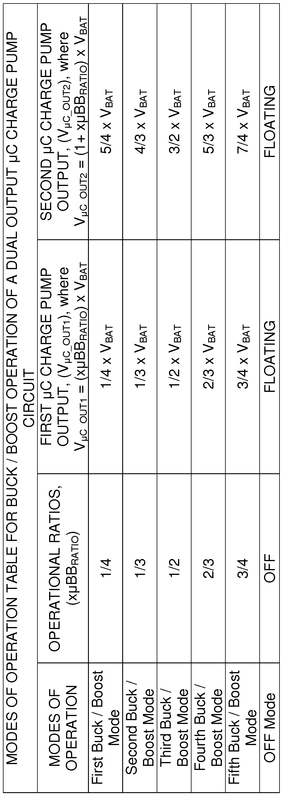
TABLE 2A-1
MODES OF OPERATION TABLE FOR BUCK / BOOST OPERATION OF A DUAL OUTPUT pC CHARGE PUMP
CIRCUIT
FIRST pC CHARGE PUMP SECOND pC CHARGE PUMP
MODES OF OPERATIONAL RATIOS,
OUTPUT, (νμ0_ουτι), where OUTPUT, (νμ0_ουτ2), where OPERATION (χμΒΒΒΑΤιο)
μο ouTi = (1- XMBBRATIO) X VBAT νμο ouT2 = (1 + XMBBRATIO) X VBAT
Sixth Buck / Boost
1/4 3/4 x VBAT 5/4 x VBAT
Mode
Seventh Buck /
1/3 2/3 x VBAT 4/3 x VBAT
Boost Mode
Eigth Buck / Boost
1/2 1/2 x VBAT 3/2 x VBAT
Mode
Ninth Buck / Boost
2/3 1/3 x VBAT 5/3 x VBAT
Mode
Tenth Buck / Boost
3/4 1/4 x VBAT 7/4 x VBAT
Mode
OFF Mode OFF FLOATING FLOATING
TABLE 2A-2
/ o

/ y

ou

TABLE 2B-2A
O I
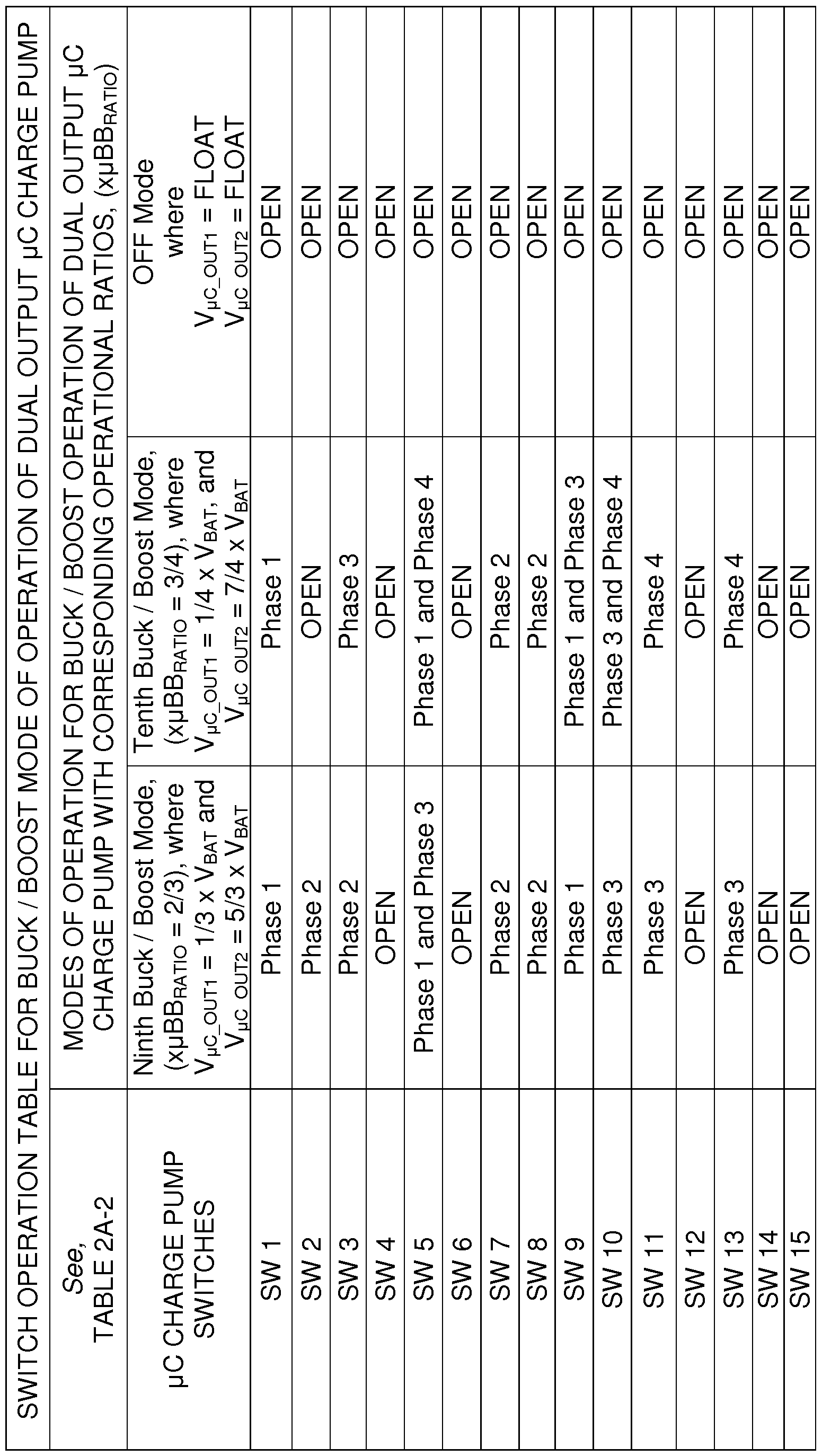
TABLE 2B-2B
[00158] The configurations and operations of the dual output μθ charge pump circuit 1 2A when the dual output μθ charge pump circuit 1 2A operates in the various buck / boost modes, described in the TABLE 2A-1 and the TABLE 2A-2, will now be discussed with reference to the TABLE 2B-1 A, the TABLE 2B-1 B, the TABLE 2B-2A, and the TABLE 2B-2B.
[00159] TABLE 2B-1 A describes, and Figures 8A-B depicts, the operation of the dual output μθ charge pump circuit 12A when the controller 14 configures the dual output iC charge pump circuit 12A to operate in the First Buck / Boost Mode. The controller 14 configures the multiple output μθ charge pump control circuit 72A to use an operational ratio, (XM BBRATIO), set to 1 /4. The multiple output [iC charge pump control circuit 72A operably divides the operation of the dual output [iC charge pump circuit 1 2A into four phases of operation. The multiple output [iC charge pump control circuit 72A operably configures the dual output [iC charge pump switch matrix circuit 70A such that first μθ charge pump output 24 generates a first μθ charge pump output voltage, (VMC_OUTI), substantially equal to 1 /4 x VBAT, and the second μθ charge pump output 26 generates a second μθ charge pump output voltage, (νμ0_ουτ2), substantially equal to 5/4 x VBAT-
[00160] As described in TABLE 2B-1 A and depicted in Figure 8A, in the first phase of operation, (Phase 1 ), the multiple output μθ charge pump control circuit 72A operably closes the first switch 74, (SW 1 ), the fifth switch 82, (SW 5), and the ninth switch 90, (SW 9). In the second phase of operation, (Phase 2), the multiple output μθ charge pump control circuit 72A operably closes the seventh switch 86, (SW 7), and the eighth switch 88, (SW 8). As further depicted in Figure 8B, in the third phase of operation, (Phase 3), the multiple output μθ charge pump control circuit 72A operably closes the third switch 78, (SW 3), the ninth switch 90, (SW 9), and the tenth switch 92, (SW 1 0). In the fourth phase of operation, (Phase 4), the multiple output μθ charge pump control circuit 72A operably closes the tenth switch 92, (SW 1 0), the twelfth switch 96, (SW 12), and the fifteenth switch 1 02, (SW 15).
[00161] As a result, the first flying capacitor 42, (CFLY-I ) , develops a first flying capacitor voltage, (VCAP_ _FLYI)J substantially equal to 1 /2 x VBAT; and the second flying capacitor 44, (CFLY2), develops a second flying capacitor voltage,
(VCAP_FLY2), substantially equal to 1 /4 x VBAT- Accordingly, first μθ charge pump output 24 generates a first μθ charge pump output voltage, (VMC_OUTI ), substantially equal to 1 /4 x VBAT, on the first μθ charge pump output capacitor 46, (Ομο_ουτ-ι), and the second μθ charge pump output 26 generates a secondiC charge pump output voltage, (νμ0_ουτ2), substantially equal to 5/4 x VBAT on the second μθ charge pump output capacitor 48, (Ομο_ουτ2)- [00162] TABLE 2B-1 A describes, and Figure 9 depicts, the operation of the dual output [iC charge pump circuit 12A when the controller 14 configures the dual output [iC charge pump circuit 12A to operate in the Second Buck / Boost Mode. The controller 14 configures the multiple output μθ charge pump control circuit 72A to use an operational ratio,
 set to 1 /3. The multiple output [iC charge pump control circuit 72A operably divides the operation of the dual output [iC charge pump circuit 12A into three phases of operation. The multiple output μθ charge pump control circuit 72A operably configures the dual output [iC charge pump switch matrix circuit 70A such that first μθ charge pump output 24 generates a first μθ charge pump output voltage, (VMC_OUTI ), substantially equal to 1 /3 x VBAT, and the second μθ charge pump output 26 generates a second μθ charge pump output voltage, (νμ0_ουτ2), substantially equal to 4/3 x VBAT-
[00163] As described in TABLE 2B-1 A and depicted in Figure 9, in the first phase of operation, (Phase 1 ), the multiple output μθ charge pump control circuit 72A operably closes the first switch 74, (SW 1 ), the fifth switch 82, (SW 5), and the ninth switch 90, (SW 9). In the second phase of operation, (Phase 2), the multiple output μθ charge pump control circuit 72A operably closes the second switch 76, (SW 2), the third switch 78, (SW 3), the seventh switch 86, (SW 7), and the eighth switch 88, (SW 8). In the third phase of operation, (Phase 3), the multiple output μθ charge pump control circuit 72A operably closes the tenth
switch 92, (SW 10), the eleventh switch 94, (SW 1 1 ), the thirteenth switch 98, (SW 13), and the fifteenth switch 102, (SW 15).
[00164] As a result, the first flying capacitor 42, (CFLYI), develops a first flying capacitor voltage, (VCAP_FLYI), substantially equal to 1 /3 x VBAT, and the second flying capacitor 44, (CFLY2), develops a second flying capacitor voltage,
(VCAP_FLY2), substantially equal to 1 /3 x VBAT- Accordingly, first μθ charge pump output 24 generates a first μθ charge pump output voltage, (VMC_OUTI ),
substantially equal to 1/3 x VBAT, on the first μθ charge pump output capacitor 46, (Ομο_ουτι), and the second μθ charge pump output 26 generates a secondiC charge pump output voltage, (νμ0_ουτ2), substantially equal to 4/3 x VBAT on the second μθ charge pump output capacitor 48, (Ομ0_ουτ2)- [00165] TABLE 2B-1 A describes, and Figure 10 depicts, the operation of the dual output [iC charge pump circuit 12A when the controller 14 configures the dual output [iC charge pump circuit 12A to operate in the Third Buck / Boost Mode. The controller 14 configures the multiple output μθ charge pump control circuit 72A to use an operational ratio, (χμΒΒρ,Α-πο), set to 1 /2. The multiple output [iC charge pump control circuit 72A operably divides the operation of the dual output [iC charge pump circuit 12A into three phases of operation. The multiple output μθ charge pump control circuit 72A operably configures the dual output [iC charge pump switch matrix circuit 70A such that first μθ charge pump output 24 generates a first μθ charge pump output voltage, (νμ0_ουτι),
substantially equal to 1/2 x VBAT, and the second μθ charge pump output 26 generates a second μθ charge pump output voltage, (νμ0_ουτ2), substantially equal to 3/2 x VBAT- [00166] As further described in TABLE 2B-1 A and depicted in Figure 10, in the first phase of operation, (Phase 1 ), the multiple output μθ charge pump control circuit 72A operably closes the first switch 74, (SW 1 ), the fourth switch 80, (SW 4), the fifth switch 82, (SW 5), the sixth switch 84, (SW 6), and the ninth switch 90, (SW 9). In the second phase of operation, (Phase 2), the multiple output μθ charge pump control circuit 72A operably closes the second switch 76, (SW 2), the third switch 78, (SW 3), the seventh switch 86, (SW 7), and the eighth switch
88, (SW 8). In the third phase of operation, (Phase 3), the multiple output μθ charge pump control circuit 72A operably closes the tenth switch 92, (SW 10), the eleventh switch 94, (SW 1 1 ), the thirteenth switch 98, (SW 13), and the fifteenth switch 1 02, (SW 15).
[00167] As a result, the first flying capacitor 42, (CFLY-I ) , develops a first flying capacitor voltage, (VCAP_ _FLYI)J substantially equal to 1 /2 x VBAT; and the second flying capacitor 44, (CFLY2), develops a second flying capacitor voltage,
(VCAP_FLY2), substantially equal to 1 /2 x VBAT- Accordingly, first μθ charge pump output 24 generates a first μθ charge pump output voltage, (VMC_OUTI ), substantially equal to 1 /2 x VBAT, on the first μθ charge pump output capacitor 46, (Ομο_ουτ-ι), and the second μθ charge pump output 26 generates a secondiC charge pump output voltage, (νμ0_ουτ2), substantially equal to 3/2 x VBAT on the second μθ charge pump output capacitor 48, (Ομο_ουτ2)- [00168] TABLE 2B-1 B describes, and Figure 1 1 depicts, the operation of the dual output μθ charge pump circuit 12A when the controller 14 configures the dual output [iC charge pump circuit 12A to operate in the Fourth Buck / Boost Mode. The controller 14 configures the multiple output μθ charge pump control circuit 72A to use an operational ratio,
 set to 2/3. The multiple output [iC charge pump control circuit 72A operably divides the operation of the dual output μθ charge pump circuit 12A into three phases of operation. The multiple output μθ charge pump control circuit 72A operably configures the dual output [iC charge pump switch matrix circuit 70A such that first μθ charge pump output 24 generates a first μθ charge pump output voltage, (VMC_OUTI ), substantially equal to 2/3 x VBAT, and the second μθ charge pump output 26 generates a second μθ charge pump output voltage, (νμ0_ουτ2), substantially equal to 5/3 x VBAT-
[00169] As further described in TABLE 2B-1 B and depicted in Figure 1 1 , in the first phase of operation, (Phase 1 ), the multiple output μθ charge pump control circuit 72A operably closes the first switch 74, (SW 1 ), the fourth switch 80, (SW 4), the sixth switch 84, (SW 6), and the ninth switch 90, (SW 9). In the second phase of operation, (Phase 2), the multiple output μθ charge pump control circuit
72A operably closes the second switch 76, (SW 2), the fifth switch 82, (SW 5), and the eighth switch 88, (SW 8). In the third phase of operation, (Phase 3), the multiple output μθ charge pump control circuit 72A operably closes the fifth switch 82, (SW 5), the tenth switch 92, (SW 10), the eleventh switch 94, (SW 1 1 ), and the thirteenth switch 98, (SW 1 3).
[00170] As a result, the first flying capacitor 42, (CFLY-I ) , develops a first flying capacitor voltage, (VCAP_FLYI), substantially equal to 1 /3 x VBAT, and the second flying capacitor 44, (CFLY2), develops a second flying capacitor voltage,
(VCAP_FLY2), substantially equal to 1 /3 x VBAT- Accordingly, first μθ charge pump output 24 generates a first μθ charge pump output voltage, (VMC_OUTI ),
substantially equal to 2/3 x VBAT, on the first μθ charge pump output capacitor 46, (Ομο_ουτ-ι), and the second μθ charge pump output 26 generates a secondiC charge pump output voltage, (νμ0_ουτ2), substantially equal to 5/3 x VBAT on the second μθ charge pump output capacitor 48, (Ομο_ουτ2)- [00171 ] TABLE 2B-1 B describes, and Figures 1 2A-B depicts, the operation of the dual output μθ charge pump circuit 12A when the controller 14 configures the dual output [iC charge pump circuit 12A to operate in the Fifth Buck / Boost Mode. The controller 14 configures the multiple output μθ charge pump control circuit 72A to use an operational ratio, (χμΒΒρ,Α-πο), set to 3/4. The multiple output [iC charge pump control circuit 72A operably divides the operation of the dual output [iC charge pump circuit 12A into four phases of operation. The multiple output μθ charge pump control circuit 72A operably configures the dual output [iC charge pump switch matrix circuit 70A such that first μθ charge pump output 24 generates a first μθ charge pump output voltage, (VMC_OUTI ),
substantially equal to 3/4 x VBAT, and the second μθ charge pump output 26 generates a second μθ charge pump output voltage, (νμ0_ουτ2), substantially equal to 7/4 x VBAT-
[00172] As further described in TABLE 2B-1 B and depicted in Figure 1 2A, in the first phase of operation, (Phase 1 ), the multiple output μθ charge pump control circuit 72A operably closes the fourth switch 80, (SW 4), the tenth switch 92, (SW 10), and the eleventh switch 94, (SW 1 1 ). In the second phase of
operation, (Phase 2), the multiple output μθ charge pump control circuit 72A operably closes the sixth switch 84, (SW 6), and the ninth switch 90, (SW 9). As further depicted in Figure 1 2B, in the third phase of operation, (Phase 3), the multiple output μθ charge pump control circuit 72A operably closes the second switch 76, (SW 2), the fifth switch 82, (SW 5), and the eighth switch 88, (SW 8). In the fourth phase of operation, (Phase 4), the multiple output μθ charge pump control circuit 72A operably closes the fifth switch 82, (SW 5), the tenth switch 92, (SW 10), the eleventh switch 94, (SW 1 1 ), and the thirteenth switch 98, (SW 1 3).
[00173] As a result, the first flying capacitor 42, (CFLY-I ) , develops a first flying capacitor voltage, (VCAP_FLYI), substantially equal to 1 /2 x VBAT, and the second flying capacitor 44, (CFLY2), develops a second flying capacitor voltage,
(VCAP_FLY2), substantially equal to 1 /4 x VBAT- Accordingly, first μθ charge pump output 24 generates a first μθ charge pump output voltage, (VMC_OUTI ),
substantially equal to 3/4 x VBAT, on the first μθ charge pump output capacitor 46, (Ομο_ουτ-ι), and the second μθ charge pump output 26 generates a secondiC charge pump output voltage, (νμ0_ουτ2), substantially equal to 7/4 x VBAT on the second μθ charge pump output capacitor 48, (Ομο_ουτ2)- [00174] TABLE 2B-2A describes, and Figures 1 3A-B depicts, the operation of the dual output μθ charge pump circuit 12A when the controller 14 configures the dual output [iC charge pump circuit 12A to operate in the Sixth Buck / Boost Mode. The controller 14 configures the multiple output μθ charge pump control circuit 72A to use an operational ratio, (χμΒΒΡιΑ-πο), set to 1 /4. The multiple output [iC charge pump control circuit 72A operably divides the operation of the dual output [iC charge pump circuit 1 2A into four phases of operation. The multiple output [iC charge pump control circuit 72A operably configures the dual output [iC charge pump switch matrix circuit 70A such that first μθ charge pump output 24 generates a first μθ charge pump output voltage, (VMC_OUTI ), substantially equal to 3/4 x VBAT, and the second μθ charge pump output 26 generates a second μθ charge pump output voltage, (νμ0_ουτ2), substantially equal to 5/4 x
VBAT-
[00175] As described in TABLE 2B-2A and depicted in Figure 13A, in the first phase of operation, (Phase 1 ), the multiple output μθ charge pump control circuit 72A operably closes the fourth switch 80, (SW 4), the tenth switch 92, (SW 10), and the eleventh switch 94, (SW 1 1 ). In the second phase of operation, (Phase 2), the multiple output μθ charge pump control circuit 72A operably closes the sixth switch 84, (SW 6), and the ninth switch 90, (SW 9). As further depicted in Figure 13B, in the third phase of operation, (Phase 3), the multiple output μθ charge pump control circuit 72A operably closes the second switch 76, (SW 2), the fifth switch 82, (SW 5), and the eighth switch 88, (SW 8). In the fourth phase of operation, (Phase 4), the multiple output μθ charge pump control circuit 72A operably closes the tenth switch 92, (SW 10), the twelfth switch 96, (SW 12), and the fifteenth switch 102, (SW 15).
[00176] As a result, the first flying capacitor 42, (CFLY-I), develops a first flying capacitor voltage, (VCAP_ _FLYI)J substantially equal to 1 /2 x VBAT; and the second flying capacitor 44, (CFLY2), develops a second flying capacitor voltage,
(VCAP_FLY2), substantially equal to 1 /4 x VBAT- Accordingly, first μθ charge pump output 24 generates a first μθ charge pump output voltage, (VMC_OUTI ), substantially equal to 3/4 x VBAT, on the first μθ charge pump output capacitor 46, (Ομο_ουτ-ι), and the second μθ charge pump output 26 generates a secondiC charge pump output voltage, (νμ0_ουτ2), substantially equal to 5/4 x VBAT on the second μθ charge pump output capacitor 48, (Ομο_ουτ2)- [00177] TABLE 2B-2A describes, and Figure 14 depicts, the operation of the dual output [iC charge pump circuit 12A when the controller 14 configures the dual output [iC charge pump circuit 12A to operate in the Seventh Buck / Boost Mode. The controller 14 configures the multiple output μθ charge pump control circuit 72A to use an operational ratio,
 set to 1 /3. The multiple output [iC charge pump control circuit 72A operably divides the operation of the dual output [iC charge pump circuit 12A into three phases of operation. The multiple output μθ charge pump control circuit 72A operably configures the dual output [iC charge pump switch matrix circuit 70A such that first μθ charge pump output 24 generates a first μθ charge pump output voltage, (VMC_OUTI ),
substantially equal to 2/3 x VBAT, and the second μθ charge pump output 26 generates a second μθ charge pump output voltage, (νμ0_ουτ2), substantially equal to 4/3 x VBAT-
set to 1 /3. The multiple output [iC charge pump control circuit 72A operably divides the operation of the dual output [iC charge pump circuit 12A into three phases of operation. The multiple output μθ charge pump control circuit 72A operably configures the dual output [iC charge pump switch matrix circuit 70A such that first μθ charge pump output 24 generates a first μθ charge pump output voltage, (VMC_OUTI ),
substantially equal to 2/3 x VBAT, and the second μθ charge pump output 26 generates a second μθ charge pump output voltage, (νμ0_ουτ2), substantially equal to 4/3 x VBAT-
[00178] As described in TABLE 2B-2A and depicted in Figure 14, in the first phase of operation, (Phase 1 ), the multiple output μθ charge pump control circuit 72A operably closes the first switch 74, (SW 1 ), the fourth switch 80, (SW 4), the sixth switch 84, (SW 6), and the ninth switch 90, (SW 9). In the second phase of operation, (Phase 2), the multiple output μθ charge pump control circuit 72A operably closes the second switch 76, (SW 2), the fifth switch 82, (SW 5), and the eighth switch 88, (SW 8). In the third phase of operation, (Phase 3), the multiple output μθ charge pump control circuit 72A operably closes the tenth switch 92, (SW 10), the eleventh switch 94, (SW 1 1 ), the thirteenth switch 98, (SW 1 3), and the fifteenth switch 1 02, (SW 1 5).
[00179] As a result, the first flying capacitor 42, (CFLY-I), develops a first flying capacitor voltage, (VCAP_FLYI), substantially equal to 1 /3 x VBAT, and the second flying capacitor 44, (CFLY2), develops a second flying capacitor voltage,
(VCAP_FLY2), substantially equal to 1 /3 x VBAT- Accordingly, first μθ charge pump output 24 generates a first μθ charge pump output voltage, (νμ0_ουτι),
substantially equal to 2/3 x VBAT, on the first μθ charge pump output capacitor 46, (Ομο_ουτ-ι), and the second μθ charge pump output 26 generates a secondiC charge pump output voltage, (νμ0_ουτ2), substantially equal to 4/3 x VBAT on the second μθ charge pump output capacitor 48, (Ομο_ουτ2)- [00180] TABLE 2B-2A describes the operation of the dual output μθ charge pump circuit 12A when the controller 14 configures the dual output μθ charge pump circuit 12A to operate in the Eighth Buck / Boost Mode. The controller 14 configures the multiple output μθ charge pump control circuit 72A to use an operational ratio, (χμΒΒρ,Α-πο), set to 1 /2. The multiple output μθ charge pump control circuit 72A operably divides the operation of the dual output μθ charge pump circuit 12A into three phases of operation. The multiple output μθ charge pump control circuit 72A operably configures the dual output μθ charge pump switch matrix circuit 70A such that first μθ charge pump output 24 generates a
first iC charge pump output voltage, (νμ0_ _ouTi)j substantially equal to 1 /2 x VBAT; and the second μθ charge pump output 26 generates a second μθ charge pump output voltage, (νμ0_ουτ2), substantially equal to 3/2 x VBAT- [00181 ] As further described in TABLE 2B-2A, in the first phase of operation, (Phase 1 ), the multiple output μθ charge pump control circuit 72A operably closes the first switch 74, (SW 1 ), the fourth switch 80, (SW 4), the fifth switch 82, (SW 5), the sixth switch 84, (SW 6), and the ninth switch 90, (SW 9). In the second phase of operation, (Phase 2), the multiple output μθ charge pump control circuit 72A operably closes the second switch 76, (SW 2), the third switch 78, (SW 3), the seventh switch 86, (SW 7), and the eighth switch 88, (SW 8). In the third phase of operation, (Phase 3), the multiple output μθ charge pump control circuit 72A operably closes the tenth switch 92, (SW 1 0), the eleventh switch 94, (SW 1 1 ), the thirteenth switch 98, (SW 1 3), and the fifteenth switch 1 02, (SW 15).
[00182] As a result, the first flying capacitor 42, (CFLYI), develops a first flying capacitor voltage, (VCAP_FLYI), substantially equal to 1 /2 x VBAT, and the second flying capacitor 44, (CFLY2), develops a second flying capacitor voltage,
(VCAP_FLY2), substantially equal to 1 /2 x VBAT- Accordingly, first μθ charge pump output 24 generates a first μθ charge pump output voltage, (VMC_OUTI ),
substantially equal to 1 /2 x VBAT, on the first μθ charge pump output capacitor 46, (Ομο_ουτι), and the second μθ charge pump output 26 generates a second [iC charge pump output voltage, (νμ0_ουτ2), substantially equal to 3/2 x VBAT on the second μθ charge pump output capacitor 48, (Ομ0_ουτ2)- [00183] TABLE 2B-2B describes, and Figure 1 5 depicts, the operation of the dual output μθ charge pump circuit 12A when the controller 14 configures the dual output [iC charge pump circuit 12A to operate in the Ninth Buck / Boost Mode. The controller 14 configures the multiple output μθ charge pump control circuit 72A to use an operational ratio, (χμΒΒρ,Α-πο), set to 2/3. The multiple output [iC charge pump control circuit 72A operably divides the operation of the dual output μθ charge pump circuit 12A into three phases of operation. The multiple output μθ charge pump control circuit 72A operably configures the dual
output μθ charge pump switch matrix circuit 70A such that first μθ charge pump output 24 generates a first μθ charge pump output voltage, (VMC_OUTI ),
substantially equal to 1/3 x VBAT, and the second μθ charge pump output 26 generates a second μθ charge pump output voltage, (νμ0_ουτ2), substantially equal to 5/3 x VBAT-
[00184] As further described in TABLE 2B-2B and depicted in Figure 15, in the first phase of operation, (Phase 1 ), the multiple output μθ charge pump control circuit 72A operably closes the first switch 74, (SW 1 ), the fifth switch 82, (SW 5), and the ninth switch 90, (SW 9). In the second phase of operation, (Phase 2), the multiple output μθ charge pump control circuit 72A operably closes the second switch 76, (SW 2), the third switch 78, (SW 3), the seventh switch 86, (SW 7), and the eighth switch 88, (SW 8). In the third phase of operation, (Phase 3), the multiple output μθ charge pump control circuit 72A operably closes the fifth switch 82, (SW 5), the tenth switch 92, (SW 10), the eleventh switch 94, (SW 1 1 ), and the thirteenth switch 98, (SW 13).
[00185] As a result, the first flying capacitor 42, (CFLYI), develops a first flying capacitor voltage, (VCAP_ _FLYI)J substantially equal to 1 /3 x VBAT; and the second flying capacitor 44, (CFLY2), develops a second flying capacitor voltage,
(VCAP_FLY2), substantially equal to 1 /3 x VBAT- Accordingly, first μθ charge pump output 24 generates a first μθ charge pump output voltage, (VMC_OUTI ),
substantially equal to 1/3 x VBAT, on the first μθ charge pump output capacitor 46, (Ομο_ουτι), and the second μθ charge pump output 26 generates a secondiC charge pump output voltage, (νμ0_ουτ2), substantially equal to 5/3 x VBAT on the second μθ charge pump output capacitor 48, (Ομ0_ουτ2)- [00186] TABLE 2B-2B describes, and Figures 16A-B depicts, the operation of the dual output μθ charge pump circuit 12A when the controller 14 configures the dual output [iC charge pump circuit 12A to operate in the Tenth Buck / Boost Mode. The controller 14 configures the multiple output μθ charge pump control circuit 72A to use an operational ratio, (χμΒΒρ,Ατιο), set to 3/4. The multiple output [iC charge pump control circuit 72A operably divides the operation of the dual output [iC charge pump circuit 12A into four phases of operation. The
multiple output μθ charge pump control circuit 72A operably configures the dual output iC charge pump switch matrix circuit 70A such that first μθ charge pump output 24 generates a first μθ charge pump output voltage, (VMC_OUTI ),
substantially equal to 1/4 x VBAT, and the second μθ charge pump output 26 generates a second μθ charge pump output voltage, (νμ0_ουτ2), substantially equal to 7/4 x VBAT-
[00187] As further described in TABLE 2B-2B and depicted in Figure 16A, in the first phase of operation, (Phase 1 ), the multiple output μθ charge pump control circuit 72A operably closes the first switch 74, (SW 1 ), the fifth switch 82, (SW 5), and the ninth switch 90, (SW 9). In the second phase of operation, (Phase 2), the multiple output μθ charge pump control circuit 72A operably closes the seventh switch 86, (SW 7), and the eighth switch 88, (SW 8). As further depicted in Figure 16B, in the third phase of operation, (Phase 3), the multiple output μθ charge pump control circuit 72A operably closes the third switch 78, (SW 3), the ninth switch 90, (SW 9), and the tenth switch 92, (SW 10). In the fourth phase of operation, (Phase 4), the multiple output μθ charge pump control circuit 72A operably closes the fifth switch 82, (SW 5), the tenth switch 92, (SW 10), the eleventh switch 94, (SW 1 1 ), and the thirteenth switch 98, (SW 13).
[00188] As a result, the first flying capacitor 42, (CFLYI), develops a first flying capacitor voltage, (VCAP_ _FLYI)J substantially equal to 1 /2 x VBAT; and the second flying capacitor 44, (CFLY2), develops a second flying capacitor voltage,
(VCAP_FLY2), substantially equal to 1 /4 x VBAT- Accordingly, first μθ charge pump output 24 generates a first μθ charge pump output voltage, (VMC_OUTI ),
substantially equal to 1/4 x VBAT, on the first μθ charge pump output capacitor 46, (Ομο_ουτι), and the second μθ charge pump output 26 generates a second [iC charge pump output voltage, (νμ0_ουτ2), substantially equal to 7/4 x VBAT on the second μθ charge pump output capacitor 48, (Ομ0_ουτ2)- [00189] Both the TABLE 2B-1 B and the TABLE 2B-2B describe the operation of the dual output μθ charge pump circuit 12A when the controller 14 configures the dual output μθ charge pump circuit 12A to operate in the OFF Mode. As
described in both the TABLE 2B-1 B and the TABLE 2B-2B, when the controller 14 configures the dual output μθ charge pump circuit 1 2A to be in the OFF Mode of operation, the multiple output μθ charge pump control circuit 72A may operablely open the first switch 74, (SW 1 ), the second switch 76, (SW 2), the third switch 78, (SW 3), the fourth switch 80, (SW 4), the fifth switch 82, (SW 5), the sixth switch 84, (SW 6), the seventh switch 86, (SW 7), the eighth switch 88, (SW 8), the ninth switch 90, (SW 9), the tenth switch 92, (SW 1 0), the eleventh switch 94, (SW 1 1 ), the twelfth switch 96, (SW 1 2), the thirteenth switch 98, (SW 1 3), the fourteenth switch 1 00, (SW 14), and the fifteenth switch 1 02, (SW 15). As a result, the first μθ charge pump output voltage, (VMC_OUTI), on the first μθ charge pump output 24 floats relative to ground. Likewise, the second μθ charge pump output voltage, (νμ0_ουτ2), on the second μθ charge pump output 26 floats relative to ground.
[00190] A non-limiting set of example operational modes of the dual output μθ charge pump circuit 1 2A configured to operate in a boost / buck mode of operation will now be discussed. As an example, TABLE 3A-1 and TABLE 3A-2, entitled "MODES OF OPERATION TABLE FOR BOOST / BUCK OPERATION OF A DUAL OUTPUT C CHARGE PUMP CI RCUIT," describe, in tablulated form, several, non-limiting, example modes of operation of the dual output μC charge pump circuit 1 2A configured to operate in a boost / buck mode of operation. As an example, the non-limiting example modes of boost / buck modes of operation described in TABLE 3A-1 include: a First (1 st) Boost / Buck Mode, a Second (2nd) Boost / Buck Mode, a Third (3rd) Boost / Buck Mode, a Fourth (4th) Boost / Buck Mode, a Fifth (5th) Boost / Buck Mode, and an OFF Mode. As another example, the non-limiting example modes of boost / buck modes of operation described in TABLE 3A-2 include: a Sixth (6th) Boost / Buck Mode, a Seventh (7th) Boost / Buck Mode, an Eighth (8th) Boost / Buck Mode, a Ninth (9th) Boost / Buck Mode, a Tenth (1 0th) Boost / Buck Mode, and an OFF Mode.
[00191] As depicted in TABLE 3A-1 and TABLE 3A-2, each example boost / buck mode of operation of the dual output μC charge pump circuit 1 2A
corresponds to an operational ratio, (x BBRATio), where the operational ratio, (X BBRATIO), may provide a relationship between the first μθ charge pump output voltage, (VMC_OUTI), generated by the first μθ charge pump output 24 and the second μθ charge pump output voltage, (νμ0_ουτ2), generated by the second μθ charge pump output 26. The operational ratio, (X BBRATIO), may be an operational ratio parameter that is configured by the controller 14 and stored locally in the multiple output μθ charge pump control circuit 72A.
[00192] For example, TABLE 3A-1 describes example boost / buck modes of operation of the dual output μθ charge pump circuit 12A where the first μθ charge pump output 24 is configured to generate a first μθ charge pump output voltage, (νμ0_ουτι ) such that νμ0_ουτι = (1 + χμΒΒΒΑΤιο) x VBAT- For the sake of convenience, and without limitation, the battery voltage, (VBAT), is used to represent the magnitude of the voltage on the supply voltage 20. The second μθ charge pump output 26 is configured to generate a second μθ charge pump output voltage, (νμ0_ουτ2) such that νμ0_ουτ2 = (χμΒΒΒΑΤιο) x VBAT, where VBAT is used to represent the magnitude of the voltage on the supply voltage 20.
[00193] Accordingly, as described in TABLE 3A-1 , in the First Boost / Buck Mode of operation of the dual output μθ charge pump circuit 12A, the controller 14 configures the multiple output μθ charge pump control circuit 72A to use an operational ratio, (χμΒΒΒΑΤιο), set to 1 /4. As a result, the first μθ charge pump output 24 generates a first μθ charge pump output voltage, (νμ0_ουτι ), substantially equal to 5/4 x VBAT, and the second μθ charge pump output 26 generates a second μθ charge pump output voltage, (νμ0_ουτ2), substantially equal to 1 /4 x VBAT. In the Second Boost / Buck Mode of operation of the dual output iC charge pump circuit 12A, the controller 14 configures the multiple output [iC charge pump control circuit 72A to use an operational ratio,
(χμΒΒρΛτιο), set to 1 /3. As a result, the first μθ charge pump output 24 generates a first μθ charge pump output voltage, (νμ0_ουτι ), substantially equal to 4/3 x VEAT, and the second μθ charge pump output 26 generates a second μθ charge pump output voltage, (νμ0_ουτ2), substantially equal to 1 /3 x VBAT- In the Third Boost / Buck Mode of operation of the dual output μθ charge pump circuit
1 2A, the controller 14 configures the multiple output μθ charge pump control circuit 72A to use an operational ratio, (x BBRATio), set to 1 /2. As a result, the first iC charge pump output 24 generates a first μθ charge pump output voltage, (νμο_ουτι ), substantially equal to 3/2 x VBAT, and the second μθ charge pump output 26 generates a second μθ charge pump output voltage, (νμ0_ουτ2), substantially equal to 1 /2 x VBAT- In the Fourth Boost / Buck Mode of operation of the dual output μθ charge pump circuit 12A, the controller 14 configures the multiple output μθ charge pump control circuit 72A to use an operational ratio, (χμΒΒΒΑτιο), set to 2/3. As a result, the first μθ charge pump output 24
generates a first μθ charge pump output voltage, (νμ0_ _ouTi )j substantially equal to 5/3 x VBAT, and the second μθ charge pump output 26 generates a second μθ charge pump output voltage, (νμ0_ουτ2), substantially equal to 2/3 x VBAT- In the Fifth Boost / Buck Mode of operation of the dual output μθ charge pump circuit 1 2A, the controller 14 configures the multiple output μθ charge pump control circuit 72A to use an operational ratio, (χμΒΒρΑτιο), set to 3/4. As a result, the first [iC charge pump output 24 generates a first μθ charge pump output voltage, (VMC_OUTI ), substantially equal to 7/4 x VBAT, and the second μθ charge pump output 26 generates a second μθ charge pump output voltage, (νμ0_ουτ2), substantially equal to 3/4 x VBAT- In the OFF Mode of operation of the dual output [iC charge pump circuit 1 2A, the controller 14 configures the first μθ charge pump output 24 to float and the second μθ charge pump output 26 to float.
[00194] In contrast, TABLE 3A-2 describes other example boost / buck modes of operation of the dual output μθ charge pump circuit 1 2A where the first μθ charge pump output 24 is configured to generate a first μθ charge pump output voltage, (νμ0_ουτι ) such that νμ0_ουτι = (1 + χμΒΒΒΑτιο) x VBAT- For the sake of convenience, and without limitation, the battery voltage, (VBAT) , is used to represent the magnitude of the voltage on the supply voltage 20. The second μθ charge pump output 26 is configured to generate a second μθ charge pump output voltage, (νμ0_ουτ2) such that νμ0_ουτ2 = (1 - χμΒΒΒΑτιο) x VBAT, where VBAT is used to represent the magnitude of the voltage on the supply voltage 20.
[00195] Accordingly, as described in TABLE 3A-2, in the Sixth Boost / Buck Mode of operation of the dual output μθ charge pump circuit 12A, the controller 14 configures the multiple output μθ charge pump control circuit 72A to use an operational ratio, (χμΒΒρΑτιο), set to 1 /4. As a result, the first μθ charge pump output 24 generates a first μθ charge pump output voltage, (νμ0_ουτι), substantially equal to 5/4 x VBAT, and the second μθ charge pump output 26 generates a second μθ charge pump output voltage, (νμ0_ουτ2), substantially equal to 3/4 x VBAT- In the Seventh Boost / Buck Mode of operation of the dual output iC charge pump circuit 12A, the controller 14 configures the multiple output [iC charge pump control circuit 72A to use an operational ratio,
(χμΒΒρΑτιο), set to 1 /3. As a result, the first μθ charge pump output 24 generates a first μθ charge pump output voltage, (VMC_OUTI), substantially equal to 4/3 x VBAT, and the second μθ charge pump output 26 generates a second μθ charge pump output voltage, (νμ0_ουτ2), substantially equal to 2/3 x VBAT- In the Eighth Boost / Buck Mode of operation of the dual output μθ charge pump circuit 12A, the controller 14 configures the multiple output μθ charge pump control circuit 72A to use an operational ratio, (X BBRATIO), set to 1 /2. As a result, the first [iC charge pump output 24 generates a first μθ charge pump output voltage, (νμο_ουτι), substantially equal to 3/2 x VBAT, and the second μθ charge pump output 26 generates a second μθ charge pump output voltage, (VMC_OUT2), substantially equal to 1/2 x VBAT- In the Ninth Boost / Buck Mode of operation of the dual output μθ charge pump circuit 12A, the controller 14 configures the multiple output μθ charge pump control circuit 72A to use an operational ratio, (χμΒΒρΑτιο), set to 2/3. As a result, the first μθ charge pump output 24 generates a first μθ charge pump output voltage, (νμ0_ _ouTi )j substantially equal to 5/3 x VEAT, and the second μθ charge pump output 26 generates a second μθ charge pump output voltage, (νμ0_ουτ2), substantially equal to 1 /3 x VBAT- In the Tenth Boost / Buck Mode of operation of the dual output μθ charge pump circuit 12A, the controller 14 configures the multiple output μθ charge pump control circuit 72A to use an operational ratio, (X BBRATIO), set to 3/4. As a result, the first [iC charge pump output 24 generates a first μθ charge pump output voltage,
(νμο_ουτι), substantially equal to 7/4 x VBAT, and the second C charge pump output 26 generates a second C charge pump output voltage, (νμ0_ουτ2), substantially equal to 1 /4 x VBAT- In the OFF Mode of operation of the dual outputiC charge pump circuit 1 2A, the controller 14 configures the first C charge pump output 24 to float and the second C charge pump output 26 to float.
[00196] TABLE 3B-1 A and TABLE 3B-1 B, entitled "SWITCH OPERATION TABLE FOR BUCK / BOOST OPERATION OF DUAL OUTPUT pC CHARGE PUMP," describe, in tabular form, the switch state (open or closed) of each of the first switch 74, (SW 1 ), the second switch 76, (SW 2), the third switch 78, (SW 3), the fourth switch 80, (SW 4), the fifth switch 82, (SW 5), the sixth switch 84, (SW 6), the seventh switch 86, (SW 7), the eighth switch 88, (SW 8), the ninth switch 90, (SW 9), the tenth switch 92, (SW 1 0), the eleventh switch 94, (SW 1 1 ), the twelfth switch 96, (SW 1 2), the thirteenth switch 98, (SW 1 3), the fourteenth switch 1 00, (SW 14), and the fifteenth switch 1 02, (SW 15), of the dual output pC charge pump circuit 1 2A when the dual output C charge pump circuit 1 2A is configured to operate in the boost / buck modes of operation described in TABLE 3A-1 . In addition, TABLE 3B-1 A and TABLE 3B-1 B also provide the
corresponding operational ratio, (xpBBRA-no), used by the dual output C charge pump circuit 12A when operating in the boost / buck modes of operation described in TABLE 3A-1 . TABLE 3B-1 A and TABLE 3B-1 B further describe the switch state of each of the first switch 74, (SW 1 ), the second switch 76, (SW 2), the third switch 78, (SW 3), the fourth switch 80, (SW 4), the fifth switch 82, (SW 5), the sixth switch 84, (SW 6), the seventh switch 86, (SW 7), the eighth switch 88, (SW 8), the ninth switch 90, (SW 9), the tenth switch 92, (SW 1 0), the eleventh switch 94, (SW 1 1 ), the twelfth switch 96, (SW 1 2), the thirteenth switch 98, (SW 13), the fourteenth switch 1 00, (SW 14), and the fifteenth switch 1 02, (SW 1 5), relative to the particular phases of operation used by the dual output C charge pump circuit 1 2A when operating in the boost / buck modes of operation described in TABLE 3A-1 .
[00197] TABLE 3B-2A and TABLE 3B-2B, also entitled "SWITCH
OPERATION TABLE FOR BUCK / BOOST OPERATION OF DUAL OUTPUT pC
CHARGE PUMP," describe, in tabular form, the switch state (open or closed) of each of the first switch 74, (SW 1 ), the second switch 76, (SW 2), the third switch 78, (SW 3), the fourth switch 80, (SW 4), the fifth switch 82, (SW 5), the sixth switch 84, (SW 6), the seventh switch 86, (SW 7), the eighth switch 88, (SW 8), the ninth switch 90, (SW 9), the tenth switch 92, (SW 10), the eleventh switch 94, (SW 1 1 ), the twelfth switch 96, (SW 12), the thirteenth switch 98, (SW 13), the fourteenth switch 100, (SW 14), and the fifteenth switch 102, (SW 15), of the dual output iC charge pump circuit 12A when the dual output C charge pump circuit 12A is configured to operate in the boost / buck modes of operation described in TABLE 3A-2. In addition, TABLE 3B-2A and TABLE 3B-2B also provide the corresponding operational ratio, (X BBRATIO), used by the dual output C charge pump circuit 12A when operating in the boost / buck modes of operation described in TABLE 3A-2. TABLE 3B-2A and TABLE 3B-2B further describe the switch state of each of the first switch 74, (SW 1 ), the second switch 76, (SW 2), the third switch 78, (SW 3), the fourth switch 80, (SW 4), the fifth switch 82, (SW 5), the sixth switch 84, (SW 6), the seventh switch 86, (SW 7), the eighth switch 88, (SW 8), the ninth switch 90, (SW 9), the tenth switch 92, (SW 10), the eleventh switch 94, (SW 1 1 ), the twelfth switch 96, (SW 12), the thirteenth switch 98, (SW 13), the fourteenth switch 100, (SW 14), and the fifteenth switch 102, (SW 15), relative to the particular phases of operation used by the dual output C charge pump circuit 12A when operating in the boost / buck modes of operation described in TABLE 3A-2.
[00198] As used in TABLE 3B-1 A, TABLE 3B-1 B, TABLE 3B-2A, and TABLE 3B-2A, "PHASE 1 " indicates that the dual output pC charge pump circuit 12A is configured to operate in a first phase of operation, where the multiple output [iC charge pump control circuit 72A configures the switch state (open or closed) of the identified C charge pump switch to be closed during the time period of the first phase of operation. "PHASE 2" indicates that the dual output [iC charge pump circuit 12A is configured to operate in a second phase of operation, where the multiple output C charge pump control circuit 72A configures the switch state (open or closed) of the identified C charge pump
switch to be closed during the time period of the second phase of operation. "PHASE 3" indicates that the dual output μθ charge pump circuit 12A is configured to operate in a third phase of operation, where the multiple output μθ charge pump control circuit 72A configures the switch state (open or closed) of the identified μθ charge pump switch to be closed during the time period of the third phase of operation. "PHASE 4" indicates that the dual output μθ charge pump circuit 12A is configured to operate in a fourth phase of operation, where the multiple output μθ charge pump control circuit 72A configures the switch state (open or closed) of the identified μθ charge pump switch to be closed during the time period of the fourth phase of operation. "OPEN" indicates that the multiple output μθ charge pump control circuit 72A configures the switch state (open or closed) of the identified switch to be closed during all the phases of operation of the dual output μθ charge pump circuit 12A.
I uu

TABLE 3A-1
I U I

TABLE 3A-2
SWITCH OPERATION TABLE FOR BOOST / BUCK MODE OF OPERATION OF DUAL OUTPUT pC CHARGE PUMP
See, MODES OF OPERATION FOR BOOST / BUCK OPERATION OF DUAL OUTPUT iC
TABLE 3A-1 CHARGE PUMP WITH CORRESPONDING OPERATIONAL RATIOS, (χμΒΒΒΑΤιο)
First Boost / Buck Mode, Second Boost / Buck
Third Boost / Buck Mode,
(X BBRATIO = 1 /4), where Mode,
pC CHARGE PUMP (χμΒΒΒΑΤιο = 1 /2), where
(χμΒΒΒΑΤιο = 1 /3), where
SWITCHES νμ0_ουτι = 5/4 x VBAT
νμ0_ουτι = 4/3 x VBAT, and νμ0_ουτι = 3/2 x VBAT, and and
VuC ouT2 = 1 /4 x VBAT Vyc OUT2 = 1 /3 x VBAT νμο_ουτ2 = 1 /2 x VBAT
SW 1 Phase 1 Phase 1 Phase 1
SW 2 OPEN Phase 3 Phase 3
SW 3 Phase 3 Phase 2 Phase 2
SW 4 OPEN OPEN OPEN
SW 5 Phase 1 Phase 1 OPEN
SW 6 OPEN OPEN Phase 1
SW 7 OPEN Phase 3 Phase 3
SW 8 Phase 2 Phase 2 Phase 2
SW 9 Phase 4 OPEN OPEN
SW 10 Phase 3 and Phase 4 Phase 2 Phase 2
SW 1 1 OPEN Phase 3 Phase 3
SW 12 Phase 1 and Phase 3 Phase 1 Phase 1
SW 13 Phase 2 Phase 2 Phase 2
SW 14 OPEN OPEN Phase 1
SW 15 Phase 4 Phase 3 Phase 3
TA BLE 3B-1 A
I u

I UH-

TABLE 3B-2A
SWITCH OPERATION TABLE FOR BOOST / BUCK MODE OF OPERATION OF DUAL OUTPUT pC CHARGE PUMP
See, MODES OF OPERATION FOR BOOST / BUCK OPERATION OF DUAL OUTPUT iC TABLE 3A-2 CHARGE PUMP WITH CORRESPONDING OPERATIONAL RATIOS, (χμΒΒΒΑΤιο)
Ninth Boost / Buck Mode, Tenth Boost / Buck Mode, OFF Mode
pC CHARGE PUMP (χμΒΒΒΑΤιο = 2/3), where (χμΒΒΒΑΤιο = 3/4), where where
SWITCHES νμ0_ουτι = 5/3 x VBAT and νμ0_ουτι = 7/4 x VBAT, and νμ0 ouTi = FLOAT
yc ouT2 = 1 /3 x VBAT VuC ouT2 = 1 /4 x VBAT VuC ouT2 = FLOAT
SW 1 Phase 1 Phase 1 OPEN
SW 2 Phase 3 Phase 4 OPEN
SW 3 Phase 2 Phase 3 OPEN
SW 4 OPEN OPEN OPEN
SW 5 Phase 1 and Phase 3 Phase 1 and Phase 4 OPEN
SW 6 OPEN OPEN OPEN
SW 7 OPEN OPEN OPEN
SW 8 Phase 2 Phase 2 OPEN
SW 9 OPEN OPEN OPEN
SW 10 Phase 2 Phase 3 OPEN
SW 1 1 Phase 3 Phase 4 OPEN
SW 12 Phase 1 Phase 1 and Phase 3 OPEN
SW 13 Phase 2 Phase 2 OPEN
SW 14 OPEN OPEN OPEN
SW 15 OPEN OPEN OPEN
TABLE 3B-2B
[00199] The configurations and operations of the dual output μθ charge pump circuit 1 2A when the dual output μθ charge pump circuit 1 2A operates in the various boost / buck modes, described in the TABLE 3A-1 and the TABLE 3A-2, will now be discussed with reference to the TABLE 3B-1 A, the TABLE 3B-1 B, the TABLE 3B-2A, and the TABLE 3B-2B.
[00200] TABLE 3B-1 A describes, and Figures 1 7A-B depicts, the operation of the dual output μθ charge pump circuit 12A when the controller 14 configures the dual output iC charge pump circuit 12A to operate in the First Boost / Buck Mode. The controller 14 configures the multiple output μθ charge pump control circuit 72A to use an operational ratio, (XM BBRATIO), set to 1 /4. The multiple output [iC charge pump control circuit 72A operably divides the operation of the dual output [iC charge pump circuit 1 2A into four phases of operation. The multiple output [iC charge pump control circuit 72A operably configures the dual output [iC charge pump switch matrix circuit 70A such that first μθ charge pump output 24 generates a first μθ charge pump output voltage, (VMC_OUTI), substantially equal to 5/4 x VBAT, and the second μθ charge pump output 26 generates a second μθ charge pump output voltage, (νμ0_ουτ2), substantially equal to 1 /4 x VBAT-
[00201] As described in TABLE 3B-1 A and depicted in Figure 1 7A, in the first phase of operation, (Phase 1 ), the multiple output μθ charge pump control circuit 72A operably closes the first switch 74, (SW 1 ), the fifth switch 82, (SW 5), and the twelfth switch 96, (SW 1 2). In the second phase of operation, (Phase 2), the multiple output μθ charge pump control circuit 72A operably closes the eighth switch 88, (SW 8) and the thirteenth switch 98, (SW 1 3). As further depicted in Figure 1 7B, in the third phase of operation, (Phase 3), the multiple output μθ charge pump control circuit 72A operably closes the third switch 78, (SW 3), the tenth switch 92, (SW 10), and the twelfth switch 96, (SW 1 2). In the fourth phase of operation, (Phase 4), the multiple output μθ charge pump control circuit 72A operably closes the ninth switch 90, (SW 9), the tenth switch 92, (SW 1 0), and the fifteenth switch 1 02, (SW 15).
[00202] As a result, the first flying capacitor 42, (CFLY-I ) , develops a first flying capacitor voltage, (VCAP_ _FLYI)J substantially equal to 1 /2 x VBAT; and the second flying capacitor 44, (CFLY2), develops a second flying capacitor voltage,
(VCAP_FLY2), substantially equal to 1 /4 x VBAT- Accordingly, first μθ charge pump output 24 generates a first μθ charge pump output voltage, (VMC_OUTI ), substantially equal to 5/4 x VBAT, on the first μθ charge pump output capacitor 46, (Ομο_ουτ-ι), and the second μθ charge pump output 26 generates a secondiC charge pump output voltage, (νμ0_ουτ2), substantially equal to 1 /4 x VBAT on the second μθ charge pump output capacitor 48, (Ομο_ουτ2)- [00203] TABLE 3B-1 A describes, and Figure 1 8 depicts, the operation of the dual output [iC charge pump circuit 12A when the controller 14 configures the dual output [iC charge pump circuit 12A to operate in the Second Boost / Buck Mode. The controller 14 configures the multiple output μθ charge pump control circuit 72A to use an operational ratio,
 set to 1 /3. The multiple output [iC charge pump control circuit 72A operably divides the operation of the dual output [iC charge pump circuit 12A into three phases of operation. The multiple output μθ charge pump control circuit 72A operably configures the dual output [iC charge pump switch matrix circuit 70A such that first μθ charge pump output 24 generates a first μθ charge pump output voltage, (VMC_OUTI ), substantially equal to 4/3 x VBAT, and the second μθ charge pump output 26 generates a second μθ charge pump output voltage, (νμ0_ουτ2), substantially equal to 1 /3 x VBAT-
[00204] As described in TABLE 3B-1 A and depicted in Figure 1 8, in the first phase of operation, (Phase 1 ), the multiple output μθ charge pump control circuit 72A operably closes the first switch 74, (SW 1 ), the fifth switch 82, (SW 5), and the tenth switch 92, (SW 1 0). In the second phase of operation, (Phase 2), the multiple output μθ charge pump control circuit 72A operably closes the third switch 78, (SW 3), the eighth switch 88, (SW 8), the tenth switch 92, (SW 10), and the thirteenth switch 98, (SW 1 3). In the third phase of operation, (Phase 3), the multiple output μθ charge pump control circuit 72A operably closes the
second switch 76, (SW 2), the seventh switch 86, (SW 7), the eleventh switch 94, (SW 1 1 ), and the fifteenth switch 102, (SW 15).
[00205] As a result, the first flying capacitor 42, (CFLYI), develops a first flying capacitor voltage, (VCAP_FLYI), substantially equal to 1 /3 x VBAT, and the second flying capacitor 44, (CFLY2), develops a second flying capacitor voltage,
(VCAP_FLY2), substantially equal to 1 /3 x VBAT- Accordingly, first μθ charge pump output 24 generates a first μθ charge pump output voltage, (VMC_OUTI ),
substantially equal to 4/3 x VBAT, on the first μθ charge pump output capacitor 46, (Ομο_ουτι), and the second μθ charge pump output 26 generates a secondiC charge pump output voltage, (νμ0_ουτ2), substantially equal to 1 /3 x VBAT on the second μθ charge pump output capacitor 48, (Ομ0_ουτ2)- [00206] TABLE 3B-1 A describes, and Figure 19 depicts, the operation of the dual output [iC charge pump circuit 12A when the controller 14 configures the dual output [iC charge pump circuit 12A to operate in the Third Boost / Buck Mode. The controller 14 configures the multiple output μθ charge pump control circuit 72A to use an operational ratio, (χμΒΒρ,Α-πο), set to 1 /2. The multiple output [iC charge pump control circuit 72A operably divides the operation of the dual output [iC charge pump circuit 12A into three phases of operation. The multiple output μθ charge pump control circuit 72A operably configures the dual output [iC charge pump switch matrix circuit 70A such that first μθ charge pump output 24 generates a first μθ charge pump output voltage, (νμ0_ουτι),
substantially equal to 3/2 x VBAT, and the second μθ charge pump output 26 generates a second μθ charge pump output voltage, (νμ0_ουτ2), substantially equal to 1 /2 x VBAT- [00207] As further described in TABLE 3B-1 A and depicted in Figure 19, in the first phase of operation, (Phase 1 ), the multiple output μθ charge pump control circuit 72A operably closes the first switch 74, (SW 1 ), the sixth switch 84, (SW 6), the twelfth switch 96, (SW 12), and the fourteenth switch 100, (SW 14). In the second phase of operation, (Phase 2), the multiple output μθ charge pump control circuit 72A operably closes the third switch 78, (SW 3), the eighth switch 88, (SW 8), the tenth switch 92, (SW 10), and the thirteenth switch 98, (SW 13).
In the third phase of operation, (Phase 3), the multiple output μθ charge pump control circuit 72A operably closes the second switch 76, (SW 2), the seventh switch 86, (SW 7), the eleventh switch 94, (SW 1 1 ), and the fifteenth switch 1 02, (SW 1 5).
[00208] As a result, the first flying capacitor 42, (CFLY-I ) , develops a first flying capacitor voltage, (VCAP_ _FLYI)J substantially equal to 1 /2 x VBAT; and the second flying capacitor 44, (CFLY2), develops a second flying capacitor voltage,
(VCAP_FLY2), substantially equal to 1 /2 x VBAT- Accordingly, first μθ charge pump output 24 generates a first μθ charge pump output voltage, (VMC_OUTI ), substantially equal to 3/2 x VBAT, on the first μθ charge pump output capacitor 46, (Ομο_ουτ-ι), and the second μθ charge pump output 26 generates a secondiC charge pump output voltage, (νμ0_ουτ2), substantially equal to 1 /2 x VBAT on the second μθ charge pump output capacitor 48, (Ομο_ουτ2)- [00209] TABLE 3B-1 B describes, and Figure 20 depicts, the operation of the dual output μθ charge pump circuit 12A when the controller 14 configures the dual output [iC charge pump circuit 12A to operate in the Fourth Boost / Buck Mode. The controller 14 configures the multiple output μθ charge pump control circuit 72A to use an operational ratio,
 set to 2/3. The multiple output [iC charge pump control circuit 72A operably divides the operation of the dual output μθ charge pump circuit 12A into three phases of operation. The multiple output μθ charge pump control circuit 72A operably configures the dual output [iC charge pump switch matrix circuit 70A such that first μθ charge pump output 24 generates a first μθ charge pump output voltage, (VMC_OUTI ), substantially equal to 5/3 x VBAT, and the second μθ charge pump output 26 generates a second μθ charge pump output voltage, (νμ0_ουτ2), substantially equal to 2/3 x VBAT-
[00210] As further described in TABLE 3B-1 B and depicted in Figure 20, in the first phase of operation, (Phase 1 ), the multiple output μθ charge pump control circuit 72A operably closes the first switch 74, (SW 1 ), the sixth switch 84, (SW 6), the twelfth switch 96, (SW 1 2), and the fourteenth switch 1 00, (SW 14). In the second phase of operation, (Phase 2), the multiple output μθ charge pump
control circuit 72A operably closes the fifth switch 82, (SW 5), the eighth switch 88, (SW 8), the tenth switch 92, (SW 1 0), and the thirteenth switch 98, (SW 1 3). In the third phase of operation, (Phase 3), the multiple output μθ charge pump control circuit 72A operably closes the second switch 76, (SW 2), the fifth switch 82, (SW 5), and the eleventh switch 94, (SW 1 1 ).
[00211 ] As a result, the first flying capacitor 42, (CFLY-I ) , develops a first flying capacitor voltage, (VCAP_FLYI), substantially equal to 1 /3 x VBAT, and the second flying capacitor 44, (CFLY2), develops a second flying capacitor voltage,
(VCAP_FLY2), substantially equal to 1 /3 x VBAT- Accordingly, first μθ charge pump output 24 generates a first μθ charge pump output voltage, (VMC_OUTI ), substantially equal to 5/3 x VBAT, on the first μθ charge pump output capacitor 46, (Ομο_ουτ-ι), and the second μθ charge pump output 26 generates a secondiC charge pump output voltage, (νμ0_ουτ2), substantially equal to 2/3 x VBAT on the second μθ charge pump output capacitor 48, (Ομο_ουτ2)- [00212] TABLE 3B-1 B describes, and Figures 21 A-B depicts, the operation of the dual output μθ charge pump circuit 12A when the controller 14 configures the dual output [iC charge pump circuit 12A to operate in the Fifth Boost / Buck Mode. The controller 14 configures the multiple output μθ charge pump control circuit 72A to use an operational ratio, (χμΒΒρ,Α-πο), set to 3/4. The multiple output [iC charge pump control circuit 72A operably divides the operation of the dual output [iC charge pump circuit 12A into four phases of operation. The multiple output μθ charge pump control circuit 72A operably configures the dual output [iC charge pump switch matrix circuit 70A such that first μθ charge pump output 24 generates a first μθ charge pump output voltage, (VMC_OUTI ), substantially equal to 7/4 x VBAT, and the second μθ charge pump output 26 generates a second μθ charge pump output voltage, (νμ0_ουτ2), substantially equal to 3/4 x VBAT-
[00213] As further described in TABLE 3B-1 B and depicted in Figure 21 A, in the first phase of operation, (Phase 1 ), the multiple output μθ charge pump control circuit 72A operably closes the tenth switch 92, (SW 1 0), the eleventh switch 94, (SW 1 1 ), and the fourteenth switch 1 00, (SW 14). In the second
phase of operation, (Phase 2), the multiple output μθ charge pump control circuit 72A operably closes the sixth switch 84, (SW 6), and the twelfth switch 96, (SW 1 2). As further depicted in Figure 21 B, in the third phase of operation, (Phase 3), the multiple output μθ charge pump control circuit 72A operably closes the fifth switch 82, (SW 5), the eighth switch 88, (SW 8), the tenth switch 92, (SW 10), and the thirteenth switch 98, (SW 1 3). In the fourth phase of operation, (Phase 4), the multiple output μθ charge pump control circuit 72A operably closes the second switch 76, (SW 2), the fifth switch 82, (SW 5), and the eleventh switch 94, (SW 1 1 ).
[00214] As a result, the first flying capacitor 42, (CFLY-I ) , develops a first flying capacitor voltage, (VCAP_FLYI), substantially equal to 1 /2 x VBAT, and the second flying capacitor 44, (CFLY2), develops a second flying capacitor voltage,
(VCAP_FLY2), substantially equal to 1 /4 x VBAT- Accordingly, first μθ charge pump output 24 generates a first μθ charge pump output voltage, (VMC_OUTI ),
substantially equal to 7/4 x VBAT, on the first μθ charge pump output capacitor 46, (Ομο_ουτ-ι), and the second μθ charge pump output 26 generates a secondiC charge pump output voltage, (νμ0_ουτ2), substantially equal to 3/4 x VBAT on the second μθ charge pump output capacitor 48, (Ομο_ουτ2)- [00215] TABLE 3B-2A describes, and Figures 22A-B depicts, the operation of the dual output μθ charge pump circuit 12A when the controller 14 configures the dual output [iC charge pump circuit 12A to operate in the Sixth Boost / Buck Mode. The controller 14 configures the multiple output μθ charge pump control circuit 72A to use an operational ratio, (χμΒΒΡιΑ-πο), set to 1 /4. The multiple output [iC charge pump control circuit 72A operably divides the operation of the dual output [iC charge pump circuit 1 2A into four phases of operation. The multiple output [iC charge pump control circuit 72A operably configures the dual output [iC charge pump switch matrix circuit 70A such that first μθ charge pump output 24 generates a first μθ charge pump output voltage, (VMC_OUTI ), substantially equal to 5/4 x VBAT, and the second μθ charge pump output 26 generates a second μθ charge pump output voltage, (νμ0_ουτ2), substantially equal to 3/4 x
VBAT-
[00216] As described in TABLE 3B-2A and depicted in Figure 22A, in the first phase of operation, (Phase 1 ), the multiple output μθ charge pump control circuit 72A operably closes the tenth switch 92, (SW 1 0), the eleventh switch 94, (SW 1 1 ), and the fourteenth switch 1 00, (SW 14). In the second phase of operation, (Phase 2), the multiple output μθ charge pump control circuit 72A operably closes the sixth switch 84, (SW 6), and the twelfth switch 96, (SW 1 2). As further depicted in Figure 22B, in the third phase of operation, (Phase 3), the multiple output iC charge pump control circuit 72A operably closes the fifth switch 82, (SW 5), the eighth switch 88, (SW 8), the tenth switch 92, (SW 10), and the thirteenth switch 98, (SW 1 3).. In the fourth phase of operation, (Phase 4), the multiple output μθ charge pump control circuit 72A operably closes the ninth switch 90, (SW 9), the tenth switch 92, (SW 10), and the fifteenth switch 1 02, (SW 1 5).
[00217] As a result, the first flying capacitor 42, (CFLY-I ) , develops a first flying capacitor voltage, (VCAP_FLYI), substantially equal to 1 /2 x VBAT, and the second flying capacitor 44, (CFLY2), develops a second flying capacitor voltage,
(VCAP_FLY2), substantially equal to 1 /4 x VBAT- Accordingly, first μθ charge pump output 24 generates a first μθ charge pump output voltage, (VMC_OUTI ), substantially equal to 5/4 x VBAT, on the first μθ charge pump output capacitor 46, (Ομο_ουτ-ι), and the second μθ charge pump output 26 generates a second [iC charge pump output voltage, (νμ0_ουτ2), substantially equal to 3/4 x VBAT on the second μθ charge pump output capacitor 48, (Ομο_ουτ2)- [00218] TABLE 3B-2A describes, and Figure 23 depicts, the operation of the dual output [iC charge pump circuit 12A when the controller 14 configures the dual output μθ charge pump circuit 12A to operate in the Seventh Boost / Buck Mode. The controller 14 configures the multiple output μθ charge pump control circuit 72A to use an operational ratio, (χμΒΒρ,Α-πο), set to 1 /3. The multiple output [iC charge pump control circuit 72A operably divides the operation of the dual output [iC charge pump circuit 12A into three phases of operation. The multiple output μθ charge pump control circuit 72A operably configures the dual output [iC charge pump switch matrix circuit 70A such that first μθ charge pump
output 24 generates a first μθ charge pump output voltage, (VMC_OUTI ),
substantially equal to 4/3 x VBAT, and the second μθ charge pump output 26 generates a second μθ charge pump output voltage, (νμ0_ουτ2), substantially equal to 2/3 x VBAT- [00219] As described in TABLE 3B-2A and depicted in Figure 23, in the first phase of operation, (Phase 1 ), the multiple output μθ charge pump control circuit 72A operably closes the first switch 74, (SW 1 ), the sixth switch 84, (SW 6), the twelfth switch 96, (SW 1 2), and the fourteenth switch 1 00, (SW 14). In the second phase of operation, (Phase 2), the multiple output μθ charge pump control circuit 72A operably closes the fifth switch 82, (SW 5), the eighth switch 88, (SW 8), the tenth switch 92, (SW 1 0), and the thirteenth switch 98, (SW 1 3). In the third phase of operation, (Phase 3), the multiple output μθ charge pump control circuit 72A operably closes the second switch 76, (SW 2), the seventh switch 86, (SW 7), the eleventh switch 94, (SW 1 1 ), and the fifteenth switch 1 02, (SW 1 5).
[00220] As a result, the first flying capacitor 42, (CFLYI), develops a first flying capacitor voltage, (VCAP_ _FLYI)J substantially equal to 1 /3 x VBAT; and the second flying capacitor 44, (CFLY2), develops a second flying capacitor voltage,
(VCAP_FLY2), substantially equal to 1 /3 x VBAT- Accordingly, first μθ charge pump output 24 generates a first μθ charge pump output voltage, (VMC_OUTI ),
substantially equal to 4/3 x VBAT, on the first μθ charge pump output capacitor 46, (Ομο_ουτι), and the second μθ charge pump output 26 generates a secondiC charge pump output voltage, (νμ0_ουτ2), substantially equal to 2/3 x VBAT on the second μθ charge pump output capacitor 48, (Ομ0_ουτ2)- [00221 ] TABLE 3B-2A describes the operation of the dual output μθ charge pump circuit 12A when the controller 14 configures the dual output μθ charge pump circuit 12A to operate in the Eighth Boost / Buck Mode. The controller 14 configures the multiple output μθ charge pump control circuit 72A to use an operational ratio, (χμΒΒρ,Ατιο), set to 1 /2. The multiple output μθ charge pump control circuit 72A operably divides the operation of the dual output μθ charge pump circuit 12A into three phases of operation. The multiple output μθ charge
pump control circuit 72A operably configures the dual output μθ charge pump switch matrix circuit 70A such that first μθ charge pump output 24 generates a first iC charge pump output voltage, (VMC_OUTI ), substantially equal to 3/2 x VBAT, and the second μθ charge pump output 26 generates a second μθ charge pump output voltage, (νμ0_ουτ2), substantially equal to 1 /2 x VBAT-
[00222] As further described in TABLE 3B-2A, in the first phase of operation, (Phase 1 ), the multiple output μθ charge pump control circuit 72A operably closes the first switch 74, (SW 1 ), the sixth switch 84, (SW 6), the twelfth switch 96, (SW 12), and the fourteenth switch 100, (SW 14). In the second phase of operation, (Phase 2), the multiple output μθ charge pump control circuit 72A operably closes the third switch 78, (SW 3), the eighth switch 88, (SW 8), the tenth switch 92, (SW 10), and the thirteenth switch 98, (SW 13). In the third phase of operation, (Phase 3), the multiple output μθ charge pump control circuit 72A operably closes the second switch 76, (SW 2), the seventh switch 86, (SW 7), the eleventh switch 94, (SW 1 1 ), and the fifteenth switch 102, (SW 15).
[00223] As a result, the first flying capacitor 42, (CFLYI), develops a first flying capacitor voltage, (VCAP_ _FLYI)J substantially equal to 1 /2 x VBAT; and the second flying capacitor 44, (CFLY2), develops a second flying capacitor voltage,
(VCAP_FLY2), substantially equal to 1 /2 x VBAT- Accordingly, first μθ charge pump output 24 generates a first μθ charge pump output voltage, (VMC_OUTI ),
substantially equal to 3/2 x VBAT, on the first μθ charge pump output capacitor 46, (Ομο_ουτι), and the second μθ charge pump output 26 generates a second [iC charge pump output voltage, (νμ0_ουτ2), substantially equal to 1 /2 x VBAT on the second μθ charge pump output capacitor 48, (Ομ0_ουτ2)- [00224] TABLE 3B-2B describes, and Figure 24 depicts, the operation of the dual output [iC charge pump circuit 12A when the controller 14 configures the dual output [iC charge pump circuit 12A to operate in the Ninth Boost / Buck Mode. The controller 14 configures the multiple output μθ charge pump control circuit 72A to use an operational ratio, (χμΒΒρ,Ατιο), set to 2/3. The multiple output [iC charge pump control circuit 72A operably divides the operation of the dual output [iC charge pump circuit 12A into three phases of operation. The
multiple output μθ charge pump control circuit 72A operably configures the dual output iC charge pump switch matrix circuit 70A such that first μθ charge pump output 24 generates a first μθ charge pump output voltage, (VMC_OUTI ),
substantially equal to 5/3 x VBAT, and the second μθ charge pump output 26 generates a second μθ charge pump output voltage, (νμ0_ουτ2), substantially equal to 1 /3 x VBAT-
[00225] As further described in TABLE 3B-2B and depicted in Figure 24, in the first phase of operation, (Phase 1 ), the multiple output μθ charge pump control circuit 72A operably closes the first switch 74, (SW 1 ), the fifth switch 82, (SW 5), and the twelfth switch 96, (SW 12). In the second phase of operation, (Phase 2), the multiple output μθ charge pump control circuit 72A operably closes the third switch 78, (SW 3), the eighth switch 88, (SW 8), the tenth switch 92, (SW 10), and the thirteenth switch 98, (SW 13). In the third phase of operation, (Phase 3), the multiple output μθ charge pump control circuit 72A operably closes the second switch 76, (SW 2), the fifth switch 82, (SW 5), and the eleventh switch 94, (SW 1 1 ).
[00226] As a result, the first flying capacitor 42, (CFLY-I), develops a first flying capacitor voltage, (VCAP_ _FLYI)J substantially equal to 1 /3 x VBAT; and the second flying capacitor 44, (CFLY2), develops a second flying capacitor voltage,
(VCAP_FLY2), substantially equal to 1 /3 x VBAT- Accordingly, first μθ charge pump output 24 generates a first μθ charge pump output voltage, (νμ0_ουτι),
substantially equal to 5/3 x VBAT, on the first μθ charge pump output capacitor 46, (Ομο_ουτ-ι), and the second μθ charge pump output 26 generates a second [iC charge pump output voltage, (νμ0_ουτ2), substantially equal to 1 /3 x VBAT on the second μθ charge pump output capacitor 48, (Ομο_ουτ2)-
[00227] TABLE 3B-2B describes, and Figures 25A-B depicts, the operation of the dual output μθ charge pump circuit 12A when the controller 14 configures the dual output [iC charge pump circuit 12A to operate in the Tenth Boost / Buck Mode. The controller 14 configures the multiple output μθ charge pump control circuit 72A to use an operational ratio,
 set to 3/4. The multiple output [iC charge pump control circuit 72A operably divides the operation of the
dual output μθ charge pump circuit 12A into four phases of operation. The multiple output μθ charge pump control circuit 72A operably configures the dual output iC charge pump switch matrix circuit 70A such that first μθ charge pump output 24 generates a first μθ charge pump output voltage, (VMC_OUTI ),
set to 3/4. The multiple output [iC charge pump control circuit 72A operably divides the operation of the
dual output μθ charge pump circuit 12A into four phases of operation. The multiple output μθ charge pump control circuit 72A operably configures the dual output iC charge pump switch matrix circuit 70A such that first μθ charge pump output 24 generates a first μθ charge pump output voltage, (VMC_OUTI ),
substantially equal to 7/4 x VBAT, and the second μθ charge pump output 26 generates a second μθ charge pump output voltage, (νμ0_ουτ2), substantially equal to 1 /4 x VBAT-
[00228] As further described in TABLE 3B-2B and depicted in Figure 25A, in the first phase of operation, (Phase 1 ), the multiple output μθ charge pump control circuit 72A operably closes the first switch 74, (SW 1 ), the fifth switch 82, (SW 5), and the twelfth switch 96, (SW 12). In the second phase of operation, (Phase 2), the multiple output μθ charge pump control circuit 72A operably closes the eighth switch 88, (SW 8), and the thirteenth switch 98, (SW 13). As further depicted in Figure 25B, in the third phase of operation, (Phase 3), the multiple output μθ charge pump control circuit 72A operably closes the third switch 78, (SW 3), the tenth switch 92, (SW 10), and the twelfth switch 96, (SW 12). In the fourth phase of operation, (Phase 4), the multiple output μθ charge pump control circuit 72A operably closes the second switch 76, (SW 2), the fifth switch 82, (SW 5), and the eleventh switch 94, (SW 1 1 ).
[00229] As a result, the first flying capacitor 42, (CFLYI), develops a first flying capacitor voltage, (VCAP_ _FLYI)J substantially equal to 1 /2 x VBAT; and the second flying capacitor 44, (CFLY2), develops a second flying capacitor voltage,
(VCAP_FLY2), substantially equal to 1 /4 x VBAT- Accordingly, first μθ charge pump output 24 generates a first μθ charge pump output voltage, (VMC_OUTI ),
substantially equal to 7/4 x VBAT, on the first μθ charge pump output capacitor 46, (Ομο_ουτι), and the second μθ charge pump output 26 generates a second [iC charge pump output voltage, (νμ0_ουτ2), substantially equal to 1 /4 x VBAT on the second μθ charge pump output capacitor 48, (Ομ0_ουτ2)- [00230] Both the TABLE 3B-1 B and the TABLE 3B-2B describe the operation of the dual output μθ charge pump circuit 12A when the controller 14 configures the dual output μθ charge pump circuit 12A to operate in the OFF Mode. As
described in both the TABLE 3B-1 B and the TABLE 3B-2B, when the controller 14 configures the dual output μθ charge pump circuit 12A to be in the OFF Mode of operation, the multiple output μθ charge pump control circuit 72A may operablely open the first switch 74, (SW 1 ), the second switch 76, (SW 2), the third switch 78, (SW 3), the fourth switch 80, (SW 4), the fifth switch 82, (SW 5), the sixth switch 84, (SW 6), the seventh switch 86, (SW 7), the eighth switch 88, (SW 8), the ninth switch 90, (SW 9), the tenth switch 92, (SW 10), the eleventh switch 94, (SW 1 1 ), the twelfth switch 96, (SW 12), the thirteenth switch 98, (SW 13), the fourteenth switch 100, (SW 14), and the fifteenth switch 102, (SW 15). As a result, the first μθ charge pump output voltage, (VMC_OUTI), on the first μθ charge pump output 24 floats relative to ground. Likewise, the second μθ charge pump output voltage, (νμ0_ουτ2), on the second μθ charge pump output 26 floats relative to ground.
[00231] Figure 2B depicts another embodiment of the dual output μθ charge pump circuit 12, depicted in Figure 1 A, as a dual output μθ charge pump circuit 12B. The dual output μθ charge pump circuit 12B is similar in form and function to the dual output μθ charge pump circuit 12A depicted in Figure 2A except as described as follows: (1 ) the dual output μθ charge pump circuit 12B includes a multiple output μθ charge pump switch matrix and control circuit 40B instead of the multiple output μθ charge pump switch matrix and control circuit 40A; (2) the dual output iC charge pump circuit 12B includes the dual output μθ charge pump switch matrix circuit 70B instead of the dual output μθ charge pump switch matrix circuit 70A; and (3) the dual output μθ charge pump circuit 12B includes a multiple output μθ charge pump control circuit 72B instead of a the multiple output [iC charge pump control circuit 72A.
[00232] Unlike the dual output μθ charge pump switch matrix circuit 70A of the multiple output μθ charge pump switch matrix and control circuit 40A, the dual output [iC charge pump switch matrix circuit 70B omits the twelfth switch 96, (SW 12), and the fourteenth switch 100, (SW 14), as depicted in Figure 2A.
Accordingly, the multiple output μθ charge pump control circuit 72B of the dual output [iC charge pump circuit 12B, depicted in Figure 2B, omits both a twelfth
switch control configured to provide a twelfth switch control signal 130 to control the twelfth switch 96, (SW 12) and a fourteenth switch control configured to provide a twelfth switch control signal 130 to control the fourteenth switch 100, (SW 14), as depicted in Figure 2A.
[00233] Even so, because the dual output μθ charge pump circuit 12B is otherwise similar in form and function to the dual output μθ charge pump circuit 12A depicted in Figure 2A, the controller 14 may configure the dual output μθ charge pump circuit 12B to operate in any of the modes of operation that may be performed by the dual output μθ charge pump circuit 12A, as described above, that do not require either the twelfth switch 96, (SW 12), the fourteenth switch 100, (SW 14), or a combination thereof, to be closed. Accordingly, for the sake of brevity, the specific operational modes of the dual output μθ charge pump circuit 12B will not be discussed in detail. Although the specific operational modes of the dual output μθ charge pump circuit 12B are not specifically discussed in detail, the modes of operation of the dual output μθ charge pump circuit 12B, as would be evident to one of ordinary skill in the art, are thereby considered to be within the scope of the concepts disclosed with respect to the modes of operation of the dual output μθ charge pump circuit 12B.
[00234] Accordingly, the dual output μθ charge pump circuit 12B provides an advantage of being able to perform many of the numerous modes of operation of the dual output μθ charge pump circuit 12A without the added complexity of including the twelfth switch 96, (SW 12), the fourteenth switch 100, (SW 14), or a combination thereof. As a result, in come embodiments, the dual output μθ charge pump circuit 12B may be used to reduce both silicon foot print and power requirement of the multiple output μθ charge pump system 10A. This advantage is particularly useful in cases where the supply voltage 20 may be derived from a battery 22, as depicted in Figure 1 A. In addition, as discussed above relative to the embodiments of the dual output μθ charge pump circuit 12, depicted in Figure 1 A, and the dual output μθ charge pump circuit 12A, depicted in Figure 2A, some embodiments of dual output μθ charge pump circuit 12B may include and use more than two flying capactiors to generate the first μθ charge pump
output voltage, (VMC_OUTI ), on the first μθ charge pump output 24 and the secondiC charge pump output voltage, (νμ0_ουτ2), on the second μθ charge pump output 26. However, advantageously, as depicted in Figure 2B, and previously described with respect to the various modes of operation of the dual output μθ charge pump circuit 1 2, depicted in Figure 1 A, and the dual output μθ charge pump circuit 1 2A, depicted in Figure 2A, some embodiments of the dual output [iC charge pump circuit 1 2B may be configured to generate the desired output voltage levels, namely the first μθ charge pump output voltage, (VMC_OUTI ), on the first [iC charge pump output 24 and the second μθ charge pump output voltage,
 on the second μθ charge pump output 26, using only the first flying capacitor 42, (CFLYI ), and the second flying capacitor 44, (CFLY2)- In other words, some embodiments of the dual output μθ charge pump circuit 1 2B may be configured to generate the variously described output voltage levels
corresponding to a "buck / buck mode" of operation, a "buck / boost mode" of operation, and/or a "boost / buck mode" of operation using only the first flying capacitor 42, (CFLYI ), and the second flying capacitor 44, (CFLY2)- It may be appreciated that those embodiment of the dual output μθ charge pump circuit 1 2B that only use the first flying capacitor 42, (CFLY-I ), and the second flying capacitor 44, (CFLY2), to generate the desired output voltage levels on the first μθ charge pump output 24 and the second μθ charge pump output 26 may provide improved technical performance due to reduced complexity and reduced response time verses those embodiments of the dual output μθ charge pump circuit that include more than two flying capacitors.
[00235] Figure 2C depicts another embodiment of the dual output μθ charge pump circuit 1 2, depicted in Figure 1 A, as a dual output μθ charge pump circuit 1 2C. The dual output μθ charge pump circuit 1 2C is similar in form and function to the dual output μθ charge pump circuit 1 2A depicted in Figure 2A except as described as follows: (1 ) the dual output μθ charge pump circuit 1 2C includes a multiple output μθ charge pump switch matrix and control circuit 40C instead of the multiple output μθ charge pump switch matrix and control circuit 40A; (2) the dual output [iC charge pump circuit 1 2C includes the dual output μθ charge
pump switch matrix circuit 70C instead of the dual output μθ charge pump switch matrix circuit 70A; and (3) the dual output μθ charge pump circuit 12C includes a multiple output μθ charge pump control circuit 72C instead of a the multiple output iC charge pump control circuit 72A.
[00236] Unlike the dual output μθ charge pump switch matrix circuit 70A of the multiple output μθ charge pump switch matrix and control circuit 40A, the dual output [iC charge pump switch matrix circuit 70C omits the thirteenth switch 98, (SW 13), as depicted in Figure 2A. Accordingly, the multiple output μθ charge pump control circuit 72C of the dual output μθ charge pump circuit 12C, depicted in Figure 2C, omits a thirteenth switch control configured to provide a thirteenth switch control signal 132 to control the thirteenth switch 98, (SW 13), as depicted in Figure 2A.
[00237] Even so, because the dual output μθ charge pump circuit 12C is otherwise similar in form and function to the dual output μθ charge pump circuit 12A depicted in Figure 2A, the controller 14 may configure the dual output μθ charge pump circuit 12C to operate in any of the modes of operation that may be performed by the dual output μθ charge pump circuit 12A, as described above, except those modes of operatoin that require the thirteenth switch 98, (SW 13), as depicted in Figure 2A, to be closed. Accordingly, for the sake of brevity, the specific operational modes of the dual output μθ charge pump circuit 12C will not be discussed in detail. Although the specific operational modes of the dual output [iC charge pump circuit 12C are not specifically discussed in detail, the modes of operation of the dual output μθ charge pump circuit 12C, as would be evident to one of ordinary skill in the art, are thereby consider to be within the scope of the concepts disclosed with respect to the modes of operation of the dual output [iC charge pump circuit 12C.
[00238] Accordingly, the dual output μθ charge pump circuit 12C may provide an advantage of being able to perform may of the numerous modes of operation of the dual output μθ charge pump circuit 12A without the added complexity of including a thirteenth switch 98, (SW 13), as depicted in Figure 2A. As a result, in come embodiments, the dual output μθ charge pump circuit 12C may be used
to reduce both silicon foot print and power requirement of the multiple output μθ charge pump system 1 0A. This advantage is particularly useful in cases where the supply voltage 20 may be derived from a battery 22, as depicted in Figure 1 A. In addition, as discussed above relative to the embodiments of the dual output iC charge pump circuit 1 2, depicted in Figure 1 A, the dual output μθ charge pump circuit 1 2A, depicted in Figure 2A, and the dual output μθ charge pump circuit 1 2B, depicted in Figure 2B, some embodiments of dual output μθ charge pump circuit 1 2C, depicted in Figure 2C, may include and use more than two flying capactiors to generate the first μθ charge pump output voltage, (VMC_OUTI ) , on the first μθ charge pump output 24 and the second μθ charge pump output voltage, (νμ0_ουτ2), on the second μθ charge pump output 26.
However, advantageously, as depicted in Figure 2C, and previously described with respect to the various modes of operation of the dual output μθ charge pump circuit 1 2, depicted in Figure 1 A, the dual output μθ charge pump circuit 1 2A, depicted in Figure 2A, and the dual output μθ charge pump circuit 1 2B, depicted in Figure 2B, some embodiments of the dual output μθ charge pump circuit 1 2C may be configured to generate the desired output voltage levels, namely the first μθ charge pump output voltage, (νμ0_ουτι), on the first μθ charge pump output 24 and the second μθ charge pump output voltage,
(νμ0_ουτ2), on the second μθ charge pump output 26, using only the first flying capacitor 42, (CFLY-I ) , and the second flying capacitor 44, (CFLY2)- In other words, some embodiments of the dual output μθ charge pump circuit 1 2C may be configured to generate the variously described output voltage levels
corresponding to a "buck / buck mode" of operation, a "buck / boost mode" of operation, and/or a "boost / buck mode" of operation using only the first flying capacitor 42, (CFLY-I ) , and the second flying capacitor 44, (CFLY2)- It may be appreciated that those embodiment of the dual output μθ charge pump circuit 1 2C that only use the first flying capacitor 42, (CFLYI ), and the second flying capacitor 44, (CFLY2), to generate the desired output voltage levels on the first μθ charge pump output 24 and the second μθ charge pump output 26 may provide improved technical performance due to reduced complexity and reduced
response time verses those embodiments of the dual output μθ charge pump circuit that include more than two flying capacitors.
[00239] Figure 2D depicts another embodiment of the dual output μθ charge pump circuit 12, depicted in Figure 1 A, as a dual output μθ charge pump circuit 12D. The dual output μθ charge pump circuit 12D, depicted in Figure 2D, is operationally similar to the dual output μθ charge pump circuit 12A. Unlike the dual output iC charge pump circuit 12A, the dual output μθ charge pump circuit 12D replaces the multiple output μθ charge pump switch matrix and control circuit 40A with a multiple output μθ charge pump switch matrix and control circuit 40D. Unlike the multiple output μθ charge pump switch matrix and control circuit 40A, the multiple output μθ charge pump switch matrix and control circuit 40D replaces the dual output μθ charge pump switch matrix circuit 70A with the dual output [iC charge pump switch matrix circuit 70D. Likewise, the multiple output [iC charge pump switch matrix and control circuit 40D replaces the multiple output μθ charge pump control circuit 72A with a multiple output μθ charge pump control circuit 72D.
[00240] The dual output μθ charge pump switch matrix circuit 70D is
operationally similar to the dual output μθ charge pump switch matrix circuit 70A, depicted in Figure 2A. However, unlike the dual output μθ charge pump switch matrix circuit 70A, the dual output μθ charge pump switch matrix circuit 70D further includes a sixteenth switch 104, (SW 16), and a seventeenth switch 106, (SW 17).
[00241] Similarly, the multiple output μθ charge pump control circuit 72D is operationally similar to the multiple output μθ charge pump control circuit
72A,depicted in Figure 2A. However, unlike the multiple output μθ charge pump control circuit 72A, the multiple output μθ charge pump control circuit 72D further includes a sixteenth switch control configured to provide a sixteenth switch control signal 138 to the sixteenth switch 104, (SW 16), to control the operation of the sixteenth switch 104, (SW 16). In addition, unlike the multiple output μθ charge pump control circuit 72A, the multiple output μθ charge pump control circuit 72D further includes a seventeenth switch control configured to provide a
seventeenth switch control signal 140 to the seventeenth switch 1 06, (SW 1 7), to control the operation of the seventeenth switch 1 06, (SW 17).
[00242] Advantageously, the sixteenth switch 1 04, (SW 16), may be coupled between the supply voltage 20 and the first μθ charge pump output 24 to provide a "bypass path" for current to flow directly from the supply voltage 20 to the firstiC charge pump output 24. The sixteenth switch 104, (SW 1 6), may include a sixteenth switch control input configured to receive the sixteenth switch control signal 1 38 from the multiple output μθ charge pump control circuit 72D. The multiple output μθ charge pump control circuit 72D may configure the sixteenth switch control signal 1 38 to operably open and close the sixteenth switch 1 04, (SW 1 6), based upon the various modes of operation of the dual output μθ charge pump circuit 1 2D.
[00243] In a similarly advantageous fashion, the seventeenth switch 1 06, (SW 1 7), may be coupled between the supply voltage 20 and the second μθ charge pump output 26 to provide a "bypass path" for current to flow directly from the supply voltage 20 to the second μθ charge pump output 26. The seventeenth switch 1 06, (SW 1 7), may include a seventeenth switch control input configured to receive the seventeenth switch control signal 140 from the multiple output μθ charge pump control circuit 72D. The multiple output μθ charge pump control circuit 72D may configure the seventeenth switch control signal 140 to operably open and close the seventeenth switch 1 06, (SW 1 7), based upon the various modes of operation of the dual output μθ charge pump circuit 12D.
[00244] Accordingly, as an example advantage, when the multiple output μθ charge pump control circuit 72D configures the sixteenth switch control signal 1 38 to operably open the sixteenth switch 1 04, (SW 1 6), and the seventeenth switch control signal 140 to operably open the seventeenth switch 1 06, (SW 17), controller 14 may configure the dual output μθ charge pump circuit 1 2D to operate similarly to the operational modes previously described with respect to dual output μθ charge pump circuit 12A in TABLES 1 A, 1 B-1 , 1 B-2, 2A-1 , 2A-2, 2B-1 A, 2B-1 B, 2B-2A, 2B-2B, 3A-1 , 3A-2, 3B-1 A, 3B-1 B, 3B-2A, and 3B-2B and depicted in Figures 3A through 25B.
[00245] Otherwise, advantageously, the dual output μθ charge pump circuit 12D may configure the multiple output μθ charge pump control circuit 72D to operate in various bypass modes of operation.
[00246] As an example of one of the various bypass modes of operation of the dual output μθ charge pump circuit 12D, unlike the dual output μθ charge pump circuit 12A, the controller 14 may advantageously configure the dual output μθ charge pump circuit 12D to operate in a first μθ charge pump output bypass mode of operation. The controller 14 may configure the multiple output μθ charge pump control circuit 72D to operate in a first μθ charge pump output bypass mode of operation by configuring the multiple output μθ charge pump control circuit 72D to operably close the sixteenth switch 104, (SW 16), while also opening the second switch 76, (SW 2), the fourth switch 80, (SW 4), the seventh switch 86, (SW 7), and ninth switch 90, (SW 9). As a result, the first μθ charge pump output 24 is operably coupled to the supply voltage 20 and disconnected from both the first flying capacitor 42, (CFLYI), and the second flying capacitor 44, (CFLY2)- When the multiple output μθ charge pump control circuit 72D is configured to operate in a first μθ charge pump output bypass mode of operation, the multiple output μθ charge pump control circuit 72D may operably change the switch state (open or closed) of the first switch 74, (SW 1 ), the third switch 78, (SW 3), the fifth switch 82, (SW 5), the sixth switch 84, (SW 6), the eighth switch 88, (SW 8), the tenth switch 92, (SW 10), the eleventh switch 94, (SW 1 1 ), the twelfth switch 96, (SW 12), the thirteenth switch 98, (SW 13), the fourteenth switch 100, (SW 14), the fifteenth switch 102, (SW 15), and the seventeenth switch 106, (SW 17), to generate a desired buck or boost voltage level on the second μθ charge pump output 26 in a fashion similar to the previously described operations of the dual output μθ charge pump circuit 12A of Figure 2A.
[00247] Notably, because the sixteenth switch 104, (SW 16), is operably closed when the controller 14 configures the multiple output μθ charge pump control circuit 72D to operate in a first μθ charge pump output bypass mode of operation, the first μθ charge pump output 24 may be directly coupled to the
supply voltage 20 during all phases of operation of the dual output μθ charge pump circuit 12D. As a result, when the multiple output μθ charge pump control circuit 72D is configured to operate in a first μθ charge pump output bypass mode of operation, the first μθ charge pump output capacitor 46, (Ομ0_ουτι), may be continuously charged from the supply voltage 20 during all phases of operation of the dual output μθ charge pump circuit 12D. Accordingly, the phases of operation dedicated to transferring charge from the supply voltage 20, first flying capacitor 42, (CFLYI), the second flying capacitor 44, (CFLY2), or a combination thereof, to the first μθ charge pump output capacitor 46, (Ομο_ουτι), may be omitted.
[00248] As another example of one of the various bypass modes of operation of the dual output μθ charge pump circuit 12D, unlike the dual output μθ charge pump circuit 12A, the controller 14 may advantageously configure the dual outputiC charge pump circuit 12D to operate in a second μθ charge pump output bypass mode of operation. The controller 14 may configure the multiple output [iC charge pump control circuit 72D to operate in a second μθ charge pump output bypass mode of operation by configuring the multiple output μθ charge pump control circuit 72D to operably close the seventeenth switch 106, (SW 17), while operably opening the twelfth switch 96, (SW 12), the thirteenth switch 98, (SW 13), and the fourteenth switch 100, (SW 14). As a result, the second μθ charge pump output 26 is operably coupled to the supply voltage 20 and disconnected from both the first flying capacitor 42, (CFLY-I), and the second flying capacitor 44, (CFLY2)- Because the second μθ charge pump output 26 is operably disconnected from both the first flying capacitor 42, (CFLYI), and the second flying capacitor 44, (CR_Y2), the multiple output μθ charge pump control circuit 72D is free to change the switch state (open or closed) of the first switch 74, (SW 1 ), the third switch 78, (SW 3), the fifth switch 82, (SW 5), the sixth switch 84, (SW 6), the eighth switch 88, (SW 8), the tenth switch 92, (SW 10), the eleventh switch 94, (SW 1 1 ), the fifteenth switch 102, (SW 15), and the sixteenth switch 104, (SW 16), to generate a desired buck or boost voltage level on the
first μθ charge pump output 24 in a fashion similar to the previously described operations of the dual output μθ charge pump circuit 12A of Figure 2A.
[00249] Also notably, because the seventeenth switch 106, (SW 17), is operably closed when the controller 14 configures the multiple output μθ charge pump control circuit 72D to operate in a second μθ charge pump output bypass mode of operation, the second μθ charge pump output 26 may be directly coupled to the supply voltage 20 during all phases of operation of the dual outputiC charge pump circuit 12D. As a result, when the multiple output μθ charge pump control circuit 72D is configured to operate in a first μθ charge pump output bypass mode of operation, the second μθ charge pump output capacitor 48, (Ομ0_ουτ2), may be continuously charged from the supply voltage 20 during all phases of operation of the dual output μθ charge pump circuit 12D. Accordingly, the phases of operation dedicated to transferring charge from the supply voltage 20, first flying capacitor 42, (CFLY-I), the second flying capacitor 44, (CFLY2), or a combination thereof, to the second μθ charge pump output capacitor 48, (CMc- _OUT2), may be omitted.
[00250] As another example of one of the various bypass modes of operation of the dual output μθ charge pump circuit 12D, unlike the dual output μθ charge pump circuit 12A, the controller 14 may advantageously configure the dual output [iC charge pump circuit 12D to simultaneously operate in both the first μθ charge pump output bypass mode of operation and the second μθ charge pump output bypass mode of operation, which may also be referred to as a Bypass / Bypass Mode of operation. To configure the dual output μθ charge pump circuit 12D to operate in Bypass / Bypass Mode of operation, the controller 14 may configure the multiple output μθ charge pump control circuit 72D to
simultaneously close both the sixteenth switch 104, (SW 16), and the
seventeenth switch 106, (SW 17), while operably opening the first switch 74, (SW 1 ), the second switch 76, (SW 2), the third switch 78, (SW 3), the fourth switch 80, (SW 4), the fifth switch 82, (SW 5), the sixth switch 84, (SW 6), the seventh switch 86, (SW 7), the eighth switch 88, (SW 8), the ninth switch 90, (SW 9), the tenth switch 92, (SW 10), the eleventh switch 94, (SW 1 1 ), the twelfth switch 96,
(SW 12), the thirteenth switch 98, (SW 13), the fourteenth switch 100, (SW 14), and the fifteenth switch 102, (SW 15) of the dual output μθ charge pump switch matrix circuit 70D. When the dual output μθ charge pump circuit 12D is set to operate in Bypass / Bypass Mode of operation, both the first flying capacitor 42, (CFLYI), and the second flying capacitor 44, (CFLY2), are decoupled, respectively, from the first μθ charge pump output 24 and the second μθ charge pump output 26. As a result, the first μθ charge pump output voltage, (VMC_OUTI), provided on the first μθ charge pump output 24 and the second μθ charge pump output voltage, (νμ0_ουτ2), provided on the second μθ charge pump output 26 are substantially equal to the voltage level present on the supply voltage 20. As an example, if the supply voltage 20 is provided by the battery 22, the first μθ charge pump output voltage, (VMC_OUTI), and the second μθ charge pump output voltage, (νμ0_ουτ2), will be substantially equal to the battery voltage, (VBAT)- [00251 ] As discussed above, the dual output μθ charge pump circuit 12D may configure the multiple output μθ charge pump control circuit 72D to operate in various bypass modes of operation. Various, non-limiting, examples of first μθ charge pump output bypass modes of operation of the dual output μθ charge pump circuit 12D are described in TABLE 4A. Example first μθ charge pump output bypass modes described in TABLE 4A include: a First Bypass / Buck Mode, a Second Bypass / Buck Mode, a Third Bypass / Buck Mode, a Fourth
Bypass / Buck Mode, a Fifth Bypass / Buck Mode, a Sixth Bypass / Buck Mode, a Seventh Bypass / Buck Mode, an Eighth Bypass / Buck Mode, a Ninth Bypass / Buck Mode, a Tenth Bypass / Buck Mode, a First Bypass / Boost Mode, a Second Bypass / Boost Mode, a Third Bypass / Boost Mode, a Fourth Bypass / Boost Mode, and a Fifth Bypass / Boost Mode.
[00252] Additional, non-limiting, examples of second μθ charge pump output bypass modes of operation of the dual output μθ charge pump circuit 12D are described in TABLE 4B. Example second μθ charge pump output bypass modes described in TABLE 4B include: a First Buck / Bypass Mode, a Second Buck / Bypass Mode, a Third Buck / Bypass Mode, a Fourth Buck / Bypass
Mode, a Fifth Buck / Bypass Mode, a Sixth Buck / Bypass Mode, a Seventh Buck
/ Bypass Mode, an Eighth Buck / Bypass Mode, a Ninth Buck / Bypass Mode, a Tenth Buck / Bypass Mode, a First Boost / Bypass Mode, a Second Boost / Bypass Mode, a Third Boost / Bypass Mode, a Fourth Boost / Bypass Mode, and a Fifth Boost / Bypass Mode.
[00253] Accordingly, as described in TABLE 4A, in the First Bypass / Buck Mode of operation of the dual output μθ charge pump circuit 12D, the controller 14 configures the multiple output μθ charge pump control circuit 72D to use an operational ratio, (χμΒΒρΑτιο), set to 1 /4 to generate a second μθ charge pump output voltage, (νμ0_ουτ2), substantially equal to 1 /4 x VBAT on the second μθ charge pump output 26 and operate in the first μθ charge pump output bypass mode. As a result, the first μθ charge pump output 24 generates a first μθ charge pump output voltage, (VMC_OUTI), substantially equal to VBAT and the second μθ charge pump output 26 generates a second μθ charge pump output voltage, (νμ0_ουτ2), substantially equal to 1 /4 x VBAT- In the Second Bypass / Buck Mode of operation of the dual output μθ charge pump circuit 12D, the controller 14 configures the multiple output μθ charge pump control circuit 72D to use an operational ratio, (X BBRATIO), set to 1 /3 to generate a second μθ charge pump output voltage, (νμ0_ουτ2), substantially equal to 1 /3 x VBAT on the secondiC charge pump output 26 and operate in the first μθ charge pump output bypass mode. As a result, the first μθ charge pump output 24 generates a first [iC charge pump output voltage, (νμ0_ _ouTi)j substantially equal to VBAT and the second μθ charge pump output 26 generates a second μθ charge pump output voltage, (νμ0_ουτ2), substantially equal to 1 /3 x VBAT- In the Third Bypass / Buck Mode of operation of the dual output μθ charge pump circuit 12D, the controller 14 configures the multiple output μθ charge pump control circuit 72D to use an operational ratio, (X BBRATIO), set to 1 /2 to generate a second μθ charge pump output voltage, (νμ0_ουτ2), substantially equal to 1 /2 x VBAT on the second μθ charge pump output 26 and operate in a first μθ charge pump output bypass mode. As a result, the first μθ charge pump output 24 generates a first μθ charge pump output voltage, (νμ0_ _ouTi )j substantially equal to VBAT and the second μθ charge pump output 26 generates a second μθ charge pump output
voltage, (νμ0_ουτ2), substantially equal to 1 /2 x VBAT- In the Fourth Bypass / Buck Mode of operation of the dual output μθ charge pump circuit 12D, the controller 14 configures the multiple output μθ charge pump control circuit 72D to use an operational ratio, (χμΒΒρΑτιο), set to 2/3 to generate a second μθ charge pump output voltage, (νμ0_ουτ2), substantially equal to 2/3 x VBAT on the second μθ charge pump output 26 and operate in the first μθ charge pump output bypass mode. As a result, the first μθ charge pump output 24 generates a first μθ charge pump output voltage, (VMC_OUTI), substantially equal to VBAT and the second μθ charge pump output 26 generates a second μθ charge pump output voltage, (νμ0_ουτ2), substantially equal to 2/3 x VBAT- In the Fifth Bypass / Buck Mode of operation of the dual output μθ charge pump circuit 12D, the controller 14 configures the multiple output μθ charge pump control circuit 72D to use an operational ratio, (X BBRATIO), set to 3/4 to generate a second μθ charge pump output voltage, (νμ0_ουτ2), substantially equal to 3/4 x VBAT on the second μθ charge pump output 26 and operate in the first μθ charge pump output bypass mode. As a result, the first μθ charge pump output 24 generates a first μθ charge pump output voltage, (νμ0_ _ouTi )j substantially equal to VBAT and the second μθ charge pump output 26 generates a second μθ charge pump output voltage, (νμ0_ουτ2), substantially equal to 3/4 x VBAT- In the Sixth Bypass / Buck Mode of operation of the dual output μθ charge pump circuit 12D, the controller 14 configures the multiple output μθ charge pump control circuit 72D to use an operational ratio, (X BBRATIO), set to 1 /4 to generate a second μθ charge pump output voltage, (νμ0_ουτ2), substantially equal to 3/4 x VBAT on the second μθ charge pump output 26 and operate in the first μθ charge pump output bypass mode. As a result, the first μθ charge pump output 24 generates a first μθ charge pump output voltage, (νμ0_ _ouTi )j substantially equal to VBAT and the second μθ charge pump output 26 generates a second μθ charge pump output voltage, (νμ0_ουτ2), substantially equal to 3/4 x VBAT- In the Seventh Bypass / Buck Mode of operation of the dual output μθ charge pump circuit 12D, the controller 14 configures the multiple output μθ charge pump control circuit 72D to use an operational ratio, (χμΒΒρΑτιο), set to 1 /3 to generate a second μθ charge
pump output voltage, (νμ0_ουτ2), substantially equal to 2/3 x VBAT on the secondiC charge pump output 26 and operate in the first μθ charge pump output bypass mode. As a result, the first μθ charge pump output 24 generates a first [iC charge pump output voltage, (VMC_OUTI), substantially equal to VBAT and the second μθ charge pump output 26 generates a second μθ charge pump output voltage, (νμ0_ουτ2), substantially equal to 2/3 x VBAT- In the Eighth Bypass / Buck Mode of operation of the dual output μθ charge pump circuit 1 2D, the controller 1 4 configures the multiple output μθ charge pump control circuit 72D to use an operational ratio, (X BBRATIO), set to 1 /2 to generate a second μθ charge pump output voltage, (νμ0_ουτ2), substantially equal to 1 /2 x VBAT on the second μθ charge pump output 26 and operate in the first μθ charge pump output bypass mode. As a result, the first μθ charge pump output 24 generates a first μθ charge pump output voltage, (νμ0_ _ouTi )j substantially equal to VBAT and the second μθ charge pump output 26 generates a second μθ charge pump output voltage, (νμ0_ουτ2), substantially equal to 1 /2 x VBAT- In the Ninth Bypass / Buck Mode of operation of the dual output μθ charge pump circuit 1 2D, the controller 1 4 configures the multiple output μθ charge pump control circuit 72D to use an operational ratio, (X BBRATIO), set to 2/3 to generate a second μθ charge pump output voltage, (νμ0_ουτ2), substantially equal to 1 /3 x VBAT on the second μθ charge pump output 26 and operate in the first μθ charge pump output bypass mode. As a result, the first μθ charge pump output 24 generates a first μθ charge pump output voltage, (νμ0_ _ouTi )j substantially equal to VBAT and the second μθ charge pump output 26 generates a second μθ charge pump output voltage, (νμ0_ουτ2), substantially equal to 1 /3 x VBAT- In the Tenth Bypass / Buck Mode of operation of the dual output μθ charge pump circuit 1 2D, the controller 1 4 configures the multiple output μθ charge pump control circuit 72D to use an operational ratio, (χμΒΒρΑτιο), set to 3/4 to generate a second μθ charge pump output voltage, (νμ0_ουτ2), substantially equal to 1 /4 x VBAT on the second μθ charge pump output 26 and operate in the first μθ charge pump output bypass mode. As a result, the first μθ charge pump output 24 generates a first μθ charge pump output voltage, (νμ0_ουτι ), substantially equal to VBAT nd the
second μθ charge pump output 26 generates a second μθ charge pump output voltage, (νμ0_ουτ2), substantially equal to 1 /4 x VBAT- In the First Bypass / Boost Mode of operation of the dual output μθ charge pump circuit 12D, the controller 14 configures the multiple output μθ charge pump control circuit 72D to use an operational ratio, (X BBRATIO), set to 1 /4 to generate a second μθ charge pump output voltage, (νμ0_ουτ2), substantially equal to 5/4 x VBAT on the second μθ charge pump output 26 and operate in the first μθ charge pump output bypass mode. As a result, the first μθ charge pump output 24 generates a first μθ charge pump output voltage, (νμ0_ _ouTi )j substantially equal to VBAT cind the second μθ charge pump output 26 generates a second μθ charge pump output voltage, (νμ0_ουτ2), substantially equal to 5/4 x VBAT- In the Second Bypass / Boost Mode of operation of the dual output μθ charge pump circuit 12D, the controller 14 configures the multiple output μθ charge pump control circuit 72D to use an operational ratio, (X BBRATIO), set to 1 /3 to generate a second μθ charge pump output voltage, (νμ0_ουτ2), substantially equal to 4/3 x VBAT on the secondiC charge pump output 26 and operate in the first μθ charge pump output bypass mode. As a result, the first μθ charge pump output 24 generates a first [iC charge pump output voltage, (νμ0_ _ouTi)j substantially equal to VeAT cind the second μθ charge pump output 26 generates a second μθ charge pump output voltage, (νμ0_ουτ2), substantially equal to 4/3 x VBAT- In the Third Bypass / Boost Mode of operation of the dual output μθ charge pump circuit 12D, the controller 14 configures the multiple output μθ charge pump control circuit 72D to use an operational ratio, (χμΒΒρΑτιο), set to 1 /2 to generate a second μθ charge pump output voltage, (νμ0_ουτ2), substantially equal to 3/2 x VBAT on the second μθ charge pump output 26 and operate in a first μθ charge pump output bypass mode. As a result, the first μθ charge pump output 24 generates a first μθ charge pump output voltage, (νμ0_ουτι ), substantially equal to VBAT nd the second μθ charge pump output 26 generates a second μθ charge pump output voltage, (νμ0_ουτ2), substantially equal to 3/2 x VBAT- In the Fourth Bypass / Boost Mode of operation of the dual output μθ charge pump circuit 12D, the controller 14 configures the multiple output μθ charge pump control circuit 72D to
use an operational ratio, (x BBRATio) , set to 2/3 to generate a second μθ charge pump output voltage, (νμ0_ουτ2), substantially equal to 5/3 x VBAT on the secondiC charge pump output 26 and operate in the first μθ charge pump output bypass mode. As a result, the first μθ charge pump output 24 generates a first [iC charge pump output voltage, (νμ0_ _ouTi ) j substantially equal to VBAT cind the second μθ charge pump output 26 generates a second μθ charge pump output voltage, (νμ0_ουτ2) , substantially equal to 5/3 x VBAT- In the Fifth Bypass / Boost Mode of operation of the dual output μθ charge pump circuit 12D, the controller 14 configures the multiple output μθ charge pump control circuit 72D to use an operational ratio, (X BBRATIO), set to 3/4 to generate a second μθ charge pump output voltage, (νμ0_ουτ2) , substantially equal to 7/4 x VBAT on the second μθ charge pump output 26 and operate in the first μθ charge pump output bypass mode. As a result, the first μθ charge pump output 24 generates a first μθ charge pump output voltage, (νμ0_ _ouTi )j substantially equal to VBAT cind the second μθ charge pump output 26 generates a second μθ charge pump output voltage, (νμ0_ουτ2) , substantially equal to 7/4 x VBAT-
[00254] Accordingly, as described in TABLE 4B, in the First Buck / Bypass Mode of operation of the dual output μθ charge pump circuit 12D, the controller 14 configures the multiple output μθ charge pump control circuit 72D to use an operational ratio, (χμΒΒρΑτιο), set to 1 /4 to generate a first μθ charge pump output voltage, (νμ0_ουτι ) , substantially equal to 1 /4 x VBAT on the first μθ charge pump output 24 and operate in the second μθ charge pump output bypass mode. As a result, the first μθ charge pump output 24 generates a first μθ charge pump output voltage, (νμ0_ουτι ), substantially equal to 1 /4 x VBAT and the second μθ charge pump output 26 generates a second μθ charge pump output voltage, (νμ0_ουτ2) , substantially equal to VBAT- In the Second Buck / Bypass Mode of operation of the dual output μθ charge pump circuit 12D, the controller 14 configures the multiple output μθ charge pump control circuit 72D to use an operational ratio,
 set to 1 /3 to generate a first μθ charge pump output voltage, (νμ0_ουτι ) , substantially equal to 1 /3 x VBAT on the first μθ charge pump output 24 and operate in the second μθ charge pump output bypass
mode. As a result, the first μθ charge pump output 24 generates a first μθ charge pump output voltage, (νμ0_ _ouTi)j substantially equal to 1 /3 x VBAT and the second μθ charge pump output 26 generates a second μθ charge pump output voltage, (νμ0_ουτ2), substantially equal to VBAT- In the Third Buck / Bypass Mode of operation of the dual output μθ charge pump circuit 1 2 D, the controller 1 4 configures the multiple output μθ charge pump control circuit 72 D to use an operational ratio, (χμΒΒρΑτιο), set to 1 /2 to generate a first μθ charge pump output voltage, (VMC_OUTI), substantially equal to 1 /2 x VBAT on the first μθ charge pump output 24 and operate in the second μθ charge pump output bypass mode. As a result, the first μθ charge pump output 24 generates a first μθ charge pump output voltage, (VMC_OUTI), substantially equal to 1 /2 x VBAT and the second μθ charge pump output 26 generates a second μθ charge pump output voltage, (νμ0_ουτ2), substantially equal to VBAT- In the Fourth Buck / Bypass Mode of operation of the dual output μθ charge pump circuit 1 2 D, the controller 1 4 configures the multiple output μθ charge pump control circuit 72 D to use an operational ratio, (χμΒΒρΑτιο), set to 2/3 to generate a first μθ charge pump output voltage, (νμ0_ουτι), substantially equal to 2/3 x VBAT on the first μθ charge pump output 24 and operate in the second μθ charge pump output bypass mode. As a result, the first μθ charge pump output 24 generates a first μθ charge pump output voltage, (νμ0_ουτι), substantially equal to 2/3 x VBAT nd the second μθ charge pump output 26 generates a second μθ charge pump output voltage, (νμ0_ουτ2), substantially equal to VBAT- In the Fifth Buck / Bypass Mode of operation of the dual output μθ charge pump circuit 1 2 D, the controller 1 4 configures the multiple output μθ charge pump control circuit 72 D to use an operational ratio, (X BBRATIO), set to 3/4 to generate a first μθ charge pump output voltage, (νμ0_ουτι), substantially equal to 3/4 x VBAT on the first μθ charge pump output 24 and operate in the second μθ charge pump output bypass mode. As a result, the first μθ charge pump output 24 generates a first μθ charge pump output voltage, (νμ0_ _ouTi)j substantially equal to 3/4 x VBAT and the second μθ charge pump output 26 generates a second μθ charge pump output voltage, (νμ0_ουτ2), substantially equal to VBAT- In the Sixth Buck / Bypass Mode
of operation of the dual output μθ charge pump circuit 1 2D, the controller 1 4 configures the multiple output μθ charge pump control circuit 72D to use an operational ratio, (χμΒΒρΑτιο), set to 1 /4 to generate a first μθ charge pump output voltage, (VMC_OUTI), substantially equal to 3/4 x VBAT on the first μθ charge pump output 24 and operate in the second μθ charge pump output bypass mode. As a result, the first μθ charge pump output 24 generates a first μθ charge pump output voltage, (VMC_OUTI), substantially equal to 3/4 x VBAT and the second μθ charge pump output 26 generates a second μθ charge pump output voltage, (νμ0_ουτ2), substantially equal to VBAT- In the Seventh Buck / Bypass Mode of operation of the dual output μθ charge pump circuit 1 2D, the controller 1 4 configures the multiple output μθ charge pump control circuit 72D to use an operational ratio, (χμΒΒρΑτιο), set to 1 /3 to generate a first μθ charge pump output voltage, (νμ0_ουτι), substantially equal to 2/3 x VBAT on the first μθ charge pump output 24 and operate in the second μθ charge pump output bypass mode. As a result, the first μθ charge pump output 24 generates a first μθ charge pump output voltage, (VMC_OUTI), substantially equal to 2/3 x VBAT nd the second μθ charge pump output 26 generates a second μθ charge pump output voltage, (νμ0_ουτ2), substantially equal to VBAT- In the Eighth Buck / Bypass Mode of operation of the dual output μθ charge pump circuit 1 2D, the controller 1 4 configures the multiple output μθ charge pump control circuit 72D to use an operational ratio, (X BBRATIO), set to 1 /2 to generate a first μθ charge pump output voltage, (νμ0_ουτι), substantially equal to 1 /2 x VBAT on the first μθ charge pump output 24 and operate in the second μθ charge pump output bypass mode. As a result, the first μθ charge pump output 24 generates a first μθ charge pump output voltage, (νμ0_ _ouTi)j substantially equal to 1 /2 x VBAT and the second μθ charge pump output 26 generates a second μθ charge pump output voltage, (νμ0_ουτ2), substantially equal to VBAT- In the Ninth Buck / Bypass Mode of operation of the dual output μθ charge pump circuit 1 2D, the controller 1 4 configures the multiple output μθ charge pump control circuit 72D to use an operational ratio, (X BBRATIO), set to 2/3 to generate a first μθ charge pump output voltage, (νμ0_ουτι), substantially equal to 1 /3 x VBAT on the first μθ charge
pump output 24 and operate in the second μθ charge pump output bypass mode. As a result, the first μθ charge pump output 24 generates a first μθ charge pump output voltage, (VMC_OUTI), substantially equal to 1 /3 x VBAT and the second μθ charge pump output 26 generates a second μθ charge pump output voltage, (νμ0_ουτ2), substantially equal to VBAT- In the Tenth Buck / Bypass Mode of operation of the dual output μθ charge pump circuit 1 2D, the controller 1 4 configures the multiple output μθ charge pump control circuit 72D to use an operational ratio, (χμΒΒρΑτιο), set to 3/4 to generate a first μθ charge pump output voltage, (νμ0_ουτι ), substantially equal to 1 /4 x VBAT on the first μθ charge pump output 24 and operate in the second μθ charge pump output bypass mode. As a result, the first μθ charge pump output 24 generates a first μθ charge pump output voltage, (VMC_OUTI), substantially equal to 1 /4 x VBAT and the second μθ charge pump output 26 generates a second μθ charge pump output voltage, (νμ0_ουτ2), substantially equal to VBAT- In the First Boost / Bypass Mode of operation of the dual output μθ charge pump circuit 1 2D, the controller 1 4 configures the multiple output μθ charge pump control circuit 72D to use an operational ratio, (X BBRATIO), set to 1 /4 to generate a first μθ charge pump output voltage, (νμ0_ουτι ), substantially equal to 5/4 x VBAT on the first μθ charge pump output 24 and operate in the second μθ charge pump output bypass mode. As a result, the first μθ charge pump output 24 generates a first μθ charge pump output voltage, (νμ0_ _ouTi )j substantially equal to 5/4 x VBAT and the second μθ charge pump output 26 generates a second μθ charge pump output voltage, (νμ0_ουτ2), substantially equal to VBAT- In the Second Boost / Bypass Mode of operation of the dual output μθ charge pump circuit 1 2D, the controller 1 4 configures the multiple output μθ charge pump control circuit 72D to use an operational ratio, (X BBRATIO), set to 1 /3 to generate a first μθ charge pump output voltage, (νμ0_ουτι ), substantially equal to 4/3 x VBAT on the first μθ charge pump output 24 and operate in the second μθ charge pump output bypass mode. As a result, the first μθ charge pump output 24 generates a first μθ charge pump output voltage, (νμ0_ _ouTi )j substantially equal to 4/3 x VBAT and the second μθ charge pump output 26 generates a second μθ charge pump output
voltage, (νμ0_ουτ2), substantially equal to VBAT- In the Third Boost / Bypass Mode of operation of the dual output μθ charge pump circuit 1 2D, the controller 1 4 configures the multiple output μθ charge pump control circuit 72D to use an operational ratio, (χμΒΒρΑτιο), set to 1 /2 to generate a first μθ charge pump output voltage, (νμ0_ουτι), substantially equal to 3/2 x VBAT on the first μθ charge pump output 24 and operate in the second μθ charge pump output bypass mode. As a result, the first μθ charge pump output 24 generates a first μθ charge pump output voltage, (VMC_OUTI), substantially equal to 3/2 x VBAT and the second μθ charge pump output 26 generates a second μθ charge pump output voltage, (νμ0_ουτ2), substantially equal to VBAT- In the Fourth Boost / Bypass Mode of operation of the dual output μθ charge pump circuit 1 2D, the controller 1 4 configures the multiple output μθ charge pump control circuit 72D to use an operational ratio, (X BBRATIO), set to 2/3 to generate a first μθ charge pump output voltage, (νμ0_ουτι), substantially equal to 5/3 x VBAT on the first μθ charge pump output 24 and operate in the second μθ charge pump output bypass mode. As a result, the first μθ charge pump output 24 generates a first μθ charge pump output voltage, (νμ0_ _ouTi )j substantially equal to 5/3 x VBAT and the second μθ charge pump output 26 generates a second μθ charge pump output voltage, (νμ0_ουτ2), substantially equal to VBAT- In the Fifth Boost / Bypass Mode of operation of the dual output μθ charge pump circuit 1 2D, the controller 1 4 configures the multiple output μθ charge pump control circuit 72D to use an operational ratio, (X BBRATIO), set to 3/4 to generate a first μθ charge pump output voltage, (νμ0_ουτι), substantially equal to 7/4 x VBAT on the first μθ charge pump output 24 and operate in the second μθ charge pump output bypass mode. As a result, the first μθ charge pump output 24 generates a first μθ charge pump output voltage, (νμ0_ _ouTi )j substantially equal to 7/4 x VBAT and the second μθ charge pump output 26 generates a second μθ charge pump output voltage, (νμ0_ουτ2), substantially equal to VBAT- In the Bypass / Bypass Mode of operation, the controller 1 4 configures the multiple output μθ charge pump control circuit 72D to directly couple both the first μθ charge pump output 24 and the second μθ charge pump output 26 to the supply voltage. As a result, the first
μθ charge pump output 24 generates a first μθ charge pump output voltage, (νμο_ουτι ), substantially equal to VBAT nd the second μθ charge pump output 26 generates a second μθ charge pump output voltage, (νμ0_ουτ2), substantially equal to VBAT- In addition, as discussed above relative to the embodiments of the dual output μθ charge pump circuit 12, depicted in Figure 1 A, the dual output μθ charge pump circuit 12A, depicted in Figure 2A, and the dual output μθ charge pump circuit 12B, depicted in Figure 2B, and embodiments of dual output μθ charge pump circuit 12C, depicted in Figure 2C, some embodiments of dual output iC charge pump circuit 12D, depicted in Figure 2d, may include and use more than two flying capactiors to generate the first μθ charge pump output voltage, (VMC_OUTI), on the first μθ charge pump output 24 and the second μθ charge pump output voltage, (νμ0_ουτ2), on the second μθ charge pump output 26. However, advantageously, as depicted in Figure 2D, and previously described with respect to the various modes of operation of the dual output μθ charge pump circuit 12, depicted in Figure 1 A, the dual output μθ charge pump circuit 12A, depicted in Figure 2A, and the dual output μθ charge pump circuit 12B, depicted in Figure 2B, and the embodiments of dual output μθ charge pump circuit 12C, depicted in Figure 2C, some embodiments of the dual output μθ charge pump circuit 12D may be configured to generate the desired output voltage levels, namely the first μθ charge pump output voltage, (VMC_OUTI), on the first [iC charge pump output 24 and the second μθ charge pump output voltage, (νμο_ουτ2), on the second μθ charge pump output 26, using only the first flying capacitor 42, (CFLYI), and the second flying capacitor 44, (CFLY2)- In other words, some embodiments of the dual output μθ charge pump circuit 12D may be configured to generate the variously described output voltage levels
set to 1 /3 to generate a first μθ charge pump output voltage, (νμ0_ουτι ) , substantially equal to 1 /3 x VBAT on the first μθ charge pump output 24 and operate in the second μθ charge pump output bypass
mode. As a result, the first μθ charge pump output 24 generates a first μθ charge pump output voltage, (νμ0_ _ouTi)j substantially equal to 1 /3 x VBAT and the second μθ charge pump output 26 generates a second μθ charge pump output voltage, (νμ0_ουτ2), substantially equal to VBAT- In the Third Buck / Bypass Mode of operation of the dual output μθ charge pump circuit 1 2 D, the controller 1 4 configures the multiple output μθ charge pump control circuit 72 D to use an operational ratio, (χμΒΒρΑτιο), set to 1 /2 to generate a first μθ charge pump output voltage, (VMC_OUTI), substantially equal to 1 /2 x VBAT on the first μθ charge pump output 24 and operate in the second μθ charge pump output bypass mode. As a result, the first μθ charge pump output 24 generates a first μθ charge pump output voltage, (VMC_OUTI), substantially equal to 1 /2 x VBAT and the second μθ charge pump output 26 generates a second μθ charge pump output voltage, (νμ0_ουτ2), substantially equal to VBAT- In the Fourth Buck / Bypass Mode of operation of the dual output μθ charge pump circuit 1 2 D, the controller 1 4 configures the multiple output μθ charge pump control circuit 72 D to use an operational ratio, (χμΒΒρΑτιο), set to 2/3 to generate a first μθ charge pump output voltage, (νμ0_ουτι), substantially equal to 2/3 x VBAT on the first μθ charge pump output 24 and operate in the second μθ charge pump output bypass mode. As a result, the first μθ charge pump output 24 generates a first μθ charge pump output voltage, (νμ0_ουτι), substantially equal to 2/3 x VBAT nd the second μθ charge pump output 26 generates a second μθ charge pump output voltage, (νμ0_ουτ2), substantially equal to VBAT- In the Fifth Buck / Bypass Mode of operation of the dual output μθ charge pump circuit 1 2 D, the controller 1 4 configures the multiple output μθ charge pump control circuit 72 D to use an operational ratio, (X BBRATIO), set to 3/4 to generate a first μθ charge pump output voltage, (νμ0_ουτι), substantially equal to 3/4 x VBAT on the first μθ charge pump output 24 and operate in the second μθ charge pump output bypass mode. As a result, the first μθ charge pump output 24 generates a first μθ charge pump output voltage, (νμ0_ _ouTi)j substantially equal to 3/4 x VBAT and the second μθ charge pump output 26 generates a second μθ charge pump output voltage, (νμ0_ουτ2), substantially equal to VBAT- In the Sixth Buck / Bypass Mode
of operation of the dual output μθ charge pump circuit 1 2D, the controller 1 4 configures the multiple output μθ charge pump control circuit 72D to use an operational ratio, (χμΒΒρΑτιο), set to 1 /4 to generate a first μθ charge pump output voltage, (VMC_OUTI), substantially equal to 3/4 x VBAT on the first μθ charge pump output 24 and operate in the second μθ charge pump output bypass mode. As a result, the first μθ charge pump output 24 generates a first μθ charge pump output voltage, (VMC_OUTI), substantially equal to 3/4 x VBAT and the second μθ charge pump output 26 generates a second μθ charge pump output voltage, (νμ0_ουτ2), substantially equal to VBAT- In the Seventh Buck / Bypass Mode of operation of the dual output μθ charge pump circuit 1 2D, the controller 1 4 configures the multiple output μθ charge pump control circuit 72D to use an operational ratio, (χμΒΒρΑτιο), set to 1 /3 to generate a first μθ charge pump output voltage, (νμ0_ουτι), substantially equal to 2/3 x VBAT on the first μθ charge pump output 24 and operate in the second μθ charge pump output bypass mode. As a result, the first μθ charge pump output 24 generates a first μθ charge pump output voltage, (VMC_OUTI), substantially equal to 2/3 x VBAT nd the second μθ charge pump output 26 generates a second μθ charge pump output voltage, (νμ0_ουτ2), substantially equal to VBAT- In the Eighth Buck / Bypass Mode of operation of the dual output μθ charge pump circuit 1 2D, the controller 1 4 configures the multiple output μθ charge pump control circuit 72D to use an operational ratio, (X BBRATIO), set to 1 /2 to generate a first μθ charge pump output voltage, (νμ0_ουτι), substantially equal to 1 /2 x VBAT on the first μθ charge pump output 24 and operate in the second μθ charge pump output bypass mode. As a result, the first μθ charge pump output 24 generates a first μθ charge pump output voltage, (νμ0_ _ouTi)j substantially equal to 1 /2 x VBAT and the second μθ charge pump output 26 generates a second μθ charge pump output voltage, (νμ0_ουτ2), substantially equal to VBAT- In the Ninth Buck / Bypass Mode of operation of the dual output μθ charge pump circuit 1 2D, the controller 1 4 configures the multiple output μθ charge pump control circuit 72D to use an operational ratio, (X BBRATIO), set to 2/3 to generate a first μθ charge pump output voltage, (νμ0_ουτι), substantially equal to 1 /3 x VBAT on the first μθ charge
pump output 24 and operate in the second μθ charge pump output bypass mode. As a result, the first μθ charge pump output 24 generates a first μθ charge pump output voltage, (VMC_OUTI), substantially equal to 1 /3 x VBAT and the second μθ charge pump output 26 generates a second μθ charge pump output voltage, (νμ0_ουτ2), substantially equal to VBAT- In the Tenth Buck / Bypass Mode of operation of the dual output μθ charge pump circuit 1 2D, the controller 1 4 configures the multiple output μθ charge pump control circuit 72D to use an operational ratio, (χμΒΒρΑτιο), set to 3/4 to generate a first μθ charge pump output voltage, (νμ0_ουτι ), substantially equal to 1 /4 x VBAT on the first μθ charge pump output 24 and operate in the second μθ charge pump output bypass mode. As a result, the first μθ charge pump output 24 generates a first μθ charge pump output voltage, (VMC_OUTI), substantially equal to 1 /4 x VBAT and the second μθ charge pump output 26 generates a second μθ charge pump output voltage, (νμ0_ουτ2), substantially equal to VBAT- In the First Boost / Bypass Mode of operation of the dual output μθ charge pump circuit 1 2D, the controller 1 4 configures the multiple output μθ charge pump control circuit 72D to use an operational ratio, (X BBRATIO), set to 1 /4 to generate a first μθ charge pump output voltage, (νμ0_ουτι ), substantially equal to 5/4 x VBAT on the first μθ charge pump output 24 and operate in the second μθ charge pump output bypass mode. As a result, the first μθ charge pump output 24 generates a first μθ charge pump output voltage, (νμ0_ _ouTi )j substantially equal to 5/4 x VBAT and the second μθ charge pump output 26 generates a second μθ charge pump output voltage, (νμ0_ουτ2), substantially equal to VBAT- In the Second Boost / Bypass Mode of operation of the dual output μθ charge pump circuit 1 2D, the controller 1 4 configures the multiple output μθ charge pump control circuit 72D to use an operational ratio, (X BBRATIO), set to 1 /3 to generate a first μθ charge pump output voltage, (νμ0_ουτι ), substantially equal to 4/3 x VBAT on the first μθ charge pump output 24 and operate in the second μθ charge pump output bypass mode. As a result, the first μθ charge pump output 24 generates a first μθ charge pump output voltage, (νμ0_ _ouTi )j substantially equal to 4/3 x VBAT and the second μθ charge pump output 26 generates a second μθ charge pump output
voltage, (νμ0_ουτ2), substantially equal to VBAT- In the Third Boost / Bypass Mode of operation of the dual output μθ charge pump circuit 1 2D, the controller 1 4 configures the multiple output μθ charge pump control circuit 72D to use an operational ratio, (χμΒΒρΑτιο), set to 1 /2 to generate a first μθ charge pump output voltage, (νμ0_ουτι), substantially equal to 3/2 x VBAT on the first μθ charge pump output 24 and operate in the second μθ charge pump output bypass mode. As a result, the first μθ charge pump output 24 generates a first μθ charge pump output voltage, (VMC_OUTI), substantially equal to 3/2 x VBAT and the second μθ charge pump output 26 generates a second μθ charge pump output voltage, (νμ0_ουτ2), substantially equal to VBAT- In the Fourth Boost / Bypass Mode of operation of the dual output μθ charge pump circuit 1 2D, the controller 1 4 configures the multiple output μθ charge pump control circuit 72D to use an operational ratio, (X BBRATIO), set to 2/3 to generate a first μθ charge pump output voltage, (νμ0_ουτι), substantially equal to 5/3 x VBAT on the first μθ charge pump output 24 and operate in the second μθ charge pump output bypass mode. As a result, the first μθ charge pump output 24 generates a first μθ charge pump output voltage, (νμ0_ _ouTi )j substantially equal to 5/3 x VBAT and the second μθ charge pump output 26 generates a second μθ charge pump output voltage, (νμ0_ουτ2), substantially equal to VBAT- In the Fifth Boost / Bypass Mode of operation of the dual output μθ charge pump circuit 1 2D, the controller 1 4 configures the multiple output μθ charge pump control circuit 72D to use an operational ratio, (X BBRATIO), set to 3/4 to generate a first μθ charge pump output voltage, (νμ0_ουτι), substantially equal to 7/4 x VBAT on the first μθ charge pump output 24 and operate in the second μθ charge pump output bypass mode. As a result, the first μθ charge pump output 24 generates a first μθ charge pump output voltage, (νμ0_ _ouTi )j substantially equal to 7/4 x VBAT and the second μθ charge pump output 26 generates a second μθ charge pump output voltage, (νμ0_ουτ2), substantially equal to VBAT- In the Bypass / Bypass Mode of operation, the controller 1 4 configures the multiple output μθ charge pump control circuit 72D to directly couple both the first μθ charge pump output 24 and the second μθ charge pump output 26 to the supply voltage. As a result, the first
μθ charge pump output 24 generates a first μθ charge pump output voltage, (νμο_ουτι ), substantially equal to VBAT nd the second μθ charge pump output 26 generates a second μθ charge pump output voltage, (νμ0_ουτ2), substantially equal to VBAT- In addition, as discussed above relative to the embodiments of the dual output μθ charge pump circuit 12, depicted in Figure 1 A, the dual output μθ charge pump circuit 12A, depicted in Figure 2A, and the dual output μθ charge pump circuit 12B, depicted in Figure 2B, and embodiments of dual output μθ charge pump circuit 12C, depicted in Figure 2C, some embodiments of dual output iC charge pump circuit 12D, depicted in Figure 2d, may include and use more than two flying capactiors to generate the first μθ charge pump output voltage, (VMC_OUTI), on the first μθ charge pump output 24 and the second μθ charge pump output voltage, (νμ0_ουτ2), on the second μθ charge pump output 26. However, advantageously, as depicted in Figure 2D, and previously described with respect to the various modes of operation of the dual output μθ charge pump circuit 12, depicted in Figure 1 A, the dual output μθ charge pump circuit 12A, depicted in Figure 2A, and the dual output μθ charge pump circuit 12B, depicted in Figure 2B, and the embodiments of dual output μθ charge pump circuit 12C, depicted in Figure 2C, some embodiments of the dual output μθ charge pump circuit 12D may be configured to generate the desired output voltage levels, namely the first μθ charge pump output voltage, (VMC_OUTI), on the first [iC charge pump output 24 and the second μθ charge pump output voltage, (νμο_ουτ2), on the second μθ charge pump output 26, using only the first flying capacitor 42, (CFLYI), and the second flying capacitor 44, (CFLY2)- In other words, some embodiments of the dual output μθ charge pump circuit 12D may be configured to generate the variously described output voltage levels
corresponding to a "buck / buck mode" of operation, a "buck / boost mode" of operation, and/or a "boost / buck mode" of operation using only the first flying capacitor 42, (CFLYI), and the second flying capacitor 44, (CFLY2)- It may be appreciated that those embodiments of the dual output μθ charge pump circuit 12D that only use the first flying capacitor 42, (CFLY-I), and the second flying capacitor 44, (CFLY2), to generate the desired output voltage levels on the first μθ
charge pump output 24 and the second μθ charge pump output 26 may provide improved technical performance due to reduced complexity and reduced response time verses those embodiments of the dual output μθ charge pump circuit that include more than two flying capacitors.
I ΟΪ7

TABLE 4A
I H-U

TABLE 4B
[00255] Returning briefly to Figure 1 A, in some operational modes of the multiple output μθ charge pump system 1 0A, the dual output μθ charge pump circuit 1 2 may be configured to provide various "floating" modes of operation, as depicted in TABLE 5.

TABLE 5
[00256] Referring to the various example embodiments of the dual output μC charge pump circuit 1 2 of Figure 1 A, depicted in Figures 2A, 2B, and 2C, first μC charge pump output 24 of the dual output μC charge pump circuit 12A, the dual output μC charge pump circuit 1 2B, and the dual output μC charge pump circuit 1 2C may be placed in a float mode of operation by configuring the second switch 76, (SW 2), the fourth switch 80, (SW 4), the seventh switch 86, (SW 7), and the ninth switch 90, (SW 9), to remain operably open in all the modes of operation of the respective embodiments of the dual output μC charge pump circuit 1 2A, first μC charge pump output 24 of the dual output μC charge pump circuit 1 2B, and the dual output μC charge pump circuit 12C.
[00257] In the case of the embodiment of the dual output μC charge pump circuit 1 2 of Figure 1 A is the dual output μC charge pump circuit 1 2D, depicted in Figure 2D, first μC charge pump output 24 of the dual output μC charge pump circuit 1 2D may be placed in a float mode of operation by configuring the second switch 76, (SW 2), the fourth switch 80, (SW 4), the seventh switch 86, (SW 7), the ninth switch 90, (SW 9), and the sixteenth switch 1 04, (SW 16) to remain operably open in all the permissible modes of operation of the dual output μC charge pump circuit 1 2D.
[00258] In similar fashion, referring to the dual output μθ charge pump circuit 12A, depicted in Figure 2A, the second μθ charge pump output 26 of the dual output iC charge pump circuit 12A may placed in a float mode of operation by configuring the twelfth switch 96, (SW 12), the thirteenth switch 98, (SW 13), and the fourteenth switch 100, (SW 14) to remain operably open in all the permissible modes of operation of the dual output μθ charge pump circuit 12A.
[00259] In addition, referring to the dual output μθ charge pump circuit 12B, depicted in Figure 2B, the second μθ charge pump output 26 of the dual output [iC charge pump circuit 12B may placed in a float mode of operation by configuring the thirteenth switch 98, (SW 13) to remain operably open in all the permissible modes of operation of the dual output μθ charge pump circuit 12B.
[00260] Similarly, referring to the dual output μθ charge pump circuit 12C, depicted in Figure 2C, the second μθ charge pump output 26 of the dual output [iC charge pump circuit 12C may placed in a float mode of operation by configuring the twelfth switch 96, (SW 12), and the fourteenth switch 100, (SW 14) to remain operably open in all the permissible modes of operation of the dual output [iC charge pump circuit 12C.
[00261] Similarly, referring to the dual output μθ charge pump circuit 12D, depicted in Figure 2D, the second μθ charge pump output 26 of the dual output [iC charge pump circuit 12D may placed in a float mode of operation by configuring the twelfth switch 96, (SW 12), the thirteenth switch 98, (SW 13), the fourteenth switch 100, (SW 14), and the seventeenth switch 106, (SW 17), to remain operably open in all the permissible modes of operation of the dual output [iC charge pump circuit 12D.
[00262] Advantageously, the ability to independently and selectively place the first [iC charge pump output 24, the second μθ charge pump output 26, and/or a combination thereof, may permit the controller 14 to save battery power or conserve energy consumption by a device by powering down various portions of an integrated chip that include the multiple output μθ charge pump system 10A. As an additional benefit, the ability to independently and selectively place the first [iC charge pump output 24, the second μθ charge pump output 26, and/or a
combination thereof in a floating mode of operation may provide integrated chip designers increased flexibility with respect to overall system configurations and re-configurations without impacting core system features.
[00263] Figure 1 B depicts a second embodiment of a multiple output μθ charge pump system 1 0B that is similar to the first embodiment of a multiple output μθ charge pump system 1 0A, which is depicted in Figure 1 A. The multiple output μθ charge pump system 1 0B is operationally similar to the multiple output μθ charge pump system 1 0B. However, unlike the multiple output μθ charge pump system 1 0A, the multiple output μθ charge pump system 1 0B, depicted in Figure 1 B, further includes a first bypass switch, (SWBYPASSI ) coupled between the supply voltage 20 and the first μθ charge pump output 24. In addition, the multiple output μθ charge pump system 1 0B further includes a second bypass switch, (SWBYPASS2) coupled between the supply voltage 20 and the second μθ charge pump output 26. Also, as depicted in Figure 1 B, the multiple output μθ charge pump switch matrix and control circuit 40 is depicted as having a first bypass switch enable output coupled to a control input of the first bypass switch, (SWBYPASSI) and a second bypass switch enable output coupled to a control input of the second bypass switch, (SWBYPAss2)- Accordingly, unlike the first embodiment of a multiple output μθ charge pump system 1 0A, depicted in Figure 1 A, the second embodiment of the multiple output μθ charge pump system 1 0B depicted in Figure 1 B may be configured by controller 14, via the control bus 16, selectively couple the first μθ charge pump output 24 to the supply voltage 20 and/ or the second μθ charge pump output 26 to the supply voltage 20.
[00264] It will be understood that prior to directly coupling the first μθ charge pump output 24 to the supply voltage 20 and/or the second μθ charge pump output 26 to the supply voltage 20, the controller 14 configures the multiple output iC charge pump switch matrix and control circuit 40 to place the to be bypassed first μθ charge pump output 24 or second μθ charge pump output 26 into a floating modes of operation. Accordingly, in the case where one of the embodiments of the multiple output μθ charge pump switch matrix and control
circuit 40, described above, does not inherently include a bypass mode the multiple output μθ charge pump system 10B may provide a bypass mode of operation.
[00265] Those skilled in the art will recognize improvements and modifications to the embodiments of the present disclosure. All such improvements and modifications are considered within the scope of the concepts disclosed herein and the claims that follow.
Claims
1 . A method for simultaneously generating a first output voltage on a first charge pump output and a second output voltage on a second charge pump output of a charge pump, where the charge pump includes only a first flying capacitor and a second flying capacitor, comprising:
in a first phase of operation of the charge pump, configuring the first flying capacitor and the second flying capacitor to provide a first communication path between a supply voltage and a first charge pump output in order to store charge on a first output capacitor associated with the first charge pump output; establishing a first communication path through at least one of the first flying capacitor and the second flying capacitor to the first charge pump output establishing a second communication path between the first charge pump output
2. A method for simultaneously generating a first output voltage on a first charge pump output and a second output voltage on a second charge pump output of a charge pump from a supply voltage, where the charge pump includes only a first flying capacitor and a second flying capacitor, comprising:
establishing a first communication path from the supply voltage through at least one of the first flying capacitor and the second flying capacitor to a first charge pump output capacitor associated with the first charge pump output such that a charge is transferred from at least one of the supply voltage, the first flying capacitor, the second flying capacitor, and/or a combination thereof, to substantially establish the first output voltage on the first charge pump output capacitor;
establishing a second communication path between the at least one of the first flying capacitor and the second flying capacitor to the first charge pump output capacitor associated with the first charge pump output such that the charge transferred from at least one of the at least one of the first flying capacitor and the second flying capacitor to the first charge pump output capacitor associated with the first charge pump output substantially maintains the first output voltage on the first charge pump output capacitor; and
establishing a third communication path from the supply voltage through the at least one of the first flying capacitor and the second flying capacitor to a second output capacitor associated with the second charge pump output such that the charge transferred from the at least one of the supply voltage, the first flying capacitor, the second flying capacitor, and/or a combination thereof, substantially generates the second output voltage on a second charge pump output capacitor associated with the second charge pump output.
3. A method for simultaneously generating with a charge pump a plurality of output voltages for a plurality of charge pump outputs, where charge pump derives each of the plurality of output voltages for each of the plurality of charge pump outputs from a supply voltage, wherein the charge pump includes only a first flying capacitor and a second flying capacitor, comprising:
establishing a first communication path from the supply voltage through at least one of the first flying capacitor and the second flying capacitor to a first charge pump output capacitor associated with a first charge pump output such that charge flows between the at least one of the supply voltage, the first flying capacitor, the second flying capacitor, and/or a combination thereof, and the first charge pump output capacitor associated with the first charge pump output to substantially generate a first output voltage on the first charge pump output capacitor;
establishing a second communication path from the at least one of the first flying capacitor and the second flying capacitor to the first charge pump output capacitor associated with the first charge pump output such that charge flows between the at least one of the first flying capacitor, the second flying capacitor, the supply voltage and/or a combination thereof, and the first charge pump output capacitor associated with the first charge pump output to substantially maintain generation of the first output voltage on the first charge pump output capacitor; and
establishing a second charge pump output communication path from the supply voltage through the at least one of the first flying capacitor and the second flying capacitor to a second charge pump output capacitor associated with a second charge pump output such that charge flows between the at least one of the supply voltage, the first flying capacitor, the second flying capacitor, and/or the combination thereof, and the second charge pump output capacitor associated with the second charge pump output to substantially generate a second output voltage on the second charge pump output capacitor associated with the second charge pump output.
4. The method of claim 3 wherein the first flying capacitor includes a first positively charged terminal and a first negatively charged terminal, and wherein the second flying capacitor includes a second positively charged terminal and a second negatively charged terminal.
5. The method of claim 4 wherein establishing the first communication path from the supply voltage through the at least one of the first flying capacitor and the second flying capacitor to the first charge pump output capacitor associated with the first charge pump output such that the charge flows between the at least one of the supply voltage, the first flying capacitor, the second flying capacitor, and/or the combination thereof, and the first charge pump output capacitor associated with the first charge pump output to substantially generate a first output voltage on the first charge pump output capacitor further comprise:
coupling the first flying capacitor and the second flying capacitor in series between the supply voltage and the first charge pump output capacitor to generate the first output voltage on the first charge pump output capacitor.
6. The method of claim 5 wherein coupling the first flying capacitor and the second flying capacitor in series between the supply voltage and the first charge pump output capacitor further comprises:
coupling the first positively charged terminal of the first flying capacitor to the supply voltage and the second negatively charged terminal of the second flying capacitor to the first charge pump output capacitor.
7. The method of claim 5 wherein coupling the first flying capacitor and the second flying capacitor in series between the supply voltage and the first charge pump output capacitor generate the first output voltage on the first charge pump output capacitor further comprises:
coupling the second negatively charged terminal of the second flying capacitor to the supply voltage and the first negatively charged terminal of the first flying capacitor to the first charge pump output capacitor.
8. The method of claim 5 wherein coupling the first flying capacitor and the second flying capacitor in series between the supply voltage and the first charge pump output capacitor generate the first output voltage on the first charge pump output capacitor further comprises:
establishing a communication path, which is included in the first communication path, from the first positively charged terminal of the first flying capacitor to the supply voltage.
9. The method of claim 5 and 8 wherein coupling the first flying capacitor and the second flying capacitor in series from the supply voltage and the first charge pump output capacitor further comprises:
establishing a communication path, which is included in the first communication path, from the second positively charged terminal of the second flying capacitor to the supply voltage.
10. The method of claim 9 further comprising: coupling the first negatively charged terminal of the first flying capacitor to the second positively charged terminal of the second flying capacitor.
1 1 . The method of claims 5 and 8 wherein coupling the first flying capacitor and the second flying capacitor in series from the supply voltage and the first charge pump output capacitor further comprises:
establishing a communication path, which is included in the first communication path, from the second negatively charged terminal of the second flying capacitor to the supply voltage.
12. The method of claim 1 1 further comprising:
coupling the first positively charged terminal of the first flying capacitor to the second positively charged terminal of the second flying capacitor.
13. The method of claim 5 wherein coupling the first flying capacitor and the second flying capacitor in series from the supply voltage and the first charge pump output capacitor further comprises:
establishing a communication path, which is included in the first communication path, from the first negatively charged terminal of the first flying capacitor to the first charge pump output capacitor.
14. The method of claims 5 and 13 wherein coupling the first flying capacitor and the second flying capacitor in series from the supply voltage and the first charge pump output capacitor further comprises:
establishing a communication path, which is included in the first communication path, from the second negatively charged terminal of the second flying capacitor to the first charge pump output capacitor.
15. The method of claim 14 further comprising:
coupling the first negatively charged terminal of the first flying capacitor to the second positively charged terminal of the second flying capacitor.
16. The method of claims 5 and 13 wherein coupling the first flying capacitor and the second flying capacitor in series from the supply voltage and the first charge pump output capacitor further comprises:
establishing a communication path, which is included in the first
communication path, from the second positively charged terminal of the second flying capacitor to the first charge pump output capacitor.
17. The method of claim 16 further comprising:
coupling the first positively charged terminal of the first flying capacitor to the second positively charged terminal of the second flying capacitor.
18. The method of claim 4 wherein establishing the first communication path from the supply voltage through the at least one of the first flying capacitor and the second flying capacitor to the first charge pump output capacitor associated with the first charge pump output such that the charge flows between the at least one of the supply voltage, the first flying capacitor, the second flying capacitor, and/or the combination thereof, and the first charge pump output capacitor associated with the first charge pump output to substantially generate a first output voltage on the first charge pump output capacitor further comprise:
coupling the first flying capacitor in parallel with the second flying capacitor between the supply voltage and the first charge pump output capacitor.
19. The method of claim 18 wherein coupling the first flying capacitor in parallel with the second flying capacitor between the supply voltage and the first charge pump output capacitor comprises:
coupling the first positively charged terminal of the first flying capacitor to the second positively charged terminal of the second flying capacitor to the supply voltage.
20. The method of claim 3 wherein establishing the first communication path from the supply voltage through the at least one of the first flying capacitor and the second flying capacitor to the first charge pump output capacitor associated with the first charge pump output such that the charge flows between the at least one of the supply voltage, the first flying capacitor, the second flying capacitor, and/or the combination thereof, and the first charge pump output capacitor associated with the first charge pump output to substantially generate a first output voltage on the first charge pump output capacitor occurs during a first phase of operation of the charge pump.
21 . The method of claim 20, wherein during the first phase of operation of the charge pump, the second charge pump output capacitor associated with the second charge pump output is disconnected from the supply voltage, the first flying capacitor, and the second flying capacitor.
22. The method of claim 4 wherein establishing the second communication path from the at least one of the first flying capacitor and the second flying capacitor to the first charge pump output capacitor associated with the first charge pump output such that charge flows between the at least one of the first flying capacitor, the second flying capacitor, the supply voltage and/or the combination thereof, and the first charge pump output capacitor associated with the first charge pump output to substantially maintain generation of the first output voltage on the first charge pump output capacitor further comprises:
coupling the first flying capacitor and the second flying capacitor in series between the first charge pump output capacitor and ground.
23. The method of claim 22 wherein coupling the first flying capacitor and the second flying capacitor in series between the first charge pump output capacitor and ground further comprises: establishing a communication path, which is included in the second communication path, from the first positively charged terminal of the first flying capacitor to the first charge pump output capacitor.
24. The method of claim 22 wherein coupling the first flying capacitor and the second flying capacitor in series betweeen the first charge pump output capacitor and ground further comprises:
establishing a communication path, which is included in the second communication path, from the second positively charged terminal of the second flying capacitor to the first charge pump output capacitor.
25. The method of claims 23 and 24 further comprising:
coupling the first positively charged terminal of the first flying capacitor to the second negatively charged terminal of the second flying capacitor.
26. The method of claim 22 wherein coupling the first flying capacitor and the second flying capacitor in series between the first charge pump output capacitor and ground further comprises:
establishing a communication path, which is included in the second communication path, from the first positively charged terminal of the first flying capacitor to the first charge pump output capacitor.
27. The method of claim 22 wherein coupling the first flying capacitor and the second flying capacitor in series between the first charge pump output capacitor and ground further comprises:
establishing a communication path, which is included in the second communication path, from the second positively charged terminal of the second flying capacitor to the first charge pump output capacitor.
28. The method of claims 26 and 27 further comprising coupling the first negatively charged terminal of the first flying capacitor to the second positively charged terminal of the second flying capacitor.
29. The method of claims 26 and 27 further comprising:
coupling the first positively charged terminal of the first flying capacitor to the second negatively charged terminal of the second flying capacitor.
30. The method of claim 22 where coupling the first flying capacitor and the second flying capacitor in series between the first charge pump output capacitor and ground further comprises:
establishing a communication path, which is included in the second communication path, from the second negatively charged terminal of the second flying capacitor to the first charge pump output capacitor.
31 . The method of claim 22 wherein coupling the first flying capacitor and the second flying capacitor in series between the first charge pump output capacitor and ground further comprises:
establishing a communication path, which is included in the second communication path, from the first positively charged terminal of the first flying capacitor to the first charge pump output capacitor.
32. The method of claims 30 and 31 further comprising:
coupling the first positively charged terminal of the first flying capacitor to the second negatively charged terminal of the second flying capacitor.
33. The method of claim 4 wherein establishing the second communication path from the at least one of the first flying capacitor and the second flying capacitor to the first charge pump output capacitor associated with the first charge pump output such that charge flows between the at least one of the first flying capacitor, the second flying capacitor, the supply voltage and/or the combination thereof, and the first charge pump output capacitor associated with the first charge pump output to substantially maintain generation of the first output voltage on the first charge pump output capacitor further comprises:
coupling the second flying capacitor between the first charge pump output capacitor and one of the supply voltage and ground.
34. The method of claim 33 wherein coupling the second flying capacitor between the first charge pump output capacitor and one of the supply voltage and the ground further comprises:
coupling the second positively charged terminal of the second flying capacitor to the first charge pump output capacitor and the second negatively charged terminal of the second flying capacitor to ground.
34. The method of claim 33 further comprises:
coupling the first positively charged terminal of the first flying capacitor to the first charge pump output capacitor and the first negatively charged terminal of the second flying capacitor to ground.
35. The method of claim 33 wherein coupling the second flying capacitor between the first charge pump output capacitor and one of the supply voltage and the ground further comprises:
coupling the second positively charged terminal of the second flying capacitor to the supply voltage and the second negatively charged terminal of the second flying capacitor to the first charge pump output capacitor.
36. The method of claim 3 wherein establishing the second communication path from the at least one of the first flying capacitor and the second flying capacitor to the first charge pump output capacitor associated with the first charge pump output such that charge flows between the at least one of the first flying capacitor, the second flying capacitor, the supply voltage and/or the combination thereof, and the first charge pump output capacitor associated with the first charge pump output to substantially maintain generation of the first output voltage on the first charge pump output capacitor occurs during a second phase of operation of the charge pump.
37. The method of claim 36, wherein during the second phase of operation of the charge pump, the second charge pump output capacitor associated with the second charge pump output is disconnected from the supply voltage, the first flying capacitor, and the second flying capacitor.
38. The method of claim 4 wherein establishing the second charge pump output communication path from the supply voltage through the at least one of the first flying capacitor and the second flying capacitor to the second charge pump output capacitor associated with the second charge pump output such that the charge flows between the at least one of the supply voltage, the first flying capacitor, the second flying capacitor, and/or the combination thereof, and the second charge pump output capacitor associated with the second charge pump output to substantially generate the second output voltage further comprises: coupling the first flying capacitor and the second flying capacitor in series between the supply voltage and the second charge pump output capacitor to generate the second output voltage on the second charge pump output capacitor.
39. The method of claim 38 wherein coupling the first flying capacitor and the second flying capacitor in series between the supply voltage and the second charge pump output capacitor further comprises:
coupling the first positively charged terminal of the first flying capacitor to the supply voltage and the second negatively charged terminal of the second flying capacitor to the second charge pump output capacitor.
40. The method of claim 38 wherein coupling the first flying capacitor and the second flying capacitor in series between the supply voltage and the second charge pump output capacitor generate the first output voltage on the second charge pump output capacitor further comprises:
coupling the second negatively charged terminal of the second flying capacitor to the supply voltage and the first negatively charged terminal of the first flying capacitor to the second charge pump output capacitor.
41 . The method of claim 38 wherein coupling the first flying capacitor and the second flying capacitor in series between the supply voltage and the second charge pump output capacitor generate the first output voltage on the second charge pump output capacitor further comprises:
establishing a communication path, which is included in the second charge pump output communication path, from the first positively charged terminal of the first flying capacitor to the supply voltage.
42. The method of claim 38 and 41 wherein coupling the first flying capacitor and the second flying capacitor in series from the supply voltage and the second charge pump output capacitor further comprises:
establishing a communication path, which is included in the second charge pump output communication path, from the second positively charged terminal of the second flying capacitor to the supply voltage.
43. The method of claim 42 further comprising:
coupling the first negatively charged terminal of the first flying capacitor to the second positively charged terminal of the second flying capacitor.
44. The method of claims 38 and 41 wherein coupling the first flying capacitor and the second flying capacitor in series from the supply voltage and the second charge pump output capacitor further comprises:
establishing a communication path, which is included in the second charge pump output communication path, from the second negatively charged terminal of the second flying capacitor to the supply voltage.
45. The method of claim 44 further comprising:
coupling the first positively charged terminal of the first flying capacitor to the second positively charged terminal of the second flying capacitor.
46. The method of claim 38 wherein coupling the first flying capacitor and the second flying capacitor in series from the supply voltage and the second charge pump output capacitor further comprises:
establishing a communication path, which is included in the second charge pump output communication path, from the first negatively charged terminal of the first flying capacitor to the second charge pump output capacitor.
47. The method of claims 38 and 46 wherein coupling the first flying capacitor and the second flying capacitor in series from the supply voltage and the second charge pump output capacitor further comprises:
establishing a communication path, which is included in the second charge pump output communication path, from the second negatively charged terminal of the second flying capacitor to the second charge pump output capacitor.
48. The method of claim 47 further comprising:
coupling the first negatively charged terminal of the first flying capacitor to the second positively charged terminal of the second flying capacitor.
49. The method of claims 38 and 46 wherein coupling the first flying capacitor and the second flying capacitor in series from the supply voltage and the second charge pump output capacitor further comprises:
establishing a communication path, which is included in the second charge pump output communication path, from the second positively charged terminal of the second flying capacitor to the second charge pump output capacitor.
50. The method of claim 49 further comprising:
coupling the first positively charged terminal of the first flying capacitor to the second positively charged terminal of the second flying capacitor.
51 . The method of claim 4 wherein establishing the second charge pump output communication path from the supply voltage through the at least one of the first flying capacitor and the second flying capacitor to the second charge pump output capacitor associated with the second charge pump output such that the charge flows between the at least one of the supply voltage, the first flying capacitor, the second flying capacitor, and/or the combination thereof, and the second charge pump output capacitor associated with the second charge pump output to substantially generate the second output voltage further comprise:
coupling the first flying capacitor in parallel with the second flying capacitor between the supply voltage and the second charge pump output capacitor.
52. The method of claim 51 wherein coupling the first flying capacitor in parallel with the second flying capacitor between the supply voltage and the second charge pump output capacitor comprises:
coupling the first positively charged terminal of the first flying capacitor to the second positively charged terminal of the second flying capacitor to the supply voltage.
53. The method of claim 3 wherein establishing the second charge pump output communication path from the supply voltage through the at least one of the first flying capacitor and the second flying capacitor to the second charge pump output capacitor associated with the second charge pump output such that the charge flows between the at least one of the supply voltage, the first flying capacitor, the second flying capacitor, and/or the combination thereof, and the second charge pump output capacitor associated with the second charge pump output to substantially generate the second output voltage occurs during one of a third phase of operation of the charge pump and a fourth phase of operation of the charge pump.
54. The method of claim 53, wherein during the fourth phase of operation of the charge pump the charge pump establishes the second charge pump output communication path from the supply voltage through the at least one of the first flying capacitor and the second flying capacitor to the second charge pump output capacitor associated with the second charge pump output in order to generate the second output voltage on the second charge pump output, the fourth phase of operation of the charge pump further comprises:
disconnecting the first charge pump output capacitor associated with the first charge pump output from the supply voltage, the first flying capacitor, and the second flying capacitor.
55. The method of claim 53, wherein the charge pump establishes the second charge pump output communication path from the supply voltage through the at least one of the first flying capacitor and the second flying capacitor to the second charge pump output capacitor associated with the second charge pump output in order to generate the second output voltage on the second charge pump output during the fourth phase of operation, the method of claim 4 further comprises:
prior to establishing the second charge pump output communication path, establishing a third communication path from the at least one of the first flying capacitor and the second flying capacitor to the first charge pump output capacitor associated with the first charge pump output such that charge flows between the at least one of the first flying capacitor, the second flying capacitor, and /or the combination thereof, and the first charge pump output capacitor associated with the first charge pump output to substantially maintain generation of the first output voltage on the first charge pump output capacitor.
56. The method of claim 55, coupling the first flying capacitor and the second flying capacitor in series between the first charge pump output capacitor and ground.
57. The method of claim 56 wherein coupling the first flying capacitor and the second flying capacitor in series from the first charge pump output capacitor and ground further comprises:
establishing a communication path, which is included in the third communication path, from the first positively charged terminal of the first flying capacitor to the first charge pump output capacitor.
58. The method of claim 56 wherein coupling the first flying capacitor and the second flying capacitor in series from the first charge pump output capacitor and ground further comprises:
establishing a communication path, which is included in the third communication path, from the second positively charged terminal of the second flying capacitor to the first charge pump output capacitor.
59. The method of claims 57 and 58 further comprising:
coupling the first positively charged terminal of the first flying capacitor to the second negatively charged terminal of the second flying capacitor.
59. The method of claim 56 wherein coupling the first flying capacitor and the second flying capacitor in series from the first charge pump output capacitor and ground further comprises:
establishing a communication path, which is included in the third communication path, from the first positively charged terminal of the first flying capacitor to the first charge pump output capacitor.
60. The method of claim 56 wherein coupling the first flying capacitor and the second flying capacitor in series from the first charge pump output capacitor and ground further comprises:
establishing a communication path, which is included in the third communication path, from the second positively charged terminal of the second flying capacitor to the first charge pump output capacitor.
61 . The method of claims 59 and 60 further comprising
coupling the first negatively charged terminal of the first flying capacitor to the second positively charged terminal of the second flying capacitor.
62. The method of claims 59 and 60 further comprising:
coupling the first positively charged terminal of the first flying capacitor to the second negatively charged terminal of the second flying capacitor.
63. The method of claim 56 where coupling the first flying capacitor and the second flying capacitor in series between the first charge pump output capacitor and ground further comprises:
establishing a communication path, which is included in the third communication path, from the second negatively charged terminal of the second flying capacitor to the first charge pump output capacitor.
64. The method of claim 56 wherein coupling the first flying capacitor and the second flying capacitor in series between the first charge pump output capacitor and ground further comprises:
establishing a communication path, which is included in the third communication path, from the first positively charged terminal of the first flying capacitor to the first charge pump output capacitor.
65. The method of claims 64 and 65 further comprising: coupling the first positively charged terminal of the first flying capacitor to the second negatively charged terminal of the second flying capacitor.
66. The method of claim 55, wherein establishing the third communication path from the at least one of the first flying capacitor and the second flying capacitor to the first charge pump output capacitor associated with the first charge pump output such that the charge flows between the at least one of the first flying capacitor, the second flying capacitor, and /or the combination thereof, and the first charge pump output capacitor associated with the first charge pump output to substantially maintain generation of the first output voltage on the first charge pump output capacitor occurs during a third phase of operation of the charge pump.
67. The method of claim 66, wherein during the third phase of operation of the charge pump, the second charge pump output capacitor associated with the second charge pump output is disconnected from the supply voltage, the first flying capacitor, and the second flying capacitor.
Priority Applications (9)
| Application Number | Priority Date | Filing Date | Title |
|---|---|---|---|
| US13/876,518 US9954436B2 (en) | 2010-09-29 | 2011-09-29 | Single μC-buckboost converter with multiple regulated supply outputs |
| PCT/US2012/036858 WO2012151594A2 (en) | 2011-05-05 | 2012-05-07 | Power managent system for pseudo-envelope and average power tracking |
| EP22210047.1A EP4220950A3 (en) | 2011-05-05 | 2012-05-07 | Power management architecture for modulated and constant supply operation |
| EP19155709.9A EP3499715A1 (en) | 2011-05-05 | 2012-05-07 | Power management architecture for modulated and constant supply operation |
| EP12725911.7A EP2705604B1 (en) | 2011-05-05 | 2012-05-07 | Power managent system for pseudo-envelope and average power tracking |
| EP16204437.4A EP3174199A3 (en) | 2011-05-05 | 2012-05-07 | Power management architecture for modulated and constant supply operation |
| US14/072,225 US9379667B2 (en) | 2011-05-05 | 2013-11-05 | Multiple power supply input parallel amplifier based envelope tracking |
| US14/072,120 US9247496B2 (en) | 2011-05-05 | 2013-11-05 | Power loop control based envelope tracking |
| US14/072,140 US9246460B2 (en) | 2011-05-05 | 2013-11-05 | Power management architecture for modulated and constant supply operation |
Applications Claiming Priority (2)
| Application Number | Priority Date | Filing Date | Title |
|---|---|---|---|
| US38760010P | 2010-09-29 | 2010-09-29 | |
| US61/387,600 | 2010-09-29 |
Related Parent Applications (2)
| Application Number | Title | Priority Date | Filing Date |
|---|---|---|---|
| US13/316,229 Continuation-In-Part US8633766B2 (en) | 2010-04-19 | 2011-12-09 | Pseudo-envelope follower power management system with high frequency ripple current compensation |
| PCT/US2011/064255 Continuation-In-Part WO2012079031A1 (en) | 2010-12-09 | 2011-12-09 | Pseudo-envelope follower power management system with high frequency ripple current compensation |
Related Child Applications (3)
| Application Number | Title | Priority Date | Filing Date |
|---|---|---|---|
| US13/218,400 Continuation-In-Part US8519788B2 (en) | 2010-04-19 | 2011-08-25 | Boost charge-pump with fractional ratio and offset loop for supply modulation |
| US13/363,888 Continuation US8611402B2 (en) | 2011-02-02 | 2012-02-01 | Fast envelope system calibration |
| PCT/US2012/036858 Continuation-In-Part WO2012151594A2 (en) | 2011-05-05 | 2012-05-07 | Power managent system for pseudo-envelope and average power tracking |
Publications (1)
| Publication Number | Publication Date |
|---|---|
| WO2012047738A1 true WO2012047738A1 (en) | 2012-04-12 |
Family
ID=44789635
Family Applications (1)
| Application Number | Title | Priority Date | Filing Date |
|---|---|---|---|
| PCT/US2011/054106 Ceased WO2012047738A1 (en) | 2010-09-29 | 2011-09-29 | SINGLE μC-BUCKBOOST CONVERTER WITH MULTIPLE REGULATED SUPPLY OUTPUTS |
Country Status (2)
| Country | Link |
|---|---|
| US (1) | US9954436B2 (en) |
| WO (1) | WO2012047738A1 (en) |
Cited By (6)
| Publication number | Priority date | Publication date | Assignee | Title |
|---|---|---|---|---|
| US20140078801A1 (en) * | 2012-09-17 | 2014-03-20 | Chrysler Group Llc | Advanced dc voltage adjustment using switched capacitors |
| EP3177975A4 (en) * | 2014-08-07 | 2018-08-15 | PsiKick, Inc. | Methods and apparatus for low input voltage bandgap reference architecture and circuits |
| TWI720609B (en) * | 2018-09-20 | 2021-03-01 | 美商高通公司 | Low drop-out regulator (ldo) |
| US11003202B2 (en) | 2018-10-16 | 2021-05-11 | Qualcomm Incorporated | PMOS-output LDO with full spectrum PSR |
| US11372436B2 (en) | 2019-10-14 | 2022-06-28 | Qualcomm Incorporated | Simultaneous low quiescent current and high performance LDO using single input stage and multiple output stages |
| US12276993B2 (en) | 2020-07-24 | 2025-04-15 | Qualcomm Incorporated | Charge pump based low dropout regulator |
Families Citing this family (82)
| Publication number | Priority date | Publication date | Assignee | Title |
|---|---|---|---|---|
| US8493036B2 (en) | 2006-10-21 | 2013-07-23 | Advanced Analogic Technologies, Inc. | Controllable charge paths, and related methods |
| US8310218B2 (en) * | 2007-08-08 | 2012-11-13 | Advanced Analogic Technologies, Inc. | Time-multiplexed-capacitor DC/DC converter with multiple outputs |
| EP3376667B1 (en) | 2010-04-19 | 2021-07-28 | Qorvo US, Inc. | Pseudo-envelope following power management system |
| US9431974B2 (en) | 2010-04-19 | 2016-08-30 | Qorvo Us, Inc. | Pseudo-envelope following feedback delay compensation |
| US9099961B2 (en) | 2010-04-19 | 2015-08-04 | Rf Micro Devices, Inc. | Output impedance compensation of a pseudo-envelope follower power management system |
| US8339185B2 (en) | 2010-12-20 | 2012-12-25 | Sandisk 3D Llc | Charge pump system that dynamically selects number of active stages |
| WO2012151466A2 (en) | 2011-05-05 | 2012-11-08 | Arctic Sand Technologies, Inc. | Dc-dc converter with modular stages |
| US10389235B2 (en) | 2011-05-05 | 2019-08-20 | Psemi Corporation | Power converter |
| US9882471B2 (en) | 2011-05-05 | 2018-01-30 | Peregrine Semiconductor Corporation | DC-DC converter with modular stages |
| US10381924B2 (en) | 2011-05-05 | 2019-08-13 | Psemi Corporation | Power converters with modular stages |
| US9379667B2 (en) | 2011-05-05 | 2016-06-28 | Rf Micro Devices, Inc. | Multiple power supply input parallel amplifier based envelope tracking |
| US10680515B2 (en) | 2011-05-05 | 2020-06-09 | Psemi Corporation | Power converters with modular stages |
| WO2017161368A1 (en) * | 2016-03-18 | 2017-09-21 | Arctic Sand Technologies, Inc. | Power converters with modular stages |
| US9247496B2 (en) | 2011-05-05 | 2016-01-26 | Rf Micro Devices, Inc. | Power loop control based envelope tracking |
| US9246460B2 (en) | 2011-05-05 | 2016-01-26 | Rf Micro Devices, Inc. | Power management architecture for modulated and constant supply operation |
| US9263996B2 (en) | 2011-07-20 | 2016-02-16 | Rf Micro Devices, Inc. | Quasi iso-gain supply voltage function for envelope tracking systems |
| US8743553B2 (en) | 2011-10-18 | 2014-06-03 | Arctic Sand Technologies, Inc. | Power converters with integrated capacitors |
| US9484797B2 (en) | 2011-10-26 | 2016-11-01 | Qorvo Us, Inc. | RF switching converter with ripple correction |
| CN103988406B (en) | 2011-10-26 | 2017-03-01 | Qorvo美国公司 | Radio frequency (RF) switching converter and RF amplifying device using the RF switching converter |
| US9515621B2 (en) | 2011-11-30 | 2016-12-06 | Qorvo Us, Inc. | Multimode RF amplifier system |
| US9250643B2 (en) | 2011-11-30 | 2016-02-02 | Rf Micro Devices, Inc. | Using a switching signal delay to reduce noise from a switching power supply |
| US9256234B2 (en) | 2011-12-01 | 2016-02-09 | Rf Micro Devices, Inc. | Voltage offset loop for a switching controller |
| US9280163B2 (en) | 2011-12-01 | 2016-03-08 | Rf Micro Devices, Inc. | Average power tracking controller |
| US9041365B2 (en) | 2011-12-01 | 2015-05-26 | Rf Micro Devices, Inc. | Multiple mode RF power converter |
| US9494962B2 (en) | 2011-12-02 | 2016-11-15 | Rf Micro Devices, Inc. | Phase reconfigurable switching power supply |
| US9813036B2 (en) | 2011-12-16 | 2017-11-07 | Qorvo Us, Inc. | Dynamic loadline power amplifier with baseband linearization |
| US8723491B2 (en) | 2011-12-19 | 2014-05-13 | Arctic Sand Technologies, Inc. | Control of power converters with capacitive energy transfer |
| US9298198B2 (en) | 2011-12-28 | 2016-03-29 | Rf Micro Devices, Inc. | Noise reduction for envelope tracking |
| US9225231B2 (en) | 2012-09-14 | 2015-12-29 | Rf Micro Devices, Inc. | Open loop ripple cancellation circuit in a DC-DC converter |
| WO2014062902A1 (en) | 2012-10-18 | 2014-04-24 | Rf Micro Devices, Inc | Transitioning from envelope tracking to average power tracking |
| US9627975B2 (en) | 2012-11-16 | 2017-04-18 | Qorvo Us, Inc. | Modulated power supply system and method with automatic transition between buck and boost modes |
| US9929696B2 (en) | 2013-01-24 | 2018-03-27 | Qorvo Us, Inc. | Communications based adjustments of an offset capacitive voltage |
| US8724353B1 (en) | 2013-03-15 | 2014-05-13 | Arctic Sand Technologies, Inc. | Efficient gate drivers for switched capacitor converters |
| US8619445B1 (en) | 2013-03-15 | 2013-12-31 | Arctic Sand Technologies, Inc. | Protection of switched capacitor power converter |
| US9479118B2 (en) | 2013-04-16 | 2016-10-25 | Rf Micro Devices, Inc. | Dual instantaneous envelope tracking |
| US9077238B2 (en) | 2013-06-25 | 2015-07-07 | SanDisk Technologies, Inc. | Capacitive regulation of charge pumps without refresh operation interruption |
| US9007046B2 (en) * | 2013-06-27 | 2015-04-14 | Sandisk Technologies Inc. | Efficient high voltage bias regulation circuit |
| US9374005B2 (en) | 2013-08-13 | 2016-06-21 | Rf Micro Devices, Inc. | Expanded range DC-DC converter |
| US9083231B2 (en) | 2013-09-30 | 2015-07-14 | Sandisk Technologies Inc. | Amplitude modulation for pass gate to improve charge pump efficiency |
| US9154027B2 (en) | 2013-12-09 | 2015-10-06 | Sandisk Technologies Inc. | Dynamic load matching charge pump for reduced current consumption |
| US10128879B2 (en) * | 2014-03-31 | 2018-11-13 | Intel IP Corporation | Enhanced receive sensitivity for concurrent communications |
| US9614476B2 (en) | 2014-07-01 | 2017-04-04 | Qorvo Us, Inc. | Group delay calibration of RF envelope tracking |
| WO2016149063A1 (en) | 2015-03-13 | 2016-09-22 | Arctic Sand Technologies, Inc. | Dc-dc transformer with inductor for the facilitation of adiabatic inter-capacitor charge transport |
| JP7015172B2 (en) * | 2015-03-13 | 2022-02-02 | ピーセミ コーポレーション | Flexible power converter structure with adjustment circuit and switching network |
| US9917507B2 (en) | 2015-05-28 | 2018-03-13 | Sandisk Technologies Llc | Dynamic clock period modulation scheme for variable charge pump load currents |
| US9843294B2 (en) | 2015-07-01 | 2017-12-12 | Qorvo Us, Inc. | Dual-mode envelope tracking power converter circuitry |
| US9912297B2 (en) | 2015-07-01 | 2018-03-06 | Qorvo Us, Inc. | Envelope tracking power converter circuitry |
| WO2017007991A1 (en) | 2015-07-08 | 2017-01-12 | Arctic Sand Technologies, Inc. | Switched-capacitor power converters |
| US9647536B2 (en) | 2015-07-28 | 2017-05-09 | Sandisk Technologies Llc | High voltage generation using low voltage devices |
| US9520776B1 (en) | 2015-09-18 | 2016-12-13 | Sandisk Technologies Llc | Selective body bias for charge pump transfer switches |
| US9973147B2 (en) | 2016-05-10 | 2018-05-15 | Qorvo Us, Inc. | Envelope tracking power management circuit |
| US11101674B2 (en) * | 2016-08-05 | 2021-08-24 | Avago Technologies International Sales Pte. Limited | Battery charging architectures |
| KR102547951B1 (en) * | 2016-09-20 | 2023-06-26 | 삼성전자주식회사 | Reconfigurable Bipolar Output Charge Pump Circuit and Integrated Circuit including the same |
| EP3447894B1 (en) * | 2017-08-24 | 2021-05-26 | GN Hearing A/S | A reconfigurable switched capacitor dc-dc converter for head-wearable hearing devices |
| EP3484034A1 (en) * | 2017-11-14 | 2019-05-15 | GN Hearing A/S | A switched capacitor dc-dc converter comprising external and internal flying capacitors |
| US10476437B2 (en) | 2018-03-15 | 2019-11-12 | Qorvo Us, Inc. | Multimode voltage tracker circuit |
| US10797650B2 (en) | 2018-07-24 | 2020-10-06 | Qorvo Us, Inc. | Envelope tracking amplifier apparatus |
| US10951175B2 (en) | 2018-09-04 | 2021-03-16 | Qorvo Us, Inc. | Envelope tracking circuit and related power amplifier apparatus |
| US10819287B2 (en) | 2018-10-19 | 2020-10-27 | Qorvo Us, Inc. | Multi-voltage generation circuit and related envelope tracking amplifier apparatus |
| US11108359B2 (en) | 2018-10-19 | 2021-08-31 | Qorvo Us, Inc. | Multi-amplifier envelope tracking circuit and related apparatus |
| US10903796B2 (en) | 2018-10-19 | 2021-01-26 | Qorvo Us, Inc. | Voltage generation circuit and related envelope tracking amplifier apparatus |
| US11057012B2 (en) | 2018-10-19 | 2021-07-06 | Qorvo Us, Inc. | Distributed envelope tracking amplifier circuit and related apparatus |
| US10630375B1 (en) * | 2018-10-19 | 2020-04-21 | Qorvo Us, Inc. | Envelope tracking amplifier apparatus |
| US11146213B2 (en) | 2019-01-15 | 2021-10-12 | Qorvo Us, Inc. | Multi-radio access technology envelope tracking amplifier apparatus |
| US10938350B2 (en) | 2019-03-13 | 2021-03-02 | Qorvo Us, Inc. | Multi-mode envelope tracking target voltage circuit and related apparatus |
| US11088658B2 (en) | 2019-03-13 | 2021-08-10 | Qorvo Us, Inc. | Envelope tracking amplifier apparatus |
| US10992264B2 (en) | 2019-03-13 | 2021-04-27 | Qorvo Us, Inc. | Envelope tracking circuit and related apparatus |
| US11139780B2 (en) | 2019-04-24 | 2021-10-05 | Qorvo Us, Inc. | Envelope tracking apparatus |
| US11323075B2 (en) | 2019-05-30 | 2022-05-03 | Qorvo Us, Inc. | Envelope tracking amplifier apparatus |
| US11038464B2 (en) | 2019-05-30 | 2021-06-15 | Qorvo Us, Inc. | Envelope tracking amplifier apparatus |
| WO2021016350A1 (en) | 2019-07-25 | 2021-01-28 | Qorvo Us, Inc. | Multi-mode power management apparatus |
| KR102680352B1 (en) | 2019-09-09 | 2024-07-03 | 삼성전자주식회사 | Voltage converter |
| TWI698077B (en) * | 2019-10-14 | 2020-07-01 | 瑞昱半導體股份有限公司 | Charge pump circuit and power-supply method having dynamic voltage adjusting mechanism of the same |
| EP4018527B1 (en) | 2019-10-17 | 2025-08-13 | Samsung Electronics Co., Ltd. | Electronic device including resonant charging circuit |
| WO2021075916A1 (en) * | 2019-10-17 | 2021-04-22 | Samsung Electronics Co., Ltd. | Electronic device including resonant charging circuit |
| JP2021184694A (en) | 2020-05-20 | 2021-12-02 | インフィニオン テクノロジーズ アクチエンゲゼルシャフトInfineon Technologies AG | Device and method for voltage adjustment |
| DE102020115043B4 (en) | 2020-05-20 | 2023-02-02 | Infineon Technologies Ag | VOLTAGE REGULATION DEVICES AND METHODS |
| KR102868054B1 (en) | 2021-01-14 | 2025-10-01 | 삼성전자주식회사 | Supply modulator and wireless communication apparatus including the same |
| US12101063B2 (en) | 2021-02-19 | 2024-09-24 | Qorvo Us, Inc. | Distributed power management apparatus |
| US11906992B2 (en) | 2021-09-16 | 2024-02-20 | Qorvo Us, Inc. | Distributed power management circuit |
| US12176854B2 (en) * | 2022-02-10 | 2024-12-24 | Motorola Mobility Llc | Communication device having power amplification for multiple transmit uplinks |
| CN118473237A (en) * | 2023-10-17 | 2024-08-09 | 昂宝电子(上海)有限公司 | Linear constant current switching power supply |
Citations (6)
| Publication number | Priority date | Publication date | Assignee | Title |
|---|---|---|---|---|
| US5532916A (en) * | 1992-09-02 | 1996-07-02 | Nec Corporation | Voltage converting circuit and multiphase clock generating circuit used for driving the same |
| US20040196095A1 (en) * | 2002-07-31 | 2004-10-07 | Nec Corporation | Charge pump-type booster circuit |
| US20050047180A1 (en) * | 2003-08-26 | 2005-03-03 | Samsung Electronics Co., Ltd. | Voltage boosting circuit and method |
| US20060244513A1 (en) * | 2005-04-28 | 2006-11-02 | Chih-Jen Yen | Charge pump |
| US20080044041A1 (en) * | 2006-08-21 | 2008-02-21 | John Christopher Tucker | Energy-efficient consumer device audio power output stage |
| US20090174466A1 (en) * | 2008-01-08 | 2009-07-09 | Novatek Microelectronics Corp. | Charge pump circuit |
Family Cites Families (431)
| Publication number | Priority date | Publication date | Assignee | Title |
|---|---|---|---|---|
| US3980964A (en) | 1974-05-20 | 1976-09-14 | Grodinsky Robert M | Noise reduction circuit |
| US3969682A (en) | 1974-10-21 | 1976-07-13 | Oberheim Electronics Inc. | Circuit for dynamic control of phase shift |
| FR2376556A1 (en) | 1976-12-31 | 1978-07-28 | Thomson Csf | SELF-ADAPTIVE POWER AMPLIFIER DEVICE DEPENDING ON OPERATING SERVITUDES |
| US4587552A (en) | 1983-09-02 | 1986-05-06 | Rca Corporation | Apparatus for generating the magnitude of the vector sum of two orthogonal signals as for use in a digital TV receiver |
| US4692889A (en) | 1984-09-28 | 1987-09-08 | Rca Corporation | Circuitry for calculating magnitude of vector sum from its orthogonal components in digital television receiver |
| US4831258A (en) | 1988-03-04 | 1989-05-16 | Exergen Corporation | Dual sensor radiation detector |
| US4996500A (en) | 1989-10-24 | 1991-02-26 | Hewlett-Packard Company | Automatic control system |
| US5486871A (en) | 1990-06-01 | 1996-01-23 | Thomson Consumer Electronics, Inc. | Automatic letterbox detection |
| US5420643A (en) | 1990-06-01 | 1995-05-30 | Thomson Consumer Electronics, Inc. | Chrominance processing system for compressing and expanding video data |
| US5311309A (en) | 1990-06-01 | 1994-05-10 | Thomson Consumer Electronics, Inc. | Luminance processing system for compressing and expanding video data |
| US5351087A (en) | 1990-06-01 | 1994-09-27 | Thomson Consumer Electronics, Inc. | Two stage interpolation system |
| US5099203A (en) | 1990-06-05 | 1992-03-24 | Continental Electronics Corporation | Power amplifier having multiple switched stages and method of operating same |
| DE4038111A1 (en) | 1990-11-29 | 1992-06-04 | Thomson Brandt Gmbh | UNIVERSAL FILTER |
| US5146504A (en) | 1990-12-07 | 1992-09-08 | Motorola, Inc. | Speech selective automatic gain control |
| US5187396A (en) | 1991-05-22 | 1993-02-16 | Benchmarq Microelectronics, Inc. | Differential comparator powered from signal input terminals for use in power switching applications |
| US5251331A (en) | 1992-03-13 | 1993-10-05 | Motorola, Inc. | High efficiency dual mode power amplifier apparatus |
| US5339041A (en) | 1993-07-06 | 1994-08-16 | The Boeing Company | High efficiency power amplifier |
| US5457620A (en) | 1993-07-30 | 1995-10-10 | At&T Ipm Corp. | Current estimating circuit for switch mode power supply |
| US5414614A (en) | 1994-06-06 | 1995-05-09 | Motorola, Inc. | Dynamically configurable switched capacitor power supply and method |
| US5822318A (en) | 1994-07-29 | 1998-10-13 | Qualcomm Incorporated | Method and apparatus for controlling power in a variable rate communication system |
| US5646621A (en) | 1994-11-02 | 1997-07-08 | Advanced Micro Devices, Inc. | Delta-sigma ADC with multi-stage decimation filter and gain compensation filter |
| US5581454A (en) | 1994-11-22 | 1996-12-03 | Collins; Hansel | High power switched capacitor voltage conversion and regulation apparatus |
| US5541547A (en) | 1995-05-03 | 1996-07-30 | Sun Microsystems, Inc. | Test generator system for controllably inducing power pin latch-up and signal pin latch-up in a CMOS device |
| JP3110288B2 (en) | 1995-07-21 | 2000-11-20 | 日本電気株式会社 | Exponential logarithmic conversion circuit |
| US5715526A (en) | 1995-09-08 | 1998-02-03 | Qualcomm Incorporated | Apparatus and method for controlling transmission power in a cellular communications system |
| US5767744A (en) | 1995-11-22 | 1998-06-16 | Qsc Audio Products, Inc. | Lightweight fixed frequency discontinuous resonant power supply for audio amplifiers |
| US5732333A (en) | 1996-02-14 | 1998-03-24 | Glenayre Electronics, Inc. | Linear transmitter using predistortion |
| US6256482B1 (en) | 1997-04-07 | 2001-07-03 | Frederick H. Raab | Power- conserving drive-modulation method for envelope-elimination-and-restoration (EER) transmitters |
| US5905407A (en) | 1997-07-30 | 1999-05-18 | Motorola, Inc. | High efficiency power amplifier using combined linear and switching techniques with novel feedback system |
| US5936464A (en) | 1997-11-03 | 1999-08-10 | Motorola, Inc. | Method and apparatus for reducing distortion in a high efficiency power amplifier |
| US6141541A (en) | 1997-12-31 | 2000-10-31 | Motorola, Inc. | Method, device, phone and base station for providing envelope-following for variable envelope radio frequency signals |
| FR2773423B1 (en) | 1998-01-06 | 2001-10-19 | Alsthom Cge Alkatel | METHOD AND SYSTEM FOR DIGITAL LINEARIZATION OF AN AMPLIFIER |
| US5898342A (en) | 1998-01-20 | 1999-04-27 | Advanced Micro Devices | Power amplifier arrangement and method for data signal interface |
| US6055168A (en) | 1998-03-04 | 2000-04-25 | National Semiconductor Corporation | Capacitor DC-DC converter with PFM and gain hopping |
| FR2776144B1 (en) | 1998-03-13 | 2000-07-13 | Sgs Thomson Microelectronics | CIRCUIT FOR SWITCHING ANALOG SIGNALS OF AMPLITUDES HIGHER THAN THE SUPPLY VOLTAGE |
| US6070181A (en) | 1998-03-27 | 2000-05-30 | Chun-Shan Institute Of Science And Technology | Method and circuit for envelope detection using a peel cone approximation |
| US6198645B1 (en) | 1998-07-02 | 2001-03-06 | National Semiconductor Corporation | Buck and boost switched capacitor gain stage with optional shared rest state |
| US6043610A (en) | 1998-07-16 | 2000-03-28 | Durel Corporation | Battery operated power supply including a low level boost and a high level boost |
| US6690652B1 (en) | 1998-10-26 | 2004-02-10 | International Business Machines Corporation | Adaptive power control in wideband CDMA cellular systems (WCDMA) and methods of operation |
| JP3144398B2 (en) | 1998-10-27 | 2001-03-12 | 日本電気株式会社 | Variable delay circuit |
| EP1650865B1 (en) | 1998-10-27 | 2009-10-21 | Murata Manufacturing Co., Ltd. | Composite high frequency component and mobile communication device including the same |
| SG90712A1 (en) | 1998-12-05 | 2002-08-20 | Inst Of Microelectronics | Power amplifier |
| US6043707A (en) | 1999-01-07 | 2000-03-28 | Motorola, Inc. | Method and apparatus for operating a radio-frequency power amplifier as a variable-class linear amplifier |
| US6377784B2 (en) | 1999-02-09 | 2002-04-23 | Tropian, Inc. | High-efficiency modulation RF amplifier |
| US6864668B1 (en) | 1999-02-09 | 2005-03-08 | Tropian, Inc. | High-efficiency amplifier output level and burst control |
| US6167242A (en) | 1999-04-23 | 2000-12-26 | Linear Technology Corporation | Offset voltage cancellation system for radio frequency power controllers |
| US6118343A (en) | 1999-05-10 | 2000-09-12 | Tyco Electronics Logistics Ag | Power Amplifier incorporating single drain switch and single negative voltage generator |
| US6701141B2 (en) | 1999-05-18 | 2004-03-02 | Lockheed Martin Corporation | Mixed signal true time delay digital beamformer |
| AU5299600A (en) | 1999-05-26 | 2000-12-12 | Broadcom Corporation | Integrated vco |
| US6545450B1 (en) | 1999-07-02 | 2003-04-08 | Advanced Energy Industries, Inc. | Multiple power converter system using combining transformers |
| US6166598A (en) | 1999-07-22 | 2000-12-26 | Motorola, Inc. | Power amplifying circuit with supply adjust to control adjacent and alternate channel power |
| US6621808B1 (en) | 1999-08-13 | 2003-09-16 | International Business Machines Corporation | Adaptive power control based on a rake receiver configuration in wideband CDMA cellular systems (WCDMA) and methods of operation |
| FR2798014B1 (en) | 1999-08-31 | 2002-03-29 | St Microelectronics Sa | SUPPLY CIRCUIT WITH VOLTAGE SELECTOR |
| US6147478A (en) | 1999-09-17 | 2000-11-14 | Texas Instruments Incorporated | Hysteretic regulator and control method having switching frequency independent from output filter |
| US6681101B1 (en) | 2000-01-11 | 2004-01-20 | Skyworks Solutions, Inc. | RF transmitter with extended efficient power control range |
| US6452366B1 (en) | 2000-02-11 | 2002-09-17 | Champion Microelectronic Corp. | Low power mode and feedback arrangement for a switching power converter |
| US6300826B1 (en) | 2000-05-05 | 2001-10-09 | Ericsson Telefon Ab L M | Apparatus and method for efficiently amplifying wideband envelope signals |
| TW480415B (en) | 2000-05-17 | 2002-03-21 | Chung Shan Inst Of Science | Demodulation apparatus of square root and method of the same |
| US6654594B1 (en) | 2000-05-30 | 2003-11-25 | Motorola, Inc. | Digitized automatic gain control system and methods for a controlled gain receiver |
| JP2002076951A (en) | 2000-08-25 | 2002-03-15 | Sharp Corp | Power supply circuit for transmitter |
| US6348780B1 (en) | 2000-09-22 | 2002-02-19 | Texas Instruments Incorporated | Frequency control of hysteretic power converter by adjusting hystersis levels |
| CN1157880C (en) | 2000-09-25 | 2004-07-14 | 华为技术有限公司 | Multi-slot power control method |
| US6559689B1 (en) | 2000-10-02 | 2003-05-06 | Allegro Microsystems, Inc. | Circuit providing a control voltage to a switch and including a capacitor |
| US6975686B1 (en) | 2000-10-31 | 2005-12-13 | Telefonaktiebolaget L.M. Ericsson | IQ modulation systems and methods that use separate phase and amplitude signal paths |
| US6495995B2 (en) | 2001-03-09 | 2002-12-17 | Semtech Corporation | Self-clocking multiphase power supply controller |
| US6583610B2 (en) | 2001-03-12 | 2003-06-24 | Semtech Corporation | Virtual ripple generation in switch-mode power supplies |
| US7010276B2 (en) | 2001-04-11 | 2006-03-07 | Tropian, Inc. | Communications signal amplifiers having independent power control and amplitude modulation |
| US20020176188A1 (en) | 2001-05-25 | 2002-11-28 | Infineon Technologies N.A. Inc. | Offset cancellation of charge pump based phase detector |
| US6819938B2 (en) | 2001-06-26 | 2004-11-16 | Qualcomm Incorporated | System and method for power control calibration and a wireless communication device |
| US6707865B2 (en) | 2001-07-16 | 2004-03-16 | Qualcomm Incorporated | Digital voltage gain amplifier for zero IF architecture |
| US6731694B2 (en) | 2001-08-07 | 2004-05-04 | Motorola, Inc. | Isolator eliminator for a linear transmitter |
| US6781452B2 (en) | 2001-08-29 | 2004-08-24 | Tropian, Inc. | Power supply processing for power amplifiers |
| JP2003124821A (en) | 2001-09-28 | 2003-04-25 | Motorola Inc | Transmitting power control circuit |
| US7031457B2 (en) | 2001-11-30 | 2006-04-18 | Texas Instruments Incorporated | Programmable peak detector for use with zero-overhead Class G line drivers |
| JP3932259B2 (en) | 2001-12-12 | 2007-06-20 | 株式会社ルネサステクノロジ | High frequency power amplifier circuit and electronic component for wireless communication |
| US6661210B2 (en) | 2002-01-23 | 2003-12-09 | Telfonaktiebolaget L.M. Ericsson | Apparatus and method for DC-to-DC power conversion |
| KR100553252B1 (en) | 2002-02-01 | 2006-02-20 | 아바고테크놀로지스코리아 주식회사 | Power amplifier of portable terminal |
| US6788151B2 (en) | 2002-02-06 | 2004-09-07 | Lucent Technologies Inc. | Variable output power supply |
| KR100832117B1 (en) | 2002-02-17 | 2008-05-27 | 삼성전자주식회사 | Apparatus and method for transmitting and receiving reverse transmission power offset information in mobile communication system using high speed forward packet access method |
| US7254157B1 (en) | 2002-03-27 | 2007-08-07 | Xilinx, Inc. | Method and apparatus for generating a phase locked spread spectrum clock signal |
| US6643148B1 (en) | 2002-04-18 | 2003-11-04 | Alcatel Canada Inc. | Audio band conducted emissions suppression on power feeders |
| US7158586B2 (en) | 2002-05-03 | 2007-01-02 | Atheros Communications, Inc. | Systems and methods to provide wideband magnitude and phase imbalance calibration and compensation in quadrature receivers |
| US7171435B2 (en) | 2002-05-17 | 2007-01-30 | Texas Instruments Incorporated | Circuits, systems, and methods implementing approximations for logarithm, inverse logarithm, and reciprocal |
| US6703080B2 (en) | 2002-05-20 | 2004-03-09 | Eni Technology, Inc. | Method and apparatus for VHF plasma processing with load mismatch reliability and stability |
| US7233624B2 (en) | 2002-06-11 | 2007-06-19 | Interdigital Technology Corporation | Method and system for all digital gain control |
| US6624712B1 (en) | 2002-06-11 | 2003-09-23 | Motorola, Inc. | Method and apparatus for power modulating to prevent instances of clipping |
| US6725021B1 (en) | 2002-06-20 | 2004-04-20 | Motorola, Inc. | Method for tuning an envelope tracking amplification system |
| ITTO20020545A1 (en) | 2002-06-21 | 2003-12-22 | St Microelectronics Srl | CONTROL CIRCUIT IN PWM MODE FOR THE POST-REGULATION OF SWITCHING POWER SUPPLIES WITH MANY OUTPUTS |
| US6646501B1 (en) | 2002-06-25 | 2003-11-11 | Nortel Networks Limited | Power amplifier configuration |
| EP1383235B1 (en) | 2002-07-17 | 2008-11-26 | Nokia Siemens Networks Gmbh & Co. Kg | Method and apparatus for operating a transmission amplifier |
| US6728163B2 (en) | 2002-08-23 | 2004-04-27 | Micron Technology, Inc. | Controlling a delay lock loop circuit |
| US6744151B2 (en) | 2002-09-13 | 2004-06-01 | Analog Devices, Inc. | Multi-channel power supply selector |
| AU2003272918A1 (en) | 2002-10-03 | 2004-04-23 | Matsushita Electric Industrial Co., Ltd. | Transmitting method and transmitter apparatus |
| US7116946B2 (en) | 2002-10-28 | 2006-10-03 | Matsushita Electric Industrial Co., Ltd. | Transmitter |
| US6958596B1 (en) | 2002-12-20 | 2005-10-25 | Intersil Americas Inc. | Compensation sample and hold for voltage regulator amplifier |
| US20040127173A1 (en) | 2002-12-30 | 2004-07-01 | Motorola, Inc. | Multiple mode transmitter |
| US6801082B2 (en) | 2002-12-31 | 2004-10-05 | Motorola, Inc. | Power amplifier circuit and method using bandlimited signal component estimates |
| US7206557B2 (en) | 2003-01-08 | 2007-04-17 | Lucent Technologies Inc. | Method and apparatus for suppressing local oscillator leakage in a wireless transmitter |
| US7403573B2 (en) | 2003-01-15 | 2008-07-22 | Andrew Corporation | Uncorrelated adaptive predistorter |
| GB2398648B (en) | 2003-02-19 | 2005-11-09 | Nujira Ltd | Power supply stage for an amplifier |
| EP1450479B1 (en) | 2003-02-20 | 2012-03-28 | Sony Ericsson Mobile Communications AB | Efficient modulation of RF signals |
| US7193470B2 (en) | 2003-03-04 | 2007-03-20 | Samsung Electronics Co., Ltd. | Method and apparatus for controlling a power amplifier in a mobile communication system |
| CN1774860B (en) | 2003-03-12 | 2010-04-28 | 联发科技股份有限公司 | Radio frequency output power control system |
| US6922102B2 (en) | 2003-03-28 | 2005-07-26 | Andrew Corporation | High efficiency amplifier |
| KR20050119687A (en) | 2003-04-07 | 2005-12-21 | 코닌클리즈케 필립스 일렉트로닉스 엔.브이. | Digital amplifier |
| JP3972856B2 (en) | 2003-04-16 | 2007-09-05 | 富士電機ホールディングス株式会社 | Power system |
| US7072626B2 (en) | 2003-04-30 | 2006-07-04 | Telefonaktiebolaget Lm Ericsson (Publ) | Polar modulation transmitter |
| US7805115B1 (en) | 2003-06-02 | 2010-09-28 | Analog Devices, Inc. | Variable filter systems and methods for enhanced data rate communication systems |
| US7321912B2 (en) | 2003-06-24 | 2008-01-22 | Texas Instruments Incorporated | Device with dB-to-linear gain conversion |
| US7043213B2 (en) | 2003-06-24 | 2006-05-09 | Northrop Grumman Corporation | Multi-mode amplifier system |
| US7251462B2 (en) | 2003-07-08 | 2007-07-31 | Matsushita Electric Industrial Co., Ltd. | Modulation circuit device, modulation method and radio communication device |
| FR2857532B1 (en) | 2003-07-08 | 2005-08-19 | Thales Sa | METHOD OF ESTIMATING CARRIER RESIDUE, ESTIMATOR AND MODULATION SYSTEM WITH CARRIER LOADING USING THE SAME |
| KR100602065B1 (en) | 2003-07-31 | 2006-07-14 | 엘지전자 주식회사 | Power supply device and its driving method and driving device and driving method of electroluminescence display device using the same |
| US7043518B2 (en) | 2003-07-31 | 2006-05-09 | Cradle Technologies, Inc. | Method and system for performing parallel integer multiply accumulate operations on packed data |
| US7170341B2 (en) | 2003-08-05 | 2007-01-30 | Motorola, Inc. | Low power consumption adaptive power amplifier |
| US20050032499A1 (en) | 2003-08-08 | 2005-02-10 | Cho Jin Wook | Radio frequency power detecting circuit and method therefor |
| JP4589665B2 (en) | 2003-08-29 | 2010-12-01 | ルネサスエレクトロニクス株式会社 | Amplifier and high-frequency power amplifier using the same |
| JP4264837B2 (en) | 2003-09-02 | 2009-05-20 | サンケン電気株式会社 | Synchronous rectification type DC-DC converter |
| WO2005027297A2 (en) | 2003-09-16 | 2005-03-24 | Nokia Corporation | Hybrid switched mode/linear power amplifier power supply for use in polar transmitter |
| US7053718B2 (en) | 2003-09-25 | 2006-05-30 | Silicon Laboratories Inc. | Stacked RF power amplifier |
| US6903608B2 (en) | 2003-10-30 | 2005-06-07 | Sige Semiconductor Inc. | Power level controlling of first amplification stage for an integrated RF power amplifier |
| US7627622B2 (en) | 2003-11-14 | 2009-12-01 | International Business Machines Corporation | System and method of curve fitting |
| US7026868B2 (en) | 2003-11-20 | 2006-04-11 | Northrop Grumman Corporation | Variable supply amplifier system |
| US6995995B2 (en) | 2003-12-03 | 2006-02-07 | Fairchild Semiconductor Corporation | Digital loop for regulating DC/DC converter with segmented switching |
| JP2005175561A (en) | 2003-12-08 | 2005-06-30 | Renesas Technology Corp | Power supply circuit for high frequency power amplifier circuit, semiconductor integrated circuit for power supply, and electronic component for power supply |
| GB2409115B (en) | 2003-12-09 | 2006-11-01 | Nujira Ltd | Transformer based voltage supply |
| US7330501B2 (en) | 2004-01-15 | 2008-02-12 | Broadcom Corporation | Orthogonal normalization for a radio frequency integrated circuit |
| US7915954B2 (en) | 2004-01-16 | 2011-03-29 | Qualcomm, Incorporated | Amplifier predistortion and autocalibration method and apparatus |
| US6958594B2 (en) | 2004-01-21 | 2005-10-25 | Analog Devices, Inc. | Switched noise filter circuit for a DC-DC converter |
| EP1713176A4 (en) | 2004-02-06 | 2008-12-24 | Mitsubishi Electric Corp | POWER AMPLIFIER UNIT, COMMUNICATION TERMINAL AND CONTROL METHOD FOR POWER AMPLIFIER UNIT |
| WO2005079447A2 (en) | 2004-02-17 | 2005-09-01 | Agere Systems, Inc. | Switching power supply controller with built-in supply switching |
| US7071660B2 (en) | 2004-02-20 | 2006-07-04 | Virginia Tech Intellectual Properties, Inc. | Two-stage voltage regulators with adjustable intermediate bus voltage, adjustable switching frequency, and adjustable number of active phases |
| EP1569330B8 (en) | 2004-02-20 | 2006-06-28 | Research In Motion Limited | Method and apparatus for improving power amplifier efficiency in wireless communication systems having high peak to average power ratios |
| US20050208907A1 (en) | 2004-03-18 | 2005-09-22 | Ryo Yamazaki | Detecting and maintaining linearity in a power amplifier system through envelope power comparisons |
| JP3889011B2 (en) * | 2004-03-26 | 2007-03-07 | ローム株式会社 | Boost power supply device and portable device using the same |
| JP4704099B2 (en) * | 2004-05-21 | 2011-06-15 | ローム株式会社 | Power supply device and electronic device using the same |
| US7408979B2 (en) | 2004-06-28 | 2008-08-05 | Broadcom Corporation | Integrated radio circuit having multiple function I/O modules |
| US7358806B2 (en) | 2004-07-08 | 2008-04-15 | Amalfi Semiconductor, Inc. | Method and apparatus for an improved power amplifier |
| US7253589B1 (en) | 2004-07-09 | 2007-08-07 | National Semiconductor Corporation | Dual-source CMOS battery charger |
| JP3939715B2 (en) | 2004-08-20 | 2007-07-04 | 日本テキサス・インスツルメンツ株式会社 | Phase-locked loop circuit |
| US7529523B1 (en) | 2004-08-23 | 2009-05-05 | Rf Micro Devices, Inc. | N-th order curve fit for power calibration in a mobile terminal |
| GB0418944D0 (en) | 2004-08-25 | 2004-09-29 | Siemens Ag | Method for envelope clipping |
| JP4574471B2 (en) | 2004-09-17 | 2010-11-04 | 株式会社日立国際電気 | Distortion compensated quadrature modulator and radio transmitter |
| US7190221B2 (en) | 2004-10-22 | 2007-03-13 | Nokia Corporation | Method and apparatus for maintaining constant linearity for a power amplifier over varying load conditions |
| US7378828B2 (en) | 2004-11-09 | 2008-05-27 | The Boeing Company | DC-DC converter having magnetic feedback |
| US7394233B1 (en) | 2004-12-02 | 2008-07-01 | Nortel Networks Limited | High efficiency modulated power supply |
| US7539466B2 (en) | 2004-12-14 | 2009-05-26 | Motorola, Inc. | Amplifier with varying supply voltage and input attenuation based upon supply voltage |
| KR100938619B1 (en) | 2004-12-22 | 2010-01-22 | 노키아 코포레이션 | Improved interoperability between receivers and transmitters in mobile stations |
| EP1834460A1 (en) | 2004-12-27 | 2007-09-19 | Koninklijke Philips Electronics N.V. | Transmitter apparatus |
| DE602006010972D1 (en) | 2005-01-06 | 2010-01-21 | Panasonic Corp | Polar modulator and wireless communication device with it |
| JP4440121B2 (en) | 2005-01-06 | 2010-03-24 | Necエレクトロニクス株式会社 | Voltage supply circuit and microphone unit |
| TWI281305B (en) | 2005-02-03 | 2007-05-11 | Richtek Techohnology Corp | Dual input voltage converter and its control method |
| US7400865B2 (en) | 2005-02-09 | 2008-07-15 | Nokia Corporation | Variable bandwidth envelope modulator for use with envelope elimination and restoration transmitter architecture and method |
| US20060181340A1 (en) | 2005-02-17 | 2006-08-17 | Zywyn Corporation | Regulating charge pump |
| US20060199553A1 (en) | 2005-03-07 | 2006-09-07 | Andrew Corporation | Integrated transceiver with envelope tracking |
| KR100588334B1 (en) | 2005-03-29 | 2006-06-09 | 삼성전자주식회사 | Dish-Dec Converter and Pulse Width Modulation Using Pseudo-Schmitt Trigger Circuits |
| EP1875604A2 (en) | 2005-04-20 | 2008-01-09 | Nxp B.V. | A parallel arranged linear amplifier and dc-dc converter |
| US7773691B2 (en) | 2005-04-25 | 2010-08-10 | Rf Micro Devices, Inc. | Power control system for a continuous time mobile transmitter |
| US7348847B2 (en) | 2005-04-28 | 2008-03-25 | Sige Semiconductor Inc. | Integrated implementation of a collector boost scheme and method therefor |
| US7499682B2 (en) | 2005-05-24 | 2009-03-03 | Skyworks Solutions, Inc. | Dual voltage regulator for a supply voltage controlled power amplifier in a closed power control loop |
| US7279875B2 (en) | 2005-06-16 | 2007-10-09 | Ge Gan | High switching frequency DC-DC converter with fast response time |
| DE102005030123B4 (en) | 2005-06-28 | 2017-08-31 | Austriamicrosystems Ag | Power supply arrangement and its use |
| US7283406B2 (en) | 2005-07-11 | 2007-10-16 | Taiwan Semiconductor Manufacturing Co., Ltd. | High voltage wordline driver with a three stage level shifter |
| US20070014382A1 (en) | 2005-07-15 | 2007-01-18 | Nokia Corporation | Reconfigurable transmitter |
| CN101233681B (en) | 2005-07-27 | 2011-08-10 | Nxp股份有限公司 | RF Transmitter with Differential Channel Delay Compensation |
| US7602155B2 (en) | 2005-07-27 | 2009-10-13 | Artesyn Technologies, Inc. | Power supply providing ultrafast modulation of output voltage |
| US7262658B2 (en) | 2005-07-29 | 2007-08-28 | Texas Instruments Incorporated | Class-D amplifier system |
| US7233130B1 (en) | 2005-08-05 | 2007-06-19 | Rf Micro Devices, Inc. | Active ripple reduction switched mode power supplies |
| US7460842B2 (en) | 2005-09-08 | 2008-12-02 | Motorola, Inc. | Wireless transmitter having polar loop controller with current feedback and methods |
| US20070063681A1 (en) | 2005-09-16 | 2007-03-22 | Amazion Electronics, Inc. | Direct mode pulse width modulation for DC to DC converters |
| US7615979B2 (en) | 2005-11-28 | 2009-11-10 | David J. Caldwell | Flexible power converter and simplified process controller |
| JP4652974B2 (en) | 2005-12-27 | 2011-03-16 | 富士通株式会社 | Timing adjustment apparatus and timing adjustment method |
| JP5003134B2 (en) | 2006-01-10 | 2012-08-15 | 日本電気株式会社 | Amplifier |
| US7512395B2 (en) | 2006-01-31 | 2009-03-31 | International Business Machines Corporation | Receiver and integrated AM-FM/IQ demodulators for gigabit-rate data detection |
| JP2007209103A (en) | 2006-02-01 | 2007-08-16 | Ricoh Co Ltd | Current mode control DC-DC converter |
| US7917106B2 (en) | 2006-02-03 | 2011-03-29 | Quantance, Inc. | RF power amplifier controller circuit including calibrated phase control loop |
| US7761065B2 (en) | 2006-02-03 | 2010-07-20 | Quantance, Inc. | RF power amplifier controller circuit with compensation for output impedance mismatch |
| US7522676B2 (en) | 2006-02-06 | 2009-04-21 | Nokia Corporation | Method and system for transmitter envelope delay calibration |
| TWI309102B (en) | 2006-03-02 | 2009-04-21 | Himax Tech Inc | A voltage switch apparatus |
| CN101405671B (en) | 2006-03-17 | 2011-04-20 | Nxp股份有限公司 | Power supply circuit with ripple compensation |
| US7391190B1 (en) | 2006-04-03 | 2008-06-24 | National Semiconductor Corporation | Apparatus and method for three-phase buck-boost regulation |
| US7519336B2 (en) | 2006-05-05 | 2009-04-14 | Nokia Corporation | Method and arrangement for optimizing efficiency of a power amplifier |
| US7826810B2 (en) | 2006-05-08 | 2010-11-02 | Harris Corporation | Multiband radio with transmitter output power optimization |
| US7873331B2 (en) | 2006-06-04 | 2011-01-18 | Samsung Electro-Mechanics Company, Ltd. | Systems, methods, and apparatuses for multi-path orthogonal recursive predistortion |
| WO2007149346A2 (en) | 2006-06-16 | 2007-12-27 | Pulsewave Rf, Inc. | Radio frequency power amplifier and method using a controlled supply |
| JP2008035487A (en) | 2006-06-19 | 2008-02-14 | Renesas Technology Corp | Rf power amplifier |
| GB2446843B (en) | 2006-06-30 | 2011-09-07 | Wolfson Microelectronics Plc | Amplifier circuit and methods of operation thereof |
| FI20065457A0 (en) | 2006-06-30 | 2006-06-30 | Nokia Corp | Power amplifier switching power supply control |
| GB2440188B (en) | 2006-07-14 | 2011-06-08 | Wolfson Ltd | Amplifier Circuits, Methods of Starting and Stopping Amplifier Circuits |
| US8068622B2 (en) | 2006-12-13 | 2011-11-29 | Cirrus Logic, Inc. | Method and apparatus for controlling a selectable voltage audio power output stage |
| GB2441572B (en) | 2006-09-05 | 2009-01-28 | Stream Technology Ltd M | Switching amplifier |
| US7773965B1 (en) | 2006-09-21 | 2010-08-10 | Rf Micro Devices, Inc. | Calibrated quadrature very low intermediate frequency receiver |
| US7729670B2 (en) | 2006-09-29 | 2010-06-01 | Broadcom Corporation | Method and system for minimizing power consumption in a communication system |
| US7646108B2 (en) | 2006-09-29 | 2010-01-12 | Intel Corporation | Multiple output voltage regulator |
| US7454238B2 (en) | 2006-10-30 | 2008-11-18 | Quantance, Inc. | Power combining power supply system |
| US7856048B1 (en) | 2006-11-20 | 2010-12-21 | Marvell International, Ltd. | On-chip IQ imbalance and LO leakage calibration for transceivers |
| KR100794310B1 (en) | 2006-11-21 | 2008-01-11 | 삼성전자주식회사 | Switched capacitor circuit and its amplification method |
| US7777470B2 (en) | 2006-12-06 | 2010-08-17 | Texas Instruments Incorporated | System and method for controlling a hysteretic mode converter |
| CN101558556A (en) | 2006-12-12 | 2009-10-14 | 皇家飞利浦电子股份有限公司 | High efficiency modulating RF amplifier |
| US7986931B2 (en) | 2006-12-12 | 2011-07-26 | Industrial Technology Research Institute | RFID reader and circuit and method for echo cancellation thereof |
| GB2444984B (en) | 2006-12-22 | 2011-07-13 | Wolfson Microelectronics Plc | Charge pump circuit and methods of operation thereof |
| GB2444985B (en) * | 2006-12-22 | 2011-09-14 | Wolfson Microelectronics Plc | Charge pump circuit and methods of operation thereof |
| JP2008165583A (en) | 2006-12-28 | 2008-07-17 | Fujitsu Ltd | Circuit system, circuit unit, power supply unit, and power supply method |
| US7777459B2 (en) | 2006-12-30 | 2010-08-17 | Advanced Analogic Technologies, Inc. | High-efficiency DC/DC voltage converter including capacitive switching pre-converter and down inductive switching post-regulator |
| US7675365B2 (en) | 2007-01-10 | 2010-03-09 | Samsung Electro-Mechanics | Systems and methods for power amplifiers with voltage boosting multi-primary transformers |
| US7965140B2 (en) | 2007-01-24 | 2011-06-21 | Nec Corporation | Power amplifier |
| US7679433B1 (en) | 2007-02-02 | 2010-03-16 | National Semiconductor Corporation | Circuit and method for RF power amplifier power regulation and modulation envelope tracking |
| US7755429B2 (en) | 2007-02-16 | 2010-07-13 | Microelectronics Technology Inc. | System and method for dynamic drain voltage adjustment to control linearity, output power, and efficiency in RF power amplifiers |
| EP1962413A1 (en) | 2007-02-22 | 2008-08-27 | Stmicroelectronics SA | Ripple compensator and switching converter comprising such a ripple compensator |
| US7859336B2 (en) | 2007-03-13 | 2010-12-28 | Astec International Limited | Power supply providing ultrafast modulation of output voltage |
| DE102007014384A1 (en) * | 2007-03-26 | 2008-10-02 | Austriamicrocsystems Ag | Voltage converter and voltage conversion method |
| KR101309293B1 (en) | 2007-03-28 | 2013-09-16 | 페어차일드코리아반도체 주식회사 | Switching mode power supply and the driving method thereof |
| US7791324B2 (en) | 2007-03-30 | 2010-09-07 | Intersil Americas Inc. | Switching regulator without a dedicated input current sense element |
| US7696735B2 (en) | 2007-03-30 | 2010-04-13 | Intel Corporation | Switched capacitor converters |
| US8045344B2 (en) | 2007-04-23 | 2011-10-25 | Active-Semi, Inc. | Regulating output current from a primary side power converter by clamping an error signal |
| US8274332B2 (en) | 2007-04-23 | 2012-09-25 | Dali Systems Co. Ltd. | N-way Doherty distributed power amplifier with power tracking |
| US7554473B2 (en) | 2007-05-02 | 2009-06-30 | Cirrus Logic, Inc. | Control system using a nonlinear delta-sigma modulator with nonlinear process modeling |
| US7466195B2 (en) | 2007-05-18 | 2008-12-16 | Quantance, Inc. | Error driven RF power amplifier control with increased efficiency |
| US20090004981A1 (en) | 2007-06-27 | 2009-01-01 | Texas Instruments Incorporated | High efficiency digital transmitter incorporating switching power supply and linear power amplifier |
| JP2009020641A (en) * | 2007-07-11 | 2009-01-29 | Panasonic Corp | Output circuit |
| US20090015229A1 (en) | 2007-07-14 | 2009-01-15 | Kotikalapoodi Sridhar V | Bi-directional DC power converter |
| GB0715254D0 (en) | 2007-08-03 | 2007-09-12 | Wolfson Ltd | Amplifier circuit |
| US8310218B2 (en) * | 2007-08-08 | 2012-11-13 | Advanced Analogic Technologies, Inc. | Time-multiplexed-capacitor DC/DC converter with multiple outputs |
| US7609114B2 (en) | 2007-09-04 | 2009-10-27 | Upi Semiconductor Corporation | Voltage generating apparatus and methods |
| FI20070672A0 (en) | 2007-09-04 | 2007-09-04 | Efore Oyj | A method for generating alternating electricity |
| EP2037585B1 (en) | 2007-09-14 | 2020-11-11 | Telefonaktiebolaget LM Ericsson (publ) | Method for notch filtering a digital signal, and corresponding electronic device |
| US7783269B2 (en) | 2007-09-20 | 2010-08-24 | Quantance, Inc. | Power amplifier controller with polar transmitter |
| KR20090036670A (en) | 2007-10-10 | 2009-04-15 | 삼성전자주식회사 | Envelope tracking power amplification transmission apparatus and method in wireless communication system |
| JP5189343B2 (en) | 2007-10-23 | 2013-04-24 | ローム株式会社 | Selector circuit and electronic device using the same |
| JP5126234B2 (en) | 2007-11-05 | 2013-01-23 | 日本電気株式会社 | Power amplifier and radio wave transmitter having the same |
| US7782032B2 (en) | 2007-12-03 | 2010-08-24 | California Polytechnic Corporation | System method and apparatus for a multi-phase DC-to-DC converter |
| JP4905344B2 (en) | 2007-12-20 | 2012-03-28 | 富士通株式会社 | Power amplifier |
| US7852150B1 (en) | 2007-12-20 | 2010-12-14 | The Tc Group A/S | Switching amplifier driven by a controlled power supply |
| KR101618119B1 (en) | 2007-12-24 | 2016-05-09 | 삼성전자주식회사 | Apparatus for power amplifying based on envelope elimination and restoration |
| US7923974B2 (en) | 2008-01-04 | 2011-04-12 | Chil Semiconductor Corporation | Modification of switch activation order in a power supply |
| US7782036B1 (en) | 2008-01-07 | 2010-08-24 | National Semiconductor Corporation | Adaptive on-time control for switching regulators |
| US7949316B2 (en) | 2008-01-29 | 2011-05-24 | Panasonic Corporation | High-efficiency envelope tracking systems and methods for radio frequency power amplifiers |
| US8718582B2 (en) | 2008-02-08 | 2014-05-06 | Qualcomm Incorporated | Multi-mode power amplifiers |
| JP5119961B2 (en) | 2008-02-08 | 2013-01-16 | 住友電気工業株式会社 | Envelope tracking power supply circuit and high-frequency amplifier including the same |
| US7898268B2 (en) | 2008-02-15 | 2011-03-01 | Infineon Technologies Ag | Circuit and method for capacitor effective series resistance measurement |
| US8269569B2 (en) | 2008-02-21 | 2012-09-18 | Advantest Corporation | Test apparatus for digital modulated signal |
| KR101434604B1 (en) | 2008-03-03 | 2014-08-26 | 삼성전자주식회사 | Bias modulator device and method using zero current switching |
| US7928705B2 (en) | 2008-03-12 | 2011-04-19 | Sony Ericsson Mobile Communications Ab | Switched mode voltage converter with low-current mode and methods of performing voltage conversion with low-current mode |
| US7884681B1 (en) | 2008-04-30 | 2011-02-08 | Rf Micro Devices, Inc. | Radio frequency power amplifier improvements using pre-distortion of an amplitude modulation power supply |
| GB2459894A (en) | 2008-05-09 | 2009-11-11 | Nujira Ltd | Switched supply stage with feedback |
| US7759912B2 (en) | 2008-05-13 | 2010-07-20 | Micrel, Inc. | Adaptive compensation scheme for LC circuits in feedback loops |
| US7915961B1 (en) | 2008-05-13 | 2011-03-29 | National Semiconductor Corporation | Power amplifier multiple stage control for polar modulation circuit |
| US7808323B2 (en) | 2008-05-23 | 2010-10-05 | Panasonic Corporation | High-efficiency envelope tracking systems and methods for radio frequency power amplifiers |
| US8369973B2 (en) | 2008-06-19 | 2013-02-05 | Texas Instruments Incorporated | Efficient asynchronous sample rate conversion |
| US7923865B2 (en) * | 2008-06-27 | 2011-04-12 | Medtronic, Inc. | Multi-mode switched capacitor dc-dc voltage converter |
| US8823342B2 (en) | 2008-07-07 | 2014-09-02 | Advanced Analogic Technologies Incorporated | Multiple-output dual-polarity DC/DC converters and voltage regulators |
| JP4613986B2 (en) | 2008-07-28 | 2011-01-19 | 日本テキサス・インスツルメンツ株式会社 | Switching power supply |
| US7990119B2 (en) | 2008-07-29 | 2011-08-02 | Telefonaktiebolaget L M Ericsson (Publ) | Multimode voltage regulator circuit |
| US20100027301A1 (en) | 2008-07-31 | 2010-02-04 | Motorola, Inc. | Band-pass current mode control scheme for switching power converters with higher-order output filters |
| TW201008122A (en) | 2008-08-07 | 2010-02-16 | Richtek Technology Corp | Current balancing device and method for a multi-phase power converter with constant working time control |
| US8000117B2 (en) | 2008-08-13 | 2011-08-16 | Intersil Americas Inc. | Buck boost function based on a capacitor bootstrap input buck converter |
| FI20085808A0 (en) | 2008-08-29 | 2008-08-29 | Nokia Corp | Correcting distortions at power amplifier output |
| JPWO2010046957A1 (en) | 2008-10-24 | 2012-03-15 | 株式会社アドバンテスト | Quadrature amplitude demodulator, demodulation method, and semiconductor device and test apparatus using them |
| GB2465552B (en) | 2008-11-18 | 2015-12-09 | Nujira Ltd | Power supply arrangement for multi-stage amplifier |
| EP2189870A1 (en) | 2008-11-25 | 2010-05-26 | St Microelectronics S.A. | A switch-mode voltage regulator |
| TW201043049A (en) | 2008-12-15 | 2010-12-01 | Mediatek Inc | DC-coupled audio out unit |
| JP2011229194A (en) | 2008-12-24 | 2011-11-10 | Oita Univ | Switching power supply, and electronic circuit |
| US8030995B2 (en) | 2008-12-25 | 2011-10-04 | Hitachi Kokusai Electric Inc. | Power circuit used for an amplifier |
| US8451054B2 (en) | 2008-12-25 | 2013-05-28 | Nec Corporation | Power amplifying devices |
| JP2010166157A (en) | 2009-01-13 | 2010-07-29 | Gunma Univ | Envelope tracking power supply circuit and amplifier |
| GB2466953B (en) | 2009-01-14 | 2013-11-27 | Nujira Ltd | Control of multi-level supply stage |
| ATE528852T1 (en) | 2009-01-30 | 2011-10-15 | Alcatel Lucent | CLOCKED LINEAR AMPLIFIER FOR BASEBAND SIGNAL AMPLIFICATION |
| WO2010089971A1 (en) | 2009-02-05 | 2010-08-12 | 日本電気株式会社 | Power amplifier and power amplification method |
| JP5206526B2 (en) | 2009-03-19 | 2013-06-12 | 富士通株式会社 | Amplifying device and transmitting device |
| US8093953B2 (en) | 2009-03-20 | 2012-01-10 | Analog Devices, Inc. | Amplifier system with digital adaptive power boost |
| US8138734B2 (en) | 2009-04-06 | 2012-03-20 | Monolithic Power Systems, Inc. | Accurate current limit for peak current mode DC-DC converter |
| WO2010118174A2 (en) | 2009-04-07 | 2010-10-14 | Futurewei Technologies, Inc. | Improving power efficiency of a line driver |
| US8026765B2 (en) | 2009-04-12 | 2011-09-27 | Roberto Michele Giovannotto | Audio frequency amplifier |
| US8093951B1 (en) | 2009-04-14 | 2012-01-10 | Cirrus Logic, Inc. | Pulse-width modulated (PWM) audio power amplifier having output signal magnitude controlled pulse voltage and switching frequency |
| US7973596B2 (en) | 2009-05-12 | 2011-07-05 | Number 14 B.V. | Low-noise, low-power, low drift offset correction in operational and instrumentation amplifiers |
| US8749213B2 (en) | 2009-06-09 | 2014-06-10 | Silergy Technology | Mixed mode control for switching regulator with fast transient responses |
| JP5365369B2 (en) | 2009-06-26 | 2013-12-11 | 富士通株式会社 | Transmission apparatus, distortion compensation apparatus, and distortion compensation method |
| US8081199B2 (en) | 2009-06-26 | 2011-12-20 | Panasonic Corporation | Light emitting element drive apparatus, planar illumination apparatus, and liquid crystal display apparatus |
| US9112452B1 (en) | 2009-07-14 | 2015-08-18 | Rf Micro Devices, Inc. | High-efficiency power supply for a modulated load |
| GB0912745D0 (en) | 2009-07-22 | 2009-08-26 | Wolfson Microelectronics Plc | Improvements relating to DC-DC converters |
| KR101094050B1 (en) | 2009-07-23 | 2011-12-19 | 성균관대학교산학협력단 | Dynamic Bias Supply with Multiple Switches |
| CN101635697B (en) | 2009-08-04 | 2012-02-15 | 京信通信系统(中国)有限公司 | Transmitter and transmitter signal processing method |
| CN101626355B (en) | 2009-08-11 | 2012-11-14 | 北京天碁科技有限公司 | Calibration device and calibration method of multi-input multi-output (MIMO) terminal |
| US8773084B2 (en) | 2009-08-24 | 2014-07-08 | Micrel, Inc. | Buck-boost converter using timers for mode transition control |
| KR20110026065A (en) | 2009-09-07 | 2011-03-15 | 삼성전자주식회사 | Apparatus and method for an envelope tracking power amplifier supporting power control in a wireless communication system |
| JP5343786B2 (en) | 2009-09-18 | 2013-11-13 | ヤマハ株式会社 | Amplification equipment |
| US8461815B1 (en) | 2009-10-05 | 2013-06-11 | Huy X Ngo | Fast transient buck regulator with dynamic charge/discharge capability |
| TWI418139B (en) | 2009-10-09 | 2013-12-01 | Richtek Technology Corp | Highly efficient class-g amplifier and control method thereof |
| US8044706B2 (en) * | 2009-10-09 | 2011-10-25 | Dialog Semiconductor Gmbh | Reduced capacitor charge-pump |
| KR101559183B1 (en) | 2009-11-10 | 2015-10-13 | 삼성전자주식회사 | Power amplifier apparatus for envelope modulation of high frequency signal and control method therefor |
| US8823343B2 (en) | 2009-12-22 | 2014-09-02 | Yamaha Corporation | Power amplifying circuit, DC-DC converter, peak holding circuit, and output voltage control circuit including the peak holding circuit |
| US8400122B2 (en) * | 2009-12-22 | 2013-03-19 | Fairchild Semiconductor Corporation | Selectively activated three-state charge pump |
| CN102142768B (en) | 2010-01-30 | 2013-10-09 | 华为技术有限公司 | Rapid tracking power supply device, control method and communication equipment |
| US8548398B2 (en) | 2010-02-01 | 2013-10-01 | Rf Micro Devices, Inc. | Envelope power supply calibration of a multi-mode radio frequency power amplifier |
| CN102148563B (en) | 2010-02-10 | 2014-01-01 | 华为技术有限公司 | Tracking power supply, power control method and communication equipment |
| US8319545B2 (en) * | 2010-02-24 | 2012-11-27 | Linear Technology Corporation | Charge pump with reduced current variation |
| GB2479182B (en) | 2010-03-31 | 2015-04-01 | Sony Europe Ltd | Power amplifier |
| US8183929B2 (en) | 2010-04-09 | 2012-05-22 | Viasat, Inc. | Multi-chip doherty amplifier with integrated power detection |
| US8981848B2 (en) | 2010-04-19 | 2015-03-17 | Rf Micro Devices, Inc. | Programmable delay circuitry |
| US9099961B2 (en) | 2010-04-19 | 2015-08-04 | Rf Micro Devices, Inc. | Output impedance compensation of a pseudo-envelope follower power management system |
| US8519788B2 (en) | 2010-04-19 | 2013-08-27 | Rf Micro Devices, Inc. | Boost charge-pump with fractional ratio and offset loop for supply modulation |
| EP3376667B1 (en) | 2010-04-19 | 2021-07-28 | Qorvo US, Inc. | Pseudo-envelope following power management system |
| US8633766B2 (en) | 2010-04-19 | 2014-01-21 | Rf Micro Devices, Inc. | Pseudo-envelope follower power management system with high frequency ripple current compensation |
| US9431974B2 (en) | 2010-04-19 | 2016-08-30 | Qorvo Us, Inc. | Pseudo-envelope following feedback delay compensation |
| US8538355B2 (en) | 2010-04-19 | 2013-09-17 | Rf Micro Devices, Inc. | Quadrature power amplifier architecture |
| US8942651B2 (en) | 2010-04-20 | 2015-01-27 | Rf Micro Devices, Inc. | Cascaded converged power amplifier |
| US8706063B2 (en) | 2010-04-20 | 2014-04-22 | Rf Micro Devices, Inc. | PA envelope power supply undershoot compensation |
| US8947157B2 (en) | 2010-04-20 | 2015-02-03 | Rf Micro Devices, Inc. | Voltage multiplier charge pump buck |
| US8542061B2 (en) | 2010-04-20 | 2013-09-24 | Rf Micro Devices, Inc. | Charge pump based power amplifier envelope power supply and bias power supply |
| US8571492B2 (en) | 2010-04-20 | 2013-10-29 | Rf Micro Devices, Inc. | DC-DC converter current sensing |
| US9008597B2 (en) | 2010-04-20 | 2015-04-14 | Rf Micro Devices, Inc. | Direct current (DC)-DC converter having a multi-stage output filter |
| US9077405B2 (en) | 2010-04-20 | 2015-07-07 | Rf Micro Devices, Inc. | High efficiency path based power amplifier circuitry |
| FR2959624A1 (en) | 2010-04-28 | 2011-11-04 | St Ericsson Sa | VOLTAGE CONVERSION CIRCUIT CONTINUES |
| CN201674399U (en) | 2010-05-14 | 2010-12-15 | 珠海世纪鼎利通信科技股份有限公司 | A low ripple power supply device |
| US8174313B2 (en) | 2010-05-17 | 2012-05-08 | Avago Technologies Wireless Ip (Singapore) Pte. Ltd. | Apparatus and method for controlling power amplifier |
| CN101867284B (en) | 2010-05-31 | 2012-11-21 | 华为技术有限公司 | Control method of fast tracking power supply, fast tracking power supply and system |
| US8183917B2 (en) | 2010-06-04 | 2012-05-22 | Quantance, Inc. | RF power amplifier circuit with mismatch tolerance |
| US8860390B2 (en) | 2010-06-04 | 2014-10-14 | Apple Inc. | Switching power supply opposite polarity inductor arrangement |
| JP2011259083A (en) | 2010-06-07 | 2011-12-22 | Renesas Electronics Corp | Rf power amplifier and operation method thereof |
| US8461897B2 (en) | 2010-06-07 | 2013-06-11 | Skyworks Solutions, Inc. | Apparatus and method for well buffering |
| US8482346B2 (en) | 2010-06-14 | 2013-07-09 | Harman International Industries, Incorporated | High efficiency balanced output amplifier system |
| KR101101691B1 (en) | 2010-07-28 | 2011-12-30 | 한국과학기술원 | Power amplifier |
| US8164391B2 (en) | 2010-07-28 | 2012-04-24 | Active-Semi, Inc. | Synchronization of multiple high frequency switching power converters in an integrated circuit |
| US8571498B2 (en) | 2010-08-25 | 2013-10-29 | Rf Micro Devices, Inc. | Multi-mode/multi-band power management system |
| US8415937B2 (en) | 2010-08-31 | 2013-04-09 | Texas Instruments Incorporated | Switching method to improve the efficiency of switched-mode power converters employing a bridge topology |
| US8749307B2 (en) | 2010-09-02 | 2014-06-10 | Samsung Electronics Co., Ltd. | Apparatus and method for a tunable multi-mode multi-band power amplifier module |
| CN102403967A (en) | 2010-09-14 | 2012-04-04 | 孙茂友 | High-accuracy complementary metal oxide semiconductor (CMOS) single-end-input to differential-output converter |
| US8204456B2 (en) | 2010-09-15 | 2012-06-19 | Fujitsu Semiconductor Limited | Systems and methods for spurious emission cancellation |
| US9086715B2 (en) | 2010-09-29 | 2015-07-21 | Mediatek Singapore Pte. Ltd. | Voltage regulator, envelope tracking power supply system, transmitter module, and integrated circuit device therefor |
| GB2484475A (en) | 2010-10-11 | 2012-04-18 | Toshiba Res Europ Ltd | A power supply modulator for an RF amplifier, using a current-output class G amplifier |
| US9075673B2 (en) | 2010-11-16 | 2015-07-07 | Rf Micro Devices, Inc. | Digital fast dB to gain multiplier for envelope tracking systems |
| WO2012066659A1 (en) | 2010-11-17 | 2012-05-24 | 株式会社日立製作所 | High-frequency amplifier, and high-frequency module and wireless machine using same |
| JP5742186B2 (en) | 2010-11-22 | 2015-07-01 | 富士通株式会社 | Amplifier |
| US8674620B2 (en) | 2010-11-30 | 2014-03-18 | Infineon Technologies Ag | Multi channel LED driver |
| TWI419448B (en) | 2010-12-02 | 2013-12-11 | Richtek Technology Corp | Power supply circuit with adaptive input selection and method for power supply |
| US8797103B2 (en) | 2010-12-07 | 2014-08-05 | Skyworks Solutions, Inc. | Apparatus and methods for capacitive load reduction |
| US8598950B2 (en) | 2010-12-14 | 2013-12-03 | Skyworks Solutions, Inc. | Apparatus and methods for capacitive load reduction |
| WO2012083256A2 (en) | 2010-12-17 | 2012-06-21 | Skyworks Solutions, Inc. | Apparatus and methods for oscillation suppression |
| JP5614273B2 (en) | 2010-12-21 | 2014-10-29 | 富士通株式会社 | Amplifier |
| US8773102B2 (en) | 2011-01-03 | 2014-07-08 | Eta Semiconductor Inc. | Hysteretic CL power converter |
| US8588713B2 (en) | 2011-01-10 | 2013-11-19 | Rf Micro Devices, Inc. | Power management system for multi-carriers transmitter |
| US8803605B2 (en) | 2011-02-01 | 2014-08-12 | Mediatek Singapore Pte. Ltd. | Integrated circuit, wireless communication unit and method for providing a power supply |
| US8611402B2 (en) | 2011-02-02 | 2013-12-17 | Rf Micro Devices, Inc. | Fast envelope system calibration |
| EP2673880B1 (en) | 2011-02-07 | 2017-09-06 | Qorvo US, Inc. | Group delay calibration method for power amplifier envelope tracking |
| US8624760B2 (en) | 2011-02-07 | 2014-01-07 | Rf Micro Devices, Inc. | Apparatuses and methods for rate conversion and fractional delay calculation using a coefficient look up table |
| EP2673881B1 (en) | 2011-02-07 | 2019-02-06 | Skyworks Solutions, Inc. | Apparatus and methods for envelope tracking calibration |
| GB2488119B (en) | 2011-02-15 | 2015-06-24 | Nujira Ltd | Power control |
| US8901905B2 (en) | 2011-02-18 | 2014-12-02 | Iowa State University Research Foundation, Inc. | System and method for providing power via a spurious-noise-free switching device |
| TWI411213B (en) | 2011-02-24 | 2013-10-01 | Richtek Technology Corp | Control circuit and method for a ripple regulator |
| US8576523B2 (en) | 2011-03-14 | 2013-11-05 | Qualcomm Incorporated | Charge pump electrostatic discharge protection |
| US8717100B2 (en) | 2011-03-15 | 2014-05-06 | Skyworks Solutions, Inc. | Apparatus and methods for capacitive load reduction |
| US8725218B2 (en) | 2011-03-25 | 2014-05-13 | R2 Semiconductor, Inc. | Multimode operation DC-DC converter |
| US8629663B2 (en) | 2011-04-01 | 2014-01-14 | Maxim Integrated Products, Inc. | Systems for integrated switch-mode DC-DC converters for power supplies |
| US8718188B2 (en) | 2011-04-25 | 2014-05-06 | Skyworks Solutions, Inc. | Apparatus and methods for envelope tracking |
| CN102761248B (en) | 2011-04-26 | 2014-09-10 | 登丰微电子股份有限公司 | Power conversion circuit and conversion controller |
| US9247496B2 (en) | 2011-05-05 | 2016-01-26 | Rf Micro Devices, Inc. | Power loop control based envelope tracking |
| US9246460B2 (en) | 2011-05-05 | 2016-01-26 | Rf Micro Devices, Inc. | Power management architecture for modulated and constant supply operation |
| WO2012151594A2 (en) | 2011-05-05 | 2012-11-08 | Rf Micro Devices, Inc. | Power managent system for pseudo-envelope and average power tracking |
| US9379667B2 (en) | 2011-05-05 | 2016-06-28 | Rf Micro Devices, Inc. | Multiple power supply input parallel amplifier based envelope tracking |
| US8362837B2 (en) | 2011-05-23 | 2013-01-29 | Vyycore Ltd. | System and a method for amplifying a signal by multiple non-linear power amplifiers |
| CN103748794B (en) | 2011-05-31 | 2015-09-16 | 射频小型装置公司 | A kind of method and apparatus of the complex gain for measuring transmission path |
| US9019011B2 (en) | 2011-06-01 | 2015-04-28 | Rf Micro Devices, Inc. | Method of power amplifier calibration for an envelope tracking system |
| US8638165B2 (en) | 2011-06-06 | 2014-01-28 | Qualcomm Incorporated | Switched-capacitor DC blocking amplifier |
| IL213624A (en) | 2011-06-16 | 2016-02-29 | David Leonardo Fleischer | Method and system for boosting the power supply of a power amplifier |
| US8698558B2 (en) | 2011-06-23 | 2014-04-15 | Qualcomm Incorporated | Low-voltage power-efficient envelope tracker |
| US8760228B2 (en) | 2011-06-24 | 2014-06-24 | Rf Micro Devices, Inc. | Differential power management and power amplifier architecture |
| US8626091B2 (en) | 2011-07-15 | 2014-01-07 | Rf Micro Devices, Inc. | Envelope tracking with variable compression |
| US8952710B2 (en) | 2011-07-15 | 2015-02-10 | Rf Micro Devices, Inc. | Pulsed behavior modeling with steady state average conditions |
| US8792840B2 (en) | 2011-07-15 | 2014-07-29 | Rf Micro Devices, Inc. | Modified switching ripple for envelope tracking system |
| US9263996B2 (en) | 2011-07-20 | 2016-02-16 | Rf Micro Devices, Inc. | Quasi iso-gain supply voltage function for envelope tracking systems |
| US8618868B2 (en) | 2011-08-17 | 2013-12-31 | Rf Micro Devices, Inc. | Single charge-pump buck-boost for providing independent voltages |
| WO2013033700A1 (en) | 2011-09-02 | 2013-03-07 | Rf Micro Devices, Inc. | Split vcc and common vcc power management architecture for envelope tracking |
| US8957728B2 (en) | 2011-10-06 | 2015-02-17 | Rf Micro Devices, Inc. | Combined filter and transconductance amplifier |
| KR101800728B1 (en) | 2011-10-14 | 2017-11-24 | 삼성전자주식회사 | Apparatus and method for expanding dynamic range of power amplifier |
| KR101793733B1 (en) | 2011-10-14 | 2017-11-06 | 삼성전자주식회사 | Apparatus and method for calibration of supply modualtion in transmitter |
| CN103959189B (en) | 2011-10-26 | 2015-12-23 | 射频小型装置公司 | Based on the parallel amplifier phase compensation of inductance |
| US9024688B2 (en) | 2011-10-26 | 2015-05-05 | Rf Micro Devices, Inc. | Dual parallel amplifier based DC-DC converter |
| CN103988406B (en) | 2011-10-26 | 2017-03-01 | Qorvo美国公司 | Radio frequency (RF) switching converter and RF amplifying device using the RF switching converter |
| US9484797B2 (en) | 2011-10-26 | 2016-11-01 | Qorvo Us, Inc. | RF switching converter with ripple correction |
| US8786371B2 (en) | 2011-11-18 | 2014-07-22 | Skyworks Solutions, Inc. | Apparatus and methods for voltage converters |
| US9515621B2 (en) | 2011-11-30 | 2016-12-06 | Qorvo Us, Inc. | Multimode RF amplifier system |
| US8975959B2 (en) | 2011-11-30 | 2015-03-10 | Rf Micro Devices, Inc. | Monotonic conversion of RF power amplifier calibration data |
| US9250643B2 (en) | 2011-11-30 | 2016-02-02 | Rf Micro Devices, Inc. | Using a switching signal delay to reduce noise from a switching power supply |
| WO2013082384A1 (en) | 2011-12-01 | 2013-06-06 | Rf Micro Devices, Inc. | Rf power converter |
| US8947161B2 (en) | 2011-12-01 | 2015-02-03 | Rf Micro Devices, Inc. | Linear amplifier power supply modulation for envelope tracking |
| US9256234B2 (en) | 2011-12-01 | 2016-02-09 | Rf Micro Devices, Inc. | Voltage offset loop for a switching controller |
| US9280163B2 (en) | 2011-12-01 | 2016-03-08 | Rf Micro Devices, Inc. | Average power tracking controller |
| US9041365B2 (en) | 2011-12-01 | 2015-05-26 | Rf Micro Devices, Inc. | Multiple mode RF power converter |
| US9494962B2 (en) | 2011-12-02 | 2016-11-15 | Rf Micro Devices, Inc. | Phase reconfigurable switching power supply |
| US9813036B2 (en) | 2011-12-16 | 2017-11-07 | Qorvo Us, Inc. | Dynamic loadline power amplifier with baseband linearization |
| US9298198B2 (en) | 2011-12-28 | 2016-03-29 | Rf Micro Devices, Inc. | Noise reduction for envelope tracking |
| GB2498392B (en) | 2012-01-16 | 2016-01-13 | Nujira Ltd | Crest factor reduction applied to shaping table to increase power amplifier efficency of envelope tracking amplifier |
| GB2498391B (en) | 2012-01-16 | 2018-11-21 | Snaptrack Inc | Pre-distortion in RF path in combination with shaping table in envelope path for envelope tracking amplifier |
| KR101767577B1 (en) | 2012-02-09 | 2017-08-23 | 스카이워크스 솔루션즈, 인코포레이티드 | Apparatus and methods for envelope tracking |
| US8952753B2 (en) | 2012-02-17 | 2015-02-10 | Quantance, Inc. | Dynamic power supply employing a linear driver and a switching regulator |
| US9667196B2 (en) | 2012-02-28 | 2017-05-30 | Adx Research, Inc. | Envelope tracking power converter |
| CN104620509B (en) | 2012-03-04 | 2017-05-10 | 匡坦斯公司 | Envelope tracking power amplifier system with delay calibration and time calibration method |
| US8958762B2 (en) | 2012-03-08 | 2015-02-17 | Htc Corporation | Apparatus and method for power management |
| US8981839B2 (en) | 2012-06-11 | 2015-03-17 | Rf Micro Devices, Inc. | Power source multiplexer |
| WO2014018861A1 (en) | 2012-07-26 | 2014-01-30 | Rf Micro Devices, Inc. | Programmable rf notch filter for envelope tracking |
| US9112413B2 (en) | 2012-08-10 | 2015-08-18 | Texas Instruments Incorporated | Switched mode assisted linear regulator with AC coupling with capacitive charge control |
| US8648657B1 (en) | 2012-08-13 | 2014-02-11 | Broadcom Corporation | Mobile device including a power amplifier with selectable voltage supply |
| KR102098884B1 (en) | 2012-08-15 | 2020-04-08 | 스카이워크스 솔루션즈, 인코포레이티드 | Systems, circuits and methods related to controllers for radio-frequency power amplifiers |
| US9225231B2 (en) | 2012-09-14 | 2015-12-29 | Rf Micro Devices, Inc. | Open loop ripple cancellation circuit in a DC-DC converter |
| US9197256B2 (en) | 2012-10-08 | 2015-11-24 | Rf Micro Devices, Inc. | Reducing effects of RF mixer-based artifact using pre-distortion of an envelope power supply signal |
| US8884696B2 (en) | 2012-10-15 | 2014-11-11 | Intel Mobile Communications GmbH | Control circuit and method for controlling an operation of a power amplifier |
| WO2014062902A1 (en) | 2012-10-18 | 2014-04-24 | Rf Micro Devices, Inc | Transitioning from envelope tracking to average power tracking |
| US8754707B2 (en) | 2012-10-24 | 2014-06-17 | Qualcomm Incorporated | Boost converter control for envelope tracking |
| US8829993B2 (en) | 2012-10-30 | 2014-09-09 | Eta Devices, Inc. | Linearization circuits and methods for multilevel power amplifier systems |
| US8824978B2 (en) | 2012-10-30 | 2014-09-02 | Eta Devices, Inc. | RF amplifier architecture and related techniques |
| US9627975B2 (en) | 2012-11-16 | 2017-04-18 | Qorvo Us, Inc. | Modulated power supply system and method with automatic transition between buck and boost modes |
| US9413298B2 (en) | 2012-12-28 | 2016-08-09 | Peregrine Semiconductor Corporation | Amplifier dynamic bias adjustment for envelope tracking |
| US9716477B2 (en) | 2012-12-28 | 2017-07-25 | Peregrine Semiconductor Corporation | Bias control for stacked transistor configuration |
| US9929696B2 (en) | 2013-01-24 | 2018-03-27 | Qorvo Us, Inc. | Communications based adjustments of an offset capacitive voltage |
| GB2510395A (en) | 2013-02-01 | 2014-08-06 | Nujira Ltd | Voltage supply stage for an envelope tracking modulated power supply |
| GB2510396A (en) | 2013-02-01 | 2014-08-06 | Nujira Ltd | Controlling resonance in an envelope tracking power supply |
| GB2511733B (en) | 2013-02-01 | 2020-08-19 | Snaptrack Inc | 2G support for 2G and 3G/4G envelope tracking modulator |
| US9178472B2 (en) | 2013-02-08 | 2015-11-03 | Rf Micro Devices, Inc. | Bi-directional power supply signal based linear amplifier |
| US9088247B2 (en) | 2013-02-15 | 2015-07-21 | St-Ericsson Sa | Method and apparatus for a multi-standard, multi-mode, dynamic, DC-DC converter for radio frequency power amplifiers |
| WO2014152876A1 (en) | 2013-03-14 | 2014-09-25 | Rf Micro Devices, Inc | Noise conversion gain limited rf power amplifier |
| WO2014152903A2 (en) | 2013-03-14 | 2014-09-25 | Rf Micro Devices, Inc | Envelope tracking power supply voltage dynamic range reduction |
| US9246454B2 (en) | 2013-03-14 | 2016-01-26 | Google Technology Holdings, LLC | Low power consumption adaptive power amplifier |
| JP6149452B2 (en) | 2013-03-22 | 2017-06-21 | 富士通株式会社 | Power supply device and semiconductor integrated circuit device |
| US9479118B2 (en) | 2013-04-16 | 2016-10-25 | Rf Micro Devices, Inc. | Dual instantaneous envelope tracking |
| US8909175B1 (en) | 2013-06-27 | 2014-12-09 | Crestcom, Inc. | Transmitter and method for RF power amplifier having a bandwidth controlled, detroughed envelope tracking signal |
| US9374005B2 (en) | 2013-08-13 | 2016-06-21 | Rf Micro Devices, Inc. | Expanded range DC-DC converter |
| GB2517497B (en) | 2013-08-23 | 2020-10-28 | Snaptrack Inc | Improved Supply Modulator |
| US9160292B2 (en) | 2013-10-08 | 2015-10-13 | Peregrine Semiconductor Corporation | Load compensation in RF amplifiers |
| US10333474B2 (en) | 2014-05-19 | 2019-06-25 | Skyworks Solutions, Inc. | RF transceiver front end module with improved linearity |
| US9445371B2 (en) | 2014-08-13 | 2016-09-13 | Skyworks Solutions, Inc. | Apparatus and methods for wideband envelope tracking systems |
| US9515622B2 (en) | 2014-12-23 | 2016-12-06 | Nokia Technologies Oy | Reconfigurable bias and supply drivers for radio frequency power amplifiers |
-
2011
- 2011-09-29 WO PCT/US2011/054106 patent/WO2012047738A1/en not_active Ceased
- 2011-09-29 US US13/876,518 patent/US9954436B2/en active Active
Patent Citations (6)
| Publication number | Priority date | Publication date | Assignee | Title |
|---|---|---|---|---|
| US5532916A (en) * | 1992-09-02 | 1996-07-02 | Nec Corporation | Voltage converting circuit and multiphase clock generating circuit used for driving the same |
| US20040196095A1 (en) * | 2002-07-31 | 2004-10-07 | Nec Corporation | Charge pump-type booster circuit |
| US20050047180A1 (en) * | 2003-08-26 | 2005-03-03 | Samsung Electronics Co., Ltd. | Voltage boosting circuit and method |
| US20060244513A1 (en) * | 2005-04-28 | 2006-11-02 | Chih-Jen Yen | Charge pump |
| US20080044041A1 (en) * | 2006-08-21 | 2008-02-21 | John Christopher Tucker | Energy-efficient consumer device audio power output stage |
| US20090174466A1 (en) * | 2008-01-08 | 2009-07-09 | Novatek Microelectronics Corp. | Charge pump circuit |
Cited By (7)
| Publication number | Priority date | Publication date | Assignee | Title |
|---|---|---|---|---|
| US20140078801A1 (en) * | 2012-09-17 | 2014-03-20 | Chrysler Group Llc | Advanced dc voltage adjustment using switched capacitors |
| EP3177975A4 (en) * | 2014-08-07 | 2018-08-15 | PsiKick, Inc. | Methods and apparatus for low input voltage bandgap reference architecture and circuits |
| TWI720609B (en) * | 2018-09-20 | 2021-03-01 | 美商高通公司 | Low drop-out regulator (ldo) |
| US11003202B2 (en) | 2018-10-16 | 2021-05-11 | Qualcomm Incorporated | PMOS-output LDO with full spectrum PSR |
| US11480986B2 (en) | 2018-10-16 | 2022-10-25 | Qualcomm Incorporated | PMOS-output LDO with full spectrum PSR |
| US11372436B2 (en) | 2019-10-14 | 2022-06-28 | Qualcomm Incorporated | Simultaneous low quiescent current and high performance LDO using single input stage and multiple output stages |
| US12276993B2 (en) | 2020-07-24 | 2025-04-15 | Qualcomm Incorporated | Charge pump based low dropout regulator |
Also Published As
| Publication number | Publication date |
|---|---|
| US20130181521A1 (en) | 2013-07-18 |
| US9954436B2 (en) | 2018-04-24 |
Similar Documents
| Publication | Publication Date | Title |
|---|---|---|
| WO2012047738A1 (en) | SINGLE μC-BUCKBOOST CONVERTER WITH MULTIPLE REGULATED SUPPLY OUTPUTS | |
| US11736010B2 (en) | Power converter with capacitive energy transfer and fast dynamic response | |
| EP3210288B1 (en) | Circuits and methods providing three-level signals at a synchronous buck converter | |
| EP2090140B1 (en) | Charging scheme | |
| KR102709351B1 (en) | Reconfigurable switched capacitor power converter techniques | |
| EP2328263B1 (en) | Multi-phase DC-to-DC converter with daisy chained pulse width modulation generators | |
| CN106059290B (en) | Multi-channel DC-DC converter and control circuit and method | |
| KR101489669B1 (en) | Power management for an electronic device | |
| CN106787716B (en) | Single-inductor multi-output DC-DC converter | |
| Ramadass et al. | A 0.16 mm 2 completely on-chip switched-capacitor DC-DC converter using digital capacitance modulation for LDO replacement in 45nm CMOS | |
| US11444539B2 (en) | Switching regulator and electronic device including the same | |
| JP2009089578A (en) | CONVERSION CIRCUIT COMPRISING DIGITAL PWFM, METHOD THEREOF, AND Attached Controller | |
| JP2004320893A (en) | Power system | |
| GB2596627A (en) | Charge balanced charge pump control | |
| US10411599B1 (en) | Boost and LDO hybrid converter with dual-loop control | |
| CN111247500A (en) | Multiphase converter system and control method | |
| CN115864826A (en) | Flexible power converter architecture with regulation circuit and switching network | |
| WO2015013498A1 (en) | High efficiency switched capacitor voltage regulator | |
| WO2008083328A2 (en) | Mcu with on-chip boost converter controller | |
| CA2847979A1 (en) | Dc/dc converters | |
| CN102231597A (en) | Charge pump and working method thereof | |
| CN121444327A (en) | Differential mixed supply generator and supply modulator | |
| CN121217045A (en) | Differential mixing supply generator and supply modulator with charge regulation | |
| US11799375B2 (en) | Power converter feedback | |
| CN121217061A (en) | RF amplifier system with hybrid supply generator/modulator |
Legal Events
| Date | Code | Title | Description |
|---|---|---|---|
| 121 | Ep: the epo has been informed by wipo that ep was designated in this application |
Ref document number: 11768249 Country of ref document: EP Kind code of ref document: A1 |
|
| WWE | Wipo information: entry into national phase |
Ref document number: 13876518 Country of ref document: US |
|
| NENP | Non-entry into the national phase |
Ref country code: DE |
|
| 122 | Ep: pct application non-entry in european phase |
Ref document number: 11768249 Country of ref document: EP Kind code of ref document: A1 |