US8749213B2 - Mixed mode control for switching regulator with fast transient responses - Google Patents
Mixed mode control for switching regulator with fast transient responses Download PDFInfo
- Publication number
- US8749213B2 US8749213B2 US12/455,978 US45597809A US8749213B2 US 8749213 B2 US8749213 B2 US 8749213B2 US 45597809 A US45597809 A US 45597809A US 8749213 B2 US8749213 B2 US 8749213B2
- Authority
- US
- United States
- Prior art keywords
- output
- switching regulator
- regulation
- feedback circuit
- control signal
- Prior art date
- Legal status (The legal status is an assumption and is not a legal conclusion. Google has not performed a legal analysis and makes no representation as to the accuracy of the status listed.)
- Active, expires
Links
Images


Classifications
-
- H—ELECTRICITY
- H02—GENERATION; CONVERSION OR DISTRIBUTION OF ELECTRIC POWER
- H02M—APPARATUS FOR CONVERSION BETWEEN AC AND AC, BETWEEN AC AND DC, OR BETWEEN DC AND DC, AND FOR USE WITH MAINS OR SIMILAR POWER SUPPLY SYSTEMS; CONVERSION OF DC OR AC INPUT POWER INTO SURGE OUTPUT POWER; CONTROL OR REGULATION THEREOF
- H02M3/00—Conversion of DC power input into DC power output
- H02M3/02—Conversion of DC power input into DC power output without intermediate conversion into AC
- H02M3/04—Conversion of DC power input into DC power output without intermediate conversion into AC by static converters
- H02M3/10—Conversion of DC power input into DC power output without intermediate conversion into AC by static converters using discharge tubes with control electrode or semiconductor devices with control electrode
- H02M3/145—Conversion of DC power input into DC power output without intermediate conversion into AC by static converters using discharge tubes with control electrode or semiconductor devices with control electrode using devices of a triode or transistor type requiring continuous application of a control signal
- H02M3/155—Conversion of DC power input into DC power output without intermediate conversion into AC by static converters using discharge tubes with control electrode or semiconductor devices with control electrode using devices of a triode or transistor type requiring continuous application of a control signal using semiconductor devices only
- H02M3/156—Conversion of DC power input into DC power output without intermediate conversion into AC by static converters using discharge tubes with control electrode or semiconductor devices with control electrode using devices of a triode or transistor type requiring continuous application of a control signal using semiconductor devices only with automatic control of output voltage or current, e.g. switching regulators
- H02M3/158—Conversion of DC power input into DC power output without intermediate conversion into AC by static converters using discharge tubes with control electrode or semiconductor devices with control electrode using devices of a triode or transistor type requiring continuous application of a control signal using semiconductor devices only with automatic control of output voltage or current, e.g. switching regulators including plural semiconductor devices as final control devices for a single load
- H02M3/1584—Conversion of DC power input into DC power output without intermediate conversion into AC by static converters using discharge tubes with control electrode or semiconductor devices with control electrode using devices of a triode or transistor type requiring continuous application of a control signal using semiconductor devices only with automatic control of output voltage or current, e.g. switching regulators including plural semiconductor devices as final control devices for a single load with a plurality of power processing stages connected in parallel
-
- H—ELECTRICITY
- H02—GENERATION; CONVERSION OR DISTRIBUTION OF ELECTRIC POWER
- H02M—APPARATUS FOR CONVERSION BETWEEN AC AND AC, BETWEEN AC AND DC, OR BETWEEN DC AND DC, AND FOR USE WITH MAINS OR SIMILAR POWER SUPPLY SYSTEMS; CONVERSION OF DC OR AC INPUT POWER INTO SURGE OUTPUT POWER; CONTROL OR REGULATION THEREOF
- H02M3/00—Conversion of DC power input into DC power output
- H02M3/02—Conversion of DC power input into DC power output without intermediate conversion into AC
- H02M3/04—Conversion of DC power input into DC power output without intermediate conversion into AC by static converters
- H02M3/10—Conversion of DC power input into DC power output without intermediate conversion into AC by static converters using discharge tubes with control electrode or semiconductor devices with control electrode
- H02M3/145—Conversion of DC power input into DC power output without intermediate conversion into AC by static converters using discharge tubes with control electrode or semiconductor devices with control electrode using devices of a triode or transistor type requiring continuous application of a control signal
- H02M3/155—Conversion of DC power input into DC power output without intermediate conversion into AC by static converters using discharge tubes with control electrode or semiconductor devices with control electrode using devices of a triode or transistor type requiring continuous application of a control signal using semiconductor devices only
- H02M3/156—Conversion of DC power input into DC power output without intermediate conversion into AC by static converters using discharge tubes with control electrode or semiconductor devices with control electrode using devices of a triode or transistor type requiring continuous application of a control signal using semiconductor devices only with automatic control of output voltage or current, e.g. switching regulators
- H02M3/158—Conversion of DC power input into DC power output without intermediate conversion into AC by static converters using discharge tubes with control electrode or semiconductor devices with control electrode using devices of a triode or transistor type requiring continuous application of a control signal using semiconductor devices only with automatic control of output voltage or current, e.g. switching regulators including plural semiconductor devices as final control devices for a single load
- H02M3/1588—Conversion of DC power input into DC power output without intermediate conversion into AC by static converters using discharge tubes with control electrode or semiconductor devices with control electrode using devices of a triode or transistor type requiring continuous application of a control signal using semiconductor devices only with automatic control of output voltage or current, e.g. switching regulators including plural semiconductor devices as final control devices for a single load comprising at least one synchronous rectifier element
-
- H—ELECTRICITY
- H02—GENERATION; CONVERSION OR DISTRIBUTION OF ELECTRIC POWER
- H02M—APPARATUS FOR CONVERSION BETWEEN AC AND AC, BETWEEN AC AND DC, OR BETWEEN DC AND DC, AND FOR USE WITH MAINS OR SIMILAR POWER SUPPLY SYSTEMS; CONVERSION OF DC OR AC INPUT POWER INTO SURGE OUTPUT POWER; CONTROL OR REGULATION THEREOF
- H02M1/00—Details of apparatus for conversion
- H02M1/0067—Converter structures employing plural converter units, other than for parallel operation of the units on a single load
- H02M1/008—Plural converter units for generating at two or more independent and non-parallel outputs, e.g. systems with plural point of load switching regulators
-
- Y—GENERAL TAGGING OF NEW TECHNOLOGICAL DEVELOPMENTS; GENERAL TAGGING OF CROSS-SECTIONAL TECHNOLOGIES SPANNING OVER SEVERAL SECTIONS OF THE IPC; TECHNICAL SUBJECTS COVERED BY FORMER USPC CROSS-REFERENCE ART COLLECTIONS [XRACs] AND DIGESTS
- Y02—TECHNOLOGIES OR APPLICATIONS FOR MITIGATION OR ADAPTATION AGAINST CLIMATE CHANGE
- Y02B—CLIMATE CHANGE MITIGATION TECHNOLOGIES RELATED TO BUILDINGS, e.g. HOUSING, HOUSE APPLIANCES OR RELATED END-USER APPLICATIONS
- Y02B70/00—Technologies for an efficient end-user side electric power management and consumption
- Y02B70/10—Technologies improving the efficiency by using switched-mode power supplies [SMPS], i.e. efficient power electronics conversion e.g. power factor correction or reduction of losses in power supplies or efficient standby modes
Definitions
- the present invention generally relates to the field of semiconductor devices. More specifically, embodiments of the present invention pertain to power regulation and control.
- Voltage regulators such as DC-to-DC voltage converters, are used to provide stable voltage sources for various electronic systems. Efficient DC-to-DC converters are particularly needed for battery management in low power devices (e.g., laptop notebooks, cellular phones, etc.).
- a switching voltage regulator generates an output voltage by converting an input DC voltage into a high frequency voltage, and then filtering the high frequency input voltage to generate the output DC voltage.
- the switching regulator includes a switch for alternately coupling and decoupling an input DC voltage source (e.g., a battery) to a load (e.g., an integrated circuit (IC)).
- IC integrated circuit
- An output filter typically including an inductor and a capacitor, may be coupled between the input voltage source and the load to filter the switch output, and thus provide the output DC voltage.
- a controller e.g., a pulse width modulator (PWM), a pulse frequency modulator, etc.
- PWM pulse width modulator
- PFM pulse frequency modulator
- a transconductance amplifier or operational amplifier as an error amplifier for amplifying a difference between an output feedback level and a reference level.
- a transfer function of such an error amplifier should be designed to accommodate the poles and zeroes in a regular power stage transfer function.
- the power stage transfer function in a switching regulator often varies with the operation conditions (e.g., input voltage, output current, etc.).
- the transfer function of the error amplifier might be conservatively designed in switching regulators to achieve good stability margin under all operation conditions, resulting in relatively poor transient responses.
- Embodiments of the present invention relate to power regulators and/or supplies with improved regulator control.
- a switching regulator controller can include: (i) a first feedback circuit for sensing an output of a switching regulator to compare against a regulation reference, and to generate a control signal suitable for matching the output of the switching regulator to the regulation reference during a steady state operation of the switching regulator; and (ii) a second feedback circuit for sensing a regulation difference between the output and the regulation reference, and to generate an adjustment signal in response to the regulation difference, where the adjustment signal adjusts the control signal under transient conditions to improve transient responses of the switching regulator.
- a multiple output switching regulator controller can include: (i) a power stage that powers a plurality of loads at a corresponding plurality of output terminals by converting an input signal; and (ii) a first feedback circuit that amplifies an output regulation difference between each output terminal and a corresponding regulation reference using time division multiplexing (TDM), where the first feedback circuit generates a plurality of control signals corresponding to each output terminal, and each control signal is generated during a predetermined time interval using TDM, and each control signal is held until a next sensing interval. Also, each control signal controls the switching regulator to match each output terminal to the corresponding regulation reference during a steady state operation of the switching regulator.
- TDM time division multiplexing
- a method of controlling a switching regulator can include: (i) amplifying a regulation difference between an output terminal and a regulation reference using a first feedback circuit; (ii) generating a control signal from the amplified difference for steady state operation of the switching regulator; (iii) sensing the regulation difference between the output terminal and the regulation reference using a second feedback circuit; and (iv) generating an adjustment signal for adjusting the control signal under transient conditions to improve a transient response of the switching regulator.
- a method of controlling a multiple output switching regulator can include: (i) dividing a sensing period into a plurality of time intervals; (ii) amplifying an output regulation difference between each of a plurality of output terminals and a corresponding regulation reference using a first common feedback circuit; (iii) generating a corresponding control signal in a corresponding time interval, where the corresponding control signal is held until a next sensing interval; and (iv) using each control signal to produce a stable output level at the corresponding output terminal to match the corresponding regulation reference during steady state operation.
- Embodiments of the present invention can advantageously provide for mixed-mode control of power regulators and/or supplies, with improved transient responses.
- Particular embodiments can utilize first and second feedback controls, where the first feedback control is used for stable operation and output regulation under steady state conditions.
- This first feedback control can be relatively slow in response, but accurate in terms of meeting regulation requirements.
- the second feedback control may be used for relatively fast response control under transient conditions.
- FIG. 1A is a block schematic diagram of an example switching regulator.
- FIG. 1B is a waveform diagram showing example operation of the regulator shown in FIG. 1A .
- FIG. 2A is a block schematic diagram of an example switching regulator in accordance with embodiments of the present invention.
- FIG. 2B is a waveform diagram showing example operation of the regulator shown in FIG. 2A .
- FIG. 2C is a block schematic diagram of a first example non-linear circuit in accordance with embodiments of the present invention.
- FIG. 2D is a block schematic diagram of a second example non-linear circuit in accordance with embodiments of the present invention.
- FIG. 3A is a block schematic diagram of an example regulator for two outputs in accordance with embodiments of the present invention.
- FIG. 3B is a block schematic diagram of a first example regulator for N outputs in accordance with embodiments of the present invention.
- FIG. 3C is a block schematic diagram of an example common linear amplifier in accordance with embodiments of the present invention.
- FIG. 3D is a block schematic diagram of a second example regulator for N outputs in accordance with embodiments of the present invention.
- FIGS. 4A and 4B are flow diagrams showing example methods of controlling switching regulators in accordance with embodiments of the present invention.
- the terms “wire,” “wiring,” “line,” “signal,” “conductor,” and “bus” refer to any known structure, construction, arrangement, technique, method and/or process for physically transferring a signal from one point in a circuit to another.
- the terms “known,” “fixed,” “given,” “certain” and “predetermined” generally refer to a value, quantity, parameter, constraint, condition, state, process, procedure, method, practice, or combination thereof that is, in theory, variable, but is typically set in advance and not varied thereafter when in use.
- Embodiments of the present invention can advantageously provide for mixed-mode control of power regulators and/or supplies, with improved transient responses.
- Particular embodiments can utilize first and second feedback controls, where the first feedback control is used for stable operation and output regulation under steady state conditions.
- This first feedback control can be relatively slow in response, but accurate in terms of meeting regulation requirements.
- the second feedback control may be used for relatively fast response control under transient conditions.
- embodiments of the present invention can utilize an error amplifier to achieve stable operation under steady state conditions, and a non-linear amplifier or other control loop to achieve fast responses under transient conditions.
- FIG. 1A shown is a block schematic diagram 100 A of an example switching regulator.
- FIG. 1B is a waveform diagram 100 B showing example operation of the regulator shown in FIG. 1A .
- a clock (CLK) from oscillator 114 may be used to turn on the top switch (e.g., transistor M 1 ) via R-S flip-flop 106 and logic/driver circuit 108 , thus starting a switching cycle.
- the output voltage can be sensed (e.g., via resister divider network R 1 and R 2 ) and compared (via output feedback signal, FB) against a regulation reference (e.g., V REF ) to generate an error signal V COMP via error amplifier (EA) 110 .
- V REF error amplifier
- This error signal can be input to comparator 116 for comparison against the sum of a sensed inductor current (e.g., via current detector 102 and current sensing amplifier (CSA) 104 ) and a slope compensation signal (SLP).
- SLP can be a “sawtooth” signal that is in-phase with the CLK signal and is generated from oscillator 114 . If V SEN , the sum of the sensed inductor current and the slope compensation signal, exceeds the error signal V COMP , the top switch M 1 may be turned off, and the rectifier or synchronous switch M 2 can conduct the current, lasting until the next CLK arrives.
- the example switching regulator of FIG. 1A includes a power stage, PWM control/drive 150 , and feedback control 152 .
- Feedback control 152 senses output voltage V OUT for comparison against regulation reference voltage V REF to generate an error signal (e.g., V COMP ).
- V COMP is fed into PWM control/drive 150 to generate the driving signals for power switches M 1 and M 2 .
- Feedback control 152 thus includes EA 110 with a corresponding compensation network (not shown) to produce compensation for stabilization of the feedback loop.
- the power stage transfer function varies with operating conditions, and the compensation design may therefore be relatively conservative to meet worst case condition stability requirements. As a result, transient responses may be relatively slow in this type of control architecture.
- particular embodiments include methods and circuits to achieve both good stability and fast transient responses.
- a switching regulator controller includes: (i) a first feedback circuit for sensing an output of a switching regulator to compare against a regulation reference, and to generate a control signal suitable for matching the output of the switching regulator to the regulation reference during a steady state operation of the switching regulator; and (ii) a second feedback circuit for sensing a regulation difference between the output and the regulation reference, and to generate an adjustment signal in response to the regulation difference, where the adjustment signal adjusts the control signal under transient conditions to improve transient responses of the switching regulator.
- the first feedback circuit uses a linear circuit (e.g., linear amplifiers)
- the second feedback circuit uses a non-linear circuit (e.g., multiple comparators with multiple thresholds).
- the first feedback circuit can also be a non-linear circuit with non-linear transfer functions
- the second feedback circuit can also be a linear circuit with linear transfer functions.
- Feedback control block 202 can be divided into a linear amplifier portion (e.g., including EA 208 ) for accurate DC or steady state regulation control, and non-linear circuit 204 suitable for fast response under transient conditions.
- Linear amplifier EA 208 can amplify a difference between DC output voltage V OUT and regulation reference V REF to achieve accurate and stable regulation at V OUT under steady state operation.
- V REF can range from about 0.1V to about 5V, or a maximum voltage in the system, and including about 0.6V.
- This linear amplifier portion may be optimized for stability and regulation accuracy, and can be relatively slow in response. As a result, the linear amplifier portion as shown in FIG. 2A may be relatively easy to design and implement. For example, a simple low bandwidth integrator can also be used as an alternative.
- non-linear circuit 204 can include several relatively fast sub-circuits to manage transient conditions on the load.
- two comparators e.g., 254 - 1 and 254 - 2
- comparator 254 - 1 may generate a positive output, which can then be filtered by LIM 252 - 1 , and then added onto V COMP , the output of EA 208 , by summation circuit 206 .
- V REF1 can be set to slightly lower than V REF , such as from about 90% to about 98% of V REF , and including about 97% of V REF .
- V CONT can then increase a duty cycle of the power stage to produce a fast response to the load transient step.
- FB is greater than a second threshold, (e.g., V REF2 )
- comparator 254 - 2 and LIM 252 - 2 can force a duty cycle of the power stage to decrease, thus achieving relatively good output response.
- V REF1 can be set to slightly above V REF , such as from about 102% to about 110% of V REF , and including about 103% of V REF .
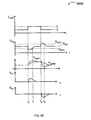
- FIG. 2B is a waveform diagram 200 B showing example operation of the regulator shown in FIG. 2A .
- the output load can increase from I 1 to I 2 , resulting in a dip in the output voltage, which is reflected at V FB .
- Linear amplifier output V COMP may respond slowly, but comparator 254 - 1 can generate a positive pulse V A1 to increase the duty cycle and quickly increase V OUT and V FB toward steady state values via more aggressive control signal V CONT .
- V FB can increase within the regulation band.
- the non-linear loop may gradually stop functioning, and the linear amplifier can maintain steady state regulation.
- the duration of such non-linear circuit 204 operation can be controlled by LIM 252 - 1 .
- comparator 254 - 2 and LIM 252 - 2 can perform a non-linear modulation function to quickly decrease V OUT and V FB toward steady state values via more aggressive control signal V CONT .
- outputs from LIM 252 - 1 (e.g., V A1 ) and LIM 252 - 2 (e.g., V A2 ) can be summed by summation circuit 250 to produce adjustment signal V ADJ .
- Limiting (LIM) circuits 252 can be any suitable circuitry for processing comparator 254 outputs (e.g., gain filters, time duration limiters, amplitude limiters, or other suitable limiters, etc.). Further, while this particular example uses only two thresholds and two comparators to realize a non-linear circuit, any suitable number (e.g., more than two thresholds and two comparators) can be used to further speed up the transient responses.
- FIG. 2C shown is a block schematic diagram 204 C of a first example non-linear circuit in accordance with embodiments of the present invention.
- This approach represents a digital based implementation of non-linear circuit 204 .
- an error signal between FB and regulation reference V REF can be sampled (e.g., via transconductance amplifier 260 and resistor R X ) and converted into a digital signal (e.g., via analog-to-digital (A/D) converter 262 ).
- Digital filter 264 may then be used to process a digital output from A/D converter 262 to calculate adjustment signal V ADJ-D .
- V ADJ-D may be converted back to an analog signal (e.g., via digital-to-analog (D/A) converter 266 ) to provide V ADJ for summation with a linear amplifier output for PWM control.
- digital signal V ADJ-D may be fed into driver logic (e.g., 108 ) to supplement control signal PWM for active switch (e.g., M 1 and M 2 ) duty cycle modulation in some control architectures.
- digital filter 264 can be programmed or reconfigured by user interface control.
- non-linear circuit 204 can be implemented using multiple amplifiers.
- Amplifier 290 can be used to amplify a difference between FB and first threshold V REF1 to adjust control signal V CONT into PWM control/drive block 150 .
- Amplifier 292 can be used to amplify a difference between FB and second threshold V REF2 to adjust control signal V CONT into PWM control/drive block 150 .
- outputs from amplifiers 290 and 292 can be combined via summation circuit 294 to provide adjustment signal V ADJ .
- any suitable number of amplifiers and thresholds e.g., more than two amplifiers with different transfer functions and more than two thresholds) can be used to further optimize stability and transient responses.
- a multiple output switching regulator controller includes: (i) a power stage that powers a plurality of loads at a corresponding plurality of output terminals by converting an input signal; and (ii) a first feedback circuit that amplifies an output regulation difference between each output terminal and a corresponding regulation reference using time division multiplexing (TDM), where the first feedback circuit generates a plurality of control signals corresponding to each output terminal, and each control signal is generated during a predetermined time interval using TDM, and each control signal is held until a next sensing interval. Also, each control signal controls the switching regulator to match each output terminal to the corresponding regulation reference during a steady state operation of the switching regulator.
- the first feedback circuit uses a linear circuit (e.g., linear amplifiers), but the first feedback circuit can also be a non-linear circuit including comparators, or a sum of both linear and non-linear circuits.
- FIG. 3A shown is a block schematic diagram 300 A of an example regulator for two outputs in accordance with embodiments of the present invention.
- This particular arrangement of non-linear circuit 204 can effectively increase a transient response speed in the multi-output regulator while minimizing hardware overhead by sharing the relatively slow response circuitry.
- output loops for OUT 1 e.g., including non-linear circuit 204 - 1 , summation circuit 206 - 1 , and PWM control/drive 150 - 1 for controlling active switches M 11 and M 21
- OUT 2 e.g., including non-linear circuit 204 - 2 , summation circuit 206 - 2 , and PWM control/drive 150 - 2 for controlling active switches M 12 and M 22
- OUT 1 e.g., including non-linear circuit 204 - 1 , summation circuit 206 - 1 , and PWM control/drive 150 - 1 for controlling active switches M 11 and M 21
- OUT 2 e.g., including non-linear circuit 204 - 2 , summation circuit 206 - 2 , and PWM control/drive 150 - 2 for controlling active switches M 12 and M 22
- OUT 1 e.g., including non-linear circuit 204 - 1 , summation circuit 206 - 1 , and
- time division multiplexing may be used (e.g., via time division controller 310 ) to generate a DC error signal for each output (e.g., OUT 1 and OUT 2 ) by multiplexing inputs (e.g., FB 1 and FB 2 ) and outputs of the common error amplifiers among different channels.
- TDM time division multiplexing
- MUX 306 can connect a transconductance amplifier 304 output to a first compensation capacitor C C1 , thus integrating an error between FB 1 and regulation reference V REF via MUX 308 .
- MUX 306 can connect a transconductance amplifier 304 output to a second compensation capacitor C C2 , thus integrating an error between FB 2 and V REF via MUX 308 .
- Voltages (e.g., V COMP1 and V COMP2 ) on each compensation capacitor can then be used to achieve proper steady state regulation on the corresponding output (e.g., OUT 1 and OUT 2 ).
- non-linear circuits 204 can sense a corresponding output voltage, and modulate a voltage (e.g., V ADJ1 and V ADJ2 ) to generate a relatively fast control voltage (e.g., V CONT1 and V CONT2 ) in order to change the duty cycle of the associated power stage and achieve good output transient response.
- a voltage e.g., V ADJ1 and V ADJ2
- V CONT1 and V CONT2 relatively fast control voltage
- FIG. 3B shown is a block schematic diagram 300 B of a first example regulator for N outputs in accordance with embodiments of the present invention.
- This example regulator can include power stage 320 (e.g., active switches M 1 and M 2 , inductors, etc.), common linear amplifier 302 , PWM control/drive 150 for each output channel (e.g., for OUT 1 , OUT 2 , . . . OUT N ), and non-linear circuit 204 for each channel.
- power stage 320 e.g., active switches M 1 and M 2 , inductors, etc.
- PWM control/drive 150 for each output channel (e.g., for OUT 1 , OUT 2 , . . . OUT N ), and non-linear circuit 204 for each channel.
- non-linear control can also be shared among all channels (e.g., 1, 2, . . . N) with suitable time division and multiplexing switches MUX 330 and MUX 334 , as well as EA 332 .
- common block 350 can include various types of circuitry.
- common feedback control 340 can include both linear amplifiers (e.g., for DC regulation), as well as non-linear circuitry (e.g., for transient/AC operation).
- linear amplifiers e.g., for DC regulation
- non-linear circuitry e.g., for transient/AC operation.
- FIG. 3D may be best suited for relatively low-cost applications whereby TDM can be used for both DC (steady state) and AC (transient) regulation because transient response times may not be quite as critical.
- the time division circuits as discussed herein can divide one sense period into multiple time durations for common sub-circuits to be adapted to each output channel having a same duration.
- the sense period can be one switching cycle, divided into a same number of time intervals as the number of output channels.
- the sense period can also include multiple switching periods when the common sub-circuits are adapted to one output channel in one switching period. Particular embodiments are also amenable to other ways to divide the sense period, depending on the application requirements.
- a method of controlling a switching regulator includes: (i) amplifying a regulation difference between an output terminal and a regulation reference using a first feedback circuit; (ii) generating a control signal from the amplified difference for steady state operation of the switching regulator; (iii) sensing the regulation difference between the output terminal and the regulation reference using a second feedback circuit; and (iv) generating an adjustment signal for adjusting the control signal under transient conditions to improve a transient response of the switching regulator.
- FIG. 4A shown is a flow diagram 400 A of an example method of controlling a switching regulator in accordance with embodiments of the present invention.
- the flow begins ( 402 ), and a regulation difference between an output terminal and a regulation reference can be amplified ( 404 ), such as via EA 208 .
- a control signal e.g., V CONT
- V CONT can then be generated from the amplified difference for steady state operation ( 406 ).
- the regulation difference can also be sensed using a different feedback circuit ( 408 ), such as non-linear circuit 204 .
- An adjustment signal e.g., V ADJ
- V ADJ can then be generated to adjust the control signal for transient operation ( 410 ), completing the flow ( 412 ).
- a method of controlling a multiple output switching regulator includes: (i) dividing a sensing period into a plurality of time intervals; (ii) amplifying an output regulation difference between each of a plurality of output terminals and a corresponding regulation reference using a first common feedback circuit; (iii) generating a corresponding control signal in a corresponding time intervals, where the corresponding control signal is held until a next sensing interval; and (iv) using each control signal to produce a stable output level at the corresponding output terminal to match the corresponding regulation reference during steady state operation.
- FIG. 4B shown is a flow diagram 400 B of an example method of controlling a multiple output switching regulator in accordance with embodiments of the present invention.
- the flow can begin ( 452 ), and a sensing period can be divided into time intervals ( 454 ), such as via time division controller 310 .
- An output regulation difference between output terminals and corresponding regulation references can be amplified ( 456 ), such as via transconductance amplifier 304 .
- a corresponding control signal (e.g., V CONT1 , V CONT2 , . . . V CONTN ) can be generated for a given time interval ( 458 ).
- Each control signal can then be used to produce a stable output level at each output terminal (e.g., OUT 1 , OUT 2 , . . . OUT N ) during steady state operation ( 460 ), completing the flow ( 462 ).
- regulators employ an inductor-based switching regulator topology.
- any suitable type of regulator e.g., linear regulators, transformer-based switching regulators, charge pump regulator circuit topologies, boost regulator, buck-boost, flyback, etc.
- particular amplifiers e.g., linear amplifiers
- other types of amplifiers such as digital amplifiers
- control methods in circuitry described herein can be applied to regulators with any output signals (e.g., constant current, AC voltage, AC current), as opposed to strictly being applied to constant voltage applications.
- an input voltage can range from about 2.5 V to about 5.5 V, such as from about 2.7 to about 4.2 V, and including about 4.2 V.
- Regulated output voltages in such a step down regulator example can range from about 0.8 V to abut 2.2 V, and including from about 1 V to about 1.8 V, and more specifically about 1.5 V.
- some such voltages can apply in a cell phone application, and can be utilized for main chip power, random-access memory (RAM) power, or the like.
Landscapes
- Engineering & Computer Science (AREA)
- Power Engineering (AREA)
- Dc-Dc Converters (AREA)
Abstract
Description
Claims (20)
Priority Applications (4)
| Application Number | Priority Date | Filing Date | Title |
|---|---|---|---|
| US12/455,978 US8749213B2 (en) | 2009-06-09 | 2009-06-09 | Mixed mode control for switching regulator with fast transient responses |
| CN201010123581XA CN101800474B (en) | 2009-06-09 | 2010-03-12 | Switching type adjustor controller and mixed mode controlling method thereof |
| TW099109647A TWI479788B (en) | 2009-06-09 | 2010-03-30 | Switching regulator controller and method of controlling switching regulator |
| US14/256,186 US20140232190A1 (en) | 2009-06-09 | 2014-04-18 | Mixed mode control for switching regulator with fast transient responses |
Applications Claiming Priority (1)
| Application Number | Priority Date | Filing Date | Title |
|---|---|---|---|
| US12/455,978 US8749213B2 (en) | 2009-06-09 | 2009-06-09 | Mixed mode control for switching regulator with fast transient responses |
Related Child Applications (1)
| Application Number | Title | Priority Date | Filing Date |
|---|---|---|---|
| US14/256,186 Continuation US20140232190A1 (en) | 2009-06-09 | 2014-04-18 | Mixed mode control for switching regulator with fast transient responses |
Publications (2)
| Publication Number | Publication Date |
|---|---|
| US20100308654A1 US20100308654A1 (en) | 2010-12-09 |
| US8749213B2 true US8749213B2 (en) | 2014-06-10 |
Family
ID=42596012
Family Applications (2)
| Application Number | Title | Priority Date | Filing Date |
|---|---|---|---|
| US12/455,978 Active 2031-07-29 US8749213B2 (en) | 2009-06-09 | 2009-06-09 | Mixed mode control for switching regulator with fast transient responses |
| US14/256,186 Abandoned US20140232190A1 (en) | 2009-06-09 | 2014-04-18 | Mixed mode control for switching regulator with fast transient responses |
Family Applications After (1)
| Application Number | Title | Priority Date | Filing Date |
|---|---|---|---|
| US14/256,186 Abandoned US20140232190A1 (en) | 2009-06-09 | 2014-04-18 | Mixed mode control for switching regulator with fast transient responses |
Country Status (3)
| Country | Link |
|---|---|
| US (2) | US8749213B2 (en) |
| CN (1) | CN101800474B (en) |
| TW (1) | TWI479788B (en) |
Cited By (12)
| Publication number | Priority date | Publication date | Assignee | Title |
|---|---|---|---|---|
| US20130147457A1 (en) * | 2011-12-13 | 2013-06-13 | Korea University Research And Business Foundation | Single inductor multiple output (simo) direct current-to-direct current (dc/dc) converter and control method thereof |
| US20140232190A1 (en) * | 2009-06-09 | 2014-08-21 | Silergy Semiconductor Technology (Hangzhou) Ltd | Mixed mode control for switching regulator with fast transient responses |
| US20160359413A1 (en) * | 2015-06-05 | 2016-12-08 | Endura IP Holdings Ltd. | Voltage regulator current load sensing |
| US9660538B2 (en) * | 2015-05-06 | 2017-05-23 | Switching Power, Inc. | Digital closed-loop control for DC/DC switch-mode power converters with multiple outputs |
| US20170194857A1 (en) * | 2015-12-31 | 2017-07-06 | Silergy Semiconductor Technology (Hangzhou) Ltd | Voltage regulation circuit of single inductor and multiple outputs and control method |
| US20170255214A1 (en) * | 2016-03-02 | 2017-09-07 | Qualcomm Incorporated | Multiple input multiple output regulator controller system |
| US20180227849A1 (en) * | 2017-02-06 | 2018-08-09 | Itron Networked Solutions, Inc. | Battery control for safeguarding lower voltage integrated circuits |
| US10110124B2 (en) | 2016-05-18 | 2018-10-23 | Silergy Semiconductor Technology (Hangzhou) Ltd | Control circuit and control method for switching regulator and switching regulator with the same |
| US10194497B2 (en) | 2016-05-27 | 2019-01-29 | Silergy Semiconductor Technology (Hangzhou) Ltd | Control circuit, control method and switching power supply thereof |
| US20200076299A1 (en) * | 2018-08-30 | 2020-03-05 | Qualcomm Incorporated | Switched common-mode current control for single-inductor-multiple-output (simo) power converters |
| US11050432B2 (en) | 2019-04-24 | 2021-06-29 | Silergy Semiconductor Technology (Hangzhou) Ltd | Pseudo differential analog-to-digital converter |
| US11909301B2 (en) | 2020-09-15 | 2024-02-20 | Silergy Semiconductor Technology (Hangzhou) Co., Ltd. | Switching power supply and intermittent power saving mode control circuit and method thereof |
Families Citing this family (110)
| Publication number | Priority date | Publication date | Assignee | Title |
|---|---|---|---|---|
| US9112452B1 (en) | 2009-07-14 | 2015-08-18 | Rf Micro Devices, Inc. | High-efficiency power supply for a modulated load |
| US8624429B2 (en) * | 2009-07-20 | 2014-01-07 | The Hong Kong University Of Science And Technology | Single-inductor-multiple-output regulator with auto-hopping control and the method of use |
| US8643349B2 (en) * | 2009-11-09 | 2014-02-04 | Semiconductor Components Industries, Llc | Power supply controller and method |
| US9035633B1 (en) * | 2009-12-29 | 2015-05-19 | Sunpower Corporation | Switching power converter control |
| US8575910B2 (en) * | 2010-01-20 | 2013-11-05 | Intersil Americas Inc. | Single-cycle charge regulator for digital control |
| US8633766B2 (en) | 2010-04-19 | 2014-01-21 | Rf Micro Devices, Inc. | Pseudo-envelope follower power management system with high frequency ripple current compensation |
| US9431974B2 (en) | 2010-04-19 | 2016-08-30 | Qorvo Us, Inc. | Pseudo-envelope following feedback delay compensation |
| US8981848B2 (en) | 2010-04-19 | 2015-03-17 | Rf Micro Devices, Inc. | Programmable delay circuitry |
| EP3376667B1 (en) | 2010-04-19 | 2021-07-28 | Qorvo US, Inc. | Pseudo-envelope following power management system |
| US9099961B2 (en) | 2010-04-19 | 2015-08-04 | Rf Micro Devices, Inc. | Output impedance compensation of a pseudo-envelope follower power management system |
| US8519788B2 (en) | 2010-04-19 | 2013-08-27 | Rf Micro Devices, Inc. | Boost charge-pump with fractional ratio and offset loop for supply modulation |
| US8866549B2 (en) | 2010-06-01 | 2014-10-21 | Rf Micro Devices, Inc. | Method of power amplifier calibration |
| US8461897B2 (en) | 2010-06-07 | 2013-06-11 | Skyworks Solutions, Inc. | Apparatus and method for well buffering |
| US8441149B2 (en) | 2010-06-25 | 2013-05-14 | Intel Corporation | Distributed power delivery scheme for on-die voltage scaling |
| US8571498B2 (en) | 2010-08-25 | 2013-10-29 | Rf Micro Devices, Inc. | Multi-mode/multi-band power management system |
| EP2434363B1 (en) * | 2010-09-27 | 2013-05-15 | ST-Ericsson SA | Presence and operability test of a decoupling capacitor |
| WO2012047738A1 (en) | 2010-09-29 | 2012-04-12 | Rf Micro Devices, Inc. | SINGLE μC-BUCKBOOST CONVERTER WITH MULTIPLE REGULATED SUPPLY OUTPUTS |
| US9075673B2 (en) | 2010-11-16 | 2015-07-07 | Rf Micro Devices, Inc. | Digital fast dB to gain multiplier for envelope tracking systems |
| TWI479780B (en) * | 2010-12-13 | 2015-04-01 | Hon Hai Prec Ind Co Ltd | Synchronous buck converter |
| US8588713B2 (en) | 2011-01-10 | 2013-11-19 | Rf Micro Devices, Inc. | Power management system for multi-carriers transmitter |
| US8611402B2 (en) | 2011-02-02 | 2013-12-17 | Rf Micro Devices, Inc. | Fast envelope system calibration |
| US8624760B2 (en) | 2011-02-07 | 2014-01-07 | Rf Micro Devices, Inc. | Apparatuses and methods for rate conversion and fractional delay calculation using a coefficient look up table |
| EP2673880B1 (en) | 2011-02-07 | 2017-09-06 | Qorvo US, Inc. | Group delay calibration method for power amplifier envelope tracking |
| US20120229107A1 (en) * | 2011-03-11 | 2012-09-13 | Intersil Americas Inc. | System and method for current sensing within a voltage regulator |
| US9614094B2 (en) * | 2011-04-29 | 2017-04-04 | Semiconductor Energy Laboratory Co., Ltd. | Semiconductor device including oxide semiconductor layer and method for driving the same |
| US9379667B2 (en) | 2011-05-05 | 2016-06-28 | Rf Micro Devices, Inc. | Multiple power supply input parallel amplifier based envelope tracking |
| US9246460B2 (en) | 2011-05-05 | 2016-01-26 | Rf Micro Devices, Inc. | Power management architecture for modulated and constant supply operation |
| US9247496B2 (en) | 2011-05-05 | 2016-01-26 | Rf Micro Devices, Inc. | Power loop control based envelope tracking |
| CN103748794B (en) | 2011-05-31 | 2015-09-16 | 射频小型装置公司 | A kind of method and apparatus of the complex gain for measuring transmission path |
| US9019011B2 (en) | 2011-06-01 | 2015-04-28 | Rf Micro Devices, Inc. | Method of power amplifier calibration for an envelope tracking system |
| US8760228B2 (en) | 2011-06-24 | 2014-06-24 | Rf Micro Devices, Inc. | Differential power management and power amplifier architecture |
| US8952710B2 (en) | 2011-07-15 | 2015-02-10 | Rf Micro Devices, Inc. | Pulsed behavior modeling with steady state average conditions |
| US8792840B2 (en) | 2011-07-15 | 2014-07-29 | Rf Micro Devices, Inc. | Modified switching ripple for envelope tracking system |
| US8626091B2 (en) | 2011-07-15 | 2014-01-07 | Rf Micro Devices, Inc. | Envelope tracking with variable compression |
| US9263996B2 (en) | 2011-07-20 | 2016-02-16 | Rf Micro Devices, Inc. | Quasi iso-gain supply voltage function for envelope tracking systems |
| US8618868B2 (en) | 2011-08-17 | 2013-12-31 | Rf Micro Devices, Inc. | Single charge-pump buck-boost for providing independent voltages |
| WO2013033700A1 (en) | 2011-09-02 | 2013-03-07 | Rf Micro Devices, Inc. | Split vcc and common vcc power management architecture for envelope tracking |
| US8957728B2 (en) | 2011-10-06 | 2015-02-17 | Rf Micro Devices, Inc. | Combined filter and transconductance amplifier |
| CN102355131B (en) * | 2011-10-14 | 2014-01-29 | 矽力杰半导体技术(杭州)有限公司 | Hybrid control method and device of four-switch Buck-Boost converter |
| CN103959189B (en) | 2011-10-26 | 2015-12-23 | 射频小型装置公司 | Based on the parallel amplifier phase compensation of inductance |
| US9484797B2 (en) | 2011-10-26 | 2016-11-01 | Qorvo Us, Inc. | RF switching converter with ripple correction |
| CN103988406B (en) | 2011-10-26 | 2017-03-01 | Qorvo美国公司 | Radio frequency (RF) switching converter and RF amplifying device using the RF switching converter |
| US9024688B2 (en) | 2011-10-26 | 2015-05-05 | Rf Micro Devices, Inc. | Dual parallel amplifier based DC-DC converter |
| US8975959B2 (en) | 2011-11-30 | 2015-03-10 | Rf Micro Devices, Inc. | Monotonic conversion of RF power amplifier calibration data |
| US9515621B2 (en) | 2011-11-30 | 2016-12-06 | Qorvo Us, Inc. | Multimode RF amplifier system |
| US9250643B2 (en) | 2011-11-30 | 2016-02-02 | Rf Micro Devices, Inc. | Using a switching signal delay to reduce noise from a switching power supply |
| US8947161B2 (en) | 2011-12-01 | 2015-02-03 | Rf Micro Devices, Inc. | Linear amplifier power supply modulation for envelope tracking |
| US9041365B2 (en) | 2011-12-01 | 2015-05-26 | Rf Micro Devices, Inc. | Multiple mode RF power converter |
| US9280163B2 (en) | 2011-12-01 | 2016-03-08 | Rf Micro Devices, Inc. | Average power tracking controller |
| US9256234B2 (en) | 2011-12-01 | 2016-02-09 | Rf Micro Devices, Inc. | Voltage offset loop for a switching controller |
| WO2013082384A1 (en) | 2011-12-01 | 2013-06-06 | Rf Micro Devices, Inc. | Rf power converter |
| US9494962B2 (en) | 2011-12-02 | 2016-11-15 | Rf Micro Devices, Inc. | Phase reconfigurable switching power supply |
| US9813036B2 (en) | 2011-12-16 | 2017-11-07 | Qorvo Us, Inc. | Dynamic loadline power amplifier with baseband linearization |
| US9298198B2 (en) | 2011-12-28 | 2016-03-29 | Rf Micro Devices, Inc. | Noise reduction for envelope tracking |
| US8432140B1 (en) * | 2012-02-13 | 2013-04-30 | Microchip Technology Incorporated | Dual mode boost regulator |
| JP6227890B2 (en) | 2012-05-02 | 2017-11-08 | 株式会社半導体エネルギー研究所 | Signal processing circuit and control circuit |
| US8981839B2 (en) | 2012-06-11 | 2015-03-17 | Rf Micro Devices, Inc. | Power source multiplexer |
| US9136760B2 (en) | 2012-06-27 | 2015-09-15 | Analog Devices Global | Digital switched mode voltage regulator |
| CN103580450B (en) * | 2012-07-20 | 2017-03-29 | 中兴通讯股份有限公司 | A kind of circuit for realizing parallel electric source module automatic current equalizing in proportion |
| WO2014018861A1 (en) * | 2012-07-26 | 2014-01-30 | Rf Micro Devices, Inc. | Programmable rf notch filter for envelope tracking |
| US9225231B2 (en) | 2012-09-14 | 2015-12-29 | Rf Micro Devices, Inc. | Open loop ripple cancellation circuit in a DC-DC converter |
| US9197256B2 (en) | 2012-10-08 | 2015-11-24 | Rf Micro Devices, Inc. | Reducing effects of RF mixer-based artifact using pre-distortion of an envelope power supply signal |
| WO2014062902A1 (en) | 2012-10-18 | 2014-04-24 | Rf Micro Devices, Inc | Transitioning from envelope tracking to average power tracking |
| US10013003B2 (en) | 2012-11-16 | 2018-07-03 | Linear Technology Corporation | Feed forward current mode switching regulator with improved transient response |
| US9627975B2 (en) | 2012-11-16 | 2017-04-18 | Qorvo Us, Inc. | Modulated power supply system and method with automatic transition between buck and boost modes |
| US9929696B2 (en) | 2013-01-24 | 2018-03-27 | Qorvo Us, Inc. | Communications based adjustments of an offset capacitive voltage |
| US9178472B2 (en) | 2013-02-08 | 2015-11-03 | Rf Micro Devices, Inc. | Bi-directional power supply signal based linear amplifier |
| US9348383B2 (en) * | 2013-03-01 | 2016-05-24 | Intel Corporation | Apparatus for starting up switching voltage regulator |
| WO2014152876A1 (en) | 2013-03-14 | 2014-09-25 | Rf Micro Devices, Inc | Noise conversion gain limited rf power amplifier |
| WO2014152903A2 (en) | 2013-03-14 | 2014-09-25 | Rf Micro Devices, Inc | Envelope tracking power supply voltage dynamic range reduction |
| US9696350B2 (en) * | 2013-03-15 | 2017-07-04 | Intel Corporation | Non-linear control for voltage regulator |
| CN103199700B (en) * | 2013-03-22 | 2015-08-12 | 成都芯源系统有限公司 | Buck-boost converter and controller and control method thereof |
| US9479118B2 (en) | 2013-04-16 | 2016-10-25 | Rf Micro Devices, Inc. | Dual instantaneous envelope tracking |
| CN103389767A (en) * | 2013-07-08 | 2013-11-13 | 郑儒富 | Constant current driver and control method thereof |
| US9374005B2 (en) | 2013-08-13 | 2016-06-21 | Rf Micro Devices, Inc. | Expanded range DC-DC converter |
| US9203309B2 (en) * | 2013-09-11 | 2015-12-01 | Qualcomm, Incorporated | Multi-output boost regulator with single control loop |
| US9490629B1 (en) * | 2013-09-18 | 2016-11-08 | Volterra Semiconductor LLC | DC-to-DC converter controllers including over-current protection, and associated systems and methods |
| CN103546019B (en) * | 2013-10-16 | 2015-12-09 | 华南理工大学 | The energy balance controller of converters and method |
| CN104734265B (en) * | 2013-12-24 | 2017-11-03 | 华硕电脑股份有限公司 | Battery charging circuit and battery charging method |
| EP3090481A1 (en) * | 2013-12-30 | 2016-11-09 | Telefonaktiebolaget LM Ericsson (publ) | Voltage range determination for an intermediate bus architecture power supply controller |
| CN104753346B (en) * | 2013-12-30 | 2017-05-24 | 展讯通信(上海)有限公司 | Technology for improving efficiency of BUCK circuit |
| CN104753345A (en) * | 2013-12-30 | 2015-07-01 | 展讯通信(上海)有限公司 | Technology for improving transient response of BUCK circuit |
| CN103683923B (en) * | 2014-01-03 | 2015-12-09 | 东南大学 | A Control Circuit of Single Inductor Four Output Step-Down Switching Power Supply |
| US9614476B2 (en) | 2014-07-01 | 2017-04-04 | Qorvo Us, Inc. | Group delay calibration of RF envelope tracking |
| CN104377945B (en) * | 2014-11-21 | 2016-12-28 | 成都芯源系统有限公司 | Reference signal generating circuit and method thereof |
| US9843294B2 (en) | 2015-07-01 | 2017-12-12 | Qorvo Us, Inc. | Dual-mode envelope tracking power converter circuitry |
| US9912297B2 (en) | 2015-07-01 | 2018-03-06 | Qorvo Us, Inc. | Envelope tracking power converter circuitry |
| WO2017137996A1 (en) | 2016-02-10 | 2017-08-17 | B. G. Negev Technologies And Applications Ltd., At Ben-Gurion University | Plug-and-play electronic capacitor for voltage regulator modules applications |
| US9973147B2 (en) | 2016-05-10 | 2018-05-15 | Qorvo Us, Inc. | Envelope tracking power management circuit |
| CN107666241A (en) * | 2016-07-30 | 2018-02-06 | 智瑞佳(苏州)半导体科技有限公司 | A kind of digital DC D/C powers conversion chip and its control method |
| US10250252B2 (en) * | 2016-11-03 | 2019-04-02 | Semiconductor Components Industries, Llc | Control circuit and method therefor |
| JP6774884B2 (en) * | 2017-01-27 | 2020-10-28 | 富士通株式会社 | Power supply device and control method of power supply device |
| CN109997302B (en) * | 2017-02-09 | 2021-09-17 | 密克罗奇普技术公司 | Circuit and method for controlling a switched mode power supply |
| CN207603443U (en) * | 2017-09-21 | 2018-07-10 | 北京比特大陆科技有限公司 | It calculates power plate power stage circuit, packaging power device and calculates power plate |
| CN108183596B (en) * | 2017-12-21 | 2020-08-25 | 成都芯源系统有限公司 | DC converter and method thereof |
| EP3514930A1 (en) * | 2018-01-23 | 2019-07-24 | IDT Europe GmbH | Method to optimally control dead times of a synchronous buck converter |
| CN108566074B (en) * | 2018-02-05 | 2019-07-19 | 东莞市紫能电子科技有限公司 | A kind of power supply device and its control method with two-way output |
| JP6592126B2 (en) | 2018-02-09 | 2019-10-16 | 華邦電子股▲ふん▼有限公司Winbond Electronics Corp. | Bit line power supply device |
| TWI662390B (en) * | 2018-03-01 | 2019-06-11 | 新唐科技股份有限公司 | Digital control system for voltage regulation and method thereof |
| US10476437B2 (en) | 2018-03-15 | 2019-11-12 | Qorvo Us, Inc. | Multimode voltage tracker circuit |
| US10389236B1 (en) | 2018-03-29 | 2019-08-20 | Psemi Corporation | Disturbance quelling |
| US10666139B1 (en) * | 2019-02-27 | 2020-05-26 | Analog Devices International Unlimited Company | Switching regulator with proportional-integral (PI) control compensation network clamp |
| CN114830517A (en) * | 2019-12-17 | 2022-07-29 | 罗姆股份有限公司 | Output feedback control circuit |
| WO2021187053A1 (en) * | 2020-03-17 | 2021-09-23 | ローム株式会社 | Output feedback control circuit and switching power supply |
| US11258364B2 (en) * | 2020-04-09 | 2022-02-22 | High Tech Technology Limited | Flexible array of DC-DC converters reconfigurable using a shared serial bus |
| CN111551811A (en) * | 2020-05-26 | 2020-08-18 | 无锡友达电子有限公司 | A detection circuit, device and charging equipment for output state of charging equipment |
| WO2022015242A1 (en) * | 2020-07-16 | 2022-01-20 | Zero-Error Systems Pte. Ltd. | A device and method for charging energy storage devices |
| CN112104229B (en) * | 2020-09-25 | 2021-10-12 | 深圳南云微电子有限公司 | BUCK control circuit, control method and reference generation circuit |
| CN115250068A (en) * | 2021-04-27 | 2022-10-28 | 海信视像科技股份有限公司 | Multiplex feedback method, circuit and display device |
| CN121239006A (en) * | 2025-11-28 | 2025-12-30 | 深圳市微源半导体股份有限公司 | Boost converter, transient response circuit thereof and control method |
Citations (15)
| Publication number | Priority date | Publication date | Assignee | Title |
|---|---|---|---|---|
| US5003454A (en) * | 1990-01-09 | 1991-03-26 | North American Philips Corporation | Power supply with improved power factor correction |
| US5617015A (en) * | 1995-06-07 | 1997-04-01 | Linear Technology Corporation | Multiple output regulator with time sequencing |
| US6249447B1 (en) * | 1999-08-13 | 2001-06-19 | Tyco Electronics Logistics Ag | System and method for determining output current and converter employing the same |
| US6437545B2 (en) * | 2000-07-06 | 2002-08-20 | Koninklijke Philips Electronics N.V. | DC/DC converter including control means for controlling multiple outputs using separate switching cycles for each output |
| US20020180410A1 (en) * | 2000-11-07 | 2002-12-05 | Brooks Steven W. | Switching regulator with transient recovery circuit |
| US6756771B1 (en) * | 2003-06-20 | 2004-06-29 | Semiconductor Components Industries, L.L.C. | Power factor correction method with zero crossing detection and adjustable stored reference voltage |
| US20050007083A1 (en) * | 2003-07-10 | 2005-01-13 | Ta-Yung Yang | Power supply having multi-vector error amplifier for power factor correction |
| US20050110474A1 (en) * | 2003-11-24 | 2005-05-26 | Ortiz Joe A. | Method for input current regulation and active-power filter with input voltage feedforward and output load feedforward |
| US20080231115A1 (en) * | 2007-03-16 | 2008-09-25 | Gyuha Cho | Multiple-Output DC-DC Converter |
| US20080238396A1 (en) | 2007-03-30 | 2008-10-02 | Hong Kong Applied Science and Technology Research Institute Company Limited | Feedback controller having multiple feedback paths |
| US20080297128A1 (en) * | 2007-05-31 | 2008-12-04 | Texas Instruments Incorporated | Sample and hold scheme for a feedback network of a power converter |
| US20080303501A1 (en) * | 2004-10-01 | 2008-12-11 | Aleksandar Prodic | Digital Controller for Dc-Dc Switching Converters for Operation at Ultra-High Constant Switching Frequencies |
| US7508176B2 (en) * | 2004-05-14 | 2009-03-24 | O2Micro International Limited | Controller for a DC to DC converter having linear mode and switch mode capabilities |
| US20090212751A1 (en) * | 2006-03-06 | 2009-08-27 | Pedro Alou Cervera | Controller for a Power Converter and Method of Operating The Same |
| US8049472B2 (en) * | 2008-07-29 | 2011-11-01 | Cosmic Circuits Private Limited | Single inductor multiple output switching devices |
Family Cites Families (6)
| Publication number | Priority date | Publication date | Assignee | Title |
|---|---|---|---|---|
| JP3688676B2 (en) * | 2002-11-14 | 2005-08-31 | ローム株式会社 | Switching power supply device and controller IC thereof |
| JP4619822B2 (en) * | 2005-03-03 | 2011-01-26 | 株式会社リコー | Switching regulator and voltage control method thereof |
| US7141956B2 (en) * | 2005-03-18 | 2006-11-28 | Power-One, Inc. | Digital output voltage regulation circuit having first control loop for high speed and second control loop for high accuracy |
| GB2429351B (en) * | 2005-08-17 | 2009-07-08 | Wolfson Microelectronics Plc | Feedback controller for PWM amplifier |
| US8749213B2 (en) * | 2009-06-09 | 2014-06-10 | Silergy Technology | Mixed mode control for switching regulator with fast transient responses |
| TWI448056B (en) * | 2010-06-14 | 2014-08-01 | Richtek Technology Corp | Adaptive constant on time adjustment circuit and method for adaptively adjusting constant on time |
-
2009
- 2009-06-09 US US12/455,978 patent/US8749213B2/en active Active
-
2010
- 2010-03-12 CN CN201010123581XA patent/CN101800474B/en active Active
- 2010-03-30 TW TW099109647A patent/TWI479788B/en active
-
2014
- 2014-04-18 US US14/256,186 patent/US20140232190A1/en not_active Abandoned
Patent Citations (15)
| Publication number | Priority date | Publication date | Assignee | Title |
|---|---|---|---|---|
| US5003454A (en) * | 1990-01-09 | 1991-03-26 | North American Philips Corporation | Power supply with improved power factor correction |
| US5617015A (en) * | 1995-06-07 | 1997-04-01 | Linear Technology Corporation | Multiple output regulator with time sequencing |
| US6249447B1 (en) * | 1999-08-13 | 2001-06-19 | Tyco Electronics Logistics Ag | System and method for determining output current and converter employing the same |
| US6437545B2 (en) * | 2000-07-06 | 2002-08-20 | Koninklijke Philips Electronics N.V. | DC/DC converter including control means for controlling multiple outputs using separate switching cycles for each output |
| US20020180410A1 (en) * | 2000-11-07 | 2002-12-05 | Brooks Steven W. | Switching regulator with transient recovery circuit |
| US6756771B1 (en) * | 2003-06-20 | 2004-06-29 | Semiconductor Components Industries, L.L.C. | Power factor correction method with zero crossing detection and adjustable stored reference voltage |
| US20050007083A1 (en) * | 2003-07-10 | 2005-01-13 | Ta-Yung Yang | Power supply having multi-vector error amplifier for power factor correction |
| US20050110474A1 (en) * | 2003-11-24 | 2005-05-26 | Ortiz Joe A. | Method for input current regulation and active-power filter with input voltage feedforward and output load feedforward |
| US7508176B2 (en) * | 2004-05-14 | 2009-03-24 | O2Micro International Limited | Controller for a DC to DC converter having linear mode and switch mode capabilities |
| US20080303501A1 (en) * | 2004-10-01 | 2008-12-11 | Aleksandar Prodic | Digital Controller for Dc-Dc Switching Converters for Operation at Ultra-High Constant Switching Frequencies |
| US20090212751A1 (en) * | 2006-03-06 | 2009-08-27 | Pedro Alou Cervera | Controller for a Power Converter and Method of Operating The Same |
| US20080231115A1 (en) * | 2007-03-16 | 2008-09-25 | Gyuha Cho | Multiple-Output DC-DC Converter |
| US20080238396A1 (en) | 2007-03-30 | 2008-10-02 | Hong Kong Applied Science and Technology Research Institute Company Limited | Feedback controller having multiple feedback paths |
| US20080297128A1 (en) * | 2007-05-31 | 2008-12-04 | Texas Instruments Incorporated | Sample and hold scheme for a feedback network of a power converter |
| US8049472B2 (en) * | 2008-07-29 | 2011-11-01 | Cosmic Circuits Private Limited | Single inductor multiple output switching devices |
Non-Patent Citations (2)
| Title |
|---|
| Dongsheng Ma, et al.; "A 1.8 V single-inductor dual-output switching converter for power reduction techniques," VLSI Circuits, 2001. Digest of Technical Papers. 2001 Symposium on,pp. 137-140. doi: 10.1109/VLSIC.2001.934219 URL: http://ieeexplore.ieee.org/stamp/stamp.jsp?tp=&arnumber=934219&isnumber=20220. * |
| Wing-Hung Ki; Dongsheng Ma; "Single-inductor multiple-output switching converters," Power Electronics Specialists Conference, 2001. PESC. 2001 IEEE 32nd Annual, vol. 1, pp. 226-231. doi: 10.1109/PESC.2001.954024 URL: http://ieeexplore.ieee.org/stamp/stamp.jsp?tp=&arnumber=954024&isnumber=20624. * |
Cited By (23)
| Publication number | Priority date | Publication date | Assignee | Title |
|---|---|---|---|---|
| US20140232190A1 (en) * | 2009-06-09 | 2014-08-21 | Silergy Semiconductor Technology (Hangzhou) Ltd | Mixed mode control for switching regulator with fast transient responses |
| US9007039B2 (en) * | 2011-12-13 | 2015-04-14 | Korea University Research And Business Foundation | Single inductor multiple output (SIMO) direct current-to-direct current (DC/DC) converter and control method thereof |
| US20130147457A1 (en) * | 2011-12-13 | 2013-06-13 | Korea University Research And Business Foundation | Single inductor multiple output (simo) direct current-to-direct current (dc/dc) converter and control method thereof |
| US9660538B2 (en) * | 2015-05-06 | 2017-05-23 | Switching Power, Inc. | Digital closed-loop control for DC/DC switch-mode power converters with multiple outputs |
| US10326364B2 (en) | 2015-06-05 | 2019-06-18 | Chaoyang Semiconductor Jiangyin Technology Co., Ltd. | Voltage regulator current load sensing |
| US20160359413A1 (en) * | 2015-06-05 | 2016-12-08 | Endura IP Holdings Ltd. | Voltage regulator current load sensing |
| US9673710B2 (en) * | 2015-06-05 | 2017-06-06 | Endura IP Holdings Ltd. | Voltage regulator current load sensing |
| US20170194857A1 (en) * | 2015-12-31 | 2017-07-06 | Silergy Semiconductor Technology (Hangzhou) Ltd | Voltage regulation circuit of single inductor and multiple outputs and control method |
| US11251700B2 (en) | 2015-12-31 | 2022-02-15 | Silergy Semiconductor Technology (Hangzhou) Ltd | Voltage regulation circuit of single inductor and multiple outputs and control method |
| US10348201B2 (en) * | 2015-12-31 | 2019-07-09 | Silergy Semiconductor Technology (Hangzhou) Ltd | Voltage regulation circuit of single inductor and multiple outputs and control method |
| US10627839B2 (en) * | 2016-03-02 | 2020-04-21 | Qualcomm Incorporated | Multiple input multiple output regulator controller system |
| US20170255214A1 (en) * | 2016-03-02 | 2017-09-07 | Qualcomm Incorporated | Multiple input multiple output regulator controller system |
| EP3423915B1 (en) * | 2016-03-02 | 2023-06-28 | Qualcomm Incorporated | Multiple input multiple output regulator controller system |
| US10110124B2 (en) | 2016-05-18 | 2018-10-23 | Silergy Semiconductor Technology (Hangzhou) Ltd | Control circuit and control method for switching regulator and switching regulator with the same |
| US10924010B2 (en) | 2016-05-18 | 2021-02-16 | Silergy Semiconductor Technology (Hangzhou) Ltd | Control circuit and control method for switching regulator and switching regulator with the same |
| US10194497B2 (en) | 2016-05-27 | 2019-01-29 | Silergy Semiconductor Technology (Hangzhou) Ltd | Control circuit, control method and switching power supply thereof |
| US10602577B2 (en) | 2016-05-27 | 2020-03-24 | Silergy Semiconductor Technology (Hangzhou) Ltd | Control circuit, control method and switching power supply thereof |
| US20180227849A1 (en) * | 2017-02-06 | 2018-08-09 | Itron Networked Solutions, Inc. | Battery control for safeguarding lower voltage integrated circuits |
| US11153819B2 (en) * | 2017-02-06 | 2021-10-19 | Itron Networked Solutions, Inc. | Battery control for safeguarding lower voltage integrated circuits |
| US20200076299A1 (en) * | 2018-08-30 | 2020-03-05 | Qualcomm Incorporated | Switched common-mode current control for single-inductor-multiple-output (simo) power converters |
| US10819233B2 (en) * | 2018-08-30 | 2020-10-27 | Qualcomm Incorporated | Switched common-mode current control for single-inductor-multiple-output (SIMO) power converters |
| US11050432B2 (en) | 2019-04-24 | 2021-06-29 | Silergy Semiconductor Technology (Hangzhou) Ltd | Pseudo differential analog-to-digital converter |
| US11909301B2 (en) | 2020-09-15 | 2024-02-20 | Silergy Semiconductor Technology (Hangzhou) Co., Ltd. | Switching power supply and intermittent power saving mode control circuit and method thereof |
Also Published As
| Publication number | Publication date |
|---|---|
| CN101800474A (en) | 2010-08-11 |
| US20100308654A1 (en) | 2010-12-09 |
| TW201108589A (en) | 2011-03-01 |
| TWI479788B (en) | 2015-04-01 |
| US20140232190A1 (en) | 2014-08-21 |
| CN101800474B (en) | 2012-06-27 |
Similar Documents
| Publication | Publication Date | Title |
|---|---|---|
| US8749213B2 (en) | Mixed mode control for switching regulator with fast transient responses | |
| US11251700B2 (en) | Voltage regulation circuit of single inductor and multiple outputs and control method | |
| US10250135B2 (en) | Fast response control circuit and control method thereof | |
| US8169205B2 (en) | Control for regulator fast transient response and low EMI noise | |
| US7923977B2 (en) | DC-DC converters with transient response control | |
| US10014780B2 (en) | Multiphase switching converter | |
| US8674669B2 (en) | Switching regulator with a single inductor in a multiple output power supply configuration | |
| Bondade et al. | A linear-assisted DC-DC hybrid power converter for envelope tracking RF power amplifiers | |
| US9755517B2 (en) | Multi-threshold panic comparators for multi-phase buck converter phase shedding control | |
| EP0993104A2 (en) | Capacitive-summing switch-mode power conversion control and method | |
| US8884598B2 (en) | Method and apparatus for operating a DC/DC converter | |
| US20190058398A1 (en) | Inductor current sensing and regulation for power converter | |
| US11804777B2 (en) | Power supply and emulated current mode control | |
| TW201439705A (en) | Switching regulator with adaptive PWM/PFM modulator and method thereof | |
| US20230063861A1 (en) | Control circuit, control chip and power supply device | |
| CN112019047B (en) | Automatic current sharing for power stages | |
| EP4164104B1 (en) | Power supply and emulated current mode control | |
| Su et al. | Pseudo-ramp current balance (PRCB) technique with offset cancellation control (OCC) in dual-phase DC-DC buck converter | |
| US8462937B2 (en) | Power supply with digital control loop | |
| TW202337118A (en) | Constant on time converter control circuit and constant on time converter | |
| US7688119B2 (en) | Power supply with digital control loop | |
| Ying et al. | A 95% efficiency Buck-Boost Converter with Full-Cycle Continuous Current Sensing and Adaptive Mode Control | |
| CN116742951B (en) | Switching power supply circuit and electronic device | |
| US20240250599A1 (en) | Low-power mode for multi-level converter | |
| US20240250612A1 (en) | Methods and Circuits for Constant On-Time Control of Switching Power Supplies |
Legal Events
| Date | Code | Title | Description |
|---|---|---|---|
| AS | Assignment |
Owner name: SILERGY TECHNOLOGY, CALIFORNIA Free format text: ASSIGNMENT OF ASSIGNORS INTEREST;ASSIGNOR:CHEN, WEI;REEL/FRAME:022853/0996 Effective date: 20090531 |
|
| AS | Assignment |
Owner name: SILERGY SEMICONDUCTOR TECHNOLOGY (HANGZHOU) LTD., Free format text: ASSIGNMENT OF ASSIGNORS INTEREST;ASSIGNOR:SILERGY TECHNOLOGY;REEL/FRAME:029201/0935 Effective date: 20121019 |
|
| STCF | Information on status: patent grant |
Free format text: PATENTED CASE |
|
| FEPP | Fee payment procedure |
Free format text: PAT HOLDER NO LONGER CLAIMS SMALL ENTITY STATUS, ENTITY STATUS SET TO UNDISCOUNTED (ORIGINAL EVENT CODE: STOL); ENTITY STATUS OF PATENT OWNER: LARGE ENTITY |
|
| MAFP | Maintenance fee payment |
Free format text: PAYMENT OF MAINTENANCE FEE, 4TH YEAR, LARGE ENTITY (ORIGINAL EVENT CODE: M1551) Year of fee payment: 4 |
|
| MAFP | Maintenance fee payment |
Free format text: PAYMENT OF MAINTENANCE FEE, 8TH YEAR, LARGE ENTITY (ORIGINAL EVENT CODE: M1552); ENTITY STATUS OF PATENT OWNER: LARGE ENTITY Year of fee payment: 8 |
|
| MAFP | Maintenance fee payment |
Free format text: PAYMENT OF MAINTENANCE FEE, 12TH YEAR, LARGE ENTITY (ORIGINAL EVENT CODE: M1553); ENTITY STATUS OF PATENT OWNER: LARGE ENTITY Year of fee payment: 12 |