WO2004102677A1 - Transparent conductive substrate for solar battery and method for producing same - Google Patents
Transparent conductive substrate for solar battery and method for producing same Download PDFInfo
- Publication number
- WO2004102677A1 WO2004102677A1 PCT/JP2004/006130 JP2004006130W WO2004102677A1 WO 2004102677 A1 WO2004102677 A1 WO 2004102677A1 JP 2004006130 W JP2004006130 W JP 2004006130W WO 2004102677 A1 WO2004102677 A1 WO 2004102677A1
- Authority
- WO
- WIPO (PCT)
- Prior art keywords
- layer
- transparent conductive
- substrate
- conductive substrate
- layers
- Prior art date
- Legal status (The legal status is an assumption and is not a legal conclusion. Google has not performed a legal analysis and makes no representation as to the accuracy of the status listed.)
- Ceased
Links
Classifications
-
- C—CHEMISTRY; METALLURGY
- C03—GLASS; MINERAL OR SLAG WOOL
- C03C—CHEMICAL COMPOSITION OF GLASSES, GLAZES OR VITREOUS ENAMELS; SURFACE TREATMENT OF GLASS; SURFACE TREATMENT OF FIBRES OR FILAMENTS MADE FROM GLASS, MINERALS OR SLAGS; JOINING GLASS TO GLASS OR OTHER MATERIALS
- C03C17/00—Surface treatment of glass, not in the form of fibres or filaments, by coating
- C03C17/34—Surface treatment of glass, not in the form of fibres or filaments, by coating with at least two coatings having different compositions
- C03C17/3411—Surface treatment of glass, not in the form of fibres or filaments, by coating with at least two coatings having different compositions with at least two coatings of inorganic materials
- C03C17/3417—Surface treatment of glass, not in the form of fibres or filaments, by coating with at least two coatings having different compositions with at least two coatings of inorganic materials all coatings being oxide coatings
-
- H—ELECTRICITY
- H10—SEMICONDUCTOR DEVICES; ELECTRIC SOLID-STATE DEVICES NOT OTHERWISE PROVIDED FOR
- H10F—INORGANIC SEMICONDUCTOR DEVICES SENSITIVE TO INFRARED RADIATION, LIGHT, ELECTROMAGNETIC RADIATION OF SHORTER WAVELENGTH OR CORPUSCULAR RADIATION
- H10F10/00—Individual photovoltaic cells, e.g. solar cells
- H10F10/10—Individual photovoltaic cells, e.g. solar cells having potential barriers
- H10F10/17—Photovoltaic cells having only PIN junction potential barriers
- H10F10/172—Photovoltaic cells having only PIN junction potential barriers comprising multiple PIN junctions, e.g. tandem cells
-
- H—ELECTRICITY
- H10—SEMICONDUCTOR DEVICES; ELECTRIC SOLID-STATE DEVICES NOT OTHERWISE PROVIDED FOR
- H10F—INORGANIC SEMICONDUCTOR DEVICES SENSITIVE TO INFRARED RADIATION, LIGHT, ELECTROMAGNETIC RADIATION OF SHORTER WAVELENGTH OR CORPUSCULAR RADIATION
- H10F77/00—Constructional details of devices covered by this subclass
- H10F77/10—Semiconductor bodies
- H10F77/16—Material structures, e.g. crystalline structures, film structures or crystal plane orientations
- H10F77/169—Thin semiconductor films on metallic or insulating substrates
- H10F77/1692—Thin semiconductor films on metallic or insulating substrates the films including only Group IV materials
-
- H—ELECTRICITY
- H10—SEMICONDUCTOR DEVICES; ELECTRIC SOLID-STATE DEVICES NOT OTHERWISE PROVIDED FOR
- H10F—INORGANIC SEMICONDUCTOR DEVICES SENSITIVE TO INFRARED RADIATION, LIGHT, ELECTROMAGNETIC RADIATION OF SHORTER WAVELENGTH OR CORPUSCULAR RADIATION
- H10F77/00—Constructional details of devices covered by this subclass
- H10F77/20—Electrodes
- H10F77/244—Electrodes made of transparent conductive layers, e.g. transparent conductive oxide [TCO] layers
-
- H—ELECTRICITY
- H10—SEMICONDUCTOR DEVICES; ELECTRIC SOLID-STATE DEVICES NOT OTHERWISE PROVIDED FOR
- H10F—INORGANIC SEMICONDUCTOR DEVICES SENSITIVE TO INFRARED RADIATION, LIGHT, ELECTROMAGNETIC RADIATION OF SHORTER WAVELENGTH OR CORPUSCULAR RADIATION
- H10F77/00—Constructional details of devices covered by this subclass
- H10F77/30—Coatings
- H10F77/306—Coatings for devices having potential barriers
- H10F77/311—Coatings for devices having potential barriers for photovoltaic cells
- H10F77/315—Coatings for devices having potential barriers for photovoltaic cells the coatings being antireflective or having enhancing optical properties
-
- H—ELECTRICITY
- H10—SEMICONDUCTOR DEVICES; ELECTRIC SOLID-STATE DEVICES NOT OTHERWISE PROVIDED FOR
- H10F—INORGANIC SEMICONDUCTOR DEVICES SENSITIVE TO INFRARED RADIATION, LIGHT, ELECTROMAGNETIC RADIATION OF SHORTER WAVELENGTH OR CORPUSCULAR RADIATION
- H10F77/00—Constructional details of devices covered by this subclass
- H10F77/70—Surface textures, e.g. pyramid structures
- H10F77/703—Surface textures, e.g. pyramid structures of the semiconductor bodies, e.g. textured active layers
-
- H—ELECTRICITY
- H10—SEMICONDUCTOR DEVICES; ELECTRIC SOLID-STATE DEVICES NOT OTHERWISE PROVIDED FOR
- H10F—INORGANIC SEMICONDUCTOR DEVICES SENSITIVE TO INFRARED RADIATION, LIGHT, ELECTROMAGNETIC RADIATION OF SHORTER WAVELENGTH OR CORPUSCULAR RADIATION
- H10F77/00—Constructional details of devices covered by this subclass
- H10F77/70—Surface textures, e.g. pyramid structures
- H10F77/707—Surface textures, e.g. pyramid structures of the substrates or of layers on substrates, e.g. textured ITO layer on a glass substrate
-
- Y—GENERAL TAGGING OF NEW TECHNOLOGICAL DEVELOPMENTS; GENERAL TAGGING OF CROSS-SECTIONAL TECHNOLOGIES SPANNING OVER SEVERAL SECTIONS OF THE IPC; TECHNICAL SUBJECTS COVERED BY FORMER USPC CROSS-REFERENCE ART COLLECTIONS [XRACs] AND DIGESTS
- Y02—TECHNOLOGIES OR APPLICATIONS FOR MITIGATION OR ADAPTATION AGAINST CLIMATE CHANGE
- Y02E—REDUCTION OF GREENHOUSE GAS [GHG] EMISSIONS, RELATED TO ENERGY GENERATION, TRANSMISSION OR DISTRIBUTION
- Y02E10/00—Energy generation through renewable energy sources
- Y02E10/50—Photovoltaic [PV] energy
- Y02E10/548—Amorphous silicon PV cells
Definitions
- the present invention relates to a transparent conductive substrate for solar cells and a method for producing the same.
- Thin film solar cells include amorphous silicon solar cells whose photoelectric conversion layer is an amorphous silicon layer, crystalline silicon solar cells whose single crystal silicon layer or polycrystalline silicon layer is used.
- a single-structure solar cell having only one photoelectric conversion layer and a plurality of photoelectric conversion layers made of materials having different band gaps (Eg) in order to use a wider range of solar spectrum,
- Eg band gaps
- tandem solar cells arranged in the order of Eg (top)> E g (mi dd le)> E g (bo tt om) from the light incident side.
- amorphous silicon having a large bandgap is usually used for the photoelectric conversion layer (top layer) on the light incident side, and single crystal silicon or multi-layer silicon is used for the other photoelectric conversion layers.
- Crystalline silicon such as crystalline silicon is used.
- amorphous silicon is most frequently used for the photoelectric conversion layer, but in recent years, there is an example in which crystalline silicon is used.
- a transparent conductive substrate for solar cells is generally formed by forming a transparent conductive oxide film on a substrate having excellent translucency such as glass.
- the transparent conductive oxide film tin oxide-de one up the full Tsu element to express the conductivity (Sn_ ⁇ 2) film is generally used.
- a transparent substrate forming a base is disclosed.
- a photoelectric conversion device in which an intermediate film is formed between the plate and the transparent conductive film in order to reduce the average reflectance of light in a specific wavelength region in the photoelectric conversion unit.
- JP 2002-237610 A the haze ratio of the transparent conductive substrate is specified to be 6.5% or less, paying attention to the photoelectric conversion efficiency in the crystalline silicon-based thin film layer among the photoelectric conversion layers.
- a photoelectric conversion device has been proposed.
- the present invention has been made to solve the above-described problems of the prior art, has a high haze ratio, has a small variation in haze ratio when viewed as a whole substrate, and is light transmissive. It is an object to provide an excellent transparent conductive substrate for solar cells and a method for producing the same. Disclosure of the invention
- T i 0 2-layer, S i 0 2 layer and Sn_ ⁇ two layers are formed in this order from the substrate side, the layers of the Sn_ ⁇ two layers
- the layers of the Sn_ ⁇ two layers A transparent conductive substrate for solar cells, characterized in that the thickness is 0.5 _im to 0.9 im and the C light source haze ratio is 20 to 60%.
- the Sn_ ⁇ 2 layer is mainly composed Sn ⁇ 2, it is not preferable materials for expressing the conductivity is a layer de one-flop.
- the Sn_ ⁇ two layers it is preferable that fluorine is 0. 0 l ⁇ 4mo 1% de one-flop against Sn_ ⁇ 2 1 mo 1.
- the Sn_ ⁇ two layers is a surface across Niwata connexion irregularities formed, the height difference of the concave convex 0. 2 ⁇ 0. 5 ⁇ m Dearuko and Is preferred.
- the transparent conductive substrate for solar cells of the present invention has a difference of 10% between the maximum value and the minimum value of the measured value of the haze rate when the C light source haze rate is measured with a haze meter at 10 locations distributed over the entire surface of the substrate. In the following, it is particularly preferably 5% or less.
- the transparent conductive substrate for solar cell of the present invention preferably has an average light transmittance of more than 80% in a wavelength region of 400 nm to 1200 nm.
- the T I_ ⁇ 2 layer is preferably a layer thickness is less than 2 2 nm or 5 nm.
- the S i 0 2 layer preferably has a layer thickness of 10 to 5 Onm.
- the present invention has, on a substrate, by using the atmospheric pressure CVD method, T I_ ⁇ two layers, S i 0 2-layer contact and the layer thickness from 0.5 to 0.9 ⁇ the substrate side Sn0 2 layers of m
- T I_ ⁇ two layers, S i 0 2-layer contact and the layer thickness from 0.5 to 0.9 ⁇ the substrate side Sn0 2 layers of m
- FIG. 1 is a cross-sectional view of a transparent conductive substrate for solar cells of the present invention.
- FIG. 2 is a cross-sectional view of a tandem solar cell using the transparent conductive substrate of FIG.
- the transparent conductive substrate forming the base has the following characteristics.
- the haze ratio is a value obtained by dividing the diffuse transmitted light amount by the total transmitted light amount.
- the haze ratio is high, scattering when light passes increases, so that the optical path length in the photoelectric conversion layer of the solar cell becomes long. Therefore, if the haze rate can be increased, the light absorption rate in the photoelectric conversion layer increases, and the photoelectric conversion efficiency of the solar cell becomes excellent.
- Japanese Laid-Open Patent Publication No. 2001-59175 proposes a method of forming a tin oxide film having unevenness on the surface of a glass substrate by using an atmospheric pressure CVD method.
- the haze ratio of the tin oxide film formed in JP-A-2001-59175 is preferably 3 to 30% on average and more preferably 10 to 15%.
- the fluctuation range (variation) of the haze rate is preferably _20 to + 20%, more preferably 10 to 10%, with respect to the average value of the haze rate. This is sufficient for a single-structure amorphous silicon solar cell, but for a tandem solar cell, both the haze ratio and its variation are insufficient.
- the preferred range of the haze ratio is higher than that of a single-structure amorphous silicon solar cell, specifically 20% or more.
- the crystalline silicon contained in the tandem structure has high crystallinity, it is necessary to suppress variations in haze ratio, that is, surface irregularities as much as possible in order to achieve uniform crystal growth. The This is because the photoelectric conversion efficiency of the entire solar cell can be increased by making the crystal growth uniform.
- a base film is formed on a glass plate by a thermal decomposition oxidation reaction of a film forming material containing chlorine, and sodium in the glass and the raw material Since the sodium chloride produced in the base film due to the reaction with the chlorine in the metal disappears from the film, holes are formed, and the distribution and size of the holes cannot be made uniform. Therefore, it is inevitable that the photoelectric conversion device substrate varies in haze ratio.
- JP Japanese Patent No. 001-36117.
- JP-A-2001-36117 as specific examples of the material of the high refractive index layer, tantalum oxide, tin oxide, titanium oxide, zinc oxide, tantalum oxide, niobium oxide, cerium oxide, zirconium oxide, silicon nitride, Silicon oxynitride (S i ON) and mixtures thereof are shown, and as materials for low refractive index films, for example, silicon oxide, aluminum oxide, silicon oxycarbide (S i OC) and mixtures thereof are shown.
- the range of refractive index and film thickness is specified.
- the materials exemplified for the illustrated high refractive index film and low refractive index film have different refractive indices.
- the film thickness of the high refractive index film is preferably from 22 nm to 60 nm
- the film thickness of the low refractive index film is preferably from 10 nm to 50 nm.
- the above-mentioned film thickness is confirmed to be effective because of the combinations shown in the examples, that is, the high-refractive index film. Only when the film is tin oxide and the low refractive index film is silicon oxide.
- Precipitation may occur and unevenness may occur on the interface.
- uneven unevenness exists, there is a possibility that the haze rate may vary when viewed from the whole transparent conductive substrate, which is a problem in a transparent conductive substrate having a high haze rate. .
- Such variation in haze ratio is reduced by increasing the thickness of the tin oxide film.
- the film thickness of the tin oxide film is increased, it is natural that the translucency of the transparent conductive substrate deteriorates.
- an amorphous silicon solar cell having a cyndal structure is mainly targeted from the description of [0018].
- a tandem solar cell has a higher photoelectric conversion efficiency than a single-structure amorphous silicon solar cell, and a substrate having suitable characteristics for an amorphous silicon solar cell is also used in an evening demolar solar cell. It is not always preferable.
- a substrate for a tandem solar cell is required to have a higher haze ratio and less variation in the haze ratio.
- a transparent conductive substrate for a solar cell that has characteristics particularly suitable for a tandem solar cell, specifically, has a high haze ratio and a small variation in the haze ratio, has not been available.
- JP-A-8- one hundred fifty-one thousand two hundred thirty-five is described to the effect that increases the permeability for 4-layer film such as S N_ ⁇ 2 on a glass substrate.
- the four-layer film has a problem of poor productivity.
- Japanese Patent Application Laid-Open No. 6-3 1 6 4 4 2 describes a conductive film for an evening panel having a high transmittance and a high visibility with respect to the three-layer film.
- the thickness of the conductive film is 0.01 to 0.0 as compared with the present invention in order to improve the visibility. Therefore, the haze ratio is 1% or less, and there is a problem that the photoelectric conversion efficiency cannot be improved when used for solar cells.
- FIG. 1 is a cross-sectional view showing one embodiment of the transparent conductive substrate for solar cell of the present invention, and the incident light side is shown as the upper side.
- the transparent conductive substrate 1 for solar cells of the present invention has a T i 0 2 layer 3, a S i 0 2 layer 4 and a Sn 0 2 layer 5 on a base 2. They are stacked in this order from the side.
- each layer will be described.
- the substrate 2 is a flat plate having a flat cross-sectional shape.
- the cross-sectional shape of the substrate 2 is not limited to this, and the substrate 1 is manufactured using the substrate 1. It can select suitably according to the shape of the solar cell produced. Therefore, it may have a curved surface shape or other irregular shape.
- the substrate 2 that can be used for the transparent conductive substrate 1 for solar cells of the present invention is not particularly limited as long as it has excellent translucency (light transmittance) and mechanical strength.
- a substrate 2 made of glass or plastic can be used.
- the glass substrate 2 is preferable because it is excellent in translucency, mechanical strength, and heat resistance and is excellent in cost.
- the glass material forming the substrate 2 is colorless and transparent soda lime silicate glass, aluminosilicate glass, porate glass, It can be selected from lithium aluminosilicate glass, quartz glass, borosilicate glass, alkali-free glass, and other various glasses.
- the thickness of the substrate 2 is preferably 0.2 to 6. Omm. Within this range, the substrate 2 is excellent in mechanical strength and translucency.
- the substrate 2 preferably has an excellent light transmittance in the wavelength region of 400 to 1200 nm, specifically, the average light transmittance in the wavelength region of 400 to 1200 nm is more than 80%. It is preferably 85% or more, more preferably 90% or more.
- the substrate 2 is preferably excellent in insulating properties, and is preferably excellent in chemical and physical durability.
- T i 0 2 layer 3 is a layer refractive index is made of have high T I_ ⁇ 2 in the wavelength range of 400 to 1200 nm than the substrate 2.
- T i 0 2 layer 3 is a layer consisting substantially only T I_ ⁇ 2, the ratio of component T i 0 2 contained in the layer 9 Omo 1% or more, preferably 95mo 1% or more In particular, it is particularly preferable that the content is 98 mo 1% or more.
- T i 0 2 layer 3 is preferably a layer thickness is less than 5 nm or more 22 nm, and more preferably 10 to be 20 nm.
- the layer thickness of Ti 2 layer 3 is 5 nm or more and less than 22 nm, the variation in haze ratio of the C light source when viewed as a whole of the solar cell layer transparent conductive substrate 1 is small, and the light transmittance, particularly High light transmittance in the wavelength range of 400 to 1200 nm.
- the T i 0 2 layer 3 preferably has a substantially flat interface with the substrate 2 and the S i 0 2 layer 4, particularly with the substrate 2. If the interface of Ti 2 layer 3 is substantially flat, the variation in the C light source haze ratio when the transparent conductive substrate 1 for solar cells is viewed as a whole substrate can be reduced.
- Ti 0 2 layer 3 has an arithmetic mean roughness (R a ) of l nm or less when the surface before forming Si 0 2 layer 4 is measured with an atomic force microscope (AFM). More preferably, it is 0.6 nm or less.
- the tin oxide layer is composed of chloride (SnCl 4 ) or chlorine-containing organotin (Sn (OC 3 H 7 ) C l 3 etc.) is used as a raw material, and it is often formed by atmospheric pressure CVD method.
- chlorine in the raw material and alkali such as Na in glass Often, the component reacts to form salts such as NaC 1 as by-products. The production of such by-products is undesirable since it is difficult to deposit on the glass flatness high Sn0 2 film directly.
- S i 0 2 layer 4 is a layer refractive index is lower than S i 0 2 in the wavelength range of 400 to 1200 nm than the base body 2 and Sn0 2 layer 5.
- S i 0 2 layer 4 is a layer substantially consisting of only S 1 0 2 , and the ratio of S i 0 2 in the components contained in the layer is 90% or more, preferably 95% or more. It is particularly preferable that the content is at least%.
- the S i 0 2 layer 4 preferably has a layer thickness of 10 to 50 nm.
- the layer thickness of S i 0 2 layer 4 is 10 to 50 nm, the C light source haze ratio of the solar cell layer transparent conductive substrate 1 is high, and the variation of the C light source haze ratio when the substrate 1 is viewed as a whole is small.
- the layer thickness of the SiO 2 layer 4 is more preferably 20 to 40 nm, and further preferably 20 to 35 nm.
- the S i 0 2 layer 4 also preferably has a substantially flat interface with the T i 0 2 layer 3 and the Sn 0 2 layer 5. If the interface of Si0 2 layer 4 is substantially flat, the crystals of Sn0 2 layer 5 stacked on it will grow uniformly in-plane, resulting in the formation of transparent conductive substrate 1 for solar cells. It is possible to suppress variations in the C light source haze ratio when viewed as the whole substrate.
- the S i 0 2 layer 4 has an arithmetic average roughness (R a ) of 1 nm or less when the surface before forming the Sn0 2 layer 5 is measured with an atomic force microscope (AFM). More preferably, it is 0.6 nm or less.
- the Si 0 2 layer 4 is formed from the glass substrate 2 to Sn 0 2 Also acts as an Al force barrier layer to minimize the diffusion of Al force component to layer 5.
- the transparent conductive substrate 1 for solar cell of the present invention has a T i 0 2 layer 3 having a higher refractive index in the wavelength region of 400 to 1200 nm between the base 2 and the Sn 0 2 layer 5 than the base 2.
- the S i 0 2 layer 4 having a lower optical refractive index than that of the Sn 0 2 layer 5, and are formed in this order,
- layer thickness is 0. 5 ⁇ 0. 9 m.
- the layer thickness of the SnO 2 layer 5 is preferably 0.6 to 0.8 m.
- the layer thickness of Sn ⁇ 2 layer 5 is 0.6 to 0.8 m, the C light source haze ratio of the transparent conductive film 1 for solar cells is particularly high, and the C light source when viewed as the whole substrate 1 in particular small variations in the haze ratio, the light transmittance, in particular 400 to 1200 nm the light transmittance is particularly high in the wavelength region of, and electrically conductive S N_ ⁇ two layers 5 are particularly excellent.
- the layer thickness of Sn_ ⁇ 2 layer 5 here is a value including the roughness of below surface.
- the Sn ⁇ 2 layer 5 has unevenness uniformly formed over the entire surface.
- the unevenness is preferably 0.2 to 0.5 im, more preferably 0.2 to 0.3 xm, in height difference (height difference between the convex part and the concave part).
- the pitch between the convex portions is preferably 0.3 to 0.75 m, more preferably 0.3 to 0.45 m. is there.
- the haze ratio of the transparent conductive substrate 1 for solar cells is increased by light scattering. Furthermore, If this unevenness is uniformly formed over the surface entire of the Sn_ ⁇ two layers 5, less field variability of haze when viewed as a whole substrate 1.
- Sn_ ⁇ 2 layer 5 is mainly composed Sn_ ⁇ 2, materials for expressing the conductivity de - which is preferably up.
- the ratio of the Sn 0 2 layer 5 contained in the layer is preferably 90 mo 1% or more, and more preferably 95 mol% or more.
- fluorine or antimony can be used, and among these, fluorine is preferable.
- the Sn0 2 layer 5 is preferably doped with 0.01 to 4 mol 1% of fluorine with respect to SnO 2 1 mo 1.
- the Sn 0 2 layer 5 has a conductive electron density improved by being doped with a substance for developing conductivity.
- Sn ⁇ 2 layer 5 has a conductive electron density of 5 X 10 19 to 4 Is preferably in the range of X 10 20 cm "3, l X 10 2 ° ⁇ 2X 10 2 () cm- it is more preferably in the range of 3.
- Conductive density of Sn_ ⁇ two layers 5 is in the above range If present, the amount of light absorbed by the SnO 2 layer is small and highly transparent, and because it has high durability against active hydrogen species, it is generally used to form thin-film silicon solar cells. Transparency will not be impaired even if it is carried out.
- the SnO 2 layer 5 preferably has a sheet resistance of 8 to 20 ⁇ / port, and more preferably 8 to 12 ⁇ / port.
- the transparent conductive substrate for solar cells of the present invention has a high C light source haze ratio (JIS K7105-1981) due to the above configuration.
- the C light source haze ratio is 20 to 60%.
- the C light source haze ratio is preferably 20 to 40%.
- the C light source haze ratio is 20 to 60%, it is preferable to reduce variation in the C light source haze ratio when viewed from the entire substrate.
- the transparent conductive substrate for solar cells of the present invention has little variation in the C light source haze ratio when viewed over the entire substrate. Specifically, when the C light source haze ratio is measured at 10 points in the longitudinal direction of the substrate at 10 mm intervals, the difference between the maximum value and the minimum value of the measured haze ratio is 10% or less. The difference is preferably 5% or less, particularly 3% or less, and more preferably 2% or less.
- the transparent conductive substrate for solar cells of the present invention is excellent in light transmittance, particularly in the wavelength region of 400 to 1200 nm.
- the average light transmittance in the wavelength region of 400 nm to 1200 ⁇ m is preferably 80% or more.
- the average light transmittance is more preferably 83% or more, and still more preferably 86% or more.
- the transparent conductive substrate for solar cell of the present invention can be preferably produced by using an atmospheric pressure CVD method.
- an atmospheric pressure CVD method the manufacturing method of the transparent conductive substrate for solar cells of the present invention using the atmospheric pressure CVD method will be described with reference to preferred examples.
- the transparent conductive substrate for solar cell of the present invention may be produced by any method as long as the above configuration is obtained, and is not limited to the method described below.
- the sputtering method for Rukoto give Sn0 2 high crystallinity is difficult, the haze rate becomes lower than the S N_ ⁇ 2 formed by atmospheric pressure CVD, high photoelectric conversion rate Sn_ ⁇ 2 is not preferable in that it is difficult to make.
- a preferred example using the atmospheric pressure CVD method of the method for producing a substrate with a transparent conductive oxide film of the present invention is shown, but the production method of the present invention is not limited thereto.
- a glass substrate that moves in a certain direction is heated to a high temperature (eg, 500 ° C.) using a belt-compare furnace.
- a high temperature eg, 500 ° C.
- to vaporize tetraisopropoxide Shichitan as a raw material for T I_ ⁇ two layers sprayed onto the substrate surface by mixing with nitrogen gas.
- the atmospheric pressure CVD method is formed a T I_ ⁇ two layers on the substrate surface.
- the tin tetrachloride opium water is sprayed onto the substrate in the state of a gas containing these at the same time. Further, with respect to the substrate moving in a certain direction, the upstream side in the moving direction and the downstream side Thus, it is preferable to spray a gas having a different mixing ratio of tin tetrachloride and water from a plurality of positions. At this time, with respect to the moving direction of the substrate, the upstream gas has a lower water concentration relative to the tin tetrachloride than the downstream gas. This procedure is preferable for producing a transparent conductive substrate for solar cells having a C light source haze ratio of 20% or more.
- the transparent conductive substrate for solar cell of the present invention is made of a difference in material of the photoelectric conversion layer such as amorphous silicon or crystalline silicon, or a difference in structure such as a single structure or a tandem structure. It can be used for a wide variety of solar cells. Therefore, it can also be used for single-structure amorphous silicon solar cells. However, when the C light source haze ratio is high and the entire substrate is viewed, there is little variation in the C light source haze ratio and the light transmittance, particularly the light transmittance in the wavelength range of 400 nm to 120 nm. Characteristics of the transparent conductive substrate for solar cells of the present invention having high Therefore, it is particularly preferable to use it for a tandem solar cell with excellent photoelectric conversion efficiency.
- FIG. 2 is a cross-sectional view showing an example of a solar cell having a tandem structure using the transparent conductive substrate for solar cell of the present invention.
- a solar cell 10 shown in FIG. 2 includes a transparent conductive substrate 1, a first photoelectric conversion layer 6, a second photoelectric conversion layer 7, and a back electrode layer 8. This is the normal configuration of a thin-layer solar cell with a tandem structure.
- the transparent conductive substrate 1, on the substrate 2, T i O 2 layer 3, S I_ ⁇ two layers 4 and S N_ ⁇ two layers 5 sun of the present invention formed in this order from the base body 2 side This is a transparent conductive substrate 1 for a battery.
- the first photoelectric conversion layer 6 and the second photoelectric conversion layer 7 each have a pin structure in which a p layer, a cocoon layer, and an n layer are stacked in this order from the incident light side.
- the first photoelectric conversion layer 6 on the incident light side is formed of amorphous silicon having a large band gap Eg, and a p layer, an i layer, and an n layer are formed.
- the second photoelectric conversion layer located on the downstream side with respect to the incident light is crystalline silicon such as single crystal silicon, polycrystalline silicon, or microcrystalline silicon, and the P layer, i layer, and n layer are formed. Yes.
- second photoelectric conversion layer 7 Although only one second photoelectric conversion layer 7 is shown, a plurality of second photoelectric conversion layers 7 having different band gaps E g may be laminated, and it is preferable. When there are a plurality of second photoelectric conversion layers 7, the second photoelectric conversion layer 7 is laminated so as to reduce the panda gap E g from the incident light side to the downstream.
- the light incident on the solar cell 10 is absorbed by the first photoelectric conversion layer 6 and the second photoelectric conversion layer 7, more specifically, the i layer of the two layers, and generates an electromotive force due to the photoconductive effect. .
- the electromotive force generated in this way is extracted outside using the transparent conductive film of the transparent conductive substrate 1, that is, the Sn 0 2 layer 5 and the back electrode layer 8 as electrodes. Since the solar cell 10 has the first light source conversion layer and the second photoelectric conversion layer 7 having different Pandgap E g, the solar cell spectrum can be effectively used over a wide range of solar energy spectrum. Excellent photoelectric conversion efficiency. This effect is obtained by providing a plurality of second photoelectric conversion layers 7 having different band gaps E g and entering the plurality of second photoelectric conversion layers 7. It is further enlarged by stacking so that E g decreases from the light side to the downstream side.
- the solar cell in FIG. 2 may have a contact improving layer between other layers, for example, the back electrode layer 8 and the second photoelectric conversion layer 7.
- a contact improving layer between other layers, for example, the back electrode layer 8 and the second photoelectric conversion layer 7.
- a tandem solar cell as shown in Fig. 2 is superior in photoelectric conversion efficiency compared to a conventional single-type amorphous silicon solar cell.
- the transparent conductive substrate to be used also has the characteristic which improves a photoelectric conversion efficiency. Therefore, it is preferable that the transparent conductive substrate has a high haze ratio and has a small variation in the haze ratio when viewed from the whole substrate.
- the transparent conductive substrate also needs to have a high light transmittance.
- the wavelength range of light to be targeted is wider than that of a single-type amorphous silicon solar cell.
- the light transmittance in the wavelength range of 300 to 800 nm is high, but in the case of an evening solar cell, a wider wavelength range is required. Therefore, it is required that the light transmittance in the wavelength range of 400 nm to 120 nm is high.
- the transparent conductive substrate for solar cells of the present invention has a high haze ratio, a small variation in the haze ratio when viewed from the whole substrate, and a light transmittance, particularly in the wavelength range of 400 nm to 120 nm. Since the light transmittance is high, the photoelectric conversion efficiency can be further improved when used in a tandem solar cell.
- the evening dem solar cell shown in Fig. 2 can be manufactured by a conventional method. That is, it is manufactured by forming the first and second photoelectric conversion layers 6 and 7 on the transparent conductive substrate 1 using the plasma CVD method, and further forming the back electrode layer 8 using the sputtering method. be able to. In the case where a contact improving layer is formed between the second photoelectric conversion layer 7 and the back electrode layer 8, a sputtering method may be used.
- the procedure was as follows.
- the substrate was preheated to 500 [1] in a belt conveyor furnace. Relative to the substrate that moves in a certain direction, by blowing Te Bok Rye Suh propoxytitanium as a source gas of T i 0 2 layer to form a T i 0 2 layer on the substrate surface.
- Tetrapoxy poxytitanium was put into a bubbler tank maintained at 9 Ot and vaporized by supplying 5 L / min of nitrogen from a cylinder.
- the substrate on which the S i 0 2 layer was formed was heated to 520 ° C., and a gas containing tin tetrachloride, water, and hydrogen fluoride was sprayed at the same time, so that fluorine was 3.5 mol%. to form a flop has been Sn_ ⁇ two layers.
- tin tetrachloride was placed in a bubbler tank maintained at 45 ° C, and nitrogen was introduced from a cylinder and vaporized. Water was supplied from a boiler maintained at 100 or higher. Hydrogen fluoride gas was vaporized from a cylinder heated to 40 ° C.
- the mixed gas was sprayed at two locations, upstream and downstream, with respect to the direction of substrate movement, using two injectors.
- Sn_ ⁇ 2 layer having a uniform fine concave convex on the entire surface of which is formed.
- T I_ ⁇ two layers on glass substrates were produced S I_ ⁇ two layers and Sn_ ⁇ transparent conductive substrate for solar cells formed two layers in this order from the base side.
- T I_ ⁇ two layers and S I_ ⁇ two layers after forming the respective layers, respectively, were measured by a stylus-type table surface roughness meter (Dektak 3030, manufactured by Al pack).
- HC 1 make a step and the etching in Zn, the above surface roughness meter and the level difference It was obtained by measurement.
- the fluorine concentration of S n0 two layers in, after dissolving Sn_ ⁇ two layers in hydrochloric acid containing zinc was determined by performing a quantitative analysis by gas chromatography. Note that full Tsu oxygen concentration in Table 1 is 1% mo for Sn0 2.
- the C light source haze ratio was measured with a haze meter (TC 1 H III, manufactured by Tokyo Denshoku) at 10 mm intervals in the longitudinal direction of the substrate.
- the average value of the obtained haze ratio was defined as the C light source haze ratio of the substrate.
- the difference between the maximum value and the minimum value of the obtained haze ratio was determined, and this was regarded as the variation in the C light source haze ratio across the entire substrate.
- Average light transmittance 400 nm to 1200 nm
- Wavelength 400 ⁇ ⁇ ! Measure the average value of spectral transmittance at ⁇ 1200 nm with a spectrophotometer using an integrating sphere (U-3410 self-recording spectrophotometer, manufactured by Hitachi).
- U-3410 self-recording spectrophotometer manufactured by Hitachi.
- CH 2 1 2 diiodomethane
- Sheet resistance was measured by the 4-terminal method. The obtained substrate was cut out into approximately 3 cm squares, and a pair of 3 cm long electrodes were placed on the two opposite sides of the cut out substrate with a distance between the electrodes of 3 cm. They were attached in parallel. Next, the resistance between the electrodes (sheet resistance) was measured with a tester. '' Concave height difference on the surface of SnO L layer
- the unevenness of the surface of the Sn0 2 layer was measured, and the average of the unevenness of 10 randomly collected unevennesses was determined. Using this result, the uniformity of the uneven shape was evaluated according to the following criteria.
- the unevenness of the uneven shape is over 10% soil: non-uniform and the size of the convex part varies greatly.
- the unevenness of the unevenness of the unevenness was within 10% of the soil: relatively uniform.
- the unevenness of the unevenness of the unevenness was within 5% of soil: uniform.
- T I_ ⁇ two layers, the S i 0 2 layer and Sn0 2 layer having a thickness of, fluorine concentration, a transparent conductive substrate for solar cells instead of the values shown in Table 1 in Rabbi Manufactured and evaluated for physical properties. The results are shown in Table 1.
- Example 1 By changing the layer thickness and the concentration of fluorine S i 0 2 layer and S n0 2 layer to the values shown in Table 1, and without forming a T i 0 2 layer on a glass substrate, as in Example 1
- the transparent conductive substrate for solar cells was manufactured by the procedure of and the physical properties were evaluated. The results are shown in Table 1.
- the T i 0 2 layer was formed in the same manner as in Example 1 except for the film thickness.
- Comparative example 1 0 5 0 0. 5 3. 5 0. 2 Non-uniform and uneven convex part size was greatly varied Comparative example 2 0 5 0 0. 7 3 0. 2 2 Non-uniform and convex part Comparative Example 3 0 5 0 0. 9 3 0. 3 2 Non-uniformity and the size of the convex part varied widely Comparative Example 4 0 5 0 0. 7 2. 2 0.1 3 was uniform
- the transparent conductive substrate for solar cells of the present invention has a high C light source haze ratio, and when viewed as a whole substrate, there is little variation in the C light source haze ratio, and light transmittance, particularly 400 to 120 nm.
- the light transmittance in the wavelength region is high.
- the use of the T I_ ⁇ two layers, while suppressing variations in haze ratio can be maintained translucent. As a result, sunlight can be used effectively and the photoelectric conversion efficiency is greatly improved, so that the photoelectric conversion efficiency is higher than that of solar cells with excellent photoelectric conversion efficiency, particularly single-structure amorphous silicon solar cells. It is useful for an excellent tandem solar cell.
Landscapes
- Chemical & Material Sciences (AREA)
- Life Sciences & Earth Sciences (AREA)
- Engineering & Computer Science (AREA)
- Chemical Kinetics & Catalysis (AREA)
- General Chemical & Material Sciences (AREA)
- Geochemistry & Mineralogy (AREA)
- Materials Engineering (AREA)
- Organic Chemistry (AREA)
- Photovoltaic Devices (AREA)
- Non-Insulated Conductors (AREA)
- Chemical Vapour Deposition (AREA)
- Laminated Bodies (AREA)
Abstract
Description
明 細 書 太陽電池用透明導電性基板およびその製造方法 技術分野 Technical description Transparent conductive substrate for solar cell and manufacturing method thereof Technical Field
本発明は、 太陽電池用透明導電性基板およびその製造方法に関する。 背景技術 The present invention relates to a transparent conductive substrate for solar cells and a method for producing the same. Background art
薄膜系太陽電池には、 光電変換層がアモルファスシリコン層よりなるァモルファ スシリコン系太陽電池、 単結晶シリコン層または多結晶シリコン層よりなる結晶性 シリコン系太陽電池などがある。 別の分類として、 光電変換層を 1層のみ有するシ ングル構造の太陽電池と、 より広範囲の太陽光スペクトルを利用するために、 バン ドギャップ (Eg) の異なる材料からなる複数の光電変換層を、 光入射側から Eg (t o p) >E g (m i dd l e) >E g (bo t t om) の順番に配置したタン デム構造の太陽電池と、 がある。 このようなタンデム構造の太陽電池において、 光 入射側の光電変換層 (t op層) には、 通常はバンドギヤップが大きいァモルファ スシリコンが使用され、 他の光電変換層には単結晶シリコンまたは多結晶シリコン といった結晶性シリコンが使用されている。 一方、 シングル構造の太陽電池では、 光電変換層にアモルファスシリコンが最も多く使用されているが、 近年は結晶系シ リコンを使用した例もある。 Thin film solar cells include amorphous silicon solar cells whose photoelectric conversion layer is an amorphous silicon layer, crystalline silicon solar cells whose single crystal silicon layer or polycrystalline silicon layer is used. As another classification, a single-structure solar cell having only one photoelectric conversion layer and a plurality of photoelectric conversion layers made of materials having different band gaps (Eg) in order to use a wider range of solar spectrum, There are tandem solar cells arranged in the order of Eg (top)> E g (mi dd le)> E g (bo tt om) from the light incident side. In such a tandem solar cell, amorphous silicon having a large bandgap is usually used for the photoelectric conversion layer (top layer) on the light incident side, and single crystal silicon or multi-layer silicon is used for the other photoelectric conversion layers. Crystalline silicon such as crystalline silicon is used. On the other hand, in the single structure solar cell, amorphous silicon is most frequently used for the photoelectric conversion layer, but in recent years, there is an example in which crystalline silicon is used.
このようなタンデム構造の太陽電池は、 シンダル構造のアモルファスシリコン系 太陽電池に比べて光電変換効率に優れている。 このため下地をなす透明導電性基板 についても、 光電変換効率を向上させるものであることが望ましい。 太陽電池用透 明導電性基板は、 一般にガラス等の透光性に優れた基体上に透明導電性酸化物膜を 成膜して構成されている。 透明導電性酸化物膜としては導電性を発現するためにフ ッ素をド一プした酸化錫 (Sn〇2 ) 膜が通常使用されている。 Such a tandem solar cell is superior in photoelectric conversion efficiency compared to a cyndal amorphous silicon solar cell. For this reason, it is desirable that the transparent conductive substrate as the base also improves the photoelectric conversion efficiency. A transparent conductive substrate for solar cells is generally formed by forming a transparent conductive oxide film on a substrate having excellent translucency such as glass. The transparent conductive oxide film tin oxide-de one up the full Tsu element to express the conductivity (Sn_〇 2) film is generally used.
太陽電池の光電変換効率を向上させる目的で、 透明導電性基板に関する改良が提 案されている。 例えば、 特開 2001— 60707号公報では、 下地をなす透明基 板と透明導電膜との間に、 光電変換ュニットでの特定の波長域の光線の平均反射率 を低減するために中間膜が形成された光電変換装置が提案されている。 For the purpose of improving the photoelectric conversion efficiency of solar cells, improvements related to transparent conductive substrates have been proposed. For example, in Japanese Patent Application Laid-Open No. 2001-60707, a transparent substrate forming a base is disclosed. There has been proposed a photoelectric conversion device in which an intermediate film is formed between the plate and the transparent conductive film in order to reduce the average reflectance of light in a specific wavelength region in the photoelectric conversion unit.
また、 特開 2002— 237610号公報では、 光電変換層のうち、 結晶シリコ ン系薄膜層での光電変換効率に着目して、 透明導電性基板のヘイズ率を 6. 5%以 下に規定した光電変換装置が提案されている。 In JP 2002-237610 A, the haze ratio of the transparent conductive substrate is specified to be 6.5% or less, paying attention to the photoelectric conversion efficiency in the crystalline silicon-based thin film layer among the photoelectric conversion layers. A photoelectric conversion device has been proposed.
本発明は、 従来技術が有していた上記課題を解決すべくなされたものであり、 へ ィズ率が高く、 基板全体として見た場合にヘイズ率のばらつきが少なく、 かつ光透 過性に優れた太陽電池用透明導電性基板およびその製造方法を提供することを目的 とする。 発明の開示 The present invention has been made to solve the above-described problems of the prior art, has a high haze ratio, has a small variation in haze ratio when viewed as a whole substrate, and is light transmissive. It is an object to provide an excellent transparent conductive substrate for solar cells and a method for producing the same. Disclosure of the invention
本発明は上記の目的を達成するため、 基体上に、 T i 02 層、 S i 02 層および Sn〇2 層が前記基体側からこの順に形成されており、 前記 Sn〇2 層の層厚は 0. 5 _im〜0. 9 imであり、 C光源ヘイズ率が 20〜 60 %であることを特徴とす る太陽電池用透明導電性基板を提供する。 Since the present invention is to achieve the above object, on the substrate, T i 0 2-layer, S i 0 2 layer and Sn_〇 two layers are formed in this order from the substrate side, the layers of the Sn_〇 two layers A transparent conductive substrate for solar cells, characterized in that the thickness is 0.5 _im to 0.9 im and the C light source haze ratio is 20 to 60%.
本発明の太陽電池用透明導電性基板において、 前記 Sn〇2 層は、 主として Sn 〇2 からなり、 導電性を発現するための物質がド一プされた層であることが好まし い。 In the transparent conductive substrate for solar cells of the present invention, the Sn_〇 2 layer is mainly composed Sn 〇 2, it is not preferable materials for expressing the conductivity is a layer de one-flop.
本発明の太陽電池用透明導電性基板において、 前記 Sn〇2 層は、 Sn〇2 1 m o 1に対してフッ素が 0. 0 l~4mo 1 %ド一プされていることが好ましい。 本発明の太陽電池用透明導電性基板において、 前記 Sn〇2 層は、 その表面全体 にわたつて凹凸が形成されており、 該凹凸の高低差が 0. 2〜0. 5^mであるこ とが好ましい。 In the transparent conductive substrate for solar cells of the present invention, the Sn_〇 two layers, it is preferable that fluorine is 0. 0 l ~ 4mo 1% de one-flop against Sn_〇 2 1 mo 1. In the transparent conductive substrate for solar cells of the present invention, the Sn_〇 two layers is a surface across Niwata connexion irregularities formed, the height difference of the concave convex 0. 2~0. 5 ^ m Dearuko and Is preferred.
本発明の太陽電池用透明導電性基板は、 基板全面に分布する 10個所において、 C光源ヘイズ率をヘイズメータで測定した際、 ヘイズ率の測定値における最大値と、 最小値との差が 10%以下、 特に 5 %以下であることが好ましい。 The transparent conductive substrate for solar cells of the present invention has a difference of 10% between the maximum value and the minimum value of the measured value of the haze rate when the C light source haze rate is measured with a haze meter at 10 locations distributed over the entire surface of the substrate. In the following, it is particularly preferably 5% or less.
本発明の太陽電池用透明導電性基板は、 400 n m〜 1200 nmの波長領域の 平均光透過率が 80 %超であることが好ましい。 本発明の太陽電池用透明基板において、 前記 T i〇2 層は、 層厚が 5 nm以上 2 2 nm未満であることが好ましい。 The transparent conductive substrate for solar cell of the present invention preferably has an average light transmittance of more than 80% in a wavelength region of 400 nm to 1200 nm. In the transparent substrate for a solar cell of the present invention, the T I_〇 2 layer is preferably a layer thickness is less than 2 2 nm or 5 nm.
本発明の太陽電池用透明基板において、 前記 S i 02 層は、 層厚が 10〜5 On mであることが好ましい。 In the transparent substrate for a solar cell of the present invention, the S i 0 2 layer preferably has a layer thickness of 10 to 5 Onm.
また、 本発明は、 基体上に、 常圧 CVD法を用いて、 T i〇2 層、 S i 02 層お よび層厚 0. 5〜0. 9 ^mの Sn02 層を前記基体側からこの順に形成して、 C 光源ヘイズ率が 20〜60%である太陽電池用透明導電性基板を製造する方法を提 供する。 図面の簡単な説明 Further, the present invention has, on a substrate, by using the atmospheric pressure CVD method, T I_〇 two layers, S i 0 2-layer contact and the layer thickness from 0.5 to 0.9 ^ the substrate side Sn0 2 layers of m In this order, a method for producing a transparent conductive substrate for solar cells having a C light source haze ratio of 20 to 60% is provided. Brief Description of Drawings
図 1は、 本発明の太陽電池用透明導電性基板の横断面図である。 FIG. 1 is a cross-sectional view of a transparent conductive substrate for solar cells of the present invention.
図 2は、 図 1の透明導電性基板を用いたタンデム構造の太陽電池の横断面図であ る。 FIG. 2 is a cross-sectional view of a tandem solar cell using the transparent conductive substrate of FIG.
符号の説明 Explanation of symbols
1 :太陽電池用透明導電性基板 1: Transparent conductive substrate for solar cell
2 :基体 2: Substrate
3 : T i〇2 層 3: T i ○ 2 layers
4 : S i 02 層 4: S i 0 2 layers
5 : S n02 層 5: S n0 2 layers
6 :第 1の光電変換層 (アモルファスシリコン) 6: First photoelectric conversion layer (amorphous silicon)
7 :第 2の光電変換層 (結晶性シリコン) 7: Second photoelectric conversion layer (crystalline silicon)
8 :裏面電極層 8: Back electrode layer
10 :太陽電池 (タンデム構造) 発明を実施するための最良の形態 10: Solar cell (tandem structure) Best mode for carrying out the invention
太陽電池、 特にタンデム構造の太陽電池、 の光電変換効率を向上させるには、 下 地をなす透明導電性基板が以下の特性を有することが好ましい。 In order to improve the photoelectric conversion efficiency of a solar cell, particularly a tandem solar cell, it is preferable that the transparent conductive substrate forming the base has the following characteristics.
-シート抵抗が小さい。 •光透過率が高い。 -Low sheet resistance. • High light transmittance.
•ヘイズ率が高い。 • High haze rate.
•透明導電性基板全体について見た場合にヘイズ率のばらつきが少ない。 • There is little variation in haze ratio when viewed over the entire transparent conductive substrate.
ここで、 ヘイズ率とは拡散透過光量を全透過光量で除した値である。 ヘイズ率が 高いと、 光が通過する際の散乱が大きくなるため、 太陽電池の光電変換層内の光路 長が長くなる。 したがって、 ヘイズ率を高くすることができれば、 光電変換層での 光吸収率が高くなり、 太陽電池の光電変換効率が優れたものになる。 Here, the haze ratio is a value obtained by dividing the diffuse transmitted light amount by the total transmitted light amount. When the haze ratio is high, scattering when light passes increases, so that the optical path length in the photoelectric conversion layer of the solar cell becomes long. Therefore, if the haze rate can be increased, the light absorption rate in the photoelectric conversion layer increases, and the photoelectric conversion efficiency of the solar cell becomes excellent.
ヘイズ率を高くする手法としては、 基体上に成膜される S n〇2 層の表面を凹凸 を有する形状にして、 散乱を大きくする方法がある。 現在では、 CVD法を用いて 成膜することで、 表面を凹凸を有する S n02 層を得ることができることが知られ ている。 このため、 Sn02 層の形成には通常 CVD法が用いられている。 この場 合に、 Sn〇2 層を全体として見た場合にヘイズ率にばらつきがあると、 太陽電池 の光電変換効率が低下する。 ここで、 ヘイズ率のばらつきが生じるのは、 Sn〇2 層の表面の凹凸が不均一であることが原因である。 As a method for increasing the haze ratio, in the shape having an uneven surface of the S N_〇 two layers which are deposited on the substrate, a method of increasing the scattering. At present, it is known that an Sn 0 2 layer having an uneven surface can be obtained by forming a film using the CVD method. Therefore, normal CVD method is used for the formation of Sn0 2 layer. In this case, if there are variations in haze ratio, the photoelectric conversion efficiency of the solar cell decreases when viewed as a whole Sn_〇 two layers. Here, the variation of haze occurs, it is caused by unevenness of the surface of Sn_〇 two layers is non-uniform.
常圧 CVD法を用いて、 ガラス基板上に、 表面に凹凸を均一に有する酸化錫膜を 形成する方法が特開 2001- 59 175号公報で提案されている。 しかしながら、 特開 2001— 59175号公報で形成される酸化錫膜のヘイズ率は、 平均 3〜 3 0%が好ましく、 10〜 15 %であるのがより好ましいとされている。 ヘイズ率の 変動幅 (ばらつき) についても、 ヘイズ率の平均値に対して、 _20〜+20%で あるのが好ましく、 一 10〜十 10 %であるのがより好ましいとされている。 シン グル構造のアモルファスシリコン系太陽電池であれば、 これで十分であるが、 タン デム構造の太陽電池の場合は、 ヘイズ率およびそのばらつきのいずれも不十分であ る。 Japanese Laid-Open Patent Publication No. 2001-59175 proposes a method of forming a tin oxide film having unevenness on the surface of a glass substrate by using an atmospheric pressure CVD method. However, the haze ratio of the tin oxide film formed in JP-A-2001-59175 is preferably 3 to 30% on average and more preferably 10 to 15%. The fluctuation range (variation) of the haze rate is preferably _20 to + 20%, more preferably 10 to 10%, with respect to the average value of the haze rate. This is sufficient for a single-structure amorphous silicon solar cell, but for a tandem solar cell, both the haze ratio and its variation are insufficient.
タンデム構造の太陽電池の場合、 ヘイズ率の好適範囲がシングル構造のァモルフ ァスシリコン系の太陽電池よりも高く、 具体的には 20%以上である。 また、 タン デム構造に含まれる結晶系シリコンの結晶性が高い場合、 結晶の成長を均一にする ためにヘイズ率のばらつき、 すなわち表面の凹凸のばらつきを極力抑える必要があ る。 これは、 結晶の成長を均一にすることで、 太陽電池全体の光電変換効率を高め ることができるからである。 In the case of a tandem solar cell, the preferred range of the haze ratio is higher than that of a single-structure amorphous silicon solar cell, specifically 20% or more. In addition, when the crystalline silicon contained in the tandem structure has high crystallinity, it is necessary to suppress variations in haze ratio, that is, surface irregularities as much as possible in order to achieve uniform crystal growth. The This is because the photoelectric conversion efficiency of the entire solar cell can be increased by making the crystal growth uniform.
ヘイズ率の高い光電変換装置用基板を得る他の方法として、 ガラス基板と、 導電 膜との間に孔を有する下地膜が形成する方法があり、 上記方法により形成された光 電変換装置用基板が特開 2001— 53307号公報で提案されている。 しかし、 特開 2001— 53307号公報で提案されている光電変換用基板では、 塩素を含 む被膜形成材料の熱分解酸化反応によってガラス板上に下地膜を成膜し、 ガラス中 のナトリウムと原料中の塩素とが反応することによって下地膜中に生成する塩化ナ トリウムが、 該膜中から消失することで孔が形成されるため、 孔の分布や大きさを 均一にすることができない。 したがって、 光電変換装置用基板は、 ヘイズ率にばら つきが生じることは避けられない。 As another method for obtaining a substrate for a photoelectric conversion device having a high haze ratio, there is a method in which a base film having a hole is formed between a glass substrate and a conductive film, and the substrate for a photoelectric conversion device formed by the above method Is proposed in Japanese Patent Laid-Open No. 2001-53307. However, in the photoelectric conversion substrate proposed in Japanese Patent Laid-Open No. 2001-53307, a base film is formed on a glass plate by a thermal decomposition oxidation reaction of a film forming material containing chlorine, and sodium in the glass and the raw material Since the sodium chloride produced in the base film due to the reaction with the chlorine in the metal disappears from the film, holes are formed, and the distribution and size of the holes cannot be made uniform. Therefore, it is inevitable that the photoelectric conversion device substrate varies in haze ratio.
高い光透過率と高い導電性の両立をはかるため、 ガラス板上に、 高屈折率膜およ び低屈折率膜および透明導電膜をこの順で形成させた光電変換装置用基板が特開 2 001 - 36117号公報に開示されている。 特開 2001— 361 17号公報で は、 高屈折率層の材料の具体例として、 酸化タンタル、 酸化錫、 酸化チタン、 酸化 亜鉛、 酸化タンタル、 酸化ニオブ、 酸化セリウム、 酸化ジルコニウム、 窒化シリコ ン、 酸窒化シリコン (S i ON) およびこれらの混合物が示され、 低屈折率膜の材 料として、 例えば、 酸化シリコン、 酸化アルミニウム、 酸炭化シリコン (S i O C) およびこれらの混合物が示されており、 これら高屈折率膜および低屈折率膜に 'ついて、 屈折率と膜厚の範囲が規定されている。 In order to achieve both high light transmittance and high conductivity, a substrate for a photoelectric conversion device in which a high refractive index film, a low refractive index film, and a transparent conductive film are formed in this order on a glass plate is disclosed in JP This is disclosed in Japanese Patent No. 001-36117. In JP-A-2001-36117, as specific examples of the material of the high refractive index layer, tantalum oxide, tin oxide, titanium oxide, zinc oxide, tantalum oxide, niobium oxide, cerium oxide, zirconium oxide, silicon nitride, Silicon oxynitride (S i ON) and mixtures thereof are shown, and as materials for low refractive index films, for example, silicon oxide, aluminum oxide, silicon oxycarbide (S i OC) and mixtures thereof are shown For these high refractive index film and low refractive index film, the range of refractive index and film thickness is specified.
しかしながら、 例示された高屈折率膜および低屈折率膜について例示された材料 は、 それぞれ屈折率が異なっている。 特開 2001— 361 17号公報では、 高屈 折率膜の膜厚について 22 nm以上 60 nm以下が好ましく、 低屈折率膜の膜厚に ついて 10 nm以上 50 nm以下が好ましいとされている。 しかしながら、 高屈折 率膜および低屈折率膜について例示されている材料のうち、 上記の膜厚が有効であ ることが確認されているのは、 実施例に示された組み合わせ、 すなわち高屈折率膜 が酸化錫で、 低屈折率膜が酸化シリコンの場合のみである。 特開 2001— 36117号公報では、 各膜の成膜について CVD法が優れてい るとされており (同文献 [0019] 〜 [0021] ) 、 高屈折率膜として酸化錫 膜を CVD法を用いて成膜する場合の錫原料の具体例が特開 2001 - 36117 号公報の [0026] に挙げられている。 これらの錫原料のうち、 テトラメチル錫 およぴテトラブチル錫は、 危険物に分類されるため、 実際に使用される錫原料は、 いずれも塩化物であることが多い。 錫塩化物を原料として CVD法を用いてガラス 基板上に酸化錫膜を成膜する際、 ガラス中のナトリウムと塩素とが反応して、 ガラ スと酸化錫膜との界面上に塩化ナトリウムが析出し、 該界面に不均一な凹凸が生じ るおそれがある。 上記したように、 このような不均一な凹凸が存在すると、 透明導 電性基板全体について見た場合に、 ヘイズ率にばらつきが生じるおそれがあり、 高 ヘイズ率の透明導電性基板では問題となる。 このようなヘイズ率のばらつきは、 酸 化錫膜の膜厚を増やすことで低減される。 しかし、 酸化錫膜の膜厚を増やすと、 当 然のことながら透明導電性基板の透光性が悪化する。 However, the materials exemplified for the illustrated high refractive index film and low refractive index film have different refractive indices. In JP 2001-36117 A, the film thickness of the high refractive index film is preferably from 22 nm to 60 nm, and the film thickness of the low refractive index film is preferably from 10 nm to 50 nm. However, among the materials exemplified for the high-refractive index film and the low-refractive index film, the above-mentioned film thickness is confirmed to be effective because of the combinations shown in the examples, that is, the high-refractive index film. Only when the film is tin oxide and the low refractive index film is silicon oxide. Japanese Patent Laid-Open No. 2001-36117 states that the CVD method is excellent for forming each film (the same literature [0019] to [0021]), and a tin oxide film is used as the high refractive index film. Specific examples of tin raw materials for film formation are listed in [0026] of JP-A-2001-36117. Of these tin raw materials, tetramethyltin and tetrabutyltin are classified as hazardous materials, so the actual tin raw materials used are often chlorides. When a tin oxide film is formed on a glass substrate by using a CVD method using tin chloride as a raw material, sodium and chlorine in the glass react to form sodium chloride on the interface between the glass and the tin oxide film. Precipitation may occur and unevenness may occur on the interface. As described above, when such uneven unevenness exists, there is a possibility that the haze rate may vary when viewed from the whole transparent conductive substrate, which is a problem in a transparent conductive substrate having a high haze rate. . Such variation in haze ratio is reduced by increasing the thickness of the tin oxide film. However, when the film thickness of the tin oxide film is increased, it is natural that the translucency of the transparent conductive substrate deteriorates.
さらに、 特開 2001— 36117号公報では、 [0018] の記載より、 主と してシンダル構造のアモルファスシリコン系太陽電池を対象としている。 上記した ように、 タンデム構造の太陽電池は、 シングル構造のアモルファスシリコン系太陽 電池に比べて光電変換効率が高く、 アモルファスシリコン系太陽電池用として好適 な特性を有する基板が夕ンデム型太陽電池にも好適であるとは限らない。 具体的に は、 アモルファスシリコン系太陽電池用の基板と比較した場合に、 タンデム型太陽 電池用の基板では、 よりヘイズ率が高く、 かつヘイズ率のばらつきが少ないことが 要求される。 Furthermore, in Japanese Patent Application Laid-Open No. 2001-36117, an amorphous silicon solar cell having a cyndal structure is mainly targeted from the description of [0018]. As described above, a tandem solar cell has a higher photoelectric conversion efficiency than a single-structure amorphous silicon solar cell, and a substrate having suitable characteristics for an amorphous silicon solar cell is also used in an evening demolar solar cell. It is not always preferable. Specifically, when compared with a substrate for an amorphous silicon solar cell, a substrate for a tandem solar cell is required to have a higher haze ratio and less variation in the haze ratio.
しかしながら、 タンデム型太陽電池に特に好適な特性を有する、 具体的にはヘイ ズ率が高く、 かつヘイズ率のばらつきが少ない太陽電池用透明導電性基板は従来な かった。 However, a transparent conductive substrate for a solar cell that has characteristics particularly suitable for a tandem solar cell, specifically, has a high haze ratio and a small variation in the haze ratio, has not been available.
また、 特開平 8— 151235号公報では、 ガラス基板の上に S n〇2等の 4層 膜について透過性を高めている旨の記載がある。 しかし、 4層膜では生産性に劣る 問題がある。 また、 特開平 6— 3 1 6 4 4 2号公報では、 3層膜について、 透過率が高く、 視 認性を高めた夕ツチパネル用の導電膜が記載されている。 しかし、 夕ツチパネル用 の導電膜は、 視認性を高めるために上記導電膜の厚みが 0 . 0 1〜0 . 0 と 本発明と比べて薄い。 そのためヘイズ率は 1 %以下であり、 太陽電池用として用い た場合、 光電変換効率を向上させることができない問題がある。 Further, in JP-A-8- one hundred fifty-one thousand two hundred thirty-five is described to the effect that increases the permeability for 4-layer film such as S N_〇 2 on a glass substrate. However, the four-layer film has a problem of poor productivity. Japanese Patent Application Laid-Open No. 6-3 1 6 4 4 2 describes a conductive film for an evening panel having a high transmittance and a high visibility with respect to the three-layer film. However, in the conductive film for the evening panel, the thickness of the conductive film is 0.01 to 0.0 as compared with the present invention in order to improve the visibility. Therefore, the haze ratio is 1% or less, and there is a problem that the photoelectric conversion efficiency cannot be improved when used for solar cells.
また、 国際公開第 0 0 / 6 3 9 2 4号パンフレットには、 導電膜として I T O膜 を使用した導電性を有する多層反射防止膜付き透明基板が開示されている。 しかし、 I T O膜はタツチパネル用途では使用可能であるが、 太陽電池用としては I T O膜 上に発電層であるシリコン薄膜を形成する際のプラズマダメージによる透過率の低 下が S n 0 2膜と比較して激しく、 光電変換率が低下するという点で好ましくない。 以下に、 図面を参照して本発明を詳細に説明する。 但し、 図面は例示を目的とす るものであり、 本発明は図示した形態に限定されない。 In addition, International Publication No. 0 0/6 3 9 2 4 discloses a transparent substrate with a multilayer antireflection film having conductivity using an ITO film as a conductive film. However, although the ITO film can be used in Tatsuchipaneru applications, as the solar cell low under the transmittance due to plasma damage during the formation of the silicon thin film as an electricity-generating layer on the ITO film and S n 0 2 film compared However, it is not preferable in that the photoelectric conversion rate decreases. Hereinafter, the present invention will be described in detail with reference to the drawings. However, the drawings are for illustrative purposes, and the present invention is not limited to the illustrated forms.
図 1は、 本発明の太陽電池用透明導電性基板の 1形態を示す横断面図であり、 入 射光側が上側として示されている。 FIG. 1 is a cross-sectional view showing one embodiment of the transparent conductive substrate for solar cell of the present invention, and the incident light side is shown as the upper side.
図 1に示すように、 本発明の太陽電池用透明導電性基板 1は、 基体 2上に、 T i 02 層 3、 S i 02 層 4および S n〇2 層 5が、 該基体 2側からこの順に積層して 形成されている。 以下、 各層について説明する。 As shown in FIG. 1, the transparent conductive substrate 1 for solar cells of the present invention has a T i 0 2 layer 3, a S i 0 2 layer 4 and a Sn 0 2 layer 5 on a base 2. They are stacked in this order from the side. Hereinafter, each layer will be described.
図 1では、 基体 2は断面形状が平らな平板であるが、 本発明の太陽電池用透明導 電性基板 1において、 基体 2の断面形状はこれに限定されず、 該基板 1を用いて製 造される太陽電池の形状に応じて適宜選択することができる。 したがって、 曲面状 であってもよく、 また他の異型状であってもよい。 In FIG. 1, the substrate 2 is a flat plate having a flat cross-sectional shape. However, in the transparent conductive substrate 1 for solar cells of the present invention, the cross-sectional shape of the substrate 2 is not limited to this, and the substrate 1 is manufactured using the substrate 1. It can select suitably according to the shape of the solar cell produced. Therefore, it may have a curved surface shape or other irregular shape.
本発明の太陽電池用透明導電性基板 1に使用可能な基体 2としては、 透光性 (光 透過率) および機械的強度に優れるものである限り特に限定されない。 具体的には、 例えば、 ガラス製、 プラスチック製等の基体 2が挙げられる。 The substrate 2 that can be used for the transparent conductive substrate 1 for solar cells of the present invention is not particularly limited as long as it has excellent translucency (light transmittance) and mechanical strength. Specifically, for example, a substrate 2 made of glass or plastic can be used.
これらの中でも、 透光性、 機械的強度、 耐熱性に優れ、 かつコスト面でも優れる ことからガラス製の基体 2が好ましい。 基体 2をなすガラス材料としては、 無色透 明なソ一ダライムシリケートガラス、 アルミノシリケ一トガラス、 ポレートガラス、 リチウムアルミノシリケ一トガラス、 石英ガラス、 ホウ珪酸ガラス、 無アルカリガ ラス、 および、 その他の各種ガラスから選択することができる。 Among these, the glass substrate 2 is preferable because it is excellent in translucency, mechanical strength, and heat resistance and is excellent in cost. The glass material forming the substrate 2 is colorless and transparent soda lime silicate glass, aluminosilicate glass, porate glass, It can be selected from lithium aluminosilicate glass, quartz glass, borosilicate glass, alkali-free glass, and other various glasses.
基体 2がガラス製の基体 2である場合、 基体 2の厚さは 0. 2〜6. Ommであ ることが好ましい。 この範囲であると、 基体 2が機械的強度および透光性に優れて いる。 When the substrate 2 is a glass substrate 2, the thickness of the substrate 2 is preferably 0.2 to 6. Omm. Within this range, the substrate 2 is excellent in mechanical strength and translucency.
透光性に関し、 基体 2は、 400〜1200 nmの波長領域の光透過率に優れて いることが好ましく、 具体的には 400〜 1200 nmの波長領域の平均光透過率 が 80 %超であることが好ましく、 85 %以上であることがより好ましく、 90% 以上であることが特に好ましい。 In terms of translucency, the substrate 2 preferably has an excellent light transmittance in the wavelength region of 400 to 1200 nm, specifically, the average light transmittance in the wavelength region of 400 to 1200 nm is more than 80%. It is preferably 85% or more, more preferably 90% or more.
また、 基体 2は、 絶縁性に優れていることが好ましく、 化学的および物理的耐久 性にも優れていることが好ましい。 Further, the substrate 2 is preferably excellent in insulating properties, and is preferably excellent in chemical and physical durability.
T i 02 層 3は、 基体 2よりも 400〜 1200 n mの波長領域の光屈折率が高 い T i〇2 よりなる層である。 T i 02 層 3は、 実質的に T i〇2 のみからなる層 であり、 層中に含有される成分中 T i 02 の割合が 9 Omo 1 %以上、 好ましくは 95mo 1 %以上であり、 98mo 1 %以上であることが特に好ましい。 T i 0 2 layer 3 is a layer refractive index is made of have high T I_〇 2 in the wavelength range of 400 to 1200 nm than the substrate 2. T i 0 2 layer 3 is a layer consisting substantially only T I_〇 2, the ratio of component T i 0 2 contained in the layer 9 Omo 1% or more, preferably 95mo 1% or more In particular, it is particularly preferable that the content is 98 mo 1% or more.
T i 02 層 3は、 層厚が 5 nm以上 22 nm未満であることが好ましく、 10〜 20 nmであることがより好ましい。 T i〇2 層 3の層厚が 5 nm以上 22 nm未 満であると、 太陽電池層透明導電性基板 1全体として見た場合の C光源ヘイズ率の ばらつきが少なく、 かつ光透過率、 特に 400〜 1200 nmの波長領域の光透過 率が高い。 T i 0 2 layer 3 is preferably a layer thickness is less than 5 nm or more 22 nm, and more preferably 10 to be 20 nm. When the layer thickness of Ti 2 layer 3 is 5 nm or more and less than 22 nm, the variation in haze ratio of the C light source when viewed as a whole of the solar cell layer transparent conductive substrate 1 is small, and the light transmittance, particularly High light transmittance in the wavelength range of 400 to 1200 nm.
T i 02 層 3は、 基体 2および S i 02 層 4との界面、 特に基体 2との界面が実 質的に平坦であることが好ましい。 T i〇2 層 3の界面が実質的に平坦であれば、 太陽電池用透明導電性基板 1を基板全体として見た場合の C光源ヘイズ率のばらつ きを少なくできる。 T i〇2 層 3は、 その上に S i〇2 層 4を形成する前の表面を 原子間力顕微鏡 (AFM) で測定した際の算術平均粗さ (Ra ) が l nm以下であ ることが好ましく、 より好ましくは 0. 6 nm以下である。 The T i 0 2 layer 3 preferably has a substantially flat interface with the substrate 2 and the S i 0 2 layer 4, particularly with the substrate 2. If the interface of Ti 2 layer 3 is substantially flat, the variation in the C light source haze ratio when the transparent conductive substrate 1 for solar cells is viewed as a whole substrate can be reduced. Ti 0 2 layer 3 has an arithmetic mean roughness (R a ) of l nm or less when the surface before forming Si 0 2 layer 4 is measured with an atomic force microscope (AFM). More preferably, it is 0.6 nm or less.
なお、 T i 02 層 3の代わりとして酸化スズ層 (Sn02 層) を形成することも 考えられる。 通常、 酸化スズ層は、 塩化物 (SnC l 4) または塩素含有有機スズ (S n (OC3H7) C l 3など) を原料として、 常圧 CVD法により成膜されるこ とが多く、 成膜中において、 原料中の塩素とガラス中の N aなどのアルカリ成分と が反応し NaC 1などの塩が副生成物として形成されることが多い。 このような副 生成物の生成により、 平坦度の高い Sn02 膜を直接ガラス上に成膜することは困 難であるため好ましくない。 It is also conceivable to form a tin oxide layer (Sn0 2 layer) instead of the Ti 0 2 layer 3. Usually, the tin oxide layer is composed of chloride (SnCl 4 ) or chlorine-containing organotin (Sn (OC 3 H 7 ) C l 3 etc.) is used as a raw material, and it is often formed by atmospheric pressure CVD method. During film formation, chlorine in the raw material and alkali such as Na in glass Often, the component reacts to form salts such as NaC 1 as by-products. The production of such by-products is undesirable since it is difficult to deposit on the glass flatness high Sn0 2 film directly.
S i 02 層 4は、 基体 2および Sn02 層 5よりも 400〜 1200 nmの波長 領域の光屈折率が低い S i 02 よりなる層である。 S i 02 層 4は、 実質的に S 1 02 のみからなる層であり、 層中に含有される成分中 S i 02 の割合が 90%以上、 好ましくは 95 %以上であり、 98%以上であることが特に好ましい。 S i 0 2 layer 4 is a layer refractive index is lower than S i 0 2 in the wavelength range of 400 to 1200 nm than the base body 2 and Sn0 2 layer 5. S i 0 2 layer 4 is a layer substantially consisting of only S 1 0 2 , and the ratio of S i 0 2 in the components contained in the layer is 90% or more, preferably 95% or more. It is particularly preferable that the content is at least%.
S i 02 層 4は、 層厚が 10〜50 nmであることが好ましい。 S i 02 層 4の 層厚が 10〜50 nmであると、 太陽電池層透明導電性基板 1の C光源ヘイズ率が 高く、 基板 1全体として見た場合の C光源ヘイズ率のばらつきが少ない。 S i 02 層 4の層厚は、 20〜40 nmであることがより好ましく、 20〜35 nmである ことがさらに好ましい。 The S i 0 2 layer 4 preferably has a layer thickness of 10 to 50 nm. When the layer thickness of S i 0 2 layer 4 is 10 to 50 nm, the C light source haze ratio of the solar cell layer transparent conductive substrate 1 is high, and the variation of the C light source haze ratio when the substrate 1 is viewed as a whole is small. . The layer thickness of the SiO 2 layer 4 is more preferably 20 to 40 nm, and further preferably 20 to 35 nm.
S i 02 層 4についても、 T i 02 層 3および Sn〇2 層 5との界面が実質的に 平坦であることが好ましい。 S i〇2 層 4の界面が実質的に平坦であれば、 その上 に積層される Sn02 層 5の結晶が面内均一に成長し、 結果的に太陽電池用透明導 電性基板 1を基板全体として見た場合の C光源ヘイズ率のばらつきを抑制すること ができる。 S i 02 層 4は、 その上に Sn02 層 5を形成する前の表面を原子間力 顕微鏡 (AFM) で測定した際の算術平均粗さ (Ra ) が l nm以下であることが 好ましく、 より好ましくは 0. 6 nm以下である。 The S i 0 2 layer 4 also preferably has a substantially flat interface with the T i 0 2 layer 3 and the Sn 0 2 layer 5. If the interface of Si0 2 layer 4 is substantially flat, the crystals of Sn0 2 layer 5 stacked on it will grow uniformly in-plane, resulting in the formation of transparent conductive substrate 1 for solar cells. It is possible to suppress variations in the C light source haze ratio when viewed as the whole substrate. The S i 0 2 layer 4 has an arithmetic average roughness (R a ) of 1 nm or less when the surface before forming the Sn0 2 layer 5 is measured with an atomic force microscope (AFM). More preferably, it is 0.6 nm or less.
なお、 基体 2がソ一ダライムシリゲートガラスなどのナトリウムを含有するガラ ス製、 または低アルカリ含有ガラス製の基体 2の場合、 S i 02 層 4は、 ガラス製 の基体 2から Sn〇2 層 5へのアル力リ成分の拡散を最小限にするためのアル力リ バリヤ層としても作用する。 In the case where the substrate 2 is a glass 2 containing sodium such as soda lime silicate glass or a glass 2 having a low alkali content, the Si 0 2 layer 4 is formed from the glass substrate 2 to Sn 0 2 Also acts as an Al force barrier layer to minimize the diffusion of Al force component to layer 5.
本発明の太陽電池用透明導電性基板 1は、 基体 2と S n 02 層 5の間に、 400 〜1200 nmの波長領域の光屈折率が、 基体 2よりも高い T i 02 層 3と、 Sn 〇2 層 5よりも該光屈折率が低い S i 02 層 4と、 がこの順で形成されているため、 基体 2と Sn02 層 5との該光屈折率の差異による影響、 具体的には該光屈折率の 差異による入射光の反射損失が軽減され、 光透過率、 特に 400〜1200 nmの 波長領域の光透過率が高い。 The transparent conductive substrate 1 for solar cell of the present invention has a T i 0 2 layer 3 having a higher refractive index in the wavelength region of 400 to 1200 nm between the base 2 and the Sn 0 2 layer 5 than the base 2. And the S i 0 2 layer 4 having a lower optical refractive index than that of the Sn 0 2 layer 5, and are formed in this order, The effect of the difference in optical refractive index between the substrate 2 and the SnO 2 layer 5, specifically, the reflection loss of incident light due to the difference in optical refractive index is reduced, and the light transmittance, particularly in the wavelength region of 400 to 1200 nm High light transmittance.
Sn〇2 層 5は、 層厚が 0. 5~0. 9 mである。 Sn〇2 層 5の層厚は、 0. 6〜0. 8 mであることが好ましい。 Sn〇2 層 5の層厚が 0. 6〜0. 8 m であると、 太陽電池用透明導電性膜 1の C光源ヘイズ率が特に高く、 基板 1全体と して見た場合の C光源ヘイズ率のばらつきが特に少なく、 光透過率、 特に 400〜 1200 nmの波長領域の光透過率が特に高く、 かつ S n〇2 層 5の導電性が特に 優れている。 なお、 ここでいう Sn〇2 層 5の層厚は、 後述する表面の凹凸を含ん だ値である。 Sn_〇 two layers 5, layer thickness is 0. 5 ~ 0. 9 m. The layer thickness of the SnO 2 layer 5 is preferably 0.6 to 0.8 m. When the layer thickness of Sn ○ 2 layer 5 is 0.6 to 0.8 m, the C light source haze ratio of the transparent conductive film 1 for solar cells is particularly high, and the C light source when viewed as the whole substrate 1 in particular small variations in the haze ratio, the light transmittance, in particular 400 to 1200 nm the light transmittance is particularly high in the wavelength region of, and electrically conductive S N_〇 two layers 5 are particularly excellent. Incidentally, the layer thickness of Sn_〇 2 layer 5 here is a value including the roughness of below surface.
Sn〇2 層 5は、 その表面全体にわたって凹凸が均一に形成されていることが好 ましい。 該凹凸は、 高低差 (凸部と凹部の高低差) が 0. 2〜0. 5 imであるこ とが好ましく、 より好ましくは 0. 2〜0. 3 xmである。 また、 上記凸部間のピ ツチ (隣接する凸部の頂点と頂点の距離) は 0. 3〜0. 75 mであることが好 ましく、 より好ましくは 0. 3〜0. 45 mである。 It is preferable that the Sn ○ 2 layer 5 has unevenness uniformly formed over the entire surface. The unevenness is preferably 0.2 to 0.5 im, more preferably 0.2 to 0.3 xm, in height difference (height difference between the convex part and the concave part). In addition, the pitch between the convex portions (distance between the vertices of adjacent convex portions) is preferably 0.3 to 0.75 m, more preferably 0.3 to 0.45 m. is there.
Sn〇2 層 5の表面に凹凸が形成されていれば、 光散乱により太陽電池用透明導 電性基板 1のヘイズ率が高められる。 また、 この凹凸がその Sn〇2 層 5の表面全 体にわたって均一に形成されていれば、 基板 1全体として見た場合にヘイズ率のば らつきが少ない。 If irregularities are formed on the surface of the SnO 2 layer 5, the haze ratio of the transparent conductive substrate 1 for solar cells is increased by light scattering. Furthermore, If this unevenness is uniformly formed over the surface entire of the Sn_〇 two layers 5, less field variability of haze when viewed as a whole substrate 1.
Sn〇2 層 5は、 主として Sn〇2 からなり、 導電性を発現するための物質がド —プされていることが好ましい。 ここで、 Sn02 層 5は、 層中に含有される Sn 02 層 5の割合が 90 mo 1 %以上であることが好ましく、 より好ましくは 95m o l%以上である。 ド一プされる物質としては、 フッ素またはアンチモンが使用す ることができ、 これらの中でもフッ素が好ましい。 より具体的には、 Sn02 層 5 は、 Sn〇2 1 mo 1に対してフッ素が 0. 01 ~ 4m o 1 %ドープされているこ とが好ましい。 Sn_〇 2 layer 5 is mainly composed Sn_〇 2, materials for expressing the conductivity de - which is preferably up. Here, in the SnO 2 layer 5, the ratio of the Sn 0 2 layer 5 contained in the layer is preferably 90 mo 1% or more, and more preferably 95 mol% or more. As the substance to be doped, fluorine or antimony can be used, and among these, fluorine is preferable. More specifically, the Sn0 2 layer 5 is preferably doped with 0.01 to 4 mol 1% of fluorine with respect to SnO 2 1 mo 1.
S n02 層 5は、 導電性を発現するための物質がドープされていることにより、 導電電子密度が向上されている。 Sn〇2 層 5は、 導電電子密度が 5 X 10¹⁹〜4 X 10²⁰ c m" 3の範囲であることが好ましく、 l X 102°〜2X 10²() cm-3 の 範囲であることがより好ましい。 Sn〇2 層 5の導電密度が上記の範囲であれば、 Sn02 層での光吸収量が少なく、 高透明である。 また、 活性水素種に対して高い 耐久性があるので、 薄膜シリコン系太陽電池を形成する際に一般に用いられる水素 プラズマ照射を実施しても透明性が損なわれない。 The Sn 0 2 layer 5 has a conductive electron density improved by being doped with a substance for developing conductivity. Sn ○ 2 layer 5 has a conductive electron density of 5 X 10 19 to 4 Is preferably in the range of X 10 20 cm "3, l X 10 2 ° ~2X 10 2 () cm- it is more preferably in the range of 3. Conductive density of Sn_〇 two layers 5 is in the above range If present, the amount of light absorbed by the SnO 2 layer is small and highly transparent, and because it has high durability against active hydrogen species, it is generally used to form thin-film silicon solar cells. Transparency will not be impaired even if it is carried out.
導電性に関して、 Sn〇2 層 5は、 シート抵抗が 8〜20 Ω /口であることが好 ましく、 8~12 Ω /口であることがより好ましい。 Regarding conductivity, the SnO 2 layer 5 preferably has a sheet resistance of 8 to 20 Ω / port, and more preferably 8 to 12 Ω / port.
本発明の太陽電池用透明導電性基板は、 上記構成であることにより、 C光源ヘイ ズ率 (J I S K7105— 1981年) が高い。 具体的には、 C光源ヘイズ率が 20〜60%である。 C光源ヘイズ率は、 20~40 %であることが好ましい。 C 光源ヘイズ率が 20~60%であると、 基板全体で見た場合の C光源ヘイズ率のば らっきを少なくする上で好ましい。 The transparent conductive substrate for solar cells of the present invention has a high C light source haze ratio (JIS K7105-1981) due to the above configuration. Specifically, the C light source haze ratio is 20 to 60%. The C light source haze ratio is preferably 20 to 40%. When the C light source haze ratio is 20 to 60%, it is preferable to reduce variation in the C light source haze ratio when viewed from the entire substrate.
さらに、 本発明の太陽電池用透明導電性基板は、 基板全体について見た場合に C 光源ヘイズ率のばらつきが少ない。 具体的には、 C光源ヘイズ率を基板の長手方向 に 10mm間隔で 10点測定した際に、 測定されたヘイズ率の最大値と、 最小値と の差が 10%以下である。 前記の差は 5%以下、 特に 3%以下、 さらには 2%以下 であることが好ましい。 Furthermore, the transparent conductive substrate for solar cells of the present invention has little variation in the C light source haze ratio when viewed over the entire substrate. Specifically, when the C light source haze ratio is measured at 10 points in the longitudinal direction of the substrate at 10 mm intervals, the difference between the maximum value and the minimum value of the measured haze ratio is 10% or less. The difference is preferably 5% or less, particularly 3% or less, and more preferably 2% or less.
さらに、 本発明の太陽電池用透明導電性基板は、 光透過率、 特に 400~120 0 nmの波長領域の光透過率に優れている。 具体的には、 400 nm〜 1200 η mの波長領域の平均光透過率が 80 %以上であることが好ましい。 平均光透過率は 83 %以上であることがより好ましく、 86 %以上であることがさらに好ましい。 本発明の太陽電池用透明導電性基板は、 常圧 CVD法を用いることで好ましく製 造することができる。 以下、 常圧 CVD法を用いた本発明の太陽電池用透明導電性 基板の製造方法について、 好適例により説明する。 但し、 本発明の太陽電池用透明 導電性基板は、 上記の構成が得られる限りいずれの方法で製造してもよく、 以下に 説明する方法に限定されない。 なお、 スパッタ法では、 結晶性の高い Sn02 を得 ることが困難であるため、 常圧 CVD法により形成された S n〇2 と比べてヘイズ 率が低くなり、 光電変換率の高い Sn〇2 が作りにくい点で好ましくない。 以下に、 本発明の透明導電性酸化物膜付き基体の製造方法の常圧 C V D法を用い た好適な 1例を示すが、 本発明の製造方法はこれに限定されない。 Furthermore, the transparent conductive substrate for solar cells of the present invention is excellent in light transmittance, particularly in the wavelength region of 400 to 1200 nm. Specifically, the average light transmittance in the wavelength region of 400 nm to 1200 ηm is preferably 80% or more. The average light transmittance is more preferably 83% or more, and still more preferably 86% or more. The transparent conductive substrate for solar cell of the present invention can be preferably produced by using an atmospheric pressure CVD method. Hereinafter, the manufacturing method of the transparent conductive substrate for solar cells of the present invention using the atmospheric pressure CVD method will be described with reference to preferred examples. However, the transparent conductive substrate for solar cell of the present invention may be produced by any method as long as the above configuration is obtained, and is not limited to the method described below. In the sputtering method, for Rukoto give Sn0 2 high crystallinity is difficult, the haze rate becomes lower than the S N_〇 2 formed by atmospheric pressure CVD, high photoelectric conversion rate Sn_〇 2 is not preferable in that it is difficult to make. Hereinafter, a preferred example using the atmospheric pressure CVD method of the method for producing a substrate with a transparent conductive oxide film of the present invention is shown, but the production method of the present invention is not limited thereto.
一定方向に移動するガラス製の基体を、 ベルトコンペァ炉を用いて高温 (例えば、 5 0 0 °C) に加熱する。 この状態で、 T i〇2 層の原料となるテトライソプロポキ シチタンを気化させて、 窒素ガスと混合させて基体表面に吹き付ける。 このように して、 常圧 C V D法によって、 基体表面に T i〇2 層を形成される。 A glass substrate that moves in a certain direction is heated to a high temperature (eg, 500 ° C.) using a belt-compare furnace. In this state, to vaporize tetraisopropoxide Shichitan as a raw material for T I_〇 two layers, sprayed onto the substrate surface by mixing with nitrogen gas. In this manner, the atmospheric pressure CVD method, is formed a T I_〇 two layers on the substrate surface.
次に、 表面に T i〇2 層が形成された基体を高温に維持した状態で、 S i o2 層 の原料となるシランガスを基体表面に吹き付ける。 このようにして、 常圧 C V D法 によって、 T i 02 層上に S i〇2 層が形成される。 Next, in a state where a substrate T I_〇 2 layer was formed on the surface was maintained at an elevated temperature, spraying a silane gas as a raw material for S io 2 layer on the substrate surface. In this manner, the atmospheric pressure CVD method, S I_〇 two layers is formed on the T i 0 2 layers on.
さらに、 T i 02 層と S i〇2 層とが形成された基体を加熱し (例えば、 5 2 0で) 、 四塩化錫、 水およびフッ化水素を同時に基体表面に吹き付ける。 このよう にして、 常圧 C V D法によって、 S i 02 層上に、 フッ素がドープされた S n〇2 層が形成される。 この手順で形成される S n〇2 層は、 その表面全体にわたって凹 凸を均一に有する。 Furthermore, heating the substrate and T i 0 2-layer and S I_〇 2 layer was formed (e.g., 5 2 0), blown simultaneously substrate surface tin tetrachloride, water and hydrogen fluoride. In this manner, the atmospheric pressure CVD method, the S i 0 2 layer on, S N_〇 2 layer doped with fluorine is formed. S N_〇 2 layer formed by this procedure has a uniform concave convex over its entire surface.
ここで、 四塩化錫おょぴ水は、 これらを同時に含有するガスの状態で基体に吹き 付けることが好ましく、 さらに一定方向に移動する基体に対して、 その移動方向上 流側と、 下流側とで、 四塩化錫と水との混合比を変えたガスを複数位置から吹き付 けることが好ましい。 この際、 基体の移動方向に対して、 上流側のガスは、 四塩化 錫に対する水濃度を下流側のガスよりも低くする。 この手順は、 C光源ヘイズ率が 2 0 %以上である太陽電池用透明導電性基板を製造する上で好ましい。 Here, it is preferable that the tin tetrachloride opium water is sprayed onto the substrate in the state of a gas containing these at the same time. Further, with respect to the substrate moving in a certain direction, the upstream side in the moving direction and the downstream side Thus, it is preferable to spray a gas having a different mixing ratio of tin tetrachloride and water from a plurality of positions. At this time, with respect to the moving direction of the substrate, the upstream gas has a lower water concentration relative to the tin tetrachloride than the downstream gas. This procedure is preferable for producing a transparent conductive substrate for solar cells having a C light source haze ratio of 20% or more.
本発明の太陽電池用透明導電性基板は、 アモルファスシリコン系か、 若しくは結 晶シリコン系か、 といった光電変換層の材質の違い、 またはシングル構造か、 若し くはタンデム構造か、 といった構造の違いを問わず幅広い種類の太陽電池に使用す ることができる。 従って、 シングル構造のアモルファスシリコン系太陽電池にも使 用することができる。 但し、 C光源ヘイズ率が高く、 かつ基板全体について見た場 合に、 C光源ヘイズ率のばらつきが少なく、 かつ光透過率、 特に 4 0 0〜1 2 0 0 n mの波長領域の光透過率が高いという本発明の太陽電池用透明導電性基板の特徴 により、 光電変換効率に優れたタンデム構造の太陽電池に使用することが特に好ま しい。 The transparent conductive substrate for solar cell of the present invention is made of a difference in material of the photoelectric conversion layer such as amorphous silicon or crystalline silicon, or a difference in structure such as a single structure or a tandem structure. It can be used for a wide variety of solar cells. Therefore, it can also be used for single-structure amorphous silicon solar cells. However, when the C light source haze ratio is high and the entire substrate is viewed, there is little variation in the C light source haze ratio and the light transmittance, particularly the light transmittance in the wavelength range of 400 nm to 120 nm. Characteristics of the transparent conductive substrate for solar cells of the present invention having high Therefore, it is particularly preferable to use it for a tandem solar cell with excellent photoelectric conversion efficiency.
図 2は、 本発明の太陽電池用透明導電性基板を用いたタンデム構造の太陽電池の 1例を示す横断面図である。 FIG. 2 is a cross-sectional view showing an example of a solar cell having a tandem structure using the transparent conductive substrate for solar cell of the present invention.
図 2に示す太陽電池 1 0は、 透明導電性基板 1、 第 1の光電変換層 6、 第 2の光 電変換層 7および裏面電極層 8で構成されている。 これは、 タンデム構造をした薄 層太陽電池の通常の構成である。 但し、 透明導電性基板 1は、 基体 2上に、 T i O 2 層 3、 S i〇2 層 4および S n〇2 層 5が該基体 2側からこの順で形成された本 発明の太陽電池用透明導電性基板 1である。 A solar cell 10 shown in FIG. 2 includes a transparent conductive substrate 1, a first photoelectric conversion layer 6, a second photoelectric conversion layer 7, and a back electrode layer 8. This is the normal configuration of a thin-layer solar cell with a tandem structure. However, the transparent conductive substrate 1, on the substrate 2, T i O 2 layer 3, S I_〇 two layers 4 and S N_〇 two layers 5 sun of the present invention formed in this order from the base body 2 side This is a transparent conductive substrate 1 for a battery.
図 2の太陽電池 1 0は、 透明導電性基板 1側から光が入射する。 第 1の光電変換 層 6および第 2の光電変換層 7は、 それぞれ入射光側から順に p層、 〖層、 n層が 積層された p i n構造を有している。 ここで、 入射光側にある第 1の光電変換層 6 は、 バンドギャップ E gが大きいアモルファスシリコンで p層、 i層および n層が 形成されている。 一方、 入射光に対してより下流側に位置する第 2の光電変換層は、 単結晶シリコンや多結晶シリコン、 微結晶シリコンといった結晶性シリコンで、 P 層、 i層および n層が形成されている。 ここで、 第 2の光電変換層 7は 1層のみ示 されているが、 互いにバンドギヤップ E gが異なる第 2の光電変換層 7が複数積層 されていてもよく、 むしろ好ましい。 第 2の光電変換層 7が複数である場合、 入射 光側から下流に向かつてパンドギャップ E gが小さくなるように第 2の光電変換層 7を積層させる。 In the solar cell 10 of FIG. 2, light enters from the transparent conductive substrate 1 side. The first photoelectric conversion layer 6 and the second photoelectric conversion layer 7 each have a pin structure in which a p layer, a cocoon layer, and an n layer are stacked in this order from the incident light side. Here, the first photoelectric conversion layer 6 on the incident light side is formed of amorphous silicon having a large band gap Eg, and a p layer, an i layer, and an n layer are formed. On the other hand, the second photoelectric conversion layer located on the downstream side with respect to the incident light is crystalline silicon such as single crystal silicon, polycrystalline silicon, or microcrystalline silicon, and the P layer, i layer, and n layer are formed. Yes. Here, although only one second photoelectric conversion layer 7 is shown, a plurality of second photoelectric conversion layers 7 having different band gaps E g may be laminated, and it is preferable. When there are a plurality of second photoelectric conversion layers 7, the second photoelectric conversion layer 7 is laminated so as to reduce the panda gap E g from the incident light side to the downstream.
太陽電池 1 0に入射された光は、 第 1の光電変換層 6および第 2の光電変換層 7、 より具体的には該 2つの層の i層で吸収され光伝導効果により起電力を生じる。 こ のようにして発生した起電力は、 透明導電性基板 1の透明導電性膜、 すなわち S n 02 層 5と、 裏面電極層 8を電極として外部に取り出される。 太陽電池 1 0では、 パンドギヤップ E gが互いに異なる第 1の光源変換層および第 2の光電変換層 7を 有しているため、 太陽光エネルギースぺクトルの広範囲にわたって有効利用するこ とができ、 光電変換効率に優れている。 この効果は、 バンドギャップ E gが互いに 異なる第 2の光電変換層 7を複数設け、 これら複数ある第 2の光電変換層 7を入射 光側から下流側に向かって E gが小さくなるように積層させることでさらに拡大さ れる。 The light incident on the solar cell 10 is absorbed by the first photoelectric conversion layer 6 and the second photoelectric conversion layer 7, more specifically, the i layer of the two layers, and generates an electromotive force due to the photoconductive effect. . The electromotive force generated in this way is extracted outside using the transparent conductive film of the transparent conductive substrate 1, that is, the Sn 0 2 layer 5 and the back electrode layer 8 as electrodes. Since the solar cell 10 has the first light source conversion layer and the second photoelectric conversion layer 7 having different Pandgap E g, the solar cell spectrum can be effectively used over a wide range of solar energy spectrum. Excellent photoelectric conversion efficiency. This effect is obtained by providing a plurality of second photoelectric conversion layers 7 having different band gaps E g and entering the plurality of second photoelectric conversion layers 7. It is further enlarged by stacking so that E g decreases from the light side to the downstream side.
図 2の太陽電池は、 他の層、 例えば、 裏面電極層 8と、 第 2の光電変換層 7との 間に接触改善層を有していてもよい。 接触改善層を設けることにより、 裏面電極層 8と、 第 2の光電変換層 7との接触性が改善される。 The solar cell in FIG. 2 may have a contact improving layer between other layers, for example, the back electrode layer 8 and the second photoelectric conversion layer 7. By providing the contact improvement layer, the contact property between the back electrode layer 8 and the second photoelectric conversion layer 7 is improved.
図 2に示すようなタンデム型の太陽電池は、 従来のシングルタイプのァモルファ スシリコン系太陽電池に比べて光電変換効率に優れている。 このため、 使用する透 明導電性基板も、 光電変換効率を向上させる特性を有することが好ましい。 したが つて、 透明導電性基板は、 ヘイズ率が高く、 しかも基板全体について見た場合にへ ィズ率のばらつきが少ないことが好ましい。 A tandem solar cell as shown in Fig. 2 is superior in photoelectric conversion efficiency compared to a conventional single-type amorphous silicon solar cell. For this reason, it is preferable that the transparent conductive substrate to be used also has the characteristic which improves a photoelectric conversion efficiency. Therefore, it is preferable that the transparent conductive substrate has a high haze ratio and has a small variation in the haze ratio when viewed from the whole substrate.
また、 透明導電性基板は、 光透過率が高いことも必要である。 タンデム型太陽電 池の場合、 対象とすべき光の波長域がシングルタイプのアモルファスシリコン系太 陽電池に比べて広い。 具体的に述べると、 シングルタイプのアモルファスシリコン 系太陽電池の場合、 3 0 0〜8 0 0 n mの波長域の光透過率が高ければよいが、 夕 ンデム型太陽電池の場合、 より広い波長域、 4 0 0〜1 2 0 0 n mの波長域の光透 過率が高いことが求められる。 The transparent conductive substrate also needs to have a high light transmittance. In the case of a tandem solar cell, the wavelength range of light to be targeted is wider than that of a single-type amorphous silicon solar cell. Specifically, in the case of a single type amorphous silicon solar cell, it is sufficient that the light transmittance in the wavelength range of 300 to 800 nm is high, but in the case of an evening solar cell, a wider wavelength range is required. Therefore, it is required that the light transmittance in the wavelength range of 400 nm to 120 nm is high.
本発明の太陽電池用透明導電性基板は、 ヘイズ率が高く、 基板全体について見た 場合にヘイズ率のばらつきが少なく、 かつ光透過率、 特に 4 0 0〜 1 2 0 0 n mの 波長域の光透過率が高いため、 タンデム型太陽電池に使用した場合に、 光電変換効 率をさらに向上させることができる。 The transparent conductive substrate for solar cells of the present invention has a high haze ratio, a small variation in the haze ratio when viewed from the whole substrate, and a light transmittance, particularly in the wavelength range of 400 nm to 120 nm. Since the light transmittance is high, the photoelectric conversion efficiency can be further improved when used in a tandem solar cell.
図 2に示す夕ンデム型太陽電池は従来の方法で製造することができる。 すなわち、 透明導電性基板 1上にプラズマ C V D法を用いて第 1および第 2の光電変換層 6、 7を形成し、 さらにスパッ夕法を用いて、 裏面電極層 8を形成することで製造する ことができる。 なお、 第 2の光電変換層 7と裏面電極層 8との間に接触改善層を形 成する場合、 スパッタ法を用いればよい。 The evening dem solar cell shown in Fig. 2 can be manufactured by a conventional method. That is, it is manufactured by forming the first and second photoelectric conversion layers 6 and 7 on the transparent conductive substrate 1 using the plasma CVD method, and further forming the back electrode layer 8 using the sputtering method. be able to. In the case where a contact improving layer is formed between the second photoelectric conversion layer 7 and the back electrode layer 8, a sputtering method may be used.
実施例 Example
以下、 実施例を用いて本発明をさらに具体的に説明する。 但し、 本発明はこれら に限定されない。 (実施例 1 ) Hereinafter, the present invention will be described more specifically with reference to examples. However, the present invention is not limited to these. (Example 1)
1. 太陽電池用透明導電性基板の製造 1. Manufacture of transparent conductive substrates for solar cells
基体としてソ一ダライムシリケートガラス製の基体 (30 cmX 40 cmX 4m m) を用意し、 十分に洗浄を行った後、 該基体上に 5 nmの層厚の T i 02 層、 3 2 nmの層厚の S i 02 層、 および 0. 5 mの層厚のフッ素がド一プされた S n 〇2 層を該基体側からこの順に形成させた。 Prepare a substrate made of soda lime silicate glass (30 cmX 40 cmX 4 mm) as the substrate, and after thorough cleaning, 5 nm T i 0 2 layer, 3 2 nm on the substrate S i 0 2 layers of thickness, and the layer thickness of fluorine 0. 5 m is to form a S n 〇 2 layer is mono-flop de in this order from the base side.
具体的には以下の手順で行った。 基体をベルトコンペァ炉中で予め 500 にカ[1 熱した。 一定方向に移動する基体に対して、 T i 02 層の原料ガスであるテ卜ライ ソプロポキシチタンを吹き付けて、 基体表面に T i 02 層を形成させた。 テトラプ 口ポキシチタンは、 9 Otに保持したバブラ一タンクに入れ、 ボンベから窒素を毎 分 5 L供給して気化させた。 Specifically, the procedure was as follows. The substrate was preheated to 500 [1] in a belt conveyor furnace. Relative to the substrate that moves in a certain direction, by blowing Te Bok Rye Suh propoxytitanium as a source gas of T i 0 2 layer to form a T i 0 2 layer on the substrate surface. Tetrapoxy poxytitanium was put into a bubbler tank maintained at 9 Ot and vaporized by supplying 5 L / min of nitrogen from a cylinder.
つぎに毎分 0. 1 Lのシランガスと毎分 5 Lの酸素ガスを基体上に形成された T i 02 層表面に吹き付けて S i 02 層を形成させた。 Next, 0.1 L of silane gas per minute and 5 L of oxygen gas per minute were sprayed onto the surface of the T i 0 2 layer formed on the substrate to form the S i 0 2 layer.
さらに、 S i 02 層が形成された基体を 520°Cに加熱して、 四塩化錫、 水およ びフッ化水素を同時に含有するガスを吹き付けて、 フッ素が 3. 5mo l %ド一プ された Sn〇2 層を形成させた。 ここで、 四塩化錫を 45°Cに保持したバブラ一夕 ンクに入れ、 ボンベから窒素を導入して気化させた。 水は 100で以上に保持した ボイラーから供給した。 フッ化水素ガスは、 40 に加熱したボンベから気化させ た。 これらを混合したガスを 2つのインジェクターを利用して、 基体の移動方向に 対して上流側と下流側の 2個所で吹き付けた。 四塩化錫と水との混合比は、 上流側 の第 1のインジェク夕では四塩化錫:水 =1 : 20であり、 下流側の第 2のインジ ェク夕では、 四塩化錫:水 =1 : 100とした。 これにより、 表面全体に微細な凹 凸を均一に有する Sn〇2 層が形成された。 Further, the substrate on which the S i 0 2 layer was formed was heated to 520 ° C., and a gas containing tin tetrachloride, water, and hydrogen fluoride was sprayed at the same time, so that fluorine was 3.5 mol%. to form a flop has been Sn_〇 two layers. Here, tin tetrachloride was placed in a bubbler tank maintained at 45 ° C, and nitrogen was introduced from a cylinder and vaporized. Water was supplied from a boiler maintained at 100 or higher. Hydrogen fluoride gas was vaporized from a cylinder heated to 40 ° C. The mixed gas was sprayed at two locations, upstream and downstream, with respect to the direction of substrate movement, using two injectors. The mixing ratio of tin tetrachloride and water is: tin tetrachloride: water = 1: 20 in the first injector on the upstream side, and tin tetrachloride: water = in the second injector on the downstream side. 1: 100. Thus, Sn_〇 2 layer having a uniform fine concave convex on the entire surface of which is formed.
このようにして、 ガラス製の基体上に T i〇2 層、 S i〇2 層および Sn〇2 層 が該基体側からこの順で形成された太陽電池用透明導電性基板を製造した。 In this way, T I_〇 two layers on glass substrates were produced S I_〇 two layers and Sn_〇 transparent conductive substrate for solar cells formed two layers in this order from the base side.
(2) 物性評価 (2) Physical property evaluation
得られた太陽電池用透明導電性基板について、 以下の物性評価を実施した。 結果 を表 1に示した。 層厚 (Τ ί C^層、 S i QL層、 S n ^層) About the obtained transparent conductive substrate for solar cells, the following physical property evaluation was implemented. The results are shown in Table 1. Layer thickness (Τ ί C ^ layer, S i Q L layer, Sn ^ layer)
T i〇2 層および S i〇2 層については、 それぞれ各層を形成した後、 触針式表 面粗さ計 (DEKTAK3030、 アルパック製) により測定した。 Sn〇2 層に ついては、 全層を形成した後、 一部の Sn〇2 層にのみマスクをかぶせて、 HC 1 : Znでエッチングをして段差を作り、 その段差を上記の表面粗さ計により測定 して得た。 For T I_〇 two layers and S I_〇 two layers, after forming the respective layers, respectively, were measured by a stylus-type table surface roughness meter (Dektak 3030, manufactured by Al pack). For the Sn_〇 two layers, after forming all the layers, covered with a mask only a part of Sn_〇 two layers, HC 1: make a step and the etching in Zn, the above surface roughness meter and the level difference It was obtained by measurement.
S nOL層中のフッ素濃度 Fluorine concentration in the SnO L layer
S n02 層中のフッ素濃度は、 Sn〇2 層を亜鉛を含む塩酸中で溶解した後、 ガ スクロマトグラフィーにより定量分析を行うことで求めた。 なお、 表 1におけるフ ッ素濃度は、 Sn02 に対する mo 1 %である。 The fluorine concentration of S n0 two layers in, after dissolving Sn_〇 two layers in hydrochloric acid containing zinc was determined by performing a quantitative analysis by gas chromatography. Note that full Tsu oxygen concentration in Table 1 is 1% mo for Sn0 2.
C光源ヘイズ率および基板全体における C光源ヘイズ率のばらつき C light source haze ratio and variation of C light source haze ratio in the whole substrate
基板全面に分布する 10箇所において、 C光源ヘイズ率を基板の長手方向に 10 mm間隔でヘイズメータ (TC一 H III 、 東京電色製) で測定した。 得られたへ ィズ率の平均値を、 基板の C光源ヘイズ率とした。 また、 得られたヘイズ率の最大 値と最小値の差を求め、 これを基板全体における C光源ヘイズ率のばらつきとした。 平均光透過率 (400 nm〜 1200 nm) At 10 locations distributed over the entire surface of the substrate, the C light source haze ratio was measured with a haze meter (TC 1 H III, manufactured by Tokyo Denshoku) at 10 mm intervals in the longitudinal direction of the substrate. The average value of the obtained haze ratio was defined as the C light source haze ratio of the substrate. Also, the difference between the maximum value and the minimum value of the obtained haze ratio was determined, and this was regarded as the variation in the C light source haze ratio across the entire substrate. Average light transmittance (400 nm to 1200 nm)
波長 400 η π!〜 1200 nmでの分光透過率の平均値を積分球を用いた分光光 度計 (U— 3410自記分光光度計、 日立製) によって測定し、 ヘイズによる透過 率の測定値の低下を公知の方法 (導電膜表面の凹凸による透過率測定値の低下を防 止するために、 導電膜の凹凸面と石英ガラス基板とを合わせ、 これらの間に二ヨウ 化メタン (CH2 12 ) を挟みこみ透過率を測定する測定方法) (J pn. J. Ap p l . Phy s. 27 (1988) 2053、 As ah i Gr a s s Re s. Re s. Re p. 127 (1987) 13等に記載) で補正し、 平 均光透過率を算出した。 Wavelength 400 η π! Measure the average value of spectral transmittance at ~ 1200 nm with a spectrophotometer using an integrating sphere (U-3410 self-recording spectrophotometer, manufactured by Hitachi). (To prevent the measured transmittance from decreasing due to unevenness on the surface of the conductive film, align the uneven surface of the conductive film with the quartz glass substrate and insert diiodomethane (CH 2 1 2 ) between them. (Measurement method for measuring transmittance) (described in J pn. J. Ap pl. Phy s. 27 (1988) 2053, As ahi Gr ass Res s. Re p. 127 (1987) 13 etc.) After correction, the average light transmittance was calculated.
シ一卜抵抗 Resistance
シート抵抗は、 4端子法で測定した。 得られた基板を約 3 cm角に切り出し、 切 り出した基板の対向する 2辺に、 長さ 3 cmの一対の電極を電極間距離が 3 cmと なるように平行に取り付けた。 次に、 テスターで電極間の抵抗 (シート抵抗) を測 定した。 ' S nOL層表面の凹凸高低差 Sheet resistance was measured by the 4-terminal method. The obtained substrate was cut out into approximately 3 cm squares, and a pair of 3 cm long electrodes were placed on the two opposite sides of the cut out substrate with a distance between the electrodes of 3 cm. They were attached in parallel. Next, the resistance between the electrodes (sheet resistance) was measured with a tester. '' Concave height difference on the surface of SnO L layer
走査電子顕微鏡 (SEM) (J SM— 820、 日本電子製) を用いて Sn02 層 表面の凹凸の高低差を測定し、 ランダムに採取した 10個の凹凸の高低差の平均を 求めた。 この結果を用いて、 凹凸形状の均一性を以下の基準で評価した。 Using a scanning electron microscope (SEM) (JSM-820, manufactured by JEOL Ltd.), the unevenness of the surface of the Sn0 2 layer was measured, and the average of the unevenness of 10 randomly collected unevennesses was determined. Using this result, the uniformity of the uneven shape was evaluated according to the following criteria.
凹凸形状の高低差のばらつきが土 10%超:不均一であり凸部の大きさは大きくば らついている。 The unevenness of the uneven shape is over 10% soil: non-uniform and the size of the convex part varies greatly.
凹凸の高低差のばらつきが土 10 %以内:比較的均一であった。 The unevenness of the unevenness of the unevenness was within 10% of the soil: relatively uniform.
凹凸の高低差のばらつきが土 5 %以内:均一であった。 The unevenness of the unevenness of the unevenness was within 5% of soil: uniform.
(実施例 2 ~ 9 ) (Examples 2 to 9)
実施例 1と同様の手順で、 T i〇2 層、 S i 02 層および Sn02 層の層厚、 な らびにフッ素濃度を表 1に示す値に変えて太陽電池用透明導電性基板を製造して、 物性評価を実施した。 結果を表 1に示した。 In the same manner as in Example 1, T I_〇 two layers, the S i 0 2 layer and Sn0 2 layer having a thickness of, fluorine concentration, a transparent conductive substrate for solar cells instead of the values shown in Table 1 in Rabbi Manufactured and evaluated for physical properties. The results are shown in Table 1.
(比較例 1〜 3 ) (Comparative Examples 1 to 3)
S i 02 層および S n02 層の層厚ならびにフッ素濃度を表 1に示す値に変えて、 かつガラス製の基体上に T i 02 層を形成することなしに、 実施例 1と同様の手順 で太陽電池用透明導電性基板を製造して、 物性評価を実施した。 結果を表 1に示し た。 By changing the layer thickness and the concentration of fluorine S i 0 2 layer and S n0 2 layer to the values shown in Table 1, and without forming a T i 0 2 layer on a glass substrate, as in Example 1 The transparent conductive substrate for solar cells was manufactured by the procedure of and the physical properties were evaluated. The results are shown in Table 1.
(比較例 4〜 7 ) (Comparative Examples 4-7)
比較例 1〜3と同様に、 S i 02 層および Sn〇2 層の層厚ならびにフッ素濃度 を表 1に示す値とし、 ガラス製の基体上に T i 02 層を形成することなしに、 太陽 電池用透明導電性基板を製造した。 但し、 Sn02 層を形成する際に、 基体の移動 方向に対して上流側と下流側とで、 四塩化錫と水との混合比 (上流側、 下流側とも に、 四塩化錫:水 =1 : 100) を変えずに原料ガス (四塩化錫、 水およぴフッ化 水素含有) を基体表面に吹き付けた。 Similarly to Comparative Example 1-3, the layer thickness and the concentration of fluorine S i 0 2 layer and Sn_〇 two layers without the values shown in Table 1, to form a T i 0 2 layer on a glass substrate A transparent conductive substrate for solar cells was produced. However, when forming the SnO 2 layer, the mixing ratio of tin tetrachloride and water on the upstream side and downstream side with respect to the moving direction of the substrate (both upstream and downstream, tin tetrachloride: water = 1: 100) The raw material gas (containing tin tetrachloride, water, and hydrogen fluoride) was sprayed onto the substrate surface without changing.
(比較例 8) T i 02 層および Sn〇2 層の層厚ならぴにフッ素濃度を表 1に示す値に変えて、 かつ S i〇2 層を形成することなしに、 実施例 1と同様の手順で太陽電池用透明導 電性基板を製造して、 物性評価を実施した。 結果を表 1に示した。 (Comparative Example 8) The fluorine concentration in the layer thickness of Rapi of T i 0 2 layer and Sn_〇 two layers changed to the values shown in Table 1, and without forming a S I_〇 two layers, the sun in the same manner as in Example 1 A transparent conductive substrate for batteries was manufactured and physical properties were evaluated. The results are shown in Table 1.
なお、 S i 02 層を形成する前の T i 02 層の算術表面粗さ (Ra) は、 Ra = 0. 3 nm (T i 02 層の膜厚が 7 nmのとき) 、 Ra = 0. 6 nm (T i 02 層 の膜厚が 1 1 nmのとき) 、 Ra=l. 4 nm (T i 02 層の膜厚が膜厚 18 nm のとき) であった。 なお、 T i 02 層の形成方法は膜厚以外、 実施例 1の方法と同 様に行った。 Incidentally, S i 0 before the formation of the two-layer T i 0 2-layer arithmetic surface roughness (Ra) is, (when the thickness of T i 0 2 layers of 7 nm) Ra = 0. 3 nm , Ra = (when the thickness of T i 0 2 layers of 1 1 nm) 0. 6 nm, Ra = l. 4 nm ( film thickness of T i 0 2 layers when the film thickness 18 nm) was. The T i 0 2 layer was formed in the same manner as in Example 1 except for the film thickness.
表 1 ( 1 /2 ) Table 1 (1/2)
Ti02層厚 Si02層厚 Sn02層厚 フッ素濃度 凹凸高低差 Sn02層表面の凹凸形状 Ti0 2 layer thickness Si0 2 layer thickness Sn0 2 layer thickness Fluorine concentration Uneven level difference Sn0 2 layer surface uneven shape
( n mノ n mノ (mo I %) (n m no n m no (mo I%)
実施例 1 5 3 2 0. 5 3. 5 0. 1 比較的均一であった Example 1 5 3 2 0. 5 3. 5 0. 1 Relatively uniform
実施例 2 5 3 2 0. 7 3 0. 2 3 比較的均一であった Example 2 5 3 2 0. 7 3 0. 2 3 Relatively uniform
実施例 3 5 3 2 0. 9 3 0. 3 3 比較的均一であった Example 3 5 3 2 0. 9 3 0. 3 3 Relatively uniform
実施例 4 1 2 3 2 0. 5 3. 5 0. 2 1 比較的均一であった Example 4 1 2 3 2 0. 5 3. 5 0. 2 1 Relatively uniform
実施例 5 1 2 3 2 0. 7 3 0. 2 5 均一であった Example 5 1 2 3 2 0. 7 3 0. 2 5 Uniform
実施例 6 1 2 3 2 0. 9 3 0. 3 5 均一であった Example 6 1 2 3 2 0. 9 3 0. 3 5 Uniform
実施例 7 4 0 1 0 0. 5 3. 5 0. 2 均一であった Example 7 4 0 1 0 0. 5 3.5 5 0.2 Uniform
実施例 8 4 0 1 0 0. 7 3 0. 2 3 均一であった Example 8 4 0 1 0 0. 7 3 0. 2 3 Uniform
実施例 9 4 0 1 0 0. 9 3 0. 3 3 均一であった Example 9 4 0 1 0 0. 9 3 0. 3 3 Uniform
比較例 1 0 5 0 0. 5 3. 5 0. 2 不均一であリ凸部の大きさは大きくぱらついていた 比較例 2 0 5 0 0. 7 3 0. 2 2 不均一でぁリ凸部の大きさは大きくばらついていた 比較例 3 0 5 0 0. 9 3 0. 3 2 不均一であリ凸部の大きさは大きくぱらついていた 比較例 4 0 5 0 0. 7 2. 2 0. 1 3 均一であった Comparative example 1 0 5 0 0. 5 3. 5 0. 2 Non-uniform and uneven convex part size was greatly varied Comparative example 2 0 5 0 0. 7 3 0. 2 2 Non-uniform and convex part Comparative Example 3 0 5 0 0. 9 3 0. 3 2 Non-uniformity and the size of the convex part varied widely Comparative Example 4 0 5 0 0. 7 2. 2 0.1 3 was uniform
比較例 5 0 5 0 1 2. 3 0. 1 5 均一であった Comparative Example 5 0 5 0 1 2. 3 0. 1 5 Uniform
比較例 6 0 5 0 1. 8 2. 5 0. 3 1 均一であった Comparative Example 6 0 5 0 1. 8 2. 5 0. 3 1 Uniform
比較例 7 0 5 0 2. 8 2. 3 0. 4 3 均一であった Comparative Example 7 0 5 0 2. 8 2. 3 0. 4 3 Uniform
比較例 8 1 2 0 0. 7 3 0. 1 均一であった Comparative Example 8 1 2 0 0. 7 3 0. 1 Uniform
表 1 ( 2 / 2 ) Table 1 (2/2)
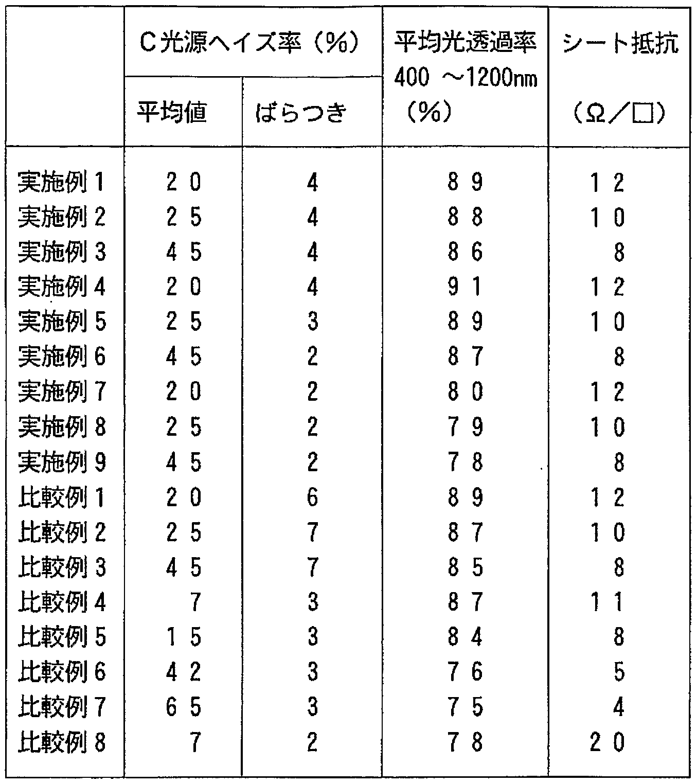
本発明の太陽電池用透明導電性基板は、 C光源ヘイズ率が高く、 基板全体として 見た場合に C光源ヘイズ率のばらつきが少なく、 かつ光透過性、 特に 4 0 0〜1 2 0 0 n mの波長域の光透過率が高いという特徴を有している。 また、 T i〇2 層を 用いているため、 ヘイズ率のばらつきを抑えつつ、 透光性を維持できる。 これによ り、 太陽光を有効に活用でき、 光電変換効率が大幅に改善されるため、 光電変換効 率に優れた太陽電池、 特にシングル構造のアモルファスシリコン系太陽電池に比べ て光電変換効率に優れるタンデム構造の太陽電池に有用である。 The transparent conductive substrate for solar cells of the present invention has a high C light source haze ratio, and when viewed as a whole substrate, there is little variation in the C light source haze ratio, and light transmittance, particularly 400 to 120 nm. The light transmittance in the wavelength region is high. Moreover, the use of the T I_〇 two layers, while suppressing variations in haze ratio can be maintained translucent. As a result, sunlight can be used effectively and the photoelectric conversion efficiency is greatly improved, so that the photoelectric conversion efficiency is higher than that of solar cells with excellent photoelectric conversion efficiency, particularly single-structure amorphous silicon solar cells. It is useful for an excellent tandem solar cell.
Claims
Priority Applications (3)
| Application Number | Priority Date | Filing Date | Title |
|---|---|---|---|
| JP2005506166A JP5068946B2 (en) | 2003-05-13 | 2004-04-28 | Transparent conductive substrate for solar cell and method for producing the same |
| EP04730025A EP1624494A4 (en) | 2003-05-13 | 2004-04-28 | TRANSPARENT CONDUCTIVE SUBSTRATE FOR SOLAR BATTERY AND PROCESS FOR PRODUCING THE SAME |
| US11/271,812 US20060065299A1 (en) | 2003-05-13 | 2005-11-14 | Transparent conductive substrate for solar cells and method for producing the substrate |
Applications Claiming Priority (2)
| Application Number | Priority Date | Filing Date | Title |
|---|---|---|---|
| JP2003-134847 | 2003-05-13 | ||
| JP2003134847 | 2003-05-13 |
Related Child Applications (1)
| Application Number | Title | Priority Date | Filing Date |
|---|---|---|---|
| US11/271,812 Continuation US20060065299A1 (en) | 2003-05-13 | 2005-11-14 | Transparent conductive substrate for solar cells and method for producing the substrate |
Publications (1)
| Publication Number | Publication Date |
|---|---|
| WO2004102677A1 true WO2004102677A1 (en) | 2004-11-25 |
Family
ID=33447160
Family Applications (1)
| Application Number | Title | Priority Date | Filing Date |
|---|---|---|---|
| PCT/JP2004/006130 Ceased WO2004102677A1 (en) | 2003-05-13 | 2004-04-28 | Transparent conductive substrate for solar battery and method for producing same |
Country Status (4)
| Country | Link |
|---|---|
| US (1) | US20060065299A1 (en) |
| EP (1) | EP1624494A4 (en) |
| JP (2) | JP5068946B2 (en) |
| WO (1) | WO2004102677A1 (en) |
Cited By (12)
| Publication number | Priority date | Publication date | Assignee | Title |
|---|---|---|---|---|
| JP2005347490A (en) * | 2004-06-02 | 2005-12-15 | Asahi Glass Co Ltd | Substrate with transparent conductive oxide film, method for producing the same, and photoelectric conversion element |
| WO2006117345A1 (en) * | 2005-04-29 | 2006-11-09 | Agc Flat Glass Europe Sa | Coated substrate and process for the production of a coated substrate |
| JP2007087866A (en) * | 2005-09-26 | 2007-04-05 | Fujikura Ltd | Transparent conductive substrate, method for producing the same, and photoelectric conversion element |
| EP1786047A1 (en) * | 2005-11-11 | 2007-05-16 | Samsung SDI Co., Ltd. | Solar cell and manufacturing method of the same |
| WO2007058118A1 (en) * | 2005-11-17 | 2007-05-24 | Asahi Glass Company, Limited | Transparent conductive substrate for solar cell and process for producing the same |
| JP2008283176A (en) * | 2007-04-13 | 2008-11-20 | Semiconductor Energy Lab Co Ltd | Photoelectric conversion device and manufacturing method thereof |
| WO2011013775A1 (en) | 2009-07-30 | 2011-02-03 | 旭硝子株式会社 | Transparent conductive substrate for solar cells, and solar cell |
| WO2011013719A1 (en) | 2009-07-29 | 2011-02-03 | 旭硝子株式会社 | Transparent conductive substrate for solar cell, and solar cell |
| WO2011108722A1 (en) | 2010-03-05 | 2011-09-09 | Jx日鉱日石エネルギー株式会社 | Transparent conductive substrate for solar cell, method for manufacturing the substrate, and solar cell using the substrate |
| WO2012169602A1 (en) * | 2011-06-08 | 2012-12-13 | 旭硝子株式会社 | Substrate having transparent conductive film attached thereto |
| WO2013047244A1 (en) * | 2011-09-29 | 2013-04-04 | 国立大学法人大阪大学 | Substrate with conductive layer |
| JP2013515373A (en) * | 2009-12-21 | 2013-05-02 | ピーピージー・インダストリーズ・オハイオ・インコーポレイテッド | Silicon thin-film solar cell with improved haze and method for manufacturing the same |
Families Citing this family (60)
| Publication number | Priority date | Publication date | Assignee | Title |
|---|---|---|---|---|
| US6742358B2 (en) * | 2001-06-08 | 2004-06-01 | Elkcorp | Natural gas liquefaction |
| US7871664B2 (en) * | 2006-03-23 | 2011-01-18 | Guardian Industries Corp. | Parabolic trough or dish reflector for use in concentrating solar power apparatus and method of making same |
| JP5222281B2 (en) * | 2006-04-06 | 2013-06-26 | アプライド マテリアルズ インコーポレイテッド | Reactive sputtering of zinc oxide transparent conductive oxide on large area substrates |
| US7674662B2 (en) * | 2006-07-19 | 2010-03-09 | Applied Materials, Inc. | Process for making thin film field effect transistors using zinc oxide |
| US20080105293A1 (en) * | 2006-11-02 | 2008-05-08 | Guardian Industries Corp. | Front electrode for use in photovoltaic device and method of making same |
| US8203073B2 (en) * | 2006-11-02 | 2012-06-19 | Guardian Industries Corp. | Front electrode for use in photovoltaic device and method of making same |
| US20080105298A1 (en) * | 2006-11-02 | 2008-05-08 | Guardian Industries Corp. | Front electrode for use in photovoltaic device and method of making same |
| US8076571B2 (en) * | 2006-11-02 | 2011-12-13 | Guardian Industries Corp. | Front electrode for use in photovoltaic device and method of making same |
| US20080178932A1 (en) * | 2006-11-02 | 2008-07-31 | Guardian Industries Corp. | Front electrode including transparent conductive coating on patterned glass substrate for use in photovoltaic device and method of making same |
| US7964788B2 (en) * | 2006-11-02 | 2011-06-21 | Guardian Industries Corp. | Front electrode for use in photovoltaic device and method of making same |
| US8012317B2 (en) * | 2006-11-02 | 2011-09-06 | Guardian Industries Corp. | Front electrode including transparent conductive coating on patterned glass substrate for use in photovoltaic device and method of making same |
| US20080105299A1 (en) * | 2006-11-02 | 2008-05-08 | Guardian Industries Corp. | Front electrode with thin metal film layer and high work-function buffer layer for use in photovoltaic device and method of making same |
| US20080302414A1 (en) * | 2006-11-02 | 2008-12-11 | Den Boer Willem | Front electrode for use in photovoltaic device and method of making same |
| US8334452B2 (en) | 2007-01-08 | 2012-12-18 | Guardian Industries Corp. | Zinc oxide based front electrode doped with yttrium for use in photovoltaic device or the like |
| US20080169021A1 (en) * | 2007-01-16 | 2008-07-17 | Guardian Industries Corp. | Method of making TCO front electrode for use in photovoltaic device or the like |
| US20080223430A1 (en) * | 2007-03-14 | 2008-09-18 | Guardian Industries Corp. | Buffer layer for front electrode structure in photovoltaic device or the like |
| US20080223436A1 (en) * | 2007-03-15 | 2008-09-18 | Guardian Industries Corp. | Back reflector for use in photovoltaic device |
| WO2008126706A1 (en) | 2007-04-06 | 2008-10-23 | Semiconductor Energy Laboratory Co., Ltd. | Photovoltaic device and method for manufacturing the same |
| US20080254613A1 (en) * | 2007-04-10 | 2008-10-16 | Applied Materials, Inc. | Methods for forming metal interconnect structure for thin film transistor applications |
| US7927713B2 (en) * | 2007-04-27 | 2011-04-19 | Applied Materials, Inc. | Thin film semiconductor material produced through reactive sputtering of zinc target using nitrogen gases |
| US20080308145A1 (en) * | 2007-06-12 | 2008-12-18 | Guardian Industries Corp | Front electrode including transparent conductive coating on etched glass substrate for use in photovoltaic device and method of making same |
| US20080308146A1 (en) * | 2007-06-14 | 2008-12-18 | Guardian Industries Corp. | Front electrode including pyrolytic transparent conductive coating on textured glass substrate for use in photovoltaic device and method of making same |
| US7994508B2 (en) * | 2007-08-02 | 2011-08-09 | Applied Materials, Inc. | Thin film transistors using thin film semiconductor materials |
| CN101842910B (en) * | 2007-11-01 | 2013-03-27 | 株式会社半导体能源研究所 | Method for manufacturing photoelectric conversion device |
| WO2009060808A1 (en) * | 2007-11-09 | 2009-05-14 | Semiconductor Energy Laboratory Co., Ltd. | Photoelectric conversion device and method for manufacturing the same |
| US7888594B2 (en) * | 2007-11-20 | 2011-02-15 | Guardian Industries Corp. | Photovoltaic device including front electrode having titanium oxide inclusive layer with high refractive index |
| US20100275996A1 (en) * | 2007-11-30 | 2010-11-04 | Kaneka Corporation | Silicon-based thin-film photoelectric conversion device |
| US20090194155A1 (en) * | 2008-02-01 | 2009-08-06 | Guardian Industries Corp. | Front electrode having etched surface for use in photovoltaic device and method of making same |
| US20090194157A1 (en) * | 2008-02-01 | 2009-08-06 | Guardian Industries Corp. | Front electrode having etched surface for use in photovoltaic device and method of making same |
| KR101000057B1 (en) * | 2008-02-04 | 2010-12-10 | 엘지전자 주식회사 | Method for manufacturing a solar cell having a multilayer transparent conductive layer |
| US8980066B2 (en) * | 2008-03-14 | 2015-03-17 | Applied Materials, Inc. | Thin film metal oxynitride semiconductors |
| EP2104145A1 (en) * | 2008-03-18 | 2009-09-23 | AGC Flat Glass Europe SA | Glass substrate coated with thin films and method of manufacturing same |
| WO2009117438A2 (en) * | 2008-03-20 | 2009-09-24 | Applied Materials, Inc. | Process to make metal oxide thin film transistor array with etch stopping layer |
| US7879698B2 (en) * | 2008-03-24 | 2011-02-01 | Applied Materials, Inc. | Integrated process system and process sequence for production of thin film transistor arrays using doped or compounded metal oxide semiconductor |
| US8258511B2 (en) | 2008-07-02 | 2012-09-04 | Applied Materials, Inc. | Thin film transistors using multiple active channel layers |
| US8022291B2 (en) * | 2008-10-15 | 2011-09-20 | Guardian Industries Corp. | Method of making front electrode of photovoltaic device having etched surface and corresponding photovoltaic device |
| US20100133094A1 (en) * | 2008-12-02 | 2010-06-03 | Applied Materials, Inc. | Transparent conductive film with high transmittance formed by a reactive sputter deposition |
| US20100163406A1 (en) * | 2008-12-30 | 2010-07-01 | Applied Materials, Inc. | Substrate support in a reactive sputter chamber |
| US20100242953A1 (en) * | 2009-03-27 | 2010-09-30 | Ppg Industries Ohio, Inc. | Solar reflecting mirror having a protective coating and method of making same |
| CN101527325A (en) * | 2009-04-03 | 2009-09-09 | 中国南玻集团股份有限公司 | Transparent conductive substrate for solar cell |
| CN102422428A (en) * | 2009-04-07 | 2012-04-18 | 北美Agc平板玻璃公司 | Improved silicon thin film deposition for photovoltaic device applications |
| JP2010258043A (en) * | 2009-04-21 | 2010-11-11 | Sanyo Electric Co Ltd | Solar cell |
| KR101733718B1 (en) * | 2009-09-24 | 2017-05-10 | 어플라이드 머티어리얼스, 인코포레이티드 | Methods of fabricating metal oxide or metal oxynitride tfts using wet process for source-drain metal etch |
| US8840763B2 (en) * | 2009-09-28 | 2014-09-23 | Applied Materials, Inc. | Methods for stable process in a reactive sputtering process using zinc or doped zinc target |
| JP2011077128A (en) * | 2009-09-29 | 2011-04-14 | Mitsubishi Heavy Ind Ltd | Photoelectric converter |
| DE102009050234A1 (en) | 2009-10-21 | 2011-05-05 | Von Ardenne Anlagentechnik Gmbh | Process for coating a substrate with a TCO layer and thin-film solar cell |
| US9366783B2 (en) * | 2009-12-21 | 2016-06-14 | Ppg Industries Ohio, Inc. | Silicon thin film solar cell having improved underlayer coating |
| US20110146768A1 (en) * | 2009-12-21 | 2011-06-23 | Ppg Industries Ohio, Inc. | Silicon thin film solar cell having improved underlayer coating |
| WO2011087895A2 (en) * | 2010-01-14 | 2011-07-21 | Pilkington Group Limited | Photovoltaic module and method for making the same |
| US8148192B2 (en) * | 2010-02-22 | 2012-04-03 | James P Campbell | Transparent solar cell method of fabrication via float glass process |
| WO2011143404A2 (en) | 2010-05-13 | 2011-11-17 | First Solar, Inc | Photovotaic device conducting layer |
| US8569098B2 (en) * | 2010-06-18 | 2013-10-29 | Semiconductor Energy Laboratory Co., Ltd. | Method for manufacturing photoelectric conversion device |
| US9076909B2 (en) | 2010-06-18 | 2015-07-07 | Semiconductor Energy Laboratory Co., Ltd. | Photoelectric conversion device and method for manufacturing the same |
| CN102403395A (en) * | 2010-09-08 | 2012-04-04 | 亚树科技股份有限公司 | Manufacturing method for controlling haze of conductive substrate |
| JP2013058562A (en) | 2011-09-07 | 2013-03-28 | Semiconductor Energy Lab Co Ltd | Photoelectric conversion device |
| TWI443846B (en) | 2011-11-01 | 2014-07-01 | Ind Tech Res Inst | Transparent conductive layer structure |
| WO2014164194A1 (en) * | 2013-03-12 | 2014-10-09 | Ppg Industries Ohio, Inc. | High haze underlayer for solar cell |
| ES2824428T3 (en) * | 2014-02-11 | 2021-05-12 | Pilkington Group Ltd | Coated glass item and display assembly made from coated glass |
| WO2016075435A1 (en) * | 2014-11-12 | 2016-05-19 | Pilkington Group Limited | Coated glass article, display assembly made therewith and method of making a display assembly |
| WO2016132131A1 (en) | 2015-02-19 | 2016-08-25 | Pilkington Group Limited | A chemical vapour deposition process for depositing an iron doped tin oxide coating and a coated glass article formed thereby |
Citations (11)
| Publication number | Priority date | Publication date | Assignee | Title |
|---|---|---|---|---|
| JPH02168507A (en) * | 1988-09-22 | 1990-06-28 | Asahi Glass Co Ltd | Fluorine doped tin oxide film and method of reducing resistance thereof |
| JPH02503615A (en) * | 1987-05-22 | 1990-10-25 | グラステツク・ソーラー・インコーポレーテツド | Substrate for solar cells |
| JPH06316442A (en) * | 1993-03-12 | 1994-11-15 | Asahi Glass Co Ltd | Multilayer antireflection film having conductivity |
| JPH08151235A (en) * | 1994-09-30 | 1996-06-11 | Nippon Sheet Glass Co Ltd | Glass plate having electrically conductive transparent film and transparent touch panel |
| WO2000063924A1 (en) * | 1999-04-20 | 2000-10-26 | Matsushita Electric Industrial Co., Ltd. | Transparent substrate with conductive multilayer antireflection coating, touch panel using transparent substrate, and electronic device using touch panel |
| JP2001007361A (en) * | 1999-06-17 | 2001-01-12 | Kanegafuchi Chem Ind Co Ltd | Thin-film photoelectric conversion device |
| JP2001036117A (en) * | 1999-05-18 | 2001-02-09 | Nippon Sheet Glass Co Ltd | Photoelectric conversion device board |
| JP2001053307A (en) * | 1999-05-28 | 2001-02-23 | Nippon Sheet Glass Co Ltd | Substrate for photoelectric conversion device, method for manufacturing the same, and photoelectric conversion device using the same |
| JP2001059175A (en) * | 1999-08-18 | 2001-03-06 | Asahi Glass Co Ltd | Tin oxide film, method for producing the same, and apparatus for producing tin oxide film |
| JP2002252361A (en) * | 2000-11-21 | 2002-09-06 | Nippon Sheet Glass Co Ltd | Transparent conductive film, method for manufacturing the same, and photoelectric conversion device provided with the same |
| JP2002260448A (en) * | 2000-11-21 | 2002-09-13 | Nippon Sheet Glass Co Ltd | Conductive film, method for manufacturing the same, substrate including the same, and photoelectric conversion device |
Family Cites Families (10)
| Publication number | Priority date | Publication date | Assignee | Title |
|---|---|---|---|---|
| US3432365A (en) * | 1963-02-07 | 1969-03-11 | North American Rockwell | Composite thermoelectric assembly having preformed intermediate layers of graded composition |
| US5549763A (en) * | 1993-07-26 | 1996-08-27 | Sanyo Electric Co., Ltd. | Photovoltaic device |
| JP2000226234A (en) * | 1998-12-03 | 2000-08-15 | Toto Ltd | Hydrophilic member |
| JP3247876B2 (en) * | 1999-03-09 | 2002-01-21 | 日本板硝子株式会社 | Glass substrate with transparent conductive film |
| US6380480B1 (en) * | 1999-05-18 | 2002-04-30 | Nippon Sheet Glass Co., Ltd | Photoelectric conversion device and substrate for photoelectric conversion device |
| JP4430194B2 (en) * | 1999-05-31 | 2010-03-10 | 日本板硝子株式会社 | Transparent laminate and glass article using the same |
| JP2001114533A (en) * | 1999-10-20 | 2001-04-24 | Nippon Sheet Glass Co Ltd | Glass pane with transparent conductive film and glass article using the same glass pane |
| JP2001177127A (en) * | 1999-12-20 | 2001-06-29 | Nippon Sheet Glass Co Ltd | Board for photoelectric conversion device |
| JP3443641B2 (en) * | 2000-02-10 | 2003-09-08 | 独立行政法人産業技術総合研究所 | Composite oxides with high Seebeck coefficient and high electrical conductivity |
| US6700053B2 (en) * | 2000-07-03 | 2004-03-02 | Komatsu Ltd. | Thermoelectric module |
-
2004
- 2004-04-28 WO PCT/JP2004/006130 patent/WO2004102677A1/en not_active Ceased
- 2004-04-28 JP JP2005506166A patent/JP5068946B2/en not_active Expired - Fee Related
- 2004-04-28 EP EP04730025A patent/EP1624494A4/en not_active Withdrawn
-
2005
- 2005-11-14 US US11/271,812 patent/US20060065299A1/en not_active Abandoned
-
2011
- 2011-06-22 JP JP2011138729A patent/JP5088435B2/en not_active Expired - Fee Related
Patent Citations (11)
| Publication number | Priority date | Publication date | Assignee | Title |
|---|---|---|---|---|
| JPH02503615A (en) * | 1987-05-22 | 1990-10-25 | グラステツク・ソーラー・インコーポレーテツド | Substrate for solar cells |
| JPH02168507A (en) * | 1988-09-22 | 1990-06-28 | Asahi Glass Co Ltd | Fluorine doped tin oxide film and method of reducing resistance thereof |
| JPH06316442A (en) * | 1993-03-12 | 1994-11-15 | Asahi Glass Co Ltd | Multilayer antireflection film having conductivity |
| JPH08151235A (en) * | 1994-09-30 | 1996-06-11 | Nippon Sheet Glass Co Ltd | Glass plate having electrically conductive transparent film and transparent touch panel |
| WO2000063924A1 (en) * | 1999-04-20 | 2000-10-26 | Matsushita Electric Industrial Co., Ltd. | Transparent substrate with conductive multilayer antireflection coating, touch panel using transparent substrate, and electronic device using touch panel |
| JP2001036117A (en) * | 1999-05-18 | 2001-02-09 | Nippon Sheet Glass Co Ltd | Photoelectric conversion device board |
| JP2001053307A (en) * | 1999-05-28 | 2001-02-23 | Nippon Sheet Glass Co Ltd | Substrate for photoelectric conversion device, method for manufacturing the same, and photoelectric conversion device using the same |
| JP2001007361A (en) * | 1999-06-17 | 2001-01-12 | Kanegafuchi Chem Ind Co Ltd | Thin-film photoelectric conversion device |
| JP2001059175A (en) * | 1999-08-18 | 2001-03-06 | Asahi Glass Co Ltd | Tin oxide film, method for producing the same, and apparatus for producing tin oxide film |
| JP2002252361A (en) * | 2000-11-21 | 2002-09-06 | Nippon Sheet Glass Co Ltd | Transparent conductive film, method for manufacturing the same, and photoelectric conversion device provided with the same |
| JP2002260448A (en) * | 2000-11-21 | 2002-09-13 | Nippon Sheet Glass Co Ltd | Conductive film, method for manufacturing the same, substrate including the same, and photoelectric conversion device |
Non-Patent Citations (1)
| Title |
|---|
| See also references of EP1624494A4 * |
Cited By (18)
| Publication number | Priority date | Publication date | Assignee | Title |
|---|---|---|---|---|
| JP2005347490A (en) * | 2004-06-02 | 2005-12-15 | Asahi Glass Co Ltd | Substrate with transparent conductive oxide film, method for producing the same, and photoelectric conversion element |
| RU2430042C2 (en) * | 2005-04-29 | 2011-09-27 | Агк Гласс Юроп | Substrate with coating and method to manufacture substrate with coating |
| WO2006117345A1 (en) * | 2005-04-29 | 2006-11-09 | Agc Flat Glass Europe Sa | Coated substrate and process for the production of a coated substrate |
| JP2008539154A (en) * | 2005-04-29 | 2008-11-13 | エージーシー フラット グラス ユーロップ エスエー | Coated support and method for producing the same |
| AU2006243845B2 (en) * | 2005-04-29 | 2012-05-03 | Agc Glass Europe | Coated substrate and process for the production of a coated substrate |
| US8153265B2 (en) * | 2005-04-29 | 2012-04-10 | Agc Flat Glass Europe | Coated substrate and process for the production of a coated substrate |
| JP2007087866A (en) * | 2005-09-26 | 2007-04-05 | Fujikura Ltd | Transparent conductive substrate, method for producing the same, and photoelectric conversion element |
| EP1786047A1 (en) * | 2005-11-11 | 2007-05-16 | Samsung SDI Co., Ltd. | Solar cell and manufacturing method of the same |
| WO2007058118A1 (en) * | 2005-11-17 | 2007-05-24 | Asahi Glass Company, Limited | Transparent conductive substrate for solar cell and process for producing the same |
| CN100595933C (en) * | 2005-11-17 | 2010-03-24 | 旭硝子株式会社 | Method for producing transparent conductive substrate for solar cell |
| JP2008283176A (en) * | 2007-04-13 | 2008-11-20 | Semiconductor Energy Lab Co Ltd | Photoelectric conversion device and manufacturing method thereof |
| WO2011013719A1 (en) | 2009-07-29 | 2011-02-03 | 旭硝子株式会社 | Transparent conductive substrate for solar cell, and solar cell |
| WO2011013775A1 (en) | 2009-07-30 | 2011-02-03 | 旭硝子株式会社 | Transparent conductive substrate for solar cells, and solar cell |
| JP2013515373A (en) * | 2009-12-21 | 2013-05-02 | ピーピージー・インダストリーズ・オハイオ・インコーポレイテッド | Silicon thin-film solar cell with improved haze and method for manufacturing the same |
| WO2011108722A1 (en) | 2010-03-05 | 2011-09-09 | Jx日鉱日石エネルギー株式会社 | Transparent conductive substrate for solar cell, method for manufacturing the substrate, and solar cell using the substrate |
| KR20130050284A (en) | 2010-03-05 | 2013-05-15 | 고쿠리츠다이가쿠호진 토쿄고교 다이가꾸 | Transparent conductive substrate for solar cell, method for manufacturing the substrate, and solar cell using the substrate |
| WO2012169602A1 (en) * | 2011-06-08 | 2012-12-13 | 旭硝子株式会社 | Substrate having transparent conductive film attached thereto |
| WO2013047244A1 (en) * | 2011-09-29 | 2013-04-04 | 国立大学法人大阪大学 | Substrate with conductive layer |
Also Published As
| Publication number | Publication date |
|---|---|
| EP1624494A4 (en) | 2007-10-10 |
| US20060065299A1 (en) | 2006-03-30 |
| JP5068946B2 (en) | 2012-11-07 |
| JPWO2004102677A1 (en) | 2006-07-13 |
| JP5088435B2 (en) | 2012-12-05 |
| EP1624494A1 (en) | 2006-02-08 |
| JP2011181975A (en) | 2011-09-15 |
Similar Documents
| Publication | Publication Date | Title |
|---|---|---|
| WO2004102677A1 (en) | Transparent conductive substrate for solar battery and method for producing same | |
| CN100595933C (en) | Method for producing transparent conductive substrate for solar cell | |
| US6380480B1 (en) | Photoelectric conversion device and substrate for photoelectric conversion device | |
| US6362414B1 (en) | Transparent layered product and glass article using the same | |
| US6602606B1 (en) | Glass sheet with conductive film, method of manufacturing the same, and photoelectric conversion device using the same | |
| US7846562B2 (en) | Transparent substrate with transparent conductive film, method of manufacturing the same, and photoelectric conversion element including the substrate | |
| EP1061586A2 (en) | Transparent layered product and glass article using the same | |
| JP2002260448A (en) | Conductive film, method for manufacturing the same, substrate including the same, and photoelectric conversion device | |
| EP1230188B1 (en) | Glass sheet with metal oxide film, method of manufacturing the same, and double-glazing unit using the same | |
| US20110132442A1 (en) | Transparent conductive film substrate and solar cell using the substrate | |
| WO2005027229A1 (en) | Base with transparent conductive film and method for producing same | |
| WO2012169602A1 (en) | Substrate having transparent conductive film attached thereto | |
| WO2003017377A1 (en) | Glass plate having electroconductive film formed thereon | |
| JP2017001924A (en) | Glass plate with coating film | |
| JP2001039738A (en) | Glass plate having conductive film, its production and photo-electric transfer device using the glass plate | |
| EP1419997A1 (en) | Low emissivity glass and method for production thereof | |
| JP2003231968A (en) | Substrate, its manufacturing process and photoelectric converter using this substrate | |
| JP2001043741A (en) | Glass plate having conductive film and manufacture thereof, and photoelectric transducer using the same | |
| JP2012084843A (en) | Substrate with transparent conductive oxide film and photoelectric conversion element | |
| WO2012176817A1 (en) | Base having transparent conductive oxide film | |
| JP2002158366A (en) | Photoelectric conversion device | |
| JP2009239301A (en) | Substrate and photoelectric conversion device using the same | |
| JP2012114205A (en) | Transparent conductive membrane substrate and method of manufacturing the same, and solar cell using the substrate | |
| JP2013251377A (en) | Substrate with transparent conductive film for solar cell |
Legal Events
| Date | Code | Title | Description |
|---|---|---|---|
| AK | Designated states |
Kind code of ref document: A1 Designated state(s): AE AG AL AM AT AU AZ BA BB BG BR BW BY BZ CA CH CN CO CR CU CZ DE DK DM DZ EC EE EG ES FI GB GD GE GH GM HR HU ID IL IN IS JP KE KG KP KR KZ LC LK LR LS LT LU LV MA MD MG MK MN MW MX MZ NA NI NO NZ OM PG PH PL PT RO RU SC SD SE SG SK SL SY TJ TM TN TR TT TZ UA UG US UZ VC VN YU ZA ZM ZW |
|
| AL | Designated countries for regional patents |
Kind code of ref document: A1 Designated state(s): BW GH GM KE LS MW MZ NA SD SL SZ TZ UG ZM ZW AM AZ BY KG KZ MD RU TJ TM AT BE BG CH CY CZ DE DK EE ES FI FR GB GR HU IE IT LU MC NL PL PT RO SE SI SK TR BF BJ CF CG CI CM GA GN GQ GW ML MR NE SN TD TG |
|
| 121 | Ep: the epo has been informed by wipo that ep was designated in this application | ||
| WWE | Wipo information: entry into national phase |
Ref document number: 2005506166 Country of ref document: JP |
|
| WWE | Wipo information: entry into national phase |
Ref document number: 2004730025 Country of ref document: EP Ref document number: 11271812 Country of ref document: US |
|
| WWP | Wipo information: published in national office |
Ref document number: 2004730025 Country of ref document: EP |
|
| WWP | Wipo information: published in national office |
Ref document number: 11271812 Country of ref document: US |