USD673923S1 - Arm for wafer transportation for manufacturing semiconductor - Google Patents
Arm for wafer transportation for manufacturing semiconductor Download PDFInfo
- Publication number
- USD673923S1 USD673923S1 US29/396,042 US201129396042F USD673923S US D673923 S1 USD673923 S1 US D673923S1 US 201129396042 F US201129396042 F US 201129396042F US D673923 S USD673923 S US D673923S
- Authority
- US
- United States
- Prior art keywords
- arm
- manufacturing semiconductor
- wafer transportation
- wafer
- transportation
- Prior art date
- Legal status (The legal status is an assumption and is not a legal conclusion. Google has not performed a legal analysis and makes no representation as to the accuracy of the status listed.)
- Active
Links
- 238000004519 manufacturing process Methods 0.000 title claims description 3
- 239000004065 semiconductor Substances 0.000 title claims description 3
Images


Description
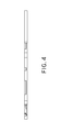
The broken lines in the drawings form no part of the claimed design.
Claims (1)
- The ornamental design for arm for wafer transportation for manufacturing semiconductor, as shown and described.
Applications Claiming Priority (2)
| Application Number | Priority Date | Filing Date | Title |
|---|---|---|---|
| JP2011-001005 | 2011-01-20 | ||
| JP2011001005 | 2011-01-20 |
Publications (1)
| Publication Number | Publication Date |
|---|---|
| USD673923S1 true USD673923S1 (en) | 2013-01-08 |
Family
ID=47428205
Family Applications (1)
| Application Number | Title | Priority Date | Filing Date |
|---|---|---|---|
| US29/396,042 Active USD673923S1 (en) | 2011-01-20 | 2011-06-24 | Arm for wafer transportation for manufacturing semiconductor |
Country Status (2)
| Country | Link |
|---|---|
| US (1) | USD673923S1 (en) |
| TW (1) | TWD147587S (en) |
Cited By (5)
| Publication number | Priority date | Publication date | Assignee | Title |
|---|---|---|---|---|
| USD695240S1 (en) * | 2011-10-20 | 2013-12-10 | Tokyo Electron Limited | Arm for wafer transportation for manufacturing semiconductor |
| USD701498S1 (en) * | 2011-10-20 | 2014-03-25 | Tokyo Electron Limited | Arm for wafer transportation for manufacturing semiconductor |
| USD797709S1 (en) * | 2016-01-20 | 2017-09-19 | World Products, Inc. | Curved folded medical monopole antenna |
| USD993200S1 (en) * | 2020-05-26 | 2023-07-25 | Panasonic Intellectual Property Management Co., Ltd. | Tape feeder |
| USD997892S1 (en) * | 2019-11-28 | 2023-09-05 | Kokusai Electric Corporation | End effector for handling wafers |
Families Citing this family (1)
| Publication number | Priority date | Publication date | Assignee | Title |
|---|---|---|---|---|
| CN112496211A (en) * | 2020-12-09 | 2021-03-16 | 雷雨洁 | Anastomat titanium nail manufacturing equipment with rapid sorting function and manufacturing method |
Citations (16)
| Publication number | Priority date | Publication date | Assignee | Title |
|---|---|---|---|---|
| US5643366A (en) * | 1994-01-31 | 1997-07-01 | Applied Materials, Inc. | Wafer handling within a vacuum chamber using vacuum |
| US6167322A (en) * | 1998-07-10 | 2000-12-26 | Holbrooks; Orville Ray | Intelligent wafer handling system and method |
| US6168669B1 (en) * | 1998-02-24 | 2001-01-02 | Tokyo Electron Limited | Substrate holding apparatus and substrate process system |
| US6183183B1 (en) * | 1997-01-16 | 2001-02-06 | Asm America, Inc. | Dual arm linear hand-off wafer transfer assembly |
| US6216883B1 (en) * | 1998-07-24 | 2001-04-17 | Mitsubishi Denki Kabushiki Kaisha | Wafer holding hand |
| US6293749B1 (en) * | 1997-11-21 | 2001-09-25 | Asm America, Inc. | Substrate transfer system for semiconductor processing equipment |
| US6409453B1 (en) * | 1998-02-18 | 2002-06-25 | Applied Materials, Inc. | End effector for wafer handler in processing system |
| US20030169916A1 (en) * | 2002-02-19 | 2003-09-11 | Toshiba Ceramics Co., Ltd. | Wafer inspection apparatus |
| US20040182417A1 (en) * | 2003-03-17 | 2004-09-23 | Tokyo Electron Limited | Processing system and method for chemically treating a substrate |
| US7186297B2 (en) * | 2000-12-15 | 2007-03-06 | Kabushiki Kaisha Yaskawa Denki | Wafer holding apparatus |
| USD559805S1 (en) * | 2005-08-12 | 2008-01-15 | Tokyo Electron Limited | Stage arm for a semiconductor wafer delivery apparatus |
| US7334826B2 (en) * | 2001-07-13 | 2008-02-26 | Semitool, Inc. | End-effectors for handling microelectronic wafers |
| USD589474S1 (en) * | 2007-06-06 | 2009-03-31 | Tokyo Electron Limited | Wafer holding member |
| US7611182B2 (en) * | 2005-02-25 | 2009-11-03 | Semes Co., Ltd. | Wafer transfer apparatus |
| US7654596B2 (en) * | 2003-06-27 | 2010-02-02 | Mattson Technology, Inc. | Endeffectors for handling semiconductor wafers |
| US20110146578A1 (en) * | 2009-12-17 | 2011-06-23 | Hitachi-Kokusai Electric Inc. | Substrate processing apparatus |
-
2011
- 2011-06-24 US US29/396,042 patent/USD673923S1/en active Active
- 2011-07-07 TW TW100303481F patent/TWD147587S/en unknown
Patent Citations (16)
| Publication number | Priority date | Publication date | Assignee | Title |
|---|---|---|---|---|
| US5643366A (en) * | 1994-01-31 | 1997-07-01 | Applied Materials, Inc. | Wafer handling within a vacuum chamber using vacuum |
| US6183183B1 (en) * | 1997-01-16 | 2001-02-06 | Asm America, Inc. | Dual arm linear hand-off wafer transfer assembly |
| US6293749B1 (en) * | 1997-11-21 | 2001-09-25 | Asm America, Inc. | Substrate transfer system for semiconductor processing equipment |
| US6409453B1 (en) * | 1998-02-18 | 2002-06-25 | Applied Materials, Inc. | End effector for wafer handler in processing system |
| US6168669B1 (en) * | 1998-02-24 | 2001-01-02 | Tokyo Electron Limited | Substrate holding apparatus and substrate process system |
| US6167322A (en) * | 1998-07-10 | 2000-12-26 | Holbrooks; Orville Ray | Intelligent wafer handling system and method |
| US6216883B1 (en) * | 1998-07-24 | 2001-04-17 | Mitsubishi Denki Kabushiki Kaisha | Wafer holding hand |
| US7186297B2 (en) * | 2000-12-15 | 2007-03-06 | Kabushiki Kaisha Yaskawa Denki | Wafer holding apparatus |
| US7334826B2 (en) * | 2001-07-13 | 2008-02-26 | Semitool, Inc. | End-effectors for handling microelectronic wafers |
| US20030169916A1 (en) * | 2002-02-19 | 2003-09-11 | Toshiba Ceramics Co., Ltd. | Wafer inspection apparatus |
| US20040182417A1 (en) * | 2003-03-17 | 2004-09-23 | Tokyo Electron Limited | Processing system and method for chemically treating a substrate |
| US7654596B2 (en) * | 2003-06-27 | 2010-02-02 | Mattson Technology, Inc. | Endeffectors for handling semiconductor wafers |
| US7611182B2 (en) * | 2005-02-25 | 2009-11-03 | Semes Co., Ltd. | Wafer transfer apparatus |
| USD559805S1 (en) * | 2005-08-12 | 2008-01-15 | Tokyo Electron Limited | Stage arm for a semiconductor wafer delivery apparatus |
| USD589474S1 (en) * | 2007-06-06 | 2009-03-31 | Tokyo Electron Limited | Wafer holding member |
| US20110146578A1 (en) * | 2009-12-17 | 2011-06-23 | Hitachi-Kokusai Electric Inc. | Substrate processing apparatus |
Cited By (5)
| Publication number | Priority date | Publication date | Assignee | Title |
|---|---|---|---|---|
| USD695240S1 (en) * | 2011-10-20 | 2013-12-10 | Tokyo Electron Limited | Arm for wafer transportation for manufacturing semiconductor |
| USD701498S1 (en) * | 2011-10-20 | 2014-03-25 | Tokyo Electron Limited | Arm for wafer transportation for manufacturing semiconductor |
| USD797709S1 (en) * | 2016-01-20 | 2017-09-19 | World Products, Inc. | Curved folded medical monopole antenna |
| USD997892S1 (en) * | 2019-11-28 | 2023-09-05 | Kokusai Electric Corporation | End effector for handling wafers |
| USD993200S1 (en) * | 2020-05-26 | 2023-07-25 | Panasonic Intellectual Property Management Co., Ltd. | Tape feeder |
Also Published As
| Publication number | Publication date |
|---|---|
| TWD147587S (en) | 2012-06-11 |
Similar Documents
| Publication | Publication Date | Title |
|---|---|---|
| USD695240S1 (en) | Arm for wafer transportation for manufacturing semiconductor | |
| USD686174S1 (en) | Semiconductor device | |
| USD653633S1 (en) | Semiconductor | |
| USD648290S1 (en) | Semiconductor device | |
| USD717254S1 (en) | Semiconductor device | |
| USD717256S1 (en) | Semiconductor device | |
| USD719113S1 (en) | Semiconductor device | |
| USD679949S1 (en) | Cup | |
| USD742870S1 (en) | Kiosk | |
| USD675369S1 (en) | Reflector | |
| USD647678S1 (en) | Dishrack | |
| USD704557S1 (en) | Bottle | |
| USD694722S1 (en) | Heatsink | |
| USD676976S1 (en) | Analyser | |
| USD660572S1 (en) | Footwear | |
| USD725053S1 (en) | Outer tube for process tube for manufacturing semiconductor wafers | |
| USD710513S1 (en) | Bottle | |
| USD698252S1 (en) | Bottle | |
| USD701498S1 (en) | Arm for wafer transportation for manufacturing semiconductor | |
| USD674365S1 (en) | Arm for wafer transportation for manufacturing semiconductor | |
| USD674495S1 (en) | Pacifier teether | |
| USD720309S1 (en) | Inner tube for process tube for manufacturing semiconductor wafers | |
| USD634930S1 (en) | Case | |
| USD650173S1 (en) | Tool case | |
| USD679281S1 (en) | Support arm |