US7948093B2 - Memory IC package assembly having stair step metal layer and apertures - Google Patents
Memory IC package assembly having stair step metal layer and apertures Download PDFInfo
- Publication number
- US7948093B2 US7948093B2 US11/965,705 US96570507A US7948093B2 US 7948093 B2 US7948093 B2 US 7948093B2 US 96570507 A US96570507 A US 96570507A US 7948093 B2 US7948093 B2 US 7948093B2
- Authority
- US
- United States
- Prior art keywords
- memory
- die
- metal layer
- layer
- package assembly
- Prior art date
- Legal status (The legal status is an assumption and is not a legal conclusion. Google has not performed a legal analysis and makes no representation as to the accuracy of the status listed.)
- Active, expires
Links
Images


Classifications
-
- H—ELECTRICITY
- H01—ELECTRIC ELEMENTS
- H01L—SEMICONDUCTOR DEVICES NOT COVERED BY CLASS H10
- H01L23/00—Details of semiconductor or other solid state devices
- H01L23/48—Arrangements for conducting electric current to or from the solid state body in operation, e.g. leads, terminal arrangements ; Selection of materials therefor
- H01L23/488—Arrangements for conducting electric current to or from the solid state body in operation, e.g. leads, terminal arrangements ; Selection of materials therefor consisting of soldered or bonded constructions
- H01L23/495—Lead-frames or other flat leads
- H01L23/49503—Lead-frames or other flat leads characterised by the die pad
- H01L23/4951—Chip-on-leads or leads-on-chip techniques, i.e. inner lead fingers being used as die pad
-
- H—ELECTRICITY
- H01—ELECTRIC ELEMENTS
- H01L—SEMICONDUCTOR DEVICES NOT COVERED BY CLASS H10
- H01L23/00—Details of semiconductor or other solid state devices
- H01L23/28—Encapsulations, e.g. encapsulating layers, coatings, e.g. for protection
- H01L23/31—Encapsulations, e.g. encapsulating layers, coatings, e.g. for protection characterised by the arrangement or shape
- H01L23/3107—Encapsulations, e.g. encapsulating layers, coatings, e.g. for protection characterised by the arrangement or shape the device being completely enclosed
- H01L23/3114—Encapsulations, e.g. encapsulating layers, coatings, e.g. for protection characterised by the arrangement or shape the device being completely enclosed the device being a chip scale package, e.g. CSP
-
- H—ELECTRICITY
- H01—ELECTRIC ELEMENTS
- H01L—SEMICONDUCTOR DEVICES NOT COVERED BY CLASS H10
- H01L23/00—Details of semiconductor or other solid state devices
- H01L23/48—Arrangements for conducting electric current to or from the solid state body in operation, e.g. leads, terminal arrangements ; Selection of materials therefor
- H01L23/488—Arrangements for conducting electric current to or from the solid state body in operation, e.g. leads, terminal arrangements ; Selection of materials therefor consisting of soldered or bonded constructions
- H01L23/495—Lead-frames or other flat leads
- H01L23/49572—Lead-frames or other flat leads consisting of thin flexible metallic tape with or without a film carrier
-
- H—ELECTRICITY
- H01—ELECTRIC ELEMENTS
- H01L—SEMICONDUCTOR DEVICES NOT COVERED BY CLASS H10
- H01L24/00—Arrangements for connecting or disconnecting semiconductor or solid-state bodies; Methods or apparatus related thereto
- H01L24/01—Means for bonding being attached to, or being formed on, the surface to be connected, e.g. chip-to-package, die-attach, "first-level" interconnects; Manufacturing methods related thereto
- H01L24/42—Wire connectors; Manufacturing methods related thereto
- H01L24/47—Structure, shape, material or disposition of the wire connectors after the connecting process
- H01L24/49—Structure, shape, material or disposition of the wire connectors after the connecting process of a plurality of wire connectors
-
- H—ELECTRICITY
- H01—ELECTRIC ELEMENTS
- H01L—SEMICONDUCTOR DEVICES NOT COVERED BY CLASS H10
- H01L2224/00—Indexing scheme for arrangements for connecting or disconnecting semiconductor or solid-state bodies and methods related thereto as covered by H01L24/00
- H01L2224/01—Means for bonding being attached to, or being formed on, the surface to be connected, e.g. chip-to-package, die-attach, "first-level" interconnects; Manufacturing methods related thereto
- H01L2224/02—Bonding areas; Manufacturing methods related thereto
- H01L2224/04—Structure, shape, material or disposition of the bonding areas prior to the connecting process
- H01L2224/05—Structure, shape, material or disposition of the bonding areas prior to the connecting process of an individual bonding area
- H01L2224/0554—External layer
- H01L2224/05599—Material
-
- H—ELECTRICITY
- H01—ELECTRIC ELEMENTS
- H01L—SEMICONDUCTOR DEVICES NOT COVERED BY CLASS H10
- H01L2224/00—Indexing scheme for arrangements for connecting or disconnecting semiconductor or solid-state bodies and methods related thereto as covered by H01L24/00
- H01L2224/01—Means for bonding being attached to, or being formed on, the surface to be connected, e.g. chip-to-package, die-attach, "first-level" interconnects; Manufacturing methods related thereto
- H01L2224/42—Wire connectors; Manufacturing methods related thereto
- H01L2224/44—Structure, shape, material or disposition of the wire connectors prior to the connecting process
- H01L2224/45—Structure, shape, material or disposition of the wire connectors prior to the connecting process of an individual wire connector
- H01L2224/45001—Core members of the connector
- H01L2224/45099—Material
- H01L2224/451—Material with a principal constituent of the material being a metal or a metalloid, e.g. boron (B), silicon (Si), germanium (Ge), arsenic (As), antimony (Sb), tellurium (Te) and polonium (Po), and alloys thereof
- H01L2224/45138—Material with a principal constituent of the material being a metal or a metalloid, e.g. boron (B), silicon (Si), germanium (Ge), arsenic (As), antimony (Sb), tellurium (Te) and polonium (Po), and alloys thereof the principal constituent melting at a temperature of greater than or equal to 950°C and less than 1550°C
- H01L2224/45139—Silver (Ag) as principal constituent
-
- H—ELECTRICITY
- H01—ELECTRIC ELEMENTS
- H01L—SEMICONDUCTOR DEVICES NOT COVERED BY CLASS H10
- H01L2224/00—Indexing scheme for arrangements for connecting or disconnecting semiconductor or solid-state bodies and methods related thereto as covered by H01L24/00
- H01L2224/01—Means for bonding being attached to, or being formed on, the surface to be connected, e.g. chip-to-package, die-attach, "first-level" interconnects; Manufacturing methods related thereto
- H01L2224/42—Wire connectors; Manufacturing methods related thereto
- H01L2224/44—Structure, shape, material or disposition of the wire connectors prior to the connecting process
- H01L2224/45—Structure, shape, material or disposition of the wire connectors prior to the connecting process of an individual wire connector
- H01L2224/45001—Core members of the connector
- H01L2224/45099—Material
- H01L2224/451—Material with a principal constituent of the material being a metal or a metalloid, e.g. boron (B), silicon (Si), germanium (Ge), arsenic (As), antimony (Sb), tellurium (Te) and polonium (Po), and alloys thereof
- H01L2224/45138—Material with a principal constituent of the material being a metal or a metalloid, e.g. boron (B), silicon (Si), germanium (Ge), arsenic (As), antimony (Sb), tellurium (Te) and polonium (Po), and alloys thereof the principal constituent melting at a temperature of greater than or equal to 950°C and less than 1550°C
- H01L2224/45144—Gold (Au) as principal constituent
-
- H—ELECTRICITY
- H01—ELECTRIC ELEMENTS
- H01L—SEMICONDUCTOR DEVICES NOT COVERED BY CLASS H10
- H01L2224/00—Indexing scheme for arrangements for connecting or disconnecting semiconductor or solid-state bodies and methods related thereto as covered by H01L24/00
- H01L2224/01—Means for bonding being attached to, or being formed on, the surface to be connected, e.g. chip-to-package, die-attach, "first-level" interconnects; Manufacturing methods related thereto
- H01L2224/42—Wire connectors; Manufacturing methods related thereto
- H01L2224/47—Structure, shape, material or disposition of the wire connectors after the connecting process
- H01L2224/48—Structure, shape, material or disposition of the wire connectors after the connecting process of an individual wire connector
- H01L2224/4805—Shape
- H01L2224/4809—Loop shape
- H01L2224/48091—Arched
-
- H—ELECTRICITY
- H01—ELECTRIC ELEMENTS
- H01L—SEMICONDUCTOR DEVICES NOT COVERED BY CLASS H10
- H01L2224/00—Indexing scheme for arrangements for connecting or disconnecting semiconductor or solid-state bodies and methods related thereto as covered by H01L24/00
- H01L2224/01—Means for bonding being attached to, or being formed on, the surface to be connected, e.g. chip-to-package, die-attach, "first-level" interconnects; Manufacturing methods related thereto
- H01L2224/42—Wire connectors; Manufacturing methods related thereto
- H01L2224/47—Structure, shape, material or disposition of the wire connectors after the connecting process
- H01L2224/48—Structure, shape, material or disposition of the wire connectors after the connecting process of an individual wire connector
- H01L2224/481—Disposition
- H01L2224/48151—Connecting between a semiconductor or solid-state body and an item not being a semiconductor or solid-state body, e.g. chip-to-substrate, chip-to-passive
- H01L2224/48221—Connecting between a semiconductor or solid-state body and an item not being a semiconductor or solid-state body, e.g. chip-to-substrate, chip-to-passive the body and the item being stacked
- H01L2224/48225—Connecting between a semiconductor or solid-state body and an item not being a semiconductor or solid-state body, e.g. chip-to-substrate, chip-to-passive the body and the item being stacked the item being non-metallic, e.g. insulating substrate with or without metallisation
- H01L2224/4824—Connecting between the body and an opposite side of the item with respect to the body
-
- H—ELECTRICITY
- H01—ELECTRIC ELEMENTS
- H01L—SEMICONDUCTOR DEVICES NOT COVERED BY CLASS H10
- H01L2224/00—Indexing scheme for arrangements for connecting or disconnecting semiconductor or solid-state bodies and methods related thereto as covered by H01L24/00
- H01L2224/01—Means for bonding being attached to, or being formed on, the surface to be connected, e.g. chip-to-package, die-attach, "first-level" interconnects; Manufacturing methods related thereto
- H01L2224/42—Wire connectors; Manufacturing methods related thereto
- H01L2224/47—Structure, shape, material or disposition of the wire connectors after the connecting process
- H01L2224/48—Structure, shape, material or disposition of the wire connectors after the connecting process of an individual wire connector
- H01L2224/484—Connecting portions
- H01L2224/48463—Connecting portions the connecting portion on the bonding area of the semiconductor or solid-state body being a ball bond
- H01L2224/48465—Connecting portions the connecting portion on the bonding area of the semiconductor or solid-state body being a ball bond the other connecting portion not on the bonding area being a wedge bond, i.e. ball-to-wedge, regular stitch
-
- H—ELECTRICITY
- H01—ELECTRIC ELEMENTS
- H01L—SEMICONDUCTOR DEVICES NOT COVERED BY CLASS H10
- H01L2224/00—Indexing scheme for arrangements for connecting or disconnecting semiconductor or solid-state bodies and methods related thereto as covered by H01L24/00
- H01L2224/01—Means for bonding being attached to, or being formed on, the surface to be connected, e.g. chip-to-package, die-attach, "first-level" interconnects; Manufacturing methods related thereto
- H01L2224/42—Wire connectors; Manufacturing methods related thereto
- H01L2224/47—Structure, shape, material or disposition of the wire connectors after the connecting process
- H01L2224/49—Structure, shape, material or disposition of the wire connectors after the connecting process of a plurality of wire connectors
- H01L2224/491—Disposition
- H01L2224/49105—Connecting at different heights
- H01L2224/49109—Connecting at different heights outside the semiconductor or solid-state body
-
- H—ELECTRICITY
- H01—ELECTRIC ELEMENTS
- H01L—SEMICONDUCTOR DEVICES NOT COVERED BY CLASS H10
- H01L2224/00—Indexing scheme for arrangements for connecting or disconnecting semiconductor or solid-state bodies and methods related thereto as covered by H01L24/00
- H01L2224/73—Means for bonding being of different types provided for in two or more of groups H01L2224/10, H01L2224/18, H01L2224/26, H01L2224/34, H01L2224/42, H01L2224/50, H01L2224/63, H01L2224/71
- H01L2224/732—Location after the connecting process
- H01L2224/73201—Location after the connecting process on the same surface
- H01L2224/73215—Layer and wire connectors
-
- H—ELECTRICITY
- H01—ELECTRIC ELEMENTS
- H01L—SEMICONDUCTOR DEVICES NOT COVERED BY CLASS H10
- H01L2224/00—Indexing scheme for arrangements for connecting or disconnecting semiconductor or solid-state bodies and methods related thereto as covered by H01L24/00
- H01L2224/80—Methods for connecting semiconductor or other solid state bodies using means for bonding being attached to, or being formed on, the surface to be connected
- H01L2224/85—Methods for connecting semiconductor or other solid state bodies using means for bonding being attached to, or being formed on, the surface to be connected using a wire connector
- H01L2224/8538—Bonding interfaces outside the semiconductor or solid-state body
- H01L2224/85399—Material
-
- H—ELECTRICITY
- H01—ELECTRIC ELEMENTS
- H01L—SEMICONDUCTOR DEVICES NOT COVERED BY CLASS H10
- H01L24/00—Arrangements for connecting or disconnecting semiconductor or solid-state bodies; Methods or apparatus related thereto
- H01L24/01—Means for bonding being attached to, or being formed on, the surface to be connected, e.g. chip-to-package, die-attach, "first-level" interconnects; Manufacturing methods related thereto
- H01L24/42—Wire connectors; Manufacturing methods related thereto
- H01L24/44—Structure, shape, material or disposition of the wire connectors prior to the connecting process
- H01L24/45—Structure, shape, material or disposition of the wire connectors prior to the connecting process of an individual wire connector
-
- H—ELECTRICITY
- H01—ELECTRIC ELEMENTS
- H01L—SEMICONDUCTOR DEVICES NOT COVERED BY CLASS H10
- H01L24/00—Arrangements for connecting or disconnecting semiconductor or solid-state bodies; Methods or apparatus related thereto
- H01L24/01—Means for bonding being attached to, or being formed on, the surface to be connected, e.g. chip-to-package, die-attach, "first-level" interconnects; Manufacturing methods related thereto
- H01L24/42—Wire connectors; Manufacturing methods related thereto
- H01L24/47—Structure, shape, material or disposition of the wire connectors after the connecting process
- H01L24/48—Structure, shape, material or disposition of the wire connectors after the connecting process of an individual wire connector
-
- H—ELECTRICITY
- H01—ELECTRIC ELEMENTS
- H01L—SEMICONDUCTOR DEVICES NOT COVERED BY CLASS H10
- H01L2924/00—Indexing scheme for arrangements or methods for connecting or disconnecting semiconductor or solid-state bodies as covered by H01L24/00
- H01L2924/0001—Technical content checked by a classifier
- H01L2924/00014—Technical content checked by a classifier the subject-matter covered by the group, the symbol of which is combined with the symbol of this group, being disclosed without further technical details
-
- H—ELECTRICITY
- H01—ELECTRIC ELEMENTS
- H01L—SEMICONDUCTOR DEVICES NOT COVERED BY CLASS H10
- H01L2924/00—Indexing scheme for arrangements or methods for connecting or disconnecting semiconductor or solid-state bodies as covered by H01L24/00
- H01L2924/01—Chemical elements
- H01L2924/01006—Carbon [C]
-
- H—ELECTRICITY
- H01—ELECTRIC ELEMENTS
- H01L—SEMICONDUCTOR DEVICES NOT COVERED BY CLASS H10
- H01L2924/00—Indexing scheme for arrangements or methods for connecting or disconnecting semiconductor or solid-state bodies as covered by H01L24/00
- H01L2924/01—Chemical elements
- H01L2924/01013—Aluminum [Al]
-
- H—ELECTRICITY
- H01—ELECTRIC ELEMENTS
- H01L—SEMICONDUCTOR DEVICES NOT COVERED BY CLASS H10
- H01L2924/00—Indexing scheme for arrangements or methods for connecting or disconnecting semiconductor or solid-state bodies as covered by H01L24/00
- H01L2924/01—Chemical elements
- H01L2924/01033—Arsenic [As]
-
- H—ELECTRICITY
- H01—ELECTRIC ELEMENTS
- H01L—SEMICONDUCTOR DEVICES NOT COVERED BY CLASS H10
- H01L2924/00—Indexing scheme for arrangements or methods for connecting or disconnecting semiconductor or solid-state bodies as covered by H01L24/00
- H01L2924/01—Chemical elements
- H01L2924/01047—Silver [Ag]
-
- H—ELECTRICITY
- H01—ELECTRIC ELEMENTS
- H01L—SEMICONDUCTOR DEVICES NOT COVERED BY CLASS H10
- H01L2924/00—Indexing scheme for arrangements or methods for connecting or disconnecting semiconductor or solid-state bodies as covered by H01L24/00
- H01L2924/01—Chemical elements
- H01L2924/01079—Gold [Au]
-
- H—ELECTRICITY
- H01—ELECTRIC ELEMENTS
- H01L—SEMICONDUCTOR DEVICES NOT COVERED BY CLASS H10
- H01L2924/00—Indexing scheme for arrangements or methods for connecting or disconnecting semiconductor or solid-state bodies as covered by H01L24/00
- H01L2924/013—Alloys
- H01L2924/014—Solder alloys
-
- H—ELECTRICITY
- H01—ELECTRIC ELEMENTS
- H01L—SEMICONDUCTOR DEVICES NOT COVERED BY CLASS H10
- H01L2924/00—Indexing scheme for arrangements or methods for connecting or disconnecting semiconductor or solid-state bodies as covered by H01L24/00
- H01L2924/10—Details of semiconductor or other solid state devices to be connected
- H01L2924/11—Device type
- H01L2924/14—Integrated circuits
-
- H—ELECTRICITY
- H01—ELECTRIC ELEMENTS
- H01L—SEMICONDUCTOR DEVICES NOT COVERED BY CLASS H10
- H01L2924/00—Indexing scheme for arrangements or methods for connecting or disconnecting semiconductor or solid-state bodies as covered by H01L24/00
- H01L2924/30—Technical effects
- H01L2924/301—Electrical effects
- H01L2924/30107—Inductance
-
- H—ELECTRICITY
- H01—ELECTRIC ELEMENTS
- H01L—SEMICONDUCTOR DEVICES NOT COVERED BY CLASS H10
- H01L2924/00—Indexing scheme for arrangements or methods for connecting or disconnecting semiconductor or solid-state bodies as covered by H01L24/00
- H01L2924/30—Technical effects
- H01L2924/301—Electrical effects
- H01L2924/3011—Impedance
Definitions
- the present invention relates to the field of high speed electronic interconnections for memory and the packaging of semiconductor integrated circuits for use therewith.
- Memory integrated circuits “ICs” for use with most computers operate at speeds slower than current generation central processing unit “CPU” ICs creating a condition generally referred to as the “memory bottleneck”. In such condition, the CPU must remain in a wait state until the memory data is written or retrieved.
- the problem has been addressed, in part, by improved memory system designs.
- electronic systems move into the multi-gigabit per second data rate range, a significant gap remains between top-end operating rates of CPU ICs and memory ICs.
- Part of this ongoing disparity is due to the limits of current interconnection design, which often results, particularly at higher frequencies, in disturbances that contribute to signal distortion. For example, signal distortion can often be due, at least in part to so-called parasitic effects resulting from traditional interconnect designs.
- Parasitic effects and signal discontinuity are primary sources of signal disturbance, thus one of the major objectives in maintaining signal integrity is to eliminate or minimize the parasitic effects and electrical discontinuities impinging upon a signal.
- Parasitic effects and electrical discontinuities are caused by a number of factors such as sharp changes in direction, changes in material, circuit feature flaws and even interconnections, such as solder balls used to connect IC packages to next level interconnection substrates. All these can affect signal integrity by introducing undesirable changes in impedance and creating signal reflections. There is also concern about signal skew, cause by differing signal lengths, which is important in assuring proper signal timing. Finally, cross talk between signals due to inductance is another deleterious effect associated with current packaging structures for memory ICs.
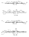
- FIG. 1A shows a cross section of an embodiment of a memory package structure
- FIG. 1B shows exploded view of the main elements of FIG. 1A ;
- FIG. 2A shows a cross section of another embodiment of a memory package structure
- FIG. 2B shows exploded view of the main elements of FIG. 2A ;
- FIG. 3A shows a cross section of another embodiment of a memory package structure
- FIG. 3B shows exploded view of the main elements of FIG. 3A ;
- FIG. 4 shows a cross section of a memory IC package assembly embodiment showing its structure
- FIG. 5 shows a cross section of another memory IC package assembly embodiment showing its structure
- FIG. 6 shows a cross section of another memory IC package assembly embodiment showing its structure
- FIG. 7 shows a perspective view of the elements of construction of an embodiment of a memory IC package assembly
- FIG. 8 shows a perspective view of a partially assembled embodiment of an IC memory package comprised of the elements of FIG. 7 stacked and joined to a memory IC die.
- FIG. 9 shows a top view of a metal layer segmented into a plurality of regions for use as power and ground.
- IC package structures having stair step connections for use with memory devices and which improve control of the quality of an electronic signal that passes though a memory chip package and between memory chips, provide improved thermal management, and lower power consumption than current package designs and structures.
- the embodiments disclosed herein address many of the limitations common to many of the current design and manufacturing practices employed in the fabrication of electronic memory device (e.g. IC or integrated circuit) and system interconnections. Some of those limitations include and inability of current design and manufacturing practices to address fully and adequately the needs for improved electronic signal integrity as the electronic signal transitions between memory chips on an electronic memory module.
- An objective of the present disclosure to describe memory package structures which inexpensively provide direct and uniform controlled impedance across the surface of a memory package by routing high speed signals on a first circuit layer which references directly a metal ground layer proximate to the first circuit layer, wherein the final assembly offers improved signal quality and at lower power consumption.
- Another objective is to describe a memory IC package structure having two metal layers but which does not require or use plated through holes to access the second metal layer (i.e., ground layer).
- FIG. 1A depicts in cross section an embodiment of a memory IC package substrate assembly 100 having apertures 101 which expose directly a metal ground layer to serve as contact point for next level assembly.
- the substrate also has conductor contact points 102 to be used for next level assembly. Other contact points are provided for interconnection to the IC memory die.
- Contact points 103 are for electrical connection to circuit elements and contacts 104 are for electrical connection to the ground layer.
- An insulator would normally cover the non-contact portions of the metal circuits, however the structure is shown without a insulator covering the circuits for brevity.
- FIG. 1B depicts in cross section the elements of the embodiment shown in FIG. 1A where 105 is a dielectric insulation material layer of a suitable material (e.g. polyimide film).
- the dielectric insulation material layer has apertures 106 to allow access to ground layer 109 when sandwiched and has circuits 107 with electrical terminations at both ends for electrical connection as shown in FIG. 1A .
- a suitable adhesive 108 is used to bond the dielectric insulation material 105 with circuits 107 to the ground metal 109 .
- a first aperture 111 extends through the dielectric layer 105 and the adhesive layer 108 .
- a second aperture 112 extends through the ground layer 109 and suitable adhesive 110 to allow access to the bond pads on the memory IC die.
- Aperture 111 is aligned with, but slightly wider than aperture 112 , forming opposing shelves 104 (see FIG. 1A ), the upper surface of the shelves comprising narrow strips of the ground layer 109 that can be accessed through the first aperture 111 .
- the alignment of apertures 111 and 112 is configured to provide access to the bond pads 701 on the memory IC die 700 during assembly of the memory IC package.
- the suitable adhesive 110 serves to bond the assembly to the die and has suitable insulation characteristics.
- one or more of the dielectric insulation layer 105 , the adhesive layer 108 , and the adhesive layer 110 may further function as a stress buffer layers that is particularly suited for ameliorating physical stresses that mechanically impinge on the memory IC package from “next-level” components and connections.
- FIG. 2A depicts in cross section an embodiment of a memory IC package substrate assembly 200 having apertures 201 which expose directly a metal ground layer 207 to serve as contact point for next level assembly.
- the substrate also has conductor contact points 202 to be used for next level assembly.
- Other contact points are provided for interconnection to the IC memory die.
- Contact points 203 are for electrical connection to circuit elements and contacts 204 are for electrical connection to the ground layer.
- An insulator would normally cover the non-contact portions of the metal circuits, however the structure is shown without a insulator covering the circuits for brevity.
- FIG. 2B depicts in cross section the elements of the embodiment shown in FIG. 2A where 206 is a dielectric insulation material layer of a suitable material (e.g. polyimide film).
- the dielectric insulation material layer has apertures 201 to allow access to ground layer 207 which is bonding to one side (e.g. bottom) of the dielectric insulation material 206 .
- Circuits 205 are disposed on the second side (e.g., top surface) of dielectric layer 606 .
- the circuits 205 have electrical terminations at both ends for electrical connection as shown in FIG. 2A .
- a suitable adhesive 208 is used to bond the dielectric insulation material 206 with circuits 205 and ground metal 207 to a memory IC die, such as depicted in FIGS. 4-8 .
- a first aperture 209 extends through the dielectric layer 206 .
- a second aperture 210 extends through the ground layer 207 and through the suitable adhesive 208 .
- Aperture 209 is aligned with, but slightly wider than aperture 210 , thereby forming opposing shelves 204 ( FIG. 2A ), exposing a portion of the ground layer 207 along parallel strips on opposing sides of the aperture.
- the alignment of apertures 209 and 210 is further configured to allow access to the bond pads 701 on the memory IC die 700 during assembly of the memory IC package.
- the suitable adhesive 208 serves to bond the assembly to the die and also, advantageously has suitable insulation characteristics.
- one or more of the dielectric insulation layer 206 , and the adhesive 208 may further function as stress buffer layers that are particularly suited for ameliorating physical stresses that mechanically impinge on the memory IC package from “next-level” components and connections.
- FIG. 3A depicts in cross section an embodiment of a memory IC package substrate assembly 300 having conductive projections 301 which are electrically connected to the ground 307 and which protrude above the surface of the assembly to serve as contact points for the ground for next level assembly.
- the substrate also has circuit conductor contact points 304 to be used for next level assembly.
- Other contact points ( 302 , 303 ) are provided for interconnection to the IC memory die.
- Contact points 303 are for electrical connection between select terminals of the memory die ( FIGS. 4-8 ) and corresponding circuit elements 304 , and between select terminals of the memory die and contacts 302 , for electrical connection to the ground layer.
- An insulator would normally cover the non-contact portions of the conductor circuits, however the structure is shown without a insulator covering the circuits for brevity.
- FIG. 3B depicts in cross section the elements of the embodiment shown in FIG. 3A where 305 is a dielectric insulation material layer of a suitable material (e.g. polyimide film) having circuits 310 provided on one side (e.g., top). The circuits have electrical terminations at both ends for electrical connection as shown in FIG. 3A .
- the dielectric insulation material layer has apertures 309 to allow access to ground layer 307 which is illustrated as having projections (e.g. bumps) disposed to pass through the apertures 309 in dielectric insulation layer 305 .
- a layer comprised of a suitable adhesive 306 has apertures which correspond to those of dielectric insulation layer 305 is disposed between the insulation layer 305 and the ground metal layer 307 .
- a suitable adhesive 308 is used to bond one side (e.g. bottom) of the ground metal 307 surface to a memory IC die.
- a first aperture 311 within the upper layers of FIG. 3B extends through the dielectric layer 305 and the adhesive layer 306 .
- a second aperture 312 extends through the ground layer 307 and through the suitable adhesive layer 308 .
- Aperture 311 is aligned with, but slightly wider than aperture 312 , thereby forming opposing shelves 303 ( FIG. 3A ), exposing a portion of the ground layer 307 along parallel strips on opposing sides of the aperture.
- the alignment of apertures 311 and 312 is further configured to allow access to the select bond pads 701 on the memory IC die 700 during assembly of the memory IC package.
- the suitable adhesive 308 serves to bond the assembly to the die and advantageously includes suitable insulation characteristics.
- the structure shown may be produced by having the ground layer projections pierce the dielectric insulation layer at desired locations in a lamination step in an alternative embodiment.
- one or more of the dielectric insulation layer 305 , the adhesive layer 306 , and the adhesive layer 308 may further function as a stress buffer layers that are particularly suited for ameliorating physical stresses mechanically impinging on the memory IC package from “next-level” components and connections.
- FIG. 4 shows in cross section of a completed IC package assembly embodiment 400 .
- the memory package includes an IC package substrate 401 , such as one of the embodiments illustrated in FIGS. 1-3 in exploded form and FIGS. 4-6 in assembled form.
- the substrate is advantageously comprised of insulation with apertures, circuit layer, ground layer and suitable adhesive.
- the adhesive layer e.g. 110 , 208 , 308
- First wire bond interconnections 403 extend from die terminals to the ground layer.
- Second wire bond connections 404 extend from select terminals of the IC die to corresponding terminals of the circuit layer.
- wire bond interconnections as well as the terminal points to which they are connected, are protected by an encapsulant 407 .
- a first plurality of solder balls 405 make connection to the ground layer and a second plurality of solder balls 406 make connection to circuits.
- an insulating dielectric material is customary and is used to cover exposed circuit areas not used for making connections to the IC die or a next level interconnection assembly (e.g. PCB or electronic module).
- the finished assembly is generically referred to as an area array package and more specifically as a BGA package.
- FIG. 5 shows in cross section another completed IC package assembly embodiment 500 .
- the IC package assembly includes an IC package substrate 401 comprised of insulation with apertures, circuit layer, ground layer and suitable adhesive (i.e., supplying good mechanical joining along with stress buffer capability) such as illustrated in FIGS. 1-3 is bonded to a memory IC die 502 .
- First integral metal bond interconnections 503 form electrical path(s) between select terminals on the die and the ground layer.
- Second integral metal circuit connections 504 form electrical path(s) between select terminals of the IC die and select terminals of the circuit layer.
- a first plurality of solder balls 505 make connection to the ground layer and a second plurality of solder balls 506 make connection to circuits.
- an insulating dielectric material is normally applied to cover expose circuit areas not used for making connections to the IC die or a next level assembly (e.g. PCB or electronic module).
- the finished assembly is generically referred to as an area array package and more specifically as a BGA (ball grid array) package.
- FIG. 6 shows in cross section of a completed IC package assembly embodiment 600 .
- the completed IC package assembly includes an IC package substrate 601 comprised of insulation with apertures, circuit layer, ground layer having conductive projections 605 and suitable adhesive is bonded to a memory IC die 602 .
- First wire bond interconnections 603 form electrical paths between select terminals on the die, and the ground layer.
- Second wire bond connections 604 form electrical paths between select terminals of the IC die and corresponding terminals of the circuit layer. These bond wire connections (not shown), and the terminals to which they are connected, are protected by an encapsulant 607 .
- a first plurality of contacts in the form of metal projections 405 serve to make connection to the ground layer and a second plurality of contacts serve to make connection to circuits.
- an insulating dielectric material would normally be used to cover expose circuit areas not used for making connections to the IC die or a next level assembly (e.g. PCB or electronic module).
- the finished assembly is generically referred to as an area array package and more specifically as a LGA (land grid array) package wherein the contacts are substantially planar.
- FIG. 7 shows in a perspective exploded view the elements of a generalized embodiment the structures shown in FIG. 1 through FIG. 4 and FIG. 6 .
- a memory IC die 700 having central terminals shown as wire bond pads 701 is disposed beneath a suitable adhesive layer 702 which has a central aperture 703 to expose wire bond pads 701 when assembled.
- a ground layer 704 of a suitable metal or other conductive material also has a central aperture 705 to expose the wire bond pads 701 when assembly of package elements to the die is complete.
- a second adhesive layer 706 is disposed above the ground layer 704 and has apertures 708 which serve to expose a plurality of ground contacts when assembled.
- a central aperture 707 is provided in adhesive layer 706 to allow access to the edge of the ground layer during wire bond assembly.
- An area proximate to the edge of the ground metal central aperture may be plated with a wire bondable metal (e.g., gold, silver, etc) to facilitate wire bonding (not shown).
- a wire bondable metal e
- a circuit layer 709 includes dielectric insulation 713 and circuits 712 formed on top of the dielectric insulation 713 .
- Each circuit has a first end that has an interface region 714 for interconnection to a next level interconnection device (e.g. a PCB). Bond pads can be coupled to the interface regions to permit coupling to circuit paths such as wire, integral metal conductors, or other electrically conductive members.
- a second end 715 of each circuit 712 extends to the central aperture 710 to facilitate connection to a wire bond pad 701 of the memory die 700 .
- a central aperture 710 in the dielectric insulation layer 713 is aligned with the aperture 707 adhesive layer 706 , thereby allowing wire bonds to couple the circuits 712 to wire bond pads 701 on the memory IC die.
- a plurality of apertures 711 in the circuit layer 709 are aligned with corresponding apertures in the adhesive layer 708 . As can be better seen in conjunction with FIG. 8 , these apertures 711 expose areas of the ground layer 704 , thereby allowing bond wires or other conductive members to be coupled to the ground layer (directly, or indirectly through the addition of bond pads) through one or more of the apertures 711 .
- FIG. 8 shows in a perspective view of the elements shown in FIG. 7 in the form of a memory IC die package assembly 800 .
- a memory IC die 700 has central terminals shown as wire bond pads 701 exposed through an alignment of apertures 703 , 705 , 707 and 710 described in FIG. 7 , collectively forming central aperture 802 ( FIG. 8 ).
- the aperture 710 of the circuit layer 709 is wider than the aperture 705 in the ground layer, thereby forming parallel shelves 804 A and 804 B, exposing a portion of the ground layer 704 in a stair step relationship to the conductive layer 709 .
- Each of the shelves 804 A, 804 B is large enough to attach bond pads for electrical wire bond connections, and the central aperture 804 is large enough to allow bond wires to be coupled to the bond pads 701 on the memory IC die 700 .
- FIG. 9 shows an alternative embodiment of the metal layer where the metal layer is segmented to provide a plurality of ground and power features.
- the ground layer circuit could be desirably produced directly on a wafer of memory (or other) circuits above an interposed layer of dielectric material having stress buffering capability and one or more stepped layers of metal circuits bonded to the top thereof providing both connection and additional stress buffering capability by means of a suitable adhesive.
- apertures disclosed can be created either before assembly using punching and drilling methods prior to lamination or after circuit package assembly using laser technology to ablate the apertures.
- circuits could be built up by means of alternating layers of polymer and deposited metals to create finished structures which will be within the scope of this disclosure.
- many specific details have been included herein which are not essential to make and use every embodiment of the invention. These details have been included to assist the reader in more easily understanding and comprehending the embodiments described herein. Accordingly, the specification and drawings of this disclosure should be regarded in an illustrative rather than a restrictive sense.
Landscapes
- Engineering & Computer Science (AREA)
- Microelectronics & Electronic Packaging (AREA)
- Computer Hardware Design (AREA)
- Power Engineering (AREA)
- Physics & Mathematics (AREA)
- Condensed Matter Physics & Semiconductors (AREA)
- General Physics & Mathematics (AREA)
- Semiconductor Memories (AREA)
Abstract
Description
Claims (20)
Priority Applications (1)
| Application Number | Priority Date | Filing Date | Title |
|---|---|---|---|
| US11/965,705 US7948093B2 (en) | 2006-12-28 | 2007-12-27 | Memory IC package assembly having stair step metal layer and apertures |
Applications Claiming Priority (3)
| Application Number | Priority Date | Filing Date | Title |
|---|---|---|---|
| US87769106P | 2006-12-28 | 2006-12-28 | |
| US92084507P | 2007-03-30 | 2007-03-30 | |
| US11/965,705 US7948093B2 (en) | 2006-12-28 | 2007-12-27 | Memory IC package assembly having stair step metal layer and apertures |
Publications (2)
| Publication Number | Publication Date |
|---|---|
| US20080211071A1 US20080211071A1 (en) | 2008-09-04 |
| US7948093B2 true US7948093B2 (en) | 2011-05-24 |
Family
ID=39732481
Family Applications (1)
| Application Number | Title | Priority Date | Filing Date |
|---|---|---|---|
| US11/965,705 Active 2029-09-10 US7948093B2 (en) | 2006-12-28 | 2007-12-27 | Memory IC package assembly having stair step metal layer and apertures |
Country Status (1)
| Country | Link |
|---|---|
| US (1) | US7948093B2 (en) |
Cited By (2)
| Publication number | Priority date | Publication date | Assignee | Title |
|---|---|---|---|---|
| US20090091019A1 (en) * | 2003-11-17 | 2009-04-09 | Joseph Charles Fjelstad | Memory Packages Having Stair Step Interconnection Layers |
| US10026666B2 (en) | 2013-10-18 | 2018-07-17 | Rambus Inc. | Stacked die package with aligned active and passive through-silicon vias |
Families Citing this family (1)
| Publication number | Priority date | Publication date | Assignee | Title |
|---|---|---|---|---|
| US11848261B2 (en) * | 2020-10-08 | 2023-12-19 | Ciena Corporation | Low RF crosstalk devices via a slot for isolation |
Citations (13)
| Publication number | Priority date | Publication date | Assignee | Title |
|---|---|---|---|---|
| US5583378A (en) * | 1994-05-16 | 1996-12-10 | Amkor Electronics, Inc. | Ball grid array integrated circuit package with thermal conductor |
| US5844168A (en) * | 1995-08-01 | 1998-12-01 | Minnesota Mining And Manufacturing Company | Multi-layer interconnect sutructure for ball grid arrays |
| US6218731B1 (en) * | 1999-05-21 | 2001-04-17 | Siliconware Precision Industries Co., Ltd. | Tiny ball grid array package |
| US20010002321A1 (en) * | 1999-11-15 | 2001-05-31 | Castro Abram M. | Ball grid substrate for lead-on-chip semiconductor package |
| US6373131B1 (en) * | 1997-05-07 | 2002-04-16 | Signetics | TBGA semiconductor package |
| US6396141B2 (en) * | 1998-10-14 | 2002-05-28 | 3M Innovative Properties Company | Tape ball grid array with interconnected ground plane |
| US20020109226A1 (en) * | 2001-02-15 | 2002-08-15 | Broadcom Corporation | Enhanced die-down ball grid array and method for making the same |
| US6489667B1 (en) * | 1998-10-31 | 2002-12-03 | Amkor Technology, Inc. | Semiconductor device and method of manufacturing such device |
| US20030222344A1 (en) * | 2002-05-30 | 2003-12-04 | Fujitsu Limited | Semiconductor device having a heat spreader exposed from a seal resin |
| US20030230799A1 (en) * | 2002-06-17 | 2003-12-18 | Micron Technology, Inc. | Intrinsic thermal enhancement for FBGA package |
| US20040004277A1 (en) * | 2002-07-03 | 2004-01-08 | Chung-Che Tsai | Semiconductor package with reinforced substrate and fabrication method of the substrate |
| US20050104209A1 (en) * | 2003-11-18 | 2005-05-19 | Sun-Won Kang | Semiconductor chip package having decoupling capacitor and manufacturing method thereof |
| US7592709B2 (en) * | 2005-10-27 | 2009-09-22 | Samsung Electronics Co., Ltd. | Board on chip package and method of manufacturing the same |
-
2007
- 2007-12-27 US US11/965,705 patent/US7948093B2/en active Active
Patent Citations (13)
| Publication number | Priority date | Publication date | Assignee | Title |
|---|---|---|---|---|
| US5583378A (en) * | 1994-05-16 | 1996-12-10 | Amkor Electronics, Inc. | Ball grid array integrated circuit package with thermal conductor |
| US5844168A (en) * | 1995-08-01 | 1998-12-01 | Minnesota Mining And Manufacturing Company | Multi-layer interconnect sutructure for ball grid arrays |
| US6373131B1 (en) * | 1997-05-07 | 2002-04-16 | Signetics | TBGA semiconductor package |
| US6396141B2 (en) * | 1998-10-14 | 2002-05-28 | 3M Innovative Properties Company | Tape ball grid array with interconnected ground plane |
| US6489667B1 (en) * | 1998-10-31 | 2002-12-03 | Amkor Technology, Inc. | Semiconductor device and method of manufacturing such device |
| US6218731B1 (en) * | 1999-05-21 | 2001-04-17 | Siliconware Precision Industries Co., Ltd. | Tiny ball grid array package |
| US20010002321A1 (en) * | 1999-11-15 | 2001-05-31 | Castro Abram M. | Ball grid substrate for lead-on-chip semiconductor package |
| US20020109226A1 (en) * | 2001-02-15 | 2002-08-15 | Broadcom Corporation | Enhanced die-down ball grid array and method for making the same |
| US20030222344A1 (en) * | 2002-05-30 | 2003-12-04 | Fujitsu Limited | Semiconductor device having a heat spreader exposed from a seal resin |
| US20030230799A1 (en) * | 2002-06-17 | 2003-12-18 | Micron Technology, Inc. | Intrinsic thermal enhancement for FBGA package |
| US20040004277A1 (en) * | 2002-07-03 | 2004-01-08 | Chung-Che Tsai | Semiconductor package with reinforced substrate and fabrication method of the substrate |
| US20050104209A1 (en) * | 2003-11-18 | 2005-05-19 | Sun-Won Kang | Semiconductor chip package having decoupling capacitor and manufacturing method thereof |
| US7592709B2 (en) * | 2005-10-27 | 2009-09-22 | Samsung Electronics Co., Ltd. | Board on chip package and method of manufacturing the same |
Cited By (2)
| Publication number | Priority date | Publication date | Assignee | Title |
|---|---|---|---|---|
| US20090091019A1 (en) * | 2003-11-17 | 2009-04-09 | Joseph Charles Fjelstad | Memory Packages Having Stair Step Interconnection Layers |
| US10026666B2 (en) | 2013-10-18 | 2018-07-17 | Rambus Inc. | Stacked die package with aligned active and passive through-silicon vias |
Also Published As
| Publication number | Publication date |
|---|---|
| US20080211071A1 (en) | 2008-09-04 |
Similar Documents
| Publication | Publication Date | Title |
|---|---|---|
| US9461015B2 (en) | Enhanced stacked microelectronic assemblies with central contacts | |
| US7719116B2 (en) | Semiconductor device having reduced number of external pad portions | |
| US6400010B1 (en) | Substrate including a metal portion and a resin portion | |
| US8633587B2 (en) | Package structure | |
| US8786083B2 (en) | Impedance controlled packages with metal sheet or 2-layer RDL | |
| KR100935854B1 (en) | Microelectronic assembly with impedance controlled wirebond and reference wirebond | |
| KR100508682B1 (en) | Stack chip package of heat emission type using dummy wire | |
| US7611981B1 (en) | Optimized circuit design layout for high performance ball grid array packages | |
| US7466021B2 (en) | Memory packages having stair step interconnection layers | |
| US7388279B2 (en) | Tapered dielectric and conductor structures and applications thereof | |
| US9136197B2 (en) | Impedence controlled packages with metal sheet or 2-layer RDL | |
| US20050093152A1 (en) | Multi-surface contact IC packaging structures and assemblies | |
| US7948093B2 (en) | Memory IC package assembly having stair step metal layer and apertures | |
| US6563208B2 (en) | Semiconductor package with conductor impedance selected during assembly | |
| US6566761B1 (en) | Electronic device package with high speed signal interconnect between die pad and external substrate pad | |
| US20040245651A1 (en) | Semiconductor device and method for fabricating the same | |
| KR100702970B1 (en) | Semiconductor package having binary connection method and manufacturing method thereof | |
| US5977617A (en) | Semiconductor device having multilayer film carrier | |
| JPH04290258A (en) | Multichip module | |
| US6545350B2 (en) | Integrated circuit packages and the method for the same | |
| JP2012248877A (en) | Semiconductor package having low speed and high speed signal paths | |
| JP2005101186A (en) | Multilayer semiconductor integrated circuit | |
| JP2002270723A (en) | Semiconductor device, semiconductor chip, and mounting board | |
| KR100471415B1 (en) | Tbga semiconductor package | |
| KR100381844B1 (en) | Circuit Tape for Semiconductor Package |
Legal Events
| Date | Code | Title | Description |
|---|---|---|---|
| AS | Assignment |
Owner name: SILICON PIPE, CALIFORNIA Free format text: ASSIGNMENT OF ASSIGNORS INTEREST;ASSIGNOR:FJELSTAD, JOSEPH CHARLES;REEL/FRAME:021315/0350 Effective date: 20020523 |
|
| AS | Assignment |
Owner name: SECURE NOTE HOLDERS: DAN ANDERSON, JOSEPH FJELSTAD Free format text: ASSIGNMENT OF ASSIGNORS INTEREST;ASSIGNOR:SILICON PIPE, INC.;REEL/FRAME:021380/0249 Effective date: 20080107 |
|
| AS | Assignment |
Owner name: NOVIAS, LLC, CALIFORNIA Free format text: ASSIGNMENT OF ASSIGNORS INTEREST;ASSIGNORS:ANDERSON, DAN;FJELSTAD, JOE;GRUNDY, KEVIN;AND OTHERS;REEL/FRAME:021731/0712 Effective date: 20080301 |
|
| AS | Assignment |
Owner name: INTERCONNECT PORTFOLIO, LLC, CALIFORNIA Free format text: ASSIGNMENT OF ASSIGNORS INTEREST;ASSIGNOR:NOVIAS, LLC;REEL/FRAME:021861/0111 Effective date: 20080314 |
|
| AS | Assignment |
Owner name: TECHNOLOGY PROPERTIES LIMITED LLC, CALIFORNIA Free format text: LICENSE;ASSIGNOR:INTERCONNECT PORTFOLIO LLC;REEL/FRAME:022343/0351 Effective date: 20080315 Owner name: TECHNOLOGY PROPERTIES LIMITED LLC,CALIFORNIA Free format text: LICENSE;ASSIGNOR:INTERCONNECT PORTFOLIO LLC;REEL/FRAME:022343/0351 Effective date: 20080315 |
|
| AS | Assignment |
Owner name: SAMSUNG ELECTRONICS CO., LTD., KOREA, REPUBLIC OF Free format text: ASSIGNMENT OF ASSIGNORS INTEREST;ASSIGNORS:INTERCONNECT PORTFOLIO, LLC;INTELLASYS BEC LIMITED;TECHNOLOGY PROPERTIES LIMITED;REEL/FRAME:025105/0634 Effective date: 20100914 Owner name: SAMSUNG ELECTRONICS CO., LTD., KOREA, REPUBLIC OF Free format text: ASSIGNMENT OF ASSIGNORS INTEREST;ASSIGNOR:TECHNOLOGY PROPERTIES LIMITED;REEL/FRAME:025105/0596 Effective date: 20100610 |
|
| STCF | Information on status: patent grant |
Free format text: PATENTED CASE |
|
| FEPP | Fee payment procedure |
Free format text: PAT HOLDER NO LONGER CLAIMS SMALL ENTITY STATUS, ENTITY STATUS SET TO UNDISCOUNTED (ORIGINAL EVENT CODE: STOL); ENTITY STATUS OF PATENT OWNER: LARGE ENTITY |
|
| FPAY | Fee payment |
Year of fee payment: 4 |
|
| MAFP | Maintenance fee payment |
Free format text: PAYMENT OF MAINTENANCE FEE, 8TH YEAR, LARGE ENTITY (ORIGINAL EVENT CODE: M1552); ENTITY STATUS OF PATENT OWNER: LARGE ENTITY Year of fee payment: 8 |
|
| MAFP | Maintenance fee payment |
Free format text: PAYMENT OF MAINTENANCE FEE, 12TH YEAR, LARGE ENTITY (ORIGINAL EVENT CODE: M1553); ENTITY STATUS OF PATENT OWNER: LARGE ENTITY Year of fee payment: 12 |