US7393758B2 - Wafer level packaging process - Google Patents
Wafer level packaging process Download PDFInfo
- Publication number
- US7393758B2 US7393758B2 US11/265,810 US26581005A US7393758B2 US 7393758 B2 US7393758 B2 US 7393758B2 US 26581005 A US26581005 A US 26581005A US 7393758 B2 US7393758 B2 US 7393758B2
- Authority
- US
- United States
- Prior art keywords
- wafer
- substrate
- devices
- vias
- bonding
- Prior art date
- Legal status (The legal status is an assumption and is not a legal conclusion. Google has not performed a legal analysis and makes no representation as to the accuracy of the status listed.)
- Active, expires
Links
Images


Classifications
-
- B—PERFORMING OPERATIONS; TRANSPORTING
- B81—MICROSTRUCTURAL TECHNOLOGY
- B81C—PROCESSES OR APPARATUS SPECIALLY ADAPTED FOR THE MANUFACTURE OR TREATMENT OF MICROSTRUCTURAL DEVICES OR SYSTEMS
- B81C1/00—Manufacture or treatment of devices or systems in or on a substrate
- B81C1/00015—Manufacture or treatment of devices or systems in or on a substrate for manufacturing microsystems
- B81C1/00261—Processes for packaging MEMS devices
- B81C1/00301—Connecting electric signal lines from the MEMS device with external electrical signal lines, e.g. through vias
-
- H—ELECTRICITY
- H01—ELECTRIC ELEMENTS
- H01L—SEMICONDUCTOR DEVICES NOT COVERED BY CLASS H10
- H01L21/00—Processes or apparatus adapted for the manufacture or treatment of semiconductor or solid state devices or of parts thereof
- H01L21/70—Manufacture or treatment of devices consisting of a plurality of solid state components formed in or on a common substrate or of parts thereof; Manufacture of integrated circuit devices or of parts thereof
- H01L21/71—Manufacture of specific parts of devices defined in group H01L21/70
- H01L21/768—Applying interconnections to be used for carrying current between separate components within a device comprising conductors and dielectrics
- H01L21/76898—Applying interconnections to be used for carrying current between separate components within a device comprising conductors and dielectrics formed through a semiconductor substrate
-
- B—PERFORMING OPERATIONS; TRANSPORTING
- B81—MICROSTRUCTURAL TECHNOLOGY
- B81B—MICROSTRUCTURAL DEVICES OR SYSTEMS, e.g. MICROMECHANICAL DEVICES
- B81B2207/00—Microstructural systems or auxiliary parts thereof
- B81B2207/09—Packages
- B81B2207/091—Arrangements for connecting external electrical signals to mechanical structures inside the package
- B81B2207/094—Feed-through, via
- B81B2207/096—Feed-through, via through the substrate
-
- H—ELECTRICITY
- H01—ELECTRIC ELEMENTS
- H01L—SEMICONDUCTOR DEVICES NOT COVERED BY CLASS H10
- H01L2224/00—Indexing scheme for arrangements for connecting or disconnecting semiconductor or solid-state bodies and methods related thereto as covered by H01L24/00
- H01L2224/01—Means for bonding being attached to, or being formed on, the surface to be connected, e.g. chip-to-package, die-attach, "first-level" interconnects; Manufacturing methods related thereto
- H01L2224/10—Bump connectors; Manufacturing methods related thereto
- H01L2224/11—Manufacturing methods
Definitions
- the present invention relates to the field of wafer level packaging.
- MEMS micro-electro-mechanical system
- a common way of providing electrical lead-outs is through lateral feed-through lines to the edge of the die, which is then sealed by a cap wafer bonded over the die.
- the feed-through lines crossing the bond rim usually don't allow a metal-related bond. Instead, a dielectric-bond is necessary in this arrangement.
- this lateral lead-out has relatively long feed-through lines, which leads to large parasitic capacitances, cross-talk and substantial interconnection resistances. This technique also precludes any wafer level bumping process.
- wafer-level-packages with vertical feed-throughs have been disclosed. Via forming, metal(s) filling and both side metallization are done on a separate single dielectric wafer, such as glass or ceramic. This wafer bonded to a MEMS wafer completes the wafer process, or alternatively, this wafer is just a base material on top of which MEMS devices are built.
- U.S. Pat. No. 6,384,353 also discloses a method of building a MEMS device on a substrate with filled vias and metallization on both sides, though little processing is described.
- a wafer with vias calls for substrate rigidity (i.e., wafer thickness) that increases the difficulty/cost of the via process, and also leads to high parasitic coupling capacitances.
- through holes as vertical feed-through paths are firstly formed in a glass wafer. Then the glass wafer is bonded to a MEMS silicon wafer by anodic bonding to form a hermetic package, while the metal pads on the silicon substrate are aligned to the glass vias and thus exposed. The exposed pads allow a further metallization process on the outer surface of the glass wafer to complete the interconnection.
- Another approach is to fill up the glass vias with metal(s) electro-plated studs and metallization on the glass surface, followed by the anodic bonding to the MEMS wafer to complete the whole process.
- U.S. Pat. No. 6,528,344 discloses another way of forming vertical feed-throughs by use of a cap of silicon. Deep trenches are etched on the silicon cap wafer (only those silicon areas for feed-throughs are not etched), filled with dielectric material, and formed recess of dielectric material for cap gap. After bonding this wafer and the MEMS wafer, contact pads/electrodes of MEMS devices are connected to the silicon islands. Then the cap silicon side of the bonded stack is thinned down to reach or exceed the dielectric materials from the bottom side, so that the silicon islands are exposed and ready for further process to make interconnection.
- This approach uses silicon as part of the feed-through material and thus a relatively large series resistance is expected.
- vias are solidly filled with metal(s) as feed-through paths. This might cause thermal stress issue due to the large thermal mismatch between substrate and metal(s) and hence device reliability issue.
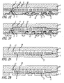
- FIGS. 1 a through 1 f illustrate one embodiment of the present invention.
- FIGS. 2 a through 2 e illustrate another embodiment of the present invention.
- FIGS. 3 a through 3 h illustrate still another embodiment of the present invention.
- FIGS. 3 i through 3 k illustrate variations of the present invention.
- FIGS. 4 a , 4 b , 5 a and 5 b illustrate some details of the processing for opening the bottom of the metal pads inside the vias.
- FIG. 6 illustrates a further embodiment of the present invention.
- An objective of this invention is to assemble MEMS or electronic devices/integrated circuits (ICs) in a wafer-level package format.
- the package can be optionally hermetically sealed by use of bonding techniques like anodic bonding, thermal compression bonding, glass frit bonding or eutectic bonding. All the interconnections are led out through vertical vias on one side of the bonded wafer stack in order to shorten the path of the feed-through; hence the feed-through resistance is minimized. Electric isolation between feed-throughs is formed on bulk material like glass or dielectric-coated-silicon, and thus the capacitive coupling can also be minimized. As a result, minimized feed-through resistance and coupling capacitance can be obtained at the same time.
- Another objective of this invention is to package the devices/structures with a controllable cap gap between one of the device/structure surfaces and the cap electrode. This is important for MEMS structures since additional control flexibility is introduced which will result in improved performance and reliability.
- a controlled cap gap may be used to provide motion limits (mechanical stops) and/or electrostatic drivers for imparting motion to a MEMS device.
- Still another objective of this invention is to form a mechanical structure with minimized thermal-stresses due to thermal expansion mismatch between substrate and the filled metal(s)/alloy.
- metals usually have much higher thermal expansion than silicon or glass, vias filled with solid metal plug/stud may encounter very high thermal stress problems or even changing surface height/roughness on top of the via, which will cause a variable top surface and thus non-stable performance.
- FIGS. 1 a through 1 f A first embodiment of the invented wafer level package fabrication process is illustrated in FIGS. 1 a through 1 f .
- the DEVICE 1 to be packaged may be a MEMS device, an integrated circuit or some other device, hereafter simply a DEVICE, normally of silicon, mounted on a substrate 2 (e.g., in this embodiment, glass), as shown in FIG. 1 a .
- the electrically conductive regions to lead outs 5 can be, by way of example, doped silicon, metal, an alloy layer or stack on substrate 2 or DEVICE 1 or both, or a combination of such materials.
- the outer surface of DEVICE 1 can be bonded with another glass cap wafer 6 .
- the bonding surface can be formed by either a fine polishing after thinning (e.g., grinding, milling or etching) of the DEVICE layer 1 , or an etch stop layer buried in the original DEVICE substrate, or a fine control of the DEVICE layer thinning process, or just planar processes on substrate 2 .
- Isolated conductive island 3 is formed by a DEVICE layer etch process where through trenches 4 on DEVICE layer are formed.
- Another starting material is a cap wafer with cavity 8 and optional conductive layer 9 on it.
- Optional DEVICE structures/layers can also be attached to the recessed side of the cap wafer 6 (not shown in the Figures).
- Optional dielectric bumps (or non-conductive regions) 10 can be deposited on top of the conductive layer 9 to prevent stiction during processing or operation of a MEMS device.
- the conductive layer 9 in the cavity 8 of this embodiment has an extension region 7 that is outside the cavity (or an un-recessed region in the cavity). As shall subsequently be seen, the extension region 7 provides a means of leading the cap electrode out in the wafer level package.
- the first step is to bond the two starting materials, DEVICE 1 on substrate 2 , and cap 6 , together by anodic bonding or other hermetic bonding such as thermal compression bonding (metal-metal bonding, which needs both side metal-coated and patterned) or eutectic bonding (one surface metal-coated and patterned).
- Anodic bonding is highly preferred as a reliable, high quality and reproducible technique.
- the gap between the capping wafer 6 and DEVICE 1 can be well defined ( FIG. 1 b ) using conventional techniques.
- the substrate 2 is thinned down to a preferred thickness by etching, milling or grinding and polishing the surface.
- via 11 is formed either by patterning and etching a masking layer followed by a via wet etching, dry etching, drilling, ultrasonic milling, laser drilling, sand blasting, water jetting, deep etch, or by other mechanical/laser drilling means, or by a combined method.
- Via etch can be stopped simultaneously on conductive DEVICE layer 3 and the conductive layer 5 on substrate 2 .
- the masking layer is removed, and the vias can be optionally fine-tuned by an additional etch to ensure good yield ( FIG. 1 c ).
- the next step is to make electrical interconnections by leading the conductive regions 5 electrically connected to the DEVICE structure to an outer surface of the bonded stack.
- At least two options can be used here.
- the first option is to plate metal(s) 12 through patterned photo-resist on top of a seed conductive layer, then to strip the photo-resist and seed layer after plating.
- the second option is to deposit, pattern and etch the conductive metal layer(s) 12 .
- the major wafer level package process is completed ( FIG. 1 d ) and the device can be packaged as normal integrated circuit (IC) chips after dicing the wafer.
- IC integrated circuit
- the wafer can be further processed after this step for flip-chip assembly or as a surface mountable device (SMD).
- SMD surface mountable device
- Solder bumping on wafer is one of the ways to achieve this.
- a dielectric passivation layer 13 is coated on substrate 2 and patterned to form contact openings 14 on top of the conductive metal(s) 12 ( FIG. 1 e ).
- solder joints can be formed by either plating through a patterned photo-resist or screen printing through a stencil mask. A final stripping of seed layers and (or) photo-resist followed by a solder re-flow will complete the whole process ( FIG. 1 f ).
- the substrate wafer 2 only, with conductive regions 5 on one of its surfaces (without the extra stacked height of DEVICE 1 on top) can be bonded with a cap wafer 6 (as shown in FIG. 6 ), followed by the same process as described above.
- the optional cap electrode 9 is led out to part of the bond areas 7 and a via formed there provides a feed-through of cap electrode 9 to the final interconnection surface.
- a second embodiment of this invention is schematically shown in FIGS. 2 a through 2 e .
- the major difference between the second embodiment and the first embodiment is the cavity depth in the cap wafer 26 .
- cap wafer 26 needs to bond to substrate 2 in the field areas below the top-most surface of DEVICE layer 1 on the substrate wafer 2 , some variations have to be made.
- the field areas (including the surrounding areas for bond) on DEVICE structure 1 on substrate 2 must be bondable.
- Another adjustment on the DEVICE layer 1 is that there is no isolated conductive DEVICE layer island 3 for cap electrode interconnection. Instead, a bulk cap region 23 for the same purpose can easily implement this.
- a conductive layer like conductive layer 9 on the cap wafer 6 of the prior embodiment is not necessary if the cap wafer 26 is conductive, like silicon.
- the starting materials are DEVICE layer 1 on substrate wafer 2 and the cap wafer 26 .
- Cap wafer 26 has recessed cavity 27 and optional dielectric bump region 28 on the bottom of the cavity 27 .
- the top surface of the cap wafer to be bonded to DEVICE wafer can also be globally dielectric coated.
- the fabrication steps are similar to that used in the first embodiment.
- the process starts with the bonding of the two starting materials ( FIG. 2 a ), followed by substrate 2 (e.g., glass) thinning and via 11 forming ( FIG. 2 b ).
- substrate 2 e.g., glass
- the bonding techniques used here include anodic bond, frit glass bond, thermal compression bond, eutectic bond or polymer bond.
- metal(s) patterning 12 for lead-outs is performed on the via-formed side of substrate 2 ( FIG. 2 c ).
- the bonded wafer stack can also use solder-bumping by dielectric passivation 13 , opening contacts for soldering 14 ( FIG. 2 d ), and finally, solder bumping 15 ( FIG. 2 e ).
- FIGS. 3 a through 3 h A third embodiment of this invention is illustrated in FIGS. 3 a through 3 h .
- a DEVICE wafer 101 bonded with a cap wafer 201 with a cap gap 203 is the starting material ( FIG. 3 a ).
- metal pads 106 are located on top of an optional dielectric layer 104 as usual.
- DEVICE structure 103 and optional passivation layer 102 are on top side of the wafer.
- Optional thin metal feed-through 105 is led out to the bonding interface where optional cap electrode 202 is led to and electric connection is made by press-on bonding of metals.
- a DEVICE wafer 101 backside thinning is optionally performed prior to via processing.
- the via process starts with backside holes 107 formed in the DEVICE substrate wafer as shown in FIG. 3 b .
- DEVICE wafer 101 is silicon
- DRIE deep reactive ion etch
- anisotropic etch e.g., KOH or TMAH etch
- this can be a combined process of etch/drill/mill/water jet/sand blast.
- the passivation layer 102 and dielectric layer 104 below the metal pads 106 and thin metal pad 105 are etched away to open the contact windows 108 from the bottom side of the metal pads 106 ( FIG. 3 c ). This step can also be shifted to a later step where final contact window 110 is opened (see FIG. 3 e ).
- the next step is a conformal deposition of dielectric layer 109 on the backside of the DEVICE wafer ( FIG. 3 d ), followed by a patterned etch to open the metal contact window 110 ( FIG. 3 e ). Then a thick metal stack 111 is deposited and patterned for the final interconnection on the backside of DEVICE wafer 101 ( FIG. 3 f ). Similar to the first embodiment, this can complete the wafer process, or continue to a further solder bumping process.
- a dielectric layer 112 e.g., BCB
- a patterning of the contact opening 113 FIG. 3 g .
- solder bumps 114 are formed on top of the contact openings 113 using the same process as described in the first embodiment.
- FIG. 3 i A few other important variations of the wafer level capping and hermetic feed through processes are show in FIG. 3 i , FIG. 3 j and FIG. 3 k.
- FIG. 3 i shows a variation of the design in FIG. 3 h .
- the via metallization 106 between the cap 201 and the device wafer 103 is reinforced by pillars 204 defined in the cap wafer. These pillars also bond to the top of the via metallization 106 , thus providing a rigid support area to thin metal after it is exposed from the bottom. This allows for high yield without the via metallization breaking after via etch.
- FIG. 3 j shows a further variation of the design and process, where vias are initially etched into the device wafer 101 from the device side to the required depth. The vias are then coated with a thick insulating film 109 , metallized ( 111 ) and connected to the device lead outs. The device wafer 101 is then bonded to a cap layer 201 by one of the several well known wafer bonding techniques (sealing material 116 , 205 , which can be metal, glass frit, etc.). The backside of the device wafer is then thinned as before to expose the via oxide liner and the metallization without punching through the via.
- FIG. 4 and FIG. 5 Some details of the processing for opening the bottom of the metal pads inside the vias are shown in FIG. 4 and FIG. 5 .
- a photo-resist 151 is coated (spin-coat or spray-coat), followed by normal lithography steps (exposure and development).
- the via opening is shallow and wide (low aspect ratio)
- the bottom opening on resist 151 can be easily achieved for a reasonable sized window (e.g., 50-100 um), and this size is usually not very critical.
- the dielectric layer 109 below the metal pads 106 can be etched away with this photo-resist mask 151 or combined with a patterned hard mask underneath.
- a free-standing mask 152 e.g., laminated dry film with opening patterns free-hanging or a shadow mask aligned to the DEVICE wafer, is used as the mask for an anisotropic etch (e.g., reactive ion etch RIE or ion milling, etc) of the dielectric layer 109 below the metal pads 106 .
- anisotropic etch e.g., reactive ion etch RIE or ion milling, etc
- a different approach to the capping and via lead out process is to form vias and lead outs on the cap side after bonding as in FIG. 3 k .
- the cap wafer needs to be optimally thinned, followed by via and interconnection processes.
- the sealing metals 116 , 205 gold, solder, Cu Au/Sn, Cu/Sn
- These connections are lead out through a previously etched via in the capping wafer 101 .
- the key feature is that the via is not an open hole leading through the cap wafer.
- the sealing metal also covers the bottom and side walls of the via such that the via is hermetically sealed. This enables the connection points to the device to be small without worrying about sealing around the perimeter of every connection pad. Also the via does not need to be filled with metal, saving on cost.
- the rest of the processes are similar to making contact to the via bottom metal as in FIG. 3 j.
- the wafer size will typically range from 2 inches to 12 inches in diameter, and possibly larger.
- the thinning process will typically remove anything from 0 to 900 ⁇ m in wafer thickness.
- Each wafer will typically have a thickness in a range of 150 ⁇ m to 1 mm, with the cavity in the cap wafer typically being in the range of 0 to 200 ⁇ m.
- a hollow via closed at the bottom with only an insulator (needed for semiconducting substrates only) and metallization coated on via side walls and bottom.
- Embodiments of the present invention wafer level packaging technique has been used to package MEMS RF-relays.
- the metallized region in the cap wafer forms a functional part of the relay in that it forms one electrode for electrostatic actuation of the relay.
- Both wire-bonded and solder-bumped devices have been tested with positive results.
- the hermetically sealed devices have shown very good performance in stability and reliability.
- RF performance is also improved as a result of the very low-parasitic structure.
- Well defined cap gaps and cap electrodes have improved RF isolation, breakdown voltage, stability and reliability of the RF-relay.
- the feed-through of a single via coated with Cu has resulted in a reproducible resistance of less than 8 m ⁇ . Thermal cycling and life-time have been performed, also with very promising results.
- Via process performed on a rigid wafer stack ensures a better yield and manufacturability, particularly on a large wafer format of more than 4 or 6-inch diameter.
- Vias are not completely filled with metal(s). Thus thermal stress/reliability issues can be minimized.
- the gap between the conductive layer on the inside of the cap wafer and silicon top surface can be well defined. This introduces a flexibility of operating a MEMS structure from the top-side (cap side) and can improve performance of a MEMS device.
- Wafer level package ensures small package size and low cost production/package.
- the direct vertical via through bulk dielectric substrate shortens the lead path and thus guarantees very low parasitic capacitance between any two of the lead-out electrodes. At the same time, the shortened lead path also provides a very low resistance feed-through.
- Wafer level bumping process can be used.
- the present invention is unique in providing vertical via for feed-through formed after bonding of the wafer stack, thereby providing a robust wafer process.
- the vias are partially filled with metal(s), thereby reducing thermal stress and improving reliability.
- the present invention also provides a well defined cap gap in a hermetic package, thereby providing increased control flexibility.
Landscapes
- Engineering & Computer Science (AREA)
- Manufacturing & Machinery (AREA)
- Microelectronics & Electronic Packaging (AREA)
- Physics & Mathematics (AREA)
- Condensed Matter Physics & Semiconductors (AREA)
- General Physics & Mathematics (AREA)
- Computer Hardware Design (AREA)
- Power Engineering (AREA)
- Micromachines (AREA)
- Pressure Sensors (AREA)
Abstract
Description
Claims (29)
Priority Applications (4)
| Application Number | Priority Date | Filing Date | Title |
|---|---|---|---|
| US11/265,810 US7393758B2 (en) | 2005-11-03 | 2005-11-03 | Wafer level packaging process |
| EP06826782A EP1945562A2 (en) | 2005-11-03 | 2006-10-25 | Wafer level packaging process |
| JP2008538928A JP5189491B2 (en) | 2005-11-03 | 2006-10-25 | Wafer level packaging method |
| PCT/US2006/041853 WO2007055924A2 (en) | 2005-11-03 | 2006-10-25 | Wafer level packaging process |
Applications Claiming Priority (1)
| Application Number | Priority Date | Filing Date | Title |
|---|---|---|---|
| US11/265,810 US7393758B2 (en) | 2005-11-03 | 2005-11-03 | Wafer level packaging process |
Publications (2)
| Publication Number | Publication Date |
|---|---|
| US20070099395A1 US20070099395A1 (en) | 2007-05-03 |
| US7393758B2 true US7393758B2 (en) | 2008-07-01 |
Family
ID=37907360
Family Applications (1)
| Application Number | Title | Priority Date | Filing Date |
|---|---|---|---|
| US11/265,810 Active 2026-04-03 US7393758B2 (en) | 2005-11-03 | 2005-11-03 | Wafer level packaging process |
Country Status (4)
| Country | Link |
|---|---|
| US (1) | US7393758B2 (en) |
| EP (1) | EP1945562A2 (en) |
| JP (1) | JP5189491B2 (en) |
| WO (1) | WO2007055924A2 (en) |
Cited By (24)
| Publication number | Priority date | Publication date | Assignee | Title |
|---|---|---|---|---|
| US20070172976A1 (en) * | 2006-01-20 | 2007-07-26 | Aaron Partridge | Wafer encapsulated microelectromechanical structure and method of manufacturing same |
| US20080079120A1 (en) * | 2006-10-03 | 2008-04-03 | Innovative Micro Technology | Interconnect structure using through wafer vias and method of fabrication |
| US20090120903A1 (en) * | 2007-11-09 | 2009-05-14 | Samsung Electronics Co., Ltd. | Method of multi-stage substrate etching and terahertz oscillator manufactured using the same method |
| US20090215228A1 (en) * | 2007-06-08 | 2009-08-27 | Advanced Semiconductor Engineering Inc. | Wafer lever fixture and method for packaging micro-electro-mechanical-system devices |
| US20090275203A1 (en) * | 2008-05-05 | 2009-11-05 | Deming Tang | Method for processing a thin film micro device on a substrate |
| US20100224397A1 (en) * | 2009-03-06 | 2010-09-09 | Ibiden Co., Ltd. | Wiring board and method for manufacturing the same |
| US20100258950A1 (en) * | 2009-04-14 | 2010-10-14 | Gang Li | Package with semiconductor device and integrated circuit mounted therein and method for manufacturing such package |
| US20100311209A1 (en) * | 2009-06-05 | 2010-12-09 | Jiangsu Lexvu Electronics Co., Ltd. | Method o encapsulating a wafer level microdevice |
| US20110053321A1 (en) * | 2009-08-31 | 2011-03-03 | Shanghai Lexvu Opto Microelectronics Technology Co., Ltd | Method of fabricating and encapsulating mems devices |
| US20110133342A1 (en) * | 2009-12-07 | 2011-06-09 | Shinko Electric Industries Co., Ltd. | Wiring board, manufacturing method of the wiring board, and semiconductor package |
| US20110174532A1 (en) * | 2010-01-20 | 2011-07-21 | Lingsen Precision Industries Ltd. | Cap for mems package |
| US8212331B1 (en) * | 2006-10-02 | 2012-07-03 | Newport Fab, Llc | Method for fabricating a backside through-wafer via in a processed wafer and related structure |
| US20130187267A1 (en) * | 2012-01-19 | 2013-07-25 | Hong Kong Applied Science and Technology Research Institute Company Limited | Increased surface area electrical contacts for microelectronic packages |
| US8546934B2 (en) | 2010-07-15 | 2013-10-01 | Infineon Technologies Austria Ag | Method for manufacturing semiconductor devices having a glass substrate |
| US8865522B2 (en) | 2010-07-15 | 2014-10-21 | Infineon Technologies Austria Ag | Method for manufacturing semiconductor devices having a glass substrate |
| US8970043B2 (en) | 2011-02-01 | 2015-03-03 | Maxim Integrated Products, Inc. | Bonded stacked wafers and methods of electroplating bonded stacked wafers |
| US8979338B2 (en) | 2009-12-19 | 2015-03-17 | Trilumina Corp. | System for combining laser array outputs into a single beam carrying digital data |
| US9030028B2 (en) | 2010-07-15 | 2015-05-12 | Infineon Technologies Austria Ag | Method for manufacturing semiconductor devices having a metallisation layer |
| US20150225229A1 (en) * | 2013-03-14 | 2015-08-13 | Lianjun Liu | Microelectromechanical system devices having through substrate vias and methods for the fabrication thereof |
| US9187310B2 (en) | 2012-09-24 | 2015-11-17 | Stmicroelectronics S.R.L. | Wafer-level packaging of a MEMS integrated device and related manufacturing process |
| US20160363609A1 (en) * | 2013-02-27 | 2016-12-15 | Texas Instruments Incorporated | Method of forming capacitive mems sensor devices |
| US9583676B2 (en) | 2011-10-21 | 2017-02-28 | Koninklijke Philips N.V. | Low warpage wafer bonding through use of slotted substrates |
| US20170073219A1 (en) * | 2015-09-10 | 2017-03-16 | Seiko Epson Corporation | Manufacturing method of electronic device, electronic device, electronic apparatus, and moving body |
| US11451013B2 (en) | 2011-08-26 | 2022-09-20 | Lumentum Operations Llc | Wide-angle illuminator module |
Families Citing this family (74)
| Publication number | Priority date | Publication date | Assignee | Title |
|---|---|---|---|---|
| US7091124B2 (en) | 2003-11-13 | 2006-08-15 | Micron Technology, Inc. | Methods for forming vias in microelectronic devices, and methods for packaging microelectronic devices |
| US8084866B2 (en) | 2003-12-10 | 2011-12-27 | Micron Technology, Inc. | Microelectronic devices and methods for filling vias in microelectronic devices |
| US20050247894A1 (en) | 2004-05-05 | 2005-11-10 | Watkins Charles M | Systems and methods for forming apertures in microfeature workpieces |
| US7232754B2 (en) | 2004-06-29 | 2007-06-19 | Micron Technology, Inc. | Microelectronic devices and methods for forming interconnects in microelectronic devices |
| US7083425B2 (en) | 2004-08-27 | 2006-08-01 | Micron Technology, Inc. | Slanted vias for electrical circuits on circuit boards and other substrates |
| US7300857B2 (en) | 2004-09-02 | 2007-11-27 | Micron Technology, Inc. | Through-wafer interconnects for photoimager and memory wafers |
| US7271482B2 (en) | 2004-12-30 | 2007-09-18 | Micron Technology, Inc. | Methods for forming interconnects in microelectronic workpieces and microelectronic workpieces formed using such methods |
| US7795134B2 (en) | 2005-06-28 | 2010-09-14 | Micron Technology, Inc. | Conductive interconnect structures and formation methods using supercritical fluids |
| US7262134B2 (en) | 2005-09-01 | 2007-08-28 | Micron Technology, Inc. | Microfeature workpieces and methods for forming interconnects in microfeature workpieces |
| US7622377B2 (en) * | 2005-09-01 | 2009-11-24 | Micron Technology, Inc. | Microfeature workpiece substrates having through-substrate vias, and associated methods of formation |
| US7863187B2 (en) | 2005-09-01 | 2011-01-04 | Micron Technology, Inc. | Microfeature workpieces and methods for forming interconnects in microfeature workpieces |
| US7749899B2 (en) | 2006-06-01 | 2010-07-06 | Micron Technology, Inc. | Microelectronic workpieces and methods and systems for forming interconnects in microelectronic workpieces |
| US7629249B2 (en) * | 2006-08-28 | 2009-12-08 | Micron Technology, Inc. | Microfeature workpieces having conductive interconnect structures formed by chemically reactive processes, and associated systems and methods |
| US7902643B2 (en) | 2006-08-31 | 2011-03-08 | Micron Technology, Inc. | Microfeature workpieces having interconnects and conductive backplanes, and associated systems and methods |
| DE102007019638A1 (en) * | 2007-04-26 | 2008-10-30 | Robert Bosch Gmbh | Method for producing a micromechanical device with trench structure for back contact |
| DE102007027434A1 (en) * | 2007-06-14 | 2008-12-18 | X-Fab Semiconductor Foundries Ag | Method for producing alignment structures for a structured layer deposition on a microsystem technology wafer by means of a coating mask |
| US20090026619A1 (en) * | 2007-07-24 | 2009-01-29 | Northrop Grumman Space & Mission Systems Corp. | Method for Backside Metallization for Semiconductor Substrate |
| JP2009045712A (en) * | 2007-08-21 | 2009-03-05 | Toshiba Corp | Mems device and method of manufacturing the same |
| SG150410A1 (en) | 2007-08-31 | 2009-03-30 | Micron Technology Inc | Partitioned through-layer via and associated systems and methods |
| US7884015B2 (en) | 2007-12-06 | 2011-02-08 | Micron Technology, Inc. | Methods for forming interconnects in microelectronic workpieces and microelectronic workpieces formed using such methods |
| FR2925888A1 (en) * | 2007-12-27 | 2009-07-03 | Commissariat Energie Atomique | DEVICE WITH PRE-FREEZED STRUCTURE |
| US7800238B2 (en) * | 2008-06-27 | 2010-09-21 | Micron Technology, Inc. | Surface depressions for die-to-die interconnects and associated systems and methods |
| JP2010062459A (en) * | 2008-09-05 | 2010-03-18 | Murata Mfg Co Ltd | Substrate manufacturing method, and substrate, and electronic component and semiconductor device including substrate |
| US7851925B2 (en) | 2008-09-19 | 2010-12-14 | Infineon Technologies Ag | Wafer level packaged MEMS integrated circuit |
| US7955885B1 (en) * | 2009-01-09 | 2011-06-07 | Integrated Device Technology, Inc. | Methods of forming packaged micro-electromechanical devices |
| US20100181652A1 (en) * | 2009-01-16 | 2010-07-22 | Honeywell International Inc. | Systems and methods for stiction reduction in mems devices |
| US8995493B2 (en) | 2009-02-17 | 2015-03-31 | Trilumina Corp. | Microlenses for multibeam arrays of optoelectronic devices for high frequency operation |
| US8995485B2 (en) | 2009-02-17 | 2015-03-31 | Trilumina Corp. | High brightness pulsed VCSEL sources |
| US20130223846A1 (en) | 2009-02-17 | 2013-08-29 | Trilumina Corporation | High speed free-space optical communications |
| US10038304B2 (en) | 2009-02-17 | 2018-07-31 | Trilumina Corp. | Laser arrays for variable optical properties |
| US10244181B2 (en) | 2009-02-17 | 2019-03-26 | Trilumina Corp. | Compact multi-zone infrared laser illuminator |
| US20100320595A1 (en) * | 2009-06-22 | 2010-12-23 | Honeywell International Inc. | Hybrid hermetic interface chip |
| WO2011037534A1 (en) * | 2009-09-25 | 2011-03-31 | Agency For Science, Technology And Research | A wafer level package and a method of forming a wafer level package |
| JP5218497B2 (en) | 2009-12-04 | 2013-06-26 | 株式会社デンソー | Semiconductor device and manufacturing method thereof |
| TW201126654A (en) * | 2010-01-22 | 2011-08-01 | Lingsen Precision Ind Ltd | Micro electro-mechanical package module |
| JP5218455B2 (en) * | 2010-03-17 | 2013-06-26 | 株式会社デンソー | Semiconductor dynamic quantity sensor and manufacturing method thereof |
| JP5521862B2 (en) * | 2010-07-29 | 2014-06-18 | 三菱電機株式会社 | Manufacturing method of semiconductor device |
| JP5677016B2 (en) * | 2010-10-15 | 2015-02-25 | キヤノン株式会社 | Electromechanical transducer and method for manufacturing the same |
| US8987840B2 (en) * | 2011-02-01 | 2015-03-24 | Honeywell International Inc. | Edge-mounted sensor |
| DE102011086764A1 (en) * | 2011-11-22 | 2013-05-23 | Robert Bosch Gmbh | MEMS chip package and method of making a MEMS chip package |
| JP5905264B2 (en) * | 2012-01-11 | 2016-04-20 | セイコーインスツル株式会社 | Manufacturing method of electronic device |
| CN103204456B (en) * | 2012-01-16 | 2016-05-18 | 台湾积体电路制造股份有限公司 | Be used for the supporting construction of the TSV of MEMS structure |
| US8716852B2 (en) * | 2012-02-17 | 2014-05-06 | Taiwan Semiconductor Manufacturing Company, Ltd. | Micro-electro mechanical systems (MEMS) having outgasing prevention structures and methods of forming the same |
| CN102862947B (en) * | 2012-09-18 | 2016-01-27 | 华东光电集成器件研究所 | A kind of MEMS and wafer-level vacuum encapsulating method thereof |
| CN103879950B (en) * | 2012-12-19 | 2016-01-20 | 上海矽睿科技有限公司 | MEMS vacuum encapsulation structure |
| US9085455B2 (en) | 2013-03-14 | 2015-07-21 | Taiwan Semiconductor Manufacturing Company, Ltd. | MEMS devices and methods for forming same |
| US9187317B2 (en) | 2013-03-14 | 2015-11-17 | Taiwan Semiconductor Manufacturing Company, Ltd. | MEMS integrated pressure sensor and microphone devices and methods of forming same |
| US9469527B2 (en) | 2013-03-14 | 2016-10-18 | Taiwan Semiconductor Manufacturing Company, Ltd. | MEMS pressure sensor and microphone devices having through-vias and methods of forming same |
| US9040334B2 (en) | 2013-03-14 | 2015-05-26 | Taiwan Semiconductor Manufacturing Company, Ltd. | MEMS integrated pressure sensor devices and methods of forming same |
| DE102014105077B4 (en) * | 2013-04-18 | 2024-01-18 | Infineon Technologies Austria Ag | Method for producing semiconductor components with a glass substrate, and semiconductor component |
| WO2014171896A1 (en) * | 2013-04-19 | 2014-10-23 | Agency For Science, Technology And Research | Electromechanical device and method of fabricating the same |
| US9142779B2 (en) * | 2013-08-06 | 2015-09-22 | University Of Rochester | Patterning of OLED materials |
| CN104671187B (en) * | 2013-11-27 | 2016-08-31 | 中芯国际集成电路制造(上海)有限公司 | A kind of semiconductor device and forming method thereof |
| CN105084292A (en) * | 2014-05-13 | 2015-11-25 | 中芯国际集成电路制造(上海)有限公司 | Vacuum packaging structure and vacuum packaging method of MEMS device |
| CN105502280B (en) * | 2014-09-24 | 2017-05-24 | 中芯国际集成电路制造(上海)有限公司 | MEMS device forming method |
| US10644239B2 (en) | 2014-11-17 | 2020-05-05 | Emagin Corporation | High precision, high resolution collimating shadow mask and method for fabricating a micro-display |
| CN104803340B (en) * | 2015-04-09 | 2017-09-15 | 上海新微技术研发中心有限公司 | Packaging structure and packaging method of MEMS optical chip based on silicon-glass bonding |
| US10032757B2 (en) | 2015-09-04 | 2018-07-24 | Hong Kong Beida Jade Bird Display Limited | Projection display system |
| US10304811B2 (en) * | 2015-09-04 | 2019-05-28 | Hong Kong Beida Jade Bird Display Limited | Light-emitting diode display panel with micro lens array |
| US10177127B2 (en) | 2015-09-04 | 2019-01-08 | Hong Kong Beida Jade Bird Display Limited | Semiconductor apparatus and method of manufacturing the same |
| TWI721170B (en) | 2016-05-24 | 2021-03-11 | 美商伊麥傑公司 | Shadow-mask-deposition system and method therefor |
| JP2019516865A (en) | 2016-05-24 | 2019-06-20 | イマジン・コーポレイション | High precision shadow mask deposition system and method thereof |
| US10386731B2 (en) | 2016-05-24 | 2019-08-20 | Emagin Corporation | Shadow-mask-deposition system and method therefor |
| US10453766B2 (en) | 2016-11-14 | 2019-10-22 | Obsidian Sensors, Inc. | Integrated packaging devices and methods with backside interconnections |
| CN110010484B (en) * | 2018-10-10 | 2020-08-28 | 浙江集迈科微电子有限公司 | Jack type ultra-deep TSV (through silicon Via) interconnected radio frequency chip system-in-package process |
| JP2020202613A (en) * | 2019-06-06 | 2020-12-17 | 国立大学法人 東京大学 | Electrostatic device and manufacturing method thereof |
| JP7090249B2 (en) * | 2019-06-06 | 2022-06-24 | 国立大学法人 東京大学 | Manufacturing method for manufacturing electrostatic devices |
| CN110690165B (en) * | 2019-10-15 | 2020-06-02 | 杭州见闻录科技有限公司 | Chip packaging method and packaging structure |
| US11279611B2 (en) * | 2019-12-16 | 2022-03-22 | Taiwan Semiconductor Manufacturing Company Limited | Micro-electro mechanical system device containing a bump stopper and methods for forming the same |
| CN111524819B (en) * | 2020-04-29 | 2021-12-14 | 绍兴同芯成集成电路有限公司 | Glass carrier plate windowing and double-sided metallization process in 2.5D and 3D packaging |
| CN113184796A (en) * | 2021-03-22 | 2021-07-30 | 北京大学(天津滨海)新一代信息技术研究院 | Micro electro mechanical system device and manufacturing method thereof |
| CN113200514B (en) * | 2021-04-28 | 2023-07-14 | 华南农业大学 | Silicon-based eutectic bonding structure, micromechanical device, packaging structure and manufacturing method |
| WO2024204467A1 (en) * | 2023-03-29 | 2024-10-03 | Tdk株式会社 | Through-via substrate, mems apparatus and method for manufacturing same, and laminated device |
| CN116364699B (en) * | 2023-06-01 | 2023-08-25 | 绍兴中芯集成电路制造股份有限公司 | Offset detection structure and preparation method thereof |
Citations (12)
| Publication number | Priority date | Publication date | Assignee | Title |
|---|---|---|---|---|
| EP1071126A2 (en) | 1999-07-23 | 2001-01-24 | Agilent Technologies Inc | Microcap wafer-level package with vias |
| US6225145B1 (en) | 1998-09-07 | 2001-05-01 | Electronics And Telecommunications Research Institute | Method of fabricating vacuum micro-structure |
| US6384353B1 (en) | 2000-02-01 | 2002-05-07 | Motorola, Inc. | Micro-electromechanical system device |
| US6429511B2 (en) | 1999-07-23 | 2002-08-06 | Agilent Technologies, Inc. | Microcap wafer-level package |
| US20020113321A1 (en) | 2001-02-22 | 2002-08-22 | Oleg Siniaguine | Devices having substrates with opening passing through the substrates and conductors in the openings, and methods of manufacture |
| US6528344B2 (en) | 2000-06-22 | 2003-03-04 | Samsung Electronics Co., Ltd. | Chip scale surface-mountable packaging method for electronic and MEMS devices |
| WO2003024865A2 (en) | 2001-08-24 | 2003-03-27 | Schott Glas | Method for producing micro-electromechanical components |
| US6624505B2 (en) | 1998-02-06 | 2003-09-23 | Shellcase, Ltd. | Packaged integrated circuits and methods of producing thereof |
| US20040087043A1 (en) | 2001-10-30 | 2004-05-06 | Asia Pacific Microsystems, Inc. | Package structure and method for making the same |
| US6777263B1 (en) | 2003-08-21 | 2004-08-17 | Agilent Technologies, Inc. | Film deposition to enhance sealing yield of microcap wafer-level package with vias |
| WO2005006432A2 (en) | 2003-07-10 | 2005-01-20 | Epcos Ag | Electronic component and method for production thereof |
| US7204737B2 (en) * | 2004-09-23 | 2007-04-17 | Temic Automotive Of North America, Inc. | Hermetically sealed microdevice with getter shield |
Family Cites Families (9)
| Publication number | Priority date | Publication date | Assignee | Title |
|---|---|---|---|---|
| JP3733933B2 (en) * | 1996-08-27 | 2006-01-11 | オムロン株式会社 | Electronic components |
| JPH11326092A (en) * | 1998-05-14 | 1999-11-26 | Anelva Corp | Filter structure of micro-device and its manufacture |
| JP2001127208A (en) * | 1999-10-29 | 2001-05-11 | Matsushita Electric Works Ltd | Semiconductor chip packaging structure and manufacturing method thereof |
| DE10055081A1 (en) * | 2000-11-07 | 2002-05-16 | Bosch Gmbh Robert | Micro-component used as a sensor element comprises a glass body provided with an electrically conducting coating on its side facing a microstructure |
| EP1419534A2 (en) * | 2001-08-24 | 2004-05-19 | Schott Glas | Method for producing contacts and printed circuit packages |
| KR20030077754A (en) * | 2002-03-27 | 2003-10-04 | 삼성전기주식회사 | Micro inertia sensor and method thereof |
| US7180149B2 (en) * | 2003-08-28 | 2007-02-20 | Fujikura Ltd. | Semiconductor package with through-hole |
| JP4198072B2 (en) * | 2004-01-23 | 2008-12-17 | シャープ株式会社 | Semiconductor device, module for optical device, and method for manufacturing semiconductor device |
| JP4549085B2 (en) * | 2004-03-23 | 2010-09-22 | キヤノンアネルバ株式会社 | Capacitance type pressure sensor and manufacturing method thereof |
-
2005
- 2005-11-03 US US11/265,810 patent/US7393758B2/en active Active
-
2006
- 2006-10-25 WO PCT/US2006/041853 patent/WO2007055924A2/en active Application Filing
- 2006-10-25 JP JP2008538928A patent/JP5189491B2/en active Active
- 2006-10-25 EP EP06826782A patent/EP1945562A2/en not_active Withdrawn
Patent Citations (12)
| Publication number | Priority date | Publication date | Assignee | Title |
|---|---|---|---|---|
| US6624505B2 (en) | 1998-02-06 | 2003-09-23 | Shellcase, Ltd. | Packaged integrated circuits and methods of producing thereof |
| US6225145B1 (en) | 1998-09-07 | 2001-05-01 | Electronics And Telecommunications Research Institute | Method of fabricating vacuum micro-structure |
| EP1071126A2 (en) | 1999-07-23 | 2001-01-24 | Agilent Technologies Inc | Microcap wafer-level package with vias |
| US6429511B2 (en) | 1999-07-23 | 2002-08-06 | Agilent Technologies, Inc. | Microcap wafer-level package |
| US6384353B1 (en) | 2000-02-01 | 2002-05-07 | Motorola, Inc. | Micro-electromechanical system device |
| US6528344B2 (en) | 2000-06-22 | 2003-03-04 | Samsung Electronics Co., Ltd. | Chip scale surface-mountable packaging method for electronic and MEMS devices |
| US20020113321A1 (en) | 2001-02-22 | 2002-08-22 | Oleg Siniaguine | Devices having substrates with opening passing through the substrates and conductors in the openings, and methods of manufacture |
| WO2003024865A2 (en) | 2001-08-24 | 2003-03-27 | Schott Glas | Method for producing micro-electromechanical components |
| US20040087043A1 (en) | 2001-10-30 | 2004-05-06 | Asia Pacific Microsystems, Inc. | Package structure and method for making the same |
| WO2005006432A2 (en) | 2003-07-10 | 2005-01-20 | Epcos Ag | Electronic component and method for production thereof |
| US6777263B1 (en) | 2003-08-21 | 2004-08-17 | Agilent Technologies, Inc. | Film deposition to enhance sealing yield of microcap wafer-level package with vias |
| US7204737B2 (en) * | 2004-09-23 | 2007-04-17 | Temic Automotive Of North America, Inc. | Hermetically sealed microdevice with getter shield |
Non-Patent Citations (5)
| Title |
|---|
| Esashi, Masayoshi et al., "Packaged Micromechanical Sensors", 1994 IEEE Symposium on Emerging Technologies & Factory Automation, pp. 30-37. |
| Fujii, M. et al., "Micro Machined Relay with Vertical Feed Through and Wirebound-Less Package", pp. 16-1 to 16-4, Omron Corporation, Ibaraki, Japan. |
| Fujii, M. et al., "RF MEMS Switch with Wafer Level Package Utilizing Frit Glass Bonding", Omron Corporation, Micromaching Lab, Central R&D Lab, Ibaraki, Japan. |
| Li, Xinghua et al., "Fabrication of High-Density Electrical Feed-Throughs by Deep-Reactive-Ion Etching of Pyrex Glass", Journal of Microelectromechanical Systems, Dec. 2002, vol. 11, No. 6, pp. 625-630. |
| Teomim, Doron et al. "An innovative approach to wafer-level MEMS packaging", Solid State Technology, Jan. 2002. |
Cited By (49)
| Publication number | Priority date | Publication date | Assignee | Title |
|---|---|---|---|---|
| US10099917B2 (en) | 2006-01-20 | 2018-10-16 | Sitime Corporation | Encapsulated microelectromechanical structure |
| US11685650B2 (en) | 2006-01-20 | 2023-06-27 | Sitime Corporation | Microelectromechanical structure with bonded cover |
| US9758371B2 (en) | 2006-01-20 | 2017-09-12 | Sitime Corporation | Encapsulated microelectromechanical structure |
| US8871551B2 (en) * | 2006-01-20 | 2014-10-28 | Sitime Corporation | Wafer encapsulated microelectromechanical structure and method of manufacturing same |
| US9440845B2 (en) | 2006-01-20 | 2016-09-13 | Sitime Corporation | Encapsulated microelectromechanical structure |
| US9434608B2 (en) | 2006-01-20 | 2016-09-06 | Sitime Corporation | Wafer encapsulated microelectromechanical structure |
| US10766768B2 (en) | 2006-01-20 | 2020-09-08 | Sitime Corporation | Encapsulated microelectromechanical structure |
| US10450190B2 (en) | 2006-01-20 | 2019-10-22 | Sitime Corporation | Encapsulated microelectromechanical structure |
| US20070172976A1 (en) * | 2006-01-20 | 2007-07-26 | Aaron Partridge | Wafer encapsulated microelectromechanical structure and method of manufacturing same |
| US8212331B1 (en) * | 2006-10-02 | 2012-07-03 | Newport Fab, Llc | Method for fabricating a backside through-wafer via in a processed wafer and related structure |
| US20080079120A1 (en) * | 2006-10-03 | 2008-04-03 | Innovative Micro Technology | Interconnect structure using through wafer vias and method of fabrication |
| US7675162B2 (en) * | 2006-10-03 | 2010-03-09 | Innovative Micro Technology | Interconnect structure using through wafer vias and method of fabrication |
| US7651888B2 (en) * | 2007-06-08 | 2010-01-26 | Advanced Semiconductor Engineering, Inc. | Wafer lever fixture and method for packaging micro-electro-mechanical-system devices |
| US20090215228A1 (en) * | 2007-06-08 | 2009-08-27 | Advanced Semiconductor Engineering Inc. | Wafer lever fixture and method for packaging micro-electro-mechanical-system devices |
| US20090120903A1 (en) * | 2007-11-09 | 2009-05-14 | Samsung Electronics Co., Ltd. | Method of multi-stage substrate etching and terahertz oscillator manufactured using the same method |
| US8293124B2 (en) * | 2007-11-09 | 2012-10-23 | Samsung Electronics Co., Ltd. | Method of multi-stage substrate etching and terahertz oscillator manufactured using the same method |
| US8507385B2 (en) | 2008-05-05 | 2013-08-13 | Shanghai Lexvu Opto Microelectronics Technology Co., Ltd. | Method for processing a thin film micro device on a substrate |
| US20090275203A1 (en) * | 2008-05-05 | 2009-11-05 | Deming Tang | Method for processing a thin film micro device on a substrate |
| US20100224397A1 (en) * | 2009-03-06 | 2010-09-09 | Ibiden Co., Ltd. | Wiring board and method for manufacturing the same |
| US20100258950A1 (en) * | 2009-04-14 | 2010-10-14 | Gang Li | Package with semiconductor device and integrated circuit mounted therein and method for manufacturing such package |
| US8043891B2 (en) | 2009-06-05 | 2011-10-25 | Shanghai Lexvu Opto Microelectronics Technology Co., Ltd. | Method of encapsulating a wafer level microdevice |
| US20100311209A1 (en) * | 2009-06-05 | 2010-12-09 | Jiangsu Lexvu Electronics Co., Ltd. | Method o encapsulating a wafer level microdevice |
| US8338205B2 (en) | 2009-08-31 | 2012-12-25 | Shanghai Lexvu Opto Microelectronics Technology Co., Ltd. | Method of fabricating and encapsulating MEMS devices |
| US20110053321A1 (en) * | 2009-08-31 | 2011-03-03 | Shanghai Lexvu Opto Microelectronics Technology Co., Ltd | Method of fabricating and encapsulating mems devices |
| US8674514B2 (en) | 2009-12-07 | 2014-03-18 | Shinko Electric Industries Co., Ltd. | Wiring board, manufacturing method of the wiring board, and semiconductor package |
| US20110133342A1 (en) * | 2009-12-07 | 2011-06-09 | Shinko Electric Industries Co., Ltd. | Wiring board, manufacturing method of the wiring board, and semiconductor package |
| US8979338B2 (en) | 2009-12-19 | 2015-03-17 | Trilumina Corp. | System for combining laser array outputs into a single beam carrying digital data |
| US8238107B2 (en) * | 2010-01-20 | 2012-08-07 | Lingsen Precision Industries, Ltd | Cap for MEMS package |
| US20110174532A1 (en) * | 2010-01-20 | 2011-07-21 | Lingsen Precision Industries Ltd. | Cap for mems package |
| US8865522B2 (en) | 2010-07-15 | 2014-10-21 | Infineon Technologies Austria Ag | Method for manufacturing semiconductor devices having a glass substrate |
| US9029200B2 (en) | 2010-07-15 | 2015-05-12 | Infineon Technologies Austria Ag | Method for manufacturing semiconductor devices having a metallisation layer |
| US9030028B2 (en) | 2010-07-15 | 2015-05-12 | Infineon Technologies Austria Ag | Method for manufacturing semiconductor devices having a metallisation layer |
| US8546934B2 (en) | 2010-07-15 | 2013-10-01 | Infineon Technologies Austria Ag | Method for manufacturing semiconductor devices having a glass substrate |
| US8803312B2 (en) | 2010-07-15 | 2014-08-12 | Infineon Technologies Austria Ag | Method for manufacturing semiconductor devices having a glass substrate |
| US9887152B2 (en) | 2010-07-15 | 2018-02-06 | Infineon Technologies Austria Ag | Method for manufacturing semiconductor devices having a metallisation layer |
| US8970043B2 (en) | 2011-02-01 | 2015-03-03 | Maxim Integrated Products, Inc. | Bonded stacked wafers and methods of electroplating bonded stacked wafers |
| US9331048B2 (en) | 2011-02-01 | 2016-05-03 | Maxim Integrated Products, Inc. | Bonded stacked wafers and methods of electroplating bonded stacked wafers |
| US11451013B2 (en) | 2011-08-26 | 2022-09-20 | Lumentum Operations Llc | Wide-angle illuminator module |
| US10084110B2 (en) | 2011-10-21 | 2018-09-25 | Koninklijke Philips N.V. | Low warpage wafer bonding through use of slotted substrates |
| US9583676B2 (en) | 2011-10-21 | 2017-02-28 | Koninklijke Philips N.V. | Low warpage wafer bonding through use of slotted substrates |
| US8772930B2 (en) * | 2012-01-19 | 2014-07-08 | Hong Kong Applied Science and Technology Research Institute Company Limited | Increased surface area electrical contacts for microelectronic packages |
| US20130187267A1 (en) * | 2012-01-19 | 2013-07-25 | Hong Kong Applied Science and Technology Research Institute Company Limited | Increased surface area electrical contacts for microelectronic packages |
| US9187310B2 (en) | 2012-09-24 | 2015-11-17 | Stmicroelectronics S.R.L. | Wafer-level packaging of a MEMS integrated device and related manufacturing process |
| US20160363609A1 (en) * | 2013-02-27 | 2016-12-15 | Texas Instruments Incorporated | Method of forming capacitive mems sensor devices |
| US10107830B2 (en) * | 2013-02-27 | 2018-10-23 | Texas Instruments Incorporated | Method of forming capacitive MEMS sensor devices |
| US20150225229A1 (en) * | 2013-03-14 | 2015-08-13 | Lianjun Liu | Microelectromechanical system devices having through substrate vias and methods for the fabrication thereof |
| US9469523B2 (en) * | 2013-03-14 | 2016-10-18 | Freescale Semiconductor, Inc. | Microelectromechanical system devices having through substrate vias and methods for the fabrication thereof |
| US20170073219A1 (en) * | 2015-09-10 | 2017-03-16 | Seiko Epson Corporation | Manufacturing method of electronic device, electronic device, electronic apparatus, and moving body |
| US9796579B2 (en) * | 2015-09-10 | 2017-10-24 | Seiko Epson Corporation | Manufacturing method of electronic device, electronic device, electronic apparatus, and moving body |
Also Published As
| Publication number | Publication date |
|---|---|
| JP2009515338A (en) | 2009-04-09 |
| EP1945562A2 (en) | 2008-07-23 |
| WO2007055924A2 (en) | 2007-05-18 |
| US20070099395A1 (en) | 2007-05-03 |
| JP5189491B2 (en) | 2013-04-24 |
| WO2007055924A3 (en) | 2007-07-19 |
Similar Documents
| Publication | Publication Date | Title |
|---|---|---|
| US7393758B2 (en) | Wafer level packaging process | |
| US6429511B2 (en) | Microcap wafer-level package | |
| US6376280B1 (en) | Microcap wafer-level package | |
| KR100370398B1 (en) | Method for surface mountable chip scale packaging of electronic and MEMS devices | |
| US10829366B2 (en) | Electronic systems with through-substrate interconnects and MEMS device | |
| US8378462B2 (en) | Semiconductor device having through substrate vias | |
| KR100952027B1 (en) | Micromechanical components and how to fabricate them | |
| US7955885B1 (en) | Methods of forming packaged micro-electromechanical devices | |
| KR100642235B1 (en) | Method of manufacturing microswitching device and microswitching device | |
| KR20080077958A (en) | Electronic device including MEMS element | |
| US8975118B2 (en) | Component having a via and method for manufacturing it | |
| EP3135632B1 (en) | Cmos-mems integration using metal silicide formation | |
| US9462402B2 (en) | Monolithic complementary metal-oxide semiconductor (CMOS)-integrated silicon microphone | |
| US9919915B2 (en) | Method and system for MEMS devices with dual damascene formed electrodes | |
| TW200400918A (en) | Method of manufacturing an electronic device | |
| US9478503B2 (en) | Integrated device | |
| US20050269688A1 (en) | Microelectromechanical systems (MEMS) devices integrated in a hermetically sealed package | |
| EP1199744B1 (en) | Microcap wafer-level package | |
| CN115215290B (en) | MEMS device wafer level packaging method and MEMS device | |
| TWI783346B (en) | Micro-electro mechanical system and manufacturing method thereof | |
| KR100468841B1 (en) | Micro Electromechanical System Device which can be packaged in the state of wafer level and Fablication method thereof |
Legal Events
| Date | Code | Title | Description |
|---|---|---|---|
| AS | Assignment |
Owner name: MAXIM INTEGRATED PRODUCTS, INC., CALIFORNIA Free format text: ASSIGNMENT OF ASSIGNORS INTEREST;ASSIGNORS:SRIDHAR, UPPILI;ZOU, QUANBO;REEL/FRAME:017190/0487 Effective date: 20051103 |
|
| STCF | Information on status: patent grant |
Free format text: PATENTED CASE |
|
| FEPP | Fee payment procedure |
Free format text: PAYOR NUMBER ASSIGNED (ORIGINAL EVENT CODE: ASPN); ENTITY STATUS OF PATENT OWNER: LARGE ENTITY |
|
| FPAY | Fee payment |
Year of fee payment: 4 |
|
| SULP | Surcharge for late payment | ||
| FPAY | Fee payment |
Year of fee payment: 8 |
|
| MAFP | Maintenance fee payment |
Free format text: PAYMENT OF MAINTENANCE FEE, 12TH YEAR, LARGE ENTITY (ORIGINAL EVENT CODE: M1553); ENTITY STATUS OF PATENT OWNER: LARGE ENTITY Year of fee payment: 12 |