US7326371B2 - Electroluminescent device with anthracene derivative host - Google Patents
Electroluminescent device with anthracene derivative host Download PDFInfo
- Publication number
- US7326371B2 US7326371B2 US10/809,064 US80906404A US7326371B2 US 7326371 B2 US7326371 B2 US 7326371B2 US 80906404 A US80906404 A US 80906404A US 7326371 B2 US7326371 B2 US 7326371B2
- Authority
- US
- United States
- Prior art keywords
- light
- group
- anthracene
- emitting
- materials
- Prior art date
- Legal status (The legal status is an assumption and is not a legal conclusion. Google has not performed a legal analysis and makes no representation as to the accuracy of the status listed.)
- Expired - Lifetime, expires
Links
- 150000001454 anthracenes Chemical class 0.000 title description 11
- 239000000463 material Substances 0.000 claims abstract description 192
- MWPLVEDNUUSJAV-UHFFFAOYSA-N anthracene Chemical compound C1=CC=CC2=CC3=CC=CC=C3C=C21 MWPLVEDNUUSJAV-UHFFFAOYSA-N 0.000 claims abstract description 108
- 125000003118 aryl group Chemical group 0.000 claims abstract description 42
- 125000000217 alkyl group Chemical group 0.000 claims abstract description 22
- 239000001257 hydrogen Substances 0.000 claims abstract description 21
- 229910052739 hydrogen Inorganic materials 0.000 claims abstract description 21
- 125000001624 naphthyl group Chemical group 0.000 claims abstract description 21
- UFHFLCQGNIYNRP-UHFFFAOYSA-N Hydrogen Chemical compound [H][H] UFHFLCQGNIYNRP-UHFFFAOYSA-N 0.000 claims abstract description 19
- 125000005577 anthracene group Chemical group 0.000 claims abstract description 13
- 125000002837 carbocyclic group Chemical group 0.000 claims abstract description 6
- 125000001424 substituent group Chemical group 0.000 claims description 33
- 125000001997 phenyl group Chemical group [H]C1=C([H])C([H])=C(*)C([H])=C1[H] 0.000 claims description 20
- 150000001875 compounds Chemical class 0.000 claims description 19
- 238000000034 method Methods 0.000 claims description 13
- 229910052757 nitrogen Inorganic materials 0.000 claims description 9
- 125000006267 biphenyl group Chemical group 0.000 claims description 8
- 125000002080 perylenyl group Chemical group C1(=CC=C2C=CC=C3C4=CC=CC5=CC=CC(C1=C23)=C45)* 0.000 claims description 7
- YYMBJDOZVAITBP-UHFFFAOYSA-N rubrene Chemical compound C1=CC=CC=C1C(C1=C(C=2C=CC=CC=2)C2=CC=CC=C2C(C=2C=CC=CC=2)=C11)=C(C=CC=C2)C2=C1C1=CC=CC=C1 YYMBJDOZVAITBP-UHFFFAOYSA-N 0.000 claims description 6
- 125000001622 2-naphthyl group Chemical group [H]C1=C([H])C([H])=C2C([H])=C(*)C([H])=C([H])C2=C1[H] 0.000 claims description 5
- CSHWQDPOILHKBI-UHFFFAOYSA-N peryrene Natural products C1=CC(C2=CC=CC=3C2=C2C=CC=3)=C3C2=CC=CC3=C1 CSHWQDPOILHKBI-UHFFFAOYSA-N 0.000 claims description 4
- 230000008569 process Effects 0.000 claims description 3
- 125000002950 monocyclic group Chemical group 0.000 claims 2
- 239000010410 layer Substances 0.000 description 125
- -1 anthracene compound Chemical class 0.000 description 104
- 125000000999 tert-butyl group Chemical group [H]C([H])([H])C(*)(C([H])([H])[H])C([H])([H])[H] 0.000 description 23
- OBAJPWYDYFEBTF-UHFFFAOYSA-N 2-tert-butyl-9,10-dinaphthalen-2-ylanthracene Chemical compound C1=CC=CC2=CC(C3=C4C=CC=CC4=C(C=4C=C5C=CC=CC5=CC=4)C4=CC=C(C=C43)C(C)(C)C)=CC=C21 OBAJPWYDYFEBTF-UHFFFAOYSA-N 0.000 description 19
- 229910052799 carbon Inorganic materials 0.000 description 19
- 229910052751 metal Inorganic materials 0.000 description 18
- 239000002184 metal Substances 0.000 description 18
- 239000000758 substrate Substances 0.000 description 18
- 125000002496 methyl group Chemical group [H]C([H])([H])* 0.000 description 16
- 125000004432 carbon atom Chemical group C* 0.000 description 14
- 239000012044 organic layer Substances 0.000 description 12
- 238000002347 injection Methods 0.000 description 10
- 239000007924 injection Substances 0.000 description 10
- 238000004519 manufacturing process Methods 0.000 description 10
- YMWUJEATGCHHMB-UHFFFAOYSA-N Dichloromethane Chemical compound ClCCl YMWUJEATGCHHMB-UHFFFAOYSA-N 0.000 description 9
- 239000007983 Tris buffer Substances 0.000 description 9
- 0 [1*]C([2*])([3*])[4*] Chemical compound [1*]C([2*])([3*])[4*] 0.000 description 9
- 238000011156 evaluation Methods 0.000 description 8
- 125000000623 heterocyclic group Chemical group 0.000 description 8
- CNILNQMBAHKMFS-UHFFFAOYSA-M Pyrithiobac-sodium Chemical compound [Na+].COC1=CC(OC)=NC(SC=2C(=C(Cl)C=CC=2)C([O-])=O)=N1 CNILNQMBAHKMFS-UHFFFAOYSA-M 0.000 description 7
- 125000004429 atom Chemical group 0.000 description 7
- 238000006243 chemical reaction Methods 0.000 description 7
- MILUBEOXRNEUHS-UHFFFAOYSA-N iridium(3+) Chemical compound [Ir+3] MILUBEOXRNEUHS-UHFFFAOYSA-N 0.000 description 7
- 239000000203 mixture Substances 0.000 description 7
- MCJGNVYPOGVAJF-UHFFFAOYSA-N quinolin-8-ol Chemical compound C1=CN=C2C(O)=CC=CC2=C1 MCJGNVYPOGVAJF-UHFFFAOYSA-N 0.000 description 7
- 238000012360 testing method Methods 0.000 description 7
- 125000005259 triarylamine group Chemical group 0.000 description 7
- QTBSBXVTEAMEQO-UHFFFAOYSA-N Acetic acid Chemical compound CC(O)=O QTBSBXVTEAMEQO-UHFFFAOYSA-N 0.000 description 6
- IJGRMHOSHXDMSA-UHFFFAOYSA-N Atomic nitrogen Chemical compound N#N IJGRMHOSHXDMSA-UHFFFAOYSA-N 0.000 description 6
- UHOVQNZJYSORNB-UHFFFAOYSA-N Benzene Chemical compound C1=CC=CC=C1 UHOVQNZJYSORNB-UHFFFAOYSA-N 0.000 description 6
- SIKJAQJRHWYJAI-UHFFFAOYSA-N Indole Chemical class C1=CC=C2NC=CC2=C1 SIKJAQJRHWYJAI-UHFFFAOYSA-N 0.000 description 6
- UFWIBTONFRDIAS-UHFFFAOYSA-N Naphthalene Chemical compound C1=CC=CC2=CC=CC=C21 UFWIBTONFRDIAS-UHFFFAOYSA-N 0.000 description 6
- YXFVVABEGXRONW-UHFFFAOYSA-N Toluene Chemical compound CC1=CC=CC=C1 YXFVVABEGXRONW-UHFFFAOYSA-N 0.000 description 6
- 238000000151 deposition Methods 0.000 description 6
- 230000008021 deposition Effects 0.000 description 6
- 238000005401 electroluminescence Methods 0.000 description 6
- 239000003446 ligand Substances 0.000 description 6
- 238000004020 luminiscence type Methods 0.000 description 6
- POILWHVDKZOXJZ-ARJAWSKDSA-M (z)-4-oxopent-2-en-2-olate Chemical compound C\C([O-])=C\C(C)=O POILWHVDKZOXJZ-ARJAWSKDSA-M 0.000 description 5
- ZOXJGFHDIHLPTG-UHFFFAOYSA-N Boron Chemical group [B] ZOXJGFHDIHLPTG-UHFFFAOYSA-N 0.000 description 5
- 125000000732 arylene group Chemical group 0.000 description 5
- 229910052796 boron Inorganic materials 0.000 description 5
- 239000010406 cathode material Substances 0.000 description 5
- 125000001072 heteroaryl group Chemical group 0.000 description 5
- HRGDZIGMBDGFTC-UHFFFAOYSA-N platinum(2+) Chemical compound [Pt+2] HRGDZIGMBDGFTC-UHFFFAOYSA-N 0.000 description 5
- 229920000642 polymer Polymers 0.000 description 5
- 230000006798 recombination Effects 0.000 description 5
- 238000005215 recombination Methods 0.000 description 5
- OKTJSMMVPCPJKN-UHFFFAOYSA-N Carbon Chemical compound [C] OKTJSMMVPCPJKN-UHFFFAOYSA-N 0.000 description 4
- CSNNHWWHGAXBCP-UHFFFAOYSA-L Magnesium sulfate Chemical compound [Mg+2].[O-][S+2]([O-])([O-])[O-] CSNNHWWHGAXBCP-UHFFFAOYSA-L 0.000 description 4
- IMNFDUFMRHMDMM-UHFFFAOYSA-N N-Heptane Chemical compound CCCCCCC IMNFDUFMRHMDMM-UHFFFAOYSA-N 0.000 description 4
- NRCMAYZCPIVABH-UHFFFAOYSA-N Quinacridone Chemical class N1C2=CC=CC=C2C(=O)C2=C1C=C1C(=O)C3=CC=CC=C3NC1=C2 NRCMAYZCPIVABH-UHFFFAOYSA-N 0.000 description 4
- VYPSYNLAJGMNEJ-UHFFFAOYSA-N Silicium dioxide Chemical compound O=[Si]=O VYPSYNLAJGMNEJ-UHFFFAOYSA-N 0.000 description 4
- 229910052782 aluminium Inorganic materials 0.000 description 4
- XAGFODPZIPBFFR-UHFFFAOYSA-N aluminium Chemical compound [Al] XAGFODPZIPBFFR-UHFFFAOYSA-N 0.000 description 4
- 150000004982 aromatic amines Chemical class 0.000 description 4
- QVGXLLKOCUKJST-UHFFFAOYSA-N atomic oxygen Chemical compound [O] QVGXLLKOCUKJST-UHFFFAOYSA-N 0.000 description 4
- 230000004888 barrier function Effects 0.000 description 4
- 239000004020 conductor Substances 0.000 description 4
- 125000000332 coumarinyl group Chemical class O1C(=O)C(=CC2=CC=CC=C12)* 0.000 description 4
- 238000005538 encapsulation Methods 0.000 description 4
- 230000008020 evaporation Effects 0.000 description 4
- 238000001704 evaporation Methods 0.000 description 4
- 239000010408 film Substances 0.000 description 4
- 239000011521 glass Substances 0.000 description 4
- 230000005283 ground state Effects 0.000 description 4
- 239000011777 magnesium Substances 0.000 description 4
- 239000011159 matrix material Substances 0.000 description 4
- 230000003287 optical effect Effects 0.000 description 4
- 229910052760 oxygen Inorganic materials 0.000 description 4
- 239000001301 oxygen Substances 0.000 description 4
- BASFCYQUMIYNBI-UHFFFAOYSA-N platinum Chemical compound [Pt] BASFCYQUMIYNBI-UHFFFAOYSA-N 0.000 description 4
- NLKNQRATVPKPDG-UHFFFAOYSA-M potassium iodide Substances [K+].[I-] NLKNQRATVPKPDG-UHFFFAOYSA-M 0.000 description 4
- 150000003384 small molecules Chemical class 0.000 description 4
- 238000000859 sublimation Methods 0.000 description 4
- 230000008022 sublimation Effects 0.000 description 4
- 229910052715 tantalum Inorganic materials 0.000 description 4
- GUVRBAGPIYLISA-UHFFFAOYSA-N tantalum atom Chemical compound [Ta] GUVRBAGPIYLISA-UHFFFAOYSA-N 0.000 description 4
- 125000003944 tolyl group Chemical group 0.000 description 4
- LWIHDJKSTIGBAC-UHFFFAOYSA-K tripotassium phosphate Chemical compound [K+].[K+].[K+].[O-]P([O-])([O-])=O LWIHDJKSTIGBAC-UHFFFAOYSA-K 0.000 description 4
- CYPYTURSJDMMMP-WVCUSYJESA-N (1e,4e)-1,5-diphenylpenta-1,4-dien-3-one;palladium Chemical compound [Pd].[Pd].C=1C=CC=CC=1\C=C\C(=O)\C=C\C1=CC=CC=C1.C=1C=CC=CC=1\C=C\C(=O)\C=C\C1=CC=CC=C1.C=1C=CC=CC=1\C=C\C(=O)\C=C\C1=CC=CC=C1 CYPYTURSJDMMMP-WVCUSYJESA-N 0.000 description 3
- BFTIPCRZWILUIY-UHFFFAOYSA-N 2,5,8,11-tetratert-butylperylene Chemical group CC(C)(C)C1=CC(C2=CC(C(C)(C)C)=CC=3C2=C2C=C(C=3)C(C)(C)C)=C3C2=CC(C(C)(C)C)=CC3=C1 BFTIPCRZWILUIY-UHFFFAOYSA-N 0.000 description 3
- STTGYIUESPWXOW-UHFFFAOYSA-N 2,9-dimethyl-4,7-diphenyl-1,10-phenanthroline Chemical compound C=12C=CC3=C(C=4C=CC=CC=4)C=C(C)N=C3C2=NC(C)=CC=1C1=CC=CC=C1 STTGYIUESPWXOW-UHFFFAOYSA-N 0.000 description 3
- VIZUPBYFLORCRA-UHFFFAOYSA-N 9,10-dinaphthalen-2-ylanthracene Chemical class C12=CC=CC=C2C(C2=CC3=CC=CC=C3C=C2)=C(C=CC=C2)C2=C1C1=CC=C(C=CC=C2)C2=C1 VIZUPBYFLORCRA-UHFFFAOYSA-N 0.000 description 3
- VFUDMQLBKNMONU-UHFFFAOYSA-N 9-[4-(4-carbazol-9-ylphenyl)phenyl]carbazole Chemical group C12=CC=CC=C2C2=CC=CC=C2N1C1=CC=C(C=2C=CC(=CC=2)N2C3=CC=CC=C3C3=CC=CC=C32)C=C1 VFUDMQLBKNMONU-UHFFFAOYSA-N 0.000 description 3
- GYHNNYVSQQEPJS-UHFFFAOYSA-N Gallium Chemical compound [Ga] GYHNNYVSQQEPJS-UHFFFAOYSA-N 0.000 description 3
- WHXSMMKQMYFTQS-UHFFFAOYSA-N Lithium Chemical compound [Li] WHXSMMKQMYFTQS-UHFFFAOYSA-N 0.000 description 3
- OKKJLVBELUTLKV-UHFFFAOYSA-N Methanol Chemical compound OC OKKJLVBELUTLKV-UHFFFAOYSA-N 0.000 description 3
- 101100446506 Mus musculus Fgf3 gene Proteins 0.000 description 3
- 101000767160 Saccharomyces cerevisiae (strain ATCC 204508 / S288c) Intracellular protein transport protein USO1 Proteins 0.000 description 3
- QCWXUUIWCKQGHC-UHFFFAOYSA-N Zirconium Chemical compound [Zr] QCWXUUIWCKQGHC-UHFFFAOYSA-N 0.000 description 3
- 125000002947 alkylene group Chemical group 0.000 description 3
- REDXJYDRNCIFBQ-UHFFFAOYSA-N aluminium(3+) Chemical compound [Al+3] REDXJYDRNCIFBQ-UHFFFAOYSA-N 0.000 description 3
- 239000010405 anode material Substances 0.000 description 3
- 230000015572 biosynthetic process Effects 0.000 description 3
- 238000005229 chemical vapour deposition Methods 0.000 description 3
- 238000000576 coating method Methods 0.000 description 3
- 125000004093 cyano group Chemical group *C#N 0.000 description 3
- 125000001153 fluoro group Chemical group F* 0.000 description 3
- 229920002313 fluoropolymer Polymers 0.000 description 3
- 229910052733 gallium Inorganic materials 0.000 description 3
- 229910052736 halogen Inorganic materials 0.000 description 3
- 150000002367 halogens Chemical class 0.000 description 3
- 229910052741 iridium Inorganic materials 0.000 description 3
- GKOZUEZYRPOHIO-UHFFFAOYSA-N iridium atom Chemical compound [Ir] GKOZUEZYRPOHIO-UHFFFAOYSA-N 0.000 description 3
- 229910052744 lithium Inorganic materials 0.000 description 3
- 229910052749 magnesium Inorganic materials 0.000 description 3
- 229960003540 oxyquinoline Drugs 0.000 description 3
- 125000000843 phenylene group Chemical group C1(=C(C=CC=C1)*)* 0.000 description 3
- 229920003227 poly(N-vinyl carbazole) Polymers 0.000 description 3
- 125000003367 polycyclic group Chemical group 0.000 description 3
- 239000011541 reaction mixture Substances 0.000 description 3
- 125000001544 thienyl group Chemical group 0.000 description 3
- XLYOFNOQVPJJNP-UHFFFAOYSA-N water Substances O XLYOFNOQVPJJNP-UHFFFAOYSA-N 0.000 description 3
- 229910052726 zirconium Inorganic materials 0.000 description 3
- UHXOHPVVEHBKKT-UHFFFAOYSA-N 1-(2,2-diphenylethenyl)-4-[4-(2,2-diphenylethenyl)phenyl]benzene Chemical group C=1C=C(C=2C=CC(C=C(C=3C=CC=CC=3)C=3C=CC=CC=3)=CC=2)C=CC=1C=C(C=1C=CC=CC=1)C1=CC=CC=C1 UHXOHPVVEHBKKT-UHFFFAOYSA-N 0.000 description 2
- VQGHOUODWALEFC-UHFFFAOYSA-N 2-phenylpyridine Chemical compound C1=CC=CC=C1C1=CC=CC=N1 VQGHOUODWALEFC-UHFFFAOYSA-N 0.000 description 2
- CINYXYWQPZSTOT-UHFFFAOYSA-N 3-[3-[3,5-bis(3-pyridin-3-ylphenyl)phenyl]phenyl]pyridine Chemical compound C1=CN=CC(C=2C=C(C=CC=2)C=2C=C(C=C(C=2)C=2C=C(C=CC=2)C=2C=NC=CC=2)C=2C=C(C=CC=2)C=2C=NC=CC=2)=C1 CINYXYWQPZSTOT-UHFFFAOYSA-N 0.000 description 2
- UQRONKZLYKUEMO-UHFFFAOYSA-N 4-methyl-1-(2,4,6-trimethylphenyl)pent-4-en-2-one Chemical group CC(=C)CC(=O)Cc1c(C)cc(C)cc1C UQRONKZLYKUEMO-UHFFFAOYSA-N 0.000 description 2
- ZOKIJILZFXPFTO-UHFFFAOYSA-N 4-methyl-n-[4-[1-[4-(4-methyl-n-(4-methylphenyl)anilino)phenyl]cyclohexyl]phenyl]-n-(4-methylphenyl)aniline Chemical compound C1=CC(C)=CC=C1N(C=1C=CC(=CC=1)C1(CCCCC1)C=1C=CC(=CC=1)N(C=1C=CC(C)=CC=1)C=1C=CC(C)=CC=1)C1=CC=C(C)C=C1 ZOKIJILZFXPFTO-UHFFFAOYSA-N 0.000 description 2
- 239000005725 8-Hydroxyquinoline Substances 0.000 description 2
- BITWULPDIGXQDL-UHFFFAOYSA-N 9,10-bis[4-(2,2-diphenylethenyl)phenyl]anthracene Chemical class C=1C=C(C=2C3=CC=CC=C3C(C=3C=CC(C=C(C=4C=CC=CC=4)C=4C=CC=CC=4)=CC=3)=C3C=CC=CC3=2)C=CC=1C=C(C=1C=CC=CC=1)C1=CC=CC=C1 BITWULPDIGXQDL-UHFFFAOYSA-N 0.000 description 2
- LTUJKAYZIMMJEP-UHFFFAOYSA-N 9-[4-(4-carbazol-9-yl-2-methylphenyl)-3-methylphenyl]carbazole Chemical group C12=CC=CC=C2C2=CC=CC=C2N1C1=CC=C(C=2C(=CC(=CC=2)N2C3=CC=CC=C3C3=CC=CC=C32)C)C(C)=C1 LTUJKAYZIMMJEP-UHFFFAOYSA-N 0.000 description 2
- NLXLAEXVIDQMFP-UHFFFAOYSA-N Ammonia chloride Chemical compound [NH4+].[Cl-] NLXLAEXVIDQMFP-UHFFFAOYSA-N 0.000 description 2
- XKRFYHLGVUSROY-UHFFFAOYSA-N Argon Chemical compound [Ar] XKRFYHLGVUSROY-UHFFFAOYSA-N 0.000 description 2
- GBHMOEJLTZXHOG-UHFFFAOYSA-N C1=CC2=CC=C(C3=CC4=C(C5=CC=C6C=CC=CC6=C5)C5=C(C=CC=C5)C(C5=CC6=C(C=CC=C6)C=C5)=C4C=C3)C=C2C=C1.C1=CC=C(C2=CC=C(C3=CC4=C(C5=CC=C6C=CC=CC6=C5)C5=C(C=CC=C5)C(C5=CC6=C(C=CC=C6)C=C5)=C4C=C3)C=C2)C=C1.CC1=CC=C(C2=CC3=C(C4=CC=C5C=CC=CC5=C4)C4=C(C=CC=C4)C(C4=CC5=C(C=CC=C5)C=C4)=C3C=C2)C=C1 Chemical compound C1=CC2=CC=C(C3=CC4=C(C5=CC=C6C=CC=CC6=C5)C5=C(C=CC=C5)C(C5=CC6=C(C=CC=C6)C=C5)=C4C=C3)C=C2C=C1.C1=CC=C(C2=CC=C(C3=CC4=C(C5=CC=C6C=CC=CC6=C5)C5=C(C=CC=C5)C(C5=CC6=C(C=CC=C6)C=C5)=C4C=C3)C=C2)C=C1.CC1=CC=C(C2=CC3=C(C4=CC=C5C=CC=CC5=C4)C4=C(C=CC=C4)C(C4=CC5=C(C=CC=C5)C=C4)=C3C=C2)C=C1 GBHMOEJLTZXHOG-UHFFFAOYSA-N 0.000 description 2
- FNUZYUINZHDGGW-UHFFFAOYSA-N C1=CC=C(C2=C3C=CC(C4=CC5=C(C=CC=C5)C=C4)=CC3=C(C3=CC=C4C=CC=CC4=C3)C3=C2C=CC=C3)C=C1.C1=CC=C(C2=CC(C3=CC=CC=C3)=CC(C3=C4C=CC(C5=CC=C6C=CC=CC6=C5)=CC4=C(C4=CC=C5C=CC=CC5=C4)C4=C3C=CC=C4)=C2)C=C1.C1=CC=C(C2=CC=C(C3=C4C=CC(C5=CC=CC=C5)=CC4=C(C4=C5C=CC=CC5=CC=C4)C4=C3C=CC=C4)C=C2)C=C1.CC1=CC(C)=C(C2=C3C=CC(C4=CC5=C(C=CC=C5)C=C4)=CC3=C(C3=CC=C4C=CC=CC4=C3)C3=C2C=CC=C3)C(C)=C1 Chemical compound C1=CC=C(C2=C3C=CC(C4=CC5=C(C=CC=C5)C=C4)=CC3=C(C3=CC=C4C=CC=CC4=C3)C3=C2C=CC=C3)C=C1.C1=CC=C(C2=CC(C3=CC=CC=C3)=CC(C3=C4C=CC(C5=CC=C6C=CC=CC6=C5)=CC4=C(C4=CC=C5C=CC=CC5=C4)C4=C3C=CC=C4)=C2)C=C1.C1=CC=C(C2=CC=C(C3=C4C=CC(C5=CC=CC=C5)=CC4=C(C4=C5C=CC=CC5=CC=C4)C4=C3C=CC=C4)C=C2)C=C1.CC1=CC(C)=C(C2=C3C=CC(C4=CC5=C(C=CC=C5)C=C4)=CC3=C(C3=CC=C4C=CC=CC4=C3)C3=C2C=CC=C3)C(C)=C1 FNUZYUINZHDGGW-UHFFFAOYSA-N 0.000 description 2
- JIMWZSYKUYSOFA-UHFFFAOYSA-N C1=CC=C(C2=C3C=CC=CC3=C(C3=CC=CC=C3)C3=CC(C4=CC5=C(C6=C7C=CC=CC7=CC=C6)C6=C(C=CC=C6)C(C6=CC=CC=C6)=C5C=C4)=CC=C32)C=C1.C1=CC=C(C2=CC3=C(C4=CC5=C(C=CC=C5)C=C4)C4=C(C=CC=C4)C(C4=C5C=CC=CC5=C(C5=CC=CC=C5)C5=C4C=CC=C5)=C3C=C2)C=C1.CC(C)(C)C1=CC2=CC=CC(C3=C4C=C(C5=CC6=C(C=CC=C6)C6=C5C=CC=C6)C=CC4=C(C4=CC=CC=C4)C4=C3C=CC=C4)=C2C=C1 Chemical compound C1=CC=C(C2=C3C=CC=CC3=C(C3=CC=CC=C3)C3=CC(C4=CC5=C(C6=C7C=CC=CC7=CC=C6)C6=C(C=CC=C6)C(C6=CC=CC=C6)=C5C=C4)=CC=C32)C=C1.C1=CC=C(C2=CC3=C(C4=CC5=C(C=CC=C5)C=C4)C4=C(C=CC=C4)C(C4=C5C=CC=CC5=C(C5=CC=CC=C5)C5=C4C=CC=C5)=C3C=C2)C=C1.CC(C)(C)C1=CC2=CC=CC(C3=C4C=C(C5=CC6=C(C=CC=C6)C6=C5C=CC=C6)C=CC4=C(C4=CC=CC=C4)C4=C3C=CC=C4)=C2C=C1 JIMWZSYKUYSOFA-UHFFFAOYSA-N 0.000 description 2
- GEPUHJQYFHRUKQ-UHFFFAOYSA-N C1=CC=C(C2=CC(C3=CC4=C(C5=CC=C6C=CC=CC6=C5)C5=C(C=CC=C5)C(C5=CC6=C(C=CC=C6)C=C5)=C4C=C3)=CC=C2)C=C1.C1=CC=C(C2=CC3=C(C4=CC=C5C=CC=CC5=C4)C4=C(C=CC=C4)C(C4=CC5=C(C=CC=C5)C=C4)=C3C=C2)C=C1.FC1=C(C2=CC=CC=C2)C=CC2=C(C3=CC4=C(C=CC=C4)C=C3)C3=C(C=CC=C3)C(C3=CC=C4C=CC=CC4=C3)=C12 Chemical compound C1=CC=C(C2=CC(C3=CC4=C(C5=CC=C6C=CC=CC6=C5)C5=C(C=CC=C5)C(C5=CC6=C(C=CC=C6)C=C5)=C4C=C3)=CC=C2)C=C1.C1=CC=C(C2=CC3=C(C4=CC=C5C=CC=CC5=C4)C4=C(C=CC=C4)C(C4=CC5=C(C=CC=C5)C=C4)=C3C=C2)C=C1.FC1=C(C2=CC=CC=C2)C=CC2=C(C3=CC4=C(C=CC=C4)C=C3)C3=C(C=CC=C3)C(C3=CC=C4C=CC=CC4=C3)=C12 GEPUHJQYFHRUKQ-UHFFFAOYSA-N 0.000 description 2
- NLLVNMOOIDUIEU-UHFFFAOYSA-N C1=CC=C(C2=CC=C(C3=C4C=CC(C5=CC=C6C=CC=CC6=C5)=CC4=C(C4=CC=C5C=CC=CC5=C4)C4=C3C=CC=C4)C=C2)C=C1.C1=CC=C(C2=CC=CC(C3=C4C=CC(C5=CC=C6C=CC=CC6=C5)=CC4=C(C4=CC=C5C=CC=CC5=C4)C4=C3C=CC=C4)=C2)C=C1.CC1=CC(C)=C(C2=CC3=C(C4=CC=C5C=CC=CC5=C4)C4=C(C=CC=C4)C(C4=CC=C(C5=CC=CC=C5)C=C4)=C3C=C2)C(C)=C1 Chemical compound C1=CC=C(C2=CC=C(C3=C4C=CC(C5=CC=C6C=CC=CC6=C5)=CC4=C(C4=CC=C5C=CC=CC5=C4)C4=C3C=CC=C4)C=C2)C=C1.C1=CC=C(C2=CC=CC(C3=C4C=CC(C5=CC=C6C=CC=CC6=C5)=CC4=C(C4=CC=C5C=CC=CC5=C4)C4=C3C=CC=C4)=C2)C=C1.CC1=CC(C)=C(C2=CC3=C(C4=CC=C5C=CC=CC5=C4)C4=C(C=CC=C4)C(C4=CC=C(C5=CC=CC=C5)C=C4)=C3C=C2)C(C)=C1 NLLVNMOOIDUIEU-UHFFFAOYSA-N 0.000 description 2
- LIICCBMLFOMISI-KWEFZRCYSA-N C1=CC=C(N(C2=CC=CC=C2)C2=CC=C(/C=C/C3=CC=C(/C=C/C4=CC=C(N(C5=CC=CC=C5)C5=CC=CC=C5)C=C4)C=C3)C=C2)C=C1.C1=CC=C(N(C2=CC=CC=C2)C2=CC=C(/C=C/C3=CC=C(C4=CC=C(/C=C/C5=CC=C(N(C6=CC=CC=C6)C6=CC=CC=C6)C=C5)C=C4)C=C3)C=C2)C=C1.CC.CC.CC.C[RaH].C[Rb].C[Re].C[Rf].C[Rh] Chemical compound C1=CC=C(N(C2=CC=CC=C2)C2=CC=C(/C=C/C3=CC=C(/C=C/C4=CC=C(N(C5=CC=CC=C5)C5=CC=CC=C5)C=C4)C=C3)C=C2)C=C1.C1=CC=C(N(C2=CC=CC=C2)C2=CC=C(/C=C/C3=CC=C(C4=CC=C(/C=C/C5=CC=C(N(C6=CC=CC=C6)C6=CC=CC=C6)C=C5)C=C4)C=C3)C=C2)C=C1.CC.CC.CC.C[RaH].C[Rb].C[Re].C[Rf].C[Rh] LIICCBMLFOMISI-KWEFZRCYSA-N 0.000 description 2
- JMTLXZORACVVFP-UHFFFAOYSA-N CB1(C)NC=[W]CN1 Chemical compound CB1(C)NC=[W]CN1 JMTLXZORACVVFP-UHFFFAOYSA-N 0.000 description 2
- VNQKHDAPIUEWHR-UHFFFAOYSA-N CC1=C(C)C2=C(C(C)=C1C)C([Ar])=C1C(C)=C([Ar])C(C)=C(C)C1=C2[Ar].[Ar].[Ar].[Ar].[Ar].[Ar].[Ar].[Ar].[Ar].[Ar].[Ar].[Ar].[Ar].[Ar].[Ar].[Ar].[Ar].[Ar].[Ar] Chemical compound CC1=C(C)C2=C(C(C)=C1C)C([Ar])=C1C(C)=C([Ar])C(C)=C(C)C1=C2[Ar].[Ar].[Ar].[Ar].[Ar].[Ar].[Ar].[Ar].[Ar].[Ar].[Ar].[Ar].[Ar].[Ar].[Ar].[Ar].[Ar].[Ar].[Ar] VNQKHDAPIUEWHR-UHFFFAOYSA-N 0.000 description 2
- FYYHWMGAXLPEAU-UHFFFAOYSA-N Magnesium Chemical compound [Mg] FYYHWMGAXLPEAU-UHFFFAOYSA-N 0.000 description 2
- KDLHZDBZIXYQEI-UHFFFAOYSA-N Palladium Chemical compound [Pd] KDLHZDBZIXYQEI-UHFFFAOYSA-N 0.000 description 2
- 229920001609 Poly(3,4-ethylenedioxythiophene) Polymers 0.000 description 2
- JUJWROOIHBZHMG-UHFFFAOYSA-N Pyridine Chemical group C1=CC=NC=C1 JUJWROOIHBZHMG-UHFFFAOYSA-N 0.000 description 2
- KAESVJOAVNADME-UHFFFAOYSA-N Pyrrole Chemical compound C=1C=CNC=1 KAESVJOAVNADME-UHFFFAOYSA-N 0.000 description 2
- NINIDFKCEFEMDL-UHFFFAOYSA-N Sulfur Chemical compound [S] NINIDFKCEFEMDL-UHFFFAOYSA-N 0.000 description 2
- 238000006069 Suzuki reaction reaction Methods 0.000 description 2
- XLOMVQKBTHCTTD-UHFFFAOYSA-N Zinc monoxide Chemical compound [Zn]=O XLOMVQKBTHCTTD-UHFFFAOYSA-N 0.000 description 2
- 229910052783 alkali metal Inorganic materials 0.000 description 2
- 150000001340 alkali metals Chemical class 0.000 description 2
- 125000003545 alkoxy group Chemical group 0.000 description 2
- 125000003277 amino group Chemical group 0.000 description 2
- 125000004104 aryloxy group Chemical group 0.000 description 2
- ZYGHJZDHTFUPRJ-UHFFFAOYSA-N benzo-alpha-pyrone Natural products C1=CC=C2OC(=O)C=CC2=C1 ZYGHJZDHTFUPRJ-UHFFFAOYSA-N 0.000 description 2
- IAQRGUVFOMOMEM-UHFFFAOYSA-N but-2-ene Chemical compound CC=CC IAQRGUVFOMOMEM-UHFFFAOYSA-N 0.000 description 2
- OSGAYBCDTDRGGQ-UHFFFAOYSA-L calcium sulfate Chemical compound [Ca+2].[O-]S([O-])(=O)=O OSGAYBCDTDRGGQ-UHFFFAOYSA-L 0.000 description 2
- 125000001309 chloro group Chemical group Cl* 0.000 description 2
- 235000001671 coumarin Nutrition 0.000 description 2
- 125000000753 cycloalkyl group Chemical group 0.000 description 2
- 125000004986 diarylamino group Chemical group 0.000 description 2
- BKMIWBZIQAAZBD-UHFFFAOYSA-N diindenoperylene Chemical compound C12=C3C4=CC=C2C2=CC=CC=C2C1=CC=C3C1=CC=C2C3=CC=CC=C3C3=CC=C4C1=C32 BKMIWBZIQAAZBD-UHFFFAOYSA-N 0.000 description 2
- 125000001495 ethyl group Chemical group [H]C([H])([H])C([H])([H])* 0.000 description 2
- 230000005281 excited state Effects 0.000 description 2
- NIHNNTQXNPWCJQ-UHFFFAOYSA-N fluorene Chemical compound C1=CC=C2CC3=CC=CC=C3C2=C1 NIHNNTQXNPWCJQ-UHFFFAOYSA-N 0.000 description 2
- NBVXSUQYWXRMNV-UHFFFAOYSA-N fluoromethane Chemical compound FC NBVXSUQYWXRMNV-UHFFFAOYSA-N 0.000 description 2
- 125000002541 furyl group Chemical group 0.000 description 2
- WIAWDMBHXUZQGV-UHFFFAOYSA-N heptacyclo[13.10.1.12,6.011,26.017,25.018,23.010,27]heptacosa-1(25),2,4,6(27),7,9,11,13,15(26),17,19,21,23-tridecaene Chemical group C=12C3=CC=CC2=CC=CC=1C1=CC=CC2=C1C3=C1C=C3C=CC=CC3=C1C2 WIAWDMBHXUZQGV-UHFFFAOYSA-N 0.000 description 2
- 125000005842 heteroatom Chemical group 0.000 description 2
- 238000004770 highest occupied molecular orbital Methods 0.000 description 2
- BHEPBYXIRTUNPN-UHFFFAOYSA-N hydridophosphorus(.) (triplet) Chemical compound [PH] BHEPBYXIRTUNPN-UHFFFAOYSA-N 0.000 description 2
- 150000002431 hydrogen Chemical class 0.000 description 2
- 229910052738 indium Inorganic materials 0.000 description 2
- APFVFJFRJDLVQX-UHFFFAOYSA-N indium atom Chemical compound [In] APFVFJFRJDLVQX-UHFFFAOYSA-N 0.000 description 2
- AMGQUBHHOARCQH-UHFFFAOYSA-N indium;oxotin Chemical compound [In].[Sn]=O AMGQUBHHOARCQH-UHFFFAOYSA-N 0.000 description 2
- UBJFKNSINUCEAL-UHFFFAOYSA-N lithium;2-methylpropane Chemical compound [Li+].C[C-](C)C UBJFKNSINUCEAL-UHFFFAOYSA-N 0.000 description 2
- 238000004768 lowest unoccupied molecular orbital Methods 0.000 description 2
- 229910052943 magnesium sulfate Inorganic materials 0.000 description 2
- 235000019341 magnesium sulphate Nutrition 0.000 description 2
- 229910044991 metal oxide Inorganic materials 0.000 description 2
- 150000004706 metal oxides Chemical class 0.000 description 2
- 239000011368 organic material Substances 0.000 description 2
- 125000002524 organometallic group Chemical group 0.000 description 2
- 229920003023 plastic Polymers 0.000 description 2
- 239000004033 plastic Substances 0.000 description 2
- 229920000553 poly(phenylenevinylene) Polymers 0.000 description 2
- 229910000160 potassium phosphate Inorganic materials 0.000 description 2
- 235000011009 potassium phosphates Nutrition 0.000 description 2
- 125000004076 pyridyl group Chemical group 0.000 description 2
- 125000002943 quinolinyl group Chemical group N1=C(C=CC2=CC=CC=C12)* 0.000 description 2
- 238000010992 reflux Methods 0.000 description 2
- 238000012552 review Methods 0.000 description 2
- 229910002027 silica gel Inorganic materials 0.000 description 2
- 239000000741 silica gel Substances 0.000 description 2
- 229910052710 silicon Inorganic materials 0.000 description 2
- 239000010703 silicon Substances 0.000 description 2
- 229910052709 silver Inorganic materials 0.000 description 2
- 239000002356 single layer Substances 0.000 description 2
- 239000002904 solvent Substances 0.000 description 2
- 238000001228 spectrum Methods 0.000 description 2
- 238000004544 sputter deposition Methods 0.000 description 2
- 125000003107 substituted aryl group Chemical group 0.000 description 2
- 229910052717 sulfur Inorganic materials 0.000 description 2
- 239000011593 sulfur Substances 0.000 description 2
- 239000010409 thin film Substances 0.000 description 2
- 125000004149 thio group Chemical group *S* 0.000 description 2
- 238000012546 transfer Methods 0.000 description 2
- TVIVIEFSHFOWTE-UHFFFAOYSA-K tri(quinolin-8-yloxy)alumane Chemical compound [Al+3].C1=CN=C2C([O-])=CC=CC2=C1.C1=CN=C2C([O-])=CC=CC2=C1.C1=CN=C2C([O-])=CC=CC2=C1 TVIVIEFSHFOWTE-UHFFFAOYSA-K 0.000 description 2
- WLPUWLXVBWGYMZ-UHFFFAOYSA-N tricyclohexylphosphine Chemical compound C1CCCCC1P(C1CCCCC1)C1CCCCC1 WLPUWLXVBWGYMZ-UHFFFAOYSA-N 0.000 description 2
- 125000002023 trifluoromethyl group Chemical group FC(F)(F)* 0.000 description 2
- 229920002554 vinyl polymer Polymers 0.000 description 2
- BIWQNIMLAISTBV-UHFFFAOYSA-N (4-methylphenyl)boronic acid Chemical compound CC1=CC=C(B(O)O)C=C1 BIWQNIMLAISTBV-UHFFFAOYSA-N 0.000 description 1
- PFNQVRZLDWYSCW-UHFFFAOYSA-N (fluoren-9-ylideneamino) n-naphthalen-1-ylcarbamate Chemical compound C12=CC=CC=C2C2=CC=CC=C2C1=NOC(=O)NC1=CC=CC2=CC=CC=C12 PFNQVRZLDWYSCW-UHFFFAOYSA-N 0.000 description 1
- NGQSLSMAEVWNPU-YTEMWHBBSA-N 1,2-bis[(e)-2-phenylethenyl]benzene Chemical compound C=1C=CC=CC=1/C=C/C1=CC=CC=C1\C=C\C1=CC=CC=C1 NGQSLSMAEVWNPU-YTEMWHBBSA-N 0.000 description 1
- ZMLPKJYZRQZLDA-UHFFFAOYSA-N 1-(2-phenylethenyl)-4-[4-(2-phenylethenyl)phenyl]benzene Chemical group C=1C=CC=CC=1C=CC(C=C1)=CC=C1C(C=C1)=CC=C1C=CC1=CC=CC=C1 ZMLPKJYZRQZLDA-UHFFFAOYSA-N 0.000 description 1
- LQRAULANJCQXAM-UHFFFAOYSA-N 1-n,5-n-dinaphthalen-1-yl-1-n,5-n-diphenylnaphthalene-1,5-diamine Chemical compound C1=CC=CC=C1N(C=1C2=CC=CC(=C2C=CC=1)N(C=1C=CC=CC=1)C=1C2=CC=CC=C2C=CC=1)C1=CC=CC2=CC=CC=C12 LQRAULANJCQXAM-UHFFFAOYSA-N 0.000 description 1
- 125000001637 1-naphthyl group Chemical group [H]C1=C([H])C([H])=C2C(*)=C([H])C([H])=C([H])C2=C1[H] 0.000 description 1
- XNCMQRWVMWLODV-UHFFFAOYSA-N 1-phenylbenzimidazole Chemical compound C1=NC2=CC=CC=C2N1C1=CC=CC=C1 XNCMQRWVMWLODV-UHFFFAOYSA-N 0.000 description 1
- HIXDQWDOVZUNNA-UHFFFAOYSA-N 2-(3,4-dimethoxyphenyl)-5-hydroxy-7-methoxychromen-4-one Chemical compound C=1C(OC)=CC(O)=C(C(C=2)=O)C=1OC=2C1=CC=C(OC)C(OC)=C1 HIXDQWDOVZUNNA-UHFFFAOYSA-N 0.000 description 1
- APSMUYYLXZULMS-UHFFFAOYSA-N 2-bromonaphthalene Chemical compound C1=CC=CC2=CC(Br)=CC=C21 APSMUYYLXZULMS-UHFFFAOYSA-N 0.000 description 1
- FPKCTSIVDAWGFA-UHFFFAOYSA-N 2-chloroanthracene-9,10-dione Chemical compound C1=CC=C2C(=O)C3=CC(Cl)=CC=C3C(=O)C2=C1 FPKCTSIVDAWGFA-UHFFFAOYSA-N 0.000 description 1
- 125000002941 2-furyl group Chemical group O1C([*])=C([H])C([H])=C1[H] 0.000 description 1
- MVLOINQUZSPUJS-UHFFFAOYSA-N 2-n,2-n,6-n,6-n-tetrakis(4-methylphenyl)naphthalene-2,6-diamine Chemical compound C1=CC(C)=CC=C1N(C=1C=C2C=CC(=CC2=CC=1)N(C=1C=CC(C)=CC=1)C=1C=CC(C)=CC=1)C1=CC=C(C)C=C1 MVLOINQUZSPUJS-UHFFFAOYSA-N 0.000 description 1
- MATLFWDVOBGZFG-UHFFFAOYSA-N 2-n,2-n,6-n,6-n-tetranaphthalen-1-ylnaphthalene-2,6-diamine Chemical compound C1=CC=C2C(N(C=3C=C4C=CC(=CC4=CC=3)N(C=3C4=CC=CC=C4C=CC=3)C=3C4=CC=CC=C4C=CC=3)C=3C4=CC=CC=C4C=CC=3)=CC=CC2=C1 MATLFWDVOBGZFG-UHFFFAOYSA-N 0.000 description 1
- DJIXFCSAUCLVLK-UHFFFAOYSA-N 2-n,2-n,6-n,6-n-tetranaphthalen-2-yl-9h-fluorene-2,6-diamine Chemical compound C1=CC=CC2=CC(N(C=3C=C4C=CC=CC4=CC=3)C3=CC=C4CC5=CC(=CC=C5C4=C3)N(C=3C=C4C=CC=CC4=CC=3)C=3C=C4C=CC=CC4=CC=3)=CC=C21 DJIXFCSAUCLVLK-UHFFFAOYSA-N 0.000 description 1
- VXJRNCUNIBHMKV-UHFFFAOYSA-N 2-n,6-n-dinaphthalen-1-yl-2-n,6-n-dinaphthalen-2-ylnaphthalene-2,6-diamine Chemical compound C1=CC=C2C(N(C=3C=C4C=CC(=CC4=CC=3)N(C=3C=C4C=CC=CC4=CC=3)C=3C4=CC=CC=C4C=CC=3)C3=CC4=CC=CC=C4C=C3)=CC=CC2=C1 VXJRNCUNIBHMKV-UHFFFAOYSA-N 0.000 description 1
- KYGSXEYUWRFVNY-UHFFFAOYSA-N 2-pyran-2-ylidenepropanedinitrile Chemical class N#CC(C#N)=C1OC=CC=C1 KYGSXEYUWRFVNY-UHFFFAOYSA-N 0.000 description 1
- 125000000175 2-thienyl group Chemical group S1C([*])=C([H])C([H])=C1[H] 0.000 description 1
- GOLORTLGFDVFDW-UHFFFAOYSA-N 3-(1h-benzimidazol-2-yl)-7-(diethylamino)chromen-2-one Chemical compound C1=CC=C2NC(C3=CC4=CC=C(C=C4OC3=O)N(CC)CC)=NC2=C1 GOLORTLGFDVFDW-UHFFFAOYSA-N 0.000 description 1
- OGGKVJMNFFSDEV-UHFFFAOYSA-N 3-methyl-n-[4-[4-(n-(3-methylphenyl)anilino)phenyl]phenyl]-n-phenylaniline Chemical group CC1=CC=CC(N(C=2C=CC=CC=2)C=2C=CC(=CC=2)C=2C=CC(=CC=2)N(C=2C=CC=CC=2)C=2C=C(C)C=CC=2)=C1 OGGKVJMNFFSDEV-UHFFFAOYSA-N 0.000 description 1
- AHDTYXOIJHCGKH-UHFFFAOYSA-N 4-[[4-(dimethylamino)-2-methylphenyl]-phenylmethyl]-n,n,3-trimethylaniline Chemical compound CC1=CC(N(C)C)=CC=C1C(C=1C(=CC(=CC=1)N(C)C)C)C1=CC=CC=C1 AHDTYXOIJHCGKH-UHFFFAOYSA-N 0.000 description 1
- HPMDJLFQPKZBGR-UHFFFAOYSA-N 4-methyl-n-[4-[1-[4-(4-methyl-n-(4-methylphenyl)anilino)phenyl]-3-phenylpropyl]phenyl]-n-(4-methylphenyl)aniline Chemical compound C1=CC(C)=CC=C1N(C=1C=CC(=CC=1)C(CCC=1C=CC=CC=1)C=1C=CC(=CC=1)N(C=1C=CC(C)=CC=1)C=1C=CC(C)=CC=1)C1=CC=C(C)C=C1 HPMDJLFQPKZBGR-UHFFFAOYSA-N 0.000 description 1
- MEIBOBDKQKIBJH-UHFFFAOYSA-N 4-methyl-n-[4-[1-[4-(4-methyl-n-(4-methylphenyl)anilino)phenyl]-4-phenylcyclohexyl]phenyl]-n-(4-methylphenyl)aniline Chemical compound C1=CC(C)=CC=C1N(C=1C=CC(=CC=1)C1(CCC(CC1)C=1C=CC=CC=1)C=1C=CC(=CC=1)N(C=1C=CC(C)=CC=1)C=1C=CC(C)=CC=1)C1=CC=C(C)C=C1 MEIBOBDKQKIBJH-UHFFFAOYSA-N 0.000 description 1
- MVIXNQZIMMIGEL-UHFFFAOYSA-N 4-methyl-n-[4-[4-(4-methyl-n-(4-methylphenyl)anilino)phenyl]phenyl]-n-(4-methylphenyl)aniline Chemical group C1=CC(C)=CC=C1N(C=1C=CC(=CC=1)C=1C=CC(=CC=1)N(C=1C=CC(C)=CC=1)C=1C=CC(C)=CC=1)C1=CC=C(C)C=C1 MVIXNQZIMMIGEL-UHFFFAOYSA-N 0.000 description 1
- VHGCFJXFDRSUNB-UHFFFAOYSA-N 4-methyl-n-[4-[4-methyl-1-[4-(4-methyl-n-(4-methylphenyl)anilino)phenyl]cyclohexyl]phenyl]-n-(4-methylphenyl)aniline Chemical compound C1CC(C)CCC1(C=1C=CC(=CC=1)N(C=1C=CC(C)=CC=1)C=1C=CC(C)=CC=1)C1=CC=C(N(C=2C=CC(C)=CC=2)C=2C=CC(C)=CC=2)C=C1 VHGCFJXFDRSUNB-UHFFFAOYSA-N 0.000 description 1
- QCRMNYVCABKJCM-UHFFFAOYSA-N 5-methyl-2h-pyran Chemical compound CC1=COCC=C1 QCRMNYVCABKJCM-UHFFFAOYSA-N 0.000 description 1
- 125000003341 7 membered heterocyclic group Chemical group 0.000 description 1
- MZYDBGLUVPLRKR-UHFFFAOYSA-N 9-(3-carbazol-9-ylphenyl)carbazole Chemical compound C12=CC=CC=C2C2=CC=CC=C2N1C1=CC(N2C3=CC=CC=C3C3=CC=CC=C32)=CC=C1 MZYDBGLUVPLRKR-UHFFFAOYSA-N 0.000 description 1
- VIJYEGDOKCKUOL-UHFFFAOYSA-N 9-phenylcarbazole Chemical compound C1=CC=CC=C1N1C2=CC=CC=C2C2=CC=CC=C21 VIJYEGDOKCKUOL-UHFFFAOYSA-N 0.000 description 1
- GJCOSYZMQJWQCA-UHFFFAOYSA-N 9H-xanthene Chemical compound C1=CC=C2CC3=CC=CC=C3OC2=C1 GJCOSYZMQJWQCA-UHFFFAOYSA-N 0.000 description 1
- 229910001316 Ag alloy Inorganic materials 0.000 description 1
- BSRVABXQPZBJSI-UHFFFAOYSA-N BrC1=CC2=C(C=CC=C2)C=C1.O=C1C2=CC=C(Cl)C=C2C(=O)C2=C1C=CC=C2.OC1(C2=CC=C3C=CC=CC3=C2)C2=CC=C(Cl)C=C2C(O)(C2=CC=C3C=CC=CC3=C2)C2=C1C=CC=C2 Chemical compound BrC1=CC2=C(C=CC=C2)C=C1.O=C1C2=CC=C(Cl)C=C2C(=O)C2=C1C=CC=C2.OC1(C2=CC=C3C=CC=CC3=C2)C2=CC=C(Cl)C=C2C(O)(C2=CC=C3C=CC=CC3=C2)C2=C1C=CC=C2 BSRVABXQPZBJSI-UHFFFAOYSA-N 0.000 description 1
- CPELXLSAUQHCOX-UHFFFAOYSA-M Bromide Chemical compound [Br-] CPELXLSAUQHCOX-UHFFFAOYSA-M 0.000 description 1
- WKBOTKDWSSQWDR-UHFFFAOYSA-N Bromine atom Chemical compound [Br] WKBOTKDWSSQWDR-UHFFFAOYSA-N 0.000 description 1
- KAKZBPTYRLMSJV-UHFFFAOYSA-N Butadiene Chemical class C=CC=C KAKZBPTYRLMSJV-UHFFFAOYSA-N 0.000 description 1
- CQZAFTXSQXUULO-UHFFFAOYSA-N C1=CC2=C(C=C1)C1=C3C(=C2)C2=CC=C/C4=C5\C=CC=C\C5=C\C(=C24)/C3=C/C=C\1 Chemical compound C1=CC2=C(C=C1)C1=C3C(=C2)C2=CC=C/C4=C5\C=CC=C\C5=C\C(=C24)/C3=C/C=C\1 CQZAFTXSQXUULO-UHFFFAOYSA-N 0.000 description 1
- WPPDXAHGCGPUPK-UHFFFAOYSA-N C1=CC=C(C2=C3C4=CC=C5C6=C4/C(=C\C=C6\C4=C\C=C6C7=C(C8=CC=CC=C8)C8=C(C=CC=C8)C(C8=CC=CC=C8)=C7/C7=C/C=C5/C4=C/67)C3=C(C3=CC=CC=C3)C3=C2C=CC=C3)C=C1 Chemical compound C1=CC=C(C2=C3C4=CC=C5C6=C4/C(=C\C=C6\C4=C\C=C6C7=C(C8=CC=CC=C8)C8=C(C=CC=C8)C(C8=CC=CC=C8)=C7/C7=C/C=C5/C4=C/67)C3=C(C3=CC=CC=C3)C3=C2C=CC=C3)C=C1 WPPDXAHGCGPUPK-UHFFFAOYSA-N 0.000 description 1
- ZVWGMEDAEBTUIW-UHFFFAOYSA-N C1=CC=C(C2=C3C4=CC=C5C6=CC=CC7=C6C(=C\C=C/7)/C6=C/C=C(/C3=C(C3=CC=CC=C3)C3=C2C=CC=C3)C4=C56)C=C1 Chemical compound C1=CC=C(C2=C3C4=CC=C5C6=CC=CC7=C6C(=C\C=C/7)/C6=C/C=C(/C3=C(C3=CC=CC=C3)C3=C2C=CC=C3)C4=C56)C=C1 ZVWGMEDAEBTUIW-UHFFFAOYSA-N 0.000 description 1
- CSEQPUDFZNBSLM-UHFFFAOYSA-N C1=CC=C(C2=CC(C3=CC4=C(C5=CC=C6C=CC=CC6=C5)C5=C(C=CC(C6=CC=CC=C6)=C5)C(C5=CC=CC=C5)=C4C=C3)=CC=C2)C=C1.CC(C)(C)C1=CC2=C(C=C1)C(C1=CC=C3C=CC=CC3=C1)=C1C=C(C3=CC=CC=C3)C=CC1=C2C1=C2C=CC=CC2=C2C=CC=CC2=C1.CC1=CC(C)=C(C2=C3C=CC(C4=CC=C(C5=CC=CC=C5)C=C4)=CC3=C(C3=CC=C4C=CC=CC4=C3)C3=C2C=CC=C3)C(C)=C1.CC1=CC2=C(C=C1)C(C1=CC=C3C=CC=CC3=C1)=C1C=C(C)C(C3=CC=CC=C3)=CC1=C2C1=CC=C2C=CC=CC2=C1 Chemical compound C1=CC=C(C2=CC(C3=CC4=C(C5=CC=C6C=CC=CC6=C5)C5=C(C=CC(C6=CC=CC=C6)=C5)C(C5=CC=CC=C5)=C4C=C3)=CC=C2)C=C1.CC(C)(C)C1=CC2=C(C=C1)C(C1=CC=C3C=CC=CC3=C1)=C1C=C(C3=CC=CC=C3)C=CC1=C2C1=C2C=CC=CC2=C2C=CC=CC2=C1.CC1=CC(C)=C(C2=C3C=CC(C4=CC=C(C5=CC=CC=C5)C=C4)=CC3=C(C3=CC=C4C=CC=CC4=C3)C3=C2C=CC=C3)C(C)=C1.CC1=CC2=C(C=C1)C(C1=CC=C3C=CC=CC3=C1)=C1C=C(C)C(C3=CC=CC=C3)=CC1=C2C1=CC=C2C=CC=CC2=C1 CSEQPUDFZNBSLM-UHFFFAOYSA-N 0.000 description 1
- AJDKZWLPPHJPOJ-UHFFFAOYSA-N C=1C=CC=C(Cl)C=1NN(CC)CC(C=1C=CC=CC=1)NC1=CC=CC=C1 Chemical compound C=1C=CC=C(Cl)C=1NN(CC)CC(C=1C=CC=CC=1)NC1=CC=CC=C1 AJDKZWLPPHJPOJ-UHFFFAOYSA-N 0.000 description 1
- NBIOZOSBGZKNSN-UHFFFAOYSA-N CB(O)O.CBr.CC1(O)C2=CC=C(Cl)C=C2C(C)(O)C2=C1C=CC=C2.CC1(O)C2=CC=C(Cl)C=C2C(C)(O)C2=C1C=CC=C2.CC1=C2C=CC(Cl)=CC2=C(C)C2=C1C=CC=C2.CC1=C2C=CC(Cl)=CC2=C(C)C2=C1C=CC=C2.CC1=CC2=C(C)C3=C(C=CC=C3)C(C)=C2C=C1.O=C1C2=CC=C(Cl)C=C2C(=O)C2=C1C=CC=C2.[Li]C(C)(C)C Chemical compound CB(O)O.CBr.CC1(O)C2=CC=C(Cl)C=C2C(C)(O)C2=C1C=CC=C2.CC1(O)C2=CC=C(Cl)C=C2C(C)(O)C2=C1C=CC=C2.CC1=C2C=CC(Cl)=CC2=C(C)C2=C1C=CC=C2.CC1=C2C=CC(Cl)=CC2=C(C)C2=C1C=CC=C2.CC1=CC2=C(C)C3=C(C=CC=C3)C(C)=C2C=C1.O=C1C2=CC=C(Cl)C=C2C(=O)C2=C1C=CC=C2.[Li]C(C)(C)C NBIOZOSBGZKNSN-UHFFFAOYSA-N 0.000 description 1
- OEOAFDOYMOXWHL-UHFFFAOYSA-N CC(C)(C)C1=CC2=C3C(=C1)C1=CC=C/C4=C/C(C(C)(C)C)=C\C(=C14)/C3=C/C=C\2 Chemical compound CC(C)(C)C1=CC2=C3C(=C1)C1=CC=C/C4=C/C(C(C)(C)C)=C\C(=C14)/C3=C/C=C\2 OEOAFDOYMOXWHL-UHFFFAOYSA-N 0.000 description 1
- LSNMHHSCRNOXDY-UHFFFAOYSA-N CC(C)(C)C1=CC2=[N+](C3=CC=CC=C31)[B-](F)(F)N1C(=N2)C=CC2=C1C=CC=C2.CC(C)(C)C1=CC=C2C(=C1)C=CC1=[N+]2[B-](F)(F)N2C(=N1)C=CC1=C2C=CC(C(C)(C)C)=C1.CC1=CC(C)=C(C2=CC=C3C(=C2)C=CC2=[N+]3[B-](F)(F)N3C(=N2)C=CC2=C3C=CC(C3=C(C)C=C(C)C=C3C)=C2)C(C)=C1.CC1=CC(C)=C(C2=CC=C3C(=C2)C=CC2=[N+]3[B-](F)(F)N3C=C(C4=CC=CC=C4)C4=C(C=CC=C4)C3=N2)C(C)=C1.N#CC1=C2SC3=CC=CC=C3N2[B-](F)(F)[N+]2=C1C=CC1=C2C=CC=C1.N#CC1=C2SC3=CC=CC=C3N2[B-](F)(F)[N+]2=C1SC1=CC=C3C=CC=CC3=C12 Chemical compound CC(C)(C)C1=CC2=[N+](C3=CC=CC=C31)[B-](F)(F)N1C(=N2)C=CC2=C1C=CC=C2.CC(C)(C)C1=CC=C2C(=C1)C=CC1=[N+]2[B-](F)(F)N2C(=N1)C=CC1=C2C=CC(C(C)(C)C)=C1.CC1=CC(C)=C(C2=CC=C3C(=C2)C=CC2=[N+]3[B-](F)(F)N3C(=N2)C=CC2=C3C=CC(C3=C(C)C=C(C)C=C3C)=C2)C(C)=C1.CC1=CC(C)=C(C2=CC=C3C(=C2)C=CC2=[N+]3[B-](F)(F)N3C=C(C4=CC=CC=C4)C4=C(C=CC=C4)C3=N2)C(C)=C1.N#CC1=C2SC3=CC=CC=C3N2[B-](F)(F)[N+]2=C1C=CC1=C2C=CC=C1.N#CC1=C2SC3=CC=CC=C3N2[B-](F)(F)[N+]2=C1SC1=CC=C3C=CC=CC3=C12 LSNMHHSCRNOXDY-UHFFFAOYSA-N 0.000 description 1
- LIRVVSQTNXCOQW-UHFFFAOYSA-N CC(C)(C)C1=CC=C(N2C3=CC4=C(C=C3C(=O)C3=C2C=CC=C3)N(C2=CC=C(C(C)(C)C)C=C2)C2=C(C=CC=C2)C4=O)C=C1.CN1C2=CC3=C(C=C2C(=O)C2=C1C=C(F)C=C2)N(C)C1=C(C=CC(F)=C1)C3=O.CN1C2=CC3=C(C=C2C(=O)C2=C1C=CC=C2)N(C1=CC=CC=C1)C1=C(C=CC=C1)C3=O.O=C1C2=CC3=C(C=C2N(C2=CC=CC=C2)C2=C1C=CC=C2)C(=O)C1=C(C=CC=C1)N3C1=CC=CC=C1 Chemical compound CC(C)(C)C1=CC=C(N2C3=CC4=C(C=C3C(=O)C3=C2C=CC=C3)N(C2=CC=C(C(C)(C)C)C=C2)C2=C(C=CC=C2)C4=O)C=C1.CN1C2=CC3=C(C=C2C(=O)C2=C1C=C(F)C=C2)N(C)C1=C(C=CC(F)=C1)C3=O.CN1C2=CC3=C(C=C2C(=O)C2=C1C=CC=C2)N(C1=CC=CC=C1)C1=C(C=CC=C1)C3=O.O=C1C2=CC3=C(C=C2N(C2=CC=CC=C2)C2=C1C=CC=C2)C(=O)C1=C(C=CC=C1)N3C1=CC=CC=C1 LIRVVSQTNXCOQW-UHFFFAOYSA-N 0.000 description 1
- MHZJNUKAXIZOKX-UHFFFAOYSA-N CC1(C)CC2=CC3=C(OC(=O)C(C4=NC5=C6C=CC=CC6=CC=C5O4)=C3)C3=C2N(CCC3(C)C)C1.CC1(C)CCN2CCC(C)(C)C3=C2C1=CC1=C3OC(=O)C(C2=NC3=CC=CC=C3S2)=C1.CN(C)C1=CC2=C(C=C1)C=C(C1=NC3=CC=CC=C3S1)C(=O)O2.O=C1OC2=C(C=C3CC4(CCCCC4)CN4CCC5(CCCCC5)C2=C34)C=C1C1=NC2=CC=CC=C2[Se]1 Chemical compound CC1(C)CC2=CC3=C(OC(=O)C(C4=NC5=C6C=CC=CC6=CC=C5O4)=C3)C3=C2N(CCC3(C)C)C1.CC1(C)CCN2CCC(C)(C)C3=C2C1=CC1=C3OC(=O)C(C2=NC3=CC=CC=C3S2)=C1.CN(C)C1=CC2=C(C=C1)C=C(C1=NC3=CC=CC=C3S1)C(=O)O2.O=C1OC2=C(C=C3CC4(CCCCC4)CN4CCC5(CCCCC5)C2=C34)C=C1C1=NC2=CC=CC=C2[Se]1 MHZJNUKAXIZOKX-UHFFFAOYSA-N 0.000 description 1
- QJQHPADMQXZBOL-UHFFFAOYSA-N CC1=C(C)C2=C(C(C)=C1C)N(C)C1=C(C)C3=C(C(C)=C1C2=O)N(C)C1=C(C3=O)C(C)=C(C)C(C)=C1C Chemical compound CC1=C(C)C2=C(C(C)=C1C)N(C)C1=C(C)C3=C(C(C)=C1C2=O)N(C)C1=C(C3=O)C(C)=C(C)C(C)=C1C QJQHPADMQXZBOL-UHFFFAOYSA-N 0.000 description 1
- QHIJHLUWRJPDDM-UHFFFAOYSA-N CC1=C(C)C2=C(OC1=O)C(C)=C(N(C)C)C(C)=C2C.N.[W][W][W][W][W][W][W][W][W][W][W][W][W][W][W][W][W] Chemical compound CC1=C(C)C2=C(OC1=O)C(C)=C(N(C)C)C(C)=C2C.N.[W][W][W][W][W][W][W][W][W][W][W][W][W][W][W][W][W] QHIJHLUWRJPDDM-UHFFFAOYSA-N 0.000 description 1
- CGAUVGKBBZHXPF-UHFFFAOYSA-N CC1=CC=C(C2=CC=C3C(=C2)C(C2=CC=C4C=CC=CC4=C2)=C2C=CC=CC2=C3C2=CC=C3C=CC=CC3=C2)C=C1.ClC1=CC=C2C(=C1)C(C1=CC=C3C=CC=CC3=C1)=C1C=CC=CC1=C2C1=CC=C2C=CC=CC2=C1 Chemical compound CC1=CC=C(C2=CC=C3C(=C2)C(C2=CC=C4C=CC=CC4=C2)=C2C=CC=CC2=C3C2=CC=C3C=CC=CC3=C2)C=C1.ClC1=CC=C2C(=C1)C(C1=CC=C3C=CC=CC3=C1)=C1C=CC=CC1=C2C1=CC=C2C=CC=CC2=C1 CGAUVGKBBZHXPF-UHFFFAOYSA-N 0.000 description 1
- LQYYDWJDEVKDGB-XPWSMXQVSA-N CC1=CC=C(N(C2=CC=C(C)C=C2)C2=CC=C(/C=C/C3=CC=C(/C=C/C4=CC=C(N(C5=CC=C(C)C=C5)C5=CC=C(C)C=C5)C=C4)C=C3)C=C2)C=C1 Chemical compound CC1=CC=C(N(C2=CC=C(C)C=C2)C2=CC=C(/C=C/C3=CC=C(/C=C/C4=CC=C(N(C5=CC=C(C)C=C5)C5=CC=C(C)C=C5)C=C4)C=C3)C=C2)C=C1 LQYYDWJDEVKDGB-XPWSMXQVSA-N 0.000 description 1
- QRURROGEJCXHKA-UURSYFOBSA-N CC1=CC=C(N(C2=CC=C(C)C=C2)C2=CC=C(/C=C/C3=CC=C(/C=C/C4=CC=C(N(C5=CC=C(C)C=C5)C5=CC=C(C)C=C5)C=C4)C=C3)C=C2)C=C1.CC1=CC=C(N(C2=CC=C(C)C=C2)C2=CC=C(/C=C/C3=CC=C(C4=CC=C(/C=C/C5=CC=C(N(C6=CC=C(C)C=C6)C6=CC=C(C)C=C6)C=C5)C=C4)C=C3)C=C2)C=C1 Chemical compound CC1=CC=C(N(C2=CC=C(C)C=C2)C2=CC=C(/C=C/C3=CC=C(/C=C/C4=CC=C(N(C5=CC=C(C)C=C5)C5=CC=C(C)C=C5)C=C4)C=C3)C=C2)C=C1.CC1=CC=C(N(C2=CC=C(C)C=C2)C2=CC=C(/C=C/C3=CC=C(C4=CC=C(/C=C/C5=CC=C(N(C6=CC=C(C)C=C6)C6=CC=C(C)C=C6)C=C5)C=C4)C=C3)C=C2)C=C1 QRURROGEJCXHKA-UURSYFOBSA-N 0.000 description 1
- OSQXTXTYKAEHQV-WXUKJITCSA-N CC1=CC=C(N(C2=CC=C(C)C=C2)C2=CC=C(/C=C/C3=CC=C(C4=CC=C(/C=C/C5=CC=C(N(C6=CC=C(C)C=C6)C6=CC=C(C)C=C6)C=C5)C=C4)C=C3)C=C2)C=C1 Chemical compound CC1=CC=C(N(C2=CC=C(C)C=C2)C2=CC=C(/C=C/C3=CC=C(C4=CC=C(/C=C/C5=CC=C(N(C6=CC=C(C)C=C6)C6=CC=C(C)C=C6)C=C5)C=C4)C=C3)C=C2)C=C1 OSQXTXTYKAEHQV-WXUKJITCSA-N 0.000 description 1
- BLGXPNUXTJZYPK-GDNGEXCGSA-M CC1=C[O-][Mn+]N1.CC1=N[Mn+][O-]C1 Chemical compound CC1=C[O-][Mn+]N1.CC1=N[Mn+][O-]C1 BLGXPNUXTJZYPK-GDNGEXCGSA-M 0.000 description 1
- ATUOYWHBWRKTHZ-UHFFFAOYSA-N CCC Chemical compound CCC ATUOYWHBWRKTHZ-UHFFFAOYSA-N 0.000 description 1
- TVSXRWNJJYLPGI-UHFFFAOYSA-N CN1C2=CC3=C(C=C2C(=O)C2=C1C=C(F)C=C2)N(C)C1=C(C=CC(F)=C1)C3=O Chemical compound CN1C2=CC3=C(C=C2C(=O)C2=C1C=C(F)C=C2)N(C)C1=C(C=CC(F)=C1)C3=O TVSXRWNJJYLPGI-UHFFFAOYSA-N 0.000 description 1
- SCZWJXTUYYSKGF-UHFFFAOYSA-N CN1C2=CC3=C(C=C2C(=O)C2=C1C=CC=C2)N(C)C1=C(C=CC=C1)C3=O Chemical compound CN1C2=CC3=C(C=C2C(=O)C2=C1C=CC=C2)N(C)C1=C(C=CC=C1)C3=O SCZWJXTUYYSKGF-UHFFFAOYSA-N 0.000 description 1
- OYPRJOBELJOOCE-UHFFFAOYSA-N Calcium Chemical compound [Ca] OYPRJOBELJOOCE-UHFFFAOYSA-N 0.000 description 1
- VEXZGXHMUGYJMC-UHFFFAOYSA-M Chloride anion Chemical compound [Cl-] VEXZGXHMUGYJMC-UHFFFAOYSA-M 0.000 description 1
- ZAMOUSCENKQFHK-UHFFFAOYSA-N Chlorine atom Chemical compound [Cl] ZAMOUSCENKQFHK-UHFFFAOYSA-N 0.000 description 1
- GNLDGEKMDOVDIN-UHFFFAOYSA-N ClC1=CC=C2C(=C1)C(C1=CC=C3C=CC=CC3=C1)=C1C=CC=CC1=C2C1=CC=C2C=CC=CC2=C1.OC1(C2=CC=C3C=CC=CC3=C2)C2=CC=C(Cl)C=C2C(O)(C2=CC=C3C=CC=CC3=C2)C2=C1C=CC=C2 Chemical compound ClC1=CC=C2C(=C1)C(C1=CC=C3C=CC=CC3=C1)=C1C=CC=CC1=C2C1=CC=C2C=CC=CC2=C1.OC1(C2=CC=C3C=CC=CC3=C2)C2=CC=C(Cl)C=C2C(O)(C2=CC=C3C=CC=CC3=C2)C2=C1C=CC=C2 GNLDGEKMDOVDIN-UHFFFAOYSA-N 0.000 description 1
- KKUKTXOBAWVSHC-UHFFFAOYSA-N Dimethylphosphate Chemical compound COP(O)(=O)OC KKUKTXOBAWVSHC-UHFFFAOYSA-N 0.000 description 1
- VGGSQFUCUMXWEO-UHFFFAOYSA-N Ethene Chemical compound C=C VGGSQFUCUMXWEO-UHFFFAOYSA-N 0.000 description 1
- 239000005977 Ethylene Substances 0.000 description 1
- GBQGZZXPUMKZFR-UHFFFAOYSA-N FB1(F)N2C=CC3=C(C=CC=C3)C2=NC2=N1C=CC1=C2C=CC=C1 Chemical compound FB1(F)N2C=CC3=C(C=CC=C3)C2=NC2=N1C=CC1=C2C=CC=C1 GBQGZZXPUMKZFR-UHFFFAOYSA-N 0.000 description 1
- QDEGDEVWWPKPMD-UHFFFAOYSA-N F[B-]1(F)N2C(=CC3=[N+]1C1=C(C=CC=C1)C=C3)C=CC1=C2C=CC=C1 Chemical compound F[B-]1(F)N2C(=CC3=[N+]1C1=C(C=CC=C1)C=C3)C=CC1=C2C=CC=C1 QDEGDEVWWPKPMD-UHFFFAOYSA-N 0.000 description 1
- FRDPGANGXOHLKN-UHFFFAOYSA-N F[B-]1(F)N2C(=NC3=[N+]1C1=C(C=CC=C1)C=C3)C=CC1=C2C=CC=C1 Chemical compound F[B-]1(F)N2C(=NC3=[N+]1C1=C(C=CC=C1)C=C3)C=CC1=C2C=CC=C1 FRDPGANGXOHLKN-UHFFFAOYSA-N 0.000 description 1
- KRHYYFGTRYWZRS-UHFFFAOYSA-M Fluoride anion Chemical compound [F-] KRHYYFGTRYWZRS-UHFFFAOYSA-M 0.000 description 1
- PXGOKWXKJXAPGV-UHFFFAOYSA-N Fluorine Chemical compound FF PXGOKWXKJXAPGV-UHFFFAOYSA-N 0.000 description 1
- XPDWGBQVDMORPB-UHFFFAOYSA-N Fluoroform Chemical group FC(F)F XPDWGBQVDMORPB-UHFFFAOYSA-N 0.000 description 1
- 229910002601 GaN Inorganic materials 0.000 description 1
- JMASRVWKEDWRBT-UHFFFAOYSA-N Gallium nitride Chemical compound [Ga]#N JMASRVWKEDWRBT-UHFFFAOYSA-N 0.000 description 1
- DGAQECJNVWCQMB-PUAWFVPOSA-M Ilexoside XXIX Chemical compound C[C@@H]1CC[C@@]2(CC[C@@]3(C(=CC[C@H]4[C@]3(CC[C@@H]5[C@@]4(CC[C@@H](C5(C)C)OS(=O)(=O)[O-])C)C)[C@@H]2[C@]1(C)O)C)C(=O)O[C@H]6[C@@H]([C@H]([C@@H]([C@H](O6)CO)O)O)O.[Na+] DGAQECJNVWCQMB-PUAWFVPOSA-M 0.000 description 1
- JLVVSXFLKOJNIY-UHFFFAOYSA-N Magnesium ion Chemical compound [Mg+2] JLVVSXFLKOJNIY-UHFFFAOYSA-N 0.000 description 1
- ZOKXTWBITQBERF-UHFFFAOYSA-N Molybdenum Chemical compound [Mo] ZOKXTWBITQBERF-UHFFFAOYSA-N 0.000 description 1
- KWYHDKDOAIKMQN-UHFFFAOYSA-N N,N,N',N'-tetramethylethylenediamine Chemical compound CN(C)CCN(C)C KWYHDKDOAIKMQN-UHFFFAOYSA-N 0.000 description 1
- DWHUCVHMSFNQFI-UHFFFAOYSA-N N-[4-[4-(N-coronen-1-ylanilino)phenyl]phenyl]-N-phenylcoronen-1-amine Chemical group C1=CC=CC=C1N(C=1C2=CC=C3C=CC4=CC=C5C=CC6=CC=C(C7=C6C5=C4C3=C72)C=1)C1=CC=C(C=2C=CC(=CC=2)N(C=2C=CC=CC=2)C=2C3=CC=C4C=CC5=CC=C6C=CC7=CC=C(C8=C7C6=C5C4=C83)C=2)C=C1 DWHUCVHMSFNQFI-UHFFFAOYSA-N 0.000 description 1
- 229910021205 NaH2PO2 Inorganic materials 0.000 description 1
- HKHMXTFNINVDFI-UHFFFAOYSA-N O=C1C2=CC3=C(C=C2N(C2=CC=CC=C2)C2=C1C=CC=C2)C(=O)C1=C(C=CC=C1)N3C1=CC=CC=C1 Chemical compound O=C1C2=CC3=C(C=C2N(C2=CC=CC=C2)C2=C1C=CC=C2)C(=O)C1=C(C=CC=C1)N3C1=CC=CC=C1 HKHMXTFNINVDFI-UHFFFAOYSA-N 0.000 description 1
- 229910019142 PO4 Inorganic materials 0.000 description 1
- ZLMJMSJWJFRBEC-UHFFFAOYSA-N Potassium Chemical compound [K] ZLMJMSJWJFRBEC-UHFFFAOYSA-N 0.000 description 1
- BUGBHKTXTAQXES-UHFFFAOYSA-N Selenium Chemical compound [Se] BUGBHKTXTAQXES-UHFFFAOYSA-N 0.000 description 1
- XUIMIQQOPSSXEZ-UHFFFAOYSA-N Silicon Chemical compound [Si] XUIMIQQOPSSXEZ-UHFFFAOYSA-N 0.000 description 1
- 239000004809 Teflon Substances 0.000 description 1
- 229920006362 Teflon® Polymers 0.000 description 1
- XBDYBAVJXHJMNQ-UHFFFAOYSA-N Tetrahydroanthracene Natural products C1=CC=C2C=C(CCCC3)C3=CC2=C1 XBDYBAVJXHJMNQ-UHFFFAOYSA-N 0.000 description 1
- HCHKCACWOHOZIP-UHFFFAOYSA-N Zinc Chemical compound [Zn] HCHKCACWOHOZIP-UHFFFAOYSA-N 0.000 description 1
- PTFCDOFLOPIGGS-UHFFFAOYSA-N Zinc dication Chemical compound [Zn+2] PTFCDOFLOPIGGS-UHFFFAOYSA-N 0.000 description 1
- 239000005083 Zinc sulfide Substances 0.000 description 1
- GENZLHCFIPDZNJ-UHFFFAOYSA-N [In+3].[O-2].[Mg+2] Chemical compound [In+3].[O-2].[Mg+2] GENZLHCFIPDZNJ-UHFFFAOYSA-N 0.000 description 1
- GBKYFASVJPZWLI-UHFFFAOYSA-N [Pt+2].N1C(C=C2C(=C(CC)C(C=C3C(=C(CC)C(=C4)N3)CC)=N2)CC)=C(CC)C(CC)=C1C=C1C(CC)=C(CC)C4=N1 Chemical compound [Pt+2].N1C(C=C2C(=C(CC)C(C=C3C(=C(CC)C(=C4)N3)CC)=N2)CC)=C(CC)C(CC)=C1C=C1C(CC)=C(CC)C4=N1 GBKYFASVJPZWLI-UHFFFAOYSA-N 0.000 description 1
- 125000002777 acetyl group Chemical group [H]C([H])([H])C(*)=O 0.000 description 1
- CUJRVFIICFDLGR-UHFFFAOYSA-N acetylacetonate Chemical compound CC(=O)[CH-]C(C)=O CUJRVFIICFDLGR-UHFFFAOYSA-N 0.000 description 1
- 125000002252 acyl group Chemical group 0.000 description 1
- 125000004423 acyloxy group Chemical group 0.000 description 1
- 125000001931 aliphatic group Chemical group 0.000 description 1
- 229910052784 alkaline earth metal Inorganic materials 0.000 description 1
- 229910000287 alkaline earth metal oxide Inorganic materials 0.000 description 1
- 150000001342 alkaline earth metals Chemical class 0.000 description 1
- 125000003342 alkenyl group Chemical group 0.000 description 1
- 125000003282 alkyl amino group Chemical group 0.000 description 1
- PNEYBMLMFCGWSK-UHFFFAOYSA-N aluminium oxide Inorganic materials [O-2].[O-2].[O-2].[Al+3].[Al+3] PNEYBMLMFCGWSK-UHFFFAOYSA-N 0.000 description 1
- 150000001412 amines Chemical class 0.000 description 1
- 125000004397 aminosulfonyl group Chemical group NS(=O)(=O)* 0.000 description 1
- 235000019270 ammonium chloride Nutrition 0.000 description 1
- 125000002178 anthracenyl group Chemical group C1(=CC=CC2=CC3=CC=CC=C3C=C12)* 0.000 description 1
- 229910052786 argon Inorganic materials 0.000 description 1
- 238000005899 aromatization reaction Methods 0.000 description 1
- 238000003491 array Methods 0.000 description 1
- 125000001769 aryl amino group Chemical group 0.000 description 1
- 150000001543 aryl boronic acids Chemical class 0.000 description 1
- 239000002585 base Substances 0.000 description 1
- 229910001570 bauxite Inorganic materials 0.000 description 1
- 125000005605 benzo group Chemical group 0.000 description 1
- IOJUPLGTWVMSFF-UHFFFAOYSA-N benzothiazole Chemical group C1=CC=C2SC=NC2=C1 IOJUPLGTWVMSFF-UHFFFAOYSA-N 0.000 description 1
- 125000001584 benzyloxycarbonyl group Chemical group C(=O)(OCC1=CC=CC=C1)* 0.000 description 1
- 239000011230 binding agent Substances 0.000 description 1
- 230000005540 biological transmission Effects 0.000 description 1
- 125000000319 biphenyl-4-yl group Chemical group [H]C1=C([H])C([H])=C([H])C([H])=C1C1=C([H])C([H])=C([*])C([H])=C1[H] 0.000 description 1
- 125000002529 biphenylenyl group Chemical group C1(=CC=CC=2C3=CC=CC=C3C12)* 0.000 description 1
- GDTBXPJZTBHREO-UHFFFAOYSA-N bromine Substances BrBr GDTBXPJZTBHREO-UHFFFAOYSA-N 0.000 description 1
- 229910052794 bromium Inorganic materials 0.000 description 1
- 125000001246 bromo group Chemical group Br* 0.000 description 1
- 125000004744 butyloxycarbonyl group Chemical group 0.000 description 1
- 239000011575 calcium Substances 0.000 description 1
- 229910052791 calcium Inorganic materials 0.000 description 1
- 125000003917 carbamoyl group Chemical group [H]N([H])C(*)=O 0.000 description 1
- 150000001716 carbazoles Chemical class 0.000 description 1
- RBHJBMIOOPYDBQ-UHFFFAOYSA-N carbon dioxide;propan-2-one Chemical compound O=C=O.CC(C)=O RBHJBMIOOPYDBQ-UHFFFAOYSA-N 0.000 description 1
- 125000006297 carbonyl amino group Chemical group [H]N([*:2])C([*:1])=O 0.000 description 1
- 125000005606 carbostyryl group Chemical group 0.000 description 1
- 125000003178 carboxy group Chemical group [H]OC(*)=O 0.000 description 1
- 239000000919 ceramic Substances 0.000 description 1
- 239000002800 charge carrier Substances 0.000 description 1
- 239000003153 chemical reaction reagent Substances 0.000 description 1
- 239000000460 chlorine Substances 0.000 description 1
- 229910052801 chlorine Inorganic materials 0.000 description 1
- 239000011248 coating agent Substances 0.000 description 1
- 238000004440 column chromatography Methods 0.000 description 1
- 230000021615 conjugation Effects 0.000 description 1
- 239000000470 constituent Substances 0.000 description 1
- 229920001577 copolymer Polymers 0.000 description 1
- 229960000956 coumarin Drugs 0.000 description 1
- 238000002425 crystallisation Methods 0.000 description 1
- 230000008025 crystallization Effects 0.000 description 1
- 125000002993 cycloalkylene group Chemical group 0.000 description 1
- 125000000582 cycloheptyl group Chemical group [H]C1([H])C([H])([H])C([H])([H])C([H])([H])C([H])(*)C([H])([H])C1([H])[H] 0.000 description 1
- 125000000113 cyclohexyl group Chemical group [H]C1([H])C([H])([H])C([H])([H])C([H])(*)C([H])([H])C1([H])[H] 0.000 description 1
- 125000001511 cyclopentyl group Chemical group [H]C1([H])C([H])([H])C([H])([H])C([H])(*)C1([H])[H] 0.000 description 1
- 230000018044 dehydration Effects 0.000 description 1
- 238000006297 dehydration reaction Methods 0.000 description 1
- 239000008367 deionised water Substances 0.000 description 1
- 229910021641 deionized water Inorganic materials 0.000 description 1
- 239000002274 desiccant Substances 0.000 description 1
- 239000003599 detergent Substances 0.000 description 1
- 125000005266 diarylamine group Chemical group 0.000 description 1
- 125000004177 diethyl group Chemical group [H]C([H])([H])C([H])([H])* 0.000 description 1
- XNMQEEKYCVKGBD-UHFFFAOYSA-N dimethylacetylene Natural products CC#CC XNMQEEKYCVKGBD-UHFFFAOYSA-N 0.000 description 1
- JRBPAEWTRLWTQC-UHFFFAOYSA-N dodecylamine Chemical compound CCCCCCCCCCCCN JRBPAEWTRLWTQC-UHFFFAOYSA-N 0.000 description 1
- 239000002019 doping agent Substances 0.000 description 1
- 125000006575 electron-withdrawing group Chemical group 0.000 description 1
- 239000003480 eluent Substances 0.000 description 1
- RTZKZFJDLAIYFH-UHFFFAOYSA-N ether Substances CCOCC RTZKZFJDLAIYFH-UHFFFAOYSA-N 0.000 description 1
- 125000003754 ethoxycarbonyl group Chemical group C(=O)(OCC)* 0.000 description 1
- 150000002220 fluorenes Chemical class 0.000 description 1
- 229910052731 fluorine Inorganic materials 0.000 description 1
- 239000011737 fluorine Substances 0.000 description 1
- JVZRCNQLWOELDU-UHFFFAOYSA-N gamma-Phenylpyridine Natural products C1=CC=CC=C1C1=CC=NC=C1 JVZRCNQLWOELDU-UHFFFAOYSA-N 0.000 description 1
- PCHJSUWPFVWCPO-UHFFFAOYSA-N gold Chemical compound [Au] PCHJSUWPFVWCPO-UHFFFAOYSA-N 0.000 description 1
- 229910052737 gold Inorganic materials 0.000 description 1
- 239000010931 gold Substances 0.000 description 1
- 150000004820 halides Chemical class 0.000 description 1
- 125000005843 halogen group Chemical group 0.000 description 1
- 125000003187 heptyl group Chemical group [H]C([*])([H])C([H])([H])C([H])([H])C([H])([H])C([H])([H])C([H])([H])C([H])([H])[H] 0.000 description 1
- 125000004435 hydrogen atom Chemical group [H]* 0.000 description 1
- 125000002887 hydroxy group Chemical group [H]O* 0.000 description 1
- 238000003384 imaging method Methods 0.000 description 1
- 125000002883 imidazolyl group Chemical group 0.000 description 1
- 125000001841 imino group Chemical group [H]N=* 0.000 description 1
- 150000002475 indoles Chemical class 0.000 description 1
- 229910052747 lanthanoid Inorganic materials 0.000 description 1
- 150000002602 lanthanoids Chemical class 0.000 description 1
- 238000000608 laser ablation Methods 0.000 description 1
- QDLAGTHXVHQKRE-UHFFFAOYSA-N lichenxanthone Natural products COC1=CC(O)=C2C(=O)C3=C(C)C=C(OC)C=C3OC2=C1 QDLAGTHXVHQKRE-UHFFFAOYSA-N 0.000 description 1
- 125000005647 linker group Chemical group 0.000 description 1
- 229910003002 lithium salt Inorganic materials 0.000 description 1
- FQHFBFXXYOQXMN-UHFFFAOYSA-M lithium;quinolin-8-olate Chemical compound [Li+].C1=CN=C2C([O-])=CC=CC2=C1 FQHFBFXXYOQXMN-UHFFFAOYSA-M 0.000 description 1
- 230000000873 masking effect Effects 0.000 description 1
- 229910001092 metal group alloy Inorganic materials 0.000 description 1
- 229910001507 metal halide Inorganic materials 0.000 description 1
- 150000005309 metal halides Chemical class 0.000 description 1
- 229910052976 metal sulfide Inorganic materials 0.000 description 1
- 150000002739 metals Chemical class 0.000 description 1
- VNWKTOKETHGBQD-UHFFFAOYSA-N methane Chemical class C VNWKTOKETHGBQD-UHFFFAOYSA-N 0.000 description 1
- 125000006216 methylsulfinyl group Chemical group [H]C([H])([H])S(*)=O 0.000 description 1
- 125000004170 methylsulfonyl group Chemical group [H]C([H])([H])S(*)(=O)=O 0.000 description 1
- 230000005012 migration Effects 0.000 description 1
- 238000013508 migration Methods 0.000 description 1
- 230000004048 modification Effects 0.000 description 1
- 238000012986 modification Methods 0.000 description 1
- 229910052750 molybdenum Inorganic materials 0.000 description 1
- 239000011733 molybdenum Substances 0.000 description 1
- 125000001421 myristyl group Chemical group [H]C([*])([H])C([H])([H])C([H])([H])C([H])([H])C([H])([H])C([H])([H])C([H])([H])C([H])([H])C([H])([H])C([H])([H])C([H])([H])C([H])([H])C([H])([H])C([H])([H])[H] 0.000 description 1
- DCZNSJVFOQPSRV-UHFFFAOYSA-N n,n-diphenyl-4-[4-(n-phenylanilino)phenyl]aniline Chemical group C1=CC=CC=C1N(C=1C=CC(=CC=1)C=1C=CC(=CC=1)N(C=1C=CC=CC=1)C=1C=CC=CC=1)C1=CC=CC=C1 DCZNSJVFOQPSRV-UHFFFAOYSA-N 0.000 description 1
- PNDZMQXAYSNTMT-UHFFFAOYSA-N n-(4-naphthalen-1-ylphenyl)-4-[4-(n-(4-naphthalen-1-ylphenyl)anilino)phenyl]-n-phenylaniline Chemical group C1=CC=CC=C1N(C=1C=CC(=CC=1)C=1C2=CC=CC=C2C=CC=1)C1=CC=C(C=2C=CC(=CC=2)N(C=2C=CC=CC=2)C=2C=CC(=CC=2)C=2C3=CC=CC=C3C=CC=2)C=C1 PNDZMQXAYSNTMT-UHFFFAOYSA-N 0.000 description 1
- CLTPAQDLCMKBIS-UHFFFAOYSA-N n-[4-[4-(dinaphthalen-1-ylamino)phenyl]phenyl]-n-naphthalen-1-ylnaphthalen-1-amine Chemical group C1=CC=C2C(N(C=3C=CC(=CC=3)C=3C=CC(=CC=3)N(C=3C4=CC=CC=C4C=CC=3)C=3C4=CC=CC=C4C=CC=3)C=3C4=CC=CC=C4C=CC=3)=CC=CC2=C1 CLTPAQDLCMKBIS-UHFFFAOYSA-N 0.000 description 1
- QKCGXXHCELUCKW-UHFFFAOYSA-N n-[4-[4-(dinaphthalen-2-ylamino)phenyl]phenyl]-n-naphthalen-2-ylnaphthalen-2-amine Chemical group C1=CC=CC2=CC(N(C=3C=CC(=CC=3)C=3C=CC(=CC=3)N(C=3C=C4C=CC=CC4=CC=3)C=3C=C4C=CC=CC4=CC=3)C3=CC4=CC=CC=C4C=C3)=CC=C21 QKCGXXHCELUCKW-UHFFFAOYSA-N 0.000 description 1
- SBRDZYRKYTVIQH-UHFFFAOYSA-N n-[4-[4-(n-anthracen-1-ylanilino)-4-phenylcyclohexa-1,5-dien-1-yl]phenyl]-n-phenylanthracen-1-amine Chemical group C1C=C(C=2C=CC(=CC=2)N(C=2C=CC=CC=2)C=2C3=CC4=CC=CC=C4C=C3C=CC=2)C=CC1(C=1C=CC=CC=1)N(C=1C2=CC3=CC=CC=C3C=C2C=CC=1)C1=CC=CC=C1 SBRDZYRKYTVIQH-UHFFFAOYSA-N 0.000 description 1
- TXDKXSVLBIJODL-UHFFFAOYSA-N n-[4-[4-(n-anthracen-9-ylanilino)phenyl]phenyl]-n-phenylanthracen-9-amine Chemical group C1=CC=CC=C1N(C=1C2=CC=CC=C2C=C2C=CC=CC2=1)C1=CC=C(C=2C=CC(=CC=2)N(C=2C=CC=CC=2)C=2C3=CC=CC=C3C=C3C=CC=CC3=2)C=C1 TXDKXSVLBIJODL-UHFFFAOYSA-N 0.000 description 1
- OMQCLPPEEURTMR-UHFFFAOYSA-N n-[4-[4-(n-fluoranthen-8-ylanilino)phenyl]phenyl]-n-phenylfluoranthen-8-amine Chemical group C1=CC=CC=C1N(C=1C=C2C(C=3C=CC=C4C=CC=C2C=34)=CC=1)C1=CC=C(C=2C=CC(=CC=2)N(C=2C=CC=CC=2)C=2C=C3C(C=4C=CC=C5C=CC=C3C=45)=CC=2)C=C1 OMQCLPPEEURTMR-UHFFFAOYSA-N 0.000 description 1
- PDNSXJQZFLZHQZ-UHFFFAOYSA-N n-[4-[4-(n-naphthalen-1-ylanilino)-4-phenylcyclohexa-1,5-dien-1-yl]phenyl]-n-phenylnaphthalen-1-amine Chemical group C1C=C(C=2C=CC(=CC=2)N(C=2C=CC=CC=2)C=2C3=CC=CC=C3C=CC=2)C=CC1(C=1C=CC=CC=1)N(C=1C2=CC=CC=C2C=CC=1)C1=CC=CC=C1 PDNSXJQZFLZHQZ-UHFFFAOYSA-N 0.000 description 1
- IBHBKWKFFTZAHE-UHFFFAOYSA-N n-[4-[4-(n-naphthalen-1-ylanilino)phenyl]phenyl]-n-phenylnaphthalen-1-amine Chemical group C1=CC=CC=C1N(C=1C2=CC=CC=C2C=CC=1)C1=CC=C(C=2C=CC(=CC=2)N(C=2C=CC=CC=2)C=2C3=CC=CC=C3C=CC=2)C=C1 IBHBKWKFFTZAHE-UHFFFAOYSA-N 0.000 description 1
- BLFVVZKSHYCRDR-UHFFFAOYSA-N n-[4-[4-(n-naphthalen-2-ylanilino)phenyl]phenyl]-n-phenylnaphthalen-2-amine Chemical group C1=CC=CC=C1N(C=1C=C2C=CC=CC2=CC=1)C1=CC=C(C=2C=CC(=CC=2)N(C=2C=CC=CC=2)C=2C=C3C=CC=CC3=CC=2)C=C1 BLFVVZKSHYCRDR-UHFFFAOYSA-N 0.000 description 1
- LUBWJINDFCNHLI-UHFFFAOYSA-N n-[4-[4-(n-perylen-2-ylanilino)phenyl]phenyl]-n-phenylperylen-2-amine Chemical group C1=CC=CC=C1N(C=1C=C2C=3C=CC=C4C=CC=C(C=34)C=3C=CC=C(C2=3)C=1)C1=CC=C(C=2C=CC(=CC=2)N(C=2C=CC=CC=2)C=2C=C3C=4C=CC=C5C=CC=C(C=45)C=4C=CC=C(C3=4)C=2)C=C1 LUBWJINDFCNHLI-UHFFFAOYSA-N 0.000 description 1
- TUPXWIUQIGEYST-UHFFFAOYSA-N n-[4-[4-(n-phenanthren-2-ylanilino)phenyl]phenyl]-n-phenylphenanthren-2-amine Chemical group C1=CC=CC=C1N(C=1C=C2C(C3=CC=CC=C3C=C2)=CC=1)C1=CC=C(C=2C=CC(=CC=2)N(C=2C=CC=CC=2)C=2C=C3C(C4=CC=CC=C4C=C3)=CC=2)C=C1 TUPXWIUQIGEYST-UHFFFAOYSA-N 0.000 description 1
- GNLSNQQRNOQFBK-UHFFFAOYSA-N n-[4-[4-[4-(dinaphthalen-2-ylamino)phenyl]phenyl]phenyl]-n-naphthalen-2-ylnaphthalen-2-amine Chemical group C1=CC=CC2=CC(N(C=3C=CC(=CC=3)C=3C=CC(=CC=3)C=3C=CC(=CC=3)N(C=3C=C4C=CC=CC4=CC=3)C=3C=C4C=CC=CC4=CC=3)C3=CC4=CC=CC=C4C=C3)=CC=C21 GNLSNQQRNOQFBK-UHFFFAOYSA-N 0.000 description 1
- RJSTZCQRFUSBJV-UHFFFAOYSA-N n-[4-[4-[n-(1,2-dihydroacenaphthylen-3-yl)anilino]phenyl]phenyl]-n-phenyl-1,2-dihydroacenaphthylen-3-amine Chemical group C1=CC(C2=3)=CC=CC=3CCC2=C1N(C=1C=CC(=CC=1)C=1C=CC(=CC=1)N(C=1C=CC=CC=1)C=1C=2CCC3=CC=CC(C=23)=CC=1)C1=CC=CC=C1 RJSTZCQRFUSBJV-UHFFFAOYSA-N 0.000 description 1
- RYZPDEZIQWOVPJ-UHFFFAOYSA-N n-naphthalen-1-yl-n-[4-[4-[naphthalen-1-yl(naphthalen-2-yl)amino]phenyl]phenyl]naphthalen-2-amine Chemical group C1=CC=C2C(N(C=3C=CC(=CC=3)C=3C=CC(=CC=3)N(C=3C=C4C=CC=CC4=CC=3)C=3C4=CC=CC=C4C=CC=3)C3=CC4=CC=CC=C4C=C3)=CC=CC2=C1 RYZPDEZIQWOVPJ-UHFFFAOYSA-N 0.000 description 1
- UHVLDCDWBKWDDN-UHFFFAOYSA-N n-phenyl-n-[4-[4-(n-pyren-2-ylanilino)phenyl]phenyl]pyren-2-amine Chemical group C1=CC=CC=C1N(C=1C=C2C=CC3=CC=CC4=CC=C(C2=C43)C=1)C1=CC=C(C=2C=CC(=CC=2)N(C=2C=CC=CC=2)C=2C=C3C=CC4=CC=CC5=CC=C(C3=C54)C=2)C=C1 UHVLDCDWBKWDDN-UHFFFAOYSA-N 0.000 description 1
- FWRJQLUJZULBFM-UHFFFAOYSA-N n-phenyl-n-[4-[4-(n-tetracen-2-ylanilino)phenyl]phenyl]tetracen-2-amine Chemical group C1=CC=CC=C1N(C=1C=C2C=C3C=C4C=CC=CC4=CC3=CC2=CC=1)C1=CC=C(C=2C=CC(=CC=2)N(C=2C=CC=CC=2)C=2C=C3C=C4C=C5C=CC=CC5=CC4=CC3=CC=2)C=C1 FWRJQLUJZULBFM-UHFFFAOYSA-N 0.000 description 1
- 230000007935 neutral effect Effects 0.000 description 1
- USPVIMZDBBWXGM-UHFFFAOYSA-N nickel;oxotungsten Chemical compound [Ni].[W]=O USPVIMZDBBWXGM-UHFFFAOYSA-N 0.000 description 1
- YCWSUKQGVSGXJO-NTUHNPAUSA-N nifuroxazide Chemical group C1=CC(O)=CC=C1C(=O)N\N=C\C1=CC=C([N+]([O-])=O)O1 YCWSUKQGVSGXJO-NTUHNPAUSA-N 0.000 description 1
- 150000004767 nitrides Chemical class 0.000 description 1
- 125000000449 nitro group Chemical group [O-][N+](*)=O 0.000 description 1
- 125000004433 nitrogen atom Chemical group N* 0.000 description 1
- 238000005457 optimization Methods 0.000 description 1
- 239000012074 organic phase Substances 0.000 description 1
- 125000001820 oxy group Chemical group [*:1]O[*:2] 0.000 description 1
- 229910052763 palladium Inorganic materials 0.000 description 1
- 238000000059 patterning Methods 0.000 description 1
- VLTRZXGMWDSKGL-UHFFFAOYSA-N perchloric acid Chemical class OCl(=O)(=O)=O VLTRZXGMWDSKGL-UHFFFAOYSA-N 0.000 description 1
- 125000006678 phenoxycarbonyl group Chemical group 0.000 description 1
- UYWQUFXKFGHYNT-UHFFFAOYSA-N phenylmethyl ester of formic acid Natural products O=COCC1=CC=CC=C1 UYWQUFXKFGHYNT-UHFFFAOYSA-N 0.000 description 1
- 125000003170 phenylsulfonyl group Chemical group C1(=CC=CC=C1)S(=O)(=O)* 0.000 description 1
- NBIIXXVUZAFLBC-UHFFFAOYSA-K phosphate Chemical compound [O-]P([O-])([O-])=O NBIIXXVUZAFLBC-UHFFFAOYSA-K 0.000 description 1
- 239000010452 phosphate Substances 0.000 description 1
- 125000005496 phosphonium group Chemical group 0.000 description 1
- OJMIONKXNSYLSR-UHFFFAOYSA-N phosphorous acid Chemical compound OP(O)O OJMIONKXNSYLSR-UHFFFAOYSA-N 0.000 description 1
- SIOXPEMLGUPBBT-UHFFFAOYSA-M picolinate Chemical compound [O-]C(=O)C1=CC=CC=N1 SIOXPEMLGUPBBT-UHFFFAOYSA-M 0.000 description 1
- 229910052697 platinum Inorganic materials 0.000 description 1
- 229920000767 polyaniline Polymers 0.000 description 1
- 125000005575 polycyclic aromatic hydrocarbon group Chemical group 0.000 description 1
- 229920002098 polyfluorene Polymers 0.000 description 1
- 229920000128 polypyrrole Polymers 0.000 description 1
- 229920000123 polythiophene Polymers 0.000 description 1
- 150000004032 porphyrins Chemical class 0.000 description 1
- 229910052700 potassium Inorganic materials 0.000 description 1
- 239000011591 potassium Substances 0.000 description 1
- 238000002360 preparation method Methods 0.000 description 1
- 125000002924 primary amino group Chemical group [H]N([H])* 0.000 description 1
- 125000001436 propyl group Chemical group [H]C([*])([H])C([H])([H])C([H])([H])[H] 0.000 description 1
- 238000000746 purification Methods 0.000 description 1
- 125000001725 pyrenyl group Chemical group 0.000 description 1
- WVIICGIFSIBFOG-UHFFFAOYSA-N pyrylium Chemical compound C1=CC=[O+]C=C1 WVIICGIFSIBFOG-UHFFFAOYSA-N 0.000 description 1
- 125000001453 quaternary ammonium group Chemical group 0.000 description 1
- 238000002310 reflectometry Methods 0.000 description 1
- PYWVYCXTNDRMGF-UHFFFAOYSA-N rhodamine B Chemical compound [Cl-].C=12C=CC(=[N+](CC)CC)C=C2OC2=CC(N(CC)CC)=CC=C2C=1C1=CC=CC=C1C(O)=O PYWVYCXTNDRMGF-UHFFFAOYSA-N 0.000 description 1
- 125000006413 ring segment Chemical group 0.000 description 1
- 150000003839 salts Chemical class 0.000 description 1
- 229920006395 saturated elastomer Polymers 0.000 description 1
- 238000007789 sealing Methods 0.000 description 1
- 229910052711 selenium Inorganic materials 0.000 description 1
- 239000011669 selenium Substances 0.000 description 1
- 150000003346 selenoethers Chemical class 0.000 description 1
- 239000004065 semiconductor Substances 0.000 description 1
- 229910052814 silicon oxide Inorganic materials 0.000 description 1
- 125000004469 siloxy group Chemical group [SiH3]O* 0.000 description 1
- 239000004332 silver Substances 0.000 description 1
- 229910052708 sodium Inorganic materials 0.000 description 1
- 239000011734 sodium Substances 0.000 description 1
- ACUGTEHQOFWBES-UHFFFAOYSA-M sodium hypophosphite monohydrate Chemical compound O.[Na+].[O-]P=O ACUGTEHQOFWBES-UHFFFAOYSA-M 0.000 description 1
- 239000007787 solid Substances 0.000 description 1
- 239000000243 solution Substances 0.000 description 1
- 230000003595 spectral effect Effects 0.000 description 1
- 125000003003 spiro group Chemical group 0.000 description 1
- 125000000547 substituted alkyl group Chemical group 0.000 description 1
- 238000006467 substitution reaction Methods 0.000 description 1
- 125000000475 sulfinyl group Chemical group [*:2]S([*:1])=O 0.000 description 1
- 125000005420 sulfonamido group Chemical group S(=O)(=O)(N*)* 0.000 description 1
- 125000000472 sulfonyl group Chemical group *S(*)(=O)=O 0.000 description 1
- 150000003467 sulfuric acid derivatives Chemical class 0.000 description 1
- 230000003746 surface roughness Effects 0.000 description 1
- 150000003513 tertiary aromatic amines Chemical class 0.000 description 1
- IFLREYGFSNHWGE-UHFFFAOYSA-N tetracene Chemical compound C1=CC=CC2=CC3=CC4=CC=CC=C4C=C3C=C21 IFLREYGFSNHWGE-UHFFFAOYSA-N 0.000 description 1
- 150000004882 thiopyrans Chemical class 0.000 description 1
- XOLBLPGZBRYERU-UHFFFAOYSA-N tin dioxide Chemical compound O=[Sn]=O XOLBLPGZBRYERU-UHFFFAOYSA-N 0.000 description 1
- 229910001887 tin oxide Inorganic materials 0.000 description 1
- 125000002088 tosyl group Chemical group [H]C1=C([H])C(=C([H])C([H])=C1C([H])([H])[H])S(*)(=O)=O 0.000 description 1
- 239000012780 transparent material Substances 0.000 description 1
- 150000003918 triazines Chemical class 0.000 description 1
- 150000003852 triazoles Chemical class 0.000 description 1
- ZMANZCXQSJIPKH-UHFFFAOYSA-O triethylammonium ion Chemical compound CC[NH+](CC)CC ZMANZCXQSJIPKH-UHFFFAOYSA-O 0.000 description 1
- RIOQSEWOXXDEQQ-UHFFFAOYSA-O triphenylphosphanium Chemical compound C1=CC=CC=C1[PH+](C=1C=CC=CC=1)C1=CC=CC=C1 RIOQSEWOXXDEQQ-UHFFFAOYSA-O 0.000 description 1
- 125000000391 vinyl group Chemical group [H]C([*])=C([H])[H] 0.000 description 1
- 239000010457 zeolite Substances 0.000 description 1
- 229910052725 zinc Inorganic materials 0.000 description 1
- 239000011701 zinc Substances 0.000 description 1
- YVTHLONGBIQYBO-UHFFFAOYSA-N zinc indium(3+) oxygen(2-) Chemical compound [O--].[Zn++].[In+3] YVTHLONGBIQYBO-UHFFFAOYSA-N 0.000 description 1
- 239000011787 zinc oxide Substances 0.000 description 1
- 229910052984 zinc sulfide Inorganic materials 0.000 description 1
- DRDVZXDWVBGGMH-UHFFFAOYSA-N zinc;sulfide Chemical compound [S-2].[Zn+2] DRDVZXDWVBGGMH-UHFFFAOYSA-N 0.000 description 1
Images

Classifications
-
- H—ELECTRICITY
- H05—ELECTRIC TECHNIQUES NOT OTHERWISE PROVIDED FOR
- H05B—ELECTRIC HEATING; ELECTRIC LIGHT SOURCES NOT OTHERWISE PROVIDED FOR; CIRCUIT ARRANGEMENTS FOR ELECTRIC LIGHT SOURCES, IN GENERAL
- H05B33/00—Electroluminescent light sources
- H05B33/12—Light sources with substantially two-dimensional radiating surfaces
- H05B33/14—Light sources with substantially two-dimensional radiating surfaces characterised by the chemical or physical composition or the arrangement of the electroluminescent material, or by the simultaneous addition of the electroluminescent material in or onto the light source
-
- C—CHEMISTRY; METALLURGY
- C09—DYES; PAINTS; POLISHES; NATURAL RESINS; ADHESIVES; COMPOSITIONS NOT OTHERWISE PROVIDED FOR; APPLICATIONS OF MATERIALS NOT OTHERWISE PROVIDED FOR
- C09K—MATERIALS FOR MISCELLANEOUS APPLICATIONS, NOT PROVIDED FOR ELSEWHERE
- C09K11/00—Luminescent, e.g. electroluminescent, chemiluminescent materials
- C09K11/06—Luminescent, e.g. electroluminescent, chemiluminescent materials containing organic luminescent materials
-
- H—ELECTRICITY
- H10—SEMICONDUCTOR DEVICES; ELECTRIC SOLID-STATE DEVICES NOT OTHERWISE PROVIDED FOR
- H10K—ORGANIC ELECTRIC SOLID-STATE DEVICES
- H10K85/00—Organic materials used in the body or electrodes of devices covered by this subclass
- H10K85/60—Organic compounds having low molecular weight
- H10K85/615—Polycyclic condensed aromatic hydrocarbons, e.g. anthracene
- H10K85/626—Polycyclic condensed aromatic hydrocarbons, e.g. anthracene containing more than one polycyclic condensed aromatic rings, e.g. bis-anthracene
-
- C—CHEMISTRY; METALLURGY
- C09—DYES; PAINTS; POLISHES; NATURAL RESINS; ADHESIVES; COMPOSITIONS NOT OTHERWISE PROVIDED FOR; APPLICATIONS OF MATERIALS NOT OTHERWISE PROVIDED FOR
- C09K—MATERIALS FOR MISCELLANEOUS APPLICATIONS, NOT PROVIDED FOR ELSEWHERE
- C09K2211/00—Chemical nature of organic luminescent or tenebrescent compounds
- C09K2211/10—Non-macromolecular compounds
- C09K2211/1003—Carbocyclic compounds
- C09K2211/1011—Condensed systems
-
- H—ELECTRICITY
- H10—SEMICONDUCTOR DEVICES; ELECTRIC SOLID-STATE DEVICES NOT OTHERWISE PROVIDED FOR
- H10K—ORGANIC ELECTRIC SOLID-STATE DEVICES
- H10K50/00—Organic light-emitting devices
- H10K50/10—OLEDs or polymer light-emitting diodes [PLED]
- H10K50/11—OLEDs or polymer light-emitting diodes [PLED] characterised by the electroluminescent [EL] layers
-
- H—ELECTRICITY
- H10—SEMICONDUCTOR DEVICES; ELECTRIC SOLID-STATE DEVICES NOT OTHERWISE PROVIDED FOR
- H10K—ORGANIC ELECTRIC SOLID-STATE DEVICES
- H10K85/00—Organic materials used in the body or electrodes of devices covered by this subclass
- H10K85/30—Coordination compounds
- H10K85/321—Metal complexes comprising a group IIIA element, e.g. Tris (8-hydroxyquinoline) gallium [Gaq3]
- H10K85/324—Metal complexes comprising a group IIIA element, e.g. Tris (8-hydroxyquinoline) gallium [Gaq3] comprising aluminium, e.g. Alq3
-
- H—ELECTRICITY
- H10—SEMICONDUCTOR DEVICES; ELECTRIC SOLID-STATE DEVICES NOT OTHERWISE PROVIDED FOR
- H10K—ORGANIC ELECTRIC SOLID-STATE DEVICES
- H10K85/00—Organic materials used in the body or electrodes of devices covered by this subclass
- H10K85/60—Organic compounds having low molecular weight
- H10K85/631—Amine compounds having at least two aryl rest on at least one amine-nitrogen atom, e.g. triphenylamine
-
- H—ELECTRICITY
- H10—SEMICONDUCTOR DEVICES; ELECTRIC SOLID-STATE DEVICES NOT OTHERWISE PROVIDED FOR
- H10K—ORGANIC ELECTRIC SOLID-STATE DEVICES
- H10K85/00—Organic materials used in the body or electrodes of devices covered by this subclass
- H10K85/60—Organic compounds having low molecular weight
- H10K85/649—Aromatic compounds comprising a hetero atom
Definitions
- This invention relates to organic electroluminescent (EL) devices comprising a light-emitting layer containing a host and a light-emitting material where the host comprises a particular anthracene compound with good operational stability.
- EL organic electroluminescent
- an organic EL device is comprised of an anode for hole injection, a cathode for electron injection, and an organic medium sandwiched between these electrodes to support charge recombination that yields emission of light. These devices are also commonly referred to as organic light-emitting diodes, or OLEDs.
- organic EL devices are Gurnee et al. U.S. Pat. No. 3,172,862, issued Mar. 9, 1965; Gurnee U.S. Pat. No. 3,173,050, issued Mar.
- organic EL devices include an organic EL element consisting of extremely thin layers (e.g., less than 1.0 ⁇ m) between the anode and the cathode.
- organic EL element encompasses the layers between the anode and cathode. Reducing the thickness lowered the resistance of the organic layer and has enabled devices that operate at much lower voltage.
- one organic layer of the EL element adjacent to the anode is specifically chosen to transport holes, and therefore, it is referred to as the hole-transporting layer, and the other organic layer is specifically chosen to transport electrons, and is referred to as the electron-transporting layer. Recombination of the injected holes and electrons within the organic EL element results in efficient electroluminescence.
- Anthracene based hosts are often used in EL devices.
- a useful class of 9,10-di-(2-naphthyl)anthracene hosts has been disclosed in U.S. Pat. No. 5,935,721.
- Bis-anthracene compounds used in the luminescent layer with an improved device half-life have been disclosed in U.S. Pat. No. 6,534,199 and US 2002/0136922.
- Electroluminescent devices with improved luminance using anthracene compound have been disclosed in U.S. Pat. No. 6,582,837. Anthracenes have also been used in the HTL as disclosed in U.S. Pat. No. 6,465,115.
- anthracene materials in EL devices U.S. Pat. No. 5,972,247, JP 2001/097897, JP 2000/273056, US 2002/0048687, WO 2003/060956, WO 2002/088274, WO 2003/087023 EP 0429821, WO 2003/007658, JP 2000/053677, and JP 2001/335516.
- K. Kim and coworkers describe double spiro anthracene derivatives.
- materials reported are those which have a double spiro group located in the 2-positions of a 9,10 substituted anthracene, although materials of this nature may have a large number of carbocyclic rings and may have a high sublimation temperature.
- the invention provides an electroluminescent device comprising a light emitting layer including an anthracene material bearing at least one aryl ring in the 2-position and having a hydrogen or an alkyl group in the 6-position and having up to 12 aromatic carbocyclic rings including at least one naphthalene group in the 9-position of the anthracene group and an aryl group in the 10-position, the anthracene material including among the rings only carbocyclic rings.
- the invention also includes the anthracene compound as well as a display, a lighting device, and a process employing the electroluminescent device.
- Embodiments of the invention provide high luminance yield, have improved operational stability and a desirable hue and that are conveniently manufactured.
- FIG. 1 shows a cross-section of a typical OLED device in which this invention may be used.
- an electroluminescent device of the invention is a multilayer device comprising a cathode, an anode, charge-injecting layers (if necessary), charge-transporting layers, and at least one light-emitting layer (LEL) comprising a host and at least one light-emitting material.
- LEL light-emitting layer
- the device includes a layer containing an anthracene material bearing at least one aryl ring in the 2-position, for example, a phenyl group, a naphthyl group or a biphenyl group.
- the anthracene material also bears a hydrogen or alkyl group, such as a methyl or t-butyl, group in the 6-position.
- the anthracene material comprises up to 12 aromatic carbocyclic rings and including among the rings only carbocyclic rings. In one desirable embodiment the anthracene comprises up to 10 aromatic carbocyclic rings.
- the anthracene material includes at least one naphthalene group in the 9-position of the anthracene.
- the naphthalene group is a 2-naphthyl group.
- the 10-position of the anthracene is aryl substituted.
- the aryl substituent is a naphthyl group, such as a 2-naphthyl group or a biphenyl group, such as a 4-biphenyl group.
- the 9- and 10-positions are substituted with the same naphthyl group.
- the anthracene material comprises only one anthracene moiety, that is, there is only one anthracene group present in the compound.
- the anthracene material comprises only two anthracene moieties, that is, there are two independently selected anthracene groups present in the comppound.
- the anthracene material is represented by Formula (1),
- Ar 2 represents an aryl group, such as a phenyl group, a naphthyl group or a biphenyl group.
- Ar 9 represents a naphthyl group, such as a 2-naphthyl group or a 1-naphthyl group.
- Ar 10 represents an aryl group. Examples of aryl groups are phenyl groups, tolyl groups, naphthyl groups and biphenyl groups.
- v 1 , v 3 , V 4 , V 5 , V 7 , and V 8 independently represent hydrogen or an independently selected substituent group, such as an aryl group, for example a phenyl group, or an alkyl groups such as a t-butyl group.
- v 6 represents hydrogen or an alkyl group, such as a t-butyl group.
- the anthracene material is in a layer that includes a light emitting material.
- the anthracene material comprises the host material, and there may be more than one host materials.
- the light-emitting material(s) is present in an amount of up to 15 vol. % of the host, commonly 0.1-10 vol. % and more typically from 0.1-5.0 vol. % of the host.
- the anthracene material may also be part of an oligomer or a polymer having a main chain or a side chain of repeating units.
- at least one layer of the EL device comprises polymeric material.
- at least two layers of the EL device comprise polymeric material.
- An important relationship for choosing a light-emitting fluorescent material for use with a host is a comparison of the excited singlet-state energies of the host and the fluorescent material. It is highly desirable that the excited singlet-state energy of the light-emitting material be lower than that of the host material.
- the excited singlet-state energy is defined as the difference in energy between the emitting singlet state and the ground state. For non-emissive hosts, the lowest excited state of the same electronic spin as the ground state is considered the emitting state.
- the layer may emit light ranging from blue to red depending on the nature of the light-emitting material.
- Blue light is generally defined as having a wavelength range in the visible region of the electromagnetic spectrum of 450-480 nm, blue-green 480-510 nm, green 510-550, green-yellow 550-570 nm, yellow 570-590 nm, orange 590-630 nm and red 630-700 nm, as defined by R. W. Hunt, The Reproduction of Colour in Photography, Printing & Television, 4 th Edition 1987, Fountain Press. Suitable combinations of these components produce white light. When light has a spectral profile that overlaps these ranges, to whatever degree, it is loosely referred to as having both color components for example, blue-green, yellow-orange or orange-red.
- Anthracene materials of the invention may be especially useful hosts for blue or blue-green materials. Many materials that emit blue or blue-green light are known in the art and are contemplated for use in the practice of the present invention. Particularly useful classes of blue emitters include perylene and its derivatives such as a perylene nucleus bearing one or more substituents such as an alkyl group or an aryl group. A desirable perylene derivative for use as an emitting material is 2,5,8,11-tetra-t-butylperylene.
- Another useful class of fluorescent materials includes blue or blue-green light emitting derivatives of distyrylarenes, such as distyrylbenzene and distyrylbiphenyl, including compounds described in U.S. Pat. No. 5,121,029.
- derivatives of distyrylarenes that provide blue or blue-green luminescence particularly useful are those substituted with diarylamino groups, also known as distyrylamines.
- Examples include Formula 2a and 2b, listed below, wherein R a -R h can be the same or different, and individually represent hydrogen or one or more substituents.
- substituents can be alkyl groups, such as methyl groups, or aryl groups, such as phenyl groups.
- Illustrative examples of useful distyrylamines are blue or blue green emitters, (2c) and (2d) listed below.
- Another useful class of blue or blue green emitters comprise a boron atom.
- Desirable light-emitting materials that contain boron include those described in US 2003/0198829 and US 2003/0201415.
- Suitable blue or blue-green light-emitting materials are represented by the structure Formula (3a).
- Ar a and Ar b independently represent the atoms necessary to form a five or six-membered aromatic ring group, such as a pyridine group.
- Z a and Z b represent independently selected substituents, such as fluoro substituents.
- w represents N or C—Y, wherein Y represents hydrogen or a substituent, such as an aromatic group, such as a phenyl group or a tolyl group, an alkyl group, such as a methyl group, a cyano substituent, or a trifluoromethyl substituent.
- a particularly useful class of green light-emitting material includes quinacridone compounds.
- Useful quinacridones are described US 2004/0001969, U.S. Pat. No. 6,664,396, U.S. Pat. No. 5,593,788, and JP 09-13026.
- the light-emitting material in the light-emitting layer is a quinacridone compound represented by Formula (4).
- S 1 -S 10 independently represent hydrogen or an independently selected substituent, such as a phenyl group, a tolyl group, a halogen such as F, or an alkyl group, such as a methyl group. Adjacent substituents may combine to form rings, such as fused benzene ring groups.
- s 11 and S 12 independently represent an alkyl group or an aromatic group.
- s 11 and S 12 independently represent a phenyl ring group, such as a phenyl ring or a tolyl ring.
- Another particularly useful class of green light-emitting materials includes coumarin compounds.
- useful coumarins are described in Tang et al., U.S. Pat. No. 4,769,292 and U.S. Pat. No. 6,020,078.
- the third material in the light-emitting layer is a coumarin represented by Formula (5).
- w 11 and W 12 represent an independently selected substituent, such as an alkyl group or aryl group, provided W 11 and w 12 may combine with each other or with w 13 and w 14 to form rings. Desirably w 11 and W 12 represent independently selected alkyl groups, provided w 11 and w 12 may combine with each other or with w 13 and w 14 to form saturated rings.
- w 13 -w 16 independently represent hydrogen or an independently selected substituent, such as phenyl ring group or a methyl group. Adjacent substituents may combine to form rings, such as fused benzene rings.
- W 17 represents the atoms necessary to complete a heteroaromatic ring, such as a benzothiazole ring group. Illustrative examples of useful coumarin compounds are shown below.
- Examples of additional useful emitting materials include derivatives of anthracene, fluorene, periflanthene, and indenoperylene.
- Anthracenes employed in the invention are useful in EL devices that exhibit high efficiencies and good operating stability. These compounds are useful in EL devices that produce white light as well as in full color EL devices and motion imaging devices.
- the device of the invention has more than one layer that emits light.
- the device produces white light.
- one layer of the device contains rubrene or a derivative of rubrene.
- Useful anthracene materials may be made by various methods. For example, by the method shown in the reaction steps Rx-A through Rx-C. Reaction of a bromo-aryl compound (Ar 1 Br) with a lithium reagent, for example t-butyllithium, forms the aryl-lithium salt, which then can react with compound E-1, to form E-2 (Rx-A). Dehydration of E-2 and aromatization with, for example, KI, NaH 2 PO 2 , and acetic acid, affords the anthracene E-3 (Rx-B).
- a bromo-aryl compound Ar 1 Br
- a lithium reagent for example t-butyllithium
- Useful compounds of this invention include:
- substituted or “substituent” means any group or atom other than hydrogen.
- group when the term “group” is used, it means that when a substituent group contains a substitutable hydrogen, it is also intended to encompass not only the substituent's unsubstituted form, but also its form further substituted with any substituent group or groups as herein mentioned, so long as the substituent does not destroy properties necessary for device utility.
- a substituent group may be halogen or may be bonded to the remainder of the molecule by an atom of carbon, silicon, oxygen, nitrogen, phosphorous, sulfur, selenium, or boron.
- the substituent may be, for example, halogen, such as chloro, bromo or fluoro; nitro; hydroxyl; cyano; carboxyl; or groups which may be further substituted, such as alkyl, including straight or branched chain or cyclic alkyl, such as methyl, trifluoromethyl, ethyl, t-butyl, 3-(2,4-di-t-pentylphenoxy) propyl, and tetradecyl; alkenyl, such as ethylene, 2-butene; alkoxy, such as methoxy, ethoxy, propoxy, butoxy, 2-methoxyethoxy, sec-butoxy, hexyloxy, 2-ethylhexyloxy, tetradecyloxy, 2-(2,4-di-t-pentylphenoxy)ethoxy, and 2-dodecyloxyethoxy; aryl such as phenyl, 4-t-butylphenyl
- the substituents may themselves be further substituted one or more times with the described substituent groups.
- the particular substituents used may be selected by those skilled in the art to attain the desired desirable properties for a specific application and can include, for example, electron-withdrawing groups, electron-donating groups, and steric groups.
- the substituents may be joined together to form a ring such as a fused ring unless otherwise provided.
- the above groups and substituents thereof may include those having up to 48 carbon atoms, typically 1 to 36 carbon atoms and usually less than 24 carbon atoms, but greater numbers are possible depending on the particular substituents selected.
- the present invention can be employed in many EL device configurations using small molecule materials, oligomeric materials, polymeric materials, or combinations thereof. These include very simple structures comprising a single anode and cathode to more complex devices, such as passive matrix displays comprised of orthogonal arrays of anodes and cathodes to form pixels, and active-matrix displays where each pixel is controlled independently, for example, with thin film transistors (TFTs).
- TFTs thin film transistors
- OLED organic light-emitting diode
- cathode an organic light-emitting layer located between the anode and cathode. Additional layers may be employed as more fully described hereafter.
- FIG. 1 A typical structure according to the present invention and especially useful for a small molecule device, is shown in FIG. 1 and is comprised of a substrate 101 , an anode 103 , a hole-injecting layer 105 , a hole-transporting layer 107 , a light-emitting layer 109 , an electron-transporting layer 111 , and a cathode 113 .
- the substrate 101 may alternatively be located adjacent to the cathode 113 , or the substrate 101 may actually constitute the anode 103 or cathode 113 .
- the organic layers between the anode 103 and cathode 113 are conveniently referred to as the organic EL element. Also, the total combined thickness of the organic layers is desirably less than 500 nm. If the device includes phosphorescent material, a hole-blocking layer, located between the light-emitting layer and the electron-transporting layer, may be present.
- the anode 103 and cathode 113 of the OLED are connected to a voltage/current source through electrical conductors.
- the OLED is operated by applying a potential between the anode 103 and cathode 113 such that the anode 103 is at a more positive potential than the cathode 113 .
- Holes are injected into the organic EL element from the anode 103 and electrons are injected into the organic EL element at the cathode 113 .
- Enhanced device stability can sometimes be achieved when the OLED is operated in an AC mode where, for some time period in the AC cycle, the potential bias is reversed and no current flows.
- An example of an AC driven OLED is described in U.S. Pat. No. 5,552,678.
- the OLED device of this invention is typically provided over a supporting substrate 101 where either the cathode 113 or anode 103 can be in contact with the substrate.
- the electrode in contact with the substrate 101 is conveniently referred to as the bottom electrode.
- the bottom electrode is the anode 103 , but this invention is not limited to that configuration.
- the substrate 101 can either be light transmissive or opaque, depending on the intended direction of light emission. The light transmissive property is desirable for viewing the EL emission through the substrate 101 . Transparent glass or plastic is commonly employed in such cases.
- the substrate 101 can be a complex structure comprising multiple layers of materials. This is typically the case for active matrix substrates wherein TFTs are provided below the OLED layers.
- the substrate 101 at least in the emissive pixelated areas, be comprised of largely transparent materials such as glass or polymers.
- the transmissive characteristic of the bottom support is immaterial, and therefore the substrate can be light transmissive, light absorbing or light reflective.
- Substrates for use in this case include, but are not limited to, glass, plastic, semiconductor materials such as silicon, ceramics, and circuit board materials.
- the substrate 101 can be a complex structure comprising multiple layers of materials such as found in active matrix TFT designs. It is necessary to provide in these device configurations a light-transparent top electrode.
- the anode 103 When the desired electroluminescent light emission (EL) is viewed through the anode, the anode 103 should be transparent or substantially transparent to the emission of interest.
- Common transparent anode materials used in this invention are indium-tin oxide. (ITO), indium-zinc oxide (IZO) and tin oxide, but other metal oxides can work including, but not limited to, aluminum- or indium-doped zinc oxide, magnesium-indium oxide, and nickel-tungsten oxide.
- metal nitrides such as gallium nitride
- metal selenides such as zinc selenide
- metal sulfides such as zinc sulfide
- the transmissive characteristics of the anode 103 are immaterial and any conductive material can be used, transparent, opaque or reflective.
- Example conductors for this application include, but are not limited to, gold, iridium, molybdenum, palladium, and platinum.
- Typical anode materials, transmissive or otherwise, have a work function of 4.1 eV or greater. Desired anode materials are commonly deposited by any suitable means such as evaporation, sputtering, chemical vapor deposition, or electrochemical means.
- Anodes can be patterned using well-known photolithographic processes. Optionally, anodes may be polished prior to application of other layers to reduce surface roughness so as to minimize short circuits or enhance reflectivity.
- the cathode 113 used in this invention can be comprised of nearly any conductive material. Desirable materials have good film-forming properties to ensure good contact with the underlying organic layer, promote electron injection at low voltage, and have good stability. Useful cathode materials often contain a low work function metal ( ⁇ 4.0 eV) or metal alloy. One useful cathode material is comprised of a Mg:Ag alloy wherein the percentage of silver is in the range of 1 to 20%, as described in U.S. Pat. No. 4,885,221.
- cathode materials include bilayers comprising the cathode and a thin electron-injection layer (EIL) in contact with an organic layer (e.g., an electron transporting layer (ETL)), the cathode being capped with a thicker layer of a conductive metal.
- EIL electron transporting layer
- the EIL preferably includes a low work function metal or metal salt, and if so, the thicker capping layer does not need to have a low work function.
- One such cathode is comprised of a thin layer of LiF followed by a thicker layer of Al as described in U.S. Pat. No. 5,677,572.
- An ETL material doped with an alkali metal for example, Li-doped Alq
- an alkali metal for example, Li-doped Alq
- Other useful cathode material sets include, but are not limited to, those disclosed in U.S. Pat. Nos. 5,059,861, 5,059,862, and 6,140,763.
- the cathode 113 When light emission is viewed through the cathode, the cathode 113 must be transparent or nearly transparent. For such applications, metals must be thin or one must use transparent conductive oxides, or a combination of these materials.
- Optically transparent cathodes have been described in more detail in U.S. Pat. Nos. 4,885,211, 5,247,190, JP 3,234,963, 5,703,436, 5,608,287, 5,837,391, 5,677,572, 5,776,622, 5,776,623, 5,714,838, 5,969,474, 5,739,545, 5,981,306, 6,137,223, 6,140,763, 6,172,459, EP 1 076 368, U.S. Pat. No. 6,278,236, and U.S.
- Cathode materials are typically deposited by any suitable method such as evaporation, sputtering, or chemical vapor deposition. When needed, patterning can be achieved through many well known methods including, but not limited to, through-mask deposition, integral shadow masking as described in U.S. Pat. No. 5,276,380 and EP 0 732 868, laser ablation, and selective chemical vapor deposition.
- HIL Hole-Injecting Layer
- a hole-injecting layer 105 may be provided between anode 103 and hole-transporting layer 107 .
- the hole-injecting layer can serve to improve the film formation property of subsequent organic layers and to facilitate injection of holes into the hole-transporting layer 107 .
- Suitable materials for use in the hole-injecting layer 105 include, but are not limited to, porphyrinic compounds as described in U.S. Pat. No. 4,720,432, plasma-deposited fluorocarbon polymers as described in U.S. Pat. No. 6,208,075, and some aromatic amines, for example, MTDATA (4,4′,4′′-tris[(3-methylphenyl)phenylamino]triphenylamine).
- a hole-injection layer is conveniently used in the present invention, and is desirably a plasma-deposited fluorocarbon polymer.
- the thickness of a hole-injection layer containing a plasma-deposited fluorocarbon polymer can be in the range of 0.2 nm to 15 nm and suitably in the range of 0.3 to 1.5 nm.
- HTL Hole-Transporting Layer
- the hole-transporting layer 107 of the organic EL device contains at least one hole-transporting compound such as an aromatic tertiary amine, where the latter is understood to be a compound containing at least one trivalent nitrogen atom that is bonded only to carbon atoms, at least one of which is a member of an aromatic ring.
- the aromatic tertiary amine can be an arylamine, such as a monoarylamine, diarylamine, triarylamine, or a polymeric arylamine. Exemplary monomeric triarylamines are illustrated by Klupfel et al. U.S. Pat. No. 3,180,730.
- a more preferred class of aromatic tertiary amines is those which include at least two aromatic tertiary amine moieties as described in U.S. Pat. No. 4,720,432 and U.S. Pat. No. 5,061,569. Such compounds include those represented by structural formula (A).
- Q 1 and Q 2 are independently selected aromatic tertiary amine moieties and G is a linking group such as an arylene, cycloalkylene, or alkylene group of a carbon to carbon bond.
- G is a linking group such as an arylene, cycloalkylene, or alkylene group of a carbon to carbon bond.
- at least one of Q 1 or Q 2 contains a polycyclic fused ring structure, e.g., a naphthalene.
- G is an aryl group, it is conveniently a phenylene, biphenylene, or naphthalene moiety.
- a useful class of triarylamines satisfying structural formula (A) and containing two triarylamine moieties is represented by structural formula (B):
- R 5 and R 6 are independently selected aryl groups.
- at least one of R 5 or R 6 contains a polycyclic fused ring structure, e.g., a naphthalene.
- tetraaryldiamines Another class of aromatic tertiary amines is the tetraaryldiamines. Desirable tetraaryldiamines include two diarylamino groups, such as indicated by formula (C), linked through an arylene group. Useful tetraaryldiamines include those represented by formula (D).
- At least one of Ar, R 7 , R 8 , and R 9 is a polycyclic fused ring structure, e.g., a naphthalene.
- the various alkyl, alkylene, aryl, and arylene moieties of the foregoing structural formulae (A), (B), (C), (D), can each in turn be substituted.
- Typical substituents include alkyl groups, alkoxy groups, aryl groups, aryloxy groups, and halide such as fluoride, chloride, and bromide.
- the various alkyl and alkylene moieties typically contain from about 1 to 6 carbon atoms.
- the cycloalkyl moieties can contain from 3 to about 10 carbon atoms, but typically contain five, six, or seven ring carbon atoms—e.g., cyclopentyl, cyclohexyl, and cycloheptyl ring structures.
- the aryl and arylene moieties are usually phenyl and phenylene moieties.
- the hole-transporting layer can be formed of a single tertiary amine compound or a mixture of such compounds. Specifically, one may employ a triarylamine, such as a triarylamine satisfying the formula (B), in combination with a tetraaryldiamine, such as indicated by formula (D).
- a triarylamine such as a triarylamine satisfying the formula (B)
- a tetraaryldiamine such as indicated by formula (D).
- useful aromatic tertiary amines are the following:
- Another class of useful hole-transporting materials includes polycyclic aromatic compounds as described in EP 1 009 041. Tertiary aromatic amines with more than two amine groups may be used including oligomeric materials.
- polymeric hole-transporting materials can be used such as poly(N-vinylcarbazole) (PVK), polythiophenes, polypyrrole, polyaniline, and copolymers such as poly(3,4-ethylenedioxythiophene)/poly(4-styrenesulfonate) also called PEDOT/PSS.
- the hole-transporting layer can comprise two or more sublayers of differing compositions, the composition of each sublayer being as described above.
- the thickness of the hole-transporting layer can be between 10 and about 500 nm and suitably between 50 and 300 nm.
- Light emitting materials useful in the EL device include fluorescent materials.
- the light-emitting layer (LEL) of the organic EL element includes a luminescent material where electroluminescence is produced as a result of electron-hole pair recombination.
- the light-emitting layer can be comprised of a single material, but more commonly consists of a host material doped with a guest emitting material or materials where light emission comes primarily from the emitting materials and can be of any color.
- the host materials of the invention may be used in combination with additional host materials, which may be in the same layer or a different layer.
- the host materials in the light-emitting layer can be an electron-transporting material, as defined below, a hole-transporting material, as defined above, or another material or combination of materials that support hole-electron recombination.
- Fluorescent emitting materials are typically incorporated at 0.01 to 10% by weight of the host material.
- the host and emitting materials can be small non-polymeric molecules or polymeric materials such as polyfluorenes and polyvinylarylenes (e.g., poly(p-phenylenevinylene), PPV).
- small-molecule emitting materials can be molecularly dispersed into a polymeric host, or the emitting materials can be added by copolymerizing a minor constituent into a host polymer.
- Host materials may be mixed together in order to improve film formation, electrical properties, light emission efficiency, operating lifetime, or manufacturability.
- the host may comprise a material that has good hole-transporting properties and a material that has good electron-transporting properties.
- the excited singlet-state energy is defined as the difference in energy between the emitting singlet state and the ground state. For non-emissive hosts, the lowest excited state of the same electronic spin as the ground state is considered the emitting state.
- Host and emitting materials known to be of use include, but are not limited to, those disclosed in U.S. Pat. Nos. 4,768,292, 5,141,671, 5,150,006, 5,151,629, 5,405,709, 5,484,922, 5,593,788, 5,645,948, 5,683,823, 5,755,999, 5,928,802, 5,935,720, 5,935,721, and U.S. Pat. No. 6,020,078.
- Metal complexes of 8-hydroxyquinoline and similar derivatives also known as metal-chelated oxinoid compounds (Formula E), constitute one class of useful host compounds capable of supporting electroluminescence, and are particularly suitable for light emission of wavelengths longer than 500 nm, e.g., green, yellow, orange, and red.
- the metal can be monovalent, divalent, trivalent, or tetravalent metal.
- the metal can, for example, be an alkali metal, such as lithium, sodium, or potassium; an alkaline earth metal, such as magnesium or calcium; a trivalent metal, such aluminum or gallium, or another metal such as zinc or zirconium.
- alkali metal such as lithium, sodium, or potassium
- alkaline earth metal such as magnesium or calcium
- trivalent metal such aluminum or gallium, or another metal such as zinc or zirconium.
- any monovalent, divalent, trivalent, or tetravalent metal known to be a useful chelating metal can be employed.
- Z completes a heterocyclic nucleus containing at least two fused aromatic rings, at least one of which is an azole or azine ring. Additional rings, including both aliphatic and aromatic rings, can be fused with the two required rings, if required. To avoid adding molecular bulk without improving on function the number of ring atoms is usually maintained at 18 or less.
- Illustrative of useful chelated oxinoid compounds are the following:
- Form F Derivatives of 9,10-di-(2-naphthyl)anthracene (Formula F) constitute one class of useful host materials capable of supporting electroluminescence, and are particularly suitable for light emission of wavelengths longer than 400 nm, e.g., blue, green, yellow, orange or red.
- R 1 , R 2 , R 3 , R 4 , R 5 , and R 6 represent one or more substituents on each ring where each substituent is individually selected from the following groups:
- Illustrative examples include 9,10-di-(2-naphthyl)anthracene and 2-t-butyl-9,10-di-(2-naphthyl)anthracene.
- Other anthracene derivatives can be useful as a host in the LEL, including derivatives of 9,10-bis[4-(2,2-diphenylethenyl)phenyl]anthracene.
- Benzazole derivatives constitute another class of useful host materials capable of supporting electroluminescence, and are particularly suitable for light emission of wavelengths longer than 400 nm, e.g., blue, green, yellow, orange or red.
- Useful fluorescent emitting materials include, but are not limited to, derivatives of anthracene, tetracene, xanthene, perylene, rubrene, coumarin, rhodamine, and quinacridone, dicyanomethylenepyran compounds, thiopyran compounds, polymethine compounds, pyrylium and thiapyrylium compounds, fluorene derivatives, periflanthene derivatives, indenoperylene derivatives, bis(azinyl)amine boron compounds, bis(azinyl)methane compounds, and carbostyryl compounds.
- Illustrative examples of useful materials include, but are not limited to, the following:
- light-emitting phosphorescent materials may be used in the EL device.
- the phosphorescent complex guest material may be referred to herein as a phosphorescent material.
- the phosphorescent material typically includes one or more ligands, for example monoanionic ligands that can be coordinated to a metal through an sp 2 carbon and a heteroatom.
- the ligand can be phenylpyridine (ppy) or derivatives or analogs thereof.
- Examples of some useful phosphorescent organometallic materials include tris(2-phenylpyridinato-N,C 2 ′)iridium(III), bis(2-phenylpyridinato-N,C 2 )iridium(III)(acetylacetonate), and bis(2-phenylpyridinato-N,C 2 ′)platinum(II).
- tris(2-phenylpyridinato-N,C 2 ′)iridium(III) bis(2-phenylpyridinato-N,C 2 )iridium(III)(acetylacetonate)
- bis(2-phenylpyridinato-N,C 2 ′)platinum(II) bis(2-phenylpyridinato-N,C 2 ′)platinum(II).
- Phosphorescent materials may be used singly or in combinations other phosphorescent materials, either in the same or different layers.
- Phosphorescent materials and suitable hosts are described in WO 00/57676, WO 00/70655, WO 01/41512 A1, WO 02/15645 A1, US 2003/0017361 A1, WO 01/93642 A1, WO 01/39234 A2, U.S. Pat. No. 6,458,475 B1, WO 02/071813 A1, U.S. Pat. No. 6,573,651 B2, US 2002/0197511 A1, WO 02/074015 A2, U.S. Pat. No. 6,451,455 B1, U.S.
- the emission wavelengths of cyclometallated IR(II) complexes of the type IrL 3 and IrL 2 L′ may be shifted by substitution of electron donating or withdrawing groups at appropriate positions on the cyclometallating ligand L, or by choice of different heterocycles for the cyclometallating ligand L.
- the emission wavelengths may also be shifted by choice of the ancillary ligand L′.
- red emitters examples include the bis(2-(2′-benzothienyl)pyridinato-N,C 3 ′)iridium(III)(acetylacetonate) and tris(2-phenylisoquinolinato-N,C)iridium(III).
- a blue-emitting example is bis(2-(4,6-difluorophenyl)-pyridinato-N,C 2 ′)iridium(II)(picolinate).
- Pt(II) complexes such as cis-bis(2-phenylpyridinato-N,C 2 ′)platinum(II), cis-bis(2-(2′-thienyl)pyridinato-N,C 3 ′) platinum(II), cis-bis(2-(2′-thienyl)quinolinato-N,C 5 ′) platinum(II), or (2-(4,6-difluorophenyl)pyridinato-N,C 2 ′) platinum (II) (acetylacetonate).
- Pt (II) porphyrin complexes such as 2,3,7,8,12,13,17,18-octaethyl-21H, 23H-porphine platinum(II) are also useful phosphorescent materials.
- Still other examples of useful phosphorescent materials include coordination complexes of the trivalent lanthanides such as Tb 3+ and Eu 3+ (J. Kido et al., Appl. Phys. Lett., 65, 2124 (1994)).
- Suitable host materials for phosphorescent materials should be selected so that transfer of a triplet exciton can occur efficiently from the host material to the phosphorescent material but cannot occur efficiently from the phosphorescent material to the host material. Therefore, it is highly desirable that the triplet energy of the phosphorescent material be lower than the triplet energy of the host. Generally speaking, a large triplet energy implies a large optical bandgap. However, the band gap of the host should not be chosen so large as to cause an unacceptable barrier to injection of charge carriers into the light-emitting layer and an unacceptable increase in the drive voltage of the OLED.
- Suitable host materials are described in WO 00/70655 A2; 01/39234 A2; 01/93642 A1; 02/074015 A2; 02/15645 A1, and US 20020117662.
- Suitable hosts include certain aryl amines, triazoles, indoles and carbazole compounds.
- Examples of desirable hosts are 4,4′-N,N′-dicarbazole-biphenyl, otherwise known as 4,4′-bis(carbazol-9-yl)biphenyl or CBP; 4,4′-N,N′-dicarbazole-2,2′-dimethyl-biphenyl, otherwise known as 2,2′-dimethyl-4,4′-bis(carbazol-9-yl)biphenyl or CDBP; 1,3-bis(N,N′-dicarbazole)benzene, otherwise known as 1,3-bis(carbazol-9-yl)benzene, and poly(N-vinylcarbazole), including their derivatives.
- Desirable host materials are capable of forming a continuous film.
- HBL Hole-Blocking Layer
- an OLED device employing a phosphorescent material often requires at least one hole-blocking layer placed between the electron-transporting layer 111 and the light-emitting layer 109 to help confine the excitons and recombination events to the light-emitting layer comprising the host and phosphorescent material.
- there should be an energy barrier for hole migration from the host into the hole-blocking layer while electrons should pass readily from the hole-blocking layer into the light-emitting layer comprising a host and a phosphorescent material.
- the first requirement entails that the ionization potential of the hole-blocking layer be larger than that of the light-emitting layer 109 , desirably by 0.2 eV or more.
- the second requirement entails that the electron affinity of the hole-blocking layer not greatly exceed that of the light-emitting layer 109 , and desirably be either less than that of light-emitting layer or not exceed that of the light-emitting layer by more than about 0.2 eV.
- the requirements concerning the energies of the highest occupied molecular orbital (HOMO) and lowest unoccupied molecular orbital (LUMO) of the material of the hole-blocking layer frequently result in a characteristic luminescence of the hole-blocking layer at shorter wavelengths than that of the electron-transporting layer, such as blue, violet, or ultraviolet luminescence.
- the characteristic luminescence of the material of a hole-blocking layer be blue, violet, or ultraviolet. It is further desirable, but not absolutely required, that the triplet energy of the hole-blocking material be greater than that of the phosphorescent material.
- Suitable hole-blocking materials are described in WO 00/70655A2 and WO 01/93642 A1.
- Two examples of useful hole-blocking materials are bathocuproine (BCP) and bis(2-methyl-8-quinolinolato)(4-phenylphenolato)aluminum(III) (BAlq).
- BCP bathocuproine
- BAlq bis(2-methyl-8-quinolinolato)(4-phenylphenolato)aluminum(III)
- BAlq bis(2-methyl-8-quinolinolato)(4-phenylphenolato)aluminum(III)
- BAlq bis(2-methyl-8-quinolinolato)(4-phenylphenolato)aluminum(III)
- BAlq bis(2-methyl-8-quinolinolato)(4-phenylphenolato)aluminum(III)
- the characteristic luminescence of BCP is in the ultraviolet, and that of BA
- a hole-blocking layer When a hole-blocking layer is used, its thickness can be between 2 and 100 m and suitably between 5 and 10 nm.
- ETL Electron-Transporting Layer
- Desirable thin film-forming materials for use in forming the electron-transporting layer 111 of the organic EL devices of this invention are metal-chelated oxinoid compounds, including chelates of oxine itself (also commonly referred to as 8-quinolinol or 8-hydroxyquinoline). Such compounds help to inject and transport electrons, exhibit high levels of performance, and are readily fabricated in the form of thin films.
- exemplary of contemplated oxinoid compounds are those satisfying structural formula (E), previously described.
- electron-transporting materials suitable for use in the electron-transporting layer 111 include various butadiene derivatives as disclosed in U.S. Pat. No. 4,356,429 and various heterocyclic optical brighteners as described in U.S. Pat. No. 4,539,507.
- Benzazoles satisfying structural formula (G) are also useful electron transporting materials.
- Triazines are also known to be useful as electron transporting materials.
- the electron affinity of the electron-transporting layer 111 should not greatly exceed that of the hole-blocking layer. Desirably, the electron affinity of the electron-transporting layer should be less than that of the hole-blocking layer or not exceed it by more than about 0.2 eV.
- an electron-transporting layer If an electron-transporting layer is used, its thickness may be between 2 and 100 nm and suitably between 5 and 20 nm.
- layers 109 through 111 can optionally be collapsed into a single layer that serves the function of supporting both light emission and electron transportation.
- the hole-blocking layer, when present, and layer 111 may also be collapsed into a single layer that functions to block holes or excitons, and supports electron transport.
- emitting materials may be included in the hole-transporting layer 107 . In that case, the hole-transporting material may serve as a host. Multiple materials may be added to one or more layers in order to create a white-emitting OLED, for example, by combining blue- and yellow-emitting materials, cyan- and red-emitting materials, or red-, green-, and blue-emitting materials.
- White-emitting devices are described, for example, in EP 1 187 235, US 20020025419, EP 1 182 244, U.S. Pat. Nos. 5,683,823, 5,503,910, 5,405,709, and U.S. Pat. No. 5,283,182 and can be equipped with a suitable filter arrangement to produce a color emission.
- This invention may be used in so-called stacked device architecture, for example, as taught in U.S. Pat. No. 5,703,436 and U.S. Pat. No. 6,337,492.
- the organic materials mentioned above are suitably deposited by any means suitable for the form of the organic materials. In the case of small molecules, they are conveniently deposited through sublimation or evaporation, but can be deposited by other means such as coating from a solvent together with an optional binder to improve film formation. If the material is a polymer, solvent deposition is usually preferred.
- the material to be deposited by sublimation or evaporation can be vaporized from a sublimator “boat” often comprised of a tantalum material, e.g., as described in U.S. Pat. No. 6,237,529, or can be first coated onto a donor sheet and then sublimed in closer proximity to the substrate.
- Layers with a mixture of materials can utilize separate sublimator boats or the materials can be pre-mixed and coated from a single boat or donor sheet.
- Patterned deposition can be achieved using shadow masks, integral shadow masks (U.S. Pat. No. 5,294,870), spatially-defined thermal dye transfer from a donor sheet (U.S. Pat. Nos. 5,688,551, 5,851,709 and U.S. Pat. No. 6,066,357) or an inkjet method (U.S. Pat. No. 6,066,357).
- OLED devices are sensitive to moisture or oxygen, or both, so they are commonly sealed in an inert atmosphere such as nitrogen or argon, along with a desiccant such as alumina, bauxite, calcium sulfate, clays, silica gel, zeolites, alkaline metal oxides, alkaline earth metal oxides, sulfates, or metal halides and perchlorates.
- a desiccant such as alumina, bauxite, calcium sulfate, clays, silica gel, zeolites, alkaline metal oxides, alkaline earth metal oxides, sulfates, or metal halides and perchlorates.
- Methods for encapsulation and desiccation include, but are not limited to, those described in U.S. Pat. No. 6,226,890.
- barrier layers such as SiO x , Teflon, and alternating inorganic/polymeric layers are known in the art for encapsulation.
- OLED devices of this invention can employ various well-known optical effects in order to enhance their emissive properties if desired. This includes optimizing layer thicknesses to yield maximum light transmission, providing dielectric mirror structures, replacing reflective electrodes with light-absorbing electrodes, providing anti-glare or anti-reflection coatings over the display, providing a polarizing medium over the display, or providing colored, neutral density, or color-conversion filters over the display. Filters, polarizers, and anti-glare or anti-reflection coatings may be specifically provided over the EL device or as part of the EL device.
- Embodiments of the invention may provide advantageous features such as higher luminous yield, lower drive voltage, higher power efficiency, improved stability, ease of manufacture, and reduced sublimation temperatures as well as desirable hues including those useful in the emission of white light (directly or through filters to provide multicolor displays).
- Embodiments of the invention can also provide devices incorporating the EL device such as electronic displays and an area lighting devices.
- the above sequence completed the deposition of the EL device.
- the device was then hermetically packaged in a dry glove box for protection against ambient environment.
- EL devices, Samples 2-5, incorporating Inv-1 were fabricated in an identical manner as Sample 1, except the amount of Inv-1 used (that is, the layer thickness of Inv-1) and the level of TBP are indicated in Table 1.
- Sample 6 was prepared in the same manner as Sample 1 except Inv-1 was replaced with TBADN, (2-t-butyl-9,10-di-(2-naphthyl)anthracene) and the TBP level was 1.50 vol %.
- the devices thus formed were tested for efficiency and color at an operating current of 20 mA/cm 2 and the results are reported in Table 1 in the form of output efficiency (W/A), luminance yield (cd/A), and CIE (Commission Internationale de L'Eclairage) coordinates.
- the devices were tested for stability by operating the cells at 20 mA/cm 2 for 250 h at 70° C. The luminance after operating for this time relative to the initial luminance is listed in Table 1 as a percentage.
- the anthracene material of the invention affords a high luminance yield and very good operating stability relative to a comparison anthracene material when the two materials are compared at similar levels.
- the Inv-1/TBP combination affords a color that is more blue-green than the TBADN/TBP combination and may be desirable for use in a white light-emitting device.
- the anthracene material of the invention affords a good luminance yield and operating stability relative to a comparison anthracene material when the two materials are compared at similar levels.
- the Inv-2/TBP combination affords a color that is more blue-green than the TBADN/TBP combination and may be desirable for use in a white light-emitting device.
- the anthracene material of the invention affords a high luminance yield and very good operating stability relative to a comparison anthracene material when the two materials are compared at similar levels.
- the Inv-3/TBP combination affords a color that is more blue-green than the TBADN/TBP combination and may be desirable for use in a white light-emitting device.
- the anthracene material of the invention affords a high luminance yield and similar stability relative to a comparison anthracene material when the two materials are compared at similar levels.
- the Inv-4/TBP combination affords a color that is more blue-green than the TBADN/TBP combination and may be desirable for use in a white light-emitting device.
- the anthracene material of the invention affords a high luminance yield and very good operating stability relative to a comparison anthracene material when the two materials are compared at similar levels.
- the Inv-5/TBP combination affords a color that is more blue-green than the TBADN/TBP combination and may be desirable for use in a white light-emitting device.
- the anthracene material of the invention affords a high luminance yield and similar or better operating stability relative to a comparison anthracene material when the two materials are compared at similar levels.
- the Inv-7/TBP combination affords a color that is more blue-green than the TBADN/TBP combination and may be desirable for use in a white light-emitting device.
- the anthracene material of the invention affords a high luminance yield and very good operating stability relative to a comparison anthracene material when the two materials are compared at similar levels.
- the Inv-8/TBP combination affords a color that is more blue-green than the TBADN/TBP combination and may be desirable for use in a white light-emitting device.
- the anthracene material of the invention affords a high luminance yield and very good operating stability relative to a comparison anthracene material when the two materials are compared at similar levels.
- the Inv-9/TBP combination affords a color that is more blue-green than the TBADN/TBP combination and may be desirable for use in a white light emitting device.
Landscapes
- Chemical & Material Sciences (AREA)
- Engineering & Computer Science (AREA)
- Materials Engineering (AREA)
- Organic Chemistry (AREA)
- Physics & Mathematics (AREA)
- Spectroscopy & Molecular Physics (AREA)
- Electroluminescent Light Sources (AREA)
- Organic Low-Molecular-Weight Compounds And Preparation Thereof (AREA)
Abstract
Description
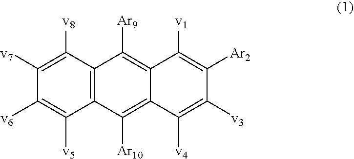


wherein Q1 and Q2 are independently selected aromatic tertiary amine moieties and G is a linking group such as an arylene, cycloalkylene, or alkylene group of a carbon to carbon bond. In one embodiment, at least one of Q1 or Q2 contains a polycyclic fused ring structure, e.g., a naphthalene. When G is an aryl group, it is conveniently a phenylene, biphenylene, or naphthalene moiety.

where
-
- R1 and R2 each independently represents a hydrogen atom, an aryl group, or an alkyl group or R1 and R2 together represent the atoms completing a cycloalkyl group; and
- R3 and R4 each independently represents an aryl group, which is in turn substituted with a diaryl substituted amino group, as indicated by structural formula (C):

wherein R5 and R6 are independently selected aryl groups. In one embodiment, at least one of R5 or R6 contains a polycyclic fused ring structure, e.g., a naphthalene.

wherein
-
- each Are is an independently selected arylene group, such as a phenylene or anthracene moiety,
- n is an integer of from 1 to 4, and
- Ar, R7, R8, and R9 are independently selected aryl groups.
-
- 1,1-Bis(4-di-p-tolylaminophenyl)cyclohexane (TAPC)
- 1,1-Bis(4-di-p-tolylaminophenyl)-4-methylcyclohexane
- 1,1-Bis(4-di-p-tolylaminophenyl)-4-phenylcyclohexane
- 1,1-Bis(4-di-p-tolylaminophenyl)-3-phenylpropane (TAPPP)
- N,N,N′,N′-tetraphenyl-4,4′″-diamino-1,1′:4′,1″:4″,1′″-quaterphenyl
- Bis(4-dimethylamino-2-methylphenyl)phenylmethane
- 1,4-bis[2-[4-[N,N-di(p-toly)amino]phenyl]vinyl]benzene (BDTAPVB)
- N,N,N′,N′-Tetra-p-tolyl-4,4′-diaminobiphenyl (TTB)
- N,N,N′,N′-Tetraphenyl-4,4′-diaminobiphenyl
- N,N,N′,N′-tetra-1-naphthyl-4,4′-diaminobiphenyl
- N,N,N′,N′-tetra-2-naphthyl-4,4′-diaminobiphenyl
- N-Phenylcarbazole
- 4,4′-Bis[N-(1-naphthyl)-N-phenylamino]biphenyl (NPB)
- 4,4′-Bis[N-(1-naphthyl)-N-(2-naphthyl)amino]biphenyl (TNB)
- 4,4′-Bis[N-(1-naphthyl)-N-phenylamino]p-terphenyl
- 4,4′-Bis[N-(2-naphthyl)-N-phenylamino]biphenyl
- 4,4′-Bis[N-(3-acenaphthenyl)-N-phenylamino]biphenyl
- 1,5-Bis[N-(1-naphthyl)-N-phenylamino]naphthalene
- 4,4′-Bis[N-(9-anthryl)-N-phenylamino]biphenyl
- 4,4′-Bis[N-(1-anthryl)-N-phenylamino]-p-terphenyl
- 4,4′-Bis[N-(2-phenanthryl)-N-phenylamino]biphenyl
- 4,4′-Bis[N-(8-fluoranthenyl)-N-phenylamino]biphenyl
- 4,4′-Bis[N-(2-pyrenyl)-N-phenylamino]biphenyl
- 4,4′-Bis[N-(2-naphthacenyl)-N-phenylamino]biphenyl
- 4,4′-Bis[N-(2-perylenyl)-N-phenylamino]biphenyl
- 4,4′-Bis[N-(1-coronenyl)-N-phenylamino]biphenyl
- 2,6-Bis(di-p-tolylamino)naphthalene
- 2,6-Bis[di-(1-naphthyl)amino]naphthalene
- 2,6-Bis[N-(1-naphthyl)-N-(2-naphthyl)amino]naphthalene
- N,N,N′,N′-Tetra(2-naphthyl)-4,4″-diamino-p-terphenyl
- 4,4′-Bis{N-phenyl-N-[4-(1-naphthyl)-phenyl]amino}biphenyl
- 2,6-Bis[N,N-di(2-naphthyl)amino]fluorene
- 4,4′,4″-tris[(3-methylphenyl)phenylamino]triphenylamine (MTDATA)
- 4,4′-Bis[N-(3-methylphenyl)-N-phenylamino]biphenyl (TPD)

wherein
-
- M represents a metal;
- n is an integer of from 1 to 4; and
- Z independently in each occurrence represents the atoms completing a nucleus having at least two fused aromatic rings.
-
- CO-1: Aluminum trisoxine [alias, tris(8-quinolinolato)aluminum(III)]
- CO-2: Magnesium bisoxine [alias, bis(8-quinolinolato)magnesium(II)]
- CO-3: Bis[benzo{f}-8-quinolinolato]zinc (II)
- CO-4: Bis(2-methyl-8-quinolinolato)aluminum(III)-μ-oxo-bis(2-methyl-8-quinolinolato) aluminum(III)
- CO-5: Indium trisoxine [alias, tris(8-quinolinolato)indium]
- CO-6: Aluminum tris(5-methyloxine) [alias, tris(5-methyl-8-quinolinolato) aluminum(III)]
- CO-7: Lithium oxine [alias, (8-quinolinolato)lithium(I)]
- CO-8: Gallium oxine [alias, tris(8-quinolinolato)gallium(III)]
- CO-9: Zirconium oxine [alias, tetra(8-quinolinolato)zirconium(IV)]

wherein: R1, R2, R3, R4, R5, and R6 represent one or more substituents on each ring where each substituent is individually selected from the following groups:
-
- Group 1: hydrogen, or alkyl of from 1 to 24 carbon atoms;
- Group 2: aryl or substituted aryl of from 5 to 20 carbon atoms;
- Group 3: carbon atoms from 4 to 24 necessary to complete a fused aromatic ring of anthracenyl; pyrenyl, or perylenyl;
- Group 4: heteroaryl or substituted heteroaryl of from 5 to 24 carbon atoms as necessary to complete a fused heteroaromatic ring of furyl, thienyl, pyridyl, quinolinyl or other heterocyclic systems;
- Group 5: alkoxylamino, alkylamino, or arylamino of from 1 to 24 carbon atoms; and
- Group 6: fluorine, chlorine, bromine or cyano.

wherein:
-
- n is an integer of 3 to 8;
- Z is O, NR or S; and
- R and R′ are individually hydrogen; alkyl of from 1 to 24 carbon atoms, for example, propyl, t-butyl, heptyl, and the like; aryl or hetero-atom substituted aryl of from 5 to 20 carbon atoms for example phenyl and naphthyl, furyl, thienyl, pyridyl, quinolinyl and other heterocyclic systems; or halo such as chloro, fluoro; or atoms necessary to complete a fused aromatic ring; and
- L is a linkage unit consisting of alkyl, aryl, substituted alkyl, or substituted aryl, which connects the multiple benzazoles together. L may be either conjugated with the multiple benzazoles or not in conjugation with them. An example of a useful benzazole is 2,2′,2″-(1,3,5-phenylene)tris[1-phenyl-1H-benzimidazole].
- Styrylarylene derivatives as described in U.S. Pat. No. 5,121,029 and JP 08333569 are also useful hosts for blue emission. For example, 9,10-bis[4-(2,2-diphenylethenyl)phenyl]anthracene and 4,4′-bis(2,2-diphenylethenyl)-1,1′-biphenyl (DPVBi) are useful hosts for blue emission.
 |
| L1 |
 |
| L2 |
 |
| L3 |
 |
| L4 |
 |
| L5 |
 |
| L6 |
 |
| L7 |
 |
| L8 |
 |
| X | R1 | R2 | |||
| L9 | O | H | H | ||
| L10 | O | H | Methyl | ||
| L11 | O | Methyl | H | ||
| L12 | O | Methyl | Methyl | ||
| L13 | O | H | t-butyl | ||
| L14 | O | t-butyl | H | ||
| L15 | O | t-butyl | t-butyl | ||
| L16 | S | H | H | ||
| L17 | S | H | Methyl | ||
| L18 | S | Methyl | H | ||
| L19 | S | Methyl | Methyl | ||
| L20 | S | H | t-butyl | ||
| L21 | S | t-butyl | H | ||
| L22 | S | t-butyl | t-butyl | ||
 |
| X | R1 | R2 | |||
| L23 | O | H | H | ||
| L24 | O | H | Methyl | ||
| L25 | O | Methyl | H | ||
| L26 | O | Methyl | Methyl | ||
| L27 | O | H | t-butyl | ||
| L28 | O | t-butyl | H | ||
| L29 | O | t-butyl | t-butyl | ||
| L30 | S | H | H | ||
| L31 | S | H | Methyl | ||
| L32 | S | Methyl | H | ||
| L33 | S | Methyl | Methyl | ||
| L34 | S | H | t-butyl | ||
| L35 | S | t-butyl | H | ||
| L36 | S | t-butyl | t-butyl | ||
 |
| R | |||
| L37 | phenyl | ||
| L38 | methyl | ||
| L39 | t-butyl | ||
| L40 | mesityl | ||
 |
| R | |||
| L41 | phenyl | ||
| L42 | methyl | ||
| L43 | t-butyl | ||
| L44 | mesityl | ||
 |
| L45 |
 |
| L46 |
 |
| L47 |
 |
| L48 |
 |
| L49 |
 |
| L50 |
 |
| L51 |
 |
| L52 |


-
- 1. A glass substrate coated with an 85 nm layer of indium-tin oxide (ITO) as the anode was sequentially ultrasonicated in a commercial detergent, rinsed in deionized water, degreased in toluene vapor and exposed to oxygen plasma for about 1 min.
- 2. Over the ITO was deposited a 1 nm fluorocarbon (CFx) hole-injecting layer (HIL) by plasma-assisted deposition of CHF3.
- 3. A hole-transporting layer (HTL) of N,N′-di-1-naphthyl-N,N-diphenyl-4,4′-diaminobiphenyl (NPB) having a thickness of 75 nm was then evaporated from a tantalum boat.
- 4. A 20 nm light-emitting layer (LEL), including host material Inv-1 and light-emitting material TBP (2,5,8,11-tetra-t-butylperylene, 1.00 vol %), was then deposited onto the hole-transporting layer. These materials were also evaporated from tantalum boats.
- 5. A 35 nm electron-transporting layer (ETL) of tris(8-quinolinolato)aluminum (III) (AlQ3) was then deposited onto the light-emitting layer. This material was also evaporated from a tantalum boat.
- 6. On top of the AlQ3 layer was deposited a 220 nm cathode formed of a 10:1 volume ratio of Mg and Ag.
| TABLE 1 |
| Evaluation Results for EL devices 1-6. |
| TBP | ||||||||
| Host | Level | Yield | 250 h | |||||
| Sam- | Level | (vol | (cd/ | Sta- | ||||
| ple | Host | (nm) | %) | A) | CIEx | CIEy | bility | Type |
| 1 | Inv-1 | 200 | 1.00 | 3.70 | 0.176 | 0.283 | 78% | Invention |
| 2 | Inv-1 | 400 | 1.00 | 4.18 | 0.184 | 0.333 | 77% | Invention |
| 3 | Inv-1 | 200 | 2.00 | 3.66 | 0.174 | 0.280 | 83% | Invention |
| 4 | Inv-1 | 400 | 2.00 | 3.89 | 0.180 | 0.328 | 81% | Invention |
| 5 | Inv-1 | 200 | 4.00 | 3.30 | 0.177 | 0.296 | 81% | Invention |
| 6 | TBADN | 200 | 1.50 | 2.40 | 0.144 | 0.184 | 71% | Com- |
| parison | ||||||||
| TABLE 2 |
| Evaluation Results for EL devices 7-12. |
| TBP | ||||||||
| Host | Level | Yield | 200 h | |||||
| Sam- | Level | (vol | (cd/ | Sta- | ||||
| ple | Host | (nm) | %) | A) | CIEx | CIEy | bility | Type |
| 7 | Inv-2 | 200 | 1.00 | 3.35 | 0.164 | 0.264 | 86% | Invention |
| 8 | Inv-2 | 400 | 1.00 | 3.27 | 0.174 | 0.321 | 84% | Invention |
| 9 | Inv-2 | 200 | 2.00 | 2.88 | 0.165 | 0.257 | 89% | Invention |
| 10 | Inv-2 | 400 | 2.00 | 3.30 | 0.175 | 0.329 | 87% | Invention |
| 11 | Inv-2 | 200 | 4.00 | 1.71 | 0.311 | 0.538 | 80% | Invention |
| 12 | TBADN | 200 | 1.50 | 2.86 | 0.144 | 0.217 | 83% | Com- |
| parison | ||||||||
| TABLE 3 |
| Evaluation Results for EL devices 13-18. |
| TBP | ||||||||
| Host | Level | Yield | 200 h | |||||
| Sam- | Level | (vol | (cd/ | Sta- | ||||
| ple | Host | (nm) | %) | A) | CIEx | CIEy | bility | Type |
| 13 | Inv-3 | 200 | 1.00 | 3.52 | 0.170 | 0.285 | 88% | Invention |
| 14 | Inv-3 | 400 | 1.00 | 4.26 | 0.174 | 0.328 | 87% | Invention |
| 15 | Inv-3 | 200 | 2.00 | 3.44 | 0.170 | 0.285 | 91% | Invention |
| 16 | Inv-3 | 400 | 2.00 | 4.14 | 0.175 | 0.335 | 89% | Invention |
| 17 | Inv-3 | 200 | 4.00 | 3.15 | 0.177 | 0.309 | 89% | Invention |
| 18 | TBADN | 200 | 1.50 | 2.87 | 0.142 | 0.205 | 75% | Com- |
| parison | ||||||||
| TABLE 4 |
| Evaluation Results for EL devices 19-24. |
| TBP | ||||||||
| Host | Level | Yield | 200 h | |||||
| Sam- | Level | (vol | (cd/ | Sta- | ||||
| ple | Host | (nm) | %) | A) | CIEx | CIEy | bility | Type |
| 19 | Inv-4 | 200 | 1.00 | 3.51 | 0.172 | 0.270 | 72% | Invention |
| 20 | Inv-4 | 400 | 1.00 | 4.46 | 0.189 | 0.371 | 70% | Invention |
| 21 | Inv-4 | 200 | 2.00 | 3.47 | 0.173 | 0.277 | 75% | Invention |
| 22 | Inv-4 | 400 | 2.00 | 3.67 | 0.182 | 0.337 | 77% | Invention |
| 23 | Inv-4 | 200 | 4.00 | 3.46 | 0.176 | 0.312 | 75% | Invention |
| 24 | TBADN | 200 | 1.50 | 2.47 | 0.144 | 0.184 | 74% | Com- |
| parison | ||||||||
| TABLE 5 |
| Evaluation Results for EL devices 25-30. |
| TBP | ||||||||
| Host | Level | Yield | 250 h | |||||
| Sam- | Level | (vol | (cd/ | Sta- | ||||
| ple | Host | (nm) | %) | A) | CIEx | CIEy | bility | Type |
| 25 | Inv-5 | 200 | 1.00 | 3.43 | 0.161 | 0.250 | 86% | Invention |
| 26 | Inv-5 | 400 | 1.00 | 4.33 | 0.163 | 0.296 | 86% | Invention |
| 27 | Inv-5 | 200 | 2.00 | 3.40 | 0.160 | 0.254 | 88% | Invention |
| 28 | Inv-5 | 400 | 2.00 | 4.06 | 0.162 | 0.299 | 87% | Invention |
| 29 | Inv-5 | 200 | 4.00 | 3.15 | 0.165 | 0.275 | 86% | Invention |
| 30 | TBADN | 200 | 1.50 | 2.85 | 0.141 | 0.191 | 79% | Com- |
| parison | ||||||||
| TABLE 6 |
| Evaluation Results for EL devices 31-36. |
| TBP | ||||||||
| Host | Level | Yield | 200 h | |||||
| Sam- | Level | (vol | (cd/ | Sta- | ||||
| ple | Host | (nm) | %) | A) | CIEx | CIEy | bility | Type |
| 31 | Inv-7 | 200 | 1.00 | 3.53 | 0.168 | 0.252 | 78% | Invention |
| 32 | Inv-7 | 400 | 1.00 | 3.96 | 0.176 | 0.319 | 76% | Invention |
| 33 | Inv-7 | 200 | 2.00 | 3.42 | 0.166 | 0.250 | 81% | Invention |
| 34 | Inv-7 | 400 | 2.00 | 3.71 | 0.171 | 0.310 | 78% | Invention |
| 35 | Inv-7 | 200 | 4.00 | 3.21 | 0.166 | 0.260 | 81% | Invention |
| 36 | TBADN | 200 | 1.50 | 2.49 | 0.145 | 0.181 | 77% | Com- |
| parison | ||||||||
| TABLE 7 |
| Evaluation Results for EL devices 37-42. |
| TBP | ||||||||
| Host | Level | Yield | 200 h | |||||
| Sam- | Level | (vol | (cd/ | Sta- | ||||
| ple | Host | (nm) | %) | A) | CIEx | CIEy | bility | Type |
| 37 | Inv-8 | 200 | 1.00 | 3.24 | 0.161 | 0.239 | 83% | Invention |
| 38 | Inv-8 | 400 | 1.00 | 3.49 | 0.168 | 0.287 | 83% | Invention |
| 39 | Inv-8 | 200 | 2.00 | 3.49 | 0.157 | 0.252 | 86% | Invention |
| 40 | Inv-8 | 400 | 2.00 | 3.48 | 0.166 | 0.303 | 83% | Invention |
| 41 | Inv-8 | 200 | 4.00 | 2.36 | 0.178 | 0.283 | 85% | Invention |
| 42 | TBADN | 200 | 1.50 | 2.85 | 0.141 | 0.189 | 76% | Com- |
| parison | ||||||||
| TABLE 8 |
| Evaluation Results for EL devices 43-48. |
| TBP | 250 h | |||||||
| Host | Level | Yield | Sta- | |||||
| Sam- | Level | (vol | (cd/ | bility | ||||
| ple | Host | (nm) | %) | A) | CIEx | CIEy | (%) | Type |
| 43 | Inv-9 | 200 | 1.00 | 3.63 | 0.186 | 0.317 | 65% | Invention |
| 44 | Inv-9 | 400 | 1.00 | 3.15 | 0.188 | 0.296 | 84% | Invention |
| 45 | Inv-9 | 200 | 2.00 | 3.38 | 0.182 | 0.308 | 86% | Invention |
| 46 | Inv-9 | 400 | 2.00 | 3.33 | 0.187 | 0.322 | 84% | Invention |
| 47 | Inv-9 | 200 | 4.00 | 2.73 | 0.195 | 0.320 | 84% | Invention |
| 48 | TBADN | 200 | 1.50 | 2.57 | 0.144 | 0.189 | 71% | Com- |
| parison | ||||||||
- 101 Substrate
- 103 Anode
- 105 Hole-Injecting layer (HIL)
- 107 Hole-Transporting layer (HTL)
- 109 Light-Emitting layer (LEL)
- 111 Electron-Transporting layer (ETL)
- 113 Cathode
Claims (28)


Priority Applications (8)
| Application Number | Priority Date | Filing Date | Title |
|---|---|---|---|
| US10/809,064 US7326371B2 (en) | 2004-03-25 | 2004-03-25 | Electroluminescent device with anthracene derivative host |
| DE602005014951T DE602005014951D1 (en) | 2004-03-25 | 2005-03-11 | ELECTROLUMINESCENT DEVICE WITH ANTHRACEN DERIVATIVE THAN HOST |
| KR1020067019642A KR101182702B1 (en) | 2004-03-25 | 2005-03-11 | Electroluminescent device with anthracene derivative host |
| PCT/US2005/008253 WO2005100506A1 (en) | 2004-03-25 | 2005-03-11 | Electroluminescent device with anthracene derivative host |
| CN2005800094046A CN1934215B (en) | 2004-03-25 | 2005-03-11 | Electroluminescent device with anthracene derivative matrix |
| EP05725437A EP1730249B2 (en) | 2004-03-25 | 2005-03-11 | Electroluminescent device with anthracene derivative host |
| JP2007504998A JP2007531273A (en) | 2004-03-25 | 2005-03-11 | Electroluminescent device with anthracene derivative host |
| JP2011278389A JP5744713B2 (en) | 2004-03-25 | 2011-12-20 | Electroluminescent device with anthracene derivative host |
Applications Claiming Priority (1)
| Application Number | Priority Date | Filing Date | Title |
|---|---|---|---|
| US10/809,064 US7326371B2 (en) | 2004-03-25 | 2004-03-25 | Electroluminescent device with anthracene derivative host |
Publications (2)
| Publication Number | Publication Date |
|---|---|
| US20050211958A1 US20050211958A1 (en) | 2005-09-29 |
| US7326371B2 true US7326371B2 (en) | 2008-02-05 |
Family
ID=34962567
Family Applications (1)
| Application Number | Title | Priority Date | Filing Date |
|---|---|---|---|
| US10/809,064 Expired - Lifetime US7326371B2 (en) | 2004-03-25 | 2004-03-25 | Electroluminescent device with anthracene derivative host |
Country Status (7)
| Country | Link |
|---|---|
| US (1) | US7326371B2 (en) |
| EP (1) | EP1730249B2 (en) |
| JP (2) | JP2007531273A (en) |
| KR (1) | KR101182702B1 (en) |
| CN (1) | CN1934215B (en) |
| DE (1) | DE602005014951D1 (en) |
| WO (1) | WO2005100506A1 (en) |
Cited By (70)
| Publication number | Priority date | Publication date | Assignee | Title |
|---|---|---|---|---|
| US20060046097A1 (en) * | 2004-09-02 | 2006-03-02 | Kim Ji E | Anthracene derivatives and organic light emitting device using the same as a light emitting material |
| WO2010114256A2 (en) * | 2009-03-31 | 2010-10-07 | Dow Advanced Display Materials,Ltd. | Novel organic electroluminescent compounds and organic electroluminescent device using the same |
| US20100301319A1 (en) * | 2009-05-22 | 2010-12-02 | Idemitsu Kosan Co., Ltd. | Organic electroluminescent device |
| WO2011015265A2 (en) | 2009-08-04 | 2011-02-10 | Merck Patent Gmbh | Electronic devices comprising multi cyclic hydrocarbons |
| US20110101316A1 (en) * | 2009-10-29 | 2011-05-05 | E.I. Du Pont De Nemours And Company | Organic light-emitting diode luminaires |
| WO2011076326A1 (en) | 2009-12-22 | 2011-06-30 | Merck Patent Gmbh | Electroluminescent functional surfactants |
| WO2011076314A1 (en) | 2009-12-22 | 2011-06-30 | Merck Patent Gmbh | Electroluminescent formulations |
| WO2011076323A1 (en) | 2009-12-22 | 2011-06-30 | Merck Patent Gmbh | Formulations comprising phase-separated functional materials |
| DE102010009193A1 (en) | 2010-02-24 | 2011-08-25 | Merck Patent GmbH, 64293 | Fluorine-fluorine associates |
| WO2011110277A1 (en) | 2010-03-11 | 2011-09-15 | Merck Patent Gmbh | Fibers in therapy and cosmetics |
| WO2011110275A2 (en) | 2010-03-11 | 2011-09-15 | Merck Patent Gmbh | Radiative fibers |
| US20110260144A1 (en) * | 2009-10-29 | 2011-10-27 | E. I. Du Pont De Nemours And Company | Organic light-emitting diode luminaires |
| WO2011147522A1 (en) | 2010-05-27 | 2011-12-01 | Merck Patent Gmbh | Compositions comprising quantum dots |
| WO2012013270A1 (en) | 2010-07-26 | 2012-02-02 | Merck Patent Gmbh | Nanocrystals in devices |
| WO2012013272A1 (en) | 2010-07-26 | 2012-02-02 | Merck Patent Gmbh | Quantum dots and hosts |
| US20120138914A1 (en) * | 2009-05-29 | 2012-06-07 | Idemitsu Kosan Co., Ltd. | Anthracene derivative and organic electroluminescent element using the same |
| WO2012110178A1 (en) | 2011-02-14 | 2012-08-23 | Merck Patent Gmbh | Device and method for treatment of cells and cell tissue |
| WO2012126566A1 (en) | 2011-03-24 | 2012-09-27 | Merck Patent Gmbh | Organic ionic functional materials |
| WO2012152366A1 (en) | 2011-05-12 | 2012-11-15 | Merck Patent Gmbh | Organic ionic compounds, compositions and electronic devices |
| WO2013113349A1 (en) | 2012-01-30 | 2013-08-08 | Merck Patent Gmbh | Nanocrystals on fibers |
| WO2016034262A1 (en) | 2014-09-05 | 2016-03-10 | Merck Patent Gmbh | Formulations and electronic devices |
| WO2016107663A1 (en) | 2014-12-30 | 2016-07-07 | Merck Patent Gmbh | Formulations and electronic devices |
| WO2016155866A1 (en) | 2015-03-30 | 2016-10-06 | Merck Patent Gmbh | Formulation of an organic functional material comprising a siloxane solvent |
| WO2016198141A1 (en) | 2015-06-12 | 2016-12-15 | Merck Patent Gmbh | Esters containing non-aromatic cycles as solvents for oled formulations |
| WO2017036572A1 (en) | 2015-08-28 | 2017-03-09 | Merck Patent Gmbh | Formulation of an organic functional material comprising an epoxy group containing solvent |
| WO2017097391A1 (en) | 2015-12-10 | 2017-06-15 | Merck Patent Gmbh | Formulations containing ketones comprising non-aromatic cycles |
| WO2017102049A1 (en) | 2015-12-16 | 2017-06-22 | Merck Patent Gmbh | Formulations containing a mixture of at least two different solvents |
| WO2017102052A1 (en) | 2015-12-16 | 2017-06-22 | Merck Patent Gmbh | Formulations containing a solid solvent |
| WO2017102048A1 (en) | 2015-12-15 | 2017-06-22 | Merck Patent Gmbh | Esters containing aromatic groups as solvents for organic electronic formulations |
| WO2017140404A1 (en) | 2016-02-17 | 2017-08-24 | Merck Patent Gmbh | Formulation of an organic functional material |
| DE102016003104A1 (en) | 2016-03-15 | 2017-09-21 | Merck Patent Gmbh | Container comprising a formulation containing at least one organic semiconductor |
| WO2017194435A1 (en) | 2016-05-11 | 2017-11-16 | Merck Patent Gmbh | Compositions for electrochemical cells |
| WO2017216128A1 (en) | 2016-06-17 | 2017-12-21 | Merck Patent Gmbh | Formulation of an organic functional material |
| WO2017216129A1 (en) | 2016-06-16 | 2017-12-21 | Merck Patent Gmbh | Formulation of an organic functional material |
| WO2018001928A1 (en) | 2016-06-28 | 2018-01-04 | Merck Patent Gmbh | Formulation of an organic functional material |
| WO2018024719A1 (en) | 2016-08-04 | 2018-02-08 | Merck Patent Gmbh | Formulation of an organic functional material |
| WO2018077660A1 (en) | 2016-10-31 | 2018-05-03 | Merck Patent Gmbh | Formulation of an organic functional material |
| WO2018077662A1 (en) | 2016-10-31 | 2018-05-03 | Merck Patent Gmbh | Formulation of an organic functional material |
| WO2018087346A1 (en) | 2016-11-14 | 2018-05-17 | Merck Patent Gmbh | Compounds with an acceptor and a donor group |
| WO2018104202A1 (en) | 2016-12-06 | 2018-06-14 | Merck Patent Gmbh | Preparation process for an electronic device |
| WO2018108760A1 (en) | 2016-12-13 | 2018-06-21 | Merck Patent Gmbh | Formulation of an organic functional material |
| WO2018114883A1 (en) | 2016-12-22 | 2018-06-28 | Merck Patent Gmbh | Mixtures comprising at least two organofunctional compounds |
| WO2018138318A1 (en) | 2017-01-30 | 2018-08-02 | Merck Patent Gmbh | Method for forming an organic element of an electronic device |
| WO2018138319A1 (en) | 2017-01-30 | 2018-08-02 | Merck Patent Gmbh | Method for forming an organic electroluminescence (el) element |
| WO2018178136A1 (en) | 2017-03-31 | 2018-10-04 | Merck Patent Gmbh | Printing method for an organic light emitting diode (oled) |
| WO2018189050A1 (en) | 2017-04-10 | 2018-10-18 | Merck Patent Gmbh | Formulation of an organic functional material |
| WO2018202603A1 (en) | 2017-05-03 | 2018-11-08 | Merck Patent Gmbh | Formulation of an organic functional material |
| WO2019016184A1 (en) | 2017-07-18 | 2019-01-24 | Merck Patent Gmbh | Formulation of an organic functional material |
| WO2019115573A1 (en) | 2017-12-15 | 2019-06-20 | Merck Patent Gmbh | Formulation of an organic functional material |
| WO2019162483A1 (en) | 2018-02-26 | 2019-08-29 | Merck Patent Gmbh | Formulation of an organic functional material |
| WO2019238782A1 (en) | 2018-06-15 | 2019-12-19 | Merck Patent Gmbh | Formulation of an organic functional material |
| WO2020064582A1 (en) | 2018-09-24 | 2020-04-02 | Merck Patent Gmbh | Method for the production of a granular material |
| WO2020094538A1 (en) | 2018-11-06 | 2020-05-14 | Merck Patent Gmbh | Method for forming an organic element of an electronic device |
| WO2021213917A1 (en) | 2020-04-21 | 2021-10-28 | Merck Patent Gmbh | Emulsions comprising organic functional materials |
| WO2021213918A1 (en) | 2020-04-21 | 2021-10-28 | Merck Patent Gmbh | Formulation of an organic functional material |
| WO2021259824A1 (en) | 2020-06-23 | 2021-12-30 | Merck Patent Gmbh | Method for producing a mixture |
| WO2022122607A1 (en) | 2020-12-08 | 2022-06-16 | Merck Patent Gmbh | An ink system and a method for inkjet printing |
| WO2022223675A1 (en) | 2021-04-23 | 2022-10-27 | Merck Patent Gmbh | Formulation of an organic functional material |
| WO2022243403A1 (en) | 2021-05-21 | 2022-11-24 | Merck Patent Gmbh | Method for the continuous purification of at least one functional material and device for the continuous purification of at least one functional material |
| WO2023012084A1 (en) | 2021-08-02 | 2023-02-09 | Merck Patent Gmbh | A printing method by combining inks |
| US11581487B2 (en) | 2017-04-26 | 2023-02-14 | Oti Lumionics Inc. | Patterned conductive coating for surface of an opto-electronic device |
| WO2023057327A1 (en) | 2021-10-05 | 2023-04-13 | Merck Patent Gmbh | Method for forming an organic element of an electronic device |
| US11730012B2 (en) | 2019-03-07 | 2023-08-15 | Oti Lumionics Inc. | Materials for forming a nucleation-inhibiting coating and devices incorporating same |
| US11751415B2 (en) | 2018-02-02 | 2023-09-05 | Oti Lumionics Inc. | Materials for forming a nucleation-inhibiting coating and devices incorporating same |
| WO2023237458A1 (en) | 2022-06-07 | 2023-12-14 | Merck Patent Gmbh | Method of printing a functional layer of an electronic device by combining inks |
| US11985841B2 (en) | 2020-12-07 | 2024-05-14 | Oti Lumionics Inc. | Patterning a conductive deposited layer using a nucleation inhibiting coating and an underlying metallic coating |
| WO2024126635A1 (en) | 2022-12-16 | 2024-06-20 | Merck Patent Gmbh | Formulation of an organic functional material |
| US12069938B2 (en) | 2019-05-08 | 2024-08-20 | Oti Lumionics Inc. | Materials for forming a nucleation-inhibiting coating and devices incorporating same |
| US12101987B2 (en) | 2019-04-18 | 2024-09-24 | Oti Lumionics Inc. | Materials for forming a nucleation-inhibiting coating and devices incorporating same |
| WO2025032039A1 (en) | 2023-08-07 | 2025-02-13 | Merck Patent Gmbh | Process for the preparation of an electronic device |
Families Citing this family (73)
| Publication number | Priority date | Publication date | Assignee | Title |
|---|---|---|---|---|
| US20040126617A1 (en) * | 2002-12-31 | 2004-07-01 | Eastman Kodak Company | Efficient electroluminescent device |
| US7329466B2 (en) * | 2004-01-30 | 2008-02-12 | Eastman Kodak Company | Organic element for electroluminescent devices |
| US20060204783A1 (en) * | 2005-03-10 | 2006-09-14 | Conley Scott R | Organic electroluminescent device |
| US20060269782A1 (en) * | 2005-05-25 | 2006-11-30 | Eastman Kodak Company | OLED electron-transporting layer |
| US8766023B2 (en) * | 2005-07-20 | 2014-07-01 | Lg Display Co., Ltd. | Synthesis process |
| KR100788254B1 (en) | 2005-08-16 | 2007-12-27 | (주)그라쎌 | Green electroluminescent compounds and organic electroluminescent device using the same |
| KR100828173B1 (en) * | 2005-11-22 | 2008-05-08 | (주)그라쎌 | Organic Electroluminescent Compounds and Display Device using The Same |
| US9666826B2 (en) * | 2005-11-30 | 2017-05-30 | Global Oled Technology Llc | Electroluminescent device including an anthracene derivative |
| US20070252517A1 (en) * | 2006-04-27 | 2007-11-01 | Eastman Kodak Company | Electroluminescent device including an anthracene derivative |
| US20070252515A1 (en) * | 2006-04-27 | 2007-11-01 | Eastman Kodak Company | Electroluminescent device including an anthracene derivative |
| KR100893044B1 (en) * | 2006-07-26 | 2009-04-15 | 주식회사 엘지화학 | Anthracene derivative, organic electronic device using the same, and electronic device including the organic electronic device |
| WO2008056510A1 (en) * | 2006-11-08 | 2008-05-15 | Konica Minolta Holdings, Inc. | Display element |
| KR20090077831A (en) * | 2006-11-09 | 2009-07-15 | 이데미쓰 고산 가부시키가이샤 | A solution containing an organic EL material, a method of synthesizing an organic EL material, a compound synthesized by this synthesis method, a method of forming a thin film of an organic EL material, a thin film of an organic EL material, an organic EL element |
| KR100903203B1 (en) * | 2006-11-30 | 2009-06-18 | 에스에프씨 주식회사 | Anthracene Derivatives and Organic Electroluminescent Devices Employing the Same |
| TWI502049B (en) * | 2006-12-28 | 2015-10-01 | Semiconductor Energy Lab | Organic compound and method for synthesizing organic compound and anthracene derivative |
| US8795855B2 (en) * | 2007-01-30 | 2014-08-05 | Global Oled Technology Llc | OLEDs having high efficiency and excellent lifetime |
| EP2444470B1 (en) | 2007-08-31 | 2016-10-26 | Semiconductor Energy Laboratory Co., Ltd. | Light-emitting element, light-emitting device, and electronic appliance |
| KR100935356B1 (en) * | 2007-11-19 | 2010-01-06 | 다우어드밴스드디스플레이머티리얼 유한회사 | Green light emitting compound and organic electroluminescent device employing the same as light emitting material |
| KR100940938B1 (en) * | 2007-12-04 | 2010-02-08 | 다우어드밴스드디스플레이머티리얼 유한회사 | Novel organic light emitting compound and organic electroluminescent device employing it as light emitting material |
| JP4662384B2 (en) * | 2007-12-25 | 2011-03-30 | 財団法人山形県産業技術振興機構 | Organic electroluminescent material and device using the same |
| KR100991416B1 (en) * | 2007-12-31 | 2010-11-03 | 다우어드밴스드디스플레이머티리얼 유한회사 | Organic light emitting compound and organic light emitting device comprising the same |
| KR100974562B1 (en) * | 2007-12-31 | 2010-08-06 | 다우어드밴스드디스플레이머티리얼 유한회사 | Novel organic light emitting compound and organic light emitting device employing the same as light emitting material |
| KR101001384B1 (en) * | 2008-02-29 | 2010-12-14 | 다우어드밴스드디스플레이머티리얼 유한회사 | Novel organic light emitting compound and organic electroluminescent device employing it as light emitting material |
| KR100901887B1 (en) * | 2008-03-14 | 2009-06-09 | (주)그라쎌 | Novel organic light emitting compound and organic light emitting device employing the same |
| KR100989815B1 (en) * | 2008-03-20 | 2010-10-29 | 다우어드밴스드디스플레이머티리얼 유한회사 | Novel organic light emitting compound and organic light emitting device employing the same as light emitting material |
| KR100946411B1 (en) * | 2008-03-28 | 2010-03-09 | 다우어드밴스드디스플레이머티리얼 유한회사 | Novel organic light emitting compound and organic light emitting device employing the same as light emitting material |
| KR100910150B1 (en) * | 2008-04-02 | 2009-08-03 | (주)그라쎌 | Novel organic light emitting compound and organic light emitting device employing the same as light emitting material |
| KR101495547B1 (en) * | 2008-04-17 | 2015-02-25 | 롬엔드하스전자재료코리아유한회사 | Novel compounds for electronic material and organic electronic device using the same |
| KR20090111915A (en) * | 2008-04-23 | 2009-10-28 | (주)그라쎌 | Novel organic light emitting compound and organic light emitting device employing the same as light emitting material |
| WO2009154207A1 (en) * | 2008-06-17 | 2009-12-23 | 出光興産株式会社 | Anthracene derivative and organic electroluminescent element using the same |
| KR20100000772A (en) * | 2008-06-25 | 2010-01-06 | 다우어드밴스드디스플레이머티리얼 유한회사 | Novel organic electroluminescent compounds and organic electroluminescent device using the same |
| EP2145936A3 (en) * | 2008-07-14 | 2010-03-17 | Gracel Display Inc. | Fluorene and pyrene derivatives and organic electroluminescent device using the same |
| KR20100041043A (en) * | 2008-10-13 | 2010-04-22 | 다우어드밴스드디스플레이머티리얼 유한회사 | Novel organic electroluminescent compounds and organic electroluminescent device using the same |
| DE102009005746A1 (en) | 2009-01-23 | 2010-07-29 | Merck Patent Gmbh | Materials for organic electroluminescent devices |
| DE102009009277B4 (en) | 2009-02-17 | 2023-12-07 | Merck Patent Gmbh | Organic electronic device, process for its production and use of compounds |
| JP2012530819A (en) | 2009-06-22 | 2012-12-06 | メルク パテント ゲーエムベーハー | Conductive formulation |
| US8877356B2 (en) * | 2009-07-22 | 2014-11-04 | Global Oled Technology Llc | OLED device with stabilized yellow light-emitting layer |
| DE102009042693A1 (en) | 2009-09-23 | 2011-03-24 | Merck Patent Gmbh | Materials for electronic devices |
| DE102009053191A1 (en) | 2009-11-06 | 2011-05-12 | Merck Patent Gmbh | Materials for electronic devices |
| KR20170091788A (en) | 2009-12-23 | 2017-08-09 | 메르크 파텐트 게엠베하 | Compositions comprising polymeric binders |
| JP5840621B2 (en) | 2009-12-23 | 2016-01-06 | メルク パテント ゲーエムベーハー | Composition comprising organic semiconductor compound |
| DE102010005697A1 (en) | 2010-01-25 | 2011-07-28 | Merck Patent GmbH, 64293 | Connections for electronic devices |
| DE102010009903A1 (en) | 2010-03-02 | 2011-09-08 | Merck Patent Gmbh | Connections for electronic devices |
| DE102010013068A1 (en) | 2010-03-26 | 2011-09-29 | Merck Patent Gmbh | Connections for electronic devices |
| KR101896723B1 (en) | 2010-04-12 | 2018-09-07 | 메르크 파텐트 게엠베하 | Composition and method for preparation of organic electronic devices |
| KR102045196B1 (en) | 2010-04-12 | 2019-11-15 | 메르크 파텐트 게엠베하 | Composition having improved performance |
| CN102906216B (en) | 2010-05-27 | 2016-03-09 | 默克专利股份有限公司 | The method of composition and production organic electronic device |
| DE102010024335A1 (en) | 2010-06-18 | 2011-12-22 | Merck Patent Gmbh | Connections for electronic devices |
| DE102010024542A1 (en) | 2010-06-22 | 2011-12-22 | Merck Patent Gmbh | Materials for electronic devices |
| DE102010033548A1 (en) | 2010-08-05 | 2012-02-09 | Merck Patent Gmbh | Materials for electronic devices |
| DE102010048074A1 (en) | 2010-10-09 | 2012-04-12 | Merck Patent Gmbh | Materials for electronic devices |
| DE102010048607A1 (en) | 2010-10-15 | 2012-04-19 | Merck Patent Gmbh | Connections for electronic devices |
| US9627626B2 (en) | 2011-01-13 | 2017-04-18 | Merck Patent Gmbh | Compounds for organic electroluminescent devices |
| DE102011011539A1 (en) | 2011-02-17 | 2012-08-23 | Merck Patent Gmbh | Connections for electronic devices |
| US9768385B2 (en) | 2011-04-13 | 2017-09-19 | Merck Patent Gmbh | Compounds for electronic devices |
| WO2012139692A1 (en) | 2011-04-13 | 2012-10-18 | Merck Patent Gmbh | Materials for electronic devices |
| JP6022541B2 (en) | 2011-04-18 | 2016-11-09 | メルク パテント ゲーエムベーハー | Compounds for electronic devices |
| WO2012149992A1 (en) | 2011-05-04 | 2012-11-08 | Merck Patent Gmbh | Device for preserving fresh goods |
| EP2782975B1 (en) | 2011-10-27 | 2018-01-10 | Merck Patent GmbH | Materials for electronic devices |
| CN104114672B (en) | 2012-02-14 | 2017-03-15 | 默克专利有限公司 | Two fluorene compound of spiral shell for organic electroluminescence device |
| JP2013207139A (en) * | 2012-03-29 | 2013-10-07 | Kaneka Corp | Luminescent material and organic el element |
| JP6716457B2 (en) | 2013-12-06 | 2020-07-01 | メルク パテント ゲーエムベーハー | Compositions containing polymeric binders containing acrylate and/or methacrylate units |
| JP7030519B2 (en) | 2015-01-30 | 2022-03-07 | メルク パテント ゲーエムベーハー | Formulations with low particle content |
| JP7019559B2 (en) | 2015-07-15 | 2022-02-15 | メルク パテント ゲーエムベーハー | Compositions containing organic semiconductor compounds |
| EP3147961A1 (en) * | 2015-09-28 | 2017-03-29 | Novaled GmbH | Organic electroluminescent device |
| TWI813576B (en) | 2017-07-03 | 2023-09-01 | 德商麥克專利有限公司 | Formulations with a low content of phenol type impurities |
| KR102072922B1 (en) | 2017-10-30 | 2020-02-10 | 주식회사 엘지화학 | Hetero-cyclic compound and organic light emitting device comprising same |
| KR102186088B1 (en) | 2017-11-16 | 2020-12-03 | 주식회사 엘지화학 | Polycyclic compound and organic light emitting device comprising the same |
| US12029055B2 (en) | 2018-01-30 | 2024-07-02 | The University Of Southern California | OLED with hybrid emissive layer |
| US11780829B2 (en) | 2019-01-30 | 2023-10-10 | The University Of Southern California | Organic electroluminescent materials and devices |
| US11812624B2 (en) * | 2019-01-30 | 2023-11-07 | The University Of Southern California | Organic electroluminescent materials and devices |
| US20220302392A1 (en) * | 2019-11-05 | 2022-09-22 | Lg Chem, Ltd. | Organic light emitting device |
| JP2021103714A (en) * | 2019-12-25 | 2021-07-15 | 出光興産株式会社 | Organic electroluminescence device and electronic equipment |
Citations (20)
| Publication number | Priority date | Publication date | Assignee | Title |
|---|---|---|---|---|
| JPH113782A (en) | 1997-06-12 | 1999-01-06 | Toppan Printing Co Ltd | El element of organic thin film |
| US5972247A (en) | 1998-03-20 | 1999-10-26 | Eastman Kodak Company | Organic electroluminescent elements for stable blue electroluminescent devices |
| JPH11297473A (en) | 1998-04-15 | 1999-10-29 | Nec Corp | Organic electroluminescence element |
| JPH11323323A (en) | 1998-05-20 | 1999-11-26 | Toppan Printing Co Ltd | Luminescent material |
| EP1094101A2 (en) | 1999-10-20 | 2001-04-25 | Eastman Kodak Company | Electroluminescent devices having naphthylanthracene-based polymers |
| US20020027416A1 (en) * | 2000-03-27 | 2002-03-07 | Dong-Hyun Kim | Organic electroluminescent device including charge transport buffer layer |
| US6361886B2 (en) * | 1998-12-09 | 2002-03-26 | Eastman Kodak Company | Electroluminescent device with improved hole transport layer |
| US6582837B1 (en) | 1997-07-14 | 2003-06-24 | Nec Corporation | Organic electroluminescence device |
| WO2003060956A2 (en) | 2002-01-18 | 2003-07-24 | Lg Chem, Ltd. | New material for transporting electrons and organic electroluminescent display using the same |
| US6661023B2 (en) * | 2002-02-28 | 2003-12-09 | Eastman Kodak Company | Organic element for electroluminescent devices |
| US6670053B2 (en) * | 2002-02-26 | 2003-12-30 | Eastman Kodak Company | Organic electroluminescent devices with high luminance |
| US20040001969A1 (en) * | 2002-06-27 | 2004-01-01 | Eastman Kodak Company | Device containing green organic light-emitting diode |
| US20040023060A1 (en) | 2001-04-27 | 2004-02-05 | Kim Kong Kyeom | Double-spiro organic compounds and organic electroluminescent devices using the same |
| JP2004059535A (en) | 2002-07-31 | 2004-02-26 | Idemitsu Kosan Co Ltd | Anthracene derivative, light emitting material for organic electroluminescent device, and organic electroluminescent device |
| WO2004018587A1 (en) | 2002-08-23 | 2004-03-04 | Idemitsu Kosan Co., Ltd. | Organic electroluminescence device and anthracene derivative |
| US6828044B2 (en) * | 2002-10-25 | 2004-12-07 | Eastman Kodak Company | Dopant in an electroluminescent device |
| US20050058853A1 (en) * | 2003-09-15 | 2005-03-17 | Eastman Kodak Company | Green organic light-emitting diodes |
| US20050181232A1 (en) * | 2004-02-17 | 2005-08-18 | Eastman Kodak Company | Anthracene derivative host having ranges of dopants |
| US20050208329A1 (en) * | 2004-03-18 | 2005-09-22 | Eastman Kodak Company | Organic element for electroluminescent devices |
| US6984459B1 (en) * | 1999-08-03 | 2006-01-10 | Sumito Chemical Company, Limited | Polymeric fluorescent substance and polymer light emitting device |
Family Cites Families (2)
| Publication number | Priority date | Publication date | Assignee | Title |
|---|---|---|---|---|
| JP2000053676A (en) * | 1998-08-10 | 2000-02-22 | Idemitsu Kosan Co Ltd | Aromatic hydrocarbon compound and organic electroluminescent device using the same |
| JP2005170911A (en) * | 2003-12-15 | 2005-06-30 | Idemitsu Kosan Co Ltd | Aromatic compound and organic electroluminescence device using the same |
-
2004
- 2004-03-25 US US10/809,064 patent/US7326371B2/en not_active Expired - Lifetime
-
2005
- 2005-03-11 CN CN2005800094046A patent/CN1934215B/en not_active Expired - Lifetime
- 2005-03-11 KR KR1020067019642A patent/KR101182702B1/en active IP Right Grant
- 2005-03-11 EP EP05725437A patent/EP1730249B2/en not_active Expired - Lifetime
- 2005-03-11 DE DE602005014951T patent/DE602005014951D1/en not_active Expired - Lifetime
- 2005-03-11 JP JP2007504998A patent/JP2007531273A/en active Pending
- 2005-03-11 WO PCT/US2005/008253 patent/WO2005100506A1/en not_active Application Discontinuation
-
2011
- 2011-12-20 JP JP2011278389A patent/JP5744713B2/en not_active Expired - Lifetime
Patent Citations (21)
| Publication number | Priority date | Publication date | Assignee | Title |
|---|---|---|---|---|
| JPH113782A (en) | 1997-06-12 | 1999-01-06 | Toppan Printing Co Ltd | El element of organic thin film |
| US6582837B1 (en) | 1997-07-14 | 2003-06-24 | Nec Corporation | Organic electroluminescence device |
| US5972247A (en) | 1998-03-20 | 1999-10-26 | Eastman Kodak Company | Organic electroluminescent elements for stable blue electroluminescent devices |
| JPH11297473A (en) | 1998-04-15 | 1999-10-29 | Nec Corp | Organic electroluminescence element |
| JPH11323323A (en) | 1998-05-20 | 1999-11-26 | Toppan Printing Co Ltd | Luminescent material |
| US6361886B2 (en) * | 1998-12-09 | 2002-03-26 | Eastman Kodak Company | Electroluminescent device with improved hole transport layer |
| US6984459B1 (en) * | 1999-08-03 | 2006-01-10 | Sumito Chemical Company, Limited | Polymeric fluorescent substance and polymer light emitting device |
| US6361887B1 (en) * | 1999-10-20 | 2002-03-26 | Eastman Kodak Company | Electroluminescent devices having naphthylanthracene-based polymers |
| EP1094101A2 (en) | 1999-10-20 | 2001-04-25 | Eastman Kodak Company | Electroluminescent devices having naphthylanthracene-based polymers |
| US20020027416A1 (en) * | 2000-03-27 | 2002-03-07 | Dong-Hyun Kim | Organic electroluminescent device including charge transport buffer layer |
| US20040023060A1 (en) | 2001-04-27 | 2004-02-05 | Kim Kong Kyeom | Double-spiro organic compounds and organic electroluminescent devices using the same |
| WO2003060956A2 (en) | 2002-01-18 | 2003-07-24 | Lg Chem, Ltd. | New material for transporting electrons and organic electroluminescent display using the same |
| US6670053B2 (en) * | 2002-02-26 | 2003-12-30 | Eastman Kodak Company | Organic electroluminescent devices with high luminance |
| US6661023B2 (en) * | 2002-02-28 | 2003-12-09 | Eastman Kodak Company | Organic element for electroluminescent devices |
| US20040001969A1 (en) * | 2002-06-27 | 2004-01-01 | Eastman Kodak Company | Device containing green organic light-emitting diode |
| JP2004059535A (en) | 2002-07-31 | 2004-02-26 | Idemitsu Kosan Co Ltd | Anthracene derivative, light emitting material for organic electroluminescent device, and organic electroluminescent device |
| WO2004018587A1 (en) | 2002-08-23 | 2004-03-04 | Idemitsu Kosan Co., Ltd. | Organic electroluminescence device and anthracene derivative |
| US6828044B2 (en) * | 2002-10-25 | 2004-12-07 | Eastman Kodak Company | Dopant in an electroluminescent device |
| US20050058853A1 (en) * | 2003-09-15 | 2005-03-17 | Eastman Kodak Company | Green organic light-emitting diodes |
| US20050181232A1 (en) * | 2004-02-17 | 2005-08-18 | Eastman Kodak Company | Anthracene derivative host having ranges of dopants |
| US20050208329A1 (en) * | 2004-03-18 | 2005-09-22 | Eastman Kodak Company | Organic element for electroluminescent devices |
Cited By (87)
| Publication number | Priority date | Publication date | Assignee | Title |
|---|---|---|---|---|
| US20060046097A1 (en) * | 2004-09-02 | 2006-03-02 | Kim Ji E | Anthracene derivatives and organic light emitting device using the same as a light emitting material |
| WO2010114256A2 (en) * | 2009-03-31 | 2010-10-07 | Dow Advanced Display Materials,Ltd. | Novel organic electroluminescent compounds and organic electroluminescent device using the same |
| WO2010114256A3 (en) * | 2009-03-31 | 2010-12-16 | Dow Advanced Display Materials,Ltd. | Novel organic electroluminescent compounds and organic electroluminescent device using the same |
| US20100301319A1 (en) * | 2009-05-22 | 2010-12-02 | Idemitsu Kosan Co., Ltd. | Organic electroluminescent device |
| US9153790B2 (en) | 2009-05-22 | 2015-10-06 | Idemitsu Kosan Co., Ltd. | Organic electroluminescent device |
| US8629430B2 (en) * | 2009-05-29 | 2014-01-14 | Idemitsu Kosan Co., Ltd. | Anthracene derivative and organic electroluminescent element using the same |
| US8866135B2 (en) | 2009-05-29 | 2014-10-21 | Idemitsu Kosan Co., Ltd. | Anthracene derivative and organic electroluminescent element using the same |
| US20120138914A1 (en) * | 2009-05-29 | 2012-06-07 | Idemitsu Kosan Co., Ltd. | Anthracene derivative and organic electroluminescent element using the same |
| US9147847B2 (en) | 2009-05-29 | 2015-09-29 | Idemitsu Kosan Co., Ltd. | Anthracene derivative and organic electroluminescent element using the same |
| US9373792B2 (en) | 2009-05-29 | 2016-06-21 | Idemitsu Kosan Co., Ltd. | Anthracene derivative and organic electroluminescent element using the same |
| WO2011015265A2 (en) | 2009-08-04 | 2011-02-10 | Merck Patent Gmbh | Electronic devices comprising multi cyclic hydrocarbons |
| US20110101316A1 (en) * | 2009-10-29 | 2011-05-05 | E.I. Du Pont De Nemours And Company | Organic light-emitting diode luminaires |
| US20110260144A1 (en) * | 2009-10-29 | 2011-10-27 | E. I. Du Pont De Nemours And Company | Organic light-emitting diode luminaires |
| US8716700B2 (en) * | 2009-10-29 | 2014-05-06 | E I Du Pont De Nemours And Company | Organic light-emitting diodes having white light emission |
| US8716699B2 (en) | 2009-10-29 | 2014-05-06 | E I Du Pont De Nemours And Company | Organic light-emitting diodes having white light emission |
| WO2011076323A1 (en) | 2009-12-22 | 2011-06-30 | Merck Patent Gmbh | Formulations comprising phase-separated functional materials |
| WO2011076314A1 (en) | 2009-12-22 | 2011-06-30 | Merck Patent Gmbh | Electroluminescent formulations |
| WO2011076326A1 (en) | 2009-12-22 | 2011-06-30 | Merck Patent Gmbh | Electroluminescent functional surfactants |
| DE102010009193B4 (en) | 2010-02-24 | 2022-05-19 | MERCK Patent Gesellschaft mit beschränkter Haftung | Composition containing fluorine-fluorine associates, processes for their production, their use and organic electronic devices containing them |
| WO2011103953A1 (en) | 2010-02-24 | 2011-09-01 | Merck Patent Gmbh | Fluorine-fluorine associates |
| DE102010009193A1 (en) | 2010-02-24 | 2011-08-25 | Merck Patent GmbH, 64293 | Fluorine-fluorine associates |
| WO2011110277A1 (en) | 2010-03-11 | 2011-09-15 | Merck Patent Gmbh | Fibers in therapy and cosmetics |
| WO2011110275A2 (en) | 2010-03-11 | 2011-09-15 | Merck Patent Gmbh | Radiative fibers |
| WO2011147522A1 (en) | 2010-05-27 | 2011-12-01 | Merck Patent Gmbh | Compositions comprising quantum dots |
| EP3309236A1 (en) | 2010-05-27 | 2018-04-18 | Merck Patent GmbH | Compositions comprising quantum dots |
| WO2012013272A1 (en) | 2010-07-26 | 2012-02-02 | Merck Patent Gmbh | Quantum dots and hosts |
| WO2012013270A1 (en) | 2010-07-26 | 2012-02-02 | Merck Patent Gmbh | Nanocrystals in devices |
| WO2012110178A1 (en) | 2011-02-14 | 2012-08-23 | Merck Patent Gmbh | Device and method for treatment of cells and cell tissue |
| WO2012126566A1 (en) | 2011-03-24 | 2012-09-27 | Merck Patent Gmbh | Organic ionic functional materials |
| WO2012152366A1 (en) | 2011-05-12 | 2012-11-15 | Merck Patent Gmbh | Organic ionic compounds, compositions and electronic devices |
| WO2013113349A1 (en) | 2012-01-30 | 2013-08-08 | Merck Patent Gmbh | Nanocrystals on fibers |
| WO2016034262A1 (en) | 2014-09-05 | 2016-03-10 | Merck Patent Gmbh | Formulations and electronic devices |
| WO2016107663A1 (en) | 2014-12-30 | 2016-07-07 | Merck Patent Gmbh | Formulations and electronic devices |
| WO2016155866A1 (en) | 2015-03-30 | 2016-10-06 | Merck Patent Gmbh | Formulation of an organic functional material comprising a siloxane solvent |
| WO2016198141A1 (en) | 2015-06-12 | 2016-12-15 | Merck Patent Gmbh | Esters containing non-aromatic cycles as solvents for oled formulations |
| EP3581633A1 (en) | 2015-06-12 | 2019-12-18 | Merck Patent GmbH | Esters containing non-aromatic cycles as solvents for oled formulations |
| WO2017036572A1 (en) | 2015-08-28 | 2017-03-09 | Merck Patent Gmbh | Formulation of an organic functional material comprising an epoxy group containing solvent |
| WO2017097391A1 (en) | 2015-12-10 | 2017-06-15 | Merck Patent Gmbh | Formulations containing ketones comprising non-aromatic cycles |
| EP4084109A1 (en) | 2015-12-15 | 2022-11-02 | Merck Patent GmbH | Esters containing aromatic groups as solvents for organic electronic formulations |
| WO2017102048A1 (en) | 2015-12-15 | 2017-06-22 | Merck Patent Gmbh | Esters containing aromatic groups as solvents for organic electronic formulations |
| WO2017102052A1 (en) | 2015-12-16 | 2017-06-22 | Merck Patent Gmbh | Formulations containing a solid solvent |
| WO2017102049A1 (en) | 2015-12-16 | 2017-06-22 | Merck Patent Gmbh | Formulations containing a mixture of at least two different solvents |
| WO2017140404A1 (en) | 2016-02-17 | 2017-08-24 | Merck Patent Gmbh | Formulation of an organic functional material |
| DE102016003104A1 (en) | 2016-03-15 | 2017-09-21 | Merck Patent Gmbh | Container comprising a formulation containing at least one organic semiconductor |
| WO2017157783A1 (en) | 2016-03-15 | 2017-09-21 | Merck Patent Gmbh | Receptacle comprising a formulation containing at least one organic semiconductor |
| WO2017194435A1 (en) | 2016-05-11 | 2017-11-16 | Merck Patent Gmbh | Compositions for electrochemical cells |
| WO2017216129A1 (en) | 2016-06-16 | 2017-12-21 | Merck Patent Gmbh | Formulation of an organic functional material |
| WO2017216128A1 (en) | 2016-06-17 | 2017-12-21 | Merck Patent Gmbh | Formulation of an organic functional material |
| WO2018001928A1 (en) | 2016-06-28 | 2018-01-04 | Merck Patent Gmbh | Formulation of an organic functional material |
| WO2018024719A1 (en) | 2016-08-04 | 2018-02-08 | Merck Patent Gmbh | Formulation of an organic functional material |
| WO2018077662A1 (en) | 2016-10-31 | 2018-05-03 | Merck Patent Gmbh | Formulation of an organic functional material |
| WO2018077660A1 (en) | 2016-10-31 | 2018-05-03 | Merck Patent Gmbh | Formulation of an organic functional material |
| WO2018087346A1 (en) | 2016-11-14 | 2018-05-17 | Merck Patent Gmbh | Compounds with an acceptor and a donor group |
| EP4271163A2 (en) | 2016-11-14 | 2023-11-01 | Merck Patent GmbH | Compounds with an acceptor and a donor group |
| WO2018104202A1 (en) | 2016-12-06 | 2018-06-14 | Merck Patent Gmbh | Preparation process for an electronic device |
| WO2018108760A1 (en) | 2016-12-13 | 2018-06-21 | Merck Patent Gmbh | Formulation of an organic functional material |
| WO2018114883A1 (en) | 2016-12-22 | 2018-06-28 | Merck Patent Gmbh | Mixtures comprising at least two organofunctional compounds |
| WO2018138318A1 (en) | 2017-01-30 | 2018-08-02 | Merck Patent Gmbh | Method for forming an organic element of an electronic device |
| WO2018138319A1 (en) | 2017-01-30 | 2018-08-02 | Merck Patent Gmbh | Method for forming an organic electroluminescence (el) element |
| WO2018178136A1 (en) | 2017-03-31 | 2018-10-04 | Merck Patent Gmbh | Printing method for an organic light emitting diode (oled) |
| WO2018189050A1 (en) | 2017-04-10 | 2018-10-18 | Merck Patent Gmbh | Formulation of an organic functional material |
| US12069939B2 (en) | 2017-04-26 | 2024-08-20 | Oti Lumionics Inc. | Method for patterning a coating on a surface and device including a patterned coating |
| US11581487B2 (en) | 2017-04-26 | 2023-02-14 | Oti Lumionics Inc. | Patterned conductive coating for surface of an opto-electronic device |
| WO2018202603A1 (en) | 2017-05-03 | 2018-11-08 | Merck Patent Gmbh | Formulation of an organic functional material |
| WO2019016184A1 (en) | 2017-07-18 | 2019-01-24 | Merck Patent Gmbh | Formulation of an organic functional material |
| WO2019115573A1 (en) | 2017-12-15 | 2019-06-20 | Merck Patent Gmbh | Formulation of an organic functional material |
| US11751415B2 (en) | 2018-02-02 | 2023-09-05 | Oti Lumionics Inc. | Materials for forming a nucleation-inhibiting coating and devices incorporating same |
| US12178064B2 (en) | 2018-02-02 | 2024-12-24 | Oti Lumionics Inc. | Materials for forming a nucleation-inhibiting coating and devices incorporating same |
| WO2019162483A1 (en) | 2018-02-26 | 2019-08-29 | Merck Patent Gmbh | Formulation of an organic functional material |
| WO2019238782A1 (en) | 2018-06-15 | 2019-12-19 | Merck Patent Gmbh | Formulation of an organic functional material |
| WO2020064582A1 (en) | 2018-09-24 | 2020-04-02 | Merck Patent Gmbh | Method for the production of a granular material |
| WO2020094538A1 (en) | 2018-11-06 | 2020-05-14 | Merck Patent Gmbh | Method for forming an organic element of an electronic device |
| US11730012B2 (en) | 2019-03-07 | 2023-08-15 | Oti Lumionics Inc. | Materials for forming a nucleation-inhibiting coating and devices incorporating same |
| US12101987B2 (en) | 2019-04-18 | 2024-09-24 | Oti Lumionics Inc. | Materials for forming a nucleation-inhibiting coating and devices incorporating same |
| US12069938B2 (en) | 2019-05-08 | 2024-08-20 | Oti Lumionics Inc. | Materials for forming a nucleation-inhibiting coating and devices incorporating same |
| WO2021213917A1 (en) | 2020-04-21 | 2021-10-28 | Merck Patent Gmbh | Emulsions comprising organic functional materials |
| WO2021213918A1 (en) | 2020-04-21 | 2021-10-28 | Merck Patent Gmbh | Formulation of an organic functional material |
| WO2021259824A1 (en) | 2020-06-23 | 2021-12-30 | Merck Patent Gmbh | Method for producing a mixture |
| US11985841B2 (en) | 2020-12-07 | 2024-05-14 | Oti Lumionics Inc. | Patterning a conductive deposited layer using a nucleation inhibiting coating and an underlying metallic coating |
| WO2022122607A1 (en) | 2020-12-08 | 2022-06-16 | Merck Patent Gmbh | An ink system and a method for inkjet printing |
| WO2022223675A1 (en) | 2021-04-23 | 2022-10-27 | Merck Patent Gmbh | Formulation of an organic functional material |
| WO2022243403A1 (en) | 2021-05-21 | 2022-11-24 | Merck Patent Gmbh | Method for the continuous purification of at least one functional material and device for the continuous purification of at least one functional material |
| WO2023012084A1 (en) | 2021-08-02 | 2023-02-09 | Merck Patent Gmbh | A printing method by combining inks |
| WO2023057327A1 (en) | 2021-10-05 | 2023-04-13 | Merck Patent Gmbh | Method for forming an organic element of an electronic device |
| WO2023237458A1 (en) | 2022-06-07 | 2023-12-14 | Merck Patent Gmbh | Method of printing a functional layer of an electronic device by combining inks |
| WO2024126635A1 (en) | 2022-12-16 | 2024-06-20 | Merck Patent Gmbh | Formulation of an organic functional material |
| WO2025032039A1 (en) | 2023-08-07 | 2025-02-13 | Merck Patent Gmbh | Process for the preparation of an electronic device |
Also Published As
| Publication number | Publication date |
|---|---|
| EP1730249B2 (en) | 2012-12-26 |
| JP2012104842A (en) | 2012-05-31 |
| KR101182702B1 (en) | 2012-09-13 |
| EP1730249A1 (en) | 2006-12-13 |
| JP5744713B2 (en) | 2015-07-08 |
| KR20060134999A (en) | 2006-12-28 |
| US20050211958A1 (en) | 2005-09-29 |
| DE602005014951D1 (en) | 2009-07-30 |
| CN1934215B (en) | 2010-08-18 |
| JP2007531273A (en) | 2007-11-01 |
| EP1730249B1 (en) | 2009-06-17 |
| WO2005100506A1 (en) | 2005-10-27 |
| CN1934215A (en) | 2007-03-21 |
Similar Documents
| Publication | Publication Date | Title |
|---|---|---|
| US7326371B2 (en) | Electroluminescent device with anthracene derivative host | |
| US7563518B2 (en) | Low voltage organic electroluminescent element | |
| US20060019116A1 (en) | White electroluminescent device with anthracene derivative host | |
| US7374828B2 (en) | Organic electroluminescent devices with additive | |
| US7090930B2 (en) | Organic element for electroluminescent devices | |
| US6885026B1 (en) | Organic element for electroluminescent devices | |
| US20070122656A1 (en) | Electroluminescent device containing an anthracene derivative | |
| US7300709B2 (en) | Organic element for electroluminescent devices | |
| US7544425B2 (en) | Organic element for electroluminescent devices | |
| US20070122657A1 (en) | Electroluminescent device containing a phenanthroline derivative | |
| US7118812B2 (en) | Organic element for electroluminescent devices | |
| US7147938B2 (en) | Organic element for electroluminescent devices | |
| US7084425B2 (en) | Organic electroluminescent devices | |
| US7074502B2 (en) | Organic element for electroluminescent devices | |
| US7033681B2 (en) | Organic element for electroluminescent devices | |
| US7070868B2 (en) | Organic element for electroluminescent devices | |
| US20060286402A1 (en) | Organic element for low voltage electroluminescent devices | |
| US20070003786A1 (en) | Electroluminescent devices with nitrogen bidentate ligands | |
| US7074503B2 (en) | Organic element for electroluminescent devices | |
| US7569288B2 (en) | Electroluminescent device including gallium complexes | |
| US7368180B2 (en) | Electroluminescent device containing borondiketonate emitter | |
| US7208233B2 (en) | Organic element for electroluminescent devices | |
| US20050214567A1 (en) | Organic element for electroluminescent devices |
Legal Events
| Date | Code | Title | Description |
|---|---|---|---|
| AS | Assignment |
Owner name: EASTMAN KODAK COMPANY, NEW YORK Free format text: ASSIGNMENT OF ASSIGNORS INTEREST;ASSIGNORS:CONLEY, SCOTT R.;VREELAND, WILLIAM B.;COSIMBESCU, LELIA;REEL/FRAME:015152/0195;SIGNING DATES FROM 20040324 TO 20040325 |
|
| FEPP | Fee payment procedure |
Free format text: PAYOR NUMBER ASSIGNED (ORIGINAL EVENT CODE: ASPN); ENTITY STATUS OF PATENT OWNER: LARGE ENTITY |
|
| STCF | Information on status: patent grant |
Free format text: PATENTED CASE |
|
| FEPP | Fee payment procedure |
Free format text: PAYOR NUMBER ASSIGNED (ORIGINAL EVENT CODE: ASPN); ENTITY STATUS OF PATENT OWNER: LARGE ENTITY Free format text: PAYER NUMBER DE-ASSIGNED (ORIGINAL EVENT CODE: RMPN); ENTITY STATUS OF PATENT OWNER: LARGE ENTITY |
|
| AS | Assignment |
Owner name: GLOBAL OLED TECHNOLOGY LLC,DELAWARE Free format text: ASSIGNMENT OF ASSIGNORS INTEREST;ASSIGNOR:EASTMAN KODAK COMPANY;REEL/FRAME:023998/0368 Effective date: 20100122 Owner name: GLOBAL OLED TECHNOLOGY LLC, DELAWARE Free format text: ASSIGNMENT OF ASSIGNORS INTEREST;ASSIGNOR:EASTMAN KODAK COMPANY;REEL/FRAME:023998/0368 Effective date: 20100122 |
|
| FPAY | Fee payment |
Year of fee payment: 4 |
|
| FPAY | Fee payment |
Year of fee payment: 8 |
|
| MAFP | Maintenance fee payment |
Free format text: PAYMENT OF MAINTENANCE FEE, 12TH YEAR, LARGE ENTITY (ORIGINAL EVENT CODE: M1553); ENTITY STATUS OF PATENT OWNER: LARGE ENTITY Year of fee payment: 12 |