US7102722B2 - Liquid crystal display and a fabricating method thereof - Google Patents
Liquid crystal display and a fabricating method thereof Download PDFInfo
- Publication number
- US7102722B2 US7102722B2 US10/266,740 US26674002A US7102722B2 US 7102722 B2 US7102722 B2 US 7102722B2 US 26674002 A US26674002 A US 26674002A US 7102722 B2 US7102722 B2 US 7102722B2
- Authority
- US
- United States
- Prior art keywords
- spacer
- liquid crystal
- crystal display
- property
- type
- Prior art date
- Legal status (The legal status is an assumption and is not a legal conclusion. Google has not performed a legal analysis and makes no representation as to the accuracy of the status listed.)
- Expired - Fee Related, expires
Links
Images


Classifications
-
- G—PHYSICS
- G02—OPTICS
- G02F—OPTICAL DEVICES OR ARRANGEMENTS FOR THE CONTROL OF LIGHT BY MODIFICATION OF THE OPTICAL PROPERTIES OF THE MEDIA OF THE ELEMENTS INVOLVED THEREIN; NON-LINEAR OPTICS; FREQUENCY-CHANGING OF LIGHT; OPTICAL LOGIC ELEMENTS; OPTICAL ANALOGUE/DIGITAL CONVERTERS
- G02F1/00—Devices or arrangements for the control of the intensity, colour, phase, polarisation or direction of light arriving from an independent light source, e.g. switching, gating or modulating; Non-linear optics
- G02F1/01—Devices or arrangements for the control of the intensity, colour, phase, polarisation or direction of light arriving from an independent light source, e.g. switching, gating or modulating; Non-linear optics for the control of the intensity, phase, polarisation or colour
- G02F1/13—Devices or arrangements for the control of the intensity, colour, phase, polarisation or direction of light arriving from an independent light source, e.g. switching, gating or modulating; Non-linear optics for the control of the intensity, phase, polarisation or colour based on liquid crystals, e.g. single liquid crystal display cells
- G02F1/133—Constructional arrangements; Operation of liquid crystal cells; Circuit arrangements
- G02F1/1333—Constructional arrangements; Manufacturing methods
- G02F1/1339—Gaskets; Spacers; Sealing of cells
-
- G—PHYSICS
- G02—OPTICS
- G02F—OPTICAL DEVICES OR ARRANGEMENTS FOR THE CONTROL OF LIGHT BY MODIFICATION OF THE OPTICAL PROPERTIES OF THE MEDIA OF THE ELEMENTS INVOLVED THEREIN; NON-LINEAR OPTICS; FREQUENCY-CHANGING OF LIGHT; OPTICAL LOGIC ELEMENTS; OPTICAL ANALOGUE/DIGITAL CONVERTERS
- G02F1/00—Devices or arrangements for the control of the intensity, colour, phase, polarisation or direction of light arriving from an independent light source, e.g. switching, gating or modulating; Non-linear optics
- G02F1/01—Devices or arrangements for the control of the intensity, colour, phase, polarisation or direction of light arriving from an independent light source, e.g. switching, gating or modulating; Non-linear optics for the control of the intensity, phase, polarisation or colour
- G02F1/13—Devices or arrangements for the control of the intensity, colour, phase, polarisation or direction of light arriving from an independent light source, e.g. switching, gating or modulating; Non-linear optics for the control of the intensity, phase, polarisation or colour based on liquid crystals, e.g. single liquid crystal display cells
- G02F1/133—Constructional arrangements; Operation of liquid crystal cells; Circuit arrangements
- G02F1/1333—Constructional arrangements; Manufacturing methods
- G02F1/1343—Electrodes
- G02F1/13439—Electrodes characterised by their electrical, optical, physical properties; materials therefor; method of making
-
- G—PHYSICS
- G02—OPTICS
- G02F—OPTICAL DEVICES OR ARRANGEMENTS FOR THE CONTROL OF LIGHT BY MODIFICATION OF THE OPTICAL PROPERTIES OF THE MEDIA OF THE ELEMENTS INVOLVED THEREIN; NON-LINEAR OPTICS; FREQUENCY-CHANGING OF LIGHT; OPTICAL LOGIC ELEMENTS; OPTICAL ANALOGUE/DIGITAL CONVERTERS
- G02F1/00—Devices or arrangements for the control of the intensity, colour, phase, polarisation or direction of light arriving from an independent light source, e.g. switching, gating or modulating; Non-linear optics
- G02F1/01—Devices or arrangements for the control of the intensity, colour, phase, polarisation or direction of light arriving from an independent light source, e.g. switching, gating or modulating; Non-linear optics for the control of the intensity, phase, polarisation or colour
- G02F1/13—Devices or arrangements for the control of the intensity, colour, phase, polarisation or direction of light arriving from an independent light source, e.g. switching, gating or modulating; Non-linear optics for the control of the intensity, phase, polarisation or colour based on liquid crystals, e.g. single liquid crystal display cells
- G02F1/133—Constructional arrangements; Operation of liquid crystal cells; Circuit arrangements
- G02F1/1333—Constructional arrangements; Manufacturing methods
- G02F1/1339—Gaskets; Spacers; Sealing of cells
- G02F1/13394—Gaskets; Spacers; Sealing of cells spacers regularly patterned on the cell subtrate, e.g. walls, pillars
Definitions
- This invention relates to a liquid crystal display, and more particularly to a liquid crystal display and a fabricating method thereof wherein a spacer is positioned for keeping a cell gap.
- a liquid crystal display controls the light transmittance of each liquid crystal cell in response to a video signal. Accordingly, a picture is displayed corresponding to the video signals on an LCD panel having liquid crystal cells arranged in a matrix.
- the LCD panel includes an active area having liquid crystal cells arranged in a matrix and driving circuits for driving the liquid crystal cells in the active area.
- a conventional LCD includes an upper plate consisting of a black matrix 20 , a color filter 16 , a common electrode 14 and an upper alignment film 12 that are sequentially provided on the upper substrate 11 .
- the conventional LCD also includes a lower plate consisting of a lower substrate 1 on which a thin film transistor (TFT) 25 / 6 / 26 / 27 / 28 / 30 , a pixel electrode 22 and a lower alignment film 10 are sequentially provided.
- the conventional LCD includes a spacer 24 and a liquid crystal (not shown) provided between the upper plate and the lower plate.
- the TFT includes a gate electrode 25 connected to a gate line (not shown), a source electrode 28 connected to a data line (not shown), and a drain electrode 30 connected, via a contact hole 23 , to the pixel electrode 22 . Further, the TFT includes a gate insulating film 6 for insulating the gate electrode 25 , and an active semiconductor layer 26 on the gate insulating film 6 for creating a conductive channel between the source electrode 28 and the drain electrode 30 when a gate voltage is applied to the gate electrode 25 . As shown in FIG.
- ohmic semiconductor layers 27 are provided between the active layer 26 and the source/drain electrodes 28 and 30 and doped with an impurity for ohmic contacts between the active semiconductor layer 26 and the source electrode 28 , and between the active semiconductor layer 26 and the drain electrode 30 .
- a gate signal When a gate signal is applied to the gate line of the TFT, a data signal from a data line can be switched through the TFT to the pixel electrode 22 .
- the liquid crystal is rotated by means of a voltage difference between a data signal applied to the pixel electrode 22 via the TFT and a common voltage Vcom applied to a common electrode 14 . Accordingly, light transmission quantity through the liquid crystal is determined by the arrangement of the liquid crystal.
- the pixel electrode 22 is positioned at an area adjacent to the intersection of a data line and a gate line, and is made from a transparent conductive material having a high light transmittance.
- the pixel electrode 22 is provided on a protective film 8 that is on the surface of the lower substrate 1 , and is electrically connected, via a contact hole 23 in the protective film 8 , to the drain electrode 30 .
- An upper portion of the lower substrate 1 , provided with the pixel electrode 22 is coated with an alignment film 10 that is subjected to a rubbing process, which completes the assembly of the lower plate.
- the black matrix 20 of the upper plate is formed on the upper substrate 11 in correspondence with the TFT area of the lower plate and an area adjacent to the intersection of a gate line and a data line.
- the black matrix 20 also defines a liquid crystal cell area in which a color filter 16 will be formed. Further, the black matrix 20 plays a role in preventing light leakage and absorbing an external light such that contrast can be enhanced.
- the color filter 16 is formed in the cell area as defined by the black matrix 20 .
- the color filter 16 specifically transmits a wavelength of light for a certain color, such as red, green or blue.
- the common electrode 14 is formed on the color filter 16 .
- An indium-tin-oxide (ITO) with good light transmittance is used as the common electrode 14 .
- ITO indium-tin-oxide
- the alignment film 12 is formed by coating an alignment material, such as polyimide, on the common electrode 14 and by performing a rubbing process thereon.
- Ball spacers like ball spacer 24 , are sprinkled onto either one of the upper plate or the lower plate of the LCD panel by means of a jet nozzle to keep a gap between the upper plate and the lower plate.
- the ball spacers should be uniformly distributed for the purpose of keeping a uniform cell gap of the LCD panel.
- a ripple phenomenon can occur in which the picture on the LCD panel has darkened areas shaped like waves.
- the darkened wave-shaped areas occur because the ball spacers have been shifted around between the upper plate and the lower plate.
- FIGS. 2A to 2C are cross-sectional views showing a process of manufacturing a conventional pattern spacer, which will be described in conjunction with FIG. 3 , which is a flow chart.
- a spacer material 42 a as shown in FIG. 2A is coated onto a substrate 40 , as referred to in step S 31 of FIG. 3 .
- the substrate 40 can be either one of the upper plate or the lower plate provided with the TFT.
- the spacer material 42 a is a material that is mixed with a solvent, a binder, a monomer and a photo-initiator.
- the spacer material 42 a is subject to a pre-curing to eliminate a solvent within the spacer material 42 a , thereby making the spacer material 42 a into a paste-like state.
- a photo mask 44 having a transmission part 44 a and a shielding part 44 b is aligned on the spacer material 42 a .
- step S 33 of FIG. 3 when an ultraviolet (UV) ray is radiated onto the spacer material 42 a through the photo mask 44 , the spacer material corresponding to the transmission part 44 a is exposed to the ultraviolet ray.
- UV ultraviolet
- the spacer material 42 a is patterned.
- the spacer material 42 a is developed using a negative process, the spacer material 42 a that is not exposed to the ultraviolet ray is removed while the spacer material that is exposed to the ultraviolet ray is left.
- the spacer material 42 a is developed using a positive process, the spacer material 42 a that is exposed to the ultraviolet ray is removed while the spacer material that is not exposed to the ultraviolet ray is left.
- the spacer material 42 a patterned in this manner is cured to form spacers 42 having a desired height.
- the spacers 42 for keeping a cell gap in the LCD can occupy about 20% of the entire area in a liquid crystal cell. If the spacer 42 is formed by the above-mentioned photolithography technique, then more than 95% of the coated spacer material 42 a is wasted as a result of a spin-coating process of the photolithographic spacer material. Thus, the conventional photolithography wastes a lot of material in forming the spacer 42 and is inconvenient in that it requires a complex five-step process.
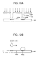
- FIGS. 4A to 4C there has been a spacer formation method suggested using an ink-jet device as shown in FIGS. 4A to 4C .
- an ink-jet device 50 is aligned to correspond to a formation position of the spacer 58 .
- ink from the ink-jet device 50 is jetted to the substrate 40 .
- the substrate 40 corresponds to at least one of the upper and lower plates of a LCD panel.
- the ink-jet device 50 jets ink using a thermal system or a piezoelectric system. Typically, the latter system is used.
- the ink-jet device 50 using the piezoelectric system consists of a vessel 52 for containing a material to be jetted, and an inkjet head 54 for jetting a material from the vessel 52 .
- the vessel 52 is filled with the spacer material 58
- the ink-jet head 54 is provided with a piezoelectric device and a nozzle 56 for jetting the spacer material 58 from the vessel 52 .
- a voltage is applied to the piezoelectric device, then a physical pressure is generated to cause a capillary phenomenon in which a flow path between the vessel 52 and the nozzle 56 repeatedly contracts and relaxes. Due to this capillary phenomenon, the spacer material 58 jets out of the nozzle 56 onto the substrate 40 , as shown in FIG. 4A .
- a curing process is used that exposes the spacer material 58 on the substrate 40 to an ultraviolet ray from a light source (not shown).
- the spacer material 58 can be hardened into a spacer 59 , as shown in FIG. 4B .
- the spacer material 58 has a hydrostatic property of being hydrophilic, the spacer 49 does not have good adhesion with the common electrode 14 that is also hydrophobic. Although the spacer may have a minimum height for keeping the cell gaps between the upper plate and the lower plate of the LCD panel, the lack of adhesion between the spacer and a plate of the LCD panel enables the spacers to move around.
- the present invention is directed to a liquid crystal display and a fabricating method thereof that obviates one or more of the problems due to limitations and disadvantages of the related art.
- An object of the present invention is to provide a liquid crystal display device and a fabricating method thereof wherein the adhesion of a spacer is increased to prevent a spacer from moving around within an LCD panel.
- an embodiment of the invention for a liquid crystal display includes an upper substrate, a lower substrate, a liquid crystal layer between the upper and lower substrates, a transparent electrode including of at least two layers of transparent material provided on at least one of the upper and lower substrates and a spacer material jetted onto the transparent electrode by an ink-jet system, wherein the spacer material has a hydrostatic property different from one of the at least two layers of the transparent electrode.
- a liquid crystal display device in another embodiment, includes an upper substrate, a lower substrate, a liquid crystal layer between the upper and lower substrates, a material layer with a surface that has a surface area with a first hydrostatic property and a spacer jetted onto the material layer by an ink-jet system and having a second hydrostatic property different from the first hydrostatic property.
- a liquid crystal display device in another embodiment, includes an upper substrate, a lower substrate, a liquid crystal layer between the upper and lower substrates, a material having a first hydrostatic property provided on at least one of the upper and lower substrates and a spacer between the upper and lower substrates having a second hydrostatic property different from the first hydrostatic property.
- a method of fabricating a liquid crystal display device includes the steps of forming a transparent electrode by depositing at least two transparent material layers on at least one of an upper and lower substrates, jetting a spacer material onto the transparent electrode by an ink-jet system, wherein the spacer material has a hydrostatic property different from one of the at least two layers of the transparent electrode, and providing a liquid crystal between the upper and lower substrates.
- a method of fabricating a liquid crystal display device includes the steps of treating a surface area of a material layer to change the hydrostatic property of the surface area, jetting a spacer material onto the surface area with an ink-jet system and providing a liquid crystal on the material layer.
- a method of fabricating a liquid crystal display device includes the steps of providing a material having a first hydrostatic property on a substrate, jetting a spacer material with a second hydrostatic property onto the material on the substrate with an ink-jet system; and providing a liquid crystal on the substrate.
- FIG. 1 is a cross-sectional view showing a structure of a conventional liquid crystal display.
- FIG. 2A to FIG. 2C are cross-sectional views representing a process of manufacturing a conventional pattern spacer.
- FIG. 3 is a flow chart representing the spacer manufacturing method shown in FIG. 2 .
- FIG. 4A and FIG. 4B depict a conventional spacer manufacturing method employing an ink-jet system.
- FIGS. 5A to 5C depict a method of fabricating a liquid crystal display employing an ink-jet system according to an embodiment of the present invention.
- FIG. 6A represents the contact angle of water to a hydrophobic surface of a single ITO layer of a conventional art device.
- FIG. 6B represents contact angle of water to a hydrophilic surface of multiple ITO layers in accordance with the present invention.
- FIGS. 7A to 7C depict a method of fabricating a liquid crystal display according to a second embodiment of the present invention.
- FIGS. 8A to 8C depict a method of fabricating a liquid crystal display according to a third embodiment of the present invention.
- FIGS. 9A to 9D depict a method of fabricating a liquid crystal display according to a fourth embodiment of the present invention.
- FIGS. 10A to 10B depict a method of fabricating a liquid crystal display according to a fifth embodiment of the present invention.
- FIGS. 11A to 11B depict a method of fabricating a liquid crystal display according to a sixth embodiment of the present invention.
- a liquid crystal display according to a first embodiment of the present invention includes a black matrix 74 provided on an upper substrate 70 to define a cell area, a color filter 72 provided on the cell area defined by the black matrix 74 , a common electrode 77 provided on the color filter 72 and made of a plurality of transparent electrode layers 77 , and a spacer 88 jetted on the top layer 76 of the multiple layer common electrode 77 with an ink-jet device 80 .
- the black matrix 74 defines a cell area in which the color filter 72 is formed, and prevents light leakage and absorbs external light to thereby enhance picture contrast.
- the color filter 72 is formed in the cell area defined by the black matrix 74 .
- the color filter 72 transmits a specific wavelength of light color, such as red, green or blue.
- the multiple layer common electrode 77 includes a plurality of transparent electrode layers, each of which is formed of, for example, indium-tin-oxide (ITO) that has good light transmittance and good conductivity.
- ITO indium-tin-oxide
- the top surface electrode layer 76 or upper layers of the multiple layer common electrode 77 have relativly less light transmittance and less conductivity than the lower layers. However, the top surface electrode layer 76 or upper layers have the hydrostatic property of being hydrophilic as opposed to the lower layers, which are hydrophobic.
- a black matrix 74 , a color filter 72 and a multiple layer common electrode 77 are provided on an upper substrate 70 .
- the O 2 gas input into the deposition process of the ITO is increased as each layer is deposited so that the top surface electrode layer has a hydrophilic property.
- the O 2 gas changes a hydrostatic property of the ITO material in that the ITO is changed form hydrophobic to hydrophilic as the O 2 gas concentration is increased.
- the resulting top layer 76 of the multiple layer common electrode 77 has a hydrophilic property.
- the hydrostatic property of the ITO material is changed without reducing the resistivity or transmittance of the multiple layer common electrode 77 significantly as a whole.
- the ink-jet device 80 includes a vessel 82 for containing the spacer material 88 to be jetted, and an ink-jet head 84 for jetting the spacer material from the vessel 82 .
- the vessel 82 is filled with the spacer material 88
- the ink-jet head 84 is provided with a piezoelectric device and a nozzle 86 for jetting the spacer material 88 contained in the vessel 82 .
- a hydrostatic property of the spacer material 88 is that it is hydrophobic. Since the spacer material 88 has a hydrophobic property and the top surface layer 76 of the multiple layer common transparent electrode 77 has a hydrophilic property, adhesion between the top transparent electrode layer 76 and the spacer material 88 increased. Thus, the subsequently cured spacer will not easily separate from the top transparent electrode layer 76 or move around.
- a conventional common electrode 78 that is a single layer
- a contact angle of water with respect to the ITO film is about 50°. Since the conventional common electrode 78 has a hydrophobic property while water has a hydrophilic property, a contact angle is large.
- a contact angle of water with respect to the top surface common electrode layer 76 becomes about 27°. This is because the top surface common electrode layer 76 has a hydrophilic property as a result of increasing the O 2 gas injection into the deposition process for each ITO layer as each layer is deposited until the top surface electrode layer has a hydrophilic property. Since the top surface electrode layer 76 is hydrophilic, the multiple layered common electrode 77 attracts or mixes well with water.
- FIGS. 7A to 7C show a method of fabricating a liquid crystal display according to a second embodiment of the present invention.
- a film 94 having a hydrophobic surface is provided on a substrate 92 .
- the substrate can be the upper plate or lower plate of an LCD panel.
- the film 94 can be an ITO film.
- the film 94 can be an organic film or inorganic film, for example, silicon nitride (SiN x ) used on portions of an ITO film or in lieu of the ITO film to create surface areas having a hydrophobic surface.
- the film 94 can be an inorganic or organic film on portions of the lower plate of an LCD in which the pixel electrode is not present.
- the surface of the film 94 is subjected to an O 2 or H 2 plasma treatment, thereby changing the hydrostatic property of the surface of film 94 from a hydrophobic property to a hydrophilic property.
- the surface of the film 94 can be changed to have a hydrophilic property by utilizing an acid solution treatment, a basic solution treatment, an ion beam treatment or an ultraviolet ray treatment instead of the O 2 or H 2 plasma treatment.
- an ink-jet device 80 is aligned to a black matrix (not shown) under the ITO film of the upper plate of an LCD panel or to an area of the lower plate of an LCD panel in which the pixel electrode is not present.
- the spacer material 90 is jetted onto the film 94 . If the spacer material 90 has a hydrophobic property and is jetted onto the film 94 having a surface with a hydrophilic property, then the contact angle between the film 94 and the spacer material 90 will be increased, as shown in FIG. 7C . The increased contact angle increases the height of the spacer while minimally increasing the width of the spacer for obtaining a specified cell gap with increased aperture.
- a solvent within the spacer material 90 is evaporated through a curing process to harden the spacer material 90 into a spacer.
- FIGS. 8A to 8C show a method of fabricating a liquid crystal display according to a third embodiment of the present invention.
- a material 122 having a hydrophilic property is coated onto a substrate 120 .
- an ink-jet device can be used to coat the substrate 120 with the material 122 for good adhesion.
- the substrate 120 can be an upper plate or a lower plate of the liquid crystal display panel.
- an ink-jet device 126 is aligned on the substrate at a position on which a spacer is to be formed. Then, a spacer material 124 is jetted onto the substrate 120 .
- the spacer material 124 has a hydrostatic property of being hydrophobic.
- FIGS. 9A to 9D show a method of fabricating a liquid crystal display according to a fourth embodiment of the present invention.
- an ink-jet device 134 is aligned on a substrate 130 to drop a hydrophilic material 132 in correspondence with a spacer area.
- the substrate 130 may be an upper plate or a lower plate of the liquid crystal display panel.
- the hydrophilic material 132 jetted from the ink-jet device 134 is formed to be spread somewhat widely on the substrate 130 for good adhesion, as shown in FIG. 9B .
- the ink-jet device 134 in which a hydrophobic spacer material 136 is contained is aligned to jet the hydrophobic spacer material 136 onto said hydrophilic material 132 , as shown in FIG. 9C .
- the hydrophobic spacer material 136 does not necessarily need to undergo a curing process. Because the spacer material 136 is a hydrophobic material having a property repulsing from the hydrophilic material 132 , it can be formed at a larger height or with a greater contact angle than in the related art. In other words, the hydrophobic spacer material 136 is positioned upon the hydrophilic material 132 as shown in FIG.
- a formation height of the spacer 136 can be set to a desired suitable height for the cell gap.
- a formation height of the spacer 136 can be approximately 3 to 5 ⁇ m.
- FIG. 10A and FIG. 10B show a method of fabricating a liquid crystal display according to a fifth embodiment of the present invention.
- an ultraviolet ray or an ion beam is radiated on, or a plasma treatment is performed on the surface of a material layer 100 corresponding to a surface area 100 a at which a spacer is to be formed.
- a ratio of a height of the spacer extending from the upper plate to a width of the spacer on the upper plate should be sufficiently large to maintain the aperture and contrast of the LCD panel.
- the contact angle should be large. However, if a contact angle between the spacer material and the surface of the substrate 100 is too large, then the spacer may be easily separated from the substrate 100 even though the spacer is formed on the substrate 100 .
- an ultraviolet ray is selectively radiated only on a surface area 100 a to change the hydrostatic property of a surface of the material layer 100 where a spacer will be positioned, thereby enhancing an adhesive force while increasing the contact angle between the material layer 100 and the spacer.
- a mask 102 having light transmitting parts 102 a and light shielding parts 102 b arranged alternately is aligned to the material layer 100 .
- the light transmitting part 102 a of the mask 102 corresponds to a surface area 100 a at which a spacer is to be formed while the light shielding part 102 b corresponds to peripheral material layer area 100 b on which a spacer will not be formed.
- an ultraviolet ray or an ion beam is radiated such that the ultraviolet ray or an ion beam passes through the light transmitting part 102 a and changes a property of the surface area 100 a of the surface of the material layer 100 to thereby enhance an adhesive force between the spacer and the material layer 100 .
- an area 100 b in which an ultraviolet ray is not radiated has a hydrostatic property that repulses the spacer material.
- the surface property can be changed by a plasma treatment instead of a light treatment.
- a surface area 100 a of the material layer on which spacers will be formed is changed from a hydrophobic property to a hydrophilic property by the surface area treatment.
- a surface area 100 a of the material layer 100 has a different hydrostatic property from the peripheral material layer areas 100 b corresponding to a surface of the material layer 100 other than on which a spacer will be formed.
- a hydrophilic spacer material 106 is jetted onto the surface areas 100 a through a nozzle of the ink-jet device. Since the hydrophilic spacer material 106 has a hydrostatic property different than the peripheral material layer area 100 b , the spacer material 106 has a large contact angle due to the difference of hydrostatic properties between the peripheral material layer area 100 b and the spacer material. In addition, the hydrophilic spacer material 106 has good adhesion due to the substrate 100 a and the spacer material 106 having the same hydrostatic property.
- FIGS. 11A and 11B show a method of fabricating a liquid crystal display according to a sixth embodiment of the present invention.
- an ultraviolet ray or an ion beam is radiated on or a plasma treatment is performed on peripheral material layer areas 116 b other than surface areas 116 a at which spacers are to be formed.
- the contact angle should be large. However, if a contact angle between the spacer material and the surface of the material layer 116 is too large, the spacer may be easily separated from the material layer 116 .
- an ultraviolet ray is selectively radiated only on peripheral material layer area 116 b other than surface areas 116 a at which spacer are to be formed, thereby enhancing an adhesive force while increasing the contact angle between the material layer 116 and the spacer.
- a mask 110 having a light shielding part 110 a and a light transmitting part 110 b arranged alternately is aligned to the material layer 116 .
- the light transmitting part 110 b of the mask 110 corresponds to an peripheral material layer area 116 b other than a surface area at which the spacer is to be formed while the light shielding part 110 a corresponds to a surface area 116 a at which the spacer is to be formed.
- an ultraviolet ray or an ion beam is radiated.
- the ultraviolet ray or ion beam passing through the light transmitting part 110 b changes a surface property of said peripheral material layer area 116 b , thereby changing the surface of the material layer 116 to have a large contact angle.
- the surface property can be changed by a plasma treatment instead of a light or ion beam treatment.
- the surface area 116 a onto which the ultraviolet ray is not radiated has an advantage in that an adhesive force is increased between the spacer and the material layer 116 .
- the surface area 116 a of the surface on material layer 116 has a hydrostatic property different from the peripheral material layer area 116 b.
- a hydrophilic spacer material 112 is jetted onto the surface area 116 a by means of the ink-jet device 104 . Since the surface area 116 a and the peripheral material layer area 116 b have a different surface property from each other, a spacer material 112 jetted from the ink-jet device 104 is formed only at the spacer formation area 116 a . Thus, the hydrophilic spacer material 112 is formed to be higher than the related art, so that the height of the spacer 11 2 increases relative to its width. Therefore, the spacer material 112 has good adhesion to the material layer 116 . Accordingly, it becomes possible to easily make the spacer 112 corresponding to a desired suitable height for a cell gap in an LCD panel.
- a hydrostatic property of the substrate on which the spacer is formed is made different from that of the spacer material. Accordingly, the spacer can be formed with good adhesion, is formed at a large height owing to a repulsion force between the substrate and the spacer. In other words, it is possible to more easily obtain a height for a spacer having good adhesion to a substrate for maintaining cell gap while also maintaining aperture size for the cells of a LCD panel.
Landscapes
- Physics & Mathematics (AREA)
- Nonlinear Science (AREA)
- Mathematical Physics (AREA)
- Chemical & Material Sciences (AREA)
- Crystallography & Structural Chemistry (AREA)
- General Physics & Mathematics (AREA)
- Optics & Photonics (AREA)
- Liquid Crystal (AREA)
Abstract
Description
Claims (15)
Applications Claiming Priority (2)
| Application Number | Priority Date | Filing Date | Title |
|---|---|---|---|
| KR10-2002-0027182A KR100475164B1 (en) | 2002-05-16 | 2002-05-16 | Liquid Crystal Display and Method of Fabricating the same |
| KRP2002-27182 | 2002-05-16 |
Publications (2)
| Publication Number | Publication Date |
|---|---|
| US20030214620A1 US20030214620A1 (en) | 2003-11-20 |
| US7102722B2 true US7102722B2 (en) | 2006-09-05 |
Family
ID=29417397
Family Applications (1)
| Application Number | Title | Priority Date | Filing Date |
|---|---|---|---|
| US10/266,740 Expired - Fee Related US7102722B2 (en) | 2002-05-16 | 2002-10-09 | Liquid crystal display and a fabricating method thereof |
Country Status (2)
| Country | Link |
|---|---|
| US (1) | US7102722B2 (en) |
| KR (1) | KR100475164B1 (en) |
Cited By (6)
| Publication number | Priority date | Publication date | Assignee | Title |
|---|---|---|---|---|
| US20040125324A1 (en) * | 2001-12-24 | 2004-07-01 | Kim Jeong Hyun | Method of fabricating liquid crystal display device |
| US20050043186A1 (en) * | 2003-04-25 | 2005-02-24 | Semiconductor Energy Laboratory Co., Ltd. | Method for forming pattern and drop discharge apparatus |
| US20050140890A1 (en) * | 2003-12-30 | 2005-06-30 | Lg.Philips Lcd Co., Ltd. | Thin film transistor device, liquid crystal display device using the same, and method of fabricating the same |
| US20070066022A1 (en) * | 2005-09-22 | 2007-03-22 | Neng-Kuo Chen | Method of fabricating silicon nitride layer and method of fabricating semiconductor device |
| US20070285609A1 (en) * | 2004-10-19 | 2007-12-13 | Yasuzo Tanaka | Spacer Forming Method and Spacer Forming Apparatus |
| US9335589B2 (en) | 2014-01-10 | 2016-05-10 | Samsung Display Co., Ltd. | Display apparatus and method of manufacturing the same |
Families Citing this family (14)
| Publication number | Priority date | Publication date | Assignee | Title |
|---|---|---|---|---|
| KR100956939B1 (en) * | 2003-06-19 | 2010-05-11 | 엘지디스플레이 주식회사 | LCD panel and manufacturing method |
| KR101039450B1 (en) * | 2003-06-19 | 2011-06-07 | 엘지디스플레이 주식회사 | LCD panel, manufacturing method and apparatus thereof |
| JP3994994B2 (en) * | 2003-10-23 | 2007-10-24 | セイコーエプソン株式会社 | Organic EL device manufacturing method, organic EL device, and electronic apparatus |
| SE0303604L (en) * | 2003-12-30 | 2005-11-18 | Swedish Lcd Ct Ab | A process for manufacturing LCD |
| US7400374B2 (en) * | 2004-05-28 | 2008-07-15 | Kyocera Corporation | Liquid crystal display device having black and transparent spacers in the transmissive region |
| TW200628938A (en) * | 2005-02-02 | 2006-08-16 | Quanta Display Inc | Substrate of a liquid crystal display and method of forming an alignment layer |
| KR101091743B1 (en) * | 2005-02-23 | 2011-12-08 | 엘지디스플레이 주식회사 | Method for forming spacer using ink-jet dropping method |
| US7601567B2 (en) * | 2005-12-13 | 2009-10-13 | Samsung Mobile Display Co., Ltd. | Method of preparing organic thin film transistor, organic thin film transistor, and organic light-emitting display device including the organic thin film transistor |
| KR101350250B1 (en) * | 2007-09-05 | 2014-01-10 | 히타치가세이가부시끼가이샤 | Process for producing spacer for liquid crystal display apparatus, ink for spacer formation, liquid crystal display apparatus and process for manufacturing the same |
| KR20140065271A (en) * | 2012-11-21 | 2014-05-29 | 삼성디스플레이 주식회사 | Liquid crystal display and manufacturing method thereof |
| CN106229425B (en) * | 2016-09-09 | 2018-05-18 | 广州新视界光电科技有限公司 | A kind of full-color organic light emitting display of top emitting and preparation method |
| CN107369777B (en) * | 2017-08-31 | 2020-01-03 | 京东方科技集团股份有限公司 | OLED substrate, preparation method thereof and display device |
| CN107505766B (en) * | 2017-10-12 | 2020-05-05 | 深圳市华星光电半导体显示技术有限公司 | Color film substrate, manufacturing method thereof and structure for increasing thickness of film layer |
| US20190139823A1 (en) * | 2017-11-06 | 2019-05-09 | Globalfoundries Inc. | Methods of forming conductive lines and vias and the resulting structures |
Citations (7)
| Publication number | Priority date | Publication date | Assignee | Title |
|---|---|---|---|---|
| JPH03246521A (en) * | 1990-02-23 | 1991-11-01 | Kao Corp | Production of spacer for liquid crystal display |
| JPH06324357A (en) * | 1993-05-12 | 1994-11-25 | Toshiba Corp | Liquid crystal display element |
| US5739882A (en) * | 1991-11-18 | 1998-04-14 | Semiconductor Energy Laboratory Co., Ltd. | LCD polymerized column spacer formed on a modified substrate, from an acrylic resin, on a surface having hydrophilic and hydrophobic portions, or at regular spacings |
| JP2001083314A (en) | 1999-09-09 | 2001-03-30 | Canon Inc | Color filter with spacer, its manufacture and liquid crystal element utilizing the same |
| US6441880B1 (en) * | 1998-01-30 | 2002-08-27 | Hitachi, Ltd. | Normally closed liquid crystal display device using spacers coated with material having liquid crystal aligning ability by irradiation with polarized light |
| US6501527B1 (en) * | 1999-07-29 | 2002-12-31 | Canon Kabushiki Kaisha | Liquid crystal elemental device, production process thereof and spacer-bearing substrate |
| US6812990B1 (en) * | 2000-04-26 | 2004-11-02 | Micron Technology, Inc. | Method for making sol gel spacers for flat panel displays |
Family Cites Families (5)
| Publication number | Priority date | Publication date | Assignee | Title |
|---|---|---|---|---|
| JP2001109002A (en) * | 1999-10-07 | 2001-04-20 | Canon Inc | Color filter with spacer, its production and liquid crystal device using that color filter |
| JP2001083528A (en) * | 1999-09-13 | 2001-03-30 | Canon Inc | Liquid crystal device, its production, substrate with spacer and its production |
| JP2001083525A (en) * | 1999-09-09 | 2001-03-30 | Canon Inc | Color filter with spacer, its production and liquid crystal device using that color filter |
| JP4365489B2 (en) * | 1999-09-20 | 2009-11-18 | 大日本印刷株式会社 | Color filter and manufacturing method thereof |
| JP2001109004A (en) * | 1999-10-07 | 2001-04-20 | Canon Inc | Color filter with spacer, its production and liquid crystal device using that color filter |
-
2002
- 2002-05-16 KR KR10-2002-0027182A patent/KR100475164B1/en active IP Right Grant
- 2002-10-09 US US10/266,740 patent/US7102722B2/en not_active Expired - Fee Related
Patent Citations (7)
| Publication number | Priority date | Publication date | Assignee | Title |
|---|---|---|---|---|
| JPH03246521A (en) * | 1990-02-23 | 1991-11-01 | Kao Corp | Production of spacer for liquid crystal display |
| US5739882A (en) * | 1991-11-18 | 1998-04-14 | Semiconductor Energy Laboratory Co., Ltd. | LCD polymerized column spacer formed on a modified substrate, from an acrylic resin, on a surface having hydrophilic and hydrophobic portions, or at regular spacings |
| JPH06324357A (en) * | 1993-05-12 | 1994-11-25 | Toshiba Corp | Liquid crystal display element |
| US6441880B1 (en) * | 1998-01-30 | 2002-08-27 | Hitachi, Ltd. | Normally closed liquid crystal display device using spacers coated with material having liquid crystal aligning ability by irradiation with polarized light |
| US6501527B1 (en) * | 1999-07-29 | 2002-12-31 | Canon Kabushiki Kaisha | Liquid crystal elemental device, production process thereof and spacer-bearing substrate |
| JP2001083314A (en) | 1999-09-09 | 2001-03-30 | Canon Inc | Color filter with spacer, its manufacture and liquid crystal element utilizing the same |
| US6812990B1 (en) * | 2000-04-26 | 2004-11-02 | Micron Technology, Inc. | Method for making sol gel spacers for flat panel displays |
Cited By (12)
| Publication number | Priority date | Publication date | Assignee | Title |
|---|---|---|---|---|
| US20040125324A1 (en) * | 2001-12-24 | 2004-07-01 | Kim Jeong Hyun | Method of fabricating liquid crystal display device |
| US7812915B2 (en) * | 2001-12-24 | 2010-10-12 | Lg. Display Co., Ltd. | Method of fabricating liquid crystal display device |
| US20050043186A1 (en) * | 2003-04-25 | 2005-02-24 | Semiconductor Energy Laboratory Co., Ltd. | Method for forming pattern and drop discharge apparatus |
| US20050140890A1 (en) * | 2003-12-30 | 2005-06-30 | Lg.Philips Lcd Co., Ltd. | Thin film transistor device, liquid crystal display device using the same, and method of fabricating the same |
| US7489368B2 (en) * | 2003-12-30 | 2009-02-10 | Lg Display Co., Ltd. | Thin film transistor device, liquid crystal display device using the same, and method of fabricating the same |
| US20090128728A1 (en) * | 2003-12-30 | 2009-05-21 | Jong Il Kim | Thin film transistor device, liquid crystal display device using the same, and method of fabricating the same |
| US8081266B2 (en) | 2003-12-30 | 2011-12-20 | Lg Display Co., Ltd. | Thin film transistor device, liquid crystal display device using the same, and method of fabricating the same |
| US20070285609A1 (en) * | 2004-10-19 | 2007-12-13 | Yasuzo Tanaka | Spacer Forming Method and Spacer Forming Apparatus |
| US7671962B2 (en) * | 2004-10-19 | 2010-03-02 | Ulvac, Inc. | Spacer forming method and spacer forming apparatus |
| US20070066022A1 (en) * | 2005-09-22 | 2007-03-22 | Neng-Kuo Chen | Method of fabricating silicon nitride layer and method of fabricating semiconductor device |
| US7544603B2 (en) * | 2005-09-22 | 2009-06-09 | United Microelectronics Corp. | Method of fabricating silicon nitride layer and method of fabricating semiconductor device |
| US9335589B2 (en) | 2014-01-10 | 2016-05-10 | Samsung Display Co., Ltd. | Display apparatus and method of manufacturing the same |
Also Published As
| Publication number | Publication date |
|---|---|
| KR100475164B1 (en) | 2005-03-08 |
| US20030214620A1 (en) | 2003-11-20 |
| KR20030089131A (en) | 2003-11-21 |
Similar Documents
| Publication | Publication Date | Title |
|---|---|---|
| US7102722B2 (en) | Liquid crystal display and a fabricating method thereof | |
| US7369207B2 (en) | Liquid crystal display with spacer positioned within a hole of a pixel electrode and a fabricating method thereof | |
| US7362405B2 (en) | Method of fabricating liquid crystal display device | |
| TWI354845B (en) | Liquid crystal display panel having a constant cel | |
| JP2009104182A (en) | Thin film patterning apparatus and method of fabricating color filter array substrate using the same | |
| US20030076457A1 (en) | Color filter substrate for liquid crystal display and manufacturing method thereof | |
| US7760321B2 (en) | Method of manufacturing a liquid crystal display device | |
| US20110211147A1 (en) | Liquid crystal display panel and fabricating method and apparatus thereof | |
| US7248312B2 (en) | Liquid crystal display panel and fabricating method thereof | |
| CN101149506B (en) | Method for manufacturing liquid crystal display panel and liquid crystal display panel | |
| US7338556B2 (en) | Apparatus and method for fabricating a liquid crystal display | |
| US7727577B2 (en) | Apparatus and method for fabricating a liquid crystal display panel | |
| KR20070069829A (en) | LCD and its manufacturing method | |
| KR20030057146A (en) | A color filter and An array substrate for LCD and method for fabricating the same | |
| KR100939209B1 (en) | LCD and its manufacturing method | |
| KR20040051951A (en) | Liquid Crystal Display Panel And Fabricating Method Thereof | |
| KR100886229B1 (en) | LCD and its manufacturing method | |
| KR20040018674A (en) | Liquid Crystal Display and Method of Fabricating the same | |
| KR100908657B1 (en) | LCD panel and manufacturing method | |
| KR20170045618A (en) | Liquid crystal display device having uniform alignment layer | |
| KR20040024364A (en) | Liquid crystal display and method of fabricating the same | |
| KR20040040636A (en) | Liquid Crystal Display Panel And Fabricating Method Thereof | |
| KR20040024110A (en) | Method of fabricating liquid crystal display | |
| KR20040031364A (en) | Liquid Crystal Display and Method of Fabricating the same | |
| KR20030047022A (en) | A method for fabricating color filter substrate for LCD |
Legal Events
| Date | Code | Title | Description |
|---|---|---|---|
| AS | Assignment |
Owner name: L.G. PHILIPS LCD CO., LTD., KOREA, REPUBLIC OF Free format text: ASSIGNMENT OF ASSIGNORS INTEREST;ASSIGNORS:KIM, JEONG HYUN;JUN, JAE HONG;LEE, HYUN KYU;AND OTHERS;REEL/FRAME:013377/0688 Effective date: 20020925 |
|
| AS | Assignment |
Owner name: LG DISPLAY CO., LTD., KOREA, REPUBLIC OF Free format text: CHANGE OF NAME;ASSIGNOR:LG.PHILIPS LCD CO., LTD.;REEL/FRAME:021147/0009 Effective date: 20080319 Owner name: LG DISPLAY CO., LTD.,KOREA, REPUBLIC OF Free format text: CHANGE OF NAME;ASSIGNOR:LG.PHILIPS LCD CO., LTD.;REEL/FRAME:021147/0009 Effective date: 20080319 |
|
| FEPP | Fee payment procedure |
Free format text: PAYER NUMBER DE-ASSIGNED (ORIGINAL EVENT CODE: RMPN); ENTITY STATUS OF PATENT OWNER: LARGE ENTITY Free format text: PAYOR NUMBER ASSIGNED (ORIGINAL EVENT CODE: ASPN); ENTITY STATUS OF PATENT OWNER: LARGE ENTITY |
|
| FPAY | Fee payment |
Year of fee payment: 4 |
|
| FPAY | Fee payment |
Year of fee payment: 8 |
|
| FEPP | Fee payment procedure |
Free format text: MAINTENANCE FEE REMINDER MAILED (ORIGINAL EVENT CODE: REM.) |
|
| LAPS | Lapse for failure to pay maintenance fees |
Free format text: PATENT EXPIRED FOR FAILURE TO PAY MAINTENANCE FEES (ORIGINAL EVENT CODE: EXP.); ENTITY STATUS OF PATENT OWNER: LARGE ENTITY |
|
| STCH | Information on status: patent discontinuation |
Free format text: PATENT EXPIRED DUE TO NONPAYMENT OF MAINTENANCE FEES UNDER 37 CFR 1.362 |
|
| FP | Lapsed due to failure to pay maintenance fee |
Effective date: 20180905 |