US7026199B2 - Transistor of semiconductor device and method for manufacturing the same - Google Patents
Transistor of semiconductor device and method for manufacturing the same Download PDFInfo
- Publication number
- US7026199B2 US7026199B2 US10/878,328 US87832804A US7026199B2 US 7026199 B2 US7026199 B2 US 7026199B2 US 87832804 A US87832804 A US 87832804A US 7026199 B2 US7026199 B2 US 7026199B2
- Authority
- US
- United States
- Prior art keywords
- film
- oxide film
- forming
- nitride film
- pad
- Prior art date
- Legal status (The legal status is an assumption and is not a legal conclusion. Google has not performed a legal analysis and makes no representation as to the accuracy of the status listed.)
- Expired - Fee Related
Links
Images


Classifications
-
- H—ELECTRICITY
- H01—ELECTRIC ELEMENTS
- H01L—SEMICONDUCTOR DEVICES NOT COVERED BY CLASS H10
- H01L21/00—Processes or apparatus adapted for the manufacture or treatment of semiconductor or solid state devices or of parts thereof
- H01L21/02—Manufacture or treatment of semiconductor devices or of parts thereof
- H01L21/04—Manufacture or treatment of semiconductor devices or of parts thereof the devices having potential barriers, e.g. a PN junction, depletion layer or carrier concentration layer
- H01L21/18—Manufacture or treatment of semiconductor devices or of parts thereof the devices having potential barriers, e.g. a PN junction, depletion layer or carrier concentration layer the devices having semiconductor bodies comprising elements of Group IV of the Periodic Table or AIIIBV compounds with or without impurities, e.g. doping materials
-
- H—ELECTRICITY
- H10—SEMICONDUCTOR DEVICES; ELECTRIC SOLID-STATE DEVICES NOT OTHERWISE PROVIDED FOR
- H10D—INORGANIC ELECTRIC SEMICONDUCTOR DEVICES
- H10D30/00—Field-effect transistors [FET]
- H10D30/60—Insulated-gate field-effect transistors [IGFET]
- H10D30/62—Fin field-effect transistors [FinFET]
- H10D30/6211—Fin field-effect transistors [FinFET] having fin-shaped semiconductor bodies integral with the bulk semiconductor substrates
-
- H—ELECTRICITY
- H10—SEMICONDUCTOR DEVICES; ELECTRIC SOLID-STATE DEVICES NOT OTHERWISE PROVIDED FOR
- H10D—INORGANIC ELECTRIC SEMICONDUCTOR DEVICES
- H10D30/00—Field-effect transistors [FET]
- H10D30/01—Manufacture or treatment
- H10D30/021—Manufacture or treatment of FETs having insulated gates [IGFET]
- H10D30/024—Manufacture or treatment of FETs having insulated gates [IGFET] of fin field-effect transistors [FinFET]
-
- H—ELECTRICITY
- H10—SEMICONDUCTOR DEVICES; ELECTRIC SOLID-STATE DEVICES NOT OTHERWISE PROVIDED FOR
- H10D—INORGANIC ELECTRIC SEMICONDUCTOR DEVICES
- H10D30/00—Field-effect transistors [FET]
- H10D30/60—Insulated-gate field-effect transistors [IGFET]
- H10D30/62—Fin field-effect transistors [FinFET]
- H10D30/6219—Fin field-effect transistors [FinFET] characterised by the source or drain electrodes
Definitions
- the present invention relates to transistor of semiconductor device and method for manufacturing the same, and in particular to an improved transistor of semiconductor device and method for manufacturing the same wherein a channel region is formed on a sidewall of a: silicon fin extruding above a device isolation region and the contact area is expanded to the sidewall at the end of the silicon fin to prevent short channel effect and provide an increased current driving capability and reduced contact resistance.
- a DRAM comprises a transistor and a capacitor. As a design rule of the transistor is reduced, a channel length of the cell transistor is also decreased.
- a short channel effect occurs due to a decrease in the channel length of the transistor, thereby degrading the characteristic of the transistor.
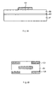
- FIG. 1 is a layout view illustrating a conventional semiconductor device.
- ends of an active region 200 is immediately adjacent to a gate region 400 .
- FIGS. 2A through 2H are cross-sectional views illustrating a conventional method for manufacturing a transistor of semiconductor device, wherein FIGS. 2A through 2G are cross-sectional views taken along the line A—A of FIG. 1 and FIG. 2H is a cross-sectional view taken along the line B—B of FIG. 2G .
- a well (not shown) is formed on a semiconductor substrate 11 . Thereafter, a pad oxide film 13 and a pad nitride film 15 are sequentially formed on the semiconductor substrate 11 .
- the pad nitride film 15 , the pad oxide film 13 and a predetermined thickness of the semiconductor substrate 11 are etched via photolithography process using a device isolation mask (not shown) to form a trench 21 .
- a thermal oxide film 17 is formed on a surface of the trench 21 and a liner nitride film 19 is then formed on the entire surface of the semiconductor substrate 11 including the trench 21 .
- an oxide film (not shown) at least filling the trench 21 is formed on the entire surface of the semiconductor substrate 11 and then planarized via a CMP process until the pad nitride film 15 is exposed to form a device isolation film 23 .
- the pad nitride film 15 and the liner nitride film 19 exposed by the device isolation film 23 are removed by a wet-etch process using a H 3 PO 4 solution.
- the pad oxide film 13 is removed by a wet-etch process and a gate oxide film 25 is formed on the semiconductor substrate 11 .
- a polysilicon layer 27 for gate electrode, a barrier metal layer 29 comprising tungsten nitride, a metal layer 31 comprising tungsten, a hard mask nitride film 33 are sequentially formed on the gate oxide film 25 .
- the hard mask nitride film 33 , the metal layer 31 , the barrier metal layer 29 and the polysilicon layer 27 are etched via a photolithography process using a gate electrode mask (not shown) to form a gate electrode.
- an oxide film 35 is formed on a sidewall of the polysilicon layer 27 .
- a nitride film 37 having a predetermined thickness is formed on the entire surface of the semiconductor substrate 11 including the gate electrode. Thereafter, a lower insulating film 39 is formed and etched back until the nitride film 37 is exposed.
- the lower insulating film 39 and the nitride film 37 are anisotropically etched via a photolithography process using a landing plug contact hole mask to form a nitride spacer and a landing plug contact hole 41 .
- an impurity is ion-implanted in the semiconductor substrate 11 at the bottom of the landing plug contact hole 41 to form a source/drain region 44 .
- a polysilicon film for landing plug (not shown) filling the landing plug contact hole 41 is formed on the entire surface of the semiconductor substrate 11 and then planarized until the hard mask nitride film 33 is exposed to form a landing plug 43 .
- the channel length is decreased, resulting in short channel effect.
- a method of increasing impurity concentration of the channel region has been proposed.
- an increase in the impurity concentration results in increase in electric field and leakage current, which deteriorate refresh time characteristic of the device.
- the reduction of the design rule also decrease the contact area between the source/drain region of the cell transistor and the landing plug, resulting in increase in contact resistance.
- FIGS. 3 is a layout view illustrating another conventional semiconductor device, wherein a fin type field effect transistor formed on a SOI (Silicon-On-Insulator) wafer is shown.
- SOI Silicon-On-Insulator
- a silicon fin region 600 connecting source/drain regions 500 is used as a channel and a gate electrode region 700 is disposed on the silicon fin region 600 .
- FIGS. 4A through 4F are cross-sectional views illustrating another conventional method for manufacturing a transistor of semiconductor device shown in FIG. 3 , wherein FIGS. 4A through 4E are cross-sectional views taken along the line A—A of FIG. 3 and FIG. 4F is a cross-sectional view taken along the line B—B of FIG. 3 .
- a first nitride film (not shown) and a first oxide film (not shown) are sequentially formed on a SOI wafer including a stacked structure of a buried oxide film 53 and a silicon body 55 .
- the first oxide film and the first nitride film are patterned to form a first oxide film pattern 59 and a first nitride film pattern 57 .
- the silicon body 55 is etched using the first oxide film pattern 59 as an etching mask to form a silicon fin 61 .
- the silicon fin 61 serves as a channel of the transistor.
- a polysilicon film 63 and a second oxide film 65 are sequentially formed on the entire surface of the SOI wafer.
- the polysilicon film 63 is used as a source/drain region of the transistor.
- the second oxide film 65 and the polysilicon film 63 are patterned to form a recess 69 defining a gate region.
- a third oxide film (not shown) is deposited on the entire surface and then anisotropically etched to form an oxide film spacer 67 on a sidewall of the recess 69 .
- the anisotropic etching process is an over-etch process wherein the first oxide film pattern 59 and the first nitride film pattern 57 exposed by the oxide film spacer 67 are etched to expose the silicon fin 61 and a predetermined thickness of the buried oxide film 53 is additionally etched.
- a gate oxide film 71 is formed on the exposed portion of the silicon fin 61 and a gate electrode 73 is then formed by filling the recess 69 using a polycrystalline SiGe layer.
- the short channel effect can be reduced.
- the production cost of the device is increased due to the use of SOI wafer.
- the refresh characteristic of the device is deteriorated.
- a method for manufacturing the transistor of semiconductor device comprising the steps of: (a) forming a trench type device isolation film defining a I-type active region on a semiconductor substrate having a stacked structure of a pad oxide film, a pad nitride film thereon; (b) etching a predetermined thickness of the device isolation film to form a silicon fin extruding above the device isolation film; (c) tilt implanting an impurity on a sidewall of the silicon fin to form a channel region; (d) forming a gate oxide film on the sidewall of the silicon fin; (e) forming a planarized polysilicon layer for gate electrode on the semiconductor substrate; (f) patterning the polysilicon layer and the pad nitride film to form a gate electrode; (g) forming a lower insulating film including a landing plug contact hole exposing a portion of the pad oxide film and a portion of the gate oxide film; (h) performing an i
- a transistor of semiconductor device comprising: an I-type active region defined by a trench type device isolation film, wherein the I-type active region includes a silicon fin extrudes above the trench type device isolation film; a gate oxide film disposed on a sidewall of the silicon fin; a set of gate electrodes having a planarized top surface, wherein the gate electrode extends across and perpendicular to the I-type active region; a pad insulating film disposed at an interface of an upper surface of the silicon fin and a lower surface of the gate electrode; a source/drain region disposed on the silicon fin between the gate electrodes and at both sides of the gate electrode; a channel region disposed at the sidewall of the silicon fin under the gate oxide film and between the gate electrodes.
- FIG. 1 is a layout view illustrating a conventional semiconductor device.
- FIGS. 2A through 2H are cross-sectional views illustrating a conventional method for manufacturing a transistor of semiconductor device.
- FIG. 3 is a layout view illustrating another conventional semiconductor device.
- FIGS. 4A through 4F are cross-sectional views illustrating another conventional method for manufacturing a transistor of semiconductor device shown in FIG. 3 .
- FIGS. 5 is a layout view illustrating a semiconductor device in accordance with the present invention.
- FIG. 6 is a perspective view illustrating a transistor of semiconductor device in accordance with a first preferred embodiment of the present invention.
- FIGS. 7A through 7H are cross-sectional views illustrating method for manufacturing transistor of semiconductor device in accordance with the first preferred embodiment of the present invention.
- FIGS. 8A and 8B are a cross-sectional view and a plane view respectively, illustrating a method for manufacturing an active region having a shorter length than a conventional one in accordance with a second preferred embodiment of the present invention.
- FIG. 9 is a cross-sectional diagram illustrating a method for manufacturing an active region having a shorter length than a conventional one in accordance with a third preferred embodiment of the present invention.
- FIG. 5 is a layout view illustrating a semiconductor device in accordance with the present invention.
- the semiconductor device comprises a device isolation region 900 for defining an active region 800 .
- the active region 800 comprises a contact region 1100 including a source/drain region, and an end portion of the active region 800 in its lengthwise direction is spaced apart from a gate region 1000 .
- the space between active region 800 and the gate region 1000 prevents short between a gate electrode formed in the gate region 1000 and the active region 800 including a silicon fin extruding above the device isolation region 900 .
- a contact area of a landing plug is increased to improve contact characteristic because the landing plug contacts a sidewall of the extruding silicon fin of the active region 800 .
- FIG. 6 is a perspective view illustrating a transistor of semiconductor device in accordance with an embodiment of the present invention, wherein an enlarged view of region ‘a’ in FIG. 5 is illustrated.
- FIG. 6 Only a silicon fin 82 of the active region formed in a semiconductor substrate 81 , a channel region 97 , a source/drain region 123 , a pad insulating film 83 and 85 and a gate electrode 110 are shown in FIG. 6 for simplicity.
- FIG. 7G A detailed cross-sectional view of the transistor of semiconductor device in accordance with the present invention is shown in FIG. 7G .
- the semiconductor device shown in FIG. 6 comprises a semiconductor substrate 81 and an I-type active region including a silicon fin 82 .
- the I-type active region is defined by a trench type device isolation film.
- the silicon fin 82 extrudes above the trench type device isolation film and is spaced apart from adjacent gate electrodes.
- a set of gate electrodes 110 having a planarized top surface is disposed so that the gate electrodes 110 extend across and perpendicular to the silicon fin 82 .
- a gate oxide film (not shown) is disposed on a sidewall of the silicon fin 82 , and a channel region 97 is disposed at the sidewall of the silicon fin 82 under the gate oxide film and between the set gate electrodes 110 . Because the gate electrodes 110 contact an upper surface and the sidewall of the silicon fin 82 , the width of the channel region 97 is two times the height of the silicon fin 82 .
- the semiconductor device comprises a pad insulating film disposed at an interface of an upper surface of the silicon fin 82 and a lower surface of the gate electrode 110 .
- the pad insulating film includes a stacked structure of a pad oxide film 83 and a pad nitride film 85 .
- the pad insulating film prevents the upper of the silicon fin 82 from serving as a channel region.
- the semiconductor device further comprises a source/drain region 123 disposed on the silicon fin 82 between the gate electrodes 110 and at both sides of the gate electrodes 110 .
- FIGS. 7A through 7H are cross-sectional views illustrating a method for manufacturing transistor of semiconductor device in accordance with the first preferred embodiment of the present invention, wherein FIGS. 7A through 7G are cross-sectional views taken along the line A—A of FIG. 5 and FIG. 7H is a cross-sectional view taken along the line B—B of FIG. 5 .
- a well (not shown) is formed on a semiconductor substrate 81 .
- a pad insulating film comprising a stacked structure of a pad oxide film 83 and a pad nitride film 85 is formed on a semiconductor substrate 81 .
- the pad oxide film 83 has a thickness ranging from 50 to 200 ⁇
- the pad nitride film 85 has a thickness ranging from 100 to 400 ⁇ .
- an exposure and development process using an exposure mask (not shown) having a mask film pattern (not shown) for defining the I-type active region is performed.
- the mask film pattern defining the I-type active region is shorter than a conventional one so that the I-type active region is spaced apart from a region where the gate electrode is to be formed. For example, when minimum line width is F, a typical length of an active region is 5F. However, the active region in accordance with the present invention is shorter than 5F so that it is spaced apart from adjacent gate electrodes.
- a photoresist film pattern (not shown) for defining the shorter I-type active region is formed on the semiconductor substrate 81 by the exposure and development process.
- the stacked structure of the pad oxide film 83 and the pad nitride film 85 and a predetermined thickness of the semiconductor substrate 81 are then etched using the photoresist film pattern as an etching mask to form a trench 87 for device isolation film.
- a thermal oxide film 89 is preferably formed on a surface of the trench 87 .
- a liner nitride film 91 is then formed on the entire surface of the semiconductor substrate 81 including the trench 87 .
- the active region is surrounded by the thermal oxide film 89 and the liner nitride film 91 .
- an oxide film (not shown) at least filling the trench 87 is formed on the entire surface of the semiconductor substrate 81 and then planarized until the pad nitride film 85 is exposed to form a device isolation film 93 .
- the planarization process comprises a chemical mechanical polishing (‘CMP’) process.
- the I-type active region may be formed using a special exposure mask designed to have a mask film pattern for shorter active region.
- the I-type active region having a shorter length may be also formed according to two methods described below without using the special mask.
- FIGS. 8A and 8B are a cross-sectional view and a plane view respectively, illustrating a method for manufacturing the active region having a shorter length than a conventional one in accordance with a second preferred embodiment of the present invention.
- a stacked structure of a pad oxide film 83 and a pad nitride film 85 is formed on the semiconductor substrate 81 . Thereafter, a CVD oxide film (not shown) is formed on the pad nitride film 85 and then etched via a photolithography process using a device isolation film mask (not shown) to form a CVD oxide film pattern 131 .
- the device isolation mask is a conventional exposure mask for defining an active region and device isolation region and is not required to have a mask film pattern for defining a shorter active region.
- the surface of the CVD oxide film pattern 131 is wet-etched so that the length of the CVD oxide film pattern 131 is shortened by the thickness of wet-etched region 133 .
- the pad nitride film 85 , the pad oxide film 83 and the semiconductor substrate 81 are etched using the wet-etched CVD oxide film pattern 131 as an etching mask to form the trench 87 shown in FIG. 7A .
- a trench type device isolation film 93 shown in FIG. 7B is then formed by filling the trench.
- FIG. 9 is a cross-sectional diagram illustrating a method for manufacturing an active region having a shorter length than a conventional one in accordance with a third preferred embodiment of the present invention.
- a stacked structure of a pad oxide film 83 and a pad nitride film 85 is formed on the semiconductor substrate 81 . Thereafter, the pad nitride film 85 is etched via a photolithography process using a device isolation film mask to form a pad nitride film pattern 85 .
- the device isolation mask is a conventional exposure mask, for example the mask used in the second embodiment shown in FIGS. 8A and 8B .
- pad nitride film pattern 85 is wet-etched.
- the pad nitride film 85 , the pad oxide film 83 and the semiconductor substrate 81 are then etched using the wet-etched CVD oxide film pattern 131 as an etching mask to form a trench 87 shown in FIG. 7A .
- a trench type device isolation film 93 shown in FIG. 7B is then formed by filling the trench 87 .
- a predetermined thickness of the device isolation film 93 is etched to form so-called “a silicon fin” 82 .
- the silicon fin 82 is a portion of the active region extruding above the device isolation film 93 .
- the liner nitride film 91 formed on a sidewall of the silicon fin 82 is exposed after the etching process of the device isolation film 93 .
- an impurity 95 is tilt-implanted on the sidewall of the silicon fin 82 to form a channel region denoted as ‘ 97 ’ in FIG. 6 .
- the tilt-implant process is preferably performed at an impurity concentration ranging from 10E10 to 10E19/cm 3 .
- the liner nitride film 91 and the thermal oxide film 89 on the sidewall of the silicon fin 82 are removed to expose the sidewall of the silicon fin 82
- the gate oxide film 99 preferably has a thickness ranging from 50 to 100 ⁇ .
- a planarized polysilicon layer 101 for gate electrode is formed on the entire surface of the semiconductor substrate 81 , thereby surrounding the top surface and the sidewall of the silicon fin 82 .
- a barrier metal layer 103 , a metal layer 105 , a hard mask nitride film 107 and a hard mask oxide film 109 are sequentially formed on the polysilicon layer 101 .
- the hard mask oxide film 109 , the hard mask nitride film 107 , the metal layer 105 , the barrier metal layer 103 and the polysilicon layer 101 are etched via a photolithography process using a gate electrode mask (not shown) to form a gate electrode (denoted as reference numeral 110 in FIG. 6 ) perpendicular to the lengthwise direction of the active region.
- a portion of the gate electrode 110 on the active region comprises a stacked structure of a pad nitride film pattern 85 , the polysilicon layer 101 , the barrier metal layer 103 , the metal layer 105 , the hard mask nitride film 107 and the hard mask oxide film 109 .
- a portion of the gate electrode 110 on the device isolation film 93 comprises a stacked structure of the polysilicon layer 101 , the barrier metal layer 103 , the metal layer 105 , the hard mask nitride film 107 and the hard mask oxide film 109 .
- an oxide film 111 is formed on a surface of the polysilicon layer 101 .
- a nitride film 113 having a predetermined thickness is formed on the entire surface of the semiconductor substrate 91 including the gate electrode 110 .
- an insulating film such as a BPSG (borophospho silicate glass) film having a high step coverage is formed and then etched back until the nitride film 113 is exposed to form a lower insulating film 115 .
- BPSG borophospho silicate glass
- the lower insulating film 115 and the nitride film 113 are anisotropically etched via an SAC process to form a self-aligning landing plug contact hole 117 exposing pad oxide film 83 and a portion of the gate oxide film 99 and a spacer at a sidewall of the gate electrode 110 .
- the anisotropic etching process is performed to be an over-etch process such that the nitride film 113 on the hard mask oxide film 109 and the gate oxide film 99 is completely removed.
- an impurity for LDD region is ion-implanted in the semiconductor substrate 81 at the bottom of the landing plug contact hole 117 to form a LDD region.
- a halo impurity implant process may be performed in addition to the LDD region ion-implant process.
- a portion of the pad oxide film 83 exposed through the spacer and a portion of the gate oxide film 99 on the sidewall of the pad oxide film 83 are removed preferably via a wet-etch process.
- a polysilicon film for landing plug (not shown) filling the landing plug contact hole 117 is formed on the entire surface of the semiconductor substrate 81 and then planarized until the hard mask nitride film 107 is exposed to form a landing plug 121 .
- the planarization process preferably comprises a CMP process or an etch-back process.
- the impurity included in the landing plug 121 then diffuses into the silicon fin 82 to form a source/drain region 123 .
- FIG. 7H is a cross-sectional view of the transistor shown in FIG. 7G taken along the line B—B of FIG. 5 .
- the channel width of the transistor is two times the height of the extruding silicon fin 82 .
- the transistor of the present invention provides a larger channel width for an increased current driving capability and prevention of short channel effect.
- the transistor of semiconductor device and the methods for manufacturing the same prevents short channel effect and provides an increased current driving capability and reduced contact resistance by forming the channel region on the sidewall of the silicon fin extruding above the device isolation region and by expanding the contact area to the sidewall at the end of the active region.
Landscapes
- Engineering & Computer Science (AREA)
- Microelectronics & Electronic Packaging (AREA)
- Condensed Matter Physics & Semiconductors (AREA)
- General Physics & Mathematics (AREA)
- Manufacturing & Machinery (AREA)
- Computer Hardware Design (AREA)
- Physics & Mathematics (AREA)
- Power Engineering (AREA)
- Insulated Gate Type Field-Effect Transistor (AREA)
- Semiconductor Memories (AREA)
- Element Separation (AREA)
- Metal-Oxide And Bipolar Metal-Oxide Semiconductor Integrated Circuits (AREA)
- Thin Film Transistor (AREA)
Abstract
Description
Claims (16)
Applications Claiming Priority (2)
| Application Number | Priority Date | Filing Date | Title |
|---|---|---|---|
| KR10-2003-0076763A KR100506460B1 (en) | 2003-10-31 | 2003-10-31 | A transistor of a semiconductor device and A method for forming the same |
| KR2003-0076763 | 2003-10-31 |
Publications (2)
| Publication Number | Publication Date |
|---|---|
| US20050095793A1 US20050095793A1 (en) | 2005-05-05 |
| US7026199B2 true US7026199B2 (en) | 2006-04-11 |
Family
ID=34545650
Family Applications (1)
| Application Number | Title | Priority Date | Filing Date |
|---|---|---|---|
| US10/878,328 Expired - Fee Related US7026199B2 (en) | 2003-10-31 | 2004-06-29 | Transistor of semiconductor device and method for manufacturing the same |
Country Status (3)
| Country | Link |
|---|---|
| US (1) | US7026199B2 (en) |
| JP (1) | JP2005136376A (en) |
| KR (1) | KR100506460B1 (en) |
Cited By (16)
| Publication number | Priority date | Publication date | Assignee | Title |
|---|---|---|---|---|
| US20070026616A1 (en) * | 2005-07-29 | 2007-02-01 | Hynix Semiconductor Inc. | Method for fabricating semiconductor device and semiconductor device fabricated using the same |
| US20070148857A1 (en) * | 2005-12-28 | 2007-06-28 | Ibrahim Ban | Independently controlled, double gate nanowire memory cell with self-aligned contacts |
| US20080050899A1 (en) * | 2006-08-25 | 2008-02-28 | Elpida Memory, Inc | Method for manufacturing a semiconductor device having a polymetal gate electrode structure |
| US7608495B1 (en) | 2008-09-19 | 2009-10-27 | Micron Technology, Inc. | Transistor forming methods |
| US20090302402A1 (en) * | 2008-06-04 | 2009-12-10 | Anderson Brent A | Mugfet with stub source and drain regions |
| US20100052054A1 (en) * | 2008-09-01 | 2010-03-04 | Hynix Semiconductor Inc. | Method of manufacturing semiconductor device |
| US20100164051A1 (en) * | 2008-12-30 | 2010-07-01 | Kwang Kee Chae | Semiconductor device having saddle fin-shaped channel and method for manufacturing the same |
| US20120138886A1 (en) * | 2010-12-01 | 2012-06-07 | Kuhn Kelin J | Silicon and silicon germanium nanowire structures |
| US8211759B2 (en) | 2010-10-21 | 2012-07-03 | International Business Machines Corporation | Semiconductor structure and methods of manufacture |
| US20130087810A1 (en) * | 2011-03-21 | 2013-04-11 | United Microelectronics Corporation | Fin field-effect transistor structure |
| US8466053B2 (en) | 2010-03-31 | 2013-06-18 | Renesas Electronics Corporation | Method of manufacturing semiconductor device, and semiconductor device |
| US8987794B2 (en) | 2011-12-23 | 2015-03-24 | Intel Coporation | Non-planar gate all-around device and method of fabrication thereof |
| US9012284B2 (en) | 2011-12-23 | 2015-04-21 | Intel Corporation | Nanowire transistor devices and forming techniques |
| US20160064224A1 (en) * | 2014-08-27 | 2016-03-03 | United Microelectronics Corp. | Method for fabricating semiconductor device |
| US9431478B2 (en) | 2014-04-30 | 2016-08-30 | Samsung Electronics Co., Ltd. | Semiconductor device and method of fabricating the same |
| US10319812B2 (en) | 2013-12-19 | 2019-06-11 | Intel Corporation | Self-aligned gate edge and local interconnect and method to fabricate same |
Families Citing this family (32)
| Publication number | Priority date | Publication date | Assignee | Title |
|---|---|---|---|---|
| JP4143589B2 (en) * | 2004-10-15 | 2008-09-03 | エルピーダメモリ株式会社 | Manufacturing method of semiconductor device |
| CN100420001C (en) * | 2005-05-27 | 2008-09-17 | 中芯国际集成电路制造(上海)有限公司 | Method for improving CMP process window of deep slot DRAM tungsten metal bit line |
| KR100707200B1 (en) | 2005-07-22 | 2007-04-13 | 삼성전자주식회사 | Non-volatile memory device having a pin-type channel region and its manufacturing method |
| JP4215787B2 (en) * | 2005-09-15 | 2009-01-28 | エルピーダメモリ株式会社 | Semiconductor integrated circuit device and manufacturing method thereof |
| KR100653712B1 (en) * | 2005-11-14 | 2006-12-05 | 삼성전자주식회사 | Semiconductor devices in which an isolation layer having a top surface substantially the same as an active region in a fin FET is disposed and methods of forming the same |
| KR100713924B1 (en) * | 2005-12-23 | 2007-05-07 | 주식회사 하이닉스반도체 | Protruding transistor and method of forming the same |
| KR100720232B1 (en) | 2005-12-30 | 2007-05-23 | 주식회사 하이닉스반도체 | Method of forming a semiconductor device having a fin structure |
| KR100732272B1 (en) * | 2006-01-26 | 2007-06-25 | 주식회사 하이닉스반도체 | Manufacturing Method of Semiconductor Device |
| KR100838378B1 (en) * | 2006-09-29 | 2008-06-13 | 주식회사 하이닉스반도체 | Manufacturing Method of Pin Transistor |
| KR100861211B1 (en) * | 2007-04-12 | 2008-09-30 | 주식회사 하이닉스반도체 | Semiconductor device and manufacturing method thereof |
| US20080293228A1 (en) * | 2007-05-25 | 2008-11-27 | Kalburge Amol M | CMOS Compatible Method of Forming Source/Drain Contacts for Self-Aligned Nanotube Devices |
| KR100869351B1 (en) * | 2007-06-28 | 2008-11-19 | 주식회사 하이닉스반도체 | Manufacturing method of semiconductor device |
| JP5614915B2 (en) | 2007-09-27 | 2014-10-29 | ピーエスフォー ルクスコ エスエイアールエルPS4 Luxco S.a.r.l. | Semiconductor device, semiconductor device manufacturing method, and data processing system |
| JP2010219139A (en) * | 2009-03-13 | 2010-09-30 | Elpida Memory Inc | Semiconductor device, and method for manufacturing the same |
| US8901537B2 (en) * | 2010-12-21 | 2014-12-02 | Intel Corporation | Transistors with high concentration of boron doped germanium |
| KR102524562B1 (en) | 2011-12-22 | 2023-04-21 | 인텔 코포레이션 | Semiconductor structure |
| KR102025309B1 (en) * | 2013-08-22 | 2019-09-25 | 삼성전자 주식회사 | Semiconductor device and fabricated method thereof |
| US9379106B2 (en) | 2013-08-22 | 2016-06-28 | Samsung Electronics Co., Ltd. | Semiconductor devices having 3D channels, and methods of fabricating semiconductor devices having 3D channels |
| EP3050106B1 (en) * | 2013-09-27 | 2020-11-18 | Intel Corporation | Low leakage non-planar access transistor for embedded dynamic random access memeory (edram) |
| FR3011382B1 (en) * | 2013-09-27 | 2019-03-29 | Commissariat A L'energie Atomique Et Aux Energies Alternatives | METHOD FOR PRODUCING AN INTEGRATED CIRCUIT |
| US9570561B2 (en) * | 2014-02-13 | 2017-02-14 | Taiwan Semiconductor Manufacturing Co., Ltd. | Modified channel position to suppress hot carrier injection in FinFETs |
| KR102311929B1 (en) * | 2015-04-01 | 2021-10-15 | 삼성전자주식회사 | Semiconductor device and method for manufacturing the same |
| US9793407B2 (en) * | 2015-12-15 | 2017-10-17 | Taiwan Semiconductor Manufacturing Co., Ltd. | Fin field effect transistor |
| JP6625200B2 (en) * | 2016-03-24 | 2019-12-25 | 東京エレクトロン株式会社 | Method for manufacturing semiconductor device |
| US9985042B2 (en) * | 2016-05-24 | 2018-05-29 | Silicon Storage Technology, Inc. | Method of integrating FinFET CMOS devices with embedded nonvolatile memory cells |
| KR102558829B1 (en) * | 2016-06-13 | 2023-07-25 | 삼성전자주식회사 | Semiconductor device including a gate dielectric structure |
| US10510850B2 (en) | 2016-08-03 | 2019-12-17 | Taiwan Semiconductor Manufacturing Company, Ltd. | Semiconductor device and method |
| US10418368B1 (en) * | 2018-07-10 | 2019-09-17 | Globalfoundries Inc. | Buried local interconnect in source/drain region |
| CN113053820B (en) * | 2020-03-30 | 2024-12-24 | 台湾积体电路制造股份有限公司 | Semiconductor structure and method of forming integrated circuit structure |
| US11670675B2 (en) | 2020-12-04 | 2023-06-06 | United Semiconductor Japan Co., Ltd. | Semiconductor device |
| US20230143986A1 (en) | 2021-11-09 | 2023-05-11 | Invention And Collaboration Laboratory Pte. Ltd. | Transistor structure |
| US20230170421A1 (en) | 2021-11-26 | 2023-06-01 | Invention And Collaboration Laboratory Pte. Ltd. | Transistor structure |
Citations (2)
| Publication number | Priority date | Publication date | Assignee | Title |
|---|---|---|---|---|
| US20050019993A1 (en) * | 2003-07-24 | 2005-01-27 | Deok-Hyung Lee | Methods for fabricating fin field effect transistors using a protective layer to reduce etching damage |
| US6867450B2 (en) * | 2003-06-11 | 2005-03-15 | Kabushiki Kaisha Toshiba | Semiconductor memory device with surface strap and method of fabricating the same |
Family Cites Families (10)
| Publication number | Priority date | Publication date | Assignee | Title |
|---|---|---|---|---|
| JPH04179166A (en) * | 1990-11-09 | 1992-06-25 | Hitachi Ltd | Insulated gate semiconductor device and manufacture thereof |
| JP3378414B2 (en) * | 1994-09-14 | 2003-02-17 | 株式会社東芝 | Semiconductor device |
| JP3607431B2 (en) * | 1996-09-18 | 2005-01-05 | 株式会社東芝 | Semiconductor device and manufacturing method thereof |
| US6333274B2 (en) * | 1998-03-31 | 2001-12-25 | Kabushiki Kaisha Toshiba | Method of manufacturing a semiconductor device including a seamless shallow trench isolation step |
| JP2002118255A (en) * | 2000-07-31 | 2002-04-19 | Toshiba Corp | Semiconductor device and manufacturing method thereof |
| JP4014891B2 (en) * | 2001-03-29 | 2007-11-28 | 株式会社東芝 | Manufacturing method of semiconductor device |
| US6960806B2 (en) * | 2001-06-21 | 2005-11-01 | International Business Machines Corporation | Double gated vertical transistor with different first and second gate materials |
| JP2003068878A (en) * | 2001-08-23 | 2003-03-07 | Hitachi Ltd | Semiconductor integrated circuit device and method of manufacturing the same |
| KR100458288B1 (en) * | 2002-01-30 | 2004-11-26 | 한국과학기술원 | Double-Gate FinFET |
| JP2003258245A (en) * | 2002-03-01 | 2003-09-12 | Mitsubishi Electric Corp | Semiconductor device and method of manufacturing the same |
-
2003
- 2003-10-31 KR KR10-2003-0076763A patent/KR100506460B1/en active IP Right Grant
-
2004
- 2004-06-29 JP JP2004190757A patent/JP2005136376A/en active Pending
- 2004-06-29 US US10/878,328 patent/US7026199B2/en not_active Expired - Fee Related
Patent Citations (2)
| Publication number | Priority date | Publication date | Assignee | Title |
|---|---|---|---|---|
| US6867450B2 (en) * | 2003-06-11 | 2005-03-15 | Kabushiki Kaisha Toshiba | Semiconductor memory device with surface strap and method of fabricating the same |
| US20050019993A1 (en) * | 2003-07-24 | 2005-01-27 | Deok-Hyung Lee | Methods for fabricating fin field effect transistors using a protective layer to reduce etching damage |
Non-Patent Citations (1)
| Title |
|---|
| Digh Hisamoto et al., "FinFET-A Self-Aligned Double-Gate MOSFET Scalable to 20 nm", IEEE Transactions on Electron Devices, Dec. 2000, pp. 2320-2325, vol. 47, No. 12. |
Cited By (38)
| Publication number | Priority date | Publication date | Assignee | Title |
|---|---|---|---|---|
| US20070026616A1 (en) * | 2005-07-29 | 2007-02-01 | Hynix Semiconductor Inc. | Method for fabricating semiconductor device and semiconductor device fabricated using the same |
| US20070148857A1 (en) * | 2005-12-28 | 2007-06-28 | Ibrahim Ban | Independently controlled, double gate nanowire memory cell with self-aligned contacts |
| US7498211B2 (en) * | 2005-12-28 | 2009-03-03 | Intel Corporation | Independently controlled, double gate nanowire memory cell with self-aligned contacts |
| US20080050899A1 (en) * | 2006-08-25 | 2008-02-28 | Elpida Memory, Inc | Method for manufacturing a semiconductor device having a polymetal gate electrode structure |
| US7645653B2 (en) | 2006-08-25 | 2010-01-12 | Elpida Memory, Inc. | Method for manufacturing a semiconductor device having a polymetal gate electrode structure |
| US7902000B2 (en) | 2008-06-04 | 2011-03-08 | International Business Machines Corporation | MugFET with stub source and drain regions |
| US20090302402A1 (en) * | 2008-06-04 | 2009-12-10 | Anderson Brent A | Mugfet with stub source and drain regions |
| US20100052054A1 (en) * | 2008-09-01 | 2010-03-04 | Hynix Semiconductor Inc. | Method of manufacturing semiconductor device |
| US8198145B2 (en) * | 2008-09-01 | 2012-06-12 | Hynix Semiconductor Inc. | Method of manufacturing semiconductor device over SOI substrate |
| US20100075473A1 (en) * | 2008-09-19 | 2010-03-25 | Micron Technology, Inc. | Transistor Forming Methods |
| US8039327B2 (en) | 2008-09-19 | 2011-10-18 | Micron Technology, Inc. | Transistor forming methods |
| US7608495B1 (en) | 2008-09-19 | 2009-10-27 | Micron Technology, Inc. | Transistor forming methods |
| US20100164051A1 (en) * | 2008-12-30 | 2010-07-01 | Kwang Kee Chae | Semiconductor device having saddle fin-shaped channel and method for manufacturing the same |
| US7923784B2 (en) * | 2008-12-30 | 2011-04-12 | Hynix Semiconductor Inc. | Semiconductor device having saddle fin-shaped channel and method for manufacturing the same |
| US8466053B2 (en) | 2010-03-31 | 2013-06-18 | Renesas Electronics Corporation | Method of manufacturing semiconductor device, and semiconductor device |
| US9231085B2 (en) | 2010-10-21 | 2016-01-05 | Globalfoundries Inc. | Semiconductor structure and methods of manufacture |
| US8211759B2 (en) | 2010-10-21 | 2012-07-03 | International Business Machines Corporation | Semiconductor structure and methods of manufacture |
| US8753942B2 (en) * | 2010-12-01 | 2014-06-17 | Intel Corporation | Silicon and silicon germanium nanowire structures |
| US9595581B2 (en) | 2010-12-01 | 2017-03-14 | Intel Corporation | Silicon and silicon germanium nanowire structures |
| US12142634B2 (en) | 2010-12-01 | 2024-11-12 | Sony Group Corporation | Silicon and silicon germanium nanowire structures |
| US10991799B2 (en) | 2010-12-01 | 2021-04-27 | Sony Corporation | Silicon and silicon germanium nanowire structures |
| US10636871B2 (en) | 2010-12-01 | 2020-04-28 | Intel Corporation | Silicon and silicon germanium nanowire structures |
| US9129829B2 (en) | 2010-12-01 | 2015-09-08 | Intel Corporation | Silicon and silicon germanium nanowire structures |
| US20120138886A1 (en) * | 2010-12-01 | 2012-06-07 | Kuhn Kelin J | Silicon and silicon germanium nanowire structures |
| US8847325B2 (en) * | 2011-03-21 | 2014-09-30 | United Microelectronics Corporation | Fin field-effect transistor structure |
| US20130087810A1 (en) * | 2011-03-21 | 2013-04-11 | United Microelectronics Corporation | Fin field-effect transistor structure |
| US8987794B2 (en) | 2011-12-23 | 2015-03-24 | Intel Coporation | Non-planar gate all-around device and method of fabrication thereof |
| USRE50222E1 (en) | 2011-12-23 | 2024-11-26 | Sony Group Corporation | Non-planar gate all-around device and method of fabrication thereof |
| US9343559B2 (en) | 2011-12-23 | 2016-05-17 | Intel Corporation | Nanowire transistor devices and forming techniques |
| US9812524B2 (en) | 2011-12-23 | 2017-11-07 | Intel Corporation | Nanowire transistor devices and forming techniques |
| US9012284B2 (en) | 2011-12-23 | 2015-04-21 | Intel Corporation | Nanowire transistor devices and forming techniques |
| US11563081B2 (en) | 2013-12-19 | 2023-01-24 | Daedalus Prime Llc | Self-aligned gate edge and local interconnect |
| US10319812B2 (en) | 2013-12-19 | 2019-06-11 | Intel Corporation | Self-aligned gate edge and local interconnect and method to fabricate same |
| US10790354B2 (en) | 2013-12-19 | 2020-09-29 | Intel Corporation | Self-aligned gate edge and local interconnect |
| US9431478B2 (en) | 2014-04-30 | 2016-08-30 | Samsung Electronics Co., Ltd. | Semiconductor device and method of fabricating the same |
| US9972717B2 (en) | 2014-04-30 | 2018-05-15 | Samsung Electronics Co., Ltd. | Semiconductor device and method of fabricating the same |
| US20160064224A1 (en) * | 2014-08-27 | 2016-03-03 | United Microelectronics Corp. | Method for fabricating semiconductor device |
| US9318334B2 (en) * | 2014-08-27 | 2016-04-19 | United Microelectronics Corp. | Method for fabricating semiconductor device |
Also Published As
| Publication number | Publication date |
|---|---|
| KR100506460B1 (en) | 2005-08-05 |
| US20050095793A1 (en) | 2005-05-05 |
| KR20050041554A (en) | 2005-05-04 |
| JP2005136376A (en) | 2005-05-26 |
Similar Documents
| Publication | Publication Date | Title |
|---|---|---|
| US7026199B2 (en) | Transistor of semiconductor device and method for manufacturing the same | |
| US7675110B2 (en) | Semiconductor device and method of manufacturing the same | |
| JP4446949B2 (en) | Method for forming elevated salicide source / drain regions | |
| US7064026B2 (en) | Semiconductor device having shared contact and fabrication method thereof | |
| US7368769B2 (en) | MOS transistor having a recessed gate electrode and fabrication method thereof | |
| US7560759B2 (en) | Semiconductor device and method of manufacturing the same | |
| US6555450B2 (en) | Contact forming method for semiconductor device | |
| US7919378B2 (en) | Transistor and method of forming the same | |
| US7790551B2 (en) | Method for fabricating a transistor having a recess gate structure | |
| US20040018710A1 (en) | Integrated circuitry, methods of fabricating integrated circuitry, methods of forming local interconnects, and methods of forming conductive lines | |
| JPH10214894A (en) | Semiconductor device and manufacturing method thereof | |
| US20090114991A1 (en) | Semiconductor devices having a contact structure and methods of fabricating the same | |
| JP4394385B2 (en) | Semiconductor device and manufacturing method thereof | |
| US20010012673A1 (en) | Mos transistor having self-aligned well bias area and method of fabricating the same | |
| US20040175919A1 (en) | Borderless contact structure and method of forming the same | |
| US7932151B2 (en) | Semiconductor device and method of manufacturing the same | |
| JP2004006869A (en) | Semiconductor element fabricating method | |
| US20110165747A1 (en) | Semiconductor apparatus and fabrication method thereof | |
| KR20030043597A (en) | Semiconductor device with trench isolation and fabrication method thereof | |
| US7071068B2 (en) | Transistor and method for fabricating the same | |
| US20090140332A1 (en) | Semiconductor device and method of fabricating the same | |
| KR100745882B1 (en) | Semiconductor element and manufacturing method thereof | |
| KR100586553B1 (en) | Gate of semiconductor device and forming method thereof | |
| KR100333360B1 (en) | A method of fabricating a semiconductor device | |
| JPH09321249A (en) | Method of manufacturing semiconductor integrated circuit device and semiconductor integrated circuit device |
Legal Events
| Date | Code | Title | Description |
|---|---|---|---|
| AS | Assignment |
Owner name: HYNIX SEMICONDUCTOR INC., KOREA, REPUBLIC OF Free format text: ASSIGNMENT OF ASSIGNORS INTEREST;ASSIGNOR:LEE, SANG DON;REEL/FRAME:015532/0403 Effective date: 20040514 |
|
| FEPP | Fee payment procedure |
Free format text: PAYOR NUMBER ASSIGNED (ORIGINAL EVENT CODE: ASPN); ENTITY STATUS OF PATENT OWNER: LARGE ENTITY |
|
| FPAY | Fee payment |
Year of fee payment: 4 |
|
| FEPP | Fee payment procedure |
Free format text: PAYER NUMBER DE-ASSIGNED (ORIGINAL EVENT CODE: RMPN); ENTITY STATUS OF PATENT OWNER: LARGE ENTITY Free format text: PAYOR NUMBER ASSIGNED (ORIGINAL EVENT CODE: ASPN); ENTITY STATUS OF PATENT OWNER: LARGE ENTITY |
|
| FPAY | Fee payment |
Year of fee payment: 8 |
|
| AS | Assignment |
Owner name: INTELLECTUAL DISCOVERY CO., LTD., KOREA, REPUBLIC Free format text: ASSIGNMENT OF ASSIGNORS INTEREST;ASSIGNOR:SK HYNIX INC;REEL/FRAME:032421/0488 Effective date: 20140218 Owner name: SK HYNIX INC, KOREA, REPUBLIC OF Free format text: CHANGE OF NAME;ASSIGNOR:HYNIX SEMICONDUCTOR, INC.;REEL/FRAME:032421/0496 Effective date: 20120413 |
|
| FEPP | Fee payment procedure |
Free format text: MAINTENANCE FEE REMINDER MAILED (ORIGINAL EVENT CODE: REM.) |
|
| LAPS | Lapse for failure to pay maintenance fees |
Free format text: PATENT EXPIRED FOR FAILURE TO PAY MAINTENANCE FEES (ORIGINAL EVENT CODE: EXP.) |
|
| STCH | Information on status: patent discontinuation |
Free format text: PATENT EXPIRED DUE TO NONPAYMENT OF MAINTENANCE FEES UNDER 37 CFR 1.362 |
|
| FP | Lapsed due to failure to pay maintenance fee |
Effective date: 20180411 |