JP4446949B2 - Method for forming elevated salicide source / drain regions - Google Patents
Method for forming elevated salicide source / drain regions Download PDFInfo
- Publication number
- JP4446949B2 JP4446949B2 JP2005280957A JP2005280957A JP4446949B2 JP 4446949 B2 JP4446949 B2 JP 4446949B2 JP 2005280957 A JP2005280957 A JP 2005280957A JP 2005280957 A JP2005280957 A JP 2005280957A JP 4446949 B2 JP4446949 B2 JP 4446949B2
- Authority
- JP
- Japan
- Prior art keywords
- film
- region
- forming
- source
- gate electrode
- Prior art date
- Legal status (The legal status is an assumption and is not a legal conclusion. Google has not performed a legal analysis and makes no representation as to the accuracy of the status listed.)
- Expired - Fee Related
Links
Images


Classifications
-
- H—ELECTRICITY
- H10—SEMICONDUCTOR DEVICES; ELECTRIC SOLID-STATE DEVICES NOT OTHERWISE PROVIDED FOR
- H10D—INORGANIC ELECTRIC SEMICONDUCTOR DEVICES
- H10D30/00—Field-effect transistors [FET]
- H10D30/01—Manufacture or treatment
- H10D30/021—Manufacture or treatment of FETs having insulated gates [IGFET]
- H10D30/0223—Manufacture or treatment of FETs having insulated gates [IGFET] having source and drain regions or source and drain extensions self-aligned to sides of the gate
- H10D30/0227—Manufacture or treatment of FETs having insulated gates [IGFET] having source and drain regions or source and drain extensions self-aligned to sides of the gate having both lightly-doped source and drain extensions and source and drain regions self-aligned to the sides of the gate, e.g. lightly-doped drain [LDD] MOSFET or double-diffused drain [DDD] MOSFET
- H10D30/0229—Manufacture or treatment of FETs having insulated gates [IGFET] having source and drain regions or source and drain extensions self-aligned to sides of the gate having both lightly-doped source and drain extensions and source and drain regions self-aligned to the sides of the gate, e.g. lightly-doped drain [LDD] MOSFET or double-diffused drain [DDD] MOSFET forming drain regions and lightly-doped drain [LDD] simultaneously, e.g. using implantation through a T-shaped mask
-
- H10W10/00—
-
- H—ELECTRICITY
- H10—SEMICONDUCTOR DEVICES; ELECTRIC SOLID-STATE DEVICES NOT OTHERWISE PROVIDED FOR
- H10D—INORGANIC ELECTRIC SEMICONDUCTOR DEVICES
- H10D62/00—Semiconductor bodies, or regions thereof, of devices having potential barriers
- H10D62/01—Manufacture or treatment
- H10D62/021—Forming source or drain recesses by etching e.g. recessing by etching and then refilling
-
- H10D64/0112—
-
- H—ELECTRICITY
- H10—SEMICONDUCTOR DEVICES; ELECTRIC SOLID-STATE DEVICES NOT OTHERWISE PROVIDED FOR
- H10D—INORGANIC ELECTRIC SEMICONDUCTOR DEVICES
- H10D64/00—Electrodes of devices having potential barriers
- H10D64/20—Electrodes characterised by their shapes, relative sizes or dispositions
- H10D64/23—Electrodes carrying the current to be rectified, amplified, oscillated or switched, e.g. sources, drains, anodes or cathodes
- H10D64/251—Source or drain electrodes for field-effect devices
- H10D64/258—Source or drain electrodes for field-effect devices characterised by the relative positions of the source or drain electrodes with respect to the gate electrode
- H10D64/259—Source or drain electrodes being self-aligned with the gate electrode and having bottom surfaces higher than the interface between the channel and the gate dielectric
-
- H—ELECTRICITY
- H10—SEMICONDUCTOR DEVICES; ELECTRIC SOLID-STATE DEVICES NOT OTHERWISE PROVIDED FOR
- H10D—INORGANIC ELECTRIC SEMICONDUCTOR DEVICES
- H10D84/00—Integrated devices formed in or on semiconductor substrates that comprise only semiconducting layers, e.g. on Si wafers or on GaAs-on-Si wafers
- H10D84/01—Manufacture or treatment
- H10D84/0123—Integrating together multiple components covered by H10D12/00 or H10D30/00, e.g. integrating multiple IGBTs
- H10D84/0126—Integrating together multiple components covered by H10D12/00 or H10D30/00, e.g. integrating multiple IGBTs the components including insulated gates, e.g. IGFETs
- H10D84/0151—Manufacturing their isolation regions
-
- H—ELECTRICITY
- H10—SEMICONDUCTOR DEVICES; ELECTRIC SOLID-STATE DEVICES NOT OTHERWISE PROVIDED FOR
- H10D—INORGANIC ELECTRIC SEMICONDUCTOR DEVICES
- H10D84/00—Integrated devices formed in or on semiconductor substrates that comprise only semiconducting layers, e.g. on Si wafers or on GaAs-on-Si wafers
- H10D84/01—Manufacture or treatment
- H10D84/02—Manufacture or treatment characterised by using material-based technologies
- H10D84/03—Manufacture or treatment characterised by using material-based technologies using Group IV technology, e.g. silicon technology or silicon-carbide [SiC] technology
- H10D84/038—Manufacture or treatment characterised by using material-based technologies using Group IV technology, e.g. silicon technology or silicon-carbide [SiC] technology using silicon technology, e.g. SiGe
-
- H10W10/01—
-
- H10W10/0145—
-
- H10W10/17—
-
- H—ELECTRICITY
- H10—SEMICONDUCTOR DEVICES; ELECTRIC SOLID-STATE DEVICES NOT OTHERWISE PROVIDED FOR
- H10D—INORGANIC ELECTRIC SEMICONDUCTOR DEVICES
- H10D30/00—Field-effect transistors [FET]
- H10D30/01—Manufacture or treatment
- H10D30/021—Manufacture or treatment of FETs having insulated gates [IGFET]
- H10D30/0212—Manufacture or treatment of FETs having insulated gates [IGFET] using self-aligned silicidation
Landscapes
- Element Separation (AREA)
- Insulated Gate Type Field-Effect Transistor (AREA)
- Electrodes Of Semiconductors (AREA)
- Metal-Oxide And Bipolar Metal-Oxide Semiconductor Integrated Circuits (AREA)
Description
本発明は、エレベイテッドサリサイドソース/ドレイン領域の形成方法に関する。 The present invention relates to the formation how an element's Bay Ted salicide source / drain regions.
半導体素子の集積度が増加することにつれ、隣接したトランジスタを電気的に隔離させるための素子分離技術の重要性が高まっている。前記代表的な素子分離技術として、LOCOS(LOCal Oxidation of Silicon)工程が挙げられる。しかし、LOCOS工程は、0.5μm以下のデザインルールを有する高集積半導体素子には適しないものとして知られている。従って、半導体基板の所定領域をエッチングしてトレンチ(溝部)を形成し、トレンチ内部を絶縁物質で充填して素子分離膜を形成するトレンチ素子分離技術(トレンチアイソレーション法)が脚光を浴びている。 As the degree of integration of semiconductor elements increases, the importance of element isolation techniques for electrically isolating adjacent transistors is increasing. As the typical element isolation technique, there is a LOCOS (LOCal Oxidation of Silicon) process. However, the LOCOS process is known to be unsuitable for highly integrated semiconductor devices having a design rule of 0.5 μm or less. Accordingly, a trench element isolation technique (trench isolation method) that forms a trench (groove) by etching a predetermined region of a semiconductor substrate and fills the inside of the trench with an insulating material to form an element isolation film is attracting attention. .
しかしながら、最近では、半導体素子の集積度がさらに増加するのに伴って前記トレンチの縦横比が3以上に増加している。その結果、トレンチ素子分離技術を用いた場合、次のような問題点が発生する。即ち、通常の蒸着方法(例えば、化学気相蒸着法)で縦横比3以上のトレンチを絶縁物質で充填すれば、トレンチの入口からオーバハング(overhang)が発生してトレンチ内にボイド(Void)が形成される。その結果、後続段階である平坦化工程(例えば、化学機械的研磨工程)を行ってトレンチ素子分離膜を形成した場合に、ボイドが開放される(素子表面に通じる)。前記ボイドの開放は、半導体素子の信頼性に悪影響を与えられる。具体的には、トレンチ素子分離膜を形成した後にはゲート電極を形成するための工程が行われる。この際、開放されたボイドに導電物質(例えば、ゲート電極用導電性ポリシリコン)が充填されることによって隣接するゲート電極間にブリッジが発生することになる。 Recently, however, the aspect ratio of the trench has increased to 3 or more as the degree of integration of semiconductor elements further increases. As a result, the following problems occur when the trench element isolation technique is used. That is, if a trench having an aspect ratio of 3 or more is filled with an insulating material by a normal deposition method (for example, chemical vapor deposition method), an overhang is generated from the entrance of the trench, and a void is generated in the trench. It is formed. As a result, when a planarization process (for example, a chemical mechanical polishing process), which is a subsequent stage, is performed to form a trench element isolation film, the void is released (leads to the element surface). The opening of the void adversely affects the reliability of the semiconductor element. Specifically, after forming the trench element isolation film, a step for forming a gate electrode is performed. At this time, the open voids are filled with a conductive material (for example, conductive polysilicon for gate electrodes), thereby generating a bridge between adjacent gate electrodes.
従って、最近には素子分離膜内へのボイドの形成を防止するために間隙充填(Gap Filling)特性に優れた物質、例えばUSG(Undoppe Silicate Glass)を使用してトレンチを埋立てる方法が用いられている。しかし、トレンチの縦横比が限界値を越えると、間隙充填特性に優れた物質を使用してトレンチを埋立てる技術によっても、素子分離膜内にボイドが形成されることを防止することができなくなる。 Therefore, recently, in order to prevent the formation of voids in the device isolation film, a method of filling a trench using a material having excellent gap filling characteristics, such as USG (Undope Silicate Glass), has been used. ing. However, when the aspect ratio of the trench exceeds the limit value, it becomes impossible to prevent the formation of voids in the element isolation film even by a technique of filling the trench using a material having excellent gap filling characteristics. .
また、トレンチの縦横比が増加すれば、素子分離膜を形成するために実施すべき広域平坦化工程でも問題が発生する。通常、トレンチ素子分離技術は、フォトリソグラフィー工程を通して形成されたトレンチに絶縁物質を充填した後、半導体基板の全面を平坦化する。ところが、縦横比が増加すれば、絶縁物質の蒸着された半導体基板の全面に激しい段差が形成されるため、半導体基板の全面を広域的に平坦化しても所望の平坦度を得ることが難しくなる。 In addition, if the aspect ratio of the trench is increased, a problem occurs in a wide area planarization process to be performed to form an element isolation film. Usually, in the trench element isolation technique, an insulating material is filled in a trench formed through a photolithography process, and then the entire surface of the semiconductor substrate is planarized. However, if the aspect ratio increases, a severe step is formed on the entire surface of the semiconductor substrate on which the insulating material is deposited. Therefore, it is difficult to obtain a desired flatness even if the entire surface of the semiconductor substrate is planarized. .
一方、半導体素子を形成した場合の問題も発生する。従来の技術によれば、トレンチ素子分離膜が形成された後、素子分離膜によって画定された活性領域上に、半導体素子、例えばMOSトランジスタを形成する。即ち、活性領域上にゲート酸化膜を介在させてゲート電極を形成し、ゲート電極の左右にソース/ドレイン領域を形成することになる。ところが、0.2μm以下のデザインルールを有する半導体素子の場合には、半導体素子の動作特性を向上させるためにソース/ドレイン領域を浅く形成する必要がある。また、半導体素子における信号遅延時間を短縮させるためにゲート電極とソース/ドレイン領域の上部にサリサイド(salicide)工程を行ってシリサイド膜を形成している。ここで、サリサイド工程とは、後述のようにゲートとソース・ドレインを一緒にシリサイド化できる技術であり、セルフアラインドシリサイド工程とも呼ばれる。ところが、サリサイド工程を行ってソース/ドレイン領域にシリサイド膜を形成すれば、素子分離膜と接合領域の境界から接合漏れ電流(Juntion leakage)の問題が発生する。このような問題を解決するために、半導体基板の上部にエレベイトされた(持ち上げられた)ソース/ドレイン領域を形成して、サリサイド工程を適用する方法が提案された。しかし、エレベイテッドソース/ドレイン領域を形成した後に、サリサイド工程を適用する方法によっても、接合漏れ電流を要求する値以下に軽減することは難しい。 On the other hand, a problem occurs when a semiconductor element is formed. According to the conventional technique, after a trench element isolation film is formed, a semiconductor element, for example, a MOS transistor is formed on an active region defined by the element isolation film. That is, the gate electrode is formed on the active region with the gate oxide film interposed, and the source / drain regions are formed on the left and right sides of the gate electrode. However, in the case of a semiconductor element having a design rule of 0.2 μm or less, it is necessary to form a shallow source / drain region in order to improve the operating characteristics of the semiconductor element. In order to shorten the signal delay time in the semiconductor element, a silicide film is formed on the gate electrode and the source / drain region by performing a salicide process. Here, the salicide process is a technique in which the gate and the source / drain can be silicided together as will be described later, and is also called a self-aligned silicide process. However, if a silicide film is formed in the source / drain region by performing the salicide process, a problem of junction leakage occurs from the boundary between the element isolation film and the junction region. In order to solve such problems, a method has been proposed in which a salicide process is applied by forming elevated (lifted) source / drain regions on top of a semiconductor substrate. However, it is difficult to reduce the junction leakage current below the required value even by a method in which the salicide process is applied after the elevated source / drain regions are formed.
まず、図17A乃至図18Cを参照して従来のトレンチ素子分離膜の形成方法における問題点を説明する。 First, problems in the conventional method for forming a trench isolation film will be described with reference to FIGS. 17A to 18C.
図17Aに示されるように、半導体基板10の所定部分にトレンチ12を形成した後、間隙充填絶縁膜(gap filling dielectric layer)14でトレンチ12を埋立てる。例えば、化学気相蒸着法を使用して半導体基板10の全面にシリコン酸化膜を形成することによってトレンチ12が埋立てられる。ところが、前述したようにトレンチ12の縦横比が3以上に増加すれば、蒸着工程の進行につれてトレンチ12の入口からオーバハングが発生してトレンチ12内にボイド16が形成される。
As shown in FIG. 17A, after the
図17Bに示されるように、半導体基板10の全面を平坦化してトレンチ素子分離膜14を形成する。例えば、化学機械的研磨法を使用して半導体基板10の全面が平坦化される。ところが、トレンチ素子分離膜14内に形成されたボイドは前記平坦化工程中に素子表面に通じることになり、開放される。その結果、後続するゲート電極形成段階でボイド16にゲート電極物質が充填されて隣接するゲート電極間にブリッジが誘発される問題が発生することになる。
As shown in FIG. 17B, the entire surface of the
図18Aは半導体基板10上にトレンチ素子分離膜A、ゲート電極B及び活性領域C形成直後の半導体基板10上の一部分を示す平面図である
図18A及び図18AのX−X’線の断面図である図18Bに示されるように、半導体基板10の所定部分にトレンチ素子分離膜Aを形成することによって活性領域Cを画定する。前記トレンチ素子分離膜A内には上部が開放されたボイド16が形成されている。その後、ゲート電極Bを形成するために半導体基板10上にゲート酸化膜(図示せず)及びポリシリコン膜を順次に形成し、フォトリソグラフィー工程を行ってゲート酸化膜が介在されたゲート電極Bを形成することになる。ところが、この時ゲート電極Bをなす導電物質、例えばポリシリコン18が上部の開放されたボイド16に充填されることになる。これは、ポリシリコン膜の形成過程で上部の開放されたボイド16に充填されたポリシリコンが、ゲート電極Bをパタニングするフォトリソグラフィー工程によっては、完全に除去されないからである。このように、ゲート電極Bを形成する過程で上部の開放されたボイド16に導電物質が充填されると、図18Aに示されているように隣接するゲート電極B間にブリッジIを誘発することになる。
18A is a plan view showing a part of the
図18AのY−Y’線による断面図の図18Cを参照すれば、隣接するゲート電極B間に発生されるブリッジIがさらに明確に示される。トレンチ素子分離膜A内部に形成され、上部の開放されたボイド16にポリシリコン18が充填されている。これにより、隣接するゲート電極B間にブリッジIが生じている。このような隣接ゲート電極B間に発生するブリッジIは半導体素子の信頼性に悪影響を与える。
Referring to FIG. 18C of the cross-sectional view taken along line Y-Y ′ of FIG. 18A, the bridge I generated between the adjacent gate electrodes B is more clearly shown. Polysilicon 18 is filled in the
以下、図19乃至図21に基づいて、従来のエレベイテッドサリサイドソース/ドレイン領域の形成方法の問題点を説明する。 Hereinafter, problems of the conventional elevated salicide source / drain region forming method will be described with reference to FIGS.
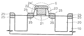
図19に示されるように、半導体基板10上にトレンチ素子分離膜20を形成する。次に、トレンチ素子分離膜20によって画定された活性領域上にゲート酸化膜21、ゲート電極22及び側壁スペーサ23よりなるゲート電極パターンGを形成する。そして、ゲート電極パターンG左右の活性領域及びゲート電極22の上部にのみ半導体物質膜24、例えばシリコン膜を選択的に成長させる。
As shown in FIG. 19, a trench
図20に示されるように、ゲート電極パターンGをイオン注入マスクとして導電型不純物、例えばn型不純物を注入してエレベイテッドソース/ドレイン領域25を形成する。この際、ゲート電極22の上部には不純物の注入された半導体物質膜24’が形成される。
As shown in FIG. 20, an elevated source /
図21に示されるように、サリサイド工程を行ってエレベイテッドソース/ドレイン領域25とゲート電極22の上部にシリサイド膜26を形成する。即ち、まずシリサイド膜26を形成するために遷移金属膜(図示せず)を半導体基板10の全面に形成する。次に、熱処理を行って遷移金属膜の一部をシリサイド膜26に変化させる。次に、シリサイド膜26に変化されない遷移金属膜を除去する。ところが、従来の技術によってエレベイテッドソース/ドレイン領域25の上部にシリサイド膜26を形成する場合には、図21のIIのように素子分離膜20とソース/ドレイン領域25の境界部でシリサイド膜26がソース/ドレイン領域25の内部にも拡張形成されてしまい、接合漏れ電流を発生させる。即ち、トレンチ素子分離膜20とエレベイテッドソース/ドレイン領域25の境界部に蒸着された遷移金属とが剰余のシリサイド膜ソース(シリサイド膜の供給源)として作用するために、前記境界部で前記シリサイド膜26が厚く形成されることになる。これにより、半導体素子の接合漏れ電流特性が劣化し、半導体素子の電力消耗量が増加する等の問題点を発生させることになる。
As shown in FIG. 21, a salicide process is performed to form a
本発明が解決しようとする技術的課題は、素子分離膜と活性領域との境界において発生する接合漏れ電流を軽減し得るソース/ドレイン領域の形成方法を提供することである。 A technical problem to be solved by the present invention is to provide a method for forming a source / drain region that can reduce a junction leakage current generated at a boundary between an element isolation film and an active region.
前記技術的課題を達成するための本発明に係るエレベイテッドサリサイドソース/ドレイン領域の形成方法は、まず、下部には第1幅及び第1深さを有する狭幅トレンチ領域を具備し、上部には前記第1幅より大きな第2幅及び前記第1深さより浅い第2深さを有する拡幅トレンチ領域を具備するT型素子分離膜を形成する。次に、前記T型素子分離膜により画定された活性領域上にゲート酸化膜、ゲート電極及び側壁スペーサよりなるゲート電極パターンを形成する。次に、前記ゲート電極パターンの左右に露出された前記活性領域上及び前記ゲート電極上に半導体物質膜を成長させ。その後、前記ゲート電極パターンをイオン注入マスクとして用いて、導電型不純物を前記半導体物質膜及び前記露出された活性領域に注入すると同時に、前記狭幅トレンチ領域の上端部から左右側に延長された前記拡幅トレンチ領域である前記T型素子分離膜のヘッド部の下部にも前記導電型不純物が注入されるように前記導電型不純物を注入して、エレベイテッドソース/ドレイン領域を形成する。次いで、前記エレベイテッドソース/ドレイン領域上にサリサイド工程によりシリサイド膜を形成する。 In order to achieve the above technical problem, the elevated salicide source / drain region forming method according to the present invention includes a narrow trench region having a first width and a first depth at a lower portion and an upper portion at a lower portion. Forms a T-type isolation layer having a widened trench region having a second width larger than the first width and a second depth shallower than the first depth. Next, a gate electrode pattern including a gate oxide film, a gate electrode, and a sidewall spacer is formed on the active region defined by the T-type element isolation film. Next, the semiconductor material layer is grown on the gate electrode on the active region exposed to the left and right pattern and the gate electrode. Thereafter, using the gate electrode pattern as an ion implantation mask , a conductive impurity is implanted into the semiconductor material film and the exposed active region, and at the same time, extended from the upper end of the narrow trench region to the left and right sides. wherein in the lower part of the head portion of the T-type isolation layer is widened trench region by injecting the conductive impurity as the conductivity type impurity is implanted to form the elevated source / drain regions. Next, a silicide film is formed on the elevated source / drain region by a salicide process .
前記拡幅トレンチ領域の深さは1000Å以下であることが望ましい。 The depth of the widened trench region is preferably 1000 mm or less.
前記半導体物質膜はSEG(Selective EpitaxialGrowth)、すなわち、選択エピタキシャル成長法を使用して形成することが望ましい。 The semiconductor material film is preferably formed using SEG (Selective Epitaxic Growth), that is, selective epitaxial growth.
前記シリサイド膜はチタン、タンタル、ニッケル、コバルトまたは白金のシリサイド膜のうちの少なくとも一つ以上を含むように構成できる。 The silicide film may include at least one of a silicide film of titanium, tantalum, nickel, cobalt, or platinum.
本発明に係るTエレベイテッドサリサイドソース/ドレイン領域の形成方法、および半導体素子は、素子分離膜とソース/ドレイン領域の境界部において発生する接合漏れ電流を軽減し得る。 The method for forming a T-elevated salicide source / drain region and a semiconductor element according to the present invention can reduce junction leakage current generated at the boundary between the element isolation film and the source / drain region.
以下、添付した図面に基づき、T型素子分離膜形成方法に対する第1及び第2実施例を詳しく説明した後、これを用いたエレベイテッドサリサイドソース/ドレイン領域の形成方法に対する実施例を詳しく説明する。しかし、本発明の実施例は多様な形態に変形でき、本発明の範囲は後述する実施例に限定されない。以下の図面に基づいた説明は当業者が十分に実施可能なように本発明を完全に説明するために提供されるものである。図面において層や領域等の厚さは説明の便宜上誇張されている。図面において同じ符号は同じ要素を指称する。また、何れかの層が別の層または基板の上部にあるという記載には、前記何れの層が別の層または基板の上部に直接存在する場合だけでなく、その間に第3の層が介在される場合も含む。 Hereinafter, the first and second embodiments of the T-type isolation layer forming method will be described in detail with reference to the accompanying drawings, and then the embodiment of the elevated salicide source / drain region forming method using the same will be described in detail. . However, the embodiments of the present invention can be modified in various forms, and the scope of the present invention is not limited to the embodiments described later. The following description based on the drawings is provided to fully describe the invention so that those skilled in the art can fully practice the invention. In the drawings, the thicknesses of layers and regions are exaggerated for convenience of explanation. In the drawings, the same reference numerals designate the same elements. In addition, the statement that any layer is on the top of another layer or substrate includes not only the case in which any of the layers is directly on the top of another layer or substrate, but also a third layer interposed therebetween. This includes cases where
図1に示されるように、本発明の第1実施例に係るT型素子分離膜形成方法は、まず、第1絶縁膜30と第2絶縁膜32を通常の方法、例えば化学気相蒸着法を使用して半導体基板10上に順次に形成する。第1絶縁膜30は熱酸化法で形成することができる。第2絶縁膜32は第1絶縁膜30に対してエッチング選択比の大きな物質膜で形成することが望ましい。例えば、第1絶縁膜30はシリコン酸化膜で形成し、第2絶縁膜32はシリコン窒化膜またはシリコン酸化窒化膜で形成することができる。第1絶縁膜30は100Å乃至500Åの厚さに形成し、第2絶縁膜32は500Å乃至2500Åの厚さに形成することができる。
As shown in FIG. 1, in the T-type device isolation film forming method according to the first embodiment of the present invention, first, the first insulating
図2に示されるように、フォトリソグラフィー工程を行って第1絶縁膜30及び第2絶縁膜32をパタニングすることによって、第1絶縁膜パターン30’と第2絶縁膜パターン32’とが積層された第1マスクパターン34を形成する。その後、第1マスクパターン34の側壁にスペーサ36を形成する。スペーサ36は第2絶縁膜パターン32’と同じ物質で形成することが望ましい。例えば、第2絶縁膜パターン32’をシリコン窒化膜で形成した場合、スペーサ36は次のように形成する。シリコン窒化膜を半導体基板10の全面に形成した後、異方性エッチング工程を実施して第1マスクパターン34の側壁にスペーサ36が形成されるまでシリコン窒化膜をエッチングする。一方、スペーサ36の下部が半導体基板10の上部表面と接触する幅W1は狭幅トレンチ領域の第1幅(後述する図4のW1参照)に応じて定められる。
As shown in FIG. 2, the first insulating
図3に示されるように、半導体基板10の全面に第1絶縁膜パターン30’と同じ物質を用いて絶縁膜を形成する。例えば、第1絶縁膜パターン30’がシリコン酸化膜の場合、前記絶縁膜もシリコン酸化膜で形成する。次いで、化学機械的研磨方法またはエッチバック方法を使用して絶縁膜を平坦化することによって、第2絶縁膜パターン32’の上部を露出させる。その結果、スペーサ36の間に第2マスクパターン40が形成される。一方、前記平坦化工程中に第2絶縁膜パターン32’も一部エッチングされるために、第2絶縁膜パターン32’の厚さは薄くなる。
As shown in FIG. 3, an insulating film is formed on the entire surface of the
図4に示されるように、第2絶縁膜パターン32’及びスペーサ36を除去して半導体基板10の上部表面を露出させる。次いで、第1絶縁膜パターン30’及び第2マスクパターン40をエッチングマスクとして使用するエッチング工程、例えば乾式エッチング工程を行って第1幅W1及び第1深さD1を有する狭幅トレンチ領域T1を形成する。狭幅トレンチ領域T1は隣接する半導体素子間の電気的分離を可能にしうる程度の深さに形成することが望ましい。従って、第1深さD1は2000Å乃至6000Åであることが望ましい。
As shown in FIG. 4, the second insulating
図5に示されるように、第1絶縁膜パターン30’及び第2マスクパターン40を通常の方法、例えば湿式エッチング方法を使用して除去する。それから、狭幅トレンチ領域T1を埋立てるために第1間隙充填絶縁膜46を形成する。第1間隙充填絶縁膜46はシリコン酸化膜またはシリコン酸化窒化膜で有ってもよい。第1間隙充填絶縁膜46を形成する前に、狭幅トレンチ領域T1の内部壁に沿って熱酸化膜(図示せず)を形成することもできる。また、熱酸化膜上に窒化膜ライナーを形成することもできる。第1間隙充填絶縁膜46は第1幅W1の1/2以上の厚さに形成することが望ましい。なぜなら、第1間隙充填絶縁膜46を第1幅W1の1/2以上の厚さに形成すれば、狭幅トレンチ領域T1を完全に埋立てられるからである。第1間隙充填絶縁膜46は化学気相蒸着法または熱酸化法で形成することができる。ただし、好適には、熱酸化方法で形成することが望ましい。なぜなら、化学気相蒸着法を用いることによって第1間隙充填絶縁膜46を形成すれば狭幅トレンチ領域内部にボイドが形成される可能性が大きくなり、一方、熱酸化方法を用いることにゆって第1間隙充填絶縁膜46を形成すれば狭幅トレンチ領域T1内にボイドが形成される可能性が小さくなるからである。
As shown in FIG. 5, the first insulating
一方、狭幅トレンチ領域T1の縦横比が3以上の場合には狭幅トレンチ領域T1内に充填された第1間隙充填絶縁膜46内にボイド(図示せず)が形成されることもあり得る。しかし、本発明に係るT型素子分離膜形成方法は、狭幅トレンチ領域T1内に充填された第1間隙充填絶縁膜46内にボイドが形成されてもボイドの開放を許容しない。これについては後述する。
On the other hand, when the aspect ratio of the narrow trench region T1 is 3 or more, a void (not shown) may be formed in the first gap filling insulating
図6に示されるように、第1間隙充填絶縁膜46を第2幅W2に露出させる第3マスクパターン48を第1間隙充填絶縁膜46上に形成する。第3マスクパターン48は第1間隙充填絶縁膜46に対するエッチング選択比の大きい物質で形成することが望ましい。例えば、第1間隙充填絶縁膜46がシリコン酸化膜の場合に第3マスクパターン48はシリコン窒化膜で形成することが望ましい。そして、第3マスクパターン48は500Å乃至2500Åの厚さに形成することができる。次いで、第3マスクパターン48をエッチングマスクとして使用するエッチング工程、例えば乾式エッチング工程を行って第1間隙充填絶縁膜46及び半導体基板10をエッチングして開口52を形成する。この際、開口52の縦横比が3以下になるように形成することが望ましい。その結果、第2幅W2及び第2深さD2を有する拡幅トレンチ領域T2が半導体基板10内に形成される。前記第2深さD2は500Å乃至4000Åで有り得る。勿論、第2深さD2は第1深さD1よりは小さく、第2幅W2は第1幅W1より大きい。一方、前述したように狭幅トレンチ領域T1内部に充填された第1間隙充填絶縁膜46内にはボイド(図示せず)が形成され得る。従って、拡幅トレンチ領域T2を形成する過程でボイドが開放され得る。しかし、後続する工程で拡幅トレンチ領域T2内部は第2間隙充填絶縁膜で充填されるため、開放されたボイド内部にも第2間隙充填絶縁膜が充填される。その結果、狭幅トレンチ領域T1内に形成されるボイドは開放されない。
As shown in FIG. 6, a
図7に示されるように、開口(図6の52参照)の内部及び第3マスクパターン48上に第2間隙充填絶縁膜54を形成する。第2間隙充填絶縁膜54はシリコン酸化膜であっても、シリコン酸化窒化膜であってもよい。次に、半導体基板10の全面を通常の方法、例えば化学機械的研磨方法またはエッチバック方法を使用して平坦化することによって、第3マスクパターン48を露出させる。第2間隙充填絶縁膜54を形成する前に、拡幅トレンチ領域T2の内壁にそって熱酸化膜(図示せず)を形成しうる。また、熱酸化膜上に窒化膜ライナー(図示せず)を形成することもできる。一方、第3マスクパターン48の上部及び開口(図6の52参照)の内部に第2間隙充填絶縁膜54を形成する前に、半導体基板10上に形成された第1間隙充填絶縁膜46及び第3マスクパターン48を除去することもできる。そうすると、拡幅トレンチ領域T2内部に充填された第2間隙充填絶縁膜54内のボイドの形成を確実に防止しうる。勿論、半導体基板10上に形成された第1間隙充填絶縁膜46及び第3マスクパターン48を除去することなく、半導体基板10上に第2間隙充填絶縁膜54を形成して拡幅トレンチ領域T2を埋めたてるとしてもボイドは形成されない。これは、開口(図6の52参照)の縦横比が3以下であるからである。
As shown in FIG. 7, a second gap filling insulating
図8に示されるように、半導体基板10の全面を平坦化して半導体基板10の上部を露出させると、T型素子分離膜56が形成される。
As shown in FIG. 8, when the entire surface of the
以上、本発明のT型素子分離膜形成方法に対する第1実施例を図面に基づいて詳しく説明した。第1実施例では狭幅トレンチ領域T1が拡幅トレンチ領域T2より先に形成され、狭幅トレンチ領域T1に絶縁物質を充填する工程と拡幅トレンチ領域T2に絶縁物質を充填する工程とは別に実施される場合を示した。 The first embodiment of the T-type element isolation film forming method of the present invention has been described in detail with reference to the drawings. In the first embodiment, the narrow trench region T1 is formed before the wide trench region T2, and the step of filling the narrow trench region T1 with an insulating material and the step of filling the wide trench region T2 with an insulating material are performed separately. Showed the case.
以下、本発明のT型素子分離膜形成方法に対する第2実施例を図面に基づいて詳しく説明する。第2実施例は第1実施例とは異なり、拡幅トレンチ領域T2が狭幅トレンチ領域T1より先に形成される。そして、狭幅トレンチ領域T1と拡幅トレンチ領域T2は単一の工程で絶縁物質に充填される。なお、狭幅トレンチ領域T1及び拡幅トレンチ領域T2の幅と深さに対して部材番号は第1実施例と同一な部材番号が使われる。 Hereinafter, a second embodiment of the T-type device isolation film forming method of the present invention will be described in detail with reference to the drawings. The second embodiment is different from the first embodiment in that the wide trench region T2 is formed before the narrow trench region T1. The narrow trench region T1 and the wide trench region T2 are filled with an insulating material in a single process. Note that the same member numbers as those in the first embodiment are used for the width and depth of the narrow trench region T1 and the wide trench region T2.
図9に示されるように、半導体基板10上にマスクパターン62を形成する。マスクパターン62はパッド酸化膜、シリコン窒化膜及びシリコン酸化膜を順次に積層した3重膜に形成しうる。または、シリコン酸化膜、シリコン窒化膜またはシリコン酸化窒化膜の単一膜またはこれらの組合よりなる二重膜に形成することもできる。マスクパターン62は1500Å乃至4000Åの厚さに形成することが可能である。次に、マスクパターン62をエッチングマスクとして使用して半導体基板10をエッチングする。その結果、第2幅W2及び第2深さD2を有する拡幅トレンチ領域T2が形成される。拡幅トレンチ領域T2は通常の方法、例えば乾式エッチング方法を使用して形成する。第2深さD2は500Å乃至4000Åとすることができる。
As shown in FIG. 9, a
図10に示されるように、マスクパターン62の上部及び拡幅トレンチ領域T2の内部に絶縁膜を形成する。次いで、絶縁膜を異方性エッチングしてマスクパターン62の側壁及び拡幅トレンチ領域T2の側壁にスペーサ66を形成する。スペーサ66はシリコン酸化膜、シリコン窒化膜またはシリコン酸化窒化膜で形成することが可能である。スペーサ66は拡幅トレンチ領域T2の全てが埋立てられない程度の厚さに形成する。
As shown in FIG. 10, an insulating film is formed on the
次に、マスクパターン62及びスペーサ66をエッチングマスクとして使用して拡幅トレンチ領域T2の下部に露出された半導体基板10をエッチングする。その結果、第1幅W1及び第1深さD1を有する狭幅トレンチ領域T1が形成される。狭幅トレンチ領域T1は隣接する半導体素子間の電気的分離が可能な深さに形成することが望ましい。従って、第1深さD1は2000Å乃至6000Åとすることができる。狭幅トレンチ領域T1は通常の方法、例えば乾式エッチング方法を使用して形成する。
Next, the
図11に示されるように、マスクパターン62及び側壁スペーサ66を除去する。次に、狭幅トレンチ領域T1及び拡幅トレンチ領域T2を充填する間隙充填絶縁膜68が形成される。間隙充填絶縁膜68はシリコン酸化膜、シリコン窒化膜またはシリコン酸化窒化膜とすることができる。間隙充填絶縁膜68は化学気相蒸着方法を使用して形成することが望ましい。これは、化学気相蒸着方法は段差塗布特性に優れるからである。一方、間隙充填絶縁膜68を形成する前に狭幅トレンチ領域T1及び拡幅トレンチ領域T2の内壁に沿って熱酸化膜(図示せず)を形成することもできる。また、熱酸化膜上に窒化膜ライナー(図示せず)を形成することもできる。
As shown in FIG. 11, the
一方、前記狭幅トレンチ領域T1の縦横比((D1−D2)/W1)が、3以上の場合、狭幅トレンチ領域T1の内にボイドが形成されうる。しかし、狭幅トレンチ領域T1内にトレンチが形成されても、広幅トレンチ領域T2内にはボイドが形成されないためボイドの開放を防ぐことができる。 On the other hand, when the aspect ratio ((D1-D2) / W1) of the narrow trench region T1 is 3 or more, a void may be formed in the narrow trench region T1. However, even if a trench is formed in the narrow trench region T1, no void is formed in the wide trench region T2, so that the opening of the void can be prevented.
一方、上記説明ではマスクパターン62及びスペーサ66を除去した後、間隙充填絶縁膜68を形成したが、本実施形態は、これに限られない。例えば、マスクパターン62及びスペーサ66を除去せず、間隙充填絶縁膜68を形成することもできる。マスクパターン62及びスペーサ66を除去せずに間隙充填絶縁膜68を形成すれば、工程数を減らすことができる。
On the other hand, in the above description, the gap filling insulating
図12に示されるように、間隙充填絶縁膜68の形成された半導体基板10の全面を化学機械的研磨方法またはエッチバック方法で平坦化することによって、半導体基板10の上部を露出させる。その結果、T型素子分離膜70が形成される。
As shown in FIG. 12, the upper surface of the
以下、前記第1及び第2実施例によって例示されたT型素子分離膜の形成方法を用いたエレベイテッドサリサイドソース/ドレイン領域の形成方法に対する実施例を説明する。 Hereinafter, an embodiment of a method for forming an elevated salicide source / drain region using the method for forming a T-type device isolation film exemplified in the first and second embodiments will be described.
図13に示されるように、狭幅トレンチ領域T1及び拡幅トレンチ領域T2内に間隙充填絶縁膜の充填されたT型素子分離膜71を形成する。T型素子分離膜71を形成する方法に対しては前述した通りである。但し、拡幅トレンチ領域T2の深さD2を適切に調節することによって、ソース/ドレイン領域を形成するイオン注入工程でT型素子分離膜71のヘッド部を構成して狭幅トレンチ領域の上端部から左右側に延長された拡幅トレンチ領域T2の下部(図15の81参照)にも不純物を注入可能にする。従って、拡幅トレンチ領域T2の深さD2は1000Å以下になるように形成することが望ましい。次に、T型素子分離膜71によって画定される活性領域上にゲート酸化膜72が介在されゲート電極74及びスペーサ76からなるゲート電極パターンGを形成する。スペーサ76をゲート酸化膜72及びゲート電極74の側壁に形成する前に、ゲート電極74をイオン注入マスクとして使用して低濃度の導電型不純物、例えばn型不純物を注入することもできる。
As shown in FIG. 13, a T-type
図14に示されるように、ゲート電極パターンG左右の露出された半導体基板10の表面及びゲート電極74の上部表面に半導体物質膜78を成長させる。半導体物質膜78はシリコン膜、ゲルマニウム膜またはシリコンとゲルマニウムの化合物膜とすることができる。半導体物質膜78はSEG(Selective Epitaxial Growth)法(選択エピタキシャル成長法)によって形成することが望ましい。
As shown in FIG. 14, a
図15に示されるように、ゲート電極パターンGをイオン注入マスクとして導電型不純物、例えばn型不純物を注入する。その結果、エレベイテッドソース/ドレイン領域80が形成される。また、ゲート電極74の上部には不純物のドーピングされた半導体物質膜78’が形成される。エレベイテッドソース/ドレイン領域80の形成のためのイオン注入において、注入される導電型不純物イオンのエネルギーは形成しようとするpn接合の深さに応じてその大きさを調節する。特に、T型素子分離膜71のヘッド部を構成し、狭幅トレンチ領域の上端部から左右側に延長された拡幅トレンチ領域の下部81にも不純物が注入されるように、注入される導電型不純物イオンのエネルギーを調節する。不純物を注入してエレベイテッドソース/ドレイン領域80を形成した後、熱処理工程を行って注入された導電型不純物を活性化する。側壁スペーサ76の形成前にゲート電極74の左右に低濃度の導電型不純物を注入した場合には、ゲート電極パターンGをイオン注入マスクとして使用するイオン注入工程によりLDD(Lightly Dopped Drain:図示せず)構造が形成される。
As shown in FIG. 15, a conductive impurity, for example, an n-type impurity is implanted using the gate electrode pattern G as an ion implantation mask. As a result, an elevated source /
図16に示されるように、ゲート電極74の上部及びエレベイテッドソース/ドレイン領域80の上部にシリサイド膜82を形成するためにサリサイド工程を進行する。まず、半導体基板10全面に遷移金属膜を形成する。次いで、ゲート電極74の上部及びエレベイテッドソース/ドレイン領域80の上部表面に自己整列(セルフアライメント)されたシリサイド膜82が形成されるように熱処理を行う。前記遷移金属膜はチタン膜、タンタル膜、コバルト膜、クロム膜、ニッケル膜、白金膜またはこれらの組合膜とすることができる。一方、0.2μm級のデザインルールを有する半導体素子を製造する場合にはシリサイド化のための熱処理方法を選択するに当って注意を要する。なぜなら、通常の熱処理方法でシリサイド膜を形成すれば、エレベイテッドソース/ドレイン領域80に注入された導電型不純物が熱拡散され、トランジスタの素子特性(降伏電圧等)が劣化されるからである。従って、急速熱処理工程を使用し、遷移金属膜をシリサイド化することが望ましい。
As shown in FIG. 16, a salicide process is performed to form a
ゲート電極74の上部及びエレベイテッドソース/ドレイン領域80の上部にシリサイド膜82を形成した後、シリサイド膜82に変化されていない遷移金属膜を除去する。図16のIIIから分かるように、T型素子分離膜71のヘッド部を構成し、狭幅トレンチ領域の上端部から左右側に延長された拡幅トレンチ領域の下部81にも不純物を注入すれば、T型素子分離膜71とエレベイテッドソース/ドレイン領域80の境界部でシリサイド膜が厚く形成されても、接合の深さを十分に確保できる。その結果、素子分離膜とソース/ドレイン領域の境界部から発生する接合漏れ電流を緩和しうる。
After the
本発明に係るT型素子分離膜を含む半導体素子に対する実施例は、本発明に係るT型素子分離膜の形成方法に対する実施例を説明しながら開示したことがあるので略す。 An example of a semiconductor element including a T-type element isolation film according to the present invention is omitted because it has been disclosed while describing an example of a method for forming a T-type element isolation film according to the present invention.
以上、望ましい実施例によって本発明を具体的に説明したが、本発明はこれに限定されず、本発明の技術的思想の範囲内で当業者によってその変形や改良が可能である。 Although the present invention has been specifically described with reference to the preferred embodiments, the present invention is not limited to this, and modifications and improvements can be made by those skilled in the art within the scope of the technical idea of the present invention.
10 半導体基板、
56 T型素子分離膜。
10 Semiconductor substrate,
56 T-type element isolation membrane.
Claims (4)
(b)前記T型素子分離膜により画定された活性領域上にゲート酸化膜、ゲート電極及びスペーサよりなるゲート電極パターンを形成する段階と、
(c)前記ゲート電極パターンの左右に露出された前記活性領域上及び前記ゲート電極上に半導体物質膜を成長させる段階と、
(d)前記ゲート電極パターンをイオン注入マスクとして用いて、導電型不純物を前記半導体物質膜及び前記露出された活性領域に注入すると同時に、前記狭幅トレンチ領域の上端部から左右側に延長された前記拡幅トレンチ領域である前記T型素子分離膜のヘッド部の下部にも前記導電型不純物が注入されるように前記導電型不純物を注入して、エレベイテッドソース/ドレイン領域を形成する段階と、
(e)前記エレベイテッドソース/ドレイン領域上にサリサイド工程によりシリサイド膜を形成する段階と、
を含むエレベイテッドサリサイドソース/ドレイン領域の形成方法。 (A) A narrow trench region having a first width and a first depth is provided in a lower portion, and a wide trench having a second width wider than the first width and a second depth shallower than the first depth in an upper portion. Forming a T-type element isolation film having a region;
(B) forming a gate electrode pattern comprising a gate oxide film, a gate electrode and a spacer on the active region defined by the T-type element isolation film;
(C) growing a semiconductor material film on the active region and on the gate electrode exposed to the left and right of the gate electrode pattern;
(D) Using the gate electrode pattern as an ion implantation mask , a conductive impurity is implanted into the semiconductor material film and the exposed active region, and at the same time extended from the upper end of the narrow trench region to the left and right sides. Implanting the conductive impurities to form the elevated source / drain regions so that the conductive impurities are also implanted below the head portion of the T-type element isolation film, which is the widening trench region;
(E) forming a silicide film on the elevated source / drain region by a salicide process ;
A method of forming an elevated salicide source / drain region including:
Applications Claiming Priority (2)
| Application Number | Priority Date | Filing Date | Title |
|---|---|---|---|
| KR19990018268 | 1999-05-20 | ||
| KR1019990043784A KR100338766B1 (en) | 1999-05-20 | 1999-10-11 | Method of Elevated Salicide Source/Drain Region Using method of Forming T-Shape Isolation Layer and Semiconductor Device using thereof |
Related Parent Applications (1)
| Application Number | Title | Priority Date | Filing Date |
|---|---|---|---|
| JP2000150672A Division JP3998893B2 (en) | 1999-05-20 | 2000-05-22 | Method for forming T-type element isolation film |
Publications (2)
| Publication Number | Publication Date |
|---|---|
| JP2006066927A JP2006066927A (en) | 2006-03-09 |
| JP4446949B2 true JP4446949B2 (en) | 2010-04-07 |
Family
ID=26635197
Family Applications (2)
| Application Number | Title | Priority Date | Filing Date |
|---|---|---|---|
| JP2000150672A Expired - Fee Related JP3998893B2 (en) | 1999-05-20 | 2000-05-22 | Method for forming T-type element isolation film |
| JP2005280957A Expired - Fee Related JP4446949B2 (en) | 1999-05-20 | 2005-09-27 | Method for forming elevated salicide source / drain regions |
Family Applications Before (1)
| Application Number | Title | Priority Date | Filing Date |
|---|---|---|---|
| JP2000150672A Expired - Fee Related JP3998893B2 (en) | 1999-05-20 | 2000-05-22 | Method for forming T-type element isolation film |
Country Status (4)
| Country | Link |
|---|---|
| US (2) | US6383877B1 (en) |
| JP (2) | JP3998893B2 (en) |
| KR (1) | KR100338766B1 (en) |
| TW (1) | TW516162B (en) |
Families Citing this family (46)
| Publication number | Priority date | Publication date | Assignee | Title |
|---|---|---|---|---|
| KR100630664B1 (en) * | 2000-05-09 | 2006-10-02 | 삼성전자주식회사 | Integrated circuit elements with cooling system |
| JP3650022B2 (en) * | 2000-11-13 | 2005-05-18 | 三洋電機株式会社 | Manufacturing method of semiconductor device |
| US6921947B2 (en) * | 2000-12-15 | 2005-07-26 | Renesas Technology Corp. | Semiconductor device having recessed isolation insulation film |
| US6727558B1 (en) * | 2001-02-15 | 2004-04-27 | Advanced Micro Devices, Inc. | Channel isolation using dielectric isolation structures |
| JP2003060024A (en) * | 2001-08-13 | 2003-02-28 | Mitsubishi Electric Corp | Semiconductor device manufacturing method and semiconductor device |
| KR100402392B1 (en) * | 2001-11-06 | 2003-10-17 | 삼성전자주식회사 | Semiconductor device having trench isolation structure and method of fabricating the same |
| KR100414735B1 (en) * | 2001-12-10 | 2004-01-13 | 주식회사 하이닉스반도체 | A semiconductor device and A method for forming the same |
| KR20030050785A (en) * | 2001-12-19 | 2003-06-25 | 주식회사 하이닉스반도체 | Method of manufacturing a semiconductor device |
| KR20030050784A (en) * | 2001-12-19 | 2003-06-25 | 주식회사 하이닉스반도체 | Method of manufacturing a semiconductor device |
| KR100400782B1 (en) * | 2001-12-27 | 2003-10-08 | 주식회사 하이닉스반도체 | Method for fabricating of semiconductor device |
| KR100412144B1 (en) * | 2002-05-16 | 2003-12-31 | 주식회사 하이닉스반도체 | Method for manufacturing semiconductor device |
| KR100466207B1 (en) * | 2002-07-04 | 2005-01-13 | 매그나칩 반도체 유한회사 | Method for manufacturing a semiconductor device |
| US6833602B1 (en) * | 2002-09-06 | 2004-12-21 | Lattice Semiconductor Corporation | Device having electrically isolated low voltage and high voltage regions and process for fabricating the device |
| US20040256671A1 (en) * | 2003-06-17 | 2004-12-23 | Kuo-Tai Huang | Metal-oxide-semiconductor transistor with selective epitaxial growth film |
| US7402207B1 (en) | 2004-05-05 | 2008-07-22 | Advanced Micro Devices, Inc. | Method and apparatus for controlling the thickness of a selective epitaxial growth layer |
| KR100669664B1 (en) * | 2004-09-14 | 2007-01-15 | 동부일렉트로닉스 주식회사 | Semiconductor device and manufacturing method |
| US7456062B1 (en) | 2004-10-20 | 2008-11-25 | Advanced Micro Devices, Inc. | Method of forming a semiconductor device |
| US7402485B1 (en) | 2004-10-20 | 2008-07-22 | Advanced Micro Devices, Inc. | Method of forming a semiconductor device |
| US7402886B2 (en) * | 2004-11-23 | 2008-07-22 | Sandisk Corporation | Memory with self-aligned trenches for narrow gap isolation regions |
| US7276433B2 (en) * | 2004-12-03 | 2007-10-02 | Micron Technology, Inc. | Methods of forming integrated circuitry, methods of forming memory circuitry, and methods of forming field effect transistors |
| KR100593452B1 (en) * | 2005-02-01 | 2006-06-28 | 삼성전자주식회사 | Manufacturing method of MOS transistor having all silicide metal gate electrode |
| US7553732B1 (en) | 2005-06-13 | 2009-06-30 | Advanced Micro Devices, Inc. | Integration scheme for constrained SEG growth on poly during raised S/D processing |
| US20060281271A1 (en) * | 2005-06-13 | 2006-12-14 | Advanced Micro Devices, Inc. | Method of forming a semiconductor device having an epitaxial layer and device thereof |
| US20070235783A9 (en) * | 2005-07-19 | 2007-10-11 | Micron Technology, Inc. | Semiconductor constructions, memory arrays, electronic systems, and methods of forming semiconductor constructions |
| US7772672B2 (en) | 2005-09-01 | 2010-08-10 | Micron Technology, Inc. | Semiconductor constructions |
| US7572705B1 (en) | 2005-09-21 | 2009-08-11 | Advanced Micro Devices, Inc. | Semiconductor device and method of manufacturing a semiconductor device |
| KR100707593B1 (en) * | 2005-12-27 | 2007-04-13 | 동부일렉트로닉스 주식회사 | Double device isolation structure of semiconductor device and its formation method |
| JP2007220739A (en) * | 2006-02-14 | 2007-08-30 | Sony Corp | Semiconductor device, method for manufacturing the same, and method for forming silicon oxynitride film |
| US20070194403A1 (en) * | 2006-02-23 | 2007-08-23 | International Business Machines Corporation | Methods for fabricating semiconductor device structures with reduced susceptibility to latch-up and semiconductor device structures formed by the methods |
| US7799694B2 (en) | 2006-04-11 | 2010-09-21 | Micron Technology, Inc. | Methods of forming semiconductor constructions |
| KR100810409B1 (en) * | 2006-10-31 | 2008-03-04 | 주식회사 하이닉스반도체 | Device Separator Formation Method of Semiconductor Device |
| CN101847607B (en) * | 2009-03-27 | 2014-08-20 | 联华电子股份有限公司 | Technology of flash memory and insulation structure applied to flash memory |
| KR101201903B1 (en) * | 2010-07-20 | 2012-11-16 | 매그나칩 반도체 유한회사 | Element isolation structure of semiconductor and method for forming the same |
| US9054221B2 (en) * | 2011-08-31 | 2015-06-09 | Institute of Microelectronics, Chinese Academy of Sciences | Semiconductor device with a common back gate isolation region and method for manufacturing the same |
| US9214400B2 (en) * | 2011-08-31 | 2015-12-15 | Institute of Microelectronics, Chinese Academy of Sciences | Semiconductor device with back gate isolation regions and method for manufacturing the same |
| US8623713B2 (en) * | 2011-09-15 | 2014-01-07 | International Business Machines Corporation | Trench isolation structure |
| US20130093062A1 (en) * | 2011-10-18 | 2013-04-18 | Ying-Chih Lin | Semiconductor structure and process thereof |
| US20140327084A1 (en) | 2013-05-01 | 2014-11-06 | International Business Machines Corporation | Dual shallow trench isolation (sti) field effect transistor (fet) and methods of forming |
| KR102072410B1 (en) | 2013-08-07 | 2020-02-03 | 삼성전자 주식회사 | Semiconductor device and fabricated method thereof |
| US9379106B2 (en) | 2013-08-22 | 2016-06-28 | Samsung Electronics Co., Ltd. | Semiconductor devices having 3D channels, and methods of fabricating semiconductor devices having 3D channels |
| KR102025309B1 (en) * | 2013-08-22 | 2019-09-25 | 삼성전자 주식회사 | Semiconductor device and fabricated method thereof |
| CN106960789B (en) * | 2016-01-08 | 2020-03-10 | 中芯国际集成电路制造(上海)有限公司 | Semiconductor device and method for improving performance of semiconductor device |
| US20170278925A1 (en) * | 2016-03-23 | 2017-09-28 | Globalfoundries Inc. | Introducing material with a lower etch rate to form a t-shaped sdb sti structure |
| CN110299398B (en) | 2018-03-22 | 2022-04-19 | 联华电子股份有限公司 | High voltage transistor and method of manufacturing the same |
| JP2020129654A (en) * | 2019-01-18 | 2020-08-27 | ヘリオス バイオエレクトロニクス インコーポレイテッド | Method of multi-level etching, semiconductor sensing device, and method for manufacturing semiconductor sensing device |
| CN118156125A (en) * | 2023-12-19 | 2024-06-07 | 杭州富芯半导体有限公司 | Semiconductor device and method for manufacturing the same |
Family Cites Families (12)
| Publication number | Priority date | Publication date | Assignee | Title |
|---|---|---|---|---|
| US4472240A (en) * | 1981-08-21 | 1984-09-18 | Tokyo Shibaura Denki Kabushiki Kaisha | Method for manufacturing semiconductor device |
| JP2635796B2 (en) * | 1990-04-03 | 1997-07-30 | 株式会社東芝 | Rolling control device |
| JPH05343509A (en) * | 1992-06-05 | 1993-12-24 | Hitachi Ltd | Method for manufacturing semiconductor integrated circuit device |
| US5242847A (en) | 1992-07-27 | 1993-09-07 | North Carolina State University At Raleigh | Selective deposition of doped silion-germanium alloy on semiconductor substrate |
| US5536675A (en) * | 1993-12-30 | 1996-07-16 | Intel Corporation | Isolation structure formation for semiconductor circuit fabrication |
| KR100329061B1 (en) * | 1994-03-15 | 2002-11-13 | 내셔널 세미콘덕터 코포레이션 | Planarized trench and field oxide isolation scheme |
| JP3329640B2 (en) * | 1995-10-10 | 2002-09-30 | 株式会社東芝 | Method for manufacturing semiconductor device |
| US5874317A (en) * | 1996-06-12 | 1999-02-23 | Advanced Micro Devices, Inc. | Trench isolation for integrated circuits |
| US5824586A (en) * | 1996-10-23 | 1998-10-20 | Advanced Micro Devices, Inc. | Method of manufacturing a raised source/drain MOSFET |
| TW358989B (en) * | 1997-04-08 | 1999-05-21 | United Microelectronics Corp | Method of forming gold-oxygen semiconductor cells |
| US6121100A (en) * | 1997-12-31 | 2000-09-19 | Intel Corporation | Method of fabricating a MOS transistor with a raised source/drain extension |
| US6165871A (en) * | 1999-07-16 | 2000-12-26 | Chartered Semiconductor Manufacturing Ltd. | Method of making low-leakage architecture for sub-0.18 μm salicided CMOS device |
-
1999
- 1999-10-11 KR KR1019990043784A patent/KR100338766B1/en not_active Expired - Lifetime
-
2000
- 2000-05-18 US US09/573,268 patent/US6383877B1/en not_active Expired - Lifetime
- 2000-05-22 JP JP2000150672A patent/JP3998893B2/en not_active Expired - Fee Related
- 2000-05-26 TW TW089110345A patent/TW516162B/en not_active IP Right Cessation
-
2002
- 2002-01-15 US US10/044,991 patent/US6624496B2/en not_active Expired - Lifetime
-
2005
- 2005-09-27 JP JP2005280957A patent/JP4446949B2/en not_active Expired - Fee Related
Also Published As
| Publication number | Publication date |
|---|---|
| JP3998893B2 (en) | 2007-10-31 |
| KR20000075409A (en) | 2000-12-15 |
| US6383877B1 (en) | 2002-05-07 |
| JP2006066927A (en) | 2006-03-09 |
| TW516162B (en) | 2003-01-01 |
| US6624496B2 (en) | 2003-09-23 |
| US20020090795A1 (en) | 2002-07-11 |
| KR100338766B1 (en) | 2002-05-30 |
| JP2000357733A (en) | 2000-12-26 |
Similar Documents
| Publication | Publication Date | Title |
|---|---|---|
| JP4446949B2 (en) | Method for forming elevated salicide source / drain regions | |
| KR100282452B1 (en) | Semiconductor device and method for fabricating the same | |
| KR100574338B1 (en) | Metal gate formation method of semiconductor device | |
| US7071048B2 (en) | Methods of fabricating fin field effect transistors having capping insulation layers | |
| US6737308B2 (en) | Semiconductor device having LDD-type source/drain regions and fabrication method thereof | |
| US8168492B2 (en) | Field effect transistors with vertically oriented gate electrodes and methods for fabricating the same | |
| US6649481B2 (en) | Methods of fabricating a semiconductor device structure for manufacturing high-density and high-performance integrated-circuits | |
| US6204137B1 (en) | Method to form transistors and local interconnects using a silicon nitride dummy gate technique | |
| US20070184623A1 (en) | Semiconductor device comprising buried channel region and method for manufacturing the same | |
| US6165871A (en) | Method of making low-leakage architecture for sub-0.18 μm salicided CMOS device | |
| JP2005072577A (en) | Highly integrated semiconductor device having silicide film capable of ensuring contact margin and method for manufacturing the same | |
| JP4394385B2 (en) | Semiconductor device and manufacturing method thereof | |
| KR101608902B1 (en) | Semiconductor device having a device isolation structure | |
| US7122431B2 (en) | Methods of fabrication metal oxide semiconductor (MOS) transistors having buffer regions below source and drain regions | |
| US7851853B2 (en) | Semiconductor device comprising high-withstand voltage MOSFET and its manufacturing method | |
| US6130121A (en) | Method for fabricating a transistor | |
| KR20040069515A (en) | MOSFET having recessed channel and fabricating method thereof | |
| KR100480236B1 (en) | Method for manufacturing semiconductor device | |
| KR100280517B1 (en) | Manufacturing method of semiconductor device | |
| KR20070020919A (en) | Recess channel array transistor and method of manufacturing same | |
| KR100734259B1 (en) | Manufacturing Method of Semiconductor Device | |
| JP2005223196A (en) | Semiconductor device and manufacturing method thereof | |
| KR100606952B1 (en) | Transistor Formation Method of Semiconductor Device | |
| JP2001203348A (en) | Semiconductor device and manufacturing method thereof | |
| KR20060046909A (en) | Method for manufacturing transistor with recess channel |
Legal Events
| Date | Code | Title | Description |
|---|---|---|---|
| A977 | Report on retrieval |
Free format text: JAPANESE INTERMEDIATE CODE: A971007 Effective date: 20090827 |
|
| A131 | Notification of reasons for refusal |
Free format text: JAPANESE INTERMEDIATE CODE: A131 Effective date: 20090908 |
|
| A521 | Request for written amendment filed |
Free format text: JAPANESE INTERMEDIATE CODE: A523 Effective date: 20091208 |
|
| TRDD | Decision of grant or rejection written | ||
| A01 | Written decision to grant a patent or to grant a registration (utility model) |
Free format text: JAPANESE INTERMEDIATE CODE: A01 Effective date: 20100105 |
|
| A01 | Written decision to grant a patent or to grant a registration (utility model) |
Free format text: JAPANESE INTERMEDIATE CODE: A01 |
|
| A61 | First payment of annual fees (during grant procedure) |
Free format text: JAPANESE INTERMEDIATE CODE: A61 Effective date: 20100119 |
|
| FPAY | Renewal fee payment (event date is renewal date of database) |
Free format text: PAYMENT UNTIL: 20130129 Year of fee payment: 3 |
|
| R150 | Certificate of patent or registration of utility model |
Free format text: JAPANESE INTERMEDIATE CODE: R150 |
|
| FPAY | Renewal fee payment (event date is renewal date of database) |
Free format text: PAYMENT UNTIL: 20130129 Year of fee payment: 3 |
|
| S111 | Request for change of ownership or part of ownership |
Free format text: JAPANESE INTERMEDIATE CODE: R313113 |
|
| FPAY | Renewal fee payment (event date is renewal date of database) |
Free format text: PAYMENT UNTIL: 20130129 Year of fee payment: 3 |
|
| R360 | Written notification for declining of transfer of rights |
Free format text: JAPANESE INTERMEDIATE CODE: R360 |
|
| FPAY | Renewal fee payment (event date is renewal date of database) |
Free format text: PAYMENT UNTIL: 20130129 Year of fee payment: 3 |
|
| R350 | Written notification of registration of transfer |
Free format text: JAPANESE INTERMEDIATE CODE: R350 |
|
| R250 | Receipt of annual fees |
Free format text: JAPANESE INTERMEDIATE CODE: R250 |
|
| S531 | Written request for registration of change of domicile |
Free format text: JAPANESE INTERMEDIATE CODE: R313531 |
|
| S533 | Written request for registration of change of name |
Free format text: JAPANESE INTERMEDIATE CODE: R313533 |
|
| R350 | Written notification of registration of transfer |
Free format text: JAPANESE INTERMEDIATE CODE: R350 |
|
| R250 | Receipt of annual fees |
Free format text: JAPANESE INTERMEDIATE CODE: R250 |
|
| LAPS | Cancellation because of no payment of annual fees |