US6825129B2 - Method for manufacturing memory device - Google Patents
Method for manufacturing memory device Download PDFInfo
- Publication number
- US6825129B2 US6825129B2 US10/153,614 US15361402A US6825129B2 US 6825129 B2 US6825129 B2 US 6825129B2 US 15361402 A US15361402 A US 15361402A US 6825129 B2 US6825129 B2 US 6825129B2
- Authority
- US
- United States
- Prior art keywords
- layer
- forming
- bst
- cvd
- interlayer insulating
- Prior art date
- Legal status (The legal status is an assumption and is not a legal conclusion. Google has not performed a legal analysis and makes no representation as to the accuracy of the status listed.)
- Expired - Fee Related
Links
- 238000000034 method Methods 0.000 title claims abstract description 89
- 238000004519 manufacturing process Methods 0.000 title claims abstract description 15
- 238000005229 chemical vapour deposition Methods 0.000 claims abstract description 28
- 239000004065 semiconductor Substances 0.000 claims abstract description 13
- 239000010410 layer Substances 0.000 claims description 226
- 230000008569 process Effects 0.000 claims description 31
- 238000003860 storage Methods 0.000 claims description 26
- 239000011229 interlayer Substances 0.000 claims description 25
- 238000000151 deposition Methods 0.000 claims description 22
- 230000004888 barrier function Effects 0.000 claims description 21
- 229910021420 polycrystalline silicon Inorganic materials 0.000 claims description 19
- 229920005591 polysilicon Polymers 0.000 claims description 19
- 229910052751 metal Inorganic materials 0.000 claims description 18
- 239000002184 metal Substances 0.000 claims description 18
- 239000000758 substrate Substances 0.000 claims description 16
- 238000005530 etching Methods 0.000 claims description 15
- 238000006243 chemical reaction Methods 0.000 claims description 11
- 239000000463 material Substances 0.000 claims description 11
- 238000007669 thermal treatment Methods 0.000 claims description 11
- 229910052741 iridium Inorganic materials 0.000 claims description 7
- 229910052697 platinum Inorganic materials 0.000 claims description 7
- 229910052707 ruthenium Inorganic materials 0.000 claims description 7
- 238000001039 wet etching Methods 0.000 claims description 7
- 238000011049 filling Methods 0.000 claims description 6
- 229910052737 gold Inorganic materials 0.000 claims description 6
- 229910052750 molybdenum Inorganic materials 0.000 claims description 6
- 229910052759 nickel Inorganic materials 0.000 claims description 6
- 229920002120 photoresistant polymer Polymers 0.000 claims description 6
- 229910052709 silver Inorganic materials 0.000 claims description 6
- 150000004767 nitrides Chemical class 0.000 claims description 5
- 238000004380 ashing Methods 0.000 claims description 4
- 238000005240 physical vapour deposition Methods 0.000 claims description 4
- 229910021332 silicide Inorganic materials 0.000 claims description 4
- FVBUAEGBCNSCDD-UHFFFAOYSA-N silicide(4-) Chemical compound [Si-4] FVBUAEGBCNSCDD-UHFFFAOYSA-N 0.000 claims description 4
- 229910052814 silicon oxide Inorganic materials 0.000 claims description 4
- 229910008482 TiSiN Inorganic materials 0.000 claims description 3
- 229910008486 TiSix Inorganic materials 0.000 claims description 3
- ATJFFYVFTNAWJD-UHFFFAOYSA-N Tin Chemical compound [Sn] ATJFFYVFTNAWJD-UHFFFAOYSA-N 0.000 claims description 3
- QRXWMOHMRWLFEY-UHFFFAOYSA-N isoniazide Chemical compound NNC(=O)C1=CC=NC=C1 QRXWMOHMRWLFEY-UHFFFAOYSA-N 0.000 claims description 3
- 238000005498 polishing Methods 0.000 claims description 3
- 239000000126 substance Substances 0.000 claims description 3
- 229910052718 tin Inorganic materials 0.000 claims description 3
- 206010010144 Completed suicide Diseases 0.000 claims 1
- 239000003990 capacitor Substances 0.000 abstract description 20
- 229910052454 barium strontium titanate Inorganic materials 0.000 description 42
- 238000000231 atomic layer deposition Methods 0.000 description 17
- 239000002243 precursor Substances 0.000 description 16
- BASFCYQUMIYNBI-UHFFFAOYSA-N platinum Chemical compound [Pt] BASFCYQUMIYNBI-UHFFFAOYSA-N 0.000 description 8
- 239000000203 mixture Substances 0.000 description 7
- 238000010926 purge Methods 0.000 description 7
- 239000007789 gas Substances 0.000 description 6
- 230000008021 deposition Effects 0.000 description 5
- 229910010252 TiO3 Inorganic materials 0.000 description 4
- 239000003989 dielectric material Substances 0.000 description 4
- 230000010354 integration Effects 0.000 description 4
- OKKJLVBELUTLKV-UHFFFAOYSA-N Methanol Chemical group OC OKKJLVBELUTLKV-UHFFFAOYSA-N 0.000 description 3
- 230000008901 benefit Effects 0.000 description 3
- 238000002425 crystallisation Methods 0.000 description 3
- 230000008025 crystallization Effects 0.000 description 3
- 238000006557 surface reaction Methods 0.000 description 3
- XZPXMWMVWDSEMY-UHFFFAOYSA-N 2,2,3-trimethyloctane Chemical compound CCCCCC(C)C(C)(C)C XZPXMWMVWDSEMY-UHFFFAOYSA-N 0.000 description 2
- 229910015802 BaSr Inorganic materials 0.000 description 2
- IMNFDUFMRHMDMM-UHFFFAOYSA-N N-Heptane Chemical compound CCCCCCC IMNFDUFMRHMDMM-UHFFFAOYSA-N 0.000 description 2
- GWEVSGVZZGPLCZ-UHFFFAOYSA-N Titan oxide Chemical compound O=[Ti]=O GWEVSGVZZGPLCZ-UHFFFAOYSA-N 0.000 description 2
- MCMNRKCIXSYSNV-UHFFFAOYSA-N Zirconium dioxide Chemical compound O=[Zr]=O MCMNRKCIXSYSNV-UHFFFAOYSA-N 0.000 description 2
- 238000007796 conventional method Methods 0.000 description 2
- 238000005137 deposition process Methods 0.000 description 2
- 125000001301 ethoxy group Chemical group [H]C([H])([H])C([H])([H])O* 0.000 description 2
- 239000007788 liquid Substances 0.000 description 2
- 125000000956 methoxy group Chemical group [H]C([H])([H])O* 0.000 description 2
- 238000012986 modification Methods 0.000 description 2
- 230000004048 modification Effects 0.000 description 2
- 230000001105 regulatory effect Effects 0.000 description 2
- WOCIAKWEIIZHES-UHFFFAOYSA-N ruthenium(iv) oxide Chemical compound O=[Ru]=O WOCIAKWEIIZHES-UHFFFAOYSA-N 0.000 description 2
- 229910052712 strontium Inorganic materials 0.000 description 2
- 241000790917 Dioxys <bee> Species 0.000 description 1
- UFHFLCQGNIYNRP-UHFFFAOYSA-N Hydrogen Chemical compound [H][H] UFHFLCQGNIYNRP-UHFFFAOYSA-N 0.000 description 1
- -1 Methoxy Pentane Chemical compound 0.000 description 1
- 229910020684 PbZr Inorganic materials 0.000 description 1
- 229910052777 Praseodymium Inorganic materials 0.000 description 1
- 229910004491 TaAlN Inorganic materials 0.000 description 1
- 229910004166 TaN Inorganic materials 0.000 description 1
- 229910003071 TaON Inorganic materials 0.000 description 1
- 229910004200 TaSiN Inorganic materials 0.000 description 1
- RTAQQCXQSZGOHL-UHFFFAOYSA-N Titanium Chemical compound [Ti] RTAQQCXQSZGOHL-UHFFFAOYSA-N 0.000 description 1
- 238000007792 addition Methods 0.000 description 1
- 150000004703 alkoxides Chemical class 0.000 description 1
- 238000000137 annealing Methods 0.000 description 1
- QVGXLLKOCUKJST-UHFFFAOYSA-N atomic oxygen Chemical compound [O] QVGXLLKOCUKJST-UHFFFAOYSA-N 0.000 description 1
- 229910052788 barium Inorganic materials 0.000 description 1
- DSAJWYNOEDNPEQ-UHFFFAOYSA-N barium atom Chemical compound [Ba] DSAJWYNOEDNPEQ-UHFFFAOYSA-N 0.000 description 1
- 230000033228 biological regulation Effects 0.000 description 1
- 230000015572 biosynthetic process Effects 0.000 description 1
- 238000009835 boiling Methods 0.000 description 1
- 239000012159 carrier gas Substances 0.000 description 1
- 239000003153 chemical reaction reagent Substances 0.000 description 1
- 238000004140 cleaning Methods 0.000 description 1
- 239000002131 composite material Substances 0.000 description 1
- 239000013078 crystal Substances 0.000 description 1
- 230000003247 decreasing effect Effects 0.000 description 1
- 230000006866 deterioration Effects 0.000 description 1
- 238000009792 diffusion process Methods 0.000 description 1
- 230000000694 effects Effects 0.000 description 1
- 238000005516 engineering process Methods 0.000 description 1
- 238000011066 ex-situ storage Methods 0.000 description 1
- 230000006870 function Effects 0.000 description 1
- 238000010574 gas phase reaction Methods 0.000 description 1
- 239000001257 hydrogen Substances 0.000 description 1
- 229910052739 hydrogen Inorganic materials 0.000 description 1
- 238000011065 in-situ storage Methods 0.000 description 1
- HTXDPTMKBJXEOW-UHFFFAOYSA-N iridium(IV) oxide Inorganic materials O=[Ir]=O HTXDPTMKBJXEOW-UHFFFAOYSA-N 0.000 description 1
- 230000000873 masking effect Effects 0.000 description 1
- 238000002156 mixing Methods 0.000 description 1
- OFBQJSOFQDEBGM-UHFFFAOYSA-N n-pentane Natural products CCCCC OFBQJSOFQDEBGM-UHFFFAOYSA-N 0.000 description 1
- 230000003647 oxidation Effects 0.000 description 1
- 238000007254 oxidation reaction Methods 0.000 description 1
- 239000001301 oxygen Substances 0.000 description 1
- 229910052760 oxygen Inorganic materials 0.000 description 1
- 238000009832 plasma treatment Methods 0.000 description 1
- 238000000926 separation method Methods 0.000 description 1
- 239000007787 solid Substances 0.000 description 1
- 238000001179 sorption measurement Methods 0.000 description 1
- CIOAGBVUUVVLOB-UHFFFAOYSA-N strontium atom Chemical compound [Sr] CIOAGBVUUVVLOB-UHFFFAOYSA-N 0.000 description 1
- 238000006467 substitution reaction Methods 0.000 description 1
- PBCFLUZVCVVTBY-UHFFFAOYSA-N tantalum pentoxide Inorganic materials O=[Ta](=O)O[Ta](=O)=O PBCFLUZVCVVTBY-UHFFFAOYSA-N 0.000 description 1
Images


Classifications
-
- H—ELECTRICITY
- H10—SEMICONDUCTOR DEVICES; ELECTRIC SOLID-STATE DEVICES NOT OTHERWISE PROVIDED FOR
- H10B—ELECTRONIC MEMORY DEVICES
- H10B99/00—Subject matter not provided for in other groups of this subclass
-
- H—ELECTRICITY
- H01—ELECTRIC ELEMENTS
- H01L—SEMICONDUCTOR DEVICES NOT COVERED BY CLASS H10
- H01L21/00—Processes or apparatus adapted for the manufacture or treatment of semiconductor or solid state devices or of parts thereof
- H01L21/02—Manufacture or treatment of semiconductor devices or of parts thereof
- H01L21/02104—Forming layers
- H01L21/02107—Forming insulating materials on a substrate
- H01L21/02225—Forming insulating materials on a substrate characterised by the process for the formation of the insulating layer
- H01L21/0226—Forming insulating materials on a substrate characterised by the process for the formation of the insulating layer formation by a deposition process
- H01L21/02263—Forming insulating materials on a substrate characterised by the process for the formation of the insulating layer formation by a deposition process deposition from the gas or vapour phase
- H01L21/02271—Forming insulating materials on a substrate characterised by the process for the formation of the insulating layer formation by a deposition process deposition from the gas or vapour phase deposition by decomposition or reaction of gaseous or vapour phase compounds, i.e. chemical vapour deposition
-
- C—CHEMISTRY; METALLURGY
- C23—COATING METALLIC MATERIAL; COATING MATERIAL WITH METALLIC MATERIAL; CHEMICAL SURFACE TREATMENT; DIFFUSION TREATMENT OF METALLIC MATERIAL; COATING BY VACUUM EVAPORATION, BY SPUTTERING, BY ION IMPLANTATION OR BY CHEMICAL VAPOUR DEPOSITION, IN GENERAL; INHIBITING CORROSION OF METALLIC MATERIAL OR INCRUSTATION IN GENERAL
- C23C—COATING METALLIC MATERIAL; COATING MATERIAL WITH METALLIC MATERIAL; SURFACE TREATMENT OF METALLIC MATERIAL BY DIFFUSION INTO THE SURFACE, BY CHEMICAL CONVERSION OR SUBSTITUTION; COATING BY VACUUM EVAPORATION, BY SPUTTERING, BY ION IMPLANTATION OR BY CHEMICAL VAPOUR DEPOSITION, IN GENERAL
- C23C16/00—Chemical coating by decomposition of gaseous compounds, without leaving reaction products of surface material in the coating, i.e. chemical vapour deposition [CVD] processes
- C23C16/02—Pretreatment of the material to be coated
- C23C16/0272—Deposition of sub-layers, e.g. to promote the adhesion of the main coating
-
- C—CHEMISTRY; METALLURGY
- C23—COATING METALLIC MATERIAL; COATING MATERIAL WITH METALLIC MATERIAL; CHEMICAL SURFACE TREATMENT; DIFFUSION TREATMENT OF METALLIC MATERIAL; COATING BY VACUUM EVAPORATION, BY SPUTTERING, BY ION IMPLANTATION OR BY CHEMICAL VAPOUR DEPOSITION, IN GENERAL; INHIBITING CORROSION OF METALLIC MATERIAL OR INCRUSTATION IN GENERAL
- C23C—COATING METALLIC MATERIAL; COATING MATERIAL WITH METALLIC MATERIAL; SURFACE TREATMENT OF METALLIC MATERIAL BY DIFFUSION INTO THE SURFACE, BY CHEMICAL CONVERSION OR SUBSTITUTION; COATING BY VACUUM EVAPORATION, BY SPUTTERING, BY ION IMPLANTATION OR BY CHEMICAL VAPOUR DEPOSITION, IN GENERAL
- C23C16/00—Chemical coating by decomposition of gaseous compounds, without leaving reaction products of surface material in the coating, i.e. chemical vapour deposition [CVD] processes
- C23C16/22—Chemical coating by decomposition of gaseous compounds, without leaving reaction products of surface material in the coating, i.e. chemical vapour deposition [CVD] processes characterised by the deposition of inorganic material, other than metallic material
- C23C16/30—Deposition of compounds, mixtures or solid solutions, e.g. borides, carbides, nitrides
- C23C16/40—Oxides
- C23C16/409—Oxides of the type ABO3 with A representing alkali, alkaline earth metal or lead and B representing a refractory metal, nickel, scandium or a lanthanide
-
- C—CHEMISTRY; METALLURGY
- C23—COATING METALLIC MATERIAL; COATING MATERIAL WITH METALLIC MATERIAL; CHEMICAL SURFACE TREATMENT; DIFFUSION TREATMENT OF METALLIC MATERIAL; COATING BY VACUUM EVAPORATION, BY SPUTTERING, BY ION IMPLANTATION OR BY CHEMICAL VAPOUR DEPOSITION, IN GENERAL; INHIBITING CORROSION OF METALLIC MATERIAL OR INCRUSTATION IN GENERAL
- C23C—COATING METALLIC MATERIAL; COATING MATERIAL WITH METALLIC MATERIAL; SURFACE TREATMENT OF METALLIC MATERIAL BY DIFFUSION INTO THE SURFACE, BY CHEMICAL CONVERSION OR SUBSTITUTION; COATING BY VACUUM EVAPORATION, BY SPUTTERING, BY ION IMPLANTATION OR BY CHEMICAL VAPOUR DEPOSITION, IN GENERAL
- C23C16/00—Chemical coating by decomposition of gaseous compounds, without leaving reaction products of surface material in the coating, i.e. chemical vapour deposition [CVD] processes
- C23C16/44—Chemical coating by decomposition of gaseous compounds, without leaving reaction products of surface material in the coating, i.e. chemical vapour deposition [CVD] processes characterised by the method of coating
- C23C16/455—Chemical coating by decomposition of gaseous compounds, without leaving reaction products of surface material in the coating, i.e. chemical vapour deposition [CVD] processes characterised by the method of coating characterised by the method used for introducing gases into reaction chamber or for modifying gas flows in reaction chamber
- C23C16/45523—Pulsed gas flow or change of composition over time
- C23C16/45525—Atomic layer deposition [ALD]
- C23C16/45527—Atomic layer deposition [ALD] characterized by the ALD cycle, e.g. different flows or temperatures during half-reactions, unusual pulsing sequence, use of precursor mixtures or auxiliary reactants or activations
- C23C16/45531—Atomic layer deposition [ALD] characterized by the ALD cycle, e.g. different flows or temperatures during half-reactions, unusual pulsing sequence, use of precursor mixtures or auxiliary reactants or activations specially adapted for making ternary or higher compositions
-
- C—CHEMISTRY; METALLURGY
- C23—COATING METALLIC MATERIAL; COATING MATERIAL WITH METALLIC MATERIAL; CHEMICAL SURFACE TREATMENT; DIFFUSION TREATMENT OF METALLIC MATERIAL; COATING BY VACUUM EVAPORATION, BY SPUTTERING, BY ION IMPLANTATION OR BY CHEMICAL VAPOUR DEPOSITION, IN GENERAL; INHIBITING CORROSION OF METALLIC MATERIAL OR INCRUSTATION IN GENERAL
- C23C—COATING METALLIC MATERIAL; COATING MATERIAL WITH METALLIC MATERIAL; SURFACE TREATMENT OF METALLIC MATERIAL BY DIFFUSION INTO THE SURFACE, BY CHEMICAL CONVERSION OR SUBSTITUTION; COATING BY VACUUM EVAPORATION, BY SPUTTERING, BY ION IMPLANTATION OR BY CHEMICAL VAPOUR DEPOSITION, IN GENERAL
- C23C16/00—Chemical coating by decomposition of gaseous compounds, without leaving reaction products of surface material in the coating, i.e. chemical vapour deposition [CVD] processes
- C23C16/56—After-treatment
-
- H—ELECTRICITY
- H01—ELECTRIC ELEMENTS
- H01L—SEMICONDUCTOR DEVICES NOT COVERED BY CLASS H10
- H01L21/00—Processes or apparatus adapted for the manufacture or treatment of semiconductor or solid state devices or of parts thereof
- H01L21/02—Manufacture or treatment of semiconductor devices or of parts thereof
- H01L21/02104—Forming layers
- H01L21/02107—Forming insulating materials on a substrate
- H01L21/02109—Forming insulating materials on a substrate characterised by the type of layer, e.g. type of material, porous/non-porous, pre-cursors, mixtures or laminates
- H01L21/02112—Forming insulating materials on a substrate characterised by the type of layer, e.g. type of material, porous/non-porous, pre-cursors, mixtures or laminates characterised by the material of the layer
- H01L21/02172—Forming insulating materials on a substrate characterised by the type of layer, e.g. type of material, porous/non-porous, pre-cursors, mixtures or laminates characterised by the material of the layer the material containing at least one metal element, e.g. metal oxides, metal nitrides, metal oxynitrides or metal carbides
- H01L21/02197—Forming insulating materials on a substrate characterised by the type of layer, e.g. type of material, porous/non-porous, pre-cursors, mixtures or laminates characterised by the material of the layer the material containing at least one metal element, e.g. metal oxides, metal nitrides, metal oxynitrides or metal carbides the material having a perovskite structure, e.g. BaTiO3
-
- H—ELECTRICITY
- H01—ELECTRIC ELEMENTS
- H01L—SEMICONDUCTOR DEVICES NOT COVERED BY CLASS H10
- H01L21/00—Processes or apparatus adapted for the manufacture or treatment of semiconductor or solid state devices or of parts thereof
- H01L21/02—Manufacture or treatment of semiconductor devices or of parts thereof
- H01L21/04—Manufacture or treatment of semiconductor devices or of parts thereof the devices having potential barriers, e.g. a PN junction, depletion layer or carrier concentration layer
- H01L21/18—Manufacture or treatment of semiconductor devices or of parts thereof the devices having potential barriers, e.g. a PN junction, depletion layer or carrier concentration layer the devices having semiconductor bodies comprising elements of Group IV of the Periodic Table or AIIIBV compounds with or without impurities, e.g. doping materials
- H01L21/30—Treatment of semiconductor bodies using processes or apparatus not provided for in groups H01L21/20 - H01L21/26
- H01L21/31—Treatment of semiconductor bodies using processes or apparatus not provided for in groups H01L21/20 - H01L21/26 to form insulating layers thereon, e.g. for masking or by using photolithographic techniques; After treatment of these layers; Selection of materials for these layers
- H01L21/314—Inorganic layers
- H01L21/316—Inorganic layers composed of oxides or glassy oxides or oxide based glass
- H01L21/31691—Inorganic layers composed of oxides or glassy oxides or oxide based glass with perovskite structure
-
- H—ELECTRICITY
- H10—SEMICONDUCTOR DEVICES; ELECTRIC SOLID-STATE DEVICES NOT OTHERWISE PROVIDED FOR
- H10D—INORGANIC ELECTRIC SEMICONDUCTOR DEVICES
- H10D1/00—Resistors, capacitors or inductors
- H10D1/60—Capacitors
- H10D1/68—Capacitors having no potential barriers
- H10D1/682—Capacitors having no potential barriers having dielectrics comprising perovskite structures
- H10D1/684—Capacitors having no potential barriers having dielectrics comprising perovskite structures the dielectrics comprising multiple layers, e.g. comprising buffer layers, seed layers or gradient layers
-
- H—ELECTRICITY
- H01—ELECTRIC ELEMENTS
- H01L—SEMICONDUCTOR DEVICES NOT COVERED BY CLASS H10
- H01L21/00—Processes or apparatus adapted for the manufacture or treatment of semiconductor or solid state devices or of parts thereof
- H01L21/02—Manufacture or treatment of semiconductor devices or of parts thereof
- H01L21/02104—Forming layers
- H01L21/02107—Forming insulating materials on a substrate
- H01L21/02225—Forming insulating materials on a substrate characterised by the process for the formation of the insulating layer
- H01L21/0226—Forming insulating materials on a substrate characterised by the process for the formation of the insulating layer formation by a deposition process
- H01L21/02263—Forming insulating materials on a substrate characterised by the process for the formation of the insulating layer formation by a deposition process deposition from the gas or vapour phase
- H01L21/02271—Forming insulating materials on a substrate characterised by the process for the formation of the insulating layer formation by a deposition process deposition from the gas or vapour phase deposition by decomposition or reaction of gaseous or vapour phase compounds, i.e. chemical vapour deposition
- H01L21/0228—Forming insulating materials on a substrate characterised by the process for the formation of the insulating layer formation by a deposition process deposition from the gas or vapour phase deposition by decomposition or reaction of gaseous or vapour phase compounds, i.e. chemical vapour deposition deposition by cyclic CVD, e.g. ALD, ALE, pulsed CVD
-
- H—ELECTRICITY
- H01—ELECTRIC ELEMENTS
- H01L—SEMICONDUCTOR DEVICES NOT COVERED BY CLASS H10
- H01L21/00—Processes or apparatus adapted for the manufacture or treatment of semiconductor or solid state devices or of parts thereof
- H01L21/02—Manufacture or treatment of semiconductor devices or of parts thereof
- H01L21/04—Manufacture or treatment of semiconductor devices or of parts thereof the devices having potential barriers, e.g. a PN junction, depletion layer or carrier concentration layer
- H01L21/18—Manufacture or treatment of semiconductor devices or of parts thereof the devices having potential barriers, e.g. a PN junction, depletion layer or carrier concentration layer the devices having semiconductor bodies comprising elements of Group IV of the Periodic Table or AIIIBV compounds with or without impurities, e.g. doping materials
- H01L21/30—Treatment of semiconductor bodies using processes or apparatus not provided for in groups H01L21/20 - H01L21/26
- H01L21/31—Treatment of semiconductor bodies using processes or apparatus not provided for in groups H01L21/20 - H01L21/26 to form insulating layers thereon, e.g. for masking or by using photolithographic techniques; After treatment of these layers; Selection of materials for these layers
- H01L21/314—Inorganic layers
- H01L21/316—Inorganic layers composed of oxides or glassy oxides or oxide based glass
- H01L21/3165—Inorganic layers composed of oxides or glassy oxides or oxide based glass formed by oxidation
- H01L21/31683—Inorganic layers composed of oxides or glassy oxides or oxide based glass formed by oxidation of metallic layers, e.g. Al deposited on the body, e.g. formation of multi-layer insulating structures
Definitions
- the present invention relates to a semiconductor memory device and to a method for manufacturing capacitors in a semiconductor memory device.
- a memory cell region for storing 1 bit which is a unit of storage in the memory device, becomes decreased. Meanwhile, an area of a capacitor may not decrease as much as that of the unit cells. This is because a capacitance charge per cell is needed to prevent soft error and to maintain an operational safety margin. Therefore, there are three methods for maintaining proper memory capacitance within a limited cell region.
- the first method reduces the thickness of a dielectric.
- the second method makes a capacitor bottom electrify with a three-dimensional structure with a large effective area.
- the third method uses high dielectric constant materials.
- a dielectric layer capacitor has a high dielectric constant material such as TiO 2 , Ta 2 O 5 , ZrO 2 , (BaSr)TiO 3 (BST), (PbZr)TiO 3 (PZT), (PbLa) (ZrTi)O 3 (PLZT), (PbLa)TiO 3 (PLT), TaON, etc.
- the barium strontium titanate (BST) layer is expected to be a preferred high dielectric layer, which is adapted to 0.10 ⁇ m technology.
- the BST dielectric layer has a high dielectric constant of about 200 to 400, and it is crystallized on a metal layer, so it has a metal-insulator-metal (MIM) structure.
- the metal layer which is used as an electrode, can be any material selected from Pr, Ir, Ru, RuO 2 or IrO 2 .
- the BST layer itself is unstable, and therefore makes an etching process of a metal electrode so difficult as to cause many problems in the integration process, like deterioration caused by hydrogen.
- a barrier layer is necessarily formed. The barrier layer prevents reaction with a polysilicon plug, and prevents diffusion of oxygen, which is used as a source in depositing a dielectric layer and annealing the dielectric layer.
- the conventional art utilizes a concave capacitor to avoid the difficulties associated with the etching process.
- an interlayer insulating layer is formed on a portion where a bottom electrode is formed, and a storage node hole is formed within the interlayer insulating layer.
- a platinum metal layer which is a bottom electrode, is deposited at a predetermined thickness to form a storage electrode.
- a platinum metal etching process is easily performed, and the height of a storage node may be regulated to prevent misalignment between a storage node contact and the storage node.
- FIG. 1 is a cross-sectional view of a conventional concave capacitor.
- a first interlayer insulating layer 205 is deposited on a semiconductor substrate 200 to form a contact hole, and a plug 210 is formed by filling the contact hole with a conducting layer.
- a second interlayer insulating layer 215 is deposited to form a concave capacitor and a storage node hole is formed.
- a bottom electrode 220 , a CVD-BST layer 225 and a top electrode 230 are consecutively formed on the storage node hole thereon.
- electric characteristics are unstable and produce a high leakage current, etc., due to the composition difference between Ba+Sr and Ti in CVD-BST process. This problem is generated when a gas phase reaction in the CVD deposition process causes unstable surface reactions according to the topology. Since the BST capacitor has sensitive electric characteristics, the above-mentioned problem as a large effect on the reliability of the whole device.
- an object of the present invention to provide a method for manufacturing a memory device having a BST capacitor in a concave structure by using the atomic layer deposition (ALD) capable of providing a good step-coverage of a dielectric material therein and by using the chemical vapor deposition (CVD) method in forming other thick layers required to form the BST capacitor.
- ALD atomic layer deposition
- CVD chemical vapor deposition
- the invention in part, pertains to a method for manufacturing a memory device having a dielectric layer, which includes forming a seed layer as a first dielectric layer by using a ALD method, and forming a second dielectric layer by using a CVD method.
- the first dielectric layer can be an ALD-BST layer
- the second dielectric layer can be a CVD-BST layer.
- the invention in part, pertains to a method for manufacturing a memory device which includes the steps of: forming a first interlayer insulating layer having a contact hole on a semiconductor substrate, forming a contact plug that is connected to the semiconductor substrate, forming a second interlayer insulating layer on the first interlayer insulating layer and the contact plug, forming a storage node hole by applying a selective etching process to the second interlayer insulating layer, thereby exposing the contact plug, forming a bottom electrode pattern on the exposed contact plug, successively forming an ALD-BST layer and a CVD-BST layer on the bottom electrode to form a dielectric layer, and depositing a top electrode on the dielectric layer.
- the first interlayer insulating layer includes oxide and nitride layers, and the nitride layer forms at a thickness of about 300 ⁇ to about 1000 ⁇ .
- the invention in part, pertains to the step of forming the contact plug, in which includes the steps of forming a contact hole by applying a selective etching process to the first interlayer insulating layer, filling the contact hole with a polysilicon layer and applying an etch back process to the polysilicon layer to form a recess, and filling the recess with a silicide or barrier metal layer.
- the polysilicon layer can be a doped polysilicon layer formed at a thickness of about 500 ⁇ to about 3000 ⁇ using chemical vapor deposition.
- the plug recess has a depth of about 500 ⁇ to about 1500 ⁇ .
- the silicide layer is a TiSi x layer which is formed by forming a Ti layer on the plug recess at a thickness of about 100 ⁇ to about 300 ⁇ , applying a thermal treatment to the Ti layer, and removing a non-reaction Ti layer using a wet etching process.
- the barrier metal layer can be any one of TiN, TiSiN, TaAIN and a mixed layer thereof, and the barrier metal layer is deposited by a PVD or CVD method. Also, filling the recess is performed by applying a planarization process to the barrier metal layer by a chemical mechanical polishing method.
- the invention in part, pertains to the second interlayer insulating layer being formed by successively depositing an etching barrier layer, an oxide layer and a reflection barrier layer.
- the etching barrier layer can be a SiON layer.
- the invention in part, pertains to the step of forming the bottom electrode pattern including forming a conductive layer on the resulting structure including the storage node hole, forming a sacrificial layer on the conductive layer within the storage node hole, removing a portion of the conductive layer and a portion of the sacrificial layer in order to separate the conductive layer into a plurality of bottom electrodes, and removing the remnant of the sacrificial layer.
- the conductive layer may be any one of Ru, Pt, Ir, Os, W, Mo, Co, Ni, Au or Ag.
- the conductive layer is deposited by a CVD method and the conductive layer is formed at a thickness of about 50 ⁇ to about 500 ⁇ and at a substrate temperature of about 200° C. to about 500° C.
- the invention in part, pertains to the sacrificial layer being formed with a photoresist layer or an oxide layer.
- the sacrificial layer is a photoresist layer
- a portion of the sacrificial layer is removed by an ashing process after being separated into the bottom electrodes.
- the sacrificial layer is an oxide layer
- a portion of sacrificial layer is removed by a wet etching process after being separated into the bottom electrodes.
- the ALD-BST layer is formed at a temperature of about 150° C. to about 300° C. and at a thickness of about 20 ⁇ to about 100 ⁇ .
- a plasma thermal treatment is performed in an atmosphere comprising at least one of N 2 O, H 2 or O 2 for about 30 to about 180 seconds and at a temperature of about 300° C. to about 400° C., and power is applied in a range of about 100 W to about 1 kW.
- the CVD-BST layer can be deposited at a substrate temperature of about 400° C. to about 600° C. and at a thickness of 50 ⁇ to 200 ⁇ .
- a rapid thermal nitridation (RTN) is performed in an atmosphere of N 2 or N 2 O 2 gas, and a thermal treatment is carried out for about 30 to about 180 seconds and at a temperature of about 500° C. to about 700° C.
- the top electrode is any of Ru, Pt, Ir, Os, W, Mo, Co, Ni, Au and Ag, and the top electrode is formed by a CVD method.
- FIG. 1 is a cross-sectional view illustrating a conventional method for manufacturing a semiconductor device.
- FIGS. 2 to 6 are cross-sectional views illustrating a method for manufacturing a semiconductor device in accordance with an embodiment of the present invention.
- a (BaSr)TiO 3 (BST) layer which is used as a dielectric material in the invention, is a crystal having a perovskite structure.
- the BST layer is deposited by using an atomic layer deposition (ALD) method (hereinafter, referred to as an ALD-BST) and then it is also deposited by using a chemical vapor deposition (CVD) method (hereinafter, referred to as a CVD-BST).
- ALD atomic layer deposition
- CVD chemical vapor deposition
- the ALD method is similar to a CVD method from the viewpoint of chemical reactions between precursors. However, they are different from each other in that the conventional CVD method uses reactions between the precursors in a vapor state, while the ALD method uses surface reactions between two precursors.
- the ALD reaction precursor itself dissociates at the reaction temperature, and a reaction between the adsorbed and the supplied precursors takes place on the surface of the substrate.
- a source vapor is supplied with a carrier gas, which can be at least one of N 2 , Ar, etc.
- ALD process which uses a surface reaction
- the precursor is absorbed at all sites where chemisorptions are possible. If an excess quantity is provided, then the excess does not contribute to the reaction. The residual vapor is removed by a purge gas. Then, another kind of precursor is supplied and adsorbed to the surface to make a reaction, so the layers are always grown in an equal speed.
- one purge cycle “A” supply->N 2 (or Ar) purge->“B” supply->N 2 (or Ar) purge, is repeated to grow layers, and the growth speed denotes a layer thickness deposited for the one cycle.
- the layer is deposited by the above-mentioned deposition process, so that all the exposed surface has a similar possibility of adsorption of the precursor molecules regardless of its roughness. If the supplied precursors are sufficient, the layer is deposited in the same speed, regardless of an aspect ratio of surface structure. Also, since the above-mentioned method uses a one-by-one stacking method, it is possible to regulate precise control in thickness and composition of the layer.
- the ALD method when comparing with CVD, has another advantage in that a more complicated three dimensional layer deposition is possible.
- a layer composition is determined according to a thermal reaction of reagent gases, so a composition regulation thereof is not easy.
- the ALD method makes it possible to form a more complicated layer by alternating a plurality of atomic layers on a basis of the unit thickness of an atom.
- an ALD layer is deposited by using a mixture, i.e., a cocktail source of (Ba+Sr) and a Ti source.
- a cocktail source of (Ba+Sr) it is manufactured by mixing a mole fraction of 0.5:0.5 Ba:Sr in a solution, and the liquid concentration may be regulated to adapt a Ba:Sr:Ti composition of 0.25:0.25:0.5.
- a first cycle for depositing an ALD-BST layer uses H 2 O vapor is used as an O 2 source.
- the sequence for the first cycle is as follows: (Ba+Sr) cocktail source flow->N 2 (or Ar) purge->H 2 O vapor flow->N 2 or Ar) purge->Ti flow->N 2 (or Ar) purge->H 2 O vapor flow->N 2 (or Ar) purge.
- the first BST formation restricts a gas phase of CVD, then step coverage can be obtained in a storage node equally at a low temperature by using the ALD method. Then, the first BST layer is crystallized by plasma treatment using a low thermal budget. Finally a second BST layer is formed by using the CVD process for a post-layer process in a stacked layer. As a result, the boundary between the BST and a bottom electrode, which greatly affects the leakage current, may be effectively adjusted. Also, a BST seed layer deposited by the ALD method may decrease the thermal budget for a barrier metal to thereby manufacture a BST capacitor having good electric characteristics and reliability.
- FIG. 2 is a cross-sectional view illustrating a method for manufacturing a semiconductor device in accordance with a preferred embodiment of the invention.
- a first interlayer insulating layer 115 which includes an oxide layer 105 and a nitride layer (SiON) 110 as an anti-reflection layer, is formed on a semiconductor substrate 100 at a thickness of about 300 ⁇ to 1000 ⁇ , and a storage contact hole is connected to an active region (not shown) of the semiconductor substrate 100 through the first interlayer insulating layer 115 .
- a doped polysilicon layer is deposited on the storage contact hole at a thickness of about 500 ⁇ to 3000 ⁇ by using the CVD method.
- a surface of the first interlayer insulating layer 115 is exposed by etching back the doped polysilicon layer.
- the doped polysilicon layer undergoes an over etching process to form a polysilicon layer 120 only inside of a plug. Therefore, the contact hole is not completely filled with the polysilicon 120 , and the polysilicon 120 is recessed to have an extra space on a top region thereof.
- the plug recess has a height of about 500 ⁇ to 1500 ⁇ .
- a cleaning process is performed, and a Ti layer is deposited at a thickness of about 100 ⁇ to 300 ⁇ on the resulting structure.
- a thermal treatment is carried out by using a rapid thermal processing (RTP) method to form a TiSi x layer 125 , then a non-active Ti layer is removed by a wet etching process.
- RTP rapid thermal processing
- WN and W layers may be used to substitute for the Ti layer.
- This silicide layer 125 is formed to reduce contact resistance by forming ohmic contact with a polysilicon layer before forming a barrier metal.
- barrier metal is deposited on the resulting structure of the substrate, and planarized by using a chemical mechanical polishing (CMP) method.
- CMP chemical mechanical polishing
- a barrier metal is diffused and causes polysilicon oxidation in a surface of the polysilicon layer 120 for the plug and in an interface between the polysilicon layer 120 and a storage electrode.
- a barrier metal 130 can be any of TiN, TaN, TiSiN, TaSiN or TaAlN, and composite materials thereof, and a physical vapor deposition (PVD) or CVD can be used as a deposition method.
- a second interlayer insulating layer 150 is formed to form a storage node of a concave capacitor.
- the second interlayer insulating layer 150 is composed of an etch stopper 135 , an oxide layer 140 and an anti-reflection layer 145 .
- a SiON layer is deposited as the etch stopper 135 , and the oxide layer 140 and the anti-reflection layer 145 are deposited over the etch stopper, and then a storage node 155 are consecutively formed by carrying out a photo masking and an etching process.
- FIG. 3 is a cross-sectional view after depositing a conductive layer 160 for a bottom electrode.
- the conductive layer 160 is deposited using a CVD method.
- the conductive layer 160 can be any appropriate material such as at least one Ru, Pt, Ir, Os, W, Mo, Co, Ni, Au or Ag.
- the conductive layer 160 is formed at a thickness of about 50 ⁇ to 500 ⁇ and at a temperature of about 200° C. to 500° C.
- FIG. 4 is a cross-sectional view after forming a bottom electrode pattern 160 a and an ALD-BST layer 165 with the storage node separation.
- a sacrificial layer which has enough thickness to fully fill the inside of the storage hole on a resulting material where the bottom electrode conductive layer, is deposited.
- the sacrificial layer may be formed with a photoresist layer or an oxide layer.
- a portion of the bottom electrode and the sacrificial layer are removed until a top portion of the interlayer insulating layer is exposed by using the etch back or the CMP method to separate the bottom electrode into a plurality of electrodes. At this time, a residual remnant of the sacrificial layer may still exist inside of the storage node hole, and on the bottom electrode.
- the residual remnant of the sacrificial layer is removed by using an ashing or a wet etching process.
- a portion of the sacrificial layer is removed by using the ashing process.
- the sacrificial layer is made of an oxide layer, the portion of the sacrificial layer is removed by using a wet etching process.
- a thin BST layer 165 is deposited at a low temperature by using an ALD depositing method, and then a plasma thermal treatment is performed.
- a first cycle for depositing the ALD-BST layer follows the following sequence.
- the (Ba+Sr) cocktail source is methanol into which Ba(metmhd)2[Methoxy Ethoxy Tetramethyl Heptane Dionato Barium] and Sr(metmhd)2[Methoxy Ethoxy Tetramethyl Heptane Dionato Strontium] are dissolved.
- the Ti source includes a Ti alkoxide Ti(mpd) (tmhd)2[Methoxy Pentane Dioxy Tetamethyl Heptane Dionato Titanate].
- a deposition temperature is about 150° C. to 300° C. The deposition is carried out for about 20 to 100 cycles to adjust the thickness from about 20 ⁇ to 100 ⁇ .
- Each source, H 2 O and purge gas is modulated at flow rates of about 20 sccm to 80 sccm.
- a delivery time of (Ba+Sr) of the cocktail source is about 0.1 second to 1.0 second, the purge gas about 1.0 to 5.0 seconds and the H 2 O vapor about 0.1 to 1.0 seconds.
- the Ti flow rate is controlled between about 0.1 second to 1.0 second according to the Ti target composition.
- the plasma thermal treatment is performed in a N 2 O, N 2 or O 2 atmosphere to increase ALD-CVD crystallization in-situ or ex-situ.
- a temperature of the substrate is about 300° C. to 400° C., and power is applied for about 30 to 180 seconds in a range of about 100 W to 1 kW.
- FIG. 5 is a cross-sectional view after forming a CVD-BST layer 170 .
- the deposition of the CVD-BST 170 layer is carried out at a temperature of about 400° C. to 600° C., and to a thickness of about 50 ⁇ to 200 ⁇ .
- a thermal treatment to crystallize a dielectric material is carried out.
- the thermal treatment is performed by a rapid thermal nitridation (RTN) method. This RTN is performed in a N 2 or N 2 O 2 atmosphere for about 30 to 180 seconds and at a temperature of about 500° C. to 700° C.
- RTN rapid thermal nitridation
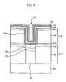
- FIG. 6 is a cross-sectional view after depositing a top electrode 175 .
- the top electrode 175 is formed a material that can be at least one of Ru, Pt, Ir, Os, W, Mo, Co, Ni, Au or Ag, and it is deposited by a CVD method.
- the invention is applicable to a BST capacitor in a high integration DRAM or FRAM having high aspect ratio.
- the ALD-BST layer is used as a seed layer of CVD-BST in a deep hole of a storage node. Accordingly, the invention has good step coverage and improves crystallization and uniformity of the dielectric layer. Also, since the invention uses a low temperature deposition, the BST capacitor has low leakage current and high reliability.
Landscapes
- Chemical & Material Sciences (AREA)
- Engineering & Computer Science (AREA)
- Materials Engineering (AREA)
- Chemical Kinetics & Catalysis (AREA)
- Microelectronics & Electronic Packaging (AREA)
- General Physics & Mathematics (AREA)
- Manufacturing & Machinery (AREA)
- Computer Hardware Design (AREA)
- Condensed Matter Physics & Semiconductors (AREA)
- Power Engineering (AREA)
- Physics & Mathematics (AREA)
- General Chemical & Material Sciences (AREA)
- Mechanical Engineering (AREA)
- Metallurgy (AREA)
- Organic Chemistry (AREA)
- Inorganic Chemistry (AREA)
- Semiconductor Memories (AREA)
Abstract
Description
Claims (22)
Applications Claiming Priority (2)
| Application Number | Priority Date | Filing Date | Title |
|---|---|---|---|
| KR2001-32745 | 2001-06-12 | ||
| KR10-2001-0032745A KR100418581B1 (en) | 2001-06-12 | 2001-06-12 | Method of forming memory device |
Publications (2)
| Publication Number | Publication Date |
|---|---|
| US20020187578A1 US20020187578A1 (en) | 2002-12-12 |
| US6825129B2 true US6825129B2 (en) | 2004-11-30 |
Family
ID=19710695
Family Applications (1)
| Application Number | Title | Priority Date | Filing Date |
|---|---|---|---|
| US10/153,614 Expired - Fee Related US6825129B2 (en) | 2001-06-12 | 2002-05-24 | Method for manufacturing memory device |
Country Status (3)
| Country | Link |
|---|---|
| US (1) | US6825129B2 (en) |
| JP (1) | JP4255102B2 (en) |
| KR (1) | KR100418581B1 (en) |
Cited By (12)
| Publication number | Priority date | Publication date | Assignee | Title |
|---|---|---|---|---|
| US20060060977A1 (en) * | 2004-09-22 | 2006-03-23 | Kabushiki Kaisha Toshiba | Semiconductor device |
| US20060160300A1 (en) * | 2005-01-20 | 2006-07-20 | Rolf Weis | Storage capacitor and method of manufacturing a storage capacitor |
| US20070049015A1 (en) * | 2005-09-01 | 2007-03-01 | Hasan Nejad | Silicided recessed silicon |
| US20070090438A1 (en) * | 2005-10-21 | 2007-04-26 | Fujitsu Limited | Semiconductor device and method of manufacturing the same |
| US7582549B2 (en) | 2006-08-25 | 2009-09-01 | Micron Technology, Inc. | Atomic layer deposited barium strontium titanium oxide films |
| US20090258485A1 (en) * | 2008-04-11 | 2009-10-15 | Junting Liu | Semiconductor Processing Methods |
| US20100124821A1 (en) * | 2008-11-19 | 2010-05-20 | Micron Technology, Inc. | Methods for forming a conductive material, methods for selectively forming a conductive material, methods for forming platinum, and methods for forming conductive structures |
| US7935999B2 (en) | 2005-09-01 | 2011-05-03 | Micron Technology, Inc. | Memory device |
| US7939409B2 (en) | 2005-09-01 | 2011-05-10 | Micron Technology, Inc. | Peripheral gate stacks and recessed array gates |
| US20120175736A1 (en) * | 2005-09-29 | 2012-07-12 | Fujitsu Semiconductor Limited | Semiconductor device |
| US8222105B2 (en) | 2005-08-31 | 2012-07-17 | Micron Technology, Inc. | Methods of fabricating a memory device |
| US10515801B2 (en) | 2007-06-04 | 2019-12-24 | Micron Technology, Inc. | Pitch multiplication using self-assembling materials |
Families Citing this family (18)
| Publication number | Priority date | Publication date | Assignee | Title |
|---|---|---|---|---|
| KR100427030B1 (en) * | 2001-08-27 | 2004-04-14 | 주식회사 하이닉스반도체 | Method for forming film with muli-elements and fabricating capacitor using the same |
| JP3983091B2 (en) * | 2002-04-24 | 2007-09-26 | Necエレクトロニクス株式会社 | Vapor phase growth method of oxide dielectric film |
| KR100895373B1 (en) * | 2002-12-30 | 2009-04-29 | 주식회사 하이닉스반도체 | Method for manufacturing capacitor of semiconductor device |
| KR101016959B1 (en) * | 2003-12-10 | 2011-02-28 | 주식회사 하이닉스반도체 | Capacitor Manufacturing Method of Ferroelectric Memory Device |
| US7906393B2 (en) * | 2004-01-28 | 2011-03-15 | Micron Technology, Inc. | Methods for forming small-scale capacitor structures |
| KR100623590B1 (en) * | 2004-07-29 | 2006-09-19 | 주식회사 하이닉스반도체 | Cylindrical Capacitor Formation Method of Semiconductor Memory Device |
| JP2007005639A (en) | 2005-06-24 | 2007-01-11 | Matsushita Electric Ind Co Ltd | Semiconductor device and manufacturing method thereof |
| US7416994B2 (en) * | 2005-06-28 | 2008-08-26 | Micron Technology, Inc. | Atomic layer deposition systems and methods including metal beta-diketiminate compounds |
| US7439338B2 (en) * | 2005-06-28 | 2008-10-21 | Micron Technology, Inc. | Beta-diketiminate ligand sources and metal-containing compounds thereof, and systems and methods including same |
| US7572731B2 (en) * | 2005-06-28 | 2009-08-11 | Micron Technology, Inc. | Unsymmetrical ligand sources, reduced symmetry metal-containing compounds, and systems and methods including same |
| KR100722988B1 (en) * | 2005-08-25 | 2007-05-30 | 주식회사 하이닉스반도체 | Semiconductor device and manufacturing method |
| KR100695433B1 (en) * | 2006-02-21 | 2007-03-16 | 주식회사 하이닉스반도체 | Capacitor of semiconductor device and manufacturing method thereof |
| KR100729267B1 (en) * | 2006-03-08 | 2007-06-15 | 삼성전자주식회사 | Chemical mechanical polishing method, ferroelectric capacitor manufacturing method using the chemical mechanical polishing method and ferroelectric memory device manufacturing method using the chemical mechanical polishing method |
| US20070232014A1 (en) * | 2006-04-03 | 2007-10-04 | Honeywell International Inc. | Method of fabricating a planar MIM capacitor |
| US20080118731A1 (en) * | 2006-11-16 | 2008-05-22 | Micron Technology, Inc. | Method of forming a structure having a high dielectric constant, a structure having a high dielectric constant, a capacitor including the structure, a method of forming the capacitor |
| JP2009253033A (en) * | 2008-04-07 | 2009-10-29 | Panasonic Corp | Semiconductor memory and method for manufacturing the same |
| KR101950867B1 (en) * | 2012-08-27 | 2019-04-26 | 삼성전자주식회사 | Semiconductor device and method of forming the same |
| US10468345B2 (en) * | 2017-05-19 | 2019-11-05 | Taiwan Semiconductor Manufacturing Company Ltd. | 3D IC decoupling capacitor structure and method for manufacturing the same |
Citations (27)
| Publication number | Priority date | Publication date | Assignee | Title |
|---|---|---|---|---|
| US5554866A (en) | 1994-08-01 | 1996-09-10 | Texas Instruments Incorporated | Pre-oxidizing high-dielectric-constant material electrodes |
| US5576928A (en) | 1994-08-01 | 1996-11-19 | Texas Instruments Incorporated | High-dielectric-constant material electrodes comprising thin platinum layers |
| US5589284A (en) | 1994-08-01 | 1996-12-31 | Texas Instruments Incorporated | Electrodes comprising conductive perovskite-seed layers for perovskite dielectrics |
| US5665628A (en) | 1994-08-01 | 1997-09-09 | Texas Instruments Incorporated | Method of forming conductive amorphous-nitride barrier layer for high-dielectric-constant material electrodes |
| US5696018A (en) | 1994-08-01 | 1997-12-09 | Texas Instruments Incorporated | Method of forming conductive noble-metal-insulator-alloy barrier layer for high-dielectric-constant material electrodes |
| US5851896A (en) | 1994-08-01 | 1998-12-22 | Texas Instruments Incorporated | Conductive exotic-nitride barrier layer for high-dielectric-constant material electrodes |
| KR20000008815A (en) | 1998-07-16 | 2000-02-15 | 윤종용 | Capacitor of semiconductor device and manufacturing method thereof |
| US6096592A (en) | 1997-02-17 | 2000-08-01 | Samsung Electronics Co., Ltd. | Methods of forming integrated circuit capacitors having plasma treated regions therein |
| US6144060A (en) | 1997-07-31 | 2000-11-07 | Samsung Electronics Co., Ltd. | Integrated circuit devices having buffer layers therein which contain metal oxide stabilized by heat treatment under low temperature |
| US6255157B1 (en) * | 1999-01-27 | 2001-07-03 | International Business Machines Corporation | Method for forming a ferroelectric capacitor under the bit line |
| US6294425B1 (en) * | 1999-10-14 | 2001-09-25 | Samsung Electronics Co., Ltd. | Methods of forming integrated circuit capacitors by electroplating electrodes from seed layers |
| US20010054730A1 (en) * | 2000-06-07 | 2001-12-27 | Samsung Electronics Co., Ltd. | Metal-insulator-metal capacitor and manufacturing method thereof |
| US20010055851A1 (en) * | 2000-06-13 | 2001-12-27 | Samsung Electronics Co., Ltd. | Method for forming capacitor of semiconductor memory device using electrolplating method |
| US20020009880A1 (en) * | 1999-08-27 | 2002-01-24 | Qing-Tang Jiang | Metal barrier for copper interconnects that incorporates silicon in the metal barrier or at the copper/metal barrier interface |
| US6358848B1 (en) * | 2000-11-30 | 2002-03-19 | Advanced Micro Devices, Inc. | Method of reducing electromigration in copper lines by forming an interim layer of calcium-doped copper seed layer in a chemical solution and semiconductor device thereby formed |
| US6380579B1 (en) * | 1999-04-12 | 2002-04-30 | Samsung Electronics Co., Ltd. | Capacitor of semiconductor device |
| US20020076925A1 (en) * | 2000-12-18 | 2002-06-20 | Marieb Thomas N. | Copper alloys for interconnections having improved electromigration characteristics and methods of making same |
| US6419742B1 (en) * | 1994-11-15 | 2002-07-16 | Texas Instruments Incorporated | method of forming lattice matched layer over a surface of a silicon substrate |
| US20020149047A1 (en) * | 2001-04-11 | 2002-10-17 | International Business Machines Coporation | TTO nitride liner for improved collar protection and TTO reliability |
| US20020164890A1 (en) * | 2001-05-01 | 2002-11-07 | Kwan Kim Yeong | Method of forming silicon containing thin films by atomic layer deposition utilizing s12cl6 and nh3 |
| US6482733B2 (en) * | 2000-05-15 | 2002-11-19 | Asm Microchemistry Oy | Protective layers prior to alternating layer deposition |
| US20020171107A1 (en) * | 2001-05-21 | 2002-11-21 | Baohong Cheng | Method for forming a semiconductor device having elevated source and drain regions |
| US6518634B1 (en) * | 2000-09-01 | 2003-02-11 | Motorola, Inc. | Strontium nitride or strontium oxynitride gate dielectric |
| US6518648B1 (en) * | 2000-09-27 | 2003-02-11 | Advanced Micro Devices, Inc. | Superconductor barrier layer for integrated circuit interconnects |
| US6528412B1 (en) * | 2001-04-30 | 2003-03-04 | Advanced Micro Devices, Inc. | Depositing an adhesion skin layer and a conformal seed layer to fill an interconnect opening |
| US6528884B1 (en) * | 2001-06-01 | 2003-03-04 | Advanced Micro Devices, Inc. | Conformal atomic liner layer in an integrated circuit interconnect |
| US6611045B2 (en) * | 2001-06-04 | 2003-08-26 | Motorola, Inc. | Method of forming an integrated circuit device using dummy features and structure thereof |
Family Cites Families (5)
| Publication number | Priority date | Publication date | Assignee | Title |
|---|---|---|---|---|
| KR100223939B1 (en) * | 1996-09-07 | 1999-10-15 | 구본준 | METHOD FOR MANUFACTURING HIGH-KIND OF FILM AND METHOD FOR MANUFACTURING CAP |
| JP3087672B2 (en) * | 1997-01-07 | 2000-09-11 | 日本電気株式会社 | Thin film capacitors |
| JP3173451B2 (en) * | 1998-02-25 | 2001-06-04 | 日本電気株式会社 | Semiconductor device and manufacturing method thereof |
| KR100505611B1 (en) * | 1998-07-09 | 2006-04-21 | 삼성전자주식회사 | Capacitor of semiconductor device and fabrication method thereof |
| KR20010017820A (en) * | 1999-08-14 | 2001-03-05 | 윤종용 | Semiconductor device and manufacturing method thereof |
-
2001
- 2001-06-12 KR KR10-2001-0032745A patent/KR100418581B1/en not_active IP Right Cessation
-
2002
- 2002-04-26 JP JP2002126646A patent/JP4255102B2/en not_active Expired - Fee Related
- 2002-05-24 US US10/153,614 patent/US6825129B2/en not_active Expired - Fee Related
Patent Citations (32)
| Publication number | Priority date | Publication date | Assignee | Title |
|---|---|---|---|---|
| US5729054A (en) | 1994-08-01 | 1998-03-17 | Texas Instruments Incorporated | Conductive noble-metal-insulator-alloy barrier layer for high-dielectric-constant material electrodes |
| US5581436A (en) | 1994-08-01 | 1996-12-03 | Texas Instruments Incorporated | High-dielectric-constant material electrodes comprising thin platinum layers |
| US5851896A (en) | 1994-08-01 | 1998-12-22 | Texas Instruments Incorporated | Conductive exotic-nitride barrier layer for high-dielectric-constant material electrodes |
| US5554866A (en) | 1994-08-01 | 1996-09-10 | Texas Instruments Incorporated | Pre-oxidizing high-dielectric-constant material electrodes |
| US5619393A (en) | 1994-08-01 | 1997-04-08 | Texas Instruments Incorporated | High-dielectric-constant material electrodes comprising thin ruthenium dioxide layers |
| US5626906A (en) | 1994-08-01 | 1997-05-06 | Texas Instruments Incorporated | Electrodes comprising conductive perovskite-seed layers for perovskite dielectrics |
| US5665628A (en) | 1994-08-01 | 1997-09-09 | Texas Instruments Incorporated | Method of forming conductive amorphous-nitride barrier layer for high-dielectric-constant material electrodes |
| US5696018A (en) | 1994-08-01 | 1997-12-09 | Texas Instruments Incorporated | Method of forming conductive noble-metal-insulator-alloy barrier layer for high-dielectric-constant material electrodes |
| US5589284A (en) | 1994-08-01 | 1996-12-31 | Texas Instruments Incorporated | Electrodes comprising conductive perovskite-seed layers for perovskite dielectrics |
| US5576928A (en) | 1994-08-01 | 1996-11-19 | Texas Instruments Incorporated | High-dielectric-constant material electrodes comprising thin platinum layers |
| US6419742B1 (en) * | 1994-11-15 | 2002-07-16 | Texas Instruments Incorporated | method of forming lattice matched layer over a surface of a silicon substrate |
| US6096592A (en) | 1997-02-17 | 2000-08-01 | Samsung Electronics Co., Ltd. | Methods of forming integrated circuit capacitors having plasma treated regions therein |
| US6144060A (en) | 1997-07-31 | 2000-11-07 | Samsung Electronics Co., Ltd. | Integrated circuit devices having buffer layers therein which contain metal oxide stabilized by heat treatment under low temperature |
| KR20000008815A (en) | 1998-07-16 | 2000-02-15 | 윤종용 | Capacitor of semiconductor device and manufacturing method thereof |
| US6255157B1 (en) * | 1999-01-27 | 2001-07-03 | International Business Machines Corporation | Method for forming a ferroelectric capacitor under the bit line |
| US6380579B1 (en) * | 1999-04-12 | 2002-04-30 | Samsung Electronics Co., Ltd. | Capacitor of semiconductor device |
| US20020009880A1 (en) * | 1999-08-27 | 2002-01-24 | Qing-Tang Jiang | Metal barrier for copper interconnects that incorporates silicon in the metal barrier or at the copper/metal barrier interface |
| US6294425B1 (en) * | 1999-10-14 | 2001-09-25 | Samsung Electronics Co., Ltd. | Methods of forming integrated circuit capacitors by electroplating electrodes from seed layers |
| US6482733B2 (en) * | 2000-05-15 | 2002-11-19 | Asm Microchemistry Oy | Protective layers prior to alternating layer deposition |
| US6580111B2 (en) * | 2000-06-07 | 2003-06-17 | Samsung Electronics Co., Ltd. | Metal-insulator-metal capacitor |
| US20010054730A1 (en) * | 2000-06-07 | 2001-12-27 | Samsung Electronics Co., Ltd. | Metal-insulator-metal capacitor and manufacturing method thereof |
| US20010055851A1 (en) * | 2000-06-13 | 2001-12-27 | Samsung Electronics Co., Ltd. | Method for forming capacitor of semiconductor memory device using electrolplating method |
| US6518634B1 (en) * | 2000-09-01 | 2003-02-11 | Motorola, Inc. | Strontium nitride or strontium oxynitride gate dielectric |
| US6518648B1 (en) * | 2000-09-27 | 2003-02-11 | Advanced Micro Devices, Inc. | Superconductor barrier layer for integrated circuit interconnects |
| US6358848B1 (en) * | 2000-11-30 | 2002-03-19 | Advanced Micro Devices, Inc. | Method of reducing electromigration in copper lines by forming an interim layer of calcium-doped copper seed layer in a chemical solution and semiconductor device thereby formed |
| US20020076925A1 (en) * | 2000-12-18 | 2002-06-20 | Marieb Thomas N. | Copper alloys for interconnections having improved electromigration characteristics and methods of making same |
| US20020149047A1 (en) * | 2001-04-11 | 2002-10-17 | International Business Machines Coporation | TTO nitride liner for improved collar protection and TTO reliability |
| US6528412B1 (en) * | 2001-04-30 | 2003-03-04 | Advanced Micro Devices, Inc. | Depositing an adhesion skin layer and a conformal seed layer to fill an interconnect opening |
| US20020164890A1 (en) * | 2001-05-01 | 2002-11-07 | Kwan Kim Yeong | Method of forming silicon containing thin films by atomic layer deposition utilizing s12cl6 and nh3 |
| US20020171107A1 (en) * | 2001-05-21 | 2002-11-21 | Baohong Cheng | Method for forming a semiconductor device having elevated source and drain regions |
| US6528884B1 (en) * | 2001-06-01 | 2003-03-04 | Advanced Micro Devices, Inc. | Conformal atomic liner layer in an integrated circuit interconnect |
| US6611045B2 (en) * | 2001-06-04 | 2003-08-26 | Motorola, Inc. | Method of forming an integrated circuit device using dummy features and structure thereof |
Cited By (35)
| Publication number | Priority date | Publication date | Assignee | Title |
|---|---|---|---|---|
| US20060060977A1 (en) * | 2004-09-22 | 2006-03-23 | Kabushiki Kaisha Toshiba | Semiconductor device |
| US20060160300A1 (en) * | 2005-01-20 | 2006-07-20 | Rolf Weis | Storage capacitor and method of manufacturing a storage capacitor |
| US7271058B2 (en) * | 2005-01-20 | 2007-09-18 | Infineon Technologies Ag | Storage capacitor and method of manufacturing a storage capacitor |
| US20080001201A1 (en) * | 2005-01-20 | 2008-01-03 | Infineon Technologies Ag | Storage capacitor and method of manufacturing a storage capacitor |
| US8093641B2 (en) | 2005-01-20 | 2012-01-10 | Qimonda Ag | Storage capacitor and method of manufacturing a storage capacitor |
| US8546215B2 (en) | 2005-08-31 | 2013-10-01 | Micron Technology, Inc. | Methods of fabricating a memory device |
| US8481385B2 (en) | 2005-08-31 | 2013-07-09 | Micron Technology, Inc. | Methods of fabricating a memory device |
| US8222105B2 (en) | 2005-08-31 | 2012-07-17 | Micron Technology, Inc. | Methods of fabricating a memory device |
| US7977236B2 (en) | 2005-09-01 | 2011-07-12 | Micron Technology, Inc. | Method of forming a transistor gate of a recessed access device, method of forming a recessed transistor gate and a non-recessed transistor gate, and method of fabricating an integrated circuit |
| US8252646B2 (en) | 2005-09-01 | 2012-08-28 | Micron Technology, Inc. | Peripheral gate stacks and recessed array gates |
| US9076888B2 (en) | 2005-09-01 | 2015-07-07 | Micron Technology, Inc. | Silicided recessed silicon |
| US20070049015A1 (en) * | 2005-09-01 | 2007-03-01 | Hasan Nejad | Silicided recessed silicon |
| US7557032B2 (en) | 2005-09-01 | 2009-07-07 | Micron Technology, Inc. | Silicided recessed silicon |
| US7939409B2 (en) | 2005-09-01 | 2011-05-10 | Micron Technology, Inc. | Peripheral gate stacks and recessed array gates |
| US7935999B2 (en) | 2005-09-01 | 2011-05-03 | Micron Technology, Inc. | Memory device |
| US8592884B2 (en) * | 2005-09-29 | 2013-11-26 | Fujitsu Semiconductor Limited | Semiconductor device including capacitor |
| US8617980B2 (en) | 2005-09-29 | 2013-12-31 | Fujitsu Semiconductor Limited | Semiconductor device including capacitor |
| US20120175736A1 (en) * | 2005-09-29 | 2012-07-12 | Fujitsu Semiconductor Limited | Semiconductor device |
| US8361861B2 (en) | 2005-10-21 | 2013-01-29 | Fujitsu Semiconductor Limited | Semiconductor device and method of manufacturing the same |
| US20100022031A1 (en) * | 2005-10-21 | 2010-01-28 | Fujitsu Microelectronics Limited | Semiconductor device and method of manufacturing the same |
| US8124476B2 (en) | 2005-10-21 | 2012-02-28 | Fujitsu Semiconductor Limited | Semiconductor device and method of manufacturing the same |
| US20070090438A1 (en) * | 2005-10-21 | 2007-04-26 | Fujitsu Limited | Semiconductor device and method of manufacturing the same |
| US8581352B2 (en) | 2006-08-25 | 2013-11-12 | Micron Technology, Inc. | Electronic devices including barium strontium titanium oxide films |
| US9202686B2 (en) | 2006-08-25 | 2015-12-01 | Micron Technology, Inc. | Electronic devices including barium strontium titanium oxide films |
| US7582549B2 (en) | 2006-08-25 | 2009-09-01 | Micron Technology, Inc. | Atomic layer deposited barium strontium titanium oxide films |
| US10515801B2 (en) | 2007-06-04 | 2019-12-24 | Micron Technology, Inc. | Pitch multiplication using self-assembling materials |
| US7915168B2 (en) | 2008-04-11 | 2011-03-29 | Micron Technology, Inc. | Semiconductor processing methods |
| US7704884B2 (en) | 2008-04-11 | 2010-04-27 | Micron Technology, Inc. | Semiconductor processing methods |
| US20090258485A1 (en) * | 2008-04-11 | 2009-10-15 | Junting Liu | Semiconductor Processing Methods |
| US8735292B2 (en) | 2008-04-11 | 2014-05-27 | Micron Technology, Inc. | Semiconductor processing methods |
| US8440567B2 (en) | 2008-04-11 | 2013-05-14 | Micron Technology, Inc. | Semiconductor processing methods |
| US20100167521A1 (en) * | 2008-04-11 | 2010-07-01 | Micron Technology, Inc. | Semiconductor Processing Methods |
| US20100124821A1 (en) * | 2008-11-19 | 2010-05-20 | Micron Technology, Inc. | Methods for forming a conductive material, methods for selectively forming a conductive material, methods for forming platinum, and methods for forming conductive structures |
| US9023711B2 (en) | 2008-11-19 | 2015-05-05 | Micron Technology, Inc. | Methods for forming a conductive material and methods for forming a conductive structure |
| US8753933B2 (en) | 2008-11-19 | 2014-06-17 | Micron Technology, Inc. | Methods for forming a conductive material, methods for selectively forming a conductive material, methods for forming platinum, and methods for forming conductive structures |
Also Published As
| Publication number | Publication date |
|---|---|
| US20020187578A1 (en) | 2002-12-12 |
| KR20020094175A (en) | 2002-12-18 |
| JP2003007859A (en) | 2003-01-10 |
| JP4255102B2 (en) | 2009-04-15 |
| KR100418581B1 (en) | 2004-02-11 |
Similar Documents
| Publication | Publication Date | Title |
|---|---|---|
| US6825129B2 (en) | Method for manufacturing memory device | |
| US6580111B2 (en) | Metal-insulator-metal capacitor | |
| US7253076B1 (en) | Methods for forming and integrated circuit structures containing ruthenium and tungsten containing layers | |
| KR100289739B1 (en) | Method for manufacturing self-aligned stack capacitor using electroplating method | |
| US20090065896A1 (en) | CAPACITOR HAVING Ru ELECTRODE AND TiO2 DIELECTRIC LAYER FOR SEMICONDUCTOR DEVICE AND METHOD OF FABRICATING THE SAME | |
| US20060183301A1 (en) | Method for forming thin film | |
| JP4709115B2 (en) | Capacitor for semiconductor device using ruthenium electrode and titanium dioxide dielectric film and method for manufacturing the same | |
| US20090061538A1 (en) | Methods of forming ferroelectric capacitors and methods of manufacturing semiconductor devices using the same | |
| US7071053B2 (en) | Method of forming capacitor with ruthenium top and bottom electrodes by MOCVD | |
| US7499259B2 (en) | Capacitor with hafnium, lanthanum and oxygen mixed dielectric and method for fabricating the same | |
| US6255186B1 (en) | Methods of forming integrated circuitry and capacitors having a capacitor electrode having a base and a pair of walls projecting upwardly therefrom | |
| KR19990012246A (en) | Semiconductor device with metal barrier film by atomic layer deposition method and method for manufacturing same | |
| US6756261B2 (en) | Method for fabricating capacitors in semiconductor devices | |
| US20240030277A1 (en) | Semiconductor device and method of manufacturing the same | |
| US6483167B1 (en) | Semiconductor device and production method thereof | |
| US6989304B1 (en) | Method for manufacturing a ruthenium film for a semiconductor device | |
| US7368300B2 (en) | Capacitor in semiconductor device and method for fabricating the same | |
| KR100418587B1 (en) | Method of forming semiconductor memory device having electroplating electrode | |
| US20030203567A1 (en) | Method of fabricating capacitor with two step annealing in semiconductor device | |
| KR100448242B1 (en) | Method for fabricating capacitor top electrode in semiconductor device | |
| KR19990080412A (en) | High dielectric constant capacitor with double dielectric film and manufacturing method | |
| KR100411300B1 (en) | Capacitor in semiconductor device and method for fabricating the same | |
| KR20040001902A (en) | Method for fabricating capacitor in semiconductor device |
Legal Events
| Date | Code | Title | Description |
|---|---|---|---|
| AS | Assignment |
Owner name: HYNIX SEMICONDUCTOR INC., KOREA, REPUBLIC OF Free format text: ASSIGNMENT OF ASSIGNORS INTEREST;ASSIGNOR:HONG, KWON;REEL/FRAME:012944/0864 Effective date: 20020426 |
|
| FEPP | Fee payment procedure |
Free format text: PAYOR NUMBER ASSIGNED (ORIGINAL EVENT CODE: ASPN); ENTITY STATUS OF PATENT OWNER: LARGE ENTITY |
|
| FPAY | Fee payment |
Year of fee payment: 4 |
|
| FEPP | Fee payment procedure |
Free format text: PAYER NUMBER DE-ASSIGNED (ORIGINAL EVENT CODE: RMPN); ENTITY STATUS OF PATENT OWNER: LARGE ENTITY Free format text: PAYOR NUMBER ASSIGNED (ORIGINAL EVENT CODE: ASPN); ENTITY STATUS OF PATENT OWNER: LARGE ENTITY |
|
| FPAY | Fee payment |
Year of fee payment: 8 |
|
| REMI | Maintenance fee reminder mailed | ||
| LAPS | Lapse for failure to pay maintenance fees | ||
| STCH | Information on status: patent discontinuation |
Free format text: PATENT EXPIRED DUE TO NONPAYMENT OF MAINTENANCE FEES UNDER 37 CFR 1.362 |
|
| FP | Lapsed due to failure to pay maintenance fee |
Effective date: 20161130 |