US6807658B2 - Systems and methods for performing clock gating checks - Google Patents
Systems and methods for performing clock gating checks Download PDFInfo
- Publication number
- US6807658B2 US6807658B2 US10/163,391 US16339102A US6807658B2 US 6807658 B2 US6807658 B2 US 6807658B2 US 16339102 A US16339102 A US 16339102A US 6807658 B2 US6807658 B2 US 6807658B2
- Authority
- US
- United States
- Prior art keywords
- clock
- transition
- time
- gating
- logic cell
- Prior art date
- Legal status (The legal status is an assumption and is not a legal conclusion. Google has not performed a legal analysis and makes no representation as to the accuracy of the status listed.)
- Expired - Lifetime, expires
Links
- 238000000034 method Methods 0.000 title claims abstract description 59
- 230000007704 transition Effects 0.000 claims abstract description 183
- 239000000872 buffer Substances 0.000 claims description 28
- 238000003860 storage Methods 0.000 claims description 2
- 230000008569 process Effects 0.000 description 28
- 238000004364 calculation method Methods 0.000 description 27
- 230000003068 static effect Effects 0.000 description 21
- 238000010586 diagram Methods 0.000 description 18
- 238000013461 design Methods 0.000 description 16
- 238000004458 analytical method Methods 0.000 description 8
- 230000006870 function Effects 0.000 description 6
- 238000012986 modification Methods 0.000 description 4
- 230000004048 modification Effects 0.000 description 4
- 230000003071 parasitic effect Effects 0.000 description 4
- 238000004891 communication Methods 0.000 description 3
- 238000005516 engineering process Methods 0.000 description 3
- 230000003542 behavioural effect Effects 0.000 description 2
- 230000003287 optical effect Effects 0.000 description 2
- 230000003252 repetitive effect Effects 0.000 description 2
- 239000004065 semiconductor Substances 0.000 description 2
- 238000004088 simulation Methods 0.000 description 2
- 238000012546 transfer Methods 0.000 description 2
- 102000003712 Complement factor B Human genes 0.000 description 1
- 108090000056 Complement factor B Proteins 0.000 description 1
- 238000007792 addition Methods 0.000 description 1
- 238000013459 approach Methods 0.000 description 1
- 239000003990 capacitor Substances 0.000 description 1
- 230000008859 change Effects 0.000 description 1
- 238000004590 computer program Methods 0.000 description 1
- 238000011960 computer-aided design Methods 0.000 description 1
- 238000013523 data management Methods 0.000 description 1
- 230000007812 deficiency Effects 0.000 description 1
- 238000012942 design verification Methods 0.000 description 1
- 230000004069 differentiation Effects 0.000 description 1
- 230000008571 general function Effects 0.000 description 1
- 230000010354 integration Effects 0.000 description 1
- 238000007726 management method Methods 0.000 description 1
- 238000004519 manufacturing process Methods 0.000 description 1
- 230000007246 mechanism Effects 0.000 description 1
- 238000005457 optimization Methods 0.000 description 1
- 230000002093 peripheral effect Effects 0.000 description 1
- 238000012545 processing Methods 0.000 description 1
- 238000012360 testing method Methods 0.000 description 1
Images


Classifications
-
- G—PHYSICS
- G06—COMPUTING; CALCULATING OR COUNTING
- G06F—ELECTRIC DIGITAL DATA PROCESSING
- G06F30/00—Computer-aided design [CAD]
- G06F30/30—Circuit design
- G06F30/32—Circuit design at the digital level
- G06F30/33—Design verification, e.g. functional simulation or model checking
Definitions
- the present invention generally relates to computer-aided circuit design systems, and more particularly to a clock gating check system and method for performing clock gating checks on logic cells.
- Integrated circuits are electrical circuits comprising transistors, resistors, capacitors, and other components on a single semiconductor “chip” in which the components are interconnected to perform a variety of functions.
- ICs include, microprocessors, programmable logic devices (PLDs), electrically erasable programmable read only memory devices (EEPROMs), random access memory devices (RAMs), operational amplifiers and voltage regulators.
- PLDs programmable logic devices
- EEPROMs electrically erasable programmable read only memory devices
- RAMs random access memory devices
- a circuit designer typically designs the IC by creating a circuit schematic indicating the electrical components and their interconnections. Often, designs are simulated by computer to verify functionality and to ensure that performance goals are satisfied.
- E-CAD electronic computer-aided design
- electronic devices include analog, digital, mixed hardware, optical, electromechanical, and a variety of other electrical devices.
- VLSI very large scale integration
- E-CAD tools may enable the circuit manufacturer to go directly to the manufacturing stage without having to perform costly, time consuming prototyping.
- a “netlist” is one common electronic representation of a hardware device.
- a “netlist” is a detailed circuit specification used by logic synthesizers, circuit simulators and other circuit design optimization tools.
- a netlist typically comprises a list of circuit components and the interconnections between those components.
- a netlist The two forms of a netlist are the flat netlist and the hierarchical netlist. Often, a netlist will contain a number of circuit “modules,” which are used repetitively throughout the larger circuit. A flat netlist will contain multiple copies of the circuit modules essentially containing no boundary differentiation between the circuit modules and other components in the device. By way of analogy, a graphical representation of a flat netlist is the schematic of the circuit device.
- a hierarchical netlist will only maintain one copy of a circuit module, which may be used in multiple locations.
- a graphical representation of a hierarchical netlist shows the basic and/or non-repetitive devices in schematic form and the more complex and/or repetitive circuit modules are represented by “black boxes.”
- a black box is a system or component whose inputs, outputs, and general function of which are known, but the contents of which are not shown.
- modules hereinafter called “modules,” will mask the complexities therein, typically showing only input/output ports.
- An IC design can be represented at different levels of abstraction, such as at the register-transfer level (RTL) and at the logic level, using a hardware description language (HDL).
- VHDL® and Verilog® are examples of HDL languages.
- an IC design is specified using behavioral or structural descriptions, or a mix of both.
- the behavioral description is specified using Boolean equations.
- the structural description is represented as a netlist of primitive cells. Examples of primitive cells are, among others, full-adders, logic gates, latches, and flip-flops.
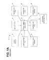
- FIG. 1A is a block diagram of a static timing analyzer system 2 , as is known in the prior art. Specifically, some examples of system 2 are marketed under the name Primetime® and Pathmill®. FIG. 1A illustrates the informational flow in a system 2 . At the center of the diagram is a static timing analyzer 10 , (i.e., the Primetime® program). Surrounding this block 10 are a number of other blocks that represent various input and output files and/or information.
- the static timing analyzer 10 may utilize a configuration file 12 , a file of timing models 14 , one or more netlist files 16 , a technology file 18 , and a parasitics file 20 , for various input information.
- the static timing analyzer 10 may generate a number of different output files or other output information, including a critical path report 22 , a runtime log file 24 , an error report 26 , and a software interface file 28 .
- the static timing analyzer 10 When started, the static timing analyzer 10 first processes the input netlist file(s) 16 , the technology file 18 , and the configuration files 12 . The information from these files is subsequently used for performing path analyses.
- the function and operation of the static timing analyzer 10 are generally well known, and therefore need not be discussed in detail herein.
- timing analyzer 10 While tools such as these are useful for the design verification process after layout, there are various shortcomings in the static timing analyzer 10 , and other similar products. These shortcomings include, but are not limited to, performing accurate clock gating checks on logic cells during static timing. Problems with clock gating occur when a logic cell is used to turn a clock on or off based upon other logic signals. One problem occurs when the clock signal changes state at or near the same time that the logic signal changes state as to create what is referred to as a timing “glitch.” These timing glitches can cause erroneous circuit operations. The most common method for preventing glitches is a clock gating check. It is nearly impossible to perform a clock gating check manually in a large design because a large design may have tens of thousands of logic cells each requiring a clock gating check.
- the clock gating check ensures that the clock transition does not too closely precede or follow a change in the gating signal 43 .
- FIG. 1B where the clock signal 42 and gating signal 43 are input into logic cell 41 , and the output of logic cell 41 is the output signal 48 .
- the clock gating check makes sure that the transition of the clock signal 42 does not too closely precede or follow a transition in the gating signal 43 , thereby creating glitches on the output signal 48 .
- FIG. 1 C A comparison of these signals illustrating the potential problem is illustrated in FIG. 1 C.
- the clock signal 42 has a clock transition time 44 that is approximately equal to the gating signal transition time 46 of the gating signal 43 .
- This input of the clock signal 42 and the gating signal 43 into logic cell 41 can create an output signal 48 with a glitch 49 .
- Clock gating checks usually include a safety margin factor or buffer time period that is set at the time of the static timing analysis. This buffer time period 51 is illustrated in FIGS. 2A-2C. If the static timing engine calculates that the signals are far enough apart in time, then the clock gating check passes as illustrated in FIG. 2 A. As shown, the clock signal 42 transitions at clock transition time 44 and the buffer time period 51 expires prior to the gating signal transition time 46 of the gating signal 43 . In this scenario, the transition of clock signal 42 and gating signal 43 allows a sufficient time for the buffer time period 51 .
- a problem with the clock gating check occurs if the signals (i.e. the clock signal 42 and gating signal 43 ) have poor or slow transition times. However, if the clock transition time 44 of the clock signal 42 overlaps the gating signal transition time 46 of the gating signal 43 , then the clock gating check will also fail as shown in FIG. 2 B. In addition, there is a problem with the clock gating check of the prior art if the clock signal 42 and gating signal 43 have poor transition times that may be greater than the buffer time period 51 , but that still sufficiently overlap to cause glitches as illustrated in FIG. 2 C.
- the present invention provides a gating signal analysis system and method for performing accurate clock gating analysis on logic cells.
- the gating signal checker can be implemented as follows.
- the gating signal checker has logic that determines a clock transition time of a clock input into the logic cell, and logic that determines a transition time of at least one gating signal input into the logic cell.
- Also included in the gating signal checker system is logic that calculates a clock difference time between the clock transition time and the transition time of the at least one gating signal input into the logic cell, and logic that determines that the logic cell fails the clock gating check if the clock difference time is negative.
- the invention can also be viewed as providing one or more methods for performing accurate clock gating checks on logic cells.
- one such method can be summarized by the following steps: (1) determining a clock transition time of a clock input into the logic cell, (2) determining a transition time of at least one gating signal input into the logic cell, (3) calculating a clock difference time between the clock transition time and the transition time of the at least one gating signal input into the logic cell, and (4) determining that the logic cell passes the clock gating check if the clock difference time is positive.
- FIG. 1A is a block diagram of a static timing analyzer system, as is known in the prior art.
- FIG. 1B is an example of a clock gating cell, as known in the prior art.
- FIG. 1C is a block diagram illustrating the input signals that can cause a glitch in a logic cell, as known in the prior art.
- FIGS. 2A-2C are block diagrams illustrating the states that occur when performing a clock gating check, as is known in the prior art.
- FIG. 3 is a block diagram illustrating one possible implementation of a gating signal checker that utilizes a clock gating check calculation process, situated within a computer readable medium.
- FIG. 4 is a block diagram illustrating one possible implementation of the gating signal checker with the clock gating check calculation process of the present invention, as shown in FIG. 3 .
- FIG. 5 is a flowchart illustrating one possible implementation of the gating signal checker of the present invention, as shown in FIGS. 3 and 4.
- FIG. 6 is a flowchart illustrating one possible implementation of the method for performing the clock gating check calculation process as shown in FIGS. 3-5.
- FIG. 7A is a block diagram illustrating an example of a clock signal and gating signal that passed the gating signal check of the present invention as illustrated in FIGS. 3-6.
- FIG. 7B is a block diagram illustrating an example of a clock signal and gating signal failing the gating signal check of the present invention as illustrated in FIGS. 3-6.
- FIG. 7C is a block diagram illustrating one example of a clock signal and gating signal showing allowable signal overlap that passes the gating signal check of the present invention as shown in FIGS. 3-6.
- FIG. 7D is a block diagram illustrating one example of a clock signal and gating signal with an extra time buffer that passes the signal gating check of the present invention as illustrated in FIGS. 3-6.
- the gating signal checker of the present invention checks the real transition period of a logic cell for correct transition operation. This is superior to previous methods in that it does not require a pre-calculation of a safety margin that is to be used. In another embodiment, the gating signal checker of the present invention also allows for significantly different transition periods between the clock and gating signals, and even between the individual gating signals if there is more than one.
- the gating signal checker of the present invention operates by determining the signal transition times in reference to a clock, and determining the transition times of all of the gating signals for one gating cell. Upon determining these signal transition times, the clock transition period can be determined. Each gating signal is compared to the clock signal for both set up and hold, both in transition period and in transition time. The transition time indicates the point at which the signal changes from one state to another. The transition period is the time period needed for a signal to completely transition from one state to another.
- Fractor E it is possible to have an allowable overlap percent (Factor E) that can be specified for each type of signal. This would allow overlap up to a percentage amount specified while still passing the clock signal check. If extra time is desired, the designer can also specify an extra buffer time period (Factor D) that would be included between the signals being tested.
- FIG. 3 is a block diagram illustrating one possible implementation of a gating signal checker 100 that utilizes the clock gating check calculation process 120 of the present invention, situated within a computer readable medium, such as, for example, a memory 63 in a general-purpose computer system 61 .
- a general-purpose computer system can identify, access, and process resources desired by a user.
- the computer system 61 includes a processor 62 , memory 63 , and one or more input devices and/or output (I/O) devices (or peripherals) that are communicatively coupled via a local interface 64 .
- the local interface 64 can be, for example but not limited to, one or more buses or other wired or wireless connections, as is known in the art.
- the local interface 64 may have additional elements, which are omitted for simplicity, such as controllers, buffers (caches), drivers, repeaters, and receivers, to enable communications. Further, the local interface 64 may include address, control, and/or data connections to enable appropriate communications among the aforementioned components.
- the processor 62 is a hardware device for executing software that can be stored in memory 63 .
- the processor 62 can be virtually any custom made or commercially available processor, a central processing unit (CPU) or an auxiliary processor among several processors associated with the computer system 61 , and a semiconductor based microprocessor (in the form of a microchip) or a macroprocessor.
- microprocessors examples include an 80 ⁇ 86 or Pentium series microprocessor from Intel Corporation, U.S.A., a PowerPC microprocessor from IBM, U.S.A., a Sparc microprocessor from Sun Microsystems, Inc, a PA-RISC series microprocessor from Hewlett-Packard Company, U.S.A., or a 68xxx series microprocessor from Motorola Corporation, U.S.A.
- the memory 63 can include any one or a combination of volatile memory elements (e.g., random access memory (RAM, such as DRAM, SRAM, etc.)) and nonvolatile memory elements (e.g., ROM, hard drive, tape, CDROM, etc.). Moreover, the memory 63 may incorporate electronic, magnetic, optical, and/or other types of storage media. Note that the memory 63 can have a distributed architecture, where various components are situated remote from one another, but can be accessed by the processor 62 .
- the software in memory 63 may include one or more separate programs, each of which comprises an ordered listing of executable instructions for implementing logical functions.
- the software in the memory 63 includes an operating system (not shown), configuration file 12 , file of timing models 14 , one or more netlist files 16 , technology file 18 , and a parasitics file 20 , containing various input information.
- the critical path report 22 , runtime log file 24 , error report 26 , software interface file 28 , and data file 32 output files or other output information are also situated in memory 63 .
- the gating signal checker 100 is used to perform clock gating checks herein defined in further detail with regard to FIGS. 4-6.
- a non-exhaustive list of examples of suitable commercially available operating systems is as follows: a Windows operating system from Microsoft Corporation, U.S.A., a Netware operating system available from Novell, Inc., U.S.A., an operating system available from IBM, Inc., U.S.A., any LINUX operating system available from many vendors or a UNIX operating system, which is available for purchase from many vendors, such as Hewlett-Packard Company, U.S.A., Sun Microsystems, Inc. and AT&T Corporation, U.S.A.
- the operating system essentially controls the execution of other computer programs, such as the checksum code operation mechanism, and provides scheduling, input-output control, file and data management, memory management, and communication control and related services.
- the gating signal checker 100 that utilizes the clock gating check calculation process 120 may be a source program, executable program (object code), script, or any other entity comprising a set of instructions to be performed.
- a source program then the program is usually translated via a compiler, assembler, interpreter, or the like, which may or may not be included within the memory 63 , so as to operate properly in connection with the O/S.
- the gating signal checker 100 that utilizes clock gating check calculation process 120 can be written as (a) an object oriented programming language, which has classes of data and methods, or (b) a procedure programming language, which has routines, subroutines, and/or functions, for example but not limited to, C, C++, Pascal, BASIC, FORTRAN, COBOL, Perl, TCL, Java, and Ada.
- the I/O devices may include input devices, for example but not limited to, a keyboard 66 , mouse 65 , scanner, microphone, etc. Furthermore, the I/O devices may also include output devices, for example but not limited to, a printer, display 67 , etc. Finally, the I/O devices may further include devices that communicate both inputs and outputs, for instance but not limited to, a modulator/demodulator (modem; for accessing another device, system, or network) 68 , a radio frequency (RF) or other transceiver, a telephonic interface, a bridge, a router, etc.
- modem for accessing another device, system, or network
- RF radio frequency
- the software in the memory 63 may further include a basic input output system (BIOS) (omitted for simplicity).
- BIOS is a set of essential software routines that initialize and test hardware at startup, start-up the O/S, and support the transfer of data among the hardware devices.
- the BIOS is stored in ROM so that the BIOS can be executed when the computer system 61 is activated.
- the processor 62 When the computer system 61 is in operation, the processor 62 is configured to execute software stored within the memory 63 , to communicate data to and from the memory 63 , and to generally control operations of the computer system 61 pursuant to the software.
- the gating signal checker 100 that utilizes the clock gating check calculation process 120 and the O/S are read, in whole or in part, by the processor 62 , perhaps buffered within the processor 62 , and then executed.
- the gating signal checker 100 that utilizes the clock gating check calculation process 120 can be implemented in hardware, software, firmware or a combination thereof.
- the gating signal checker 100 with the clock gating check calculation process 120 is implemented in software or firmware that is stored in a memory, such as the system memory 63 , and that is executed by a suitable instruction execution system, such as processor 62 .
- FIGS. 4-6 collectively comprise a block diagram and flow charts that illustrates the top-level functional operation of the gating signal checker 100 with the clock gating check calculation process 120 method in accordance with the preferred embodiment of the present invention.
- FIG. 4 is a block diagram illustrating one possible implementation of a gating signal checker 100 with the clock gating check calculation process 120 of the present invention, as shown in FIG. 3 .
- the configuration file(s) 12 contains information that informs the static timing analyzer 10 how to perform its analysis, and various numbers of configuration files may be used.
- the netlist file 16 defines the various integrated circuit components, and their inter-relations.
- the static timing analyzer 10 may make available to the gating signal checker 100 a data file output 32 .
- the static timing analyzer 10 typically uses a netlist (i.e. a Verilog® netlist), extracted parasitics and design constraints used for common representation of a hardware device. The static timing analyzer then loads the netlist design and parasitics into the system for representation of the hardware device. The design constraints are applied to the representation of the hardware device and a static timing run is then performed.
- a netlist i.e. a Verilog® netlist
- Verilog® netlist Verilog® netlist
- the gating signal checker 100 preferably is configured to operate on an output of the static timing analyzer 10 .
- the static timing analyzer may be configured to generate output netlist files 16 , which the gating signal checker 100 utilizes as an input.
- a gating signal checker 100 may be desired.
- One such reason to utilize a gating signal checker 100 is to perform various checks over certain rules or strategies in an integrated circuit design. Such rules may vary from circuit to circuit, depending upon the particular application.
- the gating signal checker 100 of the preferred embodiment of the present invention operates to provide a method for determining the signal transition times in reference to the clock signal 42 (FIG. 1 B), and the transition time of all gating signals for one gating cell. Then, the clock signal transition period can be determined. Each gating signal is compared to the clock signal for both set-up and hold of the clock signal for both transition period and transition time. If the time between the gating signal and clock signal minus one-half the transition period of each signal is greater than or equal to zero, no transition overlap has occurred and the clock gating check passes. However, if the value after subtraction is less than zero, then the clock gating check fails.
- the gating signal checker 100 of the present invention is a stand-alone system and method that does not require additions to any operating static timing engine 10 currently being operated.
- the gating signal checker 100 of the present invention may be integrated into currently available static timing engines.
- FIG. 5 is a flowchart depicting one possible implementation of the gating signal checker 100 with the clock gating check calculation process 120 of the present invention.
- the gating signal checker 100 of the present invention checks the transition times of a logic cell or element for correct transition operation. This is superior to previous methods in that it does not require a pre-calculation of a safety margin that is to be used.
- the gating signal checker of the present invention also allows for significantly different transition periods between the clock and gating signals, and even between the individual gating signals if there is more than one.
- the gating signal checker 100 initializes step 101 .
- the maximum overlap percentage or minimum time period between signals is set by the designer.
- the gating signal checker 100 of the present invention gets the first or next gating cell in the timing run.
- the gating signal checker 100 finds the gating inputs of the current gating cell at step 104 .
- the gating signal checker 100 gets the transition time and the transition period of the gating signals for the gating inputs.
- the gating signal checker 100 gets the clock transition period and the clock transition time.
- the gating signal checker 100 calculates any extra buffer time necessary for proper operation.
- the gating signal checker performs the clock gating check calculation process 120 (FIG. 6 ).
- the clock gating check calculation process is herein defined in further detail with regard to FIG. 6 .
- the gating signal checker determines, at step 113 , if there are more gating cells to be processed. If it is determined at step 113 that there are more gating cells to be processed, then the gating signal checker 100 returns to repeat steps 103 through 113 . However, if it is determined at step 113 that there are no more gating cells to be processed, then the gating signal checker 100 exits at step 119 .
- FIG. 6 is a flowchart depicting one possible implementation of the clock gating check calculation process 120 utilized within the gating signal checker 100 , as shown in FIGS. 3-5.
- the clock gating check calculation process 120 calculates the difference in time between the clock transition time 44 (FIG. 1C) and the gating signal transition time 46 (FIG. 1 C). This enables the clock gating check calculation process 120 to determine if the logic cell passes the clock gating check.
- the clock gating check calculation process 120 initializes step 121 .
- the clock gating check calculation process 120 then calculates the difference in time between the clock transition time 44 and the gating signal transition time 46 . In some applications, these transition times may be relative to the clock cycle.
- one-half of the clock transition period and one-half of the gating signal transition period is subtracted from the difference calculated at step 122 above. One-half of these transition periods are used to ensure that these signals have completed their respective transitions in order for the clock gating check to be performed.
- the clock gating check calculation process 120 subtracts either the minimum buffer period needed between signals or the maximum overlap time allowed from the difference calculated at step 123 above.
- a designer may allow some maximum overlap time in the transition time of the signals being compared. However, allowing transition overlap increases the chances of glitches due to lagging transition times.
- a designer may incorporate a minimum buffer period between transition signals to ensure that the signals complete their transition and, therefore, that the design is in its most robust state. This minimum buffer period can optionally include an extra buffer time period.
- the clock gating check calculation process 120 determines the difference between the clock transition time and gating transition time, and determines if that signal difference is equal to zero or is positive. If the signal difference is positive, the designer is notified and can be assured that there is sufficient time between the transition period of the clock signal and the transition period of the gating signal. If the signal difference is zero, the designer is notified that there is just enough time between the transition period of the clock signal and the transition period of the gating signal. However, if it is determined that the signal difference is negative, then the designer is notified that the clock gating check, in reference to the clock gating signal and clock transition, is in violation of the parameters set forth prior to the execution of the clock gating check. Typically, the designer is notified of the clock gating check results by messages on display 67 (FIG. 3 ), however, it is understood that the notices generated can be compiled and output in a report on an optional printer device.
- the clock gating calculation process 120 sets the clock gating check to “fail” for the current gating cell and notifies the designer of the failure, at step 126 .
- the clock gating check calculation process 120 exits at step 129 .
- the clock gating check is set to “pass” for the current gating cell and notifies the designer of the success at step 127 .
- the clock gating check calculation process 120 exits at step 129 .
- each block represents a module, segment, or portion of code, which comprises one or more executable instructions for implementing the specified logical function(s).
- the functions noted in the blocks may occur out of the order shown. For example, two blocks shown in succession may in fact be executed substantially concurrently or the blocks may sometimes be executed in the reverse order, depending upon the functionality involved.
- the gating signal checker 100 of the present invention determines the clock transition time 44 in reference to the gating signal transition time 46 for one gating cell 41 (FIG. 1 B). Upon determining these signal transition times, the difference in the clock transition time 44 and gating signal transition time 46 can be determined. Each gating signal is compared to the clock signal 42 for both set-up and hold both in transition time period and in transition time. The transition time indicates the point at which the signal changes from one state to another, and the transition period is the period needed for a signal to completely transition from one state to another.
- pS pico seconds
Landscapes
- Engineering & Computer Science (AREA)
- Computer Hardware Design (AREA)
- Physics & Mathematics (AREA)
- Theoretical Computer Science (AREA)
- Evolutionary Computation (AREA)
- Geometry (AREA)
- General Engineering & Computer Science (AREA)
- General Physics & Mathematics (AREA)
- Design And Manufacture Of Integrated Circuits (AREA)
- Tests Of Electronic Circuits (AREA)
Abstract
Description

Claims (28)
Priority Applications (1)
| Application Number | Priority Date | Filing Date | Title |
|---|---|---|---|
| US10/163,391 US6807658B2 (en) | 2002-06-05 | 2002-06-05 | Systems and methods for performing clock gating checks |
Applications Claiming Priority (1)
| Application Number | Priority Date | Filing Date | Title |
|---|---|---|---|
| US10/163,391 US6807658B2 (en) | 2002-06-05 | 2002-06-05 | Systems and methods for performing clock gating checks |
Publications (2)
| Publication Number | Publication Date |
|---|---|
| US20030229870A1 US20030229870A1 (en) | 2003-12-11 |
| US6807658B2 true US6807658B2 (en) | 2004-10-19 |
Family
ID=29709960
Family Applications (1)
| Application Number | Title | Priority Date | Filing Date |
|---|---|---|---|
| US10/163,391 Expired - Lifetime US6807658B2 (en) | 2002-06-05 | 2002-06-05 | Systems and methods for performing clock gating checks |
Country Status (1)
| Country | Link |
|---|---|
| US (1) | US6807658B2 (en) |
Cited By (5)
| Publication number | Priority date | Publication date | Assignee | Title |
|---|---|---|---|---|
| US7269809B2 (en) * | 2004-06-23 | 2007-09-11 | Sioptical, Inc. | Integrated approach for design, simulation and verification of monolithic, silicon-based opto-electronic circuits |
| US7454730B1 (en) * | 2005-12-02 | 2008-11-18 | Sun Microsystems, Inc. | Repeater insertion for concurrent setup time and hold time violations |
| US20110066988A1 (en) * | 2009-09-17 | 2011-03-17 | International Business Machines Corporation | Method, System, Computer Program Product, and Data Processing Program for Verification of Logic Circuit Designs Using Dynamic Clock Gating |
| US20110204178A1 (en) * | 2010-02-24 | 2011-08-25 | Lockheed Martin Corporation | Spot leading target laser guidance for engaging moving targets |
| US9934342B1 (en) * | 2016-12-02 | 2018-04-03 | Nxp Usa, Inc. | Clock gating verification during RTL stage of integrated circuit design |
Citations (3)
| Publication number | Priority date | Publication date | Assignee | Title |
|---|---|---|---|---|
| US5371416A (en) * | 1993-04-05 | 1994-12-06 | Motorola, Inc. | Circuit and method of synchronizing clock signals |
| US5657239A (en) * | 1992-10-30 | 1997-08-12 | Digital Equipment Corporation | Timing verification using synchronizers and timing constraints |
| US20020087921A1 (en) * | 2000-12-29 | 2002-07-04 | Rodriguez Pablo M. | Method and apparatus for detecting and recovering from errors in a source synchronous bus |
-
2002
- 2002-06-05 US US10/163,391 patent/US6807658B2/en not_active Expired - Lifetime
Patent Citations (3)
| Publication number | Priority date | Publication date | Assignee | Title |
|---|---|---|---|---|
| US5657239A (en) * | 1992-10-30 | 1997-08-12 | Digital Equipment Corporation | Timing verification using synchronizers and timing constraints |
| US5371416A (en) * | 1993-04-05 | 1994-12-06 | Motorola, Inc. | Circuit and method of synchronizing clock signals |
| US20020087921A1 (en) * | 2000-12-29 | 2002-07-04 | Rodriguez Pablo M. | Method and apparatus for detecting and recovering from errors in a source synchronous bus |
Cited By (6)
| Publication number | Priority date | Publication date | Assignee | Title |
|---|---|---|---|---|
| US7269809B2 (en) * | 2004-06-23 | 2007-09-11 | Sioptical, Inc. | Integrated approach for design, simulation and verification of monolithic, silicon-based opto-electronic circuits |
| US7454730B1 (en) * | 2005-12-02 | 2008-11-18 | Sun Microsystems, Inc. | Repeater insertion for concurrent setup time and hold time violations |
| US20110066988A1 (en) * | 2009-09-17 | 2011-03-17 | International Business Machines Corporation | Method, System, Computer Program Product, and Data Processing Program for Verification of Logic Circuit Designs Using Dynamic Clock Gating |
| US8302043B2 (en) * | 2009-09-17 | 2012-10-30 | International Business Machines Corporation | Verification of logic circuit designs using dynamic clock gating |
| US20110204178A1 (en) * | 2010-02-24 | 2011-08-25 | Lockheed Martin Corporation | Spot leading target laser guidance for engaging moving targets |
| US9934342B1 (en) * | 2016-12-02 | 2018-04-03 | Nxp Usa, Inc. | Clock gating verification during RTL stage of integrated circuit design |
Also Published As
| Publication number | Publication date |
|---|---|
| US20030229870A1 (en) | 2003-12-11 |
Similar Documents
| Publication | Publication Date | Title |
|---|---|---|
| KR100846089B1 (en) | How to Distribute Multiple Glue Logic Elements Between Design Blocks and How to Increase Glue Logic Distribution Efficiency | |
| US6195629B1 (en) | Method and system for selectively disabling simulation model instrumentation | |
| US6954915B2 (en) | System and methods for pre-artwork signal-timing verification of an integrated circuit design | |
| CN117094269B (en) | Verification method, verification device, electronic equipment and readable storage medium | |
| CN117113907B (en) | Verification method, verification device, electronic equipment and readable storage medium | |
| US20040078175A1 (en) | Method and apparatus for modeling and simulating the effects of bridge defects in integrated circuits | |
| US6212491B1 (en) | Automatic adjustment for counting instrumentation | |
| US5966306A (en) | Method for verifying protocol conformance of an electrical interface | |
| US6910194B2 (en) | Systems and methods for timing a linear data path element during signal-timing verification of an integrated circuit design | |
| Simpson | FPGA design | |
| US6836874B2 (en) | Systems and methods for time-budgeting a complex hierarchical integrated circuit | |
| US7231627B2 (en) | Merging a hardware design language source file with a separate assertion file | |
| US6560571B1 (en) | Method and apparatus for prioritizing the order in which checks are performed on a node in an integrated circuit | |
| US6769101B2 (en) | Systems and methods providing scan-based delay test generation | |
| US6807658B2 (en) | Systems and methods for performing clock gating checks | |
| US6978406B2 (en) | System and method for testing memory arrays | |
| US6732343B2 (en) | System and methods for placing clock buffers in a datapath stack | |
| US6449578B1 (en) | Method and apparatus for determining the RC delays of a network of an integrated circuit | |
| US6735750B2 (en) | System and method for correcting charge collector violations | |
| US6983443B2 (en) | System and method for placing clock drivers in a standard cell block | |
| US6910193B1 (en) | System and method for executing tests on an integrated circuit design | |
| Kamath et al. | A comprehensive multi-voltage design platform for system-level validation of standard cell library | |
| Brinkmann et al. | Formal verification—the industrial perspective | |
| US6718522B1 (en) | Electrical rules checker system and method using tri-state logic for electrical rule checks | |
| US7447621B1 (en) | PLI-less co-simulation of ISS-based verification systems in hardware simulators |
Legal Events
| Date | Code | Title | Description |
|---|---|---|---|
| AS | Assignment |
Owner name: AGILENT TECHNOLOGIES, INC., COLORADO Free format text: ASSIGNMENT OF ASSIGNORS INTEREST;ASSIGNORS:MIELKE, DAVID JAMES;STONG, GAYVIN E.;REEL/FRAME:013981/0249 Effective date: 20020603 |
|
| STCF | Information on status: patent grant |
Free format text: PATENTED CASE |
|
| AS | Assignment |
Owner name: AVAGO TECHNOLOGIES GENERAL IP PTE. LTD., SINGAPORE Free format text: ASSIGNMENT OF ASSIGNORS INTEREST;ASSIGNOR:AGILENT TECHNOLOGIES, INC.;REEL/FRAME:017207/0020 Effective date: 20051201 |
|
| FPAY | Fee payment |
Year of fee payment: 4 |
|
| FPAY | Fee payment |
Year of fee payment: 8 |
|
| AS | Assignment |
Owner name: DEUTSCHE BANK AG NEW YORK BRANCH, AS COLLATERAL AGENT, NEW YORK Free format text: PATENT SECURITY AGREEMENT;ASSIGNOR:AVAGO TECHNOLOGIES GENERAL IP (SINGAPORE) PTE. LTD.;REEL/FRAME:032851/0001 Effective date: 20140506 Owner name: DEUTSCHE BANK AG NEW YORK BRANCH, AS COLLATERAL AG Free format text: PATENT SECURITY AGREEMENT;ASSIGNOR:AVAGO TECHNOLOGIES GENERAL IP (SINGAPORE) PTE. LTD.;REEL/FRAME:032851/0001 Effective date: 20140506 |
|
| AS | Assignment |
Owner name: AVAGO TECHNOLOGIES GENERAL IP (SINGAPORE) PTE. LTD., SINGAPORE Free format text: TERMINATION AND RELEASE OF SECURITY INTEREST IN PATENT RIGHTS (RELEASES RF 032851-0001);ASSIGNOR:DEUTSCHE BANK AG NEW YORK BRANCH, AS COLLATERAL AGENT;REEL/FRAME:037689/0001 Effective date: 20160201 Owner name: AVAGO TECHNOLOGIES GENERAL IP (SINGAPORE) PTE. LTD Free format text: TERMINATION AND RELEASE OF SECURITY INTEREST IN PATENT RIGHTS (RELEASES RF 032851-0001);ASSIGNOR:DEUTSCHE BANK AG NEW YORK BRANCH, AS COLLATERAL AGENT;REEL/FRAME:037689/0001 Effective date: 20160201 |
|
| AS | Assignment |
Owner name: BANK OF AMERICA, N.A., AS COLLATERAL AGENT, NORTH CAROLINA Free format text: PATENT SECURITY AGREEMENT;ASSIGNOR:AVAGO TECHNOLOGIES GENERAL IP (SINGAPORE) PTE. LTD.;REEL/FRAME:037808/0001 Effective date: 20160201 Owner name: BANK OF AMERICA, N.A., AS COLLATERAL AGENT, NORTH Free format text: PATENT SECURITY AGREEMENT;ASSIGNOR:AVAGO TECHNOLOGIES GENERAL IP (SINGAPORE) PTE. LTD.;REEL/FRAME:037808/0001 Effective date: 20160201 |
|
| FPAY | Fee payment |
Year of fee payment: 12 |
|
| AS | Assignment |
Owner name: AVAGO TECHNOLOGIES GENERAL IP (SINGAPORE) PTE. LTD Free format text: CORRECTIVE ASSIGNMENT TO CORRECT THE NAME OF THE ASSIGNEE PREVIOUSLY RECORDED ON REEL 017207 FRAME 0020. ASSIGNOR(S) HEREBY CONFIRMS THE ASSIGNMENT;ASSIGNOR:AGILENT TECHNOLOGIES, INC.;REEL/FRAME:038633/0001 Effective date: 20051201 |
|
| AS | Assignment |
Owner name: AVAGO TECHNOLOGIES GENERAL IP (SINGAPORE) PTE. LTD., SINGAPORE Free format text: TERMINATION AND RELEASE OF SECURITY INTEREST IN PATENTS;ASSIGNOR:BANK OF AMERICA, N.A., AS COLLATERAL AGENT;REEL/FRAME:041710/0001 Effective date: 20170119 Owner name: AVAGO TECHNOLOGIES GENERAL IP (SINGAPORE) PTE. LTD Free format text: TERMINATION AND RELEASE OF SECURITY INTEREST IN PATENTS;ASSIGNOR:BANK OF AMERICA, N.A., AS COLLATERAL AGENT;REEL/FRAME:041710/0001 Effective date: 20170119 |
|
| AS | Assignment |
Owner name: AVAGO TECHNOLOGIES INTERNATIONAL SALES PTE. LIMITE Free format text: MERGER;ASSIGNOR:AVAGO TECHNOLOGIES GENERAL IP (SINGAPORE) PTE. LTD.;REEL/FRAME:047196/0097 Effective date: 20180509 |
|
| AS | Assignment |
Owner name: AVAGO TECHNOLOGIES INTERNATIONAL SALES PTE. LIMITE Free format text: CORRECTIVE ASSIGNMENT TO CORRECT THE EXECUTION DATE PREVIOUSLY RECORDED AT REEL: 047196 FRAME: 0097. ASSIGNOR(S) HEREBY CONFIRMS THE MERGER;ASSIGNOR:AVAGO TECHNOLOGIES GENERAL IP (SINGAPORE) PTE. LTD.;REEL/FRAME:048555/0510 Effective date: 20180905 |
|
| AS | Assignment |
Owner name: BROADCOM INTERNATIONAL PTE. LTD., SINGAPORE Free format text: ASSIGNMENT OF ASSIGNORS INTEREST;ASSIGNOR:AVAGO TECHNOLOGIES INTERNATIONAL SALES PTE. LIMITED;REEL/FRAME:053771/0901 Effective date: 20200826 |