US6720642B1 - Flip chip in leaded molded package and method of manufacture thereof - Google Patents
Flip chip in leaded molded package and method of manufacture thereof Download PDFInfo
- Publication number
- US6720642B1 US6720642B1 US09/464,885 US46488599A US6720642B1 US 6720642 B1 US6720642 B1 US 6720642B1 US 46488599 A US46488599 A US 46488599A US 6720642 B1 US6720642 B1 US 6720642B1
- Authority
- US
- United States
- Prior art keywords
- semiconductor die
- die
- leadframe
- leads
- backside
- Prior art date
- Legal status (The legal status is an assumption and is not a legal conclusion. Google has not performed a legal analysis and makes no representation as to the accuracy of the status listed.)
- Expired - Lifetime
Links
Images


Classifications
-
- H10W70/481—
-
- H10W70/468—
-
- H10W74/114—
-
- H10W74/141—
-
- H10W46/00—
-
- H10W46/103—
-
- H10W46/401—
-
- H10W46/607—
Definitions
- the present invention relates to an improved package and method of packaging for a flip chip, and more particularly, to a flip chip wherein a die is attached to a leadframe that is then placed within a thinner package such that the back side of the die is exposed.
- power transistor packages those in the art are generally still using chip and wire bond interconnect technology. It is difficult to simplify the manufacturing process flow as all process steps, such as, for example, die attach, wire bond, and molding are required. As a result, there is a limit placed on the maximum size for the die. Thus, power transistor packages are suited for single die applications since formation of an isolated metal pad for power transistor packages that include multiple dies is very difficult.
- the present invention provides a chip device that includes a leadframe including a plurality of leads and a die coupled to the leadframe.
- the die includes a metallized back side as well as source and gate terminals opposite the metallized backside.
- the die is coupled to the leadframe such that the leads of the leadframe are directly coupled to the terminals.
- the chip device also includes a body including a window defined therein. The body is placed around at least a portion of the leadframe and the die such that the metallized back side of the die is adjacent the window.
- the die is coupled to the leadframe with solder bumps.
- the chip device includes two dies.
- a method of making a chip device includes providing a leadframe including a plurality of leads and a die attach pad and post, coupling a die to the die attach pad and post and, encapsulating at least a portion of the leadframe and die such that a metallized back side of the die is adjacent a window defined within the package mold.
- the method includes configuring leads of the leadframe.
- the configuring of the leads includes removing mold flashes and resins from the leads, removing dambars, and solder plating the leads.
- the leadframe is provided with preplated leads.
- the leadframe is provided with preplated leads and preformed leads.
- the leadframe is provided with two die attach pads and posts, wherein a first die is coupled to a first die attach pad and post, and a second die is coupled to a second die attach pad and post.
- the die is coupled to the leadframe die attach pad and post via solder bumps, wherein the solder bumps are re-flowed.
- the present invention provides a chip device that includes a thinner package, yet can accommodate a larger die. Indeed, up to a 70% increase in die area over wire bonded parts may be realized. Additionally, the present invention lends itself to packaging multiple dies in the same package. The present invention allows a die-to-die connection to be achieved using a low resistance path (leadframe based) capable of carrying high current. Furthermore, the present invention provides a simplified manufacturing process, especially in the embodiments where preplated and preformed leadframes are provided.
- FIG. 1A is a top plan view of a chip device in accordance with the present invention.
- FIG. 1B is a bottom elevation view of a chip device in accordance with the present invention.
- FIG. 1C is a sectional view of a chip device in accordance with the present invention as seen along the line A—A in FIG. 1A;
- FIG. 1D is a side elevation view of a chip device in accordance with the present invention.
- FIG. 2 is a top plan view of a leadframe for use in making a chip device in accordance with the present invention
- FIG. 3 a top plan view of an alternative leadframe for use in making a chip device in accordance with the present invention
- FIG. 3A is a top plan view of the leadframe illustrated in FIG. 3 a common die attach pad for two dies,
- FIG. 4 is a top plan view of a die for use in making a chip device in accordance with the present invention.
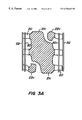
- FIG. 5 is a bottom plan view of a die coupled to a leadframe and encapsulated with a mold compound
- FIG. 6 is a top plan view of a old compound encapsulating a die coupled to a leadframe with dambars removed and marking on the mold compound;
- FIG. 7A is a top plan view of a preplated and preformed leadframe in accordance for making a chip device in accordance with an alternative embodiment of the present invention.
- FIG. 7B is a sectional view of the leadframe illustrated in FIG. 7A as seen along the line A—A.
- FIG. 8 is an exploded view of a leadframe and a die according to the present invention showing the leadframe connected to the die's terminals with solder bumps;
- FIG. 9 is a bottom plan view of two die coupled to a leadframe encapsulated with a mold compound according to the present invention.
- a chip device or semiconductor device 10 includes a leadframe 11 , a chip or die 12 and a mold compound or body 13 .
- backside 14 of the die is metallized.
- FIG. 2 illustrates a leadframe 11 a including a plurality of leads 20 and a die attach pad 21 a and post 22 a .
- the leadframe consists of a copper base and is either silver plated or nickel plated on the die attach pad and post.
- FIG. 3 illustrates a leadframe 11 b similar to leadframe 11 a .
- Leadframe 11 b includes two die attach pads and posts 22 b and thus is used for a chip device that includes two chips or dies. Thus, chip devices with multiple dies may be made.
- FIG. 3 illustrates two die attach pads, it should be readily apparent to those skilled in the art that leadframes with more than two die attach pads may be used, and hence, chip devices with more than two dies may be made.
- FIG. 3A illustrates leadframe 11 c that includes a common die attach pad 21 c for two dies thus providing a die-to-die connection.
- a leadframe to couple two dies, a low resistance path capable of carrying high current is achieved.
- this allows bi-directional switches to be fabricated (common source contact).
- FIG. 4 illustrates a die or chip 12 .
- back surface 14 of the die is preferably back metallized.
- top surface 30 of the die is passivated and includes a plurality of solder bumps 31 .
- solder bumps 31 Most of the solder bumps will serve to connect source region 32 of the chip to leads of the leadframe.
- Solder bump 33 serves as a gate bump and thus couples gate region 34 of the chip to a gate lead of the leadframe via die attach post 22 .
- FIG. 8 shows an exploded view of a leadframe 11 d , without the dambars and rails, coupled to the die 12 of FIG. 4 .
- the solder bumps of the source region 31 are coupled with the die attach pad 21 d .
- the solder bump of the gate region 33 is coupled to the post 22 d.
- the solder is reflowed, preferably with heat, in order to attach the chip to the leadframe and to provide good contact between the chip and the leadframe.
- the chip device is encapsulated with mold compound 13 such that the chip and the die attach pad and post are enveloped by the mold compound.
- mold compound 13 includes a window 40 defined therein.
- the chip device is encapsulated by the mold compound such that metallized back surface 14 of the die is adjacent to the window.
- metallized back surface 14 is at least partially within window 40 such that back surface 14 is substantially flush with back surface 41 of mold compound 13 .
- the metallized back surface of the die is exposed through the window.
- this exposed back surface of the die serves as the drain terminal of the chip device.
- FIG. 9 illustrates an alternative embodiment of the present invention wherein multiple die are packaged. Two die are arranged side by side such that their respective gate and source regions, not shown, may be contacted by the same leadframe, such as that pictured in FIG. 3 . After reflowing the solder connections, the device is encapsulated with mold compound 13 such that the metallized back surfaces of the die 14 a and 14 b are at least partially within their respective windows 40 a and 40 b such that the back surfaces 14 a and 14 b are substantially flush with the back surface 41 of the mold compound 13 . After being encapsulated, the metallized back surfaces of the die are exposed through the windows so that they may serve as the drain terminals of the device.
- the “package” of the chip device is essentially complete. Dambars 50 are removed and the leads are cleansed of any mold flashes and resins that may have accumulated during the manufacturing process. If desired, top surface 51 of the mold compound opposite the surface that includes the window may be marked with a laser or ink as shown in FIG. 6, for example, to identify the chip device. The leads are then solder plated and rails 52 at the end of the leads are removed. The leads are then configured by bending or forming them so that the chip may be placed on a circuit board. As can be seen in FIG. 1C, the leads are configured so that the ends are essentially co-planer with the exposed back surface 14 of the die.
- the leadframe is pre-plated prior to the start of the manufacturing process.
- the leadframe is pre-plated with NiPd.
- the manufacturing process proceeds as described above except the step of solder plating the leads is no longer required.
- the leads of the leadframe are “pre-formed.”
- the leadframe is plated with NiPd and the leads of the leadframe are pre-formed and configured, as can be seen in FIGS. 7A and 7B.
- the manufacturing process will proceed as outlined above, but the steps of plating the leads with solder and configuring the leads is no longer required.
- the manufacturing process may be simplified and shortened. This allows for a quicker, more efficient and less expensive manufacturing process to be realized.
- Die 12 may be manufactured in a conventional manner generally known in the art for a number of applications.
- the present invention provides a chip device that includes a thinner package, that can accommodate a larger die by using a single leadframe and using the back metallized surface of the die as drain contacts. Indeed, up to a 70% increase in die area over wire-bonded parts may be realized. Furthermore, the present invention provides a simplified manufacturing process, especially in the embodiments where pre-plated and pre-formed leadframes are provided.
Landscapes
- Lead Frames For Integrated Circuits (AREA)
- Structures Or Materials For Encapsulating Or Coating Semiconductor Devices Or Solid State Devices (AREA)
- Wire Bonding (AREA)
Abstract
Description
Claims (7)
Priority Applications (8)
| Application Number | Priority Date | Filing Date | Title |
|---|---|---|---|
| US09/464,885 US6720642B1 (en) | 1999-12-16 | 1999-12-16 | Flip chip in leaded molded package and method of manufacture thereof |
| JP2000381293A JP2001203310A (en) | 1999-12-16 | 2000-12-15 | Flip chip in leaded molded package and method of making same |
| DE10062542A DE10062542A1 (en) | 1999-12-16 | 2000-12-15 | Semiconductor chip arrangement for flip chip; has base plate metallized rear surface and source and gate contacts connected to contacts of connection frame and has casing with window near rear surface |
| TW089126928A TW473966B (en) | 1999-12-16 | 2000-12-15 | Flip chip in leaded molded package and method of manufacture thereof |
| US10/607,633 US6949410B2 (en) | 1999-12-16 | 2003-06-27 | Flip chip in leaded molded package and method of manufacture thereof |
| US10/702,792 US7154168B2 (en) | 1999-12-16 | 2003-11-05 | Flip chip in leaded molded package and method of manufacture thereof |
| US11/213,182 US7215011B2 (en) | 1999-12-16 | 2005-08-25 | Flip chip in leaded molded package and method of manufacture thereof |
| US11/693,141 US7582956B2 (en) | 1999-12-16 | 2007-03-29 | Flip chip in leaded molded package and method of manufacture thereof |
Applications Claiming Priority (1)
| Application Number | Priority Date | Filing Date | Title |
|---|---|---|---|
| US09/464,885 US6720642B1 (en) | 1999-12-16 | 1999-12-16 | Flip chip in leaded molded package and method of manufacture thereof |
Related Child Applications (2)
| Application Number | Title | Priority Date | Filing Date |
|---|---|---|---|
| US10/607,633 Division US6949410B2 (en) | 1999-12-16 | 2003-06-27 | Flip chip in leaded molded package and method of manufacture thereof |
| US10/702,792 Continuation US7154168B2 (en) | 1999-12-16 | 2003-11-05 | Flip chip in leaded molded package and method of manufacture thereof |
Publications (1)
| Publication Number | Publication Date |
|---|---|
| US6720642B1 true US6720642B1 (en) | 2004-04-13 |
Family
ID=23845652
Family Applications (5)
| Application Number | Title | Priority Date | Filing Date |
|---|---|---|---|
| US09/464,885 Expired - Lifetime US6720642B1 (en) | 1999-12-16 | 1999-12-16 | Flip chip in leaded molded package and method of manufacture thereof |
| US10/607,633 Expired - Lifetime US6949410B2 (en) | 1999-12-16 | 2003-06-27 | Flip chip in leaded molded package and method of manufacture thereof |
| US10/702,792 Expired - Lifetime US7154168B2 (en) | 1999-12-16 | 2003-11-05 | Flip chip in leaded molded package and method of manufacture thereof |
| US11/213,182 Expired - Lifetime US7215011B2 (en) | 1999-12-16 | 2005-08-25 | Flip chip in leaded molded package and method of manufacture thereof |
| US11/693,141 Expired - Fee Related US7582956B2 (en) | 1999-12-16 | 2007-03-29 | Flip chip in leaded molded package and method of manufacture thereof |
Family Applications After (4)
| Application Number | Title | Priority Date | Filing Date |
|---|---|---|---|
| US10/607,633 Expired - Lifetime US6949410B2 (en) | 1999-12-16 | 2003-06-27 | Flip chip in leaded molded package and method of manufacture thereof |
| US10/702,792 Expired - Lifetime US7154168B2 (en) | 1999-12-16 | 2003-11-05 | Flip chip in leaded molded package and method of manufacture thereof |
| US11/213,182 Expired - Lifetime US7215011B2 (en) | 1999-12-16 | 2005-08-25 | Flip chip in leaded molded package and method of manufacture thereof |
| US11/693,141 Expired - Fee Related US7582956B2 (en) | 1999-12-16 | 2007-03-29 | Flip chip in leaded molded package and method of manufacture thereof |
Country Status (4)
| Country | Link |
|---|---|
| US (5) | US6720642B1 (en) |
| JP (1) | JP2001203310A (en) |
| DE (1) | DE10062542A1 (en) |
| TW (1) | TW473966B (en) |
Cited By (59)
| Publication number | Priority date | Publication date | Assignee | Title |
|---|---|---|---|---|
| US20030052408A1 (en) * | 2000-04-13 | 2003-03-20 | Fairchild Semiconductor Corporation | Semiconductor device including molded wireless exposed drain packaging |
| US20030193080A1 (en) * | 2002-04-16 | 2003-10-16 | Cabahug Elsie Agdon | Robust leaded molded packages and methods for forming the same |
| US20040056364A1 (en) * | 1999-12-16 | 2004-03-25 | Fairchild Semiconductor Corporation | Flip chip in leaded molded package and method of manufacture thereof |
| US20040157372A1 (en) * | 2003-02-11 | 2004-08-12 | Manatad Romel N. | Alternative flip chip in leaded molded package design and method for manufacture |
| US20040201086A1 (en) * | 2000-12-04 | 2004-10-14 | Fairchild Semiconductor Corporation | Flip chip in leaded molded package with two dies |
| US20040219887A1 (en) * | 1999-12-06 | 2004-11-04 | Conexant Systems, Inc. | Surface acoustic wave filter packaging |
| US20040241977A1 (en) * | 2000-12-04 | 2004-12-02 | Fairchild Semiconductor Corporation | Passivation scheme for bumped wafers |
| US20050001293A1 (en) * | 2001-03-12 | 2005-01-06 | Fairchild Semiconductor Corporation | Method for forming semiconductor device including stacked dies |
| WO2004032198A3 (en) * | 2002-10-03 | 2005-01-27 | Fairchild Semiconductor | Method for maintaining solder thickness in flipchip attach packaging processes |
| US20050051878A1 (en) * | 2000-07-19 | 2005-03-10 | Fairchild Semiconductor Corporation | Flip chip substrate design |
| US6870254B1 (en) | 2000-04-13 | 2005-03-22 | Fairchild Semiconductor Corporation | Flip clip attach and copper clip attach on MOSFET device |
| US20050218300A1 (en) * | 2004-04-02 | 2005-10-06 | Quinones Maria Clemens Y | Surface mount multi-channel optocoupler |
| US20060151861A1 (en) * | 2005-01-13 | 2006-07-13 | Noquil Jonathan A | Method to manufacture a universal footprint for a package with exposed chip |
| US20070001278A1 (en) * | 2005-06-30 | 2007-01-04 | Oseob Jeon | Semiconductor die package and method for making the same |
| US20070045785A1 (en) * | 2005-08-30 | 2007-03-01 | Noquil Jonathan A | Reversible-multiple footprint package and method of manufacturing |
| US20070114352A1 (en) * | 2005-11-18 | 2007-05-24 | Victor R Cruz Erwin | Semiconductor die package using leadframe and clip and method of manufacturing |
| US20070155058A1 (en) * | 2006-01-05 | 2007-07-05 | Jereza Armand Vincent C | Clipless and wireless semiconductor die package and method for making the same |
| US20070164428A1 (en) * | 2006-01-18 | 2007-07-19 | Alan Elbanhawy | High power module with open frame package |
| US20070181982A1 (en) * | 2006-02-04 | 2007-08-09 | Stats Chippac Ltd. | Integrated circuit package system with leadfinger support |
| US20070187807A1 (en) * | 2006-02-13 | 2007-08-16 | Jeongil Lee | Multi-chip module for battery power control |
| US20070200250A1 (en) * | 2004-08-24 | 2007-08-30 | Infineon Technologies Ag | Semiconductor Device with a Semiconductor Chip Using Lead Technology and Method of Manufacturing the Same |
| US20070235886A1 (en) * | 2006-04-06 | 2007-10-11 | Hamza Yilmaz | Semiconductor die packages using thin dies and metal substrates |
| US20070249092A1 (en) * | 2006-04-24 | 2007-10-25 | Rajeev Joshi | Semiconductor die package including multiple dies and a common node structure |
| US20080001279A1 (en) * | 2006-06-30 | 2008-01-03 | Alan Elbanhawy | Chip module for complete power train |
| US20080054417A1 (en) * | 2006-08-29 | 2008-03-06 | Sangdo Lee | Semiconductor die package including stacked dice and heat sink structures |
| US20080173991A1 (en) * | 2007-01-24 | 2008-07-24 | Erwin Victor Cruz | Pre-molded clip structure |
| US20080185696A1 (en) * | 2007-02-05 | 2008-08-07 | Ruben Madrid | Semiconductor die package including leadframe with die attach pad with folded edge |
| US20080209511A1 (en) * | 2004-05-18 | 2008-08-28 | Silverbrook Research Pty Ltd | Authentication method for pharmaceutical products having coded packaging |
| US20080203559A1 (en) * | 2007-02-28 | 2008-08-28 | Lee Keun-Hyuk | Power device package and semiconductor package mold for fabricating the same |
| US20080224285A1 (en) * | 2007-03-12 | 2008-09-18 | Lim Seung-Won | Power module having stacked flip-chip and method of fabricating the power module |
| US20080251739A1 (en) * | 2007-04-13 | 2008-10-16 | Yoon Hwa Choi | Optical coupler package |
| US20080258272A1 (en) * | 2007-04-19 | 2008-10-23 | Lay Yeap Lim | Etched leadframe structure |
| US20090008775A1 (en) * | 2007-07-05 | 2009-01-08 | Nec Electronics Corporation | Semiconductor device with welded leads and method of manufacturing the same |
| US20090057854A1 (en) * | 2007-08-28 | 2009-03-05 | Gomez Jocel P | Self locking and aligning clip structure for semiconductor die package |
| US20090057855A1 (en) * | 2007-08-30 | 2009-03-05 | Maria Clemens Quinones | Semiconductor die package including stand off structures |
| US20090057852A1 (en) * | 2007-08-27 | 2009-03-05 | Madrid Ruben P | Thermally enhanced thin semiconductor package |
| US20090140266A1 (en) * | 2007-11-30 | 2009-06-04 | Yong Liu | Package including oriented devices |
| US20090140179A1 (en) * | 2007-11-30 | 2009-06-04 | Yong Liu | Semiconductor die packages suitable for optoelectronic applications having clip attach structures for angled mounting of dice |
| US20090160036A1 (en) * | 2007-12-19 | 2009-06-25 | David Grey | Package with multiple dies |
| US20090174048A1 (en) * | 2008-01-09 | 2009-07-09 | Yong Liu | Die package including substrate with molded device |
| US20090174044A1 (en) * | 2007-12-13 | 2009-07-09 | Eom Joo-Yang | Multi-chip package |
| US20090179313A1 (en) * | 2008-01-10 | 2009-07-16 | Maria Clemens Quinones | Flex clip connector for semiconductor device |
| US20090194856A1 (en) * | 2008-02-06 | 2009-08-06 | Gomez Jocel P | Molded package assembly |
| US20090218666A1 (en) * | 2008-02-28 | 2009-09-03 | Yang Gwi-Gyeon | Power device package and method of fabricating the same |
| US20090230536A1 (en) * | 2008-03-12 | 2009-09-17 | Yong Liu | Semiconductor die package including multiple semiconductor dice |
| US20090243079A1 (en) * | 2008-03-31 | 2009-10-01 | Lim Seung-Won | Semiconductor device package |
| US20090278241A1 (en) * | 2008-05-08 | 2009-11-12 | Yong Liu | Semiconductor die package including die stacked on premolded substrate including die |
| US7737548B2 (en) | 2007-08-29 | 2010-06-15 | Fairchild Semiconductor Corporation | Semiconductor die package including heat sinks |
| US20100148346A1 (en) * | 2008-12-12 | 2010-06-17 | Quinones Maria Clemens Y | Semiconductor die package including low stress configuration |
| US7768108B2 (en) | 2008-03-12 | 2010-08-03 | Fairchild Semiconductor Corporation | Semiconductor die package including embedded flip chip |
| US20100193921A1 (en) * | 2009-02-05 | 2010-08-05 | Jereza Armand Vincent C | Semiconductor die package and method for making the same |
| US20100193803A1 (en) * | 2009-02-04 | 2010-08-05 | Yong Liu | Stacked Micro Optocouplers and Methods of Making the Same |
| US7791084B2 (en) | 2008-01-09 | 2010-09-07 | Fairchild Semiconductor Corporation | Package with overlapping devices |
| US20110227205A1 (en) * | 2010-03-18 | 2011-09-22 | Jun Lu | Multi-layer lead frame package and method of fabrication |
| US20110227207A1 (en) * | 2010-03-18 | 2011-09-22 | Alpha And Omega Semiconductor Incorporated | Stacked dual chip package and method of fabrication |
| US8193618B2 (en) | 2008-12-12 | 2012-06-05 | Fairchild Semiconductor Corporation | Semiconductor die package with clip interconnection |
| US8421204B2 (en) | 2011-05-18 | 2013-04-16 | Fairchild Semiconductor Corporation | Embedded semiconductor power modules and packages |
| US8436429B2 (en) | 2011-05-29 | 2013-05-07 | Alpha & Omega Semiconductor, Inc. | Stacked power semiconductor device using dual lead frame and manufacturing method |
| US9536800B2 (en) | 2013-12-07 | 2017-01-03 | Fairchild Semiconductor Corporation | Packaged semiconductor devices and methods of manufacturing |
Families Citing this family (17)
| Publication number | Priority date | Publication date | Assignee | Title |
|---|---|---|---|---|
| US6469384B2 (en) * | 2001-02-01 | 2002-10-22 | Fairchild Semiconductor Corporation | Unmolded package for a semiconductor device |
| US7084488B2 (en) | 2001-08-01 | 2006-08-01 | Fairchild Semiconductor Corporation | Packaged semiconductor device and method of manufacture using shaped die |
| US6891256B2 (en) * | 2001-10-22 | 2005-05-10 | Fairchild Semiconductor Corporation | Thin, thermally enhanced flip chip in a leaded molded package |
| US7061077B2 (en) | 2002-08-30 | 2006-06-13 | Fairchild Semiconductor Corporation | Substrate based unmolded package including lead frame structure and semiconductor die |
| DE10243699B4 (en) * | 2002-09-20 | 2005-01-05 | Festo Ag & Co. | Method for producing a microvalve |
| CN100390979C (en) * | 2002-10-03 | 2008-05-28 | 费尔奇尔德半导体公司 | Semiconductor packages, electronic devices and methods for their manufacture |
| US20090166826A1 (en) * | 2007-12-27 | 2009-07-02 | Janducayan Omar A | Lead frame die attach paddles with sloped walls and backside grooves suitable for leadless packages |
| JP2009170476A (en) * | 2008-01-11 | 2009-07-30 | Panasonic Corp | Semiconductor device and manufacturing method of semiconductor device |
| US7758029B2 (en) * | 2008-02-07 | 2010-07-20 | Seville Classics Inc. | Cutting board with replaceable cutting sheets |
| JP5822468B2 (en) | 2011-01-11 | 2015-11-24 | ローム株式会社 | Semiconductor device |
| JP6452313B2 (en) * | 2014-05-13 | 2019-01-16 | キヤノン株式会社 | COMMUNICATION DEVICE, ITS CONTROL METHOD, PROGRAM |
| US9922935B2 (en) | 2014-09-17 | 2018-03-20 | Samsung Electronics Co., Ltd. | Semiconductor package and method of fabricating the same |
| KR20160032958A (en) | 2014-09-17 | 2016-03-25 | 삼성전자주식회사 | Semiconductor package and method for fabricating the same |
| DE102015120396B8 (en) * | 2015-11-25 | 2025-04-10 | Infineon Technologies Austria Ag | Semiconductor chip package including sidewall marking |
| US20200194347A1 (en) * | 2018-12-18 | 2020-06-18 | Alpha And Omega Semiconductor (Cayman) Ltd. | Semiconductor package and method of making the same |
| JP7454530B2 (en) * | 2021-07-28 | 2024-03-22 | 株式会社三井ハイテック | metal parts |
| EP4270476A1 (en) * | 2022-04-29 | 2023-11-01 | Infineon Technologies Austria AG | Semiconductor package and method for marking a semiconductor package |
Citations (13)
| Publication number | Priority date | Publication date | Assignee | Title |
|---|---|---|---|---|
| JPH01134958A (en) | 1987-11-20 | 1989-05-26 | Hitachi Ltd | Semiconductor device |
| US5105536A (en) * | 1989-07-03 | 1992-04-21 | General Electric Company | Method of packaging a semiconductor chip in a low inductance package |
| US5250841A (en) | 1992-04-06 | 1993-10-05 | Motorola, Inc. | Semiconductor device with test-only leads |
| US5319242A (en) | 1992-03-18 | 1994-06-07 | Motorola, Inc. | Semiconductor package having an exposed die surface |
| US6198163B1 (en) | 1999-10-18 | 2001-03-06 | Amkor Technology, Inc. | Thin leadframe-type semiconductor package having heat sink with recess and exposed surface |
| US6215176B1 (en) * | 1999-05-04 | 2001-04-10 | Sitron Precision Co., Ltd. | Dual leadframe package |
| US6307755B1 (en) | 1999-05-27 | 2001-10-23 | Richard K. Williams | Surface mount semiconductor package, die-leadframe combination and leadframe therefor and method of mounting leadframes to surfaces of semiconductor die |
| US6384492B1 (en) | 1995-05-04 | 2002-05-07 | Spinel Llc | Power semiconductor packaging |
| US6399418B1 (en) | 2001-07-26 | 2002-06-04 | Amkor Technology, Inc. | Method for forming a reduced thickness packaged electronic device |
| US6448110B1 (en) | 1999-08-25 | 2002-09-10 | Vanguard International Semiconductor Corporation | Method for fabricating a dual-chip package and package formed |
| US6452278B1 (en) | 2000-06-30 | 2002-09-17 | Amkor Technology, Inc. | Low profile package for plural semiconductor dies |
| US20030025183A1 (en) | 2001-08-01 | 2003-02-06 | Fairchild Semiconductor Corporation | Packaged semiconductor device and method of manufacture using shaped die |
| US6628880B2 (en) | 2001-04-06 | 2003-09-30 | Windsor Communications, Inc. | Fiber optic cable splice enclosure |
Family Cites Families (33)
| Publication number | Priority date | Publication date | Assignee | Title |
|---|---|---|---|---|
| US4678358A (en) * | 1985-07-15 | 1987-07-07 | National Semiconductor Corporation | Glass compression seals using low temperature glass |
| JPH04503283A (en) | 1989-07-03 | 1992-06-11 | ゼネラル・エレクトリック・カンパニイ | Low inductance encapsulation package containing semiconductor chip |
| US5147821A (en) * | 1990-09-28 | 1992-09-15 | Motorola, Inc. | Method for making a thermally enhanced semiconductor device by holding a leadframe against a heatsink through vacuum suction in a molding operation |
| US5183724A (en) * | 1990-12-18 | 1993-02-02 | Amkor Electronics, Inc. | Method of producing a strip of lead frames for integrated circuit dies in a continuous system |
| NL195026C (en) * | 1992-04-22 | 2003-06-18 | Yamaha Corporation | Method for processing a frame of electrical conductors for a semiconductor element. |
| JP3230348B2 (en) * | 1993-09-06 | 2001-11-19 | ソニー株式会社 | Resin-sealed semiconductor device and method of manufacturing the same |
| US5523604A (en) * | 1994-05-13 | 1996-06-04 | International Rectifier Corporation | Amorphous silicon layer for top surface of semiconductor device |
| US5554569A (en) | 1994-06-06 | 1996-09-10 | Motorola, Inc. | Method and apparatus for improving interfacial adhesion between a polymer and a metal |
| US5789809A (en) * | 1995-08-22 | 1998-08-04 | National Semiconductor Corporation | Thermally enhanced micro-ball grid array package |
| US5637916A (en) * | 1996-02-02 | 1997-06-10 | National Semiconductor Corporation | Carrier based IC packaging arrangement |
| US5811879A (en) | 1996-06-26 | 1998-09-22 | Micron Technology, Inc. | Stacked leads-over-chip multi-chip module |
| US6018686A (en) * | 1997-10-31 | 2000-01-25 | Cypress Semiconductor Corp. | Electrically imprinting a semiconductor die with identifying information |
| US6249041B1 (en) * | 1998-06-02 | 2001-06-19 | Siliconix Incorporated | IC chip package with directly connected leads |
| US6423623B1 (en) | 1998-06-09 | 2002-07-23 | Fairchild Semiconductor Corporation | Low Resistance package for semiconductor devices |
| US6133634A (en) * | 1998-08-05 | 2000-10-17 | Fairchild Semiconductor Corporation | High performance flip chip package |
| JP3560488B2 (en) * | 1999-01-29 | 2004-09-02 | ユナイテッド マイクロエレクトロニクス コープ | Chip scale package for multichip |
| US6214640B1 (en) * | 1999-02-10 | 2001-04-10 | Tessera, Inc. | Method of manufacturing a plurality of semiconductor packages |
| US6429509B1 (en) * | 1999-05-03 | 2002-08-06 | United Microelectronics Corporation | Integrated circuit with improved interconnect structure and process for making same |
| US6388336B1 (en) | 1999-09-15 | 2002-05-14 | Texas Instruments Incorporated | Multichip semiconductor assembly |
| US6319755B1 (en) * | 1999-12-01 | 2001-11-20 | Amkor Technology, Inc. | Conductive strap attachment process that allows electrical connector between an integrated circuit die and leadframe |
| US6744124B1 (en) * | 1999-12-10 | 2004-06-01 | Siliconix Incorporated | Semiconductor die package including cup-shaped leadframe |
| US6720642B1 (en) * | 1999-12-16 | 2004-04-13 | Fairchild Semiconductor Corporation | Flip chip in leaded molded package and method of manufacture thereof |
| US6989588B2 (en) * | 2000-04-13 | 2006-01-24 | Fairchild Semiconductor Corporation | Semiconductor device including molded wireless exposed drain packaging |
| US6661082B1 (en) * | 2000-07-19 | 2003-12-09 | Fairchild Semiconductor Corporation | Flip chip substrate design |
| US6699728B2 (en) * | 2000-09-06 | 2004-03-02 | Osram Opto Semiconductors Gmbh | Patterning of electrodes in oled devices |
| US6798044B2 (en) * | 2000-12-04 | 2004-09-28 | Fairchild Semiconductor Corporation | Flip chip in leaded molded package with two dies |
| US6469384B2 (en) * | 2001-02-01 | 2002-10-22 | Fairchild Semiconductor Corporation | Unmolded package for a semiconductor device |
| US6683375B2 (en) * | 2001-06-15 | 2004-01-27 | Fairchild Semiconductor Corporation | Semiconductor die including conductive columns |
| US6528880B1 (en) * | 2001-06-25 | 2003-03-04 | Lovoltech Inc. | Semiconductor package for power JFET having copper plate for source and ribbon contact for gate |
| US6633030B2 (en) * | 2001-08-31 | 2003-10-14 | Fiarchild Semiconductor | Surface mountable optocoupler package |
| US6566749B1 (en) * | 2002-01-15 | 2003-05-20 | Fairchild Semiconductor Corporation | Semiconductor die package with improved thermal and electrical performance |
| JP2005520339A (en) * | 2002-03-12 | 2005-07-07 | フェアチャイルド セミコンダクター コーポレーション | Wafer level coated copper stud bump |
| US7256479B2 (en) * | 2005-01-13 | 2007-08-14 | Fairchild Semiconductor Corporation | Method to manufacture a universal footprint for a package with exposed chip |
-
1999
- 1999-12-16 US US09/464,885 patent/US6720642B1/en not_active Expired - Lifetime
-
2000
- 2000-12-15 DE DE10062542A patent/DE10062542A1/en not_active Withdrawn
- 2000-12-15 TW TW089126928A patent/TW473966B/en not_active IP Right Cessation
- 2000-12-15 JP JP2000381293A patent/JP2001203310A/en not_active Abandoned
-
2003
- 2003-06-27 US US10/607,633 patent/US6949410B2/en not_active Expired - Lifetime
- 2003-11-05 US US10/702,792 patent/US7154168B2/en not_active Expired - Lifetime
-
2005
- 2005-08-25 US US11/213,182 patent/US7215011B2/en not_active Expired - Lifetime
-
2007
- 2007-03-29 US US11/693,141 patent/US7582956B2/en not_active Expired - Fee Related
Patent Citations (13)
| Publication number | Priority date | Publication date | Assignee | Title |
|---|---|---|---|---|
| JPH01134958A (en) | 1987-11-20 | 1989-05-26 | Hitachi Ltd | Semiconductor device |
| US5105536A (en) * | 1989-07-03 | 1992-04-21 | General Electric Company | Method of packaging a semiconductor chip in a low inductance package |
| US5319242A (en) | 1992-03-18 | 1994-06-07 | Motorola, Inc. | Semiconductor package having an exposed die surface |
| US5250841A (en) | 1992-04-06 | 1993-10-05 | Motorola, Inc. | Semiconductor device with test-only leads |
| US6384492B1 (en) | 1995-05-04 | 2002-05-07 | Spinel Llc | Power semiconductor packaging |
| US6215176B1 (en) * | 1999-05-04 | 2001-04-10 | Sitron Precision Co., Ltd. | Dual leadframe package |
| US6307755B1 (en) | 1999-05-27 | 2001-10-23 | Richard K. Williams | Surface mount semiconductor package, die-leadframe combination and leadframe therefor and method of mounting leadframes to surfaces of semiconductor die |
| US6448110B1 (en) | 1999-08-25 | 2002-09-10 | Vanguard International Semiconductor Corporation | Method for fabricating a dual-chip package and package formed |
| US6198163B1 (en) | 1999-10-18 | 2001-03-06 | Amkor Technology, Inc. | Thin leadframe-type semiconductor package having heat sink with recess and exposed surface |
| US6452278B1 (en) | 2000-06-30 | 2002-09-17 | Amkor Technology, Inc. | Low profile package for plural semiconductor dies |
| US6628880B2 (en) | 2001-04-06 | 2003-09-30 | Windsor Communications, Inc. | Fiber optic cable splice enclosure |
| US6399418B1 (en) | 2001-07-26 | 2002-06-04 | Amkor Technology, Inc. | Method for forming a reduced thickness packaged electronic device |
| US20030025183A1 (en) | 2001-08-01 | 2003-02-06 | Fairchild Semiconductor Corporation | Packaged semiconductor device and method of manufacture using shaped die |
Cited By (137)
| Publication number | Priority date | Publication date | Assignee | Title |
|---|---|---|---|---|
| US20040219887A1 (en) * | 1999-12-06 | 2004-11-04 | Conexant Systems, Inc. | Surface acoustic wave filter packaging |
| US7016655B2 (en) * | 1999-12-06 | 2006-03-21 | Skyworks Solutions, Inc. | Surface acoustic wave filter packaging |
| US20040056364A1 (en) * | 1999-12-16 | 2004-03-25 | Fairchild Semiconductor Corporation | Flip chip in leaded molded package and method of manufacture thereof |
| US7154168B2 (en) | 1999-12-16 | 2006-12-26 | Fairchild Semiconductor Corporation | Flip chip in leaded molded package and method of manufacture thereof |
| US6949410B2 (en) | 1999-12-16 | 2005-09-27 | Fairchild Semiconductor Corporation | Flip chip in leaded molded package and method of manufacture thereof |
| US20050167848A1 (en) * | 1999-12-16 | 2005-08-04 | Fairchild Semiconductor Corporation | Filp chip in leaded molded package and method of manufacture thereof |
| US20050130350A1 (en) * | 2000-04-13 | 2005-06-16 | Estacio Maria Cristina B. | Flip clip attach and copper clip attach on MOSFET device |
| US20030052408A1 (en) * | 2000-04-13 | 2003-03-20 | Fairchild Semiconductor Corporation | Semiconductor device including molded wireless exposed drain packaging |
| US6989588B2 (en) | 2000-04-13 | 2006-01-24 | Fairchild Semiconductor Corporation | Semiconductor device including molded wireless exposed drain packaging |
| US7052938B2 (en) | 2000-04-13 | 2006-05-30 | Fairchild Semiconductor Corporation | Flip clip attach and copper clip attach on MOSFET device |
| US6870254B1 (en) | 2000-04-13 | 2005-03-22 | Fairchild Semiconductor Corporation | Flip clip attach and copper clip attach on MOSFET device |
| US7101734B2 (en) | 2000-07-19 | 2006-09-05 | Fairchild Semiconductor Corporation | Flip chip substrate design |
| US20050051878A1 (en) * | 2000-07-19 | 2005-03-10 | Fairchild Semiconductor Corporation | Flip chip substrate design |
| US20040241977A1 (en) * | 2000-12-04 | 2004-12-02 | Fairchild Semiconductor Corporation | Passivation scheme for bumped wafers |
| US7029947B2 (en) | 2000-12-04 | 2006-04-18 | Fairchild Semiconductor Corporation | Flip chip in leaded molded package with two dies |
| US20040201086A1 (en) * | 2000-12-04 | 2004-10-14 | Fairchild Semiconductor Corporation | Flip chip in leaded molded package with two dies |
| US7008868B2 (en) | 2000-12-04 | 2006-03-07 | Fairchild Semiconductor Corporation | Passivation scheme for bumped wafers |
| US7071033B2 (en) * | 2001-03-12 | 2006-07-04 | Fairchild Semiconductor Corporation | Method for forming semiconductor device including stacked dies |
| US20050001293A1 (en) * | 2001-03-12 | 2005-01-06 | Fairchild Semiconductor Corporation | Method for forming semiconductor device including stacked dies |
| US20060231933A1 (en) * | 2002-04-16 | 2006-10-19 | Cabahug Elsie A | Robust leaded molded packages and methods for forming the same |
| US7122884B2 (en) * | 2002-04-16 | 2006-10-17 | Fairchild Semiconductor Corporation | Robust leaded molded packages and methods for forming the same |
| US20030193080A1 (en) * | 2002-04-16 | 2003-10-16 | Cabahug Elsie Agdon | Robust leaded molded packages and methods for forming the same |
| US7560311B2 (en) | 2002-04-16 | 2009-07-14 | Fairchild Semiconductor Corporation | Robust leaded molded packages and methods for forming the same |
| US6943434B2 (en) | 2002-10-03 | 2005-09-13 | Fairchild Semiconductor Corporation | Method for maintaining solder thickness in flipchip attach packaging processes |
| US20050224940A1 (en) * | 2002-10-03 | 2005-10-13 | Tangpuz Consuelo N | Method for maintaining solder thickness in flipchip attach packaging processes |
| WO2004032198A3 (en) * | 2002-10-03 | 2005-01-27 | Fairchild Semiconductor | Method for maintaining solder thickness in flipchip attach packaging processes |
| US20070241431A1 (en) * | 2003-02-11 | 2007-10-18 | Manatad Romel N | Alternative flip chip in leaded molded package design and method for manufacture |
| US7217594B2 (en) | 2003-02-11 | 2007-05-15 | Fairchild Semiconductor Corporation | Alternative flip chip in leaded molded package design and method for manufacture |
| US20040157372A1 (en) * | 2003-02-11 | 2004-08-12 | Manatad Romel N. | Alternative flip chip in leaded molded package design and method for manufacture |
| US7586178B2 (en) | 2003-02-11 | 2009-09-08 | Fairchild Semiconductor Corporation | Alternative flip chip in leaded molded package design and method for manufacture |
| US20050218300A1 (en) * | 2004-04-02 | 2005-10-06 | Quinones Maria Clemens Y | Surface mount multi-channel optocoupler |
| US7196313B2 (en) | 2004-04-02 | 2007-03-27 | Fairchild Semiconductor Corporation | Surface mount multi-channel optocoupler |
| US20080209511A1 (en) * | 2004-05-18 | 2008-08-28 | Silverbrook Research Pty Ltd | Authentication method for pharmaceutical products having coded packaging |
| US7656033B2 (en) * | 2004-08-24 | 2010-02-02 | Infineon Technologies Ag | Semiconductor device with a semiconductor chip using lead technology and method of manufacturing the same |
| US20070200250A1 (en) * | 2004-08-24 | 2007-08-30 | Infineon Technologies Ag | Semiconductor Device with a Semiconductor Chip Using Lead Technology and Method of Manufacturing the Same |
| US7256479B2 (en) | 2005-01-13 | 2007-08-14 | Fairchild Semiconductor Corporation | Method to manufacture a universal footprint for a package with exposed chip |
| WO2006076101A3 (en) * | 2005-01-13 | 2007-01-04 | Fairchild Semiconductor | A method to manufacture a universal footprint for a package with exposed chip |
| CN100539103C (en) * | 2005-01-13 | 2009-09-09 | 费查尔德半导体有限公司 | Semiconductor die package including uniform footprint and method of manufacturing the same |
| WO2006076143A3 (en) * | 2005-01-13 | 2006-09-14 | Fairchild Semiconductor | Semiconductor die package including universal footprint and method for manufacturing the same |
| US20060151861A1 (en) * | 2005-01-13 | 2006-07-13 | Noquil Jonathan A | Method to manufacture a universal footprint for a package with exposed chip |
| US20070001278A1 (en) * | 2005-06-30 | 2007-01-04 | Oseob Jeon | Semiconductor die package and method for making the same |
| US8664752B2 (en) | 2005-06-30 | 2014-03-04 | Fairchild Semiconductor Corporation | Semiconductor die package and method for making the same |
| US20100258925A1 (en) * | 2005-06-30 | 2010-10-14 | Oseob Jeon | Semiconductor die package and method for making the same |
| US8183088B2 (en) | 2005-06-30 | 2012-05-22 | Fairchild Semiconductor Corporation | Semiconductor die package and method for making the same |
| WO2007005263A3 (en) * | 2005-06-30 | 2007-04-19 | Fairchild Semiconductor | Semiconductor die package and method for making the same |
| US7772681B2 (en) | 2005-06-30 | 2010-08-10 | Fairchild Semiconductor Corporation | Semiconductor die package and method for making the same |
| WO2007027790A3 (en) * | 2005-08-30 | 2007-04-26 | Fairchild Semiconductor | Reversible-multiple footprint package and method of manufacturing |
| US20070045785A1 (en) * | 2005-08-30 | 2007-03-01 | Noquil Jonathan A | Reversible-multiple footprint package and method of manufacturing |
| US7285849B2 (en) | 2005-11-18 | 2007-10-23 | Fairchild Semiconductor Corporation | Semiconductor die package using leadframe and clip and method of manufacturing |
| US20080044946A1 (en) * | 2005-11-18 | 2008-02-21 | Cruz Erwin Victor R | Semiconductor die package using leadframe and clip and method of manufacturing |
| US8058107B2 (en) | 2005-11-18 | 2011-11-15 | Cruz Erwin Victor R | Semiconductor die package using leadframe and clip and method of manufacturing |
| US20070114352A1 (en) * | 2005-11-18 | 2007-05-24 | Victor R Cruz Erwin | Semiconductor die package using leadframe and clip and method of manufacturing |
| US7371616B2 (en) | 2006-01-05 | 2008-05-13 | Fairchild Semiconductor Corporation | Clipless and wireless semiconductor die package and method for making the same |
| US20070155058A1 (en) * | 2006-01-05 | 2007-07-05 | Jereza Armand Vincent C | Clipless and wireless semiconductor die package and method for making the same |
| US20070164428A1 (en) * | 2006-01-18 | 2007-07-19 | Alan Elbanhawy | High power module with open frame package |
| US20090179314A1 (en) * | 2006-02-04 | 2009-07-16 | Bathan Henry D | Integrated circuit package system with leadfinger support |
| US20070181982A1 (en) * | 2006-02-04 | 2007-08-09 | Stats Chippac Ltd. | Integrated circuit package system with leadfinger support |
| US8022514B2 (en) | 2006-02-04 | 2011-09-20 | Stats Chippac Ltd. | Integrated circuit package system with leadfinger support |
| US7541221B2 (en) | 2006-02-04 | 2009-06-02 | Stats Chippac Ltd. | Integrated circuit package system with leadfinger support |
| US7868432B2 (en) | 2006-02-13 | 2011-01-11 | Fairchild Semiconductor Corporation | Multi-chip module for battery power control |
| US20070187807A1 (en) * | 2006-02-13 | 2007-08-16 | Jeongil Lee | Multi-chip module for battery power control |
| US7768075B2 (en) | 2006-04-06 | 2010-08-03 | Fairchild Semiconductor Corporation | Semiconductor die packages using thin dies and metal substrates |
| US20070235886A1 (en) * | 2006-04-06 | 2007-10-11 | Hamza Yilmaz | Semiconductor die packages using thin dies and metal substrates |
| US7618896B2 (en) | 2006-04-24 | 2009-11-17 | Fairchild Semiconductor Corporation | Semiconductor die package including multiple dies and a common node structure |
| US8212361B2 (en) | 2006-04-24 | 2012-07-03 | Fairchild Semiconductor Corporation | Semiconductor die package including multiple dies and a common node structure |
| US20070249092A1 (en) * | 2006-04-24 | 2007-10-25 | Rajeev Joshi | Semiconductor die package including multiple dies and a common node structure |
| US7875498B2 (en) | 2006-06-30 | 2011-01-25 | Fairchild Semiconductor Corporation | Chip module for complete power train |
| US7656024B2 (en) | 2006-06-30 | 2010-02-02 | Fairchild Semiconductor Corporation | Chip module for complete power train |
| US20080001279A1 (en) * | 2006-06-30 | 2008-01-03 | Alan Elbanhawy | Chip module for complete power train |
| US20080054417A1 (en) * | 2006-08-29 | 2008-03-06 | Sangdo Lee | Semiconductor die package including stacked dice and heat sink structures |
| US7564124B2 (en) | 2006-08-29 | 2009-07-21 | Fairchild Semiconductor Corporation | Semiconductor die package including stacked dice and heat sink structures |
| US20100258923A1 (en) * | 2007-01-24 | 2010-10-14 | Erwin Victor Cruz | Pre-molded clip structure |
| US8513059B2 (en) | 2007-01-24 | 2013-08-20 | Fairchild Semiconductor Corporation | Pre-molded clip structure |
| US7838340B2 (en) | 2007-01-24 | 2010-11-23 | Fairchild Semiconductor Corporation | Pre-molded clip structure |
| US20080173991A1 (en) * | 2007-01-24 | 2008-07-24 | Erwin Victor Cruz | Pre-molded clip structure |
| US20100258924A1 (en) * | 2007-01-24 | 2010-10-14 | Erwin Victor Cruz | Pre-molded clip structure |
| US9583454B2 (en) | 2007-01-24 | 2017-02-28 | Fairchild Semiconductor Corporation | Semiconductor die package including low stress configuration |
| US7768105B2 (en) | 2007-01-24 | 2010-08-03 | Fairchild Semiconductor Corporation | Pre-molded clip structure |
| US8008759B2 (en) | 2007-01-24 | 2011-08-30 | Fairchild Semiconductor Corporation | Pre-molded clip structure |
| US20080185696A1 (en) * | 2007-02-05 | 2008-08-07 | Ruben Madrid | Semiconductor die package including leadframe with die attach pad with folded edge |
| US20110008935A1 (en) * | 2007-02-05 | 2011-01-13 | Fairchild Semiconductor Corporation | Semiconductor die package including leadframe with die attach pad with folded edge |
| US7821116B2 (en) | 2007-02-05 | 2010-10-26 | Fairchild Semiconductor Corporation | Semiconductor die package including leadframe with die attach pad with folded edge |
| US8258622B2 (en) | 2007-02-28 | 2012-09-04 | Fairchild Korea Semiconductor, Ltd. | Power device package and semiconductor package mold for fabricating the same |
| US20080203559A1 (en) * | 2007-02-28 | 2008-08-28 | Lee Keun-Hyuk | Power device package and semiconductor package mold for fabricating the same |
| US9130065B2 (en) | 2007-03-12 | 2015-09-08 | Fairchild Korea Semiconductor, Ltd | Power module having stacked flip-chip and method for fabricating the power module |
| US7675148B2 (en) | 2007-03-12 | 2010-03-09 | Fairchild Korea Semiconductor Ltd. | Power module having stacked flip-chip and method of fabricating the power module |
| US20080224285A1 (en) * | 2007-03-12 | 2008-09-18 | Lim Seung-Won | Power module having stacked flip-chip and method of fabricating the power module |
| US20080251739A1 (en) * | 2007-04-13 | 2008-10-16 | Yoon Hwa Choi | Optical coupler package |
| US7659531B2 (en) | 2007-04-13 | 2010-02-09 | Fairchild Semiconductor Corporation | Optical coupler package |
| US7683463B2 (en) | 2007-04-19 | 2010-03-23 | Fairchild Semiconductor Corporation | Etched leadframe structure including recesses |
| US20080258272A1 (en) * | 2007-04-19 | 2008-10-23 | Lay Yeap Lim | Etched leadframe structure |
| US8299620B2 (en) * | 2007-07-05 | 2012-10-30 | Renesas Electronics Corporation | Semiconductor device with welded leads and method of manufacturing the same |
| US20090008775A1 (en) * | 2007-07-05 | 2009-01-08 | Nec Electronics Corporation | Semiconductor device with welded leads and method of manufacturing the same |
| US20090057852A1 (en) * | 2007-08-27 | 2009-03-05 | Madrid Ruben P | Thermally enhanced thin semiconductor package |
| US7902657B2 (en) | 2007-08-28 | 2011-03-08 | Fairchild Semiconductor Corporation | Self locking and aligning clip structure for semiconductor die package |
| US20110076807A1 (en) * | 2007-08-28 | 2011-03-31 | Gomez Jocel P | Self locking and aligning clip structure for semiconductor die package |
| US8067273B2 (en) | 2007-08-28 | 2011-11-29 | Fairchild Semiconductor Corporation | Self locking and aligning clip structure for semiconductor die package |
| US20090057854A1 (en) * | 2007-08-28 | 2009-03-05 | Gomez Jocel P | Self locking and aligning clip structure for semiconductor die package |
| US7737548B2 (en) | 2007-08-29 | 2010-06-15 | Fairchild Semiconductor Corporation | Semiconductor die package including heat sinks |
| US20090057855A1 (en) * | 2007-08-30 | 2009-03-05 | Maria Clemens Quinones | Semiconductor die package including stand off structures |
| US7589338B2 (en) | 2007-11-30 | 2009-09-15 | Fairchild Semiconductor Corporation | Semiconductor die packages suitable for optoelectronic applications having clip attach structures for angled mounting of dice |
| US20090140266A1 (en) * | 2007-11-30 | 2009-06-04 | Yong Liu | Package including oriented devices |
| US20090140179A1 (en) * | 2007-11-30 | 2009-06-04 | Yong Liu | Semiconductor die packages suitable for optoelectronic applications having clip attach structures for angled mounting of dice |
| US7936054B2 (en) | 2007-12-13 | 2011-05-03 | Fairchild Korea Semiconductor Ltd. | Multi-chip package |
| US20090174044A1 (en) * | 2007-12-13 | 2009-07-09 | Eom Joo-Yang | Multi-chip package |
| US20090160036A1 (en) * | 2007-12-19 | 2009-06-25 | David Grey | Package with multiple dies |
| US7781872B2 (en) | 2007-12-19 | 2010-08-24 | Fairchild Semiconductor Corporation | Package with multiple dies |
| US7791084B2 (en) | 2008-01-09 | 2010-09-07 | Fairchild Semiconductor Corporation | Package with overlapping devices |
| US8106406B2 (en) | 2008-01-09 | 2012-01-31 | Fairchild Semiconductor Corporation | Die package including substrate with molded device |
| US20090174048A1 (en) * | 2008-01-09 | 2009-07-09 | Yong Liu | Die package including substrate with molded device |
| US8525192B2 (en) | 2008-01-09 | 2013-09-03 | Fairchild Semiconductor Corporation | Die package including substrate with molded device |
| US20090311832A1 (en) * | 2008-01-10 | 2009-12-17 | Quinones Maria Clemens Y | Flex Chip Connector For Semiconductor Device |
| US7626249B2 (en) | 2008-01-10 | 2009-12-01 | Fairchild Semiconductor Corporation | Flex clip connector for semiconductor device |
| US7824966B2 (en) | 2008-01-10 | 2010-11-02 | Fairchild Semiconductor Corporation | Flex chip connector for semiconductor device |
| US20090179313A1 (en) * | 2008-01-10 | 2009-07-16 | Maria Clemens Quinones | Flex clip connector for semiconductor device |
| US20090194856A1 (en) * | 2008-02-06 | 2009-08-06 | Gomez Jocel P | Molded package assembly |
| US8198139B2 (en) | 2008-02-28 | 2012-06-12 | Fairchild Korea Semiconductor Ltd. | Power device package and method of fabricating the same |
| US20090218666A1 (en) * | 2008-02-28 | 2009-09-03 | Yang Gwi-Gyeon | Power device package and method of fabricating the same |
| US7768108B2 (en) | 2008-03-12 | 2010-08-03 | Fairchild Semiconductor Corporation | Semiconductor die package including embedded flip chip |
| US20090230536A1 (en) * | 2008-03-12 | 2009-09-17 | Yong Liu | Semiconductor die package including multiple semiconductor dice |
| US8018054B2 (en) | 2008-03-12 | 2011-09-13 | Fairchild Semiconductor Corporation | Semiconductor die package including multiple semiconductor dice |
| US20090243079A1 (en) * | 2008-03-31 | 2009-10-01 | Lim Seung-Won | Semiconductor device package |
| US20090278241A1 (en) * | 2008-05-08 | 2009-11-12 | Yong Liu | Semiconductor die package including die stacked on premolded substrate including die |
| US20100148346A1 (en) * | 2008-12-12 | 2010-06-17 | Quinones Maria Clemens Y | Semiconductor die package including low stress configuration |
| US8193618B2 (en) | 2008-12-12 | 2012-06-05 | Fairchild Semiconductor Corporation | Semiconductor die package with clip interconnection |
| US8106501B2 (en) | 2008-12-12 | 2012-01-31 | Fairchild Semiconductor Corporation | Semiconductor die package including low stress configuration |
| US7973393B2 (en) | 2009-02-04 | 2011-07-05 | Fairchild Semiconductor Corporation | Stacked micro optocouplers and methods of making the same |
| US20100193803A1 (en) * | 2009-02-04 | 2010-08-05 | Yong Liu | Stacked Micro Optocouplers and Methods of Making the Same |
| US8222718B2 (en) | 2009-02-05 | 2012-07-17 | Fairchild Semiconductor Corporation | Semiconductor die package and method for making the same |
| US20100193921A1 (en) * | 2009-02-05 | 2010-08-05 | Jereza Armand Vincent C | Semiconductor die package and method for making the same |
| US8513784B2 (en) | 2010-03-18 | 2013-08-20 | Alpha & Omega Semiconductor Incorporated | Multi-layer lead frame package and method of fabrication |
| US20110227207A1 (en) * | 2010-03-18 | 2011-09-22 | Alpha And Omega Semiconductor Incorporated | Stacked dual chip package and method of fabrication |
| US8581376B2 (en) | 2010-03-18 | 2013-11-12 | Alpha & Omega Semiconductor Incorporated | Stacked dual chip package and method of fabrication |
| US20110227205A1 (en) * | 2010-03-18 | 2011-09-22 | Jun Lu | Multi-layer lead frame package and method of fabrication |
| US8421204B2 (en) | 2011-05-18 | 2013-04-16 | Fairchild Semiconductor Corporation | Embedded semiconductor power modules and packages |
| US8436429B2 (en) | 2011-05-29 | 2013-05-07 | Alpha & Omega Semiconductor, Inc. | Stacked power semiconductor device using dual lead frame and manufacturing method |
| US9536800B2 (en) | 2013-12-07 | 2017-01-03 | Fairchild Semiconductor Corporation | Packaged semiconductor devices and methods of manufacturing |
Also Published As
| Publication number | Publication date |
|---|---|
| TW473966B (en) | 2002-01-21 |
| US20050167848A1 (en) | 2005-08-04 |
| US7154168B2 (en) | 2006-12-26 |
| US20080036056A1 (en) | 2008-02-14 |
| JP2001203310A (en) | 2001-07-27 |
| US20040056364A1 (en) | 2004-03-25 |
| US7582956B2 (en) | 2009-09-01 |
| US20050280126A1 (en) | 2005-12-22 |
| US7215011B2 (en) | 2007-05-08 |
| DE10062542A1 (en) | 2001-06-21 |
| US6949410B2 (en) | 2005-09-27 |
Similar Documents
| Publication | Publication Date | Title |
|---|---|---|
| US6720642B1 (en) | Flip chip in leaded molded package and method of manufacture thereof | |
| US6849949B1 (en) | Thin stacked package | |
| US7781265B2 (en) | DFN semiconductor package having reduced electrical resistance | |
| US9589868B2 (en) | Packaging solutions for devices and systems comprising lateral GaN power transistors | |
| US7160760B2 (en) | Semiconductor device and a method of manufacturing the same | |
| JP2556294B2 (en) | Resin-sealed semiconductor device | |
| US7410834B2 (en) | Method of manufacturing a semiconductor device | |
| US6989588B2 (en) | Semiconductor device including molded wireless exposed drain packaging | |
| US7208818B2 (en) | Power semiconductor package | |
| US6756658B1 (en) | Making two lead surface mounting high power microleadframe semiconductor packages | |
| CN101073152B (en) | Electronic package and method with down-mounted pins | |
| US20040238923A1 (en) | Surface-mount-enhanced lead frame and method for fabricating semiconductor package with the same | |
| US7410835B2 (en) | Method for fabricating semiconductor package with short-prevented lead frame | |
| US6692991B2 (en) | Resin-encapsulated semiconductor device and method for manufacturing the same | |
| US20040036151A1 (en) | Double leadframe-based packaging structure and manufacturing process thereof | |
| KR100252862B1 (en) | Semiconductor package and method for fabricating the same | |
| KR100557976B1 (en) | Land grid array package and its manufacturing method |
Legal Events
| Date | Code | Title | Description |
|---|---|---|---|
| AS | Assignment |
Owner name: FAIRCHILD SEMICONDUCTOR CORPORATION, MAINE Free format text: ASSIGNMENT OF ASSIGNORS INTEREST;ASSIGNORS:JOSHI, RAJEEV;TANGPUZ, CONSUELO N.;MANATAD, ROMEL N.;REEL/FRAME:010732/0697;SIGNING DATES FROM 20000306 TO 20000310 |
|
| STCF | Information on status: patent grant |
Free format text: PATENTED CASE |
|
| FPAY | Fee payment |
Year of fee payment: 4 |
|
| REMI | Maintenance fee reminder mailed | ||
| FPAY | Fee payment |
Year of fee payment: 8 |
|
| FPAY | Fee payment |
Year of fee payment: 12 |
|
| AS | Assignment |
Owner name: DEUTSCHE BANK AG NEW YORK BRANCH, AS COLLATERAL AGENT, NEW YORK Free format text: PATENT SECURITY AGREEMENT;ASSIGNOR:FAIRCHILD SEMICONDUCTOR CORPORATION;REEL/FRAME:040075/0644 Effective date: 20160916 Owner name: DEUTSCHE BANK AG NEW YORK BRANCH, AS COLLATERAL AG Free format text: PATENT SECURITY AGREEMENT;ASSIGNOR:FAIRCHILD SEMICONDUCTOR CORPORATION;REEL/FRAME:040075/0644 Effective date: 20160916 |
|
| AS | Assignment |
Owner name: SEMICONDUCTOR COMPONENTS INDUSTRIES, LLC, ARIZONA Free format text: ASSIGNMENT OF ASSIGNORS INTEREST;ASSIGNOR:FAIRCHILD SEMICONDUCTOR CORPORATION;REEL/FRAME:057694/0374 Effective date: 20210722 Owner name: SEMICONDUCTOR COMPONENTS INDUSTRIES, LLC, ARIZONA Free format text: ASSIGNMENT OF ASSIGNOR'S INTEREST;ASSIGNOR:FAIRCHILD SEMICONDUCTOR CORPORATION;REEL/FRAME:057694/0374 Effective date: 20210722 |
|
| AS | Assignment |
Owner name: FAIRCHILD SEMICONDUCTOR CORPORATION, ARIZONA Free format text: RELEASE BY SECURED PARTY;ASSIGNOR:DEUTSCHE BANK AG NEW YORK BRANCH;REEL/FRAME:057969/0206 Effective date: 20211027 Owner name: FAIRCHILD SEMICONDUCTOR CORPORATION, ARIZONA Free format text: RELEASE OF SECURITY INTEREST;ASSIGNOR:DEUTSCHE BANK AG NEW YORK BRANCH;REEL/FRAME:057969/0206 Effective date: 20211027 |
|
| AS | Assignment |
Owner name: DEUTSCHE BANK AG NEW YORK BRANCH, AS COLLATERAL AGENT, NEW YORK Free format text: SECURITY INTEREST;ASSIGNOR:SEMICONDUCTOR COMPONENTS INDUSTRIES, LLC;REEL/FRAME:058871/0799 Effective date: 20211028 |
|
| AS | Assignment |
Owner name: FAIRCHILD SEMICONDUCTOR CORPORATION, ARIZONA Free format text: RELEASE OF SECURITY INTEREST IN PATENTS RECORDED AT REEL 040075, FRAME 0644;ASSIGNOR:DEUTSCHE BANK AG NEW YORK BRANCH, AS COLLATERAL AGENT;REEL/FRAME:064070/0536 Effective date: 20230622 Owner name: SEMICONDUCTOR COMPONENTS INDUSTRIES, LLC, ARIZONA Free format text: RELEASE OF SECURITY INTEREST IN PATENTS RECORDED AT REEL 040075, FRAME 0644;ASSIGNOR:DEUTSCHE BANK AG NEW YORK BRANCH, AS COLLATERAL AGENT;REEL/FRAME:064070/0536 Effective date: 20230622 |
|
| AS | Assignment |
Owner name: FAIRCHILD SEMICONDUCTOR CORPORATION, ARIZONA Free format text: RELEASE OF SECURITY INTEREST IN PATENTS RECORDED AT REEL 058871, FRAME 0799;ASSIGNOR:DEUTSCHE BANK AG NEW YORK BRANCH, AS COLLATERAL AGENT;REEL/FRAME:065653/0001 Effective date: 20230622 Owner name: SEMICONDUCTOR COMPONENTS INDUSTRIES, LLC, ARIZONA Free format text: RELEASE OF SECURITY INTEREST IN PATENTS RECORDED AT REEL 058871, FRAME 0799;ASSIGNOR:DEUTSCHE BANK AG NEW YORK BRANCH, AS COLLATERAL AGENT;REEL/FRAME:065653/0001 Effective date: 20230622 |