US6552398B2 - T-Ram array having a planar cell structure and method for fabricating the same - Google Patents
T-Ram array having a planar cell structure and method for fabricating the same Download PDFInfo
- Publication number
- US6552398B2 US6552398B2 US09/760,970 US76097001A US6552398B2 US 6552398 B2 US6552398 B2 US 6552398B2 US 76097001 A US76097001 A US 76097001A US 6552398 B2 US6552398 B2 US 6552398B2
- Authority
- US
- United States
- Prior art keywords
- ram
- cells
- array
- ram cells
- cell
- Prior art date
- Legal status (The legal status is an assumption and is not a legal conclusion. Google has not performed a legal analysis and makes no representation as to the accuracy of the status listed.)
- Expired - Fee Related
Links
- 238000000034 method Methods 0.000 title description 12
- 229910021420 polycrystalline silicon Inorganic materials 0.000 claims abstract description 28
- 229920005591 polysilicon Polymers 0.000 claims abstract description 28
- 239000004065 semiconductor Substances 0.000 claims abstract description 12
- 230000015654 memory Effects 0.000 claims description 12
- 125000006850 spacer group Chemical group 0.000 claims description 11
- 239000007943 implant Substances 0.000 abstract description 22
- 238000009792 diffusion process Methods 0.000 abstract description 6
- 239000012212 insulator Substances 0.000 abstract description 4
- 235000012431 wafers Nutrition 0.000 description 13
- 238000003491 array Methods 0.000 description 4
- 229910052785 arsenic Inorganic materials 0.000 description 3
- RQNWIZPPADIBDY-UHFFFAOYSA-N arsenic atom Chemical compound [As] RQNWIZPPADIBDY-UHFFFAOYSA-N 0.000 description 3
- 239000003989 dielectric material Substances 0.000 description 3
- 238000004519 manufacturing process Methods 0.000 description 3
- ZOXJGFHDIHLPTG-UHFFFAOYSA-N Boron Chemical compound [B] ZOXJGFHDIHLPTG-UHFFFAOYSA-N 0.000 description 2
- OAICVXFJPJFONN-UHFFFAOYSA-N Phosphorus Chemical compound [P] OAICVXFJPJFONN-UHFFFAOYSA-N 0.000 description 2
- 229910052787 antimony Inorganic materials 0.000 description 2
- WATWJIUSRGPENY-UHFFFAOYSA-N antimony atom Chemical compound [Sb] WATWJIUSRGPENY-UHFFFAOYSA-N 0.000 description 2
- 229910052796 boron Inorganic materials 0.000 description 2
- 239000002019 doping agent Substances 0.000 description 2
- 238000011065 in-situ storage Methods 0.000 description 2
- 239000011810 insulating material Substances 0.000 description 2
- 229910052698 phosphorus Inorganic materials 0.000 description 2
- 239000011574 phosphorus Substances 0.000 description 2
- 229920002120 photoresistant polymer Polymers 0.000 description 2
- 238000004151 rapid thermal annealing Methods 0.000 description 2
- 239000000758 substrate Substances 0.000 description 2
- -1 5 nm and 5 nm Chemical class 0.000 description 1
- XUIMIQQOPSSXEZ-UHFFFAOYSA-N Silicon Chemical compound [Si] XUIMIQQOPSSXEZ-UHFFFAOYSA-N 0.000 description 1
- 230000015572 biosynthetic process Effects 0.000 description 1
- 239000002131 composite material Substances 0.000 description 1
- 238000010586 diagram Methods 0.000 description 1
- 238000005530 etching Methods 0.000 description 1
- 239000011521 glass Substances 0.000 description 1
- 238000010348 incorporation Methods 0.000 description 1
- 238000002955 isolation Methods 0.000 description 1
- 150000004767 nitrides Chemical class 0.000 description 1
- 238000001020 plasma etching Methods 0.000 description 1
- 230000001681 protective effect Effects 0.000 description 1
- 229910052710 silicon Inorganic materials 0.000 description 1
- 239000010703 silicon Substances 0.000 description 1
Images


Classifications
-
- H—ELECTRICITY
- H10—SEMICONDUCTOR DEVICES; ELECTRIC SOLID-STATE DEVICES NOT OTHERWISE PROVIDED FOR
- H10D—INORGANIC ELECTRIC SEMICONDUCTOR DEVICES
- H10D18/00—Thyristors
- H10D18/251—Lateral thyristors
-
- H—ELECTRICITY
- H10—SEMICONDUCTOR DEVICES; ELECTRIC SOLID-STATE DEVICES NOT OTHERWISE PROVIDED FOR
- H10B—ELECTRONIC MEMORY DEVICES
- H10B99/00—Subject matter not provided for in other groups of this subclass
- H10B99/20—Subject matter not provided for in other groups of this subclass comprising memory cells having thyristors
-
- H—ELECTRICITY
- H10—SEMICONDUCTOR DEVICES; ELECTRIC SOLID-STATE DEVICES NOT OTHERWISE PROVIDED FOR
- H10D—INORGANIC ELECTRIC SEMICONDUCTOR DEVICES
- H10D86/00—Integrated devices formed in or on insulating or conducting substrates, e.g. formed in silicon-on-insulator [SOI] substrates or on stainless steel or glass substrates
- H10D86/01—Manufacture or treatment
-
- H—ELECTRICITY
- H10—SEMICONDUCTOR DEVICES; ELECTRIC SOLID-STATE DEVICES NOT OTHERWISE PROVIDED FOR
- H10D—INORGANIC ELECTRIC SEMICONDUCTOR DEVICES
- H10D86/00—Integrated devices formed in or on insulating or conducting substrates, e.g. formed in silicon-on-insulator [SOI] substrates or on stainless steel or glass substrates
- H10D86/201—Integrated devices formed in or on insulating or conducting substrates, e.g. formed in silicon-on-insulator [SOI] substrates or on stainless steel or glass substrates the substrates comprising an insulating layer on a semiconductor body, e.g. SOI
Definitions
- This invention relates to the field of integrated circuit (IC) design. Specifically, it relates to a Thyristor Random Access Memory (T-RAM) array having a planar cell structure and method for fabricating the same.
- IC integrated circuit
- T-RAM Thyristor Random Access Memory
- NDR-based SRAM cell A low-power, high-speed and high-density negative differential resistance (NDR) based (NDR-based) SRAM cell which can provide DRAM-like densities at SRAM-like speeds has been proposed by Farid Nemati and James D. Plummer in “A Novel High Density, Low Voltage SRAM Cell with a Vertical NDR Device,” 1998 Symposium on VLSI Technology Digest of Technical Papers, EEE, pages 66-67, 1998.
- the memory device structure is shown by FIG. 1 and is designated by reference numeral 10 ; the memory device structure is called a Thyristor-based Random Access Memory (T-RAM) cell.
- the T-RAM cell 10 consists of a thin vertical pnpn thyristor 12 with a surrounding nMOS gate 14 as the bistable element and a planar nMOSFET as the access transistor 16 .
- the circuit schematic of the T-RAM cell 10 is shown by FIG. 2 .
- the first wordline WL 1 is used to control an access gate of the transfer nMOSFET device 16
- the second wordline WL 2 is the surrounding nMOS gate 14 which is used to control the switch of the vertical pnpn thyristor 12 .
- the thyristor 12 is connected to a reference voltage Vref.
- the second wordline WL 2 improves the switching speed of the thyristor 12 from 40 ns to 4 ns with a switching voltage.
- a bitline BL connects the T-RAM cell 10 to a sense amplifier for reading and writing data from and to the T-RAM cell 10 .
- the T-RAM cell 10 exhibits a very low standby current in the range of 10 pA.
- the bitline BL When writing a “high”, the bitline BL is set at low, and both wordlines WL 1 , WL 2 are switched on. At this moment, the thyristor 12 behaves like a forward biased pn diode. After a write operation, both gates are shut off, and a “high” state is stored in the thyristor 12 . In a read operation, only the first wordline WL 1 is activated, a large “on” current will read on the bitline BL through the access gate. When writing a “low”, the bitline BL is set at “high” state, and both wordlines WL 1 , WL 2 are switched on. At this moment, the thyristor 12 behaves like a reverse biased diode.
- a T-RAM array having a plurality of T-RAM cells 10 has demonstrated a density equivalent to that of DRAM arrays and a speed equivalent to that of SRAM arrays.
- the T-RAM array provides advantages afforded by both SRAM and DRAM arrays. These advantages make T-RAM an attractive choice for future generations of high speed, low-voltage, and high-density memories and ASICs.
- the T-RAM cell 10 there are several drawbacks of the T-RAM cell 10 .
- the resulting T-RAM cell 10 cannot be smaller than 8F 2 .
- An aspect of the present invention is to provide a T-RAM array having a planar cell structure for overcoming the disadvantages of the prior art.
- Another aspect of the present invention is to provide a T-RAM array having a plurality of T-RAM cells, wherein each of the plurality of T-RAM cells has a planar cell structure.
- another aspect of the present invention is to provide a memory system having a plurality of T-RAM cells arranged in an array, wherein each of the plurality of T-RAM cells has a planar cell structure.
- Another aspect of the present invention is to provide a method for fabricating a T-RAM array having a planar cell structure.
- a T-RAM array having a planar cell structure is presented.
- a T-RAM array having a plurality of T-RAM cells is presented, wherein each of the T-RAM cells has a planar cell structure.
- a memory system having a plurality of T-RAM cells arranged in an array, wherein each of the T-RAM cells has a planar cell structure.
- a method for fabricating a T-RAM array having a planar cell structure.
- Each of the T-RAM cells in the T-RAM array is fabricated by using doped polysilicon to form a self-aligned diffusion region to create a low-contact resistance p+ diffusion region.
- a silicided p+ polysilicon wire is preferably used to connect each of the plurality of the T-RAM cells to a reference voltage Vref
- a self-aligned junction region is formed between every two wordlines by implanting a n+ implant into a gap between every two wordlines.
- the self-aligned junction region provides for a reduction in the T-RAM cell size from a cell size of 8F 2 for a prior art T-RAM cell to a cell size of less than or equal to 6F 2 .
- the T-RAM array is built on a semiconductor silicon-on-insulator (SOI) wafer to reduce junction capacitance and improve scalability.
- SOI semiconductor silicon-on-insulator
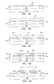
- FIG. 1 illustrates the device structure of a prior art T-RAM cell
- FIG. 2 is a circuit diagram of the prior art T-RAM cell
- FIG. 3 is a top view of a portion of a semiconductor silicon-on-insulator (SOI) wafer having a series of 1F squares for fabricating T-RAM cells according to the present invention
- FIGS. 4A-12 are cross-sectional views illustrating a preferred process for fabricating two adjacent T-RAM cells according to the present invention.
- FIG. 13 is a top view of the two adjacent T-RAM cells fabricated according to the present invention.
- FIG. 14 is a cross-sectional view of the two adjacent T-RAM cells fabricated according to the present invention.
- FIG. 15 is a cross-sectional view of the two adjacent T-RAM cells after formation of a bitline and a bitline contact;
- FIG. 16 is a top view of a portion of a T-RAM array having a plurality of T-RAM cells fabricated according to the present invention.
- FIG. 17 illustrates the device structure of the T-RAM cell according to the present invention.
- the present invention provides a T-RAM array having a plurality of T-RAM cells which are not provided with a vertical thyristor and a surrounding gate as prior art T-RAM cells.
- the T-RAM array of the present invention provides for less control during manufacturing, and is planar and more scalable than prior art T-RAM arrays.
- the present invention also provides a preferred method for fabricating the T-RAM array.
- FIG. 3 is a top view of a portion of a semiconductor silicon-on-insulator (SOI) wafer having a series of 1F squares for fabricating T-RAM cells according to the present invention.
- 1F is a minimum printable dimension by the existing lithographic tool.
- the wafer is designated by reference numeral 100 . It is contemplated that other types of semiconductor wafers besides semiconductor SOI wafers can be used for fabricating T-RAM cells according to the present invention.
- FIGS. 4A-12 there are shown cross-sectional views of the semiconductor wafer 100 for fabricating the two adjacent T-RAM cells.
- the semiconductor wafer 100 is a semiconductor SOI wafer, where active areas for fabricating devices are defined by shallow trench isolations (STI) 110 a, 110 b.
- STI shallow trench isolations
- the semiconductor SOI wafer 100 having a buried oxide layer 136 and silicon layer 20 is used as the substrate to form the T-RAM cells.
- the STIs 110 a , 110 b are formed in a conventional manner.
- a composite sacrificial dielectric layer, e.g., CVD oxide and CVD nitride (e.g., 5 nm and 5 nm, respectively) 30 is deposited.
- a thick insulating layer 40 such as doped glass, or CVD oxide with a thickness of 200 nm is then deposited.
- the insulating layer 40 is patterned to open up gate and channel regions 50 a , 50 b for forming the two adjacent T-RAM cells. Then, p dopant is implanted into the channel regions 50 a , 50 b to provide proper channel threshold adjustment dosage in the channel regions 50 a , 50 b.
- the sacrificial dielectric material in the channel regions 50 a , 50 is then removed, and gate oxides 95 a , 95 b are grown. Then, n+ in-situ doped CVD polysilicon is deposited and planarized back to the insulating layer's surface by the chem-mech polish process. Two polysilicon gate regions 108 a , 108 b are then formed. Photoresist 97 is then patterned to protect the polysilicon gate regions 108 a , 108 b and the exposed insulating layer 40 is removed (see FIG. 4 E).
- a layer of protective dielectric 114 is formed on a top surface of the SOI wafer 100 .
- the thickness of the dielectric layer 114 determines the depth of a gap implant as described below.
- sidewall spacer polysilicon gates 116 a , 116 b are formed along the sidewalls of the deposited polysilicon gate regions 108 a , 108 b .
- the deposited polysilicon gate regions 108 a , 108 b provide the first wordline WL 1 and the sidewall spacer polysilicon gates 116 a , 116 b is the second wordline WL 2 (see FIGS. 15 and 16 ).
- device light drain implant regions 118 a , 118 b with n-type doping implant are formed and then another dielectric layer 112 is formed on top of the sidewall polysilicon spacer gates 116 a , 116 b .
- the implant regions 118 a , 118 b are preferably formed using an n-type arsenic, phosphorus or antimony implant.
- the arsenic implant is at an energy in the range of 50-120 KeV and the quantity used is a dose of between 2E13/cm 2 and 8E13/cm 2 .
- the phosphorus implant is at an energy in the range of 25-60 KeV and the quantity used is a dose of between 2E13/cm 2 and 8E13/cm 2 .
- the antimony implant is at an energy in the range of 25-60 KeV and the quantity used is a dose of between 2E13/cm 2 and 8E13/cm 2 .
- Implant regions 118 a , 118 b are also provided by p-type implants, such as boron and BF2 implants.
- the boron implant is at an energy in the range of 5-30 KeV to a dose of between 4E13/cm 2 and 1E14/cm 2 .
- the BF2 implant is at an energy in the range of 20-120 KeV to a dose of between 4E13/cm 2 and 1E14/cm 2 .
- the structure is annealed using a conventional rapid thermal annealing tool for, preferably, 5 sec/wafer at a temperature range of 900-1025 degrees Celsius.
- a thicker dielectric material 120 is then deposited and chem-mech polished to the polysilicon gate regions 108 a , 108 b (see FIG. 7 ).
- p+ polysilicon Vref wiring regions 122 a , 122 b are formed using a mask and performing reactive ion etching to remove the insulating material 120 to expose lightly doped n-type drain regions below. Then, p+ doped polysilicon is deposited and polished back to the insulating material surface to form the p+ polysilicon Vref wiring regions 122 a , 122 b .
- p+ doped pockets 124 a , 124 b are formed inside of the n-type regions 118 a , 118 b . It is noted that the p+ polysilicon Vref wiring regions 122 a , 122 b are butted to the sidewall spacers 116 a , 116 b to avoid extra n-type doping implants.
- a mask 126 having an opening 128 is used to open up a middle region between the two sidewall spacer polysilicon gates 116 a , 116 b .
- the alignment of the mask 126 is not critical, since a selective etch of oxide to polysilicon is conducted. After etching, only the dielectric material is removed in the region 128 and 133 a , 133 b are created.
- a n+ implant 132 is applied to the structure.
- the opening areas which includes the gaps 133 a , 133 b between sidewall spacer polysilicon gates 116 a , 116 b and the polysilicon gate regions 108 a , 108 b receive the n+ implant 132 to form n+ implant regions 134 a , 134 b , 134 c .
- the gaps are sufficiently wide such that the n+ implant 132 reaches the surface of buried oxide layer 136 .
- n+ implant 132 is an arsenic implant having an energy in the range of 2-15 KeV and the quantity used is a dose of between 8E14/cm 2 and 3E15/cm 2 .
- the structure is again annealed using the conventional rapid thermal annealing tool for, preferably, 5 sec/wafer at a temperature range of 900-1025 degrees Celsius.
- a thin dielectric 138 is deposited and etch-back to the gate surfaces. This dielectric will fill the gaps 133 a , 133 b .
- a common bitline contact region 140 is formed using n+ in-situ doped polysilicon chem-mesh polish to form contact region 140 . This drives the n+ dopant out from contact region 140 to form n++ contact diffusion region 135 .
- FIGS. 13 and 14 illustrate a top view and a cross-sectional view, respectively, of two adjacent T-RAM cells 142 a , 142 b fabricated according to the above described method. These figures show a pair of polysilicon gate regions 108 a , 108 b , a pair of sidewall spacer polysilicon gates 116 a , 116 b , the Vref wiring regions 122 a , 122 b , and the common bitline contact region 140 .
- Each of the T-RAM cells 142 a , 142 b has a size of less than or equal to 6F 2 .
- a bitline 144 and a bitline contact 146 are finally formed over the T-RAM cells 142 a , 142 b.
- FIG. 16 is a top view of a portion of a T-RAM array having a plurality of T-RAM cells 142 fabricated according to the present invention.
- the T-RAM array designated generally by reference numeral 150 has symmetrical right and left T-RAM cells 142 located in a right cell region 152 and a left cell region 154 , respectively.
- Each of the T-RAM cells 142 has a size of less than or equal to 6F 2 .
- Each of the bitlines BL 1 -BL 4 of the portion of the T-RAM array 150 lie in the horizontal direction and pass through a bitline contact 146 located between the right and left T-RAM cells 142 .
- each of the cell regions 152 , 154 also include Vref wiring regions 122 a , 122 b which provide the reference voltage Vref to each of the T-RAM cells 142 . Since the Vref wiring regions 122 a , 122 b are wide, it is contemplated to widen the sidewall spacer wordlines WLR 2 , WLL 2 at the edge of the T-RAM array 150 for better contactability.
- the T-RAM array 150 is designed for incorporation within a memory system.
- FIG. 17 illustrates the device structure of the T-RAM cell 142 according to the present invention.
- the T-RAM cell 142 of the present invention is smaller.
- the T-RAM cell 142 of the present invention is more planar than the prior art T-RAM cell 10 , since it has a lateral-gated, i.e., planar, pnpn thyristor which includes a sidewall spacer switching device.
- the T-RAM cell 142 of the present invention does not have the surrounding gate 14 of the prior art T-RAM cell 10 .
Landscapes
- Semiconductor Memories (AREA)
Abstract
Description
Claims (16)
Priority Applications (1)
| Application Number | Priority Date | Filing Date | Title |
|---|---|---|---|
| US09/760,970 US6552398B2 (en) | 2001-01-16 | 2001-01-16 | T-Ram array having a planar cell structure and method for fabricating the same |
Applications Claiming Priority (1)
| Application Number | Priority Date | Filing Date | Title |
|---|---|---|---|
| US09/760,970 US6552398B2 (en) | 2001-01-16 | 2001-01-16 | T-Ram array having a planar cell structure and method for fabricating the same |
Publications (2)
| Publication Number | Publication Date |
|---|---|
| US20020093030A1 US20020093030A1 (en) | 2002-07-18 |
| US6552398B2 true US6552398B2 (en) | 2003-04-22 |
Family
ID=25060720
Family Applications (1)
| Application Number | Title | Priority Date | Filing Date |
|---|---|---|---|
| US09/760,970 Expired - Fee Related US6552398B2 (en) | 2001-01-16 | 2001-01-16 | T-Ram array having a planar cell structure and method for fabricating the same |
Country Status (1)
| Country | Link |
|---|---|
| US (1) | US6552398B2 (en) |
Cited By (69)
| Publication number | Priority date | Publication date | Assignee | Title |
|---|---|---|---|---|
| US20030032226A1 (en) * | 2001-08-13 | 2003-02-13 | Hitachi, Ltd. | Semiconductor integrated circuit device and method of manufacturing the same |
| US20040124488A1 (en) * | 2001-06-18 | 2004-07-01 | Pierre Fazan | Semiconductor device |
| US20040228168A1 (en) * | 2003-05-13 | 2004-11-18 | Richard Ferrant | Semiconductor memory device and method of operating same |
| US20040227166A1 (en) * | 2003-05-13 | 2004-11-18 | Lionel Portmann | Reference current generator, and method of programming, adjusting and/or operating same |
| US20040238890A1 (en) * | 2002-04-18 | 2004-12-02 | Pierre Fazan | Semiconductor device |
| US20040240306A1 (en) * | 2002-04-18 | 2004-12-02 | Pierre Fazan | Data storage device and refreshing method for use with such device |
| US6845026B1 (en) * | 2003-05-30 | 2005-01-18 | Netlogic Microsystems, Inc. | Thyristor-based content addressable memory (CAM) cells |
| US20050013163A1 (en) * | 2003-05-13 | 2005-01-20 | Richard Ferrant | Semiconductor memory cell, array, architecture and device, and method of operating same |
| US20050017240A1 (en) * | 2003-07-22 | 2005-01-27 | Pierre Fazan | Integrated circuit device, and method of fabricating same |
| US20050063224A1 (en) * | 2003-09-24 | 2005-03-24 | Pierre Fazan | Low power programming technique for a floating body memory transistor, memory cell, and memory array |
| US6888177B1 (en) * | 2002-09-24 | 2005-05-03 | T-Ram, Inc. | Increased base-emitter capacitance |
| US20060091462A1 (en) * | 2004-11-04 | 2006-05-04 | Serguei Okhonin | Memory cell having an electrically floating body transistor and programming technique therefor |
| US20060098481A1 (en) * | 2004-11-10 | 2006-05-11 | Serguei Okhonin | Circuitry for and method of improving statistical distribution of integrated circuits |
| US20060126374A1 (en) * | 2004-12-13 | 2006-06-15 | Waller William K | Sense amplifier circuitry and architecture to write data into and/or read from memory cells |
| US20060131650A1 (en) * | 2004-12-22 | 2006-06-22 | Serguei Okhonin | Bipolar reading technique for a memory cell having an electrically floating body transistor |
| US7078739B1 (en) | 2003-11-12 | 2006-07-18 | T-Ram Semiconductor, Inc. | Thyristor-based memory and its method of operation |
| US20070023833A1 (en) * | 2005-07-28 | 2007-02-01 | Serguei Okhonin | Method for reading a memory cell having an electrically floating body transistor, and memory cell and array implementing same |
| US20070058427A1 (en) * | 2005-09-07 | 2007-03-15 | Serguei Okhonin | Memory cell and memory cell array having an electrically floating body transistor, and methods of operating same |
| US20070064489A1 (en) * | 2005-09-19 | 2007-03-22 | Philippe Bauser | Method and circuitry to generate a reference current for reading a memory cell, and device implementing same |
| US7195959B1 (en) | 2004-10-04 | 2007-03-27 | T-Ram Semiconductor, Inc. | Thyristor-based semiconductor device and method of fabrication |
| US20070085140A1 (en) * | 2005-10-19 | 2007-04-19 | Cedric Bassin | One transistor memory cell having strained electrically floating body region, and method of operating same |
| US20070138530A1 (en) * | 2005-12-19 | 2007-06-21 | Serguei Okhonin | Electrically floating body memory cell and array, and method of operating or controlling same |
| US20070138501A1 (en) * | 2005-12-15 | 2007-06-21 | Sony Corporation | Semiconductor device and method of manufacturing semiconductor device |
| US20070187775A1 (en) * | 2006-02-16 | 2007-08-16 | Serguei Okhonin | Multi-bit memory cell having electrically floating body transistor, and method of programming and reading same |
| US7268373B1 (en) | 2003-11-12 | 2007-09-11 | T-Ram Semiconductor, Inc. | Thyristor-based memory and its method of operation |
| US20070257291A1 (en) * | 2006-05-02 | 2007-11-08 | Serguei Okhonin | Semiconductor memory cell and array using punch-through to program and read same |
| US20070285982A1 (en) * | 2006-04-07 | 2007-12-13 | Eric Carman | Memory array having a programmable word length, and method of operating same |
| US20070297252A1 (en) * | 2006-06-26 | 2007-12-27 | Anant Pratap Singh | Integrated circuit having memory array including ECC and/or column redundancy, and method of programming, controlling and/or operating same |
| US20080013359A1 (en) * | 2006-07-11 | 2008-01-17 | David Fisch | Integrated circuit including memory array having a segmented bit line architecture and method of controlling and/or operating same |
| US20080180995A1 (en) * | 2007-01-26 | 2008-07-31 | Serguei Okhonin | Semiconductor Device With Electrically Floating Body |
| US20080199989A1 (en) * | 2007-02-16 | 2008-08-21 | Sony Corporation | Method of manufacturing semiconductor device |
| US20080237714A1 (en) * | 2007-03-29 | 2008-10-02 | Pierre Fazan | Manufacturing Process for Zero-Capacitor Random Access Memory Circuits |
| US20080298139A1 (en) * | 2007-05-30 | 2008-12-04 | David Fisch | Integrated circuit having voltage generation circuitry for memory cell array, and method of operating and /or controlling same |
| US20090016101A1 (en) * | 2007-06-01 | 2009-01-15 | Serguei Okhonin | Reading Technique for Memory Cell With Electrically Floating Body Transistor |
| US20090146219A1 (en) * | 2007-12-11 | 2009-06-11 | Danngis Liu | Integrated circuit having memory cell array, and method of manufacturing same |
| US7573077B1 (en) * | 2005-05-04 | 2009-08-11 | T-Ram Semiconductor, Inc. | Thyristor-based semiconductor memory device with back-gate bias |
| US20090200612A1 (en) * | 2008-02-08 | 2009-08-13 | Viktor Koldiaev | Integrated Circuit Having Memory Cells Including Gate Material Having High Work Function, and Method of Manufacturing Same |
| US20090201723A1 (en) * | 2008-02-06 | 2009-08-13 | Serguei Okhonin | Single Transistor Memory Cell |
| US7592642B1 (en) | 2003-09-25 | 2009-09-22 | T-Ram Semiconductor, Inc. | Thyristor-based semiconductor device with indium-carbon implant and method of fabrication |
| US20090251958A1 (en) * | 2008-04-04 | 2009-10-08 | Philippe Bauser | Read circuitry for an integrated circuit having memory cells and/or a memory cell array, and method of operating same |
| US7606098B2 (en) | 2006-04-18 | 2009-10-20 | Innovative Silicon Isi Sa | Semiconductor memory array architecture with grouped memory cells, and method of controlling same |
| US20100075471A1 (en) * | 2008-09-25 | 2010-03-25 | Innovative Silicon Isi Sa | Recessed Gate Silicon-On-Insulator Floating Body Device With Self-Aligned Lateral Isolation |
| US20100091586A1 (en) * | 2008-10-15 | 2010-04-15 | Innovative Silicon Isi Sa | Techniques for simultaneously driving a plurality of source lines |
| US20100110816A1 (en) * | 2008-11-05 | 2010-05-06 | Innovative Silicon Isi Sa | Techniques for block refreshing a semiconductor memory device |
| US20100142294A1 (en) * | 2008-12-05 | 2010-06-10 | Eric Carman | Vertical Transistor Memory Cell and Array |
| US20100210075A1 (en) * | 2009-02-18 | 2010-08-19 | Innovative Silicon Isi Sa | Techniques for providing a source line plane |
| US20100259964A1 (en) * | 2009-03-31 | 2010-10-14 | Innovative Silicon Isi Sa | Techniques for providing a semiconductor memory device |
| US20100271858A1 (en) * | 2009-04-27 | 2010-10-28 | Innovative Silicon Isi Sa | Techniques for providing a direct injection semiconductor memory device having ganged carrier injection lines |
| US20100277982A1 (en) * | 2009-04-30 | 2010-11-04 | Innovative Silicon Isi Sa | Semiconductor device with floating gate and electrically floating body |
| US20100296327A1 (en) * | 2009-05-22 | 2010-11-25 | Innovative Silicon Isi Sa | Techniques for providing a direct injection semiconductor memory device |
| US20110007578A1 (en) * | 2009-07-10 | 2011-01-13 | Innovative Silicon Isi Sa | Techniques for providing a semiconductor memory device |
| US20110019482A1 (en) * | 2009-07-27 | 2011-01-27 | Innovative Silicon Isi Sa | Techniques for providing a direct injection semiconductor memory device |
| US20110058436A1 (en) * | 2009-09-04 | 2011-03-10 | Innovative Silicon Isi Sa | Techniques for sensing a semiconductor memory device |
| US7933140B2 (en) | 2008-10-02 | 2011-04-26 | Micron Technology, Inc. | Techniques for reducing a voltage swing |
| US20110122687A1 (en) * | 2009-11-24 | 2011-05-26 | Innovative Silicon Isi Sa | Techniques for reducing disturbance in a semiconductor device |
| US20110141836A1 (en) * | 2009-12-16 | 2011-06-16 | Innovative Silicon Isi Sa | Techniques for reducing impact of array disturbs in a semiconductor memory device |
| US20110199848A1 (en) * | 2010-02-12 | 2011-08-18 | Innovative Silicon Isi Sa | Techniques for controlling a semiconductor memory device |
| US20110216605A1 (en) * | 2010-03-04 | 2011-09-08 | Innovative Silicon Isi Sa | Techniques for providing a semiconductor memory device having hierarchical bit lines |
| US20110216617A1 (en) * | 2010-03-04 | 2011-09-08 | Innovative Silicon Isi Sa | Techniques for sensing a semiconductor memory device |
| US20110216608A1 (en) * | 2010-03-05 | 2011-09-08 | Innovative Silicon Isi Sa | Techniques for reading from and/or writing to a semiconductor memory device |
| US8174046B1 (en) * | 2006-02-23 | 2012-05-08 | T-Ram Semiconductor, Inc | Reducing effects of parasitic transistors in thyristor-based memory using local thinning or implanting |
| US8194487B2 (en) | 2007-09-17 | 2012-06-05 | Micron Technology, Inc. | Refreshing data of memory cells with electrically floating body transistors |
| US8411524B2 (en) | 2010-05-06 | 2013-04-02 | Micron Technology, Inc. | Techniques for refreshing a semiconductor memory device |
| US8531878B2 (en) | 2011-05-17 | 2013-09-10 | Micron Technology, Inc. | Techniques for providing a semiconductor memory device |
| US8536628B2 (en) | 2007-11-29 | 2013-09-17 | Micron Technology, Inc. | Integrated circuit having memory cell array including barriers, and method of manufacturing same |
| US8547738B2 (en) | 2010-03-15 | 2013-10-01 | Micron Technology, Inc. | Techniques for providing a semiconductor memory device |
| US8710566B2 (en) | 2009-03-04 | 2014-04-29 | Micron Technology, Inc. | Techniques for forming a contact to a buried diffusion layer in a semiconductor memory device |
| US8773933B2 (en) | 2012-03-16 | 2014-07-08 | Micron Technology, Inc. | Techniques for accessing memory cells |
| US9559216B2 (en) | 2011-06-06 | 2017-01-31 | Micron Technology, Inc. | Semiconductor memory device and method for biasing same |
Families Citing this family (33)
| Publication number | Priority date | Publication date | Assignee | Title |
|---|---|---|---|---|
| US6690038B1 (en) | 1999-06-05 | 2004-02-10 | T-Ram, Inc. | Thyristor-based device over substrate surface |
| US6559470B2 (en) | 2000-06-22 | 2003-05-06 | Progressed Technologies, Inc. | Negative differential resistance field effect transistor (NDR-FET) and circuits using the same |
| US6594193B2 (en) | 2000-06-22 | 2003-07-15 | Progressent Technologies, Inc. | Charge pump for negative differential resistance transistor |
| US6724655B2 (en) * | 2000-06-22 | 2004-04-20 | Progressant Technologies, Inc. | Memory cell using negative differential resistance field effect transistors |
| US6727528B1 (en) | 2001-03-22 | 2004-04-27 | T-Ram, Inc. | Thyristor-based device including trench dielectric isolation for thyristor-body regions |
| US7456439B1 (en) | 2001-03-22 | 2008-11-25 | T-Ram Semiconductor, Inc. | Vertical thyristor-based memory with trench isolation and its method of fabrication |
| US6583452B1 (en) * | 2001-12-17 | 2003-06-24 | T-Ram, Inc. | Thyristor-based device having extended capacitive coupling |
| US7453083B2 (en) * | 2001-12-21 | 2008-11-18 | Synopsys, Inc. | Negative differential resistance field effect transistor for implementing a pull up element in a memory cell |
| US6956262B1 (en) | 2001-12-21 | 2005-10-18 | Synopsys Inc. | Charge trapping pull up element |
| US6861707B1 (en) * | 2002-06-28 | 2005-03-01 | Progressant Technologies, Inc. | Negative differential resistance (NDR) memory cell with reduced soft error rate |
| US7098472B2 (en) * | 2002-06-28 | 2006-08-29 | Progressant Technologies, Inc. | Negative differential resistance (NDR) elements and memory device using the same |
| US6795337B2 (en) | 2002-06-28 | 2004-09-21 | Progressant Technologies, Inc. | Negative differential resistance (NDR) elements and memory device using the same |
| US6847562B2 (en) * | 2002-06-28 | 2005-01-25 | Progressant Technologies, Inc. | Enhanced read and write methods for negative differential resistance (NDR) based memory device |
| US6567292B1 (en) | 2002-06-28 | 2003-05-20 | Progressant Technologies, Inc. | Negative differential resistance (NDR) element and memory with reduced soft error rate |
| US7095659B2 (en) * | 2002-06-28 | 2006-08-22 | Progressant Technologies, Inc. | Variable voltage supply bias and methods for negative differential resistance (NDR) based memory device |
| US6912151B2 (en) * | 2002-06-28 | 2005-06-28 | Synopsys, Inc. | Negative differential resistance (NDR) based memory device with reduced body effects |
| US6864104B2 (en) * | 2002-06-28 | 2005-03-08 | Progressant Technologies, Inc. | Silicon on insulator (SOI) negative differential resistance (NDR) based memory device with reduced body effects |
| US7125753B1 (en) | 2002-10-01 | 2006-10-24 | T-Ram Semiconductor, Inc. | Self-aligned thin capacitively-coupled thyristor structure |
| US6767770B1 (en) | 2002-10-01 | 2004-07-27 | T-Ram, Inc. | Method of forming self-aligned thin capacitively-coupled thyristor structure |
| US6965129B1 (en) | 2002-11-06 | 2005-11-15 | T-Ram, Inc. | Thyristor-based device having dual control ports |
| US6980467B2 (en) * | 2002-12-09 | 2005-12-27 | Progressant Technologies, Inc. | Method of forming a negative differential resistance device |
| US6812084B2 (en) * | 2002-12-09 | 2004-11-02 | Progressant Technologies, Inc. | Adaptive negative differential resistance device |
| US6806117B2 (en) * | 2002-12-09 | 2004-10-19 | Progressant Technologies, Inc. | Methods of testing/stressing a charge trapping device |
| US6849483B2 (en) * | 2002-12-09 | 2005-02-01 | Progressant Technologies, Inc. | Charge trapping device and method of forming the same |
| US6979580B2 (en) * | 2002-12-09 | 2005-12-27 | Progressant Technologies, Inc. | Process for controlling performance characteristics of a negative differential resistance (NDR) device |
| US7012833B2 (en) * | 2002-12-09 | 2006-03-14 | Progressant Technologies, Inc. | Integrated circuit having negative differential resistance (NDR) devices with varied peak-to-valley ratios (PVRs) |
| US7005711B2 (en) * | 2002-12-20 | 2006-02-28 | Progressant Technologies, Inc. | N-channel pull-up element and logic circuit |
| US6849481B1 (en) * | 2003-07-28 | 2005-02-01 | Chartered Semiconductor Manufacturing Ltd. | Thyristor-based SRAM and method for the fabrication thereof |
| TWI240439B (en) * | 2003-09-24 | 2005-09-21 | Sanken Electric Co Ltd | Nitride semiconductor device and manufacturing method thereof |
| TWI243399B (en) * | 2003-09-24 | 2005-11-11 | Sanken Electric Co Ltd | Nitride semiconductor device |
| US7368775B2 (en) * | 2004-07-31 | 2008-05-06 | Taiwan Semiconductor Manufacturing Co., Ltd. | Single transistor DRAM cell with reduced current leakage and method of manufacture |
| US20070257326A1 (en) * | 2006-05-08 | 2007-11-08 | Chien-Li Kuo | Integrated circuit structure and method of manufacturing a memory cell |
| US8535992B2 (en) | 2010-06-29 | 2013-09-17 | Micron Technology, Inc. | Thyristor random access memory device and method |
Citations (2)
| Publication number | Priority date | Publication date | Assignee | Title |
|---|---|---|---|---|
| US5824584A (en) * | 1997-06-16 | 1998-10-20 | Motorola, Inc. | Method of making and accessing split gate memory device |
| US6104045A (en) * | 1998-05-13 | 2000-08-15 | Micron Technology, Inc. | High density planar SRAM cell using bipolar latch-up and gated diode breakdown |
-
2001
- 2001-01-16 US US09/760,970 patent/US6552398B2/en not_active Expired - Fee Related
Patent Citations (2)
| Publication number | Priority date | Publication date | Assignee | Title |
|---|---|---|---|---|
| US5824584A (en) * | 1997-06-16 | 1998-10-20 | Motorola, Inc. | Method of making and accessing split gate memory device |
| US6104045A (en) * | 1998-05-13 | 2000-08-15 | Micron Technology, Inc. | High density planar SRAM cell using bipolar latch-up and gated diode breakdown |
Non-Patent Citations (2)
| Title |
|---|
| A Novel High Density, Low Voltage SRAM Cell with a Vertical NDR Device, by Farid Nemati and James D. Plummer, Center for Integrated Systems, Stanford University, 1998. |
| A Novel-Thyristor-based SRAM cell(T-RAM) for High-Speed, Low-Voltage, Giga-scale Memories by Farid Nemati and James D. Plummer, Center for Integrated Systems, Stanford, University, 1999. |
Cited By (218)
| Publication number | Priority date | Publication date | Assignee | Title |
|---|---|---|---|---|
| US6873539B1 (en) | 2001-06-18 | 2005-03-29 | Pierre Fazan | Semiconductor device |
| US20080068882A1 (en) * | 2001-06-18 | 2008-03-20 | Pierre Fazan | Semiconductor device |
| US7280399B2 (en) | 2001-06-18 | 2007-10-09 | Innovative Silicon S.A. | Semiconductor device |
| US20040124488A1 (en) * | 2001-06-18 | 2004-07-01 | Pierre Fazan | Semiconductor device |
| US20040135202A1 (en) * | 2001-06-18 | 2004-07-15 | Pierre Fazan | Semiconductor device |
| US20040159876A1 (en) * | 2001-06-18 | 2004-08-19 | Pierre Fazan | Semiconductor device |
| US20080055974A1 (en) * | 2001-06-18 | 2008-03-06 | Pierre Fazan | Semiconductor device |
| US7239549B2 (en) | 2001-06-18 | 2007-07-03 | Innovative Silicon S.A. | Semiconductor device |
| US7732816B2 (en) | 2001-06-18 | 2010-06-08 | Innovative Silicon Isi Sa | Semiconductor device |
| US20050280028A1 (en) * | 2001-06-18 | 2005-12-22 | Pierre Fazan | Semiconductor device |
| US6969662B2 (en) | 2001-06-18 | 2005-11-29 | Pierre Fazan | Semiconductor device |
| US6934186B2 (en) | 2001-06-18 | 2005-08-23 | Innovative Silicon S.A. | Semiconductor device |
| US20050213379A1 (en) * | 2001-06-18 | 2005-09-29 | Pierre Fazan | Semiconductor device |
| US6937516B2 (en) | 2001-06-18 | 2005-08-30 | Innovative Silicon S.A. | Semiconductor device |
| US7541616B2 (en) | 2001-06-18 | 2009-06-02 | Innovative Silicon Isi Sa | Semiconductor device |
| US6925006B2 (en) | 2001-06-18 | 2005-08-02 | Innovative Silicon S.A. | Semiconductor device |
| US6930918B2 (en) | 2001-06-18 | 2005-08-16 | Innovative Silicon S.A. | Semiconductor device |
| US20030132465A1 (en) * | 2001-08-13 | 2003-07-17 | Hitachi, Ltd. | Semiconductor integrated circuit device and method of manufacturing the same |
| US6933564B2 (en) | 2001-08-13 | 2005-08-23 | Renesas Technology Corp. | Semiconductor integrated circuit device and method of manufacturing the same |
| US20030032226A1 (en) * | 2001-08-13 | 2003-02-13 | Hitachi, Ltd. | Semiconductor integrated circuit device and method of manufacturing the same |
| US6706582B2 (en) * | 2001-08-13 | 2004-03-16 | Renesas Technology Corporation | Semiconductor integrated circuit device and method of manufacturing the same |
| US20040238890A1 (en) * | 2002-04-18 | 2004-12-02 | Pierre Fazan | Semiconductor device |
| US20050128851A1 (en) * | 2002-04-18 | 2005-06-16 | Pierre Fazan | Data storage device and refreshing method for use with such device |
| US7061050B2 (en) | 2002-04-18 | 2006-06-13 | Innovative Silicon S.A. | Semiconductor device utilizing both fully and partially depleted devices |
| US7170807B2 (en) | 2002-04-18 | 2007-01-30 | Innovative Silicon S.A. | Data storage device and refreshing method for use with such device |
| US7514748B2 (en) | 2002-04-18 | 2009-04-07 | Innovative Silicon Isi Sa | Semiconductor device |
| US20070109896A1 (en) * | 2002-04-18 | 2007-05-17 | Pierre Fazan | Data storage device and refreshing method for use with such device |
| US7342842B2 (en) | 2002-04-18 | 2008-03-11 | Innovative Silicon, S.A. | Data storage device and refreshing method for use with such device |
| US20040240306A1 (en) * | 2002-04-18 | 2004-12-02 | Pierre Fazan | Data storage device and refreshing method for use with such device |
| US6982918B2 (en) | 2002-04-18 | 2006-01-03 | Pierre Fazan | Data storage device and refreshing method for use with such device |
| US6888177B1 (en) * | 2002-09-24 | 2005-05-03 | T-Ram, Inc. | Increased base-emitter capacitance |
| US6912150B2 (en) | 2003-05-13 | 2005-06-28 | Lionel Portman | Reference current generator, and method of programming, adjusting and/or operating same |
| US7187581B2 (en) | 2003-05-13 | 2007-03-06 | Innovative Silicon S.A. | Semiconductor memory device and method of operating same |
| US20050013163A1 (en) * | 2003-05-13 | 2005-01-20 | Richard Ferrant | Semiconductor memory cell, array, architecture and device, and method of operating same |
| US20050174873A1 (en) * | 2003-05-13 | 2005-08-11 | Richard Ferrant | Semiconductor memory device and method of operating same |
| US7733693B2 (en) | 2003-05-13 | 2010-06-08 | Innovative Silicon Isi Sa | Semiconductor memory device and method of operating same |
| US20050162931A1 (en) * | 2003-05-13 | 2005-07-28 | Lionel Portmann | Reference current generator, and method of programming, adjusting and/or operating same |
| US20040228168A1 (en) * | 2003-05-13 | 2004-11-18 | Richard Ferrant | Semiconductor memory device and method of operating same |
| US7085153B2 (en) | 2003-05-13 | 2006-08-01 | Innovative Silicon S.A. | Semiconductor memory cell, array, architecture and device, and method of operating same |
| US20050157580A1 (en) * | 2003-05-13 | 2005-07-21 | Richard Ferrant | Semiconductor memory device and method of operating same |
| US7359229B2 (en) | 2003-05-13 | 2008-04-15 | Innovative Silicon S.A. | Semiconductor memory device and method of operating same |
| US6980461B2 (en) | 2003-05-13 | 2005-12-27 | Innovative Silicon S.A. | Reference current generator, and method of programming, adjusting and/or operating same |
| US20070159911A1 (en) * | 2003-05-13 | 2007-07-12 | Richard Ferrant | Semiconductor memory device and method of operating same |
| US20080205114A1 (en) * | 2003-05-13 | 2008-08-28 | Richard Ferrant | Semiconductor memory device and method of operating same |
| US7085156B2 (en) | 2003-05-13 | 2006-08-01 | Innovative Silicon S.A. | Semiconductor memory device and method of operating same |
| US20040227166A1 (en) * | 2003-05-13 | 2004-11-18 | Lionel Portmann | Reference current generator, and method of programming, adjusting and/or operating same |
| US6845026B1 (en) * | 2003-05-30 | 2005-01-18 | Netlogic Microsystems, Inc. | Thyristor-based content addressable memory (CAM) cells |
| US20080153213A1 (en) * | 2003-07-22 | 2008-06-26 | Pierre Fazan | Integrated circuit device, and method of fabricating same |
| US7736959B2 (en) | 2003-07-22 | 2010-06-15 | Innovative Silicon Isi Sa | Integrated circuit device, and method of fabricating same |
| US20050017240A1 (en) * | 2003-07-22 | 2005-01-27 | Pierre Fazan | Integrated circuit device, and method of fabricating same |
| US7335934B2 (en) | 2003-07-22 | 2008-02-26 | Innovative Silicon S.A. | Integrated circuit device, and method of fabricating same |
| US7184298B2 (en) | 2003-09-24 | 2007-02-27 | Innovative Silicon S.A. | Low power programming technique for a floating body memory transistor, memory cell, and memory array |
| US20050063224A1 (en) * | 2003-09-24 | 2005-03-24 | Pierre Fazan | Low power programming technique for a floating body memory transistor, memory cell, and memory array |
| US7177175B2 (en) | 2003-09-24 | 2007-02-13 | Innovative Silicon S.A. | Low power programming technique for a floating body memory transistor, memory cell, and memory array |
| US20060114717A1 (en) * | 2003-09-24 | 2006-06-01 | Pierre Fazan | Low power programming technique for a floating body memory transistor, memory cell, and memory array |
| US7592642B1 (en) | 2003-09-25 | 2009-09-22 | T-Ram Semiconductor, Inc. | Thyristor-based semiconductor device with indium-carbon implant and method of fabrication |
| US7268373B1 (en) | 2003-11-12 | 2007-09-11 | T-Ram Semiconductor, Inc. | Thyristor-based memory and its method of operation |
| US7893456B1 (en) | 2003-11-12 | 2011-02-22 | T-Ram Semiconductor, Inc. | Thyristor-based memory and its method of operation |
| US7488627B1 (en) | 2003-11-12 | 2009-02-10 | T-Ram Semiconductor, Inc. | Thyristor-based memory and its method of operation |
| US7078739B1 (en) | 2003-11-12 | 2006-07-18 | T-Ram Semiconductor, Inc. | Thyristor-based memory and its method of operation |
| US7195959B1 (en) | 2004-10-04 | 2007-03-27 | T-Ram Semiconductor, Inc. | Thyristor-based semiconductor device and method of fabrication |
| US20060091462A1 (en) * | 2004-11-04 | 2006-05-04 | Serguei Okhonin | Memory cell having an electrically floating body transistor and programming technique therefor |
| US7476939B2 (en) | 2004-11-04 | 2009-01-13 | Innovative Silicon Isi Sa | Memory cell having an electrically floating body transistor and programming technique therefor |
| US20060098481A1 (en) * | 2004-11-10 | 2006-05-11 | Serguei Okhonin | Circuitry for and method of improving statistical distribution of integrated circuits |
| US7251164B2 (en) | 2004-11-10 | 2007-07-31 | Innovative Silicon S.A. | Circuitry for and method of improving statistical distribution of integrated circuits |
| US20060126374A1 (en) * | 2004-12-13 | 2006-06-15 | Waller William K | Sense amplifier circuitry and architecture to write data into and/or read from memory cells |
| US7301838B2 (en) | 2004-12-13 | 2007-11-27 | Innovative Silicon S.A. | Sense amplifier circuitry and architecture to write data into and/or read from memory cells |
| US7486563B2 (en) | 2004-12-13 | 2009-02-03 | Innovative Silicon Isi Sa | Sense amplifier circuitry and architecture to write data into and/or read from memory cells |
| US20080025083A1 (en) * | 2004-12-22 | 2008-01-31 | Serguei Okhonin | Bipolar reading technique for a memory cell having an electrically floating body transistor |
| US7477540B2 (en) | 2004-12-22 | 2009-01-13 | Innovative Silicon Isi Sa | Bipolar reading technique for a memory cell having an electrically floating body transistor |
| US7301803B2 (en) | 2004-12-22 | 2007-11-27 | Innovative Silicon S.A. | Bipolar reading technique for a memory cell having an electrically floating body transistor |
| US20060131650A1 (en) * | 2004-12-22 | 2006-06-22 | Serguei Okhonin | Bipolar reading technique for a memory cell having an electrically floating body transistor |
| US7573077B1 (en) * | 2005-05-04 | 2009-08-11 | T-Ram Semiconductor, Inc. | Thyristor-based semiconductor memory device with back-gate bias |
| US20070023833A1 (en) * | 2005-07-28 | 2007-02-01 | Serguei Okhonin | Method for reading a memory cell having an electrically floating body transistor, and memory cell and array implementing same |
| US20100020597A1 (en) * | 2005-09-07 | 2010-01-28 | Serguei Okhonin | Memory Cell and Memory Cell Array Having an Electrically Floating Body Transistor, and Methods of Operating Same |
| US7606066B2 (en) | 2005-09-07 | 2009-10-20 | Innovative Silicon Isi Sa | Memory cell and memory cell array having an electrically floating body transistor, and methods of operating same |
| US8873283B2 (en) | 2005-09-07 | 2014-10-28 | Micron Technology, Inc. | Memory cell and memory cell array having an electrically floating body transistor, and methods of operating same |
| US11031069B2 (en) | 2005-09-07 | 2021-06-08 | Ovonyx Memory Technology, Llc | Memory cell and memory cell array having an electrically floating body transistor, and methods of operating same |
| US10418091B2 (en) | 2005-09-07 | 2019-09-17 | Ovonyx Memory Technology, Llc | Memory cell and memory cell array having an electrically floating body transistor, and methods of operating same |
| US20070058427A1 (en) * | 2005-09-07 | 2007-03-15 | Serguei Okhonin | Memory cell and memory cell array having an electrically floating body transistor, and methods of operating same |
| US20070064489A1 (en) * | 2005-09-19 | 2007-03-22 | Philippe Bauser | Method and circuitry to generate a reference current for reading a memory cell, and device implementing same |
| US7355916B2 (en) | 2005-09-19 | 2008-04-08 | Innovative Silicon S.A. | Method and circuitry to generate a reference current for reading a memory cell, and device implementing same |
| US7499358B2 (en) | 2005-09-19 | 2009-03-03 | Innovative Silicon Isi Sa | Method and circuitry to generate a reference current for reading a memory cell, and device implementing same |
| US20070085140A1 (en) * | 2005-10-19 | 2007-04-19 | Cedric Bassin | One transistor memory cell having strained electrically floating body region, and method of operating same |
| US20070138501A1 (en) * | 2005-12-15 | 2007-06-21 | Sony Corporation | Semiconductor device and method of manufacturing semiconductor device |
| US7683430B2 (en) | 2005-12-19 | 2010-03-23 | Innovative Silicon Isi Sa | Electrically floating body memory cell and array, and method of operating or controlling same |
| US20070138530A1 (en) * | 2005-12-19 | 2007-06-21 | Serguei Okhonin | Electrically floating body memory cell and array, and method of operating or controlling same |
| US20070187775A1 (en) * | 2006-02-16 | 2007-08-16 | Serguei Okhonin | Multi-bit memory cell having electrically floating body transistor, and method of programming and reading same |
| US7542345B2 (en) | 2006-02-16 | 2009-06-02 | Innovative Silicon Isi Sa | Multi-bit memory cell having electrically floating body transistor, and method of programming and reading same |
| US8174046B1 (en) * | 2006-02-23 | 2012-05-08 | T-Ram Semiconductor, Inc | Reducing effects of parasitic transistors in thyristor-based memory using local thinning or implanting |
| US8134867B2 (en) | 2006-04-07 | 2012-03-13 | Micron Technology, Inc. | Memory array having a programmable word length, and method of operating same |
| US20090141550A1 (en) * | 2006-04-07 | 2009-06-04 | Eric Carman | Memory Array Having a Programmable Word Length, and Method of Operating Same |
| US20070285982A1 (en) * | 2006-04-07 | 2007-12-13 | Eric Carman | Memory array having a programmable word length, and method of operating same |
| US7492632B2 (en) | 2006-04-07 | 2009-02-17 | Innovative Silicon Isi Sa | Memory array having a programmable word length, and method of operating same |
| US7940559B2 (en) | 2006-04-07 | 2011-05-10 | Micron Technology, Inc. | Memory array having a programmable word length, and method of operating same |
| US7606098B2 (en) | 2006-04-18 | 2009-10-20 | Innovative Silicon Isi Sa | Semiconductor memory array architecture with grouped memory cells, and method of controlling same |
| US20110194363A1 (en) * | 2006-05-02 | 2011-08-11 | Micron Technology, Inc. | Semiconductor memory cell and array using punch-through to program and read same |
| US20070257291A1 (en) * | 2006-05-02 | 2007-11-08 | Serguei Okhonin | Semiconductor memory cell and array using punch-through to program and read same |
| US7933142B2 (en) | 2006-05-02 | 2011-04-26 | Micron Technology, Inc. | Semiconductor memory cell and array using punch-through to program and read same |
| US8295078B2 (en) | 2006-05-02 | 2012-10-23 | Micron Technology, Inc. | Semiconductor memory cell and array using punch-through to program and read same |
| US8069377B2 (en) | 2006-06-26 | 2011-11-29 | Micron Technology, Inc. | Integrated circuit having memory array including ECC and column redundancy and method of operating the same |
| US20070297252A1 (en) * | 2006-06-26 | 2007-12-27 | Anant Pratap Singh | Integrated circuit having memory array including ECC and/or column redundancy, and method of programming, controlling and/or operating same |
| US8402326B2 (en) | 2006-06-26 | 2013-03-19 | Micron Technology, Inc. | Integrated circuit having memory array including ECC and column redundancy and method of operating same |
| US7542340B2 (en) | 2006-07-11 | 2009-06-02 | Innovative Silicon Isi Sa | Integrated circuit including memory array having a segmented bit line architecture and method of controlling and/or operating same |
| US20080013359A1 (en) * | 2006-07-11 | 2008-01-17 | David Fisch | Integrated circuit including memory array having a segmented bit line architecture and method of controlling and/or operating same |
| US8395937B2 (en) | 2006-07-11 | 2013-03-12 | Micron Technology, Inc. | Integrated circuit including memory array having a segmented bit line architecture and method of controlling and/or operating same |
| US7969779B2 (en) | 2006-07-11 | 2011-06-28 | Micron Technology, Inc. | Integrated circuit including memory array having a segmented bit line architecture and method of controlling and/or operating same |
| US20090231898A1 (en) * | 2006-07-11 | 2009-09-17 | David Fisch | Integrated Circuit Including Memory Array Having a Segmented Bit Line Architecture and Method of Controlling and/or Operating Same |
| US20080180995A1 (en) * | 2007-01-26 | 2008-07-31 | Serguei Okhonin | Semiconductor Device With Electrically Floating Body |
| US8264041B2 (en) | 2007-01-26 | 2012-09-11 | Micron Technology, Inc. | Semiconductor device with electrically floating body |
| US8492209B2 (en) | 2007-01-26 | 2013-07-23 | Micron Technology, Inc. | Semiconductor device with electrically floating body |
| US8796770B2 (en) | 2007-01-26 | 2014-08-05 | Micron Technology, Inc. | Semiconductor device with electrically floating body |
| US7531389B2 (en) * | 2007-02-16 | 2009-05-12 | Sony Corporation | Method of manufacturing semiconductor device |
| US20080199989A1 (en) * | 2007-02-16 | 2008-08-21 | Sony Corporation | Method of manufacturing semiconductor device |
| US20080237714A1 (en) * | 2007-03-29 | 2008-10-02 | Pierre Fazan | Manufacturing Process for Zero-Capacitor Random Access Memory Circuits |
| US9276000B2 (en) | 2007-03-29 | 2016-03-01 | Micron Technology, Inc. | Manufacturing process for zero-capacitor random access memory circuits |
| US8518774B2 (en) | 2007-03-29 | 2013-08-27 | Micron Technology, Inc. | Manufacturing process for zero-capacitor random access memory circuits |
| US9257155B2 (en) | 2007-05-30 | 2016-02-09 | Micron Technology, Inc. | Integrated circuit having voltage generation circuitry for memory cell array, and method of operating and/or controlling same |
| US8064274B2 (en) | 2007-05-30 | 2011-11-22 | Micron Technology, Inc. | Integrated circuit having voltage generation circuitry for memory cell array, and method of operating and/or controlling same |
| US8659956B2 (en) | 2007-05-30 | 2014-02-25 | Micron Technology, Inc. | Integrated circuit having voltage generation circuitry for memory cell array, and method of operating and/or controlling same |
| US20080298139A1 (en) * | 2007-05-30 | 2008-12-04 | David Fisch | Integrated circuit having voltage generation circuitry for memory cell array, and method of operating and /or controlling same |
| US8085594B2 (en) | 2007-06-01 | 2011-12-27 | Micron Technology, Inc. | Reading technique for memory cell with electrically floating body transistor |
| US20090016101A1 (en) * | 2007-06-01 | 2009-01-15 | Serguei Okhonin | Reading Technique for Memory Cell With Electrically Floating Body Transistor |
| US8659948B2 (en) | 2007-06-01 | 2014-02-25 | Micron Technology, Inc. | Techniques for reading a memory cell with electrically floating body transistor |
| US8797819B2 (en) | 2007-09-17 | 2014-08-05 | Micron Technology, Inc. | Refreshing data of memory cells with electrically floating body transistors |
| US8446794B2 (en) | 2007-09-17 | 2013-05-21 | Micron Technology, Inc. | Refreshing data of memory cells with electrically floating body transistors |
| US8194487B2 (en) | 2007-09-17 | 2012-06-05 | Micron Technology, Inc. | Refreshing data of memory cells with electrically floating body transistors |
| US10304837B2 (en) | 2007-11-29 | 2019-05-28 | Ovonyx Memory Technology, Llc | Integrated circuit having memory cell array including barriers, and method of manufacturing same |
| US11081486B2 (en) | 2007-11-29 | 2021-08-03 | Ovonyx Memory Technology, Llc | Integrated circuit having memory cell array including barriers, and method of manufacturing same |
| US8536628B2 (en) | 2007-11-29 | 2013-09-17 | Micron Technology, Inc. | Integrated circuit having memory cell array including barriers, and method of manufacturing same |
| US20090146219A1 (en) * | 2007-12-11 | 2009-06-11 | Danngis Liu | Integrated circuit having memory cell array, and method of manufacturing same |
| US8349662B2 (en) | 2007-12-11 | 2013-01-08 | Micron Technology, Inc. | Integrated circuit having memory cell array, and method of manufacturing same |
| US9019788B2 (en) | 2008-01-24 | 2015-04-28 | Micron Technology, Inc. | Techniques for accessing memory cells |
| US20090201723A1 (en) * | 2008-02-06 | 2009-08-13 | Serguei Okhonin | Single Transistor Memory Cell |
| US8014195B2 (en) | 2008-02-06 | 2011-09-06 | Micron Technology, Inc. | Single transistor memory cell |
| US8325515B2 (en) | 2008-02-06 | 2012-12-04 | Micron Technology, Inc. | Integrated circuit device |
| US20090200612A1 (en) * | 2008-02-08 | 2009-08-13 | Viktor Koldiaev | Integrated Circuit Having Memory Cells Including Gate Material Having High Work Function, and Method of Manufacturing Same |
| US8189376B2 (en) | 2008-02-08 | 2012-05-29 | Micron Technology, Inc. | Integrated circuit having memory cells including gate material having high work function, and method of manufacturing same |
| US20090251958A1 (en) * | 2008-04-04 | 2009-10-08 | Philippe Bauser | Read circuitry for an integrated circuit having memory cells and/or a memory cell array, and method of operating same |
| US8274849B2 (en) | 2008-04-04 | 2012-09-25 | Micron Technology, Inc. | Read circuitry for an integrated circuit having memory cells and/or a memory cell array, and method of operating same |
| US7957206B2 (en) | 2008-04-04 | 2011-06-07 | Micron Technology, Inc. | Read circuitry for an integrated circuit having memory cells and/or a memory cell array, and method of operating same |
| US20110223726A1 (en) * | 2008-09-25 | 2011-09-15 | Micron Technology, Inc. | Recessed gate silicon-on-insulator floating body device with self-aligned lateral isolation |
| US20100075471A1 (en) * | 2008-09-25 | 2010-03-25 | Innovative Silicon Isi Sa | Recessed Gate Silicon-On-Insulator Floating Body Device With Self-Aligned Lateral Isolation |
| US9553186B2 (en) | 2008-09-25 | 2017-01-24 | Micron Technology, Inc. | Recessed gate silicon-on-insulator floating body device with self-aligned lateral isolation |
| US8790968B2 (en) | 2008-09-25 | 2014-07-29 | Micron Technology, Inc. | Recessed gate silicon-on-insulator floating body device with self-aligned lateral isolation |
| US7947543B2 (en) | 2008-09-25 | 2011-05-24 | Micron Technology, Inc. | Recessed gate silicon-on-insulator floating body device with self-aligned lateral isolation |
| US7933140B2 (en) | 2008-10-02 | 2011-04-26 | Micron Technology, Inc. | Techniques for reducing a voltage swing |
| US8315083B2 (en) | 2008-10-02 | 2012-11-20 | Micron Technology Inc. | Techniques for reducing a voltage swing |
| US7924630B2 (en) | 2008-10-15 | 2011-04-12 | Micron Technology, Inc. | Techniques for simultaneously driving a plurality of source lines |
| US20100091586A1 (en) * | 2008-10-15 | 2010-04-15 | Innovative Silicon Isi Sa | Techniques for simultaneously driving a plurality of source lines |
| US8223574B2 (en) | 2008-11-05 | 2012-07-17 | Micron Technology, Inc. | Techniques for block refreshing a semiconductor memory device |
| US20100110816A1 (en) * | 2008-11-05 | 2010-05-06 | Innovative Silicon Isi Sa | Techniques for block refreshing a semiconductor memory device |
| US8213226B2 (en) | 2008-12-05 | 2012-07-03 | Micron Technology, Inc. | Vertical transistor memory cell and array |
| US20100142294A1 (en) * | 2008-12-05 | 2010-06-10 | Eric Carman | Vertical Transistor Memory Cell and Array |
| US20100210075A1 (en) * | 2009-02-18 | 2010-08-19 | Innovative Silicon Isi Sa | Techniques for providing a source line plane |
| US8319294B2 (en) | 2009-02-18 | 2012-11-27 | Micron Technology, Inc. | Techniques for providing a source line plane |
| US8710566B2 (en) | 2009-03-04 | 2014-04-29 | Micron Technology, Inc. | Techniques for forming a contact to a buried diffusion layer in a semiconductor memory device |
| US9064730B2 (en) | 2009-03-04 | 2015-06-23 | Micron Technology, Inc. | Techniques for forming a contact to a buried diffusion layer in a semiconductor memory device |
| US9093311B2 (en) | 2009-03-31 | 2015-07-28 | Micron Technology, Inc. | Techniques for providing a semiconductor memory device |
| US20100259964A1 (en) * | 2009-03-31 | 2010-10-14 | Innovative Silicon Isi Sa | Techniques for providing a semiconductor memory device |
| US8748959B2 (en) | 2009-03-31 | 2014-06-10 | Micron Technology, Inc. | Semiconductor memory device |
| US20100271858A1 (en) * | 2009-04-27 | 2010-10-28 | Innovative Silicon Isi Sa | Techniques for providing a direct injection semiconductor memory device having ganged carrier injection lines |
| US9425190B2 (en) | 2009-04-27 | 2016-08-23 | Micron Technology, Inc. | Techniques for providing a direct injection semiconductor memory device |
| US8400811B2 (en) | 2009-04-27 | 2013-03-19 | Micron Technology, Inc. | Techniques for providing a direct injection semiconductor memory device having ganged carrier injection lines |
| US20100271857A1 (en) * | 2009-04-27 | 2010-10-28 | Innovative Silicon Isi Sa | Techniques for providing a direct injection semiconductor memory device |
| US8861247B2 (en) | 2009-04-27 | 2014-10-14 | Micron Technology, Inc. | Techniques for providing a direct injection semiconductor memory device |
| US8139418B2 (en) | 2009-04-27 | 2012-03-20 | Micron Technology, Inc. | Techniques for controlling a direct injection semiconductor memory device |
| US20100271880A1 (en) * | 2009-04-27 | 2010-10-28 | Innovative Silicon Isi Sa | Techniques for controlling a direct injection semiconductor memory device |
| US8508970B2 (en) | 2009-04-27 | 2013-08-13 | Micron Technology, Inc. | Techniques for providing a direct injection semiconductor memory device |
| US8351266B2 (en) | 2009-04-27 | 2013-01-08 | Micron Technology, Inc. | Techniques for controlling a direct injection semiconductor memory device |
| US8508994B2 (en) | 2009-04-30 | 2013-08-13 | Micron Technology, Inc. | Semiconductor device with floating gate and electrically floating body |
| US20100277982A1 (en) * | 2009-04-30 | 2010-11-04 | Innovative Silicon Isi Sa | Semiconductor device with floating gate and electrically floating body |
| US9240496B2 (en) | 2009-04-30 | 2016-01-19 | Micron Technology, Inc. | Semiconductor device with floating gate and electrically floating body |
| US8792276B2 (en) | 2009-04-30 | 2014-07-29 | Micron Technology, Inc. | Semiconductor device with floating gate and electrically floating body |
| US8498157B2 (en) | 2009-05-22 | 2013-07-30 | Micron Technology, Inc. | Techniques for providing a direct injection semiconductor memory device |
| US20100296327A1 (en) * | 2009-05-22 | 2010-11-25 | Innovative Silicon Isi Sa | Techniques for providing a direct injection semiconductor memory device |
| US8982633B2 (en) | 2009-05-22 | 2015-03-17 | Micron Technology, Inc. | Techniques for providing a direct injection semiconductor memory device |
| US20110007578A1 (en) * | 2009-07-10 | 2011-01-13 | Innovative Silicon Isi Sa | Techniques for providing a semiconductor memory device |
| US8817534B2 (en) | 2009-07-10 | 2014-08-26 | Micron Technology, Inc. | Techniques for providing a semiconductor memory device |
| US9331083B2 (en) | 2009-07-10 | 2016-05-03 | Micron Technology, Inc. | Techniques for providing a semiconductor memory device |
| US8537610B2 (en) | 2009-07-10 | 2013-09-17 | Micron Technology, Inc. | Techniques for providing a semiconductor memory device |
| US8315099B2 (en) | 2009-07-27 | 2012-11-20 | Micron Technology, Inc. | Techniques for providing a direct injection semiconductor memory device |
| US9679612B2 (en) | 2009-07-27 | 2017-06-13 | Micron Technology, Inc. | Techniques for providing a direct injection semiconductor memory device |
| US8587996B2 (en) | 2009-07-27 | 2013-11-19 | Micron Technology, Inc. | Techniques for providing a direct injection semiconductor memory device |
| US9076543B2 (en) | 2009-07-27 | 2015-07-07 | Micron Technology, Inc. | Techniques for providing a direct injection semiconductor memory device |
| US20110019482A1 (en) * | 2009-07-27 | 2011-01-27 | Innovative Silicon Isi Sa | Techniques for providing a direct injection semiconductor memory device |
| US8964461B2 (en) | 2009-07-27 | 2015-02-24 | Micron Technology, Inc. | Techniques for providing a direct injection semiconductor memory device |
| US8947965B2 (en) | 2009-07-27 | 2015-02-03 | Micron Technology Inc. | Techniques for providing a direct injection semiconductor memory device |
| US20110019481A1 (en) * | 2009-07-27 | 2011-01-27 | Innovative Silicon Isi Sa | Techniques for providing a direct injection semiconductor memory device |
| US20110019479A1 (en) * | 2009-07-27 | 2011-01-27 | Innovative Silicon Isi Sa | Techniques for providing a direct injection semiconductor memory device |
| US20110058436A1 (en) * | 2009-09-04 | 2011-03-10 | Innovative Silicon Isi Sa | Techniques for sensing a semiconductor memory device |
| US8199595B2 (en) | 2009-09-04 | 2012-06-12 | Micron Technology, Inc. | Techniques for sensing a semiconductor memory device |
| US9812179B2 (en) | 2009-11-24 | 2017-11-07 | Ovonyx Memory Technology, Llc | Techniques for reducing disturbance in a semiconductor memory device |
| US20110122687A1 (en) * | 2009-11-24 | 2011-05-26 | Innovative Silicon Isi Sa | Techniques for reducing disturbance in a semiconductor device |
| US8699289B2 (en) | 2009-11-24 | 2014-04-15 | Micron Technology, Inc. | Techniques for reducing disturbance in a semiconductor memory device |
| US8174881B2 (en) | 2009-11-24 | 2012-05-08 | Micron Technology, Inc. | Techniques for reducing disturbance in a semiconductor device |
| US8760906B2 (en) | 2009-11-24 | 2014-06-24 | Micron Technology, Inc. | Techniques for reducing disturbance in a semiconductor memory device |
| US8310893B2 (en) | 2009-12-16 | 2012-11-13 | Micron Technology, Inc. | Techniques for reducing impact of array disturbs in a semiconductor memory device |
| US20110141836A1 (en) * | 2009-12-16 | 2011-06-16 | Innovative Silicon Isi Sa | Techniques for reducing impact of array disturbs in a semiconductor memory device |
| US20110199848A1 (en) * | 2010-02-12 | 2011-08-18 | Innovative Silicon Isi Sa | Techniques for controlling a semiconductor memory device |
| US8416636B2 (en) | 2010-02-12 | 2013-04-09 | Micron Technology, Inc. | Techniques for controlling a semiconductor memory device |
| US8964479B2 (en) | 2010-03-04 | 2015-02-24 | Micron Technology, Inc. | Techniques for sensing a semiconductor memory device |
| US8411513B2 (en) | 2010-03-04 | 2013-04-02 | Micron Technology, Inc. | Techniques for providing a semiconductor memory device having hierarchical bit lines |
| US20110216605A1 (en) * | 2010-03-04 | 2011-09-08 | Innovative Silicon Isi Sa | Techniques for providing a semiconductor memory device having hierarchical bit lines |
| US20110216617A1 (en) * | 2010-03-04 | 2011-09-08 | Innovative Silicon Isi Sa | Techniques for sensing a semiconductor memory device |
| US8576631B2 (en) | 2010-03-04 | 2013-11-05 | Micron Technology, Inc. | Techniques for sensing a semiconductor memory device |
| US8369177B2 (en) | 2010-03-05 | 2013-02-05 | Micron Technology, Inc. | Techniques for reading from and/or writing to a semiconductor memory device |
| US20110216608A1 (en) * | 2010-03-05 | 2011-09-08 | Innovative Silicon Isi Sa | Techniques for reading from and/or writing to a semiconductor memory device |
| US9019759B2 (en) | 2010-03-15 | 2015-04-28 | Micron Technology, Inc. | Techniques for providing a semiconductor memory device |
| US9524971B2 (en) | 2010-03-15 | 2016-12-20 | Micron Technology, Inc. | Techniques for providing a semiconductor memory device |
| US8547738B2 (en) | 2010-03-15 | 2013-10-01 | Micron Technology, Inc. | Techniques for providing a semiconductor memory device |
| US9142264B2 (en) | 2010-05-06 | 2015-09-22 | Micron Technology, Inc. | Techniques for refreshing a semiconductor memory device |
| US8411524B2 (en) | 2010-05-06 | 2013-04-02 | Micron Technology, Inc. | Techniques for refreshing a semiconductor memory device |
| US8630126B2 (en) | 2010-05-06 | 2014-01-14 | Micron Technology, Inc. | Techniques for refreshing a semiconductor memory device |
| US8531878B2 (en) | 2011-05-17 | 2013-09-10 | Micron Technology, Inc. | Techniques for providing a semiconductor memory device |
| US9263133B2 (en) | 2011-05-17 | 2016-02-16 | Micron Technology, Inc. | Techniques for providing a semiconductor memory device |
| US9559216B2 (en) | 2011-06-06 | 2017-01-31 | Micron Technology, Inc. | Semiconductor memory device and method for biasing same |
| US8773933B2 (en) | 2012-03-16 | 2014-07-08 | Micron Technology, Inc. | Techniques for accessing memory cells |
Also Published As
| Publication number | Publication date |
|---|---|
| US20020093030A1 (en) | 2002-07-18 |
Similar Documents
| Publication | Publication Date | Title |
|---|---|---|
| US6552398B2 (en) | T-Ram array having a planar cell structure and method for fabricating the same | |
| US6492662B2 (en) | T-RAM structure having dual vertical devices and method for fabricating the same | |
| US6713791B2 (en) | T-RAM array having a planar cell structure and method for fabricating the same | |
| US6906354B2 (en) | T-RAM cell having a buried vertical thyristor and a pseudo-TFT transfer gate and method for fabricating the same | |
| US7029956B2 (en) | Memory system capable of operating at high temperatures and method for fabricating the same | |
| US5981332A (en) | Reduced parasitic leakage in semiconductor devices | |
| US6025224A (en) | Device with asymmetrical channel dopant profile | |
| KR100267435B1 (en) | Self-aligned diffused source vertical transistors with deep trench capacitors in a 4f-square memory cell array | |
| US6323082B1 (en) | Process for making a DRAM cell with three-sided gate transfer | |
| TWI445162B (en) | Memory cells, memory devices and integrated circuits incorporating the same | |
| US5909400A (en) | Three device BICMOS gain cell | |
| US8093107B1 (en) | Thyristor semiconductor memory and method of manufacture | |
| US7081378B2 (en) | Horizontal TRAM and method for the fabrication thereof | |
| US6790713B1 (en) | Method for making an inlayed thyristor-based device | |
| US7504286B2 (en) | Semiconductor memory devices and methods for fabricating the same | |
| US6690038B1 (en) | Thyristor-based device over substrate surface | |
| CN102084427B (en) | Gate Lateral Thyristor Random Access Memory (GLTRAM) cell with separate read and write access transistors and memory device and integrated circuit with the GLTRAM | |
| JPH04233272A (en) | Dluble-trench semiconductor memory structure and its manufacture | |
| US20050280001A1 (en) | Memory cell using silicon carbide | |
| US7894255B1 (en) | Thyristor based memory cell | |
| US6897111B2 (en) | Method using quasi-planar double gated fin field effect transistor process for the fabrication of a thyristor-based static read/write random-access memory | |
| CN102089881B (en) | Method of fabricating gated lateral thyristor-based random access memory (GLTRAM) cells | |
| JP2007123893A (en) | GAIN CELL AND METHOD FOR MANUFACTURING AND USING THE SAME | |
| HK1011580A (en) | Dram with asymmetrical channel doping | |
| HK1017146A (en) | Trench capacitor dram cell |
Legal Events
| Date | Code | Title | Description |
|---|---|---|---|
| AS | Assignment |
Owner name: IBM CORPORATION, NEW YORK Free format text: ASSIGNMENT OF ASSIGNORS INTEREST;ASSIGNORS:HSU, LOUIS L.;JOSHI, RAJIV V.;ASSADERAGHI, FARIBORZ;REEL/FRAME:011699/0007;SIGNING DATES FROM 20010130 TO 20010212 |
|
| FEPP | Fee payment procedure |
Free format text: PAYOR NUMBER ASSIGNED (ORIGINAL EVENT CODE: ASPN); ENTITY STATUS OF PATENT OWNER: LARGE ENTITY |
|
| FPAY | Fee payment |
Year of fee payment: 4 |
|
| AS | Assignment |
Owner name: VITO, LISA, PENNSYLVANIA Free format text: ASSIGNMENT OF ASSIGNORS INTEREST;ASSIGNOR:STINGFREE TECHNOLOGIES COMPANY;REEL/FRAME:021217/0353 Effective date: 20080229 Owner name: VITO, ROBERT, PENNSYLVANIA Free format text: ASSIGNMENT OF ASSIGNORS INTEREST;ASSIGNOR:STINGFREE TECHNOLOGIES COMPANY;REEL/FRAME:021217/0353 Effective date: 20080229 |
|
| REMI | Maintenance fee reminder mailed | ||
| LAPS | Lapse for failure to pay maintenance fees | ||
| STCH | Information on status: patent discontinuation |
Free format text: PATENT EXPIRED DUE TO NONPAYMENT OF MAINTENANCE FEES UNDER 37 CFR 1.362 |
|
| FP | Lapsed due to failure to pay maintenance fee |
Effective date: 20110422 |