US6864104B2 - Silicon on insulator (SOI) negative differential resistance (NDR) based memory device with reduced body effects - Google Patents
Silicon on insulator (SOI) negative differential resistance (NDR) based memory device with reduced body effects Download PDFInfo
- Publication number
- US6864104B2 US6864104B2 US10/215,137 US21513702A US6864104B2 US 6864104 B2 US6864104 B2 US 6864104B2 US 21513702 A US21513702 A US 21513702A US 6864104 B2 US6864104 B2 US 6864104B2
- Authority
- US
- United States
- Prior art keywords
- ndr
- soi
- fet
- ndr element
- well
- Prior art date
- Legal status (The legal status is an assumption and is not a legal conclusion. Google has not performed a legal analysis and makes no representation as to the accuracy of the status listed.)
- Expired - Lifetime, expires
Links
- 230000000694 effects Effects 0.000 title claims abstract description 26
- 239000012212 insulator Substances 0.000 title claims abstract description 9
- 229910052710 silicon Inorganic materials 0.000 title claims description 6
- 239000010703 silicon Substances 0.000 title claims description 6
- 238000000034 method Methods 0.000 claims description 21
- 210000000746 body region Anatomy 0.000 claims description 9
- 238000012546 transfer Methods 0.000 claims description 9
- 230000005669 field effect Effects 0.000 claims description 2
- 230000008878 coupling Effects 0.000 claims 1
- 238000010168 coupling process Methods 0.000 claims 1
- 238000005859 coupling reaction Methods 0.000 claims 1
- 230000008569 process Effects 0.000 description 11
- 238000005516 engineering process Methods 0.000 description 9
- 238000003860 storage Methods 0.000 description 9
- 230000003068 static effect Effects 0.000 description 6
- XUIMIQQOPSSXEZ-UHFFFAOYSA-N Silicon Chemical compound [Si] XUIMIQQOPSSXEZ-UHFFFAOYSA-N 0.000 description 4
- 239000000758 substrate Substances 0.000 description 4
- 238000004519 manufacturing process Methods 0.000 description 3
- 238000012986 modification Methods 0.000 description 3
- 230000004048 modification Effects 0.000 description 3
- 238000012545 processing Methods 0.000 description 3
- 230000001419 dependent effect Effects 0.000 description 2
- 238000013461 design Methods 0.000 description 2
- 238000010586 diagram Methods 0.000 description 2
- 230000010354 integration Effects 0.000 description 2
- 238000002955 isolation Methods 0.000 description 2
- 239000000463 material Substances 0.000 description 2
- 230000009467 reduction Effects 0.000 description 2
- 230000004913 activation Effects 0.000 description 1
- 230000008901 benefit Effects 0.000 description 1
- 238000007796 conventional method Methods 0.000 description 1
- 229910021419 crystalline silicon Inorganic materials 0.000 description 1
- 230000007423 decrease Effects 0.000 description 1
- 230000001627 detrimental effect Effects 0.000 description 1
- 238000011161 development Methods 0.000 description 1
- 230000018109 developmental process Effects 0.000 description 1
- 239000000203 mixture Substances 0.000 description 1
- 230000003071 parasitic effect Effects 0.000 description 1
- 229910021420 polycrystalline silicon Inorganic materials 0.000 description 1
- 238000005036 potential barrier Methods 0.000 description 1
- 239000004065 semiconductor Substances 0.000 description 1
- 239000002210 silicon-based material Substances 0.000 description 1
- 238000005549 size reduction Methods 0.000 description 1
- 238000004513 sizing Methods 0.000 description 1
- 238000010561 standard procedure Methods 0.000 description 1
Images


Classifications
-
- G—PHYSICS
- G11—INFORMATION STORAGE
- G11C—STATIC STORES
- G11C11/00—Digital stores characterised by the use of particular electric or magnetic storage elements; Storage elements therefor
- G11C11/21—Digital stores characterised by the use of particular electric or magnetic storage elements; Storage elements therefor using electric elements
- G11C11/34—Digital stores characterised by the use of particular electric or magnetic storage elements; Storage elements therefor using electric elements using semiconductor devices
- G11C11/40—Digital stores characterised by the use of particular electric or magnetic storage elements; Storage elements therefor using electric elements using semiconductor devices using transistors
-
- G—PHYSICS
- G11—INFORMATION STORAGE
- G11C—STATIC STORES
- G11C2211/00—Indexing scheme relating to digital stores characterized by the use of particular electric or magnetic storage elements; Storage elements therefor
- G11C2211/56—Indexing scheme relating to G11C11/56 and sub-groups for features not covered by these groups
- G11C2211/561—Multilevel memory cell aspects
- G11C2211/5614—Multilevel memory cell comprising negative resistance, quantum tunneling or resonance tunneling elements
Definitions
- This invention generally relates to semiconductor memory devices and technology, and in particular to SOI-based static random access memory (SRAM) devices that utilize negative differential resistance (NDR) elements.
- SRAM static random access memory
- NDR negative differential resistance
- NDR FETs Negative Differential Resistance Field Effect Transistors
- the “body effect” refers to a phenomenon in which a threshold voltage of a transistor is increased substantially when a body-to-source pn junction is reverse-biased. This effect can also influence SRAM embodiments which use NDR devices. For instance in the SRAM embodiment of FIG. 1 , the body effect causes Vt of “pull-up” NDR FET 130 to be increased when data stored at node Vsn is a high value (Vdd); in such instances, a relatively high gate bias (Vdd+Vt) is required then to switch “pull-up” NDR FET 130 .
- An object of the present invention is to provide a memory device, such as an SOI based static random access memory (SRAM) cell, which utilizes NDR FET elements and has improved body effect performance.
- a memory device such as an SOI based static random access memory (SRAM) cell, which utilizes NDR FET elements and has improved body effect performance.
- SRAM static random access memory
- a first aspect of the invention provides for a memory device that includes a data transfer element (preferably a FET) adapted to facilitate (preferably through a WORD and BIT line) a read operation or a write operation involving a storage node of the memory cell (i.e., to charge or discharge such node to a high or low potential representing either a logical 1 or 0).
- a first negative differential resistance (NDR) element (preferably an NDR capable FET) is coupled to the data transfer element, the storage node and a first voltage potential.
- NDR negative differential resistance
- a second NDR element is coupled to the first NDR element (preferably in series in a pull-up/pull-down configuration), the data transfer element, the storage node and a second voltage potential.
- the second NDR element also exhibits an NDR characteristic in a current path located between the storage node and the second voltage potential.
- the memory device in a preferred embodiment is a static random access memory (SRAM) cell used in an embedded environment, but other applications will benefit as well from the present teachings.
- SRAM static random access memory
- a silicon-on-insulator (SOD embodiment of a memory device using NDR elements employs a body region that is either floated (to reduce cell size and the body effect) or biased (to reduce floating body effects).
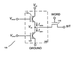
- FIG. 1 is a circuit diagram of a static random access memory (SRAM) cell consisting of the combination of two NDR-FET elements which form a bistable latch and one n-channel enhancement-mode IGFET access element;
- SRAM static random access memory
- FIG. 2 is a plot of the current-vs.-voltage characteristic of the bistable latch formed by the combination of two NDR-FETs as shown in FIG. 1 ;
- FIG. 3A is a top level view of a topology and layout for an SRAM cell of a first embodiment of an SRAM cell with reduced body effect, in which NDR-FET elements are connected and formed in common with an IGFET within a single p-type well;
- FIG. 3B is a top level view of a topology and layout for an SRAM cell of a second embodiment of an SRAM cell with reduced body effect, in which NDR-FET elements are connected and formed in a first p-type well, while an IGFET transfer element is formed within a separate second p-type well using triple-well process;
- FIG. 3C is a top level view of a topology and layout for an SRAM cell of a third embodiment of an SRAM cell with reduced body effect, in which one NDR-FET element is connected and formed in a first p-type well with an IGFET transfer element, while a second NDR FET element is formed within a separate second p-type well using a triple well process;
- FIGS. 4 and 4A are cross sectional and top views respectively of an exemplary SOI based NDR FET that can be used in an SRAM cell.
- FIG. 1 is a circuit diagram of a preferred embodiment of a static memory (SRAM) cell 100 consisting of two NDR elements 120 , 130 which form a bistable latch 140 and one enhancement-mode IGFET access element 110 .
- SRAM static memory
- FIG. 2 is a current-vs.-voltage plot illustrating the operational characteristics of the static memory cell 100 of FIG. 1 .
- NDR elements 120 , 130 of the present invention are preferably an NDR FET of the type referred to above in the aforementioned King et al. applications. The details of the same are provided for example in the aforementioned applications, and such documents are incorporated by reference herein primarily for the purpose of providing non-essential background information on representative types of environments in which the present inventions can be practiced. Other types of silicon based NDR FETs are clearly suitable and encompassed within the present teachings.
- the “body effect” is a well-known problem in memory (and other) applications in which the threshold voltage of a transistor (such as a pull up FET) is increased as a result of a logical high state being stored at a storage node V SN .
- a body to source p-n junction is reverse-biased.
- the body effect causes Vt of “pull-up” NDR FET 130 to be increased when data stored at node V SN is higher than V ss ; this increases the value of the gate bias (Vdd+Vt) required for the “pull-up” NDR FET 130 to maintain a high voltage (Vdd) at node V SN .
- the inventor has determined nonetheless that the body effect can be virtually eliminated in such embodiments by electrically floating the body of any NDR elements used within an SRAM, including NDR FETs 120 and 130 of an SRAM cell 100 shown in FIG. 1 .
- FIG. 3A a layout is optimized and made most compact by placing all of the elements (transistors in this case) in a single cell ( FIG. 1 ) within a single well.
- elements transistor in this case
- FIG. 3A like numeric designations are intended to denote like structures and features already depicted in FIG. 1 .
- FIG. 3A (and the other figures) is only intended to depict a small section of a representative memory array employing the present invention, and is not drawn to scale. The size, relationship and materials used for the structures shown in these figures may be altered significantly from that shown without departing from the present teachings.
- a single P type well (p-well) 360 is formed within an N type substrate 380 using conventional techniques as seen in FIG. 3 A.
- This p-well can be provided with a separate bias signal (WELL BIAS) at a well contact so that it can be biased or floated as is appropriate.
- WELL BIAS bias signal
- a cell 300 (1) highlighted in a hashed box includes an NDR pull-down element 320 with a source region 356 connected through a contact 318 to a ground or low reference potential Vss (the Vss line is not shown to avoid obscuring the invention) and an active region 357 forming a drain of NDR pull-down element 320 as well as a part of a storage node V SN .
- a bias line 354 provides a bias signal VB 1 to NDR pull-down element 320 , as well as to NDR pull-up element 330 .
- Active region 357 is also shared and acts as a source/drain region for NDR pull-up element 330 and a source/drain region for pass transistor 310 .
- a single doped region in well 360 is preferably used by three separate FETs (including a mixture of regular FETs and NDR based FETs) to increase the integration density of cell 300 .
- NDR pull-up element 330 also has a source/drain region 358 connected to a positive or high reference potential Vdd at contact 317 (the Vdd line is also not shown to avoid obscuring the invention).
- a word line WL 1 311 provides an activation signal for Read/Write operations in conventional fashion, and further acts as a gate for pass transistor 310 .
- a final source/drain region 314 for pass transistor 310 is connected to a Bit Line (again not shown to avoid obscuring the invention) through contact 316 for communicating data in and out of cell 300 .
- cell size is reduced by sharing Vdd contact regions, Vss contact regions, and Bit Line contact regions between adjacent memory cells;
- cell size is also reduced by forming both NDR and non-NDR elements with common regions within cell 300 , such as active region 357 ;
- processing complexity is reduced, because manufacturing operations for NDR and non-NDR elements are both effectuated using common CMOS techniques for isolation regions, active regions, gate insulators, gate interconnects, etc.
- the most compact 3-T SRAM layout shown in FIG. 3A has a cell size of 16F 2 , where F is the minimum feature size.
- F is the minimum feature size.
- This layout assumes that self-aligned, borderless contact process technology is available, and that the spacing between the NDR FETs and the regular FET can be minimal.
- the layout area is thus about 0.27 um 2 , which is about 11% as big as (or 9 ⁇ smaller than) a conventional 6-T SRAM. It should be noted that this is simply the smallest size available at this time given current processing techniques, and that other process improvements unforeseeable at this time to the inventor may yield additional cell size reductions.
- FIGS. 3B and 3C it may be desirable to only float the body of “pull-up” NDR FET 330 , or the body of both the NDR FETs 320 and 330 .
- like numerals in FIGS. 3B and 3C are intended to refer to like structures from FIGS. 1 and 3A . Again, those skilled in the art will understand that the structure shown in FIGS. 3B and 3C is only intended to depict a small section of a representative memory array employing the present invention.
- a well-known “triple-well” fabrication process is employed to provide separate body contacts and biasings for the NDR and non-NDR devices in an SRAM cell 300 . That is, pass transistor 310 is situated in a p-well 350 , while NDR FETs 320 and 330 are situated in a separate p-well 360 . The two wells are isolated by an isolation region 351 . P wells 350 and 360 are also commonly formed in an N-well 370 , and the latter is also itself situated within a further P well 380 . As formed, pass transistor 310 is connected to a word line 311 that forms also a gate electrode.
- a first source/drain region 314 is connected to a bit line 312 , while a second source/drain region 313 is connected and forms part of the storage node having a voltage V SN .
- pass transistor 310 is located entirely within P well 350 .
- Other pass transistors in the array can also be formed within P well 350 and use a single common well bias contact for a well bias signal WELL 1 BIAS.
- first NDR FET 320 includes an input bias line connected to a Vbias 1 input VB 1 , and also forming part of a gate electrode.
- a first reference low voltage supply source Vss is provided to a contact formed in a first source/drain region 356 .
- a second source/drain region 357 is shared with second NDR FET 330 , and is also coupled through an interconnect 359 to pass transistor 310 . This shared region also acts as part of the storage node V SN for SRAM cell 300 .
- Second NDR FET 330 includes an input bias line 354 connected to a Vbias 2 input, and which also forms part of a gate electrode.
- Vbias 1 and Vbias 2 are connected to the same signal supply through a common interconnect 354 .
- a second reference high voltage supply source Vdd is provided through a contact 317 which is coupled a third source/drain region 358 .
- both NDR FET 320 and NDR FET 330 are formed in a p-well 360 , which is separate from p-well 350 in which pass transistor 310 is formed.
- a bias signal WELL 1 BIAS can be applied to a contact coupled to p-well 360 as shown, or in some other form.
- separate body biasings can be provided to the different types of FETs (at respective contacts for WELL 1 BIAS and WELL 2 BIAS) in a single memory cell so that, for example, a body contact for NDR FETs 320 , 330 can be left floating to reduce body effects.
- NDR source/drain regions are shared within a cell, and adjacent cells also share common Vss and VDD contacts, and bit line contacts. Again it will be understood by those skilled in the art that separate well bias contacts may or may not be provided, and the figure is merely intended to facilitate understanding of the invention.
- only one of the NDR FETs is formed in a separate p-well 360 ; namely, pull-up NDR FET 330 .
- Such wells can be shared between adjacent cells and given separate bias contacts 390 as shown therein.
- FIGS. 3A , 3 B and 3 C are not intended to be to scale, and are not intended to describe every possible arrangement of the various structures and features therein.
- the location and relative size of the interconnect layers (between source/drain regions) has been altered to make the features of the invention more apparent.
- Many other features shown may vary in size, relationship or structure from that illustrated.
- Other supporting structures may also be incorporated within an SRAM cell 100 , including conventional NDR diodes.
- triple wells Standard techniques for forming triple wells are well-known, and any suitable process can be employed with the present invention to achieve the result of allowing separate body biasing of the various elements in SRAM cells. It will be noted, of course, that the layout in triple well embodiments is not as compact (as can be seen by comparing FIGS. 3A , 3 B and 3 C) because of required well-to-well spacings within a cell, but it may be necessary in some applications.
- SRAM bulk Silicon embodiments of the present invention can include one or more of the following variations to improve body effect performance:
- SOI devices differ from bulk Si devices primarily by the fact that in the former a buried oxide layer insulates a thin silicon layer body (for the active devices) from the bulk Si substrate.
- the active devices are patterned (typically) as mesas above the buried oxide layer. The process is somewhat less mature than regular bulk Si CMOS processes, but the result is a pattern of distinct and individual active devices isolated from each other by the insulator layer with superior leakage and parasitic performance over bulk Si for fine scaled geometries.
- SOI technology Two particular types of SOI technology that can be used with the present invention include: (1) partially depleted; (2) fully depleted implementations. These are not intended to be exhaustive, of course, and it will be understood by those skilled in the art that the present invention is not limited to these specific types of SOI technology.
- FIG. 4 illustrates a cross section of a typical SOI transistor 401 which, as explained herein, can also be configured as NDR capable FETs.
- Each transistor is formed on bulk silicon substrate 405 , and a buried oxide (insulator) layer 410 .
- Each transistor further includes a pair of N+ source/drain regions ( 415 , 425 ) doped N type (for an n channel device) and a body region 420 doped with a net P type concentration (as explained above for the bulk Si case).
- the source/drain ( 415 , 425 ) and body structures ( 425 ) are typically formed by a thin single-crystalline silicon film that is later patterned and etched to yield the resulting structures shown in FIG. 4.
- a gate insulating layer 430 includes a trapping region 437 (of the type described in the aforementioned King et al applications) for forming traps, and the net P type concentration in body 420 (also formed as explained in the aforementioned King et al applications) help provide a carrier trapping effect to create an NDR effect as noted in such applications.
- a gate contact 440 completes the device, and in most instances this is made of an N+ doped polycrystalline silicon material.
- An interconnect layer (not shown) contacts the NDR FET to provide an NDR bias signal of the type described earlier. It will be apparent that the as-shown SOI FET 401 can thus be adapted as an SOI NDR FET and incorporated for use in a memory cell 100 of the type shown in FIG. 1 .
- a separate body contact (and interconnect) 450 are provided for each transistor 401 , if body biasing is desired to operate in a non-floating body effect mode, because each transistor is fabricated in a separate “island” of SOI. It can be seen quite clearly (from for this single transistor case) that the layout area penalty for an array of such interconnected transistors configured for an SRAM is thus larger than for a bulk-Si technology in which many transistors can reside in a single well and body contact is provided to each of those transistors with a single well contact.
- the partially depleted (1) case refers to the situation where an SOI layer 420 (forming the body regions of the NDR and non-NDR FETs) is partially depleted for a transistor in the ON state.
- the well-known “floating body effect” associated with SOI transistors will cause the drain current to increase at high drain voltages, resulting in a “kink” in the Ids vs. Vds characteristic for a fixed gate voltage (Vg>Vt).
- the fully depleted case (2) refers to a condition in which the body region can be fully depleted for a transistor in the ON state.
- the “floating body effect” is negligible, because the holes generated by impact ionization in the high-field region near the drain can flow through the body into the source relatively easily.
- the potential barrier to hole flow into the source is very small, for a fully depleted body. The detrimental effect on PVR is therefore avoided.
Landscapes
- Engineering & Computer Science (AREA)
- Microelectronics & Electronic Packaging (AREA)
- Computer Hardware Design (AREA)
- Semiconductor Memories (AREA)
- Thin Film Transistor (AREA)
Abstract
Description
-
- i) body floating for all elements (including the three transistors as seen in FIG. 3A);
- ii) body floating for both NDR elements (as seen in FIG. 3B);
- iii) body floating for a “pull-up” (or load) NDR element only (as seen in
FIG. 3C )
Fourth Embodiment—SOI
Claims (8)
Priority Applications (2)
| Application Number | Priority Date | Filing Date | Title |
|---|---|---|---|
| US10/215,137 US6864104B2 (en) | 2002-06-28 | 2002-08-08 | Silicon on insulator (SOI) negative differential resistance (NDR) based memory device with reduced body effects |
| US11/035,786 US7187028B2 (en) | 2002-06-28 | 2005-01-13 | Silicon on insulator (SOI) negative differential resistance (NDR) based memory device with reduced body effects |
Applications Claiming Priority (2)
| Application Number | Priority Date | Filing Date | Title |
|---|---|---|---|
| US10/185,559 US6912151B2 (en) | 2002-06-28 | 2002-06-28 | Negative differential resistance (NDR) based memory device with reduced body effects |
| US10/215,137 US6864104B2 (en) | 2002-06-28 | 2002-08-08 | Silicon on insulator (SOI) negative differential resistance (NDR) based memory device with reduced body effects |
Related Parent Applications (1)
| Application Number | Title | Priority Date | Filing Date |
|---|---|---|---|
| US10/185,559 Continuation-In-Part US6912151B2 (en) | 2002-06-28 | 2002-06-28 | Negative differential resistance (NDR) based memory device with reduced body effects |
Related Child Applications (1)
| Application Number | Title | Priority Date | Filing Date |
|---|---|---|---|
| US11/035,786 Division US7187028B2 (en) | 2002-06-28 | 2005-01-13 | Silicon on insulator (SOI) negative differential resistance (NDR) based memory device with reduced body effects |
Publications (2)
| Publication Number | Publication Date |
|---|---|
| US20040008535A1 US20040008535A1 (en) | 2004-01-15 |
| US6864104B2 true US6864104B2 (en) | 2005-03-08 |
Family
ID=34636005
Family Applications (2)
| Application Number | Title | Priority Date | Filing Date |
|---|---|---|---|
| US10/215,137 Expired - Lifetime US6864104B2 (en) | 2002-06-28 | 2002-08-08 | Silicon on insulator (SOI) negative differential resistance (NDR) based memory device with reduced body effects |
| US11/035,786 Expired - Lifetime US7187028B2 (en) | 2002-06-28 | 2005-01-13 | Silicon on insulator (SOI) negative differential resistance (NDR) based memory device with reduced body effects |
Family Applications After (1)
| Application Number | Title | Priority Date | Filing Date |
|---|---|---|---|
| US11/035,786 Expired - Lifetime US7187028B2 (en) | 2002-06-28 | 2005-01-13 | Silicon on insulator (SOI) negative differential resistance (NDR) based memory device with reduced body effects |
Country Status (1)
| Country | Link |
|---|---|
| US (2) | US6864104B2 (en) |
Cited By (4)
| Publication number | Priority date | Publication date | Assignee | Title |
|---|---|---|---|---|
| US20050153461A1 (en) * | 2002-12-09 | 2005-07-14 | Progressant Technologies, Inc. | Process for controlling performance characteristics of a negative differential resistance (NDR) device |
| US20060231893A1 (en) * | 2005-04-15 | 2006-10-19 | International Business Machines Corporation | Hybrid crystal orientation CMOS structure for adaptive well biasing and for power and performance enhancement |
| US20070252212A1 (en) * | 2006-04-26 | 2007-11-01 | International Business Machines Corporation | Improved cmos diodes with dual gate conductors, and methods for forming the same |
| US20090212363A1 (en) * | 2008-02-27 | 2009-08-27 | Advanced Micro Devices, Inc. | Method for forming a one-transistor memory cell and related structure |
Families Citing this family (5)
| Publication number | Priority date | Publication date | Assignee | Title |
|---|---|---|---|---|
| US8125003B2 (en) * | 2003-07-02 | 2012-02-28 | Micron Technology, Inc. | High-performance one-transistor memory cell |
| US7508701B1 (en) * | 2006-11-29 | 2009-03-24 | The Board Of Trustees Of The Leland Stanford Junior University | Negative differential resistance devices and approaches therefor |
| US8723260B1 (en) * | 2009-03-12 | 2014-05-13 | Rf Micro Devices, Inc. | Semiconductor radio frequency switch with body contact |
| US8350338B2 (en) | 2011-02-08 | 2013-01-08 | International Business Machines Corporations | Semiconductor device including high field regions and related method |
| US20160093491A1 (en) * | 2014-09-29 | 2016-03-31 | University Of North Texas | LARGE SCALE AND THICKNESS-MODULATED MoS2 NANOSHEETS |
Citations (103)
| Publication number | Priority date | Publication date | Assignee | Title |
|---|---|---|---|---|
| US3588736A (en) | 1969-06-30 | 1971-06-28 | Ibm | Three-terminal bulk negative resistance device operable in oscillatory and bistable modes |
| US3903542A (en) | 1974-03-11 | 1975-09-02 | Westinghouse Electric Corp | Surface gate-induced conductivity modulated negative resistance semiconductor device |
| US3974486A (en) | 1975-04-07 | 1976-08-10 | International Business Machines Corporation | Multiplication mode bistable field effect transistor and memory utilizing same |
| US4047974A (en) | 1975-12-30 | 1977-09-13 | Hughes Aircraft Company | Process for fabricating non-volatile field effect semiconductor memory structure utilizing implanted ions to induce trapping states |
| US4143393A (en) | 1977-06-21 | 1979-03-06 | International Business Machines Corporation | High field capacitor structure employing a carrier trapping region |
| US4644386A (en) | 1982-06-29 | 1987-02-17 | Handotai Kenkyu Shinkokai | Integrated circuit employing insulated gate electrostatic induction transistor |
| US4806998A (en) | 1986-06-30 | 1989-02-21 | Thomson-Csf | Heterojunction and dual channel semiconductor field effect transistor or negative transconductive device |
| WO1990003646A1 (en) | 1988-09-30 | 1990-04-05 | Dallas Semiconductor Corporation | Integrated circuit with compact load elements |
| US4945393A (en) | 1988-06-21 | 1990-07-31 | At&T Bell Laboratories | Floating gate memory circuit and apparatus |
| US5021841A (en) | 1988-10-14 | 1991-06-04 | University Of Illinois | Semiconductor device with controlled negative differential resistance characteristic |
| US5023836A (en) | 1988-07-20 | 1991-06-11 | Fujitsu Limited | Semiconductor memory device |
| US5032891A (en) | 1989-05-17 | 1991-07-16 | Kabushiki Kaisha Toshiba | Semiconductor memory device and manufacturing method thereof |
| US5084743A (en) | 1990-03-15 | 1992-01-28 | North Carolina State University At Raleigh | High current, high voltage breakdown field effect transistor |
| US5093699A (en) | 1990-03-12 | 1992-03-03 | Texas A & M University System | Gate adjusted resonant tunnel diode device and method of manufacture |
| US5130763A (en) | 1989-01-24 | 1992-07-14 | U.S. Philips Corp. | Integrated semiconductor device with an insulated-gate field effect transistor having a negative transconductance zone |
| US5162880A (en) | 1989-09-27 | 1992-11-10 | Kabushiki Kaisha Toshiba | Nonvolatile memory cell having gate insulation film with carrier traps therein |
| US5189499A (en) | 1990-02-21 | 1993-02-23 | Sony Corporation | Charge-coupled device and process of fabrication thereof |
| US5357134A (en) | 1991-10-31 | 1994-10-18 | Rohm Co., Ltd. | Nonvolatile semiconductor device having charge trap film containing silicon crystal grains |
| US5390145A (en) | 1993-04-15 | 1995-02-14 | Fujitsu Limited | Resonance tunnel diode memory |
| US5442194A (en) | 1994-01-07 | 1995-08-15 | Texas Instruments Incorporated | Room-temperature tunneling hot-electron transistor |
| US5448513A (en) | 1993-12-02 | 1995-09-05 | Regents Of The University Of California | Capacitorless DRAM device on silicon-on-insulator substrate |
| US5455432A (en) | 1994-10-11 | 1995-10-03 | Kobe Steel Usa | Diamond semiconductor device with carbide interlayer |
| US5463234A (en) | 1992-03-31 | 1995-10-31 | Kabushiki Kaisha Toshiba | High-speed semiconductor gain memory cell with minimal area occupancy |
| US5477169A (en) | 1994-06-20 | 1995-12-19 | Motorola | Logic circuit with negative differential resistance device |
| US5523603A (en) | 1990-04-16 | 1996-06-04 | Digital Equipment Corporation | Semiconductor device with reduced time-dependent dielectric failures |
| US5543652A (en) | 1992-08-10 | 1996-08-06 | Hitachi, Ltd. | Semiconductor device having a two-channel MISFET arrangement defined by I-V characteristic having a negative resistance curve and SRAM cells employing the same |
| US5552622A (en) | 1992-07-14 | 1996-09-03 | Mitsuteru Kimura | Tunnel transistor |
| EP0747940A2 (en) | 1995-06-07 | 1996-12-11 | STMicroelectronics, Inc. | Fully-dielectric-isolated FET technology |
| EP0747961A2 (en) | 1995-06-07 | 1996-12-11 | STMicroelectronics, Inc. | Zero-power SRAM with patterned buried oxide isolation |
| US5606177A (en) | 1993-10-29 | 1997-02-25 | Texas Instruments Incorporated | Silicon oxide resonant tunneling diode structure |
| US5633178A (en) | 1993-11-29 | 1997-05-27 | Sgs-Thomson Microelectronics S.A. | Method of making volatile memory cell with interface charge traps |
| US5689458A (en) | 1995-06-08 | 1997-11-18 | Mitsubishi Denki Kabushiki Kaisha | Semiconductor memory device having negative resistance element operated stably with single low power source |
| US5698997A (en) | 1995-09-28 | 1997-12-16 | Mayo Foundation For Medical Education And Research | Resonant tunneling diode structures for functionally complete low power logic |
| US5705827A (en) | 1991-12-25 | 1998-01-06 | Nec Corporation | Tunnel transistor and method of manufacturing same |
| US5732014A (en) | 1997-02-20 | 1998-03-24 | Micron Technology, Inc. | Merged transistor structure for gain memory cell |
| US5761114A (en) | 1997-02-19 | 1998-06-02 | International Business Machines Corporation | Multi-level storage gain cell with stepline |
| US5770958A (en) | 1996-04-04 | 1998-06-23 | Nippon Telegraph And Telephone Corporation | Periodic waveform generating circuit |
| US5773996A (en) | 1995-05-22 | 1998-06-30 | Nippon Telegraph And Telephone Corporation | Multiple-valued logic circuit |
| US5798965A (en) | 1996-04-12 | 1998-08-25 | Lg Semicon Co., Ltd. | Dynamic random access memory having no capacitor and method for fabricating the same |
| US5804475A (en) | 1994-11-14 | 1998-09-08 | The United States Of America As Represented By The Secretary Of The Navy | Method of forming an interband lateral resonant tunneling transistor |
| US5843812A (en) | 1993-10-28 | 1998-12-01 | Goldstar Electron Co., Ltd. | Method of making a PMOSFET in a semiconductor device |
| US5869845A (en) | 1997-06-26 | 1999-02-09 | Texas Instruments Incorporated | Resonant tunneling memory |
| US5883549A (en) | 1997-06-20 | 1999-03-16 | Hughes Electronics Corporation | Bipolar junction transistor (BJT)--resonant tunneling diode (RTD) oscillator circuit and method |
| US5883829A (en) | 1997-06-27 | 1999-03-16 | Texas Instruments Incorporated | Memory cell having negative differential resistance devices |
| US5895934A (en) | 1997-08-13 | 1999-04-20 | The United States Of America As Represented By The Secretary Of The Army | Negative differential resistance device based on tunneling through microclusters, and method therefor |
| US5903170A (en) | 1997-06-03 | 1999-05-11 | The Regents Of The University Of Michigan | Digital logic design using negative differential resistance diodes and field-effect transistors |
| US5907159A (en) | 1996-11-05 | 1999-05-25 | Electronics And Telecommunications Research Institute | Hot electron device and a resonant tunneling hot electron device |
| US5936265A (en) | 1996-03-25 | 1999-08-10 | Kabushiki Kaisha Toshiba | Semiconductor device including a tunnel effect element |
| US5945706A (en) | 1990-10-21 | 1999-08-31 | Lg Semicon Co., Ltd. | Memory device |
| US5959328A (en) | 1996-01-08 | 1999-09-28 | Siemens Aktiengesellschaft | Electrically programmable memory cell arrangement and method for its manufacture |
| US5962864A (en) | 1996-08-16 | 1999-10-05 | Kabushiki Kaisha Toshiba | Gated resonant tunneling device and fabricating method thereof |
| WO1999063598A1 (en) | 1998-06-05 | 1999-12-09 | Stanford University | Semiconductor current-switching device having operational enhancer and method therefor |
| US6015739A (en) | 1997-10-29 | 2000-01-18 | Advanced Micro Devices | Method of making gate dielectric for sub-half micron MOS transistors including a graded dielectric constant |
| US6015978A (en) | 1996-03-01 | 2000-01-18 | Matsushita Electric Industrial Co., Ltd. | Resonance tunnel device |
| US6075265A (en) | 1997-06-27 | 2000-06-13 | Siemens Aktiengesellschaft | DRAM cell arrangement and method for its fabrication |
| US6077760A (en) | 1997-09-04 | 2000-06-20 | National Science Council | Structure and method of manufacturing single-crystal silicon carbide/single-crystal silicon heterojunctions with negative differential resistance characteristics |
| US6084796A (en) | 1996-05-30 | 2000-07-04 | Axon Technologies Corporation | Programmable metallization cell structure and method of making same |
| WO2000041309A1 (en) | 1999-01-06 | 2000-07-13 | Raytheon Company | Method and system for quantizing an analog signal utilizing a clocked resonant tunneling diode pair |
| US6091077A (en) | 1996-10-22 | 2000-07-18 | Matsushita Electric Industrial Co., Ltd. | MIS SOI semiconductor device with RTD and/or HET |
| US6097036A (en) | 1995-03-08 | 2000-08-01 | Hitachi, Llp | Semiconductor logic element and apparatus using thereof |
| US6104631A (en) | 1997-12-17 | 2000-08-15 | National Scientific Corp. | Static memory cell with load circuit using a tunnel diode |
| US6128216A (en) | 1998-05-13 | 2000-10-03 | Micron Technology Inc. | High density planar SRAM cell with merged transistors |
| US6130559A (en) | 1997-04-04 | 2000-10-10 | Board Of Regents Of The University Of Texas System | QMOS digital logic circuits |
| EP1050964A2 (en) | 1999-04-28 | 2000-11-08 | Nec Corporation | Flip-flop circuit |
| US6150242A (en) | 1998-03-25 | 2000-11-21 | Texas Instruments Incorporated | Method of growing crystalline silicon overlayers on thin amorphous silicon oxide layers and forming by method a resonant tunneling diode |
| EP1065656A2 (en) | 1994-05-13 | 2001-01-03 | Sony Corporation | Method for reducing noise in an input speech signal |
| US6184539B1 (en) | 1996-11-12 | 2001-02-06 | Micron Technology, Inc. | Static memory cell and method of forming static memory cell |
| US6205054B1 (en) | 1998-12-14 | 2001-03-20 | Global Alliance Inc. | Nonvolatile memory |
| US6222766B1 (en) | 1999-01-12 | 2001-04-24 | International Business Machiness Corporation | EEPROM memory cell and method of fabricating the same |
| US6225165B1 (en) | 1998-05-13 | 2001-05-01 | Micron Technology, Inc. | High density SRAM cell with latched vertical transistors |
| US6246606B1 (en) | 1997-11-13 | 2001-06-12 | Micron Technology, Inc. | Memory using insulator traps |
| EP1107317A1 (en) | 1999-12-09 | 2001-06-13 | Hitachi Europe Limited | Memory device |
| US20010005327A1 (en) | 1999-12-22 | 2001-06-28 | Russell Duane | Negative resistance device |
| US20010019137A1 (en) | 2000-03-06 | 2001-09-06 | Kabushiki Toshiba | Semiconductor device and method of manufacturing the same |
| WO2001065597A1 (en) | 2000-02-29 | 2001-09-07 | Motorola, Inc. | Semiconductor device and method of fabrication |
| WO2001069607A2 (en) | 2000-03-14 | 2001-09-20 | Motorola, Inc. | Memory cell, method of formation, and operation |
| US6294412B1 (en) | 2000-06-09 | 2001-09-25 | Advanced Micro Devices | Silicon based lateral tunneling memory cell |
| US20010024841A1 (en) | 1998-05-13 | 2001-09-27 | Noble Wendell P. | High density vertical sram cell using bipolar latchup induced by gated diode breakdown |
| US6301147B1 (en) | 1997-12-17 | 2001-10-09 | National Scientific Corporation | Electronic semiconductor circuit which includes a tunnel diode |
| US6303942B1 (en) | 1998-03-17 | 2001-10-16 | Farmer, Ii Kenneth Rudolph | Multi-layer charge injection barrier and uses thereof |
| EP0526897B1 (en) | 1991-08-06 | 2001-11-07 | Nec Corporation | Three terminal tunnel device |
| WO2001088977A2 (en) | 2000-05-18 | 2001-11-22 | Infineon Technologies North America Corp. | Method and device for array threshold voltage control by trapped charge in trench isolation |
| US20010053568A1 (en) | 1998-09-24 | 2001-12-20 | Gerald Deboy | Method for manufacturing a semiconductor component |
| WO2001099153A2 (en) | 2000-06-22 | 2001-12-27 | Progressant Technologies, Inc. | A negative differential resistance device and method of operating same |
| US20020017681A1 (en) | 2000-07-11 | 2002-02-14 | Seiko Epson Corporation | Semiconductor device and method of manufacture |
| US6353251B1 (en) | 1997-11-28 | 2002-03-05 | Mitsuteru Kimura | MOS gate Schottky tunnel transistor and an integrated circuit using the same |
| US20020048190A1 (en) | 2000-06-22 | 2002-04-25 | Tsu-Jae King | Insulated-gate field-effect transistor integrated with negative differential resistance (NDR) FET |
| EP1204146A1 (en) | 1993-08-19 | 2002-05-08 | Hitachi, Ltd. | Semiconductor element and semiconductor memory device using the same |
| US20020054502A1 (en) | 2000-06-22 | 2002-05-09 | Tsu-Jae King | Memory cell using negative differential resistance field effect transistors |
| US20020057123A1 (en) | 2000-06-22 | 2002-05-16 | Tsu-Jae King | Dual mode fet & logic circuit having negative differential resistance mode |
| US6396731B1 (en) | 2001-03-30 | 2002-05-28 | Taiwan Semiconductor Manufacturing Company, Ltd | SRAM cell employing tunnel switched diode |
| US20020063277A1 (en) | 2000-11-28 | 2002-05-30 | Ramsbey Mark T. | Planar structure for non-volatile memory devices |
| US20020067651A1 (en) | 2000-06-22 | 2002-06-06 | King Tsu-Jae | Charge pump for negative differential resistance transistor |
| US20020066933A1 (en) | 2000-06-22 | 2002-06-06 | King Tsu-Jae | Negative differential resistance field effect transistor (NDR-FET) & circuits using the same |
| US6404018B1 (en) | 1995-06-21 | 2002-06-11 | Micron Technology, Inc. | Static memory cell and method of manufacturing a static memory cell |
| US20020076850A1 (en) | 2000-12-19 | 2002-06-20 | Sadd Michael A. | Device structure for storing charge and method therefore |
| US20020093030A1 (en) | 2001-01-16 | 2002-07-18 | International Business Machines Corporation | T-RAM array having a planar cell structure and method for fabricating the same |
| US6424174B1 (en) | 2001-10-17 | 2002-07-23 | International Business Machines Corporation | Low leakage logic gates |
| US20020096723A1 (en) | 1999-12-31 | 2002-07-25 | Kaoru Awaka | Transient frequency in dynamic threshold metal-oxide-semiconductor field effect transistors |
| US20020100918A1 (en) | 2001-01-26 | 2002-08-01 | Hsu Louis L. | T-RAM array having a planar cell structure and method for fabricating the same |
| US20020109150A1 (en) | 2001-02-13 | 2002-08-15 | Kabushiki Kaisha Toshiba | Semiconductor device and manufacturing method thereof |
| US6448161B1 (en) | 2000-06-09 | 2002-09-10 | Advanced Micro Devices, Inc. | Silicon based vertical tunneling memory cell |
| EP1251562A1 (en) | 2001-04-20 | 2002-10-23 | Btg International Limited | Nanoelectronic devices and circuits |
Family Cites Families (4)
| Publication number | Priority date | Publication date | Assignee | Title |
|---|---|---|---|---|
| JP3444727B2 (en) * | 1995-09-26 | 2003-09-08 | シャープ株式会社 | Digital satellite broadcasting receiver |
| US6366134B1 (en) | 1999-09-16 | 2002-04-02 | Texas Instruments Incorporated | CMOS dynamic logic circuitry using quantum mechanical tunneling structures |
| CN1190964C (en) * | 2000-02-14 | 2005-02-23 | 夏普公司 | Tuner of cable modem |
| US6912151B2 (en) * | 2002-06-28 | 2005-06-28 | Synopsys, Inc. | Negative differential resistance (NDR) based memory device with reduced body effects |
-
2002
- 2002-08-08 US US10/215,137 patent/US6864104B2/en not_active Expired - Lifetime
-
2005
- 2005-01-13 US US11/035,786 patent/US7187028B2/en not_active Expired - Lifetime
Patent Citations (109)
| Publication number | Priority date | Publication date | Assignee | Title |
|---|---|---|---|---|
| US3588736A (en) | 1969-06-30 | 1971-06-28 | Ibm | Three-terminal bulk negative resistance device operable in oscillatory and bistable modes |
| US3903542A (en) | 1974-03-11 | 1975-09-02 | Westinghouse Electric Corp | Surface gate-induced conductivity modulated negative resistance semiconductor device |
| US3974486A (en) | 1975-04-07 | 1976-08-10 | International Business Machines Corporation | Multiplication mode bistable field effect transistor and memory utilizing same |
| US4047974A (en) | 1975-12-30 | 1977-09-13 | Hughes Aircraft Company | Process for fabricating non-volatile field effect semiconductor memory structure utilizing implanted ions to induce trapping states |
| US4143393A (en) | 1977-06-21 | 1979-03-06 | International Business Machines Corporation | High field capacitor structure employing a carrier trapping region |
| US4644386A (en) | 1982-06-29 | 1987-02-17 | Handotai Kenkyu Shinkokai | Integrated circuit employing insulated gate electrostatic induction transistor |
| US4806998A (en) | 1986-06-30 | 1989-02-21 | Thomson-Csf | Heterojunction and dual channel semiconductor field effect transistor or negative transconductive device |
| US4945393A (en) | 1988-06-21 | 1990-07-31 | At&T Bell Laboratories | Floating gate memory circuit and apparatus |
| US5023836A (en) | 1988-07-20 | 1991-06-11 | Fujitsu Limited | Semiconductor memory device |
| WO1990003646A1 (en) | 1988-09-30 | 1990-04-05 | Dallas Semiconductor Corporation | Integrated circuit with compact load elements |
| US5021841A (en) | 1988-10-14 | 1991-06-04 | University Of Illinois | Semiconductor device with controlled negative differential resistance characteristic |
| US5130763A (en) | 1989-01-24 | 1992-07-14 | U.S. Philips Corp. | Integrated semiconductor device with an insulated-gate field effect transistor having a negative transconductance zone |
| US5032891A (en) | 1989-05-17 | 1991-07-16 | Kabushiki Kaisha Toshiba | Semiconductor memory device and manufacturing method thereof |
| US5162880A (en) | 1989-09-27 | 1992-11-10 | Kabushiki Kaisha Toshiba | Nonvolatile memory cell having gate insulation film with carrier traps therein |
| US5189499A (en) | 1990-02-21 | 1993-02-23 | Sony Corporation | Charge-coupled device and process of fabrication thereof |
| US5093699A (en) | 1990-03-12 | 1992-03-03 | Texas A & M University System | Gate adjusted resonant tunnel diode device and method of manufacture |
| US5084743A (en) | 1990-03-15 | 1992-01-28 | North Carolina State University At Raleigh | High current, high voltage breakdown field effect transistor |
| US5523603A (en) | 1990-04-16 | 1996-06-04 | Digital Equipment Corporation | Semiconductor device with reduced time-dependent dielectric failures |
| US5945706A (en) | 1990-10-21 | 1999-08-31 | Lg Semicon Co., Ltd. | Memory device |
| EP0526897B1 (en) | 1991-08-06 | 2001-11-07 | Nec Corporation | Three terminal tunnel device |
| US5357134A (en) | 1991-10-31 | 1994-10-18 | Rohm Co., Ltd. | Nonvolatile semiconductor device having charge trap film containing silicon crystal grains |
| US5705827A (en) | 1991-12-25 | 1998-01-06 | Nec Corporation | Tunnel transistor and method of manufacturing same |
| US5463234A (en) | 1992-03-31 | 1995-10-31 | Kabushiki Kaisha Toshiba | High-speed semiconductor gain memory cell with minimal area occupancy |
| US5552622A (en) | 1992-07-14 | 1996-09-03 | Mitsuteru Kimura | Tunnel transistor |
| US5543652A (en) | 1992-08-10 | 1996-08-06 | Hitachi, Ltd. | Semiconductor device having a two-channel MISFET arrangement defined by I-V characteristic having a negative resistance curve and SRAM cells employing the same |
| US5390145A (en) | 1993-04-15 | 1995-02-14 | Fujitsu Limited | Resonance tunnel diode memory |
| EP1204146A1 (en) | 1993-08-19 | 2002-05-08 | Hitachi, Ltd. | Semiconductor element and semiconductor memory device using the same |
| US5843812A (en) | 1993-10-28 | 1998-12-01 | Goldstar Electron Co., Ltd. | Method of making a PMOSFET in a semiconductor device |
| US5606177A (en) | 1993-10-29 | 1997-02-25 | Texas Instruments Incorporated | Silicon oxide resonant tunneling diode structure |
| US5633178A (en) | 1993-11-29 | 1997-05-27 | Sgs-Thomson Microelectronics S.A. | Method of making volatile memory cell with interface charge traps |
| EP0655788B1 (en) | 1993-11-29 | 1998-01-21 | STMicroelectronics S.A. | A volatile memory cell |
| US5448513A (en) | 1993-12-02 | 1995-09-05 | Regents Of The University Of California | Capacitorless DRAM device on silicon-on-insulator substrate |
| US5442194A (en) | 1994-01-07 | 1995-08-15 | Texas Instruments Incorporated | Room-temperature tunneling hot-electron transistor |
| EP1065656A2 (en) | 1994-05-13 | 2001-01-03 | Sony Corporation | Method for reducing noise in an input speech signal |
| US5477169A (en) | 1994-06-20 | 1995-12-19 | Motorola | Logic circuit with negative differential resistance device |
| US5455432A (en) | 1994-10-11 | 1995-10-03 | Kobe Steel Usa | Diamond semiconductor device with carbide interlayer |
| US5804475A (en) | 1994-11-14 | 1998-09-08 | The United States Of America As Represented By The Secretary Of The Navy | Method of forming an interband lateral resonant tunneling transistor |
| US6097036A (en) | 1995-03-08 | 2000-08-01 | Hitachi, Llp | Semiconductor logic element and apparatus using thereof |
| US5773996A (en) | 1995-05-22 | 1998-06-30 | Nippon Telegraph And Telephone Corporation | Multiple-valued logic circuit |
| EP0747961A2 (en) | 1995-06-07 | 1996-12-11 | STMicroelectronics, Inc. | Zero-power SRAM with patterned buried oxide isolation |
| EP0747940A2 (en) | 1995-06-07 | 1996-12-11 | STMicroelectronics, Inc. | Fully-dielectric-isolated FET technology |
| US5689458A (en) | 1995-06-08 | 1997-11-18 | Mitsubishi Denki Kabushiki Kaisha | Semiconductor memory device having negative resistance element operated stably with single low power source |
| US6404018B1 (en) | 1995-06-21 | 2002-06-11 | Micron Technology, Inc. | Static memory cell and method of manufacturing a static memory cell |
| US5698997A (en) | 1995-09-28 | 1997-12-16 | Mayo Foundation For Medical Education And Research | Resonant tunneling diode structures for functionally complete low power logic |
| US5959328A (en) | 1996-01-08 | 1999-09-28 | Siemens Aktiengesellschaft | Electrically programmable memory cell arrangement and method for its manufacture |
| US6015978A (en) | 1996-03-01 | 2000-01-18 | Matsushita Electric Industrial Co., Ltd. | Resonance tunnel device |
| US5936265A (en) | 1996-03-25 | 1999-08-10 | Kabushiki Kaisha Toshiba | Semiconductor device including a tunnel effect element |
| US5770958A (en) | 1996-04-04 | 1998-06-23 | Nippon Telegraph And Telephone Corporation | Periodic waveform generating circuit |
| US5798965A (en) | 1996-04-12 | 1998-08-25 | Lg Semicon Co., Ltd. | Dynamic random access memory having no capacitor and method for fabricating the same |
| US6261896B1 (en) | 1996-05-16 | 2001-07-17 | Hyundai Electronics Industries Co., Ltd. | Memory device and method of forming the same |
| US6084796A (en) | 1996-05-30 | 2000-07-04 | Axon Technologies Corporation | Programmable metallization cell structure and method of making same |
| US5962864A (en) | 1996-08-16 | 1999-10-05 | Kabushiki Kaisha Toshiba | Gated resonant tunneling device and fabricating method thereof |
| US6091077A (en) | 1996-10-22 | 2000-07-18 | Matsushita Electric Industrial Co., Ltd. | MIS SOI semiconductor device with RTD and/or HET |
| US5907159A (en) | 1996-11-05 | 1999-05-25 | Electronics And Telecommunications Research Institute | Hot electron device and a resonant tunneling hot electron device |
| US6184539B1 (en) | 1996-11-12 | 2001-02-06 | Micron Technology, Inc. | Static memory cell and method of forming static memory cell |
| US5761114A (en) | 1997-02-19 | 1998-06-02 | International Business Machines Corporation | Multi-level storage gain cell with stepline |
| US5732014A (en) | 1997-02-20 | 1998-03-24 | Micron Technology, Inc. | Merged transistor structure for gain memory cell |
| US6130559A (en) | 1997-04-04 | 2000-10-10 | Board Of Regents Of The University Of Texas System | QMOS digital logic circuits |
| US5903170A (en) | 1997-06-03 | 1999-05-11 | The Regents Of The University Of Michigan | Digital logic design using negative differential resistance diodes and field-effect transistors |
| US5883549A (en) | 1997-06-20 | 1999-03-16 | Hughes Electronics Corporation | Bipolar junction transistor (BJT)--resonant tunneling diode (RTD) oscillator circuit and method |
| US5869845A (en) | 1997-06-26 | 1999-02-09 | Texas Instruments Incorporated | Resonant tunneling memory |
| US6075265A (en) | 1997-06-27 | 2000-06-13 | Siemens Aktiengesellschaft | DRAM cell arrangement and method for its fabrication |
| US5953249A (en) | 1997-06-27 | 1999-09-14 | Texas Instruments Incorporated | Memory cell having negative differential resistance devices |
| US5883829A (en) | 1997-06-27 | 1999-03-16 | Texas Instruments Incorporated | Memory cell having negative differential resistance devices |
| US5895934A (en) | 1997-08-13 | 1999-04-20 | The United States Of America As Represented By The Secretary Of The Army | Negative differential resistance device based on tunneling through microclusters, and method therefor |
| US6077760A (en) | 1997-09-04 | 2000-06-20 | National Science Council | Structure and method of manufacturing single-crystal silicon carbide/single-crystal silicon heterojunctions with negative differential resistance characteristics |
| US6015739A (en) | 1997-10-29 | 2000-01-18 | Advanced Micro Devices | Method of making gate dielectric for sub-half micron MOS transistors including a graded dielectric constant |
| US6246606B1 (en) | 1997-11-13 | 2001-06-12 | Micron Technology, Inc. | Memory using insulator traps |
| US6353251B1 (en) | 1997-11-28 | 2002-03-05 | Mitsuteru Kimura | MOS gate Schottky tunnel transistor and an integrated circuit using the same |
| US6301147B1 (en) | 1997-12-17 | 2001-10-09 | National Scientific Corporation | Electronic semiconductor circuit which includes a tunnel diode |
| US6104631A (en) | 1997-12-17 | 2000-08-15 | National Scientific Corp. | Static memory cell with load circuit using a tunnel diode |
| US6303942B1 (en) | 1998-03-17 | 2001-10-16 | Farmer, Ii Kenneth Rudolph | Multi-layer charge injection barrier and uses thereof |
| US6150242A (en) | 1998-03-25 | 2000-11-21 | Texas Instruments Incorporated | Method of growing crystalline silicon overlayers on thin amorphous silicon oxide layers and forming by method a resonant tunneling diode |
| US6225165B1 (en) | 1998-05-13 | 2001-05-01 | Micron Technology, Inc. | High density SRAM cell with latched vertical transistors |
| US6128216A (en) | 1998-05-13 | 2000-10-03 | Micron Technology Inc. | High density planar SRAM cell with merged transistors |
| US20010024841A1 (en) | 1998-05-13 | 2001-09-27 | Noble Wendell P. | High density vertical sram cell using bipolar latchup induced by gated diode breakdown |
| WO1999063598A1 (en) | 1998-06-05 | 1999-12-09 | Stanford University | Semiconductor current-switching device having operational enhancer and method therefor |
| US20010053568A1 (en) | 1998-09-24 | 2001-12-20 | Gerald Deboy | Method for manufacturing a semiconductor component |
| US6205054B1 (en) | 1998-12-14 | 2001-03-20 | Global Alliance Inc. | Nonvolatile memory |
| WO2000041309A1 (en) | 1999-01-06 | 2000-07-13 | Raytheon Company | Method and system for quantizing an analog signal utilizing a clocked resonant tunneling diode pair |
| US6222766B1 (en) | 1999-01-12 | 2001-04-24 | International Business Machiness Corporation | EEPROM memory cell and method of fabricating the same |
| EP1050964A2 (en) | 1999-04-28 | 2000-11-08 | Nec Corporation | Flip-flop circuit |
| EP1107317A1 (en) | 1999-12-09 | 2001-06-13 | Hitachi Europe Limited | Memory device |
| US20010013621A1 (en) | 1999-12-09 | 2001-08-16 | Kazuo Nakazato | Memory Device |
| US20010005327A1 (en) | 1999-12-22 | 2001-06-28 | Russell Duane | Negative resistance device |
| US6310799B2 (en) | 1999-12-22 | 2001-10-30 | National University Of Ireland, Cork | Negative resistance device |
| US20020096723A1 (en) | 1999-12-31 | 2002-07-25 | Kaoru Awaka | Transient frequency in dynamic threshold metal-oxide-semiconductor field effect transistors |
| WO2001065597A1 (en) | 2000-02-29 | 2001-09-07 | Motorola, Inc. | Semiconductor device and method of fabrication |
| US20010019137A1 (en) | 2000-03-06 | 2001-09-06 | Kabushiki Toshiba | Semiconductor device and method of manufacturing the same |
| WO2001069607A2 (en) | 2000-03-14 | 2001-09-20 | Motorola, Inc. | Memory cell, method of formation, and operation |
| WO2001088977A2 (en) | 2000-05-18 | 2001-11-22 | Infineon Technologies North America Corp. | Method and device for array threshold voltage control by trapped charge in trench isolation |
| US6448161B1 (en) | 2000-06-09 | 2002-09-10 | Advanced Micro Devices, Inc. | Silicon based vertical tunneling memory cell |
| US6294412B1 (en) | 2000-06-09 | 2001-09-25 | Advanced Micro Devices | Silicon based lateral tunneling memory cell |
| US20020054502A1 (en) | 2000-06-22 | 2002-05-09 | Tsu-Jae King | Memory cell using negative differential resistance field effect transistors |
| WO2001099153A2 (en) | 2000-06-22 | 2001-12-27 | Progressant Technologies, Inc. | A negative differential resistance device and method of operating same |
| US20020057123A1 (en) | 2000-06-22 | 2002-05-16 | Tsu-Jae King | Dual mode fet & logic circuit having negative differential resistance mode |
| EP1168456A2 (en) | 2000-06-22 | 2002-01-02 | Progressant Technologies Inc. | A CMOS-process compatible, tunable NDR (negative differential resistance) device and method of operating same |
| US20020067651A1 (en) | 2000-06-22 | 2002-06-06 | King Tsu-Jae | Charge pump for negative differential resistance transistor |
| US20020066933A1 (en) | 2000-06-22 | 2002-06-06 | King Tsu-Jae | Negative differential resistance field effect transistor (NDR-FET) & circuits using the same |
| US20020048190A1 (en) | 2000-06-22 | 2002-04-25 | Tsu-Jae King | Insulated-gate field-effect transistor integrated with negative differential resistance (NDR) FET |
| US20020017681A1 (en) | 2000-07-11 | 2002-02-14 | Seiko Epson Corporation | Semiconductor device and method of manufacture |
| US20020063277A1 (en) | 2000-11-28 | 2002-05-30 | Ramsbey Mark T. | Planar structure for non-volatile memory devices |
| US20020076850A1 (en) | 2000-12-19 | 2002-06-20 | Sadd Michael A. | Device structure for storing charge and method therefore |
| US20020093030A1 (en) | 2001-01-16 | 2002-07-18 | International Business Machines Corporation | T-RAM array having a planar cell structure and method for fabricating the same |
| US20020100918A1 (en) | 2001-01-26 | 2002-08-01 | Hsu Louis L. | T-RAM array having a planar cell structure and method for fabricating the same |
| US20020109150A1 (en) | 2001-02-13 | 2002-08-15 | Kabushiki Kaisha Toshiba | Semiconductor device and manufacturing method thereof |
| US6396731B1 (en) | 2001-03-30 | 2002-05-28 | Taiwan Semiconductor Manufacturing Company, Ltd | SRAM cell employing tunnel switched diode |
| EP1251562A1 (en) | 2001-04-20 | 2002-10-23 | Btg International Limited | Nanoelectronic devices and circuits |
| US6424174B1 (en) | 2001-10-17 | 2002-07-23 | International Business Machines Corporation | Low leakage logic gates |
Non-Patent Citations (59)
| Title |
|---|
| Barlow, P. S. et al., "Negative differential output conductance of self-heated power MOSFETs," IEE Proceedings-I Solid-State and Electron Devices, vol. 133, Part I, No. 5, Oct. 1986, pp. 177-179. |
| Believed to be published in: Deen, Jamal (editor) et al., excerpt from "CMOS RF modeling, characterization and applications," World Scientific, Apr. 2002, 34 pages. |
| Chan, E. et al., "Compact Multiple-Valued Multiplexers Using Negative Differential Resistance Devices," IEEE Journal of Solid-State Circuits, vol. 31, No. 8, Aug. 1996, pp. 1151-1156. |
| Chan, E. et al., "Mask Programmable Multi-Valued Logic Gate Using Resonant Tunnelling Diodes," IEE Proceedings-Circuits Devices Syst., vol. 143, No. 5, Oct. 1996, pp. 289-294. |
| Dozsa, L. et al., "A transient method for measuring current-voltage characteristics with negative differential resistance regions," Research Institute for Technical Physics, P. O. Box 76, H-1325 Budapest, Hungary, (Received Jul. 24, 1997; accepted Aug. 1, 1997), 2 pages. |
| Final Report: SMILE MEL-ARI Project n 28741-Chapter V, pp. 184-194. |
| Gardner, C. et al., "Smooth Quantum Hydrodynamic Model Simulation of the Resonant Tunneling Diode," Dept. of Mathematics Arizona State University, pp. 1-5, (1998). |
| Geppert, Linda, "Quantum transistors: toward nanoelectronics," IEEE Spectrum, Sep. 2000, pp. 46-51. |
| Goldhaber-Gordon, David et al., "Overview of nanoelectronic devices," Proc. IEEE, 85(4), Apr. 1997, pp. 521-540. |
| Gonzalez, A. et al., "Standard CMOS Implementation of a Multiple-Valued Logic Signed-Digit Adder Based on Negative Differential-Resistance Devices," Proceedings of the 30th IEEE International Symposium on Multiple-Valued Logic (ISMVL 2000), 6 pages. |
| Haddab, Y. et al., "Quantized current jumps in silicon photoconductors at room temperature," J. Appl. Phys. 86 (7), Oct. 1, 1999, pp. 3787-3791. |
| Haddad, G. I. et al., "Tunneling Devices and Applications in High Functionality/Speed Digital Circuits," Solid State Electronics, vol. 41, No. 10, Oct. 1997, pp. 1515-1524. |
| Hansch, W. et al., "The planar-doped-barrier-FET: MOSFET overcomes conventional limitations," ESSDERC'97 27th European Solid-State Device Research Conference, Stuttgart, Sep. 22-24, 1997, 4 pages. |
| Heij, C. P. et al., "Negative Differential Resistance Due to Single-Electron Switching," Applied Physics Letters, vol. 74, No. 7, Feb. 15, 1999, 5 pages. |
| Hong, J.W. et al., "Local charge trapping and detection of trapped charge by scanning capacitance microscope in SIO2/SI system," Appl. Phys. Lett., 75 (12), Sept. 20, 1999, pp. 1760-1762. |
| Jungel, A. et al., "Numerical Simulation of Semiconductor Devices: Energy-Transport and Quantum Hydrodynamic Modeling," Fachbereich Math., Tech. Univ. Berlin, Germany, pp. 1-9, 1998. |
| Karna, Shashi P. et al., "Point defects in SI-SI02 systems: current understanding," Published in G. Pacchioni et al. (eds.), "Defects in SIO2 and related dielectrics: science and technology," Kluwer Academic Publishers, (2000), 19 pages. |
| King, Tsu-Jae et al., U.S. Appl. No. 09/602,658, entitled "CMOS Compatible Process for Making a Tunable Negative Differential Resistance (NDR) Device," filed Jun. 22, 2000, 33 pages. |
| King, Tsu-Jae et al., U.S. Appl. No. 09/603,101 entitled "CMOS-Process Compatible, Tunable NDR (Negative Differential Resistance) Device and Method of Operating Same," filed Jun. 22, 2000, 34 pages. |
| King, Tsu-Jae et al., U.S. Appl. No. 09/603,102, entitled "Charge Trapping Device and Method for Implementing a Transistor having a Negative Differential Resistance Mode," filed Jun. 22, 2000, 39 pages. |
| Koester, S. J. et al., "Negative Differential Conductance in Lateral Double-Barrier Transistors Fabricated in Strained SI Quantum Wells," Applied Physics Letters, vol. 70, No. 18, May, 1997, pp. 2422-2424. |
| Luryi, S. et al., "Collector-Controlled States and the Formation of Hot Electron Domains in Real-Space Transfer Transistors," AT&T Bell Laboatories, p. 1-7, 1992. |
| Luryi, S. et al., "Collector-Controlled States in Charge Injection Transistors," SPIE-92 Symposium, pp. 1-12, 1992. |
| Luryi, S. et al., "Light-emitting Logic Devices based on Real Space Transfer in Complementary In GaAs/InAIAs Heterostructures", In "Negative Differential Resistance and Instabilities in 2D Semiconductors", ed. by N. Balkan, B. K. Ridley, and A. J. Vickers, NATO ASI Series [Physics] B 307, pp. 53-82, Planum Press (New York 1993). |
| Mathews, R. H. et al., "A New RTD-FET Logic Family," Proceedings of the IEEE, vol. 87, No. 4, pp. 596-605, 1999. |
| Mazumder, P. et al., "Digital Circuit Applications of Resonant Tunneling Devices," Proceedings of the IEEE, vol. 86, No. 4, pp. 664-686, Apr., 1998. |
| Mohan, S, et al., "Logic Design Based on Negative Differential Resistance Characteristics of Quantum Electronic Devices," IEE Proceedings-G: Electronic Devices, vol. 140, No. 6, Dec. 1993, pp. 383-391. |
| Mohan, S. et al., "Ultrafast Pipelined Adders Using Resonant Tunneling Transistors," IEE Electronics Letters, vol. 27, No. 10, May 1991, pp. 830-831. |
| Mohan, S. et al., "Ultrafast Pipelined Arithmetic Using Quantum Electronic Devices," IEE Proceedings-E: Computers and Digital Techniques, vol. 141, No. 2, Mar. 1994, pp. 104-110. |
| Neel, O. L, et al., "Electrical Transient Study of Negative Resistance in SOI MOS Transistors," Electronics Letters, vol. 26, No 1, pp. 73-74, Jan. 1990. |
| Nemati, F. et al., "A Novel High Density, Low Voltage SRAM Cell With a Vertical NDR Device," Center for Integrated Systems, Stanford University, CA, (2 pages). |
| Nemati, F. et al., "A Novel Thyristor-based SRAM Cell (T-RAM) for High-Speed, Low-Voltage, Giga-scale Memories," Center for Integrated Systems, Stanford University, CA (4 pages). |
| News Release from www.eurekalert.org/releases/udel-udcnflb.html, "UD Computer News: Future Looks Bright for Tunnel Diodes, Promising Faster, More Efficient Circuits," Oct. 1, 1998, 4 pages. |
| Nimour, S. M. A. et al., "Effect of Spatially Disordered Barriers on the Band Structure of Finite Superlattices," phys. stat. sol. (b) 1998, 209, No. 2, 311-318. |
| Oberhuber, R. et al., "Tunnel-Devices with Negative Differential Resistivity Based on Silicon?," Source: Deutsche Forschungsgemeinschaft and Siemens AG, date unknown, 2 pages. |
| Pacha, C. et al., "Design of Arithmetic Circuits using Resonant Tunneling Diodes and Threshold Logic," Lehrstuhl Bauelemente der Elektrotechnik, Universitat Dortmund, pp. 1-11, Sep. 1997. |
| Pacha, C. et al., "Resonant Tunneling Device Logic Circuits," Microelectronics Advanced Research Initiative (MEL-ARI,) Jul. 1998-Jul. 1999, pp. 1-22. |
| Rommel, S. L. et al., "Room Temperature Operation of Epitaxially Grown Si/Si0.5Ge0.5/SI Resonant Interband Tunneling Diodes," Applied Physics Letters, vol. 73, No. 15, pp. 2191-2193, 1998. |
| Scoffield, John H. et al., "Reconciliation of different gate-voltage dependencies of 1/f noise In n-MOS and p-MOS transistors," IEEE Trans. Electron. Dev. 41 (11), 11 pages. |
| Seabaugh A. et al., "Resonant Tunneling Mixed Signal Circuit Technology," Solid-State Electronics 43:1355-1385, 1999. |
| Seabaugh, A. et al., "Tunnel-Diode IC," Minneapolis, Oct. 2, 2001, 23 pages. |
| Seabaugh, A., "Promise of Tunnel Diode Integrated Circuits," Tunnel Diode and CMOS/HBT Integration Workshop, Dec. 9, 1999, Naval Research Laboratory, Washington, DC., 13 Pages. |
| Shao, Z. et al., "Transmission Zero Engineering in Lateral Double-Barrier Resonant Tunneling Devices," Dept. Of Electrical Engineering, University of Notre Dame, pp. 1-7 (1996). |
| Shoucair F. et al., "Analysis and Simulation of Simple Transistor Structures Exhibiting Negative Differential Resistance," EECS Department, UC Berkeley, Berkeley CA, (4 pages). |
| Sun, J. P. et al., "Resonant Tunneling Diodes: Models and Properties," Proceedings of the IEEE, vol. 86, No. 4, Apr. 1998, pp. 641-661. |
| Van Der Wagt, J. P. A. et al., "RTD/HFET Low Standby Power SRAM Gain Cell," Source: Corporate Research Laboratories, Texas Instruments, 1998, 4 pages. |
| Van Der Wagt, J. P. A., "Tunneling-Based SRAM," Proceedings of the IEEE, vol. 87, No. 4, pp. 571-595, 1999. |
| Villa, S. et al. "Application of 1/f noise measurements to the characterization of near-interface oxide states in ULSI-n-MOSFET'S," Dipartimento di Elettronica e Informazione, Polltecnico di Milano (Italy), 7 pages. |
| Wirth, G. et al., "Negative Differential Resistance in Ultrashort Bulk MOSFETs," IECON'99 Conference Proceedings, vol. 1, San Jose, 1999, pp. 29-34. |
| Wirth, G. et al., "Periodic transconductance oscillations in sub-100nm MOSFETs," ESSDERC'97 27th European Solid-State Device Research Conference, Stuttgart, Sep. 22-24, 1997, 4 pages. |
| Zhang, J., "Traps," Wiley Encyclopedia of Electrical and Electronics Engineering Online, Article Posting Date: Dec. 27, 1999, John Wiley & Sons, Inc., 2 Pages. |
| Zhang, J., "Traps: Detrapping," Wiley Encyclopedia of Electrical and Electronics Engineering Online, Ariticle Posting Date: Dec. 27, 1999, John Wiley & Sons, Inc., 4 Pages. |
| Zhang, J., "Traps: Effects of Traps and Trapped Charges on Device Performance," Wiley Encyclopedia of Electrical and Electronics Engineering Online, Article Posting Date: Dec. 27, 1999, John Wiley & Sons, Inc., 2 Pages. |
| Zhang, J., "Traps: Measurement Techniques," Wiley Encyclopedia of Electrical and Electronics Engineering Online, Article Posting Date: Dec. 27, 1999, John Wiley & Sons, Inc., 5 Pages. |
| Zhang, J., "Traps: Origin of Traps," Wiley Encyclopedia of Electrical and Electronics Engineering Online, Article Posting Date: Dec. 27, 1999, John Wiley & Sons, Inc., 4 pages. |
| Zhang, J., "Traps: Trapping Kinetics," Wiley Encyclopedia of Electrical and Electronics Engineering Online, Article Posting Date: Dec. 27, 1999, John Wiley & Sons, Inc., 2 Pages. |
| Zhang, J.F. et al., "A comparative study of the electron trapping and thermal detrapping in SIO2 prepared by plasma and thermal oxidation," J. Appl. Phys. 72 (4), Aug. 15, 1992, pp. 1429-1435. |
| Zhang, J.F. et al., "A quantitative Investigation of electron detrapping in SIO2 under Fowler-Nordheim stress," J. Appl. Phys. 71 (12), Jun. 15, 1992, pp. 5989-5996. |
| Zhang, J.F. et al., "Electron trap generation in thermally grown SIO2 under Fowler-Nordheim stress," J. Appl. Phys. 71 (2), Jan. 15, 1992, pp. 725-734. |
Cited By (13)
| Publication number | Priority date | Publication date | Assignee | Title |
|---|---|---|---|---|
| US7557009B2 (en) * | 2002-12-09 | 2009-07-07 | Synopsys, Inc. | Process for controlling performance characteristics of a negative differential resistance (NDR) device |
| US7220636B2 (en) * | 2002-12-09 | 2007-05-22 | Synopsys, Inc. | Process for controlling performance characteristics of a negative differential resistance (NDR) device |
| US20080020524A1 (en) * | 2002-12-09 | 2008-01-24 | Synopsys Inc. | Process For Controlling Performance Characteristics Of A Negative Differential Resistance (NDR) Device |
| US20050153461A1 (en) * | 2002-12-09 | 2005-07-14 | Progressant Technologies, Inc. | Process for controlling performance characteristics of a negative differential resistance (NDR) device |
| US20060231893A1 (en) * | 2005-04-15 | 2006-10-19 | International Business Machines Corporation | Hybrid crystal orientation CMOS structure for adaptive well biasing and for power and performance enhancement |
| WO2006113077A3 (en) * | 2005-04-15 | 2007-04-12 | Ibm | Hybrid crystal orientation cmos structure for adaptive well biasing and for power and performance enhancement |
| US7605429B2 (en) | 2005-04-15 | 2009-10-20 | International Business Machines Corporation | Hybrid crystal orientation CMOS structure for adaptive well biasing and for power and performance enhancement |
| US20070252212A1 (en) * | 2006-04-26 | 2007-11-01 | International Business Machines Corporation | Improved cmos diodes with dual gate conductors, and methods for forming the same |
| US7737500B2 (en) | 2006-04-26 | 2010-06-15 | International Business Machines Corporation | CMOS diodes with dual gate conductors, and methods for forming the same |
| US20100252881A1 (en) * | 2006-04-26 | 2010-10-07 | International Business Machines Corporation | Cmos diodes with dual gate conductors, and methods for forming the same |
| US8222702B2 (en) | 2006-04-26 | 2012-07-17 | International Business Machines Corporation | CMOS diodes with dual gate conductors, and methods for forming the same |
| US20090212363A1 (en) * | 2008-02-27 | 2009-08-27 | Advanced Micro Devices, Inc. | Method for forming a one-transistor memory cell and related structure |
| US7973364B2 (en) | 2008-02-27 | 2011-07-05 | Globalfoundries Inc. | Method for forming a one-transistor memory cell and related structure |
Also Published As
| Publication number | Publication date |
|---|---|
| US20050121664A1 (en) | 2005-06-09 |
| US7187028B2 (en) | 2007-03-06 |
| US20040008535A1 (en) | 2004-01-15 |
Similar Documents
| Publication | Publication Date | Title |
|---|---|---|
| US6940761B2 (en) | Merged MOS-bipolar capacitor memory cell | |
| US5732014A (en) | Merged transistor structure for gain memory cell | |
| US7209384B1 (en) | Planar capacitor memory cell and its applications | |
| US7149109B2 (en) | Single transistor vertical memory gain cell | |
| US6140684A (en) | SRAM cell structure with dielectric sidewall spacers and drain and channel regions defined along sidewall spacers | |
| US5909400A (en) | Three device BICMOS gain cell | |
| US5893728A (en) | Semiconductor device having a floating node that can maintain a predetermined potential for long time, a semiconductor memory device having high data maintenance performance, and a method of manufacturing thereof | |
| US4653025A (en) | Random access memory with high density and low power | |
| US7465971B2 (en) | Integrated circuit structures for increasing resistance to single event upset | |
| US6903419B2 (en) | Semiconductor storage device and semiconductor integrated circuit | |
| US20010019137A1 (en) | Semiconductor device and method of manufacturing the same | |
| US5677866A (en) | Semiconductor memory device | |
| US8405129B2 (en) | Structure for high density stable static random access memory | |
| US6801449B2 (en) | Semiconductor memory device | |
| KR20030084823A (en) | Semiconductor Memory Device and Manufacturing Method thereof | |
| US6864104B2 (en) | Silicon on insulator (SOI) negative differential resistance (NDR) based memory device with reduced body effects | |
| US6759699B1 (en) | Storage element and SRAM cell structures using vertical FETS controlled by adjacent junction bias through shallow trench isolation | |
| US7498207B2 (en) | Semiconductor memory device and manufacturing method of the same | |
| US6912151B2 (en) | Negative differential resistance (NDR) based memory device with reduced body effects | |
| US20040262656A1 (en) | Memory device | |
| US6593630B1 (en) | Memory cell with reduced coupling between pass transistor and drive transistor bodies and method | |
| US20240015945A1 (en) | Silicon-on-insulator semiconductor device with a static random access memory circuit | |
| Adams | Silicon On Insulator Memories: Design & Test Considerations | |
| JPH01157567A (en) | semiconductor memory integrated circuit |
Legal Events
| Date | Code | Title | Description |
|---|---|---|---|
| AS | Assignment |
Owner name: PROGRESSANT TECHNOLOGIES, INC., CALIFORNIA Free format text: ASSIGNMENT OF ASSIGNORS INTEREST;ASSIGNORS:KING, TSU-JAE;LIU, DAVID K.Y.;REEL/FRAME:014926/0849 Effective date: 20040730 |
|
| STCF | Information on status: patent grant |
Free format text: PATENTED CASE |
|
| AS | Assignment |
Owner name: SYNOPSYS, INC., CALIFORNIA Free format text: ASSIGNMENT OF ASSIGNORS INTEREST;ASSIGNOR:PROGRESSANT TECHNOLOGIES, INC.;REEL/FRAME:018837/0769 Effective date: 20061218 |
|
| FPAY | Fee payment |
Year of fee payment: 4 |
|
| FPAY | Fee payment |
Year of fee payment: 8 |
|
| FPAY | Fee payment |
Year of fee payment: 12 |