US6355944B1 - Silicon carbide LMOSFET with gate reach-through protection - Google Patents
Silicon carbide LMOSFET with gate reach-through protection Download PDFInfo
- Publication number
- US6355944B1 US6355944B1 US09/469,451 US46945199A US6355944B1 US 6355944 B1 US6355944 B1 US 6355944B1 US 46945199 A US46945199 A US 46945199A US 6355944 B1 US6355944 B1 US 6355944B1
- Authority
- US
- United States
- Prior art keywords
- layer
- lmosfet
- silicon carbide
- source
- gate structure
- Prior art date
- Legal status (The legal status is an assumption and is not a legal conclusion. Google has not performed a legal analysis and makes no representation as to the accuracy of the status listed.)
- Expired - Fee Related
Links
Images


Classifications
-
- H—ELECTRICITY
- H10—SEMICONDUCTOR DEVICES; ELECTRIC SOLID-STATE DEVICES NOT OTHERWISE PROVIDED FOR
- H10D—INORGANIC ELECTRIC SEMICONDUCTOR DEVICES
- H10D12/00—Bipolar devices controlled by the field effect, e.g. insulated-gate bipolar transistors [IGBT]
- H10D12/01—Manufacture or treatment
- H10D12/031—Manufacture or treatment of IGBTs
-
- H10P10/00—
-
- H—ELECTRICITY
- H10—SEMICONDUCTOR DEVICES; ELECTRIC SOLID-STATE DEVICES NOT OTHERWISE PROVIDED FOR
- H10D—INORGANIC ELECTRIC SEMICONDUCTOR DEVICES
- H10D30/00—Field-effect transistors [FET]
- H10D30/60—Insulated-gate field-effect transistors [IGFET]
- H10D30/601—Insulated-gate field-effect transistors [IGFET] having lightly-doped drain or source extensions, e.g. LDD IGFETs or DDD IGFETs
- H10D30/603—Insulated-gate field-effect transistors [IGFET] having lightly-doped drain or source extensions, e.g. LDD IGFETs or DDD IGFETs having asymmetry in the channel direction, e.g. lateral high-voltage MISFETs having drain offset region or extended drain IGFETs [EDMOS]
-
- H—ELECTRICITY
- H10—SEMICONDUCTOR DEVICES; ELECTRIC SOLID-STATE DEVICES NOT OTHERWISE PROVIDED FOR
- H10D—INORGANIC ELECTRIC SEMICONDUCTOR DEVICES
- H10D30/00—Field-effect transistors [FET]
- H10D30/60—Insulated-gate field-effect transistors [IGFET]
- H10D30/601—Insulated-gate field-effect transistors [IGFET] having lightly-doped drain or source extensions, e.g. LDD IGFETs or DDD IGFETs
- H10D30/608—Insulated-gate field-effect transistors [IGFET] having lightly-doped drain or source extensions, e.g. LDD IGFETs or DDD IGFETs having non-planar bodies, e.g. having recessed gate electrodes
-
- H—ELECTRICITY
- H10—SEMICONDUCTOR DEVICES; ELECTRIC SOLID-STATE DEVICES NOT OTHERWISE PROVIDED FOR
- H10D—INORGANIC ELECTRIC SEMICONDUCTOR DEVICES
- H10D62/00—Semiconductor bodies, or regions thereof, of devices having potential barriers
- H10D62/10—Shapes, relative sizes or dispositions of the regions of the semiconductor bodies; Shapes of the semiconductor bodies
- H10D62/17—Semiconductor regions connected to electrodes not carrying current to be rectified, amplified or switched, e.g. channel regions
- H10D62/213—Channel regions of field-effect devices
- H10D62/221—Channel regions of field-effect devices of FETs
- H10D62/235—Channel regions of field-effect devices of FETs of IGFETs
- H10D62/292—Non-planar channels of IGFETs
-
- H—ELECTRICITY
- H10—SEMICONDUCTOR DEVICES; ELECTRIC SOLID-STATE DEVICES NOT OTHERWISE PROVIDED FOR
- H10D—INORGANIC ELECTRIC SEMICONDUCTOR DEVICES
- H10D62/00—Semiconductor bodies, or regions thereof, of devices having potential barriers
- H10D62/80—Semiconductor bodies, or regions thereof, of devices having potential barriers characterised by the materials
- H10D62/83—Semiconductor bodies, or regions thereof, of devices having potential barriers characterised by the materials being Group IV materials, e.g. B-doped Si or undoped Ge
- H10D62/832—Semiconductor bodies, or regions thereof, of devices having potential barriers characterised by the materials being Group IV materials, e.g. B-doped Si or undoped Ge being Group IV materials comprising two or more elements, e.g. SiGe
- H10D62/8325—Silicon carbide
-
- H—ELECTRICITY
- H10—SEMICONDUCTOR DEVICES; ELECTRIC SOLID-STATE DEVICES NOT OTHERWISE PROVIDED FOR
- H10D—INORGANIC ELECTRIC SEMICONDUCTOR DEVICES
- H10D64/00—Electrodes of devices having potential barriers
- H10D64/20—Electrodes characterised by their shapes, relative sizes or dispositions
- H10D64/27—Electrodes not carrying the current to be rectified, amplified, oscillated or switched, e.g. gates
- H10D64/311—Gate electrodes for field-effect devices
- H10D64/411—Gate electrodes for field-effect devices for FETs
- H10D64/511—Gate electrodes for field-effect devices for FETs for IGFETs
- H10D64/512—Disposition of the gate electrodes, e.g. buried gates
- H10D64/513—Disposition of the gate electrodes, e.g. buried gates within recesses in the substrate, e.g. trench gates, groove gates or buried gates
-
- H—ELECTRICITY
- H10—SEMICONDUCTOR DEVICES; ELECTRIC SOLID-STATE DEVICES NOT OTHERWISE PROVIDED FOR
- H10D—INORGANIC ELECTRIC SEMICONDUCTOR DEVICES
- H10D64/00—Electrodes of devices having potential barriers
- H10D64/20—Electrodes characterised by their shapes, relative sizes or dispositions
- H10D64/23—Electrodes carrying the current to be rectified, amplified, oscillated or switched, e.g. sources, drains, anodes or cathodes
- H10D64/251—Source or drain electrodes for field-effect devices
- H10D64/256—Source or drain electrodes for field-effect devices for lateral devices wherein the source or drain electrodes are recessed in semiconductor bodies
Definitions
- This invention relates to lateral metal-oxide-semiconductor field effect transistors (LMOSFETs) used in high-power applications such as UHF transmission which are especially suited for silicon carbide (SiC) technology.
- LMOSFETs lateral metal-oxide-semiconductor field effect transistors
- the invention relates to a SiC LMOSFET having a self-aligned gate structure with improved gate reach-through protection and methods of fabricating same.
- Si LDMOSFETs silicon lateral double-diffused metal-oxide-semiconductor field effect transistors
- Si LDMOSFETs are typically fabricated using self-aligned techniques, which minimize gate overlap of the source and drift/drain regions. Minimal overlap is critical for maintaining low gate-to-source and gate-to-drift/drain capacitances, which can adversely affect the high frequency performance of the device. It is also desirable to reduce the overlap to decrease the cell pitch and conserve the silicon area used by the device.
- SiC Silicon carbide
- the properties which make SiC attractive for high power UHF applications are its large critical electric field (10 times that of Si) and its large electron saturation velocity (2 times that of Si).
- the large critical electric field helps increase the breakdown voltage of the device and the large saturation velocity helps increase the peak current.
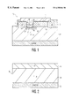
- FIG. 1 shows an LMOSFET 10 as disclosed in commonly-assigned copending U.S. patent application Ser. No. 09/469,454 entitled “Self-Aligned Silicon Carbide LMOSFET”.
- This SiC LMOSFET includes a self-aligned gate structure and offers protection against gate reach through.
- the LMOSFET 10 of FIG. 1 includes highly n-doped source and drain regions 11 , 12 , a lightly n-doped drift region 13 formed by an N- epitaxial layer 14 , and an electrically insulated self-aligned gate structure 15 comprised of a gate oxide 16 and a gate metal 17 , formed on a lightly-doped p-type SiC epitaxial layer 18 (P-epilayer).
- the gate structure 15 has edges 19 which are substantially aligned with the edges 20 of the source and drift regions 11 , 13 . Accordingly, the gate-to-source and gate-to-drift region overlap can be advantageously controlled by the thickness of the gate metal 17 , which can be selected to be very small.
- a channel region 21 in the P- epilayer 18 The channel region 21 changes from p-type to n-type due to inversion when a positive voltage greater than the threshold voltage of the LMOSFET 10 is applied to the gate 15 thereby providing a low resistance current path between the source region 11 and drift extension 13 of the drain region 12 .
- the LMOSFET 10 of FIG. 1 should provide many advantages in terms of better linearity, efficiency and power density at comparable frequencies, and higher frequency operation than Si LDMOSFETs.
- this LMOSFET may suffer from higher forward voltage drop, i.e., higher “on-resistance” due to the fact that the current at the source side has to flow around a corner 22 where the gate oxide 16 has a greater thickness.
- the greater oxide thickness results in a higher resistivity portion in inversion, which will likely result in higher forward voltage drop.
- the LMOSFET comprises a first layer of SiC semiconductor material having a p-type conductivity and a second layer of SiC semiconductor material having an n-type conductivity formed on the first layer.
- Source and drain regions having n-type conductivities are formed in the second SiC semiconductor layer.
- An etched trench extends through the second SiC semiconductor layer and partially into the first SiC semiconductor layer so that the source and drain regions are substantially lateral thereto.
- the trench is coated with a layer of an electrically insulating oxide material and partially filled with a layer of metallic material thereby forming a gate structure.
- a channel region is defined in the first layer beneath the gate structure.
- the source comer of the gate structure is either rounded or surrounded by the source region to provide a current path in the channel region which avoids sharp corners. Electrical contacts associated with the source and drain regions, and the gate structure establish source, drain, and gate electrodes.
- FIG. 1 is a cross-sectional view of a SiC LDMOSFET as disclosed in commonly assigned copending U.S. patent application Ser. No. 09/469,454 entitled “Self-Aligned Silicon Carbide LMOSFET”;
- FIG. 2 is a cross-sectional view of a starting wafer used for fabricating a SiC LMOSFET having a self-aligned gate with gate reach-through protection according to a first embodiment of the invention
- FIGS. 3-5 are cross-sectional views of the wafer of FIG. 2 depicting various steps used in fabrication of the SiC LMOSFET of the invention
- FIG. 6 is a cross-sectional view of the completed SiC LMOSFET according to the first embodiment of the invention.
- FIG. 7 is a cross-sectional view of a SiC LMOSFET having a self-aligned gate with gate reach-through protection according to a second embodiment of the invention.
- FIG. 2 shows a layered wafer 30 used for fabricating a SiC lateral metal-oxide-semiconductor field effect transistor (LMOSFET) having a self-aligned gate structure with improved gate reach-through protection according to an embodiment of the invention.
- the wafer 30 comprises a substrate 32 with a P-epitaxial layer 34 (P-epilayer) grown on top of the substrate 32 , and a lightly-doped n-type epitaxial SiC layer 36 (N-epilayer) grown on top of the P-epilayer 34 .
- the substrate 32 can be made from any suitable n or p doped Si or SiC semiconductor material, or an insulating material such as undoped Si, undoped SiC, or glass.
- the P- and N-epilayers 34 , 36 are epitaxially grown using conventional methods such as chemical vapor deposition CVD, and are doped using conventional aluminum, boron or nitrogen incorporation during epitaxial growth.
- the thickness and doping of the P-epilayer 34 are selected according to the desired electrical breakdown voltage of the LMOSFET.
- the thickness (selected to be as small as possible) and doping of the N-epilayer 36 are selected using the reduced surface field (RESURF) effect according to the desired breakdown voltage of the LMOSFET.
- the doping concentration of the N-epilayer 36 is also selected independent of that of the P-epilayer 34 .
- source and drain regions 40 , 42 are fabricated first in the layered wafer 30 by selectively implanting an N+ dopant in the top surface thereof.
- the implant depth is selected to be substantially equal to or slightly greater than (as shown) the thickness of the N-epilayer 36 .
- the N+ dopant is then activated using any desired processing temperature. Note that the N-epilayer will advantageously form a lightly n-doped extension of the drain region otherwise known as a drift region 43 .
- a trench 44 is etched through the N-epilayer 36 and partially into the P-epilayer 34 .
- the trench 44 has first and second opposing sides 46 , 48 connected by a curved bottom 50 which substantially eliminates sharp comers where the sides 46 , 48 and bottom 50 meet by rounding them out.
- Such a trench geometry can be achieved using conventional reactive ion etching (RIE) techniques and chemical compounds adapted to provide an etching directionality that produces rounding of the trench bottom 50 .
- RIE reactive ion etching
- the rounded trench bottom 50 can also be achieved using wet etching techniques which typically produce trenches with curved bottoms due to the isotropic nature of the etching.
- the etching should be performed so that the first side 46 of the trench 44 overlaps into the source region 40 and the trench 44 should have a depth which is greater than the depth of the source region 40 .
- a layer 52 of oxide material such as silicon dioxide is formed on the sides 46 , 48 and curved bottom 50 of the trench 44 using any preferred conventional method such as deposition, thermal oxidation, or combination thereof
- the curved trench geometry allows the oxide layer 52 to be formed therein with a uniform thickness.
- the trench 44 is then partially filled with a layer 54 of metallic material such as polysilicon.
- the layer 54 metallic material can be deposited in the trench 44 using any preferred conventional method such as sputtering or chemical vapor deposition (CVD).
- the layer 54 of metallic material in cooperation with the underlying layer 52 of oxide material forms a self-aligned, curved gate structure 56 with rounded corners 61 and edges 57 which are substantially aligned with the edges 59 of the source and drift regions 40 , 43 .
- the gate-to-source and gate-to-drift region (edge) overlap can be advantageously controlled by the thickness of the gate metal 54 , which can be selected to be very small.
- FIG. 6 shows the completed SiC LMOSFET 60 of the invention.
- the LMOSFET 60 is finalized by applying a second layer 62 of oxide material such as silicon dioxide over the top of the layered wafer 30 shown in FIG. 5 .
- the second layer 62 of oxide material fills the remainder of the trench 44 and electrically isolates the top of the wafer 30 .
- Windows 64 , 66 are defined in the oxide layers 62 , 52 to provide access to the source region 40 , the self-aligned gate structure 56 (window is located laterally and not visible in this view) and the drain region 42 .
- electrically conductive contacts 68 , 70 to the source region 40 , gate 56 (contact not visible) and drain region 42 are deposited in the windows 64 , 66 using conventional techniques.
- the contacts 68 , 70 (including the contact not visible in the drawings) and their corresponding source region 40 , drain region 42 , and gate structure 56 , define source, drain, and gate electrodes of the LMOSFET 60 .
- the LMOSFET 60 includes a channel region 72 defined in the P-epilayer 34 directly beneath the gate electrode structure 56 .
- the channel region 72 changes from p-type to n-type due to inversion when a positive voltage greater than the threshold voltage of the LMOSFET 60 is applied to the gate 56 .
- the gate structure 56 is curved with rounded corners 61 , carriers in the channel region 72 do not need to make any sharp turns (eliminating sharp turns advantageously makes the gate oxide thickness uniform and decreases the “on-resistance” in the channel region 72 ) during inversion.
- the channel 72 provides a gradually curving, very low resistance current path between the source region 40 and drift region 43 during inversion. This in turn, decreases forward voltage drop in the LMOSFET 60 .
- FIG. 7 shows a SiC LMOSFET 80 having a self-aligned gate with gate reach-through protection according to a second embodiment of the invention, wherein like numerals identify like elements.
- This LMOSFET 80 is substantially similar in structure and fabrication to the LMOSFET of FIG. 6 except that the gate structure 85 (comprised of a gate oxide 86 and a gate metal 87 ) is fabricated with a flat bottom trench 90 that has corners 94 , 95 where the sides 91 , 92 and bottom 93 meet. Additionally, the source and drain regions 82 , 83 have an increased implant depth D such that they now extend entirely through the N-epilayer 36 and significantly into the P-epilayer 34 .
- the increased implant depth D allows the source region 82 to extend below and enclose the source side corner 94 of the gate structure 85 (sacrificing some self-alignment on the source side, i.e., increased gate-to-source region overlap) so that the corner 94 is completely surrounded by the source region 82 .
- This provides a channel region 88 which does not have to turn a corner on the source side of the gate structure 85 thereby lowering the channel resistivity during inversion and consequently reducing forward voltage drop of the LMOSFET 80 .
- the drain side corner 95 of the gate structure 85 does not substantially contribute to increased resistivity during inversion because a depletion layer 96 extending in the P-epilayer 34 aids in sweeping the charge carriers away from the drain side corner 95 of the gate structure 85 . Therefore, the carriers move in a generally straight path as they move toward the drift region 84 , instead of turning sharply into the drift region 84 as they pass the drain side corner 95 of the gate structure 85 .
- the present LMOSFET structures advantageously provide channel regions in the P-epilayers.
- the channel region in each LMOSFET changes from p-type to n-type due to inversion when a positive voltage greater than the threshold voltage of the LMOSFET is applied to the gate thereby providing a low resistance current path between the source region and drift region.
- Additional advantages realized with the present LMOSFETs include substantial alleviation of gate reach through as the depletion does not spread laterally towards the source in these designs.
- the depletion in these structures is restricted to drift region and the P-epilayer underneath the drift region.
- Further advantages come from the drift region being formed by an N-epilayer which has superior mobility values in comparison to implanted N-layers. Consequently, the epitaxial formed drift region increases the electrical breakdown voltage of the LMOSFET without undesirably increasing the “on-resistance” thereof.
- the use of the epitaxial formed drift region also provides the designer with greater freedom in specifying the doping concentration and thickness of this region, than drift regions formed using implantation.
- the LMOSFETs of the invention also have smaller pitch sizes.
- the SiC LMOSFETs of the invention should provide better linearity, efficiency and power density at comparable frequencies, and higher frequency operation than Si LDMOSFETs. Accordingly, the SiC LMOSFETs of the invention can replace Si LDMOSFETs in UHF transmitters at 2 GHz and extend the transmission range up to at least 4 GHz.
Landscapes
- Insulated Gate Type Field-Effect Transistor (AREA)
- Electrodes Of Semiconductors (AREA)
Abstract
A silicon carbide LMOSFET having a self-aligned gate with gate reach-through protection and method for making same. The LMOSFET includes a first layer of SiC semiconductor material having a p-type conductivity and a second layer of SiC semiconductor material having an n-type conductivity formed on the first layer. Source and drain regions having n-type conductivities are formed in the second SiC semiconductor layer. An etched trench extends through the second SiC semiconductor layer and partially into the first SiC semiconductor layer. The trench is coated with a layer of an electrically insulating oxide material and partially filled with a layer of metallic material thereby forming a gate structure. A channel region is defined in the first layer beneath the gate structure. The gate structure is rounded or buried to provide a current path in the channel region which avoids sharp corners.
Description
Commonly-assigned, copending U.S. patent application Ser. No. 09/469,454, entitled “Self-Aligned Silicon Carbide LMOSFET”, filed Dec. 12, 1999.
Commonly-assigned, copending U.S. patent application Ser. No. 09/469,450, entitled “Silicon Carbide N-Channel Power LMOSFET”, FILED Dec. 12, 1999.
This invention relates to lateral metal-oxide-semiconductor field effect transistors (LMOSFETs) used in high-power applications such as UHF transmission which are especially suited for silicon carbide (SiC) technology. In particular, the invention relates to a SiC LMOSFET having a self-aligned gate structure with improved gate reach-through protection and methods of fabricating same.
In recent years, the use of silicon lateral double-diffused metal-oxide-semiconductor field effect transistors (Si LDMOSFETs) in high-power and high-frequency applications has increased enormously. This is because Si LDMOSFETs offer simpler gate drive and faster response than bipolar devices.
Si LDMOSFETs are typically fabricated using self-aligned techniques, which minimize gate overlap of the source and drift/drain regions. Minimal overlap is critical for maintaining low gate-to-source and gate-to-drift/drain capacitances, which can adversely affect the high frequency performance of the device. It is also desirable to reduce the overlap to decrease the cell pitch and conserve the silicon area used by the device.
Silicon carbide (SiC) is an attractive semiconductor material for high frequency and high power applications. The properties which make SiC attractive for high power UHF applications are its large critical electric field (10 times that of Si) and its large electron saturation velocity (2 times that of Si). The large critical electric field helps increase the breakdown voltage of the device and the large saturation velocity helps increase the peak current.
FIG. 1 shows an LMOSFET 10 as disclosed in commonly-assigned copending U.S. patent application Ser. No. 09/469,454 entitled “Self-Aligned Silicon Carbide LMOSFET”. This SiC LMOSFET includes a self-aligned gate structure and offers protection against gate reach through. The LMOSFET 10 of FIG. 1 includes highly n-doped source and drain regions 11, 12, a lightly n-doped drift region 13 formed by an N- epitaxial layer 14, and an electrically insulated self-aligned gate structure 15 comprised of a gate oxide 16 and a gate metal 17, formed on a lightly-doped p-type SiC epitaxial layer 18 (P-epilayer). The gate structure 15 has edges 19 which are substantially aligned with the edges 20 of the source and drift regions 11, 13. Accordingly, the gate-to-source and gate-to-drift region overlap can be advantageously controlled by the thickness of the gate metal 17, which can be selected to be very small. A channel region 21 in the P- epilayer 18. The channel region 21changes from p-type to n-type due to inversion when a positive voltage greater than the threshold voltage of the LMOSFET 10 is applied to the gate 15 thereby providing a low resistance current path between the source region 11 and drift extension 13 of the drain region 12.
The LMOSFET 10 of FIG. 1 should provide many advantages in terms of better linearity, efficiency and power density at comparable frequencies, and higher frequency operation than Si LDMOSFETs. However, this LMOSFET may suffer from higher forward voltage drop, i.e., higher “on-resistance” due to the fact that the current at the source side has to flow around a corner 22 where the gate oxide 16 has a greater thickness. The greater oxide thickness results in a higher resistivity portion in inversion, which will likely result in higher forward voltage drop.
Therefore, a SiC LMOSFET is needed which overcomes the above problem.
Summarily described is an LMOSFET having a self-aligned gate with gate reach-through protection and method for making same. The LMOSFET comprises a first layer of SiC semiconductor material having a p-type conductivity and a second layer of SiC semiconductor material having an n-type conductivity formed on the first layer. Source and drain regions having n-type conductivities are formed in the second SiC semiconductor layer. An etched trench extends through the second SiC semiconductor layer and partially into the first SiC semiconductor layer so that the source and drain regions are substantially lateral thereto. The trench is coated with a layer of an electrically insulating oxide material and partially filled with a layer of metallic material thereby forming a gate structure. A channel region is defined in the first layer beneath the gate structure. The source comer of the gate structure is either rounded or surrounded by the source region to provide a current path in the channel region which avoids sharp corners. Electrical contacts associated with the source and drain regions, and the gate structure establish source, drain, and gate electrodes.
The advantages, nature, and various additional features of the invention will appear more fully upon consideration of the illustrative embodiment now to be described in detail in connection with accompanying drawings wherein:
FIG. 1 is a cross-sectional view of a SiC LDMOSFET as disclosed in commonly assigned copending U.S. patent application Ser. No. 09/469,454 entitled “Self-Aligned Silicon Carbide LMOSFET”;
FIG. 2 is a cross-sectional view of a starting wafer used for fabricating a SiC LMOSFET having a self-aligned gate with gate reach-through protection according to a first embodiment of the invention;
FIGS. 3-5 are cross-sectional views of the wafer of FIG. 2 depicting various steps used in fabrication of the SiC LMOSFET of the invention;
FIG. 6 is a cross-sectional view of the completed SiC LMOSFET according to the first embodiment of the invention; and
FIG. 7 is a cross-sectional view of a SiC LMOSFET having a self-aligned gate with gate reach-through protection according to a second embodiment of the invention.
It should be understood that the drawings are for purposes of illustrating the concepts of the invention and are not to scale.
FIG. 2 shows a layered wafer 30 used for fabricating a SiC lateral metal-oxide-semiconductor field effect transistor (LMOSFET) having a self-aligned gate structure with improved gate reach-through protection according to an embodiment of the invention. The wafer 30 comprises a substrate 32 with a P-epitaxial layer 34 (P-epilayer) grown on top of the substrate 32, and a lightly-doped n-type epitaxial SiC layer 36 (N-epilayer) grown on top of the P-epilayer 34. The substrate 32 can be made from any suitable n or p doped Si or SiC semiconductor material, or an insulating material such as undoped Si, undoped SiC, or glass. The P- and N- epilayers 34, 36 are epitaxially grown using conventional methods such as chemical vapor deposition CVD, and are doped using conventional aluminum, boron or nitrogen incorporation during epitaxial growth. The thickness and doping of the P-epilayer 34 are selected according to the desired electrical breakdown voltage of the LMOSFET. The thickness (selected to be as small as possible) and doping of the N-epilayer 36 are selected using the reduced surface field (RESURF) effect according to the desired breakdown voltage of the LMOSFET. The doping concentration of the N-epilayer 36 is also selected independent of that of the P-epilayer 34.
As shown in FIG. 3, source and drain regions 40, 42 are fabricated first in the layered wafer 30 by selectively implanting an N+ dopant in the top surface thereof. The implant depth is selected to be substantially equal to or slightly greater than (as shown) the thickness of the N-epilayer 36. The N+ dopant is then activated using any desired processing temperature. Note that the N-epilayer will advantageously form a lightly n-doped extension of the drain region otherwise known as a drift region 43.
In FIG. 4, a trench 44 is etched through the N-epilayer 36 and partially into the P-epilayer 34. The trench 44 has first and second opposing sides 46, 48 connected by a curved bottom 50 which substantially eliminates sharp comers where the sides 46, 48 and bottom 50 meet by rounding them out. Such a trench geometry can be achieved using conventional reactive ion etching (RIE) techniques and chemical compounds adapted to provide an etching directionality that produces rounding of the trench bottom 50. The rounded trench bottom 50 can also be achieved using wet etching techniques which typically produce trenches with curved bottoms due to the isotropic nature of the etching. The etching should be performed so that the first side 46 of the trench 44 overlaps into the source region 40 and the trench 44 should have a depth which is greater than the depth of the source region 40.
In FIG. 5, a layer 52 of oxide material such as silicon dioxide is formed on the sides 46, 48 and curved bottom 50 of the trench 44 using any preferred conventional method such as deposition, thermal oxidation, or combination thereof The curved trench geometry allows the oxide layer 52 to be formed therein with a uniform thickness. The trench 44 is then partially filled with a layer 54 of metallic material such as polysilicon. The layer 54 metallic material can be deposited in the trench 44 using any preferred conventional method such as sputtering or chemical vapor deposition (CVD). The layer 54 of metallic material in cooperation with the underlying layer 52 of oxide material forms a self-aligned, curved gate structure 56 with rounded corners 61 and edges 57 which are substantially aligned with the edges 59 of the source and drift regions 40, 43. The gate-to-source and gate-to-drift region (edge) overlap can be advantageously controlled by the thickness of the gate metal 54, which can be selected to be very small.
FIG. 6 shows the completed SiC LMOSFET 60 of the invention. The LMOSFET 60 is finalized by applying a second layer 62 of oxide material such as silicon dioxide over the top of the layered wafer 30 shown in FIG. 5. The second layer 62 of oxide material fills the remainder of the trench 44 and electrically isolates the top of the wafer 30. Windows 64, 66 are defined in the oxide layers 62, 52 to provide access to the source region 40, the self-aligned gate structure 56 (window is located laterally and not visible in this view) and the drain region 42. Finally, electrically conductive contacts 68, 70 to the source region 40, gate 56 (contact not visible) and drain region 42, are deposited in the windows 64, 66 using conventional techniques. The contacts 68, 70 (including the contact not visible in the drawings) and their corresponding source region 40, drain region 42, and gate structure 56, define source, drain, and gate electrodes of the LMOSFET 60.
The LMOSFET 60 includes a channel region 72 defined in the P-epilayer 34 directly beneath the gate electrode structure 56. The channel region 72 changes from p-type to n-type due to inversion when a positive voltage greater than the threshold voltage of the LMOSFET 60 is applied to the gate 56. Because the gate structure 56 is curved with rounded corners 61, carriers in the channel region 72 do not need to make any sharp turns (eliminating sharp turns advantageously makes the gate oxide thickness uniform and decreases the “on-resistance” in the channel region 72) during inversion. Hence, the channel 72 provides a gradually curving, very low resistance current path between the source region 40 and drift region 43 during inversion. This in turn, decreases forward voltage drop in the LMOSFET 60.
FIG. 7 shows a SiC LMOSFET 80 having a self-aligned gate with gate reach-through protection according to a second embodiment of the invention, wherein like numerals identify like elements. This LMOSFET 80 is substantially similar in structure and fabrication to the LMOSFET of FIG. 6 except that the gate structure 85 (comprised of a gate oxide 86 and a gate metal 87) is fabricated with a flat bottom trench 90 that has corners 94, 95 where the sides 91, 92 and bottom 93 meet. Additionally, the source and drain regions 82, 83 have an increased implant depth D such that they now extend entirely through the N-epilayer 36 and significantly into the P-epilayer 34. The increased implant depth D allows the source region 82 to extend below and enclose the source side corner 94 of the gate structure 85 (sacrificing some self-alignment on the source side, i.e., increased gate-to-source region overlap) so that the corner 94 is completely surrounded by the source region 82. This provides a channel region 88 which does not have to turn a corner on the source side of the gate structure 85 thereby lowering the channel resistivity during inversion and consequently reducing forward voltage drop of the LMOSFET 80. The drain side corner 95 of the gate structure 85 does not substantially contribute to increased resistivity during inversion because a depletion layer 96 extending in the P-epilayer 34 aids in sweeping the charge carriers away from the drain side corner 95 of the gate structure 85. Therefore, the carriers move in a generally straight path as they move toward the drift region 84, instead of turning sharply into the drift region 84 as they pass the drain side corner 95 of the gate structure 85.
In addition to providing a self-aligned gate structure with minimal gate-to-source and gate-to-drift region overlap, the present LMOSFET structures advantageously provide channel regions in the P-epilayers. The channel region in each LMOSFET changes from p-type to n-type due to inversion when a positive voltage greater than the threshold voltage of the LMOSFET is applied to the gate thereby providing a low resistance current path between the source region and drift region.
Additional advantages realized with the present LMOSFETs include substantial alleviation of gate reach through as the depletion does not spread laterally towards the source in these designs. The depletion in these structures is restricted to drift region and the P-epilayer underneath the drift region. Further advantages come from the drift region being formed by an N-epilayer which has superior mobility values in comparison to implanted N-layers. Consequently, the epitaxial formed drift region increases the electrical breakdown voltage of the LMOSFET without undesirably increasing the “on-resistance” thereof. The use of the epitaxial formed drift region also provides the designer with greater freedom in specifying the doping concentration and thickness of this region, than drift regions formed using implantation. The LMOSFETs of the invention also have smaller pitch sizes.
Still further, the SiC LMOSFETs of the invention should provide better linearity, efficiency and power density at comparable frequencies, and higher frequency operation than Si LDMOSFETs. Accordingly, the SiC LMOSFETs of the invention can replace Si LDMOSFETs in UHF transmitters at 2 GHz and extend the transmission range up to at least 4 GHz.
While the foregoing invention has been described with reference to the above embodiments, various modifications and changes can be made without departing from the spirit of the invention. Accordingly, all such modifications and changes are considered to be within the scope of the appended claims.
Claims (9)
1. A lateral metal-oxide-semiconductor field effect transistor (LMOSFET) comprising:
a first layer of silicon carbide semiconductor material having a p-type conductivity;
a second layer of silicon carbide semiconductor material having an n-type conductivity formed on the first layer;
source and drain regions having n-type conductivities formed in the second silicon carbide semiconductor layer, the n-type conductivities of the source and drain regions being greater than then-type conductivity of the second silicon carbide layer;
a trench extending through the second silicon carbide semiconductor layer and partially into the first silicon carbide semiconductor layer, so that the source and drain regions are substantially lateral thereto, the drain region being spaced apart from the trench by a portion of the second layer which forms a drift region, the trench coated with a layer of an electrically insulating oxide material and partially filled with a layer of metallic material, the layers of oxide and metallic material forming a self-aligned gate structure;
a channel region defined in the first layer beneath the gate structure; and
electrical contacts associated with the source and drain regions, and the gate structure thereby establishing source, drain, and gate electrodes;
wherein the gate structure is adapted to provide a current path in the channel region which avoids sharp corners.
2. The LMOSFET according to claim 1 , further comprising a substrate which supports the first and second silicon carbide semiconductor layers.
3. The LMOSFET according to claim 1 , wherein the first layer of silicon carbide semiconductor material is an epitaxial layer.
4. The LMOSFET according to claim 1 , wherein the second layer of silicon carbide semiconductor material is an epitaxial layer.
5. The LMOSFET according to claim 4 , wherein the epitaxial second layer of silicon carbide semiconductor material defines a drift region that extends laterally from the drain region to the gate structure, the gate structure being substantially aligned with the source and drift regions.
6. The LMOSFET according to claim 1 , wherein the source and drain regions each have a depth which is at least equal to the thickness of the second layer of silicon carbide material.
7. The LMOSFET according to claim 6 , wherein the trench includes a curved bottom that provides the gate structure with rounded corners.
8. The LMOSFET according to claim 1 , wherein the source region extends partially into the first layer of silicon carbide semiconductor material and has a depth which is greater than the depth of the trench.
9. The LMOSFET according to claim 1 , wherein the source and drain regions are implanted regions.
Priority Applications (5)
| Application Number | Priority Date | Filing Date | Title |
|---|---|---|---|
| US09/469,451 US6355944B1 (en) | 1999-12-21 | 1999-12-21 | Silicon carbide LMOSFET with gate reach-through protection |
| KR1020017010588A KR20010102278A (en) | 1999-12-21 | 2000-11-20 | Silicon carbide lmosfet with gate break-down protection |
| EP00988733A EP1161771A1 (en) | 1999-12-21 | 2000-11-20 | Silicon carbide lmosfet with gate break-down protection |
| PCT/EP2000/011543 WO2001047026A1 (en) | 1999-12-21 | 2000-11-20 | Silicon carbide lmosfet with gate break-down protection |
| JP2001547662A JP2003518749A (en) | 1999-12-21 | 2000-11-20 | Silicon carbide LMOSFET with gate breakdown protection |
Applications Claiming Priority (1)
| Application Number | Priority Date | Filing Date | Title |
|---|---|---|---|
| US09/469,451 US6355944B1 (en) | 1999-12-21 | 1999-12-21 | Silicon carbide LMOSFET with gate reach-through protection |
Publications (1)
| Publication Number | Publication Date |
|---|---|
| US6355944B1 true US6355944B1 (en) | 2002-03-12 |
Family
ID=23863853
Family Applications (1)
| Application Number | Title | Priority Date | Filing Date |
|---|---|---|---|
| US09/469,451 Expired - Fee Related US6355944B1 (en) | 1999-12-21 | 1999-12-21 | Silicon carbide LMOSFET with gate reach-through protection |
Country Status (5)
| Country | Link |
|---|---|
| US (1) | US6355944B1 (en) |
| EP (1) | EP1161771A1 (en) |
| JP (1) | JP2003518749A (en) |
| KR (1) | KR20010102278A (en) |
| WO (1) | WO2001047026A1 (en) |
Cited By (8)
| Publication number | Priority date | Publication date | Assignee | Title |
|---|---|---|---|---|
| US6620697B1 (en) * | 2001-09-24 | 2003-09-16 | Koninklijke Philips Electronics N.V. | Silicon carbide lateral metal-oxide semiconductor field-effect transistor having a self-aligned drift region and method for forming the same |
| US20040036113A1 (en) * | 1998-09-01 | 2004-02-26 | Fuji Electric Co., Ltd. | Silicon carbide n channel MOS semiconductor device and method for manufacturing the same |
| US20040147078A1 (en) * | 2001-05-30 | 2004-07-29 | Fuji Electric Co., Ltd. | Semiconductor device and a method for manufacturing same |
| US20050194631A1 (en) * | 2004-03-04 | 2005-09-08 | Pinghai Hao | EEPROM with etched tunneling window |
| US20060022239A1 (en) * | 2004-07-28 | 2006-02-02 | Chandra Mouli | Memory devices, transistors, memory cells, and methods of making same |
| US9129835B2 (en) | 2012-10-08 | 2015-09-08 | Samsung Electronics Co., Ltd. | Semiconductor device and method of manufacturing the same |
| US20160181371A1 (en) * | 2013-07-19 | 2016-06-23 | Nissan Motor Co., Ltd. | Semiconductor device and method of manufacturing the same |
| CN108735798A (en) * | 2018-04-02 | 2018-11-02 | 上海芯研亮投资咨询有限公司 | SiC FET components and its manufacturing method with low starting voltage |
Families Citing this family (2)
| Publication number | Priority date | Publication date | Assignee | Title |
|---|---|---|---|---|
| US6323506B1 (en) * | 1999-12-21 | 2001-11-27 | Philips Electronics North America Corporation | Self-aligned silicon carbide LMOSFET |
| JP5344477B2 (en) * | 2009-08-28 | 2013-11-20 | 独立行政法人産業技術総合研究所 | Insulated gate silicon carbide lateral field effect transistor with recessed gate structure |
Citations (7)
| Publication number | Priority date | Publication date | Assignee | Title |
|---|---|---|---|---|
| JPS63287064A (en) | 1987-05-19 | 1988-11-24 | Fujitsu Ltd | Mis type semiconductor device and manufacture thereof |
| JPH02110973A (en) | 1988-10-19 | 1990-04-24 | Toshiba Corp | Mos type semiconductor device and manufacture thereof |
| US5726463A (en) * | 1992-08-07 | 1998-03-10 | General Electric Company | Silicon carbide MOSFET having self-aligned gate structure |
| JPH11103058A (en) * | 1997-07-31 | 1999-04-13 | Toshiba Corp | Semiconductor device |
| US5915180A (en) | 1994-04-06 | 1999-06-22 | Denso Corporation | Process for producing a semiconductor device having a single thermal oxidizing step |
| US6011278A (en) * | 1997-10-28 | 2000-01-04 | Philips Electronics North America Corporation | Lateral silicon carbide semiconductor device having a drift region with a varying doping level |
| US6198127B1 (en) * | 1999-05-19 | 2001-03-06 | Intersil Corporation | MOS-gated power device having extended trench and doping zone and process for forming same |
Family Cites Families (6)
| Publication number | Priority date | Publication date | Assignee | Title |
|---|---|---|---|---|
| JPS6070766A (en) * | 1983-09-26 | 1985-04-22 | Mitsubishi Electric Corp | Mos type semiconductor device |
| JPH0294477A (en) * | 1988-09-30 | 1990-04-05 | Toshiba Corp | Semiconductor device and manufacture thereof |
| US5399515A (en) * | 1993-07-12 | 1995-03-21 | Motorola, Inc. | Method of fabricating a silicon carbide vertical MOSFET and device |
| JPH0888283A (en) * | 1994-09-16 | 1996-04-02 | Fuji Electric Co Ltd | Silicon carbide complementary MOSFET |
| JPH08213606A (en) * | 1995-02-06 | 1996-08-20 | Fuji Electric Co Ltd | Silicon Carbide Horizontal High Voltage MOSFET |
| US6057558A (en) * | 1997-03-05 | 2000-05-02 | Denson Corporation | Silicon carbide semiconductor device and manufacturing method thereof |
-
1999
- 1999-12-21 US US09/469,451 patent/US6355944B1/en not_active Expired - Fee Related
-
2000
- 2000-11-20 EP EP00988733A patent/EP1161771A1/en not_active Withdrawn
- 2000-11-20 WO PCT/EP2000/011543 patent/WO2001047026A1/en not_active Ceased
- 2000-11-20 KR KR1020017010588A patent/KR20010102278A/en not_active Withdrawn
- 2000-11-20 JP JP2001547662A patent/JP2003518749A/en active Pending
Patent Citations (7)
| Publication number | Priority date | Publication date | Assignee | Title |
|---|---|---|---|---|
| JPS63287064A (en) | 1987-05-19 | 1988-11-24 | Fujitsu Ltd | Mis type semiconductor device and manufacture thereof |
| JPH02110973A (en) | 1988-10-19 | 1990-04-24 | Toshiba Corp | Mos type semiconductor device and manufacture thereof |
| US5726463A (en) * | 1992-08-07 | 1998-03-10 | General Electric Company | Silicon carbide MOSFET having self-aligned gate structure |
| US5915180A (en) | 1994-04-06 | 1999-06-22 | Denso Corporation | Process for producing a semiconductor device having a single thermal oxidizing step |
| JPH11103058A (en) * | 1997-07-31 | 1999-04-13 | Toshiba Corp | Semiconductor device |
| US6011278A (en) * | 1997-10-28 | 2000-01-04 | Philips Electronics North America Corporation | Lateral silicon carbide semiconductor device having a drift region with a varying doping level |
| US6198127B1 (en) * | 1999-05-19 | 2001-03-06 | Intersil Corporation | MOS-gated power device having extended trench and doping zone and process for forming same |
Non-Patent Citations (2)
| Title |
|---|
| PHA 23,899, "Self-Aligned Silicon Carbide LMOSFET", filed concurrently herewith. |
| PHA 23,900, "Silicon Carbide N-Channel Power LMOSFET", filed concurrently herewith. |
Cited By (19)
| Publication number | Priority date | Publication date | Assignee | Title |
|---|---|---|---|---|
| US20040036113A1 (en) * | 1998-09-01 | 2004-02-26 | Fuji Electric Co., Ltd. | Silicon carbide n channel MOS semiconductor device and method for manufacturing the same |
| US20040147078A1 (en) * | 2001-05-30 | 2004-07-29 | Fuji Electric Co., Ltd. | Semiconductor device and a method for manufacturing same |
| US7056793B2 (en) * | 2001-05-30 | 2006-06-06 | Fuji Electric Co., Ltd. | Semiconductor device and a method for manufacturing same |
| US6620697B1 (en) * | 2001-09-24 | 2003-09-16 | Koninklijke Philips Electronics N.V. | Silicon carbide lateral metal-oxide semiconductor field-effect transistor having a self-aligned drift region and method for forming the same |
| US7307309B2 (en) * | 2004-03-04 | 2007-12-11 | Texas Instruments Incorporated | EEPROM with etched tunneling window |
| US20050194631A1 (en) * | 2004-03-04 | 2005-09-08 | Pinghai Hao | EEPROM with etched tunneling window |
| WO2006012626A3 (en) * | 2004-07-28 | 2008-04-17 | Micron Technology Inc | Memory devices, transistors, memory cells, and methods of making same |
| US20060197137A1 (en) * | 2004-07-28 | 2006-09-07 | Chandra Mouli | Memory devices, transistors, memory cells, and methods of making same |
| US20060022239A1 (en) * | 2004-07-28 | 2006-02-02 | Chandra Mouli | Memory devices, transistors, memory cells, and methods of making same |
| US7598134B2 (en) | 2004-07-28 | 2009-10-06 | Micron Technology, Inc. | Memory device forming methods |
| US8080837B2 (en) | 2004-07-28 | 2011-12-20 | Micron Technology, Inc. | Memory devices, transistors, and memory cells |
| US8415722B2 (en) | 2004-07-28 | 2013-04-09 | Micron Technology, Inc. | Memory devices and memory cells |
| US8470666B2 (en) | 2004-07-28 | 2013-06-25 | Micron Technology, Inc. | Methods of making random access memory devices, transistors, and memory cells |
| CN101288166B (en) * | 2004-07-28 | 2013-06-26 | 美光科技公司 | Memory device, transistor, memory cell, and manufacturing method thereof |
| US8703566B2 (en) | 2004-07-28 | 2014-04-22 | Micron Technology, Inc. | Transistors comprising a SiC-containing channel |
| US9129835B2 (en) | 2012-10-08 | 2015-09-08 | Samsung Electronics Co., Ltd. | Semiconductor device and method of manufacturing the same |
| US20160181371A1 (en) * | 2013-07-19 | 2016-06-23 | Nissan Motor Co., Ltd. | Semiconductor device and method of manufacturing the same |
| US10861938B2 (en) * | 2013-07-19 | 2020-12-08 | Nissan Motor Co., Ltd. | Semiconductor device and method of manufacturing the same |
| CN108735798A (en) * | 2018-04-02 | 2018-11-02 | 上海芯研亮投资咨询有限公司 | SiC FET components and its manufacturing method with low starting voltage |
Also Published As
| Publication number | Publication date |
|---|---|
| KR20010102278A (en) | 2001-11-15 |
| WO2001047026A1 (en) | 2001-06-28 |
| JP2003518749A (en) | 2003-06-10 |
| EP1161771A1 (en) | 2001-12-12 |
Similar Documents
| Publication | Publication Date | Title |
|---|---|---|
| US7291894B2 (en) | Vertical charge control semiconductor device with low output capacitance | |
| CN112614891A (en) | Mosfet with enhanced high frequency performance | |
| CN100524809C (en) | A field effect transistor semiconductor device | |
| EP1396030B1 (en) | Vertical power semiconductor device and method of making the same | |
| US7126166B2 (en) | High voltage lateral FET structure with improved on resistance performance | |
| US5349224A (en) | Integrable MOS and IGBT devices having trench gate structure | |
| US20030060013A1 (en) | Method of manufacturing trench field effect transistors with trenched heavy body | |
| EP1170803A2 (en) | Trench gate MOSFET and method of making the same | |
| EP2362423A2 (en) | Vertical power semiconductor device and method of making the same | |
| EP1177583B1 (en) | Silicon carbide lateral mosfet and method of making the same | |
| WO1996030947A1 (en) | Punch-through field effect transistor | |
| EP1312121A2 (en) | Power mosfet and methods of forming and operating the same | |
| US20250241017A1 (en) | Vertical trench coupling capacitance gated-controlled junction field effect transistor and manufacturing method thereof | |
| CN121001361A (en) | A capacitor, power structure, and switching power supply voltage regulator circuit. | |
| US6355944B1 (en) | Silicon carbide LMOSFET with gate reach-through protection | |
| US20200194583A1 (en) | Metal source ldmos semiconductor device and manufacturing method thereof | |
| CN115188812A (en) | MOSFET with split planar gate structure | |
| US7671441B2 (en) | Trench MOSFET with sidewall spacer gates | |
| CN102449770B (en) | 3D channel architecture for semiconductor devices | |
| US6593594B1 (en) | Silicon carbide n-channel power LMOSFET | |
| US20190334019A1 (en) | Top structure of insulated gate bipolar transistor (igbt) with improved injection enhancement | |
| CN118136678B (en) | Double-gate double-channel LDMOS device and manufacturing method | |
| CN120980922A (en) | A semiconductor device | |
| CN118645530A (en) | Trench gate power semiconductor field effect transistor |
Legal Events
| Date | Code | Title | Description |
|---|---|---|---|
| AS | Assignment |
Owner name: PHILIPS ELECTRONICS NORTH AMERICA CORPORATION, NEW Free format text: ASSIGNMENT OF ASSIGNORS INTEREST;ASSIGNOR:ALOK, DEV;REEL/FRAME:010511/0283 Effective date: 19991216 |
|
| REMI | Maintenance fee reminder mailed | ||
| LAPS | Lapse for failure to pay maintenance fees | ||
| STCH | Information on status: patent discontinuation |
Free format text: PATENT EXPIRED DUE TO NONPAYMENT OF MAINTENANCE FEES UNDER 37 CFR 1.362 |
|
| FP | Lapsed due to failure to pay maintenance fee |
Effective date: 20060312 |