US20060251886A1 - Electronic devices comprising an organic conductor and semiconductor as well as an intermediate buffer layer made of a crosslinked polymer - Google Patents
Electronic devices comprising an organic conductor and semiconductor as well as an intermediate buffer layer made of a crosslinked polymer Download PDFInfo
- Publication number
- US20060251886A1 US20060251886A1 US10/570,372 US57037206A US2006251886A1 US 20060251886 A1 US20060251886 A1 US 20060251886A1 US 57037206 A US57037206 A US 57037206A US 2006251886 A1 US2006251886 A1 US 2006251886A1
- Authority
- US
- United States
- Prior art keywords
- atoms
- buffer layer
- organic
- electronic device
- organic electronic
- Prior art date
- Legal status (The legal status is an assumption and is not a legal conclusion. Google has not performed a legal analysis and makes no representation as to the accuracy of the status listed.)
- Granted
Links
- 239000004065 semiconductor Substances 0.000 title claims abstract description 38
- 239000004020 conductor Substances 0.000 title description 3
- 229920006037 cross link polymer Polymers 0.000 title description 2
- 229920000642 polymer Polymers 0.000 claims abstract description 59
- 238000004132 cross linking Methods 0.000 claims abstract description 33
- 239000000463 material Substances 0.000 claims abstract description 31
- 238000000034 method Methods 0.000 claims abstract description 31
- 238000007639 printing Methods 0.000 claims abstract description 21
- 230000008569 process Effects 0.000 claims abstract description 14
- 238000007669 thermal treatment Methods 0.000 claims abstract description 4
- 125000003118 aryl group Chemical group 0.000 claims description 25
- 125000004432 carbon atom Chemical group C* 0.000 claims description 25
- 125000004435 hydrogen atom Chemical group [H]* 0.000 claims description 24
- 125000002091 cationic group Chemical group 0.000 claims description 11
- 125000005842 heteroatom Chemical group 0.000 claims description 10
- 125000003342 alkenyl group Chemical group 0.000 claims description 9
- 125000006165 cyclic alkyl group Chemical group 0.000 claims description 9
- 229910052739 hydrogen Inorganic materials 0.000 claims description 9
- 239000001257 hydrogen Substances 0.000 claims description 9
- 125000003545 alkoxy group Chemical group 0.000 claims description 7
- 229920000767 polyaniline Polymers 0.000 claims description 7
- YTPLMLYBLZKORZ-UHFFFAOYSA-N Thiophene Chemical compound C=1C=CSC=1 YTPLMLYBLZKORZ-UHFFFAOYSA-N 0.000 claims description 6
- 125000001931 aliphatic group Chemical group 0.000 claims description 6
- 229910052736 halogen Inorganic materials 0.000 claims description 6
- 150000002367 halogens Chemical class 0.000 claims description 6
- 125000002950 monocyclic group Chemical group 0.000 claims description 6
- 125000003367 polycyclic group Chemical group 0.000 claims description 6
- 238000007151 ring opening polymerisation reaction Methods 0.000 claims description 6
- 125000005309 thioalkoxy group Chemical group 0.000 claims description 6
- 125000005259 triarylamine group Chemical group 0.000 claims description 6
- 229920000547 conjugated polymer Polymers 0.000 claims description 5
- 125000004122 cyclic group Chemical group 0.000 claims description 5
- 230000003287 optical effect Effects 0.000 claims description 5
- 229920000123 polythiophene Polymers 0.000 claims description 5
- 239000002253 acid Substances 0.000 claims description 4
- 230000005669 field effect Effects 0.000 claims description 4
- 239000010409 thin film Substances 0.000 claims description 4
- 150000007513 acids Chemical class 0.000 claims description 3
- 150000001336 alkenes Chemical class 0.000 claims description 3
- 125000004183 alkoxy alkyl group Chemical group 0.000 claims description 3
- 229920001577 copolymer Polymers 0.000 claims description 3
- JRZJOMJEPLMPRA-UHFFFAOYSA-N olefin Natural products CCCCCCCC=C JRZJOMJEPLMPRA-UHFFFAOYSA-N 0.000 claims description 3
- 229930192474 thiophene Natural products 0.000 claims description 3
- ICPSWZFVWAPUKF-UHFFFAOYSA-N 1,1'-spirobi[fluorene] Chemical class C1=CC=C2C=C3C4(C=5C(C6=CC=CC=C6C=5)=CC=C4)C=CC=C3C2=C1 ICPSWZFVWAPUKF-UHFFFAOYSA-N 0.000 claims description 2
- 125000001140 1,4-phenylene group Chemical group [H]C1=C([H])C([*:2])=C([H])C([H])=C1[*:1] 0.000 claims description 2
- RICKKZXCGCSLIU-UHFFFAOYSA-N 2-[2-[carboxymethyl-[[3-hydroxy-5-(hydroxymethyl)-2-methylpyridin-4-yl]methyl]amino]ethyl-[[3-hydroxy-5-(hydroxymethyl)-2-methylpyridin-4-yl]methyl]amino]acetic acid Chemical compound CC1=NC=C(CO)C(CN(CCN(CC(O)=O)CC=2C(=C(C)N=CC=2CO)O)CC(O)=O)=C1O RICKKZXCGCSLIU-UHFFFAOYSA-N 0.000 claims description 2
- 241000702619 Porcine parvovirus Species 0.000 claims description 2
- PJULCNAVAGQLAT-UHFFFAOYSA-N indeno[2,1-a]fluorene Chemical class C1=CC=C2C=C3C4=CC5=CC=CC=C5C4=CC=C3C2=C1 PJULCNAVAGQLAT-UHFFFAOYSA-N 0.000 claims description 2
- 239000007800 oxidant agent Substances 0.000 claims description 2
- 238000004803 parallel plate viscometry Methods 0.000 claims description 2
- 229920000553 poly(phenylenevinylene) Polymers 0.000 claims description 2
- 229920002098 polyfluorene Polymers 0.000 claims description 2
- 238000010791 quenching Methods 0.000 claims description 2
- 125000003983 fluorenyl group Chemical class C1(=CC=CC=2C3=CC=CC=C3CC12)* 0.000 claims 1
- 150000002391 heterocyclic compounds Chemical class 0.000 claims 1
- 238000007641 inkjet printing Methods 0.000 abstract description 16
- 230000009477 glass transition Effects 0.000 abstract description 8
- 230000005855 radiation Effects 0.000 abstract description 4
- 230000003381 solubilizing effect Effects 0.000 abstract 1
- 239000010410 layer Substances 0.000 description 140
- -1 hexafluoroantimonate Chemical compound 0.000 description 19
- YXFVVABEGXRONW-UHFFFAOYSA-N Toluene Chemical compound CC1=CC=CC=C1 YXFVVABEGXRONW-UHFFFAOYSA-N 0.000 description 12
- 239000002184 metal Substances 0.000 description 10
- 238000002347 injection Methods 0.000 description 9
- 239000007924 injection Substances 0.000 description 9
- 229910052751 metal Inorganic materials 0.000 description 9
- 239000000243 solution Substances 0.000 description 9
- 150000001875 compounds Chemical class 0.000 description 8
- 238000004519 manufacturing process Methods 0.000 description 8
- 238000004528 spin coating Methods 0.000 description 8
- 239000011229 interlayer Substances 0.000 description 7
- 150000002739 metals Chemical class 0.000 description 7
- 239000000203 mixture Substances 0.000 description 7
- WYURNTSHIVDZCO-UHFFFAOYSA-N Tetrahydrofuran Chemical compound C1CCOC1 WYURNTSHIVDZCO-UHFFFAOYSA-N 0.000 description 6
- 239000011368 organic material Substances 0.000 description 6
- 229910052760 oxygen Inorganic materials 0.000 description 6
- 239000011521 glass Substances 0.000 description 5
- 150000003254 radicals Chemical class 0.000 description 5
- 239000002904 solvent Substances 0.000 description 5
- 239000000758 substrate Substances 0.000 description 5
- 238000000137 annealing Methods 0.000 description 4
- 238000006243 chemical reaction Methods 0.000 description 4
- 239000002322 conducting polymer Substances 0.000 description 4
- 229920001940 conductive polymer Polymers 0.000 description 4
- 125000006413 ring segment Chemical group 0.000 description 4
- RWRDLPDLKQPQOW-UHFFFAOYSA-N Pyrrolidine Chemical compound C1CCNC1 RWRDLPDLKQPQOW-UHFFFAOYSA-N 0.000 description 3
- 230000000052 comparative effect Effects 0.000 description 3
- 238000000151 deposition Methods 0.000 description 3
- 230000008021 deposition Effects 0.000 description 3
- 238000004770 highest occupied molecular orbital Methods 0.000 description 3
- 239000012535 impurity Substances 0.000 description 3
- 229910052757 nitrogen Inorganic materials 0.000 description 3
- 239000003960 organic solvent Substances 0.000 description 3
- 150000003384 small molecules Chemical class 0.000 description 3
- 239000000126 substance Substances 0.000 description 3
- 229910052717 sulfur Inorganic materials 0.000 description 3
- RYHBNJHYFVUHQT-UHFFFAOYSA-N 1,4-Dioxane Chemical compound C1COCCO1 RYHBNJHYFVUHQT-UHFFFAOYSA-N 0.000 description 2
- 239000007848 Bronsted acid Substances 0.000 description 2
- CPLXHLVBOLITMK-UHFFFAOYSA-N Magnesium oxide Chemical compound [Mg]=O CPLXHLVBOLITMK-UHFFFAOYSA-N 0.000 description 2
- NQRYJNQNLNOLGT-UHFFFAOYSA-N Piperidine Chemical compound C1CCNCC1 NQRYJNQNLNOLGT-UHFFFAOYSA-N 0.000 description 2
- 150000001340 alkali metals Chemical class 0.000 description 2
- RDOXTESZEPMUJZ-UHFFFAOYSA-N anisole Chemical compound COC1=CC=CC=C1 RDOXTESZEPMUJZ-UHFFFAOYSA-N 0.000 description 2
- QVGXLLKOCUKJST-UHFFFAOYSA-N atomic oxygen Chemical compound [O] QVGXLLKOCUKJST-UHFFFAOYSA-N 0.000 description 2
- 229910052788 barium Inorganic materials 0.000 description 2
- 230000008901 benefit Effects 0.000 description 2
- 239000002800 charge carrier Substances 0.000 description 2
- MVPPADPHJFYWMZ-UHFFFAOYSA-N chlorobenzene Chemical compound ClC1=CC=CC=C1 MVPPADPHJFYWMZ-UHFFFAOYSA-N 0.000 description 2
- 238000000576 coating method Methods 0.000 description 2
- 239000003086 colorant Substances 0.000 description 2
- 230000021615 conjugation Effects 0.000 description 2
- 150000004292 cyclic ethers Chemical class 0.000 description 2
- 238000011161 development Methods 0.000 description 2
- 230000018109 developmental process Effects 0.000 description 2
- 238000009792 diffusion process Methods 0.000 description 2
- 238000005538 encapsulation Methods 0.000 description 2
- AMGQUBHHOARCQH-UHFFFAOYSA-N indium;oxotin Chemical compound [In].[Sn]=O AMGQUBHHOARCQH-UHFFFAOYSA-N 0.000 description 2
- 239000002346 layers by function Substances 0.000 description 2
- PQXKHYXIUOZZFA-UHFFFAOYSA-M lithium fluoride Chemical compound [Li+].[F-] PQXKHYXIUOZZFA-UHFFFAOYSA-M 0.000 description 2
- 229910044991 metal oxide Inorganic materials 0.000 description 2
- 150000004706 metal oxides Chemical class 0.000 description 2
- 150000002894 organic compounds Chemical class 0.000 description 2
- 239000012044 organic layer Substances 0.000 description 2
- 125000002524 organometallic group Chemical group 0.000 description 2
- 239000001301 oxygen Substances 0.000 description 2
- 229910052698 phosphorus Inorganic materials 0.000 description 2
- 229920000172 poly(styrenesulfonic acid) Polymers 0.000 description 2
- 229910052710 silicon Inorganic materials 0.000 description 2
- 229910052709 silver Inorganic materials 0.000 description 2
- PUZPDOWCWNUUKD-UHFFFAOYSA-M sodium fluoride Chemical compound [F-].[Na+] PUZPDOWCWNUUKD-UHFFFAOYSA-M 0.000 description 2
- 239000011877 solvent mixture Substances 0.000 description 2
- 238000009987 spinning Methods 0.000 description 2
- 125000001424 substituent group Chemical group 0.000 description 2
- 238000006467 substitution reaction Methods 0.000 description 2
- XLYOFNOQVPJJNP-UHFFFAOYSA-N water Substances O XLYOFNOQVPJJNP-UHFFFAOYSA-N 0.000 description 2
- BGJSXRVXTHVRSN-UHFFFAOYSA-N 1,3,5-trioxane Chemical compound C1OCOCO1 BGJSXRVXTHVRSN-UHFFFAOYSA-N 0.000 description 1
- CZLMRJZAHXYRIX-UHFFFAOYSA-N 1,3-dioxepane Chemical compound C1CCOCOC1 CZLMRJZAHXYRIX-UHFFFAOYSA-N 0.000 description 1
- WNXJIVFYUVYPPR-UHFFFAOYSA-N 1,3-dioxolane Chemical compound C1COCO1 WNXJIVFYUVYPPR-UHFFFAOYSA-N 0.000 description 1
- JECYNCQXXKQDJN-UHFFFAOYSA-N 2-(2-methylhexan-2-yloxymethyl)oxirane Chemical compound CCCCC(C)(C)OCC1CO1 JECYNCQXXKQDJN-UHFFFAOYSA-N 0.000 description 1
- 229920000536 2-Acrylamido-2-methylpropane sulfonic acid Polymers 0.000 description 1
- MGADZUXDNSDTHW-UHFFFAOYSA-N 2H-pyran Chemical compound C1OC=CC=C1 MGADZUXDNSDTHW-UHFFFAOYSA-N 0.000 description 1
- XYVMOLOUBJBNBF-UHFFFAOYSA-N 3h-1,3-oxazol-2-one Chemical class OC1=NC=CO1 XYVMOLOUBJBNBF-UHFFFAOYSA-N 0.000 description 1
- NOWKCMXCCJGMRR-UHFFFAOYSA-N Aziridine Chemical compound C1CN1 NOWKCMXCCJGMRR-UHFFFAOYSA-N 0.000 description 1
- 241000611421 Elia Species 0.000 description 1
- FUJCRWPEOMXPAD-UHFFFAOYSA-N Li2O Inorganic materials [Li+].[Li+].[O-2] FUJCRWPEOMXPAD-UHFFFAOYSA-N 0.000 description 1
- CBENFWSGALASAD-UHFFFAOYSA-N Ozone Chemical compound [O-][O+]=O CBENFWSGALASAD-UHFFFAOYSA-N 0.000 description 1
- 229910002842 PtOx Inorganic materials 0.000 description 1
- 229910052772 Samarium Inorganic materials 0.000 description 1
- 230000002378 acidificating effect Effects 0.000 description 1
- 229910052783 alkali metal Inorganic materials 0.000 description 1
- 229910001515 alkali metal fluoride Inorganic materials 0.000 description 1
- 229910052784 alkaline earth metal Inorganic materials 0.000 description 1
- 229910001618 alkaline earth metal fluoride Inorganic materials 0.000 description 1
- 150000001342 alkaline earth metals Chemical class 0.000 description 1
- 229910052782 aluminium Inorganic materials 0.000 description 1
- 150000001408 amides Chemical class 0.000 description 1
- 125000003277 amino group Chemical group 0.000 description 1
- 239000010405 anode material Substances 0.000 description 1
- 239000007864 aqueous solution Substances 0.000 description 1
- 125000005264 aryl amine group Chemical group 0.000 description 1
- 125000004429 atom Chemical group 0.000 description 1
- 229910001632 barium fluoride Inorganic materials 0.000 description 1
- 230000004888 barrier function Effects 0.000 description 1
- 230000015572 biosynthetic process Effects 0.000 description 1
- 230000000903 blocking effect Effects 0.000 description 1
- 229910052791 calcium Inorganic materials 0.000 description 1
- 239000000470 constituent Substances 0.000 description 1
- 238000010276 construction Methods 0.000 description 1
- 230000008878 coupling Effects 0.000 description 1
- 238000010168 coupling process Methods 0.000 description 1
- 238000005859 coupling reaction Methods 0.000 description 1
- 150000005676 cyclic carbonates Chemical group 0.000 description 1
- XUCJHNOBJLKZNU-UHFFFAOYSA-M dilithium;hydroxide Chemical compound [Li+].[Li+].[OH-] XUCJHNOBJLKZNU-UHFFFAOYSA-M 0.000 description 1
- LTYMSROWYAPPGB-UHFFFAOYSA-O diphenylsulfanium Chemical compound C=1C=CC=CC=1[SH+]C1=CC=CC=C1 LTYMSROWYAPPGB-UHFFFAOYSA-O 0.000 description 1
- 239000006185 dispersion Substances 0.000 description 1
- 238000004090 dissolution Methods 0.000 description 1
- 238000001035 drying Methods 0.000 description 1
- 239000007772 electrode material Substances 0.000 description 1
- 239000010408 film Substances 0.000 description 1
- 150000002220 fluorenes Chemical class 0.000 description 1
- 239000007789 gas Substances 0.000 description 1
- 230000008570 general process Effects 0.000 description 1
- 229910052737 gold Inorganic materials 0.000 description 1
- 238000010438 heat treatment Methods 0.000 description 1
- 125000000623 heterocyclic group Chemical group 0.000 description 1
- 230000006872 improvement Effects 0.000 description 1
- 229910052738 indium Inorganic materials 0.000 description 1
- 239000003999 initiator Substances 0.000 description 1
- 238000009413 insulation Methods 0.000 description 1
- 239000012212 insulator Substances 0.000 description 1
- 230000002452 interceptive effect Effects 0.000 description 1
- 150000002596 lactones Chemical group 0.000 description 1
- 229910052747 lanthanoid Inorganic materials 0.000 description 1
- 150000002602 lanthanoids Chemical class 0.000 description 1
- 239000007788 liquid Substances 0.000 description 1
- 229920002521 macromolecule Polymers 0.000 description 1
- 229910052749 magnesium Inorganic materials 0.000 description 1
- 229910001092 metal group alloy Inorganic materials 0.000 description 1
- UZKWTJUDCOPSNM-UHFFFAOYSA-N methoxybenzene Substances CCCCOC=C UZKWTJUDCOPSNM-UHFFFAOYSA-N 0.000 description 1
- 229910003455 mixed metal oxide Inorganic materials 0.000 description 1
- 239000000178 monomer Substances 0.000 description 1
- 125000004433 nitrogen atom Chemical group N* 0.000 description 1
- 238000007645 offset printing Methods 0.000 description 1
- 230000005693 optoelectronics Effects 0.000 description 1
- 239000013110 organic ligand Substances 0.000 description 1
- 150000002902 organometallic compounds Chemical class 0.000 description 1
- 150000002918 oxazolines Chemical class 0.000 description 1
- AHHWIHXENZJRFG-UHFFFAOYSA-N oxetane Chemical compound C1COC1 AHHWIHXENZJRFG-UHFFFAOYSA-N 0.000 description 1
- 125000003566 oxetanyl group Chemical group 0.000 description 1
- 125000004430 oxygen atom Chemical group O* 0.000 description 1
- 238000006552 photochemical reaction Methods 0.000 description 1
- 238000007750 plasma spraying Methods 0.000 description 1
- 239000004033 plastic Substances 0.000 description 1
- 229920003023 plastic Polymers 0.000 description 1
- 239000002985 plastic film Substances 0.000 description 1
- 229920006255 plastic film Polymers 0.000 description 1
- 229910052697 platinum Inorganic materials 0.000 description 1
- 229920001798 poly[2-(acrylamido)-2-methyl-1-propanesulfonic acid] polymer Polymers 0.000 description 1
- 229940005642 polystyrene sulfonic acid Drugs 0.000 description 1
- 230000001681 protective effect Effects 0.000 description 1
- 238000007363 ring formation reaction Methods 0.000 description 1
- 150000003839 salts Chemical class 0.000 description 1
- 238000004544 sputter deposition Methods 0.000 description 1
- 150000003460 sulfonic acids Chemical class 0.000 description 1
- 150000003463 sulfur Chemical class 0.000 description 1
- 125000004434 sulfur atom Chemical group 0.000 description 1
- YLQBMQCUIZJEEH-UHFFFAOYSA-N tetrahydrofuran Natural products C=1C=COC=1 YLQBMQCUIZJEEH-UHFFFAOYSA-N 0.000 description 1
- 239000008096 xylene Substances 0.000 description 1
- 150000003738 xylenes Chemical class 0.000 description 1
- YVTHLONGBIQYBO-UHFFFAOYSA-N zinc indium(3+) oxygen(2-) Chemical compound [O--].[Zn++].[In+3] YVTHLONGBIQYBO-UHFFFAOYSA-N 0.000 description 1
Classifications
-
- H—ELECTRICITY
- H10—SEMICONDUCTOR DEVICES; ELECTRIC SOLID-STATE DEVICES NOT OTHERWISE PROVIDED FOR
- H10K—ORGANIC ELECTRIC SOLID-STATE DEVICES
- H10K71/00—Manufacture or treatment specially adapted for the organic devices covered by this subclass
- H10K71/20—Changing the shape of the active layer in the devices, e.g. patterning
- H10K71/211—Changing the shape of the active layer in the devices, e.g. patterning by selective transformation of an existing layer
-
- H—ELECTRICITY
- H10—SEMICONDUCTOR DEVICES; ELECTRIC SOLID-STATE DEVICES NOT OTHERWISE PROVIDED FOR
- H10K—ORGANIC ELECTRIC SOLID-STATE DEVICES
- H10K85/00—Organic materials used in the body or electrodes of devices covered by this subclass
- H10K85/10—Organic polymers or oligomers
- H10K85/111—Organic polymers or oligomers comprising aromatic, heteroaromatic, or aryl chains, e.g. polyaniline, polyphenylene or polyphenylene vinylene
- H10K85/115—Polyfluorene; Derivatives thereof
-
- H—ELECTRICITY
- H10—SEMICONDUCTOR DEVICES; ELECTRIC SOLID-STATE DEVICES NOT OTHERWISE PROVIDED FOR
- H10K—ORGANIC ELECTRIC SOLID-STATE DEVICES
- H10K85/00—Organic materials used in the body or electrodes of devices covered by this subclass
- H10K85/10—Organic polymers or oligomers
- H10K85/151—Copolymers
-
- H—ELECTRICITY
- H10—SEMICONDUCTOR DEVICES; ELECTRIC SOLID-STATE DEVICES NOT OTHERWISE PROVIDED FOR
- H10K—ORGANIC ELECTRIC SOLID-STATE DEVICES
- H10K85/00—Organic materials used in the body or electrodes of devices covered by this subclass
- H10K85/60—Organic compounds having low molecular weight
- H10K85/631—Amine compounds having at least two aryl rest on at least one amine-nitrogen atom, e.g. triphenylamine
-
- H—ELECTRICITY
- H10—SEMICONDUCTOR DEVICES; ELECTRIC SOLID-STATE DEVICES NOT OTHERWISE PROVIDED FOR
- H10K—ORGANIC ELECTRIC SOLID-STATE DEVICES
- H10K2102/00—Constructional details relating to the organic devices covered by this subclass
- H10K2102/10—Transparent electrodes, e.g. using graphene
- H10K2102/101—Transparent electrodes, e.g. using graphene comprising transparent conductive oxides [TCO]
- H10K2102/103—Transparent electrodes, e.g. using graphene comprising transparent conductive oxides [TCO] comprising indium oxides, e.g. ITO
-
- H—ELECTRICITY
- H10—SEMICONDUCTOR DEVICES; ELECTRIC SOLID-STATE DEVICES NOT OTHERWISE PROVIDED FOR
- H10K—ORGANIC ELECTRIC SOLID-STATE DEVICES
- H10K50/00—Organic light-emitting devices
- H10K50/10—OLEDs or polymer light-emitting diodes [PLED]
- H10K50/17—Carrier injection layers
-
- H—ELECTRICITY
- H10—SEMICONDUCTOR DEVICES; ELECTRIC SOLID-STATE DEVICES NOT OTHERWISE PROVIDED FOR
- H10K—ORGANIC ELECTRIC SOLID-STATE DEVICES
- H10K85/00—Organic materials used in the body or electrodes of devices covered by this subclass
- H10K85/10—Organic polymers or oligomers
- H10K85/111—Organic polymers or oligomers comprising aromatic, heteroaromatic, or aryl chains, e.g. polyaniline, polyphenylene or polyphenylene vinylene
- H10K85/113—Heteroaromatic compounds comprising sulfur or selene, e.g. polythiophene
- H10K85/1135—Polyethylene dioxythiophene [PEDOT]; Derivatives thereof
-
- Y—GENERAL TAGGING OF NEW TECHNOLOGICAL DEVELOPMENTS; GENERAL TAGGING OF CROSS-SECTIONAL TECHNOLOGIES SPANNING OVER SEVERAL SECTIONS OF THE IPC; TECHNICAL SUBJECTS COVERED BY FORMER USPC CROSS-REFERENCE ART COLLECTIONS [XRACs] AND DIGESTS
- Y02—TECHNOLOGIES OR APPLICATIONS FOR MITIGATION OR ADAPTATION AGAINST CLIMATE CHANGE
- Y02E—REDUCTION OF GREENHOUSE GAS [GHG] EMISSIONS, RELATED TO ENERGY GENERATION, TRANSMISSION OR DISTRIBUTION
- Y02E10/00—Energy generation through renewable energy sources
- Y02E10/50—Photovoltaic [PV] energy
- Y02E10/549—Organic PV cells
-
- Y—GENERAL TAGGING OF NEW TECHNOLOGICAL DEVELOPMENTS; GENERAL TAGGING OF CROSS-SECTIONAL TECHNOLOGIES SPANNING OVER SEVERAL SECTIONS OF THE IPC; TECHNICAL SUBJECTS COVERED BY FORMER USPC CROSS-REFERENCE ART COLLECTIONS [XRACs] AND DIGESTS
- Y10—TECHNICAL SUBJECTS COVERED BY FORMER USPC
- Y10T—TECHNICAL SUBJECTS COVERED BY FORMER US CLASSIFICATION
- Y10T428/00—Stock material or miscellaneous articles
- Y10T428/26—Web or sheet containing structurally defined element or component, the element or component having a specified physical dimension
- Y10T428/263—Coating layer not in excess of 5 mils thick or equivalent
- Y10T428/264—Up to 3 mils
- Y10T428/265—1 mil or less
-
- Y—GENERAL TAGGING OF NEW TECHNOLOGICAL DEVELOPMENTS; GENERAL TAGGING OF CROSS-SECTIONAL TECHNOLOGIES SPANNING OVER SEVERAL SECTIONS OF THE IPC; TECHNICAL SUBJECTS COVERED BY FORMER USPC CROSS-REFERENCE ART COLLECTIONS [XRACs] AND DIGESTS
- Y10—TECHNICAL SUBJECTS COVERED BY FORMER USPC
- Y10T—TECHNICAL SUBJECTS COVERED BY FORMER US CLASSIFICATION
- Y10T428/00—Stock material or miscellaneous articles
- Y10T428/26—Web or sheet containing structurally defined element or component, the element or component having a specified physical dimension
- Y10T428/269—Web or sheet containing structurally defined element or component, the element or component having a specified physical dimension including synthetic resin or polymer layer or component
-
- Y—GENERAL TAGGING OF NEW TECHNOLOGICAL DEVELOPMENTS; GENERAL TAGGING OF CROSS-SECTIONAL TECHNOLOGIES SPANNING OVER SEVERAL SECTIONS OF THE IPC; TECHNICAL SUBJECTS COVERED BY FORMER USPC CROSS-REFERENCE ART COLLECTIONS [XRACs] AND DIGESTS
- Y10—TECHNICAL SUBJECTS COVERED BY FORMER USPC
- Y10T—TECHNICAL SUBJECTS COVERED BY FORMER US CLASSIFICATION
- Y10T428/00—Stock material or miscellaneous articles
- Y10T428/31504—Composite [nonstructural laminate]
- Y10T428/31511—Of epoxy ether
Definitions
- Organic-based charge-transport materials generally hole transporters based on triarylamine
- OLEDs or PLEDs organic or polymeric light-emitting diodes
- O-SCs organic solar cells
- O-FETs organic field-effect transistors
- OF-TFTs organic thin-film transistors
- O-ICs organic integrated circuits
- O-lasers organic optical amplifiers or organic laser diodes
- Electrode frequently metallic or inorganic, but also of organic or polymeric conducting materials
- One solution here consists in applying the active layer (for example the light-emitting layer in OLEDs/PLEDs; an analogous situation applies to lasers or charge-transport layers in all applications) directly in a structured manner.
- various printing techniques such as, for example, ink-jet printing (for example EP 0880303), offset printing, etc., in particular, have been considered for this purpose.
- Intensive work is currently being carried out, in particular, on the development of ink-jet printing methods, and considerable advances have recently been achieved here, so that the first commercial products produced in this way can be expected in the near future.
- an interlayer of a conducting, doped polymer is frequently introduced between the electrode (in particular the anode) and the organic semiconductor and functions as charge-injection layer ( Appl. Phys. Lett. 1997, 70, 2067-2069).
- the commonest of these polymers are polythiophene derivatives (for example poly(3,4-ethylenedioxy-2,5-thiophene), PEDOT) and polyaniline (PANI), which are generally doped with polystyrenesulfonic acid or other polymer-bound Bronsted acids and are thus brought into a conducting state.
- a material is chosen for the buffer layer whose glass-transition temperature is below that of the conducting doped polymer, and the annealing is carried out at a temperature above the glass-transition temperature of the buffer layer, but below the glass-transition temperature of the conducting doped polymer in order to avoid damaging the latter by the annealing process. In general, this causes a thin part of the buffer layer to become insoluble, generally in the order of 1 to 25 nm. For a relatively low glass-transition temperature of the buffer layer, a material having a relatively low molecular weight is required. However, such a material cannot be applied by ink-jet printing since the molecular weight should be higher for good printing properties.
- the soluble part of the buffer layer is then rinsed off by application of the organic semiconductor by spin coating, and the organic semiconductor layer is produced on the insoluble part of the buffer layer.
- a multilayered structure can be produced relatively easily here.
- application of the organic semiconductor to the buffer layer by a printing process is not possible in this way, since the solvent will then partially dissolve the soluble part of the buffer layer, and a blend of the material of the buffer layer and the organic semi-conductor will be formed. The production of structured multilayered devices is thus not possible in this way.
- EP 0637899 proposes electroluminescent arrangements having one or more layers in which at least one layer is crosslinked and which, in addition, contain at least one emitter layer and at least one charge-transport unit per layer.
- the crosslinking here can proceed by means of free radicals, anionically, cationically or via a photoinduced ring-closure reaction.
- a plurality of layers can be built up one on top of the other, and the layers can also be structured induced by radiation.
- ChemPhysChem 2000, 207 describes a triarylamine layer based on low-molecular-weight compounds which is crosslinked via oxetane groups as interlayer between a conducting doped polymer and an organic luminescent semiconductor. Relatively high efficiency was obtained here.
- a device of this type cannot be produced by printing processes, in particular ink-jet printing, since the low-molecular-weight triarylamine derivatives do not produce sufficiently viscous solutions before crosslinking.
- the electronic properties of the devices can be significantly improved if at least one crosslinkable polymeric buffer layer, preferably a cationically crosslinkable polymeric buffer layer, is introduced between the conducting doped polymer and the organic semiconductor layer.
- a crosslinkable polymeric buffer layer preferably a cationically crosslinkable polymeric buffer layer
- the crosslinking can also be initiated, for example, by irradiation with addition of a photoacid.
- a buffer layer of this type can advantageously also be applied by printing techniques, in particular ink-jet printing, since the ideal temperature for the thermal treatment here is independent of the glass-transition temperature of the material.
- the subsequent layer (the organic semiconductor layer) can also be applied by various printing techniques, in particular ink-jet printing, since there is then no risk of partial dissolution of the buffer layer and blend formation.
- the invention therefore relates to organic electronic devices comprising cathode, anode, at least one layer of a conducting, doped polymer and at least one layer of an organic semiconductor, characterised in that at least one conducting or semiconducting, preferably semiconducting, crosslinkable polymeric buffer layer, preferably a cationically crosslinkable buffer layer, is introduced between these two layers.
- the semiconducting polymeric buffer layer is, for the crosslinking, preferably admixed with less than 3% by weight of a photoacid, particularly preferably less than 1 % by weight, very particularly preferably with no photoacid.
- a photoacid is a compound which liberates a protic acid through a photochemical reaction on irradiation with actinic radiation.
- photoacids are 4-(thiophenoxyphenyl)diphenylsulfonium hexafluoroantimonate, (4-[(2-hydroxy-tetradecyl)oxyl]phenyl ⁇ phenyliodonium hexafluoroantimonate and others, as described, for example, in EP 1308781.
- the photoacid can be added for the crosslinking reaction, preferably with a proportion of about 0.5 to 3% by weight being selected, but does not necessarily have to be added.
- electronic devices are organic or polymeric light-emitting diodes (OLEDs, PLEDs, for example EP 0 676 461, WO 98/27136), organic solar cells (O-SCs, for example WO 98/48433, WO 94/05045), organic field-effect transistors (O-FETs, for example U.S. Pat. No. 5,705,826, U.S. Pat. No.
- organic means that at least one layer of an organic conducting doped polymer, at least one conducting or semiconducting polymeric buffer layer and at least one layer comprising at least one organic semiconductor are present; it is also possible for further organic layers (for example electrodes, etc.) to be present. However, it is also possible for layers which are not based on organic materials, such as, for example, further interlayers or electrodes, to be present.
- the electronic device is constructed from substrate (usually glass or plastic film), electrode, interlayer of a conducting, doped polymer, crosslinkable buffer layer according to the invention, organic semi-conductor and counterelectrode.
- substrate usually glass or plastic film
- electrode interlayer of a conducting, doped polymer
- crosslinkable buffer layer according to the invention
- organic semi-conductor and counterelectrode organic semi-conductor and counterelectrode.
- This device is correspondingly (depending on the application) structured, provided with contacts and finally hermetically sealed since the service life of devices of this type is drastically shortened in the presence of water and/or air.
- a conducting, doped polymer as electrode material for one or both electrodes and not to introduce an interlayer of conducting, doped polymer.
- the structure also contains a further electrode (gate), which is separated from the organic semiconductor by an insulator layer having a generally high (or more rarely low) dielectric constant.
- a further electrode which is separated from the organic semiconductor by an insulator layer having a generally high (or more rarely low) dielectric constant.
- the electrodes are selected so that their potential corresponds as well as possible to the potential of the adjacent organic layer in order to ensure the most efficient electron or hole injection possible.
- the cathode is preferably metals having a low work function, metal alloys or multilayered structures of various metals, such as, for example, alkaline-earth metals, alkali metals, main-group metals or lanthanoids (for example Ca, Ba, Mg, Al, In, Mg, Yb, Sm, etc.).
- metals which have a relatively high work function, such as, for example, Ag, may also be used in addition to the said metals, in which case combinations of the metals, such as, for example, Ca/Ag or Ba/Ag, are generally used.
- a thin interlayer of a material having a high dielectric constant between a metallic cathode and the organic semiconductor may also be preferred.
- Suitable for this purpose are, for example, alkali metal or alkaline-earth metal fluorides, but also the corresponding oxides (for example LiF, Li 2 O, BaF 2 , MgO, NaF, etc.).
- the layer thickness of this dielectric layer is preferably between 1 and 10 nm.
- the anode is preferably materials having a high work function.
- the anode preferably has a potential of greater than 4.5 eV vs. vacuum. Suitable for this purpose are on the one hand metals having a high redox potential, such as, for example, Ag, Pt or Au.
- Metal/metal oxide electrodes for example Al/Ni/NiOX, Al/Pt/PtOx may also be preferred.
- At least one of the electrodes must be transparent in order to facilitate either irradiation of the organic material (O-SC) or the coupling out of light (OLED/PLED, O-LASER).
- O-SC organic material
- O-LASER the coupling out of light
- a preferred construction uses a trans-parent anode.
- Preferred anode materials here are conducting mixed metal oxides. Particular preference is given to indium-tin oxide (ITO) or indium-zinc oxide (IZO). Preference is furthermore given to conducting, doped organic materials, in particular conducting doped polymers.
- Suitable as charge-injection layer on the anode are various doped, conducting polymers. Preference is given to polymers which have a conductivity of >10 ⁇ 8 S/cm, depending on the application.
- the potential of the layer is preferably 4 to 6 eV vs. vacuum.
- the layer thickness is preferably between 10 and 500 nm, particularly preferably between 20 and 250 nm. Particular preference is given to the use of derivatives of polythiophene (in particular poly(3,4-ethylenedioxy-2,5-thiophene), PEDOT) and polyaniline (PANI).
- the doping is generally carried out by means of acids or oxidants.
- the doping is preferably carried out by means of polymer-bound Bronsted acids.
- polymer-bound sulfonic acids in particular poly(styrenesulfonic acid), poly(vinylsulfonic acid) and PAMPSA (poly-(2-acrylamido-2-methylpropanesulfonic acid)).
- the conducting polymer is generally applied from an aqueous solution or dispersion and is insoluble in organic solvents. This enables the subsequent layer to be applied without problems from organic solvents.
- the organic semiconductor preferably comprises at least one polymeric compound.
- This can be a single polymeric compound or a blend of two or more polymeric compounds or a blend of one or more polymeric compounds with one or more low-molecular-weight organic compounds.
- the organic semiconductor layer can preferably be applied by various printing processes, in particular by ink-jet printing processes.
- an organic material is taken to mean not only purely organic compounds, but also organometallic compounds and metal coordination compounds with organic ligands. In the case of luminescent compounds, these can either fluoresce or phosphoresce, i.e. emit light from the singlet or triplet state.
- the polymeric materials here may be conjugated, partially conjugated or non-conjugated. Preference is given to conjugated materials.
- conjugated polymers are polymers which contain in the main chain principally sp 2 -hybridised carbon atoms, which may also be replaced by corresponding hetero atoms.
- conjugated is likewise used in this application text if, for example, arylamine units and/or certain heterocycles (i.e. conjugation via N, O or S atoms) and/or organometallic complexes (i.e. conjugation via the metal atom) are present in the main chain.
- Typical representatives of conjugated polymers as can be used, for example, in PLEDs or O-SCs are poly-para-phenylenevinylenes (PPVs), polyfluorenes, polyspirobifluorenes, polydihydro-phenanthrenes, polyindenofluorenes, systems based in the broadest sense on poly-p-phenylenes (PPPs), and derivatives of these structures.
- PPPs poly-para-phenylenevinylenes
- PPPs poly-para-phenylenevinylenes
- PPPs poly-p-phenylenes
- materials having high charge-carrier mobility are, for example, oligo- or poly(triarylamines), oligo- or poly(thiophenes) and copolymers containing a high proportion of these units.
- the layer thickness of the organic semiconductor is preferably 10-500 nm, particularly preferably 20-250 nm, depending on the application.
- a polymeric buffer layer is therefore introduced between the conducting, doped polymer and the organic semiconductor which carries crosslinkable units, in particular cationically crosslinkable units, so that it can accommodate low-molecular-weight, cationic species and intrinsic cationic charge carriers which are able to diffuse out of the conducting, doped polymer.
- crosslinkable groups for example groups which are crosslinkable anionically or by means of free radicals, are also possible and in accordance with the invention.
- This layer furthermore serves for improved hole injection and as electron blocking layer.
- the molecular weight of the polymers used for the buffer layer before crosslinking is preferably in the range from 50 to 500 kg/mol, particularly preferably in the range from 200 to 250 g/mol. This molecular-weight range has proven particularly suitable for application by ink-jet printing. For other printing techniques, however, other molecular-weight ranges may also be preferred.
- the layer thickness of the buffer layer is preferably in the range from 1 to 300 nm, particularly preferably in the range from 15 to 200 nm, very particularly preferably in the range from 40 to 100 nm.
- the potential of the buffer layer is preferably between the potential of the conducting, doped polymer and that of the organic semiconductor in order to improve the charge injection.
- Preferred materials for the buffer layer are derived from hole-conducting materials.
- Particularly preferably suitable for this purpose are cationically crosslinkable materials based on triarylamine, based on thiophene, based on triarylphosphine or combinations of these systems, where copolymers thereof with other structures, for example fluorenes, spirobifluorenes, dihydrophenanthrenes, indenofluorenes, etc., are also suitable materials if an adequately high proportion of the above-mentioned hole-conducting units is used.
- the proportion of hole-conducting units in the polymer is particularly preferably at least 10 mol %. The potentials of these compounds can be adjusted through suitable substitution.
- a cationically crosslinkable buffer layer is able to accommodate diffusing cationic species, in particular protons, through the crosslinking reaction being initiated thereby; on the other hand, the crosslinking simultaneously makes the buffer layer insoluble, so that subsequent application of the organic semiconductor from the usual organic solvents presents no problems.
- the crosslinked buffer layer represents a further barrier against diffusion.
- Preferred polymerisable groups are therefore cationically crosslinkable groups, in particular:
- Electron-rich olefin derivatives and compounds containing heteronuclear multiple bonds with hetero atoms or hetero groups are preferably those as described in H.-G. Elias, Makromoleküle [Macromolecules], Volume 1. Fundamentals: Structure—Synthesis—Properties , Wilsonhig & Wepf Verlag, Basle, 5th Edition, 1990, pp. 392-404, without wishing thereby to restrict the variety of possible compounds.
- a general review of cationic ring-opening polymerisation is given, for example, by E. J. Goethals et al., “Cationic Ring Opening Polymerisation” ( New Methods Polym. Synth. 1992, 67-109).
- Generally suitable for this purpose are non-aromatic cyclic systems in which one or more ring atoms are, identically or differently, O, S, N, P, Si, etc.
- cyclic amines for example aziridine, azeticine, tetrahydropyrrole, piperidine
- cyclic ethers for example oxirane, oxetane, tetrahydrofuran, pyran, dioxane
- sulfur derivatives for example 1,3-dioxolane, 1,3-dioxepan, trioxane
- lactones for example 1,3-dioxolane, 1,3-dioxepan, trioxane
- lactones for example 1,3-dioxolane, 1,3-dioxepan, trioxane
- lactones for example 1,3-dioxolane, 1,3-dioxepan, trioxane
- lactones for example 1,3-dioxolane, 1,3-dioxepan, trioxane
- lactones for example 1,3-dioxolane, 1,3-dioxepan,
- R 1 is on each occurrence, identically or differently, hydrogen, a straight-chain, branched or cyclic alkyl, alkoxy or thioalkoxy group having 1 to 20 C atoms, an aromatic or heteroaromatic ring system having 4 to 24 aromatic ring atoms or an alkenyl group having 2 to 10 C atoms, in which one or more hydrogen atoms may be replaced by halogen, such as Cl and F, or CN, and one or more non-adjacent C atoms may be replaced by —O—, —S—, —CO—, —COO— or —O—CO—; a plurality of radicals R 1 here may also form a mono- or polycyclic, aliphatic or aromatic ring system with one another or with R 2 , R 3 and/or R 4 ;
- R 2 is on each occurrence, identically or differently, hydrogen, a straight-chain, branched or cyclic alkyl group having 1 to 20 C atoms, an aromatic or heteroaromatic ring system having 4 to 24 aromatic ring atoms or an alkenyl group having 2 to 10 C atoms, in which one or more hydrogen atoms may be replaced by halogen, such as Cl and F, or CN, and one or more non-adjacent C atoms may be replaced by —O—, —S—, —CO—, —COO— or —O—CO—; a plurality of radicals R 2 here may also form a mono- or polycyclic, aliphatic or aromatic ring system with one another or with R 1 , R 3 and/or R 4 ;
- X is on each occurrence, identically or differently, —O—, —S—, —CO—, —COO—, —O—CO— or a divalent group —(CR 3 R 4 ) n —;
- Z is on each occurrence, identically or differently, a divalent group —(CR 3 R 4 ) n —;
- R 3 , R 4 is on each occurrence, identically or differently, hydrogen, a straight-chain, branched or cyclic alkyl, alkoxy, alkoxyalkyl or thioalkoxy group having 1 to 20 C atoms, an aromatic or heteroaromatic ring system having 4 to 24 aromatic ring atoms or an alkenyl group having 2 to 10 C atoms, in which one or more hydrogen atoms may also be replaced by halogen, such as Cl or F, or CN; two or more radicals R 3 or R 4 here may also form a ring system with one another or also with R 1 or R 2 ;
- n is on each occurrence, identically or differently, an integer between 0 and 20, preferably between 1 and 10, in particular between 1 and 6; with the proviso that the number of these groups of the formula (I) or formula (II) or formula (III) is limited by the maximum number of available, i.e. substitutable, H atoms.
- the crosslinking of these units can be carried out, for example, by thermal treatment of the device at this stage.
- a photoacid for the crosslinking can optionally also be added. Preference is given to thermal crosslinking without addition of a photoacid.
- Further auxiliary substances may likewise optionally be added, such as, for example, salts or acids, which are added both to the buffer layer and also to the conducting polymer layer.
- This crosslinking is preferably carried out at a temperature of 80 to 200° C. and for a duration of 0.1 to 60 minutes in an inert atmosphere.
- This crosslinking is particularly preferably carried out at a temperature of 100 to 180° C. and for a duration of 1 to 30 minutes in an inert atmosphere.
- the invention furthermore relates to the use of crosslinkable polymers for the production of a buffer layer according to the invention described above.
- this crosslinkable buffer layer that is introduced between the conducting, doped polymer and the organic semiconductor offers the following advantages:
- Cationic crosslinking of the buffer layer overcomes the reliance on a low glass-transition temperature and thus on a low-molecular-weight material for the annealing.
- high-molecular-weight materials can now also be used for this purpose enables the buffer layer to be applied by ink-jet printing.
- a layer of crosslinkable buffer layer A (polymer having structure A) with a thickness of 60 nm was applied by spin coating to a device having the following layer structure: glass//150 nm ITO//H80 nm PEDOT (annealed at 200° C. for 10 min.). The device was subsequently heated at 180° C. for 1 h.
- PEDOT is a polythiophene derivative (Baytron P4083 from H. C. Starck, Goslar). The device was washed with toluene by spinning, and the resultant layer thickness was measured. A layer thickness of 60 nm ( ⁇ 2 nm) was determined for the buffer layer.
- a layer of uncrosslinkable buffer layer B (polymer having structure B) with a thickness of 60 nm was applied by spin coating to a device having the following layer structure: glass//150 nm ITO//80 nm PEDOT (annealed at 200° C. for 10 min.). The device was subsequently heated at 180° C. for 1 h. The device was washed with toluene by spinning, and the resultant layer thickness was measured. A layer thickness of 10 nm ( ⁇ 1 nm) was determined for the buffer layer.
- 80 nm of the blue-emitting polymer C were applied by spin coating to the device having a 60 nm buffer layer B (not rinsed with toluene).
- the total layer thickness measured was 170 nm ( ⁇ 3 nm).
- 80 nm of the blue-emitting polymer C were applied by spin coating to a device consisting of glass/150 nm ITO//80 nm PEDOT (annealed at 200° C. for 10 min.).
- the total layer thickness measured was 160 nm ( ⁇ 3 nm).
- Polymers A, B and C and the corresponding monomers were synthesised as described in WO 02/10129, WO 03/020790 and WO 03/048225.
- the compositions and structures of polymers A, B and C are shown below for reasons of clarity:
- the crosslinkable buffer layer enables the production of thicker, insoluble layers, to which the light-emitting polymer can then be applied.
- polymer C it is also possible to apply polymer C to crosslinked polymer A by printing techniques since the latter is no longer dissolved by solvents, while it is not possible to apply polymer C to uncrosslinked polymer B since the latter is dissolved thereby.
- Example 3 and Comparative Example 4 it is likewise evident from Example 3 and Comparative Example 4 that polymer C exhibits higher efficiency and a longer service life if it is used with a buffer layer, in contrast to Comparative Example 5, in which it was applied directly to PEDOT without a buffer layer. It is striking here that the use of a crosslinkable buffer layer leads to significantly better results (higher efficiency, longer service life) than the use of the uncrosslinkable buffer layer.
Landscapes
- Engineering & Computer Science (AREA)
- Chemical & Material Sciences (AREA)
- Materials Engineering (AREA)
- Manufacturing & Machinery (AREA)
- Physics & Mathematics (AREA)
- Spectroscopy & Molecular Physics (AREA)
- Electroluminescent Light Sources (AREA)
- Thin Film Transistor (AREA)
- Formation Of Insulating Films (AREA)
- Junction Field-Effect Transistors (AREA)
Abstract
Description
- Electronic devices which comprise organic, organometallic and/or polymeric semiconductors are being used ever more frequently in commercial products or are just about to be introduced onto the market. Examples which may be mentioned here are organic-based charge-transport materials (generally hole transporters based on triarylamine) in photocopiers and organic or polymeric light-emitting diodes (OLEDs or PLEDs) in display devices. Organic solar cells (O-SCs), organic field-effect transistors (O-FETs), organic thin-film transistors (O-TFTs), organic integrated circuits (O-ICs), organic optical amplifiers or organic laser diodes (O-lasers) are well advanced at a research stage and could achieve major importance in the future.
- Many of these devices, irrespective of the application, have the following general layer structure, which is matched correspondingly for the individual applications:
- (1) Substrate
- (2) Electrode, frequently metallic or inorganic, but also of organic or polymeric conducting materials
- (3) Charge-injection layer or interlayer for levelling of electrode unevenness (“planarisation layer”), frequently of a conducting, doped polymer
- (4) Organic semiconductor
- (5) Optionally insulation layer
- (6) Second electrode, materials as mentioned under (2)
- (7) Circuitry
- (8) Encapsulation.
- An advantage possessed by many of these organic devices, especially those based on polymeric semiconductors, is that they can be produced from solution, which is associated with less technical complexity and expenditure of resources than vacuum processes, as are generally carried out for low-molecular-weight compounds. For full-colour displays, the three basic colours (red, green, blue) have to be applied alongside one another at high resolution in individual pixels. An analogous situation applies to electronic circuits with different switching elements. Whereas, in the case of low-molecular-weight molecules that can be vapour-deposited, the individual pixels can be generated by the vapour deposition of the individual colours through shadow masks, this is not possible for polymeric materials and materials processed from solution. One solution here consists in applying the active layer (for example the light-emitting layer in OLEDs/PLEDs; an analogous situation applies to lasers or charge-transport layers in all applications) directly in a structured manner. Recently, various printing techniques, such as, for example, ink-jet printing (for example EP 0880303), offset printing, etc., in particular, have been considered for this purpose. Intensive work is currently being carried out, in particular, on the development of ink-jet printing methods, and considerable advances have recently been achieved here, so that the first commercial products produced in this way can be expected in the near future.
- In devices for organic electronics, an interlayer of a conducting, doped polymer is frequently introduced between the electrode (in particular the anode) and the organic semiconductor and functions as charge-injection layer (Appl. Phys. Lett. 1997, 70, 2067-2069). The commonest of these polymers are polythiophene derivatives (for example poly(3,4-ethylenedioxy-2,5-thiophene), PEDOT) and polyaniline (PANI), which are generally doped with polystyrenesulfonic acid or other polymer-bound Bronsted acids and are thus brought into a conducting state. Without wishing to be tied to the correctness of this specific theory in the following invention, we assume that, on operation of the device, protons or other impurities diffuse out of the acidic groups into the functional layer, where they are suspected of significantly interfering with the functionality of the device. Thus, it is assumed that these impurities reduce the efficiency and also the service life of the devices.
- More recent results (M. Leadbeater, N. Patel, B. Tierney, S. O'Connor, I. Grizzi, C. Towns, Book of Abstracts, SID Seattle, 2004) show that the introduction of a hole-conducting buffer layer between the charge-injection layer of a conducting doped polymer and the organic semiconductor results in significantly improved device properties, in particular in a significantly increased service life. In practice, the general procedure to date has been to apply this buffer layer by a surface-coating method and subsequently to anneal it. Ideally, a material is chosen for the buffer layer whose glass-transition temperature is below that of the conducting doped polymer, and the annealing is carried out at a temperature above the glass-transition temperature of the buffer layer, but below the glass-transition temperature of the conducting doped polymer in order to avoid damaging the latter by the annealing process. In general, this causes a thin part of the buffer layer to become insoluble, generally in the order of 1 to 25 nm. For a relatively low glass-transition temperature of the buffer layer, a material having a relatively low molecular weight is required. However, such a material cannot be applied by ink-jet printing since the molecular weight should be higher for good printing properties.
- The soluble part of the buffer layer is then rinsed off by application of the organic semiconductor by spin coating, and the organic semiconductor layer is produced on the insoluble part of the buffer layer. Thus, a multilayered structure can be produced relatively easily here. However, application of the organic semiconductor to the buffer layer by a printing process is not possible in this way, since the solvent will then partially dissolve the soluble part of the buffer layer, and a blend of the material of the buffer layer and the organic semi-conductor will be formed. The production of structured multilayered devices is thus not possible in this way.
- The production of a device with buffer layer exclusively by ink-jet printing is thus hitherto still not possible, since on the one hand the buffer layer cannot be applied by printing techniques owing to the low molecular weight and since on the other hand the solution of the organic semiconductor partially dissolves the buffer layer on application by printing techniques. However, since printing techniques, in particular ink-jet printing, are regarded as a very important method for the production of structured devices, but on the other hand the use of buffer layers also has considerable potential for further developments, there is thus still a clear need for improvement here.
- EP 0637899 proposes electroluminescent arrangements having one or more layers in which at least one layer is crosslinked and which, in addition, contain at least one emitter layer and at least one charge-transport unit per layer. The crosslinking here can proceed by means of free radicals, anionically, cationically or via a photoinduced ring-closure reaction. Thus, a plurality of layers can be built up one on top of the other, and the layers can also be structured induced by radiation. However, there is no teaching regarding which of the manifold crosslinking reactions can produce a suitable device and how the crosslinking reaction is best carried out. It is merely mentioned that free-radical-crosslinkable units or photocycloaddition-capable groups are preferred, that auxiliary substances of various types, such as, for example, initiators, may be present, and that the film is preferably crosslinked by means of actinic radiation. Neither are suitable device configurations described. It is thus not clear how many layers the device preferably has, how thick these should be, which classes of material are preferably involved and which thereof are to be crosslinked. It is therefore likewise incomprehensible to the person skilled in the art how the invention described can successfully be implemented in practice.
- ChemPhysChem 2000, 207, describes a triarylamine layer based on low-molecular-weight compounds which is crosslinked via oxetane groups as interlayer between a conducting doped polymer and an organic luminescent semiconductor. Relatively high efficiency was obtained here. A device of this type cannot be produced by printing processes, in particular ink-jet printing, since the low-molecular-weight triarylamine derivatives do not produce sufficiently viscous solutions before crosslinking.
- Surprisingly, it has now been found that the electronic properties of the devices can be significantly improved if at least one crosslinkable polymeric buffer layer, preferably a cationically crosslinkable polymeric buffer layer, is introduced between the conducting doped polymer and the organic semiconductor layer. Particularly good properties are obtained in the case of a buffer layer whose crosslinking is thermally induced, i.e. by increasing the temperature to 50-250° C. However, the crosslinking can also be initiated, for example, by irradiation with addition of a photoacid. In addition, a buffer layer of this type can advantageously also be applied by printing techniques, in particular ink-jet printing, since the ideal temperature for the thermal treatment here is independent of the glass-transition temperature of the material. This means that it is not necessary to rely on materials of low molecular weight, which in turn facilitates application of the layer by printing techniques. Since the buffer layer becomes insoluble due to the crosslinking, the subsequent layer (the organic semiconductor layer) can also be applied by various printing techniques, in particular ink-jet printing, since there is then no risk of partial dissolution of the buffer layer and blend formation.
- The invention therefore relates to organic electronic devices comprising cathode, anode, at least one layer of a conducting, doped polymer and at least one layer of an organic semiconductor, characterised in that at least one conducting or semiconducting, preferably semiconducting, crosslinkable polymeric buffer layer, preferably a cationically crosslinkable buffer layer, is introduced between these two layers.
- The semiconducting polymeric buffer layer is, for the crosslinking, preferably admixed with less than 3% by weight of a photoacid, particularly preferably less than 1 % by weight, very particularly preferably with no photoacid.
- Preference is furthermore given to a polymeric crosslinkable buffer layer whose crosslinking in the corresponding device arrangement can be induced thermally, i.e. by increasing the temperature without addition of further auxiliary substances, such as, for example, photoacids.
- A photoacid is a compound which liberates a protic acid through a photochemical reaction on irradiation with actinic radiation. Examples of photoacids are 4-(thiophenoxyphenyl)diphenylsulfonium hexafluoroantimonate, (4-[(2-hydroxy-tetradecyl)oxyl]phenyl}phenyliodonium hexafluoroantimonate and others, as described, for example, in EP 1308781. The photoacid can be added for the crosslinking reaction, preferably with a proportion of about 0.5 to 3% by weight being selected, but does not necessarily have to be added.
- For the purposes of this invention, electronic devices are organic or polymeric light-emitting diodes (OLEDs, PLEDs, for example EP 0 676 461, WO 98/27136), organic solar cells (O-SCs, for example WO 98/48433, WO 94/05045), organic field-effect transistors (O-FETs, for example U.S. Pat. No. 5,705,826, U.S. Pat. No. 5,596,208, WO 00/42668), organic thin-film transistors (O-TFTs), organic integrated circuits (O -ICs, for example WO 95/31833, WO 99/10939), organic field-quench elements (FQDs, for example US 2004/017148), organic optical amplifiers or organic laser diodes (O-lasers, for example WO 98/03566). For the purposes of this invention, organic means that at least one layer of an organic conducting doped polymer, at least one conducting or semiconducting polymeric buffer layer and at least one layer comprising at least one organic semiconductor are present; it is also possible for further organic layers (for example electrodes, etc.) to be present. However, it is also possible for layers which are not based on organic materials, such as, for example, further interlayers or electrodes, to be present.
- In the simplest case, the electronic device is constructed from substrate (usually glass or plastic film), electrode, interlayer of a conducting, doped polymer, crosslinkable buffer layer according to the invention, organic semi-conductor and counterelectrode. This device is correspondingly (depending on the application) structured, provided with contacts and finally hermetically sealed since the service life of devices of this type is drastically shortened in the presence of water and/or air. It may also be preferred here to use a conducting, doped polymer as electrode material for one or both electrodes and not to introduce an interlayer of conducting, doped polymer. For applications in O-FETs and O-TFTs, it is also necessary that, in addition to electrode and counterelectrode (source and drain), the structure also contains a further electrode (gate), which is separated from the organic semiconductor by an insulator layer having a generally high (or more rarely low) dielectric constant. In addition, it may be appropriate to introduce further layers into the device. The electrodes are selected so that their potential corresponds as well as possible to the potential of the adjacent organic layer in order to ensure the most efficient electron or hole injection possible. The cathode is preferably metals having a low work function, metal alloys or multilayered structures of various metals, such as, for example, alkaline-earth metals, alkali metals, main-group metals or lanthanoids (for example Ca, Ba, Mg, Al, In, Mg, Yb, Sm, etc.). In the case of multilayered structures, further metals which have a relatively high work function, such as, for example, Ag, may also be used in addition to the said metals, in which case combinations of the metals, such as, for example, Ca/Ag or Ba/Ag, are generally used.
- It may also be preferred to introduce a thin interlayer of a material having a high dielectric constant between a metallic cathode and the organic semiconductor. Suitable for this purpose are, for example, alkali metal or alkaline-earth metal fluorides, but also the corresponding oxides (for example LiF, Li2O, BaF2, MgO, NaF, etc.). The layer thickness of this dielectric layer is preferably between 1 and 10 nm.
- The anode is preferably materials having a high work function. The anode preferably has a potential of greater than 4.5 eV vs. vacuum. Suitable for this purpose are on the one hand metals having a high redox potential, such as, for example, Ag, Pt or Au. Metal/metal oxide electrodes (for example Al/Ni/NiOX, Al/Pt/PtOx) may also be preferred.
- For some applications, at least one of the electrodes must be transparent in order to facilitate either irradiation of the organic material (O-SC) or the coupling out of light (OLED/PLED, O-LASER). A preferred construction uses a trans-parent anode. Preferred anode materials here are conducting mixed metal oxides. Particular preference is given to indium-tin oxide (ITO) or indium-zinc oxide (IZO). Preference is furthermore given to conducting, doped organic materials, in particular conducting doped polymers.
- Suitable as charge-injection layer on the anode are various doped, conducting polymers. Preference is given to polymers which have a conductivity of >10−8 S/cm, depending on the application. The potential of the layer is preferably 4 to 6 eV vs. vacuum. The layer thickness is preferably between 10 and 500 nm, particularly preferably between 20 and 250 nm. Particular preference is given to the use of derivatives of polythiophene (in particular poly(3,4-ethylenedioxy-2,5-thiophene), PEDOT) and polyaniline (PANI). The doping is generally carried out by means of acids or oxidants. The doping is preferably carried out by means of polymer-bound Bronsted acids. For this purpose, particular preference is given to polymer-bound sulfonic acids, in particular poly(styrenesulfonic acid), poly(vinylsulfonic acid) and PAMPSA (poly-(2-acrylamido-2-methylpropanesulfonic acid)). The conducting polymer is generally applied from an aqueous solution or dispersion and is insoluble in organic solvents. This enables the subsequent layer to be applied without problems from organic solvents.
- The organic semiconductor preferably comprises at least one polymeric compound. This can be a single polymeric compound or a blend of two or more polymeric compounds or a blend of one or more polymeric compounds with one or more low-molecular-weight organic compounds. The organic semiconductor layer can preferably be applied by various printing processes, in particular by ink-jet printing processes. For the purposes of this invention, an organic material is taken to mean not only purely organic compounds, but also organometallic compounds and metal coordination compounds with organic ligands. In the case of luminescent compounds, these can either fluoresce or phosphoresce, i.e. emit light from the singlet or triplet state. The polymeric materials here may be conjugated, partially conjugated or non-conjugated. Preference is given to conjugated materials. For the purposes of this invention, conjugated polymers are polymers which contain in the main chain principally sp2-hybridised carbon atoms, which may also be replaced by corresponding hetero atoms. Furthermore, the term conjugated is likewise used in this application text if, for example, arylamine units and/or certain heterocycles (i.e. conjugation via N, O or S atoms) and/or organometallic complexes (i.e. conjugation via the metal atom) are present in the main chain. Typical representatives of conjugated polymers as can be used, for example, in PLEDs or O-SCs are poly-para-phenylenevinylenes (PPVs), polyfluorenes, polyspirobifluorenes, polydihydro-phenanthrenes, polyindenofluorenes, systems based in the broadest sense on poly-p-phenylenes (PPPs), and derivatives of these structures. Of particular interest for use in O-FETs are materials having high charge-carrier mobility. These are, for example, oligo- or poly(triarylamines), oligo- or poly(thiophenes) and copolymers containing a high proportion of these units. The layer thickness of the organic semiconductor is preferably 10-500 nm, particularly preferably 20-250 nm, depending on the application.
- Without wishing to be tied to a certain theory, we assume that the protons or other cationic impurities present in the conducting doped polymer are problematic and diffusion thereof out of the doped polymer is suspected of being the limiting factor for the service life of the electronic device. In addition, hole injection from the doped polymers into the organic semiconductor is often unsatisfactory.
- A polymeric buffer layer is therefore introduced between the conducting, doped polymer and the organic semiconductor which carries crosslinkable units, in particular cationically crosslinkable units, so that it can accommodate low-molecular-weight, cationic species and intrinsic cationic charge carriers which are able to diffuse out of the conducting, doped polymer. However, other crosslinkable groups, for example groups which are crosslinkable anionically or by means of free radicals, are also possible and in accordance with the invention. This layer furthermore serves for improved hole injection and as electron blocking layer. For the buffer layer, preference is given to the use of conjugated crosslinkable polymers. The molecular weight of the polymers used for the buffer layer before crosslinking is preferably in the range from 50 to 500 kg/mol, particularly preferably in the range from 200 to 250 g/mol. This molecular-weight range has proven particularly suitable for application by ink-jet printing. For other printing techniques, however, other molecular-weight ranges may also be preferred. The layer thickness of the buffer layer is preferably in the range from 1 to 300 nm, particularly preferably in the range from 15 to 200 nm, very particularly preferably in the range from 40 to 100 nm. The potential of the buffer layer is preferably between the potential of the conducting, doped polymer and that of the organic semiconductor in order to improve the charge injection. This can be achieved through a suitable choice of the materials for the buffer layer and suitable substitution of the materials. It may also be preferred to admix further crosslinkable low-molecular-weight compounds with the polymeric material of the buffer layer. This may be appropriate in order, for example, to reduce the glass-transition temperature of the mixture and thus to facilitate crosslinking at a lower temperature.
- Preferred materials for the buffer layer are derived from hole-conducting materials. Particularly preferably suitable for this purpose are cationically crosslinkable materials based on triarylamine, based on thiophene, based on triarylphosphine or combinations of these systems, where copolymers thereof with other structures, for example fluorenes, spirobifluorenes, dihydrophenanthrenes, indenofluorenes, etc., are also suitable materials if an adequately high proportion of the above-mentioned hole-conducting units is used. The proportion of hole-conducting units in the polymer is particularly preferably at least 10 mol %. The potentials of these compounds can be adjusted through suitable substitution. Thus, compounds having a lower HOMO (=highest occupied molecular orbital) are obtained through the introduction of electron-withdrawing substituents (for example F, Cl, CN, etc.), while a higher HOMO is achieved by electron-donating substituents (for example alkoxy groups, amino groups, etc.).
- Without wishing to be tied to a certain theory, we assume that a cationically crosslinkable buffer layer is able to accommodate diffusing cationic species, in particular protons, through the crosslinking reaction being initiated thereby; on the other hand, the crosslinking simultaneously makes the buffer layer insoluble, so that subsequent application of the organic semiconductor from the usual organic solvents presents no problems. The crosslinked buffer layer represents a further barrier against diffusion. Preferred polymerisable groups are therefore cationically crosslinkable groups, in particular:
- 1) electron-rich olefin derivatives,
- 2) heteronuclear multiple bonds with hetero atoms or hetero groups and
- 3) rings containing hetero atoms (for example O, S, N, P, Si, etc.) which react by cationic ring-opening polymerisation.
- Electron-rich olefin derivatives and compounds containing heteronuclear multiple bonds with hetero atoms or hetero groups are preferably those as described in H.-G. Elias, Makromoleküle [Macromolecules], Volume 1. Fundamentals: Structure—Synthesis—Properties, Hüthig & Wepf Verlag, Basle, 5th Edition, 1990, pp. 392-404, without wishing thereby to restrict the variety of possible compounds.
- Preference is given to organic materials in which at least one H atom has been replaced by a group which reacts by cationic ring-opening polymerisation. A general review of cationic ring-opening polymerisation is given, for example, by E. J. Goethals et al., “Cationic Ring Opening Polymerisation” (New Methods Polym. Synth. 1992, 67-109). Generally suitable for this purpose are non-aromatic cyclic systems in which one or more ring atoms are, identically or differently, O, S, N, P, Si, etc. Preference is given here to cyclic systems having 3 to 7 ring atoms in which 1 to 3 ring atoms are, identically or differently, O, S or N. Examples of such systems are unsubstituted or substituted cyclic amines (for example aziridine, azeticine, tetrahydropyrrole, piperidine), cyclic ethers (for example oxirane, oxetane, tetrahydrofuran, pyran, dioxane), and also the corresponding sulfur derivatives, cyclic acetals (for example 1,3-dioxolane, 1,3-dioxepan, trioxane), lactones, cyclic carbonates, but also cyclic structures which contain different heteroatoms in the ring (for example oxazolines, dihydrooxazines, oxazolones). Preference is furthermore given to cyclic siloxanes having 4 to 8 ring atoms.
- Very particular preference is given to polymeric organic materials in which at least one H atom has been replaced by a group of the formula (I), formula (II) or formula (III)

where: - R1 is on each occurrence, identically or differently, hydrogen, a straight-chain, branched or cyclic alkyl, alkoxy or thioalkoxy group having 1 to 20 C atoms, an aromatic or heteroaromatic ring system having 4 to 24 aromatic ring atoms or an alkenyl group having 2 to 10 C atoms, in which one or more hydrogen atoms may be replaced by halogen, such as Cl and F, or CN, and one or more non-adjacent C atoms may be replaced by —O—, —S—, —CO—, —COO— or —O—CO—; a plurality of radicals R1 here may also form a mono- or polycyclic, aliphatic or aromatic ring system with one another or with R2, R3 and/or R4;
- R2 is on each occurrence, identically or differently, hydrogen, a straight-chain, branched or cyclic alkyl group having 1 to 20 C atoms, an aromatic or heteroaromatic ring system having 4 to 24 aromatic ring atoms or an alkenyl group having 2 to 10 C atoms, in which one or more hydrogen atoms may be replaced by halogen, such as Cl and F, or CN, and one or more non-adjacent C atoms may be replaced by —O—, —S—, —CO—, —COO— or —O—CO—; a plurality of radicals R2 here may also form a mono- or polycyclic, aliphatic or aromatic ring system with one another or with R1, R3and/or R4;
- X is on each occurrence, identically or differently, —O—, —S—, —CO—, —COO—, —O—CO— or a divalent group —(CR3R4)n—;
- Z is on each occurrence, identically or differently, a divalent group —(CR3R4 )n—;
- R3, R4 is on each occurrence, identically or differently, hydrogen, a straight-chain, branched or cyclic alkyl, alkoxy, alkoxyalkyl or thioalkoxy group having 1 to 20 C atoms, an aromatic or heteroaromatic ring system having 4 to 24 aromatic ring atoms or an alkenyl group having 2 to 10 C atoms, in which one or more hydrogen atoms may also be replaced by halogen, such as Cl or F, or CN; two or more radicals R3 or R4 here may also form a ring system with one another or also with R1 or R2;
- n is on each occurrence, identically or differently, an integer between 0 and 20, preferably between 1 and 10, in particular between 1 and 6; with the proviso that the number of these groups of the formula (I) or formula (II) or formula (III) is limited by the maximum number of available, i.e. substitutable, H atoms.
- The crosslinking of these units can be carried out, for example, by thermal treatment of the device at this stage. A photoacid for the crosslinking can optionally also be added. Preference is given to thermal crosslinking without addition of a photoacid. Further auxiliary substances may likewise optionally be added, such as, for example, salts or acids, which are added both to the buffer layer and also to the conducting polymer layer. This crosslinking is preferably carried out at a temperature of 80 to 200° C. and for a duration of 0.1 to 60 minutes in an inert atmosphere. This crosslinking is particularly preferably carried out at a temperature of 100 to 180° C. and for a duration of 1 to 30 minutes in an inert atmosphere.
- The invention furthermore relates to the use of crosslinkable polymers for the production of a buffer layer according to the invention described above.
- For the production of the devices, the following general process, which should be adapted correspondingly to the individual case without further inventive step, is generally used:
-
- A substrate (for example glass or also a plastic) is coated with the anode (for example indium-tin oxide, ITO, etc.). The anode is subsequently structured (for example photolithographically) and connected in accordance with the desired application. The anode-coated, pre-cleaned substrate is treated with ozone or with oxygen plasma or irradiated briefly with an excimer lamp.
- A conducting polymer, for example a doped polythiophene (PEDOT) or polyaniline derivative (PANI), is subsequently applied in a thin layer to the ITO substrate by spin coating or other coating methods.
- The crosslinkable buffer layer according to the invention is applied to this layer. To this end, the corresponding compound is firstly dissolved in a solvent or solvent mixture, preferably under a protective gas, and filtered. Suitable solvents are aromatic liquids (for example toluene, xylenes, anisole, chlorobenzene), cyclic ethers (for example dioxane, methyidioxane, THF) or amides (for example NMP, DMF), but also solvent mixtures as described in WO 02/072714. The supports described above can be coated over the entire surface with these solutions, for example by spin-coating methods, or in a structured manner by printing processes, in particular ink-jet printing. The crosslinking can then be carried out (in the case of the use of cationically crosslinkable groups) by heating the device in an inert atmosphere at this stage. A photoacid can also be added and the crosslinking initiated by irradiation, also enabling structuring to be achieved. Depending on the type of crosslinkable group, the crosslinking can be initiated in various ways. Rinsing with a solvent, for example THF, can optionally subsequently be carried out. Finally, drying is carried out.
- A solution of an organic semiconductor is applied thereto. Suitable for the production of structured devices here are, in particular, printing processes, for example ink-jet printing. The crosslinking of the buffer layer makes application of the organic semiconductor from solution possible without problems without the buffer layer being dissolved in the process.
- Further functional layers, such as, for example, charge-injection or -transport layers or hole-blocking layers, can optionally be applied to these polymer layers, for example from solution, but also by vapour deposition.
- A cathode is subsequently applied. This is carried out in accordance with the prior art by a vacuum process and can take place, for example, either by thermal vapour deposition or by plasma spraying (sputtering).
- Since many of the applications react sensitively to water, oxygen or other constituents of the atmosphere, effective encapsulation of the device is vital.
- The structure described above is adapted and optimised correspondingly for the individual applications without further inventive step and can be used in general for various applications, such as organic and polymeric light-emitting diodes, organic solar cells, organic field-effect transistors, organic thin-film transistors, organic integrated circuits, organic optical amplifiers or organic laser diodes.
- Surprisingly, this crosslinkable buffer layer that is introduced between the conducting, doped polymer and the organic semiconductor offers the following advantages:
- 1) Introduction of the crosslinkable buffer layer according to the invention improves the opto-electronic properties of the electronic device compared with a device comprising no buffer layer of this type. Thus, higher efficiency and a longer service life are observed.
- 2) Crosslinking of the buffer layer enables thicker buffer layers to be produced than is possible with uncrosslinked buffer layers, which only form a thin insoluble layer by annealing and rinsing. With these thicker, crosslinked buffer layers, better device results are obtained than with uncrosslinked, thinner buffer layers in accordance with the prior art.
- 3) Cationic crosslinking of the buffer layer overcomes the reliance on a low glass-transition temperature and thus on a low-molecular-weight material for the annealing. The fact that high-molecular-weight materials can now also be used for this purpose enables the buffer layer to be applied by ink-jet printing.
- 4) Crosslinking of the buffer layer gives an insoluble layer. This enables the subsequent layer of the organic semiconductor to be applied by a printing process, for example ink-jet printing, without the buffer layer being dissolved and a blend of the material of the buffer layer and the organic semiconductor forming. This is not possible with buffer layers in accordance with the prior art and is of major importance for the production of structured devices.
- The present invention is explained in greater detail by the following examples, without wishing to be restricted thereto. In these examples, only organic and polymeric light-emitting diodes are discussed. However, the person skilled in the art will be able to produce further electronic devices, such as, for example, O-SCs, O-FETs, O-TFTs, O-ICs, organic optical amplifiers and O-lasers, to mention but a few further applications, from the examples listed without inventive step.
- A layer of crosslinkable buffer layer A (polymer having structure A) with a thickness of 60 nm was applied by spin coating to a device having the following layer structure: glass//150 nm ITO//H80 nm PEDOT (annealed at 200° C. for 10 min.). The device was subsequently heated at 180° C. for 1 h. PEDOT is a polythiophene derivative (Baytron P4083 from H. C. Starck, Goslar). The device was washed with toluene by spinning, and the resultant layer thickness was measured. A layer thickness of 60 nm (±2 nm) was determined for the buffer layer.
- A layer of uncrosslinkable buffer layer B (polymer having structure B) with a thickness of 60 nm was applied by spin coating to a device having the following layer structure: glass//150 nm ITO//80 nm PEDOT (annealed at 200° C. for 10 min.). The device was subsequently heated at 180° C. for 1 h. The device was washed with toluene by spinning, and the resultant layer thickness was measured. A layer thickness of 10 nm (±1 nm) was determined for the buffer layer.
- 80 nm of the blue-emitting polymer C were applied by spin-coating to the device having a 60 nm buffer layer A. The total layer thickness measured (PEDOT+buffer layer+emitting polymer) was 220 nm (±4 nm). The cathode used was in all cases Ba from Aldrich and Ag from Aldrich. The way in which PLEDs can be produced in general is described in detail, for example, in WO 04/037887 and the literature cited therein.
- A maximum efficiency of 4.1 cd/A and a service life of 640 h (beginning from 800 cd/m2) were measured for the device.
- 80 nm of the blue-emitting polymer C were applied by spin coating to the device having a 60 nm buffer layer B (not rinsed with toluene). The total layer thickness measured (PEDOT+buffer layer+emitting polymer) was 170 nm (±3 nm).
- A maximum efficiency of 3.5 cd/A and a service life of 420 h (beginning from 800 cd/m2) were measured for the device.
- 80 nm of the blue-emitting polymer C were applied by spin coating to a device consisting of glass/150 nm ITO//80 nm PEDOT (annealed at 200° C. for 10 min.). The total layer thickness measured (PEDOT+buffer layer+emitting polymer) was 160 nm (±3 nm).
- A maximum efficiency of 3.1 cd/A and a service life of 180 h (beginning from 800 cd/M2) were measured for the device.
- Polymers A, B and C and the corresponding monomers were synthesised as described in WO 02/10129, WO 03/020790 and WO 03/048225. The compositions and structures of polymers A, B and C are shown below for reasons of clarity:
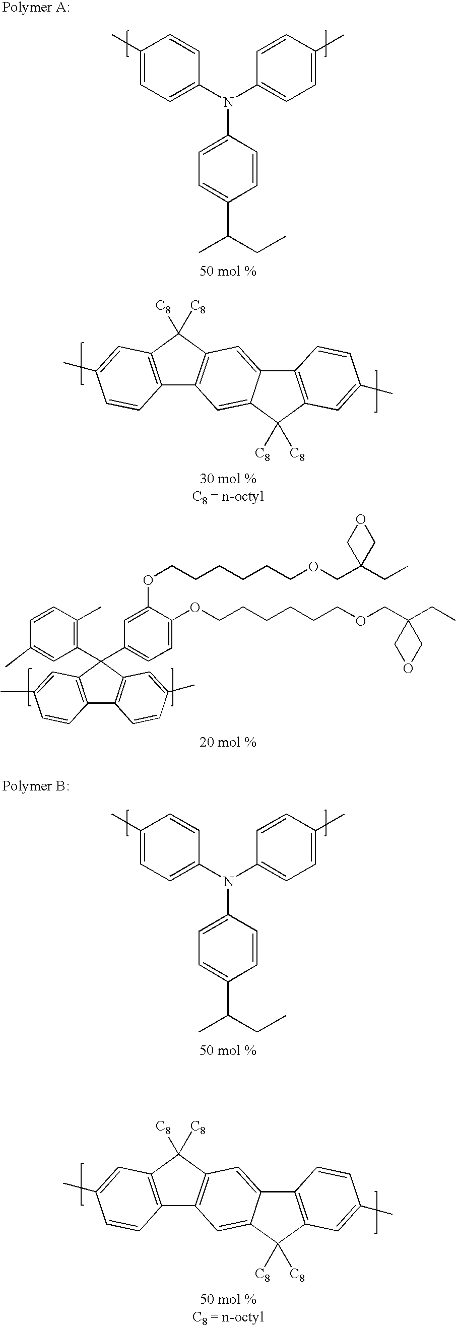

- As is thus evident from Example 1 and Comparative Example 2, the crosslinkable buffer layer enables the production of thicker, insoluble layers, to which the light-emitting polymer can then be applied. In particular, it is also possible to apply polymer C to crosslinked polymer A by printing techniques since the latter is no longer dissolved by solvents, while it is not possible to apply polymer C to uncrosslinked polymer B since the latter is dissolved thereby.
- It is likewise evident from Example 3 and Comparative Example 4 that polymer C exhibits higher efficiency and a longer service life if it is used with a buffer layer, in contrast to Comparative Example 5, in which it was applied directly to PEDOT without a buffer layer. It is striking here that the use of a crosslinkable buffer layer leads to significantly better results (higher efficiency, longer service life) than the use of the uncrosslinkable buffer layer.
Claims (23)
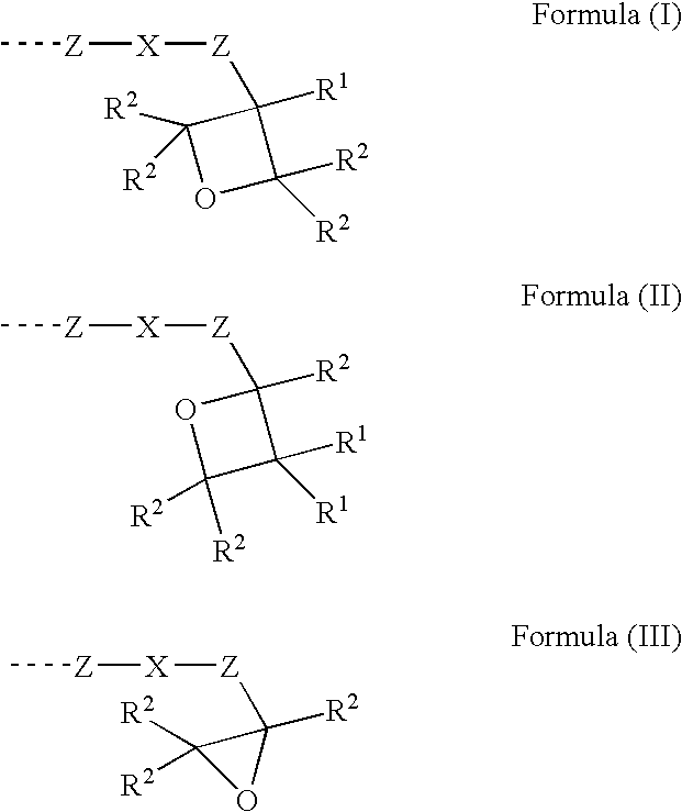
Applications Claiming Priority (4)
| Application Number | Priority Date | Filing Date | Title |
|---|---|---|---|
| DE103-40-711.1 | 2003-09-04 | ||
| DE2003140711 DE10340711A1 (en) | 2003-09-04 | 2003-09-04 | Electronic device containing organic semiconductors |
| DE10340711 | 2003-09-04 | ||
| PCT/EP2004/009903 WO2005024971A1 (en) | 2003-09-04 | 2004-09-04 | Electronic devices comprising an organic conductor and semiconductor as well as an intermediate buffer layer made of a crosslinked polymer |
Publications (2)
| Publication Number | Publication Date |
|---|---|
| US20060251886A1 true US20060251886A1 (en) | 2006-11-09 |
| US7901766B2 US7901766B2 (en) | 2011-03-08 |
Family
ID=34258390
Family Applications (2)
| Application Number | Title | Priority Date | Filing Date |
|---|---|---|---|
| US10/570,640 Abandoned US20070034862A1 (en) | 2003-09-04 | 2004-09-04 | Electronic device comprising an organic semiconductor, an organic semiconductor, and an intermediate buffer layer made of a polymer that is cationically polymerizable and contains no photoacid |
| US10/570,372 Expired - Fee Related US7901766B2 (en) | 2003-09-04 | 2004-09-04 | Electronic devices comprising an organic conductor and semiconductor as well as an intermediate buffer layer made of a crosslinked polymer |
Family Applications Before (1)
| Application Number | Title | Priority Date | Filing Date |
|---|---|---|---|
| US10/570,640 Abandoned US20070034862A1 (en) | 2003-09-04 | 2004-09-04 | Electronic device comprising an organic semiconductor, an organic semiconductor, and an intermediate buffer layer made of a polymer that is cationically polymerizable and contains no photoacid |
Country Status (8)
| Country | Link |
|---|---|
| US (2) | US20070034862A1 (en) |
| EP (2) | EP1661191B1 (en) |
| JP (3) | JP5355857B2 (en) |
| KR (2) | KR101042863B1 (en) |
| CN (2) | CN100508237C (en) |
| AT (2) | ATE492913T1 (en) |
| DE (3) | DE10340711A1 (en) |
| WO (2) | WO2005024971A1 (en) |
Cited By (13)
| Publication number | Priority date | Publication date | Assignee | Title |
|---|---|---|---|---|
| US20070034862A1 (en) * | 2003-09-04 | 2007-02-15 | Covion Organic Semiconductors Gmbh | Electronic device comprising an organic semiconductor, an organic semiconductor, and an intermediate buffer layer made of a polymer that is cationically polymerizable and contains no photoacid |
| US20070221914A1 (en) * | 2004-05-03 | 2007-09-27 | Merck Patent Gmbh Patents & Scientific Information | Electronic Devices Comprising Organic Semiconductors |
| US20090026448A1 (en) * | 2006-02-13 | 2009-01-29 | Merck Patent Gmbh | Electronic component, method for its production and its use |
| US20090149627A1 (en) * | 2006-05-12 | 2009-06-11 | Junyou Pan | Indenofluorene polymer based organic semiconductor materials |
| US20090236979A1 (en) * | 2008-03-24 | 2009-09-24 | Air Products And Chemicals, Inc. | Organic Electroluminescent Device and the Method of Making |
| US20090242842A1 (en) * | 2005-07-29 | 2009-10-01 | Kwang Suck Suh | Conducting Polymer Synthesized with Partially Substituted Polymers as a Dopant |
| US8138075B1 (en) | 2006-02-06 | 2012-03-20 | Eberlein Dietmar C | Systems and methods for the manufacture of flat panel devices |
| US8642999B2 (en) | 2007-09-18 | 2014-02-04 | Canon Kabushiki Kaisha | Organic light-emitting device and display apparatus |
| EP2112702B1 (en) * | 2007-02-15 | 2014-06-18 | Mitsubishi Chemical Corporation | Organic electroluminescent device and its method for manufacturing |
| CN104604332A (en) * | 2012-09-04 | 2015-05-06 | 三菱化学株式会社 | Organic electroluminescence element and its manufacturing method |
| US9478765B2 (en) | 2012-09-18 | 2016-10-25 | Nederlandse Organisatie Voor Toegepast-Natuurwetenschappelijk Onderzoek Tno | Electro-optical device stack, having patches covering layer breaches |
| US9502657B2 (en) | 2012-09-07 | 2016-11-22 | Pioneer Corporation | Organic electroluminescence device and manufacturing method thereof |
| US12048236B2 (en) | 2018-10-12 | 2024-07-23 | Corning Incorporated | UV patternable polymer blends for organic thin-film transistors |
Families Citing this family (36)
| Publication number | Priority date | Publication date | Assignee | Title |
|---|---|---|---|---|
| KR100738219B1 (en) * | 2003-12-23 | 2007-07-12 | 삼성에스디아이 주식회사 | Interlayer forming material for organic electroluminescent device and organic electroluminescent device using same |
| GB2425654B (en) * | 2005-04-29 | 2010-03-17 | Seiko Epson Corp | A method of fabricating a heterojunction of organic semiconducting polymers |
| US7576356B2 (en) * | 2005-08-08 | 2009-08-18 | Osram Opto Semiconductors Gmbh | Solution processed crosslinkable hole injection and hole transport polymers for OLEDs |
| US8440324B2 (en) * | 2005-12-27 | 2013-05-14 | E I Du Pont De Nemours And Company | Compositions comprising novel copolymers and electronic devices made with such compositions |
| EP2412699A1 (en) * | 2005-12-28 | 2012-02-01 | E.I. Du Pont De Nemours And Company | Compositions comprising novel compounds and electronic devices made with such compositions |
| JP4175397B2 (en) * | 2006-06-28 | 2008-11-05 | セイコーエプソン株式会社 | Method for manufacturing organic electroluminescent device |
| KR101164369B1 (en) | 2006-07-19 | 2012-07-09 | 히다치 가세고교 가부시끼가이샤 | Organic electronic material, organic electronic device and organic electroluminescent device |
| KR101532458B1 (en) * | 2007-11-21 | 2015-06-29 | 메르크 파텐트 게엠베하 | Conjugated copolymer |
| JP5540600B2 (en) * | 2008-08-13 | 2014-07-02 | 三菱化学株式会社 | Electronic device, organic electroluminescent element, organic EL display device, and organic EL lighting |
| US8643000B2 (en) * | 2008-11-18 | 2014-02-04 | E I Du Pont De Nemours And Company | Organic electronic device with low-reflectance electrode |
| JP5359255B2 (en) * | 2008-12-19 | 2013-12-04 | コニカミノルタ株式会社 | Organic photoelectric conversion element |
| JP5141600B2 (en) * | 2009-03-09 | 2013-02-13 | 三菱化学株式会社 | Method for producing composition for organic electroluminescent device |
| JP5696662B2 (en) * | 2009-06-01 | 2015-04-08 | 日立化成株式会社 | ORGANIC ELECTROLUMINESCENT ELEMENT, DISPLAY ELEMENT, LIGHTING DEVICE, AND DISPLAY DEVICE |
| ES2974909T3 (en) * | 2010-01-19 | 2024-07-02 | Sirigen Ii Ltd | New reagents for targeted amplification of a biomarker signal |
| US8859171B2 (en) * | 2010-03-03 | 2014-10-14 | Xerox Corporation | Charge transport particles |
| KR101181228B1 (en) * | 2010-10-11 | 2012-09-10 | 포항공과대학교 산학협력단 | Organic solar cell and method for preparing the same |
| KR101756657B1 (en) * | 2010-11-03 | 2017-07-12 | 엘지디스플레이 주식회사 | White organic light emitting device and display device using the same |
| JP5944120B2 (en) * | 2011-07-21 | 2016-07-05 | コニカミノルタ株式会社 | ORGANIC PHOTOELECTRIC CONVERSION DEVICE, ITS MANUFACTURING METHOD, AND ORGANIC SOLAR CELL USING THE SAME |
| DE112013004753A5 (en) * | 2012-09-27 | 2015-08-27 | Merck Patent Gmbh | Materials for organic electroluminescent devices |
| CN104838513B (en) * | 2012-12-13 | 2018-03-13 | E.I.内穆尔杜邦公司 | For preparing the method and material and the equipment that is made from it of included layer |
| KR102372211B1 (en) * | 2014-03-27 | 2022-03-08 | 닛산 가가쿠 가부시키가이샤 | Charge-transporting varnish |
| WO2015156235A1 (en) * | 2014-04-09 | 2015-10-15 | 住友化学株式会社 | Light-emission element, and composition used therein |
| JP6593432B2 (en) * | 2015-02-25 | 2019-10-23 | 三菱ケミカル株式会社 | Polymer, composition for organic electroluminescence device, organic electroluminescence device, organic EL display device and organic EL lighting |
| KR20180071277A (en) * | 2015-10-16 | 2018-06-27 | 다우 글로벌 테크놀로지스 엘엘씨 | Method for producing an organic charge transport film |
| US9644112B1 (en) * | 2016-04-20 | 2017-05-09 | Eastman Kodak Company | Articles having electrically-conductive layer or pattern |
| KR102472751B1 (en) | 2016-12-06 | 2022-11-30 | 메르크 파텐트 게엠베하 | Manufacturing method of electronic device |
| KR102476004B1 (en) * | 2017-03-24 | 2022-12-09 | 닛산 가가쿠 가부시키가이샤 | Fluorine atom-containing polymer and use thereof |
| JP2018203889A (en) | 2017-06-06 | 2018-12-27 | 日立化成株式会社 | Curable polymer, polymerization liquid, conductive film and organic light-emitting element |
| WO2019009327A1 (en) * | 2017-07-04 | 2019-01-10 | 日立化成株式会社 | Organic electronics material and organic electronics element |
| KR102385225B1 (en) | 2017-07-12 | 2022-04-11 | 삼성디스플레이 주식회사 | Composition for fabricating organic film, display device using the same and method for manufacturing the display device |
| CN107799571B (en) * | 2017-10-12 | 2020-10-09 | 武汉华星光电半导体显示技术有限公司 | Organic Light Emitting Diode Device and Display Device |
| EP3821477A1 (en) * | 2018-07-11 | 2021-05-19 | Merck Patent GmbH | Formulation containing a highly branched polymer, highly branched polymer and electro-optical device containing this highly branched polymer |
| CN118496480A (en) | 2018-11-05 | 2024-08-16 | 康宁股份有限公司 | UV patternable polymer blend for organic thin film transistor |
| KR102806396B1 (en) | 2018-12-05 | 2025-05-14 | 삼성디스플레이 주식회사 | Condensed ring compound, composition including the same and organic light-emitting device including thin film formed therefrom |
| KR20220036393A (en) | 2020-09-14 | 2022-03-23 | 삼성디스플레이 주식회사 | Display device |
| KR20220060630A (en) | 2020-11-04 | 2022-05-12 | 삼성디스플레이 주식회사 | Conductive bonding structure for boards and display device including the same |
Citations (19)
| Publication number | Priority date | Publication date | Assignee | Title |
|---|---|---|---|---|
| US4720432A (en) * | 1987-02-11 | 1988-01-19 | Eastman Kodak Company | Electroluminescent device with organic luminescent medium |
| US5518824A (en) * | 1993-08-02 | 1996-05-21 | Basf Aktiengesellschaft | Electroluminescent arrangement |
| US5596208A (en) * | 1994-12-09 | 1997-01-21 | Lucent Technologies Inc. | Article comprising an organic thin film transistor |
| US5705826A (en) * | 1994-06-28 | 1998-01-06 | Hitachi, Ltd. | Field-effect transistor having a semiconductor layer made of an organic compound |
| US5792557A (en) * | 1994-02-08 | 1998-08-11 | Tdk Corporation | Organic EL element |
| US5840217A (en) * | 1994-04-07 | 1998-11-24 | Hoechst Aktiengesellschaft | Spiro compounds and their use as electroluminescence materials |
| US6107452A (en) * | 1998-10-09 | 2000-08-22 | International Business Machines Corporation | Thermally and/or photochemically crosslinked electroactive polymers in the manufacture of opto-electronic devices |
| US6169163B1 (en) * | 1995-07-28 | 2001-01-02 | The Dow Chemical Company | Fluorene-containing polymers and compounds useful in the preparation thereof |
| US6335480B1 (en) * | 1997-03-20 | 2002-01-01 | Aventis Research & Technologies Gmbh & Co. | Photovoltaic cell |
| US6458909B1 (en) * | 1996-12-16 | 2002-10-01 | Hoechst Aktiengesellschaft | Aryl-substituted poly (p-arylene-vinylenes), process for their preparation and their use in electroluminescence components |
| US20020197511A1 (en) * | 2001-05-16 | 2002-12-26 | D'andrade Brian | High efficiency multi-color electro-phosphorescent OLEDS |
| US20030180574A1 (en) * | 2002-02-22 | 2003-09-25 | Wen-Yao Huang | Efficient organic electroluminescent devices with red fluorescent dopants |
| US20040017148A1 (en) * | 2002-07-23 | 2004-01-29 | Samsung Sdi Co., Ltd. | Display using a photoluminescence quenching device, and method for displaying image using the same |
| US20040054152A1 (en) * | 2000-08-01 | 2004-03-18 | Klaus Meerholz | Materials that can be structured, method for producing the same and their use |
| US20040097101A1 (en) * | 2002-11-15 | 2004-05-20 | Raymond Kwong | Structure and method of fabricating organic devices |
| US20050038223A1 (en) * | 2001-09-04 | 2005-02-17 | Heinrich Becker | Conjugated polymers containing spirobifluorene units and the use thereof |
| US6956095B2 (en) * | 2001-12-06 | 2005-10-18 | Covion Organic Semiconductors Gmbh | Process for producing aryl—aryl coupled compounds |
| US6994893B2 (en) * | 2001-03-10 | 2006-02-07 | Covion Organic Semiconductors Gmbh | Solutions and dispersions of organic semiconductors |
| US20070034862A1 (en) * | 2003-09-04 | 2007-02-15 | Covion Organic Semiconductors Gmbh | Electronic device comprising an organic semiconductor, an organic semiconductor, and an intermediate buffer layer made of a polymer that is cationically polymerizable and contains no photoacid |
Family Cites Families (33)
| Publication number | Priority date | Publication date | Assignee | Title |
|---|---|---|---|---|
| US5331183A (en) | 1992-08-17 | 1994-07-19 | The Regents Of The University Of California | Conjugated polymer - acceptor heterojunctions; diodes, photodiodes, and photovoltaic cells |
| JP3082479B2 (en) * | 1992-10-23 | 2000-08-28 | ジェイエスアール株式会社 | Negative radiation-sensitive resin composition |
| JP2848207B2 (en) * | 1993-09-17 | 1999-01-20 | 凸版印刷株式会社 | Organic thin film EL device |
| CN1106696C (en) | 1994-05-16 | 2003-04-23 | 皇家菲利浦电子有限公司 | Semiconductor device provided with organic semiconductor material |
| DE19500912A1 (en) * | 1995-01-13 | 1996-07-18 | Basf Ag | Electroluminescent arrangement |
| KR100431015B1 (en) * | 1995-07-28 | 2004-07-30 | 다우 글로벌 테크놀로지스 인크. | 2,7-aryl-9-substituted fluorenes and 9-substituted fluorene oligomers and polymers |
| US5929194A (en) † | 1996-02-23 | 1999-07-27 | The Dow Chemical Company | Crosslinkable or chain extendable polyarylpolyamines and films thereof |
| JP3643433B2 (en) * | 1996-03-25 | 2005-04-27 | ケミプロ化成株式会社 | Triphenylamine-containing polyetherketone, process for producing the same, and organic EL device using the same |
| WO1998003566A1 (en) | 1996-07-19 | 1998-01-29 | The Regents Of The University Of California | Conjugated polymers as materials for solid state lasers |
| JP3899566B2 (en) | 1996-11-25 | 2007-03-28 | セイコーエプソン株式会社 | Manufacturing method of organic EL display device |
| US6309763B1 (en) * | 1997-05-21 | 2001-10-30 | The Dow Chemical Company | Fluorene-containing polymers and electroluminescent devices therefrom |
| JP4509228B2 (en) | 1997-08-22 | 2010-07-21 | コーニンクレッカ フィリップス エレクトロニクス エヌ ヴィ | Field effect transistor made of organic material and method of manufacturing the same |
| JP2000077185A (en) | 1998-08-28 | 2000-03-14 | Asahi Chem Ind Co Ltd | Organic electroluminescent element |
| KR100400291B1 (en) * | 1998-11-27 | 2004-02-05 | 주식회사 하이닉스반도체 | Novel photoresist monomer, polymer thereof and photoresist composition using the same |
| CA2355869C (en) | 1999-01-15 | 2009-12-08 | The Dow Chemical Company | Semiconducting polymer field effect transistor |
| JP2001076874A (en) | 1999-09-07 | 2001-03-23 | Tdk Corp | Organic EL display |
| KR20020095210A (en) * | 2000-04-11 | 2002-12-20 | 듀폰 디스플레이즈, 인크. | Soluble Poly(aryl-oxadiazole) Conjugated Polymers |
| DE10044840A1 (en) | 2000-09-11 | 2002-04-04 | Siemens Ag | Photostructurable new organic semiconductor materials |
| JP2003007471A (en) * | 2001-04-13 | 2003-01-10 | Semiconductor Energy Lab Co Ltd | Organic light emitting element and luminescence equipment using the element |
| JP2003007475A (en) * | 2001-06-20 | 2003-01-10 | Honda Motor Co Ltd | Organic electroluminescence device |
| JP2003029400A (en) * | 2001-07-19 | 2003-01-29 | Fuji Photo Film Co Ltd | Image forming material |
| JP2003103696A (en) * | 2001-09-27 | 2003-04-09 | Hitachi Chem Co Ltd | Plate for forming unevenness, method of manufacturing the same, electromagnetic wave shielding material using the same, method of manufacturing the same, and electromagnetic wave shielding structure and electromagnetic wave shield display using the electromagnetic wave shielding material |
| EP1308781A3 (en) | 2001-10-05 | 2003-09-03 | Shipley Co. L.L.C. | Cyclic sulfonium and sulfoxonium photoacid generators and photoresists containing them |
| JP2003142272A (en) * | 2001-11-01 | 2003-05-16 | Nichia Chem Ind Ltd | Polymer hole transport material and organic electroluminescent device using the same |
| JP4197117B2 (en) † | 2001-11-22 | 2008-12-17 | シャープ株式会社 | Organic thin film device using polymer material having carrier transport property, method for manufacturing organic thin film device, and wiring |
| JP2003163086A (en) * | 2001-11-27 | 2003-06-06 | Nippon Hoso Kyokai <Nhk> | Organic EL element and organic EL display |
| US6743757B2 (en) * | 2001-12-06 | 2004-06-01 | Infineum International Ltd. | Dispersants and lubricating oil compositions containing same |
| US20040028804A1 (en) * | 2002-08-07 | 2004-02-12 | Anderson Daniel G. | Production of polymeric microarrays |
| WO2004023573A2 (en) † | 2002-09-03 | 2004-03-18 | Cambridge Display Technology Limited | Optical device |
| DE10249723A1 (en) | 2002-10-25 | 2004-05-06 | Covion Organic Semiconductors Gmbh | Conjugated polymers containing arylamine units, their preparation and use |
| GB0226010D0 (en) * | 2002-11-08 | 2002-12-18 | Cambridge Display Tech Ltd | Polymers for use in organic electroluminescent devices |
| JP4500304B2 (en) * | 2003-05-12 | 2010-07-14 | ケンブリッジ エンタープライズ リミティド | Manufacture of polymer devices |
| US20050017629A1 (en) * | 2003-07-22 | 2005-01-27 | Altair Center, Llc. | Light emitting devices based on hyperbranched polymers with lanthanide ions |
-
2003
- 2003-09-04 DE DE2003140711 patent/DE10340711A1/en not_active Withdrawn
-
2004
- 2004-09-04 WO PCT/EP2004/009903 patent/WO2005024971A1/en not_active Ceased
- 2004-09-04 EP EP20040764854 patent/EP1661191B1/en not_active Expired - Lifetime
- 2004-09-04 JP JP2006525129A patent/JP5355857B2/en not_active Expired - Lifetime
- 2004-09-04 AT AT04764853T patent/ATE492913T1/en active
- 2004-09-04 JP JP2006525128A patent/JP5133562B2/en not_active Expired - Lifetime
- 2004-09-04 EP EP04764853.0A patent/EP1671379B2/en not_active Expired - Lifetime
- 2004-09-04 KR KR1020067004566A patent/KR101042863B1/en not_active Expired - Lifetime
- 2004-09-04 WO PCT/EP2004/009902 patent/WO2005024970A1/en not_active Ceased
- 2004-09-04 DE DE200450008698 patent/DE502004008698D1/en not_active Expired - Lifetime
- 2004-09-04 US US10/570,640 patent/US20070034862A1/en not_active Abandoned
- 2004-09-04 CN CNB2004800289980A patent/CN100508237C/en not_active Expired - Fee Related
- 2004-09-04 AT AT04764854T patent/ATE418161T1/en not_active IP Right Cessation
- 2004-09-04 CN CNA2004800253688A patent/CN1849717A/en active Pending
- 2004-09-04 DE DE200450012028 patent/DE502004012028D1/en not_active Expired - Lifetime
- 2004-09-04 US US10/570,372 patent/US7901766B2/en not_active Expired - Fee Related
-
2006
- 2006-03-03 KR KR1020067004561A patent/KR101071034B1/en not_active Expired - Lifetime
-
2013
- 2013-05-08 JP JP2013098569A patent/JP2013191867A/en not_active Withdrawn
Patent Citations (19)
| Publication number | Priority date | Publication date | Assignee | Title |
|---|---|---|---|---|
| US4720432A (en) * | 1987-02-11 | 1988-01-19 | Eastman Kodak Company | Electroluminescent device with organic luminescent medium |
| US5518824A (en) * | 1993-08-02 | 1996-05-21 | Basf Aktiengesellschaft | Electroluminescent arrangement |
| US5792557A (en) * | 1994-02-08 | 1998-08-11 | Tdk Corporation | Organic EL element |
| US5840217A (en) * | 1994-04-07 | 1998-11-24 | Hoechst Aktiengesellschaft | Spiro compounds and their use as electroluminescence materials |
| US5705826A (en) * | 1994-06-28 | 1998-01-06 | Hitachi, Ltd. | Field-effect transistor having a semiconductor layer made of an organic compound |
| US5596208A (en) * | 1994-12-09 | 1997-01-21 | Lucent Technologies Inc. | Article comprising an organic thin film transistor |
| US6169163B1 (en) * | 1995-07-28 | 2001-01-02 | The Dow Chemical Company | Fluorene-containing polymers and compounds useful in the preparation thereof |
| US6458909B1 (en) * | 1996-12-16 | 2002-10-01 | Hoechst Aktiengesellschaft | Aryl-substituted poly (p-arylene-vinylenes), process for their preparation and their use in electroluminescence components |
| US6335480B1 (en) * | 1997-03-20 | 2002-01-01 | Aventis Research & Technologies Gmbh & Co. | Photovoltaic cell |
| US6107452A (en) * | 1998-10-09 | 2000-08-22 | International Business Machines Corporation | Thermally and/or photochemically crosslinked electroactive polymers in the manufacture of opto-electronic devices |
| US20040054152A1 (en) * | 2000-08-01 | 2004-03-18 | Klaus Meerholz | Materials that can be structured, method for producing the same and their use |
| US6994893B2 (en) * | 2001-03-10 | 2006-02-07 | Covion Organic Semiconductors Gmbh | Solutions and dispersions of organic semiconductors |
| US20020197511A1 (en) * | 2001-05-16 | 2002-12-26 | D'andrade Brian | High efficiency multi-color electro-phosphorescent OLEDS |
| US20050038223A1 (en) * | 2001-09-04 | 2005-02-17 | Heinrich Becker | Conjugated polymers containing spirobifluorene units and the use thereof |
| US6956095B2 (en) * | 2001-12-06 | 2005-10-18 | Covion Organic Semiconductors Gmbh | Process for producing aryl—aryl coupled compounds |
| US20030180574A1 (en) * | 2002-02-22 | 2003-09-25 | Wen-Yao Huang | Efficient organic electroluminescent devices with red fluorescent dopants |
| US20040017148A1 (en) * | 2002-07-23 | 2004-01-29 | Samsung Sdi Co., Ltd. | Display using a photoluminescence quenching device, and method for displaying image using the same |
| US20040097101A1 (en) * | 2002-11-15 | 2004-05-20 | Raymond Kwong | Structure and method of fabricating organic devices |
| US20070034862A1 (en) * | 2003-09-04 | 2007-02-15 | Covion Organic Semiconductors Gmbh | Electronic device comprising an organic semiconductor, an organic semiconductor, and an intermediate buffer layer made of a polymer that is cationically polymerizable and contains no photoacid |
Cited By (20)
| Publication number | Priority date | Publication date | Assignee | Title |
|---|---|---|---|---|
| US20070034862A1 (en) * | 2003-09-04 | 2007-02-15 | Covion Organic Semiconductors Gmbh | Electronic device comprising an organic semiconductor, an organic semiconductor, and an intermediate buffer layer made of a polymer that is cationically polymerizable and contains no photoacid |
| US20070221914A1 (en) * | 2004-05-03 | 2007-09-27 | Merck Patent Gmbh Patents & Scientific Information | Electronic Devices Comprising Organic Semiconductors |
| US7608856B2 (en) * | 2004-05-03 | 2009-10-27 | Merck Patent Gmbh | Electronic devices comprising organic semiconductors |
| US20110303878A1 (en) * | 2005-07-29 | 2011-12-15 | Kwang Suck Suh | Conducting Polymer Synthesized with Partially Substituted Polymers as a Dopant |
| US20090242842A1 (en) * | 2005-07-29 | 2009-10-01 | Kwang Suck Suh | Conducting Polymer Synthesized with Partially Substituted Polymers as a Dopant |
| US8138075B1 (en) | 2006-02-06 | 2012-03-20 | Eberlein Dietmar C | Systems and methods for the manufacture of flat panel devices |
| US20090026448A1 (en) * | 2006-02-13 | 2009-01-29 | Merck Patent Gmbh | Electronic component, method for its production and its use |
| US20110065222A1 (en) * | 2006-02-13 | 2011-03-17 | Merck Patent Gmbh | Electronic component, method for its production and its use |
| US8278394B2 (en) | 2006-05-12 | 2012-10-02 | MERCK Patent Gesellschaft mit beschränkter Haftung | Indenofluorene polymer based organic semiconductor materials |
| US20090149627A1 (en) * | 2006-05-12 | 2009-06-11 | Junyou Pan | Indenofluorene polymer based organic semiconductor materials |
| EP2112702B1 (en) * | 2007-02-15 | 2014-06-18 | Mitsubishi Chemical Corporation | Organic electroluminescent device and its method for manufacturing |
| US8642999B2 (en) | 2007-09-18 | 2014-02-04 | Canon Kabushiki Kaisha | Organic light-emitting device and display apparatus |
| US20090236979A1 (en) * | 2008-03-24 | 2009-09-24 | Air Products And Chemicals, Inc. | Organic Electroluminescent Device and the Method of Making |
| CN104604332A (en) * | 2012-09-04 | 2015-05-06 | 三菱化学株式会社 | Organic electroluminescence element and its manufacturing method |
| CN104604332B (en) * | 2012-09-04 | 2017-03-29 | 三菱化学株式会社 | Organic electroluminescence element and its manufacturing method |
| US9502657B2 (en) | 2012-09-07 | 2016-11-22 | Pioneer Corporation | Organic electroluminescence device and manufacturing method thereof |
| US9882176B2 (en) | 2012-09-07 | 2018-01-30 | Pioneer Corporation | Organic electroluminescence device and manufacturing method thereof |
| US10135036B2 (en) | 2012-09-07 | 2018-11-20 | Pioneer Corporation | Organic electroluminescence device and manufacturing method thereof |
| US9478765B2 (en) | 2012-09-18 | 2016-10-25 | Nederlandse Organisatie Voor Toegepast-Natuurwetenschappelijk Onderzoek Tno | Electro-optical device stack, having patches covering layer breaches |
| US12048236B2 (en) | 2018-10-12 | 2024-07-23 | Corning Incorporated | UV patternable polymer blends for organic thin-film transistors |
Also Published As
| Publication number | Publication date |
|---|---|
| JP5133562B2 (en) | 2013-01-30 |
| EP1661191A1 (en) | 2006-05-31 |
| WO2005024971A1 (en) | 2005-03-17 |
| EP1661191B1 (en) | 2008-12-17 |
| KR101071034B1 (en) | 2011-10-06 |
| ATE418161T1 (en) | 2009-01-15 |
| CN1849717A (en) | 2006-10-18 |
| JP2007504656A (en) | 2007-03-01 |
| DE502004008698D1 (en) | 2009-01-29 |
| DE10340711A1 (en) | 2005-04-07 |
| KR20060096414A (en) | 2006-09-11 |
| JP2013191867A (en) | 2013-09-26 |
| EP1671379B8 (en) | 2011-03-23 |
| EP1671379A1 (en) | 2006-06-21 |
| US20070034862A1 (en) | 2007-02-15 |
| JP2007504657A (en) | 2007-03-01 |
| EP1671379B1 (en) | 2010-12-22 |
| KR101042863B1 (en) | 2011-06-20 |
| WO2005024970A1 (en) | 2005-03-17 |
| ATE492913T1 (en) | 2011-01-15 |
| CN100508237C (en) | 2009-07-01 |
| CN1864280A (en) | 2006-11-15 |
| DE502004012028D1 (en) | 2011-02-03 |
| KR20070036014A (en) | 2007-04-02 |
| JP5355857B2 (en) | 2013-11-27 |
| EP1671379B2 (en) | 2014-10-01 |
| US7901766B2 (en) | 2011-03-08 |
Similar Documents
| Publication | Publication Date | Title |
|---|---|---|
| US7901766B2 (en) | Electronic devices comprising an organic conductor and semiconductor as well as an intermediate buffer layer made of a crosslinked polymer | |
| US20090026448A1 (en) | Electronic component, method for its production and its use | |
| Yang et al. | Deep-red electroluminescent polymers: synthesis and characterization of new low-band-gap conjugated copolymers for light-emitting diodes and photovoltaic devices | |
| Hu et al. | Water/alcohol soluble conjugated polymers for the interface engineering of highly efficient polymer light-emitting diodes and polymer solar cells | |
| Huang et al. | Crosslinkable hole-transporting materials for solution processed polymer light-emitting diodes | |
| US20090227052A1 (en) | Optical device | |
| JP2010528119A (en) | Solvent system for conjugated polymers | |
| KR20090092114A (en) | Electron injecting layer comprising super acid salt, photovoltaic device including the same and electron injecting layer including the same | |
| KR101033304B1 (en) | Organic solar cell having luminescent properties and manufacturing method | |
| JP2011018922A (en) | Optical device | |
| Bolink et al. | Optimization of Polymer Blue‐Light‐Emitting Devices by Introducing a Hole‐Injection Layer Doped with the Molecular Nanomagnet [Mn12O12 (H2O) 4 (C6F5COO) 16] | |
| US20170229672A1 (en) | Organic light emitting devices and methods of making them | |
| KR102850797B1 (en) | Compound for organic electronic element having benzocyclobutene functional group for cross-linked bond, organic electronic element using the same, and an electronic device thereof | |
| KR20250074303A (en) | Materials for hole transport and organic electronic element using the same, and an electronic device thereof | |
| JP2010251235A (en) | Electronic element | |
| Bing et al. | Enhancement of stability of polymer light-emitting diodes by post annealing | |
| Ravirajan et al. | Efficient hybrid polymer/TiO2 solar cells using a multilayer structure |
Legal Events
| Date | Code | Title | Description |
|---|---|---|---|
| AS | Assignment |
Owner name: MERCK PATENT GMBH, GERMANY Free format text: ASSIGNMENT OF ASSIGNORS INTEREST;ASSIGNORS:MULLER, DAVID C.;RECKEFUSS, NINA;MEERHOLZ, KLAUS;AND OTHERS;REEL/FRAME:017359/0622 Effective date: 20060315 |
|
| STCF | Information on status: patent grant |
Free format text: PATENTED CASE |
|
| FPAY | Fee payment |
Year of fee payment: 4 |
|
| MAFP | Maintenance fee payment |
Free format text: PAYMENT OF MAINTENANCE FEE, 8TH YEAR, LARGE ENTITY (ORIGINAL EVENT CODE: M1552); ENTITY STATUS OF PATENT OWNER: LARGE ENTITY Year of fee payment: 8 |
|
| FEPP | Fee payment procedure |
Free format text: MAINTENANCE FEE REMINDER MAILED (ORIGINAL EVENT CODE: REM.); ENTITY STATUS OF PATENT OWNER: LARGE ENTITY |
|
| LAPS | Lapse for failure to pay maintenance fees |
Free format text: PATENT EXPIRED FOR FAILURE TO PAY MAINTENANCE FEES (ORIGINAL EVENT CODE: EXP.); ENTITY STATUS OF PATENT OWNER: LARGE ENTITY |
|
| STCH | Information on status: patent discontinuation |
Free format text: PATENT EXPIRED DUE TO NONPAYMENT OF MAINTENANCE FEES UNDER 37 CFR 1.362 |
|
| FP | Lapsed due to failure to pay maintenance fee |
Effective date: 20230308 |