US20040259040A1 - Pattern formation method - Google Patents
Pattern formation method Download PDFInfo
- Publication number
- US20040259040A1 US20040259040A1 US10/713,217 US71321703A US2004259040A1 US 20040259040 A1 US20040259040 A1 US 20040259040A1 US 71321703 A US71321703 A US 71321703A US 2004259040 A1 US2004259040 A1 US 2004259040A1
- Authority
- US
- United States
- Prior art keywords
- formation method
- pattern formation
- resist film
- derivative
- pattern
- Prior art date
- Legal status (The legal status is an assumption and is not a legal conclusion. Google has not performed a legal analysis and makes no representation as to the accuracy of the status listed.)
- Granted
Links
Images


Classifications
-
- G—PHYSICS
- G03—PHOTOGRAPHY; CINEMATOGRAPHY; ANALOGOUS TECHNIQUES USING WAVES OTHER THAN OPTICAL WAVES; ELECTROGRAPHY; HOLOGRAPHY
- G03F—PHOTOMECHANICAL PRODUCTION OF TEXTURED OR PATTERNED SURFACES, e.g. FOR PRINTING, FOR PROCESSING OF SEMICONDUCTOR DEVICES; MATERIALS THEREFOR; ORIGINALS THEREFOR; APPARATUS SPECIALLY ADAPTED THEREFOR
- G03F7/00—Photomechanical, e.g. photolithographic, production of textured or patterned surfaces, e.g. printing surfaces; Materials therefor, e.g. comprising photoresists; Apparatus specially adapted therefor
- G03F7/004—Photosensitive materials
- G03F7/038—Macromolecular compounds which are rendered insoluble or differentially wettable
- G03F7/0382—Macromolecular compounds which are rendered insoluble or differentially wettable the macromolecular compound being present in a chemically amplified negative photoresist composition
-
- G—PHYSICS
- G03—PHOTOGRAPHY; CINEMATOGRAPHY; ANALOGOUS TECHNIQUES USING WAVES OTHER THAN OPTICAL WAVES; ELECTROGRAPHY; HOLOGRAPHY
- G03F—PHOTOMECHANICAL PRODUCTION OF TEXTURED OR PATTERNED SURFACES, e.g. FOR PRINTING, FOR PROCESSING OF SEMICONDUCTOR DEVICES; MATERIALS THEREFOR; ORIGINALS THEREFOR; APPARATUS SPECIALLY ADAPTED THEREFOR
- G03F7/00—Photomechanical, e.g. photolithographic, production of textured or patterned surfaces, e.g. printing surfaces; Materials therefor, e.g. comprising photoresists; Apparatus specially adapted therefor
- G03F7/004—Photosensitive materials
- G03F7/0046—Photosensitive materials with perfluoro compounds, e.g. for dry lithography
-
- G—PHYSICS
- G03—PHOTOGRAPHY; CINEMATOGRAPHY; ANALOGOUS TECHNIQUES USING WAVES OTHER THAN OPTICAL WAVES; ELECTROGRAPHY; HOLOGRAPHY
- G03F—PHOTOMECHANICAL PRODUCTION OF TEXTURED OR PATTERNED SURFACES, e.g. FOR PRINTING, FOR PROCESSING OF SEMICONDUCTOR DEVICES; MATERIALS THEREFOR; ORIGINALS THEREFOR; APPARATUS SPECIALLY ADAPTED THEREFOR
- G03F7/00—Photomechanical, e.g. photolithographic, production of textured or patterned surfaces, e.g. printing surfaces; Materials therefor, e.g. comprising photoresists; Apparatus specially adapted therefor
- G03F7/004—Photosensitive materials
- G03F7/039—Macromolecular compounds which are photodegradable, e.g. positive electron resists
- G03F7/0392—Macromolecular compounds which are photodegradable, e.g. positive electron resists the macromolecular compound being present in a chemically amplified positive photoresist composition
-
- G—PHYSICS
- G03—PHOTOGRAPHY; CINEMATOGRAPHY; ANALOGOUS TECHNIQUES USING WAVES OTHER THAN OPTICAL WAVES; ELECTROGRAPHY; HOLOGRAPHY
- G03F—PHOTOMECHANICAL PRODUCTION OF TEXTURED OR PATTERNED SURFACES, e.g. FOR PRINTING, FOR PROCESSING OF SEMICONDUCTOR DEVICES; MATERIALS THEREFOR; ORIGINALS THEREFOR; APPARATUS SPECIALLY ADAPTED THEREFOR
- G03F7/00—Photomechanical, e.g. photolithographic, production of textured or patterned surfaces, e.g. printing surfaces; Materials therefor, e.g. comprising photoresists; Apparatus specially adapted therefor
- G03F7/20—Exposure; Apparatus therefor
- G03F7/2041—Exposure; Apparatus therefor in the presence of a fluid, e.g. immersion; using fluid cooling means
Definitions
- the present invention relates to a pattern formation method for use in fabrication process and the like for semiconductor devices.
- Acid generator triphenylsulfonium triflate . . . 0.08 g
- Solvent propylene glycol monomethyl ether acetate . . . 20 g
- the aforementioned chemically amplified resist material is applied on a substrate 1 so as to form a resist film 2 with a thickness of 0.35 ⁇ m.
- the resist film 2 is baked with a hot plate at a temperature of 110° C. for 60 seconds, and the resultant resist film is developed with a 2.38 wt % tetramethylammonium hydroxide developer (alkaline developer).
- a resist pattern 6 A made of the unexposed portion 2 b of the resist film 2 and having a line width of 0.09 ⁇ m can be obtained as shown in FIG. 7D.
- Acid generator triphenylsulfonium triflate . . . 0.08 g
- Solvent propylene glycol monomethyl ether acetate . . . 20 g
- the aforementioned chemically amplified resist material is applied on a substrate 1 so as to form a resist film 2 with a thickness of 0.20 ⁇ m.
- the resist film 2 is baked with a hot plate at a temperature of 100° C. for 60 seconds, and the resultant resist film is developed with a 2.38 wt % tetramethylammonium hydroxide developer (alkaline developer). In this manner, a resist pattern 6 B made of the unexposed portion 2 b of the resist film 2 can be obtained as shown in FIG. 8D.
- each of the resist patterns 6 A and 6 B formed by the first and second conventional pattern formation methods is in a defective shape.
- the positive chemically amplified resist material is used in the first or second conventional pattern formation method, also when a negative chemically amplified resist material, the resultant resist pattern is in a defective shape.
- an object of the invention is forming a resist pattern in a good shape by the immersion lithography.
- the present inventors have examined the cause of the defective shape of the resist pattern formed by the conventional immersion lithography, resulting in finding the following: A small amount of acid is generated from the acid generator also in the unexposed portion of the resist film because leakage light of the exposing light irradiating the exposed portion of the resist film enters the unexposed portion, and therefore, this small amount of acid slightly changes the solubility of the unexposed portion of the resist film in the developer. Accordingly, the contrast between the exposed portion and the unexposed portion of the resist film is lowered, resulting in forming the resist pattern in the defective shape.
- the present invention was devised on the basis of this finding. According to the invention, pattern exposure is carried out while supplying, onto a resist film, a solution that generates a base, so as to suppress the influence of an acid generated owing to leakage light in an unexposed portion of the resist film, and the invention is specifically practiced as follows:
- the first pattern formation method of this invention includes the steps of forming a resist film of a chemically amplified resist material; performing pattern exposure by selectively irradiating the resist film with exposing light while supplying, onto the resist film, a solution including a basic compound; and forming a resist pattern by developing the resist film after the pattern exposure.
- the solubility of the unexposed portion in a developer is not changed.
- the amount of acid generated in an exposed portion of the resist film from an acid generator is large, even when the basic compound included in the solution neutralizes the acid generated in the exposed portion, the influence of the neutralization is small, and hence, the solubility of the exposed portion in the developer can be definitely changed. Accordingly, the contrast between the exposed portion and the unexposed portion of the resist film can be largely improved, so that the resist pattern can be formed in a good shape.
- the basic compound included in the solution can be a primary aliphatic amine, a secondary aliphatic amine, a tertiary aliphatic amine, an aromatic amine, an amide derivative, an imide derivative, or a compound having a hydroxyl group and including nitrogen.
- the second pattern formation method of this invention includes the steps of forming a resist film of a chemically amplified resist material; performing pattern exposure by selectively irradiating the resist film with exposing light while supplying, onto the resist film, a solution including a basic polymer; and forming a resist pattern by developing the resist film after the pattern exposure.
- the solubility of the unexposed portion in a developer is not changed.
- the amount of acid generated in an exposed portion of the resist film from an acid generator is large, even when the basic polymer included in the solution neutralizes the acid generated in the exposed portion, the influence of the neutralization is small, and hence, the solubility of the exposed portion in the developer can be definitely changed. Accordingly, the contrast between the exposed portion and the unexposed portion of the resist film can be largely improved, so that the resist pattern can be formed in a good shape.
- the basic polymer included in the solution can be poly-N,N-dimethylaminomethylstyrene, polyaniline, polyethylenimine, polyvinylamine, polyallylamine, polyornithine or polylysine.
- the third pattern formation method of this invention includes the steps of forming a resist film of a chemically amplified resist material; performing pattern exposure by selectively irradiating the resist film with exposing light while supplying, onto the resist film, a solution including a compound for generating a base through irradiation with light; and forming a resist pattern by developing the resist film after the pattern exposure.
- the solubility of the unexposed portion in a developer is not changed.
- the amount of acid generated in an exposed portion of the resist film from an acid generator is large, even when the base generated from the compound for generating a base included in the solution neutralizes the acid generated in the exposed portion, the influence of the neutralization is small, and hence, the solubility of the exposed portion in the developer can be definitely changed. Accordingly, the contrast between the exposed portion and the unexposed portion of the resist film can be largely improved, so that the resist pattern can be formed in a good shape.
- the compound for generating a base through irradiation with light included in the solution can be an 0-acyl oxime such as 0-acryloylacetophenone oxime or 0-acryloylacetonaphthone oxime.
- the fourth pattern formation method of this invention includes the steps of forming a resist film of a chemically amplified resist material; performing pattern exposure by selectively irradiating the resist film with exposing light while supplying, onto the resist film, a solution including a compound for generating a base through application of heat; and forming a resist pattern by developing the resist film after the pattern exposure.
- the solubility of the unexposed portion in a developer is not changed.
- the amount of acid generated in an exposed portion of the resist film from an acid generator is large, even when the base generated from the compound for generating a base included in the solution owing to the heat caused by the light energy neutralizes the acid generated in the exposed portion, the influence of the neutralization is small, and hence, the solubility of the exposed portion in the developer can be definitely changed. Accordingly, the contrast between the exposed portion and the unexposed portion of the resist film can be largely improved, so that the resist pattern can be formed in a good shape.
- the compound for generating a base through application of heat included in the solution can be an acylsulfonyl such as p-phenacylsulfonylstyrene.
- the solution can be water or perfluoropolyether.
- the exposing light can be KrF excimer laser, ArF excimer laser or F 2 laser.
- FIGS. 1A, 1B, 1 C and 1 D are cross-sectional views for showing procedures in a pattern formation method according to Embodiment 1 of the invention.
- FIGS. 2A, 2B, 2 C and 2 D are cross-sectional views for showing procedures in a pattern formation method according to Embodiment 2 of the invention.
- FIGS. 3A, 3B, 3 C and 3 D are cross-sectional views for showing procedures in a pattern formation method according to Embodiment 3 of the invention.
- FIGS. 4A, 4B, 4 C and 4 D are cross-sectional views for showing procedures in a pattern formation method according to Embodiment 4 of the invention.
- FIGS. 5A, 5B, 5 C and 5 D are cross-sectional views for showing procedures in a pattern formation method according to Embodiment 5 of the invention.
- FIGS. 6A, 6B, 6 C and 6 D are cross-sectional views for showing procedures in a pattern formation method according to Embodiment 6 of the invention.
- FIGS. 7A, 7B, 7 C and 7 D are cross-sectional views for showing procedures in a first conventional pattern formation method.
- FIGS. 8A, 8B, 8 C and 8 D are cross-sectional views for showing procedures in a second conventional pattern formation method.
- Acid generator triphenylsulfonium triflate . . . 0.08 g
- Solvent propylene glycol monomethyl ether acetate . . . 20 g
- the aforementioned chemically amplified resist material is applied on a substrate 101 so as to form a resist film 102 with a thickness of 0.35 ⁇ m.
- a solution 103 of water including 0.01 wt % of triethanolamine (a basic compound) pattern exposure is carried out by irradiating the resist film 102 with exposing light 104 of ArF excimer laser with NA of 0.65 through a mask not shown.
- a reference numeral 106 denotes a projection lens for condensing the exposing light 104 onto the resist film 102 .
- an exposed portion 102 a of the resist film 102 becomes soluble in an alkaline developer because an acid is generated from the acid generator therein while an unexposed portion 102 b of the resist film 102 remains insoluble in an alkaline developer because no acid is generated from the acid generator therein.
- the resist film 102 is baked with a hot plate at a temperature of 110° C. for 60 seconds, and the resultant resist film is developed with a 2.38 wt % tetramethylammonium hydroxide developer (alkaline developer).
- alkaline developer 2.38 wt % tetramethylammonium hydroxide developer
- Embodiment 1 although a small amount of acid is generated from the acid generator also in the unexposed portion 102 b because leakage light of the exposing light 104 enters the unexposed portion 102 b of the resist film 102 , since the pattern exposure is carried out with the solution 103 including the basic compound supplied onto the resist film 102 , the small amount of acid generated in the unexposed portion 102 b is neutralized by the basic compound included in the solution 103 . Therefore, the unexposed portion 102 b remains insoluble in the alkaline developer.
- the amount of acid generated from the acid generator in the exposed portion 102 a of the resist film 102 is large, even though the acid generated in the exposed portion 102 a is neutralized by the basic compound included in the solution 103 , the influence of this neutralization is small. Therefore, the exposed portion 102 a of the resist film 102 is easily dissolved in the alkaline developer. Accordingly, the contrast between the exposed portion 102 a and the unexposed portion 102 b of the resist film 102 can be largely improved, resulting in forming the resist pattern 105 in a good shape.
- Crosslinking agent 1,3,5-N-(dimethoxymethyl)melamine . . . 0.7 g
- Acid generator triphenylsulfonium triflate . . . 0.08 g
- Solvent propylene glycol monomethyl ether acetate . . . 20 g
- the aforementioned chemically amplified resist material is applied on a substrate 201 so as to form a resist film 202 with a thickness of 0.35 ⁇ m.
- the resist film 202 is baked with a hot plate at a temperature of 120° C. for 60 seconds, and the resultant resist film is developed with a 2.38 wt % tetramethylammonium hydroxide developer (alkaline developer).
- alkaline developer 2.38 wt % tetramethylammonium hydroxide developer
- Embodiment 2 although a small amount of acid is generated from the acid generator also in the unexposed portion 202 b because leakage light of the exposing light 204 enters the unexposed portion 202 b of the resist film 202 , since the pattern exposure is carried out with the solution 203 including the basic compound supplied onto the resist film 202 , the small amount of acid generated in the unexposed portion 202 b is neutralized by the basic compound included in the solution 203 . Therefore, the unexposed portion 202 b remains soluble in the alkaline developer.
- the exposed portion 202 a of the resist film 202 becomes soluble in the alkaline developer due to the function of the crosslinking agent. Accordingly, the contrast between the exposed portion 202 a and the unexposed portion 202 b of the resist film 202 can be largely improved, resulting in forming the resist pattern 205 in a good shape.
- the basic compound to be included in the solution 103 or 203 can be a primary aliphatic amine, a secondary aliphatic amine, a tertiary aliphatic amine, an aromatic amine, an amide derivative, an imide derivative, a compound having a hydroxyl group and including nitrogen, or the like.
- the content of the basic compound is generally approximately 0.01 through 0.02 wt %, and may be larger or small than this.
- Examples of the primary aliphatic amine usable as the basic compound are ammonia, methylamine, ethylamine, n-propylamine, isopropylamine, n-butylamine and isobutylamine.
- Examples of the secondary aliphatic amine usable as the basic compound are dimethylamine, diethylamine, di-n-propylamine, diisopropylamine, di-n-butylamine, diisobutylamine, di-sec-butylamine, dipentylamine, dicyclopentylamine, dihexylamine and dicyclohexylamine.
- Examples of the tertiary aliphatic amine usable as the basic compound are trimethylamine, triethylamine, tri-n-propylamine, triisopropylamine, tri-n-butylamine, triisobutylamine, tri-sec-butylamine, tripentylamine, tricyclopentylamine, trihexylamine, tricyclohexylamine, dimethylethylamine, methylethylpropylamine, benzylamine, phenetylamine and benzyldimethylamine.
- Examples of the aromatic amine usable as the basic compound are diphenyl(p-tolyl)amine, methyldiphenylamine, triphenylamine, phenylenediamine, naphthylamine, diaminonaphthalene, an aniline derivative, a pyrrole derivative, an oxazole derivative, a thiazole derivative, an imidazole derivative, a pyrroline derivative, a pyrrolidine derivative, a pyridine derivative and a quinoline derivative.
- aniline derivative usable as the basic compound examples include aniline, N-methylaniline, N-ethylaniline, N-propylaniline, N,N-dimethylaniline, 2-methylaniline, 3-methylaniline, 4-methylaniline, ethylaniline, propylaniline and trimethylaniline.
- Examples of the pyrrole derivative usable as the basic compound are pyrrole, 2H-pyrrole, 1-methylpyrrole, 2,4-dimethylpyrrole and N-methylpyrrole.
- Examples of the oxazole derivative usable as the basic compound are oxazole and isoxazole.
- Examples of the thiazole derivative usable as the basic compound are thiazole and isothiazole.
- imidazole derivative usable as the basic compound examples include imidazole and 4-methylimidazole.
- Examples of the pyrroline derivative usable as the basic compound are pyrroline and 2-methyl-1-pyrroline.
- Examples of the pyrrolidine derivative usable as the basic compound are pyrrolidine, N-methylpyrrolidine and N-methylpyrrolidone.
- Examples of the pyridine derivative usable as the basic compound are pyridine, methylpyridine, ethylpyridine, propylpyridine, butylpyridine, 4-(1-butylpentyl)pyridine, dimethylpyridine, trimethylpyridine, triethylpyridine, phenylpyridine, aminopyridine and dimethylaminopyridine.
- Examples of the quinoline derivative usable as the basic compound are quinoline and 3-quinolinecarbonitrile.
- Examples of the amide derivative usable as the basic compound are formamide, N-methylformamide, N,N-dimethylformamide, acetamide, N-methylacetamide, N,N-dimethylacetamide and benzamide.
- Examples of the imide derivative usable as the basic compound are phthalimide, succinimide and maleimide.
- Examples of the compound having a hydroxyl group and including nitrogen usable as the basic compound are 2-hydroxypyridine, monoethanolamine, diethanolamine, triethanolamine, N-ethyldiethanolamine, N,N-diethylethanolamine, triisopropanolamine, 2,2′-iminodiethanol, 2-aminoethanol, 3-amino-1-propanol, 4-amino-1-butanol, 2-(2-hydroxyethyl)pyridine, 1-(2-hydroxyethyl)piperazine, piperidineethanol, 1-(2-hydroxyethyl)pyrrolidine, 1-(2-hydroxyethyl)-2-pyrrolidinone, 3-piperizino-1,2-propanediol, 3-tropanol, 1-methyl-2-pyrrolidineethanol, 1-aziridineethanol and N-(2-hydroxyethyl)phthalimide.
- Acid generator triphenylsulfonium triflate . . . 0.08 g
- Solvent propylene glycol monomethyl ether acetate . . . 20 g
- the aforementioned chemically amplified resist material is applied on a substrate 301 so as to form a resist film 302 with a thickness of 0.20 ⁇ m.
- the resist film 302 is baked with a hot plate at a temperature of 100° C. for 60 seconds, and the resultant resist film is developed with a 2.38 wt % tetramethylammonium hydroxide developer (alkaline developer).
- alkaline developer 2.38 wt % tetramethylammonium hydroxide developer
- Embodiment 3 although a small amount of acid is generated from the acid generator also in the unexposed portion 302 b because leakage light of the exposing light 304 enters the unexposed portion 302 b of the resist film 302 , since the pattern exposure is carried out with the solution 303 including the basic polymer supplied onto the resist film 302 , the small amount of acid generated in the unexposed portion 302 b is neutralized by the basic polymer included in the solution 303 . Therefore, the unexposed portion 302 b remains insoluble in the alkaline developer.
- the amount of acid generated from the acid generator in the exposed portion 302 a of the resist film 302 is large, even though the acid generated in the exposed portion 302 a is neutralized by the basic polymer included in the solution 303 , the influence of this neutralization is small. Therefore, the exposed portion 302 a of the resist film 302 is easily dissolved in the alkaline developer. Accordingly, the contrast between the exposed portion 302 a and the unexposed portion 302 b of the resist film 302 can be largely improved, resulting in forming the resist pattern 305 in a good shape.
- Crosslinking agent 1,3,5-N-(dimethoxymethyl)melamine . . . 0.7 g
- Acid generator triphenylsulfonium triflate . . . 0.08 g
- Solvent propylene glycol monomethyl ether acetate . . . 20 g
- the aforementioned chemically amplified resist material is applied on a substrate 401 so as to form a resist film 402 with a thickness of 0.20 ⁇ m.
- the resist film 402 is baked with a hot plate at a temperature of 110° C. for 60 seconds, and the resultant resist film is developed with a 2.38 wt % tetramethylammonium hydroxide developer (alkaline developer). In this manner, a resist pattern 405 made of the exposed portion 402 a of the resist film 402 and having a line width of 0.06 ⁇ m can be formed in a good shape as shown in FIG. 4D.
- Embodiment 4 although a small amount of acid is generated from the acid generator also in the unexposed portion 402 b because leakage light of the exposing light 404 enters the unexposed portion 402 b of the resist film 402 , since the pattern exposure is carried out with the solution 403 including the basic polymer supplied onto the resist film 402 , the small amount of acid generated in the unexposed portion 402 b is neutralized by the basic polymer included in the solution 403 . Therefore, the unexposed portion 402 b remains soluble in the alkaline developer.
- the exposed portion 402 a of the resist film 402 becomes insoluble in the alkaline developer due to the function of the crosslinking agent. Accordingly, the contrast between the exposed portion 402 a and the unexposed portion 402 b of the resist film 402 can be largely improved, resulting in forming the resist pattern 405 in a good shape.
- the basic polymer to be included in the solution 303 or 403 can be poly-N,N-dimethylaminomethylstyrene, polyaniline, polyethylenimine, polyvinylamine, polyallylamine, polyornithine or polylysine.
- the content of the basic polymer is generally approximately 0.01 through 0.02 wt %, and may be larger or smaller than this.
- Acid generator triphenylsulfonium triflate . . . 0.08 g
- Solvent propylene glycol monomethyl ether acetate . . . 20 g
- the aforementioned chemically amplified resist material is applied on a substrate 501 so as to form a resist film 502 with a thickness of 0.35 ⁇ m.
- the resist film 502 is baked with a hot plate at a temperature of 110° 0 C. for 60 seconds, and the resultant resist film is developed with a 2.38 wt % tetramethylammonium hydroxide developer (alkaline developer).
- a resist pattern 505 made of the unexposed portion 502 b of the resist film 502 and having a line width of 0.09 ⁇ m can be formed in a good shape as shown in FIG. 5D
- Embodiment 5 although a small amount of acid is generated from the acid generator also in the unexposed portion 502 b because leakage light of the exposing light 504 enters the unexposed portion 502 b of the resist film 502 , since the pattern exposure is carried out with the solution 503 including the compound for generating a base through irradiation with light supplied onto the resist film 502 , the small amount of acid generated in the unexposed portion 502 b is neutralized by the base generated from the compound for generating a base through irradiation with light included in the solution 503 . Therefore, the unexposed portion 502 b remains insoluble in the alkaline developer.
- the amount of acid generated from the acid generator in the exposed portion 502 a of the resist film 502 is large, even though the acid generated in the exposed portion 502 a is neutralized by the base generated from the compound for generating a base through irradiation with light included in the solution 503 , the influence of this neutralization is small. Therefore, the exposed portion 502 a of the resist film 502 is easily dissolved in the alkaline developer. Accordingly, the contrast between the exposed portion 502 a and the unexposed portion 502 b of the resist film 502 can be largely improved, resulting in forming the resist pattern 505 in a good shape.
- the compound for generating a base through irradiation with light to be included in the solution 503 can be an O-acyl oxime such as O-acryloylacetophenone oxime or O-acryloylacetonaphthone oxime.
- the content of the compound for generating a base through irradiation with light is generally approximately 0.01 through 0.02 wt %, and may be larger or smaller than this.
- Acid generator triphenylsulfonium triflate . . . 0.08 g
- Solvent propylene glycol monomethyl ether acetate . . . 20 g
- the aforementioned chemically amplified resist material is applied on a substrate 601 so as to form a resist film 602 with a thickness of 0.20 ⁇ m.
- the resist film 602 is baked with a hot plate at a temperature of 100° C. for 60 seconds, and the resultant resist film is developed with a 2.38 wt % tetramethylammonium hydroxide developer (alkaline developer).
- alkaline developer 2.38 wt % tetramethylammonium hydroxide developer
- Embodiment 6 although a small amount of acid is generated from the acid generator also in the unexposed portion 602 b because leakage light of the exposing light 604 enters the unexposed portion 602 b of the resist film 602 , since the pattern exposure is carried out with the solution 603 including the compound for generating a base through application of heat supplied onto the resist film 602 , the small amount of acid generated in the unexposed portion 602 b is neutralized by the base generated from the compound for generating a base included in the solution 603 owing to heat caused by light energy. Therefore, the unexposed portion 602 b remains insoluble in the alkaline developer.
- the amount of acid generated from the acid generator in the exposed portion 602 a of the resist film 602 is large, even though the acid generated in the exposed portion 602 a is neutralized by the base generated from the compound for generating a base included in the solution 603 owing to the heat caused by the light energy, the influence of this neutralization is small. Therefore, the exposed portion 602 a of the resist film 602 is easily dissolved in the alkaline developer. Accordingly, the contrast between the exposed portion 602 a and the unexposed portion 602 b of the resist film 602 can be largely improved, resulting in forming the resist pattern 605 in a good shape.
- the compound for generating a base through application of heat to be included in the solution 603 is not limited to p-phnacylsulfonylstyrene but can be another acylsulfonyl.
- the content of the compound for generating a base through application of heat is generally approximately 0.01 through 0.02 wt %, and may be larger or smaller than this.
Landscapes
- Physics & Mathematics (AREA)
- Spectroscopy & Molecular Physics (AREA)
- General Physics & Mathematics (AREA)
- Photosensitive Polymer And Photoresist Processing (AREA)
- Exposure And Positioning Against Photoresist Photosensitive Materials (AREA)
- Materials For Photolithography (AREA)
- Exposure Of Semiconductors, Excluding Electron Or Ion Beam Exposure (AREA)
Abstract
Description
- The present invention relates to a pattern formation method for use in fabrication process and the like for semiconductor devices.
- In accordance with the increased degree of integration of semiconductor integrated circuits and downsizing of semiconductor devices, there are increasing demands for further rapid development of lithography technique. Currently, pattern formation is carried out through photolithography using exposing light of a mercury lamp, KrF excimer laser, ArF excimer laser or the like, and use of F 2 laser lasing at a shorter wavelength is being examined. However, since there remain a large number of problems in exposure systems and resist materials, photolithography using exposing light of a shorter wavelength has not been put to practical use.
- In these circumstances, immersion lithography has been recently proposed for realizing further refinement of patterns by using conventional exposing light (M. Switkes and M. Rothschild, “Immersion lithography at 157 nm”, J. Vac. Sci. Technol., B19, 2353 (2001)).
- In the immersion lithography, a region in an exposure system sandwiched between a projection lens and a resist film formed on a wafer is filled with a solution having a refractive index n, and therefore, the NA (numerical aperture) of the exposure system has a value n·NA. As a result, the resolution of the resist film can be improved.
- Now, a first conventional pattern formation method using the immersion lithography will be described with reference to FIGS. 7A through 7D.
- First, a positive chemically amplified resist material having the following composition is prepared:
- Base polymer: poly((styrenehexafluoroisopropylalcohol)-(α-trifluoromethyl t-butylacrylate)) (wherein styrenehexafluoroisopropylalcohol:α-trifluoromethyl t-butylacrylate=40 mol %:60mol %) . . . 2 g
- Acid generator: triphenylsulfonium triflate . . . 0.08 g
- Solvent: propylene glycol monomethyl ether acetate . . . 20 g
- Next, as shown in FIG. 7A, the aforementioned chemically amplified resist material is applied on a
substrate 1 so as to form aresist film 2 with a thickness of 0.35 μm. - Then, as shown in FIG. 7B, while supplying
water 3A onto theresist film 2, pattern exposure is carried out by irradiating theresist film 2 with exposinglight 4 of ArF excimer laser with NA of 0.65 through amask 5. Thus, an exposedportion 2 a of theresist film 2 becomes soluble in an alkaline developer because an acid is generated from the acid generator therein while anunexposed portion 2 b of theresist film 2 remains insoluble in an alkaline developer because no acid is generated from the acid generator therein. - After the pattern exposure, as shown in FIG. 7C, the
resist film 2 is baked with a hot plate at a temperature of 110° C. for 60 seconds, and the resultant resist film is developed with a 2.38 wt % tetramethylammonium hydroxide developer (alkaline developer). In this manner, aresist pattern 6A made of theunexposed portion 2 b of theresist film 2 and having a line width of 0.09 μm can be obtained as shown in FIG. 7D. - Next, a second conventional pattern formation method using the immersion lithography will be described with reference to FIGS. 8A through 8D.
- First, a positive chemically amplified resist material having the following composition is prepared:
- Base polymer: poly((styrenehexafluoroisopropylalcohol)-(α-trifluoromethyl t-butylacrylate)) (wherein styrenehexafluoroisopropylalcohol:α-trifluoromethyl t-butylacrylate=40 mol %:60 mol %)2 g
- Acid generator: triphenylsulfonium triflate . . . 0.08 g
- Solvent: propylene glycol monomethyl ether acetate . . . 20 g
- Next, as shown in FIG. 8A, the aforementioned chemically amplified resist material is applied on a
substrate 1 so as to form aresist film 2 with a thickness of 0.20 μm. - Then, as shown in FIG. 8B, while supplying
perfluoropolyether 3B onto theresist film 2, pattern exposure is carried out by irradiating theresist film 2 with exposinglight 4 of F2 laser with NA of 0.60 through amask 5. Thus, an exposedportion 2 a of theresist film 2 becomes soluble in an alkaline developer because an acid is generated from the acid generator therein while anunexposed portion 2 b of theresist film 2 remains insoluble in an alkaline developer because no acid is generated from the acid generator therein. - After the pattern exposure, as shown in FIG. 8C, the
resist film 2 is baked with a hot plate at a temperature of 100° C. for 60 seconds, and the resultant resist film is developed with a 2.38 wt % tetramethylammonium hydroxide developer (alkaline developer). In this manner, aresist pattern 6B made of theunexposed portion 2 b of theresist film 2 can be obtained as shown in FIG. 8D. - As shown in FIGS. 7D and 8D, however, each of the
resist patterns - When a resist pattern in such a defective shape is used for etching a target film, the resultant pattern is also in a defective shape, which disadvantageously lowers the productivity and the yield in the fabrication process for semiconductor devices.
- In consideration of the aforementioned conventional problem, an object of the invention is forming a resist pattern in a good shape by the immersion lithography.
- The present inventors have examined the cause of the defective shape of the resist pattern formed by the conventional immersion lithography, resulting in finding the following: A small amount of acid is generated from the acid generator also in the unexposed portion of the resist film because leakage light of the exposing light irradiating the exposed portion of the resist film enters the unexposed portion, and therefore, this small amount of acid slightly changes the solubility of the unexposed portion of the resist film in the developer. Accordingly, the contrast between the exposed portion and the unexposed portion of the resist film is lowered, resulting in forming the resist pattern in the defective shape.
- The present invention was devised on the basis of this finding. According to the invention, pattern exposure is carried out while supplying, onto a resist film, a solution that generates a base, so as to suppress the influence of an acid generated owing to leakage light in an unexposed portion of the resist film, and the invention is specifically practiced as follows:
- The first pattern formation method of this invention includes the steps of forming a resist film of a chemically amplified resist material; performing pattern exposure by selectively irradiating the resist film with exposing light while supplying, onto the resist film, a solution including a basic compound; and forming a resist pattern by developing the resist film after the pattern exposure.
- In the first pattern formation method, since an acid generated in an unexposed portion is neutralized by the basic compound included in the solution, the solubility of the unexposed portion in a developer is not changed. On the other hand, since the amount of acid generated in an exposed portion of the resist film from an acid generator is large, even when the basic compound included in the solution neutralizes the acid generated in the exposed portion, the influence of the neutralization is small, and hence, the solubility of the exposed portion in the developer can be definitely changed. Accordingly, the contrast between the exposed portion and the unexposed portion of the resist film can be largely improved, so that the resist pattern can be formed in a good shape.
- Leakage light of the exposing light that enters the unexposed portion of the resist film generates a small amount of acid from the acid generator in a surface portion of the unexposed portion. Therefore, when the pattern exposure is carried out while supplying, onto the resist film, the solution including the basic compound as in the first pattern formation method, the acid generated from the acid generator in the surface portion of the unexposed portion can be more efficiently neutralized by the basic compound as compared with the case where the basic compound is included in the resist film.
- In the first pattern formation method, the basic compound included in the solution can be a primary aliphatic amine, a secondary aliphatic amine, a tertiary aliphatic amine, an aromatic amine, an amide derivative, an imide derivative, or a compound having a hydroxyl group and including nitrogen.
- The second pattern formation method of this invention includes the steps of forming a resist film of a chemically amplified resist material; performing pattern exposure by selectively irradiating the resist film with exposing light while supplying, onto the resist film, a solution including a basic polymer; and forming a resist pattern by developing the resist film after the pattern exposure.
- In the second pattern formation method, since an acid generated in an unexposed portion is neutralized by the basic polymer included in the solution, the solubility of the unexposed portion in a developer is not changed. On the other hand, since the amount of acid generated in an exposed portion of the resist film from an acid generator is large, even when the basic polymer included in the solution neutralizes the acid generated in the exposed portion, the influence of the neutralization is small, and hence, the solubility of the exposed portion in the developer can be definitely changed. Accordingly, the contrast between the exposed portion and the unexposed portion of the resist film can be largely improved, so that the resist pattern can be formed in a good shape.
- Leakage light of the exposing light that enters the unexposed portion of the resist film generates a small amount of acid from the acid generator in a surface portion of the unexposed portion. Therefore, when the pattern exposure is carried out while supplying, onto the resist film, the solution including the basic polymer as in the second pattern formation method, the acid generated from the acid generator in the surface portion of the unexposed portion can be more efficiently neutralized by the basic polymer as compared with the case where the basic polymer is included in the resist film.
- In the second pattern formation method, the basic polymer included in the solution can be poly-N,N-dimethylaminomethylstyrene, polyaniline, polyethylenimine, polyvinylamine, polyallylamine, polyornithine or polylysine.
- The third pattern formation method of this invention includes the steps of forming a resist film of a chemically amplified resist material; performing pattern exposure by selectively irradiating the resist film with exposing light while supplying, onto the resist film, a solution including a compound for generating a base through irradiation with light; and forming a resist pattern by developing the resist film after the pattern exposure.
- In the third pattern formation method, since an acid generated in an unexposed portion is neutralized by a base generated from the compound for generating a base included in the solution, the solubility of the unexposed portion in a developer is not changed. On the other hand, since the amount of acid generated in an exposed portion of the resist film from an acid generator is large, even when the base generated from the compound for generating a base included in the solution neutralizes the acid generated in the exposed portion, the influence of the neutralization is small, and hence, the solubility of the exposed portion in the developer can be definitely changed. Accordingly, the contrast between the exposed portion and the unexposed portion of the resist film can be largely improved, so that the resist pattern can be formed in a good shape.
- Leakage light of the exposing light that enters the unexposed portion of the resist film generates a small amount of acid from the acid generator in a surface portion of the unexposed portion. Therefore, when the pattern exposure is carried out while supplying, onto the resist film, the solution including the compound for generating a base through irradiation with light as in the third pattern formation method, the acid generated from the acid generator in the surface portion of the unexposed portion can be more efficiently neutralized by the base generated from the compound for generating a base as compared with the case where the compound for generating a base through irradiation with light is included in the resist film.
- In the third pattern formation method, the compound for generating a base through irradiation with light included in the solution can be an 0-acyl oxime such as 0-acryloylacetophenone oxime or 0-acryloylacetonaphthone oxime.
- The fourth pattern formation method of this invention includes the steps of forming a resist film of a chemically amplified resist material; performing pattern exposure by selectively irradiating the resist film with exposing light while supplying, onto the resist film, a solution including a compound for generating a base through application of heat; and forming a resist pattern by developing the resist film after the pattern exposure.
- In the fourth pattern formation method, since an acid generated in an unexposed portion is neutralized by a base generated from the compound for generating a base included in the solution owing to heat caused by light energy, the solubility of the unexposed portion in a developer is not changed. On the other hand, since the amount of acid generated in an exposed portion of the resist film from an acid generator is large, even when the base generated from the compound for generating a base included in the solution owing to the heat caused by the light energy neutralizes the acid generated in the exposed portion, the influence of the neutralization is small, and hence, the solubility of the exposed portion in the developer can be definitely changed. Accordingly, the contrast between the exposed portion and the unexposed portion of the resist film can be largely improved, so that the resist pattern can be formed in a good shape.
- Leakage light of the exposing light that enters the unexposed portion of the resist film generates a small amount of acid from the acid generator in a surface portion of the unexposed portion. Therefore, when the pattern exposure is carried out while supplying, onto the resist film, the solution including the compound for generating a base through application of heat as in the fourth pattern formation method, the acid generated from the acid generator in the surface portion of the unexposed portion can be more efficiently neutralized by the base generated from the compound for generating a base through application of heat as compared with the case where the compound for generating a base through application of heat is included in the resist film.
- In the fourth pattern formation method, the compound for generating a base through application of heat included in the solution can be an acylsulfonyl such as p-phenacylsulfonylstyrene.
- In each of the first through fourth pattern formation methods, the solution can be water or perfluoropolyether.
- In each of the first through fourth pattern formation methods, the exposing light can be KrF excimer laser, ArF excimer laser or F 2 laser.
- FIGS. 1A, 1B, 1C and 1D are cross-sectional views for showing procedures in a pattern formation method according to
Embodiment 1 of the invention; - FIGS. 2A, 2B, 2C and 2D are cross-sectional views for showing procedures in a pattern formation method according to
Embodiment 2 of the invention; - FIGS. 3A, 3B, 3C and 3D are cross-sectional views for showing procedures in a pattern formation method according to
Embodiment 3 of the invention; - FIGS. 4A, 4B, 4C and 4D are cross-sectional views for showing procedures in a pattern formation method according to
Embodiment 4 of the invention; - FIGS. 5A, 5B, 5C and 5D are cross-sectional views for showing procedures in a pattern formation method according to
Embodiment 5 of the invention; - FIGS. 6A, 6B, 6C and 6D are cross-sectional views for showing procedures in a pattern formation method according to Embodiment 6 of the invention;
- FIGS. 7A, 7B, 7C and 7D are cross-sectional views for showing procedures in a first conventional pattern formation method; and
- FIGS. 8A, 8B, 8C and 8D are cross-sectional views for showing procedures in a second conventional pattern formation method.
- A pattern formation method according to
Embodiment 1 of the invention will now be described with reference to FIGS. 1A through 1D. - First, a positive chemically amplified resist material having the following composition is prepared:
- Base polymer: poly((styrenehexafluoroisopropylalcohol)-(α-trifluoromethyl t-butylacrylate)) (wherein styrenehexafluoroisopropylalcohol:α-trifluoromethyl t-butylacrylate=40 mol %:60 mol %) . . . 2 g
- Acid generator: triphenylsulfonium triflate . . . 0.08 g
- Solvent: propylene glycol monomethyl ether acetate . . . 20 g
- Next, as shown in FIG. 1A, the aforementioned chemically amplified resist material is applied on a
substrate 101 so as to form a resistfilm 102 with a thickness of 0.35 μm. - Then, as shown in FIG. 1B, while supplying, onto the resist
film 102, asolution 103 of water including 0.01 wt % of triethanolamine (a basic compound), pattern exposure is carried out by irradiating the resistfilm 102 with exposinglight 104 of ArF excimer laser with NA of 0.65 through a mask not shown. In FIG. 1B, areference numeral 106 denotes a projection lens for condensing the exposing light 104 onto the resistfilm 102. Thus, an exposedportion 102 a of the resistfilm 102 becomes soluble in an alkaline developer because an acid is generated from the acid generator therein while anunexposed portion 102 b of the resistfilm 102 remains insoluble in an alkaline developer because no acid is generated from the acid generator therein. - After the pattern exposure, as shown in FIG. 1C, the resist
film 102 is baked with a hot plate at a temperature of 110° C. for 60 seconds, and the resultant resist film is developed with a 2.38 wt % tetramethylammonium hydroxide developer (alkaline developer). In this manner, a resistpattern 105 made of theunexposed portion 102 b of the resistfilm 102 and having a line width of 0.09 μm can be formed in a good shape as shown in FIG. 1D. - In
Embodiment 1, although a small amount of acid is generated from the acid generator also in theunexposed portion 102 b because leakage light of the exposinglight 104 enters theunexposed portion 102 b of the resistfilm 102, since the pattern exposure is carried out with thesolution 103 including the basic compound supplied onto the resistfilm 102, the small amount of acid generated in theunexposed portion 102 b is neutralized by the basic compound included in thesolution 103. Therefore, theunexposed portion 102 b remains insoluble in the alkaline developer. On the other hand, since the amount of acid generated from the acid generator in the exposedportion 102 a of the resistfilm 102 is large, even though the acid generated in the exposedportion 102 a is neutralized by the basic compound included in thesolution 103, the influence of this neutralization is small. Therefore, the exposedportion 102 a of the resistfilm 102 is easily dissolved in the alkaline developer. Accordingly, the contrast between the exposedportion 102 a and theunexposed portion 102 b of the resistfilm 102 can be largely improved, resulting in forming the resistpattern 105 in a good shape. - A pattern formation method according to
Embodiment 2 of the invention will now be described with reference to FIGS. 2A through 2D. - First, a negative chemically amplified resist material having the following composition is prepared:
- Base polymer: poly((styrenehexafluoroisopropylalcohol)-(α-trifluoromethylacrylic acid)) (wherein styenehexafluoroisopropyalchol:α-trifluoromethylacrylic acid=40 mol %:60 mol %) . . . 2 g
- Crosslinking agent: 1,3,5-N-(dimethoxymethyl)melamine . . . 0.7 g
- Acid generator: triphenylsulfonium triflate . . . 0.08 g
- Solvent: propylene glycol monomethyl ether acetate . . . 20 g
- Next, as shown in FIG. 2A, the aforementioned chemically amplified resist material is applied on a
substrate 201 so as to form a resistfilm 202 with a thickness of 0.35 μm. - Then, as shown in FIG. 2B, while supplying, onto the resist
film 202, asolution 203 of water including 0.02 wt % of trimethylamine (a basic compound), pattern exposure is carried out by irradiating the resistfilm 202 with exposinglight 204 of ArF excimer laser with NA of 0.65 through a mask not shown. Thus, an exposedportion 202 a of the resistfilm 202 becomes insoluble in an alkaline developer due to the function of the crosslinking agent because an acid is generated from the acid generator therein while anunexposed portion 202 b of the resistfilm 202 remains soluble in an alkaline developer because no acid is generated from the acid generator therein. - After the pattern exposure, as shown in FIG. 2C, the resist
film 202 is baked with a hot plate at a temperature of 120° C. for 60 seconds, and the resultant resist film is developed with a 2.38 wt % tetramethylammonium hydroxide developer (alkaline developer). In this manner, a resistpattern 205 made of the exposedportion 202 a of the resistfilm 202 and having a line width of 0.09 μm can be formed in a good shape as shown in FIG. 2D. - In
Embodiment 2, although a small amount of acid is generated from the acid generator also in theunexposed portion 202 b because leakage light of the exposinglight 204 enters theunexposed portion 202 b of the resistfilm 202, since the pattern exposure is carried out with thesolution 203 including the basic compound supplied onto the resistfilm 202, the small amount of acid generated in theunexposed portion 202 b is neutralized by the basic compound included in thesolution 203. Therefore, theunexposed portion 202 b remains soluble in the alkaline developer. On the other hand, since the amount of acid generated from the acid generator in the exposedportion 202 a of the resistfilm 202 is large, even though the acid generated in the exposedportion 202 a is neutralized by the basic compound included in thesolution 203, the influence of this neutralization is small. Therefore, the exposedportion 202 a of the resistfilm 202 becomes soluble in the alkaline developer due to the function of the crosslinking agent. Accordingly, the contrast between the exposedportion 202 a and theunexposed portion 202 b of the resistfilm 202 can be largely improved, resulting in forming the resistpattern 205 in a good shape. - In each of
Embodiments solution - Examples of the primary aliphatic amine usable as the basic compound are ammonia, methylamine, ethylamine, n-propylamine, isopropylamine, n-butylamine and isobutylamine.
- Examples of the secondary aliphatic amine usable as the basic compound are dimethylamine, diethylamine, di-n-propylamine, diisopropylamine, di-n-butylamine, diisobutylamine, di-sec-butylamine, dipentylamine, dicyclopentylamine, dihexylamine and dicyclohexylamine.
- Examples of the tertiary aliphatic amine usable as the basic compound are trimethylamine, triethylamine, tri-n-propylamine, triisopropylamine, tri-n-butylamine, triisobutylamine, tri-sec-butylamine, tripentylamine, tricyclopentylamine, trihexylamine, tricyclohexylamine, dimethylethylamine, methylethylpropylamine, benzylamine, phenetylamine and benzyldimethylamine.
- Examples of the aromatic amine usable as the basic compound are diphenyl(p-tolyl)amine, methyldiphenylamine, triphenylamine, phenylenediamine, naphthylamine, diaminonaphthalene, an aniline derivative, a pyrrole derivative, an oxazole derivative, a thiazole derivative, an imidazole derivative, a pyrroline derivative, a pyrrolidine derivative, a pyridine derivative and a quinoline derivative.
- Examples of the aniline derivative usable as the basic compound are aniline, N-methylaniline, N-ethylaniline, N-propylaniline, N,N-dimethylaniline, 2-methylaniline, 3-methylaniline, 4-methylaniline, ethylaniline, propylaniline and trimethylaniline.
- Examples of the pyrrole derivative usable as the basic compound are pyrrole, 2H-pyrrole, 1-methylpyrrole, 2,4-dimethylpyrrole and N-methylpyrrole.
- Examples of the oxazole derivative usable as the basic compound are oxazole and isoxazole.
- Examples of the thiazole derivative usable as the basic compound are thiazole and isothiazole.
- Examples of the imidazole derivative usable as the basic compound are imidazole and 4-methylimidazole.
- Examples of the pyrroline derivative usable as the basic compound are pyrroline and 2-methyl-1-pyrroline.
- Examples of the pyrrolidine derivative usable as the basic compound are pyrrolidine, N-methylpyrrolidine and N-methylpyrrolidone.
- Examples of the pyridine derivative usable as the basic compound are pyridine, methylpyridine, ethylpyridine, propylpyridine, butylpyridine, 4-(1-butylpentyl)pyridine, dimethylpyridine, trimethylpyridine, triethylpyridine, phenylpyridine, aminopyridine and dimethylaminopyridine.
- Examples of the quinoline derivative usable as the basic compound are quinoline and 3-quinolinecarbonitrile.
- Examples of the amide derivative usable as the basic compound are formamide, N-methylformamide, N,N-dimethylformamide, acetamide, N-methylacetamide, N,N-dimethylacetamide and benzamide.
- Examples of the imide derivative usable as the basic compound are phthalimide, succinimide and maleimide.
- Examples of the compound having a hydroxyl group and including nitrogen usable as the basic compound are 2-hydroxypyridine, monoethanolamine, diethanolamine, triethanolamine, N-ethyldiethanolamine, N,N-diethylethanolamine, triisopropanolamine, 2,2′-iminodiethanol, 2-aminoethanol, 3-amino-1-propanol, 4-amino-1-butanol, 2-(2-hydroxyethyl)pyridine, 1-(2-hydroxyethyl)piperazine, piperidineethanol, 1-(2-hydroxyethyl)pyrrolidine, 1-(2-hydroxyethyl)-2-pyrrolidinone, 3-piperizino-1,2-propanediol, 3-tropanol, 1-methyl-2-pyrrolidineethanol, 1-aziridineethanol and N-(2-hydroxyethyl)phthalimide.
- A pattern formation method according to
Embodiment 3 of the invention will now be described with reference to FIGS. 3A through 3D. - First, a positive chemically amplified resist material having the following composition is prepared:
- Base polymer: poly((styrenehexafluoroisopropylalcohol)-(α-trifluoromethyl t-butylacrylate)) (wherein styrenehexafluoroisopropylalcohol:α-trifluoromethyl t-butylacrylate=40 mol %:60 mol %) . . . 2 g
- Acid generator: triphenylsulfonium triflate . . . 0.08 g
- Solvent: propylene glycol monomethyl ether acetate . . . 20 g
- Next, as shown in FIG. 3A, the aforementioned chemically amplified resist material is applied on a
substrate 301 so as to form a resistfilm 302 with a thickness of 0.20 μm. - Then, as shown in FIG. 3B, while supplying, onto the resist
film 302, asolution 303 of perfluoropolyether (represented byChemical Formula 1 below) including 0.02 wt % of polyvinylamine (a basic polymer), pattern exposure is carried out by irradiating the resistfilm 302 with exposinglight 304 of F2 laser with NA of 0.60 through a mask not shown. Thus, an exposedportion 302 a of the resistfilm 302 becomes soluble in an alkaline developer because an acid is generated from the acid generator therein while anunexposed portion 302 b of the resistfilm 302 remains insoluble in an alkaline developer because no acid is generated from the acid generator therein.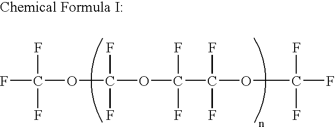
- After the pattern exposure, as shown in FIG. 3C, the resist
film 302 is baked with a hot plate at a temperature of 100° C. for 60 seconds, and the resultant resist film is developed with a 2.38 wt % tetramethylammonium hydroxide developer (alkaline developer). In this manner, a resistpattern 305 made of theunexposed portion 302 b of the resistfilm 302 and having a line width of 0.06 μm can be formed in a good shape as shown in FIG. 3D. - In
Embodiment 3, although a small amount of acid is generated from the acid generator also in theunexposed portion 302 b because leakage light of the exposinglight 304 enters theunexposed portion 302 b of the resistfilm 302, since the pattern exposure is carried out with thesolution 303 including the basic polymer supplied onto the resistfilm 302, the small amount of acid generated in theunexposed portion 302 b is neutralized by the basic polymer included in thesolution 303. Therefore, theunexposed portion 302 b remains insoluble in the alkaline developer. On the other hand, since the amount of acid generated from the acid generator in the exposedportion 302 a of the resistfilm 302 is large, even though the acid generated in the exposedportion 302 a is neutralized by the basic polymer included in thesolution 303, the influence of this neutralization is small. Therefore, the exposedportion 302 a of the resistfilm 302 is easily dissolved in the alkaline developer. Accordingly, the contrast between the exposedportion 302 a and theunexposed portion 302 b of the resistfilm 302 can be largely improved, resulting in forming the resistpattern 305 in a good shape. - A pattern formation method according to
Embodiment 4 of the invention will now be described with reference to FIGS. 4A through 4D. - First, a negative chemically amplified resist material having the following composition is prepared:
- Base polymer: poly((styrenehexafluoroisopropylalcohol)-(α-trifluoromethylacrylic acid)) (wherein styrenehexafluoroisopropyl alcohol:α-trifluoromethylacrylic acid=40 mol %:60 mol %) . . . 2 g
- Crosslinking agent: 1,3,5-N-(dimethoxymethyl)melamine . . . 0.7 g
- Acid generator: triphenylsulfonium triflate . . . 0.08 g
- Solvent: propylene glycol monomethyl ether acetate . . . 20 g
- Next, as shown in FIG. 4A, the aforementioned chemically amplified resist material is applied on a
substrate 401 so as to form a resistfilm 402 with a thickness of 0.20 μm. - Then, as shown in FIG. 4B, while supplying, onto the resist
film 402, asolution 403 of perfluoropolyether including 0.15 wt % of polyaniline (a basic polymer), pattern exposure is carried out by irradiating the resistfilm 402 with exposinglight 404 of F2 laser with NA of 0.60 through a mask not shown. Thus, an exposedportion 402 a of the resistfilm 402 becomes insoluble in an alkaline developer due to the function of the crosslinking agent because an acid is generated from the acid generator therein while anunexposed portion 402 b of the resistfilm 402 remains soluble in an alkaline developer because no acid is generated from the acid generator therein. - After the pattern exposure, as shown in FIG. 4C, the resist
film 402 is baked with a hot plate at a temperature of 110° C. for 60 seconds, and the resultant resist film is developed with a 2.38 wt % tetramethylammonium hydroxide developer (alkaline developer). In this manner, a resistpattern 405 made of the exposedportion 402 a of the resistfilm 402 and having a line width of 0.06 μm can be formed in a good shape as shown in FIG. 4D. - In
Embodiment 4, although a small amount of acid is generated from the acid generator also in theunexposed portion 402 b because leakage light of the exposinglight 404 enters theunexposed portion 402 b of the resistfilm 402, since the pattern exposure is carried out with thesolution 403 including the basic polymer supplied onto the resistfilm 402, the small amount of acid generated in theunexposed portion 402 b is neutralized by the basic polymer included in thesolution 403. Therefore, theunexposed portion 402 b remains soluble in the alkaline developer. On the other hand, since the amount of acid generated from the acid generator in the exposedportion 402 a of the resistfilm 402 is large, even though the acid generated in the exposedportion 402 a is neutralized by the basic polymer included in thesolution 403, the influence of this neutralization is small. Therefore, the exposedportion 402 a of the resistfilm 402 becomes insoluble in the alkaline developer due to the function of the crosslinking agent. Accordingly, the contrast between the exposedportion 402 a and theunexposed portion 402 b of the resistfilm 402 can be largely improved, resulting in forming the resistpattern 405 in a good shape. - In each of
Embodiments solution - A pattern formation method according to
Embodiment 5 of the invention will now be described with reference to FIGS. 5A through 5D. - First, a positive chemically amplified resist material having the following composition is prepared:
- Base polymer: poly((styrenehexafluoroisopropylalcohol)-(α-trifluoromethyl t-butylacrylate)) (wherein styrenehexafluoroisopropylalcohol:α-trifluoromethyl t-butylacrylate=40 mol %:60 mol %) . . . 2 g
- Acid generator: triphenylsulfonium triflate . . . 0.08 g
- Solvent: propylene glycol monomethyl ether acetate . . . 20 g
- Next, as shown in FIG. 5A, the aforementioned chemically amplified resist material is applied on a
substrate 501 so as to form a resistfilm 502 with a thickness of 0.35 μm. - Then, as shown in FIG. 5B, while supplying, onto the resist
film 502, asolution 503 of water including 0.15 wt % of O-acryloylacetophenone oxime (a compound for generating a base through irradiation with light), pattern exposure is carried out by irradiating the resistfilm 502 with exposinglight 504 of ArF excimer laser with NA of 0.65 through a mask not shown. Thus, an exposedportion 502 a of the resistfilm 502 becomes soluble in an alkaline developer because an acid is generated from the acid generator therein while anunexposed portion 502 b of the resistfilm 502 remains insoluble in an alkaline developer because no acid is generated from the acid generator therein. - After the pattern exposure, as shown in FIG. 5C, the resist
film 502 is baked with a hot plate at a temperature of 110°0 C. for 60 seconds, and the resultant resist film is developed with a 2.38 wt % tetramethylammonium hydroxide developer (alkaline developer). In this manner, a resistpattern 505 made of theunexposed portion 502 b of the resistfilm 502 and having a line width of 0.09 μm can be formed in a good shape as shown in FIG. 5D - In
Embodiment 5, although a small amount of acid is generated from the acid generator also in theunexposed portion 502 b because leakage light of the exposinglight 504 enters theunexposed portion 502 b of the resistfilm 502, since the pattern exposure is carried out with thesolution 503 including the compound for generating a base through irradiation with light supplied onto the resistfilm 502, the small amount of acid generated in theunexposed portion 502 b is neutralized by the base generated from the compound for generating a base through irradiation with light included in thesolution 503. Therefore, theunexposed portion 502 b remains insoluble in the alkaline developer. On the other hand, since the amount of acid generated from the acid generator in the exposedportion 502 a of the resistfilm 502 is large, even though the acid generated in the exposedportion 502 a is neutralized by the base generated from the compound for generating a base through irradiation with light included in thesolution 503, the influence of this neutralization is small. Therefore, the exposedportion 502 a of the resistfilm 502 is easily dissolved in the alkaline developer. Accordingly, the contrast between the exposedportion 502 a and theunexposed portion 502 b of the resistfilm 502 can be largely improved, resulting in forming the resistpattern 505 in a good shape. - In
Embodiment 5, the compound for generating a base through irradiation with light to be included in thesolution 503 can be an O-acyl oxime such as O-acryloylacetophenone oxime or O-acryloylacetonaphthone oxime. The content of the compound for generating a base through irradiation with light is generally approximately 0.01 through 0.02 wt %, and may be larger or smaller than this. - A pattern formation method according to Embodiment 6 of the invention will now be described with reference to FIGS. 6A through 6D.
- First, a positive chemically amplified resist material having the following composition is prepared:
- Base polymer: poly((styrenehexafluoroisopropylalcohol)-(α-trifluoromethyl t-butylacrylate)) (wherein styrenehexafluoroisopropylalcohol:α-trifluoromethyl t-butylacrylate=40 mol %:60 mol %) . . . 2 g
- Acid generator: triphenylsulfonium triflate . . . 0.08 g
- Solvent: propylene glycol monomethyl ether acetate . . . 20 g
- Next, as shown in FIG. 6A, the aforementioned chemically amplified resist material is applied on a
substrate 601 so as to form a resistfilm 602 with a thickness of 0.20 μm. - Then, as shown in FIG. 6B, while supplying, onto the resist
film 602, asolution 603 of perfluoropolyether including 0.02 wt % of p-phenacylsulfonylstyrene (a compound for generating a base through application of heat), pattern exposure is carried out by irradiating the resistfilm 602 with exposinglight 604 of F2 laser with NA of 0.60 through a mask not shown. Thus, an exposedportion 602 a of the resistfilm 602 becomes soluble in an alkaline developer because an acid is generated from the acid generator therein while anunexposed portion 602 b of the resistfilm 602 remains insoluble in an alkaline developer because no acid is generated from the acid generator therein. - After the pattern exposure, as shown in FIG. 6C, the resist
film 602 is baked with a hot plate at a temperature of 100° C. for 60 seconds, and the resultant resist film is developed with a 2.38 wt % tetramethylammonium hydroxide developer (alkaline developer). In this manner, a resistpattern 605 made of theunexposed portion 602 b of the resistfilm 602 and having a line width of 0.06 μm can be formed in a good shape as shown in FIG. 6D. - In Embodiment 6, although a small amount of acid is generated from the acid generator also in the
unexposed portion 602 b because leakage light of the exposinglight 604 enters theunexposed portion 602 b of the resistfilm 602, since the pattern exposure is carried out with thesolution 603 including the compound for generating a base through application of heat supplied onto the resistfilm 602, the small amount of acid generated in theunexposed portion 602 b is neutralized by the base generated from the compound for generating a base included in thesolution 603 owing to heat caused by light energy. Therefore, theunexposed portion 602 b remains insoluble in the alkaline developer. On the other hand, since the amount of acid generated from the acid generator in the exposedportion 602 a of the resistfilm 602 is large, even though the acid generated in the exposedportion 602 a is neutralized by the base generated from the compound for generating a base included in thesolution 603 owing to the heat caused by the light energy, the influence of this neutralization is small. Therefore, the exposedportion 602 a of the resistfilm 602 is easily dissolved in the alkaline developer. Accordingly, the contrast between the exposedportion 602 a and theunexposed portion 602 b of the resistfilm 602 can be largely improved, resulting in forming the resistpattern 605 in a good shape. - In Embodiment 6, the compound for generating a base through application of heat to be included in the
solution 603 is not limited to p-phnacylsulfonylstyrene but can be another acylsulfonyl. The content of the compound for generating a base through application of heat is generally approximately 0.01 through 0.02 wt %, and may be larger or smaller than this.
Claims (34)
Applications Claiming Priority (2)
| Application Number | Priority Date | Filing Date | Title |
|---|---|---|---|
| JP2003-177889 | 2003-06-23 | ||
| JP2003177889A JP4029064B2 (en) | 2003-06-23 | 2003-06-23 | Pattern formation method |
Publications (2)
| Publication Number | Publication Date |
|---|---|
| US20040259040A1 true US20040259040A1 (en) | 2004-12-23 |
| US7135273B2 US7135273B2 (en) | 2006-11-14 |
Family
ID=33516296
Family Applications (1)
| Application Number | Title | Priority Date | Filing Date |
|---|---|---|---|
| US10/713,217 Expired - Fee Related US7135273B2 (en) | 2003-06-23 | 2003-11-17 | Pattern formation method |
Country Status (3)
| Country | Link |
|---|---|
| US (1) | US7135273B2 (en) |
| JP (1) | JP4029064B2 (en) |
| CN (1) | CN1285100C (en) |
Cited By (101)
| Publication number | Priority date | Publication date | Assignee | Title |
|---|---|---|---|---|
| US20040013978A1 (en) * | 2002-07-15 | 2004-01-22 | Matsushita Electric Industrial Co., Ltd. | Pattern formation material and pattern formation method |
| US20050007569A1 (en) * | 2003-05-13 | 2005-01-13 | Asml Netherlands B.V. | Lithographic apparatus and device manufacturing method |
| US20050128445A1 (en) * | 2003-10-28 | 2005-06-16 | Asml Netherlands B.V. | Lithographic apparatus and device manufacturing method |
| US20050175940A1 (en) * | 2004-02-11 | 2005-08-11 | Asml Netherlands B.V. | Device manufacturing method and a substrate |
| US20050175776A1 (en) * | 2003-11-14 | 2005-08-11 | Asml Netherlands B.V. | Lithographic apparatus and device manufacturing method |
| US20050219489A1 (en) * | 2002-12-10 | 2005-10-06 | Nikon Corporation | Exposure apparatus and method for producing device |
| US20050219490A1 (en) * | 2002-12-10 | 2005-10-06 | Nikon Corporation | Exposure apparatus and method for producing device |
| US20050219488A1 (en) * | 2002-12-10 | 2005-10-06 | Nikon Corporation | Exposure apparatus and method for producing device |
| US20050225734A1 (en) * | 2004-04-08 | 2005-10-13 | Asml Netherlands B.V. | Lithographic apparatus and device manufacturing method |
| US20050231694A1 (en) * | 2004-04-14 | 2005-10-20 | Asml Netherlands B.V. | Lithographic apparatus and device manufacturing method |
| US20050237504A1 (en) * | 2002-12-10 | 2005-10-27 | Nikon Corporation | Exposure apparatus, exposure method, and method for producing device |
| US20050259232A1 (en) * | 2004-05-18 | 2005-11-24 | Asml Netherlands B.V. | Lithographic apparatus and device manufacturing method |
| US20050264774A1 (en) * | 2002-12-10 | 2005-12-01 | Nikon Corporation | Exposure apparatus and method for producing device |
| US20050280791A1 (en) * | 2003-02-26 | 2005-12-22 | Nikon Corporation | Exposure apparatus, exposure method, and method for producing device |
| US20060012765A1 (en) * | 2003-03-25 | 2006-01-19 | Nikon Corporation | Exposure apparatus and device fabrication method |
| US20060017900A1 (en) * | 2003-04-17 | 2006-01-26 | Nikon Corporation | Optical arrangement of autofocus elements for use with immersion lithography |
| US20060023189A1 (en) * | 2002-11-12 | 2006-02-02 | Asml Netherlands B.V. | Lithographic apparatus and device manufacturing method |
| US20060023184A1 (en) * | 2003-04-09 | 2006-02-02 | Nikon Corporation | Immersion lithography fluid control system |
| US20060023188A1 (en) * | 2003-04-07 | 2006-02-02 | Nikon Corporation | Exposure apparatus and method for manufacturing device |
| US20060023183A1 (en) * | 2003-04-11 | 2006-02-02 | Nikon Corporation | Liquid jet and recovery system for immersion lithography |
| US20060023181A1 (en) * | 2003-04-10 | 2006-02-02 | Nikon Corporation | Run-off path to collect liquid for an immersion lithography apparatus |
| US20060023187A1 (en) * | 2003-04-10 | 2006-02-02 | Nikon Corporation | Environmental system including an electro-osmotic element for an immersion lithography apparatus |
| US20060023182A1 (en) * | 2003-04-10 | 2006-02-02 | Nikon Corporation | Environmental system including a transport region for an immersion lithography apparatus |
| US20060028632A1 (en) * | 2003-04-10 | 2006-02-09 | Nikon Corporation | Environmental system including vacuum scavenge for an immersion lithography apparatus |
| US20060033894A1 (en) * | 2003-04-11 | 2006-02-16 | Nikon Corporation | Apparatus and method for maintaining immersion fluid in the gap under the projection lens during wafer exchange in an immersion lithography machine |
| US20060061747A1 (en) * | 2003-05-15 | 2006-03-23 | Nikon Corporation | Exposure apparatus and device manufacturing method |
| US20060077367A1 (en) * | 2003-05-23 | 2006-04-13 | Nikon Corporation | Exposure apparatus and method for producing device |
| US20060082744A1 (en) * | 2003-05-28 | 2006-04-20 | Nikon Corporation | Exposure method, exposure apparatus, and method for producing device |
| US20060092533A1 (en) * | 2003-07-01 | 2006-05-04 | Nikon Corporation | Using isotopically specified fluids as optical elements |
| US20060098177A1 (en) * | 2003-05-23 | 2006-05-11 | Nikon Corporation | Exposure method, exposure apparatus, and exposure method for producing device |
| US20060114445A1 (en) * | 2003-06-19 | 2006-06-01 | Nikon Corporation | Exposure apparatus, and device manufacturing method |
| US20060119820A1 (en) * | 2002-12-10 | 2006-06-08 | Nikon Corporation | Exposure apparatus and device manufacturing method |
| US20060119818A1 (en) * | 2003-07-09 | 2006-06-08 | Nikon Corporation | Exposure apparatus and method for manufacturing device |
| US20060139614A1 (en) * | 2003-06-13 | 2006-06-29 | Nikon Corporation | Exposure method, substrate stage, exposure apparatus, and device manufacturing method |
| US20060146305A1 (en) * | 2003-07-28 | 2006-07-06 | Nikon Corporation | Exposure apparatus, method for producing device, and method for controlling exposure apparatus |
| US20060154183A1 (en) * | 2002-12-10 | 2006-07-13 | Nikon Corporation | Exposure apparatus and method for producing device |
| US20060152697A1 (en) * | 2003-09-03 | 2006-07-13 | Nikon Corporation | Apparatus and method for providing fluid for immersion lithography |
| US20060246373A1 (en) * | 2005-05-01 | 2006-11-02 | Rohm And Haas Electronic Materials Llc | Compositions and processes for immersion lithography |
| US20070066452A1 (en) * | 2005-09-22 | 2007-03-22 | William Marshall | Recliner exerciser |
| US20070070316A1 (en) * | 2004-01-20 | 2007-03-29 | Albrecht Ehrmann | Microlithographic projection exposure apparatus and measuring device for a projection lens |
| US20070103655A1 (en) * | 2003-07-28 | 2007-05-10 | Asml Netherlands B.V. | Lithographic apparatus, device manufacturing method and a substrate |
| US20070128482A1 (en) * | 2005-12-06 | 2007-06-07 | Lg Electronics Inc. | Power supply apparatus and method for line connection type fuel cell system |
| US20070171390A1 (en) * | 2003-04-11 | 2007-07-26 | Nikon Corporation | Cleanup method for optics in immersion lithography |
| US20070190448A1 (en) * | 2004-03-05 | 2007-08-16 | Keita Ishiduka | Positive-type resist composition for liquid immersion lithography and method for forming resist pattern |
| US7301607B2 (en) | 2003-07-08 | 2007-11-27 | Nikon Corporation | Wafer table for immersion lithography |
| US7372541B2 (en) | 2002-11-12 | 2008-05-13 | Asml Netherlands B.V. | Lithographic apparatus and device manufacturing method |
| US7394521B2 (en) | 2003-12-23 | 2008-07-01 | Asml Netherlands B.V. | Lithographic apparatus and device manufacturing method |
| US7397533B2 (en) | 2004-12-07 | 2008-07-08 | Asml Netherlands B.V. | Lithographic apparatus and device manufacturing method |
| US7411653B2 (en) | 2003-10-28 | 2008-08-12 | Asml Netherlands B.V. | Lithographic apparatus |
| US20080193872A1 (en) * | 2006-10-30 | 2008-08-14 | Rohm And Haas Electronic Materials Llc | Compositions and processes for immersion lithography |
| US7453078B2 (en) | 2005-02-28 | 2008-11-18 | Asml Netherlands B.V. | Sensor for use in a lithographic apparatus |
| US7463330B2 (en) | 2004-07-07 | 2008-12-09 | Asml Netherlands B.V. | Lithographic apparatus and device manufacturing method |
| WO2009009070A1 (en) * | 2007-07-09 | 2009-01-15 | E. I. Du Pont De Nemours And Company | Compositions and methods for creating electronic circuitry |
| US7483118B2 (en) | 2003-07-28 | 2009-01-27 | Asml Netherlands B.V. | Lithographic projection apparatus and device manufacturing method |
| US20090040389A1 (en) * | 2007-08-09 | 2009-02-12 | Mstar Semiconductor, Inc | Gamma correction apparatus |
| US7508490B2 (en) | 2003-07-09 | 2009-03-24 | Nikon Corporation | Exposure apparatus and device manufacturing method |
| US7515249B2 (en) | 2003-10-08 | 2009-04-07 | Zao Nikon Co., Ltd. | Substrate carrying apparatus, exposure apparatus, and device manufacturing method |
| US20090117489A1 (en) * | 2007-11-05 | 2009-05-07 | Rohm And Haas Electronics Materials Llc | Compositons and processes for immersion lithography |
| US7589822B2 (en) | 2004-02-02 | 2009-09-15 | Nikon Corporation | Stage drive method and stage unit, exposure apparatus, and device manufacturing method |
| US7593093B2 (en) | 2002-11-12 | 2009-09-22 | Asml Netherlands B.V. | Lithographic apparatus and device manufacturing method |
| US7602470B2 (en) | 2004-08-19 | 2009-10-13 | Asml Netherlands B.V. | Lithographic apparatus and device manufacturing method |
| US7619715B2 (en) | 2003-07-09 | 2009-11-17 | Nikon Corporation | Coupling apparatus, exposure apparatus, and device fabricating method |
| US7626685B2 (en) | 2008-03-26 | 2009-12-01 | Samsung Electronics Co., Ltd. | Distance measuring sensors including vertical photogate and three-dimensional color image sensors including distance measuring sensors |
| US7684008B2 (en) | 2003-06-11 | 2010-03-23 | Asml Netherlands B.V. | Lithographic apparatus and device manufacturing method |
| US20100182576A1 (en) * | 2003-12-23 | 2010-07-22 | Asml Netherlands B.V. | Lithographic apparatus and device manufacturing method |
| US7779781B2 (en) | 2003-07-31 | 2010-08-24 | Asml Netherlands B.V. | Lithographic apparatus and device manufacturing method |
| US7843550B2 (en) | 2003-07-25 | 2010-11-30 | Nikon Corporation | Projection optical system inspecting method and inspection apparatus, and a projection optical system manufacturing method |
| US7880860B2 (en) | 2004-12-20 | 2011-02-01 | Asml Netherlands B.V. | Lithographic apparatus and device manufacturing method |
| US7898645B2 (en) | 2003-10-08 | 2011-03-01 | Zao Nikon Co., Ltd. | Substrate transport apparatus and method, exposure apparatus and exposure method, and device fabricating method |
| US7907255B2 (en) | 2003-08-29 | 2011-03-15 | Asml Netherlands B.V. | Lithographic apparatus and device manufacturing method |
| US7924402B2 (en) | 2003-09-19 | 2011-04-12 | Nikon Corporation | Exposure apparatus and device manufacturing method |
| US7924403B2 (en) | 2005-01-14 | 2011-04-12 | Asml Netherlands B.V. | Lithographic apparatus and device and device manufacturing method |
| US20110104375A1 (en) * | 2006-03-03 | 2011-05-05 | Craig Waldron | Biocide composition comprising pyrithione and pyrrole derivatives |
| US7982857B2 (en) | 2003-12-15 | 2011-07-19 | Nikon Corporation | Stage apparatus, exposure apparatus, and exposure method with recovery device having lyophilic portion |
| US7990516B2 (en) | 2004-02-03 | 2011-08-02 | Nikon Corporation | Immersion exposure apparatus and device manufacturing method with liquid detection apparatus |
| US7995186B2 (en) | 2003-10-08 | 2011-08-09 | Zao Nikon Co., Ltd. | Substrate conveyance device and substrate conveyance method, exposure apparatus and exposure method, device manufacturing method |
| US8039807B2 (en) | 2003-09-29 | 2011-10-18 | Nikon Corporation | Exposure apparatus, exposure method, and method for producing device |
| US8054447B2 (en) | 2003-12-03 | 2011-11-08 | Nikon Corporation | Exposure apparatus, exposure method, method for producing device, and optical part |
| US8054448B2 (en) | 2004-05-04 | 2011-11-08 | Nikon Corporation | Apparatus and method for providing fluid for immersion lithography |
| US8111373B2 (en) | 2004-03-25 | 2012-02-07 | Nikon Corporation | Exposure apparatus and device fabrication method |
| US8120763B2 (en) | 2002-12-20 | 2012-02-21 | Carl Zeiss Smt Gmbh | Device and method for the optical measurement of an optical system by using an immersion fluid |
| US8130361B2 (en) | 2003-10-09 | 2012-03-06 | Nikon Corporation | Exposure apparatus, exposure method, and method for producing device |
| US8154708B2 (en) | 2003-06-09 | 2012-04-10 | Asml Netherlands B.V. | Lithographic apparatus and device manufacturing method |
| US8237911B2 (en) | 2007-03-15 | 2012-08-07 | Nikon Corporation | Apparatus and methods for keeping immersion fluid adjacent to an optical assembly during wafer exchange in an immersion lithography machine |
| USRE43576E1 (en) | 2005-04-08 | 2012-08-14 | Asml Netherlands B.V. | Dual stage lithographic apparatus and device manufacturing method |
| US8305553B2 (en) | 2004-08-18 | 2012-11-06 | Nikon Corporation | Exposure apparatus and device manufacturing method |
| US8363206B2 (en) | 2006-05-09 | 2013-01-29 | Carl Zeiss Smt Gmbh | Optical imaging device with thermal attenuation |
| US8384874B2 (en) | 2004-07-12 | 2013-02-26 | Nikon Corporation | Immersion exposure apparatus and device manufacturing method to detect if liquid on base member |
| US8449949B2 (en) | 2007-07-09 | 2013-05-28 | E. I. Du Pont De Nemours And Company | Compositions and methods for creating electronic circuitry |
| US8520184B2 (en) | 2004-06-09 | 2013-08-27 | Nikon Corporation | Immersion exposure apparatus and device manufacturing method with measuring device |
| US8654305B2 (en) | 2007-02-15 | 2014-02-18 | Asml Holding N.V. | Systems and methods for insitu lens cleaning in immersion lithography |
| US8692973B2 (en) | 2005-01-31 | 2014-04-08 | Nikon Corporation | Exposure apparatus and method for producing device |
| US8817226B2 (en) | 2007-02-15 | 2014-08-26 | Asml Holding N.V. | Systems and methods for insitu lens cleaning using ozone in immersion lithography |
| US8941810B2 (en) | 2005-12-30 | 2015-01-27 | Asml Netherlands B.V. | Lithographic apparatus and device manufacturing method |
| US9176393B2 (en) | 2008-05-28 | 2015-11-03 | Asml Netherlands B.V. | Lithographic apparatus and a method of operating the apparatus |
| US9223224B2 (en) | 2003-08-29 | 2015-12-29 | Nikon Corporation | Exposure apparatus with component from which liquid is protected and/or removed and device fabricating method |
| US9256136B2 (en) | 2010-04-22 | 2016-02-09 | Asml Netherlands B.V. | Fluid handling structure, lithographic apparatus and device manufacturing method involving gas supply |
| US9429495B2 (en) | 2004-06-04 | 2016-08-30 | Carl Zeiss Smt Gmbh | System for measuring the image quality of an optical imaging system |
| US9482966B2 (en) | 2002-11-12 | 2016-11-01 | Asml Netherlands B.V. | Lithographic apparatus and device manufacturing method |
| US9746781B2 (en) | 2005-01-31 | 2017-08-29 | Nikon Corporation | Exposure apparatus and method for producing device |
| US10503084B2 (en) | 2002-11-12 | 2019-12-10 | Asml Netherlands B.V. | Lithographic apparatus and device manufacturing method |
Families Citing this family (6)
| Publication number | Priority date | Publication date | Assignee | Title |
|---|---|---|---|---|
| WO2005081063A1 (en) * | 2004-02-20 | 2005-09-01 | Daikin Industries, Ltd. | Resist laminate used for immersion lithography |
| JP2006024692A (en) | 2004-07-07 | 2006-01-26 | Toshiba Corp | Resist pattern forming method |
| CN100461004C (en) * | 2005-08-05 | 2009-02-11 | 台湾积体电路制造股份有限公司 | Immersion lithography method and processing method thereof |
| JP5299347B2 (en) * | 2010-04-26 | 2013-09-25 | 株式会社ニコン | Exposure apparatus, liquid supply method, and device manufacturing method |
| JP5024419B2 (en) * | 2010-04-26 | 2012-09-12 | 株式会社ニコン | Exposure apparatus, liquid supply method, and device manufacturing method |
| US8856695B1 (en) | 2013-03-14 | 2014-10-07 | Samsung Electronics Co., Ltd. | Method for generating post-OPC layout in consideration of top loss of etch mask layer |
Citations (8)
| Publication number | Priority date | Publication date | Assignee | Title |
|---|---|---|---|---|
| US5460096A (en) * | 1993-05-26 | 1995-10-24 | Comet Gmbh Pyrotechnik-Apparatebau | Gas generator, particularly a mechanically triggerable gas generator |
| US5585595A (en) * | 1994-05-19 | 1996-12-17 | Comet Gmbh Pyrotechnik-Apparatebau | Device for simulating weapons firing and/or hit indication |
| US6101950A (en) * | 1996-03-14 | 2000-08-15 | Comet Gmbh | Projectile simulation means |
| US20020144620A1 (en) * | 2001-04-06 | 2002-10-10 | Comet Gmbh Pyrotechnik-Apparatebau | Closure for a pyrotechnic unit |
| US20020163629A1 (en) * | 2001-05-07 | 2002-11-07 | Michael Switkes | Methods and apparatus employing an index matching medium |
| US20060162602A1 (en) * | 2005-01-04 | 2006-07-27 | Comet Gmbh Pyrotechnik-Apparatebau | Device for generating pyrotechnic effects |
| US20070199469A1 (en) * | 2006-02-28 | 2007-08-30 | Zahn Arthur D | Apparatus for production of pyrotechnic effects |
| US20080000377A1 (en) * | 2006-06-30 | 2008-01-03 | Thomas Doyle | Simulating An Explosion Of An Improvised Explosive Device |
-
2003
- 2003-06-23 JP JP2003177889A patent/JP4029064B2/en not_active Expired - Fee Related
- 2003-11-17 US US10/713,217 patent/US7135273B2/en not_active Expired - Fee Related
- 2003-12-12 CN CN200310120570.6A patent/CN1285100C/en not_active Expired - Fee Related
Patent Citations (8)
| Publication number | Priority date | Publication date | Assignee | Title |
|---|---|---|---|---|
| US5460096A (en) * | 1993-05-26 | 1995-10-24 | Comet Gmbh Pyrotechnik-Apparatebau | Gas generator, particularly a mechanically triggerable gas generator |
| US5585595A (en) * | 1994-05-19 | 1996-12-17 | Comet Gmbh Pyrotechnik-Apparatebau | Device for simulating weapons firing and/or hit indication |
| US6101950A (en) * | 1996-03-14 | 2000-08-15 | Comet Gmbh | Projectile simulation means |
| US20020144620A1 (en) * | 2001-04-06 | 2002-10-10 | Comet Gmbh Pyrotechnik-Apparatebau | Closure for a pyrotechnic unit |
| US20020163629A1 (en) * | 2001-05-07 | 2002-11-07 | Michael Switkes | Methods and apparatus employing an index matching medium |
| US20060162602A1 (en) * | 2005-01-04 | 2006-07-27 | Comet Gmbh Pyrotechnik-Apparatebau | Device for generating pyrotechnic effects |
| US20070199469A1 (en) * | 2006-02-28 | 2007-08-30 | Zahn Arthur D | Apparatus for production of pyrotechnic effects |
| US20080000377A1 (en) * | 2006-06-30 | 2008-01-03 | Thomas Doyle | Simulating An Explosion Of An Improvised Explosive Device |
Cited By (544)
| Publication number | Priority date | Publication date | Assignee | Title |
|---|---|---|---|---|
| US6936401B2 (en) * | 2002-07-15 | 2005-08-30 | Matsushita Electric Industrial Co., Ltd. | Pattern formation material and pattern formation method |
| US20040013978A1 (en) * | 2002-07-15 | 2004-01-22 | Matsushita Electric Industrial Co., Ltd. | Pattern formation material and pattern formation method |
| US10191389B2 (en) | 2002-11-12 | 2019-01-29 | Asml Netherlands B.V. | Lithographic apparatus and device manufacturing method |
| US9482966B2 (en) | 2002-11-12 | 2016-11-01 | Asml Netherlands B.V. | Lithographic apparatus and device manufacturing method |
| US9091940B2 (en) | 2002-11-12 | 2015-07-28 | Asml Netherlands B.V. | Lithographic apparatus and method involving a fluid inlet and a fluid outlet |
| US7388648B2 (en) | 2002-11-12 | 2008-06-17 | Asml Netherlands B.V. | Lithographic projection apparatus |
| US7372541B2 (en) | 2002-11-12 | 2008-05-13 | Asml Netherlands B.V. | Lithographic apparatus and device manufacturing method |
| US10222706B2 (en) | 2002-11-12 | 2019-03-05 | Asml Netherlands B.V. | Lithographic apparatus and device manufacturing method |
| US10503084B2 (en) | 2002-11-12 | 2019-12-10 | Asml Netherlands B.V. | Lithographic apparatus and device manufacturing method |
| US10962891B2 (en) | 2002-11-12 | 2021-03-30 | Asml Netherlands B.V. | Lithographic apparatus and device manufacturing method |
| US10788755B2 (en) | 2002-11-12 | 2020-09-29 | Asml Netherlands B.V. | Lithographic apparatus and device manufacturing method |
| US7593093B2 (en) | 2002-11-12 | 2009-09-22 | Asml Netherlands B.V. | Lithographic apparatus and device manufacturing method |
| US8797503B2 (en) | 2002-11-12 | 2014-08-05 | Asml Netherlands B.V. | Lithographic apparatus and device manufacturing method with a liquid inlet above an aperture of a liquid confinement structure |
| US9740107B2 (en) | 2002-11-12 | 2017-08-22 | Asml Netherlands B.V. | Lithographic apparatus and device manufacturing method |
| US9366972B2 (en) | 2002-11-12 | 2016-06-14 | Asml Netherlands B.V. | Lithographic apparatus and device manufacturing method |
| US7593092B2 (en) | 2002-11-12 | 2009-09-22 | Asml Netherlands B.V. | Lithographic apparatus and device manufacturing method |
| US8208120B2 (en) | 2002-11-12 | 2012-06-26 | Asml Netherlands B.V. | Lithographic apparatus and device manufacturing method |
| US20060023189A1 (en) * | 2002-11-12 | 2006-02-02 | Asml Netherlands B.V. | Lithographic apparatus and device manufacturing method |
| US8558989B2 (en) | 2002-11-12 | 2013-10-15 | Asml Netherlands B.V. | Lithographic apparatus and device manufacturing method |
| US10261428B2 (en) | 2002-11-12 | 2019-04-16 | Asml Netherlands B.V. | Lithographic apparatus and device manufacturing method |
| US10620545B2 (en) | 2002-11-12 | 2020-04-14 | Asml Netherlands B.V. | Lithographic apparatus and device manufacturing method |
| US9057967B2 (en) | 2002-11-12 | 2015-06-16 | Asml Netherlands B.V. | Lithographic apparatus and device manufacturing method |
| US8472002B2 (en) | 2002-11-12 | 2013-06-25 | Asml Netherlands B.V. | Lithographic apparatus and device manufacturing method |
| US7982850B2 (en) | 2002-11-12 | 2011-07-19 | Asml Netherlands B.V. | Immersion lithographic apparatus and device manufacturing method with gas supply |
| US20070024832A1 (en) * | 2002-12-10 | 2007-02-01 | Nikon Corporation | Exposure apparatus and method for producing device |
| US20070115448A1 (en) * | 2002-12-10 | 2007-05-24 | Nikon Corporation | Exposure apparatus and device manufacturing method |
| US8034539B2 (en) | 2002-12-10 | 2011-10-11 | Nikon Corporation | Exposure apparatus and method for producing device |
| US8294876B2 (en) | 2002-12-10 | 2012-10-23 | Nikon Corporation | Exposure apparatus and device manufacturing method |
| US8004650B2 (en) | 2002-12-10 | 2011-08-23 | Nikon Corporation | Exposure apparatus and device manufacturing method |
| US7436487B2 (en) | 2002-12-10 | 2008-10-14 | Nikon Corporation | Exposure apparatus and method for producing device |
| US7948604B2 (en) | 2002-12-10 | 2011-05-24 | Nikon Corporation | Exposure apparatus and method for producing device |
| US7436486B2 (en) | 2002-12-10 | 2008-10-14 | Nikon Corporation | Exposure apparatus and device manufacturing method |
| US8089611B2 (en) | 2002-12-10 | 2012-01-03 | Nikon Corporation | Exposure apparatus and method for producing device |
| US20060098178A1 (en) * | 2002-12-10 | 2006-05-11 | Nikon Corporation | Exposure apparatus, exposure method, and method for producing device |
| US7379158B2 (en) | 2002-12-10 | 2008-05-27 | Nikon Corporation | Exposure apparatus and method for producing device |
| US7911582B2 (en) | 2002-12-10 | 2011-03-22 | Nikon Corporation | Exposure apparatus and device manufacturing method |
| US20050219489A1 (en) * | 2002-12-10 | 2005-10-06 | Nikon Corporation | Exposure apparatus and method for producing device |
| US20060119820A1 (en) * | 2002-12-10 | 2006-06-08 | Nikon Corporation | Exposure apparatus and device manufacturing method |
| US7446851B2 (en) | 2002-12-10 | 2008-11-04 | Nikon Corporation | Exposure apparatus and device manufacturing method |
| US20060126043A1 (en) * | 2002-12-10 | 2006-06-15 | Nikon Corporation | Exposure apparatus and method for producing device |
| US20060126044A1 (en) * | 2002-12-10 | 2006-06-15 | Nikon Corporation | Exposure apparatus and method for producing device |
| US20060132738A1 (en) * | 2002-12-10 | 2006-06-22 | Nikon Corporation | Exposure apparatus and device manufacturing method |
| US7460207B2 (en) | 2002-12-10 | 2008-12-02 | Nikon Corporation | Exposure apparatus and method for producing device |
| US20060132736A1 (en) * | 2002-12-10 | 2006-06-22 | Nikon Corporation | Exposure apparatus, exposure method, and method for producing device |
| US20050219490A1 (en) * | 2002-12-10 | 2005-10-06 | Nikon Corporation | Exposure apparatus and method for producing device |
| US7466392B2 (en) | 2002-12-10 | 2008-12-16 | Nikon Corporation | Exposure apparatus, exposure method, and method for producing device |
| US20060152699A1 (en) * | 2002-12-10 | 2006-07-13 | Nikon Corporation | Exposure apparatus and method for producing device |
| US20060154183A1 (en) * | 2002-12-10 | 2006-07-13 | Nikon Corporation | Exposure apparatus and method for producing device |
| US7505111B2 (en) | 2002-12-10 | 2009-03-17 | Nikon Corporation | Exposure apparatus and device manufacturing method |
| US20070263196A1 (en) * | 2002-12-10 | 2007-11-15 | Nikon Corporation | Exposure apparatus and device manufacturing method |
| US20060164615A1 (en) * | 2002-12-10 | 2006-07-27 | Nikon Corporation | Exposure apparatus and device manufacturing method |
| US7834976B2 (en) | 2002-12-10 | 2010-11-16 | Nikon Corporation | Exposure apparatus and method for producing device |
| US7817244B2 (en) | 2002-12-10 | 2010-10-19 | Nikon Corporation | Exposure apparatus and method for producing device |
| US20070258063A1 (en) * | 2002-12-10 | 2007-11-08 | Nikon Corporation | Exposure apparatus, exposure method, and method for producing device |
| US20060250596A1 (en) * | 2002-12-10 | 2006-11-09 | Nikon Corporation | Exposure apparatus and method for producing device |
| US20090079950A1 (en) * | 2002-12-10 | 2009-03-26 | Nikon Corporation | Exposure apparatus, exposure method, and method for producing device |
| US20060274294A1 (en) * | 2002-12-10 | 2006-12-07 | Nikon Corporation | Exposure apparatus, exposure method, and method for producing device |
| US7515246B2 (en) | 2002-12-10 | 2009-04-07 | Nikon Corporation | Exposure apparatus, exposure method, and method for producing device |
| US20070035710A1 (en) * | 2002-12-10 | 2007-02-15 | Nikon Corporation | Exposure apparatus, exposure method, and method for producing device |
| US20070035711A1 (en) * | 2002-12-10 | 2007-02-15 | Nikon Corporation | Exposure apparatus and method for producing device |
| US20050219488A1 (en) * | 2002-12-10 | 2005-10-06 | Nikon Corporation | Exposure apparatus and method for producing device |
| US20050237504A1 (en) * | 2002-12-10 | 2005-10-27 | Nikon Corporation | Exposure apparatus, exposure method, and method for producing device |
| US20070171391A1 (en) * | 2002-12-10 | 2007-07-26 | Nikon Corporation | Exposure apparatus and method for producing device |
| US7639343B2 (en) | 2002-12-10 | 2009-12-29 | Nikon Corporation | Exposure apparatus and device manufacturing method |
| US7242455B2 (en) | 2002-12-10 | 2007-07-10 | Nikon Corporation | Exposure apparatus and method for producing device |
| US20050264774A1 (en) * | 2002-12-10 | 2005-12-01 | Nikon Corporation | Exposure apparatus and method for producing device |
| US7589821B2 (en) | 2002-12-10 | 2009-09-15 | Nikon Corporation | Exposure apparatus and device manufacturing method |
| US7589820B2 (en) | 2002-12-10 | 2009-09-15 | Nikon Corporation | Exposure apparatus and method for producing device |
| US20070115447A1 (en) * | 2002-12-10 | 2007-05-24 | Nikon Corporation | Exposure apparatus and device manufacturing method |
| US8836929B2 (en) | 2002-12-20 | 2014-09-16 | Carl Zeiss Smt Gmbh | Device and method for the optical measurement of an optical system by using an immersion fluid |
| US8120763B2 (en) | 2002-12-20 | 2012-02-21 | Carl Zeiss Smt Gmbh | Device and method for the optical measurement of an optical system by using an immersion fluid |
| US10180632B2 (en) | 2003-02-26 | 2019-01-15 | Nikon Corporation | Exposure apparatus, exposure method, and method for producing device |
| US7907254B2 (en) | 2003-02-26 | 2011-03-15 | Nikon Corporation | Exposure apparatus, exposure method, and method for producing device |
| US7542128B2 (en) | 2003-02-26 | 2009-06-02 | Nikon Corporation | Exposure apparatus, exposure method, and method for producing device |
| US7535550B2 (en) | 2003-02-26 | 2009-05-19 | Nikon Corporation | Exposure apparatus, exposure method, and method for producing device |
| US9348239B2 (en) | 2003-02-26 | 2016-05-24 | Nikon Corporation | Exposure apparatus, exposure method, and method for producing device |
| US8736809B2 (en) | 2003-02-26 | 2014-05-27 | Nikon Corporation | Exposure apparatus, exposure method, and method for producing device |
| US7932991B2 (en) | 2003-02-26 | 2011-04-26 | Nikon Corporation | Exposure apparatus, exposure method, and method for producing device |
| US9766555B2 (en) | 2003-02-26 | 2017-09-19 | Nikon Corporation | Exposure apparatus, exposure method, and method for producing device |
| US7907253B2 (en) | 2003-02-26 | 2011-03-15 | Nikon Corporation | Exposure apparatus, exposure method, and method for producing device |
| US7911583B2 (en) | 2003-02-26 | 2011-03-22 | Nikon Corporation | Exposure apparatus, exposure method, and method for producing device |
| US9182684B2 (en) | 2003-02-26 | 2015-11-10 | Nikon Corporation | Exposure apparatus, exposure method, and method for producing device |
| US7268854B2 (en) | 2003-02-26 | 2007-09-11 | Nikon Corporation | Exposure apparatus, exposure method, and method for producing device |
| US20050280791A1 (en) * | 2003-02-26 | 2005-12-22 | Nikon Corporation | Exposure apparatus, exposure method, and method for producing device |
| US20070263186A1 (en) * | 2003-02-26 | 2007-11-15 | Nikon Corporation | Exposure apparatus, exposure method, and method for producing device |
| US8102504B2 (en) | 2003-02-26 | 2012-01-24 | Nikon Corporation | Exposure apparatus, exposure method, and method for producing device |
| US7453550B2 (en) | 2003-02-26 | 2008-11-18 | Nikon Corporation | Exposure apparatus, exposure method, and method for producing device |
| US20070258065A1 (en) * | 2003-02-26 | 2007-11-08 | Nikon Corporation | Exposure apparatus, exposure method, and method for producing device |
| US20070258067A1 (en) * | 2003-02-26 | 2007-11-08 | Nikon Corporation | Exposure apparatus, exposure method, and method for producing device |
| US8558987B2 (en) | 2003-03-25 | 2013-10-15 | Nikon Corporation | Exposure apparatus and device fabrication method |
| US8804095B2 (en) | 2003-03-25 | 2014-08-12 | Nikon Corporation | Exposure apparatus and device fabrication method |
| US20070109516A1 (en) * | 2003-03-25 | 2007-05-17 | Nikon Corporation | Exposure apparatus and device fabrication method |
| US8018570B2 (en) | 2003-03-25 | 2011-09-13 | Nikon Corporation | Exposure apparatus and device fabrication method |
| US20060268249A1 (en) * | 2003-03-25 | 2006-11-30 | Nikon Corporation | Exposure apparatus and device fabrication method |
| US7916272B2 (en) | 2003-03-25 | 2011-03-29 | Nikon Corporation | Exposure apparatus and device fabrication method |
| US20060012765A1 (en) * | 2003-03-25 | 2006-01-19 | Nikon Corporation | Exposure apparatus and device fabrication method |
| US7471371B2 (en) | 2003-03-25 | 2008-12-30 | Nikon Corporation | Exposure apparatus and device fabrication method |
| US8537331B2 (en) | 2003-04-07 | 2013-09-17 | Nikon Corporation | Exposure apparatus and method for manufacturing device |
| US20080291410A1 (en) * | 2003-04-07 | 2008-11-27 | Nikon Corporation | Exposure apparatus and method for manufacturing device |
| US20060033901A1 (en) * | 2003-04-07 | 2006-02-16 | Nikon Corporation | Exposure apparatus and method for manufacturing device |
| US8111375B2 (en) | 2003-04-07 | 2012-02-07 | Nikon Corporation | Exposure apparatus and method for manufacturing device |
| US20060023188A1 (en) * | 2003-04-07 | 2006-02-02 | Nikon Corporation | Exposure apparatus and method for manufacturing device |
| US7480029B2 (en) | 2003-04-07 | 2009-01-20 | Nikon Corporation | Exposure apparatus and method for manufacturing device |
| US20090075211A1 (en) * | 2003-04-09 | 2009-03-19 | Nikon Corporation | Immersion lithography fluid control system |
| US20070263184A1 (en) * | 2003-04-09 | 2007-11-15 | Nikon Corporation | Immersion lithography fluid control system |
| US8797500B2 (en) | 2003-04-09 | 2014-08-05 | Nikon Corporation | Immersion lithography fluid control system changing flow velocity of gas outlets based on motion of a surface |
| US8497973B2 (en) | 2003-04-09 | 2013-07-30 | Nikon Corporation | Immersion lithography fluid control system regulating gas velocity based on contact angle |
| US8102501B2 (en) | 2003-04-09 | 2012-01-24 | Nikon Corporation | Immersion lithography fluid control system using an electric or magnetic field generator |
| US20090075212A1 (en) * | 2003-04-09 | 2009-03-19 | Nikon Corporation | Immersion lithography fluid control system |
| US7339650B2 (en) | 2003-04-09 | 2008-03-04 | Nikon Corporation | Immersion lithography fluid control system that applies force to confine the immersion liquid |
| US20060023184A1 (en) * | 2003-04-09 | 2006-02-02 | Nikon Corporation | Immersion lithography fluid control system |
| US20070268468A1 (en) * | 2003-04-09 | 2007-11-22 | Nikon Corporation | Immersion lithography fluid control system |
| US20070115453A1 (en) * | 2003-04-09 | 2007-05-24 | Nikon Corporation | Immersion lithography fluid control system |
| US9618852B2 (en) | 2003-04-09 | 2017-04-11 | Nikon Corporation | Immersion lithography fluid control system regulating flow velocity of gas based on position of gas outlets |
| US7456930B2 (en) | 2003-04-10 | 2008-11-25 | Nikon Corporation | Environmental system including vacuum scavenge for an immersion lithography apparatus |
| US8836914B2 (en) | 2003-04-10 | 2014-09-16 | Nikon Corporation | Environmental system including vacuum scavenge for an immersion lithography apparatus |
| US8243253B2 (en) | 2003-04-10 | 2012-08-14 | Nikon Corporation | Lyophobic run-off path to collect liquid for an immersion lithography apparatus |
| US9910370B2 (en) | 2003-04-10 | 2018-03-06 | Nikon Corporation | Environmental system including a transport region for an immersion lithography apparatus |
| US20060023181A1 (en) * | 2003-04-10 | 2006-02-02 | Nikon Corporation | Run-off path to collect liquid for an immersion lithography apparatus |
| US8089610B2 (en) | 2003-04-10 | 2012-01-03 | Nikon Corporation | Environmental system including vacuum scavenge for an immersion lithography apparatus |
| US20060023187A1 (en) * | 2003-04-10 | 2006-02-02 | Nikon Corporation | Environmental system including an electro-osmotic element for an immersion lithography apparatus |
| US20060023182A1 (en) * | 2003-04-10 | 2006-02-02 | Nikon Corporation | Environmental system including a transport region for an immersion lithography apparatus |
| US20080239261A1 (en) * | 2003-04-10 | 2008-10-02 | Nikon Corporation | Run-off path to collect liquid for an immersion lithography apparatus |
| US20060028632A1 (en) * | 2003-04-10 | 2006-02-09 | Nikon Corporation | Environmental system including vacuum scavenge for an immersion lithography apparatus |
| US7397532B2 (en) | 2003-04-10 | 2008-07-08 | Nikon Corporation | Run-off path to collect liquid for an immersion lithography apparatus |
| US20060033899A1 (en) * | 2003-04-10 | 2006-02-16 | Nikon Corporation | Environmental system including vacuum scavenge for an immersion lithography apparatus |
| US9658537B2 (en) | 2003-04-10 | 2017-05-23 | Nikon Corporation | Environmental system including vacuum scavenge for an immersion lithography apparatus |
| US9977350B2 (en) | 2003-04-10 | 2018-05-22 | Nikon Corporation | Environmental system including vacuum scavenge for an immersion lithography apparatus |
| US7969552B2 (en) | 2003-04-10 | 2011-06-28 | Nikon Corporation | Environmental system including a transport region for an immersion lithography apparatus |
| US7965376B2 (en) | 2003-04-10 | 2011-06-21 | Nikon Corporation | Environmental system including a transport region for an immersion lithography apparatus |
| US7355676B2 (en) | 2003-04-10 | 2008-04-08 | Nikon Corporation | Environmental system including vacuum scavenge for an immersion lithography apparatus |
| US8456610B2 (en) | 2003-04-10 | 2013-06-04 | Nikon Corporation | Environmental system including vacuum scavenge for an immersion lithography apparatus |
| US7345742B2 (en) | 2003-04-10 | 2008-03-18 | Nikon Corporation | Environmental system including a transport region for an immersion lithography apparatus |
| US7929110B2 (en) | 2003-04-10 | 2011-04-19 | Nikon Corporation | Environmental system including a transport region for an immersion lithography apparatus |
| US8810768B2 (en) | 2003-04-10 | 2014-08-19 | Nikon Corporation | Environmental system including vacuum scavenge for an immersion lithography apparatus |
| US7929111B2 (en) | 2003-04-10 | 2011-04-19 | Nikon Corporation | Environmental system including a transport region for an immersion lithography apparatus |
| US20060114435A1 (en) * | 2003-04-10 | 2006-06-01 | Nikon Corporation | Environmental system including vacuum scavenge for an immersion lithography apparatus |
| US7321415B2 (en) | 2003-04-10 | 2008-01-22 | Nikon Corporation | Environmental system including vacuum scavenge for an immersion lithography apparatus |
| US9632427B2 (en) | 2003-04-10 | 2017-04-25 | Nikon Corporation | Environmental system including a transport region for an immersion lithography apparatus |
| US9007561B2 (en) | 2003-04-10 | 2015-04-14 | Nikon Corporation | Immersion lithography apparatus with hydrophilic region encircling hydrophobic region which encircles substrate support |
| US9244362B2 (en) | 2003-04-10 | 2016-01-26 | Nikon Corporation | Environmental system including vacuum scavenge for an immersion lithography apparatus |
| US9244363B2 (en) | 2003-04-10 | 2016-01-26 | Nikon Corporation | Environmental system including a transport region for an immersion lithography apparatus |
| US20070103662A1 (en) * | 2003-04-10 | 2007-05-10 | Nikon Corporation | Environmental system including vacuum scavenge for an immersion lithography apparatus |
| US20070139631A1 (en) * | 2003-04-10 | 2007-06-21 | Nikon Corporation | Environmental system including a transport region for an immersion lithography apparatus |
| US7251017B2 (en) | 2003-04-10 | 2007-07-31 | Nikon Corporation | Environmental system including a transport region for an immersion lithography apparatus |
| US20070247603A1 (en) * | 2003-04-10 | 2007-10-25 | Nikon Corporation | Environmental system including vacuum scavenge for an immersion lithography apparatus |
| US8830443B2 (en) | 2003-04-10 | 2014-09-09 | Nikon Corporation | Environmental system including a transport region for an immersion lithography apparatus |
| US20060033894A1 (en) * | 2003-04-11 | 2006-02-16 | Nikon Corporation | Apparatus and method for maintaining immersion fluid in the gap under the projection lens during wafer exchange in an immersion lithography machine |
| US8351019B2 (en) | 2003-04-11 | 2013-01-08 | Nikon Corporation | Apparatus and method for maintaining immersion fluid in the gap under the projection lens during wafer exchange in an immersion lithography machine |
| US8269946B2 (en) | 2003-04-11 | 2012-09-18 | Nikon Corporation | Cleanup method for optics in immersion lithography supplying cleaning liquid at different times than immersion liquid |
| US8269944B2 (en) | 2003-04-11 | 2012-09-18 | Nikon Corporation | Apparatus and method for maintaining immersion fluid in the gap under the projection lens during wafer exchange in an immersion lithography machine |
| US20070216886A1 (en) * | 2003-04-11 | 2007-09-20 | Nikon Corporation | Apparatus and method for maintaining immersion fluid in the gap under the projection lens during wafer exchange in an immersion lithography machine |
| US9785057B2 (en) | 2003-04-11 | 2017-10-10 | Nikon Corporation | Liquid jet and recovery system for immersion lithography |
| US7522259B2 (en) | 2003-04-11 | 2009-04-21 | Nikon Corporation | Cleanup method for optics in immersion lithography |
| US20060023183A1 (en) * | 2003-04-11 | 2006-02-02 | Nikon Corporation | Liquid jet and recovery system for immersion lithography |
| US20070171390A1 (en) * | 2003-04-11 | 2007-07-26 | Nikon Corporation | Cleanup method for optics in immersion lithography |
| US8848168B2 (en) | 2003-04-11 | 2014-09-30 | Nikon Corporation | Apparatus and method for maintaining immersion fluid in the gap under the projection lens during wafer exchange in an immersion lithography machine |
| US8670103B2 (en) | 2003-04-11 | 2014-03-11 | Nikon Corporation | Cleanup method for optics in immersion lithography using bubbles |
| US9304409B2 (en) | 2003-04-11 | 2016-04-05 | Nikon Corporation | Liquid jet and recovery system for immersion lithography |
| US8670104B2 (en) | 2003-04-11 | 2014-03-11 | Nikon Corporation | Cleanup method for optics in immersion lithography with cleaning liquid opposed by a surface of object |
| US8848166B2 (en) | 2003-04-11 | 2014-09-30 | Nikon Corporation | Apparatus and method for maintaining immersion fluid in the gap under the projection lens during wafer exchange in an immersion lithography machine |
| US7545479B2 (en) | 2003-04-11 | 2009-06-09 | Nikon Corporation | Apparatus and method for maintaining immersion fluid in the gap under the projection lens during wafer exchange in an immersion lithography machine |
| US8085381B2 (en) | 2003-04-11 | 2011-12-27 | Nikon Corporation | Cleanup method for optics in immersion lithography using sonic device |
| US8059258B2 (en) | 2003-04-11 | 2011-11-15 | Nikon Corporation | Liquid jet and recovery system for immersion lithography |
| US20070247601A1 (en) * | 2003-04-11 | 2007-10-25 | Nikon Corporation | Cleanup method for optics in immersion lithography |
| US8879047B2 (en) | 2003-04-11 | 2014-11-04 | Nikon Corporation | Apparatus and method for maintaining immersion fluid in the gap under the projection lens using a pad member or second stage during wafer exchange in an immersion lithography machine |
| US10185222B2 (en) | 2003-04-11 | 2019-01-22 | Nikon Corporation | Liquid jet and recovery system for immersion lithography |
| US9946163B2 (en) | 2003-04-11 | 2018-04-17 | Nikon Corporation | Apparatus and method for maintaining immersion fluid in the gap under the projection lens during wafer exchange in an immersion lithography machine |
| US8035795B2 (en) | 2003-04-11 | 2011-10-11 | Nikon Corporation | Apparatus and method for maintaining immersion fluid in the gap under the protection lens during wafer exchange in an immersion lithography machine |
| US7443482B2 (en) | 2003-04-11 | 2008-10-28 | Nikon Corporation | Liquid jet and recovery system for immersion lithography |
| US9958786B2 (en) | 2003-04-11 | 2018-05-01 | Nikon Corporation | Cleanup method for optics in immersion lithography using object on wafer holder in place of wafer |
| US9500960B2 (en) | 2003-04-11 | 2016-11-22 | Nikon Corporation | Apparatus and method for maintaining immersion fluid in the gap under the projection lens during wafer exchange in an immersion lithography machine |
| US8634057B2 (en) | 2003-04-11 | 2014-01-21 | Nikon Corporation | Apparatus and method for maintaining immersion fluid in the gap under the projection lens during wafer exchange in an immersion lithography machine |
| US7372538B2 (en) | 2003-04-11 | 2008-05-13 | Nikon Corporation | Apparatus and method for maintaining immerison fluid in the gap under the projection lens during wafer exchange in an immersion lithography machine |
| US7932989B2 (en) | 2003-04-11 | 2011-04-26 | Nikon Corporation | Liquid jet and recovery system for immersion lithography |
| US8610875B2 (en) | 2003-04-11 | 2013-12-17 | Nikon Corporation | Apparatus and method for maintaining immersion fluid in the gap under the projection lens during wafer exchange in an immersion lithography machine |
| US9081298B2 (en) | 2003-04-11 | 2015-07-14 | Nikon Corporation | Apparatus for maintaining immersion fluid in the gap under the projection lens during wafer exchange using a co-planar member in an immersion lithography machine |
| US7327435B2 (en) | 2003-04-11 | 2008-02-05 | Nikon Corporation | Apparatus and method for maintaining immersion fluid in the gap under the projection lens during wafer exchange in an immersion lithography machine |
| US20110031416A1 (en) * | 2003-04-11 | 2011-02-10 | Nikon Corporation | Liquid jet and recovery system for immersion lithography |
| US9329493B2 (en) | 2003-04-11 | 2016-05-03 | Nikon Corporation | Apparatus and method for maintaining immersion fluid in the gap under the projection lens during wafer exchange in an immersion lithography machine |
| US8488100B2 (en) | 2003-04-11 | 2013-07-16 | Nikon Corporation | Apparatus and method for maintaining immersion fluid in the gap under the projection lens during wafer exchange in an immersion lithography machine |
| US8493545B2 (en) | 2003-04-11 | 2013-07-23 | Nikon Corporation | Cleanup method for optics in immersion lithography supplying cleaning liquid onto a surface of object below optical element, liquid supply port and liquid recovery port |
| US8514367B2 (en) | 2003-04-11 | 2013-08-20 | Nikon Corporation | Apparatus and method for maintaining immersion fluid in the gap under the projection lens during wafer exchange in an immersion lithography machine |
| US8018657B2 (en) | 2003-04-17 | 2011-09-13 | Nikon Corporation | Optical arrangement of autofocus elements for use with immersion lithography |
| US8810915B2 (en) | 2003-04-17 | 2014-08-19 | Nikon Corporation | Optical arrangement of autofocus elements for use with immersion lithography |
| US20090317751A1 (en) * | 2003-04-17 | 2009-12-24 | Nikon Corporation | Optical arrangement of autofocus elements for use with immersion lithography |
| US20070076303A1 (en) * | 2003-04-17 | 2007-04-05 | Nikon Corporation | Optical arrangement of autofocus elements for use with immersion lithography |
| US9086636B2 (en) | 2003-04-17 | 2015-07-21 | Nikon Corporation | Optical arrangement of autofocus elements for use with immersion lithography |
| US8953250B2 (en) | 2003-04-17 | 2015-02-10 | Nikon Corporation | Optical arrangement of autofocus elements for use with immersion lithography |
| US20060017900A1 (en) * | 2003-04-17 | 2006-01-26 | Nikon Corporation | Optical arrangement of autofocus elements for use with immersion lithography |
| US8599488B2 (en) | 2003-04-17 | 2013-12-03 | Nikon Corporation | Optical arrangement of autofocus elements for use with immersion lithography |
| US8094379B2 (en) | 2003-04-17 | 2012-01-10 | Nikon Corporation | Optical arrangement of autofocus elements for use with immersion lithography |
| US7570431B2 (en) | 2003-04-17 | 2009-08-04 | Nikon Corporation | Optical arrangement of autofocus elements for use with immersion lithography |
| US7414794B2 (en) | 2003-04-17 | 2008-08-19 | Nikon Corporation | Optical arrangement of autofocus elements for use with immersion lithography |
| US20050007569A1 (en) * | 2003-05-13 | 2005-01-13 | Asml Netherlands B.V. | Lithographic apparatus and device manufacturing method |
| US10466595B2 (en) | 2003-05-13 | 2019-11-05 | Asml Netherlands B.V. | Lithographic apparatus and device manufacturing method |
| US9477160B2 (en) | 2003-05-13 | 2016-10-25 | Asml Netherland B.V. | Lithographic apparatus and device manufacturing method |
| US8724084B2 (en) | 2003-05-13 | 2014-05-13 | Asml Netherlands B.V. | Lithographic apparatus and device manufacturing method |
| US8724083B2 (en) | 2003-05-13 | 2014-05-13 | Asml Netherlands B.V. | Lithographic apparatus and device manufacturing method |
| US9798246B2 (en) | 2003-05-13 | 2017-10-24 | Asml Netherlands B.V. | Lithographic apparatus and device manufacturing method |
| US8964164B2 (en) | 2003-05-13 | 2015-02-24 | Asml Netherlands B.V. | Lithographic apparatus and device manufacturing method |
| US7352434B2 (en) | 2003-05-13 | 2008-04-01 | Asml Netherlands B.V. | Lithographic apparatus and device manufacturing method |
| US7936444B2 (en) | 2003-05-13 | 2011-05-03 | Asml Netherlands B.V. | Lithographic apparatus and device manufacturing method |
| US7385674B2 (en) | 2003-05-15 | 2008-06-10 | Nikon Corporation | Exposure apparatus and device manufacturing method |
| US7359034B2 (en) | 2003-05-15 | 2008-04-15 | Nikon Corporation | Exposure apparatus and device manufacturing method |
| US20060152698A1 (en) * | 2003-05-15 | 2006-07-13 | Nikon Corporation | Exposure apparatus and device manufacturing method |
| US20060061747A1 (en) * | 2003-05-15 | 2006-03-23 | Nikon Corporation | Exposure apparatus and device manufacturing method |
| US8134682B2 (en) | 2003-05-23 | 2012-03-13 | Nikon Corporation | Exposure apparatus and method for producing device |
| US8125612B2 (en) | 2003-05-23 | 2012-02-28 | Nikon Corporation | Exposure apparatus and method for producing device |
| US8169592B2 (en) | 2003-05-23 | 2012-05-01 | Nikon Corporation | Exposure apparatus and method for producing device |
| US9304392B2 (en) | 2003-05-23 | 2016-04-05 | Nikon Corporation | Exposure apparatus and method for producing device |
| US9977336B2 (en) | 2003-05-23 | 2018-05-22 | Nikon Corporation | Exposure method, exposure apparatus, and method for producing device |
| US20060098177A1 (en) * | 2003-05-23 | 2006-05-11 | Nikon Corporation | Exposure method, exposure apparatus, and exposure method for producing device |
| US20060077367A1 (en) * | 2003-05-23 | 2006-04-13 | Nikon Corporation | Exposure apparatus and method for producing device |
| US9354525B2 (en) | 2003-05-23 | 2016-05-31 | Nikon Corporation | Exposure method, exposure apparatus, and method for producing device |
| US8472001B2 (en) | 2003-05-23 | 2013-06-25 | Nikon Corporation | Exposure method, exposure apparatus, and method for producing device |
| US20070121089A1 (en) * | 2003-05-23 | 2007-05-31 | Nikon Corporation | Exposure method, exposure apparatus, and method for producing device |
| US20090009745A1 (en) * | 2003-05-23 | 2009-01-08 | Nikon Corporation | Exposure method, exposure apparatus, and method for producing device |
| US9285684B2 (en) | 2003-05-23 | 2016-03-15 | Nikon Corporation | Exposure method, exposure apparatus, and method for producing device |
| US8174668B2 (en) | 2003-05-23 | 2012-05-08 | Nikon Corporation | Exposure apparatus and method for producing device |
| US7399979B2 (en) | 2003-05-23 | 2008-07-15 | Nikon Corporation | Exposure method, exposure apparatus, and method for producing device |
| US8384877B2 (en) | 2003-05-23 | 2013-02-26 | Nikon Corporation | Exposure apparatus and method for producing device |
| US7495744B2 (en) | 2003-05-23 | 2009-02-24 | Nikon Corporation | Exposure method, exposure apparatus, and method for producing device |
| US8488108B2 (en) | 2003-05-23 | 2013-07-16 | Nikon Corporation | Exposure method, exposure apparatus, and method for producing device |
| US8760617B2 (en) | 2003-05-23 | 2014-06-24 | Nikon Corporation | Exposure apparatus and method for producing device |
| US7388649B2 (en) | 2003-05-23 | 2008-06-17 | Nikon Corporation | Exposure apparatus and method for producing device |
| US8780327B2 (en) | 2003-05-23 | 2014-07-15 | Nikon Corporation | Exposure apparatus and method for producing device |
| US8072576B2 (en) | 2003-05-23 | 2011-12-06 | Nikon Corporation | Exposure apparatus and method for producing device |
| US9933708B2 (en) | 2003-05-23 | 2018-04-03 | Nikon Corporation | Exposure method, exposure apparatus, and method for producing device |
| US9939739B2 (en) | 2003-05-23 | 2018-04-10 | Nikon Corporation | Exposure apparatus and method for producing device |
| US8421992B2 (en) | 2003-05-28 | 2013-04-16 | Nikon Corporation | Exposure method, exposure apparatus, and method for producing device |
| US7483117B2 (en) | 2003-05-28 | 2009-01-27 | Nikon Corporation | Exposure method, exposure apparatus, and method for producing device |
| US9488920B2 (en) | 2003-05-28 | 2016-11-08 | Nikon Corporation | Exposure method, exposure apparatus, and method for producing device |
| US10082739B2 (en) | 2003-05-28 | 2018-09-25 | Nikon Corporation | Exposure method, exposure apparatus, and method for producing device |
| US20060082744A1 (en) * | 2003-05-28 | 2006-04-20 | Nikon Corporation | Exposure method, exposure apparatus, and method for producing device |
| US8233133B2 (en) | 2003-05-28 | 2012-07-31 | Nikon Corporation | Exposure method, exposure apparatus, and method for producing device |
| US8711324B2 (en) | 2003-05-28 | 2014-04-29 | Nikon Corporation | Exposure method, exposure apparatus, and method for producing device |
| US20060098179A1 (en) * | 2003-05-28 | 2006-05-11 | Nikon Corporation | Exposure method, exposure apparatus, and method for producing device |
| US9541843B2 (en) | 2003-06-09 | 2017-01-10 | Asml Netherlands B.V. | Lithographic apparatus and device manufacturing method involving a sensor detecting a radiation beam through liquid |
| US9081299B2 (en) | 2003-06-09 | 2015-07-14 | Asml Netherlands B.V. | Lithographic apparatus and device manufacturing method involving removal of liquid entering a gap |
| US8154708B2 (en) | 2003-06-09 | 2012-04-10 | Asml Netherlands B.V. | Lithographic apparatus and device manufacturing method |
| US10678139B2 (en) | 2003-06-09 | 2020-06-09 | Asml Netherlands B.V. | Lithographic apparatus and device manufacturing method |
| US9152058B2 (en) | 2003-06-09 | 2015-10-06 | Asml Netherlands B.V. | Lithographic apparatus and device manufacturing method involving a member and a fluid opening |
| US10180629B2 (en) | 2003-06-09 | 2019-01-15 | Asml Netherlands B.V. | Lithographic apparatus and device manufacturing method |
| US8482845B2 (en) | 2003-06-09 | 2013-07-09 | Asml Netherlands B.V. | Lithographic apparatus and device manufacturing method |
| US7684008B2 (en) | 2003-06-11 | 2010-03-23 | Asml Netherlands B.V. | Lithographic apparatus and device manufacturing method |
| US8363208B2 (en) | 2003-06-11 | 2013-01-29 | Asml Netherlands B.V. | Lithographic apparatus and device manufacturing method |
| US9964858B2 (en) | 2003-06-11 | 2018-05-08 | Asml Netherlands B.V. | Lithographic apparatus and device manufacturing method |
| US9110389B2 (en) | 2003-06-11 | 2015-08-18 | Asml Netherlands B.V. | Lithographic apparatus and device manufacturing method |
| US9268237B2 (en) | 2003-06-13 | 2016-02-23 | Nikon Corporation | Exposure method, substrate stage, exposure apparatus, and device manufacturing method |
| US9846371B2 (en) | 2003-06-13 | 2017-12-19 | Nikon Corporation | Exposure method, substrate stage, exposure apparatus, and device manufacturing method |
| US7483119B2 (en) | 2003-06-13 | 2009-01-27 | Nikon Corporation | Exposure method, substrate stage, exposure apparatus, and device manufacturing method |
| US8384880B2 (en) | 2003-06-13 | 2013-02-26 | Nikon Corporation | Exposure method, substrate stage, exposure apparatus, and device manufacturing method |
| US8040491B2 (en) | 2003-06-13 | 2011-10-18 | Nikon Corporation | Exposure method, substrate stage, exposure apparatus, and device manufacturing method |
| US9019467B2 (en) | 2003-06-13 | 2015-04-28 | Nikon Corporation | Exposure method, substrate stage, exposure apparatus, and device manufacturing method |
| US20060139614A1 (en) * | 2003-06-13 | 2006-06-29 | Nikon Corporation | Exposure method, substrate stage, exposure apparatus, and device manufacturing method |
| US8208117B2 (en) | 2003-06-13 | 2012-06-26 | Nikon Corporation | Exposure method, substrate stage, exposure apparatus, and device manufacturing method |
| US20060227312A1 (en) * | 2003-06-13 | 2006-10-12 | Nikon Corporation | Exposure method, substrate stage, exposure apparatus, and device manufacturing method |
| US10007188B2 (en) | 2003-06-19 | 2018-06-26 | Nikon Corporation | Exposure apparatus and device manufacturing method |
| US20060132739A1 (en) * | 2003-06-19 | 2006-06-22 | Nikon Corporation | Exposure apparatus, and device manufacturing method |
| US9551943B2 (en) | 2003-06-19 | 2017-01-24 | Nikon Corporation | Exposure apparatus and device manufacturing method |
| US7486385B2 (en) | 2003-06-19 | 2009-02-03 | Nikon Corporation | Exposure apparatus, and device manufacturing method |
| US8724085B2 (en) | 2003-06-19 | 2014-05-13 | Nikon Corporation | Exposure apparatus, and device manufacturing method |
| US9810995B2 (en) | 2003-06-19 | 2017-11-07 | Nikon Corporation | Exposure apparatus and device manufacturing method |
| US8717537B2 (en) | 2003-06-19 | 2014-05-06 | Nikon Corporation | Exposure apparatus, and device manufacturing method |
| US7321419B2 (en) | 2003-06-19 | 2008-01-22 | Nikon Corporation | Exposure apparatus, and device manufacturing method |
| US8705001B2 (en) | 2003-06-19 | 2014-04-22 | Nikon Corporation | Exposure apparatus, and device manufacturing method |
| US20070064214A1 (en) * | 2003-06-19 | 2007-03-22 | Nikon Corporation | Exposure apparatus, and device manufacturing method |
| US20060114445A1 (en) * | 2003-06-19 | 2006-06-01 | Nikon Corporation | Exposure apparatus, and device manufacturing method |
| US8692976B2 (en) | 2003-06-19 | 2014-04-08 | Nikon Corporation | Exposure apparatus, and device manufacturing method |
| US7812925B2 (en) | 2003-06-19 | 2010-10-12 | Nikon Corporation | Exposure apparatus, and device manufacturing method |
| US8436979B2 (en) | 2003-06-19 | 2013-05-07 | Nikon Corporation | Exposure apparatus, and device manufacturing method |
| US8319941B2 (en) | 2003-06-19 | 2012-11-27 | Nikon Corporation | Exposure apparatus, and device manufacturing method |
| US8830445B2 (en) | 2003-06-19 | 2014-09-09 | Nikon Corporation | Exposure apparatus, and device manufacturing method |
| US9025129B2 (en) | 2003-06-19 | 2015-05-05 | Nikon Corporation | Exposure apparatus, and device manufacturing method |
| US10191388B2 (en) | 2003-06-19 | 2019-01-29 | Nikon Corporation | Exposure apparatus, and device manufacturing method |
| US9019473B2 (en) | 2003-06-19 | 2015-04-28 | Nikon Corporation | Exposure apparatus and device manufacturing method |
| US8767177B2 (en) | 2003-06-19 | 2014-07-01 | Nikon Corporation | Exposure apparatus, and device manufacturing method |
| US9274437B2 (en) | 2003-06-19 | 2016-03-01 | Nikon Corporation | Exposure apparatus and device manufacturing method |
| US8027027B2 (en) | 2003-06-19 | 2011-09-27 | Nikon Corporation | Exposure apparatus, and device manufacturing method |
| US8436978B2 (en) | 2003-06-19 | 2013-05-07 | Nikon Corporation | Exposure apparatus, and device manufacturing method |
| US8018575B2 (en) | 2003-06-19 | 2011-09-13 | Nikon Corporation | Exposure apparatus, and device manufacturing method |
| US9001307B2 (en) | 2003-06-19 | 2015-04-07 | Nikon Corporation | Exposure apparatus and device manufacturing method |
| US20060092533A1 (en) * | 2003-07-01 | 2006-05-04 | Nikon Corporation | Using isotopically specified fluids as optical elements |
| US20070053090A1 (en) * | 2003-07-01 | 2007-03-08 | Nikon Corporation | Using isotopically specified fluids as optical elements |
| US7236232B2 (en) | 2003-07-01 | 2007-06-26 | Nikon Corporation | Using isotopically specified fluids as optical elements |
| US20070195302A1 (en) * | 2003-07-01 | 2007-08-23 | Nikon Corporation | Using isotopically specified fluids as optical elements |
| US7224435B2 (en) | 2003-07-01 | 2007-05-29 | Nikon Corporation | Using isotopically specified fluids as optical elements |
| US7301607B2 (en) | 2003-07-08 | 2007-11-27 | Nikon Corporation | Wafer table for immersion lithography |
| US7486380B2 (en) | 2003-07-08 | 2009-02-03 | Nikon Corporation | Wafer table for immersion lithography |
| US8508718B2 (en) | 2003-07-08 | 2013-08-13 | Nikon Corporation | Wafer table having sensor for immersion lithography |
| US7580114B2 (en) | 2003-07-09 | 2009-08-25 | Nikon Corporation | Exposure apparatus and method for manufacturing device |
| US8120751B2 (en) | 2003-07-09 | 2012-02-21 | Nikon Corporation | Coupling apparatus, exposure apparatus, and device fabricating method |
| US8218127B2 (en) | 2003-07-09 | 2012-07-10 | Nikon Corporation | Exposure apparatus and device manufacturing method |
| US8797505B2 (en) | 2003-07-09 | 2014-08-05 | Nikon Corporation | Exposure apparatus and device manufacturing method |
| US8228484B2 (en) | 2003-07-09 | 2012-07-24 | Nikon Corporation | Coupling apparatus, exposure apparatus, and device fabricating method |
| US20100007865A1 (en) * | 2003-07-09 | 2010-01-14 | Nikon Corporation | Coupling apparatus, exposure apparatus, and device fabricating method |
| US7508490B2 (en) | 2003-07-09 | 2009-03-24 | Nikon Corporation | Exposure apparatus and device manufacturing method |
| US7855777B2 (en) | 2003-07-09 | 2010-12-21 | Nikon Corporation | Exposure apparatus and method for manufacturing device |
| US7379157B2 (en) | 2003-07-09 | 2008-05-27 | Nikon Corproation | Exposure apparatus and method for manufacturing device |
| US20080018873A1 (en) * | 2003-07-09 | 2008-01-24 | Nikon Corporation | Exposure apparatus and method for manufacturing device |
| US9500959B2 (en) | 2003-07-09 | 2016-11-22 | Nikon Corporation | Exposure apparatus and device manufacturing method |
| US9097988B2 (en) | 2003-07-09 | 2015-08-04 | Nikon Corporation | Exposure apparatus and device manufacturing method |
| US9977352B2 (en) | 2003-07-09 | 2018-05-22 | Nikon Corporation | Exposure apparatus and device manufacturing method |
| US8879043B2 (en) | 2003-07-09 | 2014-11-04 | Nikon Corporation | Exposure apparatus and method for manufacturing device |
| US20060119818A1 (en) * | 2003-07-09 | 2006-06-08 | Nikon Corporation | Exposure apparatus and method for manufacturing device |
| US7619715B2 (en) | 2003-07-09 | 2009-11-17 | Nikon Corporation | Coupling apparatus, exposure apparatus, and device fabricating method |
| US7843550B2 (en) | 2003-07-25 | 2010-11-30 | Nikon Corporation | Projection optical system inspecting method and inspection apparatus, and a projection optical system manufacturing method |
| US7868997B2 (en) | 2003-07-25 | 2011-01-11 | Nikon Corporation | Projection optical system inspecting method and inspection apparatus, and a projection optical system manufacturing method |
| US20070103655A1 (en) * | 2003-07-28 | 2007-05-10 | Asml Netherlands B.V. | Lithographic apparatus, device manufacturing method and a substrate |
| US8218125B2 (en) | 2003-07-28 | 2012-07-10 | Asml Netherlands B.V. | Immersion lithographic apparatus with a projection system having an isolated or movable part |
| US8964163B2 (en) | 2003-07-28 | 2015-02-24 | Asml Netherlands B.V. | Immersion lithographic apparatus and device manufacturing method with a projection system having a part movable relative to another part |
| US7746445B2 (en) | 2003-07-28 | 2010-06-29 | Asml Netherlands B.V. | Lithographic apparatus, device manufacturing method and a substrate |
| US10303066B2 (en) | 2003-07-28 | 2019-05-28 | Asml Netherlands B.V. | Lithographic projection apparatus and device manufacturing method |
| US9639006B2 (en) | 2003-07-28 | 2017-05-02 | Asml Netherlands B.V. | Lithographic projection apparatus and device manufacturing method |
| US8749757B2 (en) | 2003-07-28 | 2014-06-10 | Nikon Corporation | Exposure apparatus, method for producing device, and method for controlling exposure apparatus |
| US9760026B2 (en) | 2003-07-28 | 2017-09-12 | Nikon Corporation | Exposure apparatus, method for producing device, and method for controlling exposure apparatus |
| US7483118B2 (en) | 2003-07-28 | 2009-01-27 | Asml Netherlands B.V. | Lithographic projection apparatus and device manufacturing method |
| US8451424B2 (en) | 2003-07-28 | 2013-05-28 | Nikon Corporation | Exposure apparatus, method for producing device, and method for controlling exposure apparatus |
| US20060146305A1 (en) * | 2003-07-28 | 2006-07-06 | Nikon Corporation | Exposure apparatus, method for producing device, and method for controlling exposure apparatus |
| US9494871B2 (en) | 2003-07-28 | 2016-11-15 | Nikon Corporation | Exposure apparatus, method for producing device, and method for controlling exposure apparatus |
| US7505115B2 (en) | 2003-07-28 | 2009-03-17 | Nikon Corporation | Exposure apparatus, method for producing device, and method for controlling exposure apparatus |
| US10185232B2 (en) | 2003-07-28 | 2019-01-22 | Nikon Corporation | Exposure apparatus, method for producing device, and method for controlling exposure apparatus |
| US7779781B2 (en) | 2003-07-31 | 2010-08-24 | Asml Netherlands B.V. | Lithographic apparatus and device manufacturing method |
| US8937704B2 (en) | 2003-07-31 | 2015-01-20 | Asml Netherlands B.V. | Lithographic apparatus and device manufacturing method involving a resistivity sensor |
| US9285686B2 (en) | 2003-07-31 | 2016-03-15 | Asml Netherlands B.V. | Lithographic apparatus involving an immersion liquid supply system with an aperture |
| US8142852B2 (en) | 2003-07-31 | 2012-03-27 | Asml Netherlands B.V. | Lithographic apparatus and device manufacturing method |
| US11003096B2 (en) | 2003-08-29 | 2021-05-11 | Asml Netherlands B.V. | Lithographic apparatus and device manufacturing method |
| US7907255B2 (en) | 2003-08-29 | 2011-03-15 | Asml Netherlands B.V. | Lithographic apparatus and device manufacturing method |
| US10514618B2 (en) | 2003-08-29 | 2019-12-24 | Asml Netherlands B.V. | Lithographic apparatus and device manufacturing method |
| US9568841B2 (en) | 2003-08-29 | 2017-02-14 | Asml Netherlands B.V. | Lithographic apparatus and device manufacturing method |
| US8947637B2 (en) | 2003-08-29 | 2015-02-03 | Asml Netherlands B.V. | Lithographic apparatus and device manufacturing method |
| US9223224B2 (en) | 2003-08-29 | 2015-12-29 | Nikon Corporation | Exposure apparatus with component from which liquid is protected and/or removed and device fabricating method |
| US8035798B2 (en) | 2003-08-29 | 2011-10-11 | Asml Netherlands B.V. | Lithographic apparatus and device manufacturing method |
| US9316919B2 (en) | 2003-08-29 | 2016-04-19 | Asml Netherlands B.V. | Lithographic apparatus and device manufacturing method |
| US10025204B2 (en) | 2003-08-29 | 2018-07-17 | Asml Netherlands B.V. | Lithographic apparatus and device manufacturing method |
| US10203610B2 (en) | 2003-09-03 | 2019-02-12 | Nikon Corporation | Apparatus and method for providing fluid for immersion lithography |
| US9547243B2 (en) | 2003-09-03 | 2017-01-17 | Nikon Corporation | Apparatus and method for providing fluid for immersion lithography |
| US9817319B2 (en) | 2003-09-03 | 2017-11-14 | Nikon Corporation | Apparatus and method for providing fluid for immersion lithography |
| US20060152697A1 (en) * | 2003-09-03 | 2006-07-13 | Nikon Corporation | Apparatus and method for providing fluid for immersion lithography |
| US7292313B2 (en) | 2003-09-03 | 2007-11-06 | Nikon Corporation | Apparatus and method for providing fluid for immersion lithography |
| US8896807B2 (en) | 2003-09-03 | 2014-11-25 | Nikon Corporation | Apparatus and method for providing fluid for immersion lithography |
| US8520187B2 (en) | 2003-09-03 | 2013-08-27 | Nikon Corporation | Apparatus and method for providing fluid for immersion lithography |
| US7924402B2 (en) | 2003-09-19 | 2011-04-12 | Nikon Corporation | Exposure apparatus and device manufacturing method |
| US10025194B2 (en) | 2003-09-29 | 2018-07-17 | Nikon Corporation | Exposure apparatus, exposure method, and method for producing device |
| US8749759B2 (en) | 2003-09-29 | 2014-06-10 | Nikon Corporation | Exposure apparatus, exposure method, and method for producing device |
| US8039807B2 (en) | 2003-09-29 | 2011-10-18 | Nikon Corporation | Exposure apparatus, exposure method, and method for producing device |
| US8305552B2 (en) | 2003-09-29 | 2012-11-06 | Nikon Corporation | Exposure apparatus, exposure method, and method for producing device |
| US9513558B2 (en) | 2003-09-29 | 2016-12-06 | Nikon Corporation | Exposure apparatus, exposure method, and method for producing device |
| US8139198B2 (en) | 2003-09-29 | 2012-03-20 | Nikon Corporation | Exposure apparatus, exposure method, and method for producing device |
| US7515249B2 (en) | 2003-10-08 | 2009-04-07 | Zao Nikon Co., Ltd. | Substrate carrying apparatus, exposure apparatus, and device manufacturing method |
| US8755025B2 (en) | 2003-10-08 | 2014-06-17 | Nikon Corporation | Substrate transport apparatus and method, exposure apparatus and exposure method, and device fabricating method |
| US9097986B2 (en) | 2003-10-08 | 2015-08-04 | Nikon Corporation | Substrate conveyance device and substrate conveyance method, exposure apparatus and exposure method, device manufacturing method |
| US8107055B2 (en) | 2003-10-08 | 2012-01-31 | Zao Nikon Co., Ltd. | Substrate conveyance device and substrate conveyance method, exposure apparatus and exposure method, device manufacturing method |
| US8345216B2 (en) | 2003-10-08 | 2013-01-01 | Nikon Corporation | Substrate conveyance device and substrate conveyance method, exposure apparatus and exposure method, device manufacturing method |
| US9110381B2 (en) | 2003-10-08 | 2015-08-18 | Nikon Corporation | Substrate conveyance device and substrate conveyance method, exposure apparatus and exposure method, device manufacturing method |
| US7995186B2 (en) | 2003-10-08 | 2011-08-09 | Zao Nikon Co., Ltd. | Substrate conveyance device and substrate conveyance method, exposure apparatus and exposure method, device manufacturing method |
| US7898645B2 (en) | 2003-10-08 | 2011-03-01 | Zao Nikon Co., Ltd. | Substrate transport apparatus and method, exposure apparatus and exposure method, and device fabricating method |
| US8130361B2 (en) | 2003-10-09 | 2012-03-06 | Nikon Corporation | Exposure apparatus, exposure method, and method for producing device |
| US10209623B2 (en) | 2003-10-09 | 2019-02-19 | Nikon Corporation | Exposure apparatus, exposure method, and method for producing device |
| US9063438B2 (en) | 2003-10-09 | 2015-06-23 | Nikon Corporation | Exposure apparatus, exposure method, and method for producing device |
| US9383656B2 (en) | 2003-10-09 | 2016-07-05 | Nikon Corporation | Exposure apparatus, exposure method, and method for producing device |
| US7532304B2 (en) | 2003-10-28 | 2009-05-12 | Asml Netherlands B.V. | Lithographic apparatus and device manufacturing method |
| US10248034B2 (en) | 2003-10-28 | 2019-04-02 | Asml Netherlands B.V. | Lithographic apparatus and device manufacturing method |
| US20050128445A1 (en) * | 2003-10-28 | 2005-06-16 | Asml Netherlands B.V. | Lithographic apparatus and device manufacturing method |
| US7411653B2 (en) | 2003-10-28 | 2008-08-12 | Asml Netherlands B.V. | Lithographic apparatus |
| US8860923B2 (en) | 2003-10-28 | 2014-10-14 | Asml Netherlands B.V. | Lithographic apparatus and device manufacturing method |
| US8860922B2 (en) | 2003-10-28 | 2014-10-14 | Asml Netherlands B.V. | Lithographic apparatus and device manufacturing method |
| US9182679B2 (en) | 2003-10-28 | 2015-11-10 | Asml Netherlands B.V. | Lithographic apparatus and device manufacturing method |
| US8638418B2 (en) | 2003-10-28 | 2014-01-28 | Asml Netherlands B.V. | Lithographic apparatus |
| US7352433B2 (en) | 2003-10-28 | 2008-04-01 | Asml Netherlands B.V. | Lithographic apparatus and device manufacturing method |
| US8542344B2 (en) | 2003-10-28 | 2013-09-24 | Asml Netherlands B.V. | Lithographic apparatus and device manufacturing method |
| US8542343B2 (en) | 2003-10-28 | 2013-09-24 | Asml Netherlands B.V. | Lithographic apparatus |
| US7868998B2 (en) | 2003-10-28 | 2011-01-11 | Asml Netherlands B.V. | Lithographic apparatus |
| US10527955B2 (en) | 2003-10-28 | 2020-01-07 | Asml Netherlands B.V. | Lithographic apparatus and device manufacturing method |
| US9482962B2 (en) | 2003-10-28 | 2016-11-01 | Asml Netherlands B.V. | Lithographic apparatus and device manufacturing method |
| US8102502B2 (en) | 2003-10-28 | 2012-01-24 | Asml Netherlands B.V. | Lithographic apparatus and device manufacturing method |
| US8810771B2 (en) | 2003-10-28 | 2014-08-19 | Asml Netherlands B.V. | Lithographic apparatus and device manufacturing method |
| US9952515B2 (en) | 2003-11-14 | 2018-04-24 | Asml Netherlands B.V. | Lithographic apparatus and device manufacturing method |
| US20050175776A1 (en) * | 2003-11-14 | 2005-08-11 | Asml Netherlands B.V. | Lithographic apparatus and device manufacturing method |
| US9134622B2 (en) | 2003-11-14 | 2015-09-15 | Asml Netherlands B.V. | Lithographic apparatus and device manufacturing method |
| US8634056B2 (en) | 2003-11-14 | 2014-01-21 | Asml Netherlands B.V. | Lithographic apparatus and device manufacturing method |
| US7528929B2 (en) | 2003-11-14 | 2009-05-05 | Asml Netherlands B.V. | Lithographic apparatus and device manufacturing method |
| US8547519B2 (en) | 2003-11-14 | 2013-10-01 | Asml Netherlands B.V. | Lithographic apparatus and device manufacturing method |
| US10345712B2 (en) | 2003-11-14 | 2019-07-09 | Asml Netherlands B.V. | Lithographic apparatus and device manufacturing method |
| US9134623B2 (en) | 2003-11-14 | 2015-09-15 | Asml Netherlands B.V. | Lithographic apparatus and device manufacturing method |
| US9182685B2 (en) | 2003-12-03 | 2015-11-10 | Nikon Corporation | Exposure apparatus, exposure method, method for producing device, and optical part |
| US10088760B2 (en) | 2003-12-03 | 2018-10-02 | Nikon Corporation | Exposure apparatus, exposure method, method for producing device, and optical part |
| US8054447B2 (en) | 2003-12-03 | 2011-11-08 | Nikon Corporation | Exposure apparatus, exposure method, method for producing device, and optical part |
| US9019469B2 (en) | 2003-12-03 | 2015-04-28 | Nikon Corporation | Exposure apparatus, exposure method, method for producing device, and optical part |
| US7982857B2 (en) | 2003-12-15 | 2011-07-19 | Nikon Corporation | Stage apparatus, exposure apparatus, and exposure method with recovery device having lyophilic portion |
| US9798245B2 (en) | 2003-12-15 | 2017-10-24 | Nikon Corporation | Exposure apparatus, and exposure method, with recovery device to recover liquid leaked from between substrate and member |
| US7394521B2 (en) | 2003-12-23 | 2008-07-01 | Asml Netherlands B.V. | Lithographic apparatus and device manufacturing method |
| US8767171B2 (en) | 2003-12-23 | 2014-07-01 | Asml Netherlands B.V. | Lithographic apparatus and device manufacturing method |
| US10768538B2 (en) | 2003-12-23 | 2020-09-08 | Asml Netherlands B.V. | Lithographic apparatus and device manufacturing method |
| US10613447B2 (en) | 2003-12-23 | 2020-04-07 | Asml Netherlands B.V. | Lithographic apparatus and device manufacturing method |
| US20100182576A1 (en) * | 2003-12-23 | 2010-07-22 | Asml Netherlands B.V. | Lithographic apparatus and device manufacturing method |
| US20080186459A1 (en) * | 2003-12-23 | 2008-08-07 | Asml Netherlands B.V | Lithographic apparatus and device manufacturing method |
| US9817321B2 (en) | 2003-12-23 | 2017-11-14 | Asml Netherlands B.V. | Lithographic apparatus and device manufacturing method |
| US7710541B2 (en) | 2003-12-23 | 2010-05-04 | Asml Netherlands B.V. | Lithographic apparatus and device manufacturing method |
| US9465301B2 (en) | 2003-12-23 | 2016-10-11 | Asml Netherlands B.V. | Lithographic apparatus and device manufacturing method |
| US9684250B2 (en) | 2003-12-23 | 2017-06-20 | Asml Netherlands B.V. | Lithographic apparatus and device manufacturing method |
| US8330935B2 (en) | 2004-01-20 | 2012-12-11 | Carl Zeiss Smt Gmbh | Exposure apparatus and measuring device for a projection lens |
| US9436095B2 (en) | 2004-01-20 | 2016-09-06 | Carl Zeiss Smt Gmbh | Exposure apparatus and measuring device for a projection lens |
| US10345710B2 (en) | 2004-01-20 | 2019-07-09 | Carl Zeiss Smt Gmbh | Microlithographic projection exposure apparatus and measuring device for a projection lens |
| US20070070316A1 (en) * | 2004-01-20 | 2007-03-29 | Albrecht Ehrmann | Microlithographic projection exposure apparatus and measuring device for a projection lens |
| US9632431B2 (en) | 2004-02-02 | 2017-04-25 | Nikon Corporation | Lithographic apparatus and method having substrate and sensor tables |
| US8736808B2 (en) | 2004-02-02 | 2014-05-27 | Nikon Corporation | Stage drive method and stage unit, exposure apparatus, and device manufacturing method |
| US10007196B2 (en) | 2004-02-02 | 2018-06-26 | Nikon Corporation | Lithographic apparatus and method having substrate and sensor tables |
| US8547528B2 (en) | 2004-02-02 | 2013-10-01 | Nikon Corporation | Stage drive method and stage unit, exposure apparatus, and device manufacturing method |
| US8553203B2 (en) | 2004-02-02 | 2013-10-08 | Nikon Corporation | Stage drive method and stage unit, exposure apparatus, and device manufacturing method |
| US10139737B2 (en) | 2004-02-02 | 2018-11-27 | Nikon Corporation | Lithographic apparatus and method having substrate and sensor tables |
| US7589822B2 (en) | 2004-02-02 | 2009-09-15 | Nikon Corporation | Stage drive method and stage unit, exposure apparatus, and device manufacturing method |
| US8705002B2 (en) | 2004-02-02 | 2014-04-22 | Nikon Corporation | Stage drive method and stage unit, exposure apparatus, and device manufacturing method |
| US9665016B2 (en) | 2004-02-02 | 2017-05-30 | Nikon Corporation | Lithographic apparatus and method having substrate table and sensor table to hold immersion liquid |
| US9684248B2 (en) | 2004-02-02 | 2017-06-20 | Nikon Corporation | Lithographic apparatus having substrate table and sensor table to measure a patterned beam |
| US8711328B2 (en) | 2004-02-02 | 2014-04-29 | Nikon Corporation | Stage drive method and stage unit, exposure apparatus, and device manufacturing method |
| US8724079B2 (en) | 2004-02-02 | 2014-05-13 | Nikon Corporation | Stage drive method and stage unit, exposure apparatus, and device manufacturing method |
| US8045136B2 (en) | 2004-02-02 | 2011-10-25 | Nikon Corporation | Stage drive method and stage unit, exposure apparatus, and device manufacturing method |
| US8767168B2 (en) | 2004-02-03 | 2014-07-01 | Nikon Corporation | Immersion exposure apparatus and method that detects residual liquid on substrate held by substrate table after exposure |
| US10151983B2 (en) | 2004-02-03 | 2018-12-11 | Nikon Corporation | Exposure apparatus and device manufacturing method |
| US9041906B2 (en) | 2004-02-03 | 2015-05-26 | Nikon Corporation | Immersion exposure apparatus and method that detects liquid adhered to rear surface of substrate |
| US8488101B2 (en) | 2004-02-03 | 2013-07-16 | Nikon Corporation | Immersion exposure apparatus and method that detects residual liquid on substrate held by substrate table on way from exposure position to unload position |
| US7990516B2 (en) | 2004-02-03 | 2011-08-02 | Nikon Corporation | Immersion exposure apparatus and device manufacturing method with liquid detection apparatus |
| US7990517B2 (en) | 2004-02-03 | 2011-08-02 | Nikon Corporation | Immersion exposure apparatus and device manufacturing method with residual liquid detector |
| US7326522B2 (en) | 2004-02-11 | 2008-02-05 | Asml Netherlands B.V. | Device manufacturing method and a substrate |
| US20050175940A1 (en) * | 2004-02-11 | 2005-08-11 | Asml Netherlands B.V. | Device manufacturing method and a substrate |
| US20070190448A1 (en) * | 2004-03-05 | 2007-08-16 | Keita Ishiduka | Positive-type resist composition for liquid immersion lithography and method for forming resist pattern |
| US8411248B2 (en) | 2004-03-25 | 2013-04-02 | Nikon Corporation | Exposure apparatus and device fabrication method |
| US9411248B2 (en) | 2004-03-25 | 2016-08-09 | Nikon Corporation | Exposure apparatus and device fabrication method |
| US9046790B2 (en) | 2004-03-25 | 2015-06-02 | Nikon Corporation | Exposure apparatus and device fabrication method |
| US8111373B2 (en) | 2004-03-25 | 2012-02-07 | Nikon Corporation | Exposure apparatus and device fabrication method |
| US8169590B2 (en) | 2004-03-25 | 2012-05-01 | Nikon Corporation | Exposure apparatus and device fabrication method |
| US10126661B2 (en) | 2004-03-25 | 2018-11-13 | Nikon Corporation | Exposure apparatus and device fabrication method |
| US20050225734A1 (en) * | 2004-04-08 | 2005-10-13 | Asml Netherlands B.V. | Lithographic apparatus and device manufacturing method |
| US7317504B2 (en) | 2004-04-08 | 2008-01-08 | Asml Netherlands B.V. | Lithographic apparatus and device manufacturing method |
| US7898642B2 (en) | 2004-04-14 | 2011-03-01 | Asml Netherlands B.V. | Lithographic apparatus and device manufacturing method |
| US9568840B2 (en) | 2004-04-14 | 2017-02-14 | Asml Netherlands B.V. | Lithographic apparatus and device manufacturing method |
| US8755033B2 (en) | 2004-04-14 | 2014-06-17 | Asml Netherlands B.V. | Lithographic apparatus and device manufacturing method involving a barrier to collect liquid |
| US9829799B2 (en) | 2004-04-14 | 2017-11-28 | Asml Netherlands B.V. | Lithographic apparatus and device manufacturing method |
| US10234768B2 (en) | 2004-04-14 | 2019-03-19 | Asml Netherlands B.V. | Lithographic apparatus and device manufacturing method |
| US10705432B2 (en) | 2004-04-14 | 2020-07-07 | Asml Netherlands B.V. | Lithographic apparatus and device manufacturing method |
| US8704998B2 (en) | 2004-04-14 | 2014-04-22 | Asml Netherlands B.V. | Lithographic apparatus and device manufacturing method involving a barrier to collect liquid |
| US20050231694A1 (en) * | 2004-04-14 | 2005-10-20 | Asml Netherlands B.V. | Lithographic apparatus and device manufacturing method |
| US20110116061A1 (en) * | 2004-04-14 | 2011-05-19 | Asml Netherlands B.V. | Lithographic apparatus and device manufacturing method |
| US9207543B2 (en) | 2004-04-14 | 2015-12-08 | Asml Netherlands B.V. | Lithographic apparatus and device manufacturing method involving a groove to collect liquid |
| US9989861B2 (en) | 2004-04-14 | 2018-06-05 | Asml Netherlands B.V. | Lithographic apparatus and device manufacturing method |
| US8054448B2 (en) | 2004-05-04 | 2011-11-08 | Nikon Corporation | Apparatus and method for providing fluid for immersion lithography |
| US9285683B2 (en) | 2004-05-04 | 2016-03-15 | Nikon Corporation | Apparatus and method for providing fluid for immersion lithography |
| US20050259232A1 (en) * | 2004-05-18 | 2005-11-24 | Asml Netherlands B.V. | Lithographic apparatus and device manufacturing method |
| US10761438B2 (en) | 2004-05-18 | 2020-09-01 | Asml Netherlands B.V. | Active drying station and method to remove immersion liquid using gas flow supply with gas outlet between two gas inlets |
| US9623436B2 (en) | 2004-05-18 | 2017-04-18 | Asml Netherlands B.V. | Active drying station and method to remove immersion liquid using gas flow supply with gas outlet between two gas inlets |
| US8638415B2 (en) | 2004-05-18 | 2014-01-28 | Asml Netherlands B.V. | Active drying station and method to remove immersion liquid using gas flow supply with gas outlet between two gas inlets |
| US7616383B2 (en) | 2004-05-18 | 2009-11-10 | Asml Netherlands B.V. | Lithographic apparatus and device manufacturing method |
| US9429495B2 (en) | 2004-06-04 | 2016-08-30 | Carl Zeiss Smt Gmbh | System for measuring the image quality of an optical imaging system |
| US8520184B2 (en) | 2004-06-09 | 2013-08-27 | Nikon Corporation | Immersion exposure apparatus and device manufacturing method with measuring device |
| US8704997B2 (en) | 2004-06-09 | 2014-04-22 | Nikon Corporation | Immersion lithographic apparatus and method for rinsing immersion space before exposure |
| US9645505B2 (en) | 2004-06-09 | 2017-05-09 | Nikon Corporation | Immersion exposure apparatus and device manufacturing method with measuring device to measure specific resistance of liquid |
| US8525971B2 (en) | 2004-06-09 | 2013-09-03 | Nikon Corporation | Lithographic apparatus with cleaning of substrate table |
| US10338478B2 (en) | 2004-07-07 | 2019-07-02 | Asml Netherlands B.V. | Lithographic apparatus and device manufacturing method |
| US10739684B2 (en) | 2004-07-07 | 2020-08-11 | Asml Netherlands B.V. | Lithographic apparatus and device manufacturing method |
| US8319939B2 (en) | 2004-07-07 | 2012-11-27 | Asml Netherlands B.V. | Immersion lithographic apparatus and device manufacturing method detecting residual liquid |
| US7463330B2 (en) | 2004-07-07 | 2008-12-09 | Asml Netherlands B.V. | Lithographic apparatus and device manufacturing method |
| US9104117B2 (en) | 2004-07-07 | 2015-08-11 | Bob Streefkerk | Lithographic apparatus having a liquid detection system |
| US9250537B2 (en) | 2004-07-12 | 2016-02-02 | Nikon Corporation | Immersion exposure apparatus and method with detection of liquid on members of the apparatus |
| US8384874B2 (en) | 2004-07-12 | 2013-02-26 | Nikon Corporation | Immersion exposure apparatus and device manufacturing method to detect if liquid on base member |
| US8305553B2 (en) | 2004-08-18 | 2012-11-06 | Nikon Corporation | Exposure apparatus and device manufacturing method |
| US9488923B2 (en) | 2004-08-19 | 2016-11-08 | Asml Netherlands B.V. | Lithographic apparatus and device manufacturing method |
| US9904185B2 (en) | 2004-08-19 | 2018-02-27 | Asml Netherlands B.V. | Lithographic apparatus and device manufacturing method |
| US8446563B2 (en) | 2004-08-19 | 2013-05-21 | Asml Netherlands B.V. | Lithographic apparatus and device manufacturing method |
| US8755028B2 (en) | 2004-08-19 | 2014-06-17 | Asml Netherlands B.V. | Lithographic apparatus and device manufacturing method |
| US9507278B2 (en) | 2004-08-19 | 2016-11-29 | Asml Netherlands B.V. | Lithographic apparatus and device manufacturing method |
| US9097992B2 (en) | 2004-08-19 | 2015-08-04 | Asml Netherlands B.V. | Lithographic apparatus and device manufacturing method |
| US9746788B2 (en) | 2004-08-19 | 2017-08-29 | Asml Netherlands B.V. | Lithographic apparatus and device manufacturing method |
| US10331047B2 (en) | 2004-08-19 | 2019-06-25 | Asml Netherlands B.V. | Lithographic apparatus and device manufacturing method |
| US8031325B2 (en) | 2004-08-19 | 2011-10-04 | Asml Netherlands B.V. | Lithographic apparatus and device manufacturing method |
| US7602470B2 (en) | 2004-08-19 | 2009-10-13 | Asml Netherlands B.V. | Lithographic apparatus and device manufacturing method |
| US10599054B2 (en) | 2004-08-19 | 2020-03-24 | Asml Holding N.V. | Lithographic apparatus and device manufacturing method |
| US10705439B2 (en) | 2004-08-19 | 2020-07-07 | Asml Netherlands B.V. | Lithographic apparatus and device manufacturing method |
| US7701550B2 (en) | 2004-08-19 | 2010-04-20 | Asml Netherlands B.V. | Lithographic apparatus and device manufacturing method |
| US8045137B2 (en) | 2004-12-07 | 2011-10-25 | Asml Netherlands B.V. | Lithographic apparatus and device manufacturing method |
| US7397533B2 (en) | 2004-12-07 | 2008-07-08 | Asml Netherlands B.V. | Lithographic apparatus and device manufacturing method |
| US9703210B2 (en) | 2004-12-20 | 2017-07-11 | Asml Netherlands B.V. | Lithographic apparatus and device manufacturing method |
| US10509326B2 (en) | 2004-12-20 | 2019-12-17 | Asml Netherlands B.V. | Lithographic apparatus and device manufacturing method |
| US8115899B2 (en) | 2004-12-20 | 2012-02-14 | Asml Netherlands B.V. | Lithographic apparatus and device manufacturing method |
| US8941811B2 (en) | 2004-12-20 | 2015-01-27 | Asml Netherlands B.V. | Lithographic apparatus and device manufacturing method |
| US7880860B2 (en) | 2004-12-20 | 2011-02-01 | Asml Netherlands B.V. | Lithographic apparatus and device manufacturing method |
| US8638419B2 (en) | 2004-12-20 | 2014-01-28 | Asml Netherlands B.V. | Lithographic apparatus and device manufacturing method |
| US8675173B2 (en) | 2005-01-14 | 2014-03-18 | Asml Netherlands B.V. | Lithographic apparatus and device manufacturing method |
| US7924403B2 (en) | 2005-01-14 | 2011-04-12 | Asml Netherlands B.V. | Lithographic apparatus and device and device manufacturing method |
| US8692973B2 (en) | 2005-01-31 | 2014-04-08 | Nikon Corporation | Exposure apparatus and method for producing device |
| US9746781B2 (en) | 2005-01-31 | 2017-08-29 | Nikon Corporation | Exposure apparatus and method for producing device |
| US8629418B2 (en) | 2005-02-28 | 2014-01-14 | Asml Netherlands B.V. | Lithographic apparatus and sensor therefor |
| US7453078B2 (en) | 2005-02-28 | 2008-11-18 | Asml Netherlands B.V. | Sensor for use in a lithographic apparatus |
| USRE46933E1 (en) | 2005-04-08 | 2018-07-03 | Asml Netherlands B.V. | Dual stage lithographic apparatus and device manufacturing method |
| USRE47943E1 (en) | 2005-04-08 | 2020-04-14 | Asml Netherlands B.V. | Dual stage lithographic apparatus and device manufacturing method |
| USRE43576E1 (en) | 2005-04-08 | 2012-08-14 | Asml Netherlands B.V. | Dual stage lithographic apparatus and device manufacturing method |
| USRE44446E1 (en) | 2005-04-08 | 2013-08-20 | Asml Netherlands B.V. | Dual stage lithographic apparatus and device manufacturing method |
| USRE45576E1 (en) | 2005-04-08 | 2015-06-23 | Asml Netherlands B.V. | Dual stage lithographic apparatus and device manufacturing method |
| EP1720072A1 (en) * | 2005-05-01 | 2006-11-08 | Rohm and Haas Electronic Materials, L.L.C. | Compositons and processes for immersion lithography |
| US8715902B2 (en) | 2005-05-01 | 2014-05-06 | Rohm And Haas Electronic Materials Llc | Compositions and processes for immersion lithography |
| US9696622B2 (en) | 2005-05-01 | 2017-07-04 | Rohm And Haas Electronic Materials Llc | Compositions and processes for immersion lithography |
| US20060246373A1 (en) * | 2005-05-01 | 2006-11-02 | Rohm And Haas Electronic Materials Llc | Compositions and processes for immersion lithography |
| US20090130592A1 (en) * | 2005-05-01 | 2009-05-21 | Rohm And Haas Electronic Materials Llc | Compositions and processes for immersion lithography |
| US20090123869A1 (en) * | 2005-05-01 | 2009-05-14 | Rohm And Haas Electronic Materials Llc | Compositions and processes for immersion lithography |
| US9563128B2 (en) | 2005-05-01 | 2017-02-07 | Rohm And Haas Electronic Materials Llc | Compositions and processes for immersion lithography |
| US7968268B2 (en) | 2005-05-01 | 2011-06-28 | Rohm And Haas Electronic Materials Llc | Compositions and processes for immersion lithography |
| US20070066452A1 (en) * | 2005-09-22 | 2007-03-22 | William Marshall | Recliner exerciser |
| US20070128482A1 (en) * | 2005-12-06 | 2007-06-07 | Lg Electronics Inc. | Power supply apparatus and method for line connection type fuel cell system |
| US9851644B2 (en) | 2005-12-30 | 2017-12-26 | Asml Netherlands B.V. | Lithographic apparatus and device manufacturing method |
| US10222711B2 (en) | 2005-12-30 | 2019-03-05 | Asml Netherlands B.V. | Lithographic apparatus and device manufacturing method |
| US9436096B2 (en) | 2005-12-30 | 2016-09-06 | Asml Netherlands B.V. | Lithographic apparatus and device manufacturing method |
| US8941810B2 (en) | 2005-12-30 | 2015-01-27 | Asml Netherlands B.V. | Lithographic apparatus and device manufacturing method |
| US10761433B2 (en) | 2005-12-30 | 2020-09-01 | Asml Netherlands B.V. | Lithographic apparatus and device manufacturing method |
| US11275316B2 (en) | 2005-12-30 | 2022-03-15 | Asml Netherlands B.V. | Lithographic apparatus and device manufacturing method |
| US11669021B2 (en) | 2005-12-30 | 2023-06-06 | Asml Netherlands B.V. | Lithographic apparatus and device manufacturing method |
| US20110104375A1 (en) * | 2006-03-03 | 2011-05-05 | Craig Waldron | Biocide composition comprising pyrithione and pyrrole derivatives |
| US9810996B2 (en) | 2006-05-09 | 2017-11-07 | Carl Zeiss Smt Gmbh | Optical imaging device with thermal attenuation |
| US8902401B2 (en) | 2006-05-09 | 2014-12-02 | Carl Zeiss Smt Gmbh | Optical imaging device with thermal attenuation |
| US8363206B2 (en) | 2006-05-09 | 2013-01-29 | Carl Zeiss Smt Gmbh | Optical imaging device with thermal attenuation |
| US20080193872A1 (en) * | 2006-10-30 | 2008-08-14 | Rohm And Haas Electronic Materials Llc | Compositions and processes for immersion lithography |
| US9244355B2 (en) | 2006-10-30 | 2016-01-26 | Rohm And Haas Electronic Materials, Llc | Compositions and processes for immersion lithography |
| US8654305B2 (en) | 2007-02-15 | 2014-02-18 | Asml Holding N.V. | Systems and methods for insitu lens cleaning in immersion lithography |
| US8817226B2 (en) | 2007-02-15 | 2014-08-26 | Asml Holding N.V. | Systems and methods for insitu lens cleaning using ozone in immersion lithography |
| US8237911B2 (en) | 2007-03-15 | 2012-08-07 | Nikon Corporation | Apparatus and methods for keeping immersion fluid adjacent to an optical assembly during wafer exchange in an immersion lithography machine |
| US8743343B2 (en) | 2007-03-15 | 2014-06-03 | Nikon Corporation | Apparatus and methods for keeping immersion fluid adjacent to an optical assembly during wafer exchange in an immersion lithography machine |
| US9217933B2 (en) | 2007-03-15 | 2015-12-22 | Nikon Corporation | Apparatus and methods for keeping immersion fluid adjacent to an optical assembly during wafer exchange in an immersion lithography machine |
| US8400610B2 (en) | 2007-03-15 | 2013-03-19 | Nikon Corporation | Apparatus and methods for keeping immersion fluid adjacent to an optical assembly during wafer exchange in an immersion lithography machine |
| WO2009009070A1 (en) * | 2007-07-09 | 2009-01-15 | E. I. Du Pont De Nemours And Company | Compositions and methods for creating electronic circuitry |
| US8475924B2 (en) | 2007-07-09 | 2013-07-02 | E.I. Du Pont De Nemours And Company | Compositions and methods for creating electronic circuitry |
| US8449949B2 (en) | 2007-07-09 | 2013-05-28 | E. I. Du Pont De Nemours And Company | Compositions and methods for creating electronic circuitry |
| US20090040389A1 (en) * | 2007-08-09 | 2009-02-12 | Mstar Semiconductor, Inc | Gamma correction apparatus |
| US10222699B2 (en) | 2007-11-05 | 2019-03-05 | Rohm And Haas Electronic Materials Llc | Compositions and processes for immersion lithography |
| US20090117489A1 (en) * | 2007-11-05 | 2009-05-07 | Rohm And Haas Electronics Materials Llc | Compositons and processes for immersion lithography |
| US8871428B2 (en) | 2007-11-05 | 2014-10-28 | Rohm And Haas Electronics Materials Llc | Compositions and processes for immersion lithography |
| US8257902B2 (en) | 2007-11-05 | 2012-09-04 | Deyan Wang | Compositons and processes for immersion lithography |
| US7626685B2 (en) | 2008-03-26 | 2009-12-01 | Samsung Electronics Co., Ltd. | Distance measuring sensors including vertical photogate and three-dimensional color image sensors including distance measuring sensors |
| US9176393B2 (en) | 2008-05-28 | 2015-11-03 | Asml Netherlands B.V. | Lithographic apparatus and a method of operating the apparatus |
| US11187991B2 (en) | 2008-05-28 | 2021-11-30 | Asml Netherlands B.V. | Lithographic apparatus and a method of operating the apparatus |
| US12072635B2 (en) | 2008-05-28 | 2024-08-27 | Asml Netherlands B.V. | Lithographic apparatus and a method of operating the apparatus |
| US10209624B2 (en) | 2010-04-22 | 2019-02-19 | Asml Netherlands B.V. | Fluid handling structure, lithographic apparatus and device manufacturing method |
| US9256136B2 (en) | 2010-04-22 | 2016-02-09 | Asml Netherlands B.V. | Fluid handling structure, lithographic apparatus and device manufacturing method involving gas supply |
| US9846372B2 (en) | 2010-04-22 | 2017-12-19 | Asml Netherlands B.V. | Fluid handling structure, lithographic apparatus and device manufacturing method |
| US10620544B2 (en) | 2010-04-22 | 2020-04-14 | Asml Netherlands B.V. | Fluid handling structure, lithographic apparatus and device manufacturing method |
Also Published As
| Publication number | Publication date |
|---|---|
| CN1285100C (en) | 2006-11-15 |
| JP2005019433A (en) | 2005-01-20 |
| JP4029064B2 (en) | 2008-01-09 |
| US7135273B2 (en) | 2006-11-14 |
| CN1574218A (en) | 2005-02-02 |
Similar Documents
| Publication | Publication Date | Title |
|---|---|---|
| US7135273B2 (en) | Pattern formation method | |
| US8895231B2 (en) | Patterning process and resist composition | |
| TWI399615B (en) | Positive photoresist composition and pattern forming method using same | |
| KR101161274B1 (en) | Positive resist composition for immersion exposure and pattern forming method using the same | |
| KR101238315B1 (en) | Positive resist composition for immersion exposure and method of pattern formation with the same | |
| US20120122031A1 (en) | Photoresist composition for negative development and pattern forming method using thereof | |
| JP4365236B2 (en) | Resist composition for immersion exposure and pattern forming method using the same | |
| JP3835521B2 (en) | Resist surface treatment agent composition | |
| JP4317772B2 (en) | Resist composition for immersion exposure and pattern forming method using the same | |
| JP4452634B2 (en) | Positive resist composition for immersion exposure and pattern forming method using the same | |
| JP4304093B2 (en) | Chemically amplified resist composition for immersion process and pattern forming method using the same | |
| JP2006276657A (en) | Positive resist composition and pattern forming method using same | |
| JP4084798B2 (en) | Barrier film forming material and pattern forming method using the same | |
| JP4300131B2 (en) | Chemically amplified resist composition for immersion process and pattern forming method using the same | |
| TWI383257B (en) | Positive photoresist composition for liquid immersion exposure and pattern forming method using same | |
| JP2015068850A (en) | Photoresist, mask, and method of manufacturing semiconductor device using the same | |
| JP2005316259A (en) | Positive resist composition for dipping exposure, and pattern forming method using the same | |
| JP4365235B2 (en) | Resist composition for immersion exposure and pattern forming method using the same | |
| JP4377271B2 (en) | Immersion liquid for immersion exposure and pattern forming method using the same | |
| JP4425095B2 (en) | Chemically amplified resist composition for immersion process and pattern forming method using the same | |
| JP4210862B2 (en) | Pattern formation method | |
| JP2010002910A (en) | Resist composition for liquid immersion exposure and pattern forming method using the same | |
| JP2006208434A (en) | Resist material, barrier film forming material, and pattern forming method using them | |
| JP4524199B2 (en) | Chemically amplified resist composition for immersion process and pattern forming method using the same | |
| JP2005227332A (en) | Positive resist composition for immersion exposure and pattern forming method using the same |
Legal Events
| Date | Code | Title | Description |
|---|---|---|---|
| AS | Assignment |
Owner name: MATSUSHITA ELECTRIC INDUSTRIAL CO., LTD., JAPAN Free format text: ASSIGNMENT OF ASSIGNORS INTEREST;ASSIGNORS:ENDO, MASAYUKI;SASAGO, MASARU;REEL/FRAME:014737/0053 Effective date: 20031111 |
|
| FEPP | Fee payment procedure |
Free format text: PAYOR NUMBER ASSIGNED (ORIGINAL EVENT CODE: ASPN); ENTITY STATUS OF PATENT OWNER: LARGE ENTITY |
|
| FPAY | Fee payment |
Year of fee payment: 4 |
|
| AS | Assignment |
Owner name: PANASONIC CORPORATION, JAPAN Free format text: CHANGE OF NAME;ASSIGNOR:MATSUSHITA ELECTRIC INDUSTRIAL CO., LTD.;REEL/FRAME:029283/0318 Effective date: 20081001 |
|
| AS | Assignment |
Owner name: RPX CORPORATION, CALIFORNIA Free format text: ASSIGNMENT OF ASSIGNORS INTEREST;ASSIGNOR:PANASONIC CORPORATION;REEL/FRAME:029756/0053 Effective date: 20130131 |
|
| FPAY | Fee payment |
Year of fee payment: 8 |
|
| FEPP | Fee payment procedure |
Free format text: MAINTENANCE FEE REMINDER MAILED (ORIGINAL EVENT CODE: REM.) |
|
| AS | Assignment |
Owner name: JEFFERIES FINANCE LLC, NEW YORK Free format text: SECURITY INTEREST;ASSIGNOR:RPX CORPORATION;REEL/FRAME:046486/0433 Effective date: 20180619 |
|
| LAPS | Lapse for failure to pay maintenance fees |
Free format text: PATENT EXPIRED FOR FAILURE TO PAY MAINTENANCE FEES (ORIGINAL EVENT CODE: EXP.); ENTITY STATUS OF PATENT OWNER: LARGE ENTITY |
|
| STCH | Information on status: patent discontinuation |
Free format text: PATENT EXPIRED DUE TO NONPAYMENT OF MAINTENANCE FEES UNDER 37 CFR 1.362 |
|
| FP | Lapsed due to failure to pay maintenance fee |
Effective date: 20181114 |
|
| AS | Assignment |
Owner name: RPX CORPORATION, CALIFORNIA Free format text: RELEASE BY SECURED PARTY;ASSIGNOR:JEFFERIES FINANCE LLC;REEL/FRAME:054486/0422 Effective date: 20201023 |