US12002726B2 - Semiconductor package and method of manufacture - Google Patents
Semiconductor package and method of manufacture Download PDFInfo
- Publication number
- US12002726B2 US12002726B2 US18/112,715 US202318112715A US12002726B2 US 12002726 B2 US12002726 B2 US 12002726B2 US 202318112715 A US202318112715 A US 202318112715A US 12002726 B2 US12002726 B2 US 12002726B2
- Authority
- US
- United States
- Prior art keywords
- blade
- molding member
- cutting groove
- semiconductor chips
- carrier substrate
- Prior art date
- Legal status (The legal status is an assumption and is not a legal conclusion. Google has not performed a legal analysis and makes no representation as to the accuracy of the status listed.)
- Active
Links
- 239000004065 semiconductor Substances 0.000 title claims abstract description 224
- 238000000034 method Methods 0.000 title claims abstract description 47
- 238000004519 manufacturing process Methods 0.000 title claims abstract description 18
- 239000000758 substrate Substances 0.000 claims abstract description 136
- 238000000465 moulding Methods 0.000 claims abstract description 114
- 238000005520 cutting process Methods 0.000 claims abstract description 84
- 239000000853 adhesive Substances 0.000 claims abstract description 39
- 230000001070 adhesive effect Effects 0.000 claims abstract description 39
- 239000011521 glass Substances 0.000 claims description 7
- 230000001678 irradiating effect Effects 0.000 claims 1
- 239000000463 material Substances 0.000 description 11
- 230000000694 effects Effects 0.000 description 2
- 229920006336 epoxy molding compound Polymers 0.000 description 2
- 238000009413 insulation Methods 0.000 description 2
- 238000012986 modification Methods 0.000 description 2
- 230000004048 modification Effects 0.000 description 2
- 229910000679 solder Inorganic materials 0.000 description 2
- 230000008646 thermal stress Effects 0.000 description 2
- 239000004593 Epoxy Substances 0.000 description 1
- 239000000470 constituent Substances 0.000 description 1
- 230000009977 dual effect Effects 0.000 description 1
Images


Classifications
-
- H—ELECTRICITY
- H01—ELECTRIC ELEMENTS
- H01L—SEMICONDUCTOR DEVICES NOT COVERED BY CLASS H10
- H01L23/00—Details of semiconductor or other solid state devices
- H01L23/28—Encapsulations, e.g. encapsulating layers, coatings, e.g. for protection
- H01L23/31—Encapsulations, e.g. encapsulating layers, coatings, e.g. for protection characterised by the arrangement or shape
- H01L23/3157—Partial encapsulation or coating
-
- H—ELECTRICITY
- H01—ELECTRIC ELEMENTS
- H01L—SEMICONDUCTOR DEVICES NOT COVERED BY CLASS H10
- H01L23/00—Details of semiconductor or other solid state devices
- H01L23/562—Protection against mechanical damage
-
- H—ELECTRICITY
- H01—ELECTRIC ELEMENTS
- H01L—SEMICONDUCTOR DEVICES NOT COVERED BY CLASS H10
- H01L21/00—Processes or apparatus adapted for the manufacture or treatment of semiconductor or solid state devices or of parts thereof
- H01L21/02—Manufacture or treatment of semiconductor devices or of parts thereof
- H01L21/04—Manufacture or treatment of semiconductor devices or of parts thereof the devices having potential barriers, e.g. a PN junction, depletion layer or carrier concentration layer
- H01L21/50—Assembly of semiconductor devices using processes or apparatus not provided for in a single one of the groups H01L21/18 - H01L21/326 or H10D48/04 - H10D48/07 e.g. sealing of a cap to a base of a container
- H01L21/56—Encapsulations, e.g. encapsulation layers, coatings
- H01L21/561—Batch processing
-
- H—ELECTRICITY
- H01—ELECTRIC ELEMENTS
- H01L—SEMICONDUCTOR DEVICES NOT COVERED BY CLASS H10
- H01L21/00—Processes or apparatus adapted for the manufacture or treatment of semiconductor or solid state devices or of parts thereof
- H01L21/02—Manufacture or treatment of semiconductor devices or of parts thereof
- H01L21/04—Manufacture or treatment of semiconductor devices or of parts thereof the devices having potential barriers, e.g. a PN junction, depletion layer or carrier concentration layer
- H01L21/50—Assembly of semiconductor devices using processes or apparatus not provided for in a single one of the groups H01L21/18 - H01L21/326 or H10D48/04 - H10D48/07 e.g. sealing of a cap to a base of a container
- H01L21/56—Encapsulations, e.g. encapsulation layers, coatings
- H01L21/568—Temporary substrate used as encapsulation process aid
-
- H—ELECTRICITY
- H01—ELECTRIC ELEMENTS
- H01L—SEMICONDUCTOR DEVICES NOT COVERED BY CLASS H10
- H01L21/00—Processes or apparatus adapted for the manufacture or treatment of semiconductor or solid state devices or of parts thereof
- H01L21/67—Apparatus specially adapted for handling semiconductor or electric solid state devices during manufacture or treatment thereof; Apparatus specially adapted for handling wafers during manufacture or treatment of semiconductor or electric solid state devices or components ; Apparatus not specifically provided for elsewhere
- H01L21/683—Apparatus specially adapted for handling semiconductor or electric solid state devices during manufacture or treatment thereof; Apparatus specially adapted for handling wafers during manufacture or treatment of semiconductor or electric solid state devices or components ; Apparatus not specifically provided for elsewhere for supporting or gripping
- H01L21/6835—Apparatus specially adapted for handling semiconductor or electric solid state devices during manufacture or treatment thereof; Apparatus specially adapted for handling wafers during manufacture or treatment of semiconductor or electric solid state devices or components ; Apparatus not specifically provided for elsewhere for supporting or gripping using temporarily an auxiliary support
-
- H—ELECTRICITY
- H01—ELECTRIC ELEMENTS
- H01L—SEMICONDUCTOR DEVICES NOT COVERED BY CLASS H10
- H01L23/00—Details of semiconductor or other solid state devices
- H01L23/12—Mountings, e.g. non-detachable insulating substrates
- H01L23/13—Mountings, e.g. non-detachable insulating substrates characterised by the shape
-
- H—ELECTRICITY
- H01—ELECTRIC ELEMENTS
- H01L—SEMICONDUCTOR DEVICES NOT COVERED BY CLASS H10
- H01L23/00—Details of semiconductor or other solid state devices
- H01L23/16—Fillings or auxiliary members in containers or encapsulations, e.g. centering rings
- H01L23/18—Fillings characterised by the material, its physical or chemical properties, or its arrangement within the complete device
-
- H—ELECTRICITY
- H01—ELECTRIC ELEMENTS
- H01L—SEMICONDUCTOR DEVICES NOT COVERED BY CLASS H10
- H01L23/00—Details of semiconductor or other solid state devices
- H01L23/28—Encapsulations, e.g. encapsulating layers, coatings, e.g. for protection
- H01L23/29—Encapsulations, e.g. encapsulating layers, coatings, e.g. for protection characterised by the material, e.g. carbon
- H01L23/293—Organic, e.g. plastic
-
- H—ELECTRICITY
- H01—ELECTRIC ELEMENTS
- H01L—SEMICONDUCTOR DEVICES NOT COVERED BY CLASS H10
- H01L23/00—Details of semiconductor or other solid state devices
- H01L23/28—Encapsulations, e.g. encapsulating layers, coatings, e.g. for protection
- H01L23/31—Encapsulations, e.g. encapsulating layers, coatings, e.g. for protection characterised by the arrangement or shape
- H01L23/3107—Encapsulations, e.g. encapsulating layers, coatings, e.g. for protection characterised by the arrangement or shape the device being completely enclosed
- H01L23/3135—Double encapsulation or coating and encapsulation
-
- H—ELECTRICITY
- H01—ELECTRIC ELEMENTS
- H01L—SEMICONDUCTOR DEVICES NOT COVERED BY CLASS H10
- H01L23/00—Details of semiconductor or other solid state devices
- H01L23/28—Encapsulations, e.g. encapsulating layers, coatings, e.g. for protection
- H01L23/31—Encapsulations, e.g. encapsulating layers, coatings, e.g. for protection characterised by the arrangement or shape
- H01L23/3157—Partial encapsulation or coating
- H01L23/3171—Partial encapsulation or coating the coating being directly applied to the semiconductor body, e.g. passivation layer
-
- H—ELECTRICITY
- H01—ELECTRIC ELEMENTS
- H01L—SEMICONDUCTOR DEVICES NOT COVERED BY CLASS H10
- H01L23/00—Details of semiconductor or other solid state devices
- H01L23/28—Encapsulations, e.g. encapsulating layers, coatings, e.g. for protection
- H01L23/31—Encapsulations, e.g. encapsulating layers, coatings, e.g. for protection characterised by the arrangement or shape
- H01L23/3157—Partial encapsulation or coating
- H01L23/3185—Partial encapsulation or coating the coating covering also the sidewalls of the semiconductor body
-
- H—ELECTRICITY
- H01—ELECTRIC ELEMENTS
- H01L—SEMICONDUCTOR DEVICES NOT COVERED BY CLASS H10
- H01L23/00—Details of semiconductor or other solid state devices
- H01L23/32—Holders for supporting the complete device in operation, i.e. detachable fixtures
-
- H—ELECTRICITY
- H01—ELECTRIC ELEMENTS
- H01L—SEMICONDUCTOR DEVICES NOT COVERED BY CLASS H10
- H01L23/00—Details of semiconductor or other solid state devices
- H01L23/48—Arrangements for conducting electric current to or from the solid state body in operation, e.g. leads, terminal arrangements ; Selection of materials therefor
- H01L23/481—Internal lead connections, e.g. via connections, feedthrough structures
-
- H—ELECTRICITY
- H01—ELECTRIC ELEMENTS
- H01L—SEMICONDUCTOR DEVICES NOT COVERED BY CLASS H10
- H01L23/00—Details of semiconductor or other solid state devices
- H01L23/48—Arrangements for conducting electric current to or from the solid state body in operation, e.g. leads, terminal arrangements ; Selection of materials therefor
- H01L23/488—Arrangements for conducting electric current to or from the solid state body in operation, e.g. leads, terminal arrangements ; Selection of materials therefor consisting of soldered or bonded constructions
- H01L23/498—Leads, i.e. metallisations or lead-frames on insulating substrates, e.g. chip carriers
- H01L23/49811—Additional leads joined to the metallisation on the insulating substrate, e.g. pins, bumps, wires, flat leads
- H01L23/49816—Spherical bumps on the substrate for external connection, e.g. ball grid arrays [BGA]
-
- H—ELECTRICITY
- H01—ELECTRIC ELEMENTS
- H01L—SEMICONDUCTOR DEVICES NOT COVERED BY CLASS H10
- H01L23/00—Details of semiconductor or other solid state devices
- H01L23/48—Arrangements for conducting electric current to or from the solid state body in operation, e.g. leads, terminal arrangements ; Selection of materials therefor
- H01L23/488—Arrangements for conducting electric current to or from the solid state body in operation, e.g. leads, terminal arrangements ; Selection of materials therefor consisting of soldered or bonded constructions
- H01L23/498—Leads, i.e. metallisations or lead-frames on insulating substrates, e.g. chip carriers
- H01L23/49827—Via connections through the substrates, e.g. pins going through the substrate, coaxial cables
-
- H—ELECTRICITY
- H01—ELECTRIC ELEMENTS
- H01L—SEMICONDUCTOR DEVICES NOT COVERED BY CLASS H10
- H01L23/00—Details of semiconductor or other solid state devices
- H01L23/48—Arrangements for conducting electric current to or from the solid state body in operation, e.g. leads, terminal arrangements ; Selection of materials therefor
- H01L23/488—Arrangements for conducting electric current to or from the solid state body in operation, e.g. leads, terminal arrangements ; Selection of materials therefor consisting of soldered or bonded constructions
- H01L23/498—Leads, i.e. metallisations or lead-frames on insulating substrates, e.g. chip carriers
- H01L23/49833—Leads, i.e. metallisations or lead-frames on insulating substrates, e.g. chip carriers the chip support structure consisting of a plurality of insulating substrates
-
- H—ELECTRICITY
- H01—ELECTRIC ELEMENTS
- H01L—SEMICONDUCTOR DEVICES NOT COVERED BY CLASS H10
- H01L24/00—Arrangements for connecting or disconnecting semiconductor or solid-state bodies; Methods or apparatus related thereto
- H01L24/01—Means for bonding being attached to, or being formed on, the surface to be connected, e.g. chip-to-package, die-attach, "first-level" interconnects; Manufacturing methods related thereto
- H01L24/10—Bump connectors ; Manufacturing methods related thereto
- H01L24/15—Structure, shape, material or disposition of the bump connectors after the connecting process
- H01L24/16—Structure, shape, material or disposition of the bump connectors after the connecting process of an individual bump connector
-
- H—ELECTRICITY
- H01—ELECTRIC ELEMENTS
- H01L—SEMICONDUCTOR DEVICES NOT COVERED BY CLASS H10
- H01L24/00—Arrangements for connecting or disconnecting semiconductor or solid-state bodies; Methods or apparatus related thereto
- H01L24/01—Means for bonding being attached to, or being formed on, the surface to be connected, e.g. chip-to-package, die-attach, "first-level" interconnects; Manufacturing methods related thereto
- H01L24/26—Layer connectors, e.g. plate connectors, solder or adhesive layers; Manufacturing methods related thereto
- H01L24/28—Structure, shape, material or disposition of the layer connectors prior to the connecting process
- H01L24/29—Structure, shape, material or disposition of the layer connectors prior to the connecting process of an individual layer connector
-
- H—ELECTRICITY
- H01—ELECTRIC ELEMENTS
- H01L—SEMICONDUCTOR DEVICES NOT COVERED BY CLASS H10
- H01L24/00—Arrangements for connecting or disconnecting semiconductor or solid-state bodies; Methods or apparatus related thereto
- H01L24/80—Methods for connecting semiconductor or other solid state bodies using means for bonding being attached to, or being formed on, the surface to be connected
- H01L24/83—Methods for connecting semiconductor or other solid state bodies using means for bonding being attached to, or being formed on, the surface to be connected using a layer connector
-
- H—ELECTRICITY
- H01—ELECTRIC ELEMENTS
- H01L—SEMICONDUCTOR DEVICES NOT COVERED BY CLASS H10
- H01L25/00—Assemblies consisting of a plurality of semiconductor or other solid state devices
- H01L25/03—Assemblies consisting of a plurality of semiconductor or other solid state devices all the devices being of a type provided for in a single subclass of subclasses H10B, H10F, H10H, H10K or H10N, e.g. assemblies of rectifier diodes
- H01L25/04—Assemblies consisting of a plurality of semiconductor or other solid state devices all the devices being of a type provided for in a single subclass of subclasses H10B, H10F, H10H, H10K or H10N, e.g. assemblies of rectifier diodes the devices not having separate containers
- H01L25/065—Assemblies consisting of a plurality of semiconductor or other solid state devices all the devices being of a type provided for in a single subclass of subclasses H10B, H10F, H10H, H10K or H10N, e.g. assemblies of rectifier diodes the devices not having separate containers the devices being of a type provided for in group H10D89/00
- H01L25/0655—Assemblies consisting of a plurality of semiconductor or other solid state devices all the devices being of a type provided for in a single subclass of subclasses H10B, H10F, H10H, H10K or H10N, e.g. assemblies of rectifier diodes the devices not having separate containers the devices being of a type provided for in group H10D89/00 the devices being arranged next to each other
-
- H—ELECTRICITY
- H01—ELECTRIC ELEMENTS
- H01L—SEMICONDUCTOR DEVICES NOT COVERED BY CLASS H10
- H01L25/00—Assemblies consisting of a plurality of semiconductor or other solid state devices
- H01L25/03—Assemblies consisting of a plurality of semiconductor or other solid state devices all the devices being of a type provided for in a single subclass of subclasses H10B, H10F, H10H, H10K or H10N, e.g. assemblies of rectifier diodes
- H01L25/10—Assemblies consisting of a plurality of semiconductor or other solid state devices all the devices being of a type provided for in a single subclass of subclasses H10B, H10F, H10H, H10K or H10N, e.g. assemblies of rectifier diodes the devices having separate containers
- H01L25/105—Assemblies consisting of a plurality of semiconductor or other solid state devices all the devices being of a type provided for in a single subclass of subclasses H10B, H10F, H10H, H10K or H10N, e.g. assemblies of rectifier diodes the devices having separate containers the devices being integrated devices of class H10
-
- H—ELECTRICITY
- H01—ELECTRIC ELEMENTS
- H01L—SEMICONDUCTOR DEVICES NOT COVERED BY CLASS H10
- H01L25/00—Assemblies consisting of a plurality of semiconductor or other solid state devices
- H01L25/18—Assemblies consisting of a plurality of semiconductor or other solid state devices the devices being of the types provided for in two or more different main groups of the same subclass of H10B, H10D, H10F, H10H, H10K or H10N
-
- H—ELECTRICITY
- H01—ELECTRIC ELEMENTS
- H01L—SEMICONDUCTOR DEVICES NOT COVERED BY CLASS H10
- H01L25/00—Assemblies consisting of a plurality of semiconductor or other solid state devices
- H01L25/50—Multistep manufacturing processes of assemblies consisting of devices, the devices being individual devices of subclass H10D or integrated devices of class H10
-
- H—ELECTRICITY
- H01—ELECTRIC ELEMENTS
- H01L—SEMICONDUCTOR DEVICES NOT COVERED BY CLASS H10
- H01L2221/00—Processes or apparatus adapted for the manufacture or treatment of semiconductor or solid state devices or of parts thereof covered by H01L21/00
- H01L2221/67—Apparatus for handling semiconductor or electric solid state devices during manufacture or treatment thereof; Apparatus for handling wafers during manufacture or treatment of semiconductor or electric solid state devices or components; Apparatus not specifically provided for elsewhere
- H01L2221/683—Apparatus for handling semiconductor or electric solid state devices during manufacture or treatment thereof; Apparatus for handling wafers during manufacture or treatment of semiconductor or electric solid state devices or components; Apparatus not specifically provided for elsewhere for supporting or gripping
- H01L2221/68304—Apparatus for handling semiconductor or electric solid state devices during manufacture or treatment thereof; Apparatus for handling wafers during manufacture or treatment of semiconductor or electric solid state devices or components; Apparatus not specifically provided for elsewhere for supporting or gripping using temporarily an auxiliary support
- H01L2221/68327—Apparatus for handling semiconductor or electric solid state devices during manufacture or treatment thereof; Apparatus for handling wafers during manufacture or treatment of semiconductor or electric solid state devices or components; Apparatus not specifically provided for elsewhere for supporting or gripping using temporarily an auxiliary support used during dicing or grinding
-
- H—ELECTRICITY
- H01—ELECTRIC ELEMENTS
- H01L—SEMICONDUCTOR DEVICES NOT COVERED BY CLASS H10
- H01L2224/00—Indexing scheme for arrangements for connecting or disconnecting semiconductor or solid-state bodies and methods related thereto as covered by H01L24/00
- H01L2224/01—Means for bonding being attached to, or being formed on, the surface to be connected, e.g. chip-to-package, die-attach, "first-level" interconnects; Manufacturing methods related thereto
- H01L2224/10—Bump connectors; Manufacturing methods related thereto
- H01L2224/1012—Auxiliary members for bump connectors, e.g. spacers
-
- H—ELECTRICITY
- H01—ELECTRIC ELEMENTS
- H01L—SEMICONDUCTOR DEVICES NOT COVERED BY CLASS H10
- H01L2224/00—Indexing scheme for arrangements for connecting or disconnecting semiconductor or solid-state bodies and methods related thereto as covered by H01L24/00
- H01L2224/01—Means for bonding being attached to, or being formed on, the surface to be connected, e.g. chip-to-package, die-attach, "first-level" interconnects; Manufacturing methods related thereto
- H01L2224/10—Bump connectors; Manufacturing methods related thereto
- H01L2224/11—Manufacturing methods
- H01L2224/11001—Involving a temporary auxiliary member not forming part of the manufacturing apparatus, e.g. removable or sacrificial coating, film or substrate
- H01L2224/11002—Involving a temporary auxiliary member not forming part of the manufacturing apparatus, e.g. removable or sacrificial coating, film or substrate for supporting the semiconductor or solid-state body
-
- H—ELECTRICITY
- H01—ELECTRIC ELEMENTS
- H01L—SEMICONDUCTOR DEVICES NOT COVERED BY CLASS H10
- H01L2224/00—Indexing scheme for arrangements for connecting or disconnecting semiconductor or solid-state bodies and methods related thereto as covered by H01L24/00
- H01L2224/01—Means for bonding being attached to, or being formed on, the surface to be connected, e.g. chip-to-package, die-attach, "first-level" interconnects; Manufacturing methods related thereto
- H01L2224/10—Bump connectors; Manufacturing methods related thereto
- H01L2224/11—Manufacturing methods
- H01L2224/113—Manufacturing methods by local deposition of the material of the bump connector
- H01L2224/1133—Manufacturing methods by local deposition of the material of the bump connector in solid form
- H01L2224/11334—Manufacturing methods by local deposition of the material of the bump connector in solid form using preformed bumps
-
- H—ELECTRICITY
- H01—ELECTRIC ELEMENTS
- H01L—SEMICONDUCTOR DEVICES NOT COVERED BY CLASS H10
- H01L2224/00—Indexing scheme for arrangements for connecting or disconnecting semiconductor or solid-state bodies and methods related thereto as covered by H01L24/00
- H01L2224/01—Means for bonding being attached to, or being formed on, the surface to be connected, e.g. chip-to-package, die-attach, "first-level" interconnects; Manufacturing methods related thereto
- H01L2224/10—Bump connectors; Manufacturing methods related thereto
- H01L2224/12—Structure, shape, material or disposition of the bump connectors prior to the connecting process
- H01L2224/14—Structure, shape, material or disposition of the bump connectors prior to the connecting process of a plurality of bump connectors
-
- H—ELECTRICITY
- H01—ELECTRIC ELEMENTS
- H01L—SEMICONDUCTOR DEVICES NOT COVERED BY CLASS H10
- H01L2224/00—Indexing scheme for arrangements for connecting or disconnecting semiconductor or solid-state bodies and methods related thereto as covered by H01L24/00
- H01L2224/01—Means for bonding being attached to, or being formed on, the surface to be connected, e.g. chip-to-package, die-attach, "first-level" interconnects; Manufacturing methods related thereto
- H01L2224/10—Bump connectors; Manufacturing methods related thereto
- H01L2224/15—Structure, shape, material or disposition of the bump connectors after the connecting process
- H01L2224/16—Structure, shape, material or disposition of the bump connectors after the connecting process of an individual bump connector
- H01L2224/161—Disposition
- H01L2224/16151—Disposition the bump connector connecting between a semiconductor or solid-state body and an item not being a semiconductor or solid-state body, e.g. chip-to-substrate, chip-to-passive
- H01L2224/16221—Disposition the bump connector connecting between a semiconductor or solid-state body and an item not being a semiconductor or solid-state body, e.g. chip-to-substrate, chip-to-passive the body and the item being stacked
- H01L2224/16225—Disposition the bump connector connecting between a semiconductor or solid-state body and an item not being a semiconductor or solid-state body, e.g. chip-to-substrate, chip-to-passive the body and the item being stacked the item being non-metallic, e.g. insulating substrate with or without metallisation
-
- H—ELECTRICITY
- H01—ELECTRIC ELEMENTS
- H01L—SEMICONDUCTOR DEVICES NOT COVERED BY CLASS H10
- H01L2224/00—Indexing scheme for arrangements for connecting or disconnecting semiconductor or solid-state bodies and methods related thereto as covered by H01L24/00
- H01L2224/01—Means for bonding being attached to, or being formed on, the surface to be connected, e.g. chip-to-package, die-attach, "first-level" interconnects; Manufacturing methods related thereto
- H01L2224/26—Layer connectors, e.g. plate connectors, solder or adhesive layers; Manufacturing methods related thereto
- H01L2224/31—Structure, shape, material or disposition of the layer connectors after the connecting process
- H01L2224/32—Structure, shape, material or disposition of the layer connectors after the connecting process of an individual layer connector
- H01L2224/321—Disposition
- H01L2224/32151—Disposition the layer connector connecting between a semiconductor or solid-state body and an item not being a semiconductor or solid-state body, e.g. chip-to-substrate, chip-to-passive
- H01L2224/32221—Disposition the layer connector connecting between a semiconductor or solid-state body and an item not being a semiconductor or solid-state body, e.g. chip-to-substrate, chip-to-passive the body and the item being stacked
- H01L2224/32225—Disposition the layer connector connecting between a semiconductor or solid-state body and an item not being a semiconductor or solid-state body, e.g. chip-to-substrate, chip-to-passive the body and the item being stacked the item being non-metallic, e.g. insulating substrate with or without metallisation
-
- H—ELECTRICITY
- H01—ELECTRIC ELEMENTS
- H01L—SEMICONDUCTOR DEVICES NOT COVERED BY CLASS H10
- H01L2224/00—Indexing scheme for arrangements for connecting or disconnecting semiconductor or solid-state bodies and methods related thereto as covered by H01L24/00
- H01L2224/73—Means for bonding being of different types provided for in two or more of groups H01L2224/10, H01L2224/18, H01L2224/26, H01L2224/34, H01L2224/42, H01L2224/50, H01L2224/63, H01L2224/71
- H01L2224/732—Location after the connecting process
- H01L2224/73201—Location after the connecting process on the same surface
- H01L2224/73203—Bump and layer connectors
- H01L2224/73204—Bump and layer connectors the bump connector being embedded into the layer connector
-
- H—ELECTRICITY
- H01—ELECTRIC ELEMENTS
- H01L—SEMICONDUCTOR DEVICES NOT COVERED BY CLASS H10
- H01L2224/00—Indexing scheme for arrangements for connecting or disconnecting semiconductor or solid-state bodies and methods related thereto as covered by H01L24/00
- H01L2224/80—Methods for connecting semiconductor or other solid state bodies using means for bonding being attached to, or being formed on, the surface to be connected
- H01L2224/81—Methods for connecting semiconductor or other solid state bodies using means for bonding being attached to, or being formed on, the surface to be connected using a bump connector
- H01L2224/81001—Methods for connecting semiconductor or other solid state bodies using means for bonding being attached to, or being formed on, the surface to be connected using a bump connector involving a temporary auxiliary member not forming part of the bonding apparatus
- H01L2224/81005—Methods for connecting semiconductor or other solid state bodies using means for bonding being attached to, or being formed on, the surface to be connected using a bump connector involving a temporary auxiliary member not forming part of the bonding apparatus being a temporary or sacrificial substrate
-
- H—ELECTRICITY
- H01—ELECTRIC ELEMENTS
- H01L—SEMICONDUCTOR DEVICES NOT COVERED BY CLASS H10
- H01L2224/00—Indexing scheme for arrangements for connecting or disconnecting semiconductor or solid-state bodies and methods related thereto as covered by H01L24/00
- H01L2224/80—Methods for connecting semiconductor or other solid state bodies using means for bonding being attached to, or being formed on, the surface to be connected
- H01L2224/81—Methods for connecting semiconductor or other solid state bodies using means for bonding being attached to, or being formed on, the surface to be connected using a bump connector
- H01L2224/818—Bonding techniques
- H01L2224/81801—Soldering or alloying
- H01L2224/81815—Reflow soldering
-
- H—ELECTRICITY
- H01—ELECTRIC ELEMENTS
- H01L—SEMICONDUCTOR DEVICES NOT COVERED BY CLASS H10
- H01L2224/00—Indexing scheme for arrangements for connecting or disconnecting semiconductor or solid-state bodies and methods related thereto as covered by H01L24/00
- H01L2224/80—Methods for connecting semiconductor or other solid state bodies using means for bonding being attached to, or being formed on, the surface to be connected
- H01L2224/81—Methods for connecting semiconductor or other solid state bodies using means for bonding being attached to, or being formed on, the surface to be connected using a bump connector
- H01L2224/818—Bonding techniques
- H01L2224/8185—Bonding techniques using a polymer adhesive, e.g. an adhesive based on silicone, epoxy, polyimide, polyester
-
- H—ELECTRICITY
- H01—ELECTRIC ELEMENTS
- H01L—SEMICONDUCTOR DEVICES NOT COVERED BY CLASS H10
- H01L2224/00—Indexing scheme for arrangements for connecting or disconnecting semiconductor or solid-state bodies and methods related thereto as covered by H01L24/00
- H01L2224/93—Batch processes
- H01L2224/95—Batch processes at chip-level, i.e. with connecting carried out on a plurality of singulated devices, i.e. on diced chips
- H01L2224/96—Batch processes at chip-level, i.e. with connecting carried out on a plurality of singulated devices, i.e. on diced chips the devices being encapsulated in a common layer, e.g. neo-wafer or pseudo-wafer, said common layer being separable into individual assemblies after connecting
-
- H—ELECTRICITY
- H01—ELECTRIC ELEMENTS
- H01L—SEMICONDUCTOR DEVICES NOT COVERED BY CLASS H10
- H01L2224/00—Indexing scheme for arrangements for connecting or disconnecting semiconductor or solid-state bodies and methods related thereto as covered by H01L24/00
- H01L2224/93—Batch processes
- H01L2224/95—Batch processes at chip-level, i.e. with connecting carried out on a plurality of singulated devices, i.e. on diced chips
- H01L2224/97—Batch processes at chip-level, i.e. with connecting carried out on a plurality of singulated devices, i.e. on diced chips the devices being connected to a common substrate, e.g. interposer, said common substrate being separable into individual assemblies after connecting
-
- H—ELECTRICITY
- H01—ELECTRIC ELEMENTS
- H01L—SEMICONDUCTOR DEVICES NOT COVERED BY CLASS H10
- H01L2225/00—Details relating to assemblies covered by the group H01L25/00 but not provided for in its subgroups
- H01L2225/03—All the devices being of a type provided for in the same main group of the same subclass of class H10, e.g. assemblies of rectifier diodes
- H01L2225/10—All the devices being of a type provided for in the same main group of the same subclass of class H10, e.g. assemblies of rectifier diodes the devices having separate containers
- H01L2225/1005—All the devices being of a type provided for in the same main group of the same subclass of class H10, e.g. assemblies of rectifier diodes the devices having separate containers the devices being integrated devices of class H10
- H01L2225/1011—All the devices being of a type provided for in the same main group of the same subclass of class H10, e.g. assemblies of rectifier diodes the devices having separate containers the devices being integrated devices of class H10 the containers being in a stacked arrangement
- H01L2225/1047—Details of electrical connections between containers
- H01L2225/1058—Bump or bump-like electrical connections, e.g. balls, pillars, posts
-
- H—ELECTRICITY
- H01—ELECTRIC ELEMENTS
- H01L—SEMICONDUCTOR DEVICES NOT COVERED BY CLASS H10
- H01L23/00—Details of semiconductor or other solid state devices
- H01L23/48—Arrangements for conducting electric current to or from the solid state body in operation, e.g. leads, terminal arrangements ; Selection of materials therefor
- H01L23/488—Arrangements for conducting electric current to or from the solid state body in operation, e.g. leads, terminal arrangements ; Selection of materials therefor consisting of soldered or bonded constructions
- H01L23/498—Leads, i.e. metallisations or lead-frames on insulating substrates, e.g. chip carriers
- H01L23/49822—Multilayer substrates
-
- H—ELECTRICITY
- H01—ELECTRIC ELEMENTS
- H01L—SEMICONDUCTOR DEVICES NOT COVERED BY CLASS H10
- H01L24/00—Arrangements for connecting or disconnecting semiconductor or solid-state bodies; Methods or apparatus related thereto
- H01L24/80—Methods for connecting semiconductor or other solid state bodies using means for bonding being attached to, or being formed on, the surface to be connected
- H01L24/81—Methods for connecting semiconductor or other solid state bodies using means for bonding being attached to, or being formed on, the surface to be connected using a bump connector
-
- H—ELECTRICITY
- H01—ELECTRIC ELEMENTS
- H01L—SEMICONDUCTOR DEVICES NOT COVERED BY CLASS H10
- H01L24/00—Arrangements for connecting or disconnecting semiconductor or solid-state bodies; Methods or apparatus related thereto
- H01L24/93—Batch processes
- H01L24/95—Batch processes at chip-level, i.e. with connecting carried out on a plurality of singulated devices, i.e. on diced chips
- H01L24/96—Batch processes at chip-level, i.e. with connecting carried out on a plurality of singulated devices, i.e. on diced chips the devices being encapsulated in a common layer, e.g. neo-wafer or pseudo-wafer, said common layer being separable into individual assemblies after connecting
-
- H—ELECTRICITY
- H01—ELECTRIC ELEMENTS
- H01L—SEMICONDUCTOR DEVICES NOT COVERED BY CLASS H10
- H01L24/00—Arrangements for connecting or disconnecting semiconductor or solid-state bodies; Methods or apparatus related thereto
- H01L24/93—Batch processes
- H01L24/95—Batch processes at chip-level, i.e. with connecting carried out on a plurality of singulated devices, i.e. on diced chips
- H01L24/97—Batch processes at chip-level, i.e. with connecting carried out on a plurality of singulated devices, i.e. on diced chips the devices being connected to a common substrate, e.g. interposer, said common substrate being separable into individual assemblies after connecting
-
- H—ELECTRICITY
- H01—ELECTRIC ELEMENTS
- H01L—SEMICONDUCTOR DEVICES NOT COVERED BY CLASS H10
- H01L2924/00—Indexing scheme for arrangements or methods for connecting or disconnecting semiconductor or solid-state bodies as covered by H01L24/00
- H01L2924/10—Details of semiconductor or other solid state devices to be connected
- H01L2924/1015—Shape
- H01L2924/10155—Shape being other than a cuboid
- H01L2924/10156—Shape being other than a cuboid at the periphery
-
- H—ELECTRICITY
- H01—ELECTRIC ELEMENTS
- H01L—SEMICONDUCTOR DEVICES NOT COVERED BY CLASS H10
- H01L2924/00—Indexing scheme for arrangements or methods for connecting or disconnecting semiconductor or solid-state bodies as covered by H01L24/00
- H01L2924/15—Details of package parts other than the semiconductor or other solid state devices to be connected
- H01L2924/151—Die mounting substrate
- H01L2924/153—Connection portion
- H01L2924/1531—Connection portion the connection portion being formed only on the surface of the substrate opposite to the die mounting surface
- H01L2924/15311—Connection portion the connection portion being formed only on the surface of the substrate opposite to the die mounting surface being a ball array, e.g. BGA
-
- H—ELECTRICITY
- H01—ELECTRIC ELEMENTS
- H01L—SEMICONDUCTOR DEVICES NOT COVERED BY CLASS H10
- H01L2924/00—Indexing scheme for arrangements or methods for connecting or disconnecting semiconductor or solid-state bodies as covered by H01L24/00
- H01L2924/15—Details of package parts other than the semiconductor or other solid state devices to be connected
- H01L2924/181—Encapsulation
- H01L2924/1815—Shape
- H01L2924/1816—Exposing the passive side of the semiconductor or solid-state body
- H01L2924/18161—Exposing the passive side of the semiconductor or solid-state body of a flip chip
-
- H—ELECTRICITY
- H01—ELECTRIC ELEMENTS
- H01L—SEMICONDUCTOR DEVICES NOT COVERED BY CLASS H10
- H01L2924/00—Indexing scheme for arrangements or methods for connecting or disconnecting semiconductor or solid-state bodies as covered by H01L24/00
- H01L2924/30—Technical effects
- H01L2924/35—Mechanical effects
- H01L2924/351—Thermal stress
- H01L2924/3511—Warping
Definitions
- Embodiments of the inventive concept relate generally to semiconductor packages and methods for manufacturing the same. More particularly, embodiments of the inventive concept relate to flip-chip type semiconductor packages and methods for manufacturing the same.
- Flip-chip type semiconductor packages generally include a package substrate, a semiconductor chip, and conductive bumps interposed between the package substrate and the semiconductor chip.
- the conductive bumps may be used to electrically connect the semiconductor chip with a conductive on the package substrate using a reflow process.
- the semiconductor chip and the package substrate may be constructed of various and different materials having different coefficients of thermal expansion. Accordingly, there is some risk that thermal stress applied to the semiconductor chip, an interposer and/or the package substrate may cause material(s) warpage.
- Embodiments of the inventive concept provide semiconductor packages more resistant to thermal stress potentially causing material(s) warpage. Embodiments of the inventive concept also provide methods of manufacture for such semiconductor packages.
- a semiconductor package may include; a package substrate, an interposer disposed on an upper surface of the package substrate, a first semiconductor chip and a stacked plurality of second semiconductor chips disposed on an upper surface of the interposer, and a molding member around side surfaces of the first semiconductor chip and the stacked plurality of second semiconductor chips.
- the molding member may include a protruding sidewall including an upper end that extends horizontally outward and is vertically offset below an upper surface of the molding member by a first distance, a lower end that extends horizontally outward and is vertically offset above a lower surface of the molding member by a second distance, and an outer side surface vertically extending between the upper end and the lower end, wherein an upper protruding width of the upper end is greater than a lower protruding width of the lower end.
- a semiconductor package may include; a package substrate, an interposer disposed on an upper surface of the package substrate, a first semiconductor chip disposed on an upper surface of the interposer, a second semiconductor chip disposed on the upper surface of the interposer; and a molding member includes an upper surface, an upper portion, a lower portion and a protruding sidewall, wherein the molding member is molded around side surfaces of the first semiconductor chip and the second semiconductor chip.
- the protruding sidewall may include an upper end vertically offset below the upper surface of the molding member, and have a width greater than a width of the upper portion of the molding member.
- a method of manufacture for a semiconductor package may include; arranging a first semiconductor chip, a first stacked plurality of second semiconductor chips and a second stacked plurality of second semiconductor chips on an upper surface of an interposer, forming a molding member on side surfaces of the first semiconductor chips, the first stacked plurality of second semiconductor chips and the second stacked plurality of second semiconductor chips, using an adhesive to attach a carrier substrate to an upper surface of the molding member, an upper surface of the first semiconductor chip, an upper surface of the first stacked plurality of second semiconductor chips and an upper surface of the second stacked plurality of second semiconductor chips, using a first blade having a first blade-width to cut away selected portions of the carrier substrate and cut away portions of the adhesive underlying the selected portions of the carrier substrate, and using the first blade to partially cut into an upper surface of the molding member to form a first cutting groove, wherein the selected portions of the carrier substrate are dispose above portions of the molding member between the first stacked plurality of second semiconductor chips and the second stacked plurality of second semiconductor chips
- a method of manufacture for a semiconductor package may include; forming a molding member on side surfaces of the semiconductor chips, using an adhesive to attach a carrier substrate to upper surfaces of the molding member and the semiconductor chips, using a first blade having a first blade-width to cut away selected portions of the carrier substrate and portions of the adhesive underlying the selected portions of the carrier substrate, and using the first blade to partially cut into an upper surface of the molding member to form a first cutting groove, wherein the selected portions of the carrier substrate are dispose above portions of the molding member between adjacent ones of semiconductor chips, using a second blade having a second blade-width narrower than the first blade-width to cut through a lower surface of the molding member to form a second cutting groove, wherein a combination of the first cutting groove and the second cutting groove separate a package structure including a semiconductor chip supported by a cut portion of the carrier substrate, and bonding the package structure to an upper surface of a package substrate.
- FIG. 1 is a cross-sectional view illustrating a semiconductor package according to embodiments of the inventive concept
- FIG. 2 is an enlarged, cross-sectional view of portion “A” in FIG. 1 ;
- FIG. 3 is a cross-sectional view taken along line B-B′ in FIG. 1 ;
- FIGS. 4 , 5 , 6 and 7 are related cross-sectional views illustrating in one example a method of manufacture for the semiconductor package of FIG. 1 ;
- FIG. 8 is a cross-sectional view illustrating a semiconductor package according to embodiments of the inventive concept.
- FIG. 9 is an enlarged, cross-sectional view of portion “C” in FIG. 8 ;
- FIG. 10 is a cross-sectional view taken along line D-D′ in FIG. 8 ;
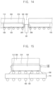
- FIGS. 11 , 12 , 13 , 14 and 15 are related cross-sectional views illustrating in one example a method of manufacture for the semiconductor package of FIG. 8 ;
- FIG. 16 is a cross-sectional view illustrating a semiconductor package according to embodiments of the inventive concept.
- FIG. 17 is an enlarged, cross-sectional view of portion “E” in FIG. 16 ;
- FIG. 18 is a cross-sectional view taken along line F-F′ in FIG. 16 ;
- FIGS. 19 , 20 , 21 , 22 and 23 are related cross-sectional views illustrating in one example a method of manufacture for the semiconductor package of FIG. 16 .
- Geometric terms may include, for example: height/width; vertical/horizontal; top/bottom; higher/lower; closer/farther; thicker/thinner; proximate/distant; above/below; under/over; upper/lower; center/side; surrounding; overlay/underlay; etc.
- FIG. 1 is a cross-sectional view illustrating a semiconductor package 100 according to embodiments of the inventive concept.
- FIG. 2 is an enlarged, cross-sectional view illustrating portion “A” in FIG. 1
- FIG. 3 is a cross-sectional view taken along line B-B′ in FIG. 1 .
- the semiconductor package 100 may include a package substrate 110 , a semiconductor chip 120 , conductive bumps 130 , a molding member 140 , an underfilling layer 150 and external terminals 160 .
- the package substrate 110 may include an insulation substrate and a conductive pattern, wherein the conductive pattern may be arranged upon and/or within the insulation substrate.
- the conductive pattern may include an upper conductive pattern associated with (e.g., disposed on and/or exposed by) an upper surface of the package substrate 110 , and/or a lower conductive pattern associated with a lower surface of the package substrate 110 .
- the semiconductor chip 120 may be disposed (e.g., arranged over and/or mounted on) the upper (or active) surface of the package substrate 110 .
- Electrically conductive pads 112 may be arranged on a lower surface of the semiconductor chip 120 to face the upper surface of the package substrate 110 when the semiconductor chip 120 is disposed on the package substrate 110 .
- the principal upper/lower surfaces of the package substrate 110 may be understood as being laterally (or horizontally) oriented according to a first horizontal direction and a second horizontal directions (e.g., an X direction and a Y direction).
- the semiconductor chip 120 may be understood as being vertically disposed on the package substrate 110 according to a vertical direction (e.g., a Z direction) substantially orthogonal to the first and second horizontal directions.
- the conductive bumps 130 may be respectively disposed on the lower surface of the semiconductor 120 (e.g., on or over the pads 112 ), such that the conductive bumps 120 are interposed between the package substrate 110 and the semiconductor chip 120 . At least some of the conductive bumps 130 may be configured to electrically connect the upper conductive pattern of the package substrate 110 with the pads 112 . Thus, in operational effect, various conductive pattern(s) and circuitry of the semiconductor chip 120 may be electrically connected with the upper conductive pattern of the package substrate 110 via the conductive bumps 130 .
- the underfilling layer 150 may be interposed between the package substrate 110 and the semiconductor chip 120 .
- the underfilling layer 150 may substantially surround the respective conductive bumps 130 .
- the external terminals 160 may be disposed on the lower surface of the package substrate 110 in electrical contact with the lower conductive pattern disposed on the lower surface of the package substrate 110 .
- the molding member 140 may mold around (wholly or in part) the side surface(s) of the semiconductor chip 120 .
- the molding member 140 (e.g., an epoxy molding compound or EMC) may be molded around to substantially surround the side surfaces of the semiconductor chip 120 . In some embodiments, the molding member 140 may not cover any portion of the upper surface of the semiconductor chip 120 , but in other embodiments, the molding member 140 may cover some or all of the upper surface of the semiconductor chip 120 .
- the molding member 140 may include a protruding sidewall portion that extends horizontally and outwardly (hereafter, the protruding sidewall 170 ).
- the term “outwardly” denotes a direction away from a vertical center axis of the semiconductor package.
- the protruding sidewall 170 may be a materially integral part (or portion) of the molding member 140 produced by a conventionally understood a molding process. Once formed (as described in detail hereafter) the protruding sidewall may include an upper portion above the protruding sidewall 170 and a lower portion below the protruding sidewall portion.
- Each of the upper portion of the molding member 140 , the lower portion of the molding member 140 and the protruding sidewall portion of the molding member 140 may have a corresponding width measured in a same horizontal direction from (e.g.,) a proximate vertical sidewall of a semiconductor device.
- the protruding sidewall 170 may be understood as horizontally protruding (or extending) farther from the center axis of the semiconductor package than at least one of the upper portion of the molding member 140 and the lower portion of the molding member 140 .
- the protruding sidewall 170 of the molding member 140 may be further understood as having an upper end 172 , a lower end 174 and an outer side surface 176 .
- the upper end 172 and the lower end 174 may each outwardly and horizontally extend away from the from the semiconductor chip 120 .
- the outer side surface 176 of the protruding sidewall of the molding member 140 may extend between the upper end 172 and the lower end 174 .
- the outer side surface 176 may form a substantially vertical surface.
- the molding member 140 including the protruding sidewall 170 may substantially surround all of the side surfaces of the semiconductor chip 120 . (This feature is illustrated in FIG. 3 ). Accordingly, the molding member 140 including the protruding sidewall 170 may have a rectangular frame shape substantially surrounding the semiconductor chip 120 .
- the upper end 172 of the protruding sidewall 170 may be vertically offset below an upper surface of the molding member 140 (which may, in some embodiments, be coplanar with the upper surface of the semiconductor chip 120 ).
- the vertical offset distance (L 1 ) between the upper surface of the molding member 140 and the upper end 172 of the protruding sidewall 170 will be at least about 20 ⁇ m, however the scope of the inventive concept is not limited thereto.
- the lower end 174 of the protruding sidewall 170 horizontally and outwardly extends away from the semiconductor chip 120 at a first vertical height substantially coplanar with (or defined by) a lower surface of the molding member 140 which is coplanar with the lower surface of the semiconductor chip 120 .
- FIGS. 4 to 7 are related cross-sectional views illustrating in one example a method of manufacture for the semiconductor package of FIG. 1 .
- the molding member 140 may be molded around (wholly or in part) multiple semiconductor chips 120 .
- the molding member 140 may be formed between the side surfaces of respectively adjacent semiconductor chips 120 . In this manner, the molding member 140 may substantially surround at least the side surfaces of the semiconductor chips 120 .
- a molding process used to mold the molding ember 140 around the semiconductor chips 120 may be performed as part of mechanically supporting the semiconductor chips 120 during fabrication using a supporting substrate. After the molding process forming the molding member 140 is complete, the supporting substrate may be removed from the semiconductor chips 120 . Then, the conductive bumps 130 may be arranged on the lower surface of each of the semiconductor chips 120 . Alternately, the molding process forming the molding member 140 may be performed after arranging the conductive bumps 130 on the lower surface of the semiconductor chips 120 .
- a carrier substrate 200 may be attached to the upper surfaces of the semiconductor chips 120 using an adhesive 210 . With this configuration, the semiconductor chips 120 may be supported by the carrier substrate 200 .
- many conventionally available carrier substrates may include one or more materials such as glass, epoxy, a semiconductor material, etc.
- selected portions of the carrier substrate 200 may be removed (or cut away) using a first blade B 1 .
- the selected portions of the carrier substrate 200 removed by application of the first blade B 1 may be portions of the carrier substrate 200 respectively overlaying portions of the molding member 140 disposed between adjacent ones of the semiconductor chips 120 .
- the first blade B 1 may penetrate from an upper surface of the carrier substrate 200 to a lower surface of the adhesive 210 , thereby forming a vertically-aligned first cutting groove 202 through the carrier substrate 200 and the adhesive 210 .
- the first blade B 1 may be selected (e.g., from a variety of conventionally available saw blades) according to cutting characteristics optimally applied to the cutting of the glass substrate.
- the generation of an edge burr or other damage to the glass substrate may be minimized or prevented by use of an appropriate blade selected as the first blade B 1 in relation to the constituent material(s) of the carrier substrate 200 .
- the first blade B 1 may partially penetrate into the upper surface of the molding member 140 .
- stopping the descending first blade B 1 before fully removing the adhesive 210 underlaying the selected portions of the carrier substrate 200 may result in adhesive residue adhering to, and possibly clogging the first blade B 1 .
- a first cutting process performed with the first blade B 1 should not be stopped part-way through the adhesive 210 .
- a first width of the first cutting groove 202 may be particularly defined by appropriate selection of the first blade B 1 having a first blade-width substantially equal to the desired first width.
- a second cutting process using a second blade B 2 may be applied to selected portions of the molding member 140 between adjacent ones of the semiconductor chips 120 .
- the second blade B 2 may be selected according to optimal cutting characteristics relative to the material(s) forming the molding member 140 , and may be characterized by a second blade-width, different from (e.g., more narrow than) the first blade-width.
- the second blade B 2 may pass through the thickness of the molding member 140 to form a vertically-aligned, second cutting groove 204 .
- the second cutting groove 204 will be narrower than the first cutting groove 202 .
- the molding member 140 including the protruding sidewall 170 and described above in relation to FIGS. 1 , 2 and 3 may be formed.
- the second cutting groove 204 may pass into the first cutting groove 202 to effectively divide adjacent semiconductor chips 120 one from the other. Yet, the divided semiconductor chips 120 remain well supported by the carrier substrate 200 . Alternately, the second cutting process using the second blade B 2 may be performed before the first cutting process using the first blade B 1 .
- the semiconductor chip 120 still supported by the carrier substrate 200 , may be flipped and mounted (e.g., bonded) to the package substrate 110 via the conductive bumps 130 . That is, once the supported semiconductor chip 120 is flipped, the conductive bumps 130 —now on the lower surface of the semiconductor chip 120 —may be electrically connected to the upper conductive pattern on the upper surface of the package substrate 110 .
- a reflow process may be applied to electrically connect the conductive bumps 130 to the upper conductive pattern on the upper surface of the package substrate 110 .
- the semiconductor chip 120 may be compressed to (e.g., mounted on) the package substrate 110 .
- the carrier substrate 200 supporting the semiconductor chip 120 has the effect of suppressing or preventing warpage of the semiconductor chip 120 .
- the risk of warpage in the semiconductor chip 120 may be prospectively guarded against by appropriately selecting a thickness of the carrier substrate 200 and/or a thickness of the adhesive 210 .
- the carrier substrate 200 may be detached from the semiconductor chip 120 to complete the semiconductor package 100 of FIG. 1 .
- a laser may be selective applied to the adhesive 210 in order to weaken its adhesive strength. Once the adhesive strength of the adhesive 210 has been sufficiently weakened, the carrier substrate 200 may be readily detached from the semiconductor chip 120 without risk of damage to the semiconductor chip 120 .
- FIG. 8 is a cross-sectional view illustrating a semiconductor package 100 a in accordance with embodiments of the inventive concept.
- FIG. 9 is an enlarged, cross-sectional view of portion “C” in FIG. 8
- FIG. 10 is a cross-sectional view taken along line D-D′ in FIG. 8 .
- the semiconductor package 100 a of FIG. 8 may include substantially the same elements as those described in relation to the semiconductor package 100 of FIG. 1 , except that the shape of the protruding sidewall is different.
- the molding member 140 includes a protruding sidewall 180 having an upper end 182 , a lower end 184 and an outer side surface 186 .
- the upper end 182 of the protruding sidewall 180 is substantially the same as the upper end 172 of the protruding sidewall 170 described in relation to FIGS. 1 , 2 and 3 .
- the lower end 184 of the protrusion 180 horizontally and outwardly extends away from the semiconductor chip 120 at a second vertical height well above the first vertical height associated with plane defined by the lower surface 174 of the molding member 140 and the lower surface of the semiconductor chip 120 .
- the vertical length of the outer side surface 186 of the protruding sidewall 180 is substantially shorter than the outer side surface 176 of the protruding sidewall 170 .
- the upper end 182 of the protruding sidewall 180 may again vertically offset by the distance L 1 (e.g., at least about 20 ⁇ m) from the upper surface of the molding member 140 .
- the lower end 184 of the protruding sidewall 180 may be further vertically offset above the lower surface 174 of the molding member 140 by a distance L 2 .
- the second distance L 2 may also be at least about 20 ⁇ m, but the scope of the inventive concept is not limited thereto.
- the degree of horizontal and outward extension by the upper end 182 of the protruding sidewall 180 may be different from (e.g., greater than) the degree of horizontal and outward extension of the lower end 184 of the protruding sidewall 180 .
- FIGS. 11 to 15 are related cross-sectional vies illustrating in one example a method of manufacture for the semiconductor package of FIG. 8 .
- the molding member 140 is molded (wholly or in part) around multiple semiconductor chips 120 , and the conductive bumps 130 may be arranged on the lower surface of each of the semiconductor chips 120 .
- a carrier substrate 200 is again attached to the upper surfaces of the semiconductor chips 120 using the adhesive 210 in order to support the semiconductor chips 120 .
- selected portions of the carrier substrate 200 (along with corresponding portions of the adhesive 210 ) overlaying portions of the molding member 140 between adjacent ones of the semiconductor chips 120 are removed (e.g., cut away) using the first blade B 1 .
- the first blade B 1 is allowed to slightly penetrate into the upper surface of the molding member 140 to fully and cleanly remove portions of the adhesive 210 underlying the selected portions of the carrier substrate 200 .
- the second blade B 2 is similarly applied to portions of the molding member 140 between adjacent ones of the semiconductor chips 120 , as described in relation to FIG. 6 —however the second cutting process performed by the second blade B 2 does not completely penetrate the molding member 140 .
- the second blade B 2 may have the second blade-width narrower than the first blade-width of the first blade B 1 , thus yielding the second cutting groove 204 having a second width narrower than a first width of the first cutting groove 202 formed by the first blade B 1 .
- a third blade B 3 may be applied to a remaining portion of the molding member 140 in second cutting groove 204 between the adjacent ones of the semiconductor chips 120 to form a third cutting groove 206 .
- the combination of the first cutting groove 202 , the second cutting groove 204 and finally, the third cutting groove 206 effectively divides the adjacent the semiconductor chips 120 one from the other. However, the divided semiconductor chips 120 remain supported by portions of the carrier substrate 200 .
- the third blade B 3 may have a third blade-width narrower than the second blade-width of the second blade B 2 . Accordingly, the third cutting groove 206 formed by the third blade B 3 will be narrower than the second cutting groove 204 . As a result, the protruding sidewall 180 may be formed having the shape described in relation to FIGS. 8 , 9 and 10 .
- the first cutting process using the first blade B 1 may be performed.
- the semiconductor chip 120 supported by the carrier substrate 200 may be bonded to the package substrate 110 via the conductive bumps 130 as previously described in relation to FIG. 7 .
- FIG. 16 is a cross-sectional view illustrating a semiconductor package 300 according to embodiments of the inventive concept.
- FIG. 17 is an enlarged cross-sectional view of portion “E” in FIG. 16
- FIG. 18 is a cross-sectional view taken along line F-F′ in FIG. 16 .
- the semiconductor package 300 may be a 2.5D stack type semiconductor package that includes a package substrate 310 , an interposer 320 , at least one first semiconductor chip 330 , a plurality of second semiconductor chips 340 , a molding member 360 and external terminals 370 .
- the interposer 320 may be disposed on an upper surface of the package substrate 310 , and be electrically connected with the package substrate 310 via conductive bumps 350 .
- Connection vias 322 may be vertically arranged in relation to the interposer 320 , wherein upper ends of the connection vias 322 are exposed through an upper surface of the interposer 320 and lower ends of the connection vias 322 may be exposed through a lower surface of the interposer 320 .
- the first semiconductor chip 330 may be arranged on the upper surface of the interposer 320 .
- the first semiconductor chip 330 may be electrically connected with the interposer 320 via first conductive bumps 352 . That is, the first semiconductor chip 330 may be electrically connected with the upper ends of the connection vias 322 via the first conductive bumps 352 .
- the first semiconductor chip 330 may be a central processing unit (CPU), a graphic processing unit (GPU), etc.
- the plurality of second semiconductor chips 340 may be vertically stacked on the upper surface of the interposer 320 . In some embodiments, separate stacked pluralities of the second semiconductor chips 340 may be arranged on opposing sides of the first semiconductor chip 330 .
- the embodiment of FIG. 16 includes a first stacked plurality of second semiconductor chips 340 and a second stacked plurality of second semiconductor chips, as one illustrative example.
- each stacked plurality of second semiconductor chips 340 may be electrically connected with the interposer 320 via second conductive bumps 354 . That is, each stacked plurality of second semiconductor chips 340 may be electrically connected with the upper ends of the connection vias 322 via the second conductive bumps 354 .
- the second semiconductor chips 340 may be high-bandwidth memory (HBM) chips, for example.
- HBM high-bandwidth memory
- An underfilling layer 390 may be interposed between the package substrate 110 and the interposer 320 .
- the underfilling layer 390 may be configured to substantially surround each of the lower conductive bumps 350 between the package substrate 310 and the interposer 320 .
- the external terminals 370 may be mounted on the lower surface of the package substrate 310 .
- the external terminals 370 may electrically contact with lower ends of the conductive patterns exposed through a lower surface of the package substrate 310 .
- the molding member 360 (e.g., an epoxy molding compound or EMC) may be disposed on the upper surface of the interposer 320 and may be molded around and in between the first semiconductor chip 330 , the first stacked plurality of second semiconductor chips 340 and the second stacked plurality of second semiconductor chips 340 .
- the molding member 360 may be interposed between the first semiconductor chip 330 and each one of the stacked pluralities of second semiconductor chips 340 , as illustrated in FIG. 18 .
- the molding member 360 of FIGS. 16 , 17 and 18 includes a protruding sidewall 380 .
- the protruding sidewall 380 may include an upper end 382 , a lower end 384 and an outer side surface 386 .
- the upper end 382 of the protruding sidewall 380 may horizontally extend outwardly away from the first semiconductor chip 330 .
- the lower end 384 of the protruding sidewall 380 may also horizontally extend outwardly away from the first semiconductor chip 330 .
- the outer side surface 386 of the protruding sidewall 380 may vertically extend between the upper ends 382 of the protruding sidewall 380 with the lower end 384 of the protruding sidewall 380 .
- the upper end 382 of the protruding sidewall 380 may be vertically offset below the upper surface of the molding member 360 by a first distance L 31 (e.g., at least about 20 ⁇ m). Further, the lower end 384 of the protruding sidewall 380 may be vertically offset above the lower surface of the molding member 360 by a second distance L 32 (e.g., at least about 20 ⁇ m).
- a vertical height (T) of the outer side surface 386 may be determined in accordance with the first distance L 31 between the upper surface of the molding member 360 and the upper end 382 of the protruding sidewall 380 and the second distance L 32 between the lower surface of the molding member 360 and the lower end 384 of the protruding sidewall 380 .
- an upper protruding width (measured in a horizontal direction) of the upper end 382 in the protruding sidewall 380 may be different (e.g., greater than) a lower protruding width (measured in the same horizontal direction) of the lower end 384 in the protruding sidewall 380 .
- FIGS. 19 to 23 are related cross-sectional views illustrating in one example a method of manufacture for the semiconductor package of FIG. 16 .
- the first semiconductor chip 330 and the stacked pluralities of second semiconductor chips 340 may be arranged on the upper surface of the interposer 320 . That is, the first semiconductor chip 330 and the stacked pluralities of second semiconductor chips 340 may be arranged in respective package regions on the upper surface of the interposer 320 . In these package regions, for example, stacked pluralities of second semiconductor chips 340 may be disposed on opposing sides of the first semiconductor chip 330 .
- the lower conductive bumps 350 may be arranged on the lower surface of the interposer 320 .
- the molding member 360 may molded around the first semiconductor chip 330 and the stacked pluralities of second semiconductor chips 340 .
- a carrier substrate 200 may be attached to the upper surfaces of the first and second semiconductor chips 330 and 340 and the upper surface of the molding member 360 using an adhesive 210 .
- the interposer 320 and the first and second semiconductor chips 330 and 340 may be supported by the carrier substrate 200 .
- selected portions of the carrier substrate 200 along with underlying portions of the adhesive 210 disposed over portions of the molding member 360 between the second semiconductor chips 340 may be removed (e.g., cut away) using the first blade B 1 .
- the first blade B 1 may be selected and used in a manner similar to that previously described in relation to FIG. 12 to form a first cutting groove 202 .
- the second blade B 2 may be selected and used to cut through the interposer 320 and a selected portion of the molding member 360 between adjacent, stacked pluralities of second semiconductor chips 340 .
- the second blade B 2 may have a second blade-width narrower than a first blade-width of the first blade B 1 .
- the second blade B 2 may penetrate completely through the interposer 320 and partially through the molding member 140 to form a second cutting groove 204 .
- the interposer 320 may include different material(s) than those used in the molding member 360 .
- a summed vertical thicknesses of the interposer 320 and the molding member 360 may be relatively thicker than the material layer thicknesses previously implicated in the previous embodiments. Accordingly, the combination of the interposer 320 and at least part of the molding member 360 may not be readily cut using the second blade B 2 .
- the third blade B 3 may be used to cut a remaining portion of the molding member 360 between the adjacent stacked pluralities of the second semiconductor chips 340 in order to completely form the third cutting groove 206 .
- the combination of the first cutting groove 202 , the second cutting groove 204 and the third cutting groove 206 may be used to divide adjacent stacked pluralities of second semiconductor chips 340 one from the other.
- multiple package structures may be obtained, each including a cut portion of the interposer 320 , the first semiconductor chip 330 and at least one stacked plurality of second semiconductor chips 340 .
- each one of the resulting package structures will be supported by the carrier substrate 200 .
- the third blade B 3 may have a third blade-width narrower than the second blade-width of the second blade B 2 .
- the third cutting groove 206 formed by the third blade B 3 may be narrower than the second cutting groove 204 .
- the molding member 360 surrounding the combination of the first semiconductor chip 330 and at least one stacked plurality of second semiconductor chips 340 will include the protruding sidewall 380 having the shape described above and illustrated (e.g.,) in FIG. 17 .
- the first cutting process using the first blade B 1 may be performed.
- the package structure supported by the carrier substrate 200 may be bonded to the package substrate 310 via the conductive bumps 350 .
- the lower conductive bumps 350 on the lower surface of the interposer 320 may be arranged on the upper surface of the package substrate 310 .
- a reflow process may be performed on the conductive bumps 350 , and simultaneously, the interposer 320 may be compressed to the package substrate 310 .
- embodiments of the inventive concept use a cut portion of the carrier substrate 200 to support the interposer 320 , thereby suppressing warpage. Additionally, the risk of warpage associated with the interposer 320 may be controlled by appropriately selecting a thickness of the carrier substrate 200 and/or a thickness of the adhesive 210 .
- the underfilling layer 390 may be formed between the interposer 320 and the package substrate 310 to surround the lower conductive bumps 350 with the underfilling layer 390 .
- the external terminals 370 may be mounted on the lower surface of the package substrate 310 .
- the carrier substrate 200 may then be detached, as previously described, from the package structure to complete the semiconductor package 300 in FIG. 17 .
- a carrier substrate may be attached to an upper surface of the semiconductor chip or an upper surface of the semiconductor chip over an interposer using adhesive.
- warpage of the semiconductor chip and/or the interposer may be controlled by appropriately selecting a thickness of the carrier substrate and/or a thickness of the adhesive.
Landscapes
- Engineering & Computer Science (AREA)
- Microelectronics & Electronic Packaging (AREA)
- Power Engineering (AREA)
- Computer Hardware Design (AREA)
- Physics & Mathematics (AREA)
- Condensed Matter Physics & Semiconductors (AREA)
- General Physics & Mathematics (AREA)
- Manufacturing & Machinery (AREA)
- Structures Or Materials For Encapsulating Or Coating Semiconductor Devices Or Solid State Devices (AREA)
- Dicing (AREA)
- Wire Bonding (AREA)
Abstract
A method of manufacture for a semiconductor package includes; forming a molding member on side surfaces of the semiconductor chips, using an adhesive to attach a carrier substrate to upper surfaces of the molding member and the semiconductor chips, using a first blade having a first blade-width to cut away selected portions of the carrier substrate and portions of the adhesive underlying the selected portions of the carrier substrate, and using the first blade to partially cut into an upper surface of the molding member to form a first cutting groove, wherein the selected portions of the carrier substrate are dispose above portions of the molding member between adjacent ones of semiconductor chips, using a second blade having a second blade-width narrower than the first blade-width to cut through a lower surface of the molding member to form a second cutting groove, wherein a combination of the first cutting groove and the second cutting groove separate a package structure including a semiconductor chip supported by a cut portion of the carrier substrate and bonding the package structure to an upper surface of a package substrate.
Description
This is a Continuation of U.S. application Ser. No. 17/177,725, filed Feb. 17, 2021, and a claim of priority is made to Korean Patent Application No. 10-2020-0113839 filed on Sep. 7, 2020, in the Korean Intellectual Property Office (KIPO), the subject matter of which is hereby incorporated by reference.
Embodiments of the inventive concept relate generally to semiconductor packages and methods for manufacturing the same. More particularly, embodiments of the inventive concept relate to flip-chip type semiconductor packages and methods for manufacturing the same.
Flip-chip type semiconductor packages generally include a package substrate, a semiconductor chip, and conductive bumps interposed between the package substrate and the semiconductor chip. The conductive bumps may be used to electrically connect the semiconductor chip with a conductive on the package substrate using a reflow process.
However, the semiconductor chip and the package substrate may be constructed of various and different materials having different coefficients of thermal expansion. Accordingly, there is some risk that thermal stress applied to the semiconductor chip, an interposer and/or the package substrate may cause material(s) warpage.
Embodiments of the inventive concept provide semiconductor packages more resistant to thermal stress potentially causing material(s) warpage. Embodiments of the inventive concept also provide methods of manufacture for such semiconductor packages.
In some embodiments, a semiconductor package may include; a package substrate, an interposer disposed on an upper surface of the package substrate, a first semiconductor chip and a stacked plurality of second semiconductor chips disposed on an upper surface of the interposer, and a molding member around side surfaces of the first semiconductor chip and the stacked plurality of second semiconductor chips. Here, the molding member may include a protruding sidewall including an upper end that extends horizontally outward and is vertically offset below an upper surface of the molding member by a first distance, a lower end that extends horizontally outward and is vertically offset above a lower surface of the molding member by a second distance, and an outer side surface vertically extending between the upper end and the lower end, wherein an upper protruding width of the upper end is greater than a lower protruding width of the lower end.
In some embodiments, a semiconductor package may include; a package substrate, an interposer disposed on an upper surface of the package substrate, a first semiconductor chip disposed on an upper surface of the interposer, a second semiconductor chip disposed on the upper surface of the interposer; and a molding member includes an upper surface, an upper portion, a lower portion and a protruding sidewall, wherein the molding member is molded around side surfaces of the first semiconductor chip and the second semiconductor chip. The protruding sidewall may include an upper end vertically offset below the upper surface of the molding member, and have a width greater than a width of the upper portion of the molding member.
In some embodiments, a method of manufacture for a semiconductor package may include; arranging a first semiconductor chip, a first stacked plurality of second semiconductor chips and a second stacked plurality of second semiconductor chips on an upper surface of an interposer, forming a molding member on side surfaces of the first semiconductor chips, the first stacked plurality of second semiconductor chips and the second stacked plurality of second semiconductor chips, using an adhesive to attach a carrier substrate to an upper surface of the molding member, an upper surface of the first semiconductor chip, an upper surface of the first stacked plurality of second semiconductor chips and an upper surface of the second stacked plurality of second semiconductor chips, using a first blade having a first blade-width to cut away selected portions of the carrier substrate and cut away portions of the adhesive underlying the selected portions of the carrier substrate, and using the first blade to partially cut into an upper surface of the molding member to form a first cutting groove, wherein the selected portions of the carrier substrate are dispose above portions of the molding member between the first stacked plurality of second semiconductor chips and the second stacked plurality of second semiconductor chips, using a second blade having a second blade-width narrower than the first blade-width to cut through the interposer and at least partially into a lower surface of the molding member to form a second cutting groove, wherein a combination of the first cutting groove and the second cutting groove separate a package structure including a cut portion of the interposer, the first semiconductor chip and the first stacked plurality of second semiconductor chips, collectively supported by a cut portion of the carrier substrate and bonding the package structure to an upper surface of a package substrate.
In some embodiments, a method of manufacture for a semiconductor package may include; forming a molding member on side surfaces of the semiconductor chips, using an adhesive to attach a carrier substrate to upper surfaces of the molding member and the semiconductor chips, using a first blade having a first blade-width to cut away selected portions of the carrier substrate and portions of the adhesive underlying the selected portions of the carrier substrate, and using the first blade to partially cut into an upper surface of the molding member to form a first cutting groove, wherein the selected portions of the carrier substrate are dispose above portions of the molding member between adjacent ones of semiconductor chips, using a second blade having a second blade-width narrower than the first blade-width to cut through a lower surface of the molding member to form a second cutting groove, wherein a combination of the first cutting groove and the second cutting groove separate a package structure including a semiconductor chip supported by a cut portion of the carrier substrate, and bonding the package structure to an upper surface of a package substrate.
The inventive concept may be more clearly understood upon consideration of certain embodiments illustrated in the accompanying drawings, in which:
Throughout the written description and drawings, like reference numbers and labels are used to denote like or similar elements, components, steps and/or features. Throughout the written description, certain geometric terms may be used to highlight relative relationships between elements, components and/or features with respect to certain embodiments of the inventive concept. Those skilled in the art will recognize that such geometric terms are relative in nature, arbitrary in descriptive relationship(s) and/or directed to aspect(s) of the illustrated embodiments. Geometric terms may include, for example: height/width; vertical/horizontal; top/bottom; higher/lower; closer/farther; thicker/thinner; proximate/distant; above/below; under/over; upper/lower; center/side; surrounding; overlay/underlay; etc.
Figure (FIG. 1 is a cross-sectional view illustrating a semiconductor package 100 according to embodiments of the inventive concept. FIG. 2 is an enlarged, cross-sectional view illustrating portion “A” in FIG. 1 , and FIG. 3 is a cross-sectional view taken along line B-B′ in FIG. 1 .
Referring to FIGS. 1, 2 and 3 , the semiconductor package 100 may include a package substrate 110, a semiconductor chip 120, conductive bumps 130, a molding member 140, an underfilling layer 150 and external terminals 160.
The package substrate 110 may include an insulation substrate and a conductive pattern, wherein the conductive pattern may be arranged upon and/or within the insulation substrate. Here, the conductive pattern may include an upper conductive pattern associated with (e.g., disposed on and/or exposed by) an upper surface of the package substrate 110, and/or a lower conductive pattern associated with a lower surface of the package substrate 110.
The semiconductor chip 120 may be disposed (e.g., arranged over and/or mounted on) the upper (or active) surface of the package substrate 110. Electrically conductive pads 112 may be arranged on a lower surface of the semiconductor chip 120 to face the upper surface of the package substrate 110 when the semiconductor chip 120 is disposed on the package substrate 110.
With the exemplary configuration of FIG. 1 in mind, the principal upper/lower surfaces of the package substrate 110, as well as the principal upper/lower surfaces of the semiconductor chip 120, may be understood as being laterally (or horizontally) oriented according to a first horizontal direction and a second horizontal directions (e.g., an X direction and a Y direction). Hence, the semiconductor chip 120 may be understood as being vertically disposed on the package substrate 110 according to a vertical direction (e.g., a Z direction) substantially orthogonal to the first and second horizontal directions.
The conductive bumps 130 may be respectively disposed on the lower surface of the semiconductor 120 (e.g., on or over the pads 112), such that the conductive bumps 120 are interposed between the package substrate 110 and the semiconductor chip 120. At least some of the conductive bumps 130 may be configured to electrically connect the upper conductive pattern of the package substrate 110 with the pads 112. Thus, in operational effect, various conductive pattern(s) and circuitry of the semiconductor chip 120 may be electrically connected with the upper conductive pattern of the package substrate 110 via the conductive bumps 130.
The underfilling layer 150 may be interposed between the package substrate 110 and the semiconductor chip 120. Here, the underfilling layer 150 may substantially surround the respective conductive bumps 130.
The external terminals 160 (e.g., solder balls or similar conductive elements) may be disposed on the lower surface of the package substrate 110 in electrical contact with the lower conductive pattern disposed on the lower surface of the package substrate 110.
The molding member 140 may mold around (wholly or in part) the side surface(s) of the semiconductor chip 120.
In some embodiments, the molding member 140 (e.g., an epoxy molding compound or EMC) may be molded around to substantially surround the side surfaces of the semiconductor chip 120. In some embodiments, the molding member 140 may not cover any portion of the upper surface of the semiconductor chip 120, but in other embodiments, the molding member 140 may cover some or all of the upper surface of the semiconductor chip 120.
According to certain embodiments of the inventive concept, the molding member 140 may include a protruding sidewall portion that extends horizontally and outwardly (hereafter, the protruding sidewall 170). In this context, the term “outwardly” denotes a direction away from a vertical center axis of the semiconductor package. Here, the protruding sidewall 170 may be a materially integral part (or portion) of the molding member 140 produced by a conventionally understood a molding process. Once formed (as described in detail hereafter) the protruding sidewall may include an upper portion above the protruding sidewall 170 and a lower portion below the protruding sidewall portion. Each of the upper portion of the molding member 140, the lower portion of the molding member 140 and the protruding sidewall portion of the molding member 140 may have a corresponding width measured in a same horizontal direction from (e.g.,) a proximate vertical sidewall of a semiconductor device. Thus, the protruding sidewall 170 may be understood as horizontally protruding (or extending) farther from the center axis of the semiconductor package than at least one of the upper portion of the molding member 140 and the lower portion of the molding member 140.
The protruding sidewall 170 of the molding member 140 may be further understood as having an upper end 172, a lower end 174 and an outer side surface 176. Here, the upper end 172 and the lower end 174 may each outwardly and horizontally extend away from the from the semiconductor chip 120. The outer side surface 176 of the protruding sidewall of the molding member 140 may extend between the upper end 172 and the lower end 174. Thus, the outer side surface 176 may form a substantially vertical surface.
In some embodiments of the inventive concept, the molding member 140 including the protruding sidewall 170 may substantially surround all of the side surfaces of the semiconductor chip 120. (This feature is illustrated in FIG. 3 ). Accordingly, the molding member 140 including the protruding sidewall 170 may have a rectangular frame shape substantially surrounding the semiconductor chip 120.
As illustrated in FIG. 2 , the upper end 172 of the protruding sidewall 170 may be vertically offset below an upper surface of the molding member 140 (which may, in some embodiments, be coplanar with the upper surface of the semiconductor chip 120). In some embodiments, the vertical offset distance (L1) between the upper surface of the molding member 140 and the upper end 172 of the protruding sidewall 170 will be at least about 20 μm, however the scope of the inventive concept is not limited thereto.
Here, the lower end 174 of the protruding sidewall 170 horizontally and outwardly extends away from the semiconductor chip 120 at a first vertical height substantially coplanar with (or defined by) a lower surface of the molding member 140 which is coplanar with the lower surface of the semiconductor chip 120.
Referring to FIG. 4 , the molding member 140 may be molded around (wholly or in part) multiple semiconductor chips 120. In particularly, the molding member 140 may be formed between the side surfaces of respectively adjacent semiconductor chips 120. In this manner, the molding member 140 may substantially surround at least the side surfaces of the semiconductor chips 120.
In this regard, a molding process used to mold the molding ember 140 around the semiconductor chips 120 may be performed as part of mechanically supporting the semiconductor chips 120 during fabrication using a supporting substrate. After the molding process forming the molding member 140 is complete, the supporting substrate may be removed from the semiconductor chips 120. Then, the conductive bumps 130 may be arranged on the lower surface of each of the semiconductor chips 120. Alternately, the molding process forming the molding member 140 may be performed after arranging the conductive bumps 130 on the lower surface of the semiconductor chips 120.
As illustrated in FIG. 4 , a carrier substrate 200 may be attached to the upper surfaces of the semiconductor chips 120 using an adhesive 210. With this configuration, the semiconductor chips 120 may be supported by the carrier substrate 200. Here, it should be noted that many conventionally available carrier substrates may include one or more materials such as glass, epoxy, a semiconductor material, etc.
Referring to FIG. 5 , selected portions of the carrier substrate 200, along with portions of the adhesive 210 underlying these selected portions of the carrier substrate 200) may be removed (or cut away) using a first blade B1. Here, the selected portions of the carrier substrate 200 removed by application of the first blade B1 may be portions of the carrier substrate 200 respectively overlaying portions of the molding member 140 disposed between adjacent ones of the semiconductor chips 120.
In this regard, the first blade B1 may penetrate from an upper surface of the carrier substrate 200 to a lower surface of the adhesive 210, thereby forming a vertically-aligned first cutting groove 202 through the carrier substrate 200 and the adhesive 210. When the carrier substrate 200 is a glass substrate, for example, the first blade B1 may be selected (e.g., from a variety of conventionally available saw blades) according to cutting characteristics optimally applied to the cutting of the glass substrate. In this regard, the generation of an edge burr or other damage to the glass substrate may be minimized or prevented by use of an appropriate blade selected as the first blade B1 in relation to the constituent material(s) of the carrier substrate 200.
According to certain embodiments of the inventive concept, during application of the first blade B1 to fully remove the selected portions of the carrier substrate 200 and the corresponding portions of the adhesive 210, the first blade B1 may partially penetrate into the upper surface of the molding member 140. Here, it should be noted that stopping the descending first blade B1 before fully removing the adhesive 210 underlaying the selected portions of the carrier substrate 200 may result in adhesive residue adhering to, and possibly clogging the first blade B1. In order to prevent clogging, a first cutting process performed with the first blade B1 should not be stopped part-way through the adhesive 210. Thus, by allowing the first blade B1 to partially penetrate into the upper surface of the molding member 140, the selected portions of the carrier substrate 200 along with corresponding portions of the adhesive 210 may be fully and cleanly removed. As a result of this approach, a first width of the first cutting groove 202 may be particularly defined by appropriate selection of the first blade B1 having a first blade-width substantially equal to the desired first width.
Referring to FIG. 6 , a second cutting process using a second blade B2 may be applied to selected portions of the molding member 140 between adjacent ones of the semiconductor chips 120. Here, the second blade B2 may be selected according to optimal cutting characteristics relative to the material(s) forming the molding member 140, and may be characterized by a second blade-width, different from (e.g., more narrow than) the first blade-width.
In its operational application, the second blade B2 may pass through the thickness of the molding member 140 to form a vertically-aligned, second cutting groove 204. Here, in some embodiments, because the second blade-width of the second blade B2 is narrower than the first blade-width of the first blade B1, the second cutting groove 204 will be narrower than the first cutting groove 202. Using this dual cutting approach as one example, the molding member 140 including the protruding sidewall 170 and described above in relation to FIGS. 1, 2 and 3 may be formed.
Thus, the second cutting groove 204 may pass into the first cutting groove 202 to effectively divide adjacent semiconductor chips 120 one from the other. Yet, the divided semiconductor chips 120 remain well supported by the carrier substrate 200. Alternately, the second cutting process using the second blade B2 may be performed before the first cutting process using the first blade B1.
Referring to FIG. 7 , the semiconductor chip 120 still supported by the carrier substrate 200, may be flipped and mounted (e.g., bonded) to the package substrate 110 via the conductive bumps 130. That is, once the supported semiconductor chip 120 is flipped, the conductive bumps 130—now on the lower surface of the semiconductor chip 120—may be electrically connected to the upper conductive pattern on the upper surface of the package substrate 110. In this regard, for example, a reflow process may be applied to electrically connect the conductive bumps 130 to the upper conductive pattern on the upper surface of the package substrate 110. During the reflow process, the semiconductor chip 120 may be compressed to (e.g., mounted on) the package substrate 110.
As noted above, some material(s) warpage may occur during the reflow process, as conventionally applied to a semiconductor chip. However, according to embodiments of the inventive concept, the carrier substrate 200 supporting the semiconductor chip 120 has the effect of suppressing or preventing warpage of the semiconductor chip 120. Furthermore, the risk of warpage in the semiconductor chip 120 may be prospectively guarded against by appropriately selecting a thickness of the carrier substrate 200 and/or a thickness of the adhesive 210.
Here, it should be noted that the carrier substrate 200 may be detached from the semiconductor chip 120 to complete the semiconductor package 100 of FIG. 1 . For example, a laser may be selective applied to the adhesive 210 in order to weaken its adhesive strength. Once the adhesive strength of the adhesive 210 has been sufficiently weakened, the carrier substrate 200 may be readily detached from the semiconductor chip 120 without risk of damage to the semiconductor chip 120.
The semiconductor package 100 a of FIG. 8 may include substantially the same elements as those described in relation to the semiconductor package 100 of FIG. 1 , except that the shape of the protruding sidewall is different.
Referring to FIGS. 8, 9 and 10 , the molding member 140 includes a protruding sidewall 180 having an upper end 182, a lower end 184 and an outer side surface 186. Here, the upper end 182 of the protruding sidewall 180 is substantially the same as the upper end 172 of the protruding sidewall 170 described in relation to FIGS. 1, 2 and 3 . However, the lower end 184 of the protrusion 180 horizontally and outwardly extends away from the semiconductor chip 120 at a second vertical height well above the first vertical height associated with plane defined by the lower surface 174 of the molding member 140 and the lower surface of the semiconductor chip 120.
Thus, the vertical length of the outer side surface 186 of the protruding sidewall 180 is substantially shorter than the outer side surface 176 of the protruding sidewall 170.
With his configuration, the upper end 182 of the protruding sidewall 180 may again vertically offset by the distance L1 (e.g., at least about 20 μm) from the upper surface of the molding member 140. However, the lower end 184 of the protruding sidewall 180 may be further vertically offset above the lower surface 174 of the molding member 140 by a distance L2. In some embodiments, the second distance L2 may also be at least about 20 μm, but the scope of the inventive concept is not limited thereto.
Here, the degree of horizontal and outward extension by the upper end 182 of the protruding sidewall 180 may be different from (e.g., greater than) the degree of horizontal and outward extension of the lower end 184 of the protruding sidewall 180.
Referring to FIG. 11 , the molding member 140 is molded (wholly or in part) around multiple semiconductor chips 120, and the conductive bumps 130 may be arranged on the lower surface of each of the semiconductor chips 120.
A carrier substrate 200 is again attached to the upper surfaces of the semiconductor chips 120 using the adhesive 210 in order to support the semiconductor chips 120.
Referring to FIG. 12 , selected portions of the carrier substrate 200 (along with corresponding portions of the adhesive 210) overlaying portions of the molding member 140 between adjacent ones of the semiconductor chips 120 are removed (e.g., cut away) using the first blade B1.
Here again as described in relation to FIG. 5 , the first blade B1 is allowed to slightly penetrate into the upper surface of the molding member 140 to fully and cleanly remove portions of the adhesive 210 underlying the selected portions of the carrier substrate 200. Referring to FIG. 13 , the second blade B2 is similarly applied to portions of the molding member 140 between adjacent ones of the semiconductor chips 120, as described in relation to FIG. 6 —however the second cutting process performed by the second blade B2 does not completely penetrate the molding member 140. Here, the second blade B2 may have the second blade-width narrower than the first blade-width of the first blade B1, thus yielding the second cutting groove 204 having a second width narrower than a first width of the first cutting groove 202 formed by the first blade B1.
Referring to FIG. 14 , a third blade B3 may be applied to a remaining portion of the molding member 140 in second cutting groove 204 between the adjacent ones of the semiconductor chips 120 to form a third cutting groove 206. Here, the combination of the first cutting groove 202, the second cutting groove 204 and finally, the third cutting groove 206 effectively divides the adjacent the semiconductor chips 120 one from the other. However, the divided semiconductor chips 120 remain supported by portions of the carrier substrate 200.
The third blade B3 may have a third blade-width narrower than the second blade-width of the second blade B2. Accordingly, the third cutting groove 206 formed by the third blade B3 will be narrower than the second cutting groove 204. As a result, the protruding sidewall 180 may be formed having the shape described in relation to FIGS. 8, 9 and 10 .
Alternately, after performing the second and third cutting processes using the second blade B2 and the third blade B3, the first cutting process using the first blade B1 may be performed.
Referring to FIG. 15 , the semiconductor chip 120 supported by the carrier substrate 200 may be bonded to the package substrate 110 via the conductive bumps 130 as previously described in relation to FIG. 7 .
Referring to FIGS. 16, 17 and 18 , the semiconductor package 300 may be a 2.5D stack type semiconductor package that includes a package substrate 310, an interposer 320, at least one first semiconductor chip 330, a plurality of second semiconductor chips 340, a molding member 360 and external terminals 370.
The interposer 320 may be disposed on an upper surface of the package substrate 310, and be electrically connected with the package substrate 310 via conductive bumps 350. Connection vias 322 may be vertically arranged in relation to the interposer 320, wherein upper ends of the connection vias 322 are exposed through an upper surface of the interposer 320 and lower ends of the connection vias 322 may be exposed through a lower surface of the interposer 320.
The first semiconductor chip 330 may be arranged on the upper surface of the interposer 320. The first semiconductor chip 330 may be electrically connected with the interposer 320 via first conductive bumps 352. That is, the first semiconductor chip 330 may be electrically connected with the upper ends of the connection vias 322 via the first conductive bumps 352. The first semiconductor chip 330 may be a central processing unit (CPU), a graphic processing unit (GPU), etc.
The plurality of second semiconductor chips 340 may be vertically stacked on the upper surface of the interposer 320. In some embodiments, separate stacked pluralities of the second semiconductor chips 340 may be arranged on opposing sides of the first semiconductor chip 330. In this regard, the embodiment of FIG. 16 includes a first stacked plurality of second semiconductor chips 340 and a second stacked plurality of second semiconductor chips, as one illustrative example. Here, each stacked plurality of second semiconductor chips 340 may be electrically connected with the interposer 320 via second conductive bumps 354. That is, each stacked plurality of second semiconductor chips 340 may be electrically connected with the upper ends of the connection vias 322 via the second conductive bumps 354. The second semiconductor chips 340 may be high-bandwidth memory (HBM) chips, for example.
An underfilling layer 390 may be interposed between the package substrate 110 and the interposer 320. The underfilling layer 390 may be configured to substantially surround each of the lower conductive bumps 350 between the package substrate 310 and the interposer 320.
The external terminals 370 (e.g., solder balls or similar elements) may be mounted on the lower surface of the package substrate 310. Here, the external terminals 370 may electrically contact with lower ends of the conductive patterns exposed through a lower surface of the package substrate 310.
The molding member 360 (e.g., an epoxy molding compound or EMC) may be disposed on the upper surface of the interposer 320 and may be molded around and in between the first semiconductor chip 330, the first stacked plurality of second semiconductor chips 340 and the second stacked plurality of second semiconductor chips 340. In particular, the molding member 360 may be interposed between the first semiconductor chip 330 and each one of the stacked pluralities of second semiconductor chips 340, as illustrated in FIG. 18.
Similar to the embodiment described in relation to FIGS. 8, 9 and 10 , the molding member 360 of FIGS. 16, 17 and 18 includes a protruding sidewall 380. The protruding sidewall 380 may include an upper end 382, a lower end 384 and an outer side surface 386. The upper end 382 of the protruding sidewall 380 may horizontally extend outwardly away from the first semiconductor chip 330. The lower end 384 of the protruding sidewall 380 may also horizontally extend outwardly away from the first semiconductor chip 330. The outer side surface 386 of the protruding sidewall 380 may vertically extend between the upper ends 382 of the protruding sidewall 380 with the lower end 384 of the protruding sidewall 380.
Assuming a vertical height of L (e.g., that ranges from about 800 μm to about 900 μm) between the upper surface of the package substrate 310 and the upper surface of the molding member 360, the upper end 382 of the protruding sidewall 380 may be vertically offset below the upper surface of the molding member 360 by a first distance L31 (e.g., at least about 20 μm). Further, the lower end 384 of the protruding sidewall 380 may be vertically offset above the lower surface of the molding member 360 by a second distance L32 (e.g., at least about 20 μm).
Accordingly, a vertical height (T) of the outer side surface 386 may be determined in accordance with the first distance L31 between the upper surface of the molding member 360 and the upper end 382 of the protruding sidewall 380 and the second distance L32 between the lower surface of the molding member 360 and the lower end 384 of the protruding sidewall 380.
It should be noted that an upper protruding width (measured in a horizontal direction) of the upper end 382 in the protruding sidewall 380 may be different (e.g., greater than) a lower protruding width (measured in the same horizontal direction) of the lower end 384 in the protruding sidewall 380.
Referring to FIG. 19 , the first semiconductor chip 330 and the stacked pluralities of second semiconductor chips 340 may be arranged on the upper surface of the interposer 320. That is, the first semiconductor chip 330 and the stacked pluralities of second semiconductor chips 340 may be arranged in respective package regions on the upper surface of the interposer 320. In these package regions, for example, stacked pluralities of second semiconductor chips 340 may be disposed on opposing sides of the first semiconductor chip 330. The lower conductive bumps 350 may be arranged on the lower surface of the interposer 320. The molding member 360 may molded around the first semiconductor chip 330 and the stacked pluralities of second semiconductor chips 340.
A carrier substrate 200 may be attached to the upper surfaces of the first and second semiconductor chips 330 and 340 and the upper surface of the molding member 360 using an adhesive 210. Thus, the interposer 320 and the first and second semiconductor chips 330 and 340 may be supported by the carrier substrate 200.
Referring to FIG. 20 , selected portions of the carrier substrate 200 along with underlying portions of the adhesive 210 disposed over portions of the molding member 360 between the second semiconductor chips 340 may be removed (e.g., cut away) using the first blade B1. In this regard, the first blade B1 may be selected and used in a manner similar to that previously described in relation to FIG. 12 to form a first cutting groove 202.
Referring to FIG. 21 , the second blade B2 may be selected and used to cut through the interposer 320 and a selected portion of the molding member 360 between adjacent, stacked pluralities of second semiconductor chips 340. Here, the second blade B2 may have a second blade-width narrower than a first blade-width of the first blade B1.
Thus, the second blade B2 may penetrate completely through the interposer 320 and partially through the molding member 140 to form a second cutting groove 204. As the second blade-width of the second blade B2 is narrower than the first blade-width of the first blade B1, the second cutting groove 204 will be narrower than the first cutting groove 202. Here, the interposer 320 may include different material(s) than those used in the molding member 360. Further, a summed vertical thicknesses of the interposer 320 and the molding member 360 may be relatively thicker than the material layer thicknesses previously implicated in the previous embodiments. Accordingly, the combination of the interposer 320 and at least part of the molding member 360 may not be readily cut using the second blade B2.
Referring to FIG. 22 , the third blade B3 may be used to cut a remaining portion of the molding member 360 between the adjacent stacked pluralities of the second semiconductor chips 340 in order to completely form the third cutting groove 206. Thus, the combination of the first cutting groove 202, the second cutting groove 204 and the third cutting groove 206 may be used to divide adjacent stacked pluralities of second semiconductor chips 340 one from the other. Using this approach, multiple package structures may be obtained, each including a cut portion of the interposer 320, the first semiconductor chip 330 and at least one stacked plurality of second semiconductor chips 340. Here again, each one of the resulting package structures will be supported by the carrier substrate 200.
As previously described, the third blade B3 may have a third blade-width narrower than the second blade-width of the second blade B2. Thus, the third cutting groove 206 formed by the third blade B3 may be narrower than the second cutting groove 204. As a result, the molding member 360 surrounding the combination of the first semiconductor chip 330 and at least one stacked plurality of second semiconductor chips 340 will include the protruding sidewall 380 having the shape described above and illustrated (e.g.,) in FIG. 17 .
Alternately, after performing the second and third cutting processes respectively using the second blade B2 and the third blade B3, the first cutting process using the first blade B1 may be performed.
Referring to FIG. 23 , the package structure supported by the carrier substrate 200 may be bonded to the package substrate 310 via the conductive bumps 350. Particularly, the lower conductive bumps 350 on the lower surface of the interposer 320 may be arranged on the upper surface of the package substrate 310. A reflow process may be performed on the conductive bumps 350, and simultaneously, the interposer 320 may be compressed to the package substrate 310.
Noting again the possibility of warpage generated at the interposer 320 during the reflow process, embodiments of the inventive concept use a cut portion of the carrier substrate 200 to support the interposer 320, thereby suppressing warpage. Additionally, the risk of warpage associated with the interposer 320 may be controlled by appropriately selecting a thickness of the carrier substrate 200 and/or a thickness of the adhesive 210.
The underfilling layer 390 may be formed between the interposer 320 and the package substrate 310 to surround the lower conductive bumps 350 with the underfilling layer 390. The external terminals 370 may be mounted on the lower surface of the package substrate 310.
The carrier substrate 200 may then be detached, as previously described, from the package structure to complete the semiconductor package 300 in FIG. 17 .
According to embodiments of the inventive concept, a carrier substrate may be attached to an upper surface of the semiconductor chip or an upper surface of the semiconductor chip over an interposer using adhesive. The semiconductor chip or the interposer—as supported by the carrier substrate—may then be bonded to a package substrate while possible material(s) warpage associated with the semiconductor chip and/or the interposer are suppressed. In this manner, the warpage of the semiconductor chip and/or the interposer may be suppressed regardless of the size of the semiconductor chip or the interposer.
Additionally, warpage of the semiconductor chip and/or the interposer may be controlled by appropriately selecting a thickness of the carrier substrate and/or a thickness of the adhesive.
The foregoing embodiments should be considered illustrative and not limiting in nature. Although a few embodiments have been described, those skilled in the art will readily appreciate that many modifications are possible in the embodiments without materially departing from the novel teachings and advantages of the inventive concept. Accordingly, all such modifications are intended to fall within the scope of the following claims.
Claims (20)
1. A method of manufacture for a semiconductor package, the method comprising:
arranging at least one semiconductor chip on an upper surface of an interposer;
forming a molding member on side surfaces of the at least one semiconductor chip;
using an adhesive to attach a carrier substrate to an upper surface of the molding member and an upper surface of the at least one semiconductor chip;
using a first blade having a first blade-width to cut away selected portions of the carrier substrate and cut away portions of the adhesive underlying the selected portions of the carrier substrate, and using the first blade to partially cut into an upper surface of the molding member to form a first cutting groove, wherein the selected portions of the carrier substrate are disposed above portions of the molding member;
using a second blade having a second blade-width narrower than the first blade-width to cut through the interposer and at least partially into a lower surface of the molding member to form a second cutting groove, wherein a combination of the first cutting groove and the second cutting groove separates a package structure including a cut portion of the interposer and the at least one semiconductor chip, collectively supported by a cut portion of the carrier substrate; and
bonding the package structure to an upper surface of a package substrate.
2. The method of claim 1 , wherein arranging the at least one semiconductor chip on the upper surface of the interposer further comprises arranging a first stacked plurality of second semiconductor chips and a second stacked plurality of second semiconductor chips on the upper surface of the interposer.
3. The method of claim 2 , wherein forming the molding member further comprises forming the molding member on side surfaces of the first stacked plurality of second semiconductor chips and the second stacked plurality of second semiconductor chips.
4. The method of claim 3 , wherein attaching the carrier substrate further comprises attaching the carrier substrate to an upper surface of the first stacked plurality of second semiconductor chips and an upper surface of the second stacked plurality of second semiconductor chips.
5. The method of claim 4 , wherein the selected portions of the carrier substrate are disposed above the portions of the molding member between the first stacked plurality of second semiconductor chips and the second stacked plurality of second semiconductor chips.
6. The method of claim 5 , wherein the combination of the first cutting groove and the second cutting groove separates the package structure including the first stacked plurality of second semiconductor chips.
7. The method of claim 1 , further comprising:
using a third blade having a third blade-width narrower than the second blade-width to cut through a remaining portion of the lower surface of the molding member in the second cutting groove to form a third cutting groove, wherein a combination of the first cutting groove, the second cutting groove and the third cutting groove separates the package structure.
8. A method of manufacture for a semiconductor package, the method comprising:
forming a molding member on side surfaces of semiconductor chips;
using an adhesive to attach a carrier substrate to an upper surface of the molding member and an upper surface of the semiconductor chips;
using a first blade having a first blade-width to cut away selected portions of the carrier substrate and portions of the adhesive underlying the selected portions of the carrier substrate, and to partially cut into an upper surface of the molding member to form a first cutting groove, wherein the selected portions of the carrier substrate are dispose above portions of the molding member between adjacent ones of the semiconductor chips;
using a second blade having a second blade-width narrower than the first blade-width to cut through a lower surface of the molding member to form a second cutting groove, wherein a combination of the first cutting groove and the second cutting groove separate a package structure including a semiconductor chip supported by a cut portion of the carrier substrate; and
bonding the package structure to an upper surface of a package substrate.
9. The method of claim 8 , wherein the carrier substrate is a glass substrate.
10. The method of claim 8 , further comprising:
detaching the cut portion of the carrier substrate from the semiconductor chip by irradiating the adhesive with a laser to weaken an adhesive strength of the adhesive.
11. A method of manufacture for a semiconductor package, the method comprising:
arranging a first semiconductor chip, a first stacked plurality of second semiconductor chips and a second stacked plurality of second semiconductor chips on an upper surface of an interposer;
forming a molding member on side surfaces of the first semiconductor chip, the first stacked plurality of second semiconductor chips and the second stacked plurality of second semiconductor chips;
using a first blade having a first blade-width to partially cut into an upper surface of the molding member to form a first cutting groove;
using a second blade having a second blade-width narrower than the first blade-width to cut through the interposer and at least partially into a lower surface of the molding member to form a second cutting groove, wherein a combination of the first cutting groove and the second cutting groove separates a package structure including a cut portion of the interposer, the first semiconductor chip and the first stacked plurality of second semiconductor chips; and
bonding the package structure to an upper surface of a package substrate.
12. The method of claim 11 , further comprising using an adhesive to attach a carrier substrate to the upper surface of the molding member, an upper surface of the first semiconductor chip, an upper surface of the first stacked plurality of second semiconductor chips and an upper surface of the second stacked plurality of second semiconductor chips.
13. The method of claim 12 , wherein the carrier substrate is a glass substrate.
14. The method of claim 12 , further comprising using the first blade to cut away selected portions of the carrier substrate and cut away portions of the adhesive underlying the selected portions of the carrier substrate, wherein the selected portions of the carrier substrate are disposed above portions of the molding member.
15. The method of claim 11 , further comprising:
using a third blade having a third blade-width narrower than the second blade-width to cut through a remaining portion of the lower surface of the molding member in the second cutting groove to form a third cutting groove, wherein a combination of the first cutting groove, the second cutting groove and the third cutting groove separates the package structure.
16. A method of manufacture for a semiconductor package, the method comprising:
providing a first semiconductor chip, a first stacked plurality of second semiconductor chips and a second stacked plurality of second semiconductor chips;
forming a molding member on side surfaces of the first semiconductor chip, the first stacked plurality of second semiconductor chips and the second stacked plurality of second semiconductor chips;
using an adhesive to attach a carrier substrate to an upper surface of the molding member, an upper surface of the first semiconductor chip, an upper surface of the first stacked plurality of second semiconductor chips and an upper surface of the second stacked plurality of second semiconductor chips;
using a first blade having a first blade-width to cut away selected portions of the carrier substrate and cut away portions of the adhesive underlying the selected portions of the carrier substrate, and using the first blade to partially cut into an upper surface of the molding member to form a first cutting groove, wherein the selected portions of the carrier substrate are dispose above portions of the molding member between the first stacked plurality of second semiconductor chips and the second stacked plurality of second semiconductor chips;
using a second blade having a second blade-width narrower than the first blade-width to cut through an interposer and at least partially into a lower surface of the molding member to form a second cutting groove, wherein a combination of the first cutting groove and the second cutting groove separate a package structure including the first semiconductor chip and the first stacked plurality of second semiconductor chips, collectively supported by a cut portion of the carrier substrate; and
bonding the package structure to an upper surface of a package substrate.
17. The method of claim 16 , wherein providing the first semiconductor chip, the first stacked plurality of second semiconductor chips and the second stacked plurality of second semiconductor chips comprises arranging the first semiconductor chip, the first stacked plurality of second semiconductor chips and the second stacked plurality of second semiconductor chips on an upper surface of the interposer.
18. The method of claim 17 , wherein the package structure further comprises a cut portion of the interposer.
19. The method of claim 16 , wherein the carrier substrate is a glass substrate.
20. The method of claim 16 , further comprising:
using a third blade having a third blade-width narrower than the second blade-width to cut through a remaining portion of the lower surface of the molding member in the second cutting groove to form a third cutting groove, wherein a combination of the first cutting groove, the second cutting groove and the third cutting groove separates the package structure.
Priority Applications (2)
| Application Number | Priority Date | Filing Date | Title |
|---|---|---|---|
| US18/112,715 US12002726B2 (en) | 2020-09-07 | 2023-02-22 | Semiconductor package and method of manufacture |
| US18/675,881 US20240321666A1 (en) | 2020-09-07 | 2024-05-28 | Semiconductor package and method of manufacture |
Applications Claiming Priority (4)
| Application Number | Priority Date | Filing Date | Title |
|---|---|---|---|
| KR10-2020-0113839 | 2020-09-07 | ||
| KR1020200113839A KR20220032261A (en) | 2020-09-07 | 2020-09-07 | Semiconductor package and method of manufacturing the same |
| US17/177,725 US11610828B2 (en) | 2020-09-07 | 2021-02-17 | Semiconductor package and method of manufacture |
| US18/112,715 US12002726B2 (en) | 2020-09-07 | 2023-02-22 | Semiconductor package and method of manufacture |
Related Parent Applications (1)
| Application Number | Title | Priority Date | Filing Date |
|---|---|---|---|
| US17/177,725 Continuation US11610828B2 (en) | 2020-09-07 | 2021-02-17 | Semiconductor package and method of manufacture |
Related Child Applications (1)
| Application Number | Title | Priority Date | Filing Date |
|---|---|---|---|
| US18/675,881 Continuation US20240321666A1 (en) | 2020-09-07 | 2024-05-28 | Semiconductor package and method of manufacture |
Publications (2)
| Publication Number | Publication Date |
|---|---|
| US20230197549A1 US20230197549A1 (en) | 2023-06-22 |
| US12002726B2 true US12002726B2 (en) | 2024-06-04 |
Family
ID=80460915
Family Applications (3)
| Application Number | Title | Priority Date | Filing Date |
|---|---|---|---|
| US17/177,725 Active 2041-08-22 US11610828B2 (en) | 2020-09-07 | 2021-02-17 | Semiconductor package and method of manufacture |
| US18/112,715 Active US12002726B2 (en) | 2020-09-07 | 2023-02-22 | Semiconductor package and method of manufacture |
| US18/675,881 Pending US20240321666A1 (en) | 2020-09-07 | 2024-05-28 | Semiconductor package and method of manufacture |
Family Applications Before (1)
| Application Number | Title | Priority Date | Filing Date |
|---|---|---|---|
| US17/177,725 Active 2041-08-22 US11610828B2 (en) | 2020-09-07 | 2021-02-17 | Semiconductor package and method of manufacture |
Family Applications After (1)
| Application Number | Title | Priority Date | Filing Date |
|---|---|---|---|
| US18/675,881 Pending US20240321666A1 (en) | 2020-09-07 | 2024-05-28 | Semiconductor package and method of manufacture |
Country Status (4)
| Country | Link |
|---|---|
| US (3) | US11610828B2 (en) |
| KR (1) | KR20220032261A (en) |
| CN (1) | CN114156241A (en) |
| TW (1) | TW202230710A (en) |
Citations (9)
| Publication number | Priority date | Publication date | Assignee | Title |
|---|---|---|---|---|
| JP2001135598A (en) | 1999-08-26 | 2001-05-18 | Seiko Epson Corp | Wafer dicing method, semiconductor device and its manufacturing method, circuit board, and electronic equipment |
| US20100190294A1 (en) | 2009-01-29 | 2010-07-29 | Simmons-Matthews Margaret R | Methods for controlling wafer and package warpage during assembly of very thin die |
| JP4812525B2 (en) | 2006-06-12 | 2011-11-09 | パナソニック株式会社 | Semiconductor device, semiconductor device mounting body, and semiconductor device manufacturing method |
| JP2014011289A (en) | 2012-06-29 | 2014-01-20 | Ibiden Co Ltd | Electronic component and manufacturing method of electronic component |
| US20150262975A1 (en) | 2014-03-14 | 2015-09-17 | Kabushiki Kaisha Toshiba | Manufacturing method of semiconductor device and semiconductor device |
| KR101824727B1 (en) | 2017-06-26 | 2018-03-15 | 앰코테크놀로지코리아(주) | Manufacturing Method of Semiconductor Device and Semiconductor Device Thereof |
| US20190164783A1 (en) * | 2017-11-30 | 2019-05-30 | Taiwan Semiconductor Manufacturing Company, Ltd. | Integrated fan-out packages and methods of forming the same |
| JP6571437B2 (en) | 2015-07-29 | 2019-09-04 | リンテック株式会社 | Manufacturing method of semiconductor device |
| JP2020027850A (en) | 2018-08-10 | 2020-02-20 | ローム株式会社 | Semiconductor device and manufacturing method of semiconductor device |
-
2020
- 2020-09-07 KR KR1020200113839A patent/KR20220032261A/en active Pending
-
2021
- 2021-02-17 US US17/177,725 patent/US11610828B2/en active Active
- 2021-03-08 TW TW110108109A patent/TW202230710A/en unknown
- 2021-05-17 CN CN202110534715.5A patent/CN114156241A/en active Pending
-
2023
- 2023-02-22 US US18/112,715 patent/US12002726B2/en active Active
-
2024
- 2024-05-28 US US18/675,881 patent/US20240321666A1/en active Pending
Patent Citations (9)
| Publication number | Priority date | Publication date | Assignee | Title |
|---|---|---|---|---|
| JP2001135598A (en) | 1999-08-26 | 2001-05-18 | Seiko Epson Corp | Wafer dicing method, semiconductor device and its manufacturing method, circuit board, and electronic equipment |
| JP4812525B2 (en) | 2006-06-12 | 2011-11-09 | パナソニック株式会社 | Semiconductor device, semiconductor device mounting body, and semiconductor device manufacturing method |
| US20100190294A1 (en) | 2009-01-29 | 2010-07-29 | Simmons-Matthews Margaret R | Methods for controlling wafer and package warpage during assembly of very thin die |
| JP2014011289A (en) | 2012-06-29 | 2014-01-20 | Ibiden Co Ltd | Electronic component and manufacturing method of electronic component |
| US20150262975A1 (en) | 2014-03-14 | 2015-09-17 | Kabushiki Kaisha Toshiba | Manufacturing method of semiconductor device and semiconductor device |
| JP6571437B2 (en) | 2015-07-29 | 2019-09-04 | リンテック株式会社 | Manufacturing method of semiconductor device |
| KR101824727B1 (en) | 2017-06-26 | 2018-03-15 | 앰코테크놀로지코리아(주) | Manufacturing Method of Semiconductor Device and Semiconductor Device Thereof |
| US20190164783A1 (en) * | 2017-11-30 | 2019-05-30 | Taiwan Semiconductor Manufacturing Company, Ltd. | Integrated fan-out packages and methods of forming the same |
| JP2020027850A (en) | 2018-08-10 | 2020-02-20 | ローム株式会社 | Semiconductor device and manufacturing method of semiconductor device |
Also Published As
| Publication number | Publication date |
|---|---|
| US20230197549A1 (en) | 2023-06-22 |
| CN114156241A (en) | 2022-03-08 |
| KR20220032261A (en) | 2022-03-15 |
| US20240321666A1 (en) | 2024-09-26 |
| US11610828B2 (en) | 2023-03-21 |
| US20220093481A1 (en) | 2022-03-24 |
| TW202230710A (en) | 2022-08-01 |
Similar Documents
| Publication | Publication Date | Title |
|---|---|---|
| US11670577B2 (en) | Chip package with redistribution structure having multiple chips | |
| US11069591B2 (en) | Semiconductor device and method for manufacturing semiconductor device | |
| US10431556B2 (en) | Semiconductor device including semiconductor chips mounted over both surfaces of substrate | |
| US10734367B2 (en) | Semiconductor package and method of fabricating the same | |
| KR100997787B1 (en) | Laminated Semiconductor Package and Method of Manufacturing the Same | |
| US7282431B2 (en) | Single chip and stack-type chip semiconductor package and method of manufacturing the same | |
| KR100699649B1 (en) | Semiconductor device and manufacturing method | |
| KR101096042B1 (en) | Semiconductor package and manufacturing method thereof | |
| US6852607B2 (en) | Wafer level package having a side package | |
| US6507092B1 (en) | Semiconductor device having increased reliability and method of producing the same and semiconductor chip suitable for such a semiconductor device and method of producing the same | |
| JP2009212315A (en) | Semiconductor device and manufacturing method thereof | |
| TW202133287A (en) | Semiconductor device | |
| US20080128864A1 (en) | Semiconductor chip and method of producing the same | |
| KR102739235B1 (en) | Semiconductor package | |
| US20140312482A1 (en) | Wafer level array of chips and method thereof | |
| US12002726B2 (en) | Semiconductor package and method of manufacture | |
| US20060231932A1 (en) | Electrical package structure including chip with polymer thereon | |
| US12027470B2 (en) | Package carrier having a stiffener between solder bumps | |
| KR20100096914A (en) | Semiconductor package and stack package using the same | |
| JP4917979B2 (en) | Semiconductor device and manufacturing method thereof | |
| KR20090036948A (en) | BA package and manufacturing method thereof | |
| KR20250034845A (en) | Semiconductor package and method of manufacturing the semiconductor package | |
| KR20110107125A (en) | Semiconductor package | |
| KR20110078588A (en) | Manufacturing Method of Wafer Level Package | |
| JP2001353688A (en) | Cutting die of tape for semiconductor package and method for making semiconductor device |
Legal Events
| Date | Code | Title | Description |
|---|---|---|---|
| FEPP | Fee payment procedure |
Free format text: ENTITY STATUS SET TO UNDISCOUNTED (ORIGINAL EVENT CODE: BIG.); ENTITY STATUS OF PATENT OWNER: LARGE ENTITY |
|
| STPP | Information on status: patent application and granting procedure in general |
Free format text: DOCKETED NEW CASE - READY FOR EXAMINATION |
|
| STPP | Information on status: patent application and granting procedure in general |
Free format text: NOTICE OF ALLOWANCE MAILED -- APPLICATION RECEIVED IN OFFICE OF PUBLICATIONS |
|
| STPP | Information on status: patent application and granting procedure in general |
Free format text: PUBLICATIONS -- ISSUE FEE PAYMENT RECEIVED |
|
| STCF | Information on status: patent grant |
Free format text: PATENTED CASE |