US11360263B2 - Self-aligned spot size converter - Google Patents
Self-aligned spot size converter Download PDFInfo
- Publication number
- US11360263B2 US11360263B2 US16/777,727 US202016777727A US11360263B2 US 11360263 B2 US11360263 B2 US 11360263B2 US 202016777727 A US202016777727 A US 202016777727A US 11360263 B2 US11360263 B2 US 11360263B2
- Authority
- US
- United States
- Prior art keywords
- ssc
- waveguide
- stage
- ridge
- shoulder
- Prior art date
- Legal status (The legal status is an assumption and is not a legal conclusion. Google has not performed a legal analysis and makes no representation as to the accuracy of the status listed.)
- Active
Links
Images


Classifications
-
- G—PHYSICS
- G02—OPTICS
- G02B—OPTICAL ELEMENTS, SYSTEMS OR APPARATUS
- G02B6/00—Light guides; Structural details of arrangements comprising light guides and other optical elements, e.g. couplings
- G02B6/10—Light guides; Structural details of arrangements comprising light guides and other optical elements, e.g. couplings of the optical waveguide type
- G02B6/12—Light guides; Structural details of arrangements comprising light guides and other optical elements, e.g. couplings of the optical waveguide type of the integrated circuit kind
- G02B6/122—Basic optical elements, e.g. light-guiding paths
- G02B6/1228—Tapered waveguides, e.g. integrated spot-size transformers
-
- G—PHYSICS
- G02—OPTICS
- G02B—OPTICAL ELEMENTS, SYSTEMS OR APPARATUS
- G02B6/00—Light guides; Structural details of arrangements comprising light guides and other optical elements, e.g. couplings
- G02B6/10—Light guides; Structural details of arrangements comprising light guides and other optical elements, e.g. couplings of the optical waveguide type
- G02B6/12—Light guides; Structural details of arrangements comprising light guides and other optical elements, e.g. couplings of the optical waveguide type of the integrated circuit kind
- G02B6/13—Integrated optical circuits characterised by the manufacturing method
- G02B6/136—Integrated optical circuits characterised by the manufacturing method by etching
-
- G—PHYSICS
- G02—OPTICS
- G02B—OPTICAL ELEMENTS, SYSTEMS OR APPARATUS
- G02B6/00—Light guides; Structural details of arrangements comprising light guides and other optical elements, e.g. couplings
- G02B6/10—Light guides; Structural details of arrangements comprising light guides and other optical elements, e.g. couplings of the optical waveguide type
- G02B6/12—Light guides; Structural details of arrangements comprising light guides and other optical elements, e.g. couplings of the optical waveguide type of the integrated circuit kind
- G02B2006/12035—Materials
- G02B2006/12061—Silicon
-
- G—PHYSICS
- G02—OPTICS
- G02B—OPTICAL ELEMENTS, SYSTEMS OR APPARATUS
- G02B6/00—Light guides; Structural details of arrangements comprising light guides and other optical elements, e.g. couplings
- G02B6/10—Light guides; Structural details of arrangements comprising light guides and other optical elements, e.g. couplings of the optical waveguide type
- G02B6/12—Light guides; Structural details of arrangements comprising light guides and other optical elements, e.g. couplings of the optical waveguide type of the integrated circuit kind
- G02B2006/12083—Constructional arrangements
- G02B2006/12097—Ridge, rib or the like
Definitions
- This application relates to optical waveguides. More specifically, and without limitation, the application relates to methods for making a waveguide and a spot size converter (SSC).
- SSC spot size converter
- Photonic devices including optical waveguides, are being integrated on semiconductor chips. Photonic devices integrated on semiconductor chips are often designed for use in fiber-optic communication systems.
- This application relates to optical waveguides and, more specifically, and without limitation, to methods for making a waveguide and a spot size converter (SSC).
- SSC spot size converter
- a method for forming an optical device having a waveguide and a spot size converter (SSC).
- the method includes providing a crystalline semiconductor region and a non-crystalline semiconductor region on a substrate.
- the crystalline semiconductor region is coupled to the non-crystalline semiconductor region.
- the method also includes simultaneously etching the non-crystalline semiconductor region and the crystalline semiconductor region using a same etch mask to form a portion of a spot size converter coupled to a waveguide.
- the waveguide has a ridge over a shoulder
- the spot size converter has a ridge over a shoulder.
- simultaneously etching the non-crystalline semiconductor region and the crystalline semiconductor region includes simultaneously etching the non-crystalline semiconductor region and the crystalline semiconductor region using a same etch mask to simultaneously form the ridge of the waveguide and the first stage of the ridge portion of the SSC.
- simultaneously etching the non-crystalline semiconductor region and the crystalline semiconductor region includes simultaneously etching the non-crystalline semiconductor region and the crystalline semiconductor region using a same etch mask to simultaneously form the shoulder of the waveguide and the shoulder of the portion of the SSC.
- simultaneously etching the non-crystalline semiconductor region and the crystalline semiconductor region includes simultaneously etching to remove a portion of the non-crystalline semiconductor region and a portion of the crystalline semiconductor region using a first mask to form the shoulder of the waveguide and the shoulder of the SSC simultaneously; and then, simultaneously etching a top portion of the non-crystalline semiconductor region and a top portion of the crystalline semiconductor region using a second mask to simultaneously form the ridge of the waveguide and the first stage of the ridge of the SSC.
- the method also includes testing the waveguide and the SSC by applying a light beam into the waveguide and measuring an output light at an output end of the SSC.
- providing a crystalline semiconductor region and a non-crystalline semiconductor region on the substrate includes providing a substrate having a crystalline device layer disposed on the substrate, applying a mask layer on the crystalline device layer, and etching the crystalline device layer to form a first recess.
- the first recess has a shape of a first pattern, and a remaining portion of the crystalline device layer forms the crystalline semiconductor region.
- the method also includes removing photoresist from the crystalline device layer, and filling the first recess with a non-crystalline semiconductor material to form the non-crystalline semiconductor region.
- the method also includes forming a second stage of the ridge on the first stage, forming a third stage of the ridge on the second stage, and testing the waveguide and the SSC by shining light into the waveguide and measuring output optical signal at an output end of the SSC.
- the method also includes forming a fourth stage of the ridge on the third stage, and testing the waveguide and the SSC by shining light into the waveguide and measuring an output optical signal at an output end of the SSC.
- an optical device includes a substrate, a waveguide disposed on the substrate, and a spot size converter (SSC) disposed on the substrate.
- the SSC is coupled to the waveguide.
- the waveguide has a shoulder and a ridge located over the shoulder, and the SSC includes a shoulder and a ridge located over the shoulder. The ridge of the waveguide is aligned to the ridge of the SSC.
- the waveguide is made of a first material
- the SSC is made of a second material, the second material being different from the first material.
- the shoulder of the waveguide and the shoulder of the SSC have a first common width
- the ridge of the waveguide and the first stage of the ridge of the SSC have a second common width
- the shoulder of the waveguide and the shoulder of the SSC have a first common height
- the ridge of the waveguide and the first stage of the ridge of the SSC have a second common height.
- the ridge of the SSC further includes a second stage overlying the first stage. Both the first stage and the second stage are configured to taper and widen from an input end to an output end, the first stage has a maximum width, the second stage has a maximum width, and the maximum width of the first stage is greater than the maximum width of the second stage.
- the first material comprises crystalline silicon and the second material comprises amorphous silicon.
- the ridge of the SSC can include multiple stages located above the first stage.
- FIG. 1 is a perspective view diagram illustrating an optical device including a waveguide and a spot size converter according to some embodiments of the present invention
- FIG. 2 is a top view diagram illustrating the optical device of FIG. 1 according to some embodiments of the present invention
- FIG. 3 is a longitudinal cross-sectional view diagram illustrating the optical device of FIGS. 1 and 2 according to some embodiments of the present invention
- FIG. 4 is a longitudinal cross-sectional view diagram illustrating the optical device coupled to an optical fiber according to some embodiments of the present invention
- FIG. 5 is a graph illustrating simulated optical signal strength along the longitudinal cross section of the optical device of FIG. 1 according to some embodiments of the present invention
- FIGS. 6-15 are cross-sectional and perspective view diagrams illustrating a method for making the optical device according to some embodiments of the present invention.
- FIG. 16 is a perspective view diagram illustrating an optical device including a 3-stage spot size converter according to some embodiments of the present invention.
- FIG. 17 is a diagram of light transmission through the taper as a function of the taper length of the SSC in the optical device of FIG. 16 ;
- FIG. 18 is a diagram of light coupling between the spot size converter facet and a lensed fiber with a 2.5 ⁇ m spot size as a function of the SSC waist width in the optical device of FIG. 16 ;
- FIG. 19 is a diagram illustrating simulated optical signal strength along a longitudinal cross section of SSC in the optical device of FIG. 16 ;
- FIG. 20 is another diagram illustrating simulated optical signal strength along the longitudinal cross section of the spot size converter in the optical device of FIG. 16 ;
- FIG. 21 is a perspective view diagram illustrating an optical device including a 4-stage spot size converter according to some embodiments of the present invention.
- FIG. 22 is a diagram of light transmission through the SSC as a function of the length of the taper of the spot size converter of FIG. 21 ;
- FIG. 23 is a diagram of light coupling between the spot size converter facet and a 3.5- ⁇ m lensed fiber as a function of the SSC waist width in the optical device of FIG. 21 ;
- FIG. 24 is another perspective view diagram illustrating the spot size converter of FIG. 21 according to some embodiments of the present invention.
- FIG. 25 is a perspective view diagram illustrating an optical device including a 7-stage spot size converter according to some embodiments of the present invention.
- FIG. 26 is a diagram of light transmission through the SSC as a function of the taper length of the spot size converter of FIG. 25 ;
- FIG. 27 is a diagram of light coupling between the spot size converter facet and a cleaved single mode fiber as a function of the SSC waist width in the optical device of FIG. 25 .
- This application discloses embodiments of a mode expander (a spot size converter, SSC) for coupling a smaller optical mode, such as a fundamental mode in a semiconductor waveguide, to a larger optical mode, such as a fundamental mode in an optical fiber (e.g., one or more SSCs to couple one or more waveguides of an optical transceiver to one or more optical fibers in a quad small form-factor pluggable (QSFP) module).
- a mode expander a spot size converter, SSC
- SSC spot size converter
- QSFP quad small form-factor pluggable
- FIG. 1 is a perspective view diagram illustrating an optical device including a waveguide and a spot size converter (SSC), and FIG. 2 is a top view diagram illustrating the optical device of FIG. 1 according to some embodiments of the present invention.
- an optical device 100 includes a waveguide 110 and an optical spot size converter (SSC) 130 .
- the waveguide 110 is crystalline silicon.
- the waveguide 110 comprises a ridge 112 and a shoulder 114 .
- the ridge has a thickness t 1 and a width w-r.
- the shoulder has a thickness t 0 and a width w-s.
- the waveguide 110 has an input end 116 and an output end 118 .
- the SSC 130 has an input end at 118 and an output end at 119 .
- the spot size converter comprises multiple stages of non-crystalline silicon, for example, amorphous silicon (a-Si).
- non-crystalline silicon can include amorphous silicon (a-Si) and polycrystalline silicon.
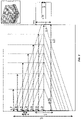
- the spot size converter comprises a shoulder and seven stages. In some embodiments, more or fewer than seven stages are used. Each stage has a beginning width, w-b, which is the most narrow part of the stage. In some embodiments one or more stages have different beginning widths, w-b.
- the shoulder has a thickness t 0 .
- Each stage has a thickness, e.g., measured in a direction normal to a surface of a substrate that the spot size converter is on.
- the first stage has a first thickness, t 1 ; the second stage has a second thickness, t 2 , and so on to the n-th stage.
- Each stage has a length.
- the length of the first stage is L 1
- a 1-stage SSC can include the shoulder and the first stage of SSC 130 . As described below, the same etching process is used to form the waveguide and the 1-stage SSC that includes the first stage and the shoulder of the SSC 130 .
- the shoulder of the SSC has a length L 0 .
- the shoulder of the SSC and the shoulder of the waveguide have substantially the same thickness, and the first stage of the SSC and the ridge of the waveguide have substantially the same thickness.
- Stage 1 thickness, t 1 is equal to a thickness of the ridge of the waveguide. From stage 2, thicknesses of subsequent stages (higher-numbered stages) can be thicker than preceding stages (lower-numbered stages). In some embodiments, the lengths of stages are 50%-90% of the stage below (e.g., directly below).
- a number of stages other than seven for the mode converter are used. Though performance is increased with a higher number of stages, complexity and difficulty in fabricating also increase.
- one or more stages of the ridge include tapers.
- the first stage of the ridge portion of the SSC is configured to taper from a tip at an input end, which is coupled to the ridge of the waveguide, to an expanded width at an output end for coupling to an optical fiber.
- the beginning width of tapers (w-b) (“tips”) may be narrower than 300 nm.
- 300 nm is a dimension of a photolithography lens used to fabricate the device, but tips can be much narrower (e.g., 10 nm).
- edges of tapers may not be as sharp as shown, but instead are somewhat rounded, resulting in a design closer to a vertical taper than what is depicted in the figures.
- FIG. 3 is a longitudinal cross-sectional view diagram illustrating the waveguide and the spot size converter in FIGS. 1 and 2 according to some embodiments of the present invention.
- the left side of the diagram indicates that certain stages can be formed in a front end of the line (FEOL) process or a back end of the line (BEOL) process.
- the FEOL process can include the fabrication of waveguides and other passive optical elements.
- a middle of the line (MOL) process can include the integration of III-V optical chips such as lasers, etc.
- the BEOL process can include the formation of metal wirings, etc.
- the waveguide, the shoulder of the SSC, and stages 1-3 of the SSC are formed during a front end of the line (FEOL) process.
- these elements can be formed using existing processing steps in the FEOL process.
- the stages 4-7 are formed during a back end of the line (FEOL) process, and the device parameters are selected to be compatible with the existing BEOL process.
- the shoulder and ridge of the waveguide and the shoulder can be formed simultaneously using the same etch process.
- the ridge of the waveguide and the ridge of the first stage of the SSC can be formed simultaneously using the same etch process. This process allows portions of the SSC to be formed early in the process flow, and enables the shoulder and stages 1-3 to be formed in the FEOL process.
- Embodiments of the method described here can offer many advantages over conventional processes. In a conventional fabrication process, the waveguide is usually formed in the front end of the process, and the SSC is formed in a back end of the process. In this case, alignment errors between the SSC and waveguide are often unavoidable, causing loss of efficiency.
- the shoulder of the waveguide and the shoulder of the SSC can be simultaneous formed in one simultaneous etching step, and the ridge of the waveguide and the first stage of the SSC can be formed simultaneously in another step.
- the alignment errors between the SSC and the waveguide can be reduced or eliminated.
- testing and detection of defects can be carried out early in the manufacturing process.
- the testing can include testing the waveguide and the SSC by shining light into the waveguide and measuring an output optical signal at an output end of the SSC.
- a first passive test, Passive Test 1 can be carried out after the waveguide and the shoulder and ridge of the first stage of the SSC are formed.
- a light beam can be applied to the input end of the waveguide, and the output light can be detected at the output end of the SSC, for example, by an external waveguide, WG.
- a second passive test, Passive Test 2 can be carried out after stages 2 and 3 of the SSC are formed, for example, by using a first lensed fiber, Lensed Fiber 1, at the output end of the SSC to detect light applied to the waveguide.
- the first lensed fiber can have a diameter of, e.g., 1.5-5.0 ⁇ m, or a diameter that matches the thickness of the SSC including the shoulder and stages 1-4.
- a third passive test, Passive Test 3 can be carried out after stage 4 of the ridge is formed, for example, by using a second lensed fiber, Lensed Fiber 2, at the output end of the SSC to detect light applied to the waveguide.
- the second lensed fiber can have a diameter of, e.g., 2.0-6.0 ⁇ m, or a diameter that matches the thickness of the SSC including the shoulder and stages 1-4, t(s0-s4).
- the early testing can lead to early detection of defects and allow early corrective actions. Subsequently, stages 5-7 can be formed, as described below in connection with FIGS. 6-14 .
- FIG. 4 is a longitudinal cross-sectional view diagram illustrating the optical device of FIG. 1 coupled to an optical fiber according to some embodiments of the present invention.
- FIG. 4 shows a side view of a waveguide and a spot size converter (SSC) optically coupled (e.g., butt coupled) to an optical fiber.
- the waveguide and the SSC are integrated on an SiO 2 layer, BOX, on a handle substrate, Handle Si, in a silicon-on-insulator (SOI) wafer.
- the optical fiber in this case a single mode fiber, SMF, includes cladding regions surrounding a core region 204 .
- the SSC and optical fiber are well matched so that a lens is not used to couple light from the SSC to the optical fiber.
- FIG. 5 is a diagram illustrating simulated optical signal strength along the longitudinal cross section of SSC in the optical device of FIG. 1 according to some embodiments of the present invention.
- a simulated profile of a beam signal strength is shown, with a colored bar on the right indicating optical signal strength represented by each color. It can be seen that the small spot size of the beam with high intensity, at the input end on the left hand side, is expanded as it is transmitted along the longitudinal direction through the spot size converter. As the spot size of the beam is expanded, the signal strength density is reduced.
- FIGS. 6-15 are cross-sectional and perspective view diagrams illustrating a method for making spot size converter and a waveguide according to some embodiments of the present invention.
- a crystalline device layer for example, a crystalline silicon layer (cSi) 110 , is disposed on a substrate including a buried oxide layer (BOX) 150 on a handler substrate 160 .
- this device structure may be provided by a silicon-on-insulator (SOI) wafer.
- SOI silicon-on-insulator
- an oxide layer 102 is formed on a crystalline silicon layer (cSi) 110 .
- the oxide layer can have a thickness in the range of 100-350 nm.
- the oxide layer 102 is removed in preparation for the formation of an amorphous silicon region.
- the oxide layer 102 is used as mask layer, which can be patterned using a photoresist in a lithography process.
- the portion of the crystalline silicon layer (cSi) 110 not protected by the oxide layer 102 is removed by an etching process to form a recess.
- the recess is filled with a non-crystalline layer of material and then planarized.
- the non-crystalline layer is an amorphous silicon layer (a-Si).
- the non-crystalline layer can be made of polysilicon.
- the remaining portion of oxide layer 102 is removed, and a hard mask layer 104 is deposited.
- the hard mask can be made of a material suitable for an etch mask, for example, silicon oxide, silicon nitride, etc.
- the hard mask can be patterned and used to carry out an etching process to simultaneously etch the non-crystalline silicon layer and the crystalline silicon layer.
- FIG. 10 shows examples of structures that can be formed using a simultaneous etching process.
- the lower diagram in FIG. 10 shows a cross sectional view along the length of the device structure of FIG. 9 .
- the upper diagram in FIG. 10 shows cross sectional views of several possible device structures across the device structure of FIG. 9 in a perpendicular direction.
- structure B in the amorphous region and structure D in the crystalline silicon region can be made simultaneously using a single etching step.
- Structure A in the amorphous region and structure C in the crystalline silicon region can be made simultaneously in a two-step etching process.
- structure A in the amorphous region and structure C in the crystalline silicon region can be made simultaneously in a single etching process, if the lower half of the structures have already been formed separately.
- FIGS. 11-13 illustrate a method for forming a waveguide and an SSC using a simultaneous etching process described above.
- FIG. 11 is a perspective view diagram illustrating a structure, in which an amorphous silicon region and a crystalline silicon region have been formed on a substrate, corresponding to the structure in FIG. 8 with the oxide layer removed. As shown below, a shoulder of thickness t 0 and a ridge of thickness t 1 will be formed in the amorphous silicon region and the crystalline silicon region, which has a total thickness of t 0 +t 1 .
- FIG. 12 is a perspective view diagram illustrating a structure, in which a hard mask layer 104 is deposited and patterned on the amorphous silicon region and the crystalline silicon region, corresponding to the structure in FIG. 9 with the hard mask having been patterned.
- FIG. 13 is a perspective view diagram illustrating a structure, in which an amorphous silicon region and a crystalline silicon region have been etched using the hard mask 104 and a simultaneous etching process corresponding to an etched structure in FIG. 10 .
- the etch process removed top portions of the amorphous silicon region and crystalline silicon region to form a shoulder of thickness t 0 and a ridge of thickness t 1 .
- FIG. 14 is a perspective view diagram illustrating a structure, in which the hard mask has been removed from the structure in FIG. 13 , corresponding to the structures A and C in FIG. 10 without the etch mask. It can be seen that ridges and shoulders are formed in both the amorphous silicon region and the crystalline silicon region. In this etching process, the top portions of both the amorphous silicon region and the crystalline silicon region not protected by the patterned hard mask are removed to form a ridge. The depth of the etch can be controlled by end-point detection or by a timed etching process. The shoulders of the crystalline Si waveguide and the SSC can be formed simultaneously in a similar manner by a single etch process.
- the self-aligned method of forming the first stage of the SSC and the waveguide simultaneously using the same etching processes can avoid alignment errors. Further, by forming the SSC along with the waveguide in an early part of the process flow, testing and detection of defects can be carried out early in the process to avoid costly mistakes further into the manufacturing process.
- a dielectric layer 106 is deposited on the device structures in FIGS. 10 and 14 .
- the dielectric layer is then planarized, e.g., using a CMP process.
- additional stages of the SSC can be formed, as described in the examples below.
- FIG. 16 is a perspective view diagram illustrating a spot size converter according to some embodiments of the present invention.
- optical device 1600 includes a waveguide and spot size converter (SSC) integrated on a substrate.
- the shoulder in the waveguide has thickness of t 0
- the ridge of the waveguide has a thickness of t 1 .
- the shoulder in the SSC has a thickness t 0
- the first stage of the SSC has a thickness t 1 .
- the ridge of the waveguide and the first stage of the SSC in FIG. 16 can be formed using a self-aligned process described above as can be the shoulder of the waveguide and the shoulder of the SSC. Unlike the device in FIG.
- the shoulder of the SSC has an initial width at the input end that matches the width of the shoulder of the waveguide, and the shoulder of the SSC tapers and expands to a wider dimension at the output end.
- Two more stages are formed over the first stage of the SSC.
- a second stage has a length of L 2 and a thickness of t 2
- a third stage has a length of L 3 and a thickness t 3 .
- the two additional stages both taper to greater widths at the output end.
- These two additional stages can be formed by forming a patterned recess in the dielectric layer covering the first stage of the SSC and the waveguide.
- Optical device 1600 shown in FIG. 16 can be tested by coupling to a lensed fiber in passive test 2 as described above in connection to FIG. 3 .
- FIG. 17 is a diagram illustrating light transmission through the taper as a function of the taper length of the longest stage of the 3-stage spot size converter of FIG. 16 .
- the vertical axis shows the light transmission through the taper
- the horizontal axis shows the length of the taper. It can be seen that, after the taper length reaches about 100 ⁇ m, the light transmission does not appear to be sensitive to the change in taper length.
- FIG. 18 is a diagram of light coupling between the spot size converter facet and a lensed fiber with a spot size of 2.5 ⁇ m as a function of the SSC waist width shown in FIG. 16 .
- the vertical axis shows the light coupling through the facet
- the horizontal axis shows the width of the waist of the facet.
- the waist refers to the region of the first stage at the output end of the SSC. It can be seen that light coupling appears to reach a peak at a waist width of about 4.2 ⁇ m, and only exhibits small variations in the plotted width range.
- FIGS. 19 and 20 are a graph illustrating simulated optical signal strength along the longitudinal cross section of the spot size converter of FIG. 16 for three different taper lengths, 200 ⁇ m, 300 ⁇ m, and 1000 ⁇ m.
- simulated profiles of a beam signal strength are shown, with a colored bar on the right indicating optical signal strength represented by each color. It can be seen that the small spot size of the beam with high intensity, at the input end on the left-hand side, is expanded as it is transmitted along the longitudinal direction through the spot size converter.
- These plots demonstrate that the fundamental mode evolves adiabatically without cross coupling out of the fundamental mode to higher order modes.
- the actual device can be considerably shorter than 1 mm;
- FIG. 17 suggests that a length of 150 ⁇ m or 200 ⁇ m would be sufficient;
- FIG. 20 demonstrates that the structure of Fi 16 will not couple power into higher order modes.
- FIG. 21 is a perspective view diagram illustrating a 4-stage spot size converter (SSC) according to some embodiments of the present invention.
- optical device 2100 includes a waveguide and spot size converter (SSC) integrated on a substrate.
- SSC waveguide and spot size converter
- Optical device 2100 is similar to optical device 1600 in FIG. 16 , with one additional stage formed over the structure of optical device 1600 .
- the fourth stage has a length of L 4 and a thickness t 4 , and tapers to greater widths at the output end.
- the ridge of the waveguide and the first stage of the ridge portion of the SSC in FIG. 21 can be formed using a self-aligned process described above as can be the shoulder of the waveguide and the shoulder of the SSC.
- optical device 2100 shown in FIG. 21 can be tested by coupling to a lensed fiber in passive test 3 as described above in connection to FIG. 3 .
- FIG. 22 is a diagram of light transmission through the taper as a function of the taper length of the spot size converter of FIG. 21 .
- the vertical axis shows the light transmission through the taper
- the horizontal axis shows the length of the taper of the longest stage. It can be seen that, after the taper length reaches about 250 ⁇ m, the light transmission does not vary much with the change in taper length.
- FIG. 23 is a diagram of light coupling between the spot size converter facet and a lensed fiber with a 3.5 ⁇ m spot size as a function of the SSC waist width shown in FIG. 21 .
- the vertical axis shows the light coupling through the facet
- the horizontal axis shows width of the waist of the facet. It can be seen that light transmission appears to reach a peak at a waist width of about 5.8 ⁇ m, and only exhibits small variations in the plotted width range.
- FIG. 24 is another perspective view diagram illustrating the spot size converter of FIG. 21 according to some embodiments of the present invention.
- FIG. 24 shows a perspective view of the 4-stage spot size converter of FIG. 21 from the output end.
- FIG. 25 is a perspective view diagram illustrating a 7-stage spot size converter according to some embodiments of the present invention.
- optical device 2500 includes a waveguide and a seven-stage spot size converter (SSC) integrated on a substrate.
- SSC spot size converter
- Optical device 2500 is similar to optical device 2100 in FIG. 21 , with three additional stages formed over the structure of optical device 2100 .
- the ridge of the waveguide and the first stage of the SSC in FIG. 25 can be formed using a self-aligned process described above.
- the additional seven stages can be formed using the method described in U.S. application Ser. No. 14/615,942, filed on Feb. 6, 2015, incorporated by reference in its entirety for all purposes.
- FIG. 26 is a diagram of light transmission through the taper as a function of the taper length of the spot size converter of FIG. 25 .
- the vertical axis shows the light transmission through the taper
- the horizontal axis shows plots of light transmission through the taper versus the length of the taper of the longest stage.
- Two plots are shown for two devices having different tip widths, w-b. It can be seen that, after the taper length reaches 1000 ⁇ m, the light transmission varies less with the change in taper length. Further, the light transmission appears to be insensitive to variations in the tip width.
- FIG. 27 is a diagram of light coupling between the SSC facet and a cleaved facet of a single mode fiber as a function of the SSC waist width shown in FIG. 25 .
- the vertical axis shows the light coupling through the facet
- the horizontal axis shows width of the waist of the facet.
- the waist refers to the region of the first stage of the SSC at the output end. It can be seen that light transmission appears to reach a peak at a waist width of about 14.1 ⁇ m, and only exhibits small variations in the plotted width range.
Landscapes
- Physics & Mathematics (AREA)
- Engineering & Computer Science (AREA)
- Microelectronics & Electronic Packaging (AREA)
- General Physics & Mathematics (AREA)
- Optics & Photonics (AREA)
- Power Engineering (AREA)
- Optical Integrated Circuits (AREA)
- Optical Couplings Of Light Guides (AREA)
Abstract
Description
| Dimension | Example Ranges (μm) | Example Values (μm) | ||
| L1 | 200-1200 | 930, 1000, 1100, 1200 | ||
| L2 | 200-1400 | 930, 1000, 1100, 1200 | ||
| L3 | 200-1080 | 917, 925, 933 | ||
| L4 | 100-975 | 782, 800, 833 | ||
| L5 | 100-880 | 708, 725, 728 | ||
| L6 | 100-790 | 484, 500, 521 | ||
| L7 | 50-710 | 300, 333, 350 | ||
| t1 | 0.75-2.25 | 1.0, 1.5, 1.75 | ||
| t2 | 0.3-1.5 | 0.6, 0.7, 0.8 | ||
| t3 | 0.5-2.2 | 1.0, 1.1, 1.2 | ||
| t4 | 0.9-3.6 | 1.5, 1.6, 1.8 | ||
| t5 | 1.1-3.8 | 2.0, 2.1, 2.2 | ||
| t6 | 1.3-4.3 | 2.3, 2.5, 2.6 | ||
| t7 | 1.5-4.6 | 2.8, 2.9, 3.0 | ||
| t(s0-s4) | 2.0-6.5 | 3.0, 3.9, 4.4, 4.9, 5.8, 6 | ||
| t(s5-s7) | 3.0-9.5 | 5.0, 6.0, 6.5, 7.6, 8.9 | ||
| t(total) | 8-17 | 12, 12.5, 12.9 | ||
| w-r | 0.75-3.5, 1.2-2.0 | 1.3, 1.5, 1.75, 2.0 | ||
| w-s | 0.75-4.5 | 2.5, 3, 3.5 | ||
| w1 | 8-15 | 11.5, 11.7, 12, 12.7 | ||
| w7 | 9-20 | 12, 14.1, 14.3, 15 | ||
| w-delta | 0.1-0.5 | 0.2, 0.3, 0.4 | ||
| w-b | 0.0-1.0 | 0.3, 0.4, 0.5, 0.9 | ||
Claims (12)
Priority Applications (1)
| Application Number | Priority Date | Filing Date | Title |
|---|---|---|---|
| US16/777,727 US11360263B2 (en) | 2019-01-31 | 2020-01-30 | Self-aligned spot size converter |
Applications Claiming Priority (2)
| Application Number | Priority Date | Filing Date | Title |
|---|---|---|---|
| US201962799581P | 2019-01-31 | 2019-01-31 | |
| US16/777,727 US11360263B2 (en) | 2019-01-31 | 2020-01-30 | Self-aligned spot size converter |
Publications (2)
| Publication Number | Publication Date |
|---|---|
| US20200301072A1 US20200301072A1 (en) | 2020-09-24 |
| US11360263B2 true US11360263B2 (en) | 2022-06-14 |
Family
ID=72514074
Family Applications (1)
| Application Number | Title | Priority Date | Filing Date |
|---|---|---|---|
| US16/777,727 Active US11360263B2 (en) | 2019-01-31 | 2020-01-30 | Self-aligned spot size converter |
Country Status (1)
| Country | Link |
|---|---|
| US (1) | US11360263B2 (en) |
Families Citing this family (3)
| Publication number | Priority date | Publication date | Assignee | Title |
|---|---|---|---|---|
| US10649148B2 (en) * | 2017-10-25 | 2020-05-12 | Skorpios Technologies, Inc. | Multistage spot size converter in silicon photonics |
| US11360263B2 (en) | 2019-01-31 | 2022-06-14 | Skorpios Technologies. Inc. | Self-aligned spot size converter |
| CN112859239B (en) * | 2021-02-03 | 2022-05-17 | 中国科学技术大学 | InP-based spot size converter, spot size conversion structure and preparation method |
Citations (238)
| Publication number | Priority date | Publication date | Assignee | Title |
|---|---|---|---|---|
| US4182545A (en) | 1977-05-27 | 1980-01-08 | Harris Corporation | Optical coupler system |
| US4293826A (en) | 1979-04-30 | 1981-10-06 | Xerox Corporation | Hybrid semiconductor laser/detectors |
| US4389567A (en) | 1979-06-07 | 1983-06-21 | U.S. Philips Corporation | Semiconductor switching device for guiding and amplifying radiation |
| US4773720A (en) | 1986-06-03 | 1988-09-27 | General Electric Company | Optical waveguide |
| US4799749A (en) | 1985-02-25 | 1989-01-24 | Siemens Aktiengesellschaft | Integrated resonator matrix for wavelength-selective separation or joining of channels in the frequency domain of optical communications technology |
| US4886538A (en) | 1987-07-28 | 1989-12-12 | Polaroid Corporation | Process for tapering waveguides |
| US4932032A (en) | 1989-08-03 | 1990-06-05 | At&T Bell Laboratories | Tapered semiconductor waveguides |
| US5078516A (en) | 1990-11-06 | 1992-01-07 | Bell Communications Research, Inc. | Tapered rib waveguides |
| US5190883A (en) | 1990-05-21 | 1993-03-02 | France Telecom-Establissement autonome de droit Public (Centre National d'Et | Method for making an integrated light guide detector structure made of a semiconductive material |
| US5319667A (en) | 1992-04-10 | 1994-06-07 | Alcatel N.V. | Tunable semiconductor laser |
| US5333219A (en) | 1992-12-17 | 1994-07-26 | At&T Bell Laboratories | Asymmetric Y-branch optical device |
| US5454058A (en) | 1990-03-30 | 1995-09-26 | Bt&D Technologies, Ltd. | Selective optical signal switch and/or combiner |
| EP0696747A2 (en) | 1994-08-12 | 1996-02-14 | Mitsubishi Denki Kabushiki Kaisha | Integrated semiconductor optical waveguide device and fabrication methode |
| US5574742A (en) | 1994-05-31 | 1996-11-12 | Lucent Technologies Inc. | Tapered beam expander waveguide integrated with a diode laser |
| US5579424A (en) | 1993-06-18 | 1996-11-26 | Siemens Aktiengesellschaft | Arrangement for an optical coupling of a fiber to a planar optical waveguide and a method of forming the arrangement |
| US5586209A (en) | 1993-11-01 | 1996-12-17 | Sumitomo Electric Industries, Ltd. | Optical branching device |
| US5633512A (en) | 1990-05-23 | 1997-05-27 | Canon Kabushiki Kaisha | Semiconductor device for varying the mobility of electrons by light irradiation |
| JPH09197179A (en) | 1996-01-19 | 1997-07-31 | Nec Corp | Optical circuit and its production |
| US5745614A (en) | 1995-09-26 | 1998-04-28 | Alcatel N.V. | Optical mode filter |
| US5818989A (en) | 1996-03-27 | 1998-10-06 | Nec Corporation | Branching/crossed optical waveguide circuit |
| US5838070A (en) | 1995-12-28 | 1998-11-17 | Sanyo Electric Co., Ltd. | Apparatus having a substrate and electronic circuit solder-connected with the substrate |
| US5858814A (en) | 1996-07-17 | 1999-01-12 | Lucent Technologies Inc. | Hybrid chip and method therefor |
| US5981400A (en) | 1997-09-18 | 1999-11-09 | Cornell Research Foundation, Inc. | Compliant universal substrate for epitaxial growth |
| US5987050A (en) | 1998-11-16 | 1999-11-16 | Lucent Technologies, Inc. | Laser transmitter based on a coupler and having a controlled output port |
| US5987046A (en) | 1993-08-31 | 1999-11-16 | Fujitsu Limited | Optical semiconductor device and a method of manufacturing the same |
| JP2000089054A (en) | 1998-09-12 | 2000-03-31 | Korea Electronics Telecommun | Method for manufacturing substrate for hybrid optical integrated circuit using SOI optical waveguide |
| US6101210A (en) | 1998-07-10 | 2000-08-08 | Bookham Technology Plc | External cavity laser |
| US6108478A (en) | 1997-02-07 | 2000-08-22 | Bookham Technology Limited | Tapered rib waveguide |
| US6118978A (en) | 1998-04-28 | 2000-09-12 | Hughes Electronics Corporation | Transverse-electric mode filters and methods |
| US6192058B1 (en) | 1998-09-18 | 2001-02-20 | Sarnoff Corporation | Multiwavelength actively mode-locked external cavity semiconductor laser |
| US6229792B1 (en) | 1993-11-01 | 2001-05-08 | Xircom, Inc. | Spread spectrum communication system |
| US6229947B1 (en) | 1997-10-06 | 2001-05-08 | Sandia Corporation | Tapered rib fiber coupler for semiconductor optical devices |
| US20010010743A1 (en) | 2000-02-02 | 2001-08-02 | Ian Cayrefourcq | Passive alignment using slanted wall pedestal |
| US20010026670A1 (en) | 2000-03-28 | 2001-10-04 | Matsushita Electric Industrial Co., Ltd. | Optical waveguide and method for making the same |
| US6310995B1 (en) | 1998-11-25 | 2001-10-30 | University Of Maryland | Resonantly coupled waveguides using a taper |
| US20010036681A1 (en) | 1996-10-31 | 2001-11-01 | Norihiro Iwai | Structure and method for manufacturing a semiconductor optical waveguide |
| US6339606B1 (en) | 1998-06-16 | 2002-01-15 | Princeton Lightwave, Inc. | High power semiconductor light source |
| US20020039469A1 (en) | 2000-10-02 | 2002-04-04 | Jong Sool Jeong | Spot size converter and method of manufacturing the same |
| US20020064337A1 (en) | 2000-11-29 | 2002-05-30 | Behrang Behin | MEMS mirrors with precision clamping mechanism |
| US20020097962A1 (en) | 1998-10-09 | 2002-07-25 | Tetsuzo Yoshimura | Single and multilayer waveguides and fabrication process |
| US20020131744A1 (en) | 2001-03-16 | 2002-09-19 | Bookham Technology Plc | Optical waveguide structure |
| US20020197013A1 (en) | 2001-06-13 | 2002-12-26 | Ansheng Liu | Method and apparatus for tuning a laser with a bragg grating in a semiconductor substrate |
| US6509139B1 (en) | 1999-10-13 | 2003-01-21 | Bookham Technology Plc | Method of fabricating an integrated optical component |
| WO2003012512A1 (en) | 2001-07-30 | 2003-02-13 | Nanyang Technological University | High density fibre coupling |
| US20030035446A1 (en) | 2001-07-13 | 2003-02-20 | Giora Griffel | Frequency selective tunable mirror and applications thereof |
| US20030042494A1 (en) | 2001-09-04 | 2003-03-06 | Worley Eugene Robert | Opto-coupler based on integrated forward biased silicon diode LED |
| JP2003078530A (en) | 2001-08-30 | 2003-03-14 | Matsushita Electric Ind Co Ltd | Wireless communication system |
| US20030081877A1 (en) | 2001-10-29 | 2003-05-01 | Fujitsu Limited | Optical circuit and manufacturing method of the same |
| US6571039B1 (en) | 1999-11-23 | 2003-05-27 | Lnl Technologies, Inc. | Optical waveguide having a weakly-confining waveguide section and a strongly-confining waveguide section optically coupled by a tapered neck |
| US20030129660A1 (en) | 2001-12-10 | 2003-07-10 | Alexander Zien | Efficient method for the joint analysis of molecular expression data and biological networks |
| US20030128724A1 (en) | 2001-09-10 | 2003-07-10 | Imec Vzw | Widely tunable twin guide laser structure |
| US20030138216A1 (en) | 2002-01-15 | 2003-07-24 | Nec Corporation | Optical coupling device and process for fabrication thereof |
| US20030210725A1 (en) | 2001-03-14 | 2003-11-13 | Corning Incorporated, A New York Corporation | Planar laser |
| US20040017962A1 (en) | 2002-07-26 | 2004-01-29 | Lee Kevin K. | Integrated mode converter, waveguide, and on-chip function |
| US20040017976A1 (en) | 2000-12-14 | 2004-01-29 | Hui Luo | Optical waveguide termination with vertical and horizontal mode shaping |
| US20040022223A1 (en) | 2002-08-05 | 2004-02-05 | Harris Corporation | Monitoring link quality in a mobile ad hoc network |
| US6690857B2 (en) | 2000-07-12 | 2004-02-10 | Oluma, Inc. | Fiber devices having side evanescent coupling port |
| US20040037342A1 (en) | 2002-08-22 | 2004-02-26 | Blauvelt Henry A. | Grating-stabilized semiconductor laser |
| US6714566B1 (en) | 1999-03-01 | 2004-03-30 | The Regents Of The University Of California | Tunable laser source with an integrated wavelength monitor and method of operating same |
| US20040062485A1 (en) | 2002-06-21 | 2004-04-01 | Kamelian Limited, A Corporation Of The United Kingdom | Reduction of Truncation loss of a tapered active waveguide |
| US20040066999A1 (en) | 2002-10-04 | 2004-04-08 | Sakamoto Steven R. | Optically induced total internal reflection X-junction waveguide optical switch, network and optical switching method |
| US20040077135A1 (en) | 2002-06-17 | 2004-04-22 | Kopin Corporation | Light-emitting diode device geometry |
| US6728279B1 (en) | 1999-05-17 | 2004-04-27 | Interuniversitair Microelektronica Centrum | Widely wavelength tunable integrated semiconductor device and method for widely tuning semiconductor devices |
| US20040111397A1 (en) | 2002-12-06 | 2004-06-10 | International Business Machines Corporation | Method and apparatus for fusing context data |
| US20040114872A1 (en) | 2002-11-25 | 2004-06-17 | Matsushita Electric Industrial Co., Ltd. | Optical functional device and optical module |
| US20040120675A1 (en) | 2002-12-24 | 2004-06-24 | Michael Skinner | Waveguides with optical monitoring |
| US20040120646A1 (en) | 2002-11-05 | 2004-06-24 | Pentax Corporation | Optical fiber and method for producing the same |
| US20040120648A1 (en) | 2002-12-16 | 2004-06-24 | Kwon Yong Hwan | Spot size converter and method for manufacturing the same, and spot size converter integrated photodetector |
| US6768855B1 (en) | 2001-07-05 | 2004-07-27 | Sandia Corporation | Vertically-tapered optical waveguide and optical spot transformer formed therefrom |
| US20040165812A1 (en) | 2003-01-24 | 2004-08-26 | Blauvelt Henry A. | Etched-facet semiconductor optical component with integrated end-coupled waveguide and methods of fabrication and use thereof |
| US20040182914A1 (en) | 2003-03-19 | 2004-09-23 | Emcore Corporation | Flip-chip light emitting diode with a thermally stable multiple layer reflective p-type contact |
| US20040202440A1 (en) | 2003-04-11 | 2004-10-14 | Prakash Gothoskar | Mode transformation and loss reduction in silicon waveguide structures utilizing tapered transition regions |
| US20040228384A1 (en) | 2003-05-15 | 2004-11-18 | Su-Hwan Oh | Widely tunable sampled-grating distributed feedback laser diode |
| US6829561B2 (en) | 2002-03-16 | 2004-12-07 | International Business Machines Corporation | Method for determining a quality for a data clustering and data processing system |
| US20040245425A1 (en) | 2003-05-23 | 2004-12-09 | Franco Delpiano | Hermetic mounting arrangement for optical and optoelectronic sub-assemblies |
| US20040259279A1 (en) | 2003-04-15 | 2004-12-23 | Erchak Alexei A. | Light emitting device methods |
| US20040258360A1 (en) | 2003-03-25 | 2004-12-23 | Lim Desmond R. | External gain element with mode converter and high index contrast waveguide |
| US20040264840A1 (en) | 2001-02-11 | 2004-12-30 | Tony Mule | Guided-wave optical interconnections embedded within a microelectronic wafer-level batch package |
| US6846694B2 (en) | 2002-03-11 | 2005-01-25 | Sharp Kabushiki Kaisha | Semiconductor device with built-in light receiving element, production method thereof, and optical pickup incorporating the same |
| US20050033858A1 (en) | 2000-07-19 | 2005-02-10 | Swildens Eric Sven-Johan | Load balancing service |
| US20050058416A1 (en) | 2001-08-02 | 2005-03-17 | Hoon Lee Howard Wing | Optical devices with engineered nonlinear nanocomposite materials |
| US20050082552A1 (en) | 2003-10-21 | 2005-04-21 | Ming Fang | Large bumps for optical flip chips |
| US6888989B1 (en) | 2001-12-11 | 2005-05-03 | Phosistor Technologies, Inc. | Photonic chip mounting in a recess for waveguide alignment and connection |
| US20050105853A1 (en) | 2003-11-13 | 2005-05-19 | Ansheng Liu | Method and apparatus for dual tapering an optical waveguide |
| US20050123244A1 (en) | 2003-12-03 | 2005-06-09 | Block Bruce A. | Embedded optical waveguide coupler |
| US6931178B2 (en) | 2003-01-10 | 2005-08-16 | Honeywell International Inc. | Coupling a tapered optical element to an optical fiber |
| US20050185893A1 (en) | 2004-02-20 | 2005-08-25 | Ansheng Liu | Method and apparatus for tapering an optical waveguide |
| US20050202554A1 (en) | 2000-12-14 | 2005-09-15 | Hui Luo | Optical waveguide termination with vertical and horizontal mode shaping |
| US20050211465A1 (en) | 2004-03-29 | 2005-09-29 | Shinko Electric Industries Co., Ltd. | Electronic parts packaging structure and method of manufacturing the same |
| US20050213618A1 (en) | 2004-03-29 | 2005-09-29 | Sochava Sergei L | Semi-integrated designs for external cavity tunable lasers |
| US20050211993A1 (en) | 2002-01-28 | 2005-09-29 | Masahiko Sano | Opposed terminal structure having a nitride semiconductor element |
| US20050226284A1 (en) | 2004-04-13 | 2005-10-13 | Fujitsu Limited | Wavelength tunable laser of small size |
| US6956983B2 (en) | 2002-05-31 | 2005-10-18 | Intel Corporation | Epitaxial growth for waveguide tapering |
| US20050286426A1 (en) | 2004-06-23 | 2005-12-29 | Microsoft Corporation | System and method for link quality routing using a weighted cumulative expected transmission time metric |
| US20060002443A1 (en) | 2004-06-30 | 2006-01-05 | Gennady Farber | Multimode external cavity semiconductor lasers |
| US7006746B2 (en) | 2002-08-29 | 2006-02-28 | Micron Technology, Inc. | Waveguide for thermo optic device |
| US20060045157A1 (en) | 2004-08-26 | 2006-03-02 | Finisar Corporation | Semiconductor laser with expanded mode |
| US7016560B2 (en) | 2001-02-28 | 2006-03-21 | Lightwave Microsystems Corporation | Microfluidic control for waveguide optical switches, variable attenuators, and other optical devices |
| US20060093002A1 (en) | 2004-11-03 | 2006-05-04 | Park Mahn Y | Hybrid type integrated optical device |
| US20060104322A1 (en) | 2004-11-18 | 2006-05-18 | Park Mahn Y | Temperature-independent external cavity laser |
| US20060109542A1 (en) | 2003-01-15 | 2006-05-25 | Matsushita Electric Industrial Co., Ltd. | Optical waveguide device, optical waveguide laser using the same and optical apparatus having same |
| US20060115215A1 (en) | 2004-11-30 | 2006-06-01 | Ansheng Liu | Dual "cheese wedge" silicon taper waveguide |
| JP2006186446A (en) | 2004-12-27 | 2006-07-13 | Hiroshima Industrial Promotion Organization | Communication method |
| US7079727B1 (en) * | 2002-10-09 | 2006-07-18 | Little Optics, Inc. | Integrated optical mode shape transformer and method of fabrication |
| US7082235B2 (en) | 2001-09-10 | 2006-07-25 | California Institute Of Technology | Structure and method for coupling light between dissimilar waveguides |
| US7120336B2 (en) | 2002-08-29 | 2006-10-10 | Micron Technology, Inc. | Resonator for thermo optic device |
| US20060285797A1 (en) | 2003-10-09 | 2006-12-21 | Little Brent E | Integrated optical mode shape transformer and method of fabrication |
| US20070002924A1 (en) | 2005-06-30 | 2007-01-04 | Hutchinson John M | Integrated monitoring and feedback designs for external cavity tunable lasers |
| JP2007074202A (en) | 2005-09-06 | 2007-03-22 | Nippon Telegr & Teleph Corp <Ntt> | Quality measuring method and node device |
| US7257283B1 (en) | 2006-06-30 | 2007-08-14 | Intel Corporation | Transmitter-receiver with integrated modulator array and hybrid bonded multi-wavelength laser array |
| US20070223549A1 (en) | 2006-03-23 | 2007-09-27 | Nl Nanosemiconductor Gmbh | High-Power Optoelectronic Device with Improved Beam Quality Incorporating A Lateral Mode Filtering Section |
| US20070280326A1 (en) | 2005-12-16 | 2007-12-06 | Sioptical, Inc. | External cavity laser in thin SOI with monolithic electronics |
| US20080002928A1 (en) | 2006-06-05 | 2008-01-03 | Bing Li | Single mode photonic circuit architecture and a new optical splitter design based on parallel waveguide mode conversion |
| US7317853B2 (en) | 2003-08-19 | 2008-01-08 | Ignis Technologies As | Integrated optics spot size converter and manufacturing method |
| US7326611B2 (en) | 2005-02-03 | 2008-02-05 | Micron Technology, Inc. | DRAM arrays, vertical transistor structures and methods of forming transistor structures and DRAM arrays |
| US7359588B2 (en) | 2004-12-14 | 2008-04-15 | Electronics And Telecommunications Research Institute | Electroabsorption modulator and method of manufacturing the same |
| US20080266639A1 (en) | 2004-04-30 | 2008-10-30 | Andrea Melloni | Optical Device Based on a Three-Arm Mach-Zehnder Interferometer |
| US7464147B1 (en) | 1999-11-10 | 2008-12-09 | International Business Machines Corporation | Managing a cluster of networked resources and resource groups using rule - base constraints in a scalable clustering environment |
| US20090016399A1 (en) | 2006-04-26 | 2009-01-15 | The Regents Of The University Of California | Hybrid silicon evanescent photodetectors |
| US20090020499A1 (en) | 2005-03-31 | 2009-01-22 | Alessandro Nottola | Method to Fabricate a Redirecting Mirror in Optical Waveguide Devices |
| US20090087137A1 (en) | 2007-10-02 | 2009-04-02 | My The Doan | Planar lightwave circuits with air filled trenches |
| US7519257B2 (en) | 2004-11-24 | 2009-04-14 | Cornell Research Foundation, Inc. | Waveguide structure for guiding light in low-index material |
| US7531395B2 (en) | 2004-09-01 | 2009-05-12 | Micron Technology, Inc. | Methods of forming a layer comprising epitaxial silicon, and methods of forming field effect transistors |
| US7539373B1 (en) | 2007-11-26 | 2009-05-26 | Onechip Photonics Inc. | Integrated lateral mode converter |
| US20090135861A1 (en) | 2007-11-09 | 2009-05-28 | Lightwire, Inc. | Soi-based tunable laser |
| US20090225796A1 (en) | 2008-03-10 | 2009-09-10 | Sumitomo Electric Industries, Ltd. | Diffraction grating device, laser diode, and wavelength tunable filter |
| US7598527B2 (en) | 2004-01-20 | 2009-10-06 | Binoptics Corporation | Monitoring photodetector for integrated photonic devices |
| US20090267173A1 (en) | 2008-03-27 | 2009-10-29 | Hidekazu Takahashi | Semiconductor device and method for manufacturing semiconductor device |
| US20090278233A1 (en) | 2007-07-26 | 2009-11-12 | Pinnington Thomas Henry | Bonded intermediate substrate and method of making same |
| US20090294803A1 (en) | 2004-06-04 | 2009-12-03 | The Board Of Trustees Of The University Of Illinois | Methods and devices for fabricating and assembling printable semiconductor elements |
| US7633988B2 (en) | 2003-07-31 | 2009-12-15 | Jds Uniphase Corporation | Tunable laser source with monolithically integrated interferometric optical modulator |
| US20090310140A1 (en) | 2006-12-01 | 2009-12-17 | 3M Innovative Properties Company | Optical Sensing Devices and Methods |
| US7643710B1 (en) | 2008-09-17 | 2010-01-05 | Intel Corporation | Method and apparatus for efficient coupling between silicon photonic chip and optical fiber |
| EP2141525A1 (en) | 2008-06-30 | 2010-01-06 | International Business Machines Corporation | CMOS compatible integrated dielectric optical waveguide coupler and fabrication |
| CN101637007A (en) | 2007-03-20 | 2010-01-27 | 汤姆森特许公司 | Hierarchically clustered P2P streaming system |
| US20100040327A1 (en) | 2007-03-20 | 2010-02-18 | Yukari Deki | Optical waveguide and spot size converter using the same |
| US20100114846A1 (en) | 2002-10-16 | 2010-05-06 | Microsoft Corporation | Optimizing media player memory during rendering |
| US20100111128A1 (en) | 2008-11-04 | 2010-05-06 | Guogang Qin | SELECTIVE AREA METAL BONDING Si-BASED LASER |
| US20100123145A1 (en) | 2008-11-18 | 2010-05-20 | Sang Youl Lee | Light emitting device and light emitting device package having the same |
| JP2010199972A (en) | 2009-02-25 | 2010-09-09 | Nippon Telegr & Teleph Corp <Ntt> | Path control method, and node device |
| US7796656B2 (en) | 2007-11-05 | 2010-09-14 | Onechip Photonics Inc. | Enhanced efficiency laterally-coupled distributed feedback laser |
| US20100238855A1 (en) | 2008-07-24 | 2010-09-23 | Atsushi Yoshida | Relay device and relay method |
| US20100247037A1 (en) | 2009-03-31 | 2010-09-30 | Infinera Corporation | Optical mode coupler |
| US20100266288A1 (en) | 2001-04-03 | 2010-10-21 | Little Optics, Inc | High efficiency optical mode transformer for matching a single mode fiber to a high index contrast planar waveguide |
| US20100272385A1 (en) | 2005-12-28 | 2010-10-28 | Noriyuki Akiyama | Optical waveguide device and method of manufacturing optical waveguide device |
| US7831116B2 (en) | 2008-06-09 | 2010-11-09 | Samsung Electro-Mechanics Co., Ltd. | Optical waveguide and optical printed circuit board having the same |
| US20100302992A1 (en) | 2009-05-19 | 2010-12-02 | Huawei Technologies Co., Ltd. | Method for sending packet data, base station, and mobile station |
| JP2010281899A (en) | 2009-06-02 | 2010-12-16 | Mitsubishi Electric Corp | Optical filter |
| US20110012261A1 (en) | 2008-01-22 | 2011-01-20 | Samsung Electro-Mechanics | Post bump and method of forming the same |
| US20110032964A1 (en) | 2009-03-04 | 2011-02-10 | Alcatel-Lucent Usa, Incorporated | Fabricating electronic-photonic devices having an active layer with spherical quantum dots |
| US20110044193A1 (en) | 2004-04-02 | 2011-02-24 | Antonio Forenza | Systems and methods to coordinate transmissions in distributed wireless systems via user clustering |
| JP2011075917A (en) | 2009-09-30 | 2011-04-14 | Sumitomo Osaka Cement Co Ltd | Optical waveguide element |
| US20110085760A1 (en) | 2009-10-13 | 2011-04-14 | Electronics And Telecommunications Research Institute | Optical devices and methods of fabricating the same |
| US20110085572A1 (en) | 2009-10-13 | 2011-04-14 | Skorpios Technologies, Inc. | Method and system for hybrid integration of a tunable laser |
| US20110085577A1 (en) | 2009-10-13 | 2011-04-14 | Skorpios Technologies, Inc. | Method and system of heterogeneous substrate bonding for photonic integration |
| WO2011046898A1 (en) | 2009-10-13 | 2011-04-21 | Skorpios Technologies, Inc. | Method and system for hybrid integration of a tunable laser |
| US20110089524A1 (en) | 2009-10-16 | 2011-04-21 | Sumco Corporation | Semiconductor device and method of manufacturing the same |
| US7939934B2 (en) | 2005-03-16 | 2011-05-10 | Tessera, Inc. | Microelectronic packages and methods therefor |
| US20110158584A1 (en) | 2007-10-22 | 2011-06-30 | Massachusetts Institute Of Technology | Low-loss bloch wave guiding in open structures and highly compact efficient waveguide-crossing arrays |
| US7972875B2 (en) | 2007-01-17 | 2011-07-05 | The Board Of Trustees Of The University Of Illinois | Optical systems fabricated by printing-based assembly |
| US20110163444A1 (en) | 2004-12-13 | 2011-07-07 | Renesas Electronics Corporation | Semiconductor device having elastic solder bump to prevent disconnection |
| US20110165707A1 (en) | 2008-05-22 | 2011-07-07 | Connector Optics Llc | Method for attaching optical components onto silicon-based integrated circuits |
| US20110205660A1 (en) | 2010-02-25 | 2011-08-25 | Tdk Corporation | Spot size converter and thermal assist magnetic recording head therewith |
| US20110211604A1 (en) | 2008-05-08 | 2011-09-01 | Universität Ulm | Completely Self-Adjusted Surface-Emitting Semiconductor Laser For Surface Mounting Having Optimized Properties |
| US20110216997A1 (en) | 2003-04-23 | 2011-09-08 | Lightwire, Inc. | Sub-Micron Planar Lightwave Devices Formed on an SOI Optical Platform |
| US20110217002A1 (en) | 2010-03-04 | 2011-09-08 | Attila Mekis | Method and System for Waveguide Mode Filters |
| US8025444B2 (en) | 2006-05-25 | 2011-09-27 | Kyoung Hie CHUNG | Optical module and fabrication method of the same |
| US20110267676A1 (en) | 2009-10-13 | 2011-11-03 | Skorpios Technologies, Inc. | Method and system for hybrid integration of an opto-electronic integrated circuit |
| US20120001166A1 (en) | 2010-06-30 | 2012-01-05 | International Business Machines Corporation | Parellel optical transceiver module |
| US20120002694A1 (en) | 2010-06-30 | 2012-01-05 | The Regents Of The University Of California | Loss modulated silicon evanescent lasers |
| US20120002931A1 (en) | 2009-03-17 | 2012-01-05 | Nec Corporation | Optical waveguide device and method of manufacturing thereof |
| US20120057610A1 (en) | 2009-10-13 | 2012-03-08 | Skorpios Technologies, Inc. | Method and system for hybrid integration of a tunable laser and a phase modulator |
| US20120057816A1 (en) | 2009-10-13 | 2012-03-08 | Skorpios Techologies, Inc. | Method and system for heterogeneous substrate bonding of waveguide receivers |
| US20120057079A1 (en) | 2009-10-13 | 2012-03-08 | Skorpios Technolgies, Inc. | Method and system for hybrid integration of a tunable laser for a cable tv transmitter |
| US20120057609A1 (en) | 2009-10-13 | 2012-03-08 | Skorpios Technologies, Inc. | Method and system for hybrid integration of a tunable laser and a mach zehnder modulator |
| US20120091594A1 (en) | 2010-10-18 | 2012-04-19 | Christof Landesberger | Method of Producing a Chip Package, and Chip Package |
| US20120093456A1 (en) | 2010-10-14 | 2012-04-19 | Universiteit Gent | Coupling Methods and Systems Using a Taper |
| US8170383B2 (en) | 2006-12-01 | 2012-05-01 | Nec Corporation | Optical converter |
| US20120120978A1 (en) | 2009-08-20 | 2012-05-17 | International Business Machines Corporation | 3d optoelectronic packaging |
| WO2012078361A1 (en) | 2010-12-08 | 2012-06-14 | Skorpios Technologies, Inc. | Method and system for template assisted wafer bonding |
| US20120170931A1 (en) | 2010-12-30 | 2012-07-05 | Infinera Corporation | Method and apparatus for local optimization of an optical transmitter |
| US20120189317A1 (en) | 2011-01-20 | 2012-07-26 | John Heck | Hybrid iii-v silicon laser formed by direct bonding |
| US8254735B2 (en) | 2009-09-23 | 2012-08-28 | Agilent Technologies, Inc. | Optical fiber coupler |
| US20120224813A1 (en) | 2011-03-04 | 2012-09-06 | Alcatel-Lucent Usa Inc. | Optical coupler between planar multimode waveguides |
| US20120230635A1 (en) | 2009-09-28 | 2012-09-13 | Haruhiko Yoshida | Optical coupling device and optical coupling-branching device |
| US8271205B2 (en) | 2008-09-19 | 2012-09-18 | Corbett Research Pty Ltd | Method and system for analysis of melt curves, particularly dsDNA and protein melt curves |
| US8290014B2 (en) | 2010-03-11 | 2012-10-16 | Junesand Carl | Active photonic device |
| US8320721B2 (en) | 2008-02-29 | 2012-11-27 | Google Inc. | Optical mode transformer, in particular for coupling an optical fiber and a high-index contrast waveguide |
| US20120320939A1 (en) | 2010-02-24 | 2012-12-20 | Roeland Baets | Laser light coupling into soi cmos photonic integrated circuit |
| US20120321244A1 (en) | 2011-06-15 | 2012-12-20 | Opnext Japan, Inc | Optical semiconductor device, and manufacturing method thereof |
| EP2544319A1 (en) | 2011-07-08 | 2013-01-09 | Alcatel Lucent | Laser source for photonic integrated devices |
| US20130022312A1 (en) | 2011-07-19 | 2013-01-24 | Universiteit Gent | Deep-Shallow Optical Radiation Filters |
| US20130037905A1 (en) | 2011-08-09 | 2013-02-14 | Oracle International Corporation | Hybrid substrateless device with enhanced tuning efficiency |
| US20130051727A1 (en) | 2011-08-30 | 2013-02-28 | Skorpios Technologies, Inc. | Integrated waveguide coupler |
| US20130107741A1 (en) | 2010-04-28 | 2013-05-02 | Telefonaktiebolaget Lm Ericsson (Publ) | Monitoring broadcast and multicast streaming service |
| US20130114924A1 (en) | 2010-04-29 | 2013-05-09 | Agency For Science, Technology And Research | Optical Arrangement and a Method of Forming the Same |
| US20130170793A1 (en) * | 2010-09-28 | 2013-07-04 | Nec Corporation | Optical waveguide structure and optical waveguide device |
| US8483528B2 (en) | 2008-02-29 | 2013-07-09 | Google Inc. | Optical mode transformer, in particular for coupling an optical fiber and a high-index contrast waveguide |
| US8488923B2 (en) | 2010-03-29 | 2013-07-16 | Intel Corporation | Multimode optical coupler interfaces |
| WO2013109955A1 (en) | 2012-01-18 | 2013-07-25 | Skorpios Technologies, Inc. | Vertical integration of cmos electronics with photonic devices |
| US20130216177A1 (en) | 2012-02-17 | 2013-08-22 | Taiwan Semiconductor Manufacturing Company, Ltd. | Method of fabrication polymer waveguide |
| US20130251299A1 (en) | 2012-03-20 | 2013-09-26 | Skorpios Technologies, Inc. | Multi-port optical circulator system |
| US20130266263A1 (en) | 2012-04-04 | 2013-10-10 | Electronics And Telecommunications Research Institute | Spot size converters and methods of manufacturing the same |
| US20130301975A1 (en) | 2012-04-13 | 2013-11-14 | Skorpios Technologies, Inc. | Hybrid optical modulator |
| US8620230B2 (en) | 2007-06-18 | 2013-12-31 | Amichay SANDEROVITZ | Wireless network architecture and method for base station utilization |
| WO2014021411A1 (en) | 2012-08-02 | 2014-02-06 | 独立行政法人産業技術総合研究所 | Optical waveguide and optical waveguide mirror |
| WO2014025824A2 (en) | 2012-08-10 | 2014-02-13 | Skorpios Technologies, Inc. | Method and system for performing testing of photonic devices |
| US20140064658A1 (en) | 2012-08-29 | 2014-03-06 | Anand Ramaswamy | Thermal management for photonic integrated circuits |
| US20140133817A1 (en) | 2011-07-19 | 2014-05-15 | The Centre For Integrated Photonics Ltd. | Coupled Waveguide Apparatus and Structures Therefor |
| KR20140060548A (en) | 2011-09-04 | 2014-05-20 | 가부시키가이샤 도우사 고가쿠 겐큐쇼 | Glycosylated polypeptide and drug composition containing said polypeptide |
| US20140252411A1 (en) | 2013-03-11 | 2014-09-11 | Yimin Kang | Low voltage avalanche photodiode with re-entrant mirror for silicon based photonic integrated circuits |
| US20140270620A1 (en) | 2013-03-14 | 2014-09-18 | Cisco Technology, Inc. | Modal rotation in optical waveguides |
| WO2014176561A1 (en) | 2013-04-25 | 2014-10-30 | Skorpios Technologies, Inc. | Method and system for height registration during chip bonding |
| US20150086153A1 (en) | 2013-09-20 | 2015-03-26 | Oki Electric Industry Co., Ltd. | Optical device having a stepwise or tapered light input/output part and manufacturing method therefor |
| US20150097211A1 (en) | 2013-10-09 | 2015-04-09 | Skorpios Technologies, Inc. | Structures for bonding a direct-bandgap chip to a silicon photonic device |
| US9075192B2 (en) | 2012-09-24 | 2015-07-07 | Finisar Sweden Ab | Optical waveguide splitter |
| US20150219853A1 (en) | 2014-02-06 | 2015-08-06 | Skorpios Technologies, Inc. | Integrated multistage taper coupler for waveguide to fiber coupling |
| US20150234124A1 (en) | 2011-12-27 | 2015-08-20 | Neophotonics Corporation | Integrated circuit coupling system with waveguide circuitry and method of manufacture thereof |
| US20150253472A1 (en) | 2014-03-07 | 2015-09-10 | Skorpios Technologies, Inc. | High-order-mode filter for semiconductor waveguides |
| US20150253471A1 (en) | 2012-09-25 | 2015-09-10 | Nec Corporation | High-order mode filter |
| US20150316723A1 (en) | 2012-12-13 | 2015-11-05 | Geoff W. Taylor | Fiber Optic Coupler Array |
| US9195001B2 (en) | 2011-12-28 | 2015-11-24 | Fujitsu Limited | Spot size converter, optical transmitter, optical receiver, optical transceiver, and method of manufacturing spot size converter |
| US20150346429A1 (en) | 2014-05-27 | 2015-12-03 | Skorpios Technologies, Inc. | Waveguide mode expander using amorphous silicon |
| US20150362673A1 (en) | 2013-07-31 | 2015-12-17 | Oracle International Corporation | Surface-normal coupler for silicon-on-insulator platforms |
| US9274282B2 (en) | 2013-08-23 | 2016-03-01 | Cisco Technology, Inc. | Coupling light from an external source to a waveguide using a multi-step converter |
| US9316785B2 (en) | 2013-10-09 | 2016-04-19 | Skorpios Technologies, Inc. | Integration of an unprocessed, direct-bandgap chip into a silicon photonic device |
| US9316792B2 (en) | 2013-03-25 | 2016-04-19 | Electronics And Telecommunications Research Institute | Optical coupler and optical device including the same |
| US20160124148A1 (en) | 2014-10-31 | 2016-05-05 | Fujitsu Limited | Optical waveguide, spot size converter and optical apparatus |
| US9348099B2 (en) | 2014-07-18 | 2016-05-24 | Intel Corporation | Optical coupler |
| US9354396B2 (en) | 2014-03-17 | 2016-05-31 | Stmicroelectronics (Crolles 2) Sas | Large bandwidth multi-mode interference device |
| US20160170142A1 (en) | 2011-08-30 | 2016-06-16 | Skorpios Technologies, Inc. | Integrated photonics mode expander |
| US9460740B1 (en) | 2015-10-12 | 2016-10-04 | Headway Technologies, Inc. | Thermal assisted magnetic recording spot-size converter with finite ridge width |
| US20160306117A1 (en) | 2015-04-17 | 2016-10-20 | Christopher Middlebrook | Tapered polymer waveguide |
| US20160306111A1 (en) | 2015-04-20 | 2016-10-20 | Skorpios Technologies, Inc. | Back side via vertical output couplers |
| US9529151B2 (en) | 2013-06-27 | 2016-12-27 | Fujikura Ltd. | Polarization conversion element |
| US20170090118A1 (en) | 2014-03-07 | 2017-03-30 | Skorpios Technologies, Inc. | Wide shoulder, high order mode filter for thick-silicon waveguides |
| US10649148B2 (en) | 2017-10-25 | 2020-05-12 | Skorpios Technologies, Inc. | Multistage spot size converter in silicon photonics |
| US20200301072A1 (en) | 2019-01-31 | 2020-09-24 | Skorpios Technologies, Inc. | Self-aligned spot size converter |
-
2020
- 2020-01-30 US US16/777,727 patent/US11360263B2/en active Active
Patent Citations (293)
| Publication number | Priority date | Publication date | Assignee | Title |
|---|---|---|---|---|
| US4182545A (en) | 1977-05-27 | 1980-01-08 | Harris Corporation | Optical coupler system |
| US4293826A (en) | 1979-04-30 | 1981-10-06 | Xerox Corporation | Hybrid semiconductor laser/detectors |
| US4389567A (en) | 1979-06-07 | 1983-06-21 | U.S. Philips Corporation | Semiconductor switching device for guiding and amplifying radiation |
| US4799749A (en) | 1985-02-25 | 1989-01-24 | Siemens Aktiengesellschaft | Integrated resonator matrix for wavelength-selective separation or joining of channels in the frequency domain of optical communications technology |
| US4773720A (en) | 1986-06-03 | 1988-09-27 | General Electric Company | Optical waveguide |
| US4886538A (en) | 1987-07-28 | 1989-12-12 | Polaroid Corporation | Process for tapering waveguides |
| US4932032A (en) | 1989-08-03 | 1990-06-05 | At&T Bell Laboratories | Tapered semiconductor waveguides |
| US5454058A (en) | 1990-03-30 | 1995-09-26 | Bt&D Technologies, Ltd. | Selective optical signal switch and/or combiner |
| US5190883A (en) | 1990-05-21 | 1993-03-02 | France Telecom-Establissement autonome de droit Public (Centre National d'Et | Method for making an integrated light guide detector structure made of a semiconductive material |
| US5633512A (en) | 1990-05-23 | 1997-05-27 | Canon Kabushiki Kaisha | Semiconductor device for varying the mobility of electrons by light irradiation |
| US5078516A (en) | 1990-11-06 | 1992-01-07 | Bell Communications Research, Inc. | Tapered rib waveguides |
| US5319667A (en) | 1992-04-10 | 1994-06-07 | Alcatel N.V. | Tunable semiconductor laser |
| US5333219A (en) | 1992-12-17 | 1994-07-26 | At&T Bell Laboratories | Asymmetric Y-branch optical device |
| US5579424A (en) | 1993-06-18 | 1996-11-26 | Siemens Aktiengesellschaft | Arrangement for an optical coupling of a fiber to a planar optical waveguide and a method of forming the arrangement |
| US5987046A (en) | 1993-08-31 | 1999-11-16 | Fujitsu Limited | Optical semiconductor device and a method of manufacturing the same |
| US6229792B1 (en) | 1993-11-01 | 2001-05-08 | Xircom, Inc. | Spread spectrum communication system |
| US5586209A (en) | 1993-11-01 | 1996-12-17 | Sumitomo Electric Industries, Ltd. | Optical branching device |
| US5574742A (en) | 1994-05-31 | 1996-11-12 | Lucent Technologies Inc. | Tapered beam expander waveguide integrated with a diode laser |
| EP0696747A2 (en) | 1994-08-12 | 1996-02-14 | Mitsubishi Denki Kabushiki Kaisha | Integrated semiconductor optical waveguide device and fabrication methode |
| US5745614A (en) | 1995-09-26 | 1998-04-28 | Alcatel N.V. | Optical mode filter |
| US5838070A (en) | 1995-12-28 | 1998-11-17 | Sanyo Electric Co., Ltd. | Apparatus having a substrate and electronic circuit solder-connected with the substrate |
| JPH09197179A (en) | 1996-01-19 | 1997-07-31 | Nec Corp | Optical circuit and its production |
| US5818989A (en) | 1996-03-27 | 1998-10-06 | Nec Corporation | Branching/crossed optical waveguide circuit |
| US5858814A (en) | 1996-07-17 | 1999-01-12 | Lucent Technologies Inc. | Hybrid chip and method therefor |
| US20010036681A1 (en) | 1996-10-31 | 2001-11-01 | Norihiro Iwai | Structure and method for manufacturing a semiconductor optical waveguide |
| US6108478A (en) | 1997-02-07 | 2000-08-22 | Bookham Technology Limited | Tapered rib waveguide |
| US5981400A (en) | 1997-09-18 | 1999-11-09 | Cornell Research Foundation, Inc. | Compliant universal substrate for epitaxial growth |
| US6229947B1 (en) | 1997-10-06 | 2001-05-08 | Sandia Corporation | Tapered rib fiber coupler for semiconductor optical devices |
| US6118978A (en) | 1998-04-28 | 2000-09-12 | Hughes Electronics Corporation | Transverse-electric mode filters and methods |
| US6339606B1 (en) | 1998-06-16 | 2002-01-15 | Princeton Lightwave, Inc. | High power semiconductor light source |
| US6101210A (en) | 1998-07-10 | 2000-08-08 | Bookham Technology Plc | External cavity laser |
| JP2000089054A (en) | 1998-09-12 | 2000-03-31 | Korea Electronics Telecommun | Method for manufacturing substrate for hybrid optical integrated circuit using SOI optical waveguide |
| US6316281B1 (en) | 1998-09-12 | 2001-11-13 | Electronics And Telecommunications Research Institute | Method for fabricating a hybrid optical integrated circuit employing SOI optical waveguide |
| US6192058B1 (en) | 1998-09-18 | 2001-02-20 | Sarnoff Corporation | Multiwavelength actively mode-locked external cavity semiconductor laser |
| US20020097962A1 (en) | 1998-10-09 | 2002-07-25 | Tetsuzo Yoshimura | Single and multilayer waveguides and fabrication process |
| US5987050A (en) | 1998-11-16 | 1999-11-16 | Lucent Technologies, Inc. | Laser transmitter based on a coupler and having a controlled output port |
| US6310995B1 (en) | 1998-11-25 | 2001-10-30 | University Of Maryland | Resonantly coupled waveguides using a taper |
| US6714566B1 (en) | 1999-03-01 | 2004-03-30 | The Regents Of The University Of California | Tunable laser source with an integrated wavelength monitor and method of operating same |
| US7058096B2 (en) | 1999-05-17 | 2006-06-06 | Interuniversitair Microelektronica Centrum (Imec Vzw) | Widely wavelength tunable integrated semiconductor device and method for widely wavelength tuning semiconductor devices |
| US6728279B1 (en) | 1999-05-17 | 2004-04-27 | Interuniversitair Microelektronica Centrum | Widely wavelength tunable integrated semiconductor device and method for widely tuning semiconductor devices |
| US6509139B1 (en) | 1999-10-13 | 2003-01-21 | Bookham Technology Plc | Method of fabricating an integrated optical component |
| US7464147B1 (en) | 1999-11-10 | 2008-12-09 | International Business Machines Corporation | Managing a cluster of networked resources and resource groups using rule - base constraints in a scalable clustering environment |
| US6571039B1 (en) | 1999-11-23 | 2003-05-27 | Lnl Technologies, Inc. | Optical waveguide having a weakly-confining waveguide section and a strongly-confining waveguide section optically coupled by a tapered neck |
| US20010010743A1 (en) | 2000-02-02 | 2001-08-02 | Ian Cayrefourcq | Passive alignment using slanted wall pedestal |
| US20010026670A1 (en) | 2000-03-28 | 2001-10-04 | Matsushita Electric Industrial Co., Ltd. | Optical waveguide and method for making the same |
| US6690857B2 (en) | 2000-07-12 | 2004-02-10 | Oluma, Inc. | Fiber devices having side evanescent coupling port |
| US20050033858A1 (en) | 2000-07-19 | 2005-02-10 | Swildens Eric Sven-Johan | Load balancing service |
| US20020039469A1 (en) | 2000-10-02 | 2002-04-04 | Jong Sool Jeong | Spot size converter and method of manufacturing the same |
| US20020064337A1 (en) | 2000-11-29 | 2002-05-30 | Behrang Behin | MEMS mirrors with precision clamping mechanism |
| US7251406B2 (en) | 2000-12-14 | 2007-07-31 | Shipley Company, L.L.C. | Optical waveguide termination with vertical and horizontal mode shaping |
| US6987919B2 (en) | 2000-12-14 | 2006-01-17 | Shipley Company, L.L.C. | Optical waveguide termination with vertical and horizontal mode shaping |
| US20050202554A1 (en) | 2000-12-14 | 2005-09-15 | Hui Luo | Optical waveguide termination with vertical and horizontal mode shaping |
| US20040017976A1 (en) | 2000-12-14 | 2004-01-29 | Hui Luo | Optical waveguide termination with vertical and horizontal mode shaping |
| US20040264840A1 (en) | 2001-02-11 | 2004-12-30 | Tony Mule | Guided-wave optical interconnections embedded within a microelectronic wafer-level batch package |
| US7016560B2 (en) | 2001-02-28 | 2006-03-21 | Lightwave Microsystems Corporation | Microfluidic control for waveguide optical switches, variable attenuators, and other optical devices |
| US20030210725A1 (en) | 2001-03-14 | 2003-11-13 | Corning Incorporated, A New York Corporation | Planar laser |
| US20020131744A1 (en) | 2001-03-16 | 2002-09-19 | Bookham Technology Plc | Optical waveguide structure |
| US20100266288A1 (en) | 2001-04-03 | 2010-10-21 | Little Optics, Inc | High efficiency optical mode transformer for matching a single mode fiber to a high index contrast planar waveguide |
| US20020197013A1 (en) | 2001-06-13 | 2002-12-26 | Ansheng Liu | Method and apparatus for tuning a laser with a bragg grating in a semiconductor substrate |
| US6768855B1 (en) | 2001-07-05 | 2004-07-27 | Sandia Corporation | Vertically-tapered optical waveguide and optical spot transformer formed therefrom |
| US20030035446A1 (en) | 2001-07-13 | 2003-02-20 | Giora Griffel | Frequency selective tunable mirror and applications thereof |
| WO2003012512A1 (en) | 2001-07-30 | 2003-02-13 | Nanyang Technological University | High density fibre coupling |
| US20050058416A1 (en) | 2001-08-02 | 2005-03-17 | Hoon Lee Howard Wing | Optical devices with engineered nonlinear nanocomposite materials |
| JP2003078530A (en) | 2001-08-30 | 2003-03-14 | Matsushita Electric Ind Co Ltd | Wireless communication system |
| US20030042494A1 (en) | 2001-09-04 | 2003-03-06 | Worley Eugene Robert | Opto-coupler based on integrated forward biased silicon diode LED |
| US7082235B2 (en) | 2001-09-10 | 2006-07-25 | California Institute Of Technology | Structure and method for coupling light between dissimilar waveguides |
| US20030128724A1 (en) | 2001-09-10 | 2003-07-10 | Imec Vzw | Widely tunable twin guide laser structure |
| US20030081877A1 (en) | 2001-10-29 | 2003-05-01 | Fujitsu Limited | Optical circuit and manufacturing method of the same |
| US20030129660A1 (en) | 2001-12-10 | 2003-07-10 | Alexander Zien | Efficient method for the joint analysis of molecular expression data and biological networks |
| US6888989B1 (en) | 2001-12-11 | 2005-05-03 | Phosistor Technologies, Inc. | Photonic chip mounting in a recess for waveguide alignment and connection |
| US20030138216A1 (en) | 2002-01-15 | 2003-07-24 | Nec Corporation | Optical coupling device and process for fabrication thereof |
| US20050211993A1 (en) | 2002-01-28 | 2005-09-29 | Masahiko Sano | Opposed terminal structure having a nitride semiconductor element |
| US6846694B2 (en) | 2002-03-11 | 2005-01-25 | Sharp Kabushiki Kaisha | Semiconductor device with built-in light receiving element, production method thereof, and optical pickup incorporating the same |
| US6829561B2 (en) | 2002-03-16 | 2004-12-07 | International Business Machines Corporation | Method for determining a quality for a data clustering and data processing system |
| US6956983B2 (en) | 2002-05-31 | 2005-10-18 | Intel Corporation | Epitaxial growth for waveguide tapering |
| US20040077135A1 (en) | 2002-06-17 | 2004-04-22 | Kopin Corporation | Light-emitting diode device geometry |
| US20040062485A1 (en) | 2002-06-21 | 2004-04-01 | Kamelian Limited, A Corporation Of The United Kingdom | Reduction of Truncation loss of a tapered active waveguide |
| US20040017962A1 (en) | 2002-07-26 | 2004-01-29 | Lee Kevin K. | Integrated mode converter, waveguide, and on-chip function |
| US20040022223A1 (en) | 2002-08-05 | 2004-02-05 | Harris Corporation | Monitoring link quality in a mobile ad hoc network |
| US20040037342A1 (en) | 2002-08-22 | 2004-02-26 | Blauvelt Henry A. | Grating-stabilized semiconductor laser |
| US7120336B2 (en) | 2002-08-29 | 2006-10-10 | Micron Technology, Inc. | Resonator for thermo optic device |
| US7720341B2 (en) | 2002-08-29 | 2010-05-18 | Micron Technology, Inc. | Waveguide for thermo optic device |
| US7359607B2 (en) | 2002-08-29 | 2008-04-15 | Micron Technology, Inc. | Waveguide for thermo optic device |
| US7936955B2 (en) | 2002-08-29 | 2011-05-03 | Micron Technology, Inc. | Waveguide for thermo optic device |
| US7323353B2 (en) | 2002-08-29 | 2008-01-29 | Micron Technology, Inc. | Resonator for thermo optic device |
| US9042697B2 (en) | 2002-08-29 | 2015-05-26 | Micron Technology, Inc. | Resonator for thermo optic device |
| US7006746B2 (en) | 2002-08-29 | 2006-02-28 | Micron Technology, Inc. | Waveguide for thermo optic device |
| US8195020B2 (en) | 2002-08-29 | 2012-06-05 | Micron Technology, Inc. | Resonator for thermo optic device |
| US20040066999A1 (en) | 2002-10-04 | 2004-04-08 | Sakamoto Steven R. | Optically induced total internal reflection X-junction waveguide optical switch, network and optical switching method |
| US7079727B1 (en) * | 2002-10-09 | 2006-07-18 | Little Optics, Inc. | Integrated optical mode shape transformer and method of fabrication |
| US20100114846A1 (en) | 2002-10-16 | 2010-05-06 | Microsoft Corporation | Optimizing media player memory during rendering |
| US20040120646A1 (en) | 2002-11-05 | 2004-06-24 | Pentax Corporation | Optical fiber and method for producing the same |
| US20040114872A1 (en) | 2002-11-25 | 2004-06-17 | Matsushita Electric Industrial Co., Ltd. | Optical functional device and optical module |
| US7392247B2 (en) | 2002-12-06 | 2008-06-24 | International Business Machines Corporation | Method and apparatus for fusing context data |
| US20040111397A1 (en) | 2002-12-06 | 2004-06-10 | International Business Machines Corporation | Method and apparatus for fusing context data |
| US20040120648A1 (en) | 2002-12-16 | 2004-06-24 | Kwon Yong Hwan | Spot size converter and method for manufacturing the same, and spot size converter integrated photodetector |
| US20040120675A1 (en) | 2002-12-24 | 2004-06-24 | Michael Skinner | Waveguides with optical monitoring |
| US6931178B2 (en) | 2003-01-10 | 2005-08-16 | Honeywell International Inc. | Coupling a tapered optical element to an optical fiber |
| US20060109542A1 (en) | 2003-01-15 | 2006-05-25 | Matsushita Electric Industrial Co., Ltd. | Optical waveguide device, optical waveguide laser using the same and optical apparatus having same |
| US20040165812A1 (en) | 2003-01-24 | 2004-08-26 | Blauvelt Henry A. | Etched-facet semiconductor optical component with integrated end-coupled waveguide and methods of fabrication and use thereof |
| US20040182914A1 (en) | 2003-03-19 | 2004-09-23 | Emcore Corporation | Flip-chip light emitting diode with a thermally stable multiple layer reflective p-type contact |
| US20040258360A1 (en) | 2003-03-25 | 2004-12-23 | Lim Desmond R. | External gain element with mode converter and high index contrast waveguide |
| US20040202440A1 (en) | 2003-04-11 | 2004-10-14 | Prakash Gothoskar | Mode transformation and loss reduction in silicon waveguide structures utilizing tapered transition regions |
| US20040259279A1 (en) | 2003-04-15 | 2004-12-23 | Erchak Alexei A. | Light emitting device methods |
| US20110216997A1 (en) | 2003-04-23 | 2011-09-08 | Lightwire, Inc. | Sub-Micron Planar Lightwave Devices Formed on an SOI Optical Platform |
| US20040228384A1 (en) | 2003-05-15 | 2004-11-18 | Su-Hwan Oh | Widely tunable sampled-grating distributed feedback laser diode |
| US20040245425A1 (en) | 2003-05-23 | 2004-12-09 | Franco Delpiano | Hermetic mounting arrangement for optical and optoelectronic sub-assemblies |
| US7633988B2 (en) | 2003-07-31 | 2009-12-15 | Jds Uniphase Corporation | Tunable laser source with monolithically integrated interferometric optical modulator |
| US7317853B2 (en) | 2003-08-19 | 2008-01-08 | Ignis Technologies As | Integrated optics spot size converter and manufacturing method |
| US20060285797A1 (en) | 2003-10-09 | 2006-12-21 | Little Brent E | Integrated optical mode shape transformer and method of fabrication |
| US20050082552A1 (en) | 2003-10-21 | 2005-04-21 | Ming Fang | Large bumps for optical flip chips |
| US20050105853A1 (en) | 2003-11-13 | 2005-05-19 | Ansheng Liu | Method and apparatus for dual tapering an optical waveguide |
| US20050123244A1 (en) | 2003-12-03 | 2005-06-09 | Block Bruce A. | Embedded optical waveguide coupler |
| US7598527B2 (en) | 2004-01-20 | 2009-10-06 | Binoptics Corporation | Monitoring photodetector for integrated photonic devices |
| US20050185893A1 (en) | 2004-02-20 | 2005-08-25 | Ansheng Liu | Method and apparatus for tapering an optical waveguide |
| US20050211465A1 (en) | 2004-03-29 | 2005-09-29 | Shinko Electric Industries Co., Ltd. | Electronic parts packaging structure and method of manufacturing the same |
| US20050213618A1 (en) | 2004-03-29 | 2005-09-29 | Sochava Sergei L | Semi-integrated designs for external cavity tunable lasers |
| US8542763B2 (en) | 2004-04-02 | 2013-09-24 | Rearden, Llc | Systems and methods to coordinate transmissions in distributed wireless systems via user clustering |
| US20110044193A1 (en) | 2004-04-02 | 2011-02-24 | Antonio Forenza | Systems and methods to coordinate transmissions in distributed wireless systems via user clustering |
| US20050226284A1 (en) | 2004-04-13 | 2005-10-13 | Fujitsu Limited | Wavelength tunable laser of small size |
| US20080266639A1 (en) | 2004-04-30 | 2008-10-30 | Andrea Melloni | Optical Device Based on a Three-Arm Mach-Zehnder Interferometer |
| US20090294803A1 (en) | 2004-06-04 | 2009-12-03 | The Board Of Trustees Of The University Of Illinois | Methods and devices for fabricating and assembling printable semiconductor elements |
| US20050286426A1 (en) | 2004-06-23 | 2005-12-29 | Microsoft Corporation | System and method for link quality routing using a weighted cumulative expected transmission time metric |
| US20060002443A1 (en) | 2004-06-30 | 2006-01-05 | Gennady Farber | Multimode external cavity semiconductor lasers |
| US20060045157A1 (en) | 2004-08-26 | 2006-03-02 | Finisar Corporation | Semiconductor laser with expanded mode |
| US7531395B2 (en) | 2004-09-01 | 2009-05-12 | Micron Technology, Inc. | Methods of forming a layer comprising epitaxial silicon, and methods of forming field effect transistors |
| US20060093002A1 (en) | 2004-11-03 | 2006-05-04 | Park Mahn Y | Hybrid type integrated optical device |
| US20060104322A1 (en) | 2004-11-18 | 2006-05-18 | Park Mahn Y | Temperature-independent external cavity laser |
| US7519257B2 (en) | 2004-11-24 | 2009-04-14 | Cornell Research Foundation, Inc. | Waveguide structure for guiding light in low-index material |
| US7088890B2 (en) | 2004-11-30 | 2006-08-08 | Intel Corporation | Dual “cheese wedge” silicon taper waveguide |
| US20060115215A1 (en) | 2004-11-30 | 2006-06-01 | Ansheng Liu | Dual "cheese wedge" silicon taper waveguide |
| US20110163444A1 (en) | 2004-12-13 | 2011-07-07 | Renesas Electronics Corporation | Semiconductor device having elastic solder bump to prevent disconnection |
| US7359588B2 (en) | 2004-12-14 | 2008-04-15 | Electronics And Telecommunications Research Institute | Electroabsorption modulator and method of manufacturing the same |
| JP2006186446A (en) | 2004-12-27 | 2006-07-13 | Hiroshima Industrial Promotion Organization | Communication method |
| US7326611B2 (en) | 2005-02-03 | 2008-02-05 | Micron Technology, Inc. | DRAM arrays, vertical transistor structures and methods of forming transistor structures and DRAM arrays |
| US7939934B2 (en) | 2005-03-16 | 2011-05-10 | Tessera, Inc. | Microelectronic packages and methods therefor |
| US20090020499A1 (en) | 2005-03-31 | 2009-01-22 | Alessandro Nottola | Method to Fabricate a Redirecting Mirror in Optical Waveguide Devices |
| US20070002924A1 (en) | 2005-06-30 | 2007-01-04 | Hutchinson John M | Integrated monitoring and feedback designs for external cavity tunable lasers |
| JP2007074202A (en) | 2005-09-06 | 2007-03-22 | Nippon Telegr & Teleph Corp <Ntt> | Quality measuring method and node device |
| US20070280326A1 (en) | 2005-12-16 | 2007-12-06 | Sioptical, Inc. | External cavity laser in thin SOI with monolithic electronics |
| US20100272385A1 (en) | 2005-12-28 | 2010-10-28 | Noriyuki Akiyama | Optical waveguide device and method of manufacturing optical waveguide device |
| US20070223549A1 (en) | 2006-03-23 | 2007-09-27 | Nl Nanosemiconductor Gmbh | High-Power Optoelectronic Device with Improved Beam Quality Incorporating A Lateral Mode Filtering Section |
| US8106379B2 (en) | 2006-04-26 | 2012-01-31 | The Regents Of The University Of California | Hybrid silicon evanescent photodetectors |
| US20090016399A1 (en) | 2006-04-26 | 2009-01-15 | The Regents Of The University Of California | Hybrid silicon evanescent photodetectors |
| US8025444B2 (en) | 2006-05-25 | 2011-09-27 | Kyoung Hie CHUNG | Optical module and fabrication method of the same |
| US20080002928A1 (en) | 2006-06-05 | 2008-01-03 | Bing Li | Single mode photonic circuit architecture and a new optical splitter design based on parallel waveguide mode conversion |
| US7257283B1 (en) | 2006-06-30 | 2007-08-14 | Intel Corporation | Transmitter-receiver with integrated modulator array and hybrid bonded multi-wavelength laser array |
| US8170383B2 (en) | 2006-12-01 | 2012-05-01 | Nec Corporation | Optical converter |
| US20090310140A1 (en) | 2006-12-01 | 2009-12-17 | 3M Innovative Properties Company | Optical Sensing Devices and Methods |
| US7972875B2 (en) | 2007-01-17 | 2011-07-05 | The Board Of Trustees Of The University Of Illinois | Optical systems fabricated by printing-based assembly |
| JP2010522372A (en) | 2007-03-20 | 2010-07-01 | トムソン ライセンシング | Hierarchically clustered P2P streaming system |
| US20100042668A1 (en) | 2007-03-20 | 2010-02-18 | Thomson Licensing | Hierarchically clustered p2p streaming system |
| CN101637007A (en) | 2007-03-20 | 2010-01-27 | 汤姆森特许公司 | Hierarchically clustered P2P streaming system |
| US20100040327A1 (en) | 2007-03-20 | 2010-02-18 | Yukari Deki | Optical waveguide and spot size converter using the same |
| US8620230B2 (en) | 2007-06-18 | 2013-12-31 | Amichay SANDEROVITZ | Wireless network architecture and method for base station utilization |
| US20090278233A1 (en) | 2007-07-26 | 2009-11-12 | Pinnington Thomas Henry | Bonded intermediate substrate and method of making same |
| US20090087137A1 (en) | 2007-10-02 | 2009-04-02 | My The Doan | Planar lightwave circuits with air filled trenches |
| US20110158584A1 (en) | 2007-10-22 | 2011-06-30 | Massachusetts Institute Of Technology | Low-loss bloch wave guiding in open structures and highly compact efficient waveguide-crossing arrays |
| US7796656B2 (en) | 2007-11-05 | 2010-09-14 | Onechip Photonics Inc. | Enhanced efficiency laterally-coupled distributed feedback laser |
| US7701985B2 (en) | 2007-11-09 | 2010-04-20 | Lightwire, Inc. | SOI-based tunable laser |
| US20090135861A1 (en) | 2007-11-09 | 2009-05-28 | Lightwire, Inc. | Soi-based tunable laser |
| US7539373B1 (en) | 2007-11-26 | 2009-05-26 | Onechip Photonics Inc. | Integrated lateral mode converter |
| US20110012261A1 (en) | 2008-01-22 | 2011-01-20 | Samsung Electro-Mechanics | Post bump and method of forming the same |
| US8320721B2 (en) | 2008-02-29 | 2012-11-27 | Google Inc. | Optical mode transformer, in particular for coupling an optical fiber and a high-index contrast waveguide |
| US8483528B2 (en) | 2008-02-29 | 2013-07-09 | Google Inc. | Optical mode transformer, in particular for coupling an optical fiber and a high-index contrast waveguide |
| US20090225796A1 (en) | 2008-03-10 | 2009-09-10 | Sumitomo Electric Industries, Ltd. | Diffraction grating device, laser diode, and wavelength tunable filter |
| US20090267173A1 (en) | 2008-03-27 | 2009-10-29 | Hidekazu Takahashi | Semiconductor device and method for manufacturing semiconductor device |
| US20110211604A1 (en) | 2008-05-08 | 2011-09-01 | Universität Ulm | Completely Self-Adjusted Surface-Emitting Semiconductor Laser For Surface Mounting Having Optimized Properties |
| US20110165707A1 (en) | 2008-05-22 | 2011-07-07 | Connector Optics Llc | Method for attaching optical components onto silicon-based integrated circuits |
| US7831116B2 (en) | 2008-06-09 | 2010-11-09 | Samsung Electro-Mechanics Co., Ltd. | Optical waveguide and optical printed circuit board having the same |
| EP2141525A1 (en) | 2008-06-30 | 2010-01-06 | International Business Machines Corporation | CMOS compatible integrated dielectric optical waveguide coupler and fabrication |
| US20100238855A1 (en) | 2008-07-24 | 2010-09-23 | Atsushi Yoshida | Relay device and relay method |
| WO2010033435A2 (en) | 2008-09-17 | 2010-03-25 | Intel Corporation | Method and apparatus for efficient coupling between silicon photonic chip and optical fiber |
| US7643710B1 (en) | 2008-09-17 | 2010-01-05 | Intel Corporation | Method and apparatus for efficient coupling between silicon photonic chip and optical fiber |
| US8271205B2 (en) | 2008-09-19 | 2012-09-18 | Corbett Research Pty Ltd | Method and system for analysis of melt curves, particularly dsDNA and protein melt curves |
| US20100111128A1 (en) | 2008-11-04 | 2010-05-06 | Guogang Qin | SELECTIVE AREA METAL BONDING Si-BASED LASER |
| US20100123145A1 (en) | 2008-11-18 | 2010-05-20 | Sang Youl Lee | Light emitting device and light emitting device package having the same |
| JP2010199972A (en) | 2009-02-25 | 2010-09-09 | Nippon Telegr & Teleph Corp <Ntt> | Path control method, and node device |
| US20110032964A1 (en) | 2009-03-04 | 2011-02-10 | Alcatel-Lucent Usa, Incorporated | Fabricating electronic-photonic devices having an active layer with spherical quantum dots |
| US20120002931A1 (en) | 2009-03-17 | 2012-01-05 | Nec Corporation | Optical waveguide device and method of manufacturing thereof |
| US20100247037A1 (en) | 2009-03-31 | 2010-09-30 | Infinera Corporation | Optical mode coupler |
| US20100302992A1 (en) | 2009-05-19 | 2010-12-02 | Huawei Technologies Co., Ltd. | Method for sending packet data, base station, and mobile station |
| JP2010281899A (en) | 2009-06-02 | 2010-12-16 | Mitsubishi Electric Corp | Optical filter |
| US20120120978A1 (en) | 2009-08-20 | 2012-05-17 | International Business Machines Corporation | 3d optoelectronic packaging |
| US8254735B2 (en) | 2009-09-23 | 2012-08-28 | Agilent Technologies, Inc. | Optical fiber coupler |
| US20120230635A1 (en) | 2009-09-28 | 2012-09-13 | Haruhiko Yoshida | Optical coupling device and optical coupling-branching device |
| JP2011075917A (en) | 2009-09-30 | 2011-04-14 | Sumitomo Osaka Cement Co Ltd | Optical waveguide element |
| US20110085760A1 (en) | 2009-10-13 | 2011-04-14 | Electronics And Telecommunications Research Institute | Optical devices and methods of fabricating the same |
| US20110267676A1 (en) | 2009-10-13 | 2011-11-03 | Skorpios Technologies, Inc. | Method and system for hybrid integration of an opto-electronic integrated circuit |
| US20120057079A1 (en) | 2009-10-13 | 2012-03-08 | Skorpios Technolgies, Inc. | Method and system for hybrid integration of a tunable laser for a cable tv transmitter |
| US20120057609A1 (en) | 2009-10-13 | 2012-03-08 | Skorpios Technologies, Inc. | Method and system for hybrid integration of a tunable laser and a mach zehnder modulator |
| WO2011046898A1 (en) | 2009-10-13 | 2011-04-21 | Skorpios Technologies, Inc. | Method and system for hybrid integration of a tunable laser |
| US20120057610A1 (en) | 2009-10-13 | 2012-03-08 | Skorpios Technologies, Inc. | Method and system for hybrid integration of a tunable laser and a phase modulator |
| US20110085577A1 (en) | 2009-10-13 | 2011-04-14 | Skorpios Technologies, Inc. | Method and system of heterogeneous substrate bonding for photonic integration |
| TW201140975A (en) | 2009-10-13 | 2011-11-16 | Skorpios Technologies Inc | Method and system for hybrid integration of a tunable laser |
| US20110085572A1 (en) | 2009-10-13 | 2011-04-14 | Skorpios Technologies, Inc. | Method and system for hybrid integration of a tunable laser |
| US20120057816A1 (en) | 2009-10-13 | 2012-03-08 | Skorpios Techologies, Inc. | Method and system for heterogeneous substrate bonding of waveguide receivers |
| US20140179036A1 (en) | 2009-10-13 | 2014-06-26 | Skorpios Technologies, Inc. | Method and system for heterogeneous substrate bonding for photonic integration |
| JP2013507792A (en) | 2009-10-13 | 2013-03-04 | スコーピオズ テクノロジーズ インコーポレイテッド | Method and system for hybrid integration of tunable lasers |
| US20110089524A1 (en) | 2009-10-16 | 2011-04-21 | Sumco Corporation | Semiconductor device and method of manufacturing the same |
| US20120320939A1 (en) | 2010-02-24 | 2012-12-20 | Roeland Baets | Laser light coupling into soi cmos photonic integrated circuit |
| US20110205660A1 (en) | 2010-02-25 | 2011-08-25 | Tdk Corporation | Spot size converter and thermal assist magnetic recording head therewith |
| US20110217002A1 (en) | 2010-03-04 | 2011-09-08 | Attila Mekis | Method and System for Waveguide Mode Filters |
| US8290014B2 (en) | 2010-03-11 | 2012-10-16 | Junesand Carl | Active photonic device |
| US8488923B2 (en) | 2010-03-29 | 2013-07-16 | Intel Corporation | Multimode optical coupler interfaces |
| US20130107741A1 (en) | 2010-04-28 | 2013-05-02 | Telefonaktiebolaget Lm Ericsson (Publ) | Monitoring broadcast and multicast streaming service |
| US20130114924A1 (en) | 2010-04-29 | 2013-05-09 | Agency For Science, Technology And Research | Optical Arrangement and a Method of Forming the Same |
| US20120001166A1 (en) | 2010-06-30 | 2012-01-05 | International Business Machines Corporation | Parellel optical transceiver module |
| US20120002694A1 (en) | 2010-06-30 | 2012-01-05 | The Regents Of The University Of California | Loss modulated silicon evanescent lasers |
| US8913860B2 (en) | 2010-09-28 | 2014-12-16 | Nec Corporation | Optical waveguide structure and optical waveguide device |
| US20130170793A1 (en) * | 2010-09-28 | 2013-07-04 | Nec Corporation | Optical waveguide structure and optical waveguide device |
| US9810846B2 (en) | 2010-10-14 | 2017-11-07 | Huawei Technologies Co., Ltd. | Coupling methods and systems using a taper |
| US20120093456A1 (en) | 2010-10-14 | 2012-04-19 | Universiteit Gent | Coupling Methods and Systems Using a Taper |
| US20120091594A1 (en) | 2010-10-18 | 2012-04-19 | Christof Landesberger | Method of Producing a Chip Package, and Chip Package |
| US20130302920A1 (en) | 2010-12-08 | 2013-11-14 | Skorpios Technologies, Inc. | Method and system for template assisted wafer bonding |
| EP2648906A1 (en) | 2010-12-08 | 2013-10-16 | Skorpios Technologies, Inc. | Method and system for template assisted wafer bonding |
| WO2012078361A1 (en) | 2010-12-08 | 2012-06-14 | Skorpios Technologies, Inc. | Method and system for template assisted wafer bonding |
| US8222084B2 (en) | 2010-12-08 | 2012-07-17 | Skorpios Technologies, Inc. | Method and system for template assisted wafer bonding |
| US20120264256A1 (en) | 2010-12-08 | 2012-10-18 | Skorpios Technologies, Inc. | Method and system for template assisted wafer bonding |
| US20120149148A1 (en) | 2010-12-08 | 2012-06-14 | Skorpios Technologies, Inc. | Method and system for template assisted wafer bonding |
| US20120170931A1 (en) | 2010-12-30 | 2012-07-05 | Infinera Corporation | Method and apparatus for local optimization of an optical transmitter |
| US20120189317A1 (en) | 2011-01-20 | 2012-07-26 | John Heck | Hybrid iii-v silicon laser formed by direct bonding |
| US20120224813A1 (en) | 2011-03-04 | 2012-09-06 | Alcatel-Lucent Usa Inc. | Optical coupler between planar multimode waveguides |
| US20120321244A1 (en) | 2011-06-15 | 2012-12-20 | Opnext Japan, Inc | Optical semiconductor device, and manufacturing method thereof |
| EP2544319A1 (en) | 2011-07-08 | 2013-01-09 | Alcatel Lucent | Laser source for photonic integrated devices |
| US20140133817A1 (en) | 2011-07-19 | 2014-05-15 | The Centre For Integrated Photonics Ltd. | Coupled Waveguide Apparatus and Structures Therefor |
| US20130022312A1 (en) | 2011-07-19 | 2013-01-24 | Universiteit Gent | Deep-Shallow Optical Radiation Filters |
| US20130037905A1 (en) | 2011-08-09 | 2013-02-14 | Oracle International Corporation | Hybrid substrateless device with enhanced tuning efficiency |
| US9268088B2 (en) | 2011-08-30 | 2016-02-23 | Skorpios Technologies, Inc. | Integrated waveguide coupler |
| WO2013033252A1 (en) | 2011-08-30 | 2013-03-07 | Skorpios Technologies, Inc. | Integrated waveguide coupler |
| US20130051727A1 (en) | 2011-08-30 | 2013-02-28 | Skorpios Technologies, Inc. | Integrated waveguide coupler |
| US20160170142A1 (en) | 2011-08-30 | 2016-06-16 | Skorpios Technologies, Inc. | Integrated photonics mode expander |
| JP2014525608A (en) | 2011-08-30 | 2014-09-29 | スコーピオズ テクノロジーズ インコーポレイテッド | Integrated waveguide coupler |
| US9097846B2 (en) | 2011-08-30 | 2015-08-04 | Skorpios Technologies, Inc. | Integrated waveguide coupler |
| EP2751603A1 (en) | 2011-08-30 | 2014-07-09 | Skorpios Technologies, Inc. | Integrated waveguide coupler |
| US9977188B2 (en) | 2011-08-30 | 2018-05-22 | Skorpios Technologies, Inc. | Integrated photonics mode expander |
| KR20140060547A (en) | 2011-08-30 | 2014-05-20 | 스코르피오스 테크놀러지스, 인코포레이티드 | Integrated waveguide coupler |
| KR20140060548A (en) | 2011-09-04 | 2014-05-20 | 가부시키가이샤 도우사 고가쿠 겐큐쇼 | Glycosylated polypeptide and drug composition containing said polypeptide |
| US20150234124A1 (en) | 2011-12-27 | 2015-08-20 | Neophotonics Corporation | Integrated circuit coupling system with waveguide circuitry and method of manufacture thereof |
| US9195001B2 (en) | 2011-12-28 | 2015-11-24 | Fujitsu Limited | Spot size converter, optical transmitter, optical receiver, optical transceiver, and method of manufacturing spot size converter |
| WO2013109955A1 (en) | 2012-01-18 | 2013-07-25 | Skorpios Technologies, Inc. | Vertical integration of cmos electronics with photonic devices |
| US20130210214A1 (en) | 2012-01-18 | 2013-08-15 | Skorpios Technologies, Inc. | Vertical integration of cmos electronics with photonic devices |
| US20130216177A1 (en) | 2012-02-17 | 2013-08-22 | Taiwan Semiconductor Manufacturing Company, Ltd. | Method of fabrication polymer waveguide |
| US20130251299A1 (en) | 2012-03-20 | 2013-09-26 | Skorpios Technologies, Inc. | Multi-port optical circulator system |
| US20130266263A1 (en) | 2012-04-04 | 2013-10-10 | Electronics And Telecommunications Research Institute | Spot size converters and methods of manufacturing the same |
| US20130301975A1 (en) | 2012-04-13 | 2013-11-14 | Skorpios Technologies, Inc. | Hybrid optical modulator |
| WO2014021411A1 (en) | 2012-08-02 | 2014-02-06 | 独立行政法人産業技術総合研究所 | Optical waveguide and optical waveguide mirror |
| WO2014025824A2 (en) | 2012-08-10 | 2014-02-13 | Skorpios Technologies, Inc. | Method and system for performing testing of photonic devices |
| US20140064658A1 (en) | 2012-08-29 | 2014-03-06 | Anand Ramaswamy | Thermal management for photonic integrated circuits |
| US9075192B2 (en) | 2012-09-24 | 2015-07-07 | Finisar Sweden Ab | Optical waveguide splitter |
| US20150253471A1 (en) | 2012-09-25 | 2015-09-10 | Nec Corporation | High-order mode filter |
| US9429693B2 (en) | 2012-09-25 | 2016-08-30 | Nec Corporation | High-order mode filter |
| US20150316723A1 (en) | 2012-12-13 | 2015-11-05 | Geoff W. Taylor | Fiber Optic Coupler Array |
| US20140252411A1 (en) | 2013-03-11 | 2014-09-11 | Yimin Kang | Low voltage avalanche photodiode with re-entrant mirror for silicon based photonic integrated circuits |
| US20140270620A1 (en) | 2013-03-14 | 2014-09-18 | Cisco Technology, Inc. | Modal rotation in optical waveguides |
| US9316792B2 (en) | 2013-03-25 | 2016-04-19 | Electronics And Telecommunications Research Institute | Optical coupler and optical device including the same |
| WO2014176561A1 (en) | 2013-04-25 | 2014-10-30 | Skorpios Technologies, Inc. | Method and system for height registration during chip bonding |
| US20140319656A1 (en) | 2013-04-25 | 2014-10-30 | Skorpios Technologies, Inc. | Method and system for height registration during chip bonding |
| US9529151B2 (en) | 2013-06-27 | 2016-12-27 | Fujikura Ltd. | Polarization conversion element |
| US20150362673A1 (en) | 2013-07-31 | 2015-12-17 | Oracle International Corporation | Surface-normal coupler for silicon-on-insulator platforms |
| US9274282B2 (en) | 2013-08-23 | 2016-03-01 | Cisco Technology, Inc. | Coupling light from an external source to a waveguide using a multi-step converter |
| US20150086153A1 (en) | 2013-09-20 | 2015-03-26 | Oki Electric Industry Co., Ltd. | Optical device having a stepwise or tapered light input/output part and manufacturing method therefor |
| US9316785B2 (en) | 2013-10-09 | 2016-04-19 | Skorpios Technologies, Inc. | Integration of an unprocessed, direct-bandgap chip into a silicon photonic device |
| US20150097211A1 (en) | 2013-10-09 | 2015-04-09 | Skorpios Technologies, Inc. | Structures for bonding a direct-bandgap chip to a silicon photonic device |
| WO2015054491A1 (en) | 2013-10-09 | 2015-04-16 | Skorpios Technologies, Inc. | Integration of an unprocessed, direct-bandgap chip into a silicon photonic device |
| US20180356596A1 (en) | 2014-02-06 | 2018-12-13 | Skorpios Technologies, Inc. | Integrated multistage taper coupler for waveguide to fiber coupling |
| US9933575B2 (en) | 2014-02-06 | 2018-04-03 | Skorpios Technologies, Inc. | Integrated multistage taper coupler for waveguide to fiber coupling |
| US20170351033A1 (en) | 2014-02-06 | 2017-12-07 | Skorpios Technologies, Inc. | Integrated multistage taper coupler for waveguide to fiber coupling |
| US10209451B2 (en) | 2014-02-06 | 2019-02-19 | Skorpios Technologies, Inc. | Integrated multistage taper coupler for waveguide to fiber coupling |
| WO2015120260A1 (en) | 2014-02-06 | 2015-08-13 | Skorpios Technologies, Inc. | Integrated multistage taper coupler for waveguide to fiber coupling |
| US9625651B2 (en) | 2014-02-06 | 2017-04-18 | Skorpios Technologies, Inc. | Integrated multistage taper coupler for waveguide to fiber coupling |
| CN106133999A (en) | 2014-02-06 | 2016-11-16 | 斯考皮欧技术有限公司 | The integrated type multi-stage taper coupler coupled with optical fiber for waveguide |
| US20150219853A1 (en) | 2014-02-06 | 2015-08-06 | Skorpios Technologies, Inc. | Integrated multistage taper coupler for waveguide to fiber coupling |
| US20170090118A1 (en) | 2014-03-07 | 2017-03-30 | Skorpios Technologies, Inc. | Wide shoulder, high order mode filter for thick-silicon waveguides |
| WO2015134968A1 (en) | 2014-03-07 | 2015-09-11 | Skorpios Technologies, Inc. | High-order-mode filter for semiconductor waveguides |
| US20150253472A1 (en) | 2014-03-07 | 2015-09-10 | Skorpios Technologies, Inc. | High-order-mode filter for semiconductor waveguides |
| US20170242192A1 (en) | 2014-03-07 | 2017-08-24 | Skorpios Technologies, Inc. | Wide shoulder, high order mode filter for thick-silicon waveguides |
| US9354396B2 (en) | 2014-03-17 | 2016-05-31 | Stmicroelectronics (Crolles 2) Sas | Large bandwidth multi-mode interference device |
| US9658401B2 (en) | 2014-05-27 | 2017-05-23 | Skorpios Technologies, Inc. | Waveguide mode expander having an amorphous-silicon shoulder |
| WO2015183992A1 (en) | 2014-05-27 | 2015-12-03 | Skorpios Technologies, Inc. | Waveguide mode expander using amorphous silicon |
| US10345521B2 (en) | 2014-05-27 | 2019-07-09 | Skorpios Technologies, Inc. | Method of modifying mode size of an optical beam, using a waveguide mode expander having non-crystalline silicon features |
| US20150346429A1 (en) | 2014-05-27 | 2015-12-03 | Skorpios Technologies, Inc. | Waveguide mode expander using amorphous silicon |
| US20150346430A1 (en) * | 2014-05-27 | 2015-12-03 | Skorpios Technologies, Inc. | Waveguide mode expander having an amorphous-silicon shoulder |
| US9885832B2 (en) | 2014-05-27 | 2018-02-06 | Skorpios Technologies, Inc. | Waveguide mode expander using amorphous silicon |
| US10001600B2 (en) | 2014-05-27 | 2018-06-19 | Skorpios Technologies, Inc. | Waveguide mode expander having an amorphous-silicon shoulder |
| US9348099B2 (en) | 2014-07-18 | 2016-05-24 | Intel Corporation | Optical coupler |
| US20160124148A1 (en) | 2014-10-31 | 2016-05-05 | Fujitsu Limited | Optical waveguide, spot size converter and optical apparatus |
| US20160306117A1 (en) | 2015-04-17 | 2016-10-20 | Christopher Middlebrook | Tapered polymer waveguide |
| WO2016172202A1 (en) | 2015-04-20 | 2016-10-27 | Skorpios Technologies, Inc. | Vertical output couplers for photonic devices |
| US20160306111A1 (en) | 2015-04-20 | 2016-10-20 | Skorpios Technologies, Inc. | Back side via vertical output couplers |
| US9460740B1 (en) | 2015-10-12 | 2016-10-04 | Headway Technologies, Inc. | Thermal assisted magnetic recording spot-size converter with finite ridge width |
| US10649148B2 (en) | 2017-10-25 | 2020-05-12 | Skorpios Technologies, Inc. | Multistage spot size converter in silicon photonics |
| US20200301072A1 (en) | 2019-01-31 | 2020-09-24 | Skorpios Technologies, Inc. | Self-aligned spot size converter |
Non-Patent Citations (62)
| Title |
|---|
| Analui et al.; "A Fully Integrated 20-GB/s Optoelectronic Transceiver Implemented in a Standard 0.13-mu-m CMOS SOI Technology", IEEE Journal of Solid State Circuits, vol. 41, No. 12, Dec. 2006, retrieved from the Internet <http://ieeexplore.ieee.org/xpls/abs_all.jsp?arnumber=4014595&tag=1>, 11 pages. |
| Barkai, A., et al., "Efficient Mode Converter for Coupling Between Fiber and Micrometer Size Silicon Waveguides." IEEE. 2007. pp. 49-51. |
| Coldren et al.; "Tunable Semiconductor Lasers: A Tutorial"; Journal of Lightwave Technology, Jan. 2004;22(1):193-202. |
| Coldren; "Monolithic Tunable Diode Lasers"; IEEE Journal on Selected Topics in Quantum Electronics, Nov./Dec. 2000; 6(6):988-999. |
| European Supplemental Search Report dated Apr. 9, 2015 for European Patent Application No. 1227040.2-1553, filed Aug. 29, 2012; all pages. |
| Final Office Action dated Feb. 22, 2016 for U.S. Appl. No. 14/642,429; all pages. |
| First Action Interview Pilot Program Pre-Interview Communication dated Aug. 25, 2016 for U.S. Appl. No. 14/615,942; all pages. |
| Hildebrand, et al.; "The Y-Laser: A Multifunctional Device for Optical Communication Systems and Switching Networks"; Journal of Lightwave Technology, Dec. 1993; 11(12):2066-2075. |
| International Preliminary Report on Patentability dated Dec. 8, 2016 for International Patent Application No. PCT/US2015/032725, filed May 27, 2015; all pages. |
| International Search Report and Written Opinion for PCT/US2015/032725 dated Aug. 27, 2015, 11 pages. |
| Isaksson, et al.; "10 GB/s Direct Modulation of 40 nm Tunable Modulated-Grating Y-branch Laser"; in Optical Fiber Communication Conference and Exposition and The National Fiber Optic Engineers Conference, Technical Digest (CD) (Optical Society of America, 2005), paper OTuE2. |
| ISR/WO mailed on Jan. 22, 2015 for International Patent Application No. PCT/US2014/059900 filed on Oct. 9, 2014, all pages. |
| ISR/WO mailed on Nov. 16, 2012 for International Patent Application No. PCT/US2012/052913 filed on Aug. 29, 2012, all pages. |
| Khilo, A., et al., "Efficient Planar Fiber-to-Chip Coupler Based on Two-Stage Adiabatic Evolution." Optics Express. vol. 18, No. 15, Jul. 2010, pp. 15790-15806. |
| Kochem, et al., "Frequency Stabilized High Brightness Tapered Amplifier and Laser Modules", Proc of SPEI, vol. 6997 69971A-1, downloaded from: http://proceedings.spiedigitallibryry.org/ on Feb. 19, 2016, 11 pages. |
| Kuznetsov, et al.; "Asymmetric Y-Branch Tunable Semiconductor Laser with 1.0 THz Tuning Range"; IEEE Photonics Technology Letters, Oct. 1992; 4(10):1093-1095. |
| Laroy, et al.; "Characteristics of the New Modulated Grating Y laser (MG-Y) for Future WDM Networks"; Proceedings Symposium IEEE/LEOS Benelux Chapter, 2003, Enschede, pp. 55-58, retrieved from the Internet: <http://leosbenelux.org/symp03/s03p055.pdf>. |
| Laroy; "New Concepts of Wavelength Tunable Laser Diodes for Future Telecom Networks"; [dissertation] Universiteit Gent, 2006 [in Dutch and English], 162 pages. |
| Laroy; "New Widely Tunable Laser Concepts for Future Telecommunication Networks"; FTW-symposium, Belgium, 2002; retrieved from the Internet: <http://photonics.intec.ugent.be/download/pub_1625.pdf>, 2 pages total. |
| Lumerical Knowledge Base; "Evanescent Waveguide Couplers"; Web. Mar. 6, 2015; <https://kb.lumerical.com/en/pic_passive_waveguide_couplers_evanescent.html>. |
| Magno, et al.; "Multiphysics Investigation of Thermo-optic Effect in Silicon-on-Insulator Waveguide Arrays" Excerpt from the Proceedings of the COMSOL Users Conference 2006, retrieved from the Internet: <http://cds.comsol.com/access/dl/papers/1628/Magno.pdf>, 6 pages total. |
| Morthier, et al.; "New Widely Tunable Edge-Emitting Laser Diodes at 1.55 μm Developed in the European IST-project NEWTON"; Semiconductor and Organic Optoelectronic Materials and Devices. Edited by Zah, Chung-En; Luo, Yi; Tsuji, Shinji. Proceedings of the SPIE, 2005; 5624:1-8; retrieved from the Internet: <http://photonics.intec.ugent.be/download/pub_1800.pdf>. |
| Morthier; "Advanced Widely Tunable Edge-Emitting Laser Diodes and Their Application in Optical Communications"; [presentation], Ghent University—IMEC, 2000, 23 pages total. Can be retrieved from the Internet: <broadband02.ici.ro/program/morthier_3a.ppt>. |
| Morthier; "New Widely Tunable Lasers for Optical Networks"; NEWTON Project No. IST-2000-28244, Dec. 2001; retrieved from the Internet: <http://www.istoptimist.unibo.it/pdf/network/projects_public/NEWTON/Deliverables/D01.pdf>, 5 pages total. |
| Non-Final Office Action dated Jan. 26, 2017 for U.S. Appl. No. 14/722,970, filed May 27, 2015: all pages. |
| Non-Final Office Action dated Jun. 16, 2017 for U.S. Appl. No. 15/133,920; all pages. |
| Non-Final Office Action dated Jun. 2, 2017 for U.S. Appl. No. 15/588,128; all pages. |
| Non-Final Office Action dated Jun. 3, 2019, for U.S. Appl. No. 16/171,132, 16 pages. |
| Non-Final Office Action dated Mar. 7, 2017 for U.S. Appl. No. 15/133,898; all pages. |
| Non-final Office Action dated May 19, 2017 for U.S. Appl. No. 15/051,348, filed Feb. 23, 2016; all pages. |
| Non-Final Office Action dated Oct. 27, 2015 for U.S. Appl. No. 14/642,429; all pages. |
| Non-Final Office Action dated Oct. 6, 2016 for U.S. Appl. No. 15/133,920; all pages. |
| Non-Final Office Action dated Sep. 2, 2014 for U.S. Appl. No. 13/597,117; all pages. |
| Notice of Allowance dated Dec. 14, 2016 for U.S. Appl. No. 14/615,942; all pages. |
| Notice of Allowance dated Jan. 18, 2017 for U.S. Appl. No. 14/722,983; all pages. |
| Notice of Allowance dated Jan. 25, 2017 for U.S. Appl. No. 15/262,937; all pages. |
| Notice of Allowance dated Jan. 6, 2020 for U.S. Appl. No. 16/171,132, 9 pages. |
| Notice of Allowance dated Jul. 26, 2017 for U.S. Appl. No. 15/133,898; all pages. |
| Notice of Allowance dated Jun. 15, 2016 for U.S. Appl. No. 14/642,429; all pages. |
| Notice of Allowance dated Sep. 27, 2017 for U.S. Appl. No. 14/772,970; all pages. |
| Park, H., et al., "A Fiber-to-Chip Coupler Based on Si/SiON Cascaded Tapers for Si Photonic Chips" Optics Express. vol. 21, No. 24, Dec. 2013, pp. 29313-29319. |
| Passaro, et al.; "Investigation of Thermo-Optic Effect and Multireflector Tunable Filter/Multiplexer in SOI Waveguides"; Optics Express, May 2, 2005; 13(9):3429-3437. |
| PCT/US2012/052913, "International Preliminary Report on Patentability", dated Mar. 13, 2014, all pages. |
| PCT/US2015/019430, "International Preliminary Report on Patentability", dated Sep. 22, 2016, all pages. |
| PCT/US2015/019430, "International Search Report and Written Opinion", dated May 29, 2015, all pages. |
| PCT/US2016/028431, "International Search Report and Written Opinion", dated Jul. 28, 2016, all pages. |
| Restriction Requirement dated Dec. 27, 2016 for U.S. Appl. No. 15/051,348, filed Feb. 23, 2016; all pages. |
| Restriction Requirement dated Jul. 22, 2016 for U.S. Appl. No. 14/722,983; all pages. |
| Restriction Requirement dated Oct. 3, 2016 for U.S. Appl. No. 14/722,970; all pages. |
| Restriction Requirement dated Oct. 6, 2016 for U.S. Appl. No. 15/133,898; all pages. |
| Selected file history U.S. Appl. No. 14/642,429, filed Mar. 9, 2015, all pages. |
| Supplemental Notice of Allowance dated Apr. 24, 2017 for U.S. Appl. No. 14/722,983; all pages. |
| Supplemental Notice of Allowance dated Feb. 1, 2017 for for U.S. Appl. No. 14/722,983; all pages. |
| U.S. Appl. No. 14/722,970, filed May 27, 2015, received a Notice of Allowance dated Sep. 27, 2017, 6 pages. |
| U.S. Appl. No. 15/051,348, filed Feb. 23, 2016 received a Notice of Allowance dated Jan. 19, 2018, 5 pages. |
| U.S. Appl. No. 15/487,918, filed Apr. 14, 2017, received a Notice of Allowance, dated Feb. 14, 2018, 8 pages. |
| U.S. Appl. No. 16/839,826 received a Notice of Allowance dated Mar. 26, 2021, 11 pages. |
| U.S. Non-Final Office Action dated Sep. 2, 2014 for U.S. Appl. No. 13/597,117, filed Aug. 28, 2012, all pages. |
| Wesström, et al.; "Design of a Widely Tunable Modulated Grating Y-branch Laser Using the Additive Vernier Effect for Improved Super-Mode Selection"; IEEE 18th International Semiconductor Laser Conference, 2002, 99-100; retrieved from the Internet: <http://photonics.intec.ugent.be/download/pub_1603.pdf>. |
| Wesström, et al.; "State-of-the-Art Performance of Widely Tunable Modulated Grating Y-Branch Lasers"; Optical Fiber Communication Conference, Technical Digest (CD) (Optical Society of America, 2004), paper TuE2. |
| Written Opinion, dated May 11, 2015, for International Patent Application PCT/US2015/014801 with the International filing date of Feb. 6, 2015, 9 pages. |
| Yamada, K., "Chapter 1: Silicon Photonic Wire Waveguides: Fundamentals and Applications." Silicon Photonics II, Topics in Applied Physics 119, 1-29 (2011). |
Also Published As
| Publication number | Publication date |
|---|---|
| US20200301072A1 (en) | 2020-09-24 |
Similar Documents
| Publication | Publication Date | Title |
|---|---|---|
| US11409039B2 (en) | Waveguide mode expander having non-crystalline silicon features | |
| US11079549B2 (en) | Multistage spot size converter in silicon photonics | |
| US7016587B2 (en) | Low loss silicon waveguide and method of fabrication thereof | |
| US11360263B2 (en) | Self-aligned spot size converter | |
| US10895686B2 (en) | Integrated photonics mode expander | |
| US8000565B2 (en) | Buried dual taper waveguide for passive alignment and photonic integration | |
| US9823419B1 (en) | Optical coupling surface fabrication | |
| US20160202421A1 (en) | Horizontal coupling to silicon waveguides | |
| US10416381B1 (en) | Spot-size-converter design for facet optical coupling | |
| JP2002236230A (en) | Planar optical waveguide element | |
| TWI867448B (en) | Edge couplers with consecutively-arranged tapers | |
| Snyder et al. | Broadband, polarization-insensitive lensed edge couplers for silicon photonics | |
| EP4455746B1 (en) | Reference markers adjacent to a cavity in a photonics chip | |
| US6920267B2 (en) | Optical coupling device and manufacturing method thereof | |
| JP3519985B2 (en) | Hybrid optical waveguide circuit chip and method for measuring optical characteristics thereof | |
| US12449615B2 (en) | Calibration markers for a photonics chip | |
| US20240126013A1 (en) | Structure with polarization device with light absorber with at least a hook shape | |
| Tummidi et al. | Multilayer Silicon Nitride Based Coupler Integrated into a Silicon Photonics Platform with 0.5 dB Coupling Loss between Standard SMF and the As-Diced Chip Edge Facet | |
| CN114265147A (en) | Optical communication band broadband high-efficiency horizontal end-face coupler and manufacturing method thereof | |
| CN117148493A (en) | Optical chip and method for manufacturing the same |
Legal Events
| Date | Code | Title | Description |
|---|---|---|---|
| FEPP | Fee payment procedure |
Free format text: ENTITY STATUS SET TO UNDISCOUNTED (ORIGINAL EVENT CODE: BIG.); ENTITY STATUS OF PATENT OWNER: SMALL ENTITY |
|
| FEPP | Fee payment procedure |
Free format text: ENTITY STATUS SET TO SMALL (ORIGINAL EVENT CODE: SMAL); ENTITY STATUS OF PATENT OWNER: SMALL ENTITY |
|
| AS | Assignment |
Owner name: SKORPIOS TECHNOLOGIES, INC., NEW MEXICO Free format text: NUNC PRO TUNC ASSIGNMENT;ASSIGNORS:SODAGAR, MAJID;APIRATIKUL, PAVEEN;SIGNING DATES FROM 20200508 TO 20200605;REEL/FRAME:052962/0033 |
|
| STPP | Information on status: patent application and granting procedure in general |
Free format text: NON FINAL ACTION MAILED |
|
| STPP | Information on status: patent application and granting procedure in general |
Free format text: RESPONSE TO NON-FINAL OFFICE ACTION ENTERED AND FORWARDED TO EXAMINER |
|
| STPP | Information on status: patent application and granting procedure in general |
Free format text: NON FINAL ACTION MAILED |
|
| STPP | Information on status: patent application and granting procedure in general |
Free format text: NOTICE OF ALLOWANCE MAILED -- APPLICATION RECEIVED IN OFFICE OF PUBLICATIONS |
|
| STPP | Information on status: patent application and granting procedure in general |
Free format text: AWAITING TC RESP., ISSUE FEE NOT PAID |
|
| STPP | Information on status: patent application and granting procedure in general |
Free format text: PUBLICATIONS -- ISSUE FEE PAYMENT VERIFIED |
|
| STCF | Information on status: patent grant |
Free format text: PATENTED CASE |
|
| MAFP | Maintenance fee payment |
Free format text: PAYMENT OF MAINTENANCE FEE, 4TH YR, SMALL ENTITY (ORIGINAL EVENT CODE: M2551); ENTITY STATUS OF PATENT OWNER: SMALL ENTITY Year of fee payment: 4 |