US10747449B2 - Reduction of power use during address translation via selective refresh operations - Google Patents
Reduction of power use during address translation via selective refresh operations Download PDFInfo
- Publication number
- US10747449B2 US10747449B2 US14/641,099 US201514641099A US10747449B2 US 10747449 B2 US10747449 B2 US 10747449B2 US 201514641099 A US201514641099 A US 201514641099A US 10747449 B2 US10747449 B2 US 10747449B2
- Authority
- US
- United States
- Prior art keywords
- data
- area
- volatile memory
- power
- nonvolatile memory
- Prior art date
- Legal status (The legal status is an assumption and is not a legal conclusion. Google has not performed a legal analysis and makes no representation as to the accuracy of the status listed.)
- Active, expires
Links
Images


Classifications
-
- G—PHYSICS
- G06—COMPUTING OR CALCULATING; COUNTING
- G06F—ELECTRIC DIGITAL DATA PROCESSING
- G06F3/00—Input arrangements for transferring data to be processed into a form capable of being handled by the computer; Output arrangements for transferring data from processing unit to output unit, e.g. interface arrangements
- G06F3/06—Digital input from, or digital output to, record carriers, e.g. RAID, emulated record carriers or networked record carriers
- G06F3/0601—Interfaces specially adapted for storage systems
- G06F3/0602—Interfaces specially adapted for storage systems specifically adapted to achieve a particular effect
- G06F3/0625—Power saving in storage systems
-
- G—PHYSICS
- G06—COMPUTING OR CALCULATING; COUNTING
- G06F—ELECTRIC DIGITAL DATA PROCESSING
- G06F3/00—Input arrangements for transferring data to be processed into a form capable of being handled by the computer; Output arrangements for transferring data from processing unit to output unit, e.g. interface arrangements
- G06F3/06—Digital input from, or digital output to, record carriers, e.g. RAID, emulated record carriers or networked record carriers
- G06F3/0601—Interfaces specially adapted for storage systems
- G06F3/0628—Interfaces specially adapted for storage systems making use of a particular technique
- G06F3/0629—Configuration or reconfiguration of storage systems
- G06F3/0634—Configuration or reconfiguration of storage systems by changing the state or mode of one or more devices
-
- G—PHYSICS
- G06—COMPUTING OR CALCULATING; COUNTING
- G06F—ELECTRIC DIGITAL DATA PROCESSING
- G06F3/00—Input arrangements for transferring data to be processed into a form capable of being handled by the computer; Output arrangements for transferring data from processing unit to output unit, e.g. interface arrangements
- G06F3/06—Digital input from, or digital output to, record carriers, e.g. RAID, emulated record carriers or networked record carriers
- G06F3/0601—Interfaces specially adapted for storage systems
- G06F3/0628—Interfaces specially adapted for storage systems making use of a particular technique
- G06F3/0655—Vertical data movement, i.e. input-output transfer; data movement between one or more hosts and one or more storage devices
- G06F3/0659—Command handling arrangements, e.g. command buffers, queues, command scheduling
-
- G—PHYSICS
- G06—COMPUTING OR CALCULATING; COUNTING
- G06F—ELECTRIC DIGITAL DATA PROCESSING
- G06F3/00—Input arrangements for transferring data to be processed into a form capable of being handled by the computer; Output arrangements for transferring data from processing unit to output unit, e.g. interface arrangements
- G06F3/06—Digital input from, or digital output to, record carriers, e.g. RAID, emulated record carriers or networked record carriers
- G06F3/0601—Interfaces specially adapted for storage systems
- G06F3/0668—Interfaces specially adapted for storage systems adopting a particular infrastructure
- G06F3/0671—In-line storage system
- G06F3/0673—Single storage device
- G06F3/0679—Non-volatile semiconductor memory device, e.g. flash memory, one time programmable memory [OTP]
-
- Y—GENERAL TAGGING OF NEW TECHNOLOGICAL DEVELOPMENTS; GENERAL TAGGING OF CROSS-SECTIONAL TECHNOLOGIES SPANNING OVER SEVERAL SECTIONS OF THE IPC; TECHNICAL SUBJECTS COVERED BY FORMER USPC CROSS-REFERENCE ART COLLECTIONS [XRACs] AND DIGESTS
- Y02—TECHNOLOGIES OR APPLICATIONS FOR MITIGATION OR ADAPTATION AGAINST CLIMATE CHANGE
- Y02D—CLIMATE CHANGE MITIGATION TECHNOLOGIES IN INFORMATION AND COMMUNICATION TECHNOLOGIES [ICT], I.E. INFORMATION AND COMMUNICATION TECHNOLOGIES AIMING AT THE REDUCTION OF THEIR OWN ENERGY USE
- Y02D10/00—Energy efficient computing, e.g. low power processors, power management or thermal management
-
- Y02D10/154—
Definitions
- Embodiments described herein relate generally to a memory system applied to, for example, a solid state drive (SSD), and a control method thereof.
- SSD solid state drive
- SSDs as external storage devices to be connected to, for example, a computer and using a NAND flash memory as a nonvolatile memory have recently been developed.
- FIG. 1 is a schematic block diagram showing the configuration of an SSD to which an embodiment is applied;
- FIG. 2 is a view showing an example of the DRAM shown in FIG. 1 ;
- FIG. 3 is a block diagram showing an operation example of the back end shown in FIG. 1 ;
- FIG. 4 is a view showing an example of the logical and physical block table shown in FIG. 1 ;
- FIG. 5 is a view showing an address translation table example used when user data is overwritten
- FIG. 6 is a view showing an example of a garbage collection
- FIG. 7 is a view showing the correspondence relationship between a logical address and the address translation table
- FIG. 8 is a view showing an example in which data other than user data is written to a nonvolatile memory
- FIG. 9 is a view showing an example in which a physical block table in the DRAM is layered.
- FIG. 10 is a view showing the relationship between the refresh range of the DRAM in a low-power state and the storage content
- FIG. 11 shows an example of the low level of an address translation table
- FIG. 12 schematically shows a memory structure obtained when a static RAM is added
- FIG. 13 is a flowchart for explaining an operation example of the back end performed at the time of transition to a low-power state
- FIG. 14 is a flowchart for explaining an operation example of the back end performed at the time of transition from the low-power state
- FIG. 15 schematically shows an operation performed when the high level of the address translation table is reconstructed.
- FIG. 16 shows the technique of the embodiment and a general technique as a comparative example.
- a memory system comprising a nonvolatile memory, a controller, a volatile memory, and an address translation table.
- the nonvolatile memory has a plurality of physical blocks and each of the physical blocks is an erasure unit.
- the controller translates a logical address supplied from a host into a physical address to access the nonvolatile memory.
- the volatile memory includes a first area continuously supplied with power, and a second area to which supply of power can be shut off.
- the address translation table translates the logical address into the physical address.
- the address translation table includes a high level and a plurality of low levels.
- the high level indicates positions in the nonvolatile memory in which the low levels are recorded, and the low levels indicate positions in the nonvolatile memory in which data is recorded.
- the controller holds the high level of the address translation table in the first area of the volatile memory, and shuts off supply of power to the second area of the volatile memory based on a transition from a normal-power state to a low-power state.
- An SSD as a memory system comprises a NAND flash memory (hereinafter referred to simply as a “NAND”) as a nonvolatile memory, and a dynamic random access memory (DRAM) as a volatile memory.
- the DRAM stores, for example, an address translation table.
- the address translation table shows the relationship between logical addresses supplied from a host and physical addresses (block addresses+page addresses in blocks) indicating the positions of data stored in the NAND.
- the address translation table for example, is normally stored in the NAND, and is read from the NAND and expanded in the DRAM on boot.
- the address translation table, for example, in the DRAM is saved in the NAND regularly or at the time of power off.
- the SSD when there is no data read from a host or no data write to the host, for a predetermined period of time, it is necessary to reduce its power consumption.
- all data stored in the DRAM is saved in the NAND or none of the data is saved in the NAND. If none of the data is saved, it is necessary to continue the supply of power to the DRAM so as not to lose the data in the DRAM, which makes it difficult to reduce the power consumption of the DRAM.
- a defective portion(s) a write to which is impossible, (hereinafter, referred to as a defective portion(s)) has occurred due to, for example, a manufacturing process, it is necessary to skip over the defective portion and to access it.
- the address assigned to the defective portion is managed in a table and stored in the NAND. On boot, the address assigned to the defective portion must be also expanded in the DRAM. Because of this, it is difficult to make a quick response to a request from the host.
- the NAND and DRAM store, as well as user data, a large amount of data other than the user data, and when the user data is accessed, the other data must be also accessed.
- the backend writes data to the NAND which data is not written and not perpetuated at the time. This keeps integrity of the user data that the host writes.
- the back end if the back end starts to access data other than user data after noticing power loss, the procedure takes longer time. This requires much capacity for batteries and capacitors and is an obstacle to reduce SSD device size.
- consumption of power is reduced to enable quick responses to the host, by leaving data for realizing quick response to the host in a volatile memory supplied with power, and at the same time by shutting off the supply of power to the other volatile memories.
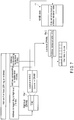
- FIG. 1 schematically shows an SSD 11 to which the embodiment is applied.
- the SSD 11 comprises, for example, a host interface (host I/F) 12 , a front end 13 , a back end 14 , a DRAM 15 contained in, for example, the back end 14 , a NAND controller 16 , a NAND 17 and a power supply 18 .
- host I/F host interface
- the host interface (hereinafter, the host I/F) 12 comprises a serial attached SCSI (SAS) interface, a serial advanced technology attachment (SATA) interface, or the like.
- SAS serial attached SCSI
- SATA serial advanced technology attachment
- the SSD 11 is connected to a host 21 , such as a personal computer, via the host I/F 12 , and functions as an external memory for the host 21 .
- the host 21 When issuing a read command or a write command as a host IF command to the SSD 11 , the host 21 issues a command including a logical block address (LBA) as a logical address.
- LBA logical block address
- the SSD 11 receives, from the host 21 , the command to read or write user data designated by the logical address.
- the SSD 11 transmits user data, stored in the NAND 17 , to the host 21 via a read buffer (not shown).
- the SSD 11 stores user data received from the host 21 in the NAND 17 via a write buffer (not shown).
- the front end 13 performs receive/transmit processing of host I/F commands to receive and transmit data from and to the host 21 via the host I/F 12 .
- the front end 13 comprises, for example, a CPU 13 a and a command queue 13 b , and mainly processes the host IF commands.
- the function of the front end 13 is realized by software (firmware) executed in the CPU 13 a.
- the command queue 13 b has a queue structure capable of buffering a plurality of commands, and is configured to receive a host IF command from the host 21 , and to transfer the command to the back end 14 if the command corresponds to a user data read or write command.
- the CPU 13 a of the front end 13 cooperates with the CPU 14 a of the back end 14 to transfer data between the write buffer and the host 21 and between the read buffer and the host 21 .
- the back end 14 comprises, for example, the above-mentioned CPU 14 a , a command queue 14 b , a write buffer (not shown), a read buffer (not shown) and the above-mentioned DRAM 15 .
- the function of the back end 14 is realized by firmware executed on the CPU 14 a .
- the back end 14 functions as a controller configured to translate host IF commands into commands corresponding to the NAND 17 to thereby execute various types of processing.
- the back end 14 executes, for example, the following processing:
- the DRAM 15 stores, for example, an address translation table 15 a , a logical and physical block table 15 b and a defect in physical block table 15 c .
- the address translation table 15 a shows the correspondence between the LBA supplied as the logical address from the host 21 , and the data position (block address+page address in each block) recorded in the NAND 17 .
- the logical and physical block table 15 b shows the correspondence between a logical block and a physical block group constituting the logical block, as described later.
- the physical block table 15 c shows defective portions of bit groups stored in the NAND 17 . Defective portions may be referred to as defective positions in the specification.
- the DRAM 15 is a memory to which the supply of power can be partially shut off by, for example, limiting a range to be refreshed.
- the DRAM 15 is managed by the CPU 14 a .
- the address translation table 15 a , the logical and physical block table 15 b and the physical block table 15 c are normally stored in the NAND 17 , and are read therefrom and expanded in the DRAM 23 on boot.
- the address translation table 15 a and the logical and physical block table 15 b in the DRAM 15 are saved and stored in the NAND regularly or at the time of power off. However, it is not necessary to always expand the entire address translation table 15 a and logical and physical block table 15 b in the DRAM 15 , but may be read from the NAND 17 when necessary.
- the DRAM 15 will be described later in detail.
- the command queue 14 b has a queue structure capable of accumulating a plurality of commands, and translates an LBA in a command received from the front end 13 into a physical address in the NAND 17 , using the address translation table 15 a in the DRAM 15 . Read or write commands including the physical addresses are supplied to the NAND controller 16 .
- the NAND controller 16 controls a data write and a data read to and from the NAND 17 , based on commands issued by the back end 14 .
- the NAND 17 comprises a memory cell array having a plurality of memory cells arranged in a matrix. Each memory cell can store multi-level data using an upper page and a lower page. Data write and read are performed on a page basis.
- the NAND 17 is formed of a plurality of blocks, each block including a plurality of pages. The block is an erasing unit of data. Further, each page is formed of a plurality of data sectors. One sector is a minimum unit of access by the host. The size of a sector is, for example, 512 bytes.
- the power supply 18 is formed of, for example, a rechargeable battery as a backup power supply, or of a capacitor.
- the power supply 18 supplies power to, for example, part of the DRAM 15 when power loss occurs, described later.
- FIG. 2 shows an example of the DRAM 15 .
- the DRAM 15 is a memory that can be partially powered off. More specifically, the DRAM 15 has a partial array self refresh (PASR) function that enables selective refresh of, for example, a half or quarter area of the entire DRAM 15 from, for example, the lower address.
- PASR partial array self refresh
- the supply of power to the DRAM 15 is shut off when there is no request to read or write user data from the host for a predetermined period of time. More specifically, in the following two cases, power is shut off.
- a first case is where the back end 14 , for example, detects that the host 21 has not issued a read or write request for three seconds.
- a second case is where the host 21 explicitly requests the SSD 11 to transit to the low-power state. In these cases, the supply of power to the half area or three quarter area of the DRAM 15 is shut off. At this time, however, the power supply to the remaining half or quarter area of the DRAM 15 is continued, and therefore the data held in these areas is maintained as it is.
- FIG. 2 shows a case where the power supply to the half area of the DRAM 15 is shut off.
- a first area 15 - 1 indicates an area where power is supplied, and a second area 15 - 2 indicates an area where power can be shut off. Accordingly, data, such as the address translation table 15 a and the logical and physical block table 15 b , needed for quick response to a request from the host 21 is held in the area 15 - 1 to which power is supplied.
- the configuration of the SSD 11 is not limited to that of FIG. 1 .
- the NAND controller 16 and the back end 14 may be integrated, while the DRAM 15 may be formed separate from the back end 14 .
- the volatile memory is not limited to the DRAM 15 , but may be, for example, an SRAM.
- the nonvolatile memory is not limited to the NAND 17 .
- FIG. 3 shows the operation of the back end 14 performed when the host 21 has issued a user data read request.
- the address translation table 15 a translates a logical address supplied from the host 21 into a physical address indicative of a position in the NAND 17 .
- each entry of the address translation table 15 a is constituted of a physical address corresponding to a logical address.
- An upper address in an address obtained after translation indicates a physical block in the NAND 17
- a lower address in the address indicates a physical address in the physical block.
- a set of physical blocks is called a logical block.
- a logical NAND block address (which is a logical block address in the NAND and differs from a logical address from the host) indicating a set of physical blocks is output.
- the logical and physical block table 15 b indicates the correspondence between a logical block and a group of physical blocks constituting the logical block.
- each entry of the logical and physical block table 15 b is made to correspond to a corresponding logical block address, and is constituted of data indicative of the number of valid user data clusters and a physical block structure.
- the physical block structure indicates a NAND physical block group (hereinafter, also referred to simply as NAND blocks), and the number of valid clusters indicates the amount of valid user data in the NAND block group, i.e., the total number of clusters to be referred to by the address translation table 15 a .
- the cluster means a minimum unit to access to the NAND. Referring to the logical and physical block table 15 b , physical blocks in the NAND 17 can be determined based on a logical block.
- the NAND 17 includes defective portions in a bit group of the NAND block, from or to which a data read or a data write is impossible. When accessing the NAND 17 , the defective portions should be avoided.
- the physical block table 15 c shown in FIG. 3 stores addresses assigned to the defective portions of the NAND 17 , and is configured to extract defective portions corresponding to physical blocks indicated by the logical and physical block table 15 b . This enables defective portions to be corrected to generate user data clusters, when data is read from the NAND 17 in response to, for example, a read request from the host 21 . More specifically, when, for example, user data is written, it is written to a cluster avoiding the defective portions.
- data when data is read from the NAND 17 in response to a read request output from the host 21 , it is read from a group of bits that are free from the defective portions, is then reconstructed based on the data in the physical block table 15 c , and is transmitted as user data to the host 21 .
- the host 21 If the host 21 requests a write to an area of a single logical address a number of times, the last written user data becomes valid and the other data becomes invalid.
- writes associated with a single logical address in the NAND 17 are performed not by overwriting an area of a single physical address, but by performing writes to areas of different physical addresses.
- the address translation table 15 a is updated such that a physical address, to the area with which a last write is made, is set to correspond to the logical address. Namely, the address translation table 15 a does not show the physical address associated with the user data other than the last written user. This means that the user data other than the last written one becomes invalid.
- a cluster As a unit for indicating whether user data is valid or invalid, a cluster as a minimum unit for writing to the NAND is used. Namely, to be valid or invalid is determined per cluster.
- One cluster is formed of data corresponding to, for example, 8 logical addresses. For instance, if data corresponding to one logical address is of 512 bytes, one cluster is of 4096 bytes.
- each NAND block In order to determine how many valid clusters are included in each NAND block, by referring to the address translation table in the NAND 17 , it is necessary to determine whether each cluster in each NAND block is valid. This processing requires a lot of time. In view of this, when a write request is issued from the host 21 , or when garbage collection is performed, the number of valid clusters is figured out, and the number of valid clusters in the logical and physical block table is updated along with the update of the address translation table, as will be described later.
- the address translation table 15 a and the logical and physical block table 15 b of the back end 14 are updated, when necessary, based on the address translation table and the logical and physical block table of the NAND 17 .
- the address translation table 15 a may be layered. Firstly, a high level of a hierarchical structure is searched for, using the upper address of a logical address, and a low level of the hierarchical structure is searched for, using the search result of the high level and the lower address of the logical address.
- a high level of a hierarchical structure is searched for, using the upper address of a logical address
- a low level of the hierarchical structure is searched for, using the search result of the high level and the lower address of the logical address.
- FIG. 7 shows the correspondence relationship between each logical address and the address translation table 15 a .
- the address translation table 15 a comprises a high level 15 a - 1 and a low level 15 a - 2 .
- the upper address of each logical address corresponds to the high level 15 a - 1
- the lower address of the same corresponds to the low level 15 a - 2 .
- the upper 19 bits are made to correspond to the high level 15 a - 1 of the address translation table 15 a
- the middle 10 bits are made to correspond to the low level 15 a - 2 of the address translation table 15 a
- the lower 3 bits are made to indicate which 512-byte data in a cluster corresponds to the logical address.
- Each entry of the high level 15 a - 1 includes data indicative of a location (physical address) in the NAND 17 , and data indicative of the location of the low level 15 a - 2 in the DRAM 15 . Further, each entry of the low level 15 a - 2 includes data indicative of a physical address in a NAND block corresponding to the middle bit address of the logical address.
- FIG. 7 shows a case where both the high and low levels 15 a - 1 and 15 a - 2 are stored in the DRAM 15 , the low level 15 a - 2 may not be stored in the DRAM 15 , depending upon circumstances.
- Data other than user data i.e., the address translation table 15 a , the logical and physical block table 15 b , the physical block table 15 c and other management data (hereinafter, these are collectively referred to as “metadata”) are also stored in the NAND 17 .
- the metadata is appended to the NAND 17 , like the user data. Accordingly, blocks storing the metadata are also managed.
- the metadata may be stored in, for example, a logical block, like user data.
- the metadata ( 31 ) may be stored in a physical block in the NAND 17 without using the logical and physical block table 15 b , as is shown in FIG. 8 .
- Each logical address is of 32 bits, is divided as mentioned above, and is made to correspond to the address translation table 15 a .
- a group of entries of the low level corresponding to one entry of the high level in the address translation table 15 a is written and read as one cluster to and from the NAND 17 .
- a plurality of groups of entries may be collectively treated as one cluster. In the latter case, the position in the NAND, in which the low level is stored, indicates the position in the cluster indicated by the lower bits of the logical address, like user data.
- the size of the high level of the address translation table 15 a needed for reading user data corresponding to one logical address corresponds to one cluster (4 Kbytes).
- the size of the low level for the same purpose is 2 31 (2 Gbytes).
- the total size of the high level of the address translation table 15 a is 2 21 (2 Mbytes). From this, it is evident that there is a great difference between the entire capacity of the address translation table 15 a and the capacity of the DRAM 15 needed for reading user data once.
- the high level of the address translation table 15 a is not held in the DRAM 15 but is read from the NAND 17 . To this end, it is necessary to read a plurality of the low levels which are appended to the NAND 17 , beginning from one which is lastly written to the NAND 17 , thereby detecting newest one.
- a defective portion may cover a plurality of write units, e.g., clusters or pages.
- information associated with the defective portion can be stored in a unit greater than a cluster. Assume here that 16 clusters have respective defective portions of the same position.
- the capacity of the DRAM 15 that is required at a time can be suppressed by layering the physical block table 15 c , like the address translation table 15 a.
- the physical block table 15 c of the uppermost layer which has been subjected to error correction and hence has no errors, is developed in the DRAM 15 .
- the physical block table 15 c is read from the NAND 17 , it is read with detective portions avoided, thereby acquiring user data to access or defective portions of metadata.
- the number of times of reading the physical block table 15 c from the NAND 17 becomes twice.
- the DRAM 15 has a storage capacity of 1 Mbytes, it can hold all content of the high level of the physical block table 15 c .
- FIG. 9 shows an example of the layered physical block table 15 c in the DRAM 15 .
- the physical block table 15 c comprises a high level 15 c - 1 , a plurality of middle levels 15 c - 2 , and a plurality of low levels 15 c - 3 .
- an entry of the high level 15 c - 1 is searched for.
- an entry of the middle level 15 c - 2 is searched for, and using the lower 9 bits, an entry of the low level 15 c - 3 is searched for.
- the entries of the high level 15 c - 1 indicate record positions of the NAND 17 in which the middle levels are recorded, also hold defective portions in the NAND 17 that store the middle levels, and hold the positions in the DRAM 15 that hold the middle levels.
- the respective middle levels 15 c - 2 are read from the NAND 17 storing the middle levels, and are corrected based on defective portions 15 c - 1 in the NAND 17 storing the middle levels.
- the corrected middle levels are supplied and held in the middle levels 15 - 2 .
- the respective entries of the middle levels 15 c - 2 indicate the record positions of the NAND 17 in which the low levels are stored.
- the middle levels 15 c - 2 hold the defective portions of the NAND 17 in which the low levels are stored, and also hold the holding positions of the DRAM 15 in which the low levels are held.
- the respective low levels 15 c - 3 are read from the NAND 17 that stores the low levels, and are corrected based on the defective portions of the NAND 17 storing the low levels.
- the corrected low levels are supplied to and held in the low levels 15 c - 3 .
- the respective low levels 15 c - 3 Upon receiving the physical block addresses of the low level, the respective low levels 15 c - 3 output defective portions of target physical blocks in the NAND 17 .
- the high level 15 c - 1 in the physical block table 15 c must be always stored in the DRAM 15 .
- the middle levels 15 c - 2 and the low levels 15 c - 3 may be stored in the DRAM 15 only when necessary.
- the high level 15 c - 1 in the physical block table 15 c is read from the NAND 17 and held in the DRAM 15 .
- a middle level 15 c - 2 of the physical block table 15 c is read from NAND 17 and held in the DRAM 15 .
- a low level 15 c - 3 of the physical block table 15 c is read from the NAND 17 and held in the DRAM 15 .
- data is read from a physical block of the NAND 17 storing user data.
- the physical block table 15 c shown in FIG. 9 comprises the high level 15 c - 1 , the middle levels 15 c - 2 and the low levels 15 c - 3 , the embodiment is not limited to this, but may be modified such that the table has a two-layer structure of high and low levels.
- the embodiment can reduce the power supplied to the DRAM 15 by optimizing data held on the DRAM 15 .
- the DRAM 15 has a function called PASR, and can selectively turn off power by selecting the range of refresh during operation of the DRAM 15 . If there is no user data read or write from the host 21 for a predetermined period of time, the power to the DRAM 15 is turned off. More specifically, if the back end 14 detects that there is no read or write request from the host 21 for a predetermined period of time (e.g., three seconds), or if an explicit request to set the SSD in a low-power state is issued from the host 21 , the back end 14 partially cuts the supply of power to the DRAM 15 . Thus, the supply of power to the DRAM 15 is partially cut to reduce its power consumption.
- a predetermined period of time e.g., three seconds
- FIG. 10 shows the relationship between the refresh range (indicated by the arrows) in the DRAM 15 that is in a low-power state, and the storage content. More specifically, in a normal power consumption state, the entire area of the DRAM 15 is refreshed and data have been held. In contrast, in the low-power state, in the DRAM 15 , for example, only a half or quarter address space from the lower address is refreshed. Whether the half or quarter address space is refreshed depends upon a required power consumption. Thus, the capacity of data holding of the DRAM 15 is reduced compared to the normal power consumption state.
- the data which needs to scan the NAND 17 in order to access the data is proportional to a capacity of the NAND 17 , or longer than it. If such data is needed for user data reading or writing, response to the host 21 is impossible within a limited time (for example, 2 seconds) required by the host 21 . To avoid this, such data is held in the DRAM 15 .
- the data that must be held in the DRAM 15 includes the high level (the record positions of the low levels in the NAND 17 , and the hold positions of the DRAM 15 ) of the address translation table 15 a , the logical and physical block table 15 b and the number of valid clusters of a logical address, and the high level 15 c - 1 of the physical block table 15 c in the NAND 17 (the record positions of the middle levels in the NAND 17 , the hold positions of the middle levels in the DRAM 15 , the defective portions of the NAND area storing the middle levels), as is shown in FIG. 10 .
- the content of the high level 15 c - 1 includes the record positions of the low levels in the NAND 17 , the hold positions of the low levels in the DRAM, and the defective portions of the NAND area storing the low levels.
- the area supplied with power will have a free area, if only the above-mentioned data is held therein.
- priorities may be assigned to other data, and data having higher priorities may be held in the free area supplied with power.
- data of the highest priority is defective portions in the NAND 17 that store the address translation table 15 a .
- the data having second higher priority is a low level table with high priority included in a group of low level tables of the address translation table 15 a , or defective portions in the NAND 17 which store user data.
- Higher priorities are assigned to the most recently used address translation table 15 a and the most recently used physical block table of the NAND 17 .
- Data of higher priorities is held as long as possible in the area of the DRAM 15 always supplied with power, while data of lower priorities is held in accordance with the ratio of a free area in the area of the DRAM 15 supplied with power. If there is no free area, the data is not held in the DRAM 15 , and is read from the NAND 17 when necessary.
- a higher priority is assigned to an address that has a stronger possibility of being read next. For instance, based on a temporal locality that a logical address recently used for reading or writing may be accessed again, a priority is assigned utilizing an algorithm, such as least recently used (LRU). Alternatively, priority assignment can be done based on a spatial locality that a logical address subsequent to a recently read logical address may be read soon.
- LRU least recently used
- FIFO first in first out
- FIG. 11 shows an example of a FIFO structure, in which the low level of the address translation table 15 a is held in the DRAM 15 .
- a highest priority is assigned to the entry (S 1 ), and the entries of the priorities other than the entry of the highest priority are lowered to priority (S 2 ).
- S 3 the entry held in the DRAM 15 is used, it is set to a highest priority (S 3 ). If the DRAM 15 has no area for holding an entry, an entry of the lowest priority is removed from the DRAM 15 (S 4 ).
- a hint that a logical address will be used for reading or writing in near future may be imparted in accordance with a read or write request from the host 21 , and the priority may be determined based on the hint.
- defective portions corresponding to the storage area of the NAND 17 that records an address translation table may be held in the area 15 - 1 of the DRAM 15 in preference to defective portions corresponding to the storage area of the NAND 17 that stores user data.
- three types of data such as the data of the high level of the address translation table 15 a having a highest priority, the number of valid clusters of each logical block of the logical and physical block table 15 b , and the high level content of the defective portions of the NAND 17 , are held in the DRAM 15 .
- the low levels of the address translation table 15 a are referred to for reading user data, it is necessary to access the NAND 17 only for the user data, and it is not necessary to access the NAND for the three types of data, i.e., the data of the high level of the address translation table 15 a having the highest priority and held in the DRAM 15 , the number of valid clusters of each logical block of the logical and physical block table 15 b , and the high level content of the defective portions of the NAND 17 . Further, the defective portions of the NAND 17 that store the address translation table and have an intermediate priority are needed to be read from the NAND 17 once. Furthermore, in order to read the defective portions of the NAND 17 that store the address translation table 15 a as data of the lowest priority and user data from the NAND 17 , twice reads are required.
- the holding of the address translation table 15 a and the defective portions based on the priority will now be described in view of the memory functions.
- the area of the DRAM 15 always supplied with power is set smaller than the other area to which the supply of power is shut off.
- the area of the DRAM 15 always supplied with power holds data of higher priorities, and the area, the supply of power to which is shut off, holds data of lower priorities.
- the data of lower priorities is read from the NAND 17 whenever it is needed, because the NAND 17 has a longer latency and a greater capacity than the DRAM 15 .
- a volatile memory for temporarily holding data such as a static RAM (SRAM), may be added, as well as the DRAM 15 .
- SRAM static RAM
- FIG. 12 schematically shows the memory structure assumed when an SRAM is added.
- an SRAM 41 as a memory of a low latency and a small capacity is provided, and the area of the DRAM 15 always supplied with power and the area of the DRAM 15 , the supply of power to which is shut off, are provided in this order as the latency and capacity are increased.
- the NAND 17 as a memory of a high latency and a large capacity is provided.
- Data as reference and to-be-updated data is transferred from the NAND 17 to the SRAM 41 via the DRAM 15 , and updated data is written to the SRAM 41 , the DRAM 15 and the NAND 17 in this order.
- data of the highest priority is held in the SRAM 41
- data of lower priorities are held in the DRAM 15 and the NAND 17 .
- the above processing is executed in accordance with user data read or write based on garbage collection or a request from the host 21 .
- positions are not fixed during normal reading or writing where in the DRAM 15 data should be located, and when the host 21 has requested a transition to the low-power state, the data in the DRAM 15 is rearranged in accordance with the priorities.
- the back end 14 collects data of higher priorities in the area of the DRAM 15 always supplied with power. The data in the other area of the DRAM 15 will be lost when power is shut off.
- a write to the NAND 17 is executed in accordance with a predetermined procedure determined by the back end 14 , regardless of the logical address. Accordingly, it is beforehand known that subsequent data is written to a subsequent plane (i.e., an area including a plurality of physical blocks in a memory cell array) or a subsequent page of the lastly written one of the NAND. Therefore, by holding defective portions of a plane or page as a write destination in a nonvolatile memory, processing of reading defective portions as write destinations from the NAND 17 can be omitted. As a result, a response time to a write request from the host 21 can be shortened, even if the request occurs during a low-power operation.
- FIG. 13 shows an example of an operation of the back end 14 performed at the time of transition to the low-power state.
- the address translation table 15 a in the DRAM 15 is updated to indicate the position of the user data in the NAND 17 (S 13 ). Namely, the high and low levels of the address translation table 15 a are updated.
- the high level of the address translation table 15 a is held in the area of the DRAM 15 supplied with power during a transition to the low-power state, and is therefore not stored in the NAND 17 .
- the high level of the address translation table 15 a is updated to indicate the position of the NAND 17 in which the low level is stored (S 15 ).
- step S 14 If in step S 14 , the high level is written to the NAND 17 whenever a transition to the low-power state occurs, a write amplification factor (WAF) indicative of how many times the amount of data actually written to the NAND 17 compared with the amount of data supplied from the host 21 is will increase, which is inconvenient.
- WAF write amplification factor
- changed data is stored in the NAND 17 from the low levels to the high level in order, and the physical block table 15 c is updated so as to indicate a position in the NAND 17 in a higher level by one stage.
- FIG. 14 shows an example of an operation of the back end 14 performed when the device is returned from the above-mentioned low-power state.
- the host 21 When, for example, the host 21 explicitly requests the SSD 11 to be returned from the low-power state, the supply of power to the area of the DRAM 15 , to which the supply of power was shut off, is resumed. In this state, the back end 14 firstly reads a low level of the address translation table 15 a from the NAND 17 (S 21 ). This processing is performed in parallel with processing in steps S 22 to S 25 , except for determination processing in step S 26 described later.
- a user data read request has been issued from the host 21 (S 22 ). If it is determined that the user data read request has been issued, it is determined whether the address translation table 15 a associated with the user data is already read from the NAND 17 (S 23 ). Namely, it is determined whether the address translation table 15 a in the DRAM 15 includes a low level corresponding to the requested user data has been requested. If there is no low level corresponding to the requested user data, the low level corresponding to the requested user data is read from the NAND 17 in preference to the other low levels (S 24 ).
- step S 23 If in step S 23 , it is determined that the low level corresponding to the requested user data is already read, or if in step S 24 , the low level corresponding to the requested user data has been read, the requested user data is read from the NAND 17 using the address translation table 15 a (S 25 ).
- step S 26 it is determined whether all of the low levels of the address translation table 15 a have been read from the NAND 17 (S 26 ). If it is determined that all of the low levels have not been read, control is transited to step S 21 , where the above-described operations are iterated. In contrast, if it is determined that all of the low levels of the address translation table 15 a have been read, the user data read in step S 25 is transferred to the host 21 .
- FIG. 15 schematically shows the operations performed to reconstruct the high level of the address translation table 15 a .
- the high level of the address translation table 15 a can be reconstructed in the DRAM 15 by reading a plurality of low levels from the NAND 17 .
- the high level of the address translation table 15 a includes a plurality of low level entries. Each entry comprises a record position in the NAND 17 and a hold position in the DRAM 15 .
- the record position in the NAND 17 indicates a physical address assigned to a position in the NAND 17 , to which a low level of the address translation table is written.
- each low level in the address translation table 15 a is appended to the NAND 17 whenever the table is updated. Accordingly, in association with, for example, a low level B or a low level C in the address translation table shown in FIG. 15 , the table (newest table) lastly written to the NAND 17 is valid, and the table (not the newest table) written before the last table is invalid.
- FIG. 15 it is checked in which order the low levels of each address translation table were written to the NAND 17 , and the physical address of a corresponding newest low level in the NAND 17 is held in a corresponding entry of the high level in the DRAM 15 , thereby constituting the high level. Subsequently, in accordance with data in each entry of the thus-constituted high level, data of low level is read from the NAND 17 , and is held in the DRAM 15 .
- middle levels are provided as in the physical block table 15 c , they are constructed from the low levels, and the high level is constructed from the middle levels.
- step S 26 of FIG. 14 if it is determined in step S 26 of FIG. 14 that all the low levels of the address translation tables 15 a are not yet read from the NAND 17 , it is optional to read all low level tables from the NAND 17 . For instance, if it is judged that to reduce power consumption, it is not necessary to read all low level tables from the NAND 17 , or if the power state is again transited to the low-power state, reading of the low level tables can be stopped.
- FIG. 14 shows the operation performed when the low levels of the address translation table 15 a are restored
- the same operation as the above is also performed to restore each physical block table 15 c of the NAND 17 .
- the host 21 has issued a request to read, for example, user data
- a physical block table necessary for this read request is read from the NAND 17 before the other physical block tables are read, thereby constructing the corresponding physical block table 15 c .
- the high level 15 c - 1 of a physical block table 15 c is read from the NAND 17 based on the held position of the high level held in the DRAM 15 .
- middle levels 15 c - 2 and low levels 15 c - 3 are read from the NAND 17 , thereby constituting the physical block table 15 c.
- a low level address translation table 15 a needed for the write request, and a corresponding physical block table of the NAND 17 are read from the NAND 17 in preference to the other data, as in the case of read request mentioned above.
- defective portions of a block to which the user data requested to be written by the host 21 is to be written, defective portions of a block to which the user data to be moved for garbage collection is to be written, and defective portions of a block to which the address translation table 15 a is to be written, are held in the area 15 - 1 of the DRAM 15 to which power is supplied.
- the above-mentioned processing performed in the low-power state is also applicable to power loss processing.
- power loss processing is performed. In power loss processing, it is necessary to make user data nonvolatile, which is not yet written the user data to NAND 17 although a response indicative of that a write of the user data to the host 21 has been completed is returned. To shorten the time required for writing the user data to the NAND 17 , a dedicated block for writing data using a data structure different from a normal data structure is prepared, and the user data is written to this block. The data stored in the dedicated block is reflected in the normal data structure for the next activation.
- a logical and physical block table and a physical block table associated with the dedicated block are always held in the DRAM 15 .
- no physical block table is read from the NAND 17 when power loss has occurred, with the result that the time required for power loss processing can be shortened by, for example, 1 msec.
- the device is transited to the low-power state. This means that progress of the garbage collection must be held.
- the data held as the halfway progress indicates defective portions in source and destination blocks, the address translation table 15 a for determining whether each cluster in the source blocks is valid, and a set of valid clusters determined to be written to the destination blocks.
- the high level of the address translation table 15 a when the device is transited to the low-power state, the high level of the address translation table 15 a , the number of valid clusters in the logical blocks of the logical and physical block table 15 b , and the high level of the physical block table 15 c are held in the area of the DRAM 15 supplied with power. This reduces the amount of data read from the NAND 17 when the device is returned from the low-power state. Therefore, it is possible to decrease the response time to the host 21 .
- the data held in the DRAM 15 is set necessary minimum in order to increase the speed of response to the host 21 .
- the area of the DRAM 15 supplied with power can be reduced, and hence the consumption of power can be reduced.
- FIG. 16 shows processing performed when the supply of power to the DRAM 15 is not shut off, i.e., when low-power control is not performed, and processing performed when the supply of power to the DRAM 15 is completely shut off.
- elements similar to those shown in FIGS. 13 and 14 are denoted by corresponding reference numbers.
- marks “•” indicate the cases where respective processes are performed.
- steps S 13 to S 15 of the embodiment are not needed for a transition to the low-power state, and when the device is restored from the low-power state, processing in steps S 21 to S 26 of the embodiment is not needed. Accordingly, the time required for return from the low-power state is shorter than in the embodiment, and the consumption of power is greater than in the embodiment.
- the consumption of power is less than the embodiment when the power to the DRAM 15 is completely shut off.
- writing the high level of the address translation table, as shown in Ti is additionally needed when the device is transited to the low-power state, compared to the embodiment.
- reading the high level of the address translation table 15 a from the NAND 17 as shown in T 4 or a step of reconstructing the high level of the address translation table 15 a is additionally needed, compared to the embodiment. This requires a longer time for the return from the low-power state, than in the embodiment, which makes it difficult to quickly respond to the host 21 .
- the power required for it can be reduced, while when the device is returned from the low-power state, it can quickly respond to the host 21 .
Landscapes
- Engineering & Computer Science (AREA)
- Theoretical Computer Science (AREA)
- Human Computer Interaction (AREA)
- Physics & Mathematics (AREA)
- General Engineering & Computer Science (AREA)
- General Physics & Mathematics (AREA)
- Memory System (AREA)
- Techniques For Improving Reliability Of Storages (AREA)
Abstract
Description
-
- Responses to various commands, such as a write command and a read command, from the
host 21 - Reading and writing of user data by garbage collection for compacting of invalid areas in the
NAND 17 - Translation of a logical address from the
host 21 into a physical address in theNAND 17 - Update of the address translation table, a logical and physical block table, etc.
- Processing of storing the tables in the
NAND 17 to perpetuate them and to make them nonvolatile data - Management of a physical block table showing defective portions of physical block portions
- Management of the number of valid clusters in a logical block
- Responses to various commands, such as a write command and a read command, from the
Claims (42)
Priority Applications (1)
| Application Number | Priority Date | Filing Date | Title |
|---|---|---|---|
| US14/641,099 US10747449B2 (en) | 2014-07-31 | 2015-03-06 | Reduction of power use during address translation via selective refresh operations |
Applications Claiming Priority (2)
| Application Number | Priority Date | Filing Date | Title |
|---|---|---|---|
| US201462031185P | 2014-07-31 | 2014-07-31 | |
| US14/641,099 US10747449B2 (en) | 2014-07-31 | 2015-03-06 | Reduction of power use during address translation via selective refresh operations |
Publications (2)
| Publication Number | Publication Date |
|---|---|
| US20160034221A1 US20160034221A1 (en) | 2016-02-04 |
| US10747449B2 true US10747449B2 (en) | 2020-08-18 |
Family
ID=55180075
Family Applications (1)
| Application Number | Title | Priority Date | Filing Date |
|---|---|---|---|
| US14/641,099 Active 2036-01-01 US10747449B2 (en) | 2014-07-31 | 2015-03-06 | Reduction of power use during address translation via selective refresh operations |
Country Status (1)
| Country | Link |
|---|---|
| US (1) | US10747449B2 (en) |
Families Citing this family (14)
| Publication number | Priority date | Publication date | Assignee | Title |
|---|---|---|---|---|
| US9542118B1 (en) | 2014-09-09 | 2017-01-10 | Radian Memory Systems, Inc. | Expositive flash memory control |
| JP6609199B2 (en) * | 2016-03-01 | 2019-11-20 | ルネサスエレクトロニクス株式会社 | Embedded equipment |
| WO2018057039A1 (en) * | 2016-09-26 | 2018-03-29 | Hewlett-Packard Development Company, L. | Update memory management information to boot an electronic device from a reduced power mode |
| JP6732684B2 (en) * | 2017-03-15 | 2020-07-29 | キオクシア株式会社 | Information processing device, storage device, and information processing system |
| KR20190052441A (en) * | 2017-11-08 | 2019-05-16 | 에스케이하이닉스 주식회사 | Memory controller and method for operating the same |
| US11262921B2 (en) | 2017-12-21 | 2022-03-01 | Qualcomm Incorporated | Partial area self refresh mode |
| KR102528258B1 (en) * | 2018-04-30 | 2023-05-04 | 에스케이하이닉스 주식회사 | Memory controller and operating method thereof |
| US11175984B1 (en) | 2019-12-09 | 2021-11-16 | Radian Memory Systems, Inc. | Erasure coding techniques for flash memory |
| KR102848954B1 (en) | 2020-02-28 | 2025-08-20 | 삼성전자주식회사 | Storage device and Method of operating the storage device |
| US11586385B1 (en) | 2020-05-06 | 2023-02-21 | Radian Memory Systems, Inc. | Techniques for managing writes in nonvolatile memory |
| US20220083252A1 (en) * | 2020-09-14 | 2022-03-17 | Micron Technology, Inc. | Indication-based avoidance of defective memory cells |
| US11763040B2 (en) | 2021-04-07 | 2023-09-19 | Western Digital Technologies, Inc. | Enhanced D3-cold and faster recovery |
| JP7717504B2 (en) * | 2021-06-17 | 2025-08-04 | キオクシア株式会社 | Memory system and information processing system |
| JP2023040578A (en) * | 2021-09-10 | 2023-03-23 | キオクシア株式会社 | Memory system and control method |
Citations (10)
| Publication number | Priority date | Publication date | Assignee | Title |
|---|---|---|---|---|
| JPH04259989A (en) | 1991-02-15 | 1992-09-16 | Fujitsu Ltd | Power control method |
| JP2006302466A (en) | 2005-04-25 | 2006-11-02 | Elpida Memory Inc | Semiconductor storage device |
| US20090198952A1 (en) * | 2008-02-04 | 2009-08-06 | Apple Inc | Memory Mapping Architecture |
| US20110238928A1 (en) | 2010-03-25 | 2011-09-29 | Kabushiki Kaisha Toshiba | Memory system |
| JP2011192212A (en) | 2010-03-16 | 2011-09-29 | Toshiba Corp | Memory system |
| US8200885B2 (en) | 2007-07-25 | 2012-06-12 | Agiga Tech Inc. | Hybrid memory system with backup power source and multiple backup an restore methodology |
| US20130166932A1 (en) | 2011-12-22 | 2013-06-27 | Sandisk Technologies Inc. | Systems and methods of exiting hibernation in response to a triggering event |
| US20130290759A1 (en) | 2011-12-13 | 2013-10-31 | Mohan J. Kumar | Enhanced system sleep state support in servers using non-volatile random access memory |
| US20140181558A1 (en) * | 2012-12-22 | 2014-06-26 | Qualcomm Incorporated | Reducing power consumption of volatile memory via use of non-volatile memory |
| US20140195837A1 (en) * | 2013-01-08 | 2014-07-10 | Qualcomm Incorporated | Enhanced dynamic memory management with intelligent current/power consumption minimization |
-
2015
- 2015-03-06 US US14/641,099 patent/US10747449B2/en active Active
Patent Citations (13)
| Publication number | Priority date | Publication date | Assignee | Title |
|---|---|---|---|---|
| JPH04259989A (en) | 1991-02-15 | 1992-09-16 | Fujitsu Ltd | Power control method |
| JP2006302466A (en) | 2005-04-25 | 2006-11-02 | Elpida Memory Inc | Semiconductor storage device |
| US7333363B2 (en) | 2005-04-25 | 2008-02-19 | Elpida Memory, Inc. | Semiconductor storage apparatus |
| US8200885B2 (en) | 2007-07-25 | 2012-06-12 | Agiga Tech Inc. | Hybrid memory system with backup power source and multiple backup an restore methodology |
| US20090198952A1 (en) * | 2008-02-04 | 2009-08-06 | Apple Inc | Memory Mapping Architecture |
| US8473760B2 (en) | 2010-03-16 | 2013-06-25 | Kabushiki Kaisha Toshiba | Memory system and server system |
| JP2011192212A (en) | 2010-03-16 | 2011-09-29 | Toshiba Corp | Memory system |
| JP2011203905A (en) | 2010-03-25 | 2011-10-13 | Toshiba Corp | Memory system |
| US20110238928A1 (en) | 2010-03-25 | 2011-09-29 | Kabushiki Kaisha Toshiba | Memory system |
| US20130290759A1 (en) | 2011-12-13 | 2013-10-31 | Mohan J. Kumar | Enhanced system sleep state support in servers using non-volatile random access memory |
| US20130166932A1 (en) | 2011-12-22 | 2013-06-27 | Sandisk Technologies Inc. | Systems and methods of exiting hibernation in response to a triggering event |
| US20140181558A1 (en) * | 2012-12-22 | 2014-06-26 | Qualcomm Incorporated | Reducing power consumption of volatile memory via use of non-volatile memory |
| US20140195837A1 (en) * | 2013-01-08 | 2014-07-10 | Qualcomm Incorporated | Enhanced dynamic memory management with intelligent current/power consumption minimization |
Also Published As
| Publication number | Publication date |
|---|---|
| US20160034221A1 (en) | 2016-02-04 |
Similar Documents
| Publication | Publication Date | Title |
|---|---|---|
| US10747449B2 (en) | Reduction of power use during address translation via selective refresh operations | |
| US10761780B2 (en) | Memory system | |
| US11836354B2 (en) | Distribution of logical-to-physical address entries across multiple memory areas | |
| US8316257B2 (en) | NAND power fail recovery | |
| US9830257B1 (en) | Fast saving of data during power interruption in data storage systems | |
| US9507711B1 (en) | Hierarchical FTL mapping optimized for workload | |
| US8954694B2 (en) | Methods, data storage devices and systems for fragmented firmware table rebuild in a solid state drive | |
| US9489296B1 (en) | Methods, devices and systems for hardware-based garbage collection in solid state drives | |
| US20110283048A1 (en) | Structured mapping system for a memory device | |
| US11537512B2 (en) | Asynchronous power loss recovery for memory devices | |
| US9529537B2 (en) | Storage system and storage method | |
| US20160117112A1 (en) | Trim command processing in a solid state drive | |
| US20090327590A1 (en) | Enhanced mlc solid state device | |
| US10977189B2 (en) | Reducing forward mapping table size using hashing | |
| KR20220031490A (en) | Zoned namespace limitation mitigation using sub block mode | |
| US20140019672A1 (en) | Memory system and control method thereof | |
| US8892816B1 (en) | System and method for writing data to a memory | |
| JP2013061799A (en) | Memory device, control method for memory device and controller | |
| US11520696B2 (en) | Segregating map data among different die sets in a non-volatile memory | |
| US9465537B2 (en) | Memory system and method of controlling memory system | |
| US11714722B2 (en) | Power loss recovery for memory devices | |
| US12346594B2 (en) | Background memory scan block selection | |
| US10446252B2 (en) | Data storage device and method for data error management | |
| US11132140B1 (en) | Processing map metadata updates to reduce client I/O variability and device time to ready (TTR) | |
| US9305665B2 (en) | Memory system and method of controlling memory system |
Legal Events
| Date | Code | Title | Description |
|---|---|---|---|
| AS | Assignment |
Owner name: KABUSHIKI KAISHA TOSHIBA, JAPAN Free format text: ASSIGNMENT OF ASSIGNORS INTEREST;ASSIGNORS:ZETTSU, TATSUYA;UEKI, KATSUHIKO;KOJIMA, YOSHIHISA;AND OTHERS;SIGNING DATES FROM 20150313 TO 20150316;REEL/FRAME:035346/0231 |
|
| AS | Assignment |
Owner name: TOSHIBA MEMORY CORPORATION, JAPAN Free format text: ASSIGNMENT OF ASSIGNORS INTEREST;ASSIGNOR:KABUSHIKI KAISHA TOSHIBA;REEL/FRAME:043529/0709 Effective date: 20170628 |
|
| STPP | Information on status: patent application and granting procedure in general |
Free format text: DOCKETED NEW CASE - READY FOR EXAMINATION |
|
| STPP | Information on status: patent application and granting procedure in general |
Free format text: NON FINAL ACTION MAILED |
|
| STPP | Information on status: patent application and granting procedure in general |
Free format text: RESPONSE TO NON-FINAL OFFICE ACTION ENTERED AND FORWARDED TO EXAMINER |
|
| STPP | Information on status: patent application and granting procedure in general |
Free format text: FINAL REJECTION MAILED |
|
| STPP | Information on status: patent application and granting procedure in general |
Free format text: NOTICE OF ALLOWANCE MAILED -- APPLICATION RECEIVED IN OFFICE OF PUBLICATIONS |
|
| STPP | Information on status: patent application and granting procedure in general |
Free format text: PUBLICATIONS -- ISSUE FEE PAYMENT VERIFIED |
|
| STCF | Information on status: patent grant |
Free format text: PATENTED CASE |
|
| AS | Assignment |
Owner name: K.K. PANGEA, JAPAN Free format text: MERGER;ASSIGNOR:TOSHIBA MEMORY CORPORATION;REEL/FRAME:055659/0471 Effective date: 20180801 Owner name: TOSHIBA MEMORY CORPORATION, JAPAN Free format text: CHANGE OF NAME AND ADDRESS;ASSIGNOR:K.K. PANGEA;REEL/FRAME:055669/0401 Effective date: 20180801 Owner name: KIOXIA CORPORATION, JAPAN Free format text: CHANGE OF NAME AND ADDRESS;ASSIGNOR:TOSHIBA MEMORY CORPORATION;REEL/FRAME:055669/0001 Effective date: 20191001 |
|
| MAFP | Maintenance fee payment |
Free format text: PAYMENT OF MAINTENANCE FEE, 4TH YEAR, LARGE ENTITY (ORIGINAL EVENT CODE: M1551); ENTITY STATUS OF PATENT OWNER: LARGE ENTITY Year of fee payment: 4 |