[go: up one dir, main page]

JP6609199B2 - Embedded equipment - Google Patents

Embedded equipment Download PDF

Info

Publication number
JP6609199B2
JP6609199B2 JP2016038574A JP2016038574A JP6609199B2 JP 6609199 B2 JP6609199 B2 JP 6609199B2 JP 2016038574 A JP2016038574 A JP 2016038574A JP 2016038574 A JP2016038574 A JP 2016038574A JP 6609199 B2 JP6609199 B2 JP 6609199B2
Authority
JP
Japan
Prior art keywords
address
program
code
update
data
Prior art date
Legal status (The legal status is an assumption and is not a legal conclusion. Google has not performed a legal analysis and makes no representation as to the accuracy of the status listed.)
Active
Application number
JP2016038574A
Other languages
Japanese (ja)
Other versions
JP2017156908A (en
Inventor
匡亮 谷本
今朝巳 萩原
直幸 森田
Current Assignee (The listed assignees may be inaccurate. Google has not performed a legal analysis and makes no representation or warranty as to the accuracy of the list.)
Renesas Electronics Corp
Original Assignee
Renesas Electronics Corp
Priority date (The priority date is an assumption and is not a legal conclusion. Google has not performed a legal analysis and makes no representation as to the accuracy of the date listed.)
Filing date
Publication date
Application filed by Renesas Electronics Corp filed Critical Renesas Electronics Corp
Priority to JP2016038574A priority Critical patent/JP6609199B2/en
Priority to KR1020170025009A priority patent/KR20170102425A/en
Priority to EP17158031.9A priority patent/EP3214545B1/en
Priority to US15/445,510 priority patent/US10642596B2/en
Priority to CN201710126476.3A priority patent/CN107145362B/en
Publication of JP2017156908A publication Critical patent/JP2017156908A/en
Application granted granted Critical
Publication of JP6609199B2 publication Critical patent/JP6609199B2/en
Active legal-status Critical Current
Anticipated expiration legal-status Critical

Links

Images

Classifications

    • GPHYSICS
    • G06COMPUTING OR CALCULATING; COUNTING
    • G06FELECTRIC DIGITAL DATA PROCESSING
    • G06F8/00Arrangements for software engineering
    • G06F8/60Software deployment
    • G06F8/65Updates
    • GPHYSICS
    • G06COMPUTING OR CALCULATING; COUNTING
    • G06FELECTRIC DIGITAL DATA PROCESSING
    • G06F12/00Accessing, addressing or allocating within memory systems or architectures
    • G06F12/02Addressing or allocation; Relocation
    • G06F12/0223User address space allocation, e.g. contiguous or non contiguous base addressing
    • G06F12/023Free address space management
    • G06F12/0238Memory management in non-volatile memory, e.g. resistive RAM or ferroelectric memory
    • G06F12/0246Memory management in non-volatile memory, e.g. resistive RAM or ferroelectric memory in block erasable memory, e.g. flash memory
    • GPHYSICS
    • G06COMPUTING OR CALCULATING; COUNTING
    • G06FELECTRIC DIGITAL DATA PROCESSING
    • G06F12/00Accessing, addressing or allocating within memory systems or architectures
    • G06F12/02Addressing or allocation; Relocation
    • G06F12/0223User address space allocation, e.g. contiguous or non contiguous base addressing
    • G06F12/0292User address space allocation, e.g. contiguous or non contiguous base addressing using tables or multilevel address translation means
    • GPHYSICS
    • G06COMPUTING OR CALCULATING; COUNTING
    • G06FELECTRIC DIGITAL DATA PROCESSING
    • G06F8/00Arrangements for software engineering
    • G06F8/60Software deployment
    • G06F8/65Updates
    • G06F8/654Updates using techniques specially adapted for alterable solid state memories, e.g. for EEPROM or flash memories
    • GPHYSICS
    • G06COMPUTING OR CALCULATING; COUNTING
    • G06FELECTRIC DIGITAL DATA PROCESSING
    • G06F8/00Arrangements for software engineering
    • G06F8/60Software deployment
    • G06F8/65Updates
    • G06F8/658Incremental updates; Differential updates
    • GPHYSICS
    • G06COMPUTING OR CALCULATING; COUNTING
    • G06FELECTRIC DIGITAL DATA PROCESSING
    • G06F9/00Arrangements for program control, e.g. control units
    • G06F9/06Arrangements for program control, e.g. control units using stored programs, i.e. using an internal store of processing equipment to receive or retain programs
    • G06F9/44Arrangements for executing specific programs
    • G06F9/445Program loading or initiating
    • G06F9/44521Dynamic linking or loading; Link editing at or after load time, e.g. Java class loading
    • HELECTRICITY
    • H04ELECTRIC COMMUNICATION TECHNIQUE
    • H04LTRANSMISSION OF DIGITAL INFORMATION, e.g. TELEGRAPHIC COMMUNICATION
    • H04L67/00Network arrangements or protocols for supporting network services or applications
    • H04L67/34Network arrangements or protocols for supporting network services or applications involving the movement of software or configuration parameters 
    • GPHYSICS
    • G06COMPUTING OR CALCULATING; COUNTING
    • G06FELECTRIC DIGITAL DATA PROCESSING
    • G06F2212/00Indexing scheme relating to accessing, addressing or allocation within memory systems or architectures
    • G06F2212/25Using a specific main memory architecture
    • G06F2212/251Local memory within processor subsystem
    • GPHYSICS
    • G06COMPUTING OR CALCULATING; COUNTING
    • G06FELECTRIC DIGITAL DATA PROCESSING
    • G06F2212/00Indexing scheme relating to accessing, addressing or allocation within memory systems or architectures
    • G06F2212/72Details relating to flash memory management
    • G06F2212/7201Logical to physical mapping or translation of blocks or pages
    • GPHYSICS
    • G06COMPUTING OR CALCULATING; COUNTING
    • G06FELECTRIC DIGITAL DATA PROCESSING
    • G06F2212/00Indexing scheme relating to accessing, addressing or allocation within memory systems or architectures
    • G06F2212/72Details relating to flash memory management
    • G06F2212/7208Multiple device management, e.g. distributing data over multiple flash devices

Landscapes

  • Engineering & Computer Science (AREA)
  • Theoretical Computer Science (AREA)
  • Software Systems (AREA)
  • General Engineering & Computer Science (AREA)
  • Physics & Mathematics (AREA)
  • General Physics & Mathematics (AREA)
  • Computer Security & Cryptography (AREA)
  • Computer Networks & Wireless Communication (AREA)
  • Signal Processing (AREA)
  • Stored Programmes (AREA)
  • Memory System (AREA)

Description

本発明は組込み機器及びプログラムの更新方法に関し、例えば差分プログラムを用いた更新を行う組込み機器及びプログラムの更新方法に関する。   The present invention relates to an embedded device and a program update method, for example, an embedded device that performs an update using a differential program and a program update method.

近年、車載機器及び産業機器などに組み込まれる組込み機器が増加している。そして、このような組込み機器におけるプログラムをいわゆるOTA(Over The Air)により更新する方法が求められている。プログラムの更新に関しては、種々の技術が提案されている。例えば、特許文献1では、モジュール単位の更新プログラムに対して基準アドレスと相対アドレスを予め割当てておく事で、組込み機器上で動作するプログラムの動作を停止させることなく、プログラムをモジュール単位で動的に更新する技術について開示している。   In recent years, the number of embedded devices incorporated in in-vehicle devices and industrial devices has increased. There is a need for a method for updating a program in such an embedded device by so-called OTA (Over The Air). Various techniques have been proposed for updating the program. For example, in Patent Document 1, by assigning a reference address and a relative address in advance to an update program for each module, the program can be dynamically changed for each module without stopping the operation of the program operating on the embedded device. The technology to be updated is disclosed.

特開2010−218334号公報JP 2010-218334 A

しかしながら、特許文献1に記載された技術では、組込み機器において基準アドレスと相対アドレスから実アドレスを算出することにより、更新プログラムの動的なアドレス解決(すなわち、動的リンク)が可能である事を前提としている。すなわち、特許文献1に記載された技術では、そのようなアドレス解決を行って、更新前のプログラムと、更新前のプログラム及び更新後のプログラムの差分である更新差分プログラムと、を用いたプログラムの再構成を行う必要がある。   However, in the technique described in Patent Document 1, it is possible to perform dynamic address resolution (that is, dynamic link) of the update program by calculating the real address from the reference address and the relative address in the embedded device. It is assumed. That is, in the technique described in Patent Document 1, such address resolution is performed, and a program using an update difference program that is a difference between the program before update and the program before update and the program after update is used. Reconfiguration is required.

しかしながら、このような再構成の実施にあたっては、大容量メモリが必要であること、再構成中は更新前プログラムの読出しが必要となるためMCU(Micro Controller Unit)コアでのユーザサービスを停止する必要があることなどの課題がある。このため、更新前プログラムと更新差分プログラムを用いたプログラムの再構成を行うことなく、プログラムの更新を行うことが望まれている。   However, when performing such reconfiguration, a large-capacity memory is required, and it is necessary to read the pre-update program during the reconfiguration, so it is necessary to stop the user service in the MCU (Micro Controller Unit) core. There are issues such as being. For this reason, it is desired to update the program without reconfiguring the program using the pre-update program and the update difference program.

その他の課題と新規な特徴は、本明細書の記述および添付図面から明らかになるであろう。   Other problems and novel features will become apparent from the description of the specification and the accompanying drawings.

一実施の形態によれば、組込み機器は、独立して読み出し及び書き込みが可能な複数の面を備えた不揮発性メモリと、アドレス変換テーブルを用いてアドレス変換を行うアドレス変換器とを有し、前記アドレス変換器は、CPUにより命令がデコードされることによって取得されたアドレスが、デフォルトプログラムにおける変更箇所に対応するアドレスである場合に、該アドレスを差分プログラムが配置されたアドレスへと変換するものである。   According to one embodiment, the embedded device includes a nonvolatile memory having a plurality of surfaces that can be read and written independently, and an address converter that performs address conversion using an address conversion table, The address converter converts an address obtained by decoding an instruction by the CPU into an address at which a differential program is arranged when the address corresponds to a change location in the default program. It is.

前記一実施の形態によれば、更新前プログラムと更新差分プログラムを用いたプログラムの再構成を行うことなく、プログラムの更新処理を行うことができる。   According to the embodiment, the program update process can be performed without reconfiguring the program using the pre-update program and the update difference program.

実施の形態の概要にかかる組込み機器の構成を示すブロック図である。It is a block diagram which shows the structure of the embedded device concerning the outline | summary of embodiment. 実施の形態1にかかる情報システムの構成例を示す模式図である。1 is a schematic diagram illustrating a configuration example of an information system according to a first embodiment. 開発環境の構成例を示すブロック図である。It is a block diagram which shows the structural example of a development environment. 管理サーバの構成例を示すブロック図である。It is a block diagram which shows the structural example of a management server. 組込み機器の構成例を示すブロック図である。It is a block diagram which shows the structural example of an embedded device. 組込み機器の他の構成例を示すブロック図である。It is a block diagram which shows the other structural example of an embedded device. 実施の形態1にかかるアドレス変換器の概要を示す模式図である。1 is a schematic diagram illustrating an outline of an address converter according to a first embodiment; アドレス変換器の接続例を示すブロック図である。It is a block diagram which shows the example of a connection of an address converter. 更新後のプログラム実行手順例を説明する模式図である。It is a schematic diagram explaining the example of a program execution procedure after an update. アドレス変換器によるアドレス変換の詳細を説明する模式図である。It is a schematic diagram explaining the detail of the address conversion by an address converter. 更新後のデータテーブルのサイズが、データROM用アドレス変換器が扱うセグメントサイズを超える場合のアドレス変換例について説明する模式図であり、データテーブルへの1回目のアクセスの際の変換について示す。It is a schematic diagram explaining the example of an address conversion when the size of the data table after an update exceeds the segment size which the address converter for data ROM handles, and shows the conversion at the time of the first access to a data table. 更新後のデータテーブルのサイズが、データROM用アドレス変換器が扱うセグメントサイズを超える場合のアドレス変換例について説明する模式図であり、データテーブルへの2回目以降のアクセスの際の変換について示す。It is a schematic diagram explaining the example of an address conversion when the size of the data table after an update exceeds the segment size which the address converter for data ROM handles, and shows the conversion at the time of the second and subsequent access to a data table. 更新前プログラムと差分プログラムの間のプログラム実行遷移の様子を示す模式図である。It is a schematic diagram which shows the mode of the program execution transition between the program before an update, and a difference program. 変換されたアドレスと差分コードの対応例を示す模式図である。It is a schematic diagram which shows the example of a response | compatibility of the converted address and a difference code. 変換されたアドレスと差分コードの別の対応例を示す模式図である。It is a schematic diagram which shows another corresponding example of the converted address and a difference code. 変数についての更新がある場合の、変換されたアドレスと差分コードの対応例を示す模式図である。It is a schematic diagram which shows the example of a response | compatibility of the converted address and difference code | cord | chord when there exists an update about a variable. 変数についての更新がある場合の、変換されたアドレスと差分コードの別の対応例を示す模式図である。It is a schematic diagram which shows another corresponding | compatible example of the converted address and difference code | cord | chord when there exists an update about a variable. 更新情報ファイルの構成例を示す模式図である。It is a schematic diagram which shows the structural example of an update information file. インジェクションコードの構成例を示す模式図である。It is a schematic diagram which shows the structural example of an injection code. インジェクションコードが実行されるまでの流れを説明する模式図である。It is a schematic diagram explaining the flow until the injection code is executed. インジェクションコードでの処理に対応するBIOSルーチンコードの呼び出し処理の手続き例を示すフローチャートである。It is a flowchart which shows the example of a procedure of the calling process of the BIOS routine code corresponding to the process by an injection code. インジェクションコードでの処理に対応するBIOSルーチンコードの呼び出し処理の手続き例を示すフローチャートである。It is a flowchart which shows the example of a procedure of the calling process of the BIOS routine code corresponding to the process by an injection code. インジェクションコードでの処理に対応するBIOSルーチンコードの呼び出し処理の手続き例を示すフローチャートである。It is a flowchart which shows the example of a procedure of the calling process of the BIOS routine code corresponding to the process by an injection code. インジェクションコードでの処理に対応するBIOSルーチンコードの呼び出し処理の手続き例を示すフローチャートである。It is a flowchart which shows the example of a procedure of the calling process of the BIOS routine code corresponding to the process by an injection code. インジェクションコードでの処理に対応するBIOSルーチンコードの呼び出し処理の手続き例を示すフローチャートである。It is a flowchart which shows the example of a procedure of the calling process of the BIOS routine code corresponding to the process by an injection code. インジェクションコードでの処理に対応するBIOSルーチンコードの呼び出し処理の手続き例を示すフローチャートである。It is a flowchart which shows the example of a procedure of the calling process of the BIOS routine code corresponding to the process by an injection code. インジェクションコードでの処理に対応するBIOSルーチンコードの呼び出し処理の手続き例を示すフローチャートである。It is a flowchart which shows the example of a procedure of the calling process of the BIOS routine code corresponding to the process by an injection code. インジェクションコードでの処理に対応するBIOSルーチンコードの呼び出し処理の手続き例を示すフローチャートである。It is a flowchart which shows the example of a procedure of the calling process of the BIOS routine code corresponding to the process by an injection code. インジェクションコードでの処理に対応するBIOSルーチンコードの呼び出し処理の手続き例を示すフローチャートである。It is a flowchart which shows the example of a procedure of the calling process of the BIOS routine code corresponding to the process by an injection code. インジェクションコードでの処理に対応するBIOSルーチンコードの呼び出し処理の手続き例を示すフローチャートである。It is a flowchart which shows the example of a procedure of the calling process of the BIOS routine code corresponding to the process by an injection code. インジェクションコードでの処理に対応するBIOSルーチンコードの呼び出し処理の手続き例を示すフローチャートである。It is a flowchart which shows the example of a procedure of the calling process of the BIOS routine code corresponding to the process by an injection code. BIOSルーチンを関数呼び出しで実行する場合のインジェクションコードの構成例を示す模式図である。It is a schematic diagram which shows the structural example of the injection code in the case of performing a BIOS routine by a function call. BIOSルーチンへのJump命令によりBIOSルーチンを実行する場合のインジェクションコードの構成例を示す模式図である。It is a schematic diagram which shows the structural example of the injection code in the case of performing a BIOS routine by the Jump instruction to a BIOS routine. BIOSコードの更新を伴わないプログラムの更新の場合の3面のプログラムROMへのBIOSコードの配置例を示す模式図である。It is a schematic diagram which shows the example of arrangement | positioning of the BIOS code to the program ROM of 3 surfaces in the case of the update of the program which does not update a BIOS code. BIOSコードの更新を含むデフォルトプログラム全体の更新の場合の3面のプログラムROMへのBIOSコードの配置例を示す模式図である。It is a schematic diagram which shows the example of arrangement | positioning of the BIOS code to the program ROM of 3 surfaces in the case of the update of the whole default program including the update of BIOS code. 差分更新に対応する、更新バイナリコードと更新情報の生成の処理の一例を示すフローチャートである。It is a flowchart which shows an example of the process of the production | generation of an update binary code and update information corresponding to a difference update. 差分更新に対応する、更新バイナリコードと更新情報の生成の処理の一例を示すフローチャートである。It is a flowchart which shows an example of the process of the production | generation of an update binary code and update information corresponding to a difference update. 全体プログラム更新に対応する、更新バイナリコードと更新情報の生成の処理の一例を示すフローチャートである。It is a flowchart which shows an example of the process of a production | generation of an update binary code and update information corresponding to whole program update. 差分プログラムのマージの処理の一例を示すフローチャートである。It is a flowchart which shows an example of the process of merging of a difference program. 差分プログラムのマージの処理の一例を示すフローチャートである。It is a flowchart which shows an example of the process of merging of a difference program. 組込み機器が配置されたシステムの構成例を示す。A configuration example of a system in which embedded devices are arranged will be shown. プログラム更新手順の一例を示すフローチャートである。It is a flowchart which shows an example of a program update procedure. 組込み機器におけるプログラムの動的な配置動作の一例を説明する模式図である。It is a schematic diagram explaining an example of the dynamic arrangement | positioning operation | movement of the program in an embedded device. 組込み機器におけるプログラムの動的な配置動作の別の一例を説明する模式図である。It is a schematic diagram explaining another example of the dynamic arrangement | positioning operation | movement of the program in an embedded device. 組込み機器の起動動作の一例を示すフローチャートである。It is a flowchart which shows an example of starting operation | movement of an embedded device. 「更新差分コード配置後初期化処理」の一例を示すフローチャートである。It is a flowchart which shows an example of the "initialization process after update difference code arrangement | positioning." BIOSの呼び出しを行うコードのSRAMへの配置及びBIOSの実行の手順の一例を示すフローチャートである。It is a flowchart which shows an example of the procedure of arrangement | positioning to the SRAM of the code which calls BIOS, and execution of BIOS. 更新情報ファイルに含まれる更新差分バイナリを管理サーバから組込み機器に転送する手順の一例を示すフローチャートである。It is a flowchart which shows an example of the procedure which transfers the update difference binary contained in an update information file from a management server to an embedded apparatus. 実施の形態2にかかる組込み機器の構成例を示すブロック図である。FIG. 6 is a block diagram illustrating a configuration example of an embedded device according to a second embodiment. 実施の形態2にかかる組込み機器の他の構成例を示すブロック図である。FIG. 10 is a block diagram illustrating another configuration example of the embedded device according to the second embodiment. 実施の形態2にかかるアドレス変換器の概要を示す模式図である。FIG. 6 is a schematic diagram illustrating an outline of an address converter according to a second embodiment; 新たな差分コードの構築時に、以前配置した差分コードを再利用する方法について説明する模式図である。It is a schematic diagram explaining the method of reusing the previously arrange | positioned difference code at the time of construction of a new difference code. BIOSコードの更新を伴わないプログラムの更新の場合の2面のプログラムROMへのBIOSコードの配置例を示す模式図である。It is a schematic diagram which shows the example of arrangement | positioning of the BIOS code to the program ROM of 2 surfaces in the case of the update of the program which does not update a BIOS code. BIOSコードの更新を含むデフォルトプログラム全体の更新の場合の2面のプログラムROMへのBIOSコードの配置例を示す模式図である。It is a schematic diagram which shows the example of arrangement | positioning of the BIOS code to the program ROM of 2 surfaces in the case of the update of the whole default program containing the update of BIOS code. 実施の形態2にかかるプログラム更新手順の一例を示すフローチャートである。10 is a flowchart illustrating an example of a program update procedure according to the second embodiment. 実施の形態2にかかる組込み機器の起動動作の一例を示すフローチャートである。7 is a flowchart illustrating an example of an activation operation of an embedded device according to a second embodiment. 実施の形態2にかかる「更新差分コード配置後初期化処理」の一例を示すフローチャートである。10 is a flowchart illustrating an example of “initialization process after update difference code arrangement” according to the second exemplary embodiment; 実施の形態3にかかるインジェクションコードの構成例を示す模式図である。It is a schematic diagram which shows the structural example of the injection code concerning Embodiment 3. 実施の形態3にかかるインジェクションコードでの処理に対応するBIOSルーチンコードの呼び出し処理の手続き例を示すフローチャートである。10 is a flowchart illustrating an example of a procedure for calling a BIOS routine code corresponding to a process with an injection code according to a third embodiment; 実施の形態3にかかるインジェクションコードでの処理に対応するBIOSルーチンコードの呼び出し処理の手続き例を示すフローチャートである。10 is a flowchart illustrating an example of a procedure for calling a BIOS routine code corresponding to a process with an injection code according to a third embodiment; 実施の形態3にかかるインジェクションコードでの処理に対応するBIOSルーチンコードの呼び出し処理の手続き例を示すフローチャートである。10 is a flowchart illustrating an example of a procedure for calling a BIOS routine code corresponding to a process with an injection code according to a third embodiment; 実施の形態3にかかるインジェクションコードでの処理に対応するBIOSルーチンコードの呼び出し処理の手続き例を示すフローチャートである。10 is a flowchart illustrating an example of a procedure for calling a BIOS routine code corresponding to a process with an injection code according to a third embodiment; データROMに格納される対応表の一例を示す図である。It is a figure which shows an example of the correspondence table stored in data ROM. 対応表を用いたROM消去BIOSルーチンの一例を示すフローチャートである。10 is a flowchart illustrating an example of a ROM erase BIOS routine using a correspondence table. 実施の形態3にかかる、差分プログラムのマージの処理の一例を示すフローチャートである。15 is a flowchart illustrating an example of a difference program merging process according to the third embodiment; 実施の形態3にかかる、差分プログラムのマージの処理の一例を示すフローチャートである。15 is a flowchart illustrating an example of a difference program merging process according to the third embodiment; ROMへの書込みの許否を制御する制御回路の一例を示す模式図である。It is a schematic diagram which shows an example of the control circuit which controls the permission of writing to ROM. 制御回路を用いた書き込みの制御動作の一例を示すフローチャートである。5 is a flowchart illustrating an example of a write control operation using a control circuit. 組込み機器で更新情報の動的な配置又は更新動作の途中で電源停止が発生した場合の復旧処理の一例を示すフローチャートである。It is a flowchart which shows an example of a recovery process when a power supply stop generate | occur | produces in the middle of the dynamic arrangement | positioning or update operation | movement of update information in an embedded apparatus.

説明の明確化のため、以下の記載及び図面は、適宜、省略、及び簡略化がなされている。また、様々な処理を行う機能ブロックとして図面に記載される各要素は、ハードウェア的には、CPU、メモリ、その他の回路で構成することができ、ソフトウェア的には、メモリにロードされたプログラムなどによって実現される。したがって、これらの機能ブロックがハードウェアのみ、ソフトウェアのみ、またはそれらの組合せによっていろいろな形で実現できることは当業者には理解されるところであり、いずれかに限定されるものではない。なお、各図面において、同一の要素には同一の符号が付されており、必要に応じて重複説明は省略されている。   For clarity of explanation, the following description and drawings are omitted and simplified as appropriate. Each element described in the drawings as a functional block for performing various processes can be configured by a CPU, a memory, and other circuits in terms of hardware, and a program loaded in the memory in terms of software. Etc. Therefore, it is understood by those skilled in the art that these functional blocks can be realized in various forms by hardware only, software only, or a combination thereof, and is not limited to any one. Note that, in each drawing, the same element is denoted by the same reference numeral, and redundant description is omitted as necessary.

また、上述したプログラムは、様々なタイプの非一時的なコンピュータ可読媒体(non−transitory computer readable medium)を用いて格納され、コンピュータに供給することができる。非一時的なコンピュータ可読媒体は、様々なタイプの実体のある記録媒体(tangible storage medium)を含む。非一時的なコンピュータ可読媒体の例は、磁気記録媒体(例えばフレキシブルディスク、磁気テープ、ハードディスクドライブ)、光磁気記録媒体(例えば光磁気ディスク)、CD−ROM(Read Only Memory)CD−R、CD−R/W、半導体メモリ(例えば、マスクROM、PROM(Programmable ROM)、EPROM(Erasable PROM)、フラッシュROM、RAM(Random Access Memory))を含む。また、プログラムは、様々なタイプの一時的なコンピュータ可読媒体(transitory computer readable medium)によってコンピュータに供給されてもよい。一時的なコンピュータ可読媒体の例は、電気信号、光信号、及び電磁波を含む。一時的なコンピュータ可読媒体は、電線及び光ファイバ等の有線通信路、又は無線通信路を介して、プログラムをコンピュータに供給できる。   Further, the above-described program can be stored using various types of non-transitory computer readable media and supplied to a computer. Non-transitory computer readable media include various types of tangible storage media. Examples of non-transitory computer-readable media include magnetic recording media (for example, flexible disks, magnetic tapes, hard disk drives), magneto-optical recording media (for example, magneto-optical disks), CD-ROM (Read Only Memory) CD-R, CD -R / W, semiconductor memory (for example, mask ROM, PROM (Programmable ROM), EPROM (Erasable PROM), flash ROM, RAM (Random Access Memory)). The program may also be supplied to the computer by various types of transitory computer readable media. Examples of transitory computer readable media include electrical signals, optical signals, and electromagnetic waves. The temporary computer-readable medium can supply the program to the computer via a wired communication path such as an electric wire and an optical fiber, or a wireless communication path.

<概要>
まず、実施の形態の詳細な説明に先立って、実施の形態の概要について説明する。図1は、実施の形態の概要にかかる組込み機器1の構成を示すブロック図である。組込み機器1は、図1に示すように、ネットワーク入出力部2と、不揮発性メモリ3と、CPU4と、アドレス変換器5とを有する。
ネットワーク入出力部2は、ネットワークを介して更新情報を受信する。更新情報は、組込み機器1のプログラム及びデータを更新するための情報である。不揮発性メモリ3は、独立して読み出し及び書き込みが可能な複数の面を備えたROMであり、例えばフラッシュメモリである。不揮発性メモリ3は、第1の面にデフォルトプログラム(更新前プログラム)が配置され、第2の面にデフォルトプログラムに対する差分プログラムが配置される。なお、差分プログラムは、ネットワーク入出力部2により受信される更新情報に含まれており、ネットワーク入出力部2が更新情報を受信後、不揮発性メモリ3に配置されることとなる。なお、差分プログラムは更新差分プログラムと呼ばれることがある。CPU4は、不揮発性メモリ3に配置されたプログラムを実行する。また、アドレス変換器5は、ネットワーク入出力部2により受信された更新情報に含まれたアドレス変換テーブルを用いてアドレス変換を行う。アドレス変換器5は、CPU4により命令がデコードされることによって取得されたアドレスが、デフォルトプログラムにおける変更箇所に対応するアドレスである場合に、このアドレスを差分プログラムが配置されたアドレスへと変換する。そして、CPU4は、アドレス変換器5により変換されたアドレスに従って差分プログラムを実行する。これにより、CPU4は、デフォルトプログラム及び差分プログラムからなる更新後のプログラムを実行することとなる。
このように、組込み機器1では、アドレス変換器5によりアドレス変換を行っているため、更新前プログラムと差分プログラムを用いたプログラムの再構成を行う必要がない。
<Overview>
First, prior to detailed description of the embodiment, an outline of the embodiment will be described. FIG. 1 is a block diagram illustrating a configuration of an embedded device 1 according to the outline of the embodiment. As shown in FIG. 1, the embedded device 1 includes a network input / output unit 2, a nonvolatile memory 3, a CPU 4, and an address converter 5.
The network input / output unit 2 receives the update information via the network. The update information is information for updating the program and data of the embedded device 1. The nonvolatile memory 3 is a ROM having a plurality of surfaces that can be read and written independently, and is, for example, a flash memory. In the nonvolatile memory 3, a default program (pre-update program) is arranged on the first surface, and a differential program for the default program is arranged on the second surface. The difference program is included in the update information received by the network input / output unit 2, and is placed in the nonvolatile memory 3 after the network input / output unit 2 receives the update information. The difference program is sometimes called an update difference program. The CPU 4 executes a program arranged in the nonvolatile memory 3. The address converter 5 performs address conversion using the address conversion table included in the update information received by the network input / output unit 2. The address converter 5 converts the address acquired by decoding the instruction by the CPU 4 into an address where the difference program is arranged when the address corresponds to the changed portion in the default program. Then, the CPU 4 executes the difference program according to the address converted by the address converter 5. As a result, the CPU 4 executes the updated program including the default program and the difference program.
As described above, in the embedded device 1, since the address conversion is performed by the address converter 5, it is not necessary to reconfigure the program using the pre-update program and the difference program.

<実施の形態1>
以下、図面を参照しつつ、実施の形態1について具体的に説明する。
図2は、実施の形態1にかかる情報システム10の構成例を示す模式図である。情報システム10は、開発環境20と、管理サーバ30と、組込み機器40とを含む。管理サーバ30と組込み機器40は、ネットワーク15で相互に接続されている。組込み機器40は、例えば車載制御ECU(Electronic Control Unit)や産業FA(Factory Automation)制御機器などといった制御機器が相当する。なお、図2では、開発環境20、管理サーバ30、及び組込み機器40が全て一台の場合を例に記載しているが、管理サーバ30及び組込み機器40は任意の台数で良い。また、管理サーバ30は複数台を経由する形式にカスケードに接続された構成でも良い。更に、ネットワーク15は、管理サーバ30と組込み機器40を相互に接続できる形態であれば任意で良い。従って、ネットワーク15は、有線接続と無線接続のどちらか一方または両方で構成されていても良い。ネットワーク15には、例えばインターネットや放送波、車載・産業ネットワークが含まれる。
<Embodiment 1>
The first embodiment will be specifically described below with reference to the drawings.
FIG. 2 is a schematic diagram illustrating a configuration example of the information system 10 according to the first embodiment. The information system 10 includes a development environment 20, a management server 30, and an embedded device 40. The management server 30 and the embedded device 40 are connected to each other via the network 15. The embedded device 40 corresponds to a control device such as an in-vehicle control ECU (Electronic Control Unit) or an industrial FA (Factory Automation) control device. In FIG. 2, the development environment 20, the management server 30, and the embedded device 40 are all described as an example, but the management server 30 and the embedded device 40 may be any number. In addition, the management server 30 may be configured to be connected in cascade in a format that passes through a plurality of servers. Furthermore, the network 15 may be arbitrary as long as the management server 30 and the embedded device 40 can be connected to each other. Therefore, the network 15 may be configured by one or both of wired connection and wireless connection. The network 15 includes, for example, the Internet, broadcast waves, and in-vehicle / industrial networks.

このような情報システム10において、開発環境20には更新前のプログラムのソースコード、更新前のプログラムのオブジェクトコード、更新後のプログラムのソースコード等が入力される。そして、開発環境20により生成された更新情報ファイル50が、ネットワーク15を介して組込み機器40に送信される。組込み機器40には予めメモリに更新前のプログラムのオブジェクトコード65が配置されている。組込み機器40は、更新情報ファイル50に含まれる差分プログラムオブジェクトコード51及びアドレス変換テーブル52を受信し、更新後のプログラムの実行を行う。以下、具体的に説明する。   In such an information system 10, the source code of the program before update, the object code of the program before update, the source code of the program after update, and the like are input to the development environment 20. Then, the update information file 50 generated by the development environment 20 is transmitted to the embedded device 40 via the network 15. In the embedded device 40, the object code 65 of the program before update is arranged in the memory in advance. The embedded device 40 receives the differential program object code 51 and the address conversion table 52 included in the update information file 50, and executes the updated program. This will be specifically described below.

図3は、開発環境20の構成例を示すブロック図である。開発環境20は、情報システム10において更新差分プログラムの作成者が使用するコンピュータシステムである。なお、以下の説明において、更新差分プログラム(差分プログラム)は、更新差分コード又は更新差分バイナリとも称され得る。更新差分プログラム(差分プログラム)は、更新前のプログラムと更新後のプログラムの差分のプログラムである。開発環境20は、1つ以上の組込み機器40に配信する更新情報ファイル50を生成する。開発環境20は、入力部21、データ処理部22、及び出力部23を有する。   FIG. 3 is a block diagram illustrating a configuration example of the development environment 20. The development environment 20 is a computer system used by the creator of the update difference program in the information system 10. In the following description, the update difference program (difference program) may also be referred to as an update difference code or an update difference binary. The update difference program (difference program) is a difference program between the program before update and the program after update. The development environment 20 generates an update information file 50 that is distributed to one or more embedded devices 40. The development environment 20 includes an input unit 21, a data processing unit 22, and an output unit 23.

入力部21は、更新差分プログラムの作成者が、開発環境20に対する指示を与えるのに使用されるデバイスである。この例の場合、組込み機器40で使用される更新情報ファイル50の作成等の指示を与えるために使用される。入力部21は、更新前プログラムのソースコード61、この更新前プログラムのソースコード61に対応する更新前プログラムのオブジェクトコード62、更新後プログラムのソースコード63、ロールバック情報配置アドレス64を入力として受ける。ここで、更新前プログラムは、組込み機器で現在動作しているプログラムである。更新後プログラムは、組込み機器で新たに動作させるプログラムであり、更新プログラムと称されうる。ロールバック情報配置アドレス64は、例えばプログラム更新で何らかの異常が検知された際に、ロールバック対象となるプログラム復元ポイントを構成する情報である。   The input unit 21 is a device used by the creator of the update difference program to give an instruction to the development environment 20. In this example, it is used to give an instruction to create an update information file 50 used in the embedded device 40. The input unit 21 receives as input the source code 61 of the pre-update program, the object code 62 of the pre-update program corresponding to the source code 61 of the pre-update program, the source code 63 of the post-update program, and the rollback information arrangement address 64. . Here, the pre-update program is a program currently operating on the embedded device. The post-update program is a program that is newly operated on the embedded device, and can be referred to as an update program. The rollback information arrangement address 64 is information constituting a program restoration point to be rolled back when, for example, some abnormality is detected in the program update.

出力部23は、更新情報ファイル50を管理サーバ30に渡すために使用されるデバイスであり、例えば出力インターフェースである。   The output unit 23 is a device used to pass the update information file 50 to the management server 30, and is an output interface, for example.

データ処理部22は、図示しない処理装置とメモリから構成される。処理装置は、読み込んだプログラムの内容を解釈してデータ処理を実行する。処理装置は、例えばCPU(Central Processing Unit)又はMPU(Micro Processing Unit)等で構成される。メモリは、処理装置で使用される処理データを一時的に記憶する記憶装置である。メモリは例えばRAM(Random Access Memory)等で構成される。尚、メモリには、更新情報ファイル50の作成を支援するプログラム等が格納される。このプログラムには、更新後プログラムのソースコード63を更新後プログラムのオブジェクトコードに変換するコンパイラと、2つのソースコード間の差分プログラムソースコードを抽出するプログラムと、この差分プログラムソースコードを適切なオブジェクトコードに変換するコンパイラ及びリンカ、若しくは2つのプログラムオブジェクトコード間の差分を差分プログラムオブジェクトコードに変換するコンパイラ及びリンカと、を含む。   The data processing unit 22 includes a processing device (not shown) and a memory. The processing device interprets the contents of the read program and executes data processing. The processing device is configured by, for example, a CPU (Central Processing Unit) or an MPU (Micro Processing Unit). The memory is a storage device that temporarily stores processing data used in the processing device. The memory is composed of, for example, a RAM (Random Access Memory). The memory stores a program for supporting creation of the update information file 50. The program includes a compiler that converts the source code 63 of the updated program into an object code of the updated program, a program that extracts a difference program source code between two source codes, and the difference program source code as an appropriate object. A compiler and linker for converting into code, or a compiler and linker for converting a difference between two program object codes into differential program object code.

更新情報ファイル50は、組込み機器40で動作する更新前プログラムオブジェクトコード62を更新するための情報を含む。具体的には、更新情報ファイル50は、更新差分コード51、アドレス変換テーブル52、インジェクションコード70、ロールバック情報配置アドレス64から成る。以下の説明において、更新差分コードは、更新差分バイナリ、更新差分オブジェクトコードなどと呼ばれうる。なお、更新情報ファイル50の詳細については、後述する。以下、インジェクションコードを用いて実施の形態の説明を行うが、インジェクションコードの代わりに、呼び出し関数名と当該関数の引数列からなるデータ列を用い、組込み機器内部でこのデータ列からインジェクションコード相当の関数を構成する形式として実現しても良い。このような実現方式を取る事で、インジェクションコード相当の関数を構成時に、データ列の署名検証などといったインジェクションコードの正当性検証がより堅牢に実現可能となる。   The update information file 50 includes information for updating the pre-update program object code 62 operating on the embedded device 40. Specifically, the update information file 50 includes an update difference code 51, an address conversion table 52, an injection code 70, and a rollback information arrangement address 64. In the following description, the update difference code may be referred to as an update difference binary, an update difference object code, or the like. Details of the update information file 50 will be described later. In the following, the embodiment is described using an injection code. Instead of the injection code, a data string consisting of the calling function name and the argument string of the function is used, and an equivalent of the injection code is obtained from this data string inside the embedded device. You may implement | achieve as a format which comprises a function. By adopting such an implementation method, it is possible to more securely realize the validity verification of the injection code such as the signature verification of the data string when the function corresponding to the injection code is configured.

次に、管理サーバ30の構成について説明する。図4は、管理サーバ30の構成例を示すブロック図である。管理サーバ30は、情報システム10において、開発環境20の出力を一旦受けて、その後、一以上の組込み機器40に更新情報ファイル50を配信するコンピュータシステムである。管理サーバ30は、入力部31、表示部32、データ処理部33、記憶部34、及びネットワーク接続部35を有する。   Next, the configuration of the management server 30 will be described. FIG. 4 is a block diagram illustrating a configuration example of the management server 30. The management server 30 is a computer system that once receives the output of the development environment 20 in the information system 10 and then distributes the update information file 50 to one or more embedded devices 40. The management server 30 includes an input unit 31, a display unit 32, a data processing unit 33, a storage unit 34, and a network connection unit 35.

入力部31は、開発環境20からの更新情報ファイル50をデータ処理部33に渡すために使用されるデバイスである。ここで、開発環境20と入力部31の接続は、相互に接続できる形態であれば任意で良い。従って、本接続は、有線接続と無線接続のどちらか一方または両方で構成されていても良い。本接続には、例えばインターネットや放送波が用いられる。   The input unit 31 is a device used to pass the update information file 50 from the development environment 20 to the data processing unit 33. Here, the connection between the development environment 20 and the input unit 31 may be arbitrary as long as it can be connected to each other. Therefore, this connection may be configured by either or both of a wired connection and a wireless connection. For this connection, for example, the Internet or broadcast waves are used.

表示部32は、管理サーバ30に対する入力情報や処理結果としての各種データ等を表示する出力装置である。表示部32として、例えばCRT(Cathode Ray Tube)ディスプレイ又は液晶ディスプレイが使用される。   The display unit 32 is an output device that displays input information to the management server 30 and various data as processing results. As the display unit 32, for example, a CRT (Cathode Ray Tube) display or a liquid crystal display is used.

データ処理部33は、図示しない処理装置とメモリから構成される。処理装置は、読み込んだ更新情報ファイル50の内容を解釈してデータ処理を実行する。処理装置は、例えばCPU又はMPU等で構成される。メモリは、処理装置で使用される処理データを一時的に記憶する記憶装置である。メモリは例えばRAM等で構成される。尚、メモリには、ネットワーク15での転送プロトコルに適した形式への更新情報ファイル50の変換を支援するプログラム等が格納される。このプログラムには、更新情報ファイル50に含まれる更新差分プログラムオブジェクトコードやアドレス変換テーブルを分割転送する場合に、これらを分割する処理、及び、分割された更新差分プログラムオブジェクトコードや分割されたアドレス変換テーブルの組込み機器への配置などに必要となる各インジェクションコードを分割に合わせて修正する処理などを行うプログラムが含まれる。   The data processing unit 33 includes a processing device (not shown) and a memory. The processing device interprets the contents of the read update information file 50 and executes data processing. The processing device is composed of, for example, a CPU or MPU. The memory is a storage device that temporarily stores processing data used in the processing device. The memory is composed of, for example, a RAM. The memory stores a program for supporting the conversion of the update information file 50 into a format suitable for the transfer protocol in the network 15. In this program, when the update difference program object code and the address conversion table included in the update information file 50 are divided and transferred, the process of dividing them and the divided update difference program object code and the divided address conversion are divided. A program is included that performs processing to correct each injection code necessary for the placement of the table in the embedded device according to the division.

記憶部34は、各種データを記憶又は読み出す装置である。記憶部34は、例えばHDD(Hard Disk Drive)、光学記憶装置、又はフラッシュメモリデバイス等で構成される。この例の場合、記憶部34には、更新情報ファイル50等が格納される。ネットワーク接続部35は、管理サーバ30をネットワーク15に接続するための通信装置である。   The storage unit 34 is a device that stores or reads various data. The storage unit 34 includes, for example, an HDD (Hard Disk Drive), an optical storage device, or a flash memory device. In the case of this example, the storage unit 34 stores an update information file 50 and the like. The network connection unit 35 is a communication device for connecting the management server 30 to the network 15.

次に組込み機器40について説明する。図5は、組込み機器40の構成例を示すブロック図である。情報システム10における組込み機器40とは、更新対象のプログラムが動作する機器である。組込み機器40は、例えば制御対象装置400を制御する組込みコントローラであり、CPU401、CPU401が実行するプログラムのアドレスを変換するアドレス変換器402、割込みコントローラ403、暗号処理ユニット404、DMA(Direct Memory Access)コントローラ405、SRAM(Static Random Access Memory)406、夫々独立に読み書き及び消去が可能な3面構成のプログラムROM(Read Only Memory)407、夫々独立に読み書き及び消去が可能な3面構成のデータROM408、CAN(Controller Area Network)インターフェース409、及び入出力インターフェース410を有する。ここで、プログラムROM407及びデータROM408は、具体的には、例えばフラッシュメモリなどの不揮発性メモリである。CPU401は、データROM408に配置されたデータを用いて、プログラムROM407に配置されたプログラムを実行する。なお、暗号処理ユニット404は、暗号鍵のセキュアな管理、暗号鍵を用いたプログラム又はデータの暗号化又は復号化、署名発行、署名検証などを行うユニットである。暗号処理ユニット404は、例えば、更新情報についての署名検証を行う。なお、暗号処理ユニット404は、署名検証部と称されることもある。暗号処理ユニット404は、例えば、暗号処理ユニット404に含まれる図示しないCPUがプログラムを実行することにより、上述の処理を行う。プログラムROM407は、いずれかの面にデフォルトプログラムが配置され、他の面に、デフォルトプログラムに対する差分プログラムが配置される。また、データROM408は、いずれかの面にデフォルトデータが配置され、第2の面に、前記デフォルトデータに対する差分データが配置される。なお、差分プログラム及び差分データは、CANインターフェース409により受信される更新情報に含まれている。また、CANインターフェース409は、ネットワーク入出力部とも称され、ネットワーク15を介して更新情報を受信する。アドレス変換器402は、CANインターフェース409により受信された更新情報に含まれたアドレス変換テーブルを用いてアドレス変換を行う。   Next, the embedded device 40 will be described. FIG. 5 is a block diagram illustrating a configuration example of the embedded device 40. The embedded device 40 in the information system 10 is a device on which a program to be updated operates. The embedded device 40 is, for example, an embedded controller that controls the control target device 400, and includes a CPU 401, an address converter 402 that converts an address of a program executed by the CPU 401, an interrupt controller 403, a cryptographic processing unit 404, and a DMA (Direct Memory Access). A controller 405, a static random access memory (SRAM) 406, a three-sided program ROM (Read Only Memory) 407 capable of reading / writing and erasing independently, and a three-sided data ROM 408 capable of independent reading / writing and erasing; It has a CAN (Controller Area Network) interface 409 and an input / output interface 410. Here, the program ROM 407 and the data ROM 408 are specifically non-volatile memories such as a flash memory. The CPU 401 executes the program arranged in the program ROM 407 using the data arranged in the data ROM 408. The cryptographic processing unit 404 is a unit that performs secure management of cryptographic keys, encryption or decryption of programs or data using cryptographic keys, signature issuance, signature verification, and the like. For example, the cryptographic processing unit 404 performs signature verification for the update information. Note that the cryptographic processing unit 404 may be referred to as a signature verification unit. For example, the cryptographic processing unit 404 performs the above-described processing when a CPU (not shown) included in the cryptographic processing unit 404 executes a program. In the program ROM 407, a default program is arranged on one side, and a difference program for the default program is arranged on the other side. In the data ROM 408, default data is arranged on either side, and difference data for the default data is arranged on the second side. Note that the difference program and difference data are included in the update information received by the CAN interface 409. The CAN interface 409 is also referred to as a network input / output unit, and receives update information via the network 15. The address converter 402 performs address conversion using the address conversion table included in the update information received by the CAN interface 409.

なお、図5に示した例では、組込み機器40は、サブCPUが設けられていないが、図6に示すように、組込み機器40が、メインCPU401、CPU401が実行するプログラムのアドレスを変換するアドレス変換器402、割込みコントローラ403、暗号処理ユニット404、サブCPU411、サブCPU411が用いるプログラムROM412、DMAコントローラ405、SRAM406、夫々独立に読み書き及び消去が可能な3面構成のプログラムROM407、夫々独立に読み書き及び消去が可能な3面構成のデータROM408、CANインターフェース409、及び入出力インターフェース410を有してもよい。またプログラムROM412は物理的には、プログラムROM407上に配置されていても良い。   In the example shown in FIG. 5, the embedded device 40 is not provided with a sub CPU. However, as shown in FIG. 6, the embedded device 40 converts the addresses of programs executed by the main CPU 401 and the CPU 401. Converter 402, interrupt controller 403, cryptographic processing unit 404, sub CPU 411, program ROM 412 used by sub CPU 411, DMA controller 405, SRAM 406, three-sided program ROM 407 capable of independent reading / writing and erasing, respectively A three-sided data ROM 408 that can be erased, a CAN interface 409, and an input / output interface 410 may be provided. The program ROM 412 may be physically disposed on the program ROM 407.

図7は、本実施の形態にかかるアドレス変換器402の概要を示す模式図である。アドレス変換器402は、例えば、2つのアドレス変換テーブル420A、420Bのうち、いずれかのアドレス変換テーブルを用いて、アドレス入力部421に入力されたアドレスが変換対象のアドレスである場合にこのアドレスを変換し、アドレス出力部422から出力する。なお、2つのアドレス変換テーブル420A、420Bのうち、例えば、一方がn回目の更新により使用されるテーブルであり、他方がn+1回目の更新により使用されるテーブルである。このように、n+1回目の更新では、例えば、それまでアドレス変換テーブル420Aによる変換に基づいて行われていたプログラムの実行が、アドレス変換テーブル420Bによる変換に基づいて行われるプログラムの実行へと切り替えられる。   FIG. 7 is a schematic diagram showing an outline of the address converter 402 according to the present embodiment. The address converter 402 uses, for example, one of the two address conversion tables 420A and 420B, and if the address input to the address input unit 421 is an address to be converted, The data is converted and output from the address output unit 422. Of the two address conversion tables 420A and 420B, for example, one is a table used by the nth update, and the other is a table used by the (n + 1) th update. In this way, in the (n + 1) th update, for example, the execution of the program that has been performed based on the conversion by the address conversion table 420A is switched to the execution of the program that is performed based on the conversion by the address conversion table 420B. .

アドレス入力部421は、アドレス変換器402におけるアドレスの入力インターフェースであり、CPU401(より具体的にはCPU401のコア)が命令をデコードして生成するアドレスが入力される。なお、この入力は、CPU401のコアから直接入力されても良いし、バスを介して入力されても良い。アドレス出力部422は、アドレス変換器402におけるアドレスの出力インターフェースであり、プログラムROM407及びデータROM408が接続されたメモリバスにアドレスを出力する。なお、アドレス出力部422は、メモリバスを介さず、プログラムROM407及びデータROM408にアドレスを直接入力してもよい。   The address input unit 421 is an address input interface in the address converter 402, and receives an address generated by the CPU 401 (more specifically, the core of the CPU 401) by decoding an instruction. This input may be directly input from the core of the CPU 401 or may be input via a bus. The address output unit 422 is an address output interface in the address converter 402 and outputs an address to the memory bus to which the program ROM 407 and the data ROM 408 are connected. Note that the address output unit 422 may directly input addresses to the program ROM 407 and the data ROM 408 without using the memory bus.

このような構成により、アドレス変換器402には、アドレス変換テーブル420A又は420Bとして、更新情報ファイル50に含まれるアドレス変換テーブル52が設定される。そして、アドレス変換器402は、アドレス入力部421からの入力アドレスに対し、選択ビット423に基づくセレクタ424の選択により選ばれたアドレス変換テーブルを用いた変換を実施し、アドレス出力部422から出力アドレスを出力する。また、アドレス変換器402は、セレクタ425により、アドレス変換テーブルによる変換の有効化・無効化を切り替えることが可能になっている。   With such a configuration, the address conversion table 52 included in the update information file 50 is set in the address converter 402 as the address conversion table 420A or 420B. Then, the address converter 402 performs conversion using the address conversion table selected by the selection of the selector 424 based on the selection bit 423 for the input address from the address input unit 421, and outputs the output address from the address output unit 422. Is output. In addition, the address converter 402 can switch the validation / invalidation of translation based on the address translation table by the selector 425.

このようなアドレス変換により、CPUが実行するプログラムアドレスの変換を実施し、更新前プログラムオブジェクトコードの更新部分となる更新差分プログラムオブジェクトコードを適切に実行可能とする事で、更新後プログラムオブジェクトコードの実行を可能としている。   With such address conversion, the program address executed by the CPU is converted, and the update difference program object code that is the update part of the pre-update program object code can be appropriately executed. Execution is possible.

次に、アドレス変換器402の接続関係についてより詳細に説明する。図8は、アドレス変換器402のより具体的な接続例を示すブロック図である。組込み機器40は、アドレス変換器402として、具体的には、プログラムROM407用のアドレス変換器402Aと、データROM408用のアドレス変換器402Bを有する。本実施の形態では、プログラムROMが3面であることに対応して、組込み機器40は、プログラムROM407用のアドレス変換器402Aを2個搭載している。また、同様に、組込み機器40は、データROM408用のアドレス変換器402Bを2個搭載している。ここで、プログラムROM407用のアドレス変換器402Aは、命令用バスインターフェース426及びメモリバス427との間に設けられており、命令用バスインターフェース426からの変換前アドレスに対し変換後アドレスをメモリバス427に出力する。また、データROM408用のアドレス変換器402Bは、オペランド用バスインターフェース428及びメモリバス427との間に設けられており、オペランド用バスインターフェース428からの変換前アドレスに対し変換後アドレスをメモリバス427に出力する。なお、命令用バスインターフェース426及びオペランド用バスインターフェース428は、それぞれ、ハーバードアーキテクチャで構成されたプロセッサコア429(CPU401)に接続されている。
プログラムROM407用のアドレス変換器402Aは、CPU401により命令がデコードされることによって取得されたアドレスが、デフォルトプログラムにおける変更箇所に対応するアドレスである場合に、このアドレスを差分プログラムが配置されたアドレスへと変換する。また、データROM408用のアドレス変換器402Bは、CPU401により命令がデコードされることによって取得されたアドレスが、デフォルトデータにおける変更箇所に対応するアドレスである場合に、このアドレスを差分データが配置されたアドレスへと変換する。そして、CPU401は、データROM408用のアドレス変換器402Bにより変換されたアドレスに従って、差分データを用いた処理を実行する。このように、本実施の形態では、組込み機器40は、プログラムROM407用のアドレス変換器402Aに加えて、データROM408用のアドレス変換器402Bを有している。このため、プログラムコードの更新に限らず、データの更新にも対応することが可能となる。一般に、プログラムROMやデータROMに配置されているデータの更新がなされると、元々のデータとはアドレスが異なるため、更新されたデータへアクセスを行うプログラムコードも変更がなされる。この変更により、差分コード量が増加するという問題がある。アドレス変換器を用いる事で、プログラムコード上のアドレスの変更を極力抑えつつデータを更新する事が可能となり、差分コードの増加量を削減する事が可能となる。
Next, the connection relationship of the address converter 402 will be described in more detail. FIG. 8 is a block diagram showing a more specific connection example of the address converter 402. The embedded device 40 has, as the address converter 402, specifically, an address converter 402A for the program ROM 407 and an address converter 402B for the data ROM 408. In the present embodiment, the embedded device 40 has two address converters 402A for the program ROM 407, corresponding to the three program ROMs. Similarly, the embedded device 40 includes two address converters 402B for the data ROM 408. Here, the address converter 402 A for the program ROM 407 is provided between the instruction bus interface 426 and the memory bus 427, and the post-conversion address from the instruction bus interface 426 is converted into the memory bus 427. Output to. The address converter 402B for the data ROM 408 is provided between the operand bus interface 428 and the memory bus 427, and the post-conversion address for the pre-conversion address from the operand bus interface 428 is sent to the memory bus 427. Output. The instruction bus interface 426 and the operand bus interface 428 are each connected to a processor core 429 (CPU 401) configured with a Harvard architecture.
The address converter 402A for the program ROM 407, when the address obtained by decoding the instruction by the CPU 401 is an address corresponding to the changed part in the default program, is changed to the address where the difference program is arranged. And convert. Further, the address converter 402B for the data ROM 408 has the difference data arranged in this address when the address obtained by decoding the instruction by the CPU 401 is the address corresponding to the changed portion in the default data. Convert to address. Then, the CPU 401 executes processing using the difference data according to the address converted by the address converter 402B for the data ROM 408. As described above, in this embodiment, the embedded device 40 includes the address converter 402B for the data ROM 408 in addition to the address converter 402A for the program ROM 407. For this reason, it is possible not only to update the program code but also to update the data. In general, when data arranged in the program ROM or data ROM is updated, the address of the original data is different, so that the program code for accessing the updated data is also changed. Due to this change, there is a problem that the amount of differential code increases. By using the address converter, it is possible to update the data while minimizing the change of the address on the program code, and it is possible to reduce the increase amount of the difference code.

次に、更新後のプログラムの実行手順について説明する。図9は、更新後のプログラム実行手順例を説明する模式図である。ここでは、プログラムROM407の第1の面に、更新前プログラムオブジェクトコードが配置され、プログラムROM407の第2の面に、更新差分プログラムオブジェクトコードの一部が配置されている場合を考える。ここで、第2の面に配置されているコードブロック800は、更新前プログラムオブジェクトコードの一部であるコードブロック801に対応しているものとする。CPU401によるプログラム実行の際、アドレス変換器402によるアドレス変換を実施する事で、コードブロック801がコードブロック800に置き換えられて実行される。このような方法により、更新後のプログラム実行を可能としている。以下、図9での更新後プログラム実行例を示す。   Next, the execution procedure of the updated program will be described. FIG. 9 is a schematic diagram for explaining an example of a program execution procedure after the update. Here, consider a case where the pre-update program object code is arranged on the first surface of the program ROM 407 and a part of the update difference program object code is arranged on the second surface of the program ROM 407. Here, it is assumed that the code block 800 arranged on the second surface corresponds to the code block 801 that is a part of the pre-update program object code. When the program is executed by the CPU 401, the code block 801 is replaced with the code block 800 and executed by performing address conversion by the address converter 402. By such a method, the updated program can be executed. Hereinafter, an example of executing the updated program in FIG. 9 will be shown.

まず、CPU401のプログラムカウンタの値はWである(図中(1)参照)。このとき、アドレス変換テーブルの変換元アドレスにWが存在しないので、アドレス変換器402はWを出力する(図中(2)参照)。続いて、CPU401が、アドレスWにある命令Jump Xを実行し、プログラムカウンタをXに書き換える(図中(3)参照)。次に、CPUはアドレスXにある命令を読み出そうとするが(図中(4)参照)、Xが変換元アドレスに一致したため(図中(5)参照)、アドレス変換器402はアドレスYを出力する(図中(6)参照)。このため、CPU401はアドレスYから命令を読み出し、実行する(図中(7)参照)。その後、プログラムカウンタの値は、X+1に変更され、アドレス変換器402によって、X+1がY+1に読み替えられ、アドレスY+1にある命令が実行される。更新後コードブロック800の末尾には命令Jump Zが配置されており、これをCPU401が実行する(図中(8)参照)。その後、CPU401は、更新前プログラムのアドレスZから実行を継続する(図中(9)参照)。   First, the value of the program counter of the CPU 401 is W (see (1) in the figure). At this time, since W does not exist in the source address of the address conversion table, the address converter 402 outputs W (see (2) in the figure). Subsequently, the CPU 401 executes the instruction Jump X at the address W, and rewrites the program counter to X (see (3) in the figure). Next, the CPU tries to read the instruction at the address X (see (4) in the figure), but since X matches the translation source address (see (5) in the figure), the address converter 402 reads the address Y Is output (see (6) in the figure). For this reason, the CPU 401 reads an instruction from the address Y and executes it (see (7) in the figure). Thereafter, the value of the program counter is changed to X + 1, X + 1 is read as Y + 1 by the address converter 402, and the instruction at the address Y + 1 is executed. The instruction Jump Z is disposed at the end of the updated code block 800, and is executed by the CPU 401 (see (8) in the figure). Thereafter, the CPU 401 continues execution from the address Z of the pre-update program (see (9) in the figure).

ここで、アドレス変換器402によるアドレス変換の詳細を説明する。アドレス変換器402は、具体的には、CPU401により命令がデコードされることによって取得されたアドレスにおける予め定められたビット数の上位ビット列(以下、上位アドレスと称されうる)を変更し、かつ、変更された上位ビット列とアドレスの下位ビット列(以下、下位アドレスと称されうる)とを連結することにより、アドレスの変換を実現する。すなわち、アドレス変換器402は、入力された上位アドレスが、アドレス変換テーブルに登録された変換元アドレスに一致するか否か判定し、一致した場合、当該上位アドレスを変換先アドレスに置換し、変換した上位アドレスに下位アドレスを連接して出力する。このように、アドレス変換器402は、上位アドレスのビット数を一つのセグメントとして、アドレス変換を行う。これにより、アドレスの全ビットを変換対象とする場合に比べ、アドレス変換テーブルの大きさを小さくすることができる。図10は、アドレス変換器402によるアドレス変換の詳細を説明する模式図である。ここでは、アドレスのビット数が32ビットであるとし、アドレス変換器402に設定されるセグメントサイズが2バイトであるとする。この場合、例えば最大k個の変換が記されるアドレス変換テーブルには、変換元のアドレスとしての(32−s)ビットの上位アドレスと、変換先のアドレスとしての(32−s)ビットの上位アドレスとの対が格納されている。アドレス変換器402は、比較器430により、変換前アドレスの上位アドレスが、アドレス変換テーブルに示される変換元のアドレスと一致するか否かを判定する。セレクタ431は、一致する場合、アドレス変換テーブルに示される変換先のアドレスを出力し、一致しない場合、変換前アドレスの上位アドレスを出力する。その後、連結器432が、セレクタ431が出力した(32−s)ビットの上位アドレスと、sビットの変換前アドレスの下位アドレスを連結し、変換後アドレスを生成する。 Here, details of the address conversion by the address converter 402 will be described. Specifically, the address converter 402 changes a high-order bit string (hereinafter, referred to as a high-order address) having a predetermined number of bits in an address acquired by decoding an instruction by the CPU 401, and Address conversion is realized by concatenating the changed upper bit string and the lower bit string of the address (hereinafter referred to as a lower address). That is, the address converter 402 determines whether or not the input upper address matches the source address registered in the address conversion table, and if it matches, replaces the upper address with the destination address, and converts it. The lower address is concatenated and output to the higher address. In this way, the address converter 402 performs address conversion with the number of bits of the upper address as one segment. Thereby, the size of the address conversion table can be reduced as compared with the case where all bits of the address are to be converted. FIG. 10 is a schematic diagram for explaining details of address conversion by the address converter 402. Here, it is assumed that the number of bits of the address is 32 bits, and the segment size set in the address converter 402 is 2 S bytes. In this case, for example, in the address conversion table in which a maximum of k conversions are described, the upper address of (32-s) bits as the source address and the upper address of (32-s) bits as the destination address A pair with an address is stored. Using the comparator 430, the address converter 402 determines whether or not the higher-order address of the pre-conversion address matches the source address indicated in the address conversion table. The selector 431 outputs the address of the conversion destination shown in the address conversion table when they match, and outputs the higher address of the pre-conversion address when they do not match. Thereafter, the concatenator 432 concatenates the (32-s) -bit high-order address output from the selector 431 and the low-order address of the s-bit pre-conversion address to generate a post-conversion address.

なお、データROM用アドレス変換器402Bを用いた更新プログラムの実行手順も、このように変換元の上位アドレスを変換先の上位アドレスに変換後、下位アドレスを連接して、新たに配置されたデータROM408上のデータテーブルなどにアクセスを実施する手順となるが、次のような工夫が追加されてもよい。以下に示す工夫により、新たに配置される配列等のデータテーブルが、データROM用アドレス変換器402Bが扱うセグメントサイズを超える大きなデータテーブルとなった場合にも、更新を実現する事が可能となる。図11A及び図11Bは、更新後のデータテーブルのサイズが、データROM用アドレス変換器402Bが扱うセグメントサイズを超える場合のアドレス変換例について説明する模式図であり、図11Aは、データテーブルへの1回目のアクセスの際の変換について示し、図11Bは、データテーブルへの2回目以降のアクセスの際の変換について示している。   Note that the update program execution procedure using the data ROM address converter 402B is also performed by converting the upper address of the conversion source to the upper address of the conversion destination and connecting the lower addresses to newly arranged data. Although the procedure is to access the data table on the ROM 408 and the like, the following device may be added. As a result of the following measures, even when the data table such as a newly arranged array becomes a large data table exceeding the segment size handled by the data ROM address converter 402B, it is possible to realize the update. . 11A and 11B are schematic diagrams for explaining an example of address conversion when the updated data table size exceeds the segment size handled by the data ROM address converter 402B, and FIG. FIG. 11B shows conversion at the time of the first access, and FIG. 11B shows conversion at the time of the second access to the data table.

ここでも、アドレスのビット数が32ビットであるとし、アドレス変換器402に設定されるセグメントサイズが2バイトであるとする。つまり、セグメントサイズは、Sビットアドレス空間のサイズとなる。なお、一般的に、データテーブルへの各アクセスでは、配列要素間等のアドレス・オフセットだけ、アクセス先のアドレスが異なる。 Also here, it is assumed that the number of bits of the address is 32 bits and the segment size set in the address converter 402 is 2 S bytes. That is, the segment size is the size of the S bit address space. Generally, in each access to the data table, the access destination address differs by an address / offset between array elements or the like.

データテーブルに対する1回目のアクセスの際、データROM用アドレス変換器402Bは、変換前上位アドレス(pre_addr_oldとする)と、アドレス変換テーブルに基づく変換後上位アドレス(post_addr_oldとする)をレジスタ等に一旦保存する。なお、1回目のアクセスの際、データROM用アドレス変換器402Bは、変換後上位アドレスに、全て0であるsビットのビット列を連接し、変換後のアドレスとして出力する。そして、データROM用アドレス変換器402Bは、データテーブルに対する2回目以降のアクセスの際、次のように変換後のアドレスを出力する。なお、ここでは、2回目以降のアクセスの際の変換前上位アドレスをpre_addr_newとする。pre_addr_newがアドレス変換テーブルの変換元アドレスと一致する場合、データROM用アドレス変換器402Bは、アドレス変換テーブルに示される変換先上位アドレスと入力された下位アドレスとを連結して出力する。これに対し、pre_addr_newがアドレス変換テーブルの変換元アドレスと一致しない場合、データROM用アドレス変換器402Bは、pre_addr_newとpre_addr_oldとの差分addr_diffを求める。すなわち、addr_diff = pre_addr_new − pre_addr_oldが算出される。この差分addr_diffの予め定められた下位tビット以外が全て0である場合、データROM用アドレス変換器402Bは、post_addr_oldとaddr_diffとの和をとって生成される上位アドレス(post_addr_old + addr_diff)と、下位アドレスとを連結して出力する。また、この差分addr_diffの予め定められた下位tビット以外が全て0でない場合、データROM用アドレス変換器402Bは、pre_addr_newと下位アドレスとを連結して出力する。つまり、この場合、データROM用アドレス変換器402Bは、もはやデータテーブルへのアクセスではないとして、入力されたアドレスを変換せずに出力する。   At the first access to the data table, the data ROM address converter 402B temporarily stores the pre-conversion upper address (pre_addr_old) and the post-conversion upper address (post_addr_old) based on the address conversion table in a register or the like. To do. At the time of the first access, the data ROM address converter 402B concatenates an s-bit bit string of all 0s to the converted higher address and outputs it as the converted address. Then, the data ROM address converter 402B outputs the converted address as follows when the data table is accessed for the second time and thereafter. Note that here, the pre-conversion upper address for the second and subsequent accesses is pre_addr_new. When pre_addr_new matches the conversion source address of the address conversion table, the data ROM address converter 402B concatenates and outputs the conversion destination upper address shown in the address conversion table and the input lower address. On the other hand, when pre_addr_new does not match the source address of the address conversion table, the data ROM address converter 402B obtains a difference addr_diff between pre_addr_new and pre_addr_old. That is, addr_diff = pre_addr_new−pre_addr_old is calculated. When all of the differences addr_diff other than the predetermined lower t bits are 0, the data ROM address converter 402B generates an upper address (post_addr_old + addr_diff) generated by summing post_addr_old and addr_diff, and lower Output concatenated with address. If all but the predetermined lower t bits of the difference addr_diff are not 0, the data ROM address converter 402B concatenates and outputs pre_addr_new and the lower address. That is, in this case, the data ROM address converter 402B assumes that it is no longer an access to the data table and outputs the input address without conversion.

このアドレス変換方式により、例えばデータROMに元々配置していた配列のサイズが新規プログラムではセグメントの境界を超えるほどに肥大化した場合に対応可能となる。配列サイズが一致する部分へのアクセスに関しては、アドレス変換器によりデフォルトプログラムと更新プログラムでは全く同一アドレスへのアクセスとする事が可能となるため、同一アドレス部の値に変更がなければ、増加した部分へのアクセスを行うプログラムコードのみが差分コードとなる。特に、以下に開示するアドレス変換方式では、増加した部分へのアクセスを行う差分コードは、配列サイズが一致する部分のアドレスに連続するアドレスへのアクセスを行うコードとする事が可能となる。   With this address conversion method, for example, it is possible to cope with the case where the size of the array originally arranged in the data ROM is enlarged to exceed the segment boundary in the new program. As for access to the part with the same array size, the address converter allows access to the same address in the default program and the update program. Only the program code that accesses the part is the difference code. In particular, in the address conversion method disclosed below, the difference code for accessing the increased portion can be a code for accessing an address that is continuous with the address of the portion having the same array size.

次に、更新前プログラムと差分プログラムの間のプログラム実行遷移について説明する。図12は、更新前プログラムと差分プログラムの間のプログラム実行遷移の様子を示す模式図である。ここではメモリ空間Aに更新前プログラムのオブジェクトコードが配置されている。メモリ空間Aにおいて、Const変数及び列挙型値などのテキストセグメントに配置される定数変数とその値がメモリ領域802に、関数fがメモリ領域803に、関数gがメモリ領域804に、関数hがメモリ領域805に、初期値付き変数がメモリ領域806に、初期値なし変数がメモリ領域807に、スタックなどをメモリ領域808に配置した例を示している。またメモリ空間Bに、更新差分プログラムのオブジェクトコードが配置されている。パッチ809は、関数fの一部に対応する更新差分プログラムオブジェクトコード、パッチ810は、関数gの一部に対応する更新差分プログラムオブジェクトコード、パッチ811は、関数hの一部に対応する更新差分プログラムオブジェクトコード、に夫々対応しているものとする。図12に記載のコード間のプログラム実行遷移例を以下に示す。   Next, program execution transition between the pre-update program and the difference program will be described. FIG. 12 is a schematic diagram showing a state of program execution transition between the pre-update program and the difference program. Here, the object code of the pre-update program is arranged in the memory space A. In the memory space A, a constant variable and its value such as a Const variable and an enumerated value and their values are stored in the memory area 802, a function f is stored in the memory area 803, a function g is stored in the memory area 804, and a function h is stored in the memory space A. In the area 805, an example in which a variable with an initial value is arranged in the memory area 806, a variable without an initial value is arranged in the memory area 807, and a stack or the like is arranged in the memory area 808 is shown. In addition, the object code of the update difference program is arranged in the memory space B. The patch 809 is an update difference program object code corresponding to a part of the function f, the patch 810 is an update difference program object code corresponding to a part of the function g, and the patch 811 is an update difference corresponding to a part of the function h. It is assumed that each corresponds to a program object code. An example of program execution transition between codes shown in FIG. 12 is shown below.

まず、CPU401による関数fの実行中に、アドレス変換により、パッチ809の先頭アドレスにプログラムの実行が遷移する。パッチ809における関数gの実行では、メモリ空間Aに配置された関数gの先頭アドレスが呼び出される。関数gの呼び出し完了後は、パッチ809の関数gの呼び出し位置の次のアドレスにプログラムの実行が遷移し、パッチ809の残りのプログラムの実行がなされる。そして、パッチ809の実行完了後に戻るべき関数fのアドレスへと、プログラムの実行が遷移する。次に、CPU401による関数g実行中に、アドレス変換により、パッチ810の先頭アドレスにプログラムの実行が遷移する。パッチ810における関数hの実行では、メモリ空間Aに配置された関数hの先頭アドレスが呼び出される。関数hの呼び出し完了後は、パッチ810の関数hの呼び出し位置の次のアドレスに、プログラムの実行が遷移し、パッチ810の残りのプログラムの実行がなされる。そして、パッチ810の実行完了後に戻るべき関数gのアドレスへと、プログラムの実行が遷移する。次に、CPU401での関数hの実行中に、アドレス変換により、パッチ811の先頭アドレスにプログラムの実行が遷移する。そして、パッチ811の実行完了後に戻るべき関数hのアドレスへと、プログラムの実行が遷移する。その後、CPU401は、関数hの実行を継続し、プログラムの実行を完了する。   First, during execution of the function f by the CPU 401, execution of the program transits to the start address of the patch 809 by address conversion. In the execution of the function g in the patch 809, the start address of the function g arranged in the memory space A is called. After the call of the function g is completed, the execution of the program transitions to the address next to the call position of the function g of the patch 809, and the remaining program of the patch 809 is executed. Then, the execution of the program transitions to the address of the function f that should return after execution of the patch 809 is completed. Next, during execution of the function g by the CPU 401, execution of the program transitions to the start address of the patch 810 by address conversion. In execution of the function h in the patch 810, the start address of the function h arranged in the memory space A is called. After the call of the function h is completed, the execution of the program transitions to the address next to the call position of the function h of the patch 810, and the remaining program of the patch 810 is executed. Then, the execution of the program transitions to the address of the function g to be returned after the execution of the patch 810 is completed. Next, during execution of the function h in the CPU 401, execution of the program transits to the start address of the patch 811 by address conversion. Then, the execution of the program transitions to the address of the function h that should be returned after the execution of the patch 811 is completed. Thereafter, the CPU 401 continues to execute the function h and completes the execution of the program.

次に、変換されたアドレスと差分コードの対応例について図13〜図16を参照しながら説明する。図13は、変換されたアドレスと差分コードの対応例を示す模式図である。ここでは、置換対象コード812を差分コード813で置換えることにより、更新後のプログラムが実行される場合を例に説明する。なお、図13に示す例は、差分コードサイズtが置換対象コードのサイズsと同じ、又は置換対象コードのサイズsより小さい場合であって、sとtがプログラム用アドレス変換器402Aに設定されるセグメントサイズ以下の場合の例である。置換対象コード812の先頭アドレスにCPU401によるプログラム実行が到達すると、プログラム用アドレス変換器402Aにより、プログラムカウンタに設定されたアドレスが、差分コード813の先頭アドレスに変換され、プログラム遷移が実施される。プログラム用アドレス変換器402Aが順次、変換前アドレスを差分コード813のアドレスに変換しつつ、差分コード813の終了アドレスまでプログラム実行が継続される。差分コード813の終了アドレスには、置換対象コード812の終了アドレスの次のアドレスへのJUMP(ジャンプ)命令が配置されており、更新前コードの残りのプログラムの実行が再開される。   Next, a correspondence example between the converted address and the difference code will be described with reference to FIGS. FIG. 13 is a schematic diagram illustrating a correspondence example between the converted address and the difference code. Here, a case where the updated program is executed by replacing the replacement target code 812 with the difference code 813 will be described as an example. In the example shown in FIG. 13, the difference code size t is the same as the replacement target code size s or smaller than the replacement target code size s, and s and t are set in the program address converter 402A. This is an example when the segment size is equal to or smaller than the segment size. When the program execution by the CPU 401 reaches the head address of the replacement target code 812, the address set in the program counter is converted into the head address of the difference code 813 by the program address converter 402A, and the program transition is performed. Program execution is continued until the end address of the difference code 813 while the program address converter 402A sequentially converts the pre-conversion address to the address of the difference code 813. At the end address of the difference code 813, a JUMP (jump) instruction to the address next to the end address of the replacement target code 812 is arranged, and execution of the remaining program of the pre-update code is resumed.

図14は、変換されたアドレスと差分コードの別の対応例を示す模式図である。ここでは、置換対象コード814を差分コード815で置換えることにより、更新後のプログラムが実行される場合を例に説明する。なお、図14に示す例は、差分コードサイズtが置換対象コードのサイズsより大きい場合か、またはsとtの何れかがプログラム用アドレス変換器402Aに設定されるセグメントサイズより大きい場合に対応している。置換対象コード814の先頭アドレスにCPU401によるプログラム実行が到達すると、プログラム用アドレス変換器402Aにより、プログラムカウンタに設定されたアドレスが、差分コード815の先頭アドレスに変換され、プログラム遷移が実施される。差分コード815の先頭には、更新差分プログラムの開始アドレスへのジャンプ命令に関わる命令が配置されている。ここで、ジャンプ命令に関わる命令には、ジャンプを実施するオブジェクトコードが含まれるが、必要に応じて、レジスタの記憶内容の退避及び復旧を実施するオブジェクトコード、及びジャンプ先のアドレス計算を実施するオブジェクトコードが含まれてもよい。なお、レジスタの記憶内容の退避及び復旧を実施するオブジェクトコードは、次のような理由により必要となる場合がある。ジャンプ命令のジャンプ先アドレスの計算を行う命令の挿入が一般には必要となるが、ジャンプ命令のためのアドレス計算に必要となる命令列とジャンプ命令は、更新差分バイナリ生成時に挿入されるものであり、更新差分バイナリを生成するための更新プログラムには元々存在しない命令列である。つまり、この命令列は、更新プログラムを実行した場合には本来現れない命令列である。従って、これら命令列の実行は、本来あるべきCPUレジスタ状態と異なるCPUレジスタ状態を構成し得る。それ故、これら命令列の実行前のCPUのレジスタ状態をレジスタ退避により保持し、実行後にレジスタ復旧する事で、これら命令列のCPUレジスタ状態への影響が排除される。ここで、ジャンプ先のアドレスは、例えば、ジャンプ命令に関わる命令列のオブジェクトコードが完了するアドレスの次のアドレスである。これにより、ジャンプ命令によるプログラム遷移後、CPU401は、差分コード815の終了アドレスまでプログラム実行を継続する。差分コード815の終了アドレスには、置換対象コード814の終了アドレスの次のアドレスへのジャンプ命令が配置されており、更新前コードの残りのプログラムの実行が再開される。   FIG. 14 is a schematic diagram illustrating another example of correspondence between the converted address and the difference code. Here, a case where the updated program is executed by replacing the replacement target code 814 with the difference code 815 will be described as an example. The example shown in FIG. 14 corresponds to the case where the difference code size t is larger than the size s of the replacement target code, or one of s and t is larger than the segment size set in the program address translator 402A. doing. When the program execution by the CPU 401 reaches the head address of the replacement target code 814, the address set in the program counter is converted into the head address of the difference code 815 by the program address converter 402A, and the program transition is performed. At the head of the difference code 815, an instruction related to a jump instruction to the start address of the update difference program is arranged. Here, the instruction related to the jump instruction includes the object code for executing the jump, but the object code for saving and restoring the stored contents of the register and the jump destination address calculation are executed as necessary. Object code may be included. The object code for saving and restoring the stored contents of the register may be necessary for the following reason. Although it is generally necessary to insert an instruction that calculates the jump destination address of a jump instruction, the instruction sequence and jump instruction necessary for calculating the address for the jump instruction are inserted when the update difference binary is generated. The instruction sequence originally does not exist in the update program for generating the update differential binary. That is, this instruction sequence is an instruction sequence that does not originally appear when the update program is executed. Therefore, execution of these instruction sequences can constitute a CPU register state that is different from the CPU register state that should originally be. Therefore, by holding the register state of the CPU before execution of these instruction sequences by register saving and restoring the register after execution, the influence of these instruction sequences on the CPU register state is eliminated. Here, the jump destination address is, for example, the address next to the address at which the object code of the instruction sequence related to the jump instruction is completed. Thereby, after the program transition by the jump instruction, the CPU 401 continues the program execution up to the end address of the difference code 815. At the end address of the difference code 815, a jump instruction to the address next to the end address of the replacement target code 814 is arranged, and execution of the remaining program of the pre-update code is resumed.

このように、プログラムにおける置換対象部分のコードのサイズよりも、置換対象部分のコードの代わりとなる差分コードのサイズが大きい場合、又は、置換対象のコードのサイズ若しくは差分コードのサイズがセグメントサイズより大きい場合、アドレス変換器402は、次のようなアドレス変換を行う。すなわち、アドレス変換器402は、置換対象部分のコードの開始アドレスを、置換対象部分のコードに代わる命令列の開始アドレスへのジャンプ命令に関わる命令が記憶されたアドレスへと変換する。このようにすれば、プログラムにおける置換対象部分のコードのサイズよりも、置換対象部分のコードの代わりとなる差分コードのサイズが大きい場合、又は、置換対象のコードのサイズ若しくは差分コードのサイズがセグメントサイズより大きい場合であっても、適切に更新後のプログラムの実行を実現することが可能となる。   In this way, when the size of the difference code that replaces the code of the replacement target part is larger than the size of the code of the replacement target part in the program, or the size of the replacement target code or the difference code is larger than the segment size If it is larger, the address converter 402 performs the following address conversion. That is, the address converter 402 converts the start address of the code of the replacement target part into an address in which an instruction related to a jump instruction to the start address of the instruction sequence in place of the code of the replacement target part is stored. In this way, when the size of the difference code that replaces the code of the replacement target part is larger than the size of the code of the replacement target part in the program, or the size of the replacement target code or the size of the difference code is a segment. Even if it is larger than the size, it is possible to appropriately execute the updated program.

次に、変数についての更新がある場合の例について図15及び図16を参照して説明する。図15は、変数についての更新がある場合の、変換されたアドレスと差分コードの対応例を示す模式図である。この図は、置換対象コードを差分コードで置換えて、更新後のプログラムが実行される場合であって、更新に伴い、Const変数や列挙型値などテキストセグメントに配置される定数変数の追加、定数変数の変更、又は初期値付き変数の追加があり、これら変数に差分コードのみからアクセスされる例に対応している。変数の追加又は変更があった部分は元々メモリ空間Aに配置されている変数ではなく、メモリ空間Bに配置した変数を参照しつつ、図13又は図14の実行方法に従ってプログラム実行が行われる。これら変数は差分コードが配置されるメモリ空間Bに新たに差分コードの一部として配置され、差分コード実行時には、追加又は変更があった部分に関しては、元々メモリ空間Aに配置されている変数ではなく、メモリ空間Bの変数が参照されてプログラムが実行される事で、変数の値更新が実現される。   Next, an example when there is an update for a variable will be described with reference to FIGS. 15 and 16. FIG. 15 is a schematic diagram illustrating a correspondence example between the converted address and the difference code when there is an update about a variable. This figure shows the case where the replacement target code is replaced with the difference code and the updated program is executed. The constant variable added to the text segment, such as the Const variable and enumerated value, and the constant are updated. This corresponds to an example in which a variable is changed or a variable with an initial value is added, and these variables are accessed only from the difference code. The portion where the variable has been added or changed is executed according to the execution method of FIG. 13 or FIG. 14 while referring to the variable arranged in the memory space B instead of the variable originally arranged in the memory space A. These variables are newly arranged as a part of the difference code in the memory space B in which the difference code is arranged. When the difference code is executed, the added or changed part is not the variable originally arranged in the memory space A. Instead, the value of the variable is updated by referring to the variable in the memory space B and executing the program.

図16は、変数についての更新がある場合の、変換されたアドレスと差分コードの別の対応例を示す模式図である。この図は、置換対象コードを差分コードで置換えて、更新後のプログラムが実行される場合であって、大域変数である初期値付き変数又は局所変数である初期値付き変数の初期値の変更があるとき、又は更新前コードから参照される初期値付き変数の追加があるときの例に対応している。これら変更又は追加があった部分はメモリ空間Bに新たに配置した変数群をアドレス変換機構を援用して参照しつつ、図13又は図14の実行方法に従ってプログラム実行が行われる。初期値変更又は、初期値付き変数の追加があった部分に関しては、メモリ空間Aに配置されている変数であって変更又は追加の影響を受ける変数群に対して、追加される変数群又は変更後の変数群を、差分コードが配置されているメモリ空間Bに新たに配置し、差分コード実行時には、アドレス変換機構を用いてこれら変数を参照し実行する事で、追加又は変更を伴うプログラム実行が実現される。特に、局所変数の場合は、メモリ空間B上に配置された変数へのアクセスを実施するのに対し、大域変数の場合は、メモリ空間Bに配置された変数がリブート後にデータセグメント(データセグメントがSRAM406に割り当てられている場合はSRAM406、データROM408に割り当てられている場合はデータROM408)に展開された後、初期値付き変数の追加又は変更を伴うプログラム実行がなされる。なお、このような展開は、後述する、BIOS(バイオス)関数の大域変数更新のためのデータROM消去書込み処理関数、または大域変数更新のためのデータROM書込み処理関数により実行される。これら関数に対し適切な引数が渡されて呼び出し実行されるよう、更新差分バイナリは構成される。   FIG. 16 is a schematic diagram illustrating another example of correspondence between the converted address and the difference code when there is an update for a variable. This figure shows the case where the replacement target code is replaced with the difference code and the updated program is executed, and the initial value of the variable with the initial value that is a global variable or the variable with the initial value that is a local variable is changed. This corresponds to an example when there is an addition of a variable with an initial value that is referenced from the pre-update code. For these changed or added portions, the program is executed according to the execution method of FIG. 13 or 14 while referring to the variable group newly arranged in the memory space B with the aid of the address translation mechanism. For the part where the initial value change or the variable with the initial value was added, the variable group or change added to the variable group that is arranged in the memory space A and is affected by the change or addition The later variable group is newly placed in the memory space B where the difference code is placed, and when executing the difference code, the program is accompanied by addition or change by referring to and executing these variables using the address translation mechanism Is realized. In particular, in the case of a local variable, access to a variable arranged in the memory space B is performed, whereas in the case of a global variable, the variable arranged in the memory space B is a data segment (data segment is changed after reboot). After being assigned to the SRAM 406 and expanded to the SRAM 406 and when assigned to the data ROM 408, the program is executed with addition or change of variables with initial values. Such development is executed by a data ROM erasing / writing processing function for updating a global variable of a BIOS (bios) function or a data ROM writing processing function for updating a global variable, which will be described later. The update difference binary is configured so that appropriate arguments are passed to these functions and executed.

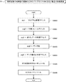
次に、更新情報ファイル50の詳細について説明する。更新情報ファイル50は、組込み機器のプログラムを更新するために使用される。上述の通り、更新情報ファイル50は、ロールバック情報の配置アドレス64、アドレス変換テーブル52、インジェクションコード70、更新差分プログラムオブジェクトコード51で構成される(図17)。以下に、更新情報ファイル50を構成する要素のそれぞれを説明する。   Next, details of the update information file 50 will be described. The update information file 50 is used for updating the program of the embedded device. As described above, the update information file 50 includes the rollback information arrangement address 64, the address conversion table 52, the injection code 70, and the update difference program object code 51 (FIG. 17). Hereinafter, each element constituting the update information file 50 will be described.

ロールバック情報の配置アドレス64は、例えばプログラム更新で何らかの異常を検知した際のプログラム復元ポイントを構成する情報である。本実施の形態では、以前にパッチ当てを実施した更新差分プログラムオブジェクトコードに対応するアドレス変換テーブルの記憶領域の先頭アドレスを示す。ここで、アドレス変換テーブルはデータROM408などに格納されているものとする。アドレス変換テーブルは、複数配置されている可能性がある。なお、どのアドレス変換テーブルも参照しない状態、即ち、どのパッチ当ても行われていない状態を復元ポイントとして指定する場合は、アドレス変換器402を無効化するためのインジェクションコードの生成が実施される。   The rollback information arrangement address 64 is information constituting a program restoration point when, for example, some abnormality is detected in the program update. In this embodiment, the start address of the storage area of the address conversion table corresponding to the update difference program object code that has been patched before is shown. Here, it is assumed that the address conversion table is stored in the data ROM 408 or the like. There may be a plurality of address conversion tables. When a state in which no address conversion table is referenced, that is, a state in which no patch is applied is designated as a restoration point, an injection code for invalidating the address converter 402 is generated.

アドレス変換テーブル52は、上述の通り、更新前プログラムのパッチ当て対象コード部の先頭アドレスを変換元アドレスとし、このパッチの先頭アドレスを変換先アドレスとした、更新差分プログラム実行のためのアドレス変換の対応関係を記載したテーブルである。なお、本実施の形態では、具体的には、アドレス変換テーブル52は、変換元アドレスの上位アドレスと変換先アドレスの上位アドレスとの対応関係を記載したテーブルである。ここで、アドレス変換の対応関係は、k個まで指定可能であるとする。kは例えば32などの定数であり、ハードウェア仕様等により定まる。   As described above, the address conversion table 52 is used for address conversion for executing an update difference program using the start address of the patch application target code portion of the pre-update program as the conversion source address and the start address of the patch as the conversion destination address. It is a table describing the correspondence. In the present embodiment, specifically, the address conversion table 52 is a table that describes the correspondence between the upper address of the source address and the upper address of the destination address. Here, it is assumed that up to k correspondence relationships for address translation can be designated. k is a constant such as 32, and is determined by the hardware specification or the like.

インジェクションコード70は、更新差分プログラムのオブジェクトコード51のプログラムROM407への配置、アドレス変換テーブル52のデータROM408への配置、アドレス変換テーブル52のアドレス変換器402への設定、アドレス変換器402の有効化、必要に応じたプログラムROM407又はデータROM408のデータ消去、異常検出などをトリガとしたロールバック処理、これら処理を実行するためのBIOSプログラムのデータROM408からプログラムROM407への展開、などを実行するためのBIOSプログラムを呼び出すために使用されるプログラム群である。ここで、インジェクションコードは、対応するBIOSルーチンへ適切な引数を渡して、BIOSルーチンを呼び出すプログラムである。インジェクションコードの実行方法としては、例えば、CANインターフェース409を介してSRAM406にインジェクションコードを配置し、割込みコントローラ403によりプログラムカウンタをインジェクションコードが配置されたアドレスへと遷移させ、インジェクションコードを実行する。インジェクションコードの実行により対応するBIOSが起動し、更新差分バイナリなどCANインターフェース409を介してSRAM406に転送されたデータのプログラムROM407/データROM408へのデータ配置が実施される。ここで、BIOSコードの配置位置は、プログラムROM407の実行中ではない面であっても良いし、データROM408の実行中ではない面であっても良い。また、インジェクションコードの実行はCANインターフェース409からの割込みで起動した割り込みハンドラ内で実施しても良い。また、例えば、インジェクションコードの実行を必ず割込みにて実施する場合、全BIOSコードは、実行終了時に、当該割込みのクリアを実施し、Halt命令を実行するよう記述されていてもよい。   The injection code 70 includes the arrangement of the object code 51 of the update difference program in the program ROM 407, the arrangement of the address conversion table 52 in the data ROM 408, the setting of the address conversion table 52 in the address converter 402, and the activation of the address converter 402. , Roll-out processing triggered by data erasure of the program ROM 407 or the data ROM 408, detection of abnormality, etc. as necessary, development of the BIOS program for executing these processing from the data ROM 408 to the program ROM 407, etc. It is a program group used for calling a BIOS program. Here, the injection code is a program that passes an appropriate argument to the corresponding BIOS routine and calls the BIOS routine. As a method for executing the injection code, for example, the injection code is arranged in the SRAM 406 via the CAN interface 409, the program counter is shifted to the address where the injection code is arranged by the interrupt controller 403, and the injection code is executed. The corresponding BIOS is activated by the execution of the injection code, and the data transfer to the program ROM 407 / data ROM 408 of the data transferred to the SRAM 406 via the CAN interface 409 such as update difference binary is executed. Here, the arrangement position of the BIOS code may be a surface where the program ROM 407 is not being executed, or may be a surface where the data ROM 408 is not being executed. Further, the injection code may be executed in an interrupt handler activated by an interrupt from the CAN interface 409. Further, for example, when the execution of the injection code is always performed by an interrupt, all BIOS codes may be described so that the interrupt is cleared and the Halt instruction is executed at the end of the execution.

図18は、インジェクションコードの構成例を示す模式図である。インジェクションコード70は、例えば、更新バイナリのプログラムROM407への書込み処理委譲のインジェクションコード701、アドレス変換テーブルのデータROM408への書込み処理委譲のインジェクションコード702、データROM408上のアドレス変換テーブルのロードのインジェクションコード703、アドレス変換有効化・無効化のインジェクションコード704、局所変数の初期値の更新のためのプログラムROM407の消去/書込み処理委譲のインジェクションコード705、大域変数の初期値の更新のためのデータROM408の消去/書込み処理委譲のインジェクションコード706、局所変数の初期値の更新のためのプログラムROM407の書込み処理委譲のインジェクションコード707、大域変数の初期値の更新のためのデータROM408の書込み処理委譲のインジェクションコード708、指定復元ポイントへのロールバック処理のインジェクションコード709、デフォルト動作へのロールバック処理のインジェクションコード710、更新キャンセル処理のインジェクションコード711、プログラムROM407のデフォルト面切り替えのインジェクションコード712、データROM408のデフォルト面切り替えのインジェクションコード713、更新差分コードのベリファイ処理(署名検証処理)委譲のインジェクションコード714、アドレス変換テーブルのベリファイ処理(署名検証処理)委譲のインジェクションコード715、データROM408上のBIOSコードのプログラムROM407への書込み処理委譲のインジェクションコード716、などから構成される。なお、各インジェクションコードの詳細については、後述する。   FIG. 18 is a schematic diagram illustrating a configuration example of an injection code. The injection code 70 includes, for example, an injection code 701 for delegating write processing to the update ROM program ROM 407, an injection code 702 for delegating write processing to the data ROM 408 of the address conversion table, and an injection code for loading the address conversion table on the data ROM 408. 703, address conversion validation / invalidation injection code 704, program ROM 407 deletion / delegation injection code 705 for updating the initial value of the local variable, and data ROM 408 for updating the initial value of the global variable Deletion / write process delegation injection code 706, program ROM 407 write process delegation injection code 707 for updating the initial values of local variables, global change Delegation of write processing of the data ROM 408 for updating the initial value of the data, injection code 709 of rollback processing to the specified restoration point, injection code 710 of rollback processing to the default operation, injection code of update cancellation processing 711, default code switching injection code 712 of the program ROM 407, default code switching injection code 713 of the data ROM 408, update difference code verification processing (signature verification processing) delegation injection code 714, address conversion table verification processing (signature verification) Processing) Transfer of delegation injection code 715 and BIOS code on data ROM 408 to program ROM 407 This is composed of a transfer injection code 716 and the like. Details of each injection code will be described later.

次に、インジェクションコードが実行されるまでの流れについて説明する。図19は、インジェクションコードが実行されるまでの流れを説明する模式図である。まず、管理サーバ30にて、インジェクションコードテンプレート群から作成対象のインジェクションコード(インジェクションコードAとする)のテンプレートを選択し、管理サーバ30のメモリ36上に展開する(図中(1)参照)。次に、管理サーバ30にて、インジェクションコードの引数定義に従い、インジェクションコードAへの実引数設定を実施する(図中(2)参照)。次に、実引数設定済みのインジェクションコードAを管理サーバ30のネットワーク接続部35などのネットワークI/Fからネットワーク15へ送信する(図中(3)参照)。次に、組込み機器40は、CANインターフェース409などのネットワークI/Fからネットワーク経由で実引数設定済みインジェクションコードAを受信する(図中(4)参照)。そして、例えばCANインターフェース409からの割込みでDMAコントローラ405またはCPU401上のデータ転送プログラムを起動し、SRAM406上の特定領域に実引数設定済みインジェクションコードAを配置する(図中(5)参照)。DMAコントローラ405を用いた場合は、配置完了を表す割込み通知後、CPU401上のデータ転送プログラムを用いた場合は、当該プログラムからの通知後、SRAM406の特定領域に配置した実引数設定済みインジェクションコードAが実行される。   Next, the flow until the injection code is executed will be described. FIG. 19 is a schematic diagram for explaining the flow until the injection code is executed. First, the management server 30 selects a template of an injection code to be created (injection code A) from the injection code template group and expands it on the memory 36 of the management server 30 (see (1) in the figure). Next, in the management server 30, the actual argument is set to the injection code A according to the argument definition of the injection code (see (2) in the figure). Next, the injection code A for which an actual argument has been set is transmitted from the network I / F such as the network connection unit 35 of the management server 30 to the network 15 (see (3) in the figure). Next, the embedded device 40 receives the injection code A with the actual argument set from the network I / F such as the CAN interface 409 via the network (see (4) in the figure). Then, for example, the data transfer program on the DMA controller 405 or the CPU 401 is activated by an interrupt from the CAN interface 409, and the injection code A with actual arguments set is arranged in a specific area on the SRAM 406 (see (5) in the figure). When the DMA controller 405 is used, after the interrupt notification indicating the completion of arrangement, when the data transfer program on the CPU 401 is used, after the notification from the program, the actual argument set injection code A arranged in the specific area of the SRAM 406 Is executed.

以下、各インジェクションコードについて説明する。図20は、データROM408上のアドレス変換テーブルのロードを行うインジェクションコード703、更新差分コードのベリファイ処理委譲を行うインジェクションコード714、又はアドレス変換テーブルのベリファイ処理委譲を行うインジェクションコード715での処理に対応するBIOSルーチンコードの呼び出し処理の手続き例を示すフローチャートである。   Hereinafter, each injection code will be described. FIG. 20 corresponds to the processing in the injection code 703 for loading the address conversion table on the data ROM 408, the injection code 714 for delegating the update difference code verification process, or the injection code 715 for delegating the address conversion table verification process. It is a flowchart which shows the example of a procedure of the calling process of the BIOS routine code to be performed.

まず、ステップ2000(S2000)で、第一引数arg1にデータ先頭アドレスを配置する。データROM408上のアドレス変換テーブルのロードを行うインジェクションコード703の場合、読み出し元の先頭アドレスが、第一引数arg1に設定される。また、更新差分コードのベリファイ処理委譲を行うインジェクションコード714及びアドレス変換テーブルのベリファイ処理委譲を行うインジェクションコード715の場合、ベリファイする対象の先頭アドレスが第一引数arg1に設定される。次に、ステップ2001(S2001)で第二引数arg2にデータ長を配置する。データROM408上のアドレス変換テーブルのロードを行うインジェクションコード703の場合、読み出されるデータのデータ長が、第二引数arg2に設定される。また、更新差分コードのベリファイ処理委譲を行うインジェクションコード714及びアドレス変換テーブルのベリファイ処理委譲を行うインジェクションコード715の場合、ベリファイする対象のデータ長が第二引数arg2に設定される。次に、ステップ2002(S2002)で、対応するBIOSルーチンのコールを実施する。   First, in step 2000 (S2000), the data head address is arranged in the first argument arg1. In the case of the injection code 703 for loading the address conversion table on the data ROM 408, the read start address is set to the first argument arg1. In addition, in the case of the injection code 714 that delegates the verification process of the update difference code and the injection code 715 that delegates the verification process of the address conversion table, the first address arg1 is set as the first address to be verified. Next, in step 2001 (S2001), the data length is arranged in the second argument arg2. In the case of the injection code 703 that loads the address conversion table on the data ROM 408, the data length of the read data is set in the second argument arg2. In addition, in the case of the injection code 714 for delegating the verification process of the update difference code and the injection code 715 for delegating the address conversion table, the data length to be verified is set in the second argument arg2. Next, in step 2002 (S2002), the corresponding BIOS routine is called.

ここで、データROM408上のアドレス変換テーブルのロードのインジェクションコード703で呼び出されるBIOSルーチンは、データROM408上のアドレス変換テーブルのロードを実施する。実行例は、例えば以下のようになる。アドレス変換テーブルがCANインターフェース409からの割込みによりDMA転送でSRAM406に配置された状態で、更にCANインターフェース409からの割込みでデータROM408上のアドレス変換テーブルのロードのインジェクションコード703がSRAM406に配置され、割込みでこのインジェクションコードが実行され、BIOSルーチンコールが成される。そして、当該BIOSルーチンでは、SRAM406に配置されたアドレス変換テーブルをアドレス変換器402に設定する。   Here, the BIOS routine called by the injection code 703 for loading the address conversion table on the data ROM 408 loads the address conversion table on the data ROM 408. An execution example is as follows, for example. In the state where the address conversion table is arranged in the SRAM 406 by DMA transfer by the interruption from the CAN interface 409, the injection code 703 for loading the address conversion table on the data ROM 408 is arranged in the SRAM 406 by the interruption from the CAN interface 409. This injection code is executed and a BIOS routine call is made. In the BIOS routine, the address conversion table arranged in the SRAM 406 is set in the address converter 402.

更新差分コードのベリファイ処理委譲のインジェクションコード714で呼び出されるBIOSルーチンは、更新差分プログラムのオブジェクトコードの署名検証処理を実施する。実行例は、例えば以下のようになる。署名付きの更新差分プログラムのオブジェクトコードがCANインターフェース409からの割込みによりDMA転送でSRAM406に配置された状態で、更にCANインターフェース409からの割込みでこのコードのベリファイ処理委譲のインジェクションコード714がSRAM406に配置され、割込みでこのインジェクションコードが実行され、BIOSルーチンコールが成される。そして、当該BIOSルーチンでは、SRAM406に配置された更新差分プログラムのオブジェクトコードの署名検証処理を実施する。   The BIOS routine called by the injection code 714 of the update difference code verification process delegation executes the signature verification process of the object code of the update difference program. An execution example is as follows, for example. The object code of the update difference program with a signature is placed in the SRAM 406 by DMA transfer due to an interrupt from the CAN interface 409, and the verification code transfer injection code 714 of this code is placed in the SRAM 406 by an interrupt from the CAN interface 409. Then, this injection code is executed by an interrupt, and a BIOS routine call is made. In the BIOS routine, signature verification processing of the object code of the update difference program arranged in the SRAM 406 is performed.

アドレス変換テーブルのベリファイ処理委譲のインジェクションコード715で呼び出されるBIOSルーチンは、アドレス変換テーブルの署名検証処理を実施する。実行例は、例えば以下のようになる。署名付きのアドレス変換テーブルがCANインターフェース409からの割込みによりDMA転送でSRAM406に配置された状態で、更にCANインターフェース409からの割込みでアドレス変換テーブルのベリファイ処理委譲のインジェクションコード715がSRAM406に配置され、割込みでこのインジェクションコードが実行され、BIOSルーチンコールが成される。当該BIOSルーチンでは、SRAM406に配置されたアドレス変換テーブルの署名検証を実施する。   The BIOS routine called by the address conversion table verification process delegation injection code 715 executes signature verification processing of the address conversion table. An execution example is as follows, for example. In a state where the signed address conversion table is arranged in the SRAM 406 by DMA transfer by interruption from the CAN interface 409, the address conversion table verification processing delegation injection code 715 is arranged in the SRAM 406 by interruption from the CAN interface 409. This injection code is executed by an interrupt, and a BIOS routine call is made. In the BIOS routine, signature verification of the address conversion table arranged in the SRAM 406 is performed.

図21は、アドレス変換テーブルのデータROM408への書込み処理委譲を行うインジェクションコード702での処理に対応するBIOSルーチンコードの呼び出し処理の手続き例を示すフローチャートである。まず、ステップ2100(S2100)で、第一引数arg1に読出しデータの先頭アドレスを配置し、ステップ2101(S2101)で、第二引数arg2にデータ長を配置し、ステップ2102(S2102)で、第三引数arg3にデータ書込み先の先頭アドレスを配置し、ステップ2103(S2103)で、対応するBIOSルーチンのコールを実施する。ここで、アドレス変換テーブルのデータROM408への書込み処理委譲のインジェクションコード702で呼び出されるBIOSルーチンは、アドレス変換テーブルのデータROM408への書込み処理を実施する。実行例は、例えば以下のようになる。アドレス変換テーブルがCANインターフェース409からの割込みにてDMA転送でSRAM406に配置された状態で、更にCANインターフェース409からの割込みでアドレス変換テーブルのデータROM408への書込み処理委譲のインジェクションコード702がSRAM406に配置され、割込みでこのインジェクションコードが実行され、BIOSルーチンコールが成される。当該BIOSルーチンでは、SRAM406に配置されたアドレス変換テーブルのデータROM408への書込み処理を実施する。   FIG. 21 is a flowchart showing a procedure example of a BIOS routine code calling process corresponding to the process in the injection code 702 for delegating the writing process of the address conversion table to the data ROM 408. First, in step 2100 (S2100), the top address of the read data is arranged in the first argument arg1, and in step 2101 (S2101), the data length is arranged in the second argument arg2, and in step 2102 (S2102), the third The head address of the data write destination is arranged in the argument arg3, and the corresponding BIOS routine is called in step 2103 (S2103). Here, the BIOS routine called by the injection code 702 for transferring the address conversion table to the data ROM 408 executes the process of writing the address conversion table to the data ROM 408. An execution example is as follows, for example. In the state where the address conversion table is arranged in the SRAM 406 by DMA transfer by the interruption from the CAN interface 409, the injection code 702 for delegating the writing process to the data ROM 408 of the address conversion table is arranged in the SRAM 406 by the interruption from the CAN interface 409. Then, this injection code is executed by an interrupt, and a BIOS routine call is made. In the BIOS routine, the address conversion table arranged in the SRAM 406 is written into the data ROM 408.

図22に更新差分プログラムのオブジェクトコードのプログラムROM407への書込み処理委譲を行うインジェクションコード701、又はデータROM408上に配置されたBIOSルーチンコードのプログラムROM407への書込み処理委譲を行うインジェクションコード716での処理に対応するBIOSルーチンコードの呼び出し処理の手続き例を示すフローチャートである。まずステップ2200(S2200)で、第一引数arg1にプログラムROM407への書込み処理プログラム(ドライバ)が配置される、SRAM406上のアドレスを配置する。なお、書込み処理プログラムはプログラムROM407の特定のアドレスに予め配置されている。次に、ステップ2201(S2201)で、第二引数arg2に、この書込み処理プログラムへ渡す引数のフレームポインタを配置する。なお、ステップ2200及びステップ2201で設定される引数は、ROMのドライバを動作させるのに必要な引数である。これは、プログラムROM407の書き換えをSRAM406上で実行する必要があることに起因している。続いて、ステップ2202(S2202)で、第三引数arg3に読出しデータの先頭アドレスを配置し、ステップ2203(S2203)で、第四引数arg4に読み出しデータのデータ長を配置し、ステップ2204(S2204)で、第五引数arg5にデータ書込み先の先頭アドレスを配置する。そして、ステップ2205(S2205)で、対応するBIOSルーチンのコールを実施する。   FIG. 22 shows the processing by the injection code 701 for delegating the writing process of the object code of the update difference program to the program ROM 407 or the injection code 716 for delegating the writing process of the BIOS routine code arranged on the data ROM 408 to the program ROM 407. 5 is a flowchart showing an example of a procedure for calling a BIOS routine code corresponding to the above. First, in step 2200 (S2200), an address on the SRAM 406 where the write processing program (driver) to the program ROM 407 is arranged in the first argument arg1. Note that the write processing program is arranged in advance at a specific address in the program ROM 407. Next, in step 2201 (S2201), the frame pointer of the argument to be passed to the write processing program is placed in the second argument arg2. The arguments set in step 2200 and step 2201 are arguments necessary for operating the ROM driver. This is because the program ROM 407 needs to be rewritten on the SRAM 406. Subsequently, in step 2202 (S2202), the top address of the read data is arranged in the third argument arg3, in step 2203 (S2203), the data length of the read data is arranged in the fourth argument arg4, and step 2204 (S2204). Thus, the top address of the data write destination is arranged in the fifth argument arg5. In step 2205 (S2205), the corresponding BIOS routine is called.

ここで、更新差分プログラムのオブジェクトコードのプログラムROM407への書込み処理委譲のインジェクションコード701で呼び出されるBIOSルーチンは、プログラムROM407への書込み処理プログラムを第一引数に指定されたSRAM406のアドレスに配置し、第二引数に指定されたフレームポインタをこの書込み処理プログラムへ引き渡し、この書込み処理プログラムを実行する事で、更新差分プログラムのオブジェクトコードのプログラムROM407への書込み処理を実施する。実行例は、例えば以下のようになる。更新差分プログラムのオブジェクトコードがCANインターフェース409からの割込みにてDMA転送でSRAM406に配置された状態で、更にCANインターフェース409からの割込みで更新差分プログラムのオブジェクトコードのプログラムROM407への書込み処理委譲のインジェクションコード701がSRAM406に配置され、割込みでこのインジェクションコードが実行され、BIOSルーチンコールが成される。当該BIOSルーチンでは、SRAM406に配置された更新差分プログラムのオブジェクトコードのプログラムROM407への書込み処理を実施する。ここで、SRAM406に配置されたプログラムROM407への書込み処理プログラムは、SRAM406をワークメモリとして用いる専用ハードウェアとして実現されていても良い。   Here, the BIOS routine called by the injection code 701 for transferring the object code of the update difference program to the program ROM 407 places the write processing program to the program ROM 407 at the address of the SRAM 406 designated as the first argument. By passing the frame pointer designated as the second argument to this write processing program and executing this write processing program, the write processing to the program ROM 407 of the object code of the update difference program is executed. An execution example is as follows, for example. When the object code of the update difference program is arranged in the SRAM 406 by DMA transfer with an interrupt from the CAN interface 409, and further, the injection of the transfer process delegation to the program ROM 407 of the object code of the update difference program with an interrupt from the CAN interface 409 The code 701 is placed in the SRAM 406, the injection code is executed by an interrupt, and a BIOS routine call is made. In the BIOS routine, the object code of the update difference program arranged in the SRAM 406 is written into the program ROM 407. Here, the write processing program to the program ROM 407 arranged in the SRAM 406 may be realized as dedicated hardware using the SRAM 406 as a work memory.

データROM408上に配置されたBIOSルーチンコードのプログラムROM407への書込み処理委譲で呼び出されるBIOSルーチンは、プログラムROM407への書込み処理プログラムを第一引数に指定されたSRAM406のアドレスに配置し、第二引数に指定されたフレームポインタをこの書込み処理プログラムへ引き渡し、この書込み処理プログラムを実行する事で、データROM408上に配置されたBIOSルーチンコードのプログラムROM407への書込み処理を実施する。実行例は、例えば以下のようになる。CANインターフェース409からの割込みでデータROM408上に配置されたBIOSルーチンコードのプログラムROM407への書込み処理委譲のインジェクションコード716がSRAM406に配置され、割込みでこのインジェクションコードが実行され、BIOSルーチンコールが成される。当該BIOSルーチンでは、データROM408上に配置されたBIOSルーチンコードのプログラムROM407への書込み処理を実施する。   The BIOS routine called by the transfer of the BIOS routine code placed on the data ROM 408 to the program ROM 407 places the write processing program to the program ROM 407 at the address of the SRAM 406 designated as the first argument, and the second argument. The frame pointer specified in the above is transferred to the write processing program, and the write processing program is executed, whereby the BIOS routine code arranged on the data ROM 408 is written into the program ROM 407. An execution example is as follows, for example. An injection code 716 for transferring the BIOS routine code placed on the data ROM 408 by the interruption from the CAN interface 409 to the program ROM 407 is arranged in the SRAM 406, and this injection code is executed by the interruption to make a BIOS routine call. The In the BIOS routine, the BIOS routine code arranged on the data ROM 408 is written into the program ROM 407.

図23は、デフォルトプログラム動作へのロールバック処理委譲を行うインジェクションコード710、又は更新キャンセル処理委譲を行うインジェクションコード711での処理に対応するBIOSルーチンコードの呼び出し処理の手続き例を示すフローチャートである。ステップ2300(S2300)で、対応するBIOSルーチンのコールを実施する。デフォルトプログラム動作へのロールバック処理委譲のインジェクションコード710で呼び出されるBIOSルーチンは、デフォルトプログラム動作へのロールバック処理を実施する。実行例は、例えば以下のようになる。CANインターフェース409からの割込みでデフォルトプログラム動作へのロールバック処理委譲のインジェクションコード710がSRAM406に配置され、割込みでこのインジェクションコードが実行され、BIOSルーチンコールが成される。当該BIOSルーチンでは、デフォルトプログラム動作へのロールバック処理を実施する。ここで、デフォルトプログラム動作へのロールバック処理では、例えば、次の再起動でのブート時にアドレス変換器402の無効化が実施されるよう設定を行う。更新キャンセル処理委譲のインジェクションコード711で呼び出されるBIOSルーチンは、更新キャンセル処理を実施する。実行例は、例えば以下のようになる。CANインターフェース409からの割込みで更新キャンセル処理委譲のインジェクションコード711がSRAM406に配置され、割込みでこのインジェクションコードが実行され、BIOSルーチンコールが成される。当該BIOSルーチンでは、更新キャンセル処理を実施する。ここで、更新キャンセル処理では、例えば、プログラムROM407又はデータROM408への書込みがどこまで成されたかの確認をし、書込まれた部分の消去を実施し、更新動作前にプログラム状態を退避していた場合は、プログラム状態の復旧を実施し、退避した状態からのプログラムの再開処理を実施する。   FIG. 23 is a flowchart showing an example of a procedure for calling a BIOS routine code corresponding to the processing in the injection code 710 for delegating rollback processing to the default program operation or the injection code 711 for delegating update cancellation processing. In step 2300 (S2300), the corresponding BIOS routine is called. The BIOS routine called by the injection code 710 for delegating the rollback process to the default program operation performs the rollback process to the default program operation. An execution example is as follows, for example. An injection code 710 for delegating rollback processing to the default program operation is placed in the SRAM 406 by interruption from the CAN interface 409, and this injection code is executed by interruption to make a BIOS routine call. In the BIOS routine, a rollback process to the default program operation is performed. Here, in the rollback process to the default program operation, for example, a setting is made so that the address converter 402 is invalidated at the time of booting at the next restart. The BIOS routine called by the update cancel process delegation injection code 711 executes the update cancel process. An execution example is as follows, for example. An update cancel process delegation injection code 711 is arranged in the SRAM 406 by an interrupt from the CAN interface 409, and this injection code is executed by an interrupt to make a BIOS routine call. In the BIOS routine, update cancellation processing is performed. Here, in the update cancellation process, for example, it is confirmed how far the program ROM 407 or the data ROM 408 has been written, the written portion is erased, and the program state is saved before the update operation Implements program state recovery and resumes the program from the saved state.

図24は、指定復元ポイントへのロールバック処理委譲を行うインジェクションコード709での処理に対応するBIOSルーチンコードの呼び出し処理の手続き例を示すフローチャートである。なお、ロールバックに際し、例えば以下のような前提がある。すなわち、既に複数回、更新差分コードがプログラムROM407に配置されている事、更新差分コードのうち、初期値付き局所変数と大域変数を除くプログラムは上書きされる事なくプログラムROM407に配置されたままである事、及びアドレス変換テーブルがデータROM408に格納されているのと同様にデータROM408にこれまでの更新差分コードに含まれた初期値付き局所変数や大域変数が格納されている事、が前提となっている。ここで、どの更新差分コード(初期値付き局所変数と大域変数を除くプログラム)にロールバックするかは、対応するアドレス変換テーブルを設定する事で可能となる。ただし、初期値付き局所変数と大域変数に関しては、何度かの更新で既に上書きされている可能性があり、ロールバックの際に書き戻す必要がある。   FIG. 24 is a flowchart showing a procedure example of a BIOS routine code calling process corresponding to the process in the injection code 709 for delegating the rollback process to the designated restoration point. Note that the following assumptions are made when rolling back. That is, the update difference code has already been arranged in the program ROM 407 a plurality of times, and among the update difference codes, the programs excluding local variables with initial values and global variables remain in the program ROM 407 without being overwritten. As well as the fact that the address conversion table is stored in the data ROM 408, the data ROM 408 stores the local variables with initial values and the global variables included in the update difference code so far. ing. Here, which update difference code (program excluding local variables with initial values and global variables) can be rolled back by setting a corresponding address conversion table. However, local variables with initial values and global variables may have been overwritten by several updates, and must be written back at the time of rollback.

ステップ2400(S2400)で、第一引数arg1に復元ポイントに対応するアドレス変換テーブルの先頭アドレスを配置する。ステップ2401(S2401)で、第二引数arg2に復元ポイントに対応するアドレス変換テーブルのエントリ数を配置する。ステップ2402(S2402)で、復元ポイントに対応するアドレス変換テーブルの設定を実施するBIOSルーチンAのコールを実施する。そして、以下のステップ2403〜2407を必要回数だけ実施する。ステップ2403(S2403)で、第一引数arg1に消去ブロック番号を配置する。この消去ブロック番号は、変数更新を実現するためのプログラムROM407又はデータROM408の消去対象のブロック番号である。ステップ2404(S2404)で、第二引数arg2にロールバック対象の差分プログラム内の変数更新部分に対応するコードが配置されているデータROM408上の領域の先頭アドレスを配置する。すなわち、この先頭アドレスは、読み出しデータの先頭アドレスである。ステップ2405(S2405)で、第三引数arg3に読み出しデータのデータ長を配置する。ステップ2406(S2406)で、第四引数arg4にデータ書込み先の先頭アドレスを配置する。ステップ2407(S2407)で、指定復元ポイントでの初期値付き局所変数や大域変数の配置状態の実現のためのプログラムROM407及びデータROM408の消去及び書込みを行うBIOSルーチンBのコールを実施する。上述のような引数の設定により、データROM408に格納された、これまでの更新差分コードに含まれた初期値付き局所変数や大域変数のうち書き込み対象となるものが、書き込まれる。具体的には、局所変数の場合にはプログラム実行のために指定されたプログラムROM407上のアドレスを先頭アドレスとする領域へと書き込まれ、大域変数の場合にはプログラム実行のために指定されたデータROM408上のアドレスを先頭アドレスとする領域へと書込まれる。ここで、指定復元ポイントへのロールバック処理委譲のインジェクションコード709で呼び出されるBIOSルーチンは、指定復元ポイントへのロールバック処理を実施する。実行例は、例えば以下のようになる。CANインターフェース409からの割込みで指定復元ポイントへのロールバック処理委譲のインジェクションコード709がSRAM406に配置され、割込みでこのインジェクションコードが実行され、BIOSルーチンコールが成される。当該BIOSルーチンでは、指定復元ポイントへのロールバック処理を実施する。ここで、指定復元ポイントへのロールバック処理では、先ず最初に指定された復元ポイントに対応するアドレス変換テーブルをアドレス変換器402に設定し、次いで、指定復元ポイントでの初期値付き局所変数や大域変数の配置状態の実現のためのプログラムROM407及びデータROM408の消去及び書込み処理を実施する。   In step 2400 (S2400), the first address of the address conversion table corresponding to the restoration point is arranged in the first argument arg1. In step 2401 (S2401), the number of entries in the address translation table corresponding to the restoration point is arranged in the second argument arg2. In step 2402 (S2402), a BIOS routine A call for setting the address translation table corresponding to the restoration point is executed. Then, the following steps 2403 to 2407 are performed as many times as necessary. In step 2403 (S2403), the erase block number is arranged in the first argument arg1. This erase block number is a block number to be erased in the program ROM 407 or the data ROM 408 for realizing variable update. In step 2404 (S2404), the start address of the area on the data ROM 408 in which the code corresponding to the variable update portion in the difference program to be rolled back is arranged in the second argument arg2. That is, this head address is the head address of read data. In step 2405 (S2405), the data length of the read data is arranged in the third argument arg3. In step 2406 (S2406), the head address of the data write destination is arranged in the fourth argument arg4. In step 2407 (S2407), the BIOS routine B is called to erase and write the program ROM 407 and the data ROM 408 for realizing the arrangement state of local variables with initial values and global variables at the designated restoration point. By setting the arguments as described above, a local variable with an initial value and a global variable stored in the data ROM 408 and included in the update difference code so far are written. Specifically, in the case of a local variable, it is written into an area starting from the address on the program ROM 407 designated for program execution. In the case of a global variable, data designated for program execution is written. Data is written into the area having the address on the ROM 408 as the head address. Here, the BIOS routine called by the injection code 709 for delegating the rollback process to the designated restoration point performs the rollback process to the designated restoration point. An execution example is as follows, for example. An injection code 709 for delegating rollback processing to a designated restoration point is arranged in the SRAM 406 by interruption from the CAN interface 409, and this injection code is executed by interruption to make a BIOS routine call. In the BIOS routine, rollback processing to the designated restoration point is performed. Here, in the rollback process to the designated restoration point, first, the address translation table corresponding to the designated restoration point is set in the address translator 402, and then local variables with initial values and global values at the designated restoration point are set. The program ROM 407 and the data ROM 408 are erased and written for realizing the variable arrangement state.

図25は、プログラムROM407のデフォルトプログラム配置面の切り替え処理委譲を行うインジェクションコード712、又はデータROM408のデフォルトプログラム配置面の切り替え処理委譲を行うインジェクションコード713での処理に対応するBIOSルーチンコードの呼び出し処理の手続き例を示すフローチャートである。ステップ2500(S2500)で、第一引数arg1にデフォルトとして使用するROMの先頭アドレスを配置し、ステップ2501(S2501)で、対応するBIOSルーチンのコールを実施する。ここで、プログラムROM407のデフォルトプログラム配置面の切り替え処理委譲のインジェクションコード712で呼び出されるBIOSルーチンは、プログラムROM407のデフォルトプログラム配置面の切り替え処理を実施する。また、データROM408のデフォルトプログラム配置面の切り替え処理委譲のインジェクションコード713で呼び出されるBIOSルーチンは、データROM408のデフォルトプログラム配置面の切り替え処理を実施する。実行例は、例えば以下のようになる。CANインターフェース409からの割込みでプログラムROM407及びデータROM408のデフォルトプログラム配置面の切り替え処理委譲のインジェクションコード712、713がSRAM406に配置され、割込みでこのインジェクションコードが実行され、BIOSルーチンコールが成される。当該BIOSルーチンでは、プログラムROM407及びデータROM408のデフォルトプログラム配置面の切り替え処理を実施する。   FIG. 25 shows the BIOS routine code call processing corresponding to the processing in the injection code 712 for delegating the switching process of the default program arrangement plane in the program ROM 407 or the injection code 713 for delegating the switching process of the default program arrangement plane in the data ROM 408. It is a flowchart which shows the example of a procedure of. In step 2500 (S2500), the start address of the ROM used as a default is placed in the first argument arg1, and in step 2501 (S2501), the corresponding BIOS routine is called. Here, the BIOS routine called by the injection code 712 for delegating the default program arrangement plane in the program ROM 407 executes the process for switching the default program arrangement plane in the program ROM 407. Also, the BIOS routine called by the injection code 713 for delegating the default program arrangement plane of the data ROM 408 performs the process of switching the default program arrangement plane of the data ROM 408. An execution example is as follows, for example. By the interruption from the CAN interface 409, the injection codes 712 and 713 for delegating the switching process of the default program arrangement plane of the program ROM 407 and the data ROM 408 are arranged in the SRAM 406, and this injection code is executed by the interruption to make a BIOS routine call. In the BIOS routine, a process for switching the default program arrangement plane of the program ROM 407 and the data ROM 408 is performed.

図26は、大域変数更新の実現のためのデータROM408の消去及び書込み処理委譲を行うインジェクションコード706での処理に対応するBIOSルーチンコードの呼び出し処理の手続き例を示すフローチャートである。ステップ2600(S2600)で、第一引数arg1に消去ブロック番号を配置する。この消去ブロック番号は、変数更新を実現するためのデータROM408の消去対象のブロック番号である。ステップ2601(S2601)で、第二引数arg2にロールバック対象の差分プログラム内の大域変数更新部分に対応するコードが配置されているデータROM408またはSRAM406上の領域の先頭アドレスを配置する。すなわち、この先頭アドレスは、読み出しデータの先頭アドレスである。ステップ2602(S2602)で、第三引数arg3に読み出しデータのデータ長を配置する。ステップ2603(S2603)で、第四引数arg4にデータ書込み先の先頭アドレスを配置する。ステップ2604(S2604)で、対応するBIOSルーチンのコールを実施する。ここで、大域変数更新の実現のためのデータROM408の消去及び書込み処理委譲のインジェクションコード706で呼び出されるBIOSルーチンは、大域変数更新の実現のためのデータROM408の消去及び書込み処理を実施する。実行例は、例えば以下のようになる。CANインターフェース409からの割込みで大域変数更新の実現のためのデータROM408の消去及び書込み処理委譲のインジェクションコード706がSRAM406に配置され、割込みでこのインジェクションコードが実行され、BIOSルーチンコールが成される。当該BIOSルーチンでは、大域変数更新の実現のためのデータROM408の消去及び書込み処理を実施する。   FIG. 26 is a flowchart showing a procedure example of a BIOS routine code calling process corresponding to the process in the injection code 706 for erasing the data ROM 408 and delegating the write process for realizing the global variable update. In step 2600 (S2600), the erase block number is arranged in the first argument arg1. This erase block number is a block number to be erased in the data ROM 408 for realizing variable update. In step 2601 (S2601), the start address of the area on the data ROM 408 or the SRAM 406 in which the code corresponding to the global variable update part in the difference program to be rolled back is arranged in the second argument arg2. That is, this head address is the head address of read data. In step 2602 (S2602), the data length of the read data is arranged in the third argument arg3. In step 2603 (S2603), the head address of the data write destination is arranged in the fourth argument arg4. In step 2604 (S2604), the corresponding BIOS routine is called. Here, the BIOS routine called by the injection code 706 for erasing and writing the data ROM 408 for realizing the global variable update performs the erasing and writing process for the data ROM 408 for realizing the global variable update. An execution example is as follows, for example. An injection code 706 for erasing and delegating the data ROM 408 for realizing the global variable update by interruption from the CAN interface 409 is arranged in the SRAM 406, and this injection code is executed by interruption to make a BIOS routine call. In the BIOS routine, the data ROM 408 is erased and written to realize global variable update.

図27は、大域変数更新の実現のためのデータROM408の書込み処理委譲を行うインジェクションコード708での処理に対応するBIOSルーチンコードの呼び出し処理の手続き例を示すフローチャートである。ステップ2700(S2700)で、第一引数arg1にロールバック対象の差分プログラム内の大域変数更新部分に対応するコードが配置されている領域(データROM408またはSRAM406)上の先頭アドレスを配置する。すなわち、この先頭アドレスは、読み出しデータの先頭アドレスである。ステップ2701(S2701)で、第二引数arg2に読み出しデータのデータ長を配置する。ステップ2702(S2702)で、第三引数arg3にデータ書込み先の先頭アドレスを配置する。ステップ2703(S2703)で、対応するBIOSルーチンのコールを実施する。ここで、大域変数更新の実現のためのデータROM408の書込み処理委譲のインジェクションコード708で呼び出されるBIOSルーチンは、大域変数更新の実現のためのデータROM408の書込み処理を実施する。実行例は、例えば以下のようになる。CANインターフェース409からの割込みで大域変数更新の実現のためのデータROM408の書込み処理委譲のインジェクションコード708がSRAM406に配置され、割込みでこのインジェクションコードが実行され、BIOSルーチンコールが成される。当該BIOSルーチンでは、大域変数更新の実現のためのデータROM408の書込み処理を実施する。   FIG. 27 is a flowchart showing a procedure example of a BIOS routine code calling process corresponding to the process in the injection code 708 for delegating the writing process of the data ROM 408 for realizing the global variable update. In step 2700 (S2700), the first address arg1 is assigned the head address on the area (data ROM 408 or SRAM 406) where the code corresponding to the global variable update part in the rollback target difference program is placed. That is, this head address is the head address of read data. In step 2701 (S2701), the data length of the read data is arranged in the second argument arg2. In step 2702 (S2702), the start address of the data write destination is arranged in the third argument arg3. In step 2703 (S2703), the corresponding BIOS routine is called. Here, the BIOS routine called by the injection code 708 for delegating the write process of the data ROM 408 for realizing the global variable update implements the write process of the data ROM 408 for realizing the global variable update. An execution example is as follows, for example. An injection code 708 for delegating the write processing of the data ROM 408 for realizing the global variable update by interruption from the CAN interface 409 is arranged in the SRAM 406, and this injection code is executed by interruption to make a BIOS routine call. In the BIOS routine, a writing process of the data ROM 408 for realizing global variable update is performed.

図28は、局所変数更新実現のためのプログラムROM407の消去及び書込み処理委譲を行うインジェクションコード705での処理に対応するBIOSルーチンコードの呼び出し処理の手続き例を示すフローチャートである。まず、ステップ2800(S2800)で、第一引数arg1に、プログラムROM407に対する消去及び書込み処理プログラム(ドライバ)が配置される、SRAM406上のアドレスを配置する。なお、消去及び書込み処理プログラムはプログラムROM407の特定のアドレスに予め配置されている。次に、ステップ2801(S2801)で、第二引数arg2に、この消去及び書込み処理プログラムへ渡す引数のフレームポインタを配置する。なお、ステップ2800及びステップ2801で設定される引数は、ROMのドライバを動作させるのに必要な引数である。これは、プログラムROM407の書き換えをSRAM406上で実行する必要があることに起因している。続いて、ステップ2802(S2802)で、第三引数arg3に消去ブロック番号を配置する。この消去ブロック番号は、変数更新を実現するためのプログラムROM407の消去対象のブロック番号である。ステップ2803(S2803)で、第四引数arg4に、ロールバック対象の差分プログラム内の局所変数更新部分に対応するコードが配置されているデータROM408またはSRAM406上の領域の先頭アドレスを配置する。すなわち、この先頭アドレスは、読み出しデータの先頭アドレスである。ステップ2804(S2804)で、第五引数arg5に読み出しデータのデータ長を配置する。ステップ2805(S2805)で、第六引数arg6にデータ書込み先の先頭アドレスを配置する。ステップ2806(S2806)で、対応するBIOSルーチンのコールを実施する。ここで、局所変数更新の実現のためのプログラムROM407の消去及び書込み処理委譲のインジェクションコード705で呼び出されるBIOSルーチンは、プログラムROM407に対する消去及び書込みプログラムを第一引数に指定されたSRAM406のアドレスに配置し、第二引数に指定されたフレームポインタをこの消去及び書込みプログラムへ引き渡し、この消去及び書込みプログラムを実行する事で、局所変数更新の実現のためのプログラムROM407の消去及び書込み処理を実施する。実行例は、例えば以下のようになる。CANインターフェース409からの割込みで局所変数更新の実現のためのプログラムROM407の消去及び書込み処理委譲のインジェクションコード705がSRAM406に配置され、割込みでこのインジェクションコードが実行され、BIOSルーチンコールが成される。当該BIOSルーチンでは、局所変数更新の実現のためのプログラムROM407の消去及び書込み処理を実施する。ここで、SRAM406に配置されたプログラムROM407に対する消去及び書込みプログラムは、SRAM406をワークメモリとして用いる専用ハードウェアとして実現されていても良い。   FIG. 28 is a flowchart showing a procedure example of a BIOS routine code calling process corresponding to the process in the injection code 705 for erasing and writing the program ROM 407 for realizing the local variable update. First, in step 2800 (S2800), an address on the SRAM 406 where the erasing and writing processing program (driver) for the program ROM 407 is arranged is arranged in the first argument arg1. Note that the erase and write processing program is arranged in advance at a specific address in the program ROM 407. Next, in step 2801 (S2801), a frame pointer of an argument to be passed to the erase and write processing program is arranged in the second argument arg2. The arguments set in step 2800 and step 2801 are arguments necessary for operating the ROM driver. This is because the program ROM 407 needs to be rewritten on the SRAM 406. Subsequently, in step 2802 (S2802), the erase block number is arranged in the third argument arg3. This erase block number is a block number to be erased in the program ROM 407 for realizing variable update. In step 2803 (S2803), the top address of the area on the data ROM 408 or the SRAM 406 in which the code corresponding to the local variable update part in the difference program to be rolled back is arranged in the fourth argument arg4. That is, this head address is the head address of read data. In step 2804 (S2804), the data length of the read data is arranged in the fifth argument arg5. In step 2805 (S2805), the start address of the data write destination is arranged in the sixth argument arg6. In step 2806 (S2806), the corresponding BIOS routine is called. Here, the BIOS routine called by the injection code 705 for erasing and writing the program ROM 407 for realizing the local variable update places the erasing and writing program for the program ROM 407 at the address of the SRAM 406 designated as the first argument. Then, the frame pointer specified as the second argument is transferred to the erase and write program, and the erase and write program is executed to execute the erase and write processing of the program ROM 407 for realizing the local variable update. An execution example is as follows, for example. An injection code 705 for erasing and delegating the program ROM 407 for realizing the local variable update by interruption from the CAN interface 409 is arranged in the SRAM 406, and this injection code is executed by interruption to make a BIOS routine call. In the BIOS routine, the program ROM 407 is erased and written to realize local variable update. Here, the erasing and writing program for the program ROM 407 arranged in the SRAM 406 may be realized as dedicated hardware using the SRAM 406 as a work memory.

図29は、局所変数更新の実現のためのプログラムROM407の書込み処理委譲を行うインジェクションコード707での処理に対応するBIOSルーチンコードの呼び出し処理の手続き例を示すフローチャートである。まず、ステップ2900(S2900)で、第一引数arg1にプログラムROM407への書込み処理プログラム(ドライバ)が配置される、SRAM406上のアドレスを配置する。なお、書込み処理プログラムはプログラムROM407の特定のアドレスに予め配置されている。次に、ステップ2901(S2901)で、第二引数arg2に、この書込み処理プログラムへ渡す引数のフレームポインタを配置する。なお、ステップ2900及びステップ2901で設定される引数は、ROMのドライバを動作させるのに必要な引数である。これは、プログラムROM407の書き換えをSRAM406上で実行する必要があることに起因している。続いて、ステップ2902(S2902)で、第三引数arg3にロールバック対象の差分プログラム内の局所変数更新部分に対応するコードが配置されているデータROM408またはSRAM406上の領域の先頭アドレスを配置する。すなわち、この先頭アドレスは、読み出しデータの先頭アドレスである。ステップ2903(S2903)で、第四引数arg4に読み出しデータのデータ長を配置する。ステップ2904(S2904)で、第五引数arg5にデータ書込み先の先頭アドレスを配置する。ステップ2905(S2905)で、対応するBIOSルーチンのコールを実施する。ここで、局所変数更新の実現のためのプログラムROM407の書込み処理委譲のインジェクションコード707で呼び出されるBIOSルーチンは、書込み処理プログラムを第一引数に指定されたSRAM406のアドレスに配置し、第二引数に指定されたフレームポインタをこの書込み処理プログラムへ引き渡し、この書込み処理プログラムを実行する事で、局所変数更新の実現のためのプログラムROM407の書込み処理を実施する。実行例は、例えば以下のようになる。CANインターフェース409からの割込みで局所変数更新の実現のためのプログラムROM407の書込み処理委譲のインジェクションコード707がSRAM406に配置され、割込みでこのインジェクションコードが実行され、BIOSルーチンコールが成される。当該BIOSルーチンでは、局所変数更新の実現のためのプログラムROM407の書込み処理を実施する。ここで、SRAM406に配置された書込み処理プログラムは、SRAM406をワークメモリとして用いる専用ハードウェアとして実現されていても良い。   FIG. 29 is a flowchart showing a procedure example of a BIOS routine code calling process corresponding to the process in the injection code 707 for delegating the writing process of the program ROM 407 for realizing the local variable update. First, in step 2900 (S2900), an address on the SRAM 406 where the write processing program (driver) to the program ROM 407 is arranged in the first argument arg1. Note that the write processing program is arranged in advance at a specific address in the program ROM 407. Next, in step 2901 (S2901), the frame pointer of the argument to be passed to the write processing program is arranged in the second argument arg2. The arguments set in step 2900 and step 2901 are arguments necessary for operating the ROM driver. This is because the program ROM 407 needs to be rewritten on the SRAM 406. Subsequently, in step 2902 (S2902), the top address of the area on the data ROM 408 or SRAM 406 in which the code corresponding to the local variable update portion in the difference program to be rolled back is arranged in the third argument arg3. That is, this head address is the head address of read data. In step 2903 (S2903), the data length of the read data is arranged in the fourth argument arg4. In step 2904 (S2904), the top address of the data write destination is arranged in the fifth argument arg5. In step 2905 (S2905), the corresponding BIOS routine is called. Here, the BIOS routine called by the write processing transfer injection code 707 of the program ROM 407 for realizing the local variable update places the write processing program at the address of the SRAM 406 designated as the first argument, and sets the second argument as the second argument. By passing the designated frame pointer to the write processing program and executing the write processing program, the write processing of the program ROM 407 for realizing the local variable update is performed. An execution example is as follows, for example. An injection code 707 for delegating the writing process of the program ROM 407 for realizing the local variable update by interruption from the CAN interface 409 is arranged in the SRAM 406, and this injection code is executed by interruption to make a BIOS routine call. In the BIOS routine, write processing of the program ROM 407 for realizing local variable update is performed. Here, the write processing program arranged in the SRAM 406 may be realized as dedicated hardware using the SRAM 406 as a work memory.

図30は、アドレス変換有効化・無効化処理委譲を行うインジェクションコード704での処理に対応するBIOSルーチンコードの呼び出し処理の手続き例を示すフローチャートである。ステップ3000(S3000)で、第一引数arg1にアドレス変換器402の有効化又は無効化を指定する値を配置し、ステップ3001(S3001)で、対応するBIOSルーチンのコールを実施する。ここで、アドレス変換器の有効化・無効化処理委譲のインジェクションコード704で呼び出されるBIOSルーチンは、アドレス変換器の有効化又は無効化処理を実施する。実行例は、例えば以下のようになる。CANインターフェース409からの割込みでアドレス変換有効化・無効化処理委譲のインジェクションコード704がSRAM406に配置され、割込みでこのインジェクションコードが実行され、BIOSルーチンコールが成される。当該BIOSルーチンでは、アドレス変換器の有効化又は無効化処理を実施する。   FIG. 30 is a flowchart illustrating a procedure example of a BIOS routine code calling process corresponding to the process in the injection code 704 that performs the address translation validation / invalidation process delegation. In step 3000 (S3000), a value that designates enabling or disabling of the address converter 402 is placed in the first argument arg1, and in step 3001 (S3001), a corresponding BIOS routine is called. Here, the BIOS routine called by the address translator validation / invalidation process delegation injection code 704 executes the address translator validation / invalidation process. An execution example is as follows, for example. The address translation validation / invalidation process delegation injection code 704 is arranged in the SRAM 406 by an interrupt from the CAN interface 409, and this injection code is executed by an interrupt to make a BIOS routine call. In the BIOS routine, the address converter is validated or invalidated.

以上、各種インジェクションコードについて説明した。インジェクションコードの配置及び実行、並びにインジェクションコードからコールされるBIOSルーチンの実行は、図5の構成の場合、CPU401によって行われる。一方、図6の構成の場合、メインCPU401又はサブCPU411の何れで実行しても良い。サブCPU411で実行する場合、BIOSコードをプログラムROM412に配置しても良い。プログラムROM412にBIOSコードを配置し、サブCPU411でBIOSルーチンを実行する場合であって、プログラムROM407やデータROM408への転送路が図6での破線で示すように二重化されている場合、メインCPU401で現在実行中のプログラムへの機能及び実行動作サイクルに一切影響を与える事なく、現在実行中プログラムの動作中に、更新情報ファイル50をプログラムROM407やデータROM408に動的に配置可能となる。また、破線で示すような伝送路の二重化がされていない場合は、各種BIOSコード実行によるプログラムROM407やデータROM408へのサブCPU411からのアクセスを、プリエンプティブな最低優先度アクセスとする事で、メインCPU401での現在実行中のプログラムの実行動作への影響が大幅に低減可能となる。   The various injection codes have been described above. The arrangement and execution of the injection code and the execution of the BIOS routine called from the injection code are performed by the CPU 401 in the case of the configuration of FIG. On the other hand, in the case of the configuration of FIG. When executed by the sub CPU 411, the BIOS code may be arranged in the program ROM 412. When the BIOS code is arranged in the program ROM 412 and the BIOS routine is executed by the sub CPU 411, and the transfer path to the program ROM 407 and the data ROM 408 is duplexed as shown by the broken line in FIG. The update information file 50 can be dynamically arranged in the program ROM 407 and the data ROM 408 during the operation of the currently executing program without affecting the function and execution operation cycle of the currently executing program. If the transmission path is not duplexed as indicated by the broken line, the main CPU 401 can set the access from the sub CPU 411 to the program ROM 407 and the data ROM 408 by executing various BIOS codes as a preemptive lowest priority access. The influence on the execution operation of the currently running program can be greatly reduced.

次に、インジェクションコードの構成例について説明する。図31A、31Bは、インジェクションコードの構成例を示し、図31Aは、BIOSルーチンを関数呼び出しで実行する場合に対応する例を示し、図31Bは、BIOSルーチンへのJump命令によりBIOSルーチンを実行する場合に対応する例を示す。なお、図31A及び図31Bは、いずれも、更新バイナリのプログラムROM407への書込み処理委譲のインジェクションコード701が、一例として示されている。BIOSルーチンを関数呼び出しで実行する場合、BIOS引数へのフレームポインタの設定とBIOSルーチンを関数呼び出し命令とでなるBIOSルーチン関数呼び出し部分816と、BIOSルーチンへの引数の配置部分817とからなる(図31A参照)。これに対し、BIOSルーチンへのJump命令によりBIOSルーチンを実行する場合、BIOS引数へのフレームポインタの設定とJump命令とからなるBIOSルーチン関数呼び出し部分818と、BIOSルーチンへの引数の配置部分819とからなる(図31B参照)。   Next, a configuration example of the injection code will be described. 31A and 31B show examples of the configuration of the injection code, FIG. 31A shows an example corresponding to the case where the BIOS routine is executed by function call, and FIG. 31B executes the BIOS routine by a Jump instruction to the BIOS routine. An example corresponding to the case is shown. FIG. 31A and FIG. 31B both show, as an example, an injection code 701 for delegating the write process to the update binary program ROM 407. When the BIOS routine is executed by a function call, it is composed of a BIOS routine function call part 816 in which a frame pointer is set in the BIOS argument and the BIOS routine is a function call instruction, and an argument placement part 817 in the BIOS routine (see FIG. 31A). On the other hand, when the BIOS routine is executed by the Jump instruction to the BIOS routine, the BIOS routine function calling part 818 including the setting of the frame pointer to the BIOS argument and the Jump instruction, the argument placing part 819 to the BIOS routine, (See FIG. 31B).

次に、BIOSコードの配置例について説明する。図32A、32Bは、BIOSコードの3面のプログラムROM407への配置例を示す模式図であり、図32AはBIOSコードの更新を伴わないプログラムの更新の場合に対応した例を示し、図32BはBIOSコードの更新を含むデフォルトプログラム全体の更新の場合に対応した例を示している。   Next, a BIOS code arrangement example will be described. 32A and 32B are schematic diagrams showing an example of the arrangement of the BIOS code on the three-side program ROM 407. FIG. 32A shows an example corresponding to the case of program update without BIOS code update, and FIG. An example corresponding to the update of the entire default program including the update of the BIOS code is shown.

まず、図32Aを参照してBIOSコードの更新を伴わないプログラムの更新の場合について説明する。図32Aでは、3面ともに同じBIOSコードが配置されており、A面にはデフォルトプログラムが配置され、B面には現在実行中の差分コードが配置されている。そして、A面及びB面において、デフォルトプログラムから更新されたプログラムが実行されている。ここで、C面に新たな更新差分プログラムが配置されることを考える。C面への更新差分プログラムの配置では、C面に配置されたBIOSコードが用いられる。C面への更新差分プログラムの配置では、SRAM406に展開されたプログラムROM書込みドライバが書込み実行する事で、A面及びB面へのCPU401からのアクセスを阻害する事なく、C面への更新差分プログラムの配置が可能となる。すなわち、A面及びB面でのプログラム実行中の、C面への更新差分プログラムの配置が可能となる。尚、B面もC面も、配置される更新差分プログラムは、A面に配置されたデフォルトプログラムに対する更新差分プログラムとなる。ここで、B面に配置する更新差分プログラムは、既にB面に配置されている更新差分プログラムを再利用して構成しても良い。また、C面に配置する更新差分プログラムは、既にC面に配置されている更新差分プログラムを再利用して構成しても良い。   First, with reference to FIG. 32A, a case of updating a program without updating the BIOS code will be described. In FIG. 32A, the same BIOS code is arranged on all three surfaces, the default program is arranged on the A surface, and the currently executed difference code is arranged on the B surface. And the program updated from the default program is run in A side and B side. Here, it is considered that a new update difference program is arranged on the C plane. In the arrangement of the update difference program on the C plane, the BIOS code arranged on the C plane is used. In the arrangement of the update difference program on the C plane, the program ROM write driver developed in the SRAM 406 executes the write, so that the update difference to the C plane is not hindered by the CPU 401 from accessing the A plane and the B plane. Program placement is possible. That is, the update difference program can be arranged on the C plane while executing the program on the A plane and the B plane. In addition, the update difference program arranged on both the B surface and the C surface is an update difference program for the default program arranged on the A surface. Here, the update difference program arranged on the B surface may be configured by reusing the update difference program already arranged on the B surface. Moreover, the update difference program arranged on the C plane may be configured by reusing the update difference program already arranged on the C plane.

次に、図32Bを参照して、BIOSコードの更新を含むデフォルトプログラム全体の更新の場合について説明する。図32Bは、A面及びC面を消去し、B面に新デフォルトプログラムと新BIOSコードを配置後、B面に配置された新BIOSコードをA面とC面にコピーして配置した状態を示している。これについて、次のような処理が行われる。まず、B面の消去を、プログラムROM407の消去処理委譲のインジェクションコードからプログラムROM407の消去処理BIOSを呼び出して実行する事で実施する。次に、B面への新デフォルトプログラム及び新BIOSコードの配置を、プログラムROM書込み処理委譲のインジェクションコードからプログラムROM書込み処理を呼び出して実行する事で実施する。そして、デフォルト面切り替え処理委譲のインジェクションコード712、713からデフォルト面切り替え処理BIOSを呼び出して実行する事で、再起動時の開始アドレスをB面の先頭とする。プログラムROM407のA面及びC面の再起動中の消去を実行するためのプログラムROM消去委譲のインジェクションコードと、A面及びC面への新BIOSコードの再起動中のコピーを実行するためのプログラムROM書込み処理委譲のインジェクションコードを、再起動前にSRAM406からデータROM408に配置し、再起動中にデータROM408から上記2つのインジェクションコードをSRAM406へ展開し、実行する。なお、インジェクションコードを一旦、データROM408に配置するのは、再起動の際にSRAM406の記憶内容が失われてしまうためである。再起動後には、図32Bに示すプログラム配置構造が実現され、プログラム開始アドレスがB面の先頭に設定され、B面の新デフォルトプログラムの実行がなされる。なお、新BIOSは、データROM408に一旦配置した後、適当なタイミングでプログラムROM407に展開されてもよい。   Next, with reference to FIG. 32B, a case of updating the entire default program including updating of the BIOS code will be described. FIG. 32B shows a state in which the A side and the C side are deleted, the new default program and the new BIOS code are arranged on the B side, and then the new BIOS code arranged on the B side is copied and arranged on the A side and the C side. Show. For this, the following processing is performed. First, the B side is erased by calling and executing the erase process BIOS in the program ROM 407 from the erase process transfer injection code in the program ROM 407. Next, the new default program and the new BIOS code are arranged on the B side by calling and executing the program ROM write process from the injection code of the program ROM write process delegation. Then, by calling and executing the default plane switching process BIOS from the injection codes 712 and 713 of the default plane switching process delegation, the start address at the time of restart is set to the top of the B plane. Program ROM erasure delegation injection code for executing erasure during restart of the A side and C side of the program ROM 407, and a program for executing copying during restart of the new BIOS code to the A side and C side The ROM write process delegation injection code is arranged from the SRAM 406 to the data ROM 408 before the restart, and the two injection codes are expanded from the data ROM 408 to the SRAM 406 during the restart and executed. The reason why the injection code is temporarily placed in the data ROM 408 is that the stored contents of the SRAM 406 are lost at the time of restart. After the restart, the program arrangement structure shown in FIG. 32B is realized, the program start address is set at the top of the B side, and the new default program on the B side is executed. The new BIOS may be temporarily stored in the data ROM 408 and then expanded in the program ROM 407 at an appropriate timing.

次に更新情報ファイル50の作成手順について説明する。図33A、33Bは、差分更新に対応する、更新バイナリコードと更新情報の生成の処理の一例を示すフローチャートである。本フローは、開発環境20のデータ処理部22にて実行される。下記のフローは、具体的には、例えば、データ処理部22のメモリに格納されたプログラムをデータ処理部22の処理装置が実行することにより実現される。   Next, a procedure for creating the update information file 50 will be described. 33A and 33B are flowcharts illustrating an example of a process of generating an update binary code and update information corresponding to the difference update. This flow is executed by the data processing unit 22 of the development environment 20. Specifically, the following flow is realized, for example, when the processing device of the data processing unit 22 executes a program stored in the memory of the data processing unit 22.

ステップ3300(S3300)で、データ処理部22は、変数flagに初期値0を代入する。
ステップ3301(S3301)で、データ処理部22は、ロールバックポイントの指定があるか否か判定する。指定がある場合は、処理がステップ3302へ移行する。指定がない場合、処理は、ステップ3304へ処理を移行する。
ステップ3302(S3302)で、データ処理部22は、ユーザからのロールバックポイントの指定の入力を受付けて受付けた内容を格納する。
ステップ3303(S3303)で、データ処理部22は、変数flagの値を1に更新する。
In step 3300 (S3300), the data processing unit 22 assigns an initial value 0 to the variable flag.
In step 3301 (S3301), the data processing unit 22 determines whether a rollback point is specified. If so, the process proceeds to step 3302. If there is no designation, the processing shifts to step 3304.
In step 3302 (S3302), the data processing unit 22 receives the input of the rollback point designation from the user and stores the received content.
In step 3303 (S3303), the data processing unit 22 updates the value of the variable flag to 1.

ステップ3304(S3304)で、データ処理部22は、更新前後のプログラム(アドレス未解決)を比較して差分プログラムを抽出する。本抽出では、関数構造を考慮しても良い。特に、何れか一方にのみ含まれる関数をインライン(Inline)展開せずに、コールグラフ(Call Graph)における関数名の対応を関数の対応構造として、各対応する関数毎に差分を抽出しても良い。
ステップ3305(S3305)で、データ処理部22は、差分コードを構成するコードブロック(置換ブロック)がN個以下になるよう、コードブロックを、2つのプログラム間で変化がない部分を含み得る方法でマージする。なお、Nは、例えば、アドレス変換テーブルの設定可能なエントリ数の最大値と、更新差分プログラムが配置されるメモリ領域におけるセグメント数の小さい方の値である。マージ処理の具体的な例については、図35A、35Bを参照して説明する。
In step 3304 (S3304), the data processing unit 22 compares the programs before and after the update (address unresolved) and extracts a difference program. In this extraction, a function structure may be considered. In particular, even if a function included in only one of the functions is not expanded inline, the correspondence of the function name in the call graph (Call Graph) is used as a function corresponding structure, and a difference is extracted for each corresponding function. good.
In step 3305 (S3305), the data processing unit 22 can include a portion that does not change between two programs so that the code block (replacement block) constituting the difference code is N or less. Merge. N is, for example, the maximum value of the number of entries that can be set in the address conversion table and the smaller value of the number of segments in the memory area in which the update difference program is arranged. A specific example of the merge process will be described with reference to FIGS. 35A and 35B.

ステップ3306(S3306)で、データ処理部22は、差分コードを構成するコードブロック数(置換ブロック数)を変数Mに代入する。
ステップ3307(S3307)で、データ処理部22は、変数iを1からMに1ずつ増加させながら、ステップ3308をM回繰り返す。
ステップ3308(S3308)で、データ処理部22は、リンクによるアドレス解決済みのプログラムである更新前プログラム(デフォルトプログラム)における、差分コードの第i番目のコードブロックの先頭アドレスを抽出する。この先頭アドレスは、更新の際の変換元のアドレスに相当する。データ処理部22は、このコードブロックがデフォルトプログラム内の関数を参照する場合、当該関数の呼び出しアドレスを抽出する。
In step 3306 (S3306), the data processing unit 22 assigns the number of code blocks (number of replacement blocks) constituting the difference code to the variable M.
In step 3307 (S3307), the data processing unit 22 repeats step 3308 M times while increasing the variable i from 1 to 1 by one.
In step 3308 (S3308), the data processing unit 22 extracts the head address of the i-th code block of the difference code in the pre-update program (default program) which is a program whose address has been resolved by linking. This head address corresponds to the address of the conversion source at the time of update. When the code block refers to a function in the default program, the data processing unit 22 extracts a call address of the function.

ステップ3309(S3309)で、データ処理部22は、アドレス変換テーブルに設定するセグメントサイズを決定する。なお、セグメントサイズは、変換対象となる上位アドレスのビット数に相当する。セグメントサイズの決定では、差分コードを構成する各コードブロックのサイズを考慮しても良い。例えば、サイズの最大値、中央値、又は平均を用いても良い。なお、セグメントサイズを決定する上位アドレスのビット数が少ないと、大きな差分コードの配置が特段の工夫なく配置可能となる一方、配置可能な差分コードブロックの数は少なくなる。これに対し、セグメントサイズを決定する上位アドレスのビット数が大きいと、図11A、図11B、又は図14に示したような工夫が配置の際に必要となるが、アドレス変換テーブルのエントリ数を上限として、より多くの差分コードブロックを配置することが可能となる。
ステップ3310(S3310)で、データ処理部22は、開発環境で保持している、更新対象の組込み機器40のROMの使用状況を参照し、差分プログラムを構成する各コードブロックの配置位置(先頭アドレス)を決定する。配置位置(先頭アドレス)の決定では、ステップ3309で求めたセグメントサイズ毎に高々1つのコードブロックが配置されるように決定を行うものとする。ここで、差分コードを構成するコードブロックの配置において、プログラムROM407の領域を再利用しても良い。プログラムROM407の再利用対象領域の消去回数が、どの領域でも均一となるように工夫しても良い。また、消去回数が規定回数を超える場合に、警告を発しても良い。本警告に基づき、ユーザは、差分コードによる更新ではなく、図34に示す全体プログラム更新へと、更新内容を変更しても良いし、次回の更新を全体プログラム更新としても良い。このように消去回数を参照するのは、以下の点で利点がある。すなわち、例えばROMとしてフラッシュメモリが用いられる場合、フラッシュメモリは消去書込みで劣化するため、特定領域に集中的に消去や書込みが発生しないよう工夫する事で、フラッシュメモリの寿命を延命することが可能となる。また、品質保証の観点から、書き換え回数の所定の上限を越えての書換えが起らないよう管理することが好ましい。
In step 3309 (S3309), the data processing unit 22 determines a segment size to be set in the address conversion table. The segment size corresponds to the number of bits of the upper address to be converted. In determining the segment size, the size of each code block constituting the difference code may be taken into consideration. For example, the maximum value, the median value, or the average of the sizes may be used. Note that if the number of bits of the upper address that determines the segment size is small, it is possible to arrange a large difference code without any special contrivance, while the number of difference code blocks that can be arranged decreases. On the other hand, if the number of bits of the upper address that determines the segment size is large, a device as shown in FIG. 11A, FIG. 11B, or FIG. As an upper limit, it becomes possible to arrange more differential code blocks.
In step 3310 (S3310), the data processing unit 22 refers to the use status of the ROM of the embedded device 40 to be updated, which is held in the development environment, and the arrangement position (start address) of each code block constituting the difference program ). In the determination of the arrangement position (start address), the determination is made so that at most one code block is arranged for each segment size obtained in step 3309. Here, the area of the program ROM 407 may be reused in the arrangement of code blocks constituting the difference code. You may devise so that the frequency | count of erasure | elimination of the reuse object area | region of program ROM407 may become uniform in every area | region. Further, a warning may be issued when the number of erasures exceeds a specified number. Based on this warning, the user may change the update content to the entire program update shown in FIG. 34 instead of the update by the difference code, or the next update may be the entire program update. Reference to the erase count in this way is advantageous in the following points. In other words, for example, when flash memory is used as a ROM, the flash memory deteriorates by erasing and writing. Therefore, it is possible to extend the life of the flash memory by devising that erasing and writing do not occur intensively in a specific area. It becomes. Further, from the viewpoint of quality assurance, it is preferable to manage so that rewriting exceeding a predetermined upper limit of the number of rewrites does not occur.

ステップ3311(S3311)で、データ処理部22は、更新前プログラム(リンク済)のシンボル情報を参照し、差分プログラムを構成する各コードブロックから参照される、アドレス解決済みシンボルのアドレス値を求める。そして、データ処理部22は、アドレス未解決シンボルやアドレス未解決コードのアドレス解決を、ステップ3310で決定した各コードブロックの先頭アドレスを用いて実施する。
ステップ3312(S3312)で、データ処理部22は、アドレス解決済みの差分プログラムを生成する。
ステップ3313(S3313)で、データ処理部22は、変数jを1からMへ1ずつ増加させながら、ステップ3314を繰り返す。
ステップ3314(S3314)で、データ処理部22は、差分プログラムを構成する各コードブロックjについて、ステップ3310で求めた先頭アドレスを変換後のアドレスとして抽出する。
ステップ3315(S3315)で、データ処理部22は、各コードブロックに対して、ステップ3308で求めた変換前アドレスとステップ3314で抽出した変換後のアドレスを対応表としてマージし、アドレス変換表を生成する。
ステップ3316(S3316)で、データ処理部22は、アドレス変換テーブルのデータROM408への書込み処理委譲のインジェクションコード702を生成する。
ステップ3317(S3317)で、データ処理部22は、更新バイナリのプログラムROMへの書込み処理委譲のインジェクションコード701を生成する。
ステップ3318(S3318)で、データ処理部22は、変数flagの値が1に一致するか否か判定する。一致する場合、処理はステップ3319へ移行し、一致しない場合、処理は終了する。
ステップ3319(S3319)で、データ処理部22は、指定復元ポイントへのロールバック処理委譲のインジェクションコード709を生成する。ここで、本インジェクションコードは、例えば差分プログラム更新にて途中停止やセキュリティ上の異常が発生した場合に実行される。また、本インジェクションコードから実行したロールバックBIOSコードの実行完了時に、更新キャンセルBIOSコード呼び出しが実行されるとしても良い。
In step 3311 (S3311), the data processing unit 22 refers to the symbol information of the pre-update program (linked), and obtains the address value of the address-resolved symbol that is referred to from each code block constituting the difference program. Then, the data processing unit 22 performs address resolution of the address unresolved symbol or address unresolved code using the head address of each code block determined in Step 3310.
In step 3312 (S3312), the data processing unit 22 generates an address-resolved difference program.
In step 3313 (S3313), the data processing unit 22 repeats step 3314 while increasing the variable j by 1 from 1 to M.
In step 3314 (S3314), the data processing unit 22 extracts the head address obtained in step 3310 as the converted address for each code block j constituting the difference program.
In step 3315 (S3315), the data processing unit 22 merges, for each code block, the pre-conversion address obtained in step 3308 and the post-conversion address extracted in step 3314 as a correspondence table to generate an address conversion table. To do.
In step 3316 (S3316), the data processing unit 22 generates an injection code 702 for delegating the writing process to the data ROM 408 of the address conversion table.
In step 3317 (S3317), the data processing unit 22 generates an injection code 701 for delegating the writing process of the updated binary to the program ROM.
In step 3318 (S3318), the data processing unit 22 determines whether or not the value of the variable flag matches 1. If they match, the process proceeds to step 3319. If they do not match, the process ends.
In step 3319 (S3319), the data processing unit 22 generates a rollback process delegation injection code 709 to the designated restoration point. Here, this injection code is executed when, for example, a halfway stop or a security abnormality occurs in the difference program update. Further, when the execution of the rollback BIOS code executed from this injection code is completed, the update cancel BIOS code call may be executed.

図34は、全体プログラム更新に対応する、更新バイナリコードと更新情報の生成の処理の一例を示すフローチャートである。本フローは、開発環境20のデータ処理部22にて実行される。下記のフローは、具体的には、例えば、データ処理部22のメモリに格納されたプログラムをデータ処理部22の処理装置が実行することにより実現される。   FIG. 34 is a flowchart illustrating an example of a process of generating an update binary code and update information corresponding to the entire program update. This flow is executed by the data processing unit 22 of the development environment 20. Specifically, the following flow is realized, for example, when the processing device of the data processing unit 22 executes a program stored in the memory of the data processing unit 22.

ステップ3400(S3400)で、データ処理部22は、変数flagに初期値0を代入する。
ステップ3401(S3401)で、データ処理部22は、ロールバックの指定があるか否か判定する。指定がある場合、処理はステップ3402へ移行し、指定がない場合、処理はステップ3404へ移行する。
ステップ3402(S3402)で、データ処理部22は、ユーザからのロールバックポイントの指定の入力を受付けて受付けた内容を格納する。
ステップ3403(S3403)で、データ処理部22は、変数flagの値を1に更新する。
In step 3400 (S3400), the data processing unit 22 assigns an initial value 0 to the variable flag.
In step 3401 (S3401), the data processing unit 22 determines whether rollback is designated. If so, the process proceeds to step 3402; otherwise, the process proceeds to step 3404.
In step 3402 (S3402), the data processing unit 22 receives the input of specifying the rollback point from the user and stores the received content.
In step 3403 (S3403), the data processing unit 22 updates the value of the variable flag to 1.

ステップ3404(S3404)で、データ処理部22は、更新後のプログラムのアドレス解決(リンク)を実施し、更新バイナリを生成する。
ステップ3405(S3405)で、データ処理部22は、BIOSコードのデータROM408からプログラムROM407への書込みがあるか否か判定する。書込みがある場合、処理はステップ3406へ移行し、無い場合、処理はステップ3407へ移行する。
ステップ3406(S3406)で、データ処理部22は、データROM408に格納されているBIOSコードのプログラムROM407への書込み処理委譲のインジェクションコード716を生成する。ここで、BIOSコードのプログラムROM407への書込みは、一部または全てのプログラムROM407に未だBIOSコードが配置されていない場合に実施される。3面のプログラムROM407の場合、差分コードの書込み先のプログラムROM407の面にBIOSコードが配置されていない場合、このプログラムROM面へBIOSコードを書込むこととなる。これにより、例えば予めデータROM408に格納されていたBIOSコードが、プログラムROM407に書き込まれることとなる。
ステップ3407(S3407)で、データ処理部22は、更新バイナリのプログラムROM書込み処理委譲のインジェクションコード701を生成する。ここでは、全体プログラム更新のため、本インジェクションコードは、復元ポイント無効化のためのデータROM408の消去を実行するBIOSコードの呼び出しも実施するものとする。
ステップ3408(S3408)で、データ処理部22は、プログラムROM407のデフォルト面切り替えのためのインジェクションコード712、及びデータROM408のデフォルト面切り替えのためのインジェクションコード713を生成する。
ステップ3409(S3409)で、データ処理部22は、アドレス変換テーブルの無効化を行うインジェクションコードを生成する。
In step 3404 (S3404), the data processing unit 22 performs address resolution (link) of the updated program, and generates an updated binary.
In step 3405 (S3405), the data processing unit 22 determines whether there is a writing of the BIOS code from the data ROM 408 to the program ROM 407. If there is a write, the process proceeds to step 3406; otherwise, the process proceeds to step 3407.
In step 3406 (S3406), the data processing unit 22 generates an injection code 716 for delegating the writing process to the program ROM 407 of the BIOS code stored in the data ROM 408. Here, the writing of the BIOS code to the program ROM 407 is performed when the BIOS code is not yet arranged in a part or all of the program ROM 407. In the case of the three-side program ROM 407, if the BIOS code is not arranged on the surface of the program ROM 407 to which the difference code is written, the BIOS code is written to the program ROM surface. As a result, for example, the BIOS code stored in advance in the data ROM 408 is written in the program ROM 407.
In step 3407 (S3407), the data processing unit 22 generates an update binary program ROM write process delegation injection code 701. Here, in order to update the entire program, this injection code also calls the BIOS code for executing the erasure of the data ROM 408 for invalidating the restoration point.
In step 3408 (S3408), the data processing unit 22 generates an injection code 712 for switching the default plane of the program ROM 407 and an injection code 713 for switching the default plane of the data ROM 408.
In step 3409 (S3409), the data processing unit 22 generates an injection code for invalidating the address conversion table.

ステップ3410(S3410)で、データ処理部22は、変数flagの値が1か否か比較する。一致する場合、処理はステップ3411へ移行し、不一致の場合、処理は終了する。
ステップ3411(S3411)で、データ処理部22は、デフォルト動作へのロールバック処理委譲のインジェクションコード710を生成する。ここで、本インジェクションコードは、差分プログラム更新にて途中停止やセキュリティ上の異常が発生した場合に実行される。また、本インジェクションコードから実行したロールバックBIOSコード実行完了時に、更新キャンセルBIOSコード呼び出しが実行されるとしても良い。
In step 3410 (S3410), the data processing unit 22 compares whether or not the value of the variable flag is 1. If they match, the process proceeds to step 3411. If they do not match, the process ends.
In step 3411 (S3411), the data processing unit 22 generates an injection code 710 for delegating the rollback process to the default operation. Here, this injection code is executed when an interruption or a security abnormality occurs in the difference program update. In addition, the update cancel BIOS code call may be executed when the rollback BIOS code executed from the injection code is completed.

次に、図33Aの処理ステップ3305の詳細について説明する。図35A、35Bは、図33Aのステップ3305における差分プログラムのマージの処理の一例を示すフローチャートである。なお、以下の説明において、Nは、プログラムROM407用のアドレス変換テーブルのエントリ数、すなわちアドレス変換テーブルに設定可能なアドレス変換の個数の最大値である。また、Mは、データROM408用のアドレス変換テーブルのエントリ数、すなわちアドレス変換テーブルに設定可能なアドレス変換の個数の最大値である。以下に示されるように、プログラムROM407若しくはデータROM408に配置されたデータテーブルの更新、又は新規データテーブルの追加により必要となる各種インジェクションコードの生成の実施後、差分コードを構成するコードブロックが規定個数以下のコードブロック数となるようマージ処理を実施する。なお、データテーブルとは、初期値付き局所変数又は大域変数を示すものである。ここで、同一セグメント領域内に、更新される複数のデータテーブルが配置されている場合、それらを纏めて、1つのデータテーブルとして扱うものとする。特に、図11A、11Bに示したアドレス変換処理を援用する場合、同一セグメント領域内に先頭アドレスが配置されている複数の被更新データテーブルを1つのデータテーブルとして扱っても良い。以下、図35A、35Bの説明において、データテーブルは、上述のようにセグメント毎に一つにまとめられたデータテーブルを示すものとする。また、新規データテーブルに関しては、セグメント数が最小となる配置が既に実施されているものとする。具体的には、ナップサック問題を解く事でこれが実現される。なお、セグメント数が最小となる配置の一例としては、例えば複数の新規初期値付き局所変数(配列)が同一関数内に記載されている場合に、これらを可能な限り同一セグメント内に配置することが挙げられる。また、セグメント内の一纏めとなったデータテーブルの構成要素(すなわち、結合前のデータテーブル)の夫々の先頭アドレスは、既に算出されているものとする。これら先頭アドレスは、図33Aのステップ3312でのリンク済み差分プログラムの生成の際に参照される。   Next, details of processing step 3305 in FIG. 33A will be described. FIGS. 35A and 35B are flowcharts showing an example of the difference program merging process in step 3305 of FIG. 33A. In the following description, N is the number of entries in the address conversion table for the program ROM 407, that is, the maximum number of address conversions that can be set in the address conversion table. M is the number of entries in the address translation table for the data ROM 408, that is, the maximum number of address translations that can be set in the address translation table. As shown below, the number of code blocks that make up the difference code after the generation of various injection codes required by updating the data table arranged in the program ROM 407 or the data ROM 408 or adding a new data table is specified. Merge processing is performed so that the number of code blocks is as follows. The data table indicates local variables with initial values or global variables. Here, when a plurality of data tables to be updated are arranged in the same segment area, they are collectively handled as one data table. In particular, when the address conversion process shown in FIGS. 11A and 11B is used, a plurality of update data tables in which the head address is arranged in the same segment area may be handled as one data table. Hereinafter, in the description of FIGS. 35A and 35B, the data table is a data table grouped into one segment as described above. Further, regarding the new data table, it is assumed that an arrangement that minimizes the number of segments has already been performed. Specifically, this is achieved by solving the knapsack problem. In addition, as an example of the arrangement that minimizes the number of segments, for example, when multiple local variables (arrays) with new initial values are described in the same function, these should be arranged in the same segment as much as possible. Is mentioned. In addition, it is assumed that the start addresses of the constituent elements of the data table that are grouped together in the segment (that is, the data table before joining) have already been calculated. These head addresses are referred to when the linked difference program is generated in step 3312 in FIG. 33A.

ステップ3500(S3500)で、データ処理部22は、プログラムROM407への書込みデータテーブル数をn、データROMへの書込みデータテーブル数をmとする。なお、書込みデータテーブル数とは、データテーブルの書き換え又は追加により、書き込まれるデータテーブルの数である。
ステップ3501(S3501)で、データ処理部22は、N>nかつM≧mを満たすか否か判定する。成立していれば、処理はステップ3503へ移行し、不成立であれば処理はステップ3502へ移行する。
ステップ3502(S3502)で、アドレス変換テーブルのエントリ数を超えているため、データ処理部22は、ステップ3501における違反があった書込みに関し、書き込まれるデータテーブルが含まれる隣接するセグメントのマージ処理を実施する。データ処理部22は、隣接したものがなければ、書き込まれるデータテーブルが含まれる一番近いセグメントのマージを実施する。ここで、データ処理部22は、ユーザには差分更新が不可能である旨を通知し、セグメントサイズを超えたデータテーブルの更新を許可するか否か問合せる。許可された場合、処理はステップ3500へ移行し、許可されない場合、処理は中断する。中断した場合は、ユーザが更新プログラムを修正し、再度、更新準備処理を実施するか、プログラム全体更新に方針転換を行う事となる。
In step 3500 (S3500), the data processing unit 22 sets the number of write data tables to the program ROM 407 to n and the number of write data tables to the data ROM to m. The number of write data tables is the number of data tables written by rewriting or adding data tables.
In step 3501 (S3501), the data processing unit 22 determines whether N> n and M ≧ m are satisfied. If established, the process proceeds to step 3503, and if not established, the process proceeds to step 3502.
In step 3502 (S3502), since the number of entries in the address conversion table has been exceeded, the data processing unit 22 performs merge processing of adjacent segments including the data table to be written with respect to the writing in which the violation occurred in step 3501. To do. If there is no adjacent one, the data processing unit 22 merges the nearest segments including the data table to be written. Here, the data processing unit 22 notifies the user that the differential update is impossible, and inquires whether or not the update of the data table exceeding the segment size is permitted. If permitted, the process proceeds to step 3500, and if not permitted, the process is interrupted. In the case of interruption, the user corrects the update program and again performs update preparation processing or changes the policy to update the entire program.

ステップ3503(S3503)で、データ処理部22は、差分プログラムにおいて、プログラムROM407上の既存データテーブルに対する変更があるか否かを判定する。変更がある場合、処理はステップ3504へ移行し、変更がない場合、処理はステップ3510へ処理を移行する。
ステップ3504(S3504)で、データ処理部22は、変更のあるデータテーブル数だけ、ステップ3505〜ステップ3509の処理を繰り返す。
ステップ3505(S3505)で、データ処理部22は、変更後のデータテーブルを配置する、プログラムROM407上の先頭アドレスを算出する。先頭アドレスの算出では、空き領域を優先的に利用する。十分な空きがない場合は、前回以前の更新で更新対象のデータテーブルが配置されているときは、その先頭アドレスを再利用するかをユーザに確認し、ユーザが許可した場合、再利用を考慮した先頭アドレスの算出が実施される。ユーザが許可しない場合や、再利用対象がない場合は、処理が中断される。中断した場合は、ユーザが更新プログラムを修正し、再度、更新準備処理を実施するか、プログラム全体更新に方針転換を行う事となる。
ステップ3506(S3506)で、データ処理部22は、算出したアドレスに既にデータテーブルが含まれている場合、算出したアドレスを含む消去ブロック番号を算出する。
ステップ3507(S3507)で、データ処理部22は、消去対象のブロックがある場合は、そのブロック内のデータテーブル変数を、更新内容も含めて書込みデータとする。データ処理部22は、消去対象のブロックがない場合は、変更のあるデータテーブル全体を書込みデータとする。また、データ処理部22は更新により書き込まれるデータテーブルのデータ長も算出する。
ステップ3508(S3508)で、データ処理部22は、ROM消去及び書込みのドライバを動作させるための以下の引数を用いて、プログラムROM407の消去/書込み処理委譲のインジェクションコード705を生成する。すなわち、当該ドライバプログラムの配置アドレス、当該ドライバへ渡すフレームポインタ、ステップ3506で算出された消去対象のブロック番号、更新により書き込まれるデータの内蔵メモリでの配置位置の先頭アドレス、更新により書き込まれるデータのデータ長、及びステップ3505で算出されたプログラムROM407上の先頭アドレスが引数として用いられる。なお、上記及び下記の説明で述べられる内蔵メモリは、一例としては、SRAM406であるが、書き込まれるデータが存在するメモリであればよく、例えばデータROM408であってもよい。ここで、ステップ3506で消去対象のブロックがないと判断された場合、データ処理部22は、消去対象のブロック番号を伴わない、プログラムROM書込み処理委譲のインジェクションコード707を生成する。
ステップ3509(S3509)で、データ処理部22は、変数Nに、現在のNの値から1を減じた値を代入する。
In step 3503 (S3503), the data processing unit 22 determines whether or not there is a change in the existing data table on the program ROM 407 in the difference program. If there is a change, the process proceeds to step 3504, and if there is no change, the process proceeds to step 3510.
In step 3504 (S3504), the data processing unit 22 repeats the processing from step 3505 to step 3509 for the number of data tables having a change.
In step 3505 (S3505), the data processing unit 22 calculates the top address on the program ROM 407 in which the changed data table is arranged. In calculating the start address, the free area is preferentially used. If there is not enough space, if the data table to be updated is located in the previous update, check with the user whether to reuse the start address, and if the user permits, consider reuse The start address is calculated. When the user does not permit or when there is no reuse target, the process is interrupted. In the case of interruption, the user corrects the update program and again performs update preparation processing or changes the policy to update the entire program.
In step 3506 (S3506), if the data address is already included in the calculated address, the data processing unit 22 calculates an erase block number including the calculated address.
In step 3507 (S3507), if there is a block to be erased, the data processing unit 22 sets the data table variable in the block as write data including the updated contents. If there is no block to be erased, the data processing unit 22 uses the entire data table with changes as write data. The data processing unit 22 also calculates the data length of the data table to be written by update.
In step 3508 (S3508), the data processing unit 22 generates the erasure / write process delegation injection code 705 of the program ROM 407 using the following arguments for operating the ROM erase and write drivers. That is, the arrangement address of the driver program, the frame pointer passed to the driver, the block number to be erased calculated in step 3506, the start address of the arrangement position in the internal memory of the data written by the update, the data written by the update The data length and the top address on the program ROM 407 calculated in step 3505 are used as arguments. Note that the built-in memory described in the above description and the following description is the SRAM 406 as an example, but it may be a memory in which data to be written exists, and may be a data ROM 408, for example. If it is determined in step 3506 that there is no block to be erased, the data processing unit 22 generates a program ROM write process delegation injection code 707 without the block number to be erased.
In step 3509 (S3509), the data processing unit 22 substitutes a value obtained by subtracting 1 from the current value of N for the variable N.

ステップ3510(S3510)で、データ処理部22は、差分プログラムにプログラムROM407上の既存データテーブルに対する変数の追加があるか、または新規データテーブルの追加があるか、を判定する。追加がある場合、処理はステップ3511へ移行し、変更がない場合、処理はステップ3516へ移行する。ここで、既存データテーブルへの変数の追加が行われた場合、その変数へのアクセスは差分コードのみから行われるため、以降、これを新規データテーブルとして扱う。つまり、既存データテーブルに変数追加のみが行われている場合、既存データテーブルはそのまま変更する事なく、追加部分のみを新規データテーブルとして、更新差分バイナリを生成する。
ステップ3511(S3511)で、データ処理部22は、追加のあるテーブル数だけ、ステップ3512〜ステップ3515の処理を繰り返す。
ステップ3512(S3512)で、データ処理部22は、追加するテーブルを配置する、プログラムROM407上の先頭アドレスを算出する。具体的には、追加する各データテーブルの配置状況は、セグメント数が最小となるよう、ナップサック問題を解くなどして決定されているため、データ処理部22は、追加するデータテーブルが含まれるセグメントの先頭アドレスを決定する。また、データ処理部22は、追加するデータテーブルのデータ長も算出する。ここで、先頭アドレスの算出では、空き領域を優先的に利用するが、十分な空きがない場合は、処理を中断する。中断した場合は、ユーザが更新プログラムを修正し、再度、更新準備処理を実施するか、プログラム全体更新に方針転換を行う事となる。
ステップ3513(S3513)で、データ処理部22は、ステップ3512で決定した先頭アドレスを持つセグメントに含まれるデータテーブルを書込みデータとする。
ステップ3514(S3514)で、データ処理部22は、ROM消去・書込みドライバを動作させるための以下の引数を用いて、プログラムROM書込み処理委譲のインジェクションコード707を生成する。すなわち、当該ドライバプログラムの配置アドレス、当該ドライバへ渡すフレームポインタ、書込みデータの内蔵メモリでの配置位置の先頭アドレス、書込みデータのデータ長、及びステップ3512で算出したプログラムROM407上の先頭アドレスが引数として用いられる。
ステップ3515(S3515)で、データ処理部22は、変数Nに、現在のNの値から1を減じた値を代入する。
In step 3510 (S3510), the data processing unit 22 determines whether there is a variable added to the existing data table on the program ROM 407 or a new data table added to the difference program. If there is an addition, the process proceeds to step 3511. If there is no change, the process proceeds to step 3516. Here, when a variable is added to the existing data table, since the variable is accessed only from the difference code, this is treated as a new data table hereinafter. In other words, when only the variable is added to the existing data table, the update difference binary is generated without changing the existing data table as it is and using only the added portion as the new data table.
In step 3511 (S3511), the data processing unit 22 repeats the processing from step 3512 to step 3515 for the number of additional tables.
In step 3512 (S3512), the data processing unit 22 calculates the top address on the program ROM 407 where the table to be added is arranged. Specifically, since the arrangement status of each data table to be added is determined by solving a knapsack problem or the like so that the number of segments is minimized, the data processing unit 22 includes a segment including the data table to be added. Determine the start address of. The data processing unit 22 also calculates the data length of the data table to be added. Here, in the calculation of the head address, the free area is preferentially used, but if there is not enough free space, the process is interrupted. In the case of interruption, the user corrects the update program and again performs update preparation processing or changes the policy to update the entire program.
In step 3513 (S3513), the data processing unit 22 sets the data table included in the segment having the head address determined in step 3512 as write data.
In step 3514 (S3514), the data processing unit 22 generates a program ROM write process delegation injection code 707 using the following arguments for operating the ROM erase / write driver. That is, the placement address of the driver program, the frame pointer passed to the driver, the start address of the placement position of the write data in the internal memory, the data length of the write data, and the start address on the program ROM 407 calculated in step 3512 are used as arguments. Used.
In step 3515 (S3515), the data processing unit 22 substitutes a value obtained by subtracting 1 from the current value of N for the variable N.

ステップ3516(S3516)で、データ処理部22は、差分プログラムにデータROM408上の既存データテーブルに対する変更があるか否かを判定する。変更がある場合、処理はステップ3517へ移行し、変更がない場合、処理はステップ3523へ移行する。
ステップ3517(S3517)で、データ処理部22は、変更のあるテーブル数だけ、ステップ3518〜ステップ3522の処理を繰り返す。
ステップ3518(S3518)で、データ処理部22は、変更後のテーブルを配置する、データROM408上の先頭アドレスを算出する。先頭アドレスの算出では、空き領域を優先的に利用する。十分な空きがない場合は、前回以前の更新で更新対象のデータテーブルが配置されているときは、その先頭アドレスを利用し、そうでないときは、処理を中断する。中断した場合は、ユーザが更新プログラムを修正し、再度、更新準備処理を実施するか、プログラム全体更新に方針転換を行う事となる。
ステップ3519(S3519)で、データ処理部22は、算出したアドレスに既にデータテーブルが含まれている場合、算出したアドレスを含む消去ブロック番号を算出する。
ステップ3520(S3520)で、データ処理部22は、消去対象のブロックがある場合は、そのブロック内のデータテーブル変数を、更新内容も含めて書込みデータとする。そうでない場合は、変更のあるデータテーブル全体を書込みデータとする。また、データ処理部22は更新により書き込まれるデータテーブルのデータ長も算出する。
ステップ3521(S3521)で、データ処理部22は、ステップ3519で算出した消去対象のブロック番号、書込みデータの内蔵メモリでの配置位置の先頭アドレス、書込みデータのデータ長、及びステップ3518で算出した先頭アドレスを引数として、データROM消去/書込み処理委譲のインジェクションコード706を生成する。ここで、ステップ3519で消去対象のブロックがないと判断された場合、データ処理部22は、消去対象のブロック番号を伴わないデータROM書込み処理委譲のインジェクションコード708を生成する
ステップ3522(S3522)で、データ処理部22は、変数Mに、現在のMの値から1を減じた値を代入する
In step 3516 (S3516), the data processing unit 22 determines whether or not there is a change in the existing data table on the data ROM 408 in the difference program. If there is a change, the process proceeds to step 3517, and if there is no change, the process proceeds to step 3523.
In step 3517 (S3517), the data processing unit 22 repeats the processing from step 3518 to step 3522 for the number of tables with a change.
In step 3518 (S3518), the data processing unit 22 calculates the top address on the data ROM 408 in which the changed table is arranged. In calculating the start address, the free area is preferentially used. If there is not enough space, the head address is used when the data table to be updated is located in the update before the previous time, and the process is interrupted otherwise. In the case of interruption, the user corrects the update program and again performs update preparation processing or changes the policy to update the entire program.
In step 3519 (S3519), if the data address is already included in the calculated address, the data processing unit 22 calculates an erase block number including the calculated address.
In step 3520 (S3520), if there is a block to be erased, the data processing unit 22 sets the data table variable in the block as write data including the updated contents. Otherwise, the entire changed data table is used as write data. The data processing unit 22 also calculates the data length of the data table to be written by update.
In step 3521 (S3521), the data processing unit 22 determines the block number to be erased calculated in step 3519, the start address of the arrangement position of the write data in the internal memory, the data length of the write data, and the start calculated in step 3518. The data ROM erase / write process delegation injection code 706 is generated using the address as an argument. If it is determined in step 3519 that there is no block to be erased, the data processing unit 22 generates a data ROM write processing delegation injection code 708 without the block number to be erased in step 3522 (S3522). The data processing unit 22 substitutes a value obtained by subtracting 1 from the current value of M for the variable M.

ステップ3523(S3523)で、データ処理部22は、差分プログラムにデータROM408上の既存データテーブルに対する変数の追加があるか、または新規データテーブルの追加があるか、を判定する。変更がある場合、処理はステップ3524へ移行し、変更がない場合、処理はステップ3529へ移行する。ここで、既存データテーブルへの変数追加が行われた場合、その変数へのアクセスは差分コードのみから行われるため、以降これを新規データテーブルとして扱う。
ステップ3524(S3524)で、データ処理部22は、追加のあるテーブル数だけ、ステップ3525〜ステップ3528の処理を繰り返す。
ステップ3525(S3525)で、データ処理部22は、追加するテーブルを配置する、データROM408上の先頭アドレスを算出する。具体的には、追加する各データテーブルの配置状況は、セグメント数が最小となるよう、ナップサック問題を解くなどして決定されているため、データ処理部22は、追加するデータテーブルが含まれるセグメントの先頭アドレスを決定する。また、データ処理部22は、追加するデータテーブルのデータ長も算出する。ここで、先頭アドレス算出では、空き領域を優先的に利用するが、十分な空きがない場合は、処理を中断する。中断した場合は、ユーザが更新プログラムを修正し、再度、更新準備処理を実施するか、プログラム全体更新に方針転換を行う事となる。
ステップ3526(S3526)で、データ処理部22は、ステップ3525で決定した先頭アドレスを持つセグメントに含まれることとなるデータテーブルを書込みデータとする。
ステップ3527(S3527)で、データ処理部22は、書込みデータの内蔵メモリでの配置位置の先頭アドレス、書込みデータのデータ長、及びステップ3525で算出した先頭アドレスを引数として、データROM書込み処理委譲のインジェクションコード708を生成する。
ステップ3528(S3528)で、データ処理部22は、変数Mに、現在の変数Mの値から1を減じた値を代入する。
In step 3523 (S3523), the data processing unit 22 determines whether there is a variable added to the existing data table on the data ROM 408 or a new data table added to the difference program. If there is a change, the process proceeds to step 3524, and if there is no change, the process proceeds to step 3529. Here, when a variable is added to an existing data table, since the variable is accessed only from the difference code, this is treated as a new data table.
In step 3524 (S3524), the data processing unit 22 repeats the processing from step 3525 to step 3528 for the number of additional tables.
In step 3525 (S3525), the data processing unit 22 calculates the top address on the data ROM 408 where the table to be added is arranged. Specifically, since the arrangement status of each data table to be added is determined by solving a knapsack problem or the like so that the number of segments is minimized, the data processing unit 22 includes a segment including the data table to be added. Determine the start address of. The data processing unit 22 also calculates the data length of the data table to be added. Here, in the start address calculation, the free area is preferentially used, but if there is not enough free space, the process is interrupted. In the case of interruption, the user corrects the update program and again performs update preparation processing or changes the policy to update the entire program.
In step 3526 (S3526), the data processing unit 22 sets the data table included in the segment having the head address determined in step 3525 as write data.
In step 3527 (S3527), the data processing unit 22 transfers the data ROM write processing delegation using the start address of the arrangement position of the write data in the internal memory, the data length of the write data, and the start address calculated in step 3525 as arguments. An injection code 708 is generated.
In step 3528 (S3528), the data processing unit 22 substitutes a value obtained by subtracting 1 from the current value of the variable M for the variable M.

ステップ3529(S3529)で、データ処理部22は、以下の目的関数が最適となるように差分コードをN個以下とするためのマージ処理を実施する。マージ処理では、更新プログラム内で分散配置されている2個以上の差分コードを、更新前後において共通するコードである共通コードを含ませて連接する処理を実施する。これにより、初期値付き局所変数及び大域変数を除く更新差分コードブロックの数をN個以下とすることができる。最適化での目的関数は、以下の通り示される。ここで、目的関数1〜3のうち、目的関数1が最も優先順位が高く、次に、目的関数2の優先順位が高い。   In step 3529 (S3529), the data processing unit 22 performs a merge process for reducing the number of difference codes to N or less so that the following objective function is optimized. In the merge process, a process of connecting two or more differential codes distributed and arranged in the update program by including a common code that is a common code before and after the update is performed. Thereby, the number of update difference code blocks excluding local variables with initial values and global variables can be reduced to N or less. The objective function in the optimization is shown as follows. Here, among the objective functions 1 to 3, the objective function 1 has the highest priority, and then the objective function 2 has the highest priority.

目的関数1:minimize { max of 連続コード}
この目的関数は、更新差分コードのブロックを繋げて得られるコード(連続コード)の最大サイズが最小となるよう最適化する。この最適化の目的は、セグメントサイズが大きくなり過ぎないよう、即ち、Nを出来るだけ大きくすることである。
目的関数2: minimize { total of 関数呼出 in 共通コード }
この目的関数は、共通コードにおける関数の呼出し数を最小化するよう最適化する。差分コードのブロックを繋げる際、異なる差分コードブロック間の変更対象でないコード(共通コード)を含めて繋げることとなる。この共通コードからの関数呼び出しが多いと、プログラムROM面をまたいだプログラム実行が多く行われることとなる。プログラムROM面はそれぞれ異なる電源を持つだめ、消費電力の増大、及びプログラムROMの読出しサイクルの増大が懸念される。このため、目的関数2では、呼出し数を最小化する。
目的関数3:既存の配置済みの差分コードの再利用の最大化
この目的関数の目的は、以下の通りである。過去の更新により、更新差分コードの配置が複数回成されている場合、何回か前に配置した更新差分コードブロックが今回の更新でもそのまま再利用できる可能性があり、その場合、それを再利用する事で、配置処理が軽減可能となる。
Objective function 1: minimize {max of continuous code}
This objective function is optimized so that the maximum size of a code (continuous code) obtained by connecting blocks of update difference codes is minimized. The purpose of this optimization is to keep the segment size from becoming too large, i.e. to make N as large as possible.
Objective function 2: minimize {total of function call in common code}
This objective function is optimized to minimize the number of function calls in the common code. When connecting the blocks of the difference code, the code (common code) that is not a change target between different difference code blocks is connected. When there are many function calls from this common code, many program executions are performed across the program ROM surface. Since the program ROM surfaces have different power sources, there is a concern about an increase in power consumption and an increase in the read cycle of the program ROM. For this reason, the objective function 2 minimizes the number of calls.
Objective Function 3: Maximize Reuse of Existing Arranged Difference Codes The objective of this objective function is as follows. If the update difference code has been placed multiple times due to past updates, the update difference code block that was placed several times before may be reused as is in this update. By using it, the placement process can be reduced.

目的関数の最適化は、線形計画問題として定式化して解いても良い。また、ラグランジェ緩和などの技法を用いて高速化して解いても良い。また、差分コードのサイズを重みとした頂点とし、サイズと関数呼び出しの和を重みとした辺で、差分コード間を結んだグラフとして表現し、再利用可能頂点を考慮した、グラフ被覆問題として定式して解いても良い。また、グラフ被覆問題をヒューリスティックスに解いても良い。目的関数の最適化は、何れにせよ最適化問題についての一般的な知識により解ける問題である。   The optimization of the objective function may be formulated and solved as a linear programming problem. Alternatively, it may be solved at a high speed using a technique such as Lagrange relaxation. Also, it is expressed as a graph covering problem that considers reusable vertices, expressing the difference code size as a weight, expressing it as a graph connecting the difference code with the side weighted as the sum of size and function call. You can solve it. Also, the graph covering problem may be solved heuristically. The optimization of the objective function is a problem that can be solved by general knowledge about the optimization problem anyway.

次に、組込み機器40における更新動作について説明する。図36は、組込み機器40でのプログラム更新動作を説明するための、組込み機器40が配置されたシステムの構成例を示す。なお、図36に示されるように、ここでは、一例として、管理サーバ30は、ユーザインターフェース37と接続されており、さらに無線ネットワークとの送受信を行うためのアンテナ39を備えているものとする。また、組込み機器40は、組込みコントローラを含むものとして説明する。ユーザインターフェース37は、プログラム更新動作の対象となる組込みコントローラへの更新差分プログラムの有無を表示し、実際に更新を実施するか否かのユーザからの指示を受ける。管理サーバ30は、アンテナ39から、更新差分プログラムなどを含む更新情報ファイルを構成する情報である更新情報を受け取る。また、管理サーバ30は、更新情報を受け取った際に、更新がある旨をユーザインターフェース37へ通知する。ユーザインターフェース37に表示された情報に基づき、ユーザが更新許可を指示すると、更新差分プログラムが組込み機器40内の組込みコントローラに配置される。   Next, the update operation in the embedded device 40 will be described. FIG. 36 shows a configuration example of a system in which the embedded device 40 is arranged for explaining the program update operation in the embedded device 40. As shown in FIG. 36, here, as an example, it is assumed that the management server 30 is connected to the user interface 37 and further includes an antenna 39 for performing transmission and reception with a wireless network. The embedded device 40 will be described as including an embedded controller. The user interface 37 displays the presence / absence of an update difference program for the embedded controller that is the target of the program update operation, and receives an instruction from the user as to whether or not to actually perform the update. The management server 30 receives update information, which is information constituting an update information file including an update difference program, from the antenna 39. In addition, when receiving the update information, the management server 30 notifies the user interface 37 that there is an update. When the user instructs update permission based on the information displayed on the user interface 37, the update difference program is arranged in the embedded controller in the embedded device 40.

プログラムROM407及びデータROM408の面数が3である場合の更新手順は、例えば以下のようになる。図37は、プログラム更新手順の一例を示すフローチャートである。
ステップ3700(S3700)で、管理サーバ30は、ユーザインターフェース37を介して、ユーザに更新プログラムのロード可否を問合せる。ロードが許可されると、処理はステップ3701へ移行し、許可されない場合、処理はステップ3705へ移行する。
ステップ3701(S3701)で、管理サーバ30は、更新プログラムの動的ロード、即ちプログラムROM407及びデータROM408への更新プログラムの動的な配置を開始する。なお、動的な配置とは、プログラムの動作を停止させることなく、当該プログラムに対する差分をROMに配置することをいう。
ステップ3702(S3702)で、管理サーバ30は、更新プログラムの動的な配置の完了を確認する。
ステップ3703(S3703)で、管理サーバ30は、ユーザインターフェース37を介して、ユーザに更新可否を問合せる。更新が許可されると、処理はステップ3704へ移行し、許可されない場合、処理はステップ3706へ移行する。
ステップ3704(S3704)で、アドレス変換テーブルの許可設定など、更新に必要な設定が完了後、組込み機器40がリセットされ、組込み機器40が再起動される。そして、再起動時に更新が完了する。
ステップ3705(S3705)では、所定の待機時間が経過した後、ステップ3700へ処理が移行する。同様に、ステップ3706(S3706)でも、所定の待機時間が経過した後、ステップ3703へ処理が移行する。
The update procedure when the number of faces of the program ROM 407 and the data ROM 408 is 3, for example, is as follows. FIG. 37 is a flowchart illustrating an example of a program update procedure.
In step 3700 (S3700), the management server 30 inquires of the user whether the update program can be loaded via the user interface 37. If the load is permitted, the process proceeds to step 3701; otherwise, the process proceeds to step 3705.
In step 3701 (S3701), the management server 30 starts dynamic loading of the update program, that is, dynamic placement of the update program in the program ROM 407 and the data ROM 408. The dynamic arrangement means that the difference with respect to the program is arranged in the ROM without stopping the operation of the program.
In step 3702 (S 3702), the management server 30 confirms completion of dynamic placement of the update program.
In step 3703 (S 3703), the management server 30 inquires the user whether update is possible or not via the user interface 37. If the update is permitted, the process proceeds to step 3704; otherwise, the process proceeds to step 3706.
In step 3704 (S3704), after the setting necessary for the update such as the permission setting of the address conversion table is completed, the embedded device 40 is reset and the embedded device 40 is restarted. Then, the update is completed upon restart.
In step 3705 (S3705), the process proceeds to step 3700 after a predetermined standby time has elapsed. Similarly, also in step 3706 (S3706), after a predetermined standby time has elapsed, the process proceeds to step 3703.

次に、組込み機器40におけるプログラムの動的な配置動作について説明する。図38は、組込み機器40におけるプログラムの動的な配置動作の一例を説明する模式図である。なお、ここでは、組込み機器40のSRAM406は、起動時に固定割り付けされるプログラム更新作業領域442を有する。また、CPU401は、汎用割込みベクタテーブル440と専用割込みベクタテーブル441を具備するものとする。また、専用割込みベクタテーブル441は、動的なプログラム配置で用いられる割込みベクタテーブルであり、物理的には、汎用割込みベクタテーブル440の一部として実装されていても良い。プログラムの動的な配置動作例は下記の通りである。   Next, a dynamic program placement operation in the embedded device 40 will be described. FIG. 38 is a schematic diagram illustrating an example of a dynamic program placement operation in the embedded device 40. Here, the SRAM 406 of the embedded device 40 has a program update work area 442 that is fixedly allocated at the time of activation. The CPU 401 includes a general-purpose interrupt vector table 440 and a dedicated interrupt vector table 441. The dedicated interrupt vector table 441 is an interrupt vector table used in dynamic program allocation, and may be physically implemented as a part of the general-purpose interrupt vector table 440. An example of dynamic program placement is as follows.

(1)CANインターフェース409から更新情報の転送を要求する割込みを割込みコントローラ403が受け、割込みコントローラ403がCPU401に割込みをかける。
(2)CPU401は専用割込みベクタ441を参照し、対応する割込みハンドラが実行される。これにより、CPU401またはDMAコントローラ405の制御の下、CANインターフェース409からSRAM406に更新情報がデータ転送される。ここで、更新情報に含まれるインジェクションコードはプログラム更新作業領域442に配置される。また、受信した各データには予め署名が付加されており、プログラム更新作業領域442の予め定められたアドレスを先頭アドレスとして格納されるものとする。
(3)CANインターフェース409から更新情報の転送の区切りを示す割込みを割込みコントローラ403が受けてCPU401が割込みを受け付けるまで、上記(1)と(2)が繰り返される。
(4)CANインターフェース409から更新情報の転送の区切りを示す割込みを割込みコントローラ403が受け、CPU401が割込みを受ける。
(5)CPU401は専用割込みベクタ441を参照し、対応する割込みハンドラが実行される。これにより、プログラム更新作業領域442に配置されたインジェクションコードが実行される。インジェクションコードは、その種類に応じて、CPU401がアクセスしていないプログラムROM407/データROM408に対する更新データテーブル(すなわち更新差分コードに含まれる初期値付き局所変数と大域変数)の配置、CPU401がアクセスしていないプログラムROM407に対する更新差分バイナリの配置、並びに現在実行中にないデータROM408に対するアドレス変換テーブルの配置を実施する。
(6)CANインターフェース409から更新情報の転送の終了を示す割込みを割込みコントローラ403が受けてCPU401が割込みを受け付けるまで、上記(1)〜(5)が繰り返される。
(7)CANインターフェース409から更新情報の転送の終了を示す割込みを割込みコントローラ403が受け、CPU401が割込みを受け付ける。
(8)CPU401は専用割込みベクタ441を参照し、対応する割込みハンドラが実行される。これにより、プログラムROM407/データROM408に配置したデータテーブルや差分コードの署名検証、アドレス変換器402やデータROM408に配置したアドレス変換テーブルの署名検証が実施される。ここで、組込み機器40は、署名検証をパスした場合、差分コードの署名(ハッシュ値)をデータROM408に格納するとともに、CANインターフェース409から完了通知を外部へ出力する。また、組込み機器40は、再起動後に差分コード配置面の切り替えを実施する旨、フラグ設定を実施する。組込み機器40は、署名検証で不一致となった場合は、プログラムROM407/データROM408に配置したデータテーブルや差分コードの消去、アドレス変換器やデータROMに配置したアドレス変換テーブルの消去を実施するとともに、CANインターフェース409から署名検証不一致の通知を外部へ出力する。
(1) The interrupt controller 403 receives an interrupt requesting transfer of update information from the CAN interface 409, and the interrupt controller 403 interrupts the CPU 401.
(2) The CPU 401 refers to the dedicated interrupt vector 441 and the corresponding interrupt handler is executed. As a result, the update information is transferred from the CAN interface 409 to the SRAM 406 under the control of the CPU 401 or the DMA controller 405. Here, the injection code included in the update information is arranged in the program update work area 442. In addition, it is assumed that a signature is added to each received data in advance, and a predetermined address of the program update work area 442 is stored as a head address.
(3) The above steps (1) and (2) are repeated until the interrupt controller 403 receives an interrupt indicating an update information transfer break from the CAN interface 409 and the CPU 401 accepts the interrupt.
(4) The interrupt controller 403 receives an interrupt indicating an update information transfer break from the CAN interface 409, and the CPU 401 receives the interrupt.
(5) The CPU 401 refers to the dedicated interrupt vector 441 and the corresponding interrupt handler is executed. Thereby, the injection code arranged in the program update work area 442 is executed. Depending on the type of the injection code, the arrangement of the update data table (that is, local variables with initial values and global variables included in the update difference code) for the program ROM 407 / data ROM 408 not accessed by the CPU 401, the CPU 401 accesses The update difference binary is arranged for the non-program ROM 407 and the address conversion table is arranged for the data ROM 408 which is not currently being executed.
(6) The above (1) to (5) are repeated until the interrupt controller 403 receives an interrupt indicating the end of transfer of update information from the CAN interface 409 and the CPU 401 accepts the interrupt.
(7) The interrupt controller 403 receives an interrupt indicating the end of transfer of update information from the CAN interface 409, and the CPU 401 receives the interrupt.
(8) The CPU 401 refers to the dedicated interrupt vector 441 and the corresponding interrupt handler is executed. As a result, signature verification of the data table and the difference code arranged in the program ROM 407 / data ROM 408 and signature verification of the address conversion table arranged in the address converter 402 and the data ROM 408 are performed. Here, when the signature verification is passed, the embedded device 40 stores the signature (hash value) of the difference code in the data ROM 408 and outputs a completion notification from the CAN interface 409 to the outside. In addition, the embedded device 40 sets a flag indicating that the difference code arrangement plane is to be switched after restarting. When the embedded device 40 does not agree with the signature verification, the embedded device 40 deletes the data table and the difference code arranged in the program ROM 407 / data ROM 408, and deletes the address conversion table arranged in the address converter and the data ROM. A notification of signature verification mismatch is output from the CAN interface 409 to the outside.

図39は、組込み機器40におけるプログラムの動的な配置動作の別の一例を説明する模式図である。図39に示した例は、上述したサブCPU411を有する組込み機器40における動的な配置動作の一例である。なお、ここでも、上記と同様、SRAM406は、起動時に固定割り付けされたプログラム更新作業領域442を有する。また、サブCPU411は汎用割込みベクタテーブル443と専用割込みベクタテーブル444を具備するものとする。また、プログラムROM412は、図32A、32BのBIOSコードを格納するプログラムROM領域であり、物理的には、プログラムROM407の何れかまたは全ての一部として実装されていても良い。このような構成における組込み機器40における、プログラムの動的な配置動作例は下記の通りである。   FIG. 39 is a schematic diagram for explaining another example of the dynamic program placement operation in the embedded device 40. The example shown in FIG. 39 is an example of a dynamic arrangement operation in the embedded device 40 having the sub CPU 411 described above. Here again, as described above, the SRAM 406 has a program update work area 442 that is fixedly allocated at the time of activation. The sub CPU 411 includes a general-purpose interrupt vector table 443 and a dedicated interrupt vector table 444. The program ROM 412 is a program ROM area for storing the BIOS code shown in FIGS. 32A and 32B, and may be physically implemented as a part or any part of the program ROM 407. An example of a dynamic program placement operation in the embedded device 40 having such a configuration is as follows.

(1)CANインターフェース409から更新情報の転送を要求する割込みを割込みコントローラ403が受け、割込みコントローラ403がサブCPU411に割込みをかける。ここで、割込みコントローラ403からの割込みを一旦メインCPU401が受付、メインCPU401からサブCPU411に割込みを掛けるとしても良い。
(2)サブCPU411は専用割込みベクタ441を参照し、対応する割込みハンドラが実行される。これにより、サブCPU411またはDMAコントローラ405の制御の下、CANインターフェース409からSRAM406に更新情報がデータ転送される。ここで、更新情報に含まれるインジェクションコードはプログラム更新作業領域442に配置される。また、各データには予め署名が付加されており、プログラム更新作業領域442の予め定められたアドレスを先頭アドレスとして格納されるものとする。
(3)CANインターフェース409から更新情報の転送の区切りを示す割込みを割込みコントローラ403が受けてサブCPU411が割込みを受け付けるまで、上記(1)と上記(2)が繰り返される。
(4)CANインターフェース409から更新情報の転送の区切りを示す割込みを割込みコントローラ403が受け、サブCPU411が割込みを受ける。
(5)サブCPU411は専用割込みベクタ444を参照し、対応する割込みハンドラが実行される。これにより、プログラム更新作業領域442に配置されたインジェクションコードが実行される。インジェクションコードはその種類に応じて、サブCPU411がアクセスしていないプログラムROM407/データROM408面への更新データテーブルの配置、サブCPU411がアクセスしていないプログラムROM407への更新差分バイナリ配置、並びに現在実行中にないデータROM408に対するアドレス変換テーブルの配置を実施する。
(6)CANインターフェース409から更新情報の転送の終了を示す割込みを割込みコントローラ403が受けサブCPU411が割込みを受け付けるまで、上記(1)〜(5)が繰り返される。
(7)CANインターフェース409から更新情報の転送の終了を示す割込みを割込みコントローラ403が受け、サブCPU411が割込みを受け付ける。
(8)サブCPU411は専用割込みベクタ444を参照し、対応する割込みハンドラが実行される。これにより、プログラムROM407/データROM408に配置したデータテーブルや差分コードの署名検証、アドレス変換器402やデータROM408に配置したアドレス変換テーブルの署名検証が実施される。なお、署名検証をパスした場合、署名検証で不一致となった場合の動作は、図38に対する上述の(8)の説明と同様である。
(1) The interrupt controller 403 receives an interrupt requesting transfer of update information from the CAN interface 409, and the interrupt controller 403 interrupts the sub CPU 411. Here, the main CPU 401 may temporarily accept an interrupt from the interrupt controller 403 and may interrupt the sub CPU 411 from the main CPU 401.
(2) The sub CPU 411 refers to the dedicated interrupt vector 441, and the corresponding interrupt handler is executed. As a result, update information is transferred from the CAN interface 409 to the SRAM 406 under the control of the sub CPU 411 or the DMA controller 405. Here, the injection code included in the update information is arranged in the program update work area 442. Each data is pre-signed and stored with a predetermined address of the program update work area 442 as a head address.
(3) The above (1) and (2) are repeated until the interrupt controller 403 receives an interrupt indicating a break of transfer of update information from the CAN interface 409 and the sub CPU 411 receives the interrupt.
(4) The interrupt controller 403 receives an interrupt indicating a break of update information transfer from the CAN interface 409, and the sub CPU 411 receives an interrupt.
(5) The sub CPU 411 refers to the dedicated interrupt vector 444, and the corresponding interrupt handler is executed. Thereby, the injection code arranged in the program update work area 442 is executed. Depending on the type of the injection code, the update data table is placed on the program ROM 407 / data ROM 408 that is not accessed by the sub CPU 411, the update difference binary is placed on the program ROM 407 that is not accessed by the sub CPU 411, and currently being executed. An address conversion table is arranged for a data ROM 408 that is not present.
(6) The above steps (1) to (5) are repeated until the interrupt controller 403 receives an interrupt indicating the end of transfer of update information from the CAN interface 409 and the sub CPU 411 receives the interrupt.
(7) The interrupt controller 403 receives an interrupt indicating the end of transfer of update information from the CAN interface 409, and the sub CPU 411 receives the interrupt.
(8) The sub CPU 411 refers to the dedicated interrupt vector 444, and the corresponding interrupt handler is executed. As a result, signature verification of the data table and the difference code arranged in the program ROM 407 / data ROM 408 and signature verification of the address conversion table arranged in the address converter 402 and the data ROM 408 are performed. Note that when the signature verification is passed, the operation when the signature verification does not match is the same as that described in (8) above for FIG.

次に、組込み機器40における起動動作について説明する。図40は、組込み機器40の起動動作の一例を示すフローチャートである。本起動フローは、更新情報の設定完了後の再起動時の動作フロー例である。なお、本起動フローは、例えば、組込み機器40のCPU401がBIOSを含むファームウェアを実行することにより実現される。   Next, a startup operation in the embedded device 40 will be described. FIG. 40 is a flowchart illustrating an example of the startup operation of the embedded device 40. This activation flow is an example of an operation flow at the time of restart after the update information setting is completed. Note that this activation flow is realized, for example, when the CPU 401 of the embedded device 40 executes firmware including BIOS.

ステップ4000(S4000)で、電源がオフからオンとなり、組込み機器40が特権モードにて処理を開始する
ステップ4001(S4001)で、SRAM406上にプログラム更新作業領域442が割り当てられる。ここで、作業領域の先頭アドレスをwork_addrとする。
ステップ4002(S4002)で、work_addrが専用割込みベクタ441または専用割込みベクタ444に設定される。
ステップ4003(S4003)で、組込み機器40は、特権レベルを変更し、通常モードへ移行する。
ステップ4004(S4004)で、組込み機器40が、CPU401及び周辺モジュールの初期化処理を実行する。
ステップ4005(S4005)で、組込み機器40は、差分コード配置面切り替えフラグが設定されているか否かを判断する。設定されている場合は処理がステップ4006へ移行し、設定されていない場合は処理がステップ4007へ移行する。
ステップ4006(S4006)で、「更新差分コード配置後初期化処理」を実施する。なお、「更新差分コード配置後初期化処理」の具体例については、後述する。
ステップ4007(S4007)で、組込み機器40は、メインプログラムを実行する。
ステップ4008(S4008)で、メインシステムが起動する。
In step 4000 (S4000), the power is turned on from off, and the embedded device 40 starts processing in the privileged mode. In step 4001 (S4001), a program update work area 442 is allocated on the SRAM 406. Here, the start address of the work area is assumed to be work_addr.
In step 4002 (S4002), work_addr is set in the dedicated interrupt vector 441 or the dedicated interrupt vector 444.
In step 4003 (S4003), the embedded device 40 changes the privilege level and shifts to the normal mode.
In step 4004 (S4004), the embedded device 40 executes initialization processing for the CPU 401 and peripheral modules.
In step 4005 (S4005), the embedded device 40 determines whether or not the differential code arrangement plane switching flag is set. If it is set, the process proceeds to step 4006. If it is not set, the process proceeds to step 4007.
In step 4006 (S4006), "initialization process after update difference code arrangement" is performed. A specific example of the “initialization process after update difference code arrangement” will be described later.
In step 4007 (S4007), the embedded device 40 executes the main program.
In step 4008 (S4008), the main system is activated.

図41は、図40のステップ4006の「更新差分コード配置後初期化処理」の一例を示すフローチャートである。「更新差分コード配置後初期化処理」では、例えば以下の動作が行われる。   FIG. 41 is a flowchart showing an example of the “initialization process after arrangement of update difference code” in step 4006 of FIG. In the “initialization process after update difference code arrangement”, for example, the following operations are performed.

ステップ4100(S4100)で、組込み機器40は、プログラムコンテキストをC_tmpへ退避する。なお、プログラムコンテキストとは、プログラムの状態を言い、具体的には、CPUレジスタ及びメモリの状態を指す。また、C_tmpは、メモリ上の退避領域である。署名検証などは、元々のプログラムには含まれない処理であり、本来あるべきプログラムコンテキストを崩す処理である。このため、署名検証などの処理を実施する前のプログラムコンテキストをこのように一旦格納し、処理終了後に戻すことで、本来あるべきプログラム実行状態を実現する。
ステップ4101(S4101)で、組込み機器40は、データテーブルや差分コードをプログラムROM407/データROM408から読出し、ハッシュ値を算出する。
ステップ4102(S4102)で、組込み機器40は、データテーブルや差分コードの配置時に署名検証で用いたハッシュ値とステップ4101で算出したハッシュ値を比較する。これらが一致した場合、処理はステップ4103へ移行し、不一致の場合、処理はステップ4108へ移行する。
ステップ4103(S4103)で、組込み機器40は、データROM408に配置したアドレス変換テーブルのハッシュ値を算出する。
ステップ4104(S4104)で、組込み機器40は、アドレス変換テーブルの配置時に署名検証で用いたハッシュ値とステップ4103で算出したハッシュ値を比較する。これらが一致した場合、処理はステップ4105へ移行し、不一致の場合、処理はステップ4108へ移行する。
ステップ4105(S4105)で、組込み機器40は、差分コード配置面の切り替えを実施する。
ステップ4106(S4106)で、組込み機器40は、アドレス変換テーブルをデータROM408からロードし、アドレス変換器402に設定する。
ステップ4107(S4107)で、組込み機器40は、アドレス変換を有効化する。
ステップ4108(S4108)で、組込み機器40は、C_tmpへ退避(格納)したプログラムコンテキストを、新たなプログラムコンテキストとして設定する。すなわち、組込み機器40は、C_tmpへ退避したプログラムコンテキストを復帰させる。
このように、更新情報は、組込み機器40のROMに格納される際に署名検証が行われるととともに、組込み機器40に適用される際にも署名検証(ステップ4101〜ステップ4104)が行われる。このため、更新情報の受信の際の改竄の検知、及び受信後の改竄の検知が可能となる。つまり、CPU401は更新情報が正当であることが確認された場合に差分プログラムを実行するため、改竄等の危険があるプログラム等に基づく実行を避けることができ、セキュリティが向上する。
In step 4100 (S4100), the embedded device 40 saves the program context to C_tmp. The program context refers to the state of the program, and specifically refers to the state of the CPU register and the memory. C_tmp is a save area on the memory. Signature verification or the like is processing that is not included in the original program, and that destroys the program context that should originally exist. For this reason, the program execution state that should be originally realized is realized by temporarily storing the program context before the processing such as signature verification and returning it after the processing is completed.
In step 4101 (S4101), the embedded device 40 reads the data table and the difference code from the program ROM 407 / data ROM 408, and calculates a hash value.
In step 4102 (S4102), the embedded device 40 compares the hash value used in signature verification with the hash value calculated in step 4101 when the data table or difference code is arranged. If they match, the process proceeds to step 4103, and if they do not match, the process proceeds to step 4108.
In step 4103 (S4103), the embedded device 40 calculates the hash value of the address conversion table arranged in the data ROM 408.
In step 4104 (S4104), the embedded device 40 compares the hash value used in signature verification with the hash value calculated in step 4103 when the address conversion table is arranged. If they match, the process moves to step 4105, and if they do not match, the process moves to step 4108.
In step 4105 (S4105), the embedded device 40 switches the difference code arrangement plane.
In step 4106 (S4106), the embedded device 40 loads the address conversion table from the data ROM 408 and sets it in the address converter 402.
In step 4107 (S4107), the embedded device 40 validates the address translation.
In step 4108 (S4108), the embedded device 40 sets the program context saved (stored) in C_tmp as a new program context. That is, the embedded device 40 restores the saved program context to C_tmp.
As described above, signature verification is performed when the update information is stored in the ROM of the embedded device 40, and signature verification (steps 4101 to 4104) is also performed when the update information is applied to the embedded device 40. For this reason, it is possible to detect falsification when receiving update information and to detect falsification after reception. That is, since the CPU 401 executes the difference program when it is confirmed that the update information is valid, execution based on a program or the like that is at risk of tampering can be avoided, and security is improved.

次に、BIOSの呼び出しを行うコードのSRAM406への配置及びBIOSの実行の手順について説明する。図42は、BIOSの呼び出しを行うコードのSRAM406への配置及びBIOSの実行の手順の一例を示すフローチャートである。ここでは、CAN経由で配置される手順を例として示す。
ステップ4200(S4200)で、CANインターフェース409から更新情報の転送を要求する割込みをCPU401が受付ける。
ステップ4201(S4201)で、割り込みが、インジェクションコードの実行を指示する割込みか否かが判定され、そうである場合、処理はステップ4204へ移行し、そうでない場合、処理はステップ4202へ移行する。
ステップ4202(S4202)で、CPU401は、受信したデータを、上述のwork_addrを先頭アドレスとするプログラム作業領域へ転送する。
ステップ4203(S4203)で、割込み処理が終了し、処理はステップ4200へ移行する。
ステップ4204(S4204)で、CPU401は割込みハンドラによりプログラム更新作業領域に配置されたインジェクションコードを実行する。CPU401は、インジェクションコードからBIOSを読出し、BIOSに引数を渡し、BIOSを実行する。
ステップ4205(S4205)で、CPU401は、BIOS関数実行後、BIOS関数内で割込み終了処理を実施する。
Next, the procedure for placing the code for calling the BIOS in the SRAM 406 and executing the BIOS will be described. FIG. 42 is a flowchart showing an example of the procedure for placing the code for calling the BIOS into the SRAM 406 and executing the BIOS. Here, a procedure arranged via CAN is shown as an example.
In step 4200 (S4200), the CPU 401 accepts an interrupt requesting transfer of update information from the CAN interface 409.
In step 4201 (S4201), it is determined whether or not the interrupt is an interrupt instructing execution of the injection code. If so, the process proceeds to step 4204, and if not, the process proceeds to step 4202.
In step 4202 (S4202), the CPU 401 transfers the received data to the program work area having the above-mentioned work_addr as the head address.
In step 4203 (S4203), the interrupt process ends, and the process proceeds to step 4200.
In step 4204 (S4204), the CPU 401 executes the injection code arranged in the program update work area by the interrupt handler. The CPU 401 reads the BIOS from the injection code, passes an argument to the BIOS, and executes the BIOS.
In step 4205 (S4205), after executing the BIOS function, the CPU 401 executes interrupt termination processing in the BIOS function.

次に、更新情報ファイル50の転送について説明する。図43は、更新情報ファイル50に含まれる更新差分バイナリを管理サーバ30から組込み機器40に転送する手順の一例を示すフローチャートである。なお、本フローは、管理サーバ30のデータ処理部33にて実行される。具体的には、例えば、データ処理部33のメモリに格納されたプログラムをデータ処理部33の処理装置が実行することにより実現される。   Next, transfer of the update information file 50 will be described. FIG. 43 is a flowchart illustrating an example of a procedure for transferring the update difference binary included in the update information file 50 from the management server 30 to the embedded device 40. This flow is executed by the data processing unit 33 of the management server 30. Specifically, for example, it is realized by the processing device of the data processing unit 33 executing a program stored in the memory of the data processing unit 33.

上述の通り、更新情報ファイル50は開発環境20で生成され、管理サーバ30に転送された後、管理サーバ30から組込み機器40に転送される。更新情報ファイル50には、上述の通り、更新差分バイナリの他にもアドレス変換テーブル52等の種々の情報を含むが、これら情報の管理サーバ30から組込み機器40への転送の一例として、更新差分バイナリの転送例を図43に示す。更新情報ファイル50に含まれる更新差分バイナリ以外の他の情報の転送も同様である。なお、説明に当たり、次のようにS、M、Nを定義する。なお、下記の定義において、Nは、自然数であり、フラッシュメモリの書込み単位に合わせて設定される。また、「ceil()」は、括弧内の数値の切り上げ整数値を返す関数である。また、ここでは、CANのデータペイロードサイズは、8であるものとする。
S=256×Nバイト
M=ceil(更新差分バイナリのバイトサイズ/S)
=256/8、ここで、8はCANのデータペイロードサイズ
尚、これら定数値はシステム要件に応じて適宜変更可能である。
As described above, the update information file 50 is generated in the development environment 20, transferred to the management server 30, and then transferred from the management server 30 to the embedded device 40. As described above, the update information file 50 includes various information such as the address conversion table 52 in addition to the update difference binary. As an example of transfer of these information from the management server 30 to the embedded device 40, the update difference An example of binary transfer is shown in FIG. The same applies to transfer of information other than the update difference binary included in the update information file 50. Incidentally, In the description, it defines S, M, and N 1 as follows. In the definition below, N 2 is a natural number and is set in accordance with the write unit of the flash memory. “Ceil ()” is a function that returns a rounded integer value in parentheses. Here, it is assumed that the data payload size of CAN is 8.
S = 256 × N 2 bytes M = ceil (byte size of update difference binary / S)
N 1 = 256/8, where 8 is the data payload size of CAN. These constant values can be appropriately changed according to system requirements.

なお、本例では、管理サーバ30から組込み機器40に8バイト単位でデータ転送が行われ、Sバイト単位でフラッシュメモリに書き込む処理を示している。以下、具体的に説明する。
ステップ4300(S4300)で、データ処理部33は、ステップ4301〜ステップ4307までの処理をM回繰り返す。また、データ処理部33は、繰り返し中、変数i(初期値は1)をインクリメントする。
ステップ4301(S4301)で、データ処理部33は、更新差分バイナリをSバイト毎に区切ったときのi番目のデータを変数Cに代入する。
ステップ4302(S4302)で、データ処理部33は、ステップ4303〜ステップ4306までの処理をN回繰り返す。また、データ処理部33は、繰り返し中、変数j(初期値は1)をインクリメントする。
ステップ4303(S4303)で、データ処理部33は、Cに代入されたデータを256バイト単位に区切ったときのj番目のデータを変数Dに代入する。
ステップ4304(S4304)で、データ処理部33は、ステップ4305及びステップ4306の処理をN回繰り返す。また、データ処理部33は、繰返し中、変数k(初期値は1)をインクリメントする。
ステップ4305(S4305)で、データ処理部33は、組込み機器40内のCANインターフェース409にて受信される更新バイナリ断片をSRAM406へ転送する要求を、組込み機器40に対してCANバスを介して発行する。
ステップ4306(S4306)で、データ処理部33は、Dに代入されたデータを8バイト毎に区切ったときのk番目のデータを組込み機器40に転送するため、これをCANバスへ送信する。
ステップ4307(S4307)で、データ処理部33は、更新バイナリのプログラムROM407への書込み処理委譲のインジェクションコード701の実行指示をCANバスへ送信するとともに、このインジェクションコードをCANバスへ送信する。
In this example, data is transferred from the management server 30 to the embedded device 40 in units of 8 bytes and written to the flash memory in units of S bytes. This will be specifically described below.
In step 4300 (S4300), the data processing unit 33 repeats the processing from step 4301 to step 4307 M times. Further, the data processing unit 33 increments the variable i (initial value is 1) during repetition.
In step 4301 (S4301), the data processing unit 33 substitutes the i-th data when the update difference binary is divided every S bytes into a variable C.
In step 4302 (S4302), the data processing unit 33 repeats the processing from step 4303 to step 4306 N 2 times. Further, the data processing unit 33 increments the variable j (initial value is 1) during repetition.
In step 4303 (S4303), the data processing unit 33 assigns the j-th data when the data assigned to C is divided into units of 256 bytes to the variable D.
In step 4304 (S4304), the data processing unit 33 repeats the processing of step 4305 and step 4306 N 1 times. Further, the data processing unit 33 increments the variable k (initial value is 1) during repetition.
In step 4305 (S4305), the data processing unit 33 issues a request for transferring the updated binary fragment received by the CAN interface 409 in the embedded device 40 to the SRAM 406 via the CAN bus. .
In step 4306 (S4306), the data processing unit 33 transmits the k-th data obtained by dividing the data assigned to D every 8 bytes to the embedded device 40, and transmits this to the CAN bus.
In step 4307 (S4307), the data processing unit 33 transmits an execution instruction of the injection code 701 for delegating the writing process to the update binary program ROM 407 to the CAN bus, and transmits this injection code to the CAN bus.

以上、実施の形態1について説明した。実施の形態1によれば、組込み機器40は、アドレス変換器402により変換されたアドレスに従って更新プログラムを実行する。このため、組込み機器40が動的なアドレス解決機能を有さない場合であっても、差分コードを用いたプログラム更新が可能となる。また、モジュール単位の更新ではなく、差分コードのみによる更新であるため、更新に際して組込み機器のメモリに格納されるデータ量を抑制できる。このため、メモリの削減に寄与する。また、モジュール単位以下の更新が可能であるため、フラッシュメモリの書込み及び消去をより細かい単位で実施可能となる。このため、モジュール単位での更新手法に比べ、フラッシュメモリの長寿命化が達成できる。また、更新情報ファイル50にはプログラム復元ポイントを構成する情報が含まれているため、更新での異常検知時や外部からの指示に基づく、更新前プログラムへのロールバックが可能となる。またさらに、更新プログラムの正当性の検査、すなわち署名検証の際、例えば、組込み機器と他の装置とが通信することにより正当性を確認する方法も考えられるが、本実施の形態では、そのような方法ではなく、組込み機器40でダイジェスト値(ハッシュ値)の算出及び確認を実施するため、検証の際の通信遅延等の影響を回避できる。したがって、組込み機器と他の装置とが通信することにより正当性を確認する場合に比べて、電源オンからの実際の起動までにかかる時間を抑制することができる。また、更新差分プログラムのダイジェスト値(ハッシュ値)を用いたチェックで異常が検出された場合、予めスタックに退避したプログラムコンテキストを復帰させることで、電源のオフ及びオンを行う事なく更新前のプログラムの実行に戻す事が可能である。このため、異常検知時の復旧時間の短縮化が可能となる。また、本実施の形態では、ROMが3面あるため、更新後のプログラムが実行中であっても、1面は余ることとなる。このため、更に更新が行われる場合、上述のように、この余った1面を利用することで、プログラムの実行を阻害しない。なお、ROMの面数が3である場合に限らず、4以上であっても、同様に、余った面の利用が可能であることは言うまでもない。   The first embodiment has been described above. According to the first embodiment, the embedded device 40 executes the update program according to the address converted by the address converter 402. For this reason, even if the embedded device 40 does not have a dynamic address resolution function, the program can be updated using the difference code. In addition, since the update is not performed in units of modules but by only the difference code, the amount of data stored in the memory of the embedded device can be suppressed during the update. This contributes to memory reduction. In addition, since updating in units of modules or less is possible, writing and erasing of the flash memory can be performed in finer units. For this reason, the lifetime of the flash memory can be extended as compared with the update method in units of modules. In addition, since the update information file 50 includes information constituting the program restoration point, it is possible to roll back to the pre-update program based on an abnormality detected during update or based on an external instruction. Further, when checking the validity of the update program, that is, when verifying the signature, for example, a method of confirming the validity by communicating between the embedded device and another device is conceivable. However, since the digest value (hash value) is calculated and confirmed by the embedded device 40, the influence of communication delay or the like at the time of verification can be avoided. Therefore, it is possible to suppress the time taken from the power-on to the actual activation as compared with the case where the validity is confirmed by communication between the embedded device and another device. In addition, when an abnormality is detected by a check using the digest value (hash value) of the update difference program, the program before update is performed without turning the power off and on by restoring the program context saved in the stack in advance. It is possible to return to execution. For this reason, it is possible to shorten the recovery time when an abnormality is detected. In the present embodiment, since there are three ROMs, even if the updated program is being executed, one page is left over. For this reason, when further updating is performed, the execution of the program is not hindered by using the remaining one surface as described above. It goes without saying that the number of faces of the ROM is not limited to 3, and even if the number is 4 or more, the surplus faces can be used in the same manner.

<実施の形態2>
次に、実施の形態2について説明する。実施の形態2は、組込み機器40が変更されている点で、具体的には、本実施の形態に組込み機器40は、プログラムROM407の構成及びデータROM408の構成が変更された点で、実施の形態1にかかる組込み機器40と異なる。なお、以下の説明において、実施の形態1と同様である点については、理解の容易化のため、適宜割愛される。図44は、実施の形態2にかかる組込み機器40の構成例を示すブロック図である。
<Embodiment 2>
Next, a second embodiment will be described. The second embodiment is that the embedded device 40 is changed. Specifically, the embedded device 40 is different from the first embodiment in that the configuration of the program ROM 407 and the configuration of the data ROM 408 are changed. Different from the embedded device 40 according to the first embodiment. In the following description, points that are the same as those in the first embodiment are omitted as appropriate for easy understanding. FIG. 44 is a block diagram of a configuration example of the embedded device 40 according to the second embodiment.

本実施の形態にかかるプログラムROM407は、夫々独立に読み書き及び消去が可能な2面構成のROMである。すなわち、実施の形態1にかかるプログラムROM407が3面構成であったのに対し、本実施の形態にかかるプログラムROM407は2面構成となっている。また、本実施の形態にかかるデータROM408は、夫々独立に読み書き及び消去が可能な2面構成のROMである。すなわち、実施の形態1にかかるデータROM408が3面構成であったのに対し、本実施の形態にかかるデータROM408は2面構成となっている。以下、本実施の形態の説明において、特に記載がない場合には、プログラムROM407は、実施の形態2にかかる2面構成のROMであるものとする。また、同様に、データROM408は、実施の形態2にかかる2面構成のROMであるものとする。ROMが3面以上である場合、上述通り、余った1面を利用することで、プログラムの実行を阻害しない。しかしながら、2面の場合、更新後のプログラムが実行されている場合には、ROMに余った面がないため、実施の形態1に示した方法をそのまま適用することができない。実施の形態2では、ROMが2面である場合においても更新を実現する方法を示す。   The program ROM 407 according to the present embodiment is a two-sided ROM capable of reading / writing and erasing independently. That is, the program ROM 407 according to the first embodiment has a three-sided configuration, whereas the program ROM 407 according to the present embodiment has a two-sided configuration. The data ROM 408 according to the present embodiment is a two-sided ROM that can be read / written and erased independently. That is, the data ROM 408 according to the first embodiment has a three-sided configuration, whereas the data ROM 408 according to the present embodiment has a two-sided configuration. In the following description of the present embodiment, the program ROM 407 is a two-sided ROM according to the second embodiment unless otherwise specified. Similarly, the data ROM 408 is assumed to be a two-sided ROM according to the second embodiment. When the ROM has three or more surfaces, the execution of the program is not hindered by using the remaining one surface as described above. However, in the case of two surfaces, when the updated program is executed, there is no surplus surface in the ROM, so the method shown in the first embodiment cannot be applied as it is. In the second embodiment, a method for realizing the update even when the ROM has two surfaces will be described.

図45は、実施の形態2にかかる組込み機器40のまた別の構成例を示す。図に示されるように、実施の形態1と同様、本実施の形態にかかる組込み機器40は、サブCPU411を有する構成であってもよい。   FIG. 45 shows still another configuration example of the embedded device 40 according to the second embodiment. As shown in the drawing, as in the first embodiment, the embedded device 40 according to the present embodiment may have a configuration including a sub CPU 411.

図46は、実施の形態2にかかるアドレス変換器402の概要を示す模式図である。実施の形態1では、プログラムROM407の3つの面のうち、1つの面にデフォルトプログラムが配置され、残りの2面に更新差分プログラムが配置されるため、アドレス変換器402は、2つのアドレス変換テーブル420A、420Bのういち、いずれかのアドレス変換テーブルを用いた。これに対し、本実施の形態では面数が2であるため、図46に示すように、実施の形態2にかかるアドレス変換器402は、1つのアドレス変換テーブル420Aを用いてアドレス変換を行う。尚、アドレス変換テーブルのプログラム実行中の設定を可能とする目的で、アドレス変換器を2つ備えても良い。   FIG. 46 is a schematic diagram illustrating an outline of the address converter 402 according to the second embodiment. In the first embodiment, since the default program is arranged on one of the three surfaces of the program ROM 407 and the update difference program is arranged on the remaining two surfaces, the address converter 402 has two address conversion tables. One of the address conversion tables 420A and 420B was used. On the other hand, since the number of faces is 2 in the present embodiment, as shown in FIG. 46, the address converter 402 according to the second embodiment performs address conversion by using one address conversion table 420A. Two address converters may be provided for the purpose of enabling the setting of the address conversion table during program execution.

実施の形態2にかかるアドレス変換器402の接続関係は、実施の形態1と同様、図8に示されるように表される。組込み機器40は、アドレス変換器402として、具体的には、プログラムROM407用のアドレス変換器402Aと、データROM408用のアドレス変換器402Bとを有する。ただし、本実施の形態では、プログラムROMが2面であることに対応して、組込み機器40は、プログラムROM407用のアドレス変換器402Aを1個搭載している。また、同様に、組込み機器40は、データROM408用のアドレス変換器402Bを1個搭載している。   The connection relation of the address converter 402 according to the second embodiment is expressed as shown in FIG. The embedded device 40 includes, as the address converter 402, specifically, an address converter 402A for the program ROM 407 and an address converter 402B for the data ROM 408. However, in the present embodiment, corresponding to the fact that there are two program ROMs, the embedded device 40 is equipped with one address converter 402A for the program ROM 407. Similarly, the embedded device 40 includes one address converter 402B for the data ROM 408.

更新情報ファイルについては、実施の形態1と同様であってもよいが、次のように構成されてもよい。図47は、新たな差分コードの構築時に、以前配置した差分コードを再利用する方法について説明する模式図である。プログラムROM407の面数が2である場合、面数が3である場合に比べて、更新差分コードを配置可能な領域が少ない。このため、差分コード自体の再利用を行う事で、プログラムROM407に配置されるデータ量を削減することが可能となる。すなわち、プログラムROM407に要求されるメモリ容量を抑制することができる。なお、この再利用は、ROMが2面である場合に限らず、3面以上である場合にも容易に適用可能である。以下、図に沿って、説明する。   The update information file may be the same as that in the first embodiment, but may be configured as follows. FIG. 47 is a schematic diagram for explaining a method of reusing a previously placed difference code when a new difference code is constructed. When the number of surfaces of the program ROM 407 is 2, the area where update difference codes can be arranged is smaller than when the number of surfaces is 3. For this reason, it is possible to reduce the amount of data arranged in the program ROM 407 by reusing the difference code itself. That is, the memory capacity required for the program ROM 407 can be suppressed. This reuse is not limited to the case where the ROM has two surfaces, but can be easily applied to the case where there are three or more ROMs. Hereinafter, it demonstrates along a figure.

図47に示した例では、複数の差分コードの配置例に加え、各差分コードに対応したアドレス変換テーブルの配置例も示している。1回目の更新で、メモリ空間Bに差分コードa、b、c、dを配置し、データROM408にアドレス変換テーブル420A_1を配置する。2回目の更新で、メモリ空間Bに差分コードe、f、g、hを配置し、データROM408にアドレス変換テーブル420A_2を配置する。ここで、k回目の更新で、メモリ空間Bに差分コードd、e、i、jを、データROM408にアドレス変換テーブル420A_kを配置する場合を考える。   In the example shown in FIG. 47, in addition to the arrangement example of a plurality of difference codes, the arrangement example of the address conversion table corresponding to each difference code is also shown. In the first update, the difference codes a, b, c, and d are arranged in the memory space B, and the address conversion table 420A_1 is arranged in the data ROM 408. In the second update, the difference codes e, f, g, and h are arranged in the memory space B, and the address conversion table 420A_2 is arranged in the data ROM 408. Here, consider a case where the difference code d, e, i, j is arranged in the memory space B and the address conversion table 420A_k is arranged in the data ROM 408 in the k-th update.

差分コードd、eは既にアドレス空間Bに配置されているため、アドレス変換テーブル420A_kで既に配置されている差分コードd、eの先頭アドレスを変換後のアドレスとする事で、新たにアドレス空間Bに差分コードd、eを配置する必要がない。すなわち、このようにして、既に配置されている差分コードを再利用している。なお、アドレス変換テーブル420A_kの差分コードd、eに対応するエントリに関しては、既に配置されているエントリを再利用してもよいし、新たにデータROM408に配置しても良い。なお、図47では、再利用せずに、データROM408に新たにアドレス変換テーブル420A_kの全エントリを配置する構成例を示している。   Since the difference codes d and e are already arranged in the address space B, the address space B can be newly set by using the head address of the difference codes d and e already arranged in the address conversion table 420A_k as the converted address. It is not necessary to place the difference codes d and e in That is, the differential code that has already been arranged is reused in this way. As for the entries corresponding to the difference codes d and e in the address conversion table 420A_k, the entries already arranged may be reused or newly arranged in the data ROM 408. FIG. 47 shows a configuration example in which all entries of the address translation table 420A_k are newly arranged in the data ROM 408 without being reused.

これにより、組込み機器40では、既にプログラムROM407又はデータROM408に配置された更新情報と重複する部分を除く更新情報が、CANインターフェース409により受信され、プログラムROM407又はデータROM408には、既に配置されているこの重複する部分に加え、重複する部分が除かれた更新情報が新たに配置される。これにより、プログラムROM407又はデータROM408に要求されるメモリ容量を抑制することができる。   As a result, in the embedded device 40, the update information excluding a portion overlapping with the update information already arranged in the program ROM 407 or the data ROM 408 is received by the CAN interface 409, and is already arranged in the program ROM 407 or the data ROM 408. In addition to the overlapping part, update information from which the overlapping part is removed is newly arranged. Thereby, the memory capacity required for the program ROM 407 or the data ROM 408 can be suppressed.

次に、本実施の形態における、BIOSコードの配置例について説明する。図48A、図48Bは、BIOSコードの2面のプログラムROM407への配置例を示す模式図であり、図48AはBIOSコードの更新を伴わないプログラムの更新の場合に対応した例を示し、図48BはBIOSコードの更新を含むデフォルトプログラム全体の更新の場合に対応した例を示している。   Next, an example of the arrangement of BIOS codes in the present embodiment will be described. 48A and 48B are schematic views showing an example of the arrangement of two BIOS codes on the program ROM 407. FIG. 48A shows an example corresponding to the case of program update not accompanied by BIOS code update. Shows an example corresponding to the update of the entire default program including the update of the BIOS code.

まず、図48Aを参照してBIOSコードの更新を伴わないプログラムの更新の場合について説明する。図48Aでは、2面ともに同じBIOSコードが配置されており、A面にデフォルトプログラムが配置され、B面に前回の更新に対応する差分プログラムと現在書込み中の更新差分プログラムが配置されている。ここで、B面への更新差分プログラムの配置では、A面及びB面での、デフォルトプログラム及び前回差分プログラムから成る前回更新プログラムの実行状態から、再起動によるA面でのデフォルトプログラムの実行状態へと変更する。その上で、B面への更新差分プログラムの配置では、B面に配置されたBIOSコードが用いられ、SRAM406に展開されたプログラムROM書込みドライバ、またはプログラムROM書込み専用ハードウェアが書込み実行する事で、A面へのCPU401からのアクセスを阻害する事なく、B面への更新差分プログラムの配置が可能となる。即ち、A面でのプログラム実行中の、B面への更新差分プログラムの配置が可能となる。尚、B面に配置する更新差分プログラムは、A面に配置されたデフォルトプログラムに対する更新差分プログラムとなる。ここで、B面に配置する更新差分プログラムは、既にB面に配置されている更新差分プログラムを再利用して構成しても良い。 First, with reference to FIG. 48A, a case of updating a program without updating the BIOS code will be described. In FIG. 48A, the same BIOS code is arranged on both sides, a default program is arranged on side A, and a difference program corresponding to the previous update and an update difference program currently being written are arranged on side B. Here, in the arrangement of the update difference program on the B side, the execution state of the default program on the A side by restart from the execution state of the previous update program consisting of the default program and the previous difference program on the A side and B side. Change to In addition, in the arrangement of the update difference program on the B side, the BIOS code arranged on the B side is used, and the program ROM write driver developed in the SRAM 406 or the program ROM write dedicated hardware executes the write execution. The update difference program can be arranged on the B side without obstructing the access from the CPU 401 to the A side. That is, the update difference program can be arranged on the B side while the program is executed on the A side. The update difference program arranged on the B side is an update difference program for the default program arranged on the A side. Here, the update difference program arranged on the B surface may be configured by reusing the update difference program already arranged on the B surface.

次に、図48Bを参照してBIOSコードの更新を含むデフォルトプログラム全体の更新の場合について説明する。図48Bは、A面を消去し、B面に新デフォルトプログラムと新BIOSコードを配置後、B面に配置された新BIOSコードをA面にコピーして配置した状態を示している。これについて、次のような処理が行われる。まず、B面の消去を、プログラムROM407の消去処理委譲のインジェクションコードからプログラムROM407の消去処理BIOSを呼び出して実行する事で実施する。次に、B面への新デフォルトプログラム及び新BIOSコードの配置を、プログラムROM書込み処理委譲のインジェクションコードからプログラムROM書込み処理を呼び出して実行する事で実施する。そして、デフォルト面切り替え処理委譲のインジェクションコード712、713からデフォルト面切り替え処理BIOSを呼び出して実行する事で、再起動時の開始アドレスをB面の先頭とする。プログラムROM407のA面の再起動中の消去を実行するためのプログラムROM消去委譲のインジェクションコードと、A面への新BIOSコードの再起動中のコピーを実行するためのプログラムROM書込み処理委譲のインジェクションコードを、再起動前にSRAM406からデータROM408に配置し、再起動中にデータROM408から上記2つのインジェクションコードをSRAM406へ展開し、実行する。再起動後には、図48Bに示すプログラム配置構造が実現され、プログラム開始アドレスがB面の先頭に設定され、B面の新デフォルトプログラムの実行がなされる。なお、新BIOSは、データROM408に一旦配置した後、適当なタイミングでプログラムROM407に展開されてもよい。   Next, the case of updating the entire default program including updating the BIOS code will be described with reference to FIG. 48B. FIG. 48B shows a state where the A side is deleted, the new default program and the new BIOS code are arranged on the B side, and then the new BIOS code arranged on the B side is copied and arranged on the A side. For this, the following processing is performed. First, the B side is erased by calling and executing the erase process BIOS in the program ROM 407 from the erase process transfer injection code in the program ROM 407. Next, the new default program and the new BIOS code are arranged on the B side by calling and executing the program ROM write process from the injection code of the program ROM write process delegation. Then, by calling and executing the default plane switching process BIOS from the injection codes 712 and 713 of the default plane switching process delegation, the start address at the time of restart is set to the top of the B plane. Injection of program ROM erase delegation for executing erasure during restart of program ROM 407 during restart, and program ROM write processing delegation for executing copying during restart of new BIOS code to plane A The code is allocated from the SRAM 406 to the data ROM 408 before the restart, and the two injection codes are expanded from the data ROM 408 to the SRAM 406 and executed during the restart. After the restart, the program arrangement structure shown in FIG. 48B is realized, the program start address is set at the top of the B side, and the new default program on the B side is executed. The new BIOS may be temporarily stored in the data ROM 408 and then expanded in the program ROM 407 at an appropriate timing.

プログラムROM407及びデータROM408の面数が2である場合の更新手順は、例えば以下のようになる。図49は、プログラム更新手順の一例を示すフローチャートである。
ステップ4900(S4900)で、管理サーバ30は、ユーザインターフェース37を介して、ユーザに更新プログラムのロード可否を問合せる。ロードが許可されると、処理はステップ4901へ移行し、許可されない場合、処理はステップ4906へ移行する。
ステップ4901(S4901)で、アドレス変換テーブルの不許可設定など、デフォルトプログラムの実行状態とするために必要な設定が完了した後、組込み機器40がリセットされ、組込み機器40が再起動される。そして、再起動後に組込み機器40は、デフォルトプログラムの実行状態へと遷移する。
ステップ4902(S4902)で、管理サーバ30は、更新プログラムの動的ロード、即ちプログラムROM407及びデータROM408への更新プログラムの動的な配置を開始する。
ステップ4903(S4903)で、管理サーバ30は、更新プログラムの動的な配置の完了を確認する。
ステップ4904(S4904)で、管理サーバ30は、ユーザインターフェース37を介して、ユーザに更新可否を問合せる。更新が許可されると、処理はステップ4905へ移行し、許可されない場合、処理はステップ4907へ移行する。
ステップ4905(S4905)で、アドレス変換テーブルの許可設定など、更新に必要な設定が完了後、組込み機器40がリセットされ、組込み機器40が再起動される。そして、再起動時に更新が完了する。
ステップ4906(S4906)では、所定の待機時間が経過した後、ステップ4900へ処理が移行する。同様に、ステップ4907(S4907)で、所定の待機時間が経過した後、ステップ4904へ処理が移行する。
The update procedure when the number of faces of the program ROM 407 and the data ROM 408 is 2, for example, is as follows. FIG. 49 is a flowchart illustrating an example of a program update procedure.
In step 4900 (S4900), the management server 30 inquires of the user whether the update program can be loaded via the user interface 37. If loading is permitted, the process proceeds to step 4901; otherwise, the process proceeds to step 4906.
In step 4901 (S4901), after the setting necessary for setting the execution state of the default program such as the non-permission setting of the address conversion table is completed, the embedded device 40 is reset and the embedded device 40 is restarted. Then, after restarting, the embedded device 40 transitions to the execution state of the default program.
In step 4902 (S4902), the management server 30 starts dynamic loading of the update program, that is, dynamic placement of the update program in the program ROM 407 and the data ROM 408.
In step 4903 (S4903), the management server 30 confirms completion of dynamic placement of the update program.
In step 4904 (S4904), the management server 30 inquires of the user whether the update is possible or not via the user interface 37. If the update is permitted, the process proceeds to step 4905. If the update is not permitted, the process proceeds to step 4907.
In step 4905 (S4905), after the setting necessary for updating such as the permission setting of the address conversion table is completed, the embedded device 40 is reset and the embedded device 40 is restarted. Then, the update is completed upon restart.
In step 4906 (S4906), after a predetermined standby time has elapsed, the process proceeds to step 4900. Similarly, in step 4907 (S4907), after a predetermined standby time has elapsed, the process proceeds to step 4904.

次に、本実施の形態にかかる組込み機器40における起動動作について説明する。図50は、実施の形態2にかかる組込み機器40の起動動作の一例を示すフローチャートである。以下、図40に示した組込み機器40における起動動作と異なる点について説明する。図50に示した組込み機器40における起動動作では、図40に示した組込み機器40における起動動作のステップ4005がステップ5005に置き換わった点を除いて、同じである。ここで、ステップ5005では、組込み機器40は、差分コード配置面有効フラグが設定されているか否かを判断する。設定されている場合は処理がステップ5006へ移行し、設定されていない場合は処理がステップ5007へ移行する。   Next, a startup operation in the embedded device 40 according to the present embodiment will be described. FIG. 50 is a flowchart illustrating an example of a startup operation of the embedded device 40 according to the second embodiment. Hereinafter, differences from the startup operation in the embedded device 40 illustrated in FIG. 40 will be described. The startup operation in the embedded device 40 shown in FIG. 50 is the same except that step 4005 of the startup operation in the embedded device 40 shown in FIG. Here, in step 5005, the embedded device 40 determines whether or not the differential code arrangement plane validity flag is set. If it is set, the process proceeds to step 5006. If it is not set, the process proceeds to step 5007.

次に、図50のステップ5006の「更新差分コード配置後初期化処理」について説明する。図51は、図50のステップ5006の「更新差分コード配置後初期化処理」の一例を示すフローチャートである。「更新差分コード配置後初期化処理」では、例えば以下の動作が行われる。以下、図41に示した処理と異なる点について説明し、図41に示した処理と同様の点については適宜説明を割愛する。   Next, the “initialization process after update difference code arrangement” in step 5006 in FIG. 50 will be described. FIG. 51 is a flowchart showing an example of “initialization process after update difference code arrangement” in step 5006 of FIG. In the “initialization process after update difference code arrangement”, for example, the following operations are performed. Hereinafter, differences from the process illustrated in FIG. 41 will be described, and description of points similar to the process illustrated in FIG. 41 will be omitted as appropriate.

ステップ5100(S5100)からステップ5104(S5104)は、図41に示したステップ4100からステップ4104と同様である。ただし、ステップ5102において、ハッシュ値が一致した場合、処理はステップ5103へ移行し、不一致の場合、処理はステップ5107へ移行する。また、ステップ5104において、ハッシュ値が一致した場合、処理はステップ5105へ移行し、不一致の場合、処理はステップ5107へ移行する。
ステップ5105(S5105)で、組込み機器40は、アドレス変換テーブルをデータROM408からロードし、アドレス変換器402に設定する。
ステップ5106(S5106)で、組込み機器40は、アドレス変換を有効化する。
ステップ5107(S5107)で、組込み機器40は、C_tmpへ退避(格納)したプログラムコンテキストを、新たなプログラムコンテキストとして設定する。すなわち、組込み機器40は、C_tmpへ退避したプログラムコンテキストを復帰させる。
Steps 5100 (S5100) to 5104 (S5104) are the same as steps 4100 to 4104 shown in FIG. However, if the hash values match in step 5102, the process moves to step 5103, and if they do not match, the process moves to step 5107. If the hash values match in step 5104, the process moves to step 5105. If they do not match, the process moves to step 5107.
In step 5105 (S5105), the embedded device 40 loads the address conversion table from the data ROM 408 and sets it in the address converter 402.
In step 5106 (S5106), the embedded device 40 validates the address translation.
In step 5107 (S5107), the embedded device 40 sets the program context saved (stored) in C_tmp as a new program context. That is, the embedded device 40 restores the saved program context to C_tmp.

以上、実施の形態2について説明した。実施の形態2によれば、ROMが2面である場合であっても、実施の形態1と同様の効果を奏することができる。なお、データROM408には大域変数が格納されるため、大域変数を利用しない場合にはデータROM408の面数を1とすることも可能である。   The second embodiment has been described above. According to the second embodiment, even if the ROM has two surfaces, the same effects as in the first embodiment can be obtained. Since the global variable is stored in the data ROM 408, the number of data ROM 408 can be set to 1 when the global variable is not used.

<実施の形態3>
次に、実施の形態3について説明する。本実施の形態では、組込み機器での、更新差分プログラムのセキュアな動的配置、及びセキュアな更新動作を実現するために成された改善例を示す。具体的には、本実施の形態では、プログラム又はデータの破壊に対する対応策と、ROMに対する悪意ある書込み消去に対する対応策を実現している。なお、本実施の形態は、実施の形態1にも2にも組み合わせ可能である。また、プログラム又はデータの破壊に対する対応策と、ROMに対する悪意ある書込み消去に対する対応策のうち、一方のみが適用されてもよい。
<Embodiment 3>
Next, Embodiment 3 will be described. In the present embodiment, an example of improvement made to realize a secure dynamic arrangement of an update difference program and a secure update operation in an embedded device will be described. Specifically, in the present embodiment, a countermeasure against the destruction of the program or data and a countermeasure against malicious write / erase to the ROM are realized. It should be noted that this embodiment can be combined with both Embodiment 1 and Embodiment 2. Further, only one of a countermeasure against destruction of a program or data and a countermeasure against malicious write / erase to the ROM may be applied.

まず、プログラム又はデータの破壊に対する対応策について説明する。実施の形態1及び2で示した例では、更新情報ファイルを構成するインジェクションコードのうち、プログラムROM407又はデータROM408の消去処理を含むものとして、指定復元ポイントへのロールバック処理委譲のインジェクションコード709、局所変数の初期値の更新のためのプログラムROM消去/書込み処理委譲のインジェクションコード705、大域変数の初期値の更新のためのデータROM消去/書込み処理委譲のインジェクションコード706がある。また、データROM408へのアドレス変換テーブルの書込み処理委譲のインジェクションコード702は、セキュリティを考慮しない場合には、アドレス変換テーブルを、データROM408があふれるまで格納し続けることとなるが、セキュリティを考慮する場合、過去のアドレス変換テーブルを一定数しか保持しないよう消去処理することが好ましい。これらのインジェクションコードによる消去処理の際、消去ブロック番号を何らかの方法で改竄されてしまいさらに改竄検知もすり抜けた場合、格納されたプログラムやデータが破壊される事となり問題となる。そこで、以下では、インジェクションコードにおいて、消去ブロック番号についてBIOSルーチンに引数渡しせずに消去を実現する方法を示す。また便宜上、以下では、実施の形態1及び2と同様にインジェクションコードを用いて実施の形態の説明を行うが、インジェクションコードの代わりに、呼び出し関数名と当該関数の引数列からなるデータ列を用い、組込み機器内部でこのデータ列からインジェクションコード相当の関数を構成する形式として実現されていると解釈されるのが妥当であろう。このような実現方式を取る事で、インジェクションコード相当の関数を構成時に、データ列の署名検証などといったインジェクションコードの正当性検証がより堅牢に実現可能となるためである。   First, countermeasures against program or data destruction will be described. In the examples shown in the first and second embodiments, among the injection codes constituting the update information file, the injection code 709 for delegating the rollback process to the designated restoration point is assumed as including the deletion process of the program ROM 407 or the data ROM 408. There is a program ROM erase / write process delegation injection code 705 for updating the initial value of the local variable, and a data ROM erase / write process delegation injection code 706 for updating the initial value of the global variable. In addition, when the address conversion table write processing delegation injection code 702 to the data ROM 408 does not take security into consideration, the address conversion table continues to be stored until the data ROM 408 overflows. It is preferable to perform the erasure process so that only a certain number of past address conversion tables are retained. When erasing processing using these injection codes, if the erasing block number is altered by some method and further tampering detection is bypassed, the stored program and data are destroyed, which becomes a problem. Therefore, in the following, a method for realizing erasure without passing an argument to the BIOS routine for the erase block number in the injection code will be described. For convenience, the embodiment will be described below using an injection code as in the first and second embodiments. However, instead of the injection code, a data string including a call function name and an argument string of the function is used. It would be reasonable to interpret that this is realized as a format that constitutes a function corresponding to the injection code from this data string in the embedded device. This is because, by adopting such an implementation method, it is possible to more securely realize the validity verification of the injection code such as the signature verification of the data string when the function corresponding to the injection code is configured.

図52は、本実施の形態にかかるインジェクションコードの構成例を示す模式図である。本実施の形態では、インジェクションコード702が、アドレス変換テーブルのデータROM408への書込み処理委譲のインジェクションコード720に置き換えられ、インジェクションコード705が、局所変数の初期値の更新のためのプログラムROM407の消去/書込み処理委譲のインジェクションコード721に置き換えられ、インジェクションコード706が、大域変数の初期値の更新のためのデータROM408の消去/書込み処理委譲のインジェクションコード722に置き換えられ、インジェクションコード709が、指定復元ポイントへのロールバック処理のインジェクションコード723に置き換えられている。その他のインジェクションコードについては、実施の形態1及び2と同様である。   FIG. 52 is a schematic diagram showing a configuration example of an injection code according to the present embodiment. In the present embodiment, the injection code 702 is replaced with the injection code 720 for delegating the writing process to the data ROM 408 of the address conversion table, and the injection code 705 is used to erase / delete the program ROM 407 for updating the initial value of the local variable. The write code transfer 721 is replaced with the injection code 721 of the write process delegation, and the data ROM 408 erase / write process transfer delegation injection code 722 for updating the initial value of the global variable is replaced. It is replaced with an injection code 723 for rollback processing. Other injection codes are the same as those in the first and second embodiments.

以下、実施の形態1及び2とは異なるインジェクションコードについて説明する。
図53は、実施の形態3にかかる、アドレス変換テーブルのデータROM408への書込み処理委譲を行うインジェクションコード720での処理に対応するBIOSルーチンコードの呼び出し処理の手続き例を示すフローチャートである。
ステップ5300(S5300)で、第一引数arg1に読出しデータの先頭アドレスを配置し、ステップ5301(S5301)で、第二引数arg2にデータ長を配置し、ステップ5302(S5302)で、第三引数arg3にデータ書込み先の先頭アドレスを配置し、ステップ5303(S5303)でROM消去BIOSルーチンのコールを実施し、ステップ5304(S5304)で、対応するBIOSルーチンのコールを実施する。
Hereinafter, an injection code different from the first and second embodiments will be described.
FIG. 53 is a flowchart illustrating a procedure example of a BIOS routine code calling process corresponding to the process in the injection code 720 for delegating the writing process of the address conversion table to the data ROM 408 according to the third embodiment.
In step 5300 (S5300), the start address of the read data is arranged in the first argument arg1, the data length is arranged in the second argument arg2 in step 5301 (S5301), and the third argument arg3 is arranged in step 5302 (S5302). In step 5303 (S5303), the ROM erase BIOS routine is called, and in step 5304 (S5304), the corresponding BIOS routine is called.

なお、ステップ5303で呼び出されるROM消去BIOSルーチンの詳細は、図58を参照して後述する。ここで、ステップ5304で呼び出されるBIOSルーチンは、アドレス変換テーブルのデータROM408への書込み処理を実施する。実行例は、例えば以下のようになる。アドレス変換テーブルがCANインターフェース409からの割込みにてDMA転送でSRAM406に配置された状態で、更にCANインターフェース409からの割込みで、アドレス変換テーブルのデータROM408への書込み処理委譲のインジェクションコード720がSRAM406に配置され、割込みでこのインジェクションコードが実行され、BIOSルーチンコールが成される。ステップ5303で呼び出されるBIOSルーチンは、書き換えが行われる領域のブロックを消去する処理を実施する。これにより、過去のアドレス変換テーブルが消去される。また、ステップ5304で呼び出されるBIOSルーチンは、SRAM406に配置されたアドレス変換テーブルのデータROM408への書込み処理を実施する。   Details of the ROM erase BIOS routine called in step 5303 will be described later with reference to FIG. Here, the BIOS routine called in step 5304 performs a process of writing the address conversion table to the data ROM 408. An execution example is as follows, for example. In the state where the address conversion table is arranged in the SRAM 406 by DMA transfer due to the interruption from the CAN interface 409, and further from the CAN interface 409, the injection code 720 for delegating the writing process to the data ROM 408 of the address conversion table is transferred to the SRAM 406. It is placed, this injection code is executed with an interrupt, and a BIOS routine call is made. The BIOS routine called in step 5303 performs a process of erasing the block in the area to be rewritten. As a result, the past address conversion table is deleted. In addition, the BIOS routine called in step 5304 executes a process of writing the address conversion table arranged in the SRAM 406 to the data ROM 408.

図54は、セキュリティ対応を考慮した、指定復元ポイントへのロールバック処理委譲を行うインジェクションコード723での処理に対応するBIOSルーチンコードの呼び出し処理の手続き例を示すフローチャートである。
ステップ5400(S5400)で、第一引数arg1に復元ポイントに対応するアドレス変換テーブルの先頭アドレスを配置する。ステップ5401(S5401)で、第二引数arg2に復元ポイントに対応するアドレス変換テーブルのエントリ数を配置する。ステップ5402(S5402)で、復元ポイントに対応するアドレス変換テーブルの設定を実施するBIOSルーチンAのコールを実施する。そして、以下のステップ5403〜ステップ5407を必要回数だけ実施する。ステップ5403(S5403)で、第一引数arg1にロールバック対象の差分プログラム内の指定復元ポイントでの初期値付き局所変数や大域変数が配置されているデータROM408上の領域の先頭アドレスを配置する。すなわち、この先頭アドレスは、読み出しデータの先頭アドレスである。ステップ5404(S5404)で、第二引数arg2に読み出しデータのデータ長を配置する。ステップ5405(S5405)で、第三引数arg3にデータ書込み先の先頭アドレスを配置する。ステップ5406(S5406)でROM消去BIOSルーチンのコールを実施する。ステップ5407(S5407)で、指定復元ポイントでの初期値付き局所変数や大域変数の配置状態への復帰実現のためのプログラムROM407及びデータROM408の書込みを行うBIOSルーチンBのコールを実施する。
FIG. 54 is a flowchart illustrating a procedure example of a BIOS routine code calling process corresponding to the process in the injection code 723 for delegating the rollback process to the designated restoration point in consideration of security.
In step 5400 (S5400), the first address of the address conversion table corresponding to the restoration point is arranged in the first argument arg1. In step 5401 (S5401), the number of entries in the address translation table corresponding to the restoration point is arranged in the second argument arg2. In step 5402 (S5402), a BIOS routine A call for setting the address translation table corresponding to the restoration point is executed. Then, the following steps 5403 to 5407 are performed as many times as necessary. In step 5403 (S5403), the first argument arg1 is assigned the start address of the area on the data ROM 408 in which local variables with initial values and global variables at the designated restoration point in the difference program to be rolled back are arranged. That is, this head address is the head address of read data. In step 5404 (S5404), the data length of the read data is arranged in the second argument arg2. In step 5405 (S5405), the top address of the data write destination is arranged in the third argument arg3. In step 5406 (S5406), a ROM erase BIOS routine is called. In step 5407 (S5407), a call is made to the BIOS routine B for writing the program ROM 407 and the data ROM 408 for realizing the return to the arrangement state of the local variables with initial values and the global variables at the designated restoration point.

なお、ステップ5406で呼び出されるROM消去BIOSルーチンの詳細は、図58を参照して後述する。ステップ5402とステップ5407とで呼び出される2つのBIOSルーチンは、指定復元ポイントへのロールバック処理を実施する。実行例は、例えば以下のようになる。CANインターフェース409からの割込みで指定復元ポイントへのロールバック処理委譲のインジェクションコード723がSRAM406に配置され、割込みでこのインジェクションコードが実行され、2つのBIOSルーチンコールが成され、夫々のBIOSルーチンでは、指定復元ポイントへのロールバック処理を実施する。ここで、指定復元ポイントへのロールバック処理では、先ず最初に復元指定ポイントに対応するアドレス変換テーブルをアドレス変換器402に設定(BIOSルーチンA)し、次いで、指定復元ポイントでの初期値付き局所変数や大域変数の配置状態への復帰の実現のためのプログラムROM407やデータROM408の書込み処理(BIOSルーチンB)を実施する。また、インジェクションコード723が実行されると、ROM消去BIOSルーチンもコールされる。ROM消去BIOSルーチンは、書き換えが行われる領域のブロックを消去する処理を実施する。   Details of the ROM erase BIOS routine called in step 5406 will be described later with reference to FIG. The two BIOS routines called at step 5402 and step 5407 perform a rollback process to the designated restoration point. An execution example is as follows, for example. The injection code 723 for delegating the rollback process to the designated restoration point is arranged in the SRAM 406 by interruption from the CAN interface 409, and this injection code is executed by interruption, and two BIOS routine calls are made. In each BIOS routine, Perform rollback processing to the specified restoration point. Here, in the rollback process to the designated restoration point, first, the address conversion table corresponding to the restoration designated point is set in the address converter 402 (BIOS routine A), and then the local value with the initial value at the designated restoration point is set. Write processing (BIOS routine B) of the program ROM 407 and the data ROM 408 for realizing return to the arrangement state of variables and global variables is performed. When the injection code 723 is executed, the ROM erase BIOS routine is also called. The ROM erase BIOS routine performs a process of erasing a block in an area to be rewritten.

図55は、実施の形態3にかかる、局所変数更新の実現のためのプログラムROM407の消去及び書込み処理委譲を行うインジェクションコード721での処理に対応するBIOSルーチンコードの呼び出し処理の手続き例を示すフローチャートである。
まず、ステップ5500(S5500)で、第一引数arg1に、プログラムROM407に対する消去及び書込み処理プログラムが配置される、SRAM406上のアドレスを配置する。なお、消去及び書込み処理プログラムはプログラムROM407の特定のアドレスに予め配置されている。次に、ステップ5501(S5501)で、第二引数arg2に、この消去及び書込み処理プログラムへ渡す引数のフレームポインタを配置する。次に、ステップ5502(S5502)で、第三引数arg3に、ロールバック対象の差分プログラム内の局所変数更新部分に対応するコードが配置されているデータROM408またはSRAM406上の領域の先頭アドレスを配置する。すなわち、この先頭アドレスは、読み出しデータの先頭アドレスである。ステップ5503(S5503)で、第四引数arg4に読み出しデータのデータ長を配置する。ステップ5504(S5504)で、第五引数arg5にデータ書込み先の先頭アドレスを配置する。ステップ5505(S5505)でROM消去BIOSルーチンのコールを実施する。ステップ5506(S5506)で、対応するBIOSルーチンのコールを実施する。
FIG. 55 is a flowchart showing a procedure example of a BIOS routine code calling process corresponding to the process in the injection code 721 for erasing the program ROM 407 and delegating the write process for realizing the local variable update according to the third embodiment. It is.
First, in step 5500 (S5500), the address on the SRAM 406 where the erasing and writing processing program for the program ROM 407 is arranged is arranged in the first argument arg1. Note that the erase and write processing program is arranged in advance at a specific address in the program ROM 407. Next, in step 5501 (S5501), a frame pointer of an argument to be passed to the erase and write processing program is arranged in the second argument arg2. Next, in step 5502 (S5502), the top address of the area on the data ROM 408 or SRAM 406 in which the code corresponding to the local variable update part in the difference program to be rolled back is arranged in the third argument arg3. . That is, this head address is the head address of read data. In step 5503 (S5503), the data length of the read data is arranged in the fourth argument arg4. In step 5504 (S5504), the top address of the data write destination is arranged in the fifth argument arg5. In step 5505 (S5505), a ROM erase BIOS routine is called. In step 5506 (S5506), the corresponding BIOS routine is called.

なお、ステップ5505で呼び出されるROM消去BIOSルーチンの詳細は、図58を参照して後述する。ROM消去BIOSルーチンは、書き換えが行われる領域のブロックを消去する処理を実施する。ステップ5506で呼び出されるBIOSルーチンは、プログラムROM407に対する消去及び書込みプログラムを第一引数に指定されたSRAM406のアドレスに配置し、第二引数に指定されたフレームポインタをこの消去及び書込みプログラムへ引き渡し、この消去及び書込みプログラムを実行する事で、局所変数更新の実現のためのプログラムROM407の書込み処理を実施する。実行例は、例えば以下のようになる。CANインターフェース409からの割込みで局所変数更新の実現のためのプログラムROM407の消去及び書込み処理委譲のインジェクションコード721がSRAM406に配置され、割込みでこのインジェクションコードが実行され、BIOSルーチンコールが成される。当該BIOSルーチンでは、局所変数更新の実現のためのプログラムROM407の消去及び書込み処理を実施する。なお、SRAM406に配置されたプログラムROM407に対する消去及び書込みプログラムは、SRAM406をワークメモリとして用いる専用ハードウェアとして実現されていても良い。   Details of the ROM erase BIOS routine called in step 5505 will be described later with reference to FIG. The ROM erase BIOS routine performs a process of erasing a block in an area to be rewritten. The BIOS routine called in step 5506 places the erase and write program for the program ROM 407 at the address of the SRAM 406 designated as the first argument, and passes the frame pointer designated as the second argument to the erase and write program. By executing the erasing and writing program, the writing process of the program ROM 407 for realizing the local variable update is performed. An execution example is as follows, for example. An injection code 721 for erasing and delegating the program ROM 407 for realizing local variable update by interruption from the CAN interface 409 is arranged in the SRAM 406, and this injection code is executed by interruption to make a BIOS routine call. In the BIOS routine, the program ROM 407 is erased and written to realize local variable update. Note that the erasing and writing program for the program ROM 407 arranged in the SRAM 406 may be realized as dedicated hardware using the SRAM 406 as a work memory.

図56は、実施の形態3にかかる、大域変数更新の実現のためのデータROM408の消去及び書込み処理委譲を行うインジェクションコード722での処理に対応するBIOSルーチンコードの呼び出し処理の手続き例を示すフローチャートである。
まず、ステップ5600(S5600)で、第一引数arg1にロールバック対象の差分プログラム内の大域変数更新部分に対応するコードが配置されているデータROM408またはSRAM406上の領域の先頭アドレスを配置する。すなわち、この先頭アドレスは、読み出しデータの先頭アドレスである。ステップ5601(S5601)で、第二引数arg2に読み出しデータのデータ長を配置する。ステップ5602(S5602)で、第三引数arg3にデータ書込み先の先頭アドレスを配置する。ステップ5603(S5603)で、ROM消去BIOSルーチンのコールを実施する。ステップ5604(S5604)で、対応するBIOSルーチンのコールを実施する。
FIG. 56 is a flowchart illustrating a procedure example of a BIOS routine code calling process corresponding to the process in the injection code 722 for erasing and writing the data ROM 408 for realizing global variable update according to the third embodiment. It is.
First, in step 5600 (S5600), the first address arg1 is the start address of the area on the data ROM 408 or SRAM 406 where the code corresponding to the global variable update portion in the difference program to be rolled back is placed. That is, this head address is the head address of read data. In step 5601 (S5601), the data length of the read data is arranged in the second argument arg2. In step 5602 (S5602), the top address of the data write destination is arranged in the third argument arg3. In step 5603 (S5603), a ROM erase BIOS routine is called. In step 5604 (S5604), the corresponding BIOS routine is called.

なお、ステップ5603で呼び出されるROM消去BIOSルーチンの詳細は、図58を参照して後述する。ROM消去BIOSルーチンは、書き換えが行われる領域のブロックを消去する処理を実施する。ステップ5604で呼び出されるBIOSルーチンは、大域変数更新の実現のためのデータROM408の書込み処理を実施する。実行例は、例えば以下のようになる。CANインターフェース409からの割込みで大域変数更新の実現のためのデータROM408の消去及び書込み処理委譲のインジェクションコード722がSRAM406に配置され、割込みでこのインジェクションコードが実行され、BIOSルーチンコールが成される。当該BIOSルーチンでは、大域変数更新の実現のためのデータROM408の消去及び書込み処理を実施する。   Details of the ROM erase BIOS routine called in step 5603 will be described later with reference to FIG. The ROM erase BIOS routine performs a process of erasing a block in an area to be rewritten. The BIOS routine called in step 5604 performs a write process of the data ROM 408 for realizing global variable update. An execution example is as follows, for example. An injection code 722 for erasing and delegating the data ROM 408 for realizing global variable update by interruption from the CAN interface 409 is arranged in the SRAM 406, and this injection code is executed by interruption to make a BIOS routine call. In the BIOS routine, the data ROM 408 is erased and written to realize global variable update.

次に、ROM消去BIOSルーチンについて説明する。本実施の形態では、更新差分バイナリプログラムの動的な配置のために必要とプログラムROM407/データROM408の消去処理を、実施の形態1及び2に示したような、ブロック消去番号を外部から渡す方法で実現する訳ではない。本実施の形態では、各更新情報が配置されている、プログラムROM407/データROM408のアドレス情報を組込み機器40の内部で管理しておくことで、意図しないROMの消去を抑止する。具体的には、データROM408に格納された対応表を用いて消去処理が行われる。図57は、データROM408に格納される対応表の一例を示す図である。この対応表は、更新情報がプログラムROM407又はデータROM408に書き込まれた際の書き込み先の先頭アドレスと、この先頭アドレスの属する消去ブロック番号とを管理する管理情報である。この対応表は、各更新情報が、プログラムROM407又はデータROM408に格納される際に、組込み機器40により構築及び更新される。   Next, the ROM erase BIOS routine will be described. In the present embodiment, a method for passing the block erase number from the outside as shown in the first and second embodiments for the erase process of the program ROM 407 / data ROM 408, which is necessary for the dynamic arrangement of the update difference binary program. This is not a realization. In the present embodiment, the address information of the program ROM 407 / data ROM 408 in which each update information is arranged is managed inside the embedded device 40, thereby preventing unintentional erasure of the ROM. Specifically, the erasure process is performed using the correspondence table stored in the data ROM 408. FIG. 57 is a diagram showing an example of the correspondence table stored in the data ROM 408. This correspondence table is management information for managing the start address of the write destination when update information is written in the program ROM 407 or the data ROM 408 and the erase block number to which the start address belongs. This correspondence table is constructed and updated by the embedded device 40 when each update information is stored in the program ROM 407 or the data ROM 408.

図58は、対応表を用いたROM消去BIOSルーチンの一例を示すフローチャートである。
ステップ5800(S5800)で、変数addrに書換え先頭アドレスを代入する。ここで、書き換え先頭アドレスは、上記図53から図56において示されたデータ書込み先の先頭アドレスに対応する。次に、ステップ5801(S5801)で、上記の対応表からaddrに対応する消去ブロック番号を探し出す。ステップ5802(S5802)で、対応する消去ブロック番号が探し出されたか否かを判定し、探し出された場合、処理はステップ5803へ移行し、探し出されなかった場合、処理は終了する。ステップ5803(S5803)で、消去ブロック番号を変数blknoに代入する。ステップ5804(S5804)で、プログラムROM407又はデータROM408のblkno番のブロックを消去する。
FIG. 58 is a flowchart showing an example of the ROM erase BIOS routine using the correspondence table.
In step 5800 (S5800), the rewrite start address is substituted for variable addr. Here, the rewrite start address corresponds to the start address of the data write destination shown in FIGS. In step 5801 (S5801), the erase block number corresponding to addr is searched from the above correspondence table. In step 5802 (S5802), it is determined whether or not the corresponding erase block number has been found. If found, the process proceeds to step 5803, and if not found, the process ends. In step 5803 (S5803), the erase block number is substituted into the variable blkno. In step 5804 (S5804), the blkno block in the program ROM 407 or the data ROM 408 is erased.

次に更新情報ファイル50の作成手順について説明する。本実施の形態にかかる更新情報ファイル50の作成手順では、上述の図33Aの処理ステップ3305の詳細が、図35A、35Bから図59A、59Bに置き換えられる。図59A、59Bは、図33Aのステップ3305の詳細を示すフローチャートである。以下、図35A、35Bに示した処理とは異なる点について説明し、同様の処理については適宜説明を割愛する。   Next, a procedure for creating the update information file 50 will be described. In the procedure for creating the update information file 50 according to the present embodiment, the details of the processing step 3305 in FIG. 33A described above are replaced with FIGS. 59A and 59B from FIGS. 35A and 35B. 59A and 59B are flowcharts showing details of step 3305 in FIG. 33A. Hereinafter, differences from the processing illustrated in FIGS. 35A and 35B will be described, and description of similar processing will be omitted as appropriate.

ステップ5900(S5900)からステップ5903(S5903)までの処理は、図35Aに示したステップ3500からステップ3503までの処理と同様である。
ステップ5904(S5904)において、データ処理部22は、変更のあるデータテーブル数だけ、ステップ5905〜ステップ5908の処理を繰り返す。
ステップ5905(S5905)の処理は、図35Aに示したステップ3505の処理と同様である。
ステップ5906(S5906)で、データ処理部22は、ステップ5905で算出したアドレスに既にデータテーブルが含まれている場合、消去対象のブロックがあると判断し、そのブロック内のデータテーブル変数を、更新内容も含めて書込みデータとする。上述の通り、本実施の形態では、消去対象のブロック番号は、対応表を参照することにより決定されるので、図35Aに示したステップ3506のような消去対象のブロック番号の決定はなされない。ただし、ステップ5905で算出したアドレスに既にデータテーブルが含まれている場合、算出したアドレスを含むブロック番号を算出し、開発環境での消去書換え回数管理に利用する。データ処理部22は、ステップ5905で算出したアドレスにデータテーブルが含まれていない場合、変更のあるデータテーブル全体を書込みデータとする。また、データ処理部22は更新により書き込まれるデータテーブルのデータ長も算出する。
ステップ5907(S5907)で、データ処理部22は、ROM消去及び書込みのドライバを動作させるための以下の引数を用いて、プログラムROM407の消去/書込み処理委譲のインジェクションコード721を生成する。すなわち、当該ドライバプログラムの配置アドレス、当該ドライバへ渡すフレームポインタ、更新により書き込まれるデータの内蔵メモリでの配置位置の先頭アドレス、更新により書き込まれるデータのデータ長、及びステップ5905で算出されたプログラムROM407上の先頭アドレスが引数として用いられる。なお、ここでは、ステップ5906で算出されたブロック番号を引数として渡さずインジェクションコードを生成するが、上述の通り、このインジェクションコードが実行されると、対応表により決定される番号のブロックが消去されることとなる。ステップ5905で算出したアドレスにデータテーブルが含まれていない場合、データ処理部22は、プログラムROM書込み処理委譲のインジェクションコード707を生成する。
The processing from step 5900 (S5900) to step 5903 (S5903) is the same as the processing from step 3500 to step 3503 shown in FIG. 35A.
In step 5904 (S5904), the data processing unit 22 repeats the processing from step 5905 to step 5908 for the number of data tables having a change.
The process of step 5905 (S5905) is the same as the process of step 3505 shown in FIG. 35A.
In step 5906 (S5906), when the data table 22 is already included in the address calculated in step 5905, the data processing unit 22 determines that there is a block to be erased, and updates the data table variable in the block. Write data including the contents. As described above, in this embodiment, since the block number to be erased is determined by referring to the correspondence table, the block number to be erased is not determined as in step 3506 shown in FIG. 35A. However, if the data table is already included in the address calculated in step 5905, a block number including the calculated address is calculated and used for managing the number of times of erasure rewriting in the development environment. If the data table is not included in the address calculated in step 5905, the data processing unit 22 sets the entire data table with changes as write data. The data processing unit 22 also calculates the data length of the data table to be written by update.
In step 5907 (S5907), the data processing unit 22 generates the erase / write process delegation injection code 721 of the program ROM 407 using the following arguments for operating the ROM erase / write driver. That is, the arrangement address of the driver program, the frame pointer to be passed to the driver, the start address of the arrangement position of the data to be written in the internal memory, the data length of the data to be written by the update, and the program ROM 407 calculated in step 5905 The top address above is used as an argument. Here, the injection code is generated without passing the block number calculated in step 5906 as an argument. However, as described above, when this injection code is executed, the block having the number determined by the correspondence table is deleted. The Rukoto. If the data table is not included in the address calculated in step 5905, the data processing unit 22 generates a program ROM write process delegation injection code 707.

ステップ5908(S5908)からステップ5915(S5915)までの処理は、図35A、35Bに示したステップ3509からステップ3516までの処理と同様である。
ステップ5916(S5916)において、データ処理部22は、変更のあるデータテーブル数だけ、ステップ5917〜ステップ5920の処理を繰り返す。
ステップ5917(S5917)の処理は、図35Bに示したステップ3518の処理と同様である。
ステップ5918(S5918)で、データ処理部22は、ステップ5917で算出したアドレスに既にデータテーブルが含まれている場合、消去対象のブロックがあると判断し、そのブロック内のデータテーブル変数を、更新内容も含めて書込みデータとする。上述の通り、本実施の形態では、消去対象のブロック番号は、対応表を参照することにより決定されるので、図35Bに示したステップ3519のような消去対象のブロック番号の決定はなされない。ただし、ステップ5917で算出したアドレスに既にデータテーブルが含まれている場合、算出したアドレスを含むブロック番号を算出し、開発環境での消去書換え回数管理に利用する。データ処理部22は、ステップ5917で算出したアドレスにデータテーブルが含まれていない場合、変更のあるデータテーブル全体を書込みデータとする。また、データ処理部22は更新により書き込まれるデータテーブルのデータ長も算出する。
ステップ5919(S5919)で、データ処理部22は、書込みデータの内蔵メモリでの配置位置の先頭アドレス、書込みデータのデータ長、及びステップ5917で算出した先頭アドレスを引数として、データROM消去/書込み処理委譲のインジェクションコード722を生成する。なお、ここでは、ステップ5918で算出されたブロック番号を引数として渡さずインジェクションコードを生成しているが、上述の通り、このインジェクションコードが実行されると、対応表により決定される番号のブロックが消去されることとなる。ステップ5918で算出したアドレスにデータテーブルが含まれていない場合、データ処理部22は、データROM書込み処理委譲のインジェクションコード708を生成する。
以降、ステップ5920(S5920)からステップ5927(S5927)までの処理は、図35Bに示したステップ3522からステップ3529までの処理と同様である。
The processing from step 5908 (S5908) to step 5915 (S5915) is the same as the processing from step 3509 to step 3516 shown in FIGS. 35A and 35B.
In step 5916 (S5916), the data processing unit 22 repeats the processing from step 5917 to step 5920 for the number of data tables with changes.
The process of step 5917 (S5917) is the same as the process of step 3518 shown in FIG. 35B.
In step 5918 (S5918), if the data table 22 is already included in the address calculated in step 5917, the data processing unit 22 determines that there is a block to be erased, and updates the data table variable in the block. Write data including the contents. As described above, in this embodiment, since the block number to be erased is determined by referring to the correspondence table, the block number to be erased is not determined as in step 3519 shown in FIG. 35B. However, if the data table is already included in the address calculated in step 5917, a block number including the calculated address is calculated and used for managing the number of times of erasure rewriting in the development environment. If the data table is not included in the address calculated in step 5917, the data processing unit 22 sets the entire data table with changes as write data. The data processing unit 22 also calculates the data length of the data table to be written by update.
In step 5919 (S5919), the data processing unit 22 performs data ROM erasure / write processing using the start address of the arrangement position of the write data in the internal memory, the data length of the write data, and the start address calculated in step 5917 as arguments. A delegation injection code 722 is generated. Here, the injection code is generated without passing the block number calculated in step 5918 as an argument, but as described above, when this injection code is executed, the block having the number determined by the correspondence table is generated. It will be erased. If the data table is not included in the address calculated in step 5918, the data processing unit 22 generates a data ROM write process delegation injection code 708.
Thereafter, the processing from step 5920 (S5920) to step 5927 (S5927) is the same as the processing from step 3522 to step 3529 shown in FIG. 35B.

このように、本実施の形態では、更新情報に含まれる情報がプログラムROM407又はデータROM408に書き込まれた際の書き込み先アドレスと、この書き込み先アドレスに対応する消去ブロック番号とを管理する管理情報をデータROM408が記憶し、組込み機器40は、プログラムROM407又はデータROM408に記憶された情報の削除の際、この管理情報に示される消去ブロック番号により指定された領域を削除する。したがって、外部から指定された領域を削除する場合に比べセキュリティが向上する。   As described above, in the present embodiment, the management information for managing the write destination address when the information included in the update information is written in the program ROM 407 or the data ROM 408 and the erase block number corresponding to the write destination address is stored. When the information stored in the data ROM 408 is stored and the embedded device 40 deletes the information stored in the program ROM 407 or the data ROM 408, the embedded device 40 deletes the area designated by the erase block number indicated in the management information. Accordingly, the security is improved as compared with the case of deleting an area designated from the outside.

次に、ROMに対する悪意ある書込み消去に対する対応策について説明する。実施の形態1及び2では、プログラムROM407又はデータROM408への書込みが完了してから署名検証を実施していた。こうした場合、プログラムROM407又はデータROM408への書込み時間が短縮化される。しかし、例えば無意味なデータが流し込まれることにより、フラッシュメモリへの書込みと署名検証の失敗による消去が意図的に繰り返されうる。フラッシュメモリの性質上、頻繁に書込み消去が行われると製品寿命が縮む恐れがある。そこで、本実施の形態では、こうした悪意ある書込み消去を抑止する目的で、署名検証後に書込みを行うプログラムの更新動作例を示す。   Next, countermeasures against malicious write / erase to ROM will be described. In the first and second embodiments, signature verification is performed after writing to the program ROM 407 or the data ROM 408 is completed. In such a case, the writing time to the program ROM 407 or the data ROM 408 is shortened. However, for example, meaningless data is poured, so that writing to the flash memory and erasure due to failure of signature verification can be intentionally repeated. Due to the nature of flash memory, the product life may be shortened if writing and erasing are performed frequently. Therefore, in the present embodiment, an example of an update operation of a program that performs writing after signature verification is shown for the purpose of suppressing such malicious writing / erasing.

本実施の形態では、プログラムROM407/データROM408への書込みの前に署名検証が行われる。そして、プログラムROM407/データROM408への書込みの前に署名検証が行われたか否かをハードウェアにて管理する事で、より堅牢な更新情報の動的な配置を可能とする。図60は、ROMへの書込みの許否を制御する制御回路450の一例を示す模式図である。   In this embodiment, signature verification is performed before writing to the program ROM 407 / data ROM 408. Then, by managing whether or not signature verification is performed before writing to the program ROM 407 / data ROM 408, it is possible to dynamically arrange update information more robustly. FIG. 60 is a schematic diagram showing an example of a control circuit 450 that controls permission / inhibition of writing to the ROM.

本実施の形態において、組込み機器40は、制御回路450を有する。制御回路450は、更新制御レジスタ451、反転回路452、AND回路453、及びOR回路454を有する。更新制御レジスタ451は、「許可」ビット、「f1」ビット、「f2」ビット、「r」ビットを含む。反転回路452には、更新制御レジスタ451の「許可」ビットが入力される。AND回路453には、更新制御レジスタ451の「f1」ビット及び「f2」ビットが入力される。OR回路454には、AND回路453の出力及び反転回路452の出力が入力される。OR回路454の出力は、プログラムROM407/データROM408が有する制御回路である書込みコントローラに入力される。ここで、「許可」ビットは、CPU401が特権モードの時のみ、読み書き可能であり、このビットに‘1’が設定された場合のみ制御回路450による制御が有効となる。「f1」ビットは、プログラムROM407/データROM408への書込みの前に実施されるSRAM406へのデータ転送が完了した事を示すビットである。「f1」ビットは、SRAM406へのデータ転送完了時に‘1’が設定される。「f2」ビットは、署名検証が成功したか否かを示すビットであり、署名検証完了時に‘1’が設定される。「f1」ビットと「f2」ビットは読出しがなされることで‘0’にクリアされる。制御回路450によれば、「許可」ビットを‘1’に設定する事で、制御回路450による制御が有効となり、その後に「f1」ビットと「f2」ビットがともに‘1’に設定されたときのみ、プログラムROM407/データROM408の書込みコントローラが有効化される。制御回路450による制御が有効化されている状態で署名検証がスキップされた場合、プログラムROM407/データROM408の書込みコントローラは無効化されているため、書込みBIOSを何らかの手段で実行したとしても、プログラムROM407/データROM408への書込みは実施されない。「r」ビットには、プログラムROM407/データROM408の書込みコントローラへのイネーブル信号値が書き込まれる。「r」ビットは読出しのみ可能であり、読み出すと‘0’にクリアされる。ここで、制御回路450は、プログラムROM407とデータROM408のそれぞれに対して個別に設けても良い。   In the present embodiment, the embedded device 40 has a control circuit 450. The control circuit 450 includes an update control register 451, an inverting circuit 452, an AND circuit 453, and an OR circuit 454. The update control register 451 includes a “permission” bit, an “f1” bit, an “f2” bit, and an “r” bit. The “permission” bit of the update control register 451 is input to the inverting circuit 452. The AND circuit 453 receives the “f1” bit and the “f2” bit of the update control register 451. The output of the AND circuit 453 and the output of the inverting circuit 452 are input to the OR circuit 454. The output of the OR circuit 454 is input to a write controller which is a control circuit included in the program ROM 407 / data ROM 408. Here, the “permission” bit can be read and written only when the CPU 401 is in the privileged mode, and control by the control circuit 450 is effective only when “1” is set in this bit. The “f1” bit is a bit indicating that the data transfer to the SRAM 406, which is executed before the writing to the program ROM 407 / data ROM 408, is completed. The “f1” bit is set to “1” when data transfer to the SRAM 406 is completed. The “f2” bit is a bit indicating whether or not the signature verification is successful, and is set to “1” when the signature verification is completed. The “f1” bit and the “f2” bit are cleared to “0” by reading. According to the control circuit 450, by setting the “permission” bit to “1”, the control by the control circuit 450 becomes effective, and then the “f1” bit and the “f2” bit are both set to “1”. Only when the program ROM 407 / data ROM 408 write controller is enabled. When signature verification is skipped in a state where the control by the control circuit 450 is enabled, the write controller of the program ROM 407 / data ROM 408 is disabled, so even if the write BIOS is executed by some means, the program ROM 407 / Writing to the data ROM 408 is not performed. In the “r” bit, an enable signal value to the write controller of the program ROM 407 / data ROM 408 is written. The “r” bit can only be read and is cleared to “0” when read. Here, the control circuit 450 may be provided individually for each of the program ROM 407 and the data ROM 408.

次に、制御回路450を用いた動作例について説明する。図61は、制御回路450を用いた書き込みの制御動作の一例を示すフローチャートである。本フローチャートは、ステップ6100が実行された事を契機として処理を開始するものとする。
ステップ6100(S6100)で、実施の形態1又は実施の形態2で説明した更新動作に従い、更新差分プログラムがSRAM406へ転送される。
ステップ6101(S6101)で、転送完了後、CPU401は、「f1」ビットを設定する。ここで、CPU401は、転送が正常終了した場合‘1’を設定し、そうでない場合、‘0’を設定する。
ステップ6102(S6102)で、暗号処理ユニット404(署名検証部)が、更新差分プログラムの署名検証を実施する。
ステップ6103(S6103)で、署名検証完了後、CPU401は、「f2」ビットを設定する。CPU401は、署名検証結果が正常な場合、‘1’を設定し、そうでない場合、‘0’を設定する。
ステップ6104(S6104)で、「許可」ビットが‘1’か否かが確認され、‘1’の場合、処理はステップ6105へ移行し、そうでない場合、処理はステップ6106へ移行する。
ステップ6105(S6105)で、「f1」ビットが‘1’でかつ「f2」ビットが‘1’であるか否かが確認され、双方ともに‘1’の場合、処理はステップ6106へ移行し、そうでない場合、処理はステップ6108へ移行する。
ステップ6106(S6106)で、プログラムROM407/データROM408の書込みコントローラに対し書込み許可を設定し、「r」ビットに‘1’が設定される。
ステップ6107(S6107)で、CPU401は、更新制御レジスタ451を必ず読み出す。読み出す事で、「f1」ビット、「f2」ビット、及び「r」ビットの内容を確認する。また、これら3つのビットが‘0’にクリアされ、そして、処理が終了する。なお、ステップ6107において、書込み処理が完了した場合に、CPU401は、「r」ビットの確認を行うことで、書き込み処理が行われた際に書込みコントローラへのイネーブル信号値が実際に1であったか否かを確認することができる。また、許可ビット以外の全ビットが‘0’にクリアされるため、次の更新差分プログラムのプログラム/データROMへの書込みで、署名検証や転送完了が正常に行われているかのチェックが必須となり、これらチェックをスキップする事での攻撃を排除可能となる。
ステップ6108(S6108)で、「r」ビットに‘0’が設定され、処理はステップ6107へ移行する。
Next, an operation example using the control circuit 450 will be described. FIG. 61 is a flowchart illustrating an example of a write control operation using the control circuit 450. In this flowchart, processing is started when step 6100 is executed.
In step 6100 (S6100), the update difference program is transferred to the SRAM 406 in accordance with the update operation described in the first or second embodiment.
In step 6101 (S6101), after the transfer is completed, the CPU 401 sets the “f1” bit. Here, the CPU 401 sets “1” when the transfer ends normally, and sets “0” otherwise.
In step 6102 (S6102), the cryptographic processing unit 404 (signature verification unit) performs signature verification of the update difference program.
In step 6103 (S6103), after the signature verification is completed, the CPU 401 sets the “f2” bit. The CPU 401 sets “1” if the signature verification result is normal, and sets “0” otherwise.
In step 6104 (S6104), it is confirmed whether or not the “permitted” bit is “1”. If “1”, the process proceeds to step 6105. Otherwise, the process proceeds to step 6106.
In step 6105 (S6105), it is confirmed whether the “f1” bit is “1” and the “f2” bit is “1”. If both are “1”, the process proceeds to step 6106; Otherwise, the process moves to step 6108.
In step 6106 (S6106), write permission is set to the write controller of the program ROM 407 / data ROM 408, and "1" is set to the "r" bit.
In step 6107 (S6107), the CPU 401 always reads the update control register 451. By reading, the contents of the “f1” bit, the “f2” bit, and the “r” bit are confirmed. In addition, these three bits are cleared to “0”, and the processing ends. When the write process is completed in step 6107, the CPU 401 confirms the “r” bit, so that whether or not the enable signal value to the write controller is actually 1 when the write process is performed. Can be confirmed. In addition, since all bits other than the permission bit are cleared to “0”, it is necessary to check whether signature verification and transfer completion are performed normally when the next update difference program is written to the program / data ROM. It is possible to eliminate attacks by skipping these checks.
In step 6108 (S 6108), “0” is set in the “r” bit, and the process proceeds to step 6107.

このように、本実施の形態では、組込み機器40は、署名検証結果が正当であることが確認された場合に、プログラムROM407又はデータROM408への更新情報の書き込みを許可する制御回路450を有する。これにより、署名検証結果が不当である更新情報がプログラムROM407又はデータROM408に書き込まれることを抑制し、不当である更新情報に起因するプログラムROM407又はデータROM408の消去処理を抑制することが可能となる。   As described above, in the present embodiment, the embedded device 40 includes the control circuit 450 that permits writing of update information to the program ROM 407 or the data ROM 408 when it is confirmed that the signature verification result is valid. As a result, it is possible to suppress the update information having an invalid signature verification result from being written in the program ROM 407 or the data ROM 408, and to suppress the erasure processing of the program ROM 407 or the data ROM 408 caused by the incorrect update information. .

最後に、本実施の形態における、組込み機器での更新動作について説明する。本実施の形態をプログラムROM407及びデータROM408の面数が3である組込み機器40に適用した場合の更新動作は、図37と同様であるが、以下の点で異なる。また、本実施の形態をプログラムROM407及びデータROM408の面数が2である組込み機器40に適用した場合の更新動作は、図49と同様であるが、以下の点で異なる。すなわち、本実施の形態が適用された場合、図37に示したステップ3701及び図49に示したステップ4902では、管理サーバ30は、更新プログラムのセキュアな動的ロード、即ち本実施の形態で述べたセキュア対応を考慮した、プログラムROM407及びデータROM408への更新プログラムの動的な配置を開始する。   Finally, the update operation in the embedded device in the present embodiment will be described. The update operation when this embodiment is applied to the embedded device 40 in which the number of surfaces of the program ROM 407 and the data ROM 408 is 3, is the same as that shown in FIG. 37, but is different in the following points. Further, the update operation when the present embodiment is applied to the embedded device 40 having the program ROM 407 and the data ROM 408 having two faces is the same as that shown in FIG. 49, but is different in the following points. That is, when this embodiment is applied, in step 3701 shown in FIG. 37 and step 4902 shown in FIG. 49, the management server 30 describes secure dynamic loading of the update program, that is, described in this embodiment. Then, the dynamic arrangement of the update program to the program ROM 407 and the data ROM 408 is started in consideration of secure correspondence.

以上、実施の形態3について説明した。本実施の形態によれば、インジェクションコードを悪用したプログラムやデータ消去を抑止可能となり、また、ROMへの悪意ある書込み消去を抑止可能となる。   The third embodiment has been described above. According to this embodiment, it is possible to suppress erasure of programs and data that abuse the injection code, and it is possible to suppress malicious write / erasure to the ROM.

<実施の形態4>
次に、実施の形態4について説明する。本実施の形態では、組込み機器40での更新情報の動的な配置の途中又は組込み機器40での更新動作の途中で、組込み機器40において電源停止が発生した場合の復旧時の対応方法について説明する。なお、本実施の形態にかかる組込み機器40は、更新情報がプログラムROM407又はデータROM408に格納される際に、更新情報の書き込み先の先頭アドレスと、この先頭アドレスの属する消去ブロック番号とを管理する上述の管理情報をデータROM408に記憶する。図62は、組込み機器40で更新情報の動的な配置又は更新動作の途中で電源停止が発生した場合の復旧処理の一例を示すフローチャートである。以下、フローチャートに沿って説明する。なお、下記のフローにおける組込み機器40の動作は、例えば、CPU401がプログラムROM407等に格納されたファームウェア等のプログラムを実行することにより、実現される。
<Embodiment 4>
Next, a fourth embodiment will be described. In the present embodiment, a description will be given of a recovery method in the case where a power stop occurs in the embedded device 40 during the dynamic arrangement of update information in the embedded device 40 or in the middle of the update operation in the embedded device 40. To do. When the update information is stored in the program ROM 407 or the data ROM 408, the embedded device 40 according to the present embodiment manages the start address of the update information write destination and the erase block number to which the start address belongs. The above management information is stored in the data ROM 408. FIG. 62 is a flowchart illustrating an example of a recovery process in the case where a power supply stop occurs during the dynamic arrangement or update operation of update information in the embedded device 40. Hereinafter, it demonstrates along a flowchart. The operation of the embedded device 40 in the following flow is realized, for example, when the CPU 401 executes a program such as firmware stored in the program ROM 407 or the like.

ステップ6200(S6200)で、組込み機器40は、更新情報の動的な配置、又は配置された更新情報に対する更新動作を開始する。
ステップ6201(S6201)で、更新情報の動的な配置又は更新動作の途中で、組込み機器40において電源遮断が発生する。なお、電源遮断が発生しない場合には、ステップ6200の処理が完了するまで継続されることとなる。
ステップ6202(S6202)で、組込み機器40の電源が復帰し、組込み機器40が再起動する。
ステップ6203(S6203)で、組込み機器40は、対応表を確認し、プログラムROM407又はデータROM408の消去ブロック番号が識別可能であるかを確認する。具体的には、組込み機器40は、更新情報の配置毎に作成される上記対応表のうち、電源遮断の直前の更新情報の配置において作成された対応表を参照することにより確認する。
ステップ6204(S6204)で、上記識別が成功した場合には、処理はステップ6207へ移行し、そうでない場合、処理はステップ6205へ移行する。ここで、ステップ6203における識別が成功することは、電源遮断の直前の更新情報の配置において電源遮断の発生までの間に書き込まれた情報について、書き込み先のブロックの確認ができたことを意味する。ところで、上述のように、更新情報の書込みの際、書込み先に既にデータが格納されている場合には、書き込み先のブロックを消去した上で、書き込みが実施されるよう更新情報ファイル50は構成されている。このため、電源遮断の発生までの間に更新情報がプログラムROM407又はデータROM408に書き込まれた場合、そのままの更新情報ファイル50でこの更新を再度やり直すことができなくなる。これは、データが格納されていないはずの書込み先にデータ書き込まれてしまっている可能性があるためである。しかし、電源遮断の発生までの間に書き込まれた位置が特定できる場合には、書き込み先のブロックを消去することで、このような問題が解消される。すなわち、更新情報ファイル50の修正を行うことなく、更新情報の配置をやり直すことが可能となる。
ステップ6205(S6205)で、組込み機器40は、デフォルトプログラムによる動作へのロールバック処理を実施する。
ステップ6206(S6206)で、開発環境20において、電源遮断前に生成した更新情報の再構成が行われる。ここでは、更新情報が全て書込まれているものと仮定して、再構成が行われる。つまり、プログラムROM407又はデータROM408における書込み先にデータが既に格納されていると仮定した上で、再構成が行われる。この再構成では、具体的には、書き込み先のブロックに対する消去処理を追加した更新情報ファイル50が生成される。その後、処理は、ステップ6200へ移行し、再構成された更新情報に基づく、更新情報の動的な配置、及び更新動作が行われる。なお、ステップ6206では、ネットワークを介した管理サーバ30への通知及び管理サーバ30から開発環境20への通知がなされ、更新情報が再構成されるとしても良いし、開発環境20へは通知せずに、管理サーバ30上で上述の再構成が行われてもよい。
ステップ6207(S6207)では、組込み機器40は、ステップ6203で識別したブロック消去番号を用いてプログラムROM407又はデータROM408のブロックの消去を実施する。その後、処理は、ステップ6200へ移行し、電源遮断前に生成した更新情報に基づく、更新情報の動的な配置、及び更新動作が行われる。
In step 6200 (S6200), the embedded device 40 starts dynamic arrangement of update information or an update operation for the arranged update information.
In step 6201 (S6201), power interruption occurs in the embedded device 40 during the dynamic arrangement or update operation of the update information. If the power is not shut off, the process is continued until the process of step 6200 is completed.
In step 6202 (S6202), the power of the embedded device 40 is restored, and the embedded device 40 is restarted.
In step 6203 (S6203), the embedded device 40 confirms the correspondence table and confirms whether the erase block number of the program ROM 407 or the data ROM 408 can be identified. Specifically, the embedded device 40 confirms by referring to the correspondence table created in the arrangement of the update information immediately before the power shutdown, among the correspondence tables created for each arrangement of the update information.
If the identification is successful in step 6204 (S6204), the process proceeds to step 6207. If not, the process proceeds to step 6205. Here, the successful identification in step 6203 means that the write-destination block can be confirmed for the information written before the occurrence of the power shutdown in the arrangement of the update information immediately before the power shutdown. . By the way, as described above, when the update information is written, if the data is already stored in the write destination, the update information file 50 is configured so that the write is performed after the block of the write destination is erased. Has been. For this reason, when update information is written in the program ROM 407 or the data ROM 408 before the occurrence of power shutdown, the update cannot be performed again with the update information file 50 as it is. This is because there is a possibility that data has been written to a write destination where data should not be stored. However, when the position where data has been written before the occurrence of power shutdown can be specified, such a problem can be solved by erasing the writing destination block. That is, it is possible to redo the arrangement of update information without correcting the update information file 50.
In step 6205 (S6205), the embedded device 40 performs a rollback process to the operation by the default program.
In step 6206 (S6206), the development environment 20 reconstructs the update information generated before power-off. Here, reconfiguration is performed on the assumption that all update information has been written. That is, the reconfiguration is performed on the assumption that data is already stored in the write destination in the program ROM 407 or the data ROM 408. Specifically, in this reconfiguration, an update information file 50 to which an erasure process for the writing destination block is added is generated. Thereafter, the process proceeds to Step 6200, where dynamic arrangement of update information and update operation are performed based on the reconfigured update information. In step 6206, notification to the management server 30 via the network and notification from the management server 30 to the development environment 20 may be made, and the update information may be reconfigured, and the development environment 20 is not notified. In addition, the above-described reconfiguration may be performed on the management server 30.
In step 6207 (S6207), the embedded device 40 erases the block of the program ROM 407 or the data ROM 408 using the block erase number identified in step 6203. Thereafter, the process proceeds to step 6200, where dynamic arrangement of update information and update operation are performed based on the update information generated before power-off.

このように、本実施の形態にかかる組込み機器40においては上述の管理情報を記憶しており、プログラムROM407若しくはデータROM408に対する更新情報の書き込みの際、又は更新情報の適用動作の際に電源が停止した場合、電源回復後、管理情報が参照可能であるときこの管理情報に従って電源停止前に書き込まれた更新情報を削除する。本実施の形態によれば、電源遮断が発生しても、再起動後の適切な更新を実現することができる。特に、対応表を用いた書き込み先の特定が行われることで消去すべきブロックが特定されるため、更新情報の再構成を行うことなく、再起動後の適切な更新を実現することができる。なお、本実施の形態は、実施の形態1、2、及び3のいずれとも組み合わせることができる。   As described above, the embedded device 40 according to the present embodiment stores the management information described above, and the power supply is stopped when the update information is written into the program ROM 407 or the data ROM 408 or when the update information is applied. In this case, after the power is restored, when the management information can be referred to, the update information written before the power stop is deleted according to the management information. According to the present embodiment, it is possible to realize an appropriate update after restart even when a power interruption occurs. In particular, since the block to be erased is specified by specifying the write destination using the correspondence table, it is possible to realize an appropriate update after the restart without reconfiguring the update information. Note that this embodiment can be combined with any of Embodiments 1, 2, and 3.

以上、本発明者によってなされた発明を実施の形態に基づき具体的に説明したが、本発明は既に述べた実施の形態に限定されるものではなく、その要旨を逸脱しない範囲において種々の変更が可能であることはいうまでもない。例えば、実施の形態1では、ROMの面数が3である場合について説明したが、4以上であってもよい。   As mentioned above, the invention made by the present inventor has been specifically described based on the embodiments. However, the present invention is not limited to the embodiments already described, and various modifications can be made without departing from the scope of the invention. It goes without saying that it is possible. For example, in the first embodiment, the case where the number of ROM surfaces is 3 has been described, but it may be 4 or more.

1、40 組込み機器
2 ネットワーク入出力部
3 不揮発性メモリ
4 CPU
5 アドレス変換器
10 情報システム
15 ネットワーク
20 開発環境
22、33 データ処理部
30 管理サーバ
35 ネットワーク接続部
50 更新情報ファイル
70、701、702、703、704、705、706、707、708、709、710、711、712、713、714、715、716、720、721、722、723 インジェクションコード
400 制御対象装置
401 CPU
402、402A、402Bアドレス変換器
403 割込みコントローラ
404 暗号処理ユニット
405 DMAコントローラ
406 SRAM
407、412 プログラムROM
408 データROM
409 CANインターフェース
410 入出力インターフェース
411 サブCPU
440、443 汎用割込みベクタテーブル
441、444 専用割込みベクタテーブル
442 プログラム更新作業領域
450 制御回路
451 更新制御レジスタ
1, 40 Embedded device 2 Network input / output unit 3 Non-volatile memory 4 CPU
5 Address converter 10 Information system 15 Network 20 Development environment 22, 33 Data processing unit 30 Management server 35 Network connection unit 50 Update information files 70, 701, 702, 703, 704, 705, 706, 707, 708, 709, 710 , 711, 712, 713, 714, 715, 716, 720, 721, 722, 723 Injection code 400 Control target device 401 CPU
402, 402A, 402B Address converter 403 Interrupt controller 404 Cryptographic processing unit 405 DMA controller 406 SRAM
407, 412 Program ROM
408 Data ROM
409 CAN interface 410 I / O interface 411 Sub CPU
440, 443 General-purpose interrupt vector table 441, 444 Dedicated interrupt vector table 442 Program update work area 450 Control circuit 451 Update control register

Claims (10)

ネットワークを介して更新情報を受信するネットワーク入出力部と、
独立して読み出し及び書き込みが可能な複数の面を備えた第1の不揮発性メモリと、
独立して読み出し及び書き込みが可能な複数の面を備えた第2の不揮発性メモリと、
前記第1の不揮発性メモリに配置されたプログラムを実行するCPUと、
前記ネットワーク入出力部により受信された更新情報に含まれたアドレス変換テーブルを用いてアドレス変換を行う第1のアドレス変換器と
前記ネットワーク入出力部により受信された更新情報に含まれたアドレス変換テーブルを用いてアドレス変換を行う第2のアドレス変換器と
を有し、
前記CPUは、前記第2の不揮発性メモリに配置されたデータを用いて前記第1の不揮発性メモリに配置されたプログラムを実行し、
前記第1の不揮発性メモリは、第1の面にデフォルトプログラムが配置され、第2の面に、前記ネットワーク入出力部により受信された更新情報に含まれた、前記デフォルトプログラムに対する差分プログラムが配置され、
前記第2の不揮発性メモリは、第1の面にデフォルトデータが配置され、第2の面に、前記ネットワーク入出力部により受信された更新情報に含まれた、前記デフォルトデータに対する差分データが配置され、
前記第1のアドレス変換器は、前記CPUにより命令がデコードされることによって取得されたアドレスが、前記デフォルトプログラムにおける変更箇所に対応するアドレスである場合に、該アドレスを前記差分プログラムが配置されたアドレスへと変換し、
前記第2のアドレス変換器は、前記CPUにより命令がデコードされることによって取得されたアドレスが、前記デフォルトデータにおける変更箇所に対応するアドレスである場合に、該アドレスを前記差分データが配置されたアドレスへと変換し、
前記CPUは、前記第1のアドレス変換器により変換されたアドレスに従って前記差分プログラムを実行し、
前記CPUは、前記第2のアドレス変換器により変換されたアドレスに従って前記差分データを用いた処理を実行する
組込み機器。
A network input / output unit for receiving update information via a network;
A first nonvolatile memory having a plurality of surfaces that can be read and written independently;
A second non-volatile memory having a plurality of independently readable and writable surfaces;
A CPU for executing a program arranged in the first nonvolatile memory;
A first address converter that performs address conversion using an address conversion table included in the update information received by the network input / output unit ;
A second address converter that performs address conversion using an address conversion table included in the update information received by the network input / output unit ;
The CPU executes a program arranged in the first non-volatile memory using data arranged in the second non-volatile memory,
In the first nonvolatile memory, a default program is arranged on the first surface, and a differential program for the default program included in the update information received by the network input / output unit is arranged on the second surface. And
In the second nonvolatile memory, default data is arranged on the first surface, and difference data for the default data included in the update information received by the network input / output unit is arranged on the second surface. And
In the first address converter, when the address acquired by the instruction being decoded by the CPU is an address corresponding to a changed portion in the default program, the difference program is arranged as the address. To address,
In the second address converter, when the address acquired by the instruction being decoded by the CPU is an address corresponding to a change location in the default data, the difference data is arranged as the address. To address,
The CPU executes the difference program according to the address converted by the first address converter ,
The CPU is a built-in device that executes processing using the difference data according to the address converted by the second address converter .
前記第1の不揮発性メモリの面数が3以上である
請求項1に記載の組込み機器。
The embedded device according to claim 1, wherein the number of surfaces of the first nonvolatile memory is three or more.
前記第1のアドレス変換器は、前記CPUにより命令がデコードされることによって取得されたアドレスにおける予め定められたビット数の上位ビット列を変更し、かつ、変更された上位ビット列と前記アドレスの下位ビット列とを連結することにより、前記差分プログラムが配置されたアドレスへと変換する
請求項1に記載の組込み機器。
The first address converter changes an upper bit string having a predetermined number of bits in an address acquired by decoding an instruction by the CPU, and changes the upper bit string and the lower bit string of the address. The embedded device according to claim 1, wherein the embedded device is converted into an address where the difference program is arranged.
前記デフォルトプログラムにおける置換対象部分のコードのサイズよりも、前記置換対象部分のコードの代わりとなる差分コードのサイズが大きい場合、又は、前記置換対象のコードのサイズ若しくは前記差分コードのサイズが、前記予め定められたビット数に対応するメモリ領域の大きさであるセグメントサイズより大きい場合、前記第1のアドレス変換器は、前記置換対象部分のコードの開始アドレスを所定のアドレスへと変換し、
前記所定のアドレスは、前記置換対象部分のコードに代わる命令列の開始アドレスへのジャンプ命令に関わる命令が記憶されたアドレスである
請求項3に記載の組込み機器。
When the size of the difference code that replaces the code of the replacement target portion is larger than the size of the code of the replacement target portion in the default program, or the size of the replacement target code or the size of the difference code is When larger than the segment size, which is the size of the memory area corresponding to a predetermined number of bits, the first address converter converts the start address of the code of the replacement target portion into a predetermined address,
The embedded device according to claim 3, wherein the predetermined address is an address in which an instruction related to a jump instruction to a start address of an instruction sequence in place of a code of the replacement target part is stored.
前記更新情報についての署名検証を行う署名検証部をさらに有し、
前記CPUは、前記署名検証部により正当であることが確認された場合、前記差分プログラムを実行する
請求項1に記載の組込み機器。
A signature verification unit that performs signature verification on the update information;
The embedded device according to claim 1, wherein the CPU executes the difference program when it is confirmed by the signature verification unit.
前記第2の不揮発性メモリは、前記更新情報に含まれる情報が前記第1の不揮発性メモリ又は前記第2の不揮発性メモリに書き込まれた際の書き込み先アドレスと、該アドレスに対応する消去ブロック番号とを管理する管理情報を記憶し、
前記第1の不揮発性メモリ又は前記第2の不揮発性メモリに記憶された情報の削除の際、前記管理情報に示される消去ブロック番号により指定された領域が削除される
請求項に記載の組込み機器。
The second nonvolatile memory includes a write destination address when the information included in the update information is written to the first nonvolatile memory or the second nonvolatile memory, and an erase block corresponding to the address Store management information to manage numbers,
The first time of deletion of the non-volatile memory or the second information stored in the nonvolatile memory, embedded in claim 1 area specified by the erase block number indicated in the management information is deleted machine.
前記署名検証部により正当であることが確認された場合、前記更新情報の前記第1の不揮発性メモリへの書き込みを許可する制御回路をさらに有する
請求項に記載の組込み機器。
If it is valid by the signature verification unit has been verified, embedded device of claim 5, further comprising a control circuit which enables writing into the first non-volatile memory of the update information.
前記ネットワーク入出力部は、既に前記第1の不揮発性メモリに配置された更新情報と重複する部分を除く更新情報を受信し、
前記第1の不揮発性メモリには、既に配置されている前記重複する部分に加え、前記重複する部分が除かれた前記差分プログラムが新たに配置される
請求項1に記載の組込み機器。
The network input / output unit receives update information excluding a portion overlapping with update information already arranged in the first nonvolatile memory,
The embedded device according to claim 1, wherein the difference program from which the overlapping portion is removed is newly arranged in the first nonvolatile memory in addition to the overlapping portion already arranged.
前記第2の不揮発性メモリは、前記更新情報に含まれる情報が前記第1の不揮発性メモリ又は前記第2の不揮発性メモリに書き込まれた際の書き込み先アドレスと、該アドレスに対応する消去ブロック番号とを管理する管理情報を記憶し、
前記更新情報の前記第1の不揮発性メモリ若しくは前記第2の不揮発性メモリへの書き込みの際、又は前記更新情報の適用動作の際に電源が停止した場合、電源回復後、前記管理情報が参照可能であるとき前記管理情報に従って電源停止前に書き込まれた前記更新情報が削除される
請求項に記載の組込み機器。
The second nonvolatile memory includes a write destination address when the information included in the update information is written to the first nonvolatile memory or the second nonvolatile memory, and an erase block corresponding to the address Store management information to manage numbers,
When the update information is written to the first nonvolatile memory or the second nonvolatile memory, or when the update information is applied, when the power is stopped, the management information is referred to after the power is restored. The embedded device according to claim 1 , wherein when it is possible, the update information written before the power supply is stopped according to the management information is deleted.
ネットワークを介して更新情報を受信するネットワーク入出力部と、  A network input / output unit for receiving update information via a network;
独立して読み出し及び書き込みが可能な複数の面を備えた第1の不揮発性メモリと、  A first nonvolatile memory having a plurality of surfaces that can be read and written independently;
前記第1の不揮発性メモリに配置されたプログラムを実行するCPUと、  A CPU for executing a program arranged in the first nonvolatile memory;
前記ネットワーク入出力部により受信された更新情報に含まれたアドレス変換テーブルを用いてアドレス変換を行う第1のアドレス変換器と  A first address converter that performs address conversion using an address conversion table included in update information received by the network input / output unit;
を有し、  Have
前記第1の不揮発性メモリは、第1の面にデフォルトプログラムが配置され、第2の面に、前記ネットワーク入出力部により受信された更新情報に含まれた、前記デフォルトプログラムに対する差分プログラムが配置され、  In the first nonvolatile memory, a default program is arranged on the first surface, and a differential program for the default program included in the update information received by the network input / output unit is arranged on the second surface. And
前記第1のアドレス変換器は、前記CPUにより命令がデコードされることによって取得されたアドレスが、前記デフォルトプログラムにおける変更箇所に対応するアドレスである場合に、該アドレスを前記差分プログラムが配置されたアドレスへと変換し、  In the first address converter, when the address acquired by the instruction being decoded by the CPU is an address corresponding to a changed portion in the default program, the difference program is arranged as the address. To address,
前記CPUは、前記第1のアドレス変換器により変換されたアドレスに従って前記差分プログラムを実行し、  The CPU executes the difference program according to the address converted by the first address converter,
前記ネットワーク入出力部は、前記差分プログラムに加え、プログラム復元ポイントを構成する情報を含む前記更新情報を受信する  The network input / output unit receives the update information including information constituting a program restoration point in addition to the difference program
組込み機器。  Embedded equipment.
JP2016038574A 2016-03-01 2016-03-01 Embedded equipment Active JP6609199B2 (en)

Priority Applications (5)

Application Number Priority Date Filing Date Title
JP2016038574A JP6609199B2 (en) 2016-03-01 2016-03-01 Embedded equipment
KR1020170025009A KR20170102425A (en) 2016-03-01 2017-02-24 Embedded device and program updating method
EP17158031.9A EP3214545B1 (en) 2016-03-01 2017-02-27 Embedded device and program updating method
US15/445,510 US10642596B2 (en) 2016-03-01 2017-02-28 Embedded device and program updating method
CN201710126476.3A CN107145362B (en) 2016-03-01 2017-03-01 Embedded device and program update method

Applications Claiming Priority (1)

Application Number Priority Date Filing Date Title
JP2016038574A JP6609199B2 (en) 2016-03-01 2016-03-01 Embedded equipment

Publications (2)

Publication Number Publication Date
JP2017156908A JP2017156908A (en) 2017-09-07
JP6609199B2 true JP6609199B2 (en) 2019-11-20

Family

ID=58191317

Family Applications (1)

Application Number Title Priority Date Filing Date
JP2016038574A Active JP6609199B2 (en) 2016-03-01 2016-03-01 Embedded equipment

Country Status (5)

Country Link
US (1) US10642596B2 (en)
EP (1) EP3214545B1 (en)
JP (1) JP6609199B2 (en)
KR (1) KR20170102425A (en)
CN (1) CN107145362B (en)

Families Citing this family (44)

* Cited by examiner, † Cited by third party
Publication number Priority date Publication date Assignee Title
US10019567B1 (en) * 2014-03-24 2018-07-10 Amazon Technologies, Inc. Encoding of security codes
US10140117B2 (en) * 2016-06-30 2018-11-27 Microsoft Technology Licensing, Llc Fault-tolerant variable region repaving during firmware over the air update
US10185553B2 (en) * 2016-06-30 2019-01-22 Microsoft Technology Licensing, Llc Fault-tolerant variable region repaving during firmware over the air update
EP3435617B1 (en) * 2017-07-24 2021-05-26 Nxp B.V. A node, a vehicle, an integrated circuit and method for updating at least one rule in a controller area network
WO2019021064A1 (en) 2017-07-25 2019-01-31 Aurora Labs Ltd Constructing software delta updates for vehicle ecu software and abnormality detection based on toolchain
US10834206B2 (en) * 2018-02-27 2020-11-10 Excelfore Corporation Broker-based bus protocol and multi-client architecture
JP7231807B2 (en) * 2018-04-27 2023-03-02 日本電信電話株式会社 Communication device and information processing method
US20190370439A1 (en) * 2018-05-29 2019-12-05 Sunasic Technologies, Inc. Secure system on chip for protecting software program from tampering, rehosting and piracy and method for operating the same
CN108920168B (en) * 2018-06-15 2022-03-11 先进储能材料国家工程研究中心有限责任公司 Bootloader method supporting simultaneous upgrading of multiple similar ECUs and having function of preventing program mismatching
CN110737603B (en) * 2018-07-18 2023-08-01 炬力(珠海)微电子有限公司 Method and device for replacing functions in ROM
JP7439402B2 (en) * 2018-08-10 2024-02-28 株式会社デンソー Display control device, rewriting progress display control method, and rewriting progress display control program
JP6973450B2 (en) * 2018-08-10 2021-12-01 株式会社デンソー Vehicle master device, installation instruction judgment method and installation instruction judgment program
JP7115429B2 (en) * 2018-08-10 2022-08-09 株式会社デンソー VEHICLE MASTER DEVICE, ROLLBACK EXECUTION CONTROL METHOD AND ROLLBACK EXECUTION CONTROL PROGRAM
JP7338280B2 (en) * 2018-08-10 2023-09-05 株式会社デンソー Vehicle electronic control system, vehicle master device, meter device, program update notification control method, indicator display instruction program, and indicator display program
JP7354631B2 (en) * 2018-08-10 2023-10-03 株式会社デンソー Electronic control device, electronic control system for vehicle, method for determining consistency of differential data, and program for determining consistency of differential data
JP7047819B2 (en) * 2018-08-10 2022-04-05 株式会社デンソー Electronic control device, electronic control system for vehicles, activation execution control method and activation execution control program
JP6823027B2 (en) * 2018-09-18 2021-01-27 ファナック株式会社 Numerical control device
JP6820134B2 (en) * 2018-12-04 2021-01-27 三菱電機株式会社 Update management device, update management system and update management method
US10866747B2 (en) 2019-02-10 2020-12-15 Hewlett Packard Enterprise Development Lp Securing a memory drive
EP3908947A1 (en) 2019-03-25 2021-11-17 Aurora Labs Ltd Generating and signing a line-of-code behavior and relation model
US10871960B2 (en) * 2019-04-23 2020-12-22 EMC IP Holding Company LLC Upgrading a storage controller operating system without rebooting a storage system
JP7263101B2 (en) * 2019-04-26 2023-04-24 キヤノン株式会社 Information processing device, data verification method
JP7331456B2 (en) 2019-05-22 2023-08-23 株式会社デンソー vehicle equipment
CN114026561A (en) * 2019-06-24 2022-02-08 日本电信电话株式会社 Information processing apparatus, control method, and control program
CN110413348B (en) * 2019-07-31 2023-01-06 中国工商银行股份有限公司 Data processing method, device, system and medium
US11016755B2 (en) * 2019-07-31 2021-05-25 Dell Products L.P. System and method to secure embedded controller flashing process
DE112020004017T5 (en) * 2019-08-28 2022-05-12 Denso Corporation VEHICLE ELECTRONIC CONTROL SYSTEM, VEHICLE MASTER DEVICE, REWRITE INSTRUCTION METHOD UNDER SPECIFIC MODE AND REWRITE INSTRUCTION PROGRAM UNDER SPECIFIC MODE
JP6821101B1 (en) * 2019-09-12 2021-01-27 三菱電機株式会社 Numerical control device
CN110750283B (en) * 2019-10-15 2023-05-02 青岛易触科技有限公司 A remote upgrade method and system for automatic vending machine driver
CN113448596B (en) * 2020-03-24 2024-08-23 上海汽车集团股份有限公司 Vehicle controller refreshing system, method and related equipment
US20240012633A1 (en) * 2020-07-08 2024-01-11 Hewlett-Packard Development Company, L.P. Device firmware descriptors
KR20220028879A (en) * 2020-08-31 2022-03-08 현대자동차주식회사 Apparatus for managing update of ecu in vehicle and method thereof
CN112596769B (en) * 2020-12-21 2024-10-22 潍柴动力股份有限公司 A variable management method and device
FR3121303B1 (en) * 2021-03-23 2024-03-15 Psa Automobiles Sa Method and device for transmitting a signal by a first electronic component of a vehicle to at least one second electronic component of the vehicle
CN113110860B (en) * 2021-04-29 2024-05-24 苏州大学 Remote software updating method for embedded terminal
US11644980B2 (en) * 2021-06-22 2023-05-09 Intel Corporation Trusted memory sharing mechanism
CN113553090B (en) * 2021-07-26 2023-07-25 网易(杭州)网络有限公司 Update control method and device for client application program
US11709937B2 (en) * 2021-08-25 2023-07-25 International Business Machines Corporation Inactivating basic blocks of program code to prevent code reuse attacks
CN114063931B (en) * 2021-11-26 2023-04-25 重庆科创职业学院 Data storage method based on big data
JP7643315B2 (en) * 2021-12-08 2025-03-11 株式会社オートネットワーク技術研究所 On-board device, program, program update method, and on-board update system
CN114546445B (en) * 2022-02-24 2024-05-24 重庆长安汽车股份有限公司 Whole-vehicle OTA controller upgrading system and method based on micro-service architecture
CN114780127A (en) * 2022-05-09 2022-07-22 乐鑫信息科技(上海)股份有限公司 Embedded equipment firmware updating method, embedded equipment and development end equipment
CN118200138B (en) * 2024-04-17 2025-05-27 安徽南瑞中天电力电子有限公司 A type III dedicated transformer terminal and a method for upgrading a cross-purchase module based on the terminal
KR102769343B1 (en) * 2024-05-31 2025-02-18 리벨리온 주식회사 Memory device and method for dynamically mapping address thereof

Family Cites Families (30)

* Cited by examiner, † Cited by third party
Publication number Priority date Publication date Assignee Title
JPH0772863B2 (en) * 1986-10-30 1995-08-02 日本電気株式会社 Program counter relative address calculation method
JPH10260845A (en) * 1997-03-19 1998-09-29 Fujitsu Ltd Multi-CPU system having firmware update processing function
US6952823B2 (en) * 1998-09-01 2005-10-04 Pkware, Inc. Software patch generator using compression techniques
JP2001005658A (en) * 1999-06-18 2001-01-12 Toshiba Corp Embedded data processing system and method of modifying system program
JP2001125781A (en) * 1999-10-29 2001-05-11 Matsushita Electric Ind Co Ltd Microprocessor and program changing method in microprocessor
US7082549B2 (en) 2000-11-17 2006-07-25 Bitfone Corporation Method for fault tolerant updating of an electronic device
JP2002312186A (en) * 2001-04-16 2002-10-25 Matsushita Electric Ind Co Ltd Information processing equipment, its firmware, and its firmware rewriting method
JP2003208359A (en) * 2002-01-16 2003-07-25 Mitsubishi Electric Corp Microcomputer
JP3702231B2 (en) * 2002-01-31 2005-10-05 株式会社東芝 Disk array apparatus and dynamic storage capacity expansion method in the same
US7007049B2 (en) * 2002-11-18 2006-02-28 Innopath Software, Inc. Device memory management during electronic file updating
WO2004061551A2 (en) * 2002-12-18 2004-07-22 Bitfone Corporation Mobile handset with a fault tolerant update agent
US7269707B2 (en) * 2003-01-10 2007-09-11 Texas Instruments Incorporated Multiple patches to on-chip ROM in a processor with a multilevel memory system without affecting performance
JP2006018412A (en) * 2004-06-30 2006-01-19 Fujitsu Ltd Address generator and arithmetic circuit
US20070106873A1 (en) * 2005-11-04 2007-05-10 Stratus Technologies Bermuda Ltd. Apparatus and method for translating addresses
JP2007219883A (en) * 2006-02-17 2007-08-30 Sony Ericsson Mobilecommunications Japan Inc Mobile terminal device and software update method
CN101068212B (en) * 2007-06-11 2010-12-29 中兴通讯股份有限公司 Device and method for network address translation forwarding
US20090031121A1 (en) * 2007-07-24 2009-01-29 Via Technologies Apparatus and method for real-time microcode patch
US7844785B2 (en) * 2007-10-22 2010-11-30 Qimonda Ag Method and apparatus for memory access optimization
US8839225B2 (en) * 2008-01-23 2014-09-16 International Business Machines Corporation Generating and applying patches to a computer program code concurrently with its execution
JP5297848B2 (en) 2009-03-18 2013-09-25 株式会社日立ソリューションズ Program dynamic update system, management server, embedded device and program
JP5342302B2 (en) * 2009-03-30 2013-11-13 株式会社日立ソリューションズ Firmware update system, firmware distribution server, and program
CN102135859A (en) * 2010-01-22 2011-07-27 智多星电子科技有限公司 Flash memory card used for transmitting differential data
US8838935B2 (en) * 2010-09-24 2014-09-16 Intel Corporation Apparatus, method, and system for implementing micro page tables
CN103680610A (en) * 2012-09-03 2014-03-26 北京兆易创新科技股份有限公司 Method and device for write operation of NAND Flash storage device with differential storage
US9229854B1 (en) * 2013-01-28 2016-01-05 Radian Memory Systems, LLC Multi-array operation support and related devices, systems and software
CN104657170A (en) * 2013-11-25 2015-05-27 腾讯科技(上海)有限公司 Data updating method, device and system
KR20150074414A (en) * 2013-12-24 2015-07-02 현대자동차주식회사 Firmware upgrade method and system thereof
US9653184B2 (en) * 2014-06-16 2017-05-16 Sandisk Technologies Llc Non-volatile memory module with physical-to-physical address remapping
US10747449B2 (en) * 2014-07-31 2020-08-18 Toshiba Memory Corporation Reduction of power use during address translation via selective refresh operations
US9864545B2 (en) * 2015-04-14 2018-01-09 Sandisk Technologies Llc Open erase block read automation

Also Published As

Publication number Publication date
CN107145362B (en) 2021-08-06
EP3214545B1 (en) 2018-11-07
JP2017156908A (en) 2017-09-07
US20170255459A1 (en) 2017-09-07
EP3214545A1 (en) 2017-09-06
US10642596B2 (en) 2020-05-05
CN107145362A (en) 2017-09-08
KR20170102425A (en) 2017-09-11

Similar Documents

Publication Publication Date Title
JP6609199B2 (en) Embedded equipment
JP4519738B2 (en) Memory access control device
US20180173643A1 (en) File Data Access Method and Computer System
US8893272B2 (en) Method and device for recombining runtime instruction
EP2172844A1 (en) Memory protection method, information processing apparatus, program, and computer-readable storage medium
CN105808266A (en) Code operation method and device
JP2004103009A (en) System, method and program for forbidding unauthorized access to protective memory area
JP5158187B2 (en) Storage device, storage control device, and storage control method
US10956038B2 (en) Non-volatile memory drive partitions within microcontrollers
JP6255336B2 (en) Secure data storage method and device
CN110286996B (en) Container instance IP switching method, device, computer equipment and storage medium
KR20210059212A (en) Method for defending memory sharing-based side channel attacks by embedding random values in binaries
KR20070057666A (en) System and method for providing monolithic images for use in wireless devices
CN119576814B (en) A memory isolation method, device and medium for embedded system
CN101441551B (en) Computer, external memory and method for processing data information in external memory
US20090199216A1 (en) Multi-level driver configuration
US20240320308A1 (en) Apparatus and method for code randomization of unmodified binaries on intel sgx enclave
US20220413828A1 (en) Unified Local Patch Repository
KR100811559B1 (en) Method and device for managing data storage of nonvolatile memory
JP5551868B2 (en) Executable file creation device
US10452408B1 (en) System and method for intercepting data flow between a computer process and a file
US20240152387A1 (en) Method, apparatus, electronic device and storage medium for application launch
JP7332249B2 (en) Destination determination program, device and method
CN119440956A (en) Server log reporting control method and device, storage medium and electronic device
KR100947727B1 (en) How to configure and update ROM image in flash memory

Legal Events

Date Code Title Description
A521 Written amendment

Free format text: JAPANESE INTERMEDIATE CODE: A523

Effective date: 20160803

A621 Written request for application examination

Free format text: JAPANESE INTERMEDIATE CODE: A621

Effective date: 20180913

A977 Report on retrieval

Free format text: JAPANESE INTERMEDIATE CODE: A971007

Effective date: 20190625

A131 Notification of reasons for refusal

Free format text: JAPANESE INTERMEDIATE CODE: A131

Effective date: 20190702

A521 Written amendment

Free format text: JAPANESE INTERMEDIATE CODE: A523

Effective date: 20190902

TRDD Decision of grant or rejection written
A01 Written decision to grant a patent or to grant a registration (utility model)

Free format text: JAPANESE INTERMEDIATE CODE: A01

Effective date: 20191001

A61 First payment of annual fees (during grant procedure)

Free format text: JAPANESE INTERMEDIATE CODE: A61

Effective date: 20191025

R150 Certificate of patent or registration of utility model

Ref document number: 6609199

Country of ref document: JP

Free format text: JAPANESE INTERMEDIATE CODE: R150