US10551437B2 - Error rate meter included in a semiconductor die - Google Patents
Error rate meter included in a semiconductor die Download PDFInfo
- Publication number
- US10551437B2 US10551437B2 US15/895,784 US201815895784A US10551437B2 US 10551437 B2 US10551437 B2 US 10551437B2 US 201815895784 A US201815895784 A US 201815895784A US 10551437 B2 US10551437 B2 US 10551437B2
- Authority
- US
- United States
- Prior art keywords
- bit
- test
- bit stream
- reference signal
- memory
- Prior art date
- Legal status (The legal status is an assumption and is not a legal conclusion. Google has not performed a legal analysis and makes no representation as to the accuracy of the status listed.)
- Active
Links
Images


Classifications
-
- G—PHYSICS
- G01—MEASURING; TESTING
- G01R—MEASURING ELECTRIC VARIABLES; MEASURING MAGNETIC VARIABLES
- G01R31/00—Arrangements for testing electric properties; Arrangements for locating electric faults; Arrangements for electrical testing characterised by what is being tested not provided for elsewhere
- G01R31/28—Testing of electronic circuits, e.g. by signal tracer
- G01R31/317—Testing of digital circuits
- G01R31/3177—Testing of logic operation, e.g. by logic analysers
-
- G—PHYSICS
- G01—MEASURING; TESTING
- G01R—MEASURING ELECTRIC VARIABLES; MEASURING MAGNETIC VARIABLES
- G01R31/00—Arrangements for testing electric properties; Arrangements for locating electric faults; Arrangements for electrical testing characterised by what is being tested not provided for elsewhere
- G01R31/28—Testing of electronic circuits, e.g. by signal tracer
- G01R31/317—Testing of digital circuits
- G01R31/31701—Arrangements for setting the Unit Under Test [UUT] in a test mode
-
- G—PHYSICS
- G01—MEASURING; TESTING
- G01R—MEASURING ELECTRIC VARIABLES; MEASURING MAGNETIC VARIABLES
- G01R31/00—Arrangements for testing electric properties; Arrangements for locating electric faults; Arrangements for electrical testing characterised by what is being tested not provided for elsewhere
- G01R31/28—Testing of electronic circuits, e.g. by signal tracer
- G01R31/317—Testing of digital circuits
- G01R31/31708—Analysis of signal quality
- G01R31/3171—BER [Bit Error Rate] test
-
- G—PHYSICS
- G06—COMPUTING; CALCULATING OR COUNTING
- G06F—ELECTRIC DIGITAL DATA PROCESSING
- G06F11/00—Error detection; Error correction; Monitoring
- G06F11/07—Responding to the occurrence of a fault, e.g. fault tolerance
- G06F11/16—Error detection or correction of the data by redundancy in hardware
- G06F11/1666—Error detection or correction of the data by redundancy in hardware where the redundant component is memory or memory area
- G06F11/167—Error detection by comparing the memory output
-
- G—PHYSICS
- G06—COMPUTING; CALCULATING OR COUNTING
- G06F—ELECTRIC DIGITAL DATA PROCESSING
- G06F11/00—Error detection; Error correction; Monitoring
- G06F11/22—Detection or location of defective computer hardware by testing during standby operation or during idle time, e.g. start-up testing
- G06F11/26—Functional testing
- G06F11/27—Built-in tests
-
- G—PHYSICS
- G11—INFORMATION STORAGE
- G11C—STATIC STORES
- G11C29/00—Checking stores for correct operation ; Subsequent repair; Testing stores during standby or offline operation
- G11C29/04—Detection or location of defective memory elements, e.g. cell constructio details, timing of test signals
- G11C29/08—Functional testing, e.g. testing during refresh, power-on self testing [POST] or distributed testing
- G11C29/12—Built-in arrangements for testing, e.g. built-in self testing [BIST] or interconnection details
- G11C29/46—Test trigger logic
-
- G—PHYSICS
- G11—INFORMATION STORAGE
- G11C—STATIC STORES
- G11C29/00—Checking stores for correct operation ; Subsequent repair; Testing stores during standby or offline operation
- G11C29/56—External testing equipment for static stores, e.g. automatic test equipment [ATE]; Interfaces therefor
- G11C29/56012—Timing aspects, clock generation, synchronisation
-
- G—PHYSICS
- G11—INFORMATION STORAGE
- G11C—STATIC STORES
- G11C29/00—Checking stores for correct operation ; Subsequent repair; Testing stores during standby or offline operation
- G11C29/56—External testing equipment for static stores, e.g. automatic test equipment [ATE]; Interfaces therefor
- G11C29/56016—Apparatus features
-
- G—PHYSICS
- G11—INFORMATION STORAGE
- G11C—STATIC STORES
- G11C29/00—Checking stores for correct operation ; Subsequent repair; Testing stores during standby or offline operation
- G11C29/56—External testing equipment for static stores, e.g. automatic test equipment [ATE]; Interfaces therefor
- G11C29/56008—Error analysis, representation of errors
-
- G—PHYSICS
- G11—INFORMATION STORAGE
- G11C—STATIC STORES
- G11C7/00—Arrangements for writing information into, or reading information out from, a digital store
- G11C7/10—Input/output [I/O] data interface arrangements, e.g. I/O data control circuits, I/O data buffers
- G11C7/1015—Read-write modes for single port memories, i.e. having either a random port or a serial port
- G11C7/1045—Read-write mode select circuits
Definitions
- Some implementations relate generally to an error rate meter included in a semiconductor die.
- a semiconductor die after being manufactured can be tested using a variety of hardware test equipment to determine whether or not the semiconductor die has desirable performance characteristics.
- the various hardware test equipment can perform many electrical tests on the semiconductor die using numerous test criteria. The use of different test equipment and criteria can result in additional costs and time, which is undesirable in many applications.
- an apparatus may include a memory, a receiver, and a processor.
- the receiver is configured to receive a test signal, convert the test signal into a digital test signal (bit stream), store the digital test signal in the memory, and identify when a pre-defined number of bits of the bit stream are available in the memory.
- the processor is configured to perform a logic operation on the bit stream and a reference signal, generate a test result based on the logic operation, and determine whether the test result satisfies a condition.
- the processor may be configured to synchronize the digital test signal with the reference signal prior to performing the logic operations.
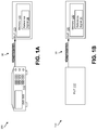
- FIG. 1A illustrates an example system to perform an electrical test at a device under test.
- FIG. 1B illustrates another example system to perform an electrical test at a device under test.
- FIG. 1C illustrates an example synchronization between a test signal and a reference signal.
- FIG. 2 illustrates an example system for performing an electrical test at a device under test.
- FIG. 3 illustrates one more example system for performing an electrical test at a device under test.
- FIG. 4 illustrates an example method for executing an electrical test at a device under test.
- FIG. 5A illustrates an example reference signal stored in a memory at a device under test.
- FIG. 5B illustrates storing of word-lines of a reference signal in a memory of a device under test.
- FIG. 5C illustrates blocks including portions of phase-shifted versions of a sequence stored in a memory of a device under test.
- An example device which can be referred to as a device under test (DUT), configured to perform electrical self-testing is described herein.
- the testing may be performed to determine whether the device has the desired performance characteristics.
- the device may receive a test signal from test equipment and the received test signal may be compared with a reference signal stored at the device. The comparison may be used to determine whether the device has the desired performance characteristics.
- the device may include a receiver, a processor, and a memory.
- the receiver may receive a test signal from test equipment (e.g., a device which can generate a test signal).
- the receiver converts the test signal into a digital test signal (e.g., bit stream) and stores the bit stream in the memory.
- a digital test signal e.g., bit stream
- the receiver may compare the bit stream with a reference signal stored in the memory.
- the reference signal may include a plurality of phase-shifted versions of a sequence which may be, for example, a pseudorandom binary sequence (PRBS).
- PRBS pseudorandom binary sequence
- the comparing determines whether bits of the bit stream match with corresponding bits of the reference signal to determine whether the bit stream was correctly received at the receiver.
- the total number of bits of the bit stream that were not received correctly (e.g. received in error, number of mismatched bits, etc.) at the receiver may be used to determine a test result.
- the test result may be used then to determine whether the test result satisfies a condition, for example, by comparing to a threshold value associated with the test result.
- the test result may be used to determine whether the device passes a bit error rate (BER) test or the BER satisfies BER threshold value to determine whether the device has the desired performance characteristics.
- BER bit error rate
- the implementations described herein may be advantageous over, for example, a system that requires an external trigger event, exchanging of test parameters, additional test equipment, and so forth.
- the self-testing mechanisms described herein can eliminate test equipment and/or measurement capabilities and/or may obviate additional circuitry to implement the testing on-chip.
- the mechanisms described herein may provide common metrics for DUT characterization, production, and in-the-field application. The metrics may be computed in real-time with minimal processor load, without any external triggers, and with minimal RF interference.
- the other advantages of the implementations described herein may include, for example, organizing of subsequences in a memory so that the memory can read linearly without any further data manipulations, achieving real-time operations with minimal processing resources, absence of any feedback mechanism (clock or data signals) to the transmitter as the metrics are computed locally (for example, on chip), and the ability to test two devices together in the field with one device being used as a transmitter and the other device being used as the receiver and computing the metrics.
- FIG. 1A illustrates an example system 100 with a DUT 120 configured to perform an electrical test (e.g., BER, PER, etc.), for example, on-chip, in response to receiving a test signal 30 (e.g., a radio frequency (RF) signal, known data, a known sequence, etc.) from test equipment 110 (e.g., a test signal generator).
- a test signal 30 e.g., a radio frequency (RF) signal, known data, a known sequence, etc.
- RF radio frequency
- the DUT 120 may include a memory 130 which may have reference signal 34 stored in the memory 130 .
- the DUT 120 may compare the test signal 30 received from the test equipment 110 with the reference signal 34 stored in the memory 130 to determine whether the DUT 110 satisfies the desired performance characteristics.
- the DUT 110 may include a module to produce the test signal 30 .
- bit error rate BER
- PER packet error rate
- the BER may be generally defined as the number of bits received in error (e.g., bit errors) divided by the total number of received bits.
- the PER may be generally defined as number of error packets divided by the total number of received packets.
- the BER may be computed on-chip in the DUT 120 instead of being computed externally due to numerous disadvantages of computing externally. For instance, if the BER were computed externally instead of on-chip in the DUT 120 , demodulated clock and data bit streams would be sent back (e.g., feedback mechanism) from the DUT 120 to the test equipment 110 (or another computing device) to compute the number of erroneous bits. In such a test configuration, the BER test may rely on a specific signal generator with clock and data inputs. In addition, the demodulated clock and data bits can generate toggling activity on DUT pads that interfere with the input signal and cause artificial sensitivity degradation which is pad voltage dependent. Moreover, possible reflections on the clock and data lines can cause artificial degradation, especially on test equipment that is automated.
- the DUT 120 may be, or may include, an on-chip receiver sensitivity test for use in an integrated transceiver (e.g., radio frequency (RF) transceiver).
- the mechanism of the DUT 120 described herein may obviate the need to use test equipment with BER measurement capabilities or may obviate additional circuitry to realize the test mechanism on-chip.
- the DUT 120 described herein may include on-chip test signal processing or reference signal generation.
- the mechanisms described herein may be software-based and may be implemented using a reprogrammable processing unit included in the DUT 120 .
- the mechanisms described herein may be implemented in the hardware of the DUT 120 . The results of the testing may determine whether the sensitivity requirements of the receiver are satisfied or met.
- the test equipment 110 may be any RF capable device, and may be replaced with another device, as shown for example, in FIG. 1B .
- the test signal 30 may be synchronized with the reference signal 34 for properly comparing the test signal 30 with the reference signal 34 .
- the synchronization may be needed as the phase of the test signal (e.g., starting of the test signal) may be unknown, as described below in detail in reference to FIG. 1B .
- FIG. 1B illustrates another example system 150 to perform an electrical test at a device under test.
- the test equipment may be another DUT, for example, DUT 112 .
- DUT 112 two devices (e.g., DUT 112 and DUT 120 ) may be tested against each other with a first device, e.g., DUT 112 , generating a test signal (e.g., test signal 30 ) and a second device, e.g., DUT 120 , measuring sensitivity (e.g., whether the DUT 120 satisfies the desired performance characteristics).
- sensitivity e.g., whether the DUT 120 satisfies the desired performance characteristics.
- This may be performed in the field to validate, for example, integration of a DUT into a system or a network, or to measure the quality of reception in a given environment (e.g., to measure quality of a Bluetooth low energy (BLE) link between two devices).
- BLE Bluetooth low energy
- the DUT 120 may generate the test signal and the DUT 112 may measure sensitivity.
- FIG. 1C illustrates an example synchronization 160 between a test signal and a reference signal.
- the test signal 32 may be in a continuous loop (e.g., 30 A, 30 B, 30 C, 30 D, etc.) and the phase of the test signal 30 may be unknown.
- the starting point of the test signal 30 may be unknown.
- the DUT 120 needs knowledge of the starting point of the test signal 30 for performing a bitwise (e.g., bit-by-bit) comparison between the test signal 30 and the reference signal 34 . In the absence of such information, the DUT 120 may perform synchronization between the test signal 30 and the reference signal 34 prior to comparison.
- the test signal 30 may be in a continuous loop and the reference signal 34 may include a sequence, e.g., a plurality of sequences (e.g., sequence 0, sequence 1, . . . , sequence N).
- the DUT 120 may perform a correlation between the test signal 30 (or digital version of the test signal 30 ) and the reference signal 34 .
- the DUT 120 may perform correlation between the test signal 30 (e.g., 30 A, 30 B, 30 C, 30 D, etc. which is a repetition of the test signal 30 ) and the sequences (e.g., sequence 0, sequence 1, . . .
- sequence N of the reference signal 34 to find a match, as shown, for example, at 29 A and 29 B. That is, 29 A and 29 B may show the start and end points in the bit stream where there is phase match between the test signal 30 (being repeated) and a sequence (e.g., sequence 10) of the reference signal 34 .
- the DUT 120 finds a match between the test signal 30 and a sequence of the reference signal 34 (e.g., correlation is maximum)
- the test signal 30 and the reference signal 34 may be synchronized at the matching word-line address location.
- the test signal 30 may be in a continuous loop.
- the reference signal 34 may be a pre-defined finite sequence, for example, a PRBS9 which may include all possible phase-shifted versions of a sequence (for a total of 32 sequences), and the sequence may be the same signal as the test signal 30 .
- Each sequence may include 15 or 16 subsequences resulting in a total of 511 possible subsequences or phases for the reference signal.
- the DUT 120 may perform a correlation between the test signal 30 (or digital version of the test signal 30 ) and the various sequences of the reference signal 34 . For instance, the DUT 120 may perform correlation between the test signal 30 (e.g., 30 A, 30 B, 30 C, 30 D, etc.
- 29 A and 29 B may show the start and end points in the bit stream where there phases match between the test signal 30 (being repeated) and (the sequence 29 of) the reference signal 34 .
- the test signal 30 and the reference signal 34 may be synchronized at the matching word-line address location.
- the correlation may be computed over a subsequence instead of a sequence due to properties of PRBS9 and the low BER target (e.g., 10 ⁇ 3 ). Additional details on example synchronization processes are described in reference to at least FIGS. 5A-5C .
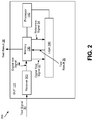
- FIG. 2 illustrates an example system 200 for performing an electrical test at the DUT (e.g., DUT 120 ).
- the DUT 120 shown in FIG. 2 can be an example of the DUT illustrated in, for example, FIG. 1A .
- the electrical test may be a BER test for determining whether a receiver 302 (e.g., a RF receiver) of the DUT 120 satisfies a test condition, e.g., threshold sensitivity requirements.
- a test condition e.g., threshold sensitivity requirements.
- the DUT 120 may include a processor 120 , the memory 130 , a receiver 302 , and/or other components such as a logic operations component, e.g., logic 380 , for performing logic operations.
- the memory 130 is also referred to as a DUT memory, device memory, or a DUT memory portion.
- the receiver 302 of the DUT 120 may receive the test signal 30 from test equipment (e.g., test equipment 110 ), as shown in FIG. 1 .
- the test signal 30 may be a known signal, for example, a known data or a sequence (e.g., a pseudorandom binary sequence (PRBS), PRBS 9).
- PRBS pseudorandom binary sequence
- the receiver 302 may convert the test signal 30 into a digital test signal 32 .
- the digital test signal 32 may be a bit stream (e.g., stream of bits) which is stored in a memory.
- the memory may be a portion of the memory 130 or a local first-in first-out (FIFO) memory of the receiver 302 .
- the memory used for storing the digital test signal 32 is also referred to as a receiver memory or a receiver memory portion.
- the DUT 120 compares the digital test signal 32 to the reference signal 34 for determining whether the receiver 302 of the DUT 120 satisfies threshold sensitivity requirements.
- the reference signal 34 may be a known sequence, e.g., same as the test signal 30 , which may be pre-generated and stored in the memory 130 for processing with the digital test signal 32 using logic 380 .
- the reference signal 34 may be a pseudorandom binary sequence (PRBS), e.g., PRBS9.
- the logic 380 may be configured to perform a test (e.g., BER test) at the DUT 120 to determine whether the test is successful (e.g., whether the receiver 302 of the DUT 120 satisfies threshold sensitivity requirements) and displays the test result 36 .
- a test e.g., BER test
- the digital test signal 32 that is converted from the test signal 30 (e.g., a known sequence) is compared to the sequence (e.g., same sequence) that is locally stored to determine whether certain conditions are met, for example, whether bit error ratio based on the comparison between the digital test signal 32 and the reference signal 34 them satisfies a certain condition (e.g., satisfies sensitivity requirements).
- a known signal that is received over a wireless medium at the receiver 302 is compared with the known signal (or phase shifted versions of the known signal) stored at the device to determine if the known signal was correctly received, and therefore, whether the receiver meets the sensitivity requirements.
- FIG. 3 illustrates an example system 300 for performing a test at a DUT (e.g., DUT 120 ).
- the DUT 120 may include receiver 302 , synchronization logic 380 (can be referred to as logic), and a memory 130 .
- the receiver 302 may include at least an antenna 310 , a filter 315 , a low noise amplifier (LNA) 320 , a voltage controlled oscillator (VCO) 330 (e.g., a local oscillator), a mixer 340 (e.g., an ideal mixer, a multiplier), an automatic gain control 350 , an analog to digital converter 360 , or a memory 370 for receiving a test signal 30 , converting the test signal 30 to the digital test signal 32 , storing the digital test signal 32 in the memory 370 , or identifying when a pre-defined number of bits are available in the memory 370 .
- LNA low noise amplifier
- VCO voltage controlled oscillator
- the identifying may be based, for example, on an interrupt (a system interrupt, a direct memory access request, etc.)
- the receiver 302 may include different components than shown in FIG. 3 .
- the receiver 302 may be configured to demodulate the test signal 30 and generate a bit stream (e.g., digital test signal 32 ), and for example, at a rate of 1 Mb/s for a BLE link.
- the receiver 302 may be configured with a reprogrammable CPU (not shown in FIG. 3 ) and some memory (e.g., memory 370 , which may be a local FIFO memory at the receiver 302 or a portion of the memory 130 ) to perform the operations described herein.
- the receiver 302 may be configured to receive the test signal 30 via the antenna 310 and is configured to produce the digital test signal 32 that may be stored in the memory 370 .
- the memory 370 may be a FIFO memory of the receiver 302 or a portion of the memory 130 .
- the reference signal 34 may be stored in memory 392 , which may be a part of the memory 130 in some implementations, and may be processed with the digital test signal 32 using logic 380 .
- the reference signal 34 may be a pseudorandom binary sequence (PRBS), e.g., PRBS9.
- PRBS pseudorandom binary sequence
- the logic 380 may include XOR comparison logic 382 , summation logic 384 , or result logic 386 .
- the XOR comparison logic 382 compares the digital test signal 32 with the reference signal 34 , e.g., on a per-bit basis, and may produce a logic value, e.g., a logic high value or a value of 1, if the comparison results in a mismatch (bits do not match). For instance, a value of 1 may be produced in the event a bit of the digital test signal 32 does not match with a corresponding bit of the reference signal 34 (e.g., corresponding bit of the corresponding sequence of the reference signal). A value of 0 may be produced in the event a bit of the digital test signal 32 matches with a corresponding bit of the reference signal 34 .
- the summation logic 384 may be configured to add total number of unmatched bits (or matched bits) based on the comparison performed using the XOR comparison logic 382 .
- the result logic 386 may be configured to determine whether the test result 36 satisfies the condition based on a test criterion configured at the device, the test criterion based on the total number of bits that failed to match.
- the test criterion e.g., which may be pre-defined by the manufacturer of the chip or the DUT 120
- the test result 36 may be used to determine whether the receiver 302 of the DUT 120 passed the test (e.g., satisfied threshold sensitivity requirements).
- the result logic 386 may determine the test result 36 , e.g., BER, and may determine whether the BER satisfies the threshold hold sensitivity requirements.
- the test result may be stored in the memory 394 which is a portion of the memory 130 .
- the logic 380 may include synchronization logic 388 .
- the logic 388 may be configured to facilitate synchronization between the digital test signal 32 and the reference signal 34 . Without proper synchronization between the digital test signal 32 and the reference signal 34 , an accurate comparison of the digital test signal 32 and the reference signal 34 cannot be performed in a desirable fashion.
- the test signal 30 may be in a continuous loop and processed by the receiver 302 continuously resulting in the need for synchronization between the digital test signal 32 and reference signal 34 .
- the receiver 302 may be configured to continuously receive a looped version of a known test signal or code modulated as the test signal 30 .
- the reference signal 34 may be pre-computed (e.g., pre-generated) and stored in the memory 392 prior to the synchronization process as the generation of the reference signal 34 may consume significant processing resources. Additional details on the synchronization process are described in detail at least in reference to FIGS. 5A-5C .
- the system or mechanism shown in FIG. 3 may be used to implement a BER meter in software (e.g., software BER meter) directly on-chip of the DUT 120 .
- the software may be configured to compute the BER in real-time with reduced (e.g., minimal) processing load, for example, in part, due to pre-computing (e.g., pre-generating) the reference signal 34 and storing the reference signal 34 in the memory 392 .
- the reference signal 34 which may be pre-generated may include a plurality of phase-shifted versions of a sequence that may be used to automatically synchronize the digital test signal 32 with the reference signal 34 , thus obviating the need for any external trigger or external synchronization mechanism.
- the processor 120 may execute logic 380 and load the digital test signal 32 from the memory 370 , the reference signal 34 , and compute the correlation between the digital test signal 32 and the reference signal 34 using the logic 380 .
- the comparison e.g., correlation
- each resulting bit being set to a high value may correspond to an erroneously processed (e.g., received) bit.
- the logic 382 may be configured to compute the amount of ones (1s) of the XOR operation.
- an algorithm e.g., in logic 380 with a complexity proportional to the number of ones may be used.
- the logic 380 may be configured to detect a scenario where there are no mismatches between the digital test signal 32 and the reference signal 34 . In such situations, the calculation of an error rate will not be completed because it is not needed. If there is a mismatch between the digital test signal and the reference signal, the calculation of an error rate may be triggered.
- the test result 36 of the result operation may be defined (e.g., accumulated, collected, calculated) over, for example, a pre-defined amount of data and stored in the memory 394 .
- the test result 36 may be a BER calculated as the ratio between the number of erroneously received bits and the total amount of received bits.
- processing illustrated in FIG. 3 may be performed in software, hardware, firmware, or a combination thereof. Accordingly, all, or a portion, of the processing may be executed using, for example, one or more general purpose processors and/or one or more memories.
- FIG. 4 illustrates a flowchart 400 of an example method of executing an electrical test at a DUT (e.g., at DUT 120 as shown in FIGS. 1A-3 ).
- a DUT e.g., at DUT 120 as shown in FIGS. 1A-3 .
- at least some portions of the method can be performed using a non-transitory computer-readable storage medium storing instructions that when executed cause a processor to perform the method.
- the DUT receives a test signal.
- the DUT 120 or the receiver 302 may receive the test signal 30 , via the antenna 310 , from the test equipment 110 .
- the test signal 30 may be a RF test signal and the receiver 302 may be a RF receiver configured to receive the test signal 30 .
- the test signal 30 may be a known data signal, e.g., a sequence.
- the DUT may convert the test signal into a digital test signal and store the digital test signal in a receiver memory portion, the digital test signal being a bit stream generated from the test signal.
- the DUT 310 , the receiver 302 , or the analog to digital converter 360 may convert the test signal 30 into a digital test signal 32 (e.g., bit stream, sequence of bits, etc.) and store the digital test signal 32 in a receiver memory portion (e.g., memory 370 ).
- the receiver memory portion 370 may be a local memory at the receiver 302 (e.g., FIFO memory at the receiver 302 ) or a portion of the memory 130 .
- the digital test signal 32 may be temporarily stored in the memory, for example, as 8, 16, or 32 bit data.
- the DUT may identify when a pre-defined number of bits of the bit stream are available in the receiver memory portion.
- the DUT 100 or the receiver 302 may identify when a pre-defined number of bits of the bit stream are available in the receiver memory portion 370 .
- the identifying may be based on an interrupt, for example, a system interrupt, a direct memory access request, etc.
- the DUT 100 may perform, in response to the identifying, a logic operation on the bit stream and a reference signal, and generate a test result based on the logic operation.
- the DUT 100 or the processor 140 may perform a logic operation on the bit stream (e.g., digital test signal 32 ) and the reference signal 34 , and may generate the test result 36 based on the logic operation.
- the DUT may determine whether the test result satisfies a condition. For example, in one implementation, the DUT 100 or the processor 140 may determine whether the test result 36 satisfies a condition, e.g., threshold sensitivity requirements. In some implementations, the DUT 120 or the processor 140 may determine whether BER test results satisfies threshold sensitivity requirements. The DUT 120 or the processor 140 may determine that the BER test result satisfies the condition if the BER is below the BER threshold sensitivity requirement of the receiver 302 .
- a condition e.g., threshold sensitivity requirements.
- the DUT 120 or the processor 140 may determine whether BER test results satisfies threshold sensitivity requirements. The DUT 120 or the processor 140 may determine that the BER test result satisfies the condition if the BER is below the BER threshold sensitivity requirement of the receiver 302 .
- the DUT may synchronize the digital test signal with the reference signal prior to performing of the logic operation.
- the DUT 120 or the processor 140 may synchronize the digital test signal 32 with the reference signal 34 prior to performing the logic operation to efficiently perform the logic operation described above in reference to block 440 .
- the reference signal 34 may include a plurality of phased-shifted versions of a sequence (e.g., PRBS9).
- the reference signal 34 may be pre-generated and stored in the memory 392 in a word aligned manner to improve speed or efficiency of the synchronization or logic operations which are described below in detail in reference to at least FIGS. 5A-5C .
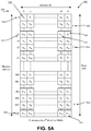
- FIG. 5A illustrates an example reference signal 34 , which includes multiple phase-shifted versions of a sequence, stored in a memory (e.g., memory 392 ).
- the reference signal 34 may include a plurality of consecutive phase-shifted versions of a sequence (referred to as a plurality of sequences) which may be generated from the sequence using, for example, a shift register.
- each sequence may be a PRBS, for example, PRBS9, which has a length of 511 bits.
- the plurality of sequences (for example, 8, 16, 24, 32, etc. sequences, which may depend on the memory structure), to accommodate the length of PRBS9, may be pre-computed or pre-generated (e.g., externally, on-chip, etc.) and stored (e.g., loaded) in the memory 392 to save time or conserve processing resources.
- consecutive sequences may be stored in a row in the memory 392 .
- consecutive sequences may be stored in the memory 392 in a way (e.g., in rows) such that a last subsequence is word aligned (or memory word aligned).
- the first sequence which may be referred to as sequence 0 ( 510 ) may be stored in the memory starting at bit 0 (P 0 ) 530 of memory address 0 ( 520 ) and ending at memory bit 30 (P 510 ) 532 of memory address 15 ( 522 ).
- the last subsequence 522 of sequence 0 ( 510 ) may be word aligned with a following sequence ( 512 ) starting at memory bit 31 (P 0 ) 534 of memory address 15 ( 522 ).
- the last subsequence of a sequence may be memory word aligned with the following sequence, and applies to any sequence length and to any memory.
- the last bit (bit 31 ) of the last memory address (address 510 ) stores P 510 . That is, consecutive sequences are stored in a row until the condition (the last bit of the last memory address storing P 510 ) is satisfied.
- This mechanism allows for efficient comparison, e.g., word-by-word comparison or 32-bit comparison for detecting mismatched bits to compute error rates for determining metrics, e.g., BER, PER, etc.
- the memory footprint may be reduced to 511 or 1022 bytes by using 8 or 16-bit memory addresses, respectively, which may result in higher processing loads (e.g., additional logical shift operations).
- the plurality of phase-shifted versions of the sequence are stored with last subsequences of the plurality of phase-shifted versions memory such that they are word, or half-word, or byte aligned.
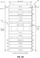
- FIG. 5B illustrates storing of word-lines of a reference signal 34 in a memory (e.g., memory 392 ) based on the example implementation of FIG. 5A .
- the first word-line 540 stored at memory address 0 ( 520 ) includes bits shown as [P0:P31] 540 .
- a word-line 542 stored at memory address 31 ( 526 ) includes bits shown as [P481:P510; P0:P1] which includes end portion of one sequence, sequence 0 (e.g., [P481:P510]) and beginning portion, e.g., [P0:P1], of the following sequence, sequence 1 ( 512 ).
- a word-line at address memory 510 includes bits [P479: P510], where P510 being the last bit of the PRBS9 sequence occupies the last bit of the last address.
- consecutive phased-shifted versions of PRBS9 may be stored in a row (e.g., in a loop fashion) until the last bit of the reference signal 534 (e.g., P510 in FIG. 5A ) coincides with the last bit (for example, bit 31 ) of memory address 510 ( 524 ).
- the memory may be read linearly. That is, after reading memory address 510 ( 524 ) subsequence [P479:P510], the pointer may be reinitialized to the memory address 0 (subsequence [P0:P31]) to ensure continuity of the sequence (or code). This is due to the length of PRBS9 (e.g., 511 bits) which is not an integer multiple of 32.
- the example mechanism described above aligns the PRBS9 with the memory even though the length of the PRBS9 is 511 bits.
- FIG. 5C illustrates blocks including portions of phase-shifted versions of a sequence 34 that are stored in the memory 392 as illustrated in FIGS. 5A-5B .
- each block may include portions of at least two sequences of a PRBS (e.g., PRBS9).
- PRBS e.g., PRBS9
- the PRBS9 may be stored using, for example, 32-bit wide combinations, so that all the plurality of sequences of the PRBS9 are stored in the memory 392 . This may allow for relatively less-complex comparison of the digital test signal 32 with the reference signal 34 on a word-line basis (e.g., 32-bit word comparison).
- the synchronization between the digital test signal 32 and the PRBS9 (e.g., multiple phase-shifted versions of the reference signal 34 shown in FIG. 5A ) may be performed in multiple ways.
- the synchronization of the digital test signal 32 with the reference signal 34 may be performed prior to the comparison.
- the data phase of the digital test signal 32 may be unknown as the test signal 30 is being continuously looped.
- the synchronization may include searching all possible phases of the PRBS9 (e.g., 511 phase shifts) and performing the synchronization when the correlation between the digital test signal 32 and the PRBS9 satisfies a threshold condition (e.g., correlation is maximized).
- the correlation may be computed over a subsequence (e.g., 520 , 522 , etc.) of a sequence of the PRBS9.
- the correlation length e.g., number of bits used for correlation
- a 32-bit portion of the digital test signal 32 may be compared with word-lines (e.g., 32 bits each) stored in the memory 392 until a match is found.
- the digital test signal 32 may be synchronized with the memory 392 at the matching word-line address location.
- subsequent 32-bit word-lines of the digital test signal 32 may be compared with the subsequently addressed word-lines stored in the memory 392 .
- the receiver 302 may have basic packet handling functionalities capable of detecting a pre-defined pattern (e.g., for detecting a 32-bit sync word of a received Bluetooth LE packet).
- a pre-defined pattern e.g., for detecting a 32-bit sync word of a received Bluetooth LE packet.
- the digital test signal 32 stored in the receiver memory 370 e.g., FIFO memory 370 of the receiver 302
- the digital test signal 32 stored in the receiver memory 370 may be automatically aligned with the bit P 0 of the PRBS9 sequence.
- the memory pointer of the PRBS9 sequence in response to synchronization being achieved (e.g., after performing a search over all (or a subset of) the possible phases), may be initialized at the memory address location with content that matches the digital test signal. In some implementations, if needed, the pointer is adjusted in order to compensate for the time spent during the search process (time is translated into an equivalent phase shift). In some implementations, the storing of consecutive versions in a row, as described above in reference to FIGS. 5A and 5B , applies to FIG. 5C as well where subsequence [P479:P510] may be used as a reference so that the next subsequence read is [P0:P31] at memory address 0 ( 520 ).
- the pointer may be initialized to the first address. For each new received data, the memory pointer may be linearly incremented until it reaches the 2 9 ⁇ 2 memory address. In some implementations, the pointer may be reinitialized to the first address in order to ensure the sequence continuity. In some implementations, the tracking between the PRBS9 sequence and the data can be efficient since the correlations may be computed on native 32-bit operands that are read linearly from the memory without any logical shift operations.
- a non-transitory computer-readable storage medium may be configured to store instructions that when executed cause a processor to perform a process.
- the process may include receiving, at a device under test (DUT), a test signal, converting, by the DUT, the test signal into a digital test signal and storing the digital test signal in a receiver memory portion, the digital test signal being a bit stream generated from the test signal, identifying, by the DUT, when a pre-defined number of bits of the bit stream are available in the receiver memory portion.
- DUT device under test
- the process may further include performing, by the DUT, in response to the identifying, a logic operation on the bit stream and a reference signal, and generating a test result based on the logic operation, the reference signal including a plurality of phase-shifted versions of a sequence, and the reference signal pre-generated and stored in a DUT memory portion; and determining, by the DUT, whether the test result satisfies a condition.
- a singular form may, unless definitely indicating a particular case in terms of the context, include a plural form.
- Spatially relative terms e.g., over, above, upper, under, beneath, below, lower, and so forth
- the relative terms above and below can, respectively, include vertically above and vertically below.
- the term adjacent can include laterally adjacent to or horizontally adjacent to.
- Implementations of the various techniques described herein may be implemented in (e.g., included in) digital electronic circuitry, or in computer hardware, firmware, software, or in combinations of them. Implementations may implemented as a computer program product, i.e., a computer program tangibly embodied in an information carrier, e.g., in a machine readable storage device (computer-readable medium) or in a propagated signal, for processing by, or to control the operation of, data processing apparatus, e.g., a programmable processor, a computer, or multiple computers.
- a computer program product i.e., a computer program tangibly embodied in an information carrier, e.g., in a machine readable storage device (computer-readable medium) or in a propagated signal, for processing by, or to control the operation of, data processing apparatus, e.g., a programmable processor, a computer, or multiple computers.
- a computer program such as the computer program(s) described above, can be written in any form of programming language, including compiled or interpreted languages, and can be deployed in any form, including as a stand alone program or as a module, component, subroutine, or other unit suitable for use in a computing environment.
- a computer program can be deployed to be processed on one computer or on multiple computers at one site or distributed across multiple sites and interconnected by a communication network.
- Method steps may be performed by one or more programmable processors executing a computer program to perform functions by operating on input data and generating output. Method steps also may be performed by, and an apparatus may be implemented as, special purpose logic circuitry, e.g., an FPGA (field programmable gate array) or an ASIC (application specific integrated circuit).
- FPGA field programmable gate array
- ASIC application specific integrated circuit
- processors suitable for the processing of a computer program include, by way of example, both general and special purpose microprocessors, and any one or more processors of any kind of digital computer.
- a processor will receive instructions and data from a read only memory or a random access memory or both.
- Elements of a computer may include at least one processor for executing instructions and one or more memory devices for storing instructions and data.
- a computer also may include, or be operatively coupled to receive data from or transfer data to, or both, one or more mass storage devices for storing data, e.g., magnetic, magneto optical disks, or optical disks.
- Information carriers suitable for embodying computer program instructions and data include all forms of non volatile memory, including by way of example semiconductor memory devices, e.g., EPROM, EEPROM, and flash memory devices; magnetic disks, e.g., internal hard disks or removable disks; magneto optical disks; and CD ROM and DVD-ROM disks.
- semiconductor memory devices e.g., EPROM, EEPROM, and flash memory devices
- magnetic disks e.g., internal hard disks or removable disks
- magneto optical disks e.g., CD ROM and DVD-ROM disks.
- the processor and the memory may be supplemented by, or incorporated in special purpose logic circuitry.
Landscapes
- Engineering & Computer Science (AREA)
- General Engineering & Computer Science (AREA)
- Physics & Mathematics (AREA)
- General Physics & Mathematics (AREA)
- Theoretical Computer Science (AREA)
- Quality & Reliability (AREA)
- Computer Hardware Design (AREA)
- Nonlinear Science (AREA)
- Tests Of Electronic Circuits (AREA)
Abstract
Description
Claims (17)
Priority Applications (1)
| Application Number | Priority Date | Filing Date | Title |
|---|---|---|---|
| US15/895,784 US10551437B2 (en) | 2017-07-20 | 2018-02-13 | Error rate meter included in a semiconductor die |
Applications Claiming Priority (2)
| Application Number | Priority Date | Filing Date | Title |
|---|---|---|---|
| US201762534775P | 2017-07-20 | 2017-07-20 | |
| US15/895,784 US10551437B2 (en) | 2017-07-20 | 2018-02-13 | Error rate meter included in a semiconductor die |
Publications (2)
| Publication Number | Publication Date |
|---|---|
| US20190025372A1 US20190025372A1 (en) | 2019-01-24 |
| US10551437B2 true US10551437B2 (en) | 2020-02-04 |
Family
ID=65018984
Family Applications (1)
| Application Number | Title | Priority Date | Filing Date |
|---|---|---|---|
| US15/895,784 Active US10551437B2 (en) | 2017-07-20 | 2018-02-13 | Error rate meter included in a semiconductor die |
Country Status (1)
| Country | Link |
|---|---|
| US (1) | US10551437B2 (en) |
Families Citing this family (4)
| Publication number | Priority date | Publication date | Assignee | Title |
|---|---|---|---|---|
| US10735115B2 (en) * | 2018-07-31 | 2020-08-04 | Nxp B.V. | Method and system to enhance accuracy and resolution of system integrated scope using calibration data |
| US10396912B1 (en) | 2018-08-31 | 2019-08-27 | Nxp B.V. | Method and system for a subsampling based system integrated scope to enhance sample rate and resolution |
| US11598804B2 (en) * | 2019-03-22 | 2023-03-07 | Intel Corporation | Debug tool for test instruments coupled to a device under test |
| JP7227189B2 (en) * | 2020-07-01 | 2023-02-21 | アンリツ株式会社 | Mobile terminal test equipment and mobile terminal test method |
Citations (11)
| Publication number | Priority date | Publication date | Assignee | Title |
|---|---|---|---|---|
| US20030142737A1 (en) | 2002-01-29 | 2003-07-31 | Tony Tarng | Fast bit-error-rate (BER) test |
| US20040148580A1 (en) | 2003-01-17 | 2004-07-29 | Texas Instruments Incorporated | On-chip receiver sensitivity test mechanism |
| US20040268190A1 (en) * | 2003-05-19 | 2004-12-30 | International Business Machines Corporation | Adjusting parameters of a serial link |
| US20070014341A1 (en) | 2005-07-12 | 2007-01-18 | Graham Rowse | Optimized RFID/NFC BER testing |
| US20080016422A1 (en) * | 2006-07-11 | 2008-01-17 | Advantest Corporation | Test apparatus, shift amount measuring apparatus, shift amount measuring method and diagnostic method |
| US20090115443A1 (en) * | 2007-11-01 | 2009-05-07 | Kingtiger Technology (Canada) Inc. | System and method for testing integrated circuit modules comprising a plurality of integrated circuit devices |
| US20090119053A1 (en) * | 2004-11-09 | 2009-05-07 | Wayne Tseng | Serial Interface Device Built-In Self Test |
| US7574633B2 (en) * | 2006-07-12 | 2009-08-11 | Advantest Corporation | Test apparatus, adjustment method and recording medium |
| US20100312507A1 (en) * | 2007-04-25 | 2010-12-09 | Advantest Corporation | Test apparatus |
| US20110128044A1 (en) * | 2008-07-09 | 2011-06-02 | Advantest Corporation | Test apparatus, test method, and phase shifter |
| US8327206B2 (en) * | 2009-12-19 | 2012-12-04 | Tektronix, Inc. | Blanking primitives masking circuit |
-
2018
- 2018-02-13 US US15/895,784 patent/US10551437B2/en active Active
Patent Citations (12)
| Publication number | Priority date | Publication date | Assignee | Title |
|---|---|---|---|---|
| US20030142737A1 (en) | 2002-01-29 | 2003-07-31 | Tony Tarng | Fast bit-error-rate (BER) test |
| US20040148580A1 (en) | 2003-01-17 | 2004-07-29 | Texas Instruments Incorporated | On-chip receiver sensitivity test mechanism |
| US20040268190A1 (en) * | 2003-05-19 | 2004-12-30 | International Business Machines Corporation | Adjusting parameters of a serial link |
| US20090119053A1 (en) * | 2004-11-09 | 2009-05-07 | Wayne Tseng | Serial Interface Device Built-In Self Test |
| US20070014341A1 (en) | 2005-07-12 | 2007-01-18 | Graham Rowse | Optimized RFID/NFC BER testing |
| US20080016422A1 (en) * | 2006-07-11 | 2008-01-17 | Advantest Corporation | Test apparatus, shift amount measuring apparatus, shift amount measuring method and diagnostic method |
| US7574633B2 (en) * | 2006-07-12 | 2009-08-11 | Advantest Corporation | Test apparatus, adjustment method and recording medium |
| US20100312507A1 (en) * | 2007-04-25 | 2010-12-09 | Advantest Corporation | Test apparatus |
| US20090115443A1 (en) * | 2007-11-01 | 2009-05-07 | Kingtiger Technology (Canada) Inc. | System and method for testing integrated circuit modules comprising a plurality of integrated circuit devices |
| US7757144B2 (en) * | 2007-11-01 | 2010-07-13 | Kingtiger Technology (Canada) Inc. | System and method for testing integrated circuit modules comprising a plurality of integrated circuit devices |
| US20110128044A1 (en) * | 2008-07-09 | 2011-06-02 | Advantest Corporation | Test apparatus, test method, and phase shifter |
| US8327206B2 (en) * | 2009-12-19 | 2012-12-04 | Tektronix, Inc. | Blanking primitives masking circuit |
Also Published As
| Publication number | Publication date |
|---|---|
| US20190025372A1 (en) | 2019-01-24 |
Similar Documents
| Publication | Publication Date | Title |
|---|---|---|
| US10551437B2 (en) | Error rate meter included in a semiconductor die | |
| US9288777B2 (en) | Methods and apparatus for synchronizing clock signals in a wireless system | |
| JP6404467B2 (en) | Duty cycle based timing margining for I / O AC timing | |
| CN102549443B (en) | Programmable protocol generator | |
| US7895485B2 (en) | System and method for testing a packetized memory device | |
| US9255966B2 (en) | Receiver circuit, semiconductor integrated circuit, and test method | |
| KR890702124A (en) | Integrated Circuit Analyzer for Testing Digital Circuits | |
| US9501376B2 (en) | Testing I/O timing defects for high pin count, non-contact interfaces | |
| US20240069591A1 (en) | Clock calibration method and electronic device | |
| US9151800B2 (en) | Chip testing with exclusive OR | |
| US9043662B2 (en) | Double data rate memory physical interface high speed testing using self checking loopback | |
| CN103630720A (en) | Test and measurement instrument with auto-sync for bit-error detection | |
| US10931487B2 (en) | Chip failure detection method and device | |
| US20130036336A1 (en) | Transmitting device, transceiver system, and control method | |
| CN105450433B (en) | Configuration method, the device and system of high-speed serial bus parameter | |
| US9319298B2 (en) | System and method for data packet transceiver testing after signal calibration and power settling to minimize test time | |
| CN113535578B (en) | CTS test method, CTS test device and CTS test equipment | |
| US9837170B2 (en) | Systems and methods for testing performance of memory modules | |
| US10222415B2 (en) | Generic width independent parallel checker for a device under test | |
| CN116991642B (en) | Chip testing method, chip, system and storage medium | |
| US9049020B2 (en) | Circuitry to facilitate testing of serial interfaces | |
| JP2016165064A (en) | Identification device, identification method and program for identification device | |
| US20240133953A1 (en) | Determination device, test system, and generation device | |
| US7552366B2 (en) | Jitter tolerance testing apparatus, systems, and methods | |
| US10171127B2 (en) | Method, system and computer program for synchronizing pseudorandom binary sequence modules |
Legal Events
| Date | Code | Title | Description |
|---|---|---|---|
| FEPP | Fee payment procedure |
Free format text: ENTITY STATUS SET TO UNDISCOUNTED (ORIGINAL EVENT CODE: BIG.); ENTITY STATUS OF PATENT OWNER: LARGE ENTITY |
|
| AS | Assignment |
Owner name: SEMICONDUCTOR COMPONENTS INDUSTRIES, LLC, ARIZONA Free format text: ASSIGNMENT OF ASSIGNORS INTEREST;ASSIGNOR:WAELCHLI, GREGOIRE;REEL/FRAME:044990/0760 Effective date: 20180213 |
|
| STPP | Information on status: patent application and granting procedure in general |
Free format text: DOCKETED NEW CASE - READY FOR EXAMINATION |
|
| AS | Assignment |
Owner name: DEUTSCHE BANK AG NEW YORK BRANCH, AS COLLATERAL AG Free format text: SECURITY INTEREST;ASSIGNOR:SEMICONDUCTOR COMPONENTS INDUSTRIES, LLC;REEL/FRAME:047734/0068 Effective date: 20180426 Owner name: DEUTSCHE BANK AG NEW YORK BRANCH, AS COLLATERAL AGENT, NEW YORK Free format text: SECURITY INTEREST;ASSIGNOR:SEMICONDUCTOR COMPONENTS INDUSTRIES, LLC;REEL/FRAME:047734/0068 Effective date: 20180426 |
|
| STPP | Information on status: patent application and granting procedure in general |
Free format text: NON FINAL ACTION MAILED |
|
| STPP | Information on status: patent application and granting procedure in general |
Free format text: NOTICE OF ALLOWANCE MAILED -- APPLICATION RECEIVED IN OFFICE OF PUBLICATIONS |
|
| STPP | Information on status: patent application and granting procedure in general |
Free format text: PUBLICATIONS -- ISSUE FEE PAYMENT VERIFIED |
|
| STCF | Information on status: patent grant |
Free format text: PATENTED CASE |
|
| AS | Assignment |
Owner name: FAIRCHILD SEMICONDUCTOR CORPORATION, ARIZONA Free format text: RELEASE OF SECURITY INTEREST IN PATENTS RECORDED AT REEL 047734, FRAME 0068;ASSIGNOR:DEUTSCHE BANK AG NEW YORK BRANCH, AS COLLATERAL AGENT;REEL/FRAME:064160/0027 Effective date: 20230622 Owner name: SEMICONDUCTOR COMPONENTS INDUSTRIES, LLC, ARIZONA Free format text: RELEASE OF SECURITY INTEREST IN PATENTS RECORDED AT REEL 047734, FRAME 0068;ASSIGNOR:DEUTSCHE BANK AG NEW YORK BRANCH, AS COLLATERAL AGENT;REEL/FRAME:064160/0027 Effective date: 20230622 |
|
| MAFP | Maintenance fee payment |
Free format text: PAYMENT OF MAINTENANCE FEE, 4TH YEAR, LARGE ENTITY (ORIGINAL EVENT CODE: M1551); ENTITY STATUS OF PATENT OWNER: LARGE ENTITY Year of fee payment: 4 |