TW202324495A - Lithography method - Google Patents
Lithography method Download PDFInfo
- Publication number
- TW202324495A TW202324495A TW110145912A TW110145912A TW202324495A TW 202324495 A TW202324495 A TW 202324495A TW 110145912 A TW110145912 A TW 110145912A TW 110145912 A TW110145912 A TW 110145912A TW 202324495 A TW202324495 A TW 202324495A
- Authority
- TW
- Taiwan
- Prior art keywords
- photomask
- transparent
- holding container
- circuit pattern
- lithography
- Prior art date
Links
Images


Classifications
-
- G—PHYSICS
- G03—PHOTOGRAPHY; CINEMATOGRAPHY; ANALOGOUS TECHNIQUES USING WAVES OTHER THAN OPTICAL WAVES; ELECTROGRAPHY; HOLOGRAPHY
- G03F—PHOTOMECHANICAL PRODUCTION OF TEXTURED OR PATTERNED SURFACES, e.g. FOR PRINTING, FOR PROCESSING OF SEMICONDUCTOR DEVICES; MATERIALS THEREFOR; ORIGINALS THEREFOR; APPARATUS SPECIALLY ADAPTED THEREFOR
- G03F1/00—Originals for photomechanical production of textured or patterned surfaces, e.g., masks, photo-masks, reticles; Mask blanks or pellicles therefor; Containers specially adapted therefor; Preparation thereof
- G03F1/66—Containers specially adapted for masks, mask blanks or pellicles; Preparation thereof
-
- G—PHYSICS
- G03—PHOTOGRAPHY; CINEMATOGRAPHY; ANALOGOUS TECHNIQUES USING WAVES OTHER THAN OPTICAL WAVES; ELECTROGRAPHY; HOLOGRAPHY
- G03F—PHOTOMECHANICAL PRODUCTION OF TEXTURED OR PATTERNED SURFACES, e.g. FOR PRINTING, FOR PROCESSING OF SEMICONDUCTOR DEVICES; MATERIALS THEREFOR; ORIGINALS THEREFOR; APPARATUS SPECIALLY ADAPTED THEREFOR
- G03F1/00—Originals for photomechanical production of textured or patterned surfaces, e.g., masks, photo-masks, reticles; Mask blanks or pellicles therefor; Containers specially adapted therefor; Preparation thereof
- G03F1/52—Reflectors
-
- G—PHYSICS
- G03—PHOTOGRAPHY; CINEMATOGRAPHY; ANALOGOUS TECHNIQUES USING WAVES OTHER THAN OPTICAL WAVES; ELECTROGRAPHY; HOLOGRAPHY
- G03F—PHOTOMECHANICAL PRODUCTION OF TEXTURED OR PATTERNED SURFACES, e.g. FOR PRINTING, FOR PROCESSING OF SEMICONDUCTOR DEVICES; MATERIALS THEREFOR; ORIGINALS THEREFOR; APPARATUS SPECIALLY ADAPTED THEREFOR
- G03F7/00—Photomechanical, e.g. photolithographic, production of textured or patterned surfaces, e.g. printing surfaces; Materials therefor, e.g. comprising photoresists; Apparatus specially adapted therefor
- G03F7/20—Exposure; Apparatus therefor
- G03F7/2002—Exposure; Apparatus therefor with visible light or UV light, through an original having an opaque pattern on a transparent support, e.g. film printing, projection printing; by reflection of visible or UV light from an original such as a printed image
-
- G—PHYSICS
- G03—PHOTOGRAPHY; CINEMATOGRAPHY; ANALOGOUS TECHNIQUES USING WAVES OTHER THAN OPTICAL WAVES; ELECTROGRAPHY; HOLOGRAPHY
- G03F—PHOTOMECHANICAL PRODUCTION OF TEXTURED OR PATTERNED SURFACES, e.g. FOR PRINTING, FOR PROCESSING OF SEMICONDUCTOR DEVICES; MATERIALS THEREFOR; ORIGINALS THEREFOR; APPARATUS SPECIALLY ADAPTED THEREFOR
- G03F7/00—Photomechanical, e.g. photolithographic, production of textured or patterned surfaces, e.g. printing surfaces; Materials therefor, e.g. comprising photoresists; Apparatus specially adapted therefor
- G03F7/70—Microphotolithographic exposure; Apparatus therefor
- G03F7/708—Construction of apparatus, e.g. environment aspects, hygiene aspects or materials
- G03F7/70908—Hygiene, e.g. preventing apparatus pollution, mitigating effect of pollution or removing pollutants from apparatus
- G03F7/70916—Pollution mitigation, i.e. mitigating effect of contamination or debris, e.g. foil traps
-
- G—PHYSICS
- G03—PHOTOGRAPHY; CINEMATOGRAPHY; ANALOGOUS TECHNIQUES USING WAVES OTHER THAN OPTICAL WAVES; ELECTROGRAPHY; HOLOGRAPHY
- G03F—PHOTOMECHANICAL PRODUCTION OF TEXTURED OR PATTERNED SURFACES, e.g. FOR PRINTING, FOR PROCESSING OF SEMICONDUCTOR DEVICES; MATERIALS THEREFOR; ORIGINALS THEREFOR; APPARATUS SPECIALLY ADAPTED THEREFOR
- G03F7/00—Photomechanical, e.g. photolithographic, production of textured or patterned surfaces, e.g. printing surfaces; Materials therefor, e.g. comprising photoresists; Apparatus specially adapted therefor
- G03F7/70—Microphotolithographic exposure; Apparatus therefor
- G03F7/708—Construction of apparatus, e.g. environment aspects, hygiene aspects or materials
- G03F7/70983—Optical system protection, e.g. pellicles or removable covers for protection of mask
-
- H10P72/1902—
-
- H10P72/1906—
-
- H10P72/1911—
-
- H10P72/1922—
-
- G—PHYSICS
- G02—OPTICS
- G02B—OPTICAL ELEMENTS, SYSTEMS OR APPARATUS
- G02B7/00—Mountings, adjusting means, or light-tight connections, for optical elements
- G02B7/006—Filter holders
Landscapes
- General Physics & Mathematics (AREA)
- Physics & Mathematics (AREA)
- Public Health (AREA)
- Engineering & Computer Science (AREA)
- Health & Medical Sciences (AREA)
- Epidemiology (AREA)
- Environmental & Geological Engineering (AREA)
- Atmospheric Sciences (AREA)
- Life Sciences & Earth Sciences (AREA)
- Exposure And Positioning Against Photoresist Photosensitive Materials (AREA)
- Preparing Plates And Mask In Photomechanical Process (AREA)
- Condensed Matter Physics & Semiconductors (AREA)
- Manufacturing & Machinery (AREA)
- Computer Hardware Design (AREA)
- Microelectronics & Electronic Packaging (AREA)
- Power Engineering (AREA)
Abstract
Description
本發明隸屬一種微影製程之技術領域,具體而言係一種透微影方法,藉以使光罩能在被保護的狀態下進入微影製程中,以減少光罩表面在微影製程中被污染的機會,能夠提高半導體製程良率。 The present invention belongs to the technical field of a lithography process, specifically a lithography method, so that the photomask can enter the lithography process in a protected state, so as to reduce the pollution of the photomask surface during the lithography process Opportunities to improve semiconductor process yield.
按,電子產品不斷朝向輕薄短小、高頻、高效能等特性發展,使得用於電子產品中的核心半導體元件就需微小化與具有高效能,因此現有半導體元件的電路圖案線徑已由早期的微米級發展至奈米級。而依據目前的半導體元件製造技術,半導體元件的電路圖案是透過微影〔Lithography〕製程將電路圖案轉印至晶圓的表面,具體而言是利用特定波長的光源投射通過光罩〔Photomask〕的方式,將電路圖案轉印至晶圓的表面。為了實現在單位面積上倍增半導體元件的數目,縮小半導體電路的線寬為其主要的技術方案,目前以波長193奈米的深紫外光〔DUV〕及波長13.5奈米的極紫外光〔EUV〕做為微影製程的曝光光源,其中深紫外光〔DUV〕最大的物理極限是10nm的線寬,若要實現7nm以下的線寬則非使用極紫外光〔EUV〕不可。 According to, electronic products are constantly developing towards characteristics such as thinness, shortness, high frequency, and high performance, so that the core semiconductor components used in electronic products need to be miniaturized and have high performance. Therefore, the circuit pattern wire diameter of existing semiconductor components has changed from the early From the micron level to the nano level. According to the current semiconductor element manufacturing technology, the circuit pattern of the semiconductor element is transferred to the surface of the wafer through the process of lithography (Lithography). Specifically, the light source of a specific wavelength is projected through the photomask (Photomask). In this way, the circuit pattern is transferred to the surface of the wafer. In order to double the number of semiconductor elements per unit area and reduce the line width of semiconductor circuits as the main technical solution, deep ultraviolet (DUV) with a wavelength of 193 nm and extreme ultraviolet (EUV) with a wavelength of 13.5 nm are currently used As the exposure light source for the lithography process, the maximum physical limit of deep ultraviolet light (DUV) is the line width of 10nm. To achieve a line width below 7nm, extreme ultraviolet light (EUV) must be used.
然而在製程中又會因製程材料、或製程氣體、或因零件微粒與油污之剝落,又或因環境中存在的微粒或氣體游 離分子等污染物經積聚或化學變化後,在晶圓/光罩儲存及運輸期間產生微粒或霧霾等缺陷,因此,光罩在運送過程以及保存期間,都必須放置於一高潔淨度、氣密性佳、低氣體逸出與抗靜電防護性高的載具內,防止光罩受到污染,確保光罩的潔淨度與提高製程良率。 However, in the process, due to the process material, or process gas, or the peeling off of parts particles and oil, or the particles or gas drift in the environment, After accumulation or chemical changes of pollutants such as ion molecules, defects such as particles or haze will be generated during wafer/reticle storage and transportation. Therefore, the photomask must be placed in a high-cleanliness, Good airtightness, low gas escape, and high antistatic protection in the carrier prevents the mask from being polluted, ensures the cleanliness of the mask and improves the process yield.
受到前述半導體元件微細化的影響,在半導體元件的製造過程中,用於轉印電路圖案之光罩如有缺陷〔或污染〕時會造成晶圓表面之電路圖案的扭曲或變形。已知造成光罩缺陷的原因之一在於光罩的表面受到污染,例如其會因製程材料、或製程氣體、或因零件微粒與油污之剝落,又或因環境中存在的微粒或氣體游離分子等污染物經積聚或化學變化後,在光罩表面產生微粒或霧霾等缺陷,而為了維持光罩在製程使用期間的品質,一般光罩在儲存或傳送過程中會收納於一光罩保持容器〔Reticle SMIF Pod,RSP〕內,現有光罩保持容器包含一基座與一蓋體,該蓋體與基座相對蓋合時,兩者之間可形成一用以容納一光罩之內腔,且透過設於基座與蓋體內之夾持件使光罩可被選擇性限制於內腔,可以減少因碰撞、摩擦或與外部製程氣體反應等產生微粒污染影響光罩表面的潔淨度。 Affected by the aforementioned miniaturization of semiconductor components, in the manufacturing process of semiconductor components, if the photomask used to transfer circuit patterns is defective (or polluted), it will cause distortion or deformation of the circuit patterns on the wafer surface. One of the known causes of photomask defects is that the surface of the photomask is contaminated, for example, by process materials or process gases, or by the peeling off of parts particles and oil, or by particles or gas free molecules in the environment After the accumulation or chemical changes of pollutants, defects such as particles or haze will be generated on the surface of the photomask. In order to maintain the quality of the photomask during the process, the photomask will generally be stored in a photomask during storage or transmission. In the container [Reticle SMIF Pod, RSP], the existing photomask holding container includes a base and a cover. When the cover and the base are relatively closed, a gap can be formed between the two to accommodate a photomask. Cavity, and the photomask can be selectively restricted in the inner cavity through the clamping parts set in the base and cover body, which can reduce the cleanliness of the photomask surface due to particle pollution caused by collision, friction or reaction with external process gas .
然而在進行微影製程或光罩表面檢測時,仍需打開蓋體,以提取置於基座上的光罩,此時微粒或部份污染物會附著於光罩表面,甚至重覆的啟閉動作也容易因磨擦或不當碰撞產生微粒或靜電,大幅增加了光罩受污染的機率,進而縮短光罩回廠整修的間隔時間,並增加光罩清洗的次數,從而縮短光罩之電路圖案壽命,大幅的降低其生產效率,故需增加同一佈局之光罩備用量,如此將增加整體製程成本,而隨著微影製程技術越來越精細、且高成本,因此對於光罩的保護需求也越 來越高。 However, during the lithography process or the inspection of the mask surface, it is still necessary to open the cover to extract the mask placed on the base. The closing action is also likely to generate particles or static electricity due to friction or improper collision, which greatly increases the probability of mask contamination, thereby shortening the interval between the mask returning to the factory for refurbishment, and increasing the frequency of mask cleaning, thereby shortening the circuit pattern of the mask Therefore, it is necessary to increase the spare amount of photomasks in the same layout, which will increase the overall process cost. As the lithography process technology becomes more and more sophisticated and high cost, there is a need for protection of photomasks. also more come higher.
換言之,由於在半導體元件在轉印電路圖案之現有微影製程中,光罩會因製程材料、微粒或氣體游離分子在經積聚或化學變化後,於光罩表面附著或產生不同缺陷,因此如何解決前述問題,係業界所期待者。 In other words, in the existing lithography process of transferring circuit patterns of semiconductor elements, the photomask will adhere to or produce different defects on the surface of the photomask due to accumulation or chemical changes of process materials, particles or gas free molecules, so how Solving the aforementioned problems is what the industry expects.
有鑑於上述缺失弊端,本發明人認為具有改正之必要,遂以從事相關技術以及產品設計製造之多年經驗,秉持優良設計理念,針對以上不良處加以研究改良,經不斷努力的試作,終於成功開發一種微影方法,藉以克服光罩在使用中易受污染所造成的困擾與不便。 In view of the above shortcomings, the inventor believes that it is necessary to correct it. Based on his years of experience in related technologies and product design and manufacturing, and adhering to the excellent design concept, he researched and improved the above disadvantages. After continuous efforts in trial production, he finally successfully developed A lithography method to overcome the trouble and inconvenience caused by the easy contamination of the photomask during use.
因此,本發明之主要目的係在提供一種微影方法,藉以讓微影設備之特定波長之光束可穿入光罩保持容器內,且經光罩之電路圖案後穿出該光保持容器,讓特定波長的光束投射通過光罩而將電路圖案轉印至晶圓的表面,以完成相對應的微影製程。 Therefore, the main purpose of the present invention is to provide a lithography method, so that the light beam of the specific wavelength of the lithography equipment can penetrate into the photomask holding container, and pass through the light holding container after passing through the circuit pattern of the photomask, so that A beam of specific wavelength is projected through the mask to transfer the circuit pattern to the surface of the wafer to complete the corresponding lithography process.
又,本發明之次一主要目的係在提供一種微影方法,其能讓光罩在不需由光罩保持容器中取出下完成微影製程,使得光罩在微影製程中仍能獲得保護,俾減少光罩表面產生缺陷之機率,可以提升其製程良率,並降低製程成本。 Also, the second main purpose of the present invention is to provide a lithography method, which can complete the lithography process without taking out the photomask from the photomask holding container, so that the photomask can still be protected during the lithography process , so as to reduce the probability of defects on the surface of the photomask, which can improve the process yield and reduce the process cost.
基於此,本發明主要係透過下列的技術手段來具體實現前述的目的與效能;其包含有使用一透明光罩保持容器收納一包含一電路圖案之光罩、將上述透明光罩保持容器移入一微影設備中、令上述微影設備產生一特定波長的輻射光束穿入上述透明光罩保持容器投射於上述光罩之電路圖案上,以及 使通過上述光罩的輻射光束穿出上述透明光罩保持容器將電路圖案投影轉印至一晶圓的表面。 Based on this, the present invention mainly realizes the foregoing purpose and performance through the following technical means; it includes using a transparent photomask holding container to accommodate a photomask that includes a circuit pattern, and moving the above-mentioned transparent photomask holding container into a In the lithography equipment, causing the above-mentioned lithography equipment to generate a radiation beam of a specific wavelength to penetrate the above-mentioned transparent photomask holding container and project on the circuit pattern of the above-mentioned photomask, and The radiation beam passing through the photomask passes through the transparent photomask holding container to project and transfer the circuit pattern to the surface of a wafer.
藉此,本發明之微影方法利用該透明光罩保持容器可以使微影設備之特定波長的輻射光束通過之特殊設計,使得光罩收納於光罩保持容器內時,該輻射光束能投射通過光罩將電路圖案轉印至晶圓的表面,讓光罩在微影製程使用過程中仍能獲得保護,以減少光罩表面產生缺陷之機率,如此能透過減少光罩提取機會,而提高對於光罩的保護需求,以降低因提取光罩所造成的意外汙染,其將有助於產業的利用性與實用性。 Therefore, the lithography method of the present invention utilizes the special design that the transparent photomask holding container can pass the radiation beam of a specific wavelength of the lithography equipment, so that when the photomask is stored in the photomask holding container, the radiation beam can be projected through The photomask transfers the circuit pattern to the surface of the wafer, so that the photomask can still be protected during the lithography process, so as to reduce the probability of defects on the photomask surface, which can improve the quality of the photomask by reducing the chance of photomask extraction. Requirements for the protection of photomasks to reduce accidental contamination caused by extraction of photomasks will contribute to the utilization and practicability of the industry.
且本發明並利用下列的技術手段,進一步實現前述之目的及功效;諸如: And the present invention utilizes the following technical means to further realize the aforementioned purpose and effect; such as:
所述之透明光罩保持容器具有與該光罩平行之一第一透明板面及一第二透明板面,又該第一、二透明板面之透光範圍大於或等於該光罩之電路圖案範圍,且該第一、二透明板面之透光率可大於或等於90%。 The transparent photomask holding container has a first transparent board parallel to the photomask and a second transparent board, and the light transmission range of the first and second transparent boards is greater than or equal to the circuit of the photomask The pattern range, and the light transmittance of the first and second transparent board surfaces can be greater than or equal to 90%.
所述之透明光罩保持容器是由可相對蓋合之一基座及一蓋體所構成,而該第一、二透明板面係以平行方式分設於該基座與該蓋體之相對位置。 The transparent photomask holding container is composed of a base and a cover that can be relatively closed, and the first and second transparent boards are separately arranged on the opposite side of the base and the cover in a parallel manner. Location.
所述之透明光罩保持容器之基座與蓋體除了該第一、二透明板面外的材質可選自塑膠。 The material of the base and the cover of the transparent mask holding container can be selected from plastic except for the first and second transparent board surfaces.
所述之透明光罩保持容器之基座與蓋體除了該第一、二透明板面外的材質可選自金屬。 The material of the base and the cover of the transparent mask holding container can be selected from metal except the first and second transparent board surfaces.
所述之第一、二透明板面可以選自純度大於或等於99.995%以上之石英玻璃。 The first and second transparent plates can be selected from quartz glass with a purity greater than or equal to 99.995%.
所述之光罩選自電路圖案係形成於表面具反射層 者,當該輻射光束由第一透明板面或第二透明板面穿入該透明光罩保持容器投射該光罩後,該輻射光束可以經反射由同穿一穿入之第一透明板面或第二透明板面再次穿出,使上述之輻射光束將光罩之電路圖案投影轉印於一晶圓之表面。 The photomask is selected from the circuit pattern and is formed on the surface with a reflective layer Or, when the radiation beam penetrates the transparent mask holding container from the first transparent plate or the second transparent plate and projects the mask, the radiation beam can be reflected from the same penetrating first transparent plate. Or the second transparent plate passes through again, so that the above-mentioned radiation beam can project and transfer the circuit pattern of the mask to the surface of a wafer.
為使 貴審查委員能進一步了解本發明的構成、特徵及其他目的,以下乃舉本發明之較佳實施例,並配合圖式詳細說明如后,同時讓熟悉該項技術領域者能夠具體實施。 In order to enable your examiners to further understand the structure, features and other purposes of the present invention, the following are preferred embodiments of the present invention, and are described in detail with the accompanying drawings, and at the same time allow those familiar with this technical field to implement them.
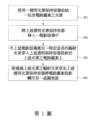
S11:使用一透明光罩保持容器收納一包含一電路圖案之光罩 S11: Use a transparent photomask holding container to accommodate a photomask containing a circuit pattern
S12:將上述透明光罩保持容器移入一微影設備中 S12: Move the above-mentioned transparent photomask holding container into a lithography device
S13:令上述微影設備產生一特定波長的輻射光束穿入上述透明光罩保持容器投射於上述光罩之電路圖案上 S13: Make the above-mentioned lithography equipment generate a radiation beam of a specific wavelength to penetrate the above-mentioned transparent photomask holding container and project on the circuit pattern of the above-mentioned photomask
S14:使通過上述光罩的輻射光束穿出上述透明光罩保持容器將電路圖案投影轉印至一晶圓的表面 S14: Let the radiation beam passing through the above-mentioned photomask pass through the above-mentioned transparent photomask holding container to project and transfer the circuit pattern to the surface of a wafer
S141:使射向上述光罩的輻射光束反射穿出上述透明光罩保持容器將電路圖案投影轉印至一晶圓的表面 S141: Reflecting the radiation beam directed at the above-mentioned mask through the above-mentioned transparent mask holding container to project and transfer the circuit pattern to the surface of a wafer
10:透明光罩保持容器 10: Transparent mask holding container
11:第一透明板面 11: The first transparent board
12:第二透明板面 12: The second transparent surface
15:基座 15: base
16:蓋體 16: cover body
100:光罩 100: mask
105:電路圖案 105: circuit pattern
200:晶圓 200: Wafer
50:微影設備 50: Lithography equipment
51:微影光束 51: Lithography Beam
第1圖:為本發明之微影方法的流程示意圖。 Figure 1: is a schematic flow chart of the lithography method of the present invention.
第2圖:為本發明之微影方法於實際使用時的架構示意圖。 Figure 2: It is a schematic diagram of the structure of the lithography method of the present invention in actual use.
第3圖:為本發明之微影方法中使用的光罩保持容器較佳實施例之外觀示意圖。 Figure 3: It is a schematic view of the appearance of a preferred embodiment of the photomask holding container used in the lithography method of the present invention.
第4圖:為本發明之微影方法中使用的光罩保持容器較佳實施例之分解外觀示意圖。 Fig. 4: It is an exploded appearance diagram of a preferred embodiment of the photomask holding container used in the lithography method of the present invention.
第5圖:為本發明之微影方法中使用的光罩保持容器較佳實施例於蓋合時的俯視平面示意圖。 Fig. 5: It is a top plan view of a preferred embodiment of the photomask holding container used in the lithography method of the present invention when it is closed.
第6圖:為本發明之微影方法另一實施例的流程示意圖。 Fig. 6: is a schematic flow chart of another embodiment of the lithography method of the present invention.
本發明係一種微影方法,隨附圖例示之本發明光罩保持容器的具體實施例及其構件中,所有關於前與後、左與右、頂部與底部、上部與下部、以及水平與垂直的參考,僅用於方便進行描述,並非限制本發明,亦非將其構件限制於任何位置或空間方向。圖式與說明書中所指定的尺寸,當可在不離 開本發明之申請專利範圍內,根據本發明之具體實施例的設計與需求而進行變化,故在專利申請上並不受此種結構之限制。 The present invention is a lithography method. In the specific embodiment of the photomask holding container of the present invention and its components illustrated in the accompanying drawings, all about front and back, left and right, top and bottom, upper and lower, and horizontal and vertical The references are for convenience of description only, and do not limit the present invention, nor limit its components to any position or spatial orientation. Dimensions specified in the drawings and instructions, when available without separation Within the scope of the patent application of the present invention, changes are made according to the design and requirements of the specific embodiments of the present invention, so the patent application is not limited by this structure.
有關本發明一種微影方法,請參照第1圖所示,其包含有使用一透明光罩保持容器收納一包含一電路圖案之光罩(S11)、將上述透明光罩保持容器移入一微影設備中(S12)、令上述微影設備產生一特定波長的輻射光束穿入上述透明光罩保持容器投射於上述光罩之電路圖案上(S13);以及使通過上述光罩的輻射光束穿出上述透明光罩保持容器將電路圖案投影轉印至一晶圓的表面(S14)。而完成光罩之電路圖案轉印至晶圓表面的微影製程; For a lithography method of the present invention, please refer to FIG. 1, which includes using a transparent photomask holding container to store a photomask containing a circuit pattern (S11), moving the above-mentioned transparent photomask holding container into a lithography In the equipment (S12), make the above-mentioned lithography equipment generate a radiation beam of a specific wavelength to penetrate the above-mentioned transparent photomask holding container and project on the circuit pattern of the above-mentioned photomask (S13); and make the radiation beam passing through the above-mentioned photomask pass out The above-mentioned transparent photomask holding container transfers the projection of the circuit pattern to the surface of a wafer ( S14 ). And complete the lithography process of transferring the circuit pattern of the mask to the surface of the wafer;
至於本發明之詳細架構說明,則係如第1、2圖所揭示者,其中: As for the detailed structure description of the present invention, it is as disclosed in Fig. 1 and Fig. 2, wherein:
步驟(S11)、使用一透明光罩保持容器收納一包含一電路圖案之光罩:其係將一光罩(100)收納限制於一透明光罩保持容器(10)內,如第3、4及5圖所示,其中該光罩(100)具有兩相對平行之表面,且該光罩(100)兩側表面中任一表面具有一供投影轉印之電路圖案(105)。根據某些實施例,該光罩(100)於具電路圖案(105)之表面覆設有一供保護該電路圖案(105)的透光薄膜〔110〕。另根據某些實施例,該光罩(100)具電路圖案(105)之表面塗覆有一反射層〔圖中未示〕,而該電路圖案(105)係形成於該反射層的表面,以利用反射技術轉印電路圖案(105)。而該透明光罩保持容器(10)可選擇性收納該光罩(100),又該透明光罩保持容器(10)具有對應該光罩(100)兩側表面之一第一透明板面(11)及一第二透明板面(12),且該第一、二透明板面(11、12)之透光率可大於或等於90%,又該第一、二透明板 面(11、12)之透光範圍大於或等於該光罩(100)之電路圖案(105)範圍,而根據某些實施例,該第一、二透明板面(11、12)可以選自純度大於或等於99.995%之石英玻璃,令其從紫外線、可見光到紅外波段都有良好的穿透率。再者,根據某些實施例,該透明光罩保持容器(10)是由可相對蓋合之一基座(15)及一蓋體(16)所構成,而該第一、二透明板面(11、12)係以平行方式分設於該基座(15)與該蓋體(16)之相對位置,且該基座(15)與該蓋體(16)除了該第一、二透明板面(11、12)外的材質可選自金屬或塑膠; Step (S11), using a transparent photomask holding container to store a photomask containing a circuit pattern: it is to store a photomask (100) within a transparent photomask holding container (10), as in the 3rd and 4th As shown in FIG. 5 , the photomask (100) has two relatively parallel surfaces, and any surface on both sides of the photomask (100) has a circuit pattern (105) for projection transfer. According to some embodiments, a light-transmitting film (110) for protecting the circuit pattern (105) is covered on the surface of the photomask (100) with the circuit pattern (105). Also according to some embodiments, the surface of the photomask (100) with the circuit pattern (105) is coated with a reflective layer (not shown in the figure), and the circuit pattern (105) is formed on the surface of the reflective layer, so as to The circuit pattern (105) is transferred using reflective technology. And this transparent photomask holding container (10) can selectively accommodate this photomask (100), and this transparent photomask holding container (10) has one of the first transparent plate surface corresponding to this photomask (100) both sides surfaces ( 11) and a second transparent plate surface (12), and the light transmittance of the first and second transparent plate surfaces (11, 12) can be greater than or equal to 90%, and the first and second transparent plate surfaces The light transmission range of the surface (11, 12) is greater than or equal to the range of the circuit pattern (105) of the photomask (100), and according to some embodiments, the first and second transparent plate surfaces (11, 12) can be selected from Quartz glass with a purity greater than or equal to 99.995% makes it have good transmittance from ultraviolet, visible light to infrared bands. Moreover, according to some embodiments, the transparent photomask holding container (10) is composed of a base (15) and a cover (16) that can be relatively closed, and the first and second transparent board surfaces (11, 12) are arranged in the relative positions of the base (15) and the cover (16) in a parallel manner, and the base (15) and the cover (16) except the first and second transparent The material outside the board surface (11, 12) can be selected from metal or plastic;
步驟(S12)、將上述透明光罩保持容器移入一微影設備中:接著將該收納有光罩(100)之透明光罩保持容器(10)載入一微影設備(50)中,該微影設備(50)可以是能生成特定波長之幅射光束的典型微影設備,如紫外光微影設備、深紫外光微影設備或極紫外光微影設備; Step (S12), moving the above-mentioned transparent photomask holding container into a lithography equipment: then loading the transparent photomask holding container (10) containing the photomask (100) into a lithography equipment (50), the The lithography device (50) may be a typical lithography device capable of generating a radiation beam of a specific wavelength, such as an ultraviolet lithography device, a deep ultraviolet lithography device or an extreme ultraviolet lithography device;
步驟(S13)、令上述微影設備產生一特定波長的輻射光束穿入上述透明光罩保持容器投射於上述光罩之電路圖案上:當上述透明光罩保持容器(10)移入上述微影設備(50)內部之工作位置後,上述微影設備(50)可生產生一射向該光罩(100)之特定波長的輻射光束(51),該輻射光束(51)可穿經上述透明光罩保持容器(10)之第一透明板面(11),而進入該透明光罩保持容器(10)內部且投射於上述光罩(100)之電路圖案(105)上;以及 Step (S13), making the above-mentioned lithography equipment generate a radiation beam of a specific wavelength to penetrate the above-mentioned transparent photomask holding container and project on the circuit pattern of the above-mentioned photomask: when the above-mentioned transparent photomask holding container (10) is moved into the above-mentioned lithography equipment (50) After the internal working position, the above-mentioned lithography equipment (50) can produce a radiation beam (51) of a specific wavelength directed at the mask (100), and the radiation beam (51) can pass through the above-mentioned transparent light The first transparent plate surface (11) of the mask holding container (10) enters the interior of the transparent photomask holding container (10) and projects on the circuit pattern (105) of the photomask (100); and
步驟(S14)、使通過上述光罩的輻射光束穿出上述透明光罩保持容器將電路圖案投影轉印至一晶圓的表面:而上述之輻射光束(51)在通過該光罩(100)後,可由該透明光罩保持容器(10)中相對第一透明板面(11)之第二透明板 面(12)穿出,使上述之輻射光束(51)將光罩(100)之電路圖案(105)投影轉印於一晶圓(200)之表面,而於該晶圓(200)表面投影轉印出複數電路圖案(105),進而完成該晶圓(200)之微影製程。 Step (S14), making the radiation beam passing through the photomask pass through the transparent photomask holding container to project and transfer the circuit pattern to the surface of a wafer: and the radiation beam (51) passing through the photomask (100) Afterwards, the second transparent plate opposite to the first transparent plate surface (11) in the container (10) can be held by the transparent mask The surface (12) passes through, so that the above-mentioned radiation beam (51) projects and transfers the circuit pattern (105) of the mask (100) onto the surface of a wafer (200), and projects on the surface of the wafer (200) A plurality of circuit patterns (105) are transferred and printed, and then the lithography process of the wafer (200) is completed.
藉此,使得輻射光束(51)可由該光罩保持容器外部射入、且經該光罩(100)後射出,供進行半導體元件之微影製程。 Thereby, the radiation beam (51) can enter from the outside of the photomask holding container and exit through the photomask (100) for the lithography process of the semiconductor element.
而本發明之微影製程具有另一實施例,其係如第6圖所示,其包含有使用一透明光罩保持容器收納一包含一電路圖案之光罩(S11)、將上述透明光罩保持容器移入一微影設備中(S12)、令上述微影設備產生一特定波長的輻射光束穿入上述透明光罩保持容器投射於上述光罩之電路圖案上(S13),以及使射向上述光罩的輻射光束反射穿出上述透明光罩保持容器將電路圖案投影轉印至一晶圓的表面(S141)。其中步驟(S11)~步驟(S13)與前述流程方法相同; And the photolithography process of the present invention has another embodiment, and it is as shown in Fig. 6, and it comprises using a transparent photomask holding container to accommodate a photomask (S11) that contains a circuit pattern, above-mentioned transparent photomask The holding container is moved into a lithography equipment (S12), and the above-mentioned lithography equipment is made to generate a radiation beam of a specific wavelength to penetrate the above-mentioned transparent photomask holding container and project on the circuit pattern of the above-mentioned photomask (S13), and make the radiation beam directed at the above-mentioned photomask The radiation beam of the photomask is reflected out of the transparent photomask holding container to project and transfer the circuit pattern to the surface of a wafer ( S141 ). Wherein step (S11) ~ step (S13) are identical with aforementioned flow process method;
而其中步驟(S141)、使射向上述光罩的輻射光束反射穿出上述透明光罩保持容器將電路圖案投影轉印至一晶圓的表面:則該光罩(100)可以選自電路圖案(105)係形成於表面(101)具反射層者,如此當該上述之輻射光束(51)在投射該光罩(100)後,上述之輻射光束(51)可以反射由該透明光罩保持容器(10)之第一透明板面(11)再次穿出,使上述之輻射光束(51)將光罩(100)之電路圖案(105)投影轉印於一晶圓(200)之表面。 In the step (S141), the radiation beam directed at the above-mentioned photomask is reflected to pass through the above-mentioned transparent photomask holding container, and the circuit pattern is projected and transferred to the surface of a wafer: then the photomask (100) can be selected from the circuit pattern (105) is formed on the surface (101) with a reflective layer, so that when the above-mentioned radiation beam (51) is projected on the mask (100), the above-mentioned radiation beam (51) can be reflected and kept by the transparent mask The first transparent plate surface (11) of the container (10) passes through again, so that the above-mentioned radiation beam (51) projects and transfers the circuit pattern (105) of the photomask (100) onto the surface of a wafer (200).
經由上述之說明,本發明之微影方法利用該透明光罩保持容器(10)可以使微影設備(50)之特定波長的輻射光束(51)通過之特殊設計,使得光罩(100)收納於光罩保 持容器內時,該輻射光束(51)能投射通過光罩(100)將電路圖案(105)轉印至晶圓(200)的表面,讓光罩(100)在微影製程使用過程中提高對於光罩(100)的保護需求,避免在微影製程中光罩因製程材料、微粒或氣體游離分子在經積聚或化學變化,而不致於光罩表面附著或產生不同缺陷,進而延長光罩(100)回廠整修的間隔時間,以及減少光罩(100)清洗的次數,而延長光罩(100)之電路圖案壽命,可以大幅的提高其生產效率,從而減少同一佈局之光罩的備用量,可以進一步整體製程成本。 Through the above description, the lithography method of the present invention utilizes the special design of the transparent photomask holding container (10) to allow the radiation beam (51) of a specific wavelength of the lithography equipment (50) to pass through, so that the photomask (100) can be stored In mask protection When held in the container, the radiation beam (51) can be projected through the photomask (100) to transfer the circuit pattern (105) to the surface of the wafer (200), so that the photomask (100) can be improved during the lithography process. For the protection requirements of the photomask (100), avoid the accumulation or chemical changes of the photomask due to process materials, particles or gas free molecules during the lithography process, so as not to cause adhesion or different defects on the photomask surface, thereby prolonging the photomask (100) the interval time of returning to the factory for refurbishment, and reducing the number of cleanings of the photomask (100), prolonging the life of the circuit pattern of the photomask (100), can greatly improve its production efficiency, thereby reducing the preparation of photomasks of the same layout The dosage can further the overall process cost.
綜上所述,可以理解到本發明為一創意極佳之新型創作,除了有效解決習式者所面臨的問題,更大幅增進功效,且在相同的技術領域中未見相同或近似的產品創作或公開使用,同時具有功效的增進,故本發明已符合新型專利有關「新穎性」與「進步性」的要件,乃依法提出申請新型專利。 To sum up, it can be understood that the present invention is a new creation with excellent creativity. In addition to effectively solving the problems faced by the practitioners, it can greatly improve the efficacy, and there is no identical or similar product creation in the same technical field. Or open use, and at the same time have the enhancement of efficacy, so the present invention has met the requirements of "novelty" and "progressiveness" of a new patent, and an application for a new patent is filed according to law.
S11:使用一透明光罩保持容器收納一包含一電路圖案之光罩 S11: Use a transparent photomask holding container to accommodate a photomask containing a circuit pattern
S12:將上述透明光罩保持容器移入一微影設備中 S12: Move the above-mentioned transparent photomask holding container into a lithography device
S13:令上述微影設備產生一特定波長的輻射光束穿入上述透明光罩保持容器投射於上述光罩之電路圖案上 S13: Make the above-mentioned lithography equipment generate a radiation beam of a specific wavelength to penetrate the above-mentioned transparent photomask holding container and project on the circuit pattern of the above-mentioned photomask
S14:使通過上述光罩的輻射光束穿出上述透明光罩保持容器將電路圖案投影轉印至一晶圓的表面 S14: Let the radiation beam passing through the above-mentioned photomask pass through the above-mentioned transparent photomask holding container to project and transfer the circuit pattern to the surface of a wafer
Claims (7)
Priority Applications (4)
| Application Number | Priority Date | Filing Date | Title |
|---|---|---|---|
| TW110145912A TWI896820B (en) | 2021-12-08 | 2021-12-08 | Lithography |
| US17/858,075 US20230176472A1 (en) | 2021-12-08 | 2022-07-06 | Lithographic method by using a photomask contained in a transparent pod |
| KR1020220168662A KR20230086605A (en) | 2021-12-08 | 2022-12-06 | Lithographic method by using a photomask contained in a transparent pod |
| NL2033682A NL2033682B1 (en) | 2021-12-08 | 2022-12-07 | Lithographic method by using a photomask contained in a transparent pod |
Applications Claiming Priority (1)
| Application Number | Priority Date | Filing Date | Title |
|---|---|---|---|
| TW110145912A TWI896820B (en) | 2021-12-08 | 2021-12-08 | Lithography |
Publications (2)
| Publication Number | Publication Date |
|---|---|
| TW202324495A true TW202324495A (en) | 2023-06-16 |
| TWI896820B TWI896820B (en) | 2025-09-11 |
Family
ID=86604733
Family Applications (1)
| Application Number | Title | Priority Date | Filing Date |
|---|---|---|---|
| TW110145912A TWI896820B (en) | 2021-12-08 | 2021-12-08 | Lithography |
Country Status (4)
| Country | Link |
|---|---|
| US (1) | US20230176472A1 (en) |
| KR (1) | KR20230086605A (en) |
| NL (1) | NL2033682B1 (en) |
| TW (1) | TWI896820B (en) |
Families Citing this family (1)
| Publication number | Priority date | Publication date | Assignee | Title |
|---|---|---|---|---|
| US20240092545A1 (en) * | 2022-09-21 | 2024-03-21 | Tae Technologies, Inc. | Systems, devices, and methods for transport and storage of air-sensitive materials |
Family Cites Families (17)
| Publication number | Priority date | Publication date | Assignee | Title |
|---|---|---|---|---|
| JPS59208715A (en) * | 1983-05-13 | 1984-11-27 | Hitachi Ltd | Mask protection apparatus |
| JPS59208716A (en) * | 1983-05-13 | 1984-11-27 | Hitachi Ltd | Mask protection apparatus |
| JPH04140753A (en) * | 1990-10-02 | 1992-05-14 | Fujitsu Ltd | Exposure device and exposure method |
| JPH1116802A (en) * | 1997-06-19 | 1999-01-22 | Toshiba Corp | Exposure method and exposure apparatus |
| US20020089656A1 (en) * | 2001-01-09 | 2002-07-11 | Cheng Guo | Containers for lithography mask and method of use |
| EP1434094A1 (en) * | 2002-12-27 | 2004-06-30 | ASML Netherlands B.V. | Container for a mask |
| US11914287B2 (en) * | 2017-07-21 | 2024-02-27 | Entegris, Inc. | Container for holding and transporting reticles having a transparent window assembly |
| US11131929B2 (en) * | 2018-11-07 | 2021-09-28 | Waymo Llc | Systems and methods that utilize angled photolithography for manufacturing light guide elements |
| KR102729017B1 (en) * | 2019-10-10 | 2024-11-14 | 엔테그리스, 아이엔씨. | Reticle pod with window |
| US11314164B2 (en) * | 2019-12-31 | 2022-04-26 | Taiwan Semiconductor Manufacturing Company Ltd. | Structure and method of reticle pod having inspection window |
| CN111913346A (en) * | 2020-08-25 | 2020-11-10 | 泉芯集成电路制造(济南)有限公司 | Photomask assembly and photoetching system |
| TWM633261U (en) * | 2021-12-08 | 2022-10-21 | 陳啓仲 | Photomask supporting container for lithography-based application |
| TWI868412B (en) * | 2021-12-08 | 2025-01-01 | 陳啓仲 | Photomask detection method and transparent photomask holding container |
| US20230176473A1 (en) * | 2021-12-08 | 2023-06-08 | Chi-Chung Chen | Pod for containing a photomask |
| US20230393489A1 (en) * | 2022-06-01 | 2023-12-07 | Taiwan Semiconductor Manufacturing Company, Ltd. | Detection method of euv pellicle status |
| CN117470866A (en) * | 2022-07-21 | 2024-01-30 | 特铨股份有限公司 | Stage mechanism used in photomask inspection machines |
| CN117470873A (en) * | 2022-07-21 | 2024-01-30 | 特铨股份有限公司 | Mask surface inspection device |
-
2021
- 2021-12-08 TW TW110145912A patent/TWI896820B/en active
-
2022
- 2022-07-06 US US17/858,075 patent/US20230176472A1/en not_active Abandoned
- 2022-12-06 KR KR1020220168662A patent/KR20230086605A/en not_active Ceased
- 2022-12-07 NL NL2033682A patent/NL2033682B1/en active
Also Published As
| Publication number | Publication date |
|---|---|
| NL2033682B1 (en) | 2024-01-04 |
| NL2033682A (en) | 2023-06-22 |
| TWI896820B (en) | 2025-09-11 |
| US20230176472A1 (en) | 2023-06-08 |
| KR20230086605A (en) | 2023-06-15 |
Similar Documents
| Publication | Publication Date | Title |
|---|---|---|
| US20230367194A1 (en) | Extreme ultraviolet mask with reduced wafer neighboring effect | |
| TW562965B (en) | System and method for reticle protection and transport | |
| US20220260901A1 (en) | Method of lithography process using reticle container with discharging device | |
| TWI761607B (en) | Pellicle frame, pellicle assembly, ventilation structure, exposure master, exposure method, semiconductor device manufacturing method, and liquid crystal display manufacturing method | |
| US20020179852A1 (en) | Apparatus and method for removing photomask contamination and controlling electrostatic discharge | |
| KR20210048152A (en) | Manufacturing method for a Pellicle including integrated frame and membrane | |
| US11762282B2 (en) | Pellicle design for mask | |
| TWM633261U (en) | Photomask supporting container for lithography-based application | |
| TW202324495A (en) | Lithography method | |
| TWI868412B (en) | Photomask detection method and transparent photomask holding container | |
| US8888086B2 (en) | Apparatus with surface protector to inhibit contamination | |
| JP4396354B2 (en) | Photo mask | |
| CN217279258U (en) | Reticle holding container for lithography | |
| TWI270504B (en) | Photo-mask protection film frame | |
| CN110955111B (en) | Photomask and photolithography method using the same | |
| CN116300296A (en) | Lithographic method | |
| CN113050361B (en) | Method for manufacturing semiconductor element | |
| US6569582B2 (en) | Hinged pellicles and methods of use | |
| JP2004061884A (en) | Photomask | |
| TW202323984A (en) | Reticle holding container based on lithography application | |
| US20210132515A1 (en) | Extreme ultraviolet exposure system | |
| US8268541B2 (en) | Mask and blank storage inner gas | |
| CN116300305A (en) | Reticle holding container for lithography-based applications | |
| JP2013243354A (en) | Semiconductor circuit exposure method and exposure device | |
| US20120200921A1 (en) | Pellicle frame |