TW201803409A - Laminated reflective electrode film, laminated reflective electrode pattern, and laminated reflective electrode pattern manufacturing method - Google Patents
Laminated reflective electrode film, laminated reflective electrode pattern, and laminated reflective electrode pattern manufacturing method Download PDFInfo
- Publication number
- TW201803409A TW201803409A TW106109573A TW106109573A TW201803409A TW 201803409 A TW201803409 A TW 201803409A TW 106109573 A TW106109573 A TW 106109573A TW 106109573 A TW106109573 A TW 106109573A TW 201803409 A TW201803409 A TW 201803409A
- Authority
- TW
- Taiwan
- Prior art keywords
- film
- reflective electrode
- laminated reflective
- transparent conductive
- conductive oxide
- Prior art date
Links
- 238000004519 manufacturing process Methods 0.000 title claims description 22
- 229910052719 titanium Inorganic materials 0.000 claims abstract description 44
- 229910052727 yttrium Inorganic materials 0.000 claims abstract description 44
- 229910001316 Ag alloy Inorganic materials 0.000 claims abstract description 24
- 229910052725 zinc Inorganic materials 0.000 claims abstract description 17
- 229910052733 gallium Inorganic materials 0.000 claims abstract description 11
- 229910001887 tin oxide Inorganic materials 0.000 claims abstract description 3
- 238000005530 etching Methods 0.000 claims description 49
- 229910052718 tin Inorganic materials 0.000 claims description 42
- 239000000758 substrate Substances 0.000 claims description 41
- QTBSBXVTEAMEQO-UHFFFAOYSA-N Acetic acid Chemical compound CC(O)=O QTBSBXVTEAMEQO-UHFFFAOYSA-N 0.000 claims description 33
- 238000000034 method Methods 0.000 claims description 26
- NBIIXXVUZAFLBC-UHFFFAOYSA-N Phosphoric acid Chemical compound OP(O)(O)=O NBIIXXVUZAFLBC-UHFFFAOYSA-N 0.000 claims description 20
- 229910052751 metal Inorganic materials 0.000 claims description 18
- 239000002184 metal Substances 0.000 claims description 15
- 229910052737 gold Inorganic materials 0.000 claims description 14
- 229910052693 Europium Inorganic materials 0.000 claims description 13
- 229910052688 Gadolinium Inorganic materials 0.000 claims description 13
- 229910052779 Neodymium Inorganic materials 0.000 claims description 13
- 229910052772 Samarium Inorganic materials 0.000 claims description 13
- 229910052771 Terbium Inorganic materials 0.000 claims description 13
- 229910052787 antimony Inorganic materials 0.000 claims description 13
- 239000007788 liquid Substances 0.000 claims description 13
- 229910052749 magnesium Inorganic materials 0.000 claims description 13
- 229910052697 platinum Inorganic materials 0.000 claims description 13
- 229910052706 scandium Inorganic materials 0.000 claims description 13
- 229910052691 Erbium Inorganic materials 0.000 claims description 12
- 229910000147 aluminium phosphate Inorganic materials 0.000 claims description 10
- 239000011259 mixed solution Substances 0.000 claims description 10
- 230000002378 acidificating effect Effects 0.000 claims description 7
- 239000012535 impurity Substances 0.000 claims description 5
- 239000010408 film Substances 0.000 description 361
- 238000005401 electroluminescence Methods 0.000 description 31
- 239000011701 zinc Substances 0.000 description 21
- 239000002585 base Substances 0.000 description 18
- 230000015572 biosynthetic process Effects 0.000 description 17
- 238000004544 sputter deposition Methods 0.000 description 14
- XLOMVQKBTHCTTD-UHFFFAOYSA-N Zinc monoxide Chemical compound [Zn]=O XLOMVQKBTHCTTD-UHFFFAOYSA-N 0.000 description 13
- 239000003513 alkali Substances 0.000 description 13
- 239000010931 gold Substances 0.000 description 13
- 229910052802 copper Inorganic materials 0.000 description 12
- 230000006866 deterioration Effects 0.000 description 12
- 229910052738 indium Inorganic materials 0.000 description 12
- 239000000203 mixture Substances 0.000 description 10
- 230000000052 comparative effect Effects 0.000 description 8
- 230000000694 effects Effects 0.000 description 8
- 238000012360 testing method Methods 0.000 description 8
- 229910052760 oxygen Inorganic materials 0.000 description 7
- 206010040844 Skin exfoliation Diseases 0.000 description 6
- 239000007789 gas Substances 0.000 description 6
- 239000000243 solution Substances 0.000 description 6
- 239000011787 zinc oxide Substances 0.000 description 6
- 239000001301 oxygen Substances 0.000 description 5
- 238000000059 patterning Methods 0.000 description 5
- 229910052709 silver Inorganic materials 0.000 description 5
- 230000007613 environmental effect Effects 0.000 description 4
- 238000002834 transmittance Methods 0.000 description 4
- NINIDFKCEFEMDL-UHFFFAOYSA-N Sulfur Chemical compound [S] NINIDFKCEFEMDL-UHFFFAOYSA-N 0.000 description 3
- 229910052782 aluminium Inorganic materials 0.000 description 3
- 229910052732 germanium Inorganic materials 0.000 description 3
- 239000011521 glass Substances 0.000 description 3
- 238000010030 laminating Methods 0.000 description 3
- 238000005259 measurement Methods 0.000 description 3
- 229910044991 metal oxide Inorganic materials 0.000 description 3
- 150000004706 metal oxides Chemical class 0.000 description 3
- 238000012986 modification Methods 0.000 description 3
- 230000004048 modification Effects 0.000 description 3
- -1 oxygen ions Chemical class 0.000 description 3
- 229910052763 palladium Inorganic materials 0.000 description 3
- 239000000523 sample Substances 0.000 description 3
- 238000005486 sulfidation Methods 0.000 description 3
- 229910052717 sulfur Inorganic materials 0.000 description 3
- 239000011593 sulfur Substances 0.000 description 3
- QVGXLLKOCUKJST-UHFFFAOYSA-N atomic oxygen Chemical compound [O] QVGXLLKOCUKJST-UHFFFAOYSA-N 0.000 description 2
- 230000003287 optical effect Effects 0.000 description 2
- 238000000206 photolithography Methods 0.000 description 2
- 239000004332 silver Substances 0.000 description 2
- GYHNNYVSQQEPJS-UHFFFAOYSA-N Gallium Chemical compound [Ga] GYHNNYVSQQEPJS-UHFFFAOYSA-N 0.000 description 1
- GRYLNZFGIOXLOG-UHFFFAOYSA-N Nitric acid Chemical compound O[N+]([O-])=O GRYLNZFGIOXLOG-UHFFFAOYSA-N 0.000 description 1
- OAICVXFJPJFONN-UHFFFAOYSA-N Phosphorus Chemical compound [P] OAICVXFJPJFONN-UHFFFAOYSA-N 0.000 description 1
- 238000010521 absorption reaction Methods 0.000 description 1
- 239000002253 acid Substances 0.000 description 1
- 239000000654 additive Substances 0.000 description 1
- 230000000996 additive effect Effects 0.000 description 1
- 230000004520 agglutination Effects 0.000 description 1
- 238000000149 argon plasma sintering Methods 0.000 description 1
- 238000003339 best practice Methods 0.000 description 1
- 229910052797 bismuth Inorganic materials 0.000 description 1
- 230000015556 catabolic process Effects 0.000 description 1
- 150000001875 compounds Chemical class 0.000 description 1
- 238000012790 confirmation Methods 0.000 description 1
- 238000006731 degradation reaction Methods 0.000 description 1
- 238000011161 development Methods 0.000 description 1
- 239000012776 electronic material Substances 0.000 description 1
- 238000005516 engineering process Methods 0.000 description 1
- 238000011156 evaluation Methods 0.000 description 1
- 238000002474 experimental method Methods 0.000 description 1
- 239000000284 extract Substances 0.000 description 1
- PCHJSUWPFVWCPO-UHFFFAOYSA-N gold Chemical compound [Au] PCHJSUWPFVWCPO-UHFFFAOYSA-N 0.000 description 1
- 239000008187 granular material Substances 0.000 description 1
- 238000010438 heat treatment Methods 0.000 description 1
- 230000001678 irradiating effect Effects 0.000 description 1
- 229910052748 manganese Inorganic materials 0.000 description 1
- 229910017604 nitric acid Inorganic materials 0.000 description 1
- TWNQGVIAIRXVLR-UHFFFAOYSA-N oxo(oxoalumanyloxy)alumane Chemical compound O=[Al]O[Al]=O TWNQGVIAIRXVLR-UHFFFAOYSA-N 0.000 description 1
- 229910052698 phosphorus Inorganic materials 0.000 description 1
- 239000011574 phosphorus Substances 0.000 description 1
- 238000009832 plasma treatment Methods 0.000 description 1
- 238000004445 quantitative analysis Methods 0.000 description 1
- 238000000985 reflectance spectrum Methods 0.000 description 1
- 238000002310 reflectometry Methods 0.000 description 1
- 239000011347 resin Substances 0.000 description 1
- 229920005989 resin Polymers 0.000 description 1
- 238000005987 sulfurization reaction Methods 0.000 description 1
- 239000010409 thin film Substances 0.000 description 1
Classifications
-
- H—ELECTRICITY
- H01—ELECTRIC ELEMENTS
- H01B—CABLES; CONDUCTORS; INSULATORS; SELECTION OF MATERIALS FOR THEIR CONDUCTIVE, INSULATING OR DIELECTRIC PROPERTIES
- H01B1/00—Conductors or conductive bodies characterised by the conductive materials; Selection of materials as conductors
- H01B1/02—Conductors or conductive bodies characterised by the conductive materials; Selection of materials as conductors mainly consisting of metals or alloys
-
- H—ELECTRICITY
- H05—ELECTRIC TECHNIQUES NOT OTHERWISE PROVIDED FOR
- H05B—ELECTRIC HEATING; ELECTRIC LIGHT SOURCES NOT OTHERWISE PROVIDED FOR; CIRCUIT ARRANGEMENTS FOR ELECTRIC LIGHT SOURCES, IN GENERAL
- H05B33/00—Electroluminescent light sources
- H05B33/10—Apparatus or processes specially adapted to the manufacture of electroluminescent light sources
-
- H—ELECTRICITY
- H05—ELECTRIC TECHNIQUES NOT OTHERWISE PROVIDED FOR
- H05B—ELECTRIC HEATING; ELECTRIC LIGHT SOURCES NOT OTHERWISE PROVIDED FOR; CIRCUIT ARRANGEMENTS FOR ELECTRIC LIGHT SOURCES, IN GENERAL
- H05B33/00—Electroluminescent light sources
- H05B33/12—Light sources with substantially two-dimensional radiating surfaces
- H05B33/26—Light sources with substantially two-dimensional radiating surfaces characterised by the composition or arrangement of the conductive material used as an electrode
-
- H—ELECTRICITY
- H10—SEMICONDUCTOR DEVICES; ELECTRIC SOLID-STATE DEVICES NOT OTHERWISE PROVIDED FOR
- H10K—ORGANIC ELECTRIC SOLID-STATE DEVICES
- H10K50/00—Organic light-emitting devices
-
- H—ELECTRICITY
- H10—SEMICONDUCTOR DEVICES; ELECTRIC SOLID-STATE DEVICES NOT OTHERWISE PROVIDED FOR
- H10K—ORGANIC ELECTRIC SOLID-STATE DEVICES
- H10K50/00—Organic light-emitting devices
- H10K50/80—Constructional details
- H10K50/805—Electrodes
- H10K50/81—Anodes
- H10K50/818—Reflective anodes, e.g. ITO combined with thick metallic layers
-
- H—ELECTRICITY
- H10—SEMICONDUCTOR DEVICES; ELECTRIC SOLID-STATE DEVICES NOT OTHERWISE PROVIDED FOR
- H10K—ORGANIC ELECTRIC SOLID-STATE DEVICES
- H10K59/00—Integrated devices, or assemblies of multiple devices, comprising at least one organic light-emitting element covered by group H10K50/00
- H10K59/80—Constructional details
- H10K59/805—Electrodes
- H10K59/8051—Anodes
- H10K59/80518—Reflective anodes, e.g. ITO combined with thick metallic layers
-
- H—ELECTRICITY
- H10—SEMICONDUCTOR DEVICES; ELECTRIC SOLID-STATE DEVICES NOT OTHERWISE PROVIDED FOR
- H10K—ORGANIC ELECTRIC SOLID-STATE DEVICES
- H10K71/00—Manufacture or treatment specially adapted for the organic devices covered by this subclass
-
- H—ELECTRICITY
- H10—SEMICONDUCTOR DEVICES; ELECTRIC SOLID-STATE DEVICES NOT OTHERWISE PROVIDED FOR
- H10K—ORGANIC ELECTRIC SOLID-STATE DEVICES
- H10K71/00—Manufacture or treatment specially adapted for the organic devices covered by this subclass
- H10K71/60—Forming conductive regions or layers, e.g. electrodes
-
- H—ELECTRICITY
- H10—SEMICONDUCTOR DEVICES; ELECTRIC SOLID-STATE DEVICES NOT OTHERWISE PROVIDED FOR
- H10K—ORGANIC ELECTRIC SOLID-STATE DEVICES
- H10K2102/00—Constructional details relating to the organic devices covered by this subclass
Landscapes
- Engineering & Computer Science (AREA)
- Manufacturing & Machinery (AREA)
- Physics & Mathematics (AREA)
- Optics & Photonics (AREA)
- Electroluminescent Light Sources (AREA)
- Laminated Bodies (AREA)
Abstract
本發明之層合反射電極膜,其係具有由Ag或Ag合金所成之Ag膜、與配置於前述Ag膜上之透明導電氧化物膜,前述透明導電氧化物膜係由包含Zn與Ga、進而包含Sn、Y及Ti中之1種或2種以上之氧化物所成。 The laminated reflective electrode film of the present invention comprises an Ag film made of Ag or an Ag alloy and a transparent conductive oxide film disposed on the Ag film, wherein the transparent conductive oxide film contains Zn and Ga, Further, it is composed of one or two or more oxides of Sn, Y and Ti.
Description
本發明為關於可使用作為例如有機電致發光(EL)元件之陽極的層合反射電極膜、由該層合反射電極膜所成之層合反射電極圖型及層合反射電極圖型之製造方法。 The present invention relates to a laminate reflective electrode film which can be used as an anode of, for example, an organic electroluminescence (EL) element, a laminated reflective electrode pattern formed by the laminated reflective electrode film, and a laminated reflective electrode pattern. method.
本申請案係基於2016年3月23日在日本申請的特願2016-059097號、及2017年2月13日在日本申請的特願2017-024269號主張優先權,在此引用其內容。 The present application claims priority based on Japanese Patent Application No. 2016-059097, filed on Jan.
一般而言,有機EL顯示器係由排列在透明基板上的有機EL元件所成。有機EL元件係由在透明基板上形成為指定圖型的陽極、有機EL發光層、與陰極所成,並將來自陽極之電洞、來自陰極之電子分別注入於有機EL膜中,利用在有機EL發光層之電洞與電子結合之 際所發出之光之原理而成的發光元件。 In general, an organic EL display is formed of an organic EL element arranged on a transparent substrate. The organic EL device is formed of an anode, an organic EL light-emitting layer, and a cathode formed on a transparent substrate, and a hole from the anode and an electron from the cathode are injected into the organic EL film, respectively. The hole of the EL luminescent layer is combined with electrons A light-emitting element made up of the principle of light emitted by the room.
作為有機EL元件之光取出之方式,已知有將光從透明基板側取出之「底部發射方式」、與將光從與透明基板為相反側取出之「頂部發射方式」。於此,相較於底部發射方式,由於頂部發射方式之開口率高,故有利於高輝度化。在頂部發射方式的有機EL元件中使用的陽極,為了能效率良好地將電致發光層產生的光取出至外部,期望著具有:高反射率、高導電率、可效率良好地將電洞注入至電致發光層般的高工作函數(work function)。 As a method of extracting light from the organic EL element, a "bottom emission method" for taking out light from the transparent substrate side and a "top emission method" for taking out light from the side opposite to the transparent substrate are known. Herein, compared with the bottom emission mode, since the aperture ratio of the top emission mode is high, it is advantageous for high luminance. In order to efficiently extract the light generated by the electroluminescent layer to the outside, the anode used in the top emission type organic EL element is desired to have a high reflectance and a high conductivity and efficiently inject a hole. A high work function like an electroluminescent layer.
例如在專利文獻1、2中作為有機EL元件之陽極,係使用對於金屬膜之表面施予氧等離子處理等形成表面氧化膜,以增加工作函數而成的層合膜。 For example, in Patent Documents 1 and 2, as the anode of the organic EL element, a laminated film obtained by applying a surface oxide film or the like to the surface of the metal film to increase the work function is used.
又,進而在專利文獻3、4、5中作為有機EL元件之電極,係使用在金屬膜之表面形成ITO膜等的透明導電膜而成的層合膜。更,在專利文獻6中作為有機EL元件之陽極,係使用對於ITO膜之表面照射氧離子或電子來施予表面改質,以增加工作函數而成的表面改質ITO膜。 Furthermore, in the electrodes of the organic EL element, a laminated film in which a transparent conductive film such as an ITO film is formed on the surface of the metal film is used in the patent documents 3, 4, and 5. Further, in Patent Document 6, as the anode of the organic EL element, a surface-modified ITO film obtained by irradiating oxygen ions or electrons to the surface of the ITO film to impart surface modification to increase the work function is used.
專利文獻7中記載,在以Ag作為主成分的導電層上層合金屬氧化物薄膜而成的層合膜,其中作為金屬氧化物為使用氧化鋅(ZnO)、添加鋁的氧化鋅(AZO)、添加鎵的氧化鋅(GZO)。 Patent Document 7 discloses a laminated film obtained by laminating a metal oxide thin film on a conductive layer containing Ag as a main component, wherein zinc oxide (ZnO), aluminum-added zinc oxide (AZO), or aluminum oxide is used as the metal oxide. Add gallium zinc oxide (GZO).
但,如非專利文獻1中記載般,包含ZnO的金屬氧 化物,容易溶解在蝕刻法所使用的阻劑的剝離液(弱鹼)中。因此,將使用包含AZO或GZO等的ZnO的金屬氧化物而成的層合膜,藉由蝕刻法來形成可作為有機EL顯示器用之電極使用般的微細的電極圖型為困難的。 However, as described in Non-Patent Document 1, metal oxygen containing ZnO The compound is easily dissolved in a stripping solution (weak base) of a resist used in the etching method. Therefore, it is difficult to form a fine electrode pattern which can be used as an electrode for an organic EL display by an etching method using a laminated film containing a metal oxide of ZnO such as AZO or GZO.
〔專利文獻1〕日本特開2006-294261號公報 [Patent Document 1] Japanese Patent Laid-Open Publication No. 2006-294261
〔專利文獻2〕國際公開第2010/032443號 [Patent Document 2] International Publication No. 2010/032443
〔專利文獻3〕日本特開2006-98856號公報 [Patent Document 3] Japanese Patent Laid-Open Publication No. 2006-98856
〔專利文獻4〕日本特開2011-9790號公報 [Patent Document 4] Japanese Patent Laid-Open Publication No. 2011-9790
〔專利文獻5〕日本特開2004-103247號公報 [Patent Document 5] Japanese Patent Laid-Open Publication No. 2004-103247
〔專利文獻6〕日本特開2000-133466號公報 [Patent Document 6] Japanese Patent Laid-Open Publication No. 2000-133466
〔專利文獻7〕日本特開2012-246511號公報 [Patent Document 7] Japanese Patent Laid-Open Publication No. 2012-246511
〔非專利文獻1〕日本學術振興會透明氧化物光‧電子材料第166委員會編、「透明導電膜之技術(改訂2版)」、Ohmsha股份有限公司、平成18年12月20日改訂2版第1刷發行、P.171-172 [Non-Patent Document 1] The Japan Society for the Promotion of Science, Transparent Oxide Light, Electronic Materials, Section 166, "Transparent Conductive Film Technology (Revised 2)", Ohmsha Co., Ltd., December 20, 2008, revised 2nd edition The first brush release, P.171-172
近來有機EL元件等已進展至微細化及高輝度 化,對於上述層合反射電極膜係要求著:與純銀同等級的低電阻、及高反射率。又,在製造有機EL元件之際,必須是可容易藉由蝕刻法來形成由層合反射電極膜所成之微細電極圖型。 Recently, organic EL elements and the like have progressed to miniaturization and high luminance. For the above-mentioned laminated reflective electrode film, it is required to have the same low resistance and high reflectance as pure silver. Further, in the production of an organic EL device, it is necessary to form a fine electrode pattern formed by laminating a reflective electrode film by an etching method.
然而,專利文獻1、2中所記載的具有表面氧化膜的層合膜之中,由於氧等離子處理之際之損傷(damage),會有造成反射率降低之同時電阻率亦為上升之虞。又,若使用由純銀所成之Ag膜來作為金屬膜時,耐硫化性將變得不足,會有因為在大氣中之使用而造成反射率降低,同時電阻率亦為上升之虞。 However, among the laminated films having the surface oxide film described in Patent Documents 1 and 2, the damage at the time of oxygen plasma treatment causes a decrease in reflectance and an increase in resistivity. Further, when an Ag film made of pure silver is used as the metal film, the sulfurization resistance is insufficient, and the reflectance is lowered due to use in the atmosphere, and the electrical resistivity is also increased.
另一方面,專利文獻3、4、5中所記載的形成有ITO等的透明導電膜而成的層合膜之中,可見光的反射率,特別是藍色區域(400~500nm)的光的反射率有降低之虞。特以,如專利文獻6中記載般,當對於ITO膜之表面照射氧離子或電子來施予表面改質時,ITO膜之表面會被弄粗,而有光散射之虞。又,Ag合金膜與ITO膜之層合膜,在藉由蝕刻來形成電極圖型之際,相較於ITO膜,Ag合金膜之蝕刻速度為快,因此若使用相同的蝕刻液來進行一次性蝕刻(one-time etching)時,會有Ag合金膜被過度蝕刻、或產生ITO膜殘渣之虞。 On the other hand, in the laminated film in which the transparent conductive film of ITO or the like is formed in the patent documents 3, 4, and 5, the reflectance of visible light, especially the light of the blue region (400 to 500 nm) The reflectance is reduced. In particular, as described in Patent Document 6, when the surface of the ITO film is irradiated with oxygen ions or electrons to impart surface modification, the surface of the ITO film is roughened and light scattering is caused. Further, when the laminated film of the Ag alloy film and the ITO film is formed by etching to form an electrode pattern, the etching rate of the Ag alloy film is faster than that of the ITO film. Therefore, the same etching solution is used once. In the case of one-time etching, the Ag alloy film is excessively etched or the ITO film residue is generated.
本發明係有鑑於前述情事之發明,目的係以提供一種可見光區域(特別是藍色區域)的反射率高、電阻值低、且可容易藉由蝕刻法形成微細的電極圖型的層合反射電極膜,以及提供由該層合反射電極膜所成之層合反 射電極圖型及層合反射電極圖型之製造方法。 The present invention has been made in view of the foregoing circumstances, and an object thereof is to provide a laminated reflection having a high reflectance of a visible light region (particularly a blue region), a low resistance value, and an electrode pattern which can be easily formed by etching. An electrode film, and providing a laminate reversed by the laminated reflective electrode film A method of manufacturing an electrode pattern and a laminated reflection electrode pattern.
為了解決上述課題,本發明之層合反射電極膜,其特徵係具有由Ag或Ag合金所成之Ag膜、與配置於前述Ag膜上之透明導電氧化物膜,前述透明導電氧化物膜係由包含Zn與Ga、進而包含Sn、Y及Ti中之1種或2種以上之氧化物所成。 In order to solve the above problems, the laminated reflective electrode film of the present invention is characterized in that it has an Ag film made of Ag or an Ag alloy and a transparent conductive oxide film disposed on the Ag film, and the transparent conductive oxide film is It is made of an oxide containing Zn and Ga and further containing one or more of Sn, Y, and Ti.
藉由本發明之層合反射電極膜,由於具有「Ag膜」,故電阻為低。然後,於該Ag膜上係配置「透明導電氧化物膜」,該透明導電氧化物膜係由包含Zn與Ga、進而包含Sn、Y及Ti中之1種或2種以上之氧化物所成,故可見光(特別是藍色區域)的光的反射率會變高。此係認為是由於,相較於ITO等的其他的透明導電氧化物,上述透明導電氧化物膜的可見光區域(特別是藍色區域)的折射率為低所致。 According to the laminated reflective electrode film of the present invention, since the "Ag film" is provided, the electric resistance is low. Then, a "transparent conductive oxide film" is formed on the Ag film, and the transparent conductive oxide film is made of ZnO and Ga, and further contains one or more oxides of Sn, Y, and Ti. Therefore, the reflectance of light in visible light (especially in the blue region) becomes high. This is considered to be because the refractive index of the visible light region (particularly the blue region) of the transparent conductive oxide film is low compared to other transparent conductive oxides such as ITO.
又,上述透明導電氧化物膜係包含Sn、Y及Ti中之1種或2種以上,因此耐鹼性會提升,而難以溶解於鹼性的阻劑除去液之中。因此,本發明之層合反射電極膜可藉由蝕刻法來形成電極圖型。 In addition, since the transparent conductive oxide film contains one or more of Sn, Y, and Ti, the alkali resistance is increased, and it is difficult to dissolve in the alkaline resist removal liquid. Therefore, the laminated reflective electrode film of the present invention can be formed into an electrode pattern by an etching method.
更,在藉由蝕刻法來形成電極圖型之際,若對於上述Ag膜與透明導電氧化物膜使用包含磷酸、乙酸的酸性混合液時,蝕刻速度之差將會變小。因此,本發明之層合反射電極膜在藉由蝕刻法形成電極圖型之際,將可減少過度 蝕刻之產生量。 Further, when an electrode pattern is formed by an etching method, when an acidic mixed solution containing phosphoric acid or acetic acid is used for the Ag film and the transparent conductive oxide film, the difference in etching rate is small. Therefore, the laminated reflective electrode film of the present invention can reduce excessiveity when forming an electrode pattern by etching The amount of etching produced.
尚,由於上述透明導電氧化物膜之工作函數較ITO為高,故即使是未進行藉由氧離子或電子之照射的表面改質,亦能使用上述透明導電氧化物膜。 Further, since the operation function of the transparent conductive oxide film is higher than that of ITO, the transparent conductive oxide film can be used even if surface modification by irradiation with oxygen ions or electrons is not performed.
於此,本發明之層合反射電極膜之中,前述透明導電氧化物膜中所包含之全金屬元素的原子比例,較佳為:Ga係0.5原子%以上30.0原子%以下,Sn、Y及Ti係分別為0.1原子%以上10.0原子%以下,其餘為Zn。 In the laminated reflective electrode film of the present invention, the atomic ratio of the total metal element contained in the transparent conductive oxide film is preferably 0.5 atom% or more and 30.0 atom% or less of the Ga system, and Sn, Y and Ti is 0.1 atom% or more and 10.0 atom% or less, and the rest is Zn.
此情形時,透明導電氧化物膜中所包含之全金屬元素中,由於Ga的含量係設為0.5原子%以上30.0原子%以下之範圍內,故可抑制電阻之增加,同時使Ag膜與透明導電氧化物膜之密著性提升。又,由於Sn、Y及Ti的合計量係分別設為0.1原子%以上10.0原子%以下之範圍內,故可抑制電阻之增加,同時使耐鹼性及耐環境性提升。尚,Y之提升耐鹼性之效果為更大,故又較佳為包含於透明導電氧化物膜13中。 In this case, in the total metal element contained in the transparent conductive oxide film, since the content of Ga is in the range of 0.5 atom% or more and 30.0 atom% or less, the increase in resistance can be suppressed, and the Ag film and the transparent film can be made transparent. The adhesion of the conductive oxide film is improved. In addition, since the total amount of Sn, Y, and Ti is in the range of 0.1 atom% or more and 10.0 atom% or less, it is possible to suppress an increase in electric resistance and improve alkali resistance and environmental resistance. Further, since the effect of improving the alkali resistance of Y is larger, it is preferably contained in the transparent conductive oxide film 13.
又,本發明之層合反射電極膜之中,前述透明導電氧化物膜中所包含之全金屬元素的原子比例,又較佳為:Ga係0.5原子%以上18.0原子%以下,Sn、Y及Ti係分別為0.1原子%以上10.0原子%以下,其餘為Zn。 Further, in the laminated reflective electrode film of the present invention, the atomic ratio of the total metal element contained in the transparent conductive oxide film is preferably 0.5 atom% or more and 18.0 atom% or less of Ga-based, Sn, Y and Ti is 0.1 atom% or more and 10.0 atom% or less, and the rest is Zn.
此情形時,透明導電氧化物膜中所包含之全金屬元素中,由於Ga的含量係設為0.5原子%以上18.0原子%以下之範圍內,故可更抑制電阻之增加,同時使Ag膜與透明導電氧化物膜之密著性更提升。又,由於Sn、Y及Ti 的合計量係分別設為0.1原子%以上10.0原子%以下之範圍內,故可抑制電阻之增加,同時使耐鹼性及耐環境性提升。 In this case, in the total metal element contained in the transparent conductive oxide film, since the content of Ga is in the range of 0.5 atom% or more and 18.0 atom% or less, the increase in electric resistance can be further suppressed, and the Ag film and the Ag film can be simultaneously The adhesion of the transparent conductive oxide film is further enhanced. Also, due to Sn, Y and Ti When the total amount is 0.1 atom% or more and 10.0 atom% or less, it is possible to suppress an increase in electric resistance and improve alkali resistance and environmental resistance.
又更,本發明之層合反射電極膜之中,前述透明導電氧化物膜中所包含之全金屬元素的原子比例,更佳為:Ga係0.5原子%以上14.0原子%以下,Sn、Y及Ti係分別為0.1原子%以上10.0原子%以下,其餘為Zn。 Further, in the laminated reflective electrode film of the present invention, the atomic ratio of the total metal element contained in the transparent conductive oxide film is more preferably 0.5 atom% or more and 14.0 atom% or less of Ga-based, Sn, Y and Ti is 0.1 atom% or more and 10.0 atom% or less, and the rest is Zn.
此情形時,透明導電氧化物膜中所包含之全金屬元素中,由於Ga的含量係設為0.5原子%以上14.0原子%以下之範圍內,故又可更抑制電阻之增加,同時使Ag膜與透明導電氧化物膜之密著性又更提升。又,Sn、Y及Ti的合計量係分別設為0.1原子%以上10.0原子%以下之範圍內,故可抑制電阻之增加,同時使耐鹼性及耐環境性提升。 In this case, in the total metal element contained in the transparent conductive oxide film, since the content of Ga is in the range of 0.5 at% or more and 14.0 at% or less, the increase in electric resistance can be further suppressed, and at the same time, the Ag film can be made. The adhesion to the transparent conductive oxide film is further enhanced. In addition, since the total amount of Sn, Y, and Ti is in the range of 0.1 atom% or more and 10.0 atom% or less, it is possible to suppress an increase in electric resistance and to improve alkali resistance and environmental resistance.
又,本發明之層合反射電極膜之中,前述Ag膜較佳以Ag合金所構成,該Ag合金係由以合計為0.2原子%以上2.0原子%以下含有Cu、In、Sn、Sb、Ti、Mg、Zn、Ge、Al、Ga、Pd、Au、Pt、Bi、Mn、Sc、Y、Nd、Sm、Eu、Gd、Tb、Er中之1種或2種以上,其餘部分係Ag及不可避免的雜質所成。 In the laminated reflective electrode film of the present invention, the Ag film is preferably made of an Ag alloy, and the Ag alloy contains Cu, In, Sn, Sb, and Ti in a total amount of 0.2% by atom or more and 2.0% by atom or less. One or more of Mg, Zn, Ge, Al, Ga, Pd, Au, Pt, Bi, Mn, Sc, Y, Nd, Sm, Eu, Gd, Tb, and Er, and the rest are Ag and Inevitable impurities are formed.
此情形時,由於Ag膜含有Cu、In、Sn、Sb、Ti、Mg、Zn、Ge、Al、Ga、Pd、Au、Pt、Bi、Mn、Sc、Y、Nd、Sm、Eu、Gd、Tb、Er中之1種或2種以上,故可提升Ag膜之耐硫化性或耐熱性等,可防止劣化而長期間穩 定地使用。 In this case, the Ag film contains Cu, In, Sn, Sb, Ti, Mg, Zn, Ge, Al, Ga, Pd, Au, Pt, Bi, Mn, Sc, Y, Nd, Sm, Eu, Gd, One or two or more of Tb and Er can improve the sulfidation resistance and heat resistance of the Ag film, prevent deterioration and stabilize for a long period of time. Site use.
更,本發明之層合反射電極膜之中,前述Ag膜的厚度較佳為50nm以上,前述透明導電氧化物膜的厚度較佳為100nm以下。 Further, in the laminated reflective electrode film of the present invention, the thickness of the Ag film is preferably 50 nm or more, and the thickness of the transparent conductive oxide film is preferably 100 nm or less.
此情形時,由於Ag膜的厚度係設為50nm以上,故在Ag膜表面反射的可見光之量會增加,而提升了可見光的反射率。又,由於透明導電氧化物膜的厚度係設為100nm以下,故在透明導電氧化物膜之可見光之透過率會提升,而會增加在Ag膜表面反射的可見光之量。 In this case, since the thickness of the Ag film is set to 50 nm or more, the amount of visible light reflected on the surface of the Ag film is increased, and the reflectance of visible light is enhanced. Further, since the thickness of the transparent conductive oxide film is 100 nm or less, the transmittance of visible light in the transparent conductive oxide film is increased, and the amount of visible light reflected on the surface of the Ag film is increased.
本發明之層合反射電極圖型,其特徵係由上述層合反射電極膜所成,且具有指定圖型。 The laminated reflective electrode pattern of the present invention is characterized by being formed of the above-mentioned laminated reflective electrode film and having a prescribed pattern.
藉由本發明之層合反射電極圖型,由於是由上述層合反射電極膜所成,故電阻為低、可見光(特別是藍色區域)的光的反射率為高。 According to the laminated reflective electrode pattern of the present invention, since the laminated reflective electrode film is formed, the electric resistance is low, and the reflectance of visible light (particularly a blue region) is high.
本發明之層合反射電極圖型之製造方法,其係上述層合反射電極圖型之製造方法,其特徵為具備有下述步驟:在基材的成膜面上,將包含前述Ag膜及前述透明導電氧化物膜之前述層合反射電極膜進行成膜之層合反射電極膜成膜步驟;在前述層合反射電極膜上形成指定圖型狀的阻劑膜之阻劑膜形成步驟;對於形成有前述阻劑膜之前述層合反射電極膜,使用包含磷酸、乙酸的酸性混合液作為蝕刻液,進行一次性蝕刻之蝕刻步驟;與於蝕刻後除去前述阻劑膜之阻劑膜除去步驟。 The method for producing a laminated reflective electrode pattern according to the present invention is the method for producing the laminated reflective electrode pattern, characterized in that the method further comprises the step of: including the Ag film on a film formation surface of the substrate a step of forming a laminated reflective electrode film on which the laminated reflective electrode film of the transparent conductive oxide film is formed; and a resist film forming step of forming a resist film of a predetermined pattern on the laminated reflective electrode film; For the laminated reflective electrode film on which the resist film is formed, an etching step of performing one-time etching using an acidic mixed solution containing phosphoric acid or acetic acid as an etching solution; and removing the resist film after removing the resist film after etching step.
藉由該構成之層合反射電極圖型之製造方 法,將包含磷酸、乙酸的酸性混合液作為蝕刻液使用時,由於Ag膜與透明導電氧化物膜之蝕刻速度之差為小,故即使是將該層合反射電極膜進行一次性蝕刻,亦可抑制Ag膜之過度蝕刻或透明導電氧化物膜之殘渣等之產生,可精度良好地形成電極圖型。又,藉由添加Sn、Y及Ti中之1種或2種以上,可提升透明導電氧化物膜之耐鹼性,因此在阻劑膜除去步驟中,即使是使用鹼性的阻劑除去液來除去阻劑膜,亦能抑制層合反射電極圖型之特性之劣化。 Manufacturer of laminated reflective electrode pattern by this configuration In the case where an acidic mixed solution containing phosphoric acid or acetic acid is used as an etching solution, since the difference in etching rate between the Ag film and the transparent conductive oxide film is small, even if the laminated reflective electrode film is once etched, The excessive etching of the Ag film or the residue of the transparent conductive oxide film can be suppressed, and the electrode pattern can be formed with high precision. In addition, by adding one or more of Sn, Y, and Ti, the alkali resistance of the transparent conductive oxide film can be improved. Therefore, even in the resist film removing step, an alkaline resist removing liquid is used. In order to remove the resist film, deterioration of the characteristics of the laminated reflective electrode pattern can also be suppressed.
本發明之層合反射電極圖型之製造方法,其係上述層合反射電極圖型之製造方法,其特徵為具備有下述步驟:在基材的成膜面上形成指定圖型的反轉圖型狀的阻劑膜之阻劑膜形成步驟;在形成有前述阻劑膜之前述基材的成膜面上,將包含前述Ag膜及前述透明導電氧化物膜之前述層合反射電極膜進行成膜之層合反射電極膜成膜步驟;與除去前述阻劑膜之阻劑膜除去步驟。 The method for producing a laminated reflective electrode pattern according to the present invention is the method for producing the laminated reflective electrode pattern, characterized in that the method includes the step of forming a reverse pattern of a predetermined pattern on a film formation surface of a substrate. a resist film forming step of a resist-type film; and the laminated reflective electrode film comprising the Ag film and the transparent conductive oxide film on a film forming surface of the substrate on which the resist film is formed A film forming step of forming a laminated reflective electrode film; and a resist film removing step of removing the resist film.
藉由該構成之層合反射電極圖型之製造方法,將阻劑膜以指定圖型的反轉圖型狀來形成在基材的成膜面上,並在形成有前述阻劑膜之前述基材的成膜面上進行前述層合反射電極膜之成膜。藉此,在前述層合反射電極膜之成膜後將阻劑膜從基材上除去時,可使前述層合反射電極膜僅殘留於未形成有阻劑膜之區域,以形成具有指定圖型的層合反射電極圖型。因此,無須進行蝕刻步驟,而可精度良好地形成指定圖型。又,藉由添加Sn、Y、Ti 中之1種或2種以上,可提升透明導電氧化物膜之耐鹼性,因此在阻劑膜除去步驟中,即使是使用鹼性的阻劑除去液來除去阻劑膜,亦能抑制層合反射電極圖型之特性之劣化。 According to the manufacturing method of the laminated reflective electrode pattern of the above configuration, the resist film is formed on the film formation surface of the substrate in an inverted pattern of a predetermined pattern, and the aforementioned resist film is formed. Film formation of the laminated reflective electrode film is performed on the film formation surface of the substrate. Thereby, when the resist film is removed from the substrate after the formation of the laminated reflective electrode film, the laminated reflective electrode film can be left only in a region where the resist film is not formed, thereby forming a specified pattern. Type of laminated reflective electrode pattern. Therefore, it is possible to form a specified pattern with high precision without performing an etching step. Also, by adding Sn, Y, Ti One or two or more of them can improve the alkali resistance of the transparent conductive oxide film. Therefore, in the resist film removing step, even if an alkaline resist removing liquid is used to remove the resist film, the layer can be suppressed. Degradation of the characteristics of the combined reflection electrode pattern.
藉由本發明,可提供一種可見光區域(特別是藍色區域)的反射率高、電阻值低、且可容易藉由蝕刻法形成微細的電極圖型的層合反射電極膜,以及可提供由該層合反射電極膜所成之層合反射電極圖型及層合反射電極圖型之製造方法。 According to the present invention, it is possible to provide a laminated reflective electrode film having a high reflectance of a visible light region (particularly a blue region), a low resistance value, and a fine electrode pattern which can be easily formed by etching, and can be provided by A method of manufacturing a laminated reflective electrode pattern and a laminated reflective electrode pattern formed by laminating a reflective electrode film.
10‧‧‧層合反射電極膜 10‧‧‧Laminated reflective electrode film
11‧‧‧基底氧化物膜 11‧‧‧Base oxide film
12‧‧‧Ag膜 12‧‧‧Ag film
13‧‧‧透明導電氧化物膜 13‧‧‧Transparent Conductive Oxide Film
20‧‧‧基板 20‧‧‧Substrate
30‧‧‧層合反射電極圖型 30‧‧‧Layered Reflective Electrode Pattern
41‧‧‧阻劑膜 41‧‧‧Resist film
〔圖1〕本發明之實施形態之層合反射電極膜之一部份放大截面圖。 Fig. 1 is a partially enlarged cross-sectional view showing a laminated reflective electrode film according to an embodiment of the present invention.
〔圖2〕本發明之實施形態之層合反射電極圖型之一部份放大截面圖。 Fig. 2 is a partially enlarged cross-sectional view showing the pattern of a laminated reflective electrode according to an embodiment of the present invention.
〔圖3〕表示本發明之實施形態之層合反射電極圖型之製造方法之流程圖。 Fig. 3 is a flow chart showing a method of manufacturing a laminated reflective electrode pattern according to an embodiment of the present invention.
〔圖4〕圖3所表示之層合反射電極圖型之製造方法之說明圖。 Fig. 4 is an explanatory view showing a method of manufacturing the laminated reflective electrode pattern shown in Fig. 3.
〔圖5〕表示本發明之其他的實施形態之層合反射電極圖型之製造方法之流程圖。 Fig. 5 is a flow chart showing a method of manufacturing a laminated reflective electrode pattern according to another embodiment of the present invention.
〔圖6〕圖5所表示之層合反射電極圖型之製造方法之說明圖。 Fig. 6 is an explanatory view showing a method of manufacturing the laminated reflective electrode pattern shown in Fig. 5.
〔圖7〕將本發明例2所成膜的層合反射電極膜,以藉由蝕刻法進行圖型化試驗後之結果之一例予以顯示出來的觀察照片。 [Fig. 7] An observation photograph showing an example of a result of a patterning test by a etching method using a laminated reflective electrode film formed in Example 2 of the present invention.
以下對於本發明之實施形態之層合反射電極膜,以參考附圖來進行說明。 Hereinafter, the laminated reflective electrode film of the embodiment of the present invention will be described with reference to the drawings.
本實施形態中,層合反射電極膜10係使用作為有機EL元件之陽極,特別是使用作為頂部發射方式的有機EL元件之陽極。 In the present embodiment, the laminated reflective electrode film 10 is used as an anode of an organic EL device, and in particular, an anode of an organic EL device as a top emission method is used.
本實施形態之層合反射電極膜10,如圖1所示。該層合反射電極膜10係具備有例如「基底氧化物膜11」、成膜於該基底氧化物膜11上的「Ag膜12」、與成膜該Ag膜12上的「透明導電氧化物膜13」,該基底氧化物膜11係成膜在作為基材的基板20之一面且成膜作為基底層。尚,作為基板20,可使用例如玻璃基板、樹脂薄膜等。 The laminated reflective electrode film 10 of the present embodiment is as shown in Fig. 1 . The laminated reflective electrode film 10 includes, for example, a "base oxide film 11", an "Ag film 12" formed on the underlying oxide film 11, and a "transparent conductive oxide" formed on the Ag film 12. In the film 13", the base oxide film 11 is formed on one surface of the substrate 20 as a substrate and formed into a film as a base layer. Further, as the substrate 20, for example, a glass substrate, a resin film, or the like can be used.
在如此般構成之層合反射電極膜10中,可見光區域(特別是藍色區域)的反射率為高、電阻值為低。具體而言,層合反射電極膜10的可見光區域(波長400~800nm)的反射率,以平均值計算較佳為95%以上, 更佳為96%以上。又,層合反射電極膜10的藍色區域(波長400~500nm)的反射率,平均而言較佳為86%以上,更佳為88%以上。反射率係越高越佳,故上限值未特別限定,但可見光區域(波長400~800nm)的反射率較佳為99%以下,又較佳為98%以下。又,藍色區域(波長400~500nm)的反射率較佳為95%以下,又較佳為90%以下。又,層合反射電極膜10的電阻值,以薄片電阻計算較佳為1.0Ω/sq.以下,更佳為0.5Ω/sq.以下。層合反射電極膜10的薄片電阻係越低越佳,故下限值未特別限定,但較佳為0.1Ω/sq.,又較佳為0.2Ω/sq.。 In the laminated reflective electrode film 10 having such a configuration, the visible light region (particularly, the blue region) has a high reflectance and a low resistance value. Specifically, the reflectance of the visible light region (wavelength: 400 to 800 nm) of the laminated reflective electrode film 10 is preferably 95% or more in terms of an average value. More preferably, it is more than 96%. Further, the reflectance of the blue region (wavelength: 400 to 500 nm) of the laminated reflective electrode film 10 is preferably 86% or more, and more preferably 88% or more. The higher the reflectance is, the higher the upper limit is not particularly limited, but the reflectance in the visible light region (wavelength: 400 to 800 nm) is preferably 99% or less, and preferably 98% or less. Further, the reflectance of the blue region (wavelength: 400 to 500 nm) is preferably 95% or less, and more preferably 90% or less. Further, the resistance value of the laminated reflective electrode film 10 is preferably 1.0 Ω/sq. or less, more preferably 0.5 Ω/sq. or less, in terms of sheet resistance. The lower the sheet resistance of the laminated reflective electrode film 10, the lower the lower limit is not particularly limited, but is preferably 0.1 Ω/sq., and more preferably 0.2 Ω/sq.
基底氧化物膜11係以氧化物所構成。基底氧化物膜11係抑制水分或硫之對於Ag膜12之侵入,並具有抑制Ag膜12之變質之作用。又,基底氧化物膜11與Ag膜12之密著性係高於基板20,因而具有防止Ag膜12之剝落之效果。作為構成基底氧化物膜11之氧化物,可使用與構成透明導電氧化物膜13之氧化物為相同者。但,無需與基底氧化物膜11設定為相同組成的氧化物。 The base oxide film 11 is composed of an oxide. The base oxide film 11 suppresses the intrusion of moisture or sulfur into the Ag film 12 and has an effect of suppressing deterioration of the Ag film 12. Further, since the adhesion between the underlying oxide film 11 and the Ag film 12 is higher than that of the substrate 20, it has an effect of preventing peeling of the Ag film 12. The oxide constituting the underlying oxide film 11 can be the same as the oxide constituting the transparent conductive oxide film 13. However, an oxide having the same composition as the underlying oxide film 11 is not required.
尚,本實施形態中,係設定與構成透明導電氧化物膜13之氧化物為相同者來構成。 In the present embodiment, the oxide is formed to be the same as the oxide constituting the transparent conductive oxide film 13.
Ag膜12係以Ag或Ag合金所構成。作為構成Ag膜12的Ag或Ag合金,可為純度99.9質量%以上的純Ag、或包含Cu、In、Sn、Sb、Ti、Mg、Zn、Ge、Al、Ga、Pd、Au、Pt、Bi、Mn、Sc、Y、Nd、Sm、Eu、Gd、Tb、Er等的添加元素的Ag合金。尚,添加元素的含 量,就抑制Ag膜12的可見光區域的反射率降低、及電阻的增加之觀點而言,以限制為2.0原子%以下為宜。 The Ag film 12 is made of Ag or an Ag alloy. As the Ag or Ag alloy constituting the Ag film 12, pure Ag having a purity of 99.9% by mass or more, or Cu, In, Sn, Sb, Ti, Mg, Zn, Ge, Al, Ga, Pd, Au, Pt, or An Ag alloy of an additive element such as Bi, Mn, Sc, Y, Nd, Sm, Eu, Gd, Tb, or Er. Still, the addition of elements The amount is preferably 2.0 atom% or less from the viewpoint of suppressing a decrease in reflectance in the visible light region of the Ag film 12 and an increase in electric resistance.
尚,本實施形態中,Ag膜12係以Ag合金所構成,該Ag合金係由以合計為0.2原子%以上2.0原子%以下含有Cu、In、Sn、Sb、Ti、Mg、Zn、Ge、Al、Ga、Pd、Au、Pt、Bi、Mn、Sc、Y、Nd、Sm、Eu、Gd、Tb、Er中之1種或2種以上,其餘部分係Ag及不可避免的雜質所成。 In the present embodiment, the Ag film 12 is made of an Ag alloy, and the Ag alloy contains Cu, In, Sn, Sb, Ti, Mg, Zn, Ge in a total amount of 0.2 atom% or more and 2.0 atom% or less. One or more of Al, Ga, Pd, Au, Pt, Bi, Mn, Sc, Y, Nd, Sm, Eu, Gd, Tb, and Er, and the remainder is formed by Ag and unavoidable impurities.
本實施形態中,構成Ag膜12的Ag合金所含有的Cu、In、Sn、Sb、Ti、Mg、Zn、Ge、Al、Ga、Pd、Au、Pt、Bi、Mn、Sc、Y、Nd、Sm、Eu、Gd、Tb、Er,係具有使Ag膜12之耐硫化性或耐熱性提升之作用效果之元素,可抑制Ag膜12在凝集製作製程或使用環境中之劣化。 In the present embodiment, Cu, In, Sn, Sb, Ti, Mg, Zn, Ge, Al, Ga, Pd, Au, Pt, Bi, Mn, Sc, Y, Nd contained in the Ag alloy constituting the Ag film 12 are contained. Sm, Eu, Gd, Tb, and Er are elements which have an effect of improving the sulfidation resistance or heat resistance of the Ag film 12, and can suppress deterioration of the Ag film 12 in the agglutination process or the use environment.
於此,當Cu、In、Sn、Sb、Ti、Mg、Zn、Ge、Al、Ga、Pd、Au、Pt、Bi、Mn、Sc、Y、Nd、Sm、Eu、Gd、Tb、Er中之1種或2種以上之合計含量未滿0.2原子%時,有無法充分發揮上述作用效果之虞。另一方面,當Cu、In、Sn、Sb、Ti、Mg、Zn、Ge、Al、Ga、Pd、Au、Pt、Bi、Mn、Sc、Y、Nd、Sm、Eu、Gd、Tb、Er中之1種或2種以上之合計含量超過2.0原子%時,會有Ag膜12的反射率降低、且電阻值上升之虞。 Here, in Cu, In, Sn, Sb, Ti, Mg, Zn, Ge, Al, Ga, Pd, Au, Pt, Bi, Mn, Sc, Y, Nd, Sm, Eu, Gd, Tb, Er When the total content of one type or two or more types is less than 0.2 atom%, the above-described effects may not be sufficiently exhibited. On the other hand, when Cu, In, Sn, Sb, Ti, Mg, Zn, Ge, Al, Ga, Pd, Au, Pt, Bi, Mn, Sc, Y, Nd, Sm, Eu, Gd, Tb, Er When the total content of one type or two or more types exceeds 2.0 atom%, the reflectance of the Ag film 12 is lowered and the resistance value is increased.
基於如此般之理由,本實施形態中,將構成Ag膜12的Ag合金中的Cu、In、Sn、Sb、Ti、Mg、Zn、Ge、 Al、Ga、Pd、Au、Pt、Bi、Mn、Sc、Y、Nd、Sm、Eu、Gd、Tb、Er中之1種或2種以上之合計含量規定為0.2原子%以上2.0原子%以下之範圍內。 For the reason of this, in the present embodiment, Cu, In, Sn, Sb, Ti, Mg, Zn, Ge, and Ag in the Ag alloy constituting the Ag film 12 are used. The total content of one or two or more of Al, Ga, Pd, Au, Pt, Bi, Mn, Sc, Y, Nd, Sm, Eu, Gd, Tb, and Er is 0.2 atom% or more and 2.0 atom% or less. Within the scope.
尚,為了確實發揮上述作用效果,較佳為將構成Ag膜12的Ag合金中的Cu、In、Sn、Sb、Ti、Mg、Zn、Ge、Al、Ga、Pd、Au、Pt、Bi、Mn、Sc、Y、Nd、Sm、Eu、Gd、Tb、Er中之1種或2種以上之合計含量之下限設為0.3原子%以上,更佳設為0.5原子%以上。另一方面,為了進一步抑制透過率之降低或電阻率之上升,較佳為將Cu、In、Sn、Sb、Ti、Mg、Zn、Ge、Al、Ga、Pd、Au、Pt、Bi、Mn、Sc、Y、Nd、Sm、Eu、Gd、Tb、Er中之1種或2種以上之合計含量之上限設為1.8原子%以下,更佳設為1.5原子%以下。 Further, in order to surely exhibit the above-described effects, Cu, In, Sn, Sb, Ti, Mg, Zn, Ge, Al, Ga, Pd, Au, Pt, Bi, and Ag in the Ag alloy constituting the Ag film 12 are preferably used. The lower limit of the total content of one or two or more of Mn, Sc, Y, Nd, Sm, Eu, Gd, Tb, and Er is 0.3 atom% or more, and more preferably 0.5 atom% or more. On the other hand, in order to further suppress a decrease in transmittance or an increase in resistivity, Cu, In, Sn, Sb, Ti, Mg, Zn, Ge, Al, Ga, Pd, Au, Pt, Bi, Mn are preferably used. The upper limit of the total content of one or two or more of Sc, Y, Nd, Sm, Eu, Gd, Tb, and Er is 1.8 atom% or less, and more preferably 1.5 atom% or less.
本實施形態中,透明導電氧化物膜13係設為包含Zn與Ga、進而包含Sn、Y及Ti中之1種或2種以上之氧化物。亦即,透明導電氧化物膜13係設為對於Zn氧化物添加Ga、與Sn、Y及Ti中之1種或2種以上而成者。 In the present embodiment, the transparent conductive oxide film 13 is made of Zn and Ga, and further contains one or two or more of Sn, Y, and Ti. In other words, the transparent conductive oxide film 13 is formed by adding Ga, and one or more of Sn, Y, and Ti to the Zn oxide.
本實施形態中,透明導電氧化物膜13中所包含之全金屬元素之中,Ga、與Sn、Y及Ti中之1種或2種以上之原子比例係設為:Ga係0.5原子%以上30.0原子%以下,Sn、Y及Ti係分別為0.1原子%以上10.0原子%以下。 In the present embodiment, among the total metal elements included in the transparent conductive oxide film 13, one or two or more atomic ratios of Ga, Sn, Y, and Ti are: 0.5% or more of Ga-based 30.0 atom% or less, and Sn, Y, and Ti are each 0.1 atom% or more and 10.0 atom% or less.
於此,透明導電氧化物膜13中所包含之全金 屬元素之中,將Ga的含量(相對於全金屬元素之Ga之原子比例)設為0.5原子%以上,因此可提升Ag膜12與透明導電氧化物膜13之密著性,並可抑制透明導電氧化物膜13之電阻之增加。另一方面,將Ga的含量設為30.0原子%以下,因此可抑制透明導電氧化物膜13之電阻之增加。 Here, the total gold contained in the transparent conductive oxide film 13 Among the genus elements, the content of Ga (the atomic ratio of Ga with respect to the total metal element) is 0.5 atom% or more, so that the adhesion between the Ag film 12 and the transparent conductive oxide film 13 can be improved, and the transparency can be suppressed. The increase in the electrical resistance of the conductive oxide film 13. On the other hand, since the content of Ga is set to 30.0 atom% or less, an increase in the electric resistance of the transparent conductive oxide film 13 can be suppressed.
尚,為了抑制透明導電氧化物膜13之電阻之增加,Ga的含量的下限較佳設為1.0原子%以上,更佳設為2.0原子%以上。又,為了確實地抑制透明導電氧化物膜13之電阻之增加,Ga的含量的上限較佳設為25.0原子%以下,又較佳設為20.0原子%以下,更佳設為18.0原子%以下,進而更佳設為14.0原子%以下。 In order to suppress an increase in the electric resistance of the transparent conductive oxide film 13, the lower limit of the content of Ga is preferably 1.0 atom% or more, more preferably 2.0 atom% or more. Further, in order to surely suppress an increase in the electric resistance of the transparent conductive oxide film 13, the upper limit of the content of Ga is preferably 25.0 atom% or less, more preferably 20.0 atom% or less, still more preferably 18.0 atom% or less. More preferably, it is set to 14.0 atomic% or less.
又,透明導電氧化物膜13中所包含之全金屬元素之中,將Sn、Y及Ti的含量分別設為0.1原子%以上,因此可提升透明導電氧化物膜13之耐鹼性及耐環境性。另一方面,將Sn、Y及Ti的含量分別設為10.0原子%以下,因此可抑制透明導電氧化物膜13之電阻之增加。更,Y之提升耐鹼性之效果為更大,故較佳為包含於透明導電氧化物膜13中。 Further, among the all-metal elements contained in the transparent conductive oxide film 13, the contents of Sn, Y, and Ti are each 0.1 atom% or more, so that the alkali resistance and the environment resistance of the transparent conductive oxide film 13 can be improved. Sex. On the other hand, since the contents of Sn, Y, and Ti are each set to 10.0 atomic% or less, an increase in the electric resistance of the transparent conductive oxide film 13 can be suppressed. Further, since the effect of improving the alkali resistance of Y is larger, it is preferably contained in the transparent conductive oxide film 13.
尚,為了確實地提升透明導電氧化物膜13之耐鹼性及耐環境性,較佳為將Sn、Y及Ti分別的含量的下限分別設為0.2原子%以上,更佳設為0.5原子%以上。又,為了確實地抑制透明導電氧化物膜13之電阻之增加,較佳為將Sn、Y及Ti分別的含量的上限設為9.0原子%以下, 更佳設為8.0原子%以下。 In order to reliably improve the alkali resistance and environmental resistance of the transparent conductive oxide film 13, the lower limit of the content of each of Sn, Y, and Ti is preferably 0.2 atom% or more, and more preferably 0.5 atom%. the above. Further, in order to surely suppress an increase in the electric resistance of the transparent conductive oxide film 13, the upper limit of the content of each of Sn, Y, and Ti is preferably 9.0 atom% or less. More preferably, it is set to 8.0 atom% or less.
又,為了確實地抑制透明導電氧化物膜13之電阻之增加,較佳為將Ga、Sn、Y及Ti的合計含量設為35.0原子%以下,更佳設為30.0原子%以下,進而更佳設為25.0原子%以下。 Further, in order to surely suppress an increase in the electric resistance of the transparent conductive oxide film 13, the total content of Ga, Sn, Y, and Ti is preferably 35.0 atom% or less, more preferably 30.0 atom% or less, and still more preferably It is set to 25.0 atomic% or less.
於此,本實施形態中,為了提升反射率,將Ag膜12的厚度t2設定為50nm以上。尚,若試圖進一步的反射率之提升時,較佳為將Ag膜12的厚度t2設為60nm以上,更佳設為80nm以上。Ag膜12的厚度t2的上限值未特別限定,但Ag膜12的厚度t2較佳為200nm以下,又較佳為150nm以下。 Here, in the present embodiment, in order to increase the reflectance, the thickness t2 of the Ag film 12 is set to 50 nm or more. When an increase in reflectance is attempted, it is preferable to set the thickness t2 of the Ag film 12 to 60 nm or more, and more preferably to 80 nm or more. The upper limit of the thickness t2 of the Ag film 12 is not particularly limited, but the thickness t2 of the Ag film 12 is preferably 200 nm or less, and more preferably 150 nm or less.
然後,為了提升透過率,將透明導電氧化物膜13的厚度t3設定為100nm以下。尚,若試圖進一步的透過率之提升時,較佳為將透明導電氧化物膜13的t3設為80nm以下,更佳設為50nm以下。又,透明導電氧化物膜13的t3的下限,較佳設為5nm。 Then, in order to increase the transmittance, the thickness t3 of the transparent conductive oxide film 13 is set to 100 nm or less. When it is attempted to further increase the transmittance, it is preferable to set t3 of the transparent conductive oxide film 13 to 80 nm or less, more preferably 50 nm or less. Further, the lower limit of t3 of the transparent conductive oxide film 13 is preferably 5 nm.
基底氧化物膜11的厚度t1未特別限制,可設定與透明導電氧化物膜13的厚度t3為相同。 The thickness t1 of the base oxide film 11 is not particularly limited, and may be set to be the same as the thickness t3 of the transparent conductive oxide film 13.
接下來,對於本發明之實施形態之層合反射電極圖型30及層合反射電極圖型30之製造方法,以參考圖2至圖4來進行說明。 Next, a method of manufacturing the laminated reflective electrode pattern 30 and the laminated reflective electrode pattern 30 according to the embodiment of the present invention will be described with reference to FIGS. 2 to 4.
本實施形態之層合反射電極圖型30,如圖2所表示般,係使圖1所表示之層合反射電極膜10形成指定圖型者。於此,本實施形態之層合反射電極圖型30之圖型, 係例如將複數個一邊長度為位於10μm以上500μm以下之範圍之矩形狀的電極單位,排列於基板上而成之圖型。 As shown in Fig. 2, the laminated reflective electrode pattern 30 of the present embodiment is such that the laminated reflective electrode film 10 shown in Fig. 1 is formed into a predetermined pattern. Here, the pattern of the laminated reflective electrode pattern 30 of the present embodiment, For example, a plurality of rectangular electrode units having a length of one side of 10 μm or more and 500 μm or less are arranged on a substrate.
於此,上述層合反射電極圖型30係以如下述般來製造。首先,在作為基材的基板20的成膜面上,成膜本實施形態之層合反射電極膜10(層合反射電極膜成膜步驟S11)。 Here, the laminated reflective electrode pattern 30 is manufactured as follows. First, the laminated reflective electrode film 10 of the present embodiment (the laminated reflective electrode film forming step S11) is formed on the film formation surface of the substrate 20 as a substrate.
在該層合反射電極膜成膜步驟S11中,在基板20上進行基底氧化物膜11之成膜,來作為基底層。基底氧化物膜11為使用容易控制膜組成之燒結靶材,以藉由DC濺鍍來進行成膜為較佳。接下來,在已成膜的基底氧化物膜11上,使用Ag靶材並藉由DC濺鍍來成膜Ag膜12。可因應於所成膜的Ag膜12的組成,來設定該Ag靶材的組成。然後,在已成膜的Ag膜12上,使用透明導電氧化物靶材並藉由DC濺鍍來成膜透明導電氧化物膜13。尚,透明導電氧化物靶材,較佳設為可容易控制膜組成之燒結靶材。如此般地操作,來進行本實施形態之層合反射電極膜10之成膜。 In the laminated reflective electrode film forming step S11, the underlying oxide film 11 is formed on the substrate 20 to form a base layer. The base oxide film 11 is preferably a sintered target which is easy to control the film composition, and is formed by DC sputtering. Next, on the film-formed underlying oxide film 11, the Ag film 12 was formed by DC sputtering using an Ag target. The composition of the Ag target can be set in accordance with the composition of the Ag film 12 to be formed. Then, on the film-formed Ag film 12, a transparent conductive oxide film 13 is formed by DC sputtering using a transparent conductive oxide target. Further, the transparent conductive oxide target is preferably a sintered target which can easily control the film composition. The film formation of the laminated reflective electrode film 10 of this embodiment is performed in such a manner.
接下來,在已成膜於基板20表面的層合反射電極膜10上,形成阻劑膜41,並對於該阻劑膜41進行曝光.顯影,藉此來形成層合反射電極圖型(阻劑膜形成步驟S12)。 Next, on the laminated reflective electrode film 10 which has been formed on the surface of the substrate 20, a resist film 41 is formed, and the resist film 41 is exposed and developed, thereby forming a laminated reflective electrode pattern (resistance) The film formation step S12).
接下來,對於形成有阻劑膜41的層合反射電極膜10,使用包含磷酸、乙酸的酸性混合液作為蝕刻液,進行一次性蝕刻(蝕刻步驟S13)。於此,在包含磷酸、乙酸 的酸性混合液之中,磷酸的含量較佳為55體積%以下、乙酸的含量較佳為30體積%以下。混合液亦可包含磷酸及乙酸以外的硝酸20體積%以下。 Next, the laminated reflective electrode film 10 on which the resist film 41 is formed is subjected to one-time etching using an acidic mixed solution containing phosphoric acid or acetic acid as an etching solution (etching step S13). Here, in the presence of phosphoric acid, acetic acid In the acidic mixed solution, the content of phosphoric acid is preferably 55 vol% or less, and the content of acetic acid is preferably 30 vol% or less. The mixed solution may contain 20% by volume or less of nitric acid other than phosphoric acid and acetic acid.
接下來,使用鹼性的阻劑除去液來除去阻劑膜41(阻劑膜除去步驟S14)。 Next, the resist film 41 is removed using an alkaline resist removal liquid (resist film removal step S14).
藉此,在位置於層合反射電極圖型形狀的阻劑膜41的下方,將殘留著層合反射電極膜10,而形成具有指定圖型的層合反射電極圖型30。 Thereby, the laminated reflective electrode film 10 remains on the lower side of the resist film 41 positioned in the shape of the laminated reflective electrode to form a laminated reflective electrode pattern 30 having a predetermined pattern.
在如上述般構成之本實施形態之層合反射電極膜10中,在基板20表面為形成有作為基底層的基底氧化物膜11,在該基底氧化物膜11上再成膜Ag膜12,故可抑制水分或硫之對於Ag膜12之侵入,並可跨越長期間地抑制Ag膜12之變質。 In the laminated reflective electrode film 10 of the present embodiment configured as described above, the base oxide film 11 as a base layer is formed on the surface of the substrate 20, and the Ag film 12 is further formed on the underlying oxide film 11. Therefore, the intrusion of moisture or sulfur into the Ag film 12 can be suppressed, and the deterioration of the Ag film 12 can be suppressed over a long period of time.
然後,本實施形態中,基底氧化物膜11及透明導電氧化物膜13,係對於Zn氧化物添加Ga、與進而的Sn、Y及Ti中之1種或2種以上,分別的氧化物膜中所包含之全金屬元素的原子比例為:Ga係0.5原子%以上30.0原子%以下,Sn、Y及Ti係分別為0.1原子%以上10.0原子%以下,其餘為Zn,因此,藉由Ga之添加可使Ag膜12與透明導電氧化物膜13之密著性提升,同時可抑制電阻之增加。又,藉由Sn、Y及Ti之添加,可提升耐鹼性。更,基底氧化物膜11與透明導電氧化物膜13係可抑制水分或硫之對於Ag膜12之侵入,並可抑制Ag膜12之變質。 In the present embodiment, the base oxide film 11 and the transparent conductive oxide film 13 are each an oxide film in which one or two or more of Sn, Y, and Ti are added to the Zn oxide. The atomic ratio of the all-metal element contained in the gas is 0.5 atom% or more and 30.0 atom% or less of Ga-based, and Sn, Y, and Ti are each 0.1 atom% or more and 10.0 atom% or less, and the rest is Zn. Therefore, by Ga The addition can increase the adhesion of the Ag film 12 and the transparent conductive oxide film 13, and at the same time, the increase in resistance can be suppressed. Moreover, alkali resistance can be improved by the addition of Sn, Y and Ti. Further, the base oxide film 11 and the transparent conductive oxide film 13 can suppress the intrusion of moisture or sulfur into the Ag film 12, and can suppress deterioration of the Ag film 12.
又,本實施形態中,將Ag膜12以Ag合金所構成,該Ag合金係由以合計為0.2原子%以上2.0原子%以下含有Cu、In、Sn、Sb、Ti、Mg、Zn、Ge、Al、Ga、Pd、Au、Pt、Bi、Mn、Sc、Y、Nd、Sm、Eu、Gd、Tb、Er中之1種或2種以上,其餘部分係Ag及不可避免的雜質所成,因此,可提升Ag膜之耐硫化性或耐熱性等,可防止劣化而可長期間穩定地使用。 In the present embodiment, the Ag film 12 is made of an Ag alloy containing Cu, In, Sn, Sb, Ti, Mg, Zn, Ge in a total amount of 0.2 atom% or more and 2.0 atom% or less. One or more of Al, Ga, Pd, Au, Pt, Bi, Mn, Sc, Y, Nd, Sm, Eu, Gd, Tb, and Er, and the rest are formed by Ag and unavoidable impurities. Therefore, the sulfidation resistance, heat resistance, and the like of the Ag film can be improved, and deterioration can be prevented, and it can be stably used for a long period of time.
又,本實施形態之層合反射電極圖型30,係使本實施形態之層合反射電極膜10形成指定圖型者,因此,對於可見光區域,特別是對於藍色區域的光的具有高反射率,與具有低電阻值。 Further, in the laminated reflective electrode pattern 30 of the present embodiment, the laminated reflective electrode film 10 of the present embodiment is formed into a predetermined pattern, and therefore has high reflection in the visible light region, particularly in the blue region. Rate, with a low resistance value.
有機EL顯示器一般而言係使用發出藍色光的有機EL元件、發出綠色光的有機EL元件、與發出紅色光的有機EL元件,將各有機EL元件所發光的藍色光、綠色光、紅色光予以組合來得到圖像。因此,當陽極的藍色區域的反射率較綠色區域或紅色區域的反射率低時,為了增加藍色光之發光量,必須增加輸入至發出藍色光的有機EL元件的功率(power)。但若對於發出藍色光的有機EL元件輸入大量的功率時,劣化將容易進行,由於發出藍色光的有機EL元件之劣化而使得藍色光之發光量降低,故有機EL顯示器整體之色均衡有降低之虞。對此,由於本實施形態之層合反射電極圖型30對於藍色區域的光的反射率為高,故無需對於發出藍色光的有機EL元件輸入大量的功率,可抑制該有機EL元件之劣化,因此, 可跨越長期間穩定地呈現有機EL顯示器整體之色均衡。 In general, an organic EL display uses an organic EL element that emits blue light, an organic EL element that emits green light, and an organic EL element that emits red light, and the blue light, green light, and red light that are emitted by each organic EL element are used. Combine to get the image. Therefore, when the reflectance of the blue region of the anode is lower than the reflectance of the green region or the red region, in order to increase the amount of light emitted by the blue light, it is necessary to increase the power input to the organic EL element that emits blue light. However, when a large amount of power is input to the organic EL element that emits blue light, deterioration is likely to proceed, and the amount of light emission of the blue light is lowered due to deterioration of the organic EL element that emits blue light, so that the color balance of the entire organic EL display is lowered. After that. On the other hand, since the reflectance of the laminated reflective electrode pattern 30 of the present embodiment is high for the light in the blue region, it is not necessary to input a large amount of power to the organic EL element that emits blue light, and deterioration of the organic EL element can be suppressed. ,therefore, The overall color balance of the organic EL display can be stably exhibited over a long period of time.
更,本實施形態中,在蝕刻步驟S13中若使用包含磷酸、乙酸的酸性混合液來作為蝕刻液時,由於Ag膜12與基底氧化物膜11及透明導電氧化物膜13之蝕刻速度之差為小,故即使是將該層合反射電極膜10進行一次性蝕刻,亦可抑制Ag膜12之過度蝕刻或基底氧化物膜11及透明導電氧化物膜13之殘渣等之產生,可精度良好地形成層合反射電極圖型30。 Further, in the present embodiment, when an acidic mixed solution containing phosphoric acid or acetic acid is used as the etching liquid in the etching step S13, the difference in etching speed between the Ag film 12 and the underlying oxide film 11 and the transparent conductive oxide film 13 is used. Therefore, even if the laminated reflective electrode film 10 is once etched, excessive etching of the Ag film 12 or residue of the underlying oxide film 11 and the transparent conductive oxide film 13 can be suppressed, and the precision can be improved. A laminated reflective electrode pattern 30 is formed.
又,本實施形態中,藉由添加Sn、Y及Ti中之1種或2種以上,可提升透明導電氧化物膜13之耐鹼性,因此在阻劑膜除去步驟S14中,即使是使用鹼性的阻劑除去液來除去阻劑膜,亦能抑制層合反射電極圖型之特性之劣化。 In addition, in the present embodiment, by adding one or more of Sn, Y, and Ti, the alkali resistance of the transparent conductive oxide film 13 can be improved. Therefore, even in the resist film removing step S14, The alkaline resist removal liquid removes the resist film and also suppresses deterioration of the characteristics of the laminated reflective electrode pattern.
以上為對於本發明之實施形態進行說明,但本發明不受此所限定,在不脫離本發明之技術思想的範圍內可適宜變更。 The embodiment of the present invention has been described above, but the present invention is not limited thereto, and can be appropriately modified without departing from the scope of the present invention.
例如,雖然在本實施形態中為說明:「將Ag膜12以Ag合金所構成,該Ag合金係由以合計為0.2原子%以上2.0原子%以下含有Cu、In、Sn、Sb、Ti、Mg、Zn、Ge、Al、Ga、Pd、Au、Pt、Bi、Mn、Sc、Y、Nd、Sm、Eu、Gd、Tb、Er中之1種或2種以上,其餘部分係Ag及不可避免的雜質所成」,但不受此所限定,亦可為純Ag、或含有可固溶於Ag中的其他的金屬元素所成的Ag合金。 For example, in the present embodiment, the Ag film 12 is made of an Ag alloy, and the Ag alloy contains Cu, In, Sn, Sb, Ti, and Mg in a total amount of 0.2 atom% or more and 2.0 atom% or less. One or more of Zn, Ge, Al, Ga, Pd, Au, Pt, Bi, Mn, Sc, Y, Nd, Sm, Eu, Gd, Tb, and Er, and the rest are Ag and inevitable The impurities are formed, but are not limited thereto, and may be pure Ag or an Ag alloy containing other metal elements which are soluble in Ag.
又,雖然在本實施形態中為說明:「使用與 構成透明導電氧化物膜13之氧化物為相同者來構成基底氧化物膜11」,但不受此所限定,亦可為例如ZnO、AZO等。但,基底氧化物膜11係以Ag膜12與透明導電氧化物膜13之蝕刻速度之差為小之方式來構成為佳。 Moreover, in the present embodiment, it is explained: "Use and The oxide constituting the transparent conductive oxide film 13 is the same as the underlying oxide film 11 ′′, but is not limited thereto, and may be, for example, ZnO or AZO. However, the base oxide film 11 is preferably configured such that the difference in etching rate between the Ag film 12 and the transparent conductive oxide film 13 is small.
更,本實施形態中雖然在基板20與Ag膜12之間配置基底氧化物膜11來作為基底層,但不受此所限定,亦可將Ag膜12直接配置在基板20之表面。 Further, in the present embodiment, the underlying oxide film 11 is disposed as the underlayer between the substrate 20 and the Ag film 12, but the present invention is not limited thereto, and the Ag film 12 may be directly disposed on the surface of the substrate 20.
又更,雖然在本實施形態中為說明:「藉由蝕刻法來製造層合反射電極圖型30」,但不受此所限定,亦可如圖5及圖6所表示般,藉由剝離法(lift-off)來製造層合反射電極圖型30。 Further, in the present embodiment, "the laminated reflective electrode pattern 30 is produced by an etching method" is described, but the present invention is not limited thereto, and may be peeled off as shown in FIG. 5 and FIG. A laminated reflective electrode pattern 30 is produced by lift-off.
在圖5及圖6所表示之層合反射電極圖型30之製造方法中,首先,將阻劑膜41成膜在基板20的成膜面上,藉由對該阻劑膜41進行曝光‧顯影,以形成使層合反射電極圖型反轉的反轉圖型(阻劑膜形成步驟S21)。 In the manufacturing method of the laminated reflective electrode pattern 30 shown in FIG. 5 and FIG. 6, first, the resist film 41 is formed on the film formation surface of the substrate 20, and the resist film 41 is exposed. Development is performed to form an inverted pattern in which the pattern of the laminated reflective electrode is reversed (resist film formation step S21).
接下來,藉由濺鍍法,對於形成具有反轉圖型的阻劑膜41的基板20上,依序成膜基底氧化物膜11、Ag膜12、透明導電氧化物膜13。藉此,使層合反射電極膜10形成在阻劑膜41及基板20上(層合反射電極膜成膜步驟S22)。 Next, the base oxide film 11, the Ag film 12, and the transparent conductive oxide film 13 are sequentially formed on the substrate 20 on which the resist film 41 having the inversion pattern is formed by sputtering. Thereby, the laminated reflective electrode film 10 is formed on the resist film 41 and the substrate 20 (layered reflective electrode film forming step S22).
接下來,使用鹼性的阻劑除去液來除去阻劑膜41(阻劑膜除去步驟S23)。 Next, the resist film 41 is removed using an alkaline resist removal liquid (resist film removal step S23).
藉此,成膜在反轉圖型狀的阻劑膜41上的層合反射電極膜10將被除去,而形成具有指定圖型的層合反射電 極圖型30。 Thereby, the laminated reflective electrode film 10 formed on the resist pattern 41 of the inverted pattern is removed, and the laminated reflective electric power having the specified pattern is formed. Polar pattern 30.
藉由該構成之層合反射電極圖型30之製造方法,無須進行蝕刻步驟,而可精度良好地形成指定圖型。又,藉由添加Sn、Y、Ti中之1種或2種以上,可提升透明導電氧化物膜13之耐鹼性,因此在阻劑膜除去步驟S23中,即使是使用鹼性的阻劑除去液來除去阻劑膜,亦能抑制層合反射電極圖型30之特性之劣化。 According to the manufacturing method of the laminated reflective electrode pattern 30 of this configuration, it is possible to accurately form a predetermined pattern without performing an etching step. In addition, by adding one or more of Sn, Y, and Ti, the alkali resistance of the transparent conductive oxide film 13 can be improved. Therefore, even in the resist film removing step S23, an alkaline resist is used. The removal of the liquid to remove the resist film can also suppress the deterioration of the characteristics of the laminated reflective electrode pattern 30.
有關確認對本發明相關之層合反射電極膜之作用效果,對於該確認實驗之結果進行說明。 The results of the confirmation experiment will be described with respect to confirming the effect of the laminated reflective electrode film according to the present invention.
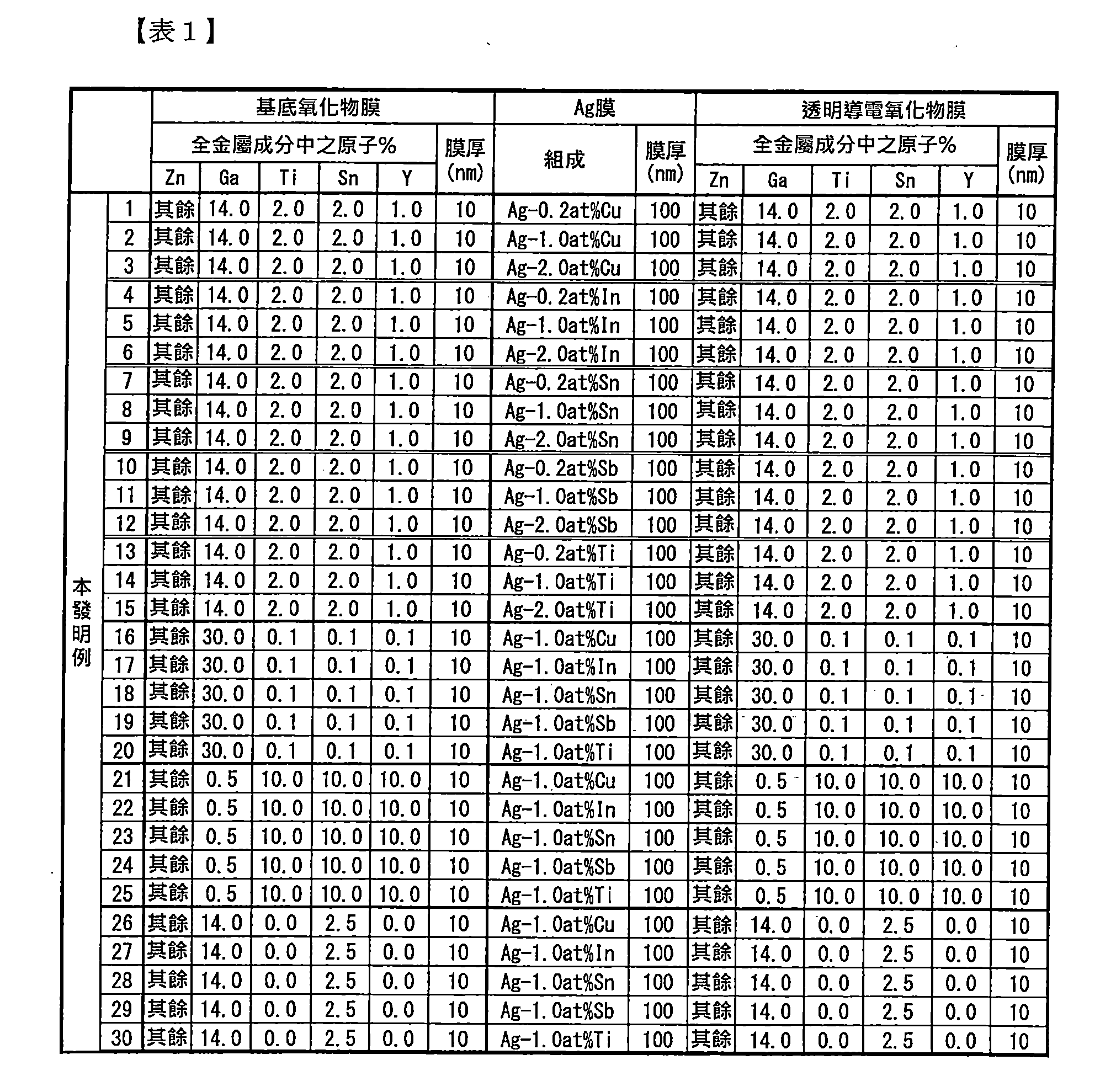
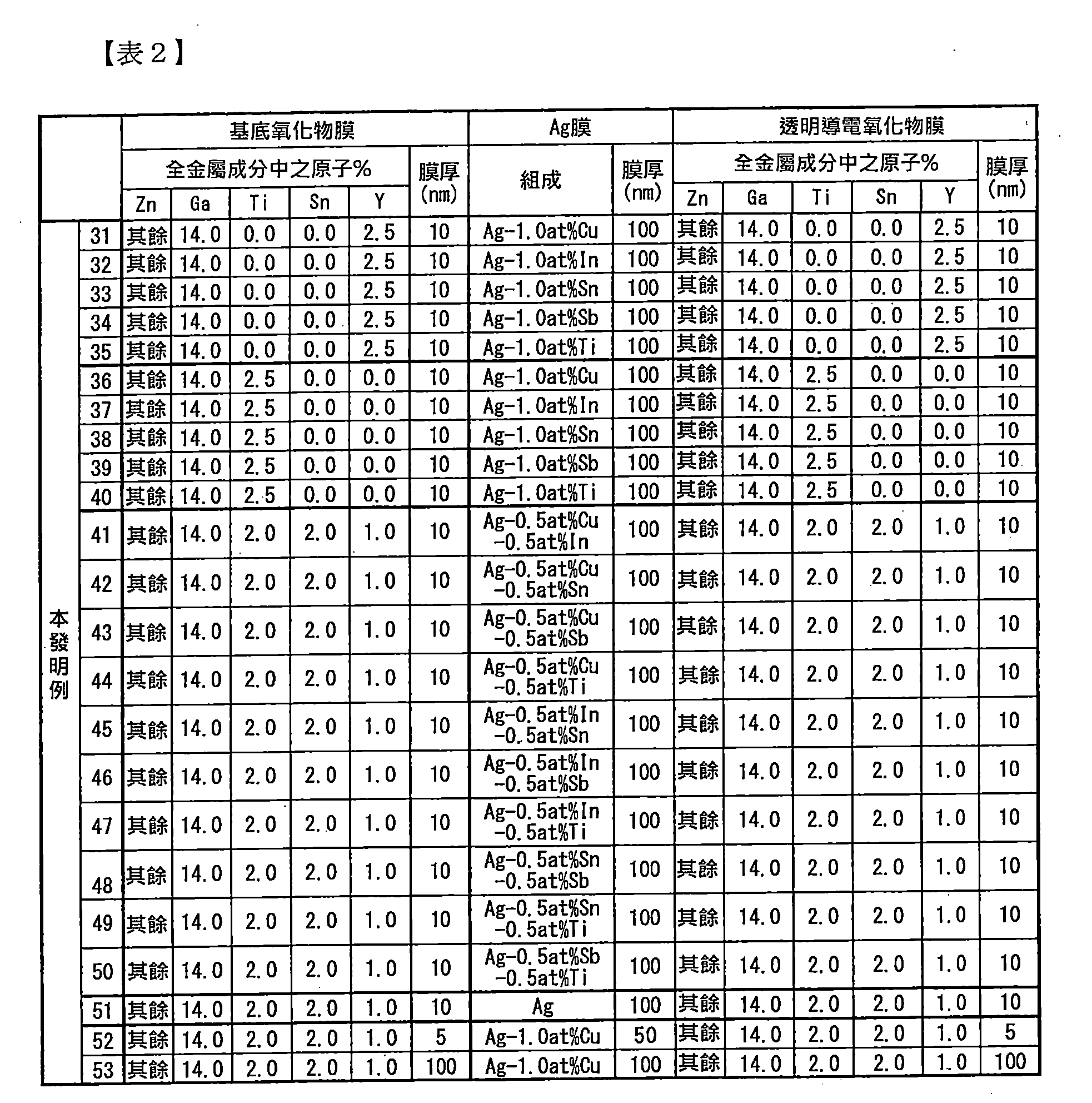
在玻璃基板(無鹼玻璃:50mm×50mm×1mmt)之表面上,藉由濺鍍法將表1-5所表示之構造之層合反射電極膜進行成膜。 On the surface of a glass substrate (alkali-free glass: 50 mm × 50 mm × 1 mmt), a laminated reflective electrode film of the structure shown in Table 1-5 was formed by sputtering.
尚,本發明之實施例及比較例中之Ag膜及透明導電氧化物膜的膜厚,係使用膜厚計(Ulvac公司製DEKTAK)來進行測定。 Further, the film thicknesses of the Ag film and the transparent conductive oxide film in the examples and comparative examples of the present invention were measured using a film thickness meter (DEKTAK manufactured by Ulvac Co., Ltd.).
又,透明導電氧化物膜及Ag合金膜的組成,係藉由使用ICP發光分光裝置(Hitachi High-Tech Science公司製ICP發光分光分析裝置STS-3500DD)來進行元素的定量分析而可求出。 In addition, the composition of the transparent conductive oxide film and the Ag alloy film can be determined by quantitative analysis of an element using an ICP emission spectrometer (ICP-based spectroscopic analyzer STS-3500DD manufactured by Hitachi High-Tech Science Co., Ltd.).
基底氧化物膜與透明導電氧化物膜之製作,係使用表1-5所記載之組成之氧化物燒結體靶材。 For the production of the base oxide film and the transparent conductive oxide film, an oxide sintered body target having the composition described in Table 1-5 was used.
Ag膜之製作,係使用表1-5所記載之組成的純Ag或 Ag合金靶材。 For the production of Ag film, pure Ag or the composition described in Table 1-5 is used. Ag alloy target.
尚,比較例中,於表5之ITO膜(In2O3中添加Sn而成的氧化物)的組成係In:35.6原子%、Sn:3.6原子%、O:60.8原子%。又,作為比較例,雖未記載於表中,但亦依造比較例1~5的構成以GZO膜(膜的組成係Zn:47.3原子%、Ga:2.2原子%、O:50.5原子%)取代ITO膜,來製作層合反射電極膜。 In the comparative example, the composition of the ITO film (the oxide in which Sn is added to In 2 O 3 ) in Table 5 is: 35.6 at%, Sn: 3.6 at%, and O: 60.8 at%. Further, although not described in the table as a comparative example, a GZO film was formed according to the structures of Comparative Examples 1 to 5 (the composition of the film: Zn: 47.3 atom%, Ga: 2.2 atom%, and O: 50.5 atom%). A laminated reflective electrode film was produced instead of the ITO film.
分別的膜之成膜條件係如下述般。 The film formation conditions of the respective films are as follows.
濺鍍裝置:DC磁電濺鍍裝置(Ulvac公司製CS-200) Sputtering device: DC magnetoelectric sputtering device (CS-200 manufactured by Ulvac)
磁界強度:1000Gauss(靶材正上方、垂直成分) Magnetic boundary strength: 1000Gauss (directly above the target, vertical component)
到達真空度:5×10⁻⁵Pa以下 The degree of vacuum reached: 5 × 10 -5 Pa or less
濺鍍氣體:Ar+O2的混合氣體(O2的混合比2%) Sputtering gas: mixed gas of Ar+O 2 (mixing ratio of O 2 is 2%)
濺鍍氣體壓:0.4Pa Sputter gas pressure: 0.4Pa
濺鍍功率:DC100W Sputtering power: DC100W
濺鍍裝置:DC磁電濺鍍裝置(Ulvac公司製CS-200) Sputtering device: DC magnetoelectric sputtering device (CS-200 manufactured by Ulvac)
磁界強度:1000Gauss(靶材正上方、垂直成分) Magnetic boundary strength: 1000Gauss (directly above the target, vertical component)
到達真空度:5×10⁻⁵Pa以下 The degree of vacuum reached: 5 × 10 -5 Pa or less
濺鍍氣體:Ar Sputtering gas: Ar
濺鍍氣體壓:0.5Pa Sputter gas pressure: 0.5Pa
濺鍍功率:DC100W Sputtering power: DC100W
對於所得到之層合反射電極膜,評估薄片電阻、反射率。 The sheet resistance and reflectance of the obtained laminated reflective electrode film were evaluated.
又,對於所得到之層合反射電極膜,進行藉由蝕刻法之圖型化試驗、及、藉由剝離法之圖型化試驗。 Further, the obtained laminated reflective electrode film was subjected to a patterning test by an etching method and a patterning test by a lift-off method.
評估方法係如下述般。 The evaluation method is as follows.
使用表面電阻測定器(三菱油化公司製Loresta AP MCP-T400),藉由四探針法來測定薄片電阻。將測定結果分別表示於表6-10中。 The sheet resistance was measured by a four-probe method using a surface resistance measuring instrument (Loresta AP MCP-T400 manufactured by Mitsubishi Petrochemical Co., Ltd.). The measurement results are shown in Tables 6-10, respectively.
使用分光光度計(Hitachi High-Technologies公司製U4100),測定從400nm至800nm的波長範圍中之反射率頻譜,可求出藍色區域(400~500nm)、及可見光區域(400~800nm)之平均反射率。將測定結果分別表示於表6-10中。 Using a spectrophotometer (U4100 manufactured by Hitachi High-Technologies Co., Ltd.), the reflectance spectrum in the wavelength range from 400 nm to 800 nm was measured, and the average of the blue region (400 to 500 nm) and the visible region (400 to 800 nm) was obtained. Reflectivity. The measurement results are shown in Tables 6-10, respectively.
對於上述之層合反射電極膜,藉由光刻法(光微影法),將阻劑膜以成為線寬/間距寬:30μm/30μm的電極圖型狀之方式形成在層合反射電極膜之上。將包含磷 酸、乙酸的混合液(關東化學公司製SEA-5)使用作為蝕刻液,並將此者進行一次性蝕刻。尚,蝕刻係在無加熱下分別以適當的蝕刻時間(20秒至240秒)來進行。又,將混合液中之磷酸的含量設為55體積%以下、乙酸的含量設為30體積%以下。 In the laminated reflective electrode film described above, the resist film is formed on the laminated reflective electrode film by photolithography (photolithography) in the form of an electrode pattern having a line width/pitch width of 30 μm/30 μm. Above. Will contain phosphorus A mixed solution of acid and acetic acid (SEA-5 manufactured by Kanto Chemical Co., Ltd.) was used as an etching liquid, and this was subjected to one-time etching. Still, the etching is performed with no appropriate heating time (20 seconds to 240 seconds). Further, the content of the phosphoric acid in the mixed solution is 55 vol% or less, and the content of acetic acid is 30 vol% or less.
之後,使用鹼性的阻劑除去液(pH9、東京應化工業公司製TOK-104)來除去阻劑膜後,藉由光學顯微鏡(KEYENCE公司製雷射顯微鏡VK-X200),以倍率50倍來觀察所形成的電極圖型,並確認透明導電氧化物膜13的殘渣之有無。尚,若可確認到未被蝕刻並以針狀或粒狀等的形狀殘留的透明導電氧化物膜之存在之情形時,則判斷存有透明導電氧化物膜13的殘渣,除此之外則判斷未有透明導電氧化物膜13的殘渣。 After that, an alkaline resist removal liquid (pH 9, TOK-104, manufactured by Tokyo Ohka Kogyo Co., Ltd.) was used to remove the resist film, and then an optical microscope (a laser microscope VK-X200 manufactured by Keyence Corporation) was used at a magnification of 50 times. The electrode pattern formed was observed, and the presence or absence of the residue of the transparent conductive oxide film 13 was confirmed. When it is confirmed that the transparent conductive oxide film which is not etched and remains in the shape of a needle or a granule is present, it is judged that the residue of the transparent conductive oxide film 13 is present, and otherwise It is judged that the residue of the transparent conductive oxide film 13 is not present.
又,使用掃描電子顯微鏡(Hitachi High-Technologies公司製SU8000),以倍率50000倍來觀察於除去阻劑膜前之電極圖型的截面(與線及間距正交的垂直於基板20的成膜面的截面)。使用以本發明例2所成膜之層合反射電極膜,將經圖型化試驗後所得到之電極圖型之截面形狀之觀察結果表示於圖7。如圖7所表示般,測量被蝕刻至阻劑膜41的內部為止的Ag膜12的長度L1與透明導電氧化物膜13的長度L2,並算出長度L1與長度L2的差來作為過度蝕刻的長度。尚,長度L1係與基板20的成膜面呈平行的方向之阻劑膜41的端部與Ag膜12的端部之間的長度,長度L2係與基板20的成膜面呈平行的方向之阻劑膜 41的端部與透明導電氧化物膜13的端部之間的長度。將在與基板20之間本來應該殘留著層合反射電極膜10之阻劑圖型的邊界部(邊緣部)作為阻劑膜41的端部,將在阻劑圖型與基板20之間殘留的層合反射電極膜10之Ag膜12的端部作為Ag膜12的端部,將殘留的層合反射電極膜10之透明導電氧化物膜13的端部作為透明導電氧化物膜13的端部,並測定長度L1、L2。將本發明例及比較例之各樣品之過度蝕刻的長度分別表示於表6-10中。尚,表6-10之過度蝕刻的長度係觀察1個截面所得到之值。 Further, a scanning electron microscope (SU8000 manufactured by Hitachi High-Technologies Co., Ltd.) was used to observe a cross section of the electrode pattern before the removal of the resist film at a magnification of 50,000 times (a film forming surface perpendicular to the substrate 20 perpendicular to the line and the pitch) Cross section). The observation result of the cross-sectional shape of the electrode pattern obtained by the patterning test was shown in Fig. 7 using the laminated reflective electrode film formed by the film of the present invention. As indicated in FIG. 7, the internal measurement is etched to a resist film 41 Ag film 12 until the length L 1 of the transparent conductive oxide film 13 is L 2, and calculates the difference between the length L 1 and length L 2 to As the length of over-etching. Further, the length L 1 is a length between the end portion of the resist film 41 and the end portion of the Ag film 12 in a direction parallel to the film formation surface of the substrate 20, and the length L 2 is parallel to the film formation surface of the substrate 20. The length between the end of the resist film 41 and the end of the transparent conductive oxide film 13 in the direction. The boundary portion (edge portion) of the resist pattern in which the laminated reflective electrode film 10 should originally remain between the substrate 20 and the substrate 20 is used as the end portion of the resist film 41, and remains between the resist pattern and the substrate 20. The end portion of the Ag film 12 of the laminated reflective electrode film 10 serves as an end portion of the Ag film 12, and the end portion of the transparent conductive oxide film 13 of the remaining laminated reflective electrode film 10 is used as the end of the transparent conductive oxide film 13. And measure the lengths L 1 and L 2 . The lengths of over-etching of each of the samples of the inventive examples and comparative examples are shown in Tables 6-10, respectively. Further, the length of the over-etching of Table 6-10 is the value obtained by observing one section.
首先,將阻劑液塗布至基板上,設置形成有線寬/間距寬:30μm/30μm的電極圖型的光罩,以曝光機照射紫外線後,用顯影液除去被感光的部分,並藉由光刻法來形成反轉圖型。 First, a resist liquid is applied onto a substrate, and a mask having an electrode pattern of a line width/space width of 30 μm/30 μm is formed, and after exposure to ultraviolet rays by an exposure machine, the photosensitive portion is removed by a developing solution, and light is removed by light. Engraving to form an inverse pattern.
接下來,在形成有反轉圖型的基板上,使用如上述般的濺鍍裝置來將層合反射電極膜進行成膜。 Next, a laminated reflective electrode film was formed on the substrate on which the inverted pattern was formed by using a sputtering apparatus as described above.
接下來,浸漬在阻劑除去液(pH9、東京應化工業公司製TOK-104)中,除去在阻劑膜上所成膜的層合反射電極膜後,藉由光學顯微鏡(KEYENCE公司製雷射顯微鏡VK-X200),以倍率50倍來觀察所形成的電極圖型,並確認電極圖型的精度。尚,在線(P)中可確認到膜的剝離或阻劑的殘渣之情形時,則判斷為無法精度良好地形成 電極圖型,除此之外則判斷為可精度良好地形成電極圖型。 Next, it was immersed in a resist removal liquid (pH 9, TOK-104, manufactured by Tokyo Ohka Kogyo Co., Ltd.), and the laminated reflective electrode film formed on the resist film was removed, and then subjected to an optical microscope (Lightning by KEYENCE Corporation). The microscope VK-X200) was used to observe the formed electrode pattern at a magnification of 50 times, and the accuracy of the electrode pattern was confirmed. When the film peeling or the residue of the resist is confirmed in the line (P), it is judged that the film cannot be formed accurately. In addition to the electrode pattern, it was judged that the electrode pattern can be formed with high precision.


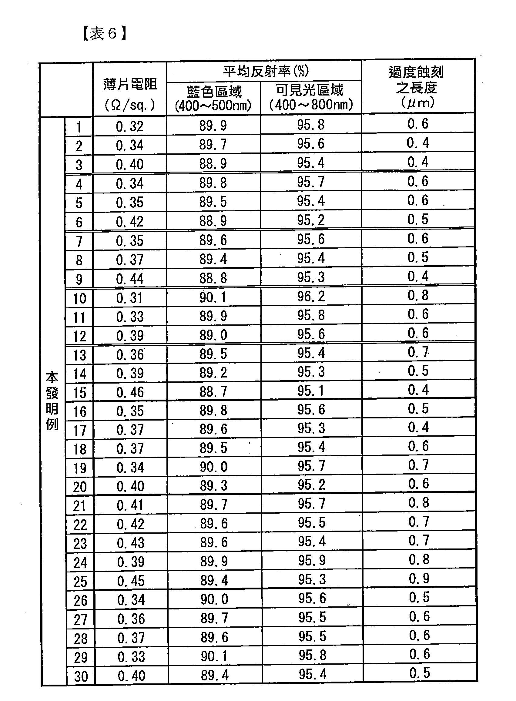

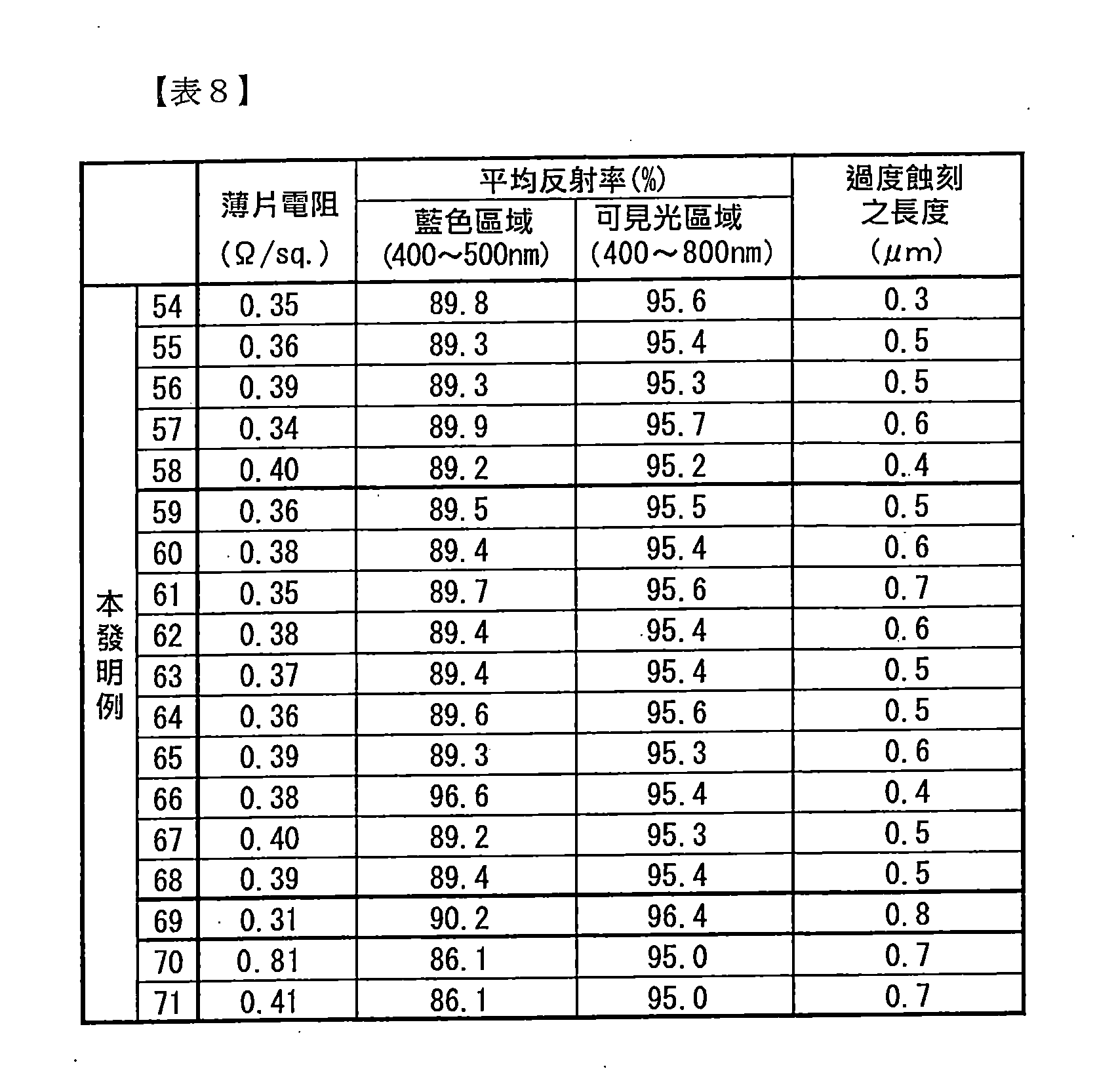


如表6-10所表示般,可確認本發明例中,藍色區域之平均反射率、可見光區域之平均反射率皆分別為86%、95%以上,進而,成膜後薄片電阻除了Ag膜的厚度為50nm的樣品(本發明例52、本發明例70)以外,皆為0.5Ω/sq.以下,故可得到反射率為優異、且電阻充分低的層合膜。本發明例52及70中,因為Ag膜的膜厚為50nm太薄的緣故,薄片電阻係成為0.8Ω/sq.左右之值,反射率也些許變小。又,本發明例53及71中,因為Ag膜上之透明導電氧化物膜的膜厚為100nm太厚而致使吸 收增加的緣故,相較於10nm的樣品而言反射率為些許變小。 As shown in Table 6-10, it was confirmed that in the examples of the present invention, the average reflectance of the blue region and the average reflectance of the visible light region were 86% and 95%, respectively, and further, the sheet resistance after film formation was except for the Ag film. The sample having a thickness of 50 nm (Example 52 of the present invention and Example 70 of the present invention) was 0.5 Ω/sq. or less, and thus a laminated film having excellent reflectance and sufficiently low electric resistance was obtained. In Examples 52 and 70 of the present invention, since the film thickness of the Ag film was too thin at 50 nm, the sheet resistance was about 0.8 Ω/sq., and the reflectance was somewhat small. Further, in Examples 53 and 71 of the present invention, since the film thickness of the transparent conductive oxide film on the Ag film was too large to be 100 nm, the absorption was caused. As a result of the increase, the reflectance is somewhat smaller than that of the 10 nm sample.
另一方面,比較例中,藍色區域之平均反射率、可見光區域之平均反射率皆分別小於86%、95%,故與本發明例相較為低。 On the other hand, in the comparative example, the average reflectance of the blue region and the average reflectance of the visible light region were each less than 86% and 95%, respectively, and thus it was lower than the example of the present invention.
又,藉由蝕刻法之圖型化試驗之結果,如圖7、表6-9所表示般,本發明例之層合膜的過度蝕刻的長度為1μm以下,確認到可精度良好地形成未有透明導電氧化物膜的殘渣之配線圖型。 In addition, as shown in Fig. 7 and Table 6-9, the length of the over-etching of the laminated film of the example of the present invention is 1 μm or less, and it is confirmed that the film can be accurately formed without any result as shown in Fig. 7 and Table 6-9. A wiring pattern of a residue having a transparent conductive oxide film.
另一方面,如表10所表示般,比較例之層合膜的過度蝕刻的長度皆大於1μm,又,亦產生透明導電氧化物膜的殘渣,難以藉由進行一次性蝕刻而精度良好地形成層合反射電極圖型。 On the other hand, as shown in Table 10, the length of the over-etching of the laminated film of the comparative example was more than 1 μm, and the residue of the transparent conductive oxide film was also generated, and it was difficult to form it with high precision by performing one-time etching. Laminated reflective electrode pattern.
又,藉由剝離法之圖型化試驗之結果可確認,本發明例係可精度良好地形成電極圖型。 Moreover, as a result of the patterning test by the peeling method, it was confirmed that the electrode pattern can be accurately formed in the example of the present invention.
又,用目視來觀察剝離阻劑後之電極圖型的表面時,本發明例係與試驗前相比未發現變化,相較於此,以未添加Sn、Y、Ti的GZO膜來作為透明導電氧化物之比較例之層合膜,則於阻劑剝離後可觀察到多處的膜剝落。 Further, when the surface of the electrode pattern after peeling off the resist was visually observed, the examples of the present invention were not changed as compared with those before the test, and the GZO film to which Sn, Y, and Ti were not added was used as the transparent. In the laminated film of the comparative example of the conductive oxide, a plurality of film peelings were observed after the resist was peeled off.
由上述內容可確認,依據本發明例將可提供可見光區域、特別是藍色區域的反射率為高、電阻值為低、且可形成微細圖型之層合反射電極膜。 As described above, according to the present invention, it is possible to provide a laminated reflective electrode film having a high reflectance of a visible light region, particularly a blue region, a low resistance value, and a fine pattern.
本發明之層合反射電極膜係因可見光區域、特別是藍色區域的的反射率為高、電阻值為低、且藉由蝕刻法可容易地形成微細的電極圖型,故適合於例如有機電致發光(EL)元件的陽極。 The laminated reflective electrode film of the present invention is suitable for, for example, having a high reflectance in a visible light region, particularly a blue region, a low resistance value, and a fine electrode pattern can be easily formed by an etching method. The anode of an electroluminescent (EL) element.
10‧‧‧層合反射電極膜 10‧‧‧Laminated reflective electrode film
11‧‧‧基底氧化物膜 11‧‧‧Base oxide film
12‧‧‧Ag膜 12‧‧‧Ag film
13‧‧‧透明導電氧化物膜 13‧‧‧Transparent Conductive Oxide Film
20‧‧‧基板 20‧‧‧Substrate
t1、t2、t3‧‧‧厚度 T1, t2, t3‧‧‧ thickness
Claims (10)
Applications Claiming Priority (4)
| Application Number | Priority Date | Filing Date | Title |
|---|---|---|---|
| JP2016059097 | 2016-03-23 | ||
| JP2016-059097 | 2016-03-23 | ||
| JP2017024269A JP6776931B2 (en) | 2016-03-23 | 2017-02-13 | Manufacturing method of laminated reflective electrode film, laminated reflective electrode pattern, laminated reflective electrode pattern |
| JP2017-024269 | 2017-02-13 |
Publications (2)
| Publication Number | Publication Date |
|---|---|
| TW201803409A true TW201803409A (en) | 2018-01-16 |
| TWI722146B TWI722146B (en) | 2021-03-21 |
Family
ID=60007631
Family Applications (1)
| Application Number | Title | Priority Date | Filing Date |
|---|---|---|---|
| TW106109573A TWI722146B (en) | 2016-03-23 | 2017-03-22 | Multilayer reflective electrode film, multilayer reflective electrode pattern, and method of manufacturing multilayer reflective electrode pattern |
Country Status (6)
| Country | Link |
|---|---|
| US (1) | US10971695B2 (en) |
| EP (1) | EP3435741B1 (en) |
| JP (1) | JP6776931B2 (en) |
| KR (1) | KR102327961B1 (en) |
| CN (1) | CN108886857B (en) |
| TW (1) | TWI722146B (en) |
Cited By (1)
| Publication number | Priority date | Publication date | Assignee | Title |
|---|---|---|---|---|
| TWI847680B (en) * | 2022-10-26 | 2024-07-01 | 瀚宇彩晶股份有限公司 | Display panel |
Families Citing this family (8)
| Publication number | Priority date | Publication date | Assignee | Title |
|---|---|---|---|---|
| JP6888318B2 (en) * | 2016-03-23 | 2021-06-16 | 三菱マテリアル株式会社 | Method for manufacturing laminated transparent conductive film, laminated wiring film and laminated wiring film |
| JP2020090707A (en) | 2018-12-05 | 2020-06-11 | 三菱マテリアル株式会社 | Metal film and sputtering target |
| JP2020090706A (en) | 2018-12-05 | 2020-06-11 | 三菱マテリアル株式会社 | Metal film and sputtering target |
| JP2020090708A (en) | 2018-12-05 | 2020-06-11 | 三菱マテリアル株式会社 | Metal film and sputtering target |
| CN109524575A (en) * | 2018-12-05 | 2019-03-26 | 武汉华星光电半导体显示技术有限公司 | The production method and OLED display panel of OLED display panel |
| EP3958291A1 (en) * | 2020-08-21 | 2022-02-23 | Ams Ag | Method for forming a lift-off mask structure |
| CN113054142B (en) * | 2021-04-02 | 2023-01-31 | 深圳市芯视佳半导体科技有限公司 | Silicon-based OLED micro-display anode and preparation method and application thereof |
| CN118057597A (en) * | 2022-11-18 | 2024-05-21 | 瀚宇彩晶股份有限公司 | Etching solution and manufacturing method of display panel |
Family Cites Families (24)
| Publication number | Priority date | Publication date | Assignee | Title |
|---|---|---|---|---|
| JPH1040740A (en) * | 1996-07-26 | 1998-02-13 | Kojundo Chem Lab Co Ltd | Transparent conductive film and transparent conductive material |
| JP2000133466A (en) | 1998-10-23 | 2000-05-12 | Canon Inc | Surface modified ITO film, surface treatment method thereof, and charge injection type light emitting device using the same |
| US6559594B2 (en) | 2000-02-03 | 2003-05-06 | Semiconductor Energy Laboratory Co., Ltd. | Light-emitting device |
| JP2002363732A (en) * | 2001-03-15 | 2002-12-18 | Asahi Glass Co Ltd | Method for producing transparent conductive film and transparent substrate with transparent conductive film |
| JP4186101B2 (en) | 2002-09-04 | 2008-11-26 | ソニー株式会社 | Organic EL display device |
| JP2004156070A (en) | 2002-11-01 | 2004-06-03 | Kanto Chem Co Inc | Composition of etchant for multilayer film including transparent electroconductive film |
| JP2006098856A (en) | 2004-09-30 | 2006-04-13 | Ulvac Japan Ltd | Ag REFLECTIVE FILM AND ITS MANUFACTURING METHOD |
| JP2006294261A (en) | 2005-04-05 | 2006-10-26 | Fuji Electric Holdings Co Ltd | ORGANIC EL LIGHT EMITTING ELEMENT AND MANUFACTURING METHOD THEREOF |
| US8524123B2 (en) | 2005-09-01 | 2013-09-03 | Idemitsu Kosan Co., Ltd. | Sputtering target, transparent conductive film and transparent electrode |
| FR2924274B1 (en) | 2007-11-22 | 2012-11-30 | Saint Gobain | SUBSTRATE CARRYING AN ELECTRODE, ORGANIC ELECTROLUMINESCENT DEVICE INCORPORATING IT, AND MANUFACTURING THE SAME |
| JP5003600B2 (en) | 2008-06-13 | 2012-08-15 | 住友金属鉱山株式会社 | Oxide sintered body, target, transparent conductive film obtained using the same, and conductive laminate |
| JP4295811B1 (en) * | 2008-09-17 | 2009-07-15 | 三井金属鉱業株式会社 | Zinc oxide target |
| KR101153037B1 (en) | 2008-09-19 | 2012-06-04 | 파나소닉 주식회사 | Organic electroluminescence element and method for manufacturing same |
| KR101422362B1 (en) * | 2009-07-10 | 2014-07-22 | 가부시키가이샤 한도오따이 에네루기 켄큐쇼 | Display device, display panel and electronic appliance |
| KR101047652B1 (en) * | 2009-12-18 | 2011-07-07 | 엘지이노텍 주식회사 | Light emitting device and manufacturing method |
| KR20120123185A (en) * | 2011-04-19 | 2012-11-08 | 삼성디스플레이 주식회사 | Organic electroluminescence display device |
| JP2012246511A (en) | 2011-05-25 | 2012-12-13 | Geomatec Co Ltd | Method for manufacturing metal thin film-layered substrate and method for manufacturing capacitance type touch panel |
| KR20130000218A (en) * | 2011-06-22 | 2013-01-02 | 삼성디스플레이 주식회사 | Electrode including magnetic material and organic light emitting device using the electrode |
| JP2013105546A (en) | 2011-11-10 | 2013-05-30 | Ulvac Japan Ltd | Organic el display device, led device, solar cell and reflective film |
| WO2014099080A2 (en) * | 2012-09-26 | 2014-06-26 | University Of Florida Research Foundation, Inc. | Transparent quantum dot light-emitting diodes with dielectric/metal/dielectric electrode |
| JP6375658B2 (en) * | 2014-03-19 | 2018-08-22 | 三菱マテリアル株式会社 | Laminated film |
| JP2016040411A (en) | 2014-08-12 | 2016-03-24 | 三菱マテリアル株式会社 | LAMINATED FILM, LAMINATED WIRING FILM, AND METHOD FOR PRODUCING LAMINATED WIRING FILM |
| CN106575090B (en) * | 2014-08-25 | 2020-02-07 | 日产化学工业株式会社 | Coating composition for pattern inversion on SOC pattern |
| WO2016063169A1 (en) * | 2014-10-23 | 2016-04-28 | Semiconductor Energy Laboratory Co., Ltd. | Light-emitting element |
-
2017
- 2017-02-13 JP JP2017024269A patent/JP6776931B2/en not_active Expired - Fee Related
- 2017-03-22 EP EP17770251.1A patent/EP3435741B1/en not_active Not-in-force
- 2017-03-22 KR KR1020187025183A patent/KR102327961B1/en not_active Expired - Fee Related
- 2017-03-22 TW TW106109573A patent/TWI722146B/en not_active IP Right Cessation
- 2017-03-22 US US16/086,623 patent/US10971695B2/en not_active Expired - Fee Related
- 2017-03-22 CN CN201780018466.6A patent/CN108886857B/en not_active Expired - Fee Related
Cited By (1)
| Publication number | Priority date | Publication date | Assignee | Title |
|---|---|---|---|---|
| TWI847680B (en) * | 2022-10-26 | 2024-07-01 | 瀚宇彩晶股份有限公司 | Display panel |
Also Published As
| Publication number | Publication date |
|---|---|
| KR102327961B1 (en) | 2021-11-17 |
| TWI722146B (en) | 2021-03-21 |
| US10971695B2 (en) | 2021-04-06 |
| JP2017183274A (en) | 2017-10-05 |
| JP6776931B2 (en) | 2020-10-28 |
| EP3435741B1 (en) | 2021-09-08 |
| EP3435741A4 (en) | 2019-12-04 |
| US20190103580A1 (en) | 2019-04-04 |
| KR20180124855A (en) | 2018-11-21 |
| CN108886857A (en) | 2018-11-23 |
| CN108886857B (en) | 2021-04-02 |
| EP3435741A1 (en) | 2019-01-30 |
Similar Documents
| Publication | Publication Date | Title |
|---|---|---|
| TW201803409A (en) | Laminated reflective electrode film, laminated reflective electrode pattern, and laminated reflective electrode pattern manufacturing method | |
| US20190105872A1 (en) | Multilayer transparent conductive film, multilayer wiring film, and method of forming multilayer wiring film | |
| KR101745290B1 (en) | Ag ALLOY FILM FOR REFLECTIVE ELECTRODES, AND REFLECTIVE ELECTRODE | |
| TWI445179B (en) | A wiring structure and a manufacturing method thereof, and a display device having a wiring structure | |
| KR20150087411A (en) | Thin-film transistor and manufacturing method therefor | |
| WO2004040946A1 (en) | Multilayer body, base with wiring, organic el display device, connection terminal of organic el display device, and methods for manufacturing these | |
| JP6099940B2 (en) | Display device | |
| JP2016524304A (en) | Electrode laminate and organic light emitting device | |
| TW201841403A (en) | Electrode for organic electroluminescence element, organic electroluminescence element, organic electroluminescence display device, and method for manufacturing electrode for organic electroluminescence element | |
| JP6870332B2 (en) | Method for manufacturing laminated transparent conductive film, laminated wiring film and laminated wiring film | |
| CN102610760B (en) | light emitting device | |
| CN112018260B (en) | Reflective anode electrode, thin film transistor, organic EL display, and sputtering target | |
| CN101365816B (en) | Al-Ni-B alloy material for reflective film | |
| CN104081879B (en) | Electronic installation and its manufacture method | |
| WO2017164211A1 (en) | Laminated reflective electrode film, laminated reflective electrode pattern, and method for producing laminated reflective electrode pattern | |
| WO2016111202A1 (en) | Multilayer film | |
| TW201637840A (en) | Multilayer film | |
| WO2017131183A1 (en) | Multilayer transparent conductive film, multilayer wiring film and method for producing multilayer wiring film | |
| WO2017164209A1 (en) | Laminated transparent conductive film, laminated wiring film, and method for producing laminated wiring film | |
| KR20190076494A (en) | Etching solution composition for silver-containing layer and manufacturing method for an array substrate for display device using the same | |
| JP6123285B2 (en) | Laminated film |
Legal Events
| Date | Code | Title | Description |
|---|---|---|---|
| MM4A | Annulment or lapse of patent due to non-payment of fees |