KR900008072B1 - Display - Google Patents
Display Download PDFInfo
- Publication number
- KR900008072B1 KR900008072B1 KR1019870006972A KR870006972A KR900008072B1 KR 900008072 B1 KR900008072 B1 KR 900008072B1 KR 1019870006972 A KR1019870006972 A KR 1019870006972A KR 870006972 A KR870006972 A KR 870006972A KR 900008072 B1 KR900008072 B1 KR 900008072B1
- Authority
- KR
- South Korea
- Prior art keywords
- display
- light emitting
- data
- unit
- module
- Prior art date
- Legal status (The legal status is an assumption and is not a legal conclusion. Google has not performed a legal analysis and makes no representation as to the accuracy of the status listed.)
- Expired
Links
Images


Classifications
-
- H—ELECTRICITY
- H04—ELECTRIC COMMUNICATION TECHNIQUE
- H04N—PICTORIAL COMMUNICATION, e.g. TELEVISION
- H04N9/00—Details of colour television systems
- H04N9/12—Picture reproducers
- H04N9/31—Projection devices for colour picture display, e.g. using electronic spatial light modulators [ESLM]
-
- G—PHYSICS
- G06—COMPUTING OR CALCULATING; COUNTING
- G06F—ELECTRIC DIGITAL DATA PROCESSING
- G06F3/00—Input arrangements for transferring data to be processed into a form capable of being handled by the computer; Output arrangements for transferring data from processing unit to output unit, e.g. interface arrangements
- G06F3/14—Digital output to display device ; Cooperation and interconnection of the display device with other functional units
- G06F3/1423—Digital output to display device ; Cooperation and interconnection of the display device with other functional units controlling a plurality of local displays, e.g. CRT and flat panel display
- G06F3/1446—Digital output to display device ; Cooperation and interconnection of the display device with other functional units controlling a plurality of local displays, e.g. CRT and flat panel display display composed of modules, e.g. video walls
-
- G—PHYSICS
- G09—EDUCATION; CRYPTOGRAPHY; DISPLAY; ADVERTISING; SEALS
- G09F—DISPLAYING; ADVERTISING; SIGNS; LABELS OR NAME-PLATES; SEALS
- G09F9/00—Indicating arrangements for variable information in which the information is built-up on a support by selection or combination of individual elements
- G09F9/30—Indicating arrangements for variable information in which the information is built-up on a support by selection or combination of individual elements in which the desired character or characters are formed by combining individual elements
- G09F9/302—Indicating arrangements for variable information in which the information is built-up on a support by selection or combination of individual elements in which the desired character or characters are formed by combining individual elements characterised by the form or geometrical disposition of the individual elements
- G09F9/3026—Video wall, i.e. stackable semiconductor matrix display modules
-
- G—PHYSICS
- G09—EDUCATION; CRYPTOGRAPHY; DISPLAY; ADVERTISING; SEALS
- G09G—ARRANGEMENTS OR CIRCUITS FOR CONTROL OF INDICATING DEVICES USING STATIC MEANS TO PRESENT VARIABLE INFORMATION
- G09G3/00—Control arrangements or circuits, of interest only in connection with visual indicators other than cathode-ray tubes
- G09G3/20—Control arrangements or circuits, of interest only in connection with visual indicators other than cathode-ray tubes for presentation of an assembly of a number of characters, e.g. a page, by composing the assembly by combination of individual elements arranged in a matrix no fixed position being assigned to or needed to be assigned to the individual characters or partial characters
- G09G3/2092—Details of a display terminals using a flat panel, the details relating to the control arrangement of the display terminal and to the interfaces thereto
-
- H—ELECTRICITY
- H04—ELECTRIC COMMUNICATION TECHNIQUE
- H04N—PICTORIAL COMMUNICATION, e.g. TELEVISION
- H04N3/00—Scanning details of television systems; Combination thereof with generation of supply voltages
- H04N3/10—Scanning details of television systems; Combination thereof with generation of supply voltages by means not exclusively optical-mechanical
- H04N3/12—Scanning details of television systems; Combination thereof with generation of supply voltages by means not exclusively optical-mechanical by switched stationary formation of lamps, photocells or light relays
-
- G—PHYSICS
- G09—EDUCATION; CRYPTOGRAPHY; DISPLAY; ADVERTISING; SEALS
- G09G—ARRANGEMENTS OR CIRCUITS FOR CONTROL OF INDICATING DEVICES USING STATIC MEANS TO PRESENT VARIABLE INFORMATION
- G09G2300/00—Aspects of the constitution of display devices
- G09G2300/04—Structural and physical details of display devices
- G09G2300/0439—Pixel structures
- G09G2300/0452—Details of colour pixel setup, e.g. pixel composed of a red, a blue and two green components
-
- G—PHYSICS
- G09—EDUCATION; CRYPTOGRAPHY; DISPLAY; ADVERTISING; SEALS
- G09G—ARRANGEMENTS OR CIRCUITS FOR CONTROL OF INDICATING DEVICES USING STATIC MEANS TO PRESENT VARIABLE INFORMATION
- G09G2360/00—Aspects of the architecture of display systems
- G09G2360/18—Use of a frame buffer in a display terminal, inclusive of the display panel
-
- G—PHYSICS
- G09—EDUCATION; CRYPTOGRAPHY; DISPLAY; ADVERTISING; SEALS
- G09G—ARRANGEMENTS OR CIRCUITS FOR CONTROL OF INDICATING DEVICES USING STATIC MEANS TO PRESENT VARIABLE INFORMATION
- G09G3/00—Control arrangements or circuits, of interest only in connection with visual indicators other than cathode-ray tubes
- G09G3/20—Control arrangements or circuits, of interest only in connection with visual indicators other than cathode-ray tubes for presentation of an assembly of a number of characters, e.g. a page, by composing the assembly by combination of individual elements arranged in a matrix no fixed position being assigned to or needed to be assigned to the individual characters or partial characters
- G09G3/22—Control arrangements or circuits, of interest only in connection with visual indicators other than cathode-ray tubes for presentation of an assembly of a number of characters, e.g. a page, by composing the assembly by combination of individual elements arranged in a matrix no fixed position being assigned to or needed to be assigned to the individual characters or partial characters using controlled light sources
-
- Y—GENERAL TAGGING OF NEW TECHNOLOGICAL DEVELOPMENTS; GENERAL TAGGING OF CROSS-SECTIONAL TECHNOLOGIES SPANNING OVER SEVERAL SECTIONS OF THE IPC; TECHNICAL SUBJECTS COVERED BY FORMER USPC CROSS-REFERENCE ART COLLECTIONS [XRACs] AND DIGESTS
- Y10—TECHNICAL SUBJECTS COVERED BY FORMER USPC
- Y10S—TECHNICAL SUBJECTS COVERED BY FORMER USPC CROSS-REFERENCE ART COLLECTIONS [XRACs] AND DIGESTS
- Y10S345/00—Computer graphics processing and selective visual display systems
- Y10S345/903—Modular display
Landscapes
- Engineering & Computer Science (AREA)
- Theoretical Computer Science (AREA)
- Multimedia (AREA)
- Physics & Mathematics (AREA)
- General Physics & Mathematics (AREA)
- Signal Processing (AREA)
- Human Computer Interaction (AREA)
- General Engineering & Computer Science (AREA)
- Computer Hardware Design (AREA)
- Control Of Indicators Other Than Cathode Ray Tubes (AREA)
Abstract
내용 없음.No content.
Description
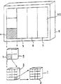
제1도는 이 발명의 한 실시예에 의한 표시장치를 표시하는 전체구성도.1 is an overall configuration diagram showing a display device according to an embodiment of the present invention.
제2도는 그 발광소자의 한예로서의 형광표시관의 구조를 표시하는 개략 단면도.2 is a schematic cross-sectional view showing the structure of a fluorescent display tube as an example of the light emitting element.
제3도는 그 제어전극의 구성을 표시하는 설명도.3 is an explanatory diagram showing the configuration of the control electrode.
제4도는 상기 표시장치의 모듈 구성을 표시하는 블록도.4 is a block diagram showing a module configuration of the display device.
제5도는 상기 표시장치의 구조를 표시하는 일부 절개사시도.5 is a partially cutaway perspective view showing the structure of the display device.
제6도는 상기 모듈의 제어회로구성을 표시하는 블록도.6 is a block diagram showing a control circuit configuration of the module.
제7도는 이 발명의 다른 실시예에 의한 표시장치의 요부를 표시하는 블록도7 is a block diagram showing the main parts of a display device according to another embodiment of the present invention.
제8도는 상기 발광소자에 송출되는 신호의 타임차트.8 is a time chart of signals sent to the light emitting element.
제9도 및 제10도는 공통 신호선에서의 데이터 전송타이밍을 표시하는 타임차트9 and 10 are time charts showing data transfer timings on a common signal line.
제11도는 이 발명의 다른 실시예에 의한 모듈제어회로를 표시하는 블록도.11 is a block diagram showing a module control circuit according to another embodiment of the present invention.
제12도는 이 발명의 대상이 되는 표시부를 나타내는 도.12 is a view showing a display unit which is the object of this invention.
제13도는 제11도 표시제어부의 블록도.13 is a block diagram of a display control unit of FIG.
제14도는 유닛의 제어회로 일부를 표시하는 블록도.14 is a block diagram showing a part of a control circuit of a unit.
제15, 제17, 제18도는 또 다른 실시예의 타임차트.15, 17, and 18 are time charts of yet another embodiment.
제16도는 이 발명의 응용도.16 is an application of this invention.
제19도는 종래의 표시장치의 구성도.19 is a block diagram of a conventional display device.
제20도는 제19도의 제어장치 및 스크린의 블록도.FIG. 20 is a block diagram of the controller and screen of FIG. 19. FIG.
* 도면의 주요부분에 대한 부호의 설명* Explanation of symbols for main parts of the drawings
1 : 발광소자 2 : 발광부1: light emitting element 2: light emitting portion
3 : 유닛 4 : 모듈3: unit 4: module
5 : 모듈군 15 : 프레임메모리5: Module Group 15: Frame Memory
16 : 온·오프판정부 17 : 타이밍제어부16: On / Off Determination 17: Timing Control Unit
18 : 어드레스 제어부 30 : 스크린18: address control unit 30: screen
이 발명은 발광소자를 다수 배열구성하고 옥외경기장등을 중심으로 이용되고 있는 대화면의 표시장치에 관한 것이다.BACKGROUND OF THE
이 종류의 대화면 표시장치는 종래 CRT 혹은 전구를 사용한 단화소(single picture element) 발광소자를 다수 배열하므로서 표시부가 구성되는 것이 일반적이며 천연색 표시를 하는 표시장치는 적, 녹, 청 3종류의 단화소 발광소자를 규칙적으로 배열한 것, 혹은 적, 녹, 청의 3색을 포함한 단화소 발광소자를 다수 배열한 것이 있었다.In this type of large screen display device, a display unit is generally constructed by arranging a plurality of single picture element light emitting elements using a CRT or a light bulb, and a display device for displaying color in three colors is red, green, and blue. Some light emitting devices were arranged regularly, or a plurality of single pixel light emitting devices including three colors of red, green, and blue were arranged.
이들의 표시장치는 복수의 발광소자와 이들을 구동하는 전자회로로서 유닛을 구성하고 이와같은 유닛을 다수 배열한 표시장치와 표시를 제어하는 제어장치 및 전원장치로서 구성되는 것이며 제19도는 이와같은 종래의 표시장치의 일례를 표시하는 구성도이다.These display devices are constituted by a plurality of light emitting elements and electronic circuits driving them, and are constituted by a display device in which a large number of such units are arranged, a control device for controlling display, and a power supply device. It is a block diagram which shows an example of a display apparatus.
이 도면에서, 30은 이 표시장치의 스크린, 3은 이 스크린(30)의 구성요소로서의 유닛, 6은 복수의 유닛(3)을 수용하여 스크린을 구성하고 있는 프레임이며, 13은 전원, 29는 스크린(30)의 각 유닛(3)을 제어하는 표시제어부이다. 또 제20도는 이 표시제어부(29)의 구성을 표시하는 블록도이며 도면에서 26은 입력된 비데오신호를 디지탈 신호로 변환하는 아날로그.디지탈변환기(이하 A/D변환기라함), 15는 디지탈화된 비데오신호를 저장하는 프레임메모리, 16은 프레임메모리(15)에 접속된 온·오프 판정부, 27은 온·오프 판정부(l6)에 접속되어 스크린(30)의 열선택을 행하는 열선택회로, 28은 스크린(30)의 행선택을 행하는 행선택회로, 18은 이 행선택회로(28)와 상기 프레임메모리(15)의 어드레스 제어를 행하는 어드레스제어부, 22는 이 어드레스 제어부(18)와 상기 A/D변환기(26)의 타이밍을 제어하는 타이밍제어부, 32는 복수개가 격자상으로 배열되어서 상기 유닛(3)을 형성하는 단화소 발광소자이다.In this figure, 30 is a screen of this display device, 3 is a unit as a component of this
다음은 동작에 관하여 설명한다.The following describes the operation.
이 표시장치에 입력된 비데오신호는 A/D변환기(26)에 의하여 소정의 디지탈신호로 변환되어 프레임메모리(15)에 저장된다. 프레임메모리(15)에 저장된 데이터는 단화상소자의 발광소자(32)에 대응한 어드레스에 따라서 판독되어 순차 온·오프신호로 변환되고 열선택회로(27) 및 행선택회로(28)에 의하여 지정되는 단화소 발광소자(32)에 공급된다. 각 단화소 발광소자(32)는 각각 기억기능을 갖추고 있으며 단화소 발광소자(32)에 공급된 온·오프 신호는 재차신호가 공급되기까지 유지된다. 프레임메모리(15)의 내용은 각 피일드(field)가 복수회 판독되어 각각 소정의 온·오프신호로 변환되어서 표시되며 1피일드내의 온시간의 누적치가 그 단화소 발광소자(32)의 표시할 비데오신호의 진폭에 비례한 것이된다.The video signal inputted to the display device is converted into a predetermined digital signal by the A /
한편, 스크린(30)은 유닛(3)의 배열방법에 따라 각종 규격구성이 가능하며 제어장치(29)는 여러가지 스크린 규격을 제어할 수 있다.Meanwhile, the
즉 발광부가 k×1의 격자배열로된 복수화소의 발광소자를 사용하여 발광소자를 기판상에 구동회로와 함께 m×n의 격자배열로하여 유닛(3)을 형성하고 또한 이와같은 유닛(3)을 p×q의 격자상으로 배열하여 이들의 유닛을 제어하는 표시제어부(29) 및 전원(13)과 더불어 모듈을 형성하고 이 모듈을 복수개 배열하여서 스크린을 구성하고 있다.That is, the light emitting unit uses a plurality of pixel light emitting elements having a k × 1 lattice arrangement to form the
종래의 표시장치는 이상과 같이 구성되어 있으므로 높은 해상도를 얻기 위하여는 보다 소형의 단화소 발광소자를 고밀도로 배열할 필요가 있으며 그때문에 사용되는 단화소 발광소자의 수는 크게 불어나고 그에 따라 구동회로 기타의 주변회로도 비약적으로 증가하는 반면 단화소 발광소자의 소형화에 의한 원가절감은 보잘것 없는 것이며 구동회로등의 주변회로에도 동등한 것을 사용하는 것이기 때문에 고해상도화와 저가격화, 경량, 박형화를 동시에 실현하는 것이 극히 곤란하다는 문제점이 있었다.Since the conventional display device is constructed as described above, in order to obtain a high resolution, it is necessary to arrange smaller single pixel light emitting elements at a high density, and therefore, the number of single pixel light emitting elements used is greatly increased, and thus the driving circuit While other peripheral circuits also increase dramatically, cost savings due to miniaturization of single pixel light emitting devices are insignificant, and equivalent circuits are also used for peripheral circuits such as driving circuits. Therefore, high resolution, low cost, light weight, and thinness are simultaneously realized. There was a problem that was extremely difficult.
또 종래의 표시장치는 대화면화 혹은 고해상도화를 위하여 화소수를 증가한 경우나 표시품질 향상을 위해 각 화소의 보유하는 데이터량이 증가한 경우등에는 소요시간내에 프레임메모리의 판독회수가 증가하여 프레임메모리의 접근시간에 맞지 않게된다는 등의 문제점이 있었다.In the conventional display device, when the number of pixels is increased for large screen or high resolution, or when the amount of data held by each pixel is increased to improve display quality, the number of readings of the frame memory is increased within the required time to access the frame memory. There was a problem such as not being in time.
또한 메모리에 저장된 디지탈 데이터를 소정의 시간폭에 변환한다는 처리는 표시장치로서의 가장 중요한 신호처리의 하나이며 종래 1개소에 집중하고 있던 신호처리부를 모듈마다 분할하므로서 오히려 고가의 장치가 된다는 문제점이 있었다.In addition, the process of converting the digital data stored in the memory to a predetermined time width is one of the most important signal processings as a display device, and there is a problem that it becomes a rather expensive device by dividing the signal processing unit concentrated in one module for each module.
이 발명은 상기와 같은 문제점을 해소하기 위한 것으로서 해상도가 높고 저가격이면서 엷고 가벼운 대화면의 표시장치를 얻는 것을 목적으로 한다.The present invention has been made to solve the above problems, and an object thereof is to obtain a display device having a high resolution, low cost, and a thin and light large screen.
또 이 발명은 메모리를 복수에 분할하여 병렬로 접근하므로서 제어의 효율화를 도모한 표시장치를 얻는것을 목적으로 한다.In addition, an object of the present invention is to obtain a display device in which control efficiency is achieved by dividing a plurality of memories in parallel and accessing them in parallel.
더욱이 이 발명은 단순한 회로구성으로 디지탈신호의 시간폭변환을 행할 수 있는 중간계조(half tone)화상의 표시장치릍 얻는 것을 목적으로 한다.Furthermore, an object of the present invention is to obtain a display device of a half tone image capable of converting a time width of a digital signal with a simple circuit configuration.
이 발명에 관한 표시장치는 발광부가 k×1의 격자가 배열된 복수화소의 발광소자를 사용하고 이 발광소자를 기판상에 구동회로와 함께 m×n의 격자배열로 하여서 유닛을 형성하고 또한 이와같은 유닛을 p×q의 격자상으로 배열하여 이들의 유닛을 제어하는 제어회로 및 전원과 더불어 모듈을 형성하며 이 모듈을 복수개 배열하여서 스크린을 구성한 것이다.In the display device according to the present invention, the light emitting unit uses a plurality of pixel light emitting elements in which a k × 1 lattice is arranged, and forms the unit by arranging the light emitting elements in a m × n lattice arrangement together with a driving circuit on the substrate. The same units are arranged in a grid of p × q to form a module together with a control circuit and a power supply for controlling these units, and a plurality of these modules are arranged to form a screen.
또, 이 발명에 관한 표시장치는 프레임메모리를 모듈마다에 화면상응하게 분할 배치하고 이 모듈을 2차원적으로 다수 배열함으로써 대화면의 표시장치를 구성하여 각 모듈에 고유의 어드레스를 할당하는 동시에 각모듈을 공통신호선에 접속하고 이 공통신호선을 통하여 표시데이터와 이 표시데이터를 표시할 모듈의 어드레스 데이터를 전송하는 것이다. 그리고 또한 이 발명에 관한 표시장치는 표시부의 화소수를 종으로 2a, 횡으로 2b으로 디지탈 처리상 유리하게 구성하며(a,b는 정의정수), 또한 제어회로는 화소수에 대응한 메모리와 클록(clock)을 순차 분주하는 일련의 카운터 및 데이터의 온·오프를 판정하는 비교기를 설치하여 카운터의 출력으로서 얻게되는 클록의 분구치를 메모리 어드레스 및 상기 비교기의 한쪽 입력에 할당하는 동시에 메모리에서 읽어낸 데이터를 순차 상기 카운터의 출력과 대소관계를 비교하고 얻은 대 또는 소(온 또는오프)를 표시하는 데이터를 클록에 의하여 화소에 대응하여 배열하도록 한것이다.In addition, the display device according to the present invention divides and arranges the frame memory according to the screen for each module and arranges a plurality of modules in two dimensions to form a large display device, assigning a unique address to each module, Is connected to the common signal line, and the display data and the address data of the module to display the display data are transmitted through the common signal line. In addition, the display device according to the present invention is advantageously configured in terms of digital processing with the number of pixels of the display unit being 2 a vertically and 2 b horizontally (a and b are positive integers), and the control circuit is a memory corresponding to the number of pixels. And a series of counters that sequentially divide clocks, and a comparator for determining on / off of data, and assigning a clock divider obtained as an output of the counter to a memory address and one input of the comparator, The read data is sequentially compared with the output of the counter, and the data indicating the obtained large or small (on or off) is arranged to correspond to the pixels by the clock.
이 발명에서의 표시장치는 화소로서의 발광부를 복수로 포함하는 복수화소의 발광소자를 사용하므로서 1화소당의 원가절감을 기하는 동시에 유닛, 모듈, 스크린과 각각 효율적으로 기능을 분단시켜서 저가격이며 또한 소형의 구성으로된 표시장치를 실현한다. 또 이 발명에서의 각 모듈은 공통신호선을 통하여 전송되어오는 표시데이터중에서 대응된 어드레스데이터에 기준하여 해당모듈에 할당된 표시데이터를 선택하여 수신하고 일단 각 모듈의 프레임메모리에 저장하여 각 모듈마다 표시제어를 행하며 이에 의하여 제어의 효율화를 도모한다. 그리고 또한 이 발명에서의 표시장치의 카운터는 일순(一巡)하는 사이에 각화소의 표시가 모두 온(ON)이 되는 누적시간이 대응하는 메모리의 데이터에 비례한다.The display device according to the present invention uses a plurality of light emitting elements including a plurality of light emitting units as pixels, thereby reducing costs per pixel and efficiently dividing functions into units, modules, and screens. A display device with a configuration is realized. In addition, each module of the present invention selects and receives the display data assigned to the module based on the corresponding address data among the display data transmitted through the common signal line, and stores it in the frame memory of each module for display for each module. The control is performed, whereby the control can be made more efficient. In addition, the counter of the display device of this invention is proportional to the data of the memory corresponding to the cumulative time when all of the display of each pixel is turned ON during one order.
다음은 이 발명의 한실시예를 도면에 의하여 설명한다. 제1도는 이 발명의 전체구성을 표시하는 블록도이다.The following describes one embodiment of this invention with reference to the drawings. 1 is a block diagram showing the overall configuration of this invention.
도면에서, 1은 발광소자이며 발광부(2)가 종으로 k개, 횡에 1개 (k,l는 정의 정수)의 격자상으로 배열된 것이다.In the figure, 1 is a light emitting element, and the
도면에서 k=4, 1=4의 경우를 한예로 표시하였다. 3은 이 발광소자(1)를 종에 m개, 횡에 n개(m,n는 정의정수)의 격자상에 배열하여 구성된 유닛이며 도면에서는 m=4, n=4의 경우를 한예로서 표시하였다. 4는이 유닛(3)을 종에 p개, 횡에 q개(p,q는 정의정수)의 격자상 배열로 하여 구성한 모듈이다.In the figure, the case of k = 4 and 1 = 4 is shown as an example. 3 denotes a unit in which the
도면에서는 p=2, q=2의 경우를 한예로서 표시하였다. 5는 이 모듈(4)를 종으로 배열한 모듈군, 6은 프레임이며, 30은 모듈군(5)를 프레임(6)내에 횡으로 배열하여 구성되는 스크린이다.In the figure, the case of p = 2 and q = 2 is shown as an example. 5 is a module group in which the
상기 발광소자(1)는 예를 들면 액정, 형광표시관등의 점행렬(dot nmtrix)형 표시소자이며 서로 직교하는 제1 및 제2의 2종류 제어전극을 조합하어 제어하여서 표시를 제어한다. 이어서 형광표시관을 예를 들어 설명하기로 한다.The
제2도는 이와같은 형광표시관의 내부구조를 표시하는 개략단면도이다. 9는 열전자를 방출하는 음극, 8은전자를 가속하는 그리드, 7은 형광물질이 도포된 양극이며, 10은 양극(7)에 전압을 인가하기 위한 배선, 11은 배기구, 12는 외부접속을 위한 전극이다.2 is a schematic cross-sectional view showing the internal structure of such a fluorescent display tube. 9 is a cathode for emitting hot electrons, 8 is a grid for accelerating electrons, 7 is a cathode coated with a fluorescent material, 10 is wiring for applying a voltage to the
이 형광표시관은 양극(7)에 음극(9)으로부터의 열전자가 충돌함으로써 양극(7)표면에 도포된 형광뭍질이 발광하는 것이며 양극(7)은 배선(10)에서 인가되는 전압에 의하여 제어된다.The fluorescent display tube emits a fluorescent substance coated on the surface of the
이 양극(7)이 상기 제1제어전극에 또 그리드(8)가 제2제어전극에 대응한다.The
제3도는 표시를 제어하는 제어전극의 구성을 도시하는 설명도이며 그리드(8)는 Y1∼Y4의 4개가 행방향에 공통으로, 또 양극(7)은 X1∼X4의 4개가 열방향에 공통으로 접속되어 행렬이 구성되어 있으며 직교하는 양 제어전극의 교점에 대응하여 배치된 발광부(2)의 표시가 제어된다.3 is an explanatory diagram showing the configuration of the control electrode for controlling the display. In the
전 천연색의 표시장치를 구성하는 경우는 적(R), 녹(G), 청(B)의 3종류의 형광물질을 양극에 규칙적으로 도포한 것을 사용한다.When forming a full-color display device, one which is regularly coated with three kinds of fluorescent materials of red (R), green (G), and blue (B) on the anode is used.
특히, 적, 녹, 청의 발광부(2)수가 적 : 녹 : 청=1 : 2 : 1이며, 제3도에 표시한 바와 같은 화소배열로한 경우는 해상도에 있어서 유리한 천연색 표시장치를 얻게 된다.In particular, when the number of
유닛(3)은 제1도와 같이 이와같은 형광표시관등에 의한 복수화소의 발광소자(l)와, 쉬프트레지스터(shift register), 래치(latch)등을 포함하는 그 구동회로를 기판상에 배열하여 구성한다.The
여기서 발광소자(1)의 제어전극을 상술한 바와 같이 행렬구성으로 하므로서 발광소자(1)의 외부에 인출되는 전극(12)수를 삭감할 수 있는 동시에 구동회로의 삭감을 기할 수 있으며 유닛(3)의 구성이 간소화될 수 있다. 모듈(4)은 제4도와 같이 복수의 유닛(3)과 이들을 제어하는 제어회로(31) 및 진원(13)으로 구성된다.In this case, the control electrodes of the
종래의 표시장치에서는 표시제어부(29) 혹은 전원(13)은 제19도에 표시한 바와 같이 스크린(30)외부에 집중하여 설치되며, 또 각종 규격의 스크린을 제어할 수 있도록 되어 있어 그 회로구성도 복잡하였는데 대하여 이 발명에서는 각 모듈(4)에 분산배치하여 한정된 부분밖에는 제어하지 않는다는 제한을 두므로서 제어회로(31)의 회로구성에 대하여 간소화를 도모하고 있다.In the conventional display device, the
특히 발광소자(1)에 포함되는 발광부(2)의 수(k×1), 유닛(3)이 포함하는 발광소자(1)의 수(m×n), 또한 모듈(4)이 포함하는 유닛(3)의 수(P×q)의 관계에 있어서 k=2r, l=2s(r,s는 정의정수), m=2t, n=2u, p=2v, q=2w(t,u,v,w는 부가아닌 정수)과 디지탈 신호처리상 유리한 구성으로 하므로서 제어회로(31)는 효율적으로 구성할 수 있게 된다.In particular, the number of
특히 제5도와 같이 모듈(4)을 형성하는 유닛군의 배후에 제어회로(31) 및 전원(13)을 배치함으로써 소형화 할수가 있다.In particular, as shown in FIG. 5, the
제6도는 이 제어회로(31)의 구성을 표시하는 블록도이며, 이 도면에서, 15는 프레임메모리, 16은 프레임메모리(15)에 접속된 온·오프 판정부, 19는 이 온·오프 판정부(16)에 접속되어서 유닛(3)를 선택하는 유닛 선택게이트, 18은 프레임메모리(15), 온,오프 판정부(16) 및 유닛선택게이트(19)의 어드레스제어를 행하는 어드레스제어부, 17은 이 어드레스제어부(18)의 타이밍제어를 행하는 타이밍제어부이다.FIG. 6 is a block diagram showing the structure of this
여기서 고속으로 샘플링된 디지탈 비데오신호를 그대로 평면케이블(flat cable)을 사용하여 각 모듈(4)로 전송하는 것은 곤란하기 때문에 제7도에 표시한 바와 같이 복수의 모듈(4)을 공통신호선(14)으로 접속하여 모듈군(5)을 형성하고 이 모듈군(5)을 복수배열하여 스크린(30)을 형성하고 있다.Here, since it is difficult to transfer the digital video signal sampled at high speed to each
그리고 도면에서 24 및 25는 공통신호선(14)의 버퍼(buffer) 및 종단부이며, 26은 입력되는 비데오신호를 디지탈신호로 변환하는 A/D변환기, 21은 모듈군(5) 대응으로 설치되어 A/D변환기(26)로부터의 디지탈 비데오신호를 축적하여 속도변환을 행하는 버퍼메모리, 22는 이 A/D변환기(26)과 버퍼메모리(21)의 타이밍제어를 행하는 타이밍 발생부, 20은 이들에 의하여 구성되는 신호공급수단이며 이 신호공급수단(20)은 제5도와 같이 전원을 분배하는 전원분배수단(33)과 함께 프레임(6)내에 수용되어 있다. 이어서, 동작에 대하여 설명한다.In the figure, 24 and 25 are buffers and terminations of the
입력된 비데오신호는 신호공급수단(20)의 A/D변환기(26)에 의하여 소정의 디지탈신호에 변환되어서 각 모듈군(5)에 대응하여 설치된 버퍼메모리(21)내에 일단 저장된다.The input video signal is converted into a predetermined digital signal by the A /
이 버퍼메모리(21)에 저장된 비데오신호는 저속으로 판독되어 어드레스가 부가되어서 대응하는 모듈군(5)으로 개별로 송출된다. 각 모듈군(5)은 그 비데오신호를 버퍼(24)에서 받아 공통의 신호선(14)에 의하여 각모듈(4)에 전송한다. 여기서 버퍼(24)에서 받은 비데오신호는 상술한 바와 같이 버퍼메모리(21)에 의하여 저속으로 변환되고 있으므로 공통신호선(14)으로서 평면케이블의 사용이 가능하게 된다.The video signals stored in the
각 모듈(4)은 각각 어드레스를 보유하고 있으며 이 어드레스에 따라 공통신호선(14)에 의하여 비데오신호의 대응부분을 입력한다. 입력된 비데오신호는 제어회로(31)의 프레임메모리(15)에 일단 기록하게 되며 어드레스제어부(18)의 제어에 의하여 판독되어서 순차 온·오프 신호로 변환하고 유닛선택게이트(19)에 의하여 소정의 유닛(3)으로 송출된다.Each
각 유닛(3)에서는 이 비데오신호를 격자상으로 배열된 각 발광소자(1)에 송출하여 소정의 발광부(2)를 소정의 휘도(휘도)로 발광시킨다. 제8도는 그 발광소자(1)로서의 형광표시관(l)에 부여하는 신호의 타임차트이다.Each
4개의 그리드(8) Y1∼Y4에는 각각 상이한 타이밍의 주사신호가 주기적으로 입력되며 양극(7)에는 X1∼X4,의 각각에 상기 주사신호에 동거하여 소정의 비데오신호가 입력되고 그 교점의 발광부(2)를 발광시킨다. 이와같은 행렬형의 발광소자(1)는 각 발광부(2)의 표시를 개별로 제어할 수는 없지만 주사신호에 따라행마다 시분할로 제어되어 주사의 고속화에 의하여 연속한 표시를 실현하고 있다.Four grids (8) Y 1 ~Y 4 are respectively different timings of the scanning signal is periodically input to the
또 중간계조의 표시는 양극(7)에 비데오신호의 진폭에 비례한 시간폭의 신호를 입력하므로서 발광부(2)의 휘도를 변화시키므로서 실현하고 있다.The display of the halftones is realized by changing the luminance of the
이와같이 비데오신호는 모듈(4)마다 처리되어 스크린(30) 전체로서는 통합된 하나의 영상이 표시되어 있지만은 개개의 모듈(4)은 상기 영상의 일부를 표시할 뿐이며 표시기능으로서는 한정되어 있지만은 표시장치로서 필요한 제어회로(31), 전원(13)등을 포함하고 있기 때문에 그 단체(單體) 로도 표시장치로서 기능을 발휘하는 것이며 따라서 이와같은 모듈(4)의 집합체인 스크린(30)은 모듈(4)을 단순한 구성으로 하므로서 그 구성을 단순화할 수가 있다.In this way, the video signal is processed for each of the
이상 설명한 바와 같이 표시장치로서의 주요한 신호의 처리부분인 제어회로(31) 및 전원부는 모듈내에 포함된다.As described above, the
여기서 또한 비데오신호의 A/D변환기(26)와 버퍼메모리(21)를 포함하는 신호공급수단(20)을 전력을 입력하여 각 모듈로 전력을 분배하는 전원분배수단(33)과 함께 스크린(30)을 구성하는 프레임(6)내에 배치하므로서 스크린 프레임내에 모든 기능이 집약되어 소형구성이 된다. 그리고 상기 실시예에서는 발광소자, 유닛, 모듈, 모듈군, 나아가서는 스크린과 개별기능블록에 분할하여 나타냈지만은 예를 들면 m=n=1의 경우발광소자(1) 1단체로 유닛이 구성되며, 또 p=q=1의 경우 유닛(3)과 모듈(4)은 일치한다.Here, the
특히 m=n=p=q=1의 경우도 고려될 수 있으며, 이 경우 1개의 발광소자로도 모듈이 구성된다.In particular, the case of m = n = p = q = 1 may also be considered. In this case, the module is also configured with one light emitting device.
또 상기 설명에서는 형광표시관을 예시하였지만 이 발명은 액정, 플라스마 디스플레이패널, 엘렉트로 루미네센스 등 각종 디스플레이에 적용할 수 있다.In the above description, the fluorescent display tube is illustrated, but the present invention can be applied to various displays such as liquid crystal, plasma display panel, and electro luminescence.
다음은 이 발명의 다른 실시예를 도면에 의하여 설명한다. 제7도는 이 발명의 다른 실시예의 요부를 표시하는 블록도, 제1도는 그 전체구성을 표시하는 설명도이다.The following describes another embodiment of this invention by the drawings. FIG. 7 is a block diagram showing the main parts of another embodiment of the present invention, and FIG. 1 is an explanatory diagram showing its overall configuration.
도면에서, 1은 발광소자이며 발광부(2)가 복수개 행렬상으로 배열된 것이다. 3은 그 발광소자(1)를 복수개 행렬상으로 배열구성한 유닛, 4는 그 유닛(3)을 복수개 행렬상으로 배열한 모듈이며, 5는 그 모듈(4)을 종으로 복수개 배열한 모듈군이다.In the figure, 1 is a light emitting element, and the
각 모듈(4)은 공통신호선(14)에 접속되어 있으며 30은 이와같은 모듈군(5)을 프레임(6)내에 복수개 횡으로 배열구성한 스크린이다. 또 14은 상기 각 모듈군(5)내에서 각 모듈(4)의 신호입력부를 접속하고 있는 공통신호선, 24는 이 공통신호선(14)에 접속되어서 신호의 파형정형을 행하는 버퍼, 25는 신호선(14)의 신호파형의 난조로 되는 것을 방지하는 종단부이다.Each
또 26은 입력되는 비데오신호를 디지탈화하여 소정의 표시데이터로 변환하는 A/D변환기, 21은 모듈군(5) 대응으로 설치된 A/D변환기(26)으로부터의 디지탈신호에 의한 표시데이터를 일단 저장하여 속도변환을 행하고 상기 표시데이터에 어드레스데이터를 부가하여 소정의 모듈군으로 개별전송하는 동시에 상기 표시데이터 및 어드레스데이터 수신을 위한 2종의 타이밍신호를 작성하는 버퍼메모리, 22는 이 A/D변환기(26)와 버퍼메모리(21)에 접속된 타이밍발생부, 20은 이들에 의하여 구성되는 신호공급수단이다.26 is an A / D converter for digitalizing an input video signal and converting it into predetermined display data, and 21 is for storing display data by digital signals from the A /
상기 각 모듈(4)에는 각각 고유의 어드레스가 배당되며 제4도와 같이 행렬상으로 배열된 복수개의 유닛(3)과, 이들 유닛(3)을 제어하는 제어회로(31), 그리고 전원(13)에 의하여 구성되어 있다. 또 제11도는 상기 제어회로(31)의 구성을 표시하는 블록도이며, 도면에서 15는 해당모듈(4)의 화면상응으로 분할된 프레임메모리, 43은 그 어드레스셀렉터, 16은 이 프레임메모리(15)에 접속된 온·오프 판정부(l6)에 접속되어서 유닛(3)의 선택을 행하는 유닛선택게이트, 18은 어드레스셀렉터(43), 온·오프 판정부(16) 및 유닛선택게이트(19)에 접속된 어드레스제어부, 17은 이 어드레스제어부(18), 유닛선택게이트 및 어드레스셀렉터(43)에 접속된 타이밍제어부이며, 46은 어드레스설정용 스위치, 40은 어드레스래치부, 41은 이 어드레스래치부(40)에 분리된 어드레스와 어드레스 설정용 스위치(46)에서 설정된 어드레스 고유의 어드레스와 비교하는 비교기, 45는 이 비교기(41)의 출력으로 개폐되는 게이트, 42는 어드레스카운터이다.Each
이 제어회로(31)은 제5도와 같이 전원(13)과 함께 모듈(4)을 형성하는 유닛군의 배후에 배치되어 공통신호선(l4)에 의하여 종방향으로 접속되어 있다. 또 이들 공통신호선(14)으로 신호를 공급하는 신호공급수단(20)은 각 전원(13)으로 전원을 분배하는 전원분배수단(33)과 함께 스크린(30)을 구성하는 프레임(6)내에 수용되어 표시장치를 보다 소형화하고 있다.This
상기 발광소자(1) 및 유닛(3)에 관하여는 제1도 내지 제3도에 의하여 기술한 바와 같으므로 상세한 설명을 생략한다.Since the
이어서 동작에 대하여 설명한다. 고속으로 샘플링된 비데오신호는 신호공급수단(20)에 입력되어서 그 A/D변환기(26)에 의하여 디지탈화되고 각 모듈군(5)에 대응시킨 버퍼메모리(21)내에 일단 저장된다.Next, the operation will be described. The video signal sampled at high speed is input to the signal supply means 20, and is digitalized by the A /
이 버퍼메모리(21)에 고속으로 기록된 신호는 표시데이터로서 저속으로 판독되어 전송할 모듈(4)을 지정하는 어드레스데이터 및 표시데이터와 어드레스데이터의 수신타이밍을 부여하는 각각의 타이밍신호를 부가하여 대응하는 모듈군(5)으로 개별 송출된다.The signal written at high speed to the
각 모듈군(5)은 이 어드레스데이터와 시분할 다중화된 표시데이터를 버퍼(24)에서 받아 공통신호선(14)을 통하여 각 모듈(4)로 전송한다. 이 경우 버퍼(24)에서 받은 표시데이터는 상술과 같이 버퍼메모리(21)에서 속도변환되어서 저속으로 되어 있기 때문에 공통신호선(14)에 평면케이블의 사용이 가능하게 된다.Each
이 공통신호선(14)는 데이터신호선과 2종의 타이밍신호선으로 구성되어 있으며 제9도 상단에는 그 데이터신호선상을 시분할 다중화되어서 전송되는 어드레스데이터와 표시데이터가 표시되며 중단에는 상기 타이밍신호선의 한쪽에 의하여 전송되는 어드레스데이터의 수신타이밍을 부여하기 위한 타이밍신호(이하 ALE라함)가, 하단에는 상기 타이밍신호선의 다른쪽에 의하여 전송되는 표시데이터의 수신타이밍을 부여하기 위한 타이밍신호(이하 DWT라 함)가 표시되어 있다.The
각 모듈(4)은 이 공통신호선(14)으로부터의 데이터 및 타이밍신호를 제어회로(31)에서 수신한다.제어회로(31)는 어드레스래치부(40)에서 ALE 신호에 기준하여 어드레스데이터를 분리하고 비교기(41)로 송출한다.Each
비교기(41)는 이 어드레스데이터와 어드레스 설정용 스위치(46)로 해당 모듈(4)에 고유 설정된 어드레스와 일치여부를 검출하고 있지만 경우에 한하여 게이트(45)를 개방한다. 게이트(45)가 개방되면은 DWT 신호가 이 게이트(45)를 통하여 프레임메모리(15)로 송출되어 그 어드레스데이터에 이은 일련의 표시데이터를 프레임메모리(15)에 일단 기록된다.The
어드레스카운터(42)는 상기 DWT 신호에 의하여 순차 카운트엎하여 프레임메모리(15)의 표시데이터 기록 어드레스를 갱신하고 이것을 어드레스 셀렉터(43)로 송출한다.The address counter 42 sequentially counts down according to the DWT signal to update the display data write address of the
이와같이 하여 수신되어서 일단 프레임메모리(15)에 기록된 표시데이터는 어드레스제어부(18)의 제어에 의하여 소정시간내에 소요회수 판독되고 순차 온·오프신호로 변환되어서 유닛선택게이트(19)에 송출되며 소정의 유닛(3)앞으로 송출된다.The display data received in this way and once recorded in the
각 유닛(3)에서는 쉬프트레지스터에 의하여 대응하는 화소마다 그 표시데이터를 배열하여 표시제어하는 것으로 각 발광소자(1)의 각 발광부(2)는 이에 의하여 소정의 휘도로 발광한다.In each
제8도는 그 발광소자(1)로서의 형광표시관에 부여하는 신호의 타임차트이다. 4개의 그리드(8)에는 Y1∼Y4에서 각각 상이한 타이밍의 주사신호가 주기적으로 입력되며, 양극(7)에는 X1∼X4의 각각에 상기 주사신호에 동기하여 소정의 표시데이터가 입력되고 그 교점의 발광부(2)를 발광시킨다.8 is a time chart of signals applied to the fluorescent display tube as the
이와같은 행렬형의 발광소자(1)는 각 발광부(2)의 표시를 개별 제어할 수는 없지만은 주사신호에 따라 행마다 시분할로 제어되며 주사의 고속화에 의하여 연속된 표시를 실현하고 있다.Such a matrix type
또 중간계조의 표시는 양극(7)에 비데오신호의 진폭에 비례한 시간폭의 신호를 입력하므로서 발광부(2)의 휘도를 변화시키는 것으로 실현하고 있다.The gray scale display is realized by changing the luminance of the
이와같이 비데오신호는 모듈(4)마다 처리되어 스크린(30)전체로서는 통합된 하나의 영상이 표시되어 있지만은 개개의 모듈(4)은 상기 영상의 일부를 표시할뿐으로 표시기능은 한정되어 있지만 표시장치로서 필요한 제어회로(31), 전원(13)등을 포함하고 있으며 그것 단일체로서도 표시장치로서 기능을 발휘하는 것이며 따라서 이와같은 모듈(4)의 집합체인 스크린(30)은 모듈(4)를 단순화하므로서 그 구성을 간소화할 수 있다.In this way, the video signal is processed for each
그리고 상기 실시예에서는 최초에 어드레스데이터를 송출하고 이어서 일련의 표시데이터를 송출하는 경우에 관하여 설명하였지만 제10도에 표시한 바와 같이 어드레스데이터와 표시데이터를 교호로 보내 ALE 신호와 DWT 신호로 분리하도록 하여도 되며 이 경우 제11도에 표시하는 제어회로(31)중 어드레스카운터(42)는 불필요하게 된다.In the above embodiment, the case where the address data is first transmitted and then a series of display data is transmitted is described. However, as shown in FIG. 10, the address data and the display data are alternately sent to separate the ALE signal and the DWT signal. In this case, the
다음은 이 발명의 또 다른 실시예를 도면에 의하여 설명한다. 제11도에 있어서, 기술한 바와 같이 제어회로(31)은 어드레스래치(40), 상기 어드레스래치(40)의 출력신호(44)에 의하여 작동하는 비교기(41) 타이밍신호선(DWT)의 반전신호 및 상기 비교기(41)의 출력신호를 NAND 게이트(45)를 통하여 출력하는 신호에 의하여 구동되는 어드레스카운터(42) 그리고 상기 어드레스카운터(42)의 출력신호를 하나의 입력신호로 하는 어드레스셀렉터(43)를 보유하고 있다. 이어서 동작에 관하여 설명한다.The following describes another embodiment of this invention by the drawings. In FIG. 11, as described, the
먼저 제11도는 모듈(4)을 구비한 제어회로(31)의 구성도이며, 유닛(3)과 조합하므로서 프레임메모리(15)에 기록된 데이터를 소정시간폭에 변환하여 표시를 제어하는 온·오프 판정부(16)에 부여하여 유닛선택게이트(19)를 제어하는 기능을 갖는다.11 is a configuration diagram of the
여기서 프레임메모리(15)의 내용은 데이터를 표시하기 위한 판독과 표시내용 갱신을 위한 데이터 기록이 시분할로 제어되어 어드레스셀렉터(43)에 의하여 기록을 위한 어드레스와 판독을 위한 어드레스가 선택된다. 데이터는 공통신호선(14)(데이터신호선, 타이밍신호선 DWT 및 ALE)에 의하여 공급되어 프레임메모리(15)의 소정어드레스에 기록된다. 공통신호선(14)은 신호선의 선수를 삭감하기 위하여 어드레스와 데이터가 다중화되어 있으며 2종류의 타이밍신호선 ALE와 DWT에 의하여 각각 어드레스와 데이터가 분리되고 메모리의 소정 어드레스에 소정 데이타가 기록된다.Here, the contents of the
한편 판독은 표시부 구성과 대응하여 표시할 필요가 있다. 제12도는 표시부의 구성도를 표시하는 것이며 종으로 2a, 횡으로 2b의 화소가 행렬상으로 배열되어 있다. 제13도는 상기 제11도의 프레임메모리(15)의 판독 즉 표시제어에 필요한 부분을 고쳐쓴것이다.On the other hand, the readout needs to be displayed in correspondence with the display section configuration. The intended to show the configuration of a display unit 12 to turn a species with 2 a, 2 b in the horizontal pixels of the image are arranged in a matrix. FIG. 13 is a rewrite of a part necessary for reading, that is, display control, of the
여기서 프레임메모리(15)의 어드레스는 판독할 어드레스가 선택된 것으로 하여 어드레스셀렉터(43)는 생략하고 있다.The address of the
또 프레임메모리(15)는 표시부의 화소수(2a×2b)에 대응하여 종, 횡(a+b)개의 신호선에 의하여 어드레스가 지정된다.The
여기서는 a=5, b=5이며 어드레스로서는 A0∼A9의 10비트가 사용된다.Here, a = 5 and b = 5, and 10 bits of A 0 to A 9 are used as the address.
한편 데이터는 C비트로 입출력된다. 이것은 2c계조의 중간계조 화상이 표시가능한 것을 나타낸다. 여기서는 c=6으로 하여 설명을 진행한다. 16은 6비트의 데이터의 대소관계를 비교하는 온·오프 판정부이다. 17은 클록의 발생등을 제어하는 타이밍제어부, 18은 클록을 분주하는 일련의 카운터로 구성되어 표시부의 화소수 2a×2b파 표시계조수 2c에 대응한 출력(a+b+C)비트를 보유한 어드레스제어부, 어드레스카운터(42)의 출력은 하위비트부터 순차 X0∼X4, Y2∼Y4, yoy1, C0∼C5로 기호를 각각 붙인다.Data is input and output with C bits. This shows that the halftone image of a gray scale can be displayed 2 c. Here, description is made with c = 6. 16 is an on / off determination section for comparing the magnitude relationship of 6-bit data. 17 is a timing controller for controlling the generation of a clock, 18 is a series of counters for dividing the clock, and the output (a + b + C) bit corresponding to the number of
여기서 X0∼X4, y0∼y4는 프레임메모리(15)의 어드레스를 나타내는 동시에 각각 제12도와 같이 표시부의 화소의 배치에 대응하고 있다.Here, X 0 to X 4 and y 0 to y 4 indicate the addresses of the
표시부는 제1도와 같이 4개의 유닛(3)로 구성되고 각 유닛은 각각 16개의 발광소자(l)로 구성된다. 각 유닛(3)내에서의 각 발광소자(1)는 각각 공통의 기판상에 패케이지된 구동회로에 의하여 제어된다. 제14도는 유닛(3)의 제어회로 일부를 표시한 것이다. 각 발광소자(1)에 대응하여 이와같은 회로를 구비한 제어회로(31)는 각 유닛으로 개별데이터를 송출할 필요가 있지만, 데이터, 래치신호 및 주사신호는 각 유닛에 공통으로 전송하고 데이터를 배열하기 위한 클록 CK1∼CK4를 각 유닛별로 전송한다.As shown in FIG. 1, the display unit is composed of four
각 유닛에서는 대응하는 클록에 의하여 소정데이터를 수신한다. 이어서 구체적 동작에 관하여 상세히 설명한다.Each unit receives predetermined data by a corresponding clock. Next, the specific operation will be described in detail.
먼저 어드레스제어부(18)의 출력은 프레임메모리(15)의 어드레스에 대응하고 있으며 판독된 데이터는 바로 해당 어드레스제어부(l8)의 출력인 온·오프 판정부(16)의 데이터(C0∼C5)와 대소관계가 비교되어 프레임메모리(15)의 데이터가 대일때는 "1"(화소의 온에 대응한다) 소일때는 "0"(화소의 오프에 대응한다)으로되는 1비트의 온·오프 데이터에 변환된다.First, the output of the
이 데이터는 상기 클록에 의하여 대응하는 유닛의 대응 화소에 배열된다. 한편 어드레스제어부(18)는 클록을 계수함에 따라 어드레스를 갱신하고 순차 프레임메모리(15)에서 데이터를 판독하고 상기 동작을 반복한다. 제13도에 표시한 배선에서는 먼저 제12도의 Y1으로 표시한 행의 데이터가 온·오프데애터에 변환되어 순차 쉬프트레지스터에 배열된다.This data is arranged in the corresponding pixel of the corresponding unit by the clock. On the other hand, the
또한 일제히 래치되어 소정기간 유지되고 대응하는 X전극(제2제어전극군)을 구동한다. 이때 동시에 주사전극(제어전극)Y1이 구동되어 점등한다(여기서 Y전극을 제1제어전극군이라함).Furthermore, they are latched together and held for a predetermined period of time to drive the corresponding X electrodes (second control electrode group). At the same time, the scanning electrode (control electrode) Y 1 is driven and turned on (herein, the Y electrode is called the first control electrode group).
어드레스제어부(18)는 또한 클록을 계수함에 따라 Y2, Y3, Y4와 같은 동작을 반복하여 1화면의 온·오프2진치 화상의 표시를 완료한다. 이때의 타이밍은 제8도와 같이된다.The
제13도에서는 어드레스제어부(18)의 상위자리에 온 오프판정데이터비트(C0∼C5o)가 할당되어 있다. 이것은 어드레스제어부(18)이 일순하는 동안에 상술한 2진치화상의 표시를(C0∼C5)가 (0-0)에서 (1-1)까지 64회 반복하는 것을 의미한다. 이것을 도시하면은 제15도의 타임차트와 같이된다.In FIG. 13, on-off judgment data bits C 0 to C 5 o are allocated to an upper position of the
도면에서는 온·오프 판정부(16)의 출력(C0∼C5)가 (0-0)에서 (1-1)까지의 각 기간을 각각 T1∼T64로 표시하고 있다.In the figure, the outputs C 0 to C 5 of the on / off judging
여기서 T1이라함은 프레임메모리(15)의 데이터와 온·오프 판정부(16)의 비교데이터(C0∼C5)=(0∼0)의 대소관계가 비교되어 온·오프 데이터로 변환된후 2진치 화상으로서 표시되는 기간이다.Here, T 1 is converted into on / off data by comparing the magnitude relationship between the data of the
T2∼T6는 각각 하나씩 갱신된 비교데이터에 대하여 프레임메모리(15)의 내용이 온·오프데이터로 변환되어서 표시되는 기간이다.T 2 to T 6 are periods in which the contents of the
이와같이 하여 어드레스제어부(18)가 일순하는 동안 프레임메모리(15)의 내용은 64회 반복 판독하여 각각(0∼0)에서 (1∼1)까지 하나씩 갱신되는 64회의 2진데이터와 대소관계가 비교되며, 각각 64회의 2진치 화상으로서 표시된다.In this way, the contents of the
따라서 어드레스제어부(18)가 일순하는 동안의 표시는 각 화소의 온으로 되는 누적시간이 메모리 내용에 비례한 것이 되며 64계조의 증간계조 화상이 표시된다.Therefore, the display during the one-time
한편 텔레비젼 신호는 NTSC의 경우 1/60초간에 1피일드의 영상이 절환된다. 따라서 텔레비젼신호를 표시하는 경우에는 프레임메모리(15)의 내용은 1/60초마다 1피일드분의 데이터를 재기록하게 된다.On the other hand, in the case of NTSC, one-fidelity video is switched for 1/60 second. Therefore, in the case of displaying a television signal, the content of the
따라서 어드레스제어부(13)가 1/60초로 일순하도록 클록주파수를 선택하므로서 텔레비젼 신호의 64계조 표시가 가능하게 된다. 그리고 PAL의 경우는 1피일드가 1/50초이므로 클록주파수는 NTSC의 경우의 5/6의 속도가 된다.Therefore, by selecting the clock frequency so that the
이상 본 발명의 한실시예를 1/4 듀티의 다이나믹 구동에 의하여 표시를 제어하는 표시소자를 대상으로 설명하였다.One embodiment of the present invention has been described with reference to a display element for controlling display by dynamic driving of 1/4 duty.
한편 이 발명은 표시부의 화소수와 중간계조화상의 계조수 및 어드레스제어부(18)의 출력수 관계에 관한것이며 표시소자의 구동방식에 관계없이 유효하며 어드레스제어부(18)의 출력의 어드레스 혹은 비교데이터(C0∼C5)로의 할당방법도 여러가지 고려될 수 있다.On the other hand, the present invention relates to the relationship between the number of pixels of the display unit, the number of gray levels of the intermediate grayscale image, and the number of outputs of the
제16도는 이들 할당방법의 일례를 표시하는 설명도이다. (a)는 제13도에 대응하고 있으며 얻게되는 타이밍은 제15도이다. yoy1에 의하여 지정되는 행은 일제히 주사되기 때문에 카운터의 상위 자리에 할당되어 있다.16 is an explanatory diagram showing an example of these allocation methods. (a) corresponds to FIG. 13 and the timing obtained is FIG. Because the rows specified by yoy 1 are scanned all at once, they are assigned to the top of the counter.
제16도(b)는 1/8 듀티의 다이나믹 구동에 의하여 표시를 제어할때의 할당이며, 이때의 타이밍은 제17도와 같이된다.FIG. 16B is an assignment for controlling display by dynamic driving of 1/8 duty, and the timing at this time is as shown in FIG.
이 경우도 역시 64회의 2진치 화상이 증첩된 중간계조 화상을 얻는다. 제16도(c)는 제13도와 같이 1/4 듀티의 다이나믹 구동에 의하여 표시를 제어하는 것이며 yoy1을 최상위 자리에 할당하고 있다.In this case, too, a halftone image obtained by stacking 64 binary images is obtained. FIG. 16C controls the display by 1/4 duty dynamic driving as shown in FIG. 13 and assigns yoy 1 to the uppermost digit.
이 경우 각 주사선이 구동되는 기간마다 데이터를 64회 반복 판독하여 주사선마다에 시간폭 변환을 행하고 1회 주사로 64계조의 표시를 완료한다. 이때의 티이밍은 제18도와 같이 된다.In this case, data is repeatedly read out 64 times for each period in which each scanning line is driven, time width conversion is performed for each scanning line, and 64 gray scales display is completed in one scanning. Timing at this time is as shown in FIG.
이상과 같이 이 발명에 의하면 발광소자로서 복수의 발광부가 격자상으로 배열된 복수화소의 발광소자를 사용하고 이 복수화소 발광소자를 m×n의 격자배열에 의하여 유닛을, 이 유닛의 p×q의 격자배열을 (m,n,p,q는 공히 정의정수)에 의하여 모듈을 형성하고 또한 이 모듈을 복수개 배열하여 스크린을 형성하도록 구성하였으므로 표시장치로서의 기능을 발광소자, 유닛, 모듈과 순차효율적으로 분배하는 것이 가능하게 되며, 또한 발광소자도 그 발광부와 동수의 단화소 발광소자에 비하면 극히 염가이므로 해상도 높은 대화면의 표시장치를 가격상승, 중량, 두께의 증대등을 수반하는일 없이 실현될 수 있는 효과가 있다.As described above, according to the present invention, as a light emitting element, a plurality of light emitting elements in which a plurality of light emitting portions are arranged in a lattice form are used, and the plurality of light emitting elements are formed by a grid arrangement of m × n, and the unit is p × q. Modules are formed by lattice arrangement of (m, n, p, q are positive constants) and a plurality of modules are arranged to form a screen. The light emitting element is extremely inexpensive compared to the light emitting part and the same number of single pixel light emitting elements, so that a display device having a high resolution can be realized without increasing the price, weight, or thickness. It can be effective.
더욱이 이 발명에 의하면 화면상응으로 분할된 프레임메모리를 포함하는 모듈을 2차원적으로 배열하여 대화면의 스크린을 형성하고 각 모듈에 고유의 어드레스를 할당하는 동시에 각 모듈을 공통신호선에 접속하며 이 공통신호선을 통하여 표시데이터와 어드레스데이터를 전송하도록 구성하였으므로 어드레스데이터에 기준하여 해당모듈에 합당된 표시데이터를 선택하여 프레임메모리에 일단 저장하고 이를 사용하여 표시의 제어를 행하므로서 각 모듈은 각각 개별적으로 표시의 제어를 실행하기 때문에 제어의 능률화를 기하며 대화면화, 고해상도화, 등에 의한 데이터량의 증대에 용이하게 대응할 수 있는 표시장치를 얻게되는 효과가 있다. 그리고 또한 이 발명에 의하면 표시부의 화소수를 종으로 2a, 횡으로 2b(a,b는 정의정수)으로 디지탈신호처리상 유리하게 제한하였으므로 일련의 2진 카운터로된 어드레스 제어부의 출력을 제어신호로서 유효하게 사용할 수 있으며 그러면서도 대단히 간단한 회로구성에 의하여 상기 어드레스 제어부가 일순하는 동안에 효율적으로 중간계조의 제어가 가능하게 되는 효과가 있다.Furthermore, according to the present invention, two-dimensionally arranged modules including frame memories divided on the screen are formed to form a large screen, assigning each module a unique address, and connecting each module to a common signal line. Since the display data and the address data are transmitted through the display data, the display data suitable for the corresponding module is selected and stored in the frame memory based on the address data, and the display is controlled by using each module. Since the control is executed, there is an effect that the display device can be efficiently streamlined and can easily cope with the increase of the data amount due to the large screen, the high resolution, and the like. In addition, according to the present invention, since the number of pixels of the display unit is 2 a vertically and 2 b horizontally (a, b is a positive integer), it is advantageously limited in digital signal processing to control the output of the address control unit as a series of binary counters. It can be effectively used as a signal, and an extremely simple circuit configuration can effectively control halftones while the address control unit is in a row.
또 모듈의 제어회로로서 이 발명을 적용하면은 모듈제어회로 자체가 단순화되는 동시에 유닛에 있어서는 1비트의 데이터를 배열하는 것만으로 족하다.When the present invention is applied as a control circuit of a module, the module control circuit itself is simplified and only one bit of data is arranged in the unit.
그리고 유닛도 단순한 구조가 되어 대화면 디스플레이의 대폭적인 원가절감과 소형화를 기할 수 있는 효과가 있다.In addition, the unit also has a simple structure, which greatly reduces the cost and size of the large-screen display.
Claims (13)
Applications Claiming Priority (9)
| Application Number | Priority Date | Filing Date | Title |
|---|---|---|---|
| JP61-166151 | 1986-07-15 | ||
| JP166151 | 1986-07-15 | ||
| JP61166151A JPS6321693A (en) | 1986-07-15 | 1986-07-15 | display device |
| JP191720 | 1986-08-18 | ||
| JP61-191720 | 1986-08-18 | ||
| JP61191720A JPH074008B2 (en) | 1986-08-18 | 1986-08-18 | Display device |
| JP253338 | 1986-10-24 | ||
| JP61253338A JPS63107379A (en) | 1986-10-24 | 1986-10-24 | Halftone image display device |
| JP61-253338 | 1986-10-24 |
Publications (2)
| Publication Number | Publication Date |
|---|---|
| KR880002396A KR880002396A (en) | 1988-04-30 |
| KR900008072B1 true KR900008072B1 (en) | 1990-10-31 |
Family
ID=27322633
Family Applications (1)
| Application Number | Title | Priority Date | Filing Date |
|---|---|---|---|
| KR1019870006972A Expired KR900008072B1 (en) | 1986-07-15 | 1987-07-01 | Display |
Country Status (7)
| Country | Link |
|---|---|
| US (2) | US4833542A (en) |
| EP (1) | EP0253379B1 (en) |
| KR (1) | KR900008072B1 (en) |
| AU (1) | AU593368B2 (en) |
| CA (2) | CA1290800C (en) |
| DE (1) | DE3785972T2 (en) |
| HK (1) | HK144694A (en) |
Families Citing this family (93)
| Publication number | Priority date | Publication date | Assignee | Title |
|---|---|---|---|---|
| FR2633425B1 (en) * | 1988-06-28 | 1990-09-21 | Morin Francois | GIANT LIQUID CRYSTAL DISPLAY DEVICE |
| US4988986A (en) * | 1988-12-22 | 1991-01-29 | Inventio Ag | Display module and multiple unit display constructed of such display modules |
| US5003233A (en) * | 1989-01-03 | 1991-03-26 | Gte Laboratories Incorporated | Radio frequency powered large scale display |
| US5111303A (en) * | 1989-02-27 | 1992-05-05 | Pioneer Electronic Corporation | Video signal recording system and picture display system in a high-definition television system |
| FR2645313A1 (en) * | 1989-03-30 | 1990-10-05 | Dasco | DEVICE FOR DISPLAYING AN IMAGE ON A SCREEN, PARTICULARLY OUTSIDE |
| JPH02277386A (en) * | 1989-04-19 | 1990-11-13 | Mitsubishi Electric Corp | Video image display device |
| JP2531534B2 (en) * | 1989-05-26 | 1996-09-04 | 三菱電機株式会社 | Display device |
| JPH0367220A (en) * | 1989-08-07 | 1991-03-22 | Sharp Corp | Display device |
| JP2582644B2 (en) * | 1989-08-10 | 1997-02-19 | 富士写真フイルム株式会社 | Flat panel image display |
| US5420600A (en) * | 1989-08-31 | 1995-05-30 | Siemens Aktiengesellschaft | IC as a timed drive of a display matrix |
| US5010413A (en) * | 1989-10-10 | 1991-04-23 | Imtech International, Inc. | Method and apparatus for displaying an enlarged image on multiple monitors to form a composite image |
| US6311419B1 (en) | 1989-12-31 | 2001-11-06 | Smartlight Ltd. | Dedicated mammogram viewer |
| IL92936A (en) | 1989-12-31 | 1998-02-08 | Smartlight Ltd | Self-masking transparency viewing apparatus |
| JPH07105914B2 (en) * | 1990-05-23 | 1995-11-13 | 三菱電機株式会社 | Image output control device |
| JPH0416485U (en) * | 1990-05-30 | 1992-02-10 | ||
| JP2609478B2 (en) * | 1990-06-22 | 1997-05-14 | 三菱電機株式会社 | TV image display device |
| US5264941A (en) * | 1990-08-03 | 1993-11-23 | Mitsubishi Denki Kabushiki Kaisha | Large screen display apparatus utilizing a transparent plate to display an image over an entire surface of a diffusing surface |
| US5321505A (en) * | 1991-01-11 | 1994-06-14 | Microelectronics & Computer Technology Corporation | Computer scalable visualization system |
| USD340049S (en) | 1991-03-19 | 1993-10-05 | Liljenwall Robert J | Outdoor video display unit |
| US5321417A (en) * | 1991-08-28 | 1994-06-14 | Daktronics, Inc. | Visual display panel |
| US5255100A (en) * | 1991-09-06 | 1993-10-19 | Texas Instruments Incorporated | Data formatter with orthogonal input/output and spatial reordering |
| US5796376A (en) * | 1991-12-18 | 1998-08-18 | Cie Research, Inc. | Electronic display sign |
| JPH05257437A (en) * | 1992-03-13 | 1993-10-08 | Nec Corp | Display device |
| DE4244584A1 (en) * | 1992-12-28 | 1994-07-07 | Krone Ag | Method and arrangement for networking electro-optical screen modules |
| US5469187A (en) * | 1993-03-10 | 1995-11-21 | Advanced Technology Incubator, Inc. | Large scale electronic display system |
| JPH07146671A (en) * | 1993-06-16 | 1995-06-06 | Mitsubishi Electric Corp | Large image display device |
| JPH10503030A (en) * | 1993-11-28 | 1998-03-17 | スマートライト・リミテッド | Fluoroscopy device with passive matrix LCD |
| AUPM738894A0 (en) * | 1994-08-11 | 1994-09-01 | Dr Sala & Associates Pty Ltd | Dotagraph - improved display system |
| US5563470A (en) * | 1994-08-31 | 1996-10-08 | Cornell Research Foundation, Inc. | Tiled panel display assembly |
| JPH09505415A (en) * | 1994-09-07 | 1997-05-27 | フィリップス エレクトロニクス ネムローゼ フェンノートシャップ | Color display device |
| EP0731436A4 (en) * | 1994-09-27 | 1998-05-13 | Shinsuke Nishida | Display |
| US6252569B1 (en) * | 1994-09-28 | 2001-06-26 | Texas Instruments Incorporated | Large field emission display (FED) made up of independently operated display sections integrated behind one common continuous large anode which displays one large image or multiple independent images |
| US5779351A (en) * | 1995-05-02 | 1998-07-14 | Daktronics, Inc. | Matrix display with multiple pixel lens and multiple partial parabolic reflector surfaces |
| US5612710A (en) * | 1995-08-22 | 1997-03-18 | Fairtron Corporation | Real time low cost, large scale array 65K color display using lamps |
| US6124974A (en) * | 1996-01-26 | 2000-09-26 | Proxemics | Lenslet array systems and methods |
| US5973844A (en) * | 1996-01-26 | 1999-10-26 | Proxemics | Lenslet array systems and methods |
| JP3272732B2 (en) * | 1996-03-26 | 2002-04-08 | フーリエ有限会社 | Display device |
| US5986622A (en) * | 1996-05-24 | 1999-11-16 | Lucent Technologies Inc. | Panel display of multiple display units for multiple signal sources |
| US5900850A (en) * | 1996-08-28 | 1999-05-04 | Bailey; James Tam | Portable large scale image display system |
| US5963276A (en) * | 1997-01-09 | 1999-10-05 | Smartlight Ltd. | Back projection transparency viewer with overlapping pixels |
| JPH10333631A (en) * | 1997-06-02 | 1998-12-18 | Daichiyuu Denshi:Kk | Expanded display device, and display system using expanded display device |
| US6965205B2 (en) | 1997-08-26 | 2005-11-15 | Color Kinetics Incorporated | Light emitting diode based products |
| US7186003B2 (en) | 1997-08-26 | 2007-03-06 | Color Kinetics Incorporated | Light-emitting diode based products |
| US7064498B2 (en) * | 1997-08-26 | 2006-06-20 | Color Kinetics Incorporated | Light-emitting diode based products |
| US7352339B2 (en) | 1997-08-26 | 2008-04-01 | Philips Solid-State Lighting Solutions | Diffuse illumination systems and methods |
| US7038398B1 (en) | 1997-08-26 | 2006-05-02 | Color Kinetics, Incorporated | Kinetic illumination system and methods |
| US6777891B2 (en) | 1997-08-26 | 2004-08-17 | Color Kinetics, Incorporated | Methods and apparatus for controlling devices in a networked lighting system |
| US20030133292A1 (en) | 1999-11-18 | 2003-07-17 | Mueller George G. | Methods and apparatus for generating and modulating white light illumination conditions |
| US6806659B1 (en) | 1997-08-26 | 2004-10-19 | Color Kinetics, Incorporated | Multicolored LED lighting method and apparatus |
| AU2004200183B2 (en) * | 1997-08-26 | 2007-06-21 | Philips Lighting North America Corporation | Digitally controlled illumination methods and systems |
| US6720745B2 (en) * | 1997-08-26 | 2004-04-13 | Color Kinetics, Incorporated | Data delivery track |
| JPH11126044A (en) * | 1997-10-22 | 1999-05-11 | Daichu Denshi:Kk | Display system |
| US7132804B2 (en) * | 1997-12-17 | 2006-11-07 | Color Kinetics Incorporated | Data delivery track |
| US7598686B2 (en) | 1997-12-17 | 2009-10-06 | Philips Solid-State Lighting Solutions, Inc. | Organic light emitting diode methods and apparatus |
| JPH11237852A (en) * | 1998-02-20 | 1999-08-31 | Rohm Co Ltd | Dot matrix display device |
| USD415744S (en) * | 1998-06-10 | 1999-10-26 | Pelco | Flat screen monitor with multiple screens |
| US6307987B1 (en) * | 1998-09-01 | 2001-10-23 | Nec Corporation | Optical luminescent display device |
| US6343006B1 (en) | 1998-11-20 | 2002-01-29 | Jerry Moscovitch | Computer display screen system and adjustable screen mount, and swinging screens therefor |
| JP3466501B2 (en) * | 1999-03-26 | 2003-11-10 | フーリエ有限会社 | selector |
| US6458005B1 (en) | 1999-07-19 | 2002-10-01 | International Business Machines Corporation | Selectively compliant chuck for LCD assembly |
| EP1230586B1 (en) | 1999-11-12 | 2011-10-12 | Jerry Moscovitch | Horizontal three screen lcd display system |
| US6803891B2 (en) * | 2000-01-27 | 2004-10-12 | Pioneer Corporation | Apparatus for driving light-emitting display |
| PT1422975E (en) * | 2000-04-24 | 2010-07-09 | Philips Solid State Lighting | Light-emitting diode based product |
| US7202613B2 (en) | 2001-05-30 | 2007-04-10 | Color Kinetics Incorporated | Controlled lighting methods and apparatus |
| US7303300B2 (en) | 2000-09-27 | 2007-12-04 | Color Kinetics Incorporated | Methods and systems for illuminating household products |
| JP2002244633A (en) * | 2001-02-15 | 2002-08-30 | Matsushita Electric Ind Co Ltd | Large image display device |
| US7598681B2 (en) * | 2001-05-30 | 2009-10-06 | Philips Solid-State Lighting Solutions, Inc. | Methods and apparatus for controlling devices in a networked lighting system |
| JP4612779B2 (en) * | 2001-06-14 | 2011-01-12 | キヤノン株式会社 | COMMUNICATION DEVICE AND COMMUNICATION DEVICE VIDEO DISPLAY CONTROL METHOD |
| US20030016227A1 (en) * | 2001-07-19 | 2003-01-23 | Matthies Dennis L. | Adaptable large area display |
| US7358929B2 (en) * | 2001-09-17 | 2008-04-15 | Philips Solid-State Lighting Solutions, Inc. | Tile lighting methods and systems |
| US20030112204A1 (en) * | 2001-11-14 | 2003-06-19 | Polydisplay Asa | Cascading of multi-or bi-stable liquid crystal display elements in large self-organizing scalable low frame rate display boards |
| US7300192B2 (en) * | 2002-10-03 | 2007-11-27 | Color Kinetics Incorporated | Methods and apparatus for illuminating environments |
| FR2845812B1 (en) * | 2002-10-10 | 2005-09-23 | Inanov | VISUALIZING SCREEN ADDRESSING SYSTEM |
| EP1471494A1 (en) * | 2003-04-24 | 2004-10-27 | Barco N.V. | Organic light-emitting diode drive circuit for a display application |
| US7178941B2 (en) * | 2003-05-05 | 2007-02-20 | Color Kinetics Incorporated | Lighting methods and systems |
| DE60320765D1 (en) * | 2003-05-23 | 2008-06-19 | Barco Nv | Method for displaying images on a large-screen display made of organic light-emitting diodes and the display used therefor |
| US20050024292A1 (en) * | 2003-07-30 | 2005-02-03 | International Business Machines Corporation | Autonomic composite sign and charging system |
| US20050253777A1 (en) * | 2004-05-12 | 2005-11-17 | E Ink Corporation | Tiled displays and methods for driving same |
| US7543956B2 (en) * | 2005-02-28 | 2009-06-09 | Philips Solid-State Lighting Solutions, Inc. | Configurations and methods for embedding electronics or light emitters in manufactured materials |
| USD545785S1 (en) * | 2005-07-11 | 2007-07-03 | Radica Games Ltd. | Multiply interconnectable environmentally interactive character simulation module |
| US7876400B2 (en) * | 2005-10-31 | 2011-01-25 | Hewlett-Packard Development Company, L.P. | Optical modulation system |
| US7612859B2 (en) | 2005-10-31 | 2009-11-03 | Hewlett-Packard Development Company, L.P. | Ultra-violet radiation absorbing grid |
| US20070097291A1 (en) * | 2005-10-31 | 2007-05-03 | Hewlett-Packard Development Company, Lp | Polymer dispersed liquid crystal |
| US20070188023A1 (en) * | 2006-02-10 | 2007-08-16 | Visteon Global Technologies, Inc. | Modular building block instrument cluster |
| CA2567113A1 (en) * | 2006-05-16 | 2007-11-16 | Tribar Industries Inc. | Large scale flexible led video display and control system therefor |
| US8648774B2 (en) | 2007-12-11 | 2014-02-11 | Advance Display Technologies, Inc. | Large scale LED display |
| US8766880B2 (en) * | 2007-12-11 | 2014-07-01 | Adti Media, Llc140 | Enumeration system and method for a LED display |
| CN101472363A (en) | 2007-12-24 | 2009-07-01 | 皇家飞利浦电子股份有限公司 | Wireless control system and method for illumination network |
| US20090266388A1 (en) * | 2008-04-28 | 2009-10-29 | Accessoires Pour Pates Et Papiers Ekip Ltee | Flexible showering device for a pulp and paper making machine |
| DE102011114874B4 (en) * | 2011-09-30 | 2024-09-26 | Carl Zeiss Microscopy Gmbh | Microscope comprising an evaluation circuit for an optoelectronic detector for recording in particular fluorescence events |
| US8974077B2 (en) | 2012-07-30 | 2015-03-10 | Ultravision Technologies, Llc | Heat sink for LED light source |
| US9195281B2 (en) | 2013-12-31 | 2015-11-24 | Ultravision Technologies, Llc | System and method for a modular multi-panel display |
| CN114035758B (en) * | 2021-07-27 | 2023-06-16 | 重庆康佳光电技术研究院有限公司 | Image mosaic display system and image mosaic display method |
Family Cites Families (10)
| Publication number | Priority date | Publication date | Assignee | Title |
|---|---|---|---|---|
| US4234821A (en) * | 1977-09-14 | 1980-11-18 | Sharp Kabushiki Kaisha | Flat panel television receiver implemented with a thin film EL panel |
| US4183062A (en) * | 1978-08-07 | 1980-01-08 | Rca Corporation | Row addressing apparatus for a bistable display device |
| US4186394A (en) * | 1978-09-18 | 1980-01-29 | Tadeusz Bobak | Automatic display system and process |
| JPS5856877A (en) * | 1981-09-30 | 1983-04-04 | Seiko Epson Corp | Thermal printer platen mechanism |
| EP0094622B1 (en) * | 1982-05-13 | 1986-01-22 | Matsushita Electric Industrial Co., Ltd. | Image display apparatus |
| JPS59216190A (en) * | 1983-05-24 | 1984-12-06 | 株式会社日立製作所 | Display control method |
| JPS60120398A (en) * | 1983-12-02 | 1985-06-27 | シチズン時計株式会社 | Matrix type color display unit |
| CA1239468A (en) * | 1984-01-13 | 1988-07-19 | Yuji Watanabe | Video display system |
| AU578090B2 (en) * | 1984-04-24 | 1988-10-13 | Sony Corporation | Display system |
| US4723119A (en) * | 1984-05-07 | 1988-02-02 | Futaba Denshi Kogyo Kabushiki Kaisha | Large-sized color display device |
-
1987
- 1987-07-01 KR KR1019870006972A patent/KR900008072B1/en not_active Expired
- 1987-07-14 CA CA000541973A patent/CA1290800C/en not_active Expired - Lifetime
- 1987-07-15 AU AU75686/87A patent/AU593368B2/en not_active Expired
- 1987-07-15 US US07/073,661 patent/US4833542A/en not_active Expired - Lifetime
- 1987-07-15 DE DE87110225T patent/DE3785972T2/en not_active Expired - Lifetime
- 1987-07-15 EP EP87110225A patent/EP0253379B1/en not_active Expired - Lifetime
-
1988
- 1988-06-09 US US07/204,314 patent/US4901155A/en not_active Expired - Lifetime
-
1990
- 1990-10-02 CA CA000615881A patent/CA1298607C/en not_active Expired - Lifetime
-
1994
- 1994-12-22 HK HK144694A patent/HK144694A/en not_active IP Right Cessation
Also Published As
| Publication number | Publication date |
|---|---|
| US4833542A (en) | 1989-05-23 |
| EP0253379B1 (en) | 1993-05-26 |
| KR880002396A (en) | 1988-04-30 |
| AU7568687A (en) | 1988-02-25 |
| AU593368B2 (en) | 1990-02-08 |
| CA1290800C (en) | 1991-10-15 |
| DE3785972T2 (en) | 1993-11-18 |
| HK144694A (en) | 1994-12-30 |
| DE3785972D1 (en) | 1993-07-01 |
| CA1298607C (en) | 1992-04-07 |
| US4901155A (en) | 1990-02-13 |
| EP0253379A2 (en) | 1988-01-20 |
| EP0253379A3 (en) | 1989-11-08 |
Similar Documents
| Publication | Publication Date | Title |
|---|---|---|
| KR900008072B1 (en) | Display | |
| US6734875B1 (en) | Fullcolor LED display system | |
| US4006298A (en) | Bistable matrix television display system | |
| US5187578A (en) | Tone display method and apparatus reducing flicker | |
| JP2721686B2 (en) | Display device and operation method thereof | |
| RU2249858C2 (en) | Full color light-diode display system | |
| KR100312362B1 (en) | Method and apparatus for displaying moving images while correcting bad video contours | |
| US6133903A (en) | Method for driving AC-type plasma display panel (PDP) | |
| JPS63113426A (en) | Operation of display device and display device itself | |
| US4404552A (en) | Display device for both a character display and a graphic display | |
| JP2898027B2 (en) | Display device and display device scanning method | |
| US4910687A (en) | Bit gating for efficient use of RAMs in variable plane displays | |
| US7158155B2 (en) | Subfield coding circuit and subfield coding method | |
| JP2609478B2 (en) | TV image display device | |
| JPH11502364A (en) | Display system | |
| JP2877142B2 (en) | Display device | |
| JPS6348083A (en) | display device | |
| JPS6051831B2 (en) | Image display method | |
| JPS63107379A (en) | Halftone image display device | |
| JP2596531B2 (en) | Color printer | |
| JPS6112434B2 (en) | ||
| JPH0567239B2 (en) | ||
| JPS62220986A (en) | Video display unit | |
| JPS6188674A (en) | image display device | |
| JPH04274282A (en) | Matrix display drive circuit |
Legal Events
| Date | Code | Title | Description |
|---|---|---|---|
| A201 | Request for examination | ||
| PA0109 | Patent application |
Patent event code: PA01091R01D Comment text: Patent Application Patent event date: 19870701 |
|
| PA0201 | Request for examination |
Patent event code: PA02012R01D Patent event date: 19870701 Comment text: Request for Examination of Application |
|
| PG1501 | Laying open of application | ||
| E902 | Notification of reason for refusal | ||
| PE0902 | Notice of grounds for rejection |
Comment text: Notification of reason for refusal Patent event date: 19900323 Patent event code: PE09021S01D |
|
| G160 | Decision to publish patent application | ||
| PG1605 | Publication of application before grant of patent |
Comment text: Decision on Publication of Application Patent event code: PG16051S01I Patent event date: 19900924 |
|
| E701 | Decision to grant or registration of patent right | ||
| PE0701 | Decision of registration |
Patent event code: PE07011S01D Comment text: Decision to Grant Registration Patent event date: 19910125 |
|
| GRNT | Written decision to grant | ||
| PR0701 | Registration of establishment |
Comment text: Registration of Establishment Patent event date: 19910205 Patent event code: PR07011E01D |
|
| PR1002 | Payment of registration fee |
Payment date: 19910205 End annual number: 3 Start annual number: 1 |
|
| PR1001 | Payment of annual fee |
Payment date: 19931119 Start annual number: 4 End annual number: 4 |
|
| PR1001 | Payment of annual fee |
Payment date: 19941007 Start annual number: 5 End annual number: 5 |
|
| PR1001 | Payment of annual fee |
Payment date: 19951030 Start annual number: 6 End annual number: 6 |
|
| PR1001 | Payment of annual fee |
Payment date: 19961029 Start annual number: 7 End annual number: 7 |
|
| PR1001 | Payment of annual fee |
Payment date: 19970830 Start annual number: 8 End annual number: 8 |
|
| PR1001 | Payment of annual fee |
Payment date: 19981013 Start annual number: 9 End annual number: 9 |
|
| PR1001 | Payment of annual fee |
Payment date: 19991011 Start annual number: 10 End annual number: 10 |
|
| PR1001 | Payment of annual fee |
Payment date: 20001025 Start annual number: 11 End annual number: 11 |
|
| PR1001 | Payment of annual fee |
Payment date: 20011024 Start annual number: 12 End annual number: 12 |
|
| PR1001 | Payment of annual fee |
Payment date: 20021025 Start annual number: 13 End annual number: 13 |
|
| PR1001 | Payment of annual fee |
Payment date: 20031023 Start annual number: 14 End annual number: 14 |
|
| PR1001 | Payment of annual fee |
Payment date: 20041025 Start annual number: 15 End annual number: 15 |
|
| PR1001 | Payment of annual fee |
Payment date: 20051025 Start annual number: 16 End annual number: 16 |
|
| FPAY | Annual fee payment |
Payment date: 20061026 Year of fee payment: 17 |
|
| PR1001 | Payment of annual fee |
Payment date: 20061026 Start annual number: 17 End annual number: 17 |
|
| EXPY | Expiration of term | ||
| PC1801 | Expiration of term |