KR20220088454A - High-color region photoluminescence wavelength-converted white light-emitting device - Google Patents
High-color region photoluminescence wavelength-converted white light-emitting device Download PDFInfo
- Publication number
- KR20220088454A KR20220088454A KR1020227016976A KR20227016976A KR20220088454A KR 20220088454 A KR20220088454 A KR 20220088454A KR 1020227016976 A KR1020227016976 A KR 1020227016976A KR 20227016976 A KR20227016976 A KR 20227016976A KR 20220088454 A KR20220088454 A KR 20220088454A
- Authority
- KR
- South Korea
- Prior art keywords
- light
- emitting device
- light emitting
- wavelength
- blue
- Prior art date
- Legal status (The legal status is an assumption and is not a legal conclusion. Google has not performed a legal analysis and makes no representation as to the accuracy of the status listed.)
- Ceased
Links
Images


Classifications
-
- H—ELECTRICITY
- H10—SEMICONDUCTOR DEVICES; ELECTRIC SOLID-STATE DEVICES NOT OTHERWISE PROVIDED FOR
- H10H—INORGANIC LIGHT-EMITTING SEMICONDUCTOR DEVICES HAVING POTENTIAL BARRIERS
- H10H20/00—Individual inorganic light-emitting semiconductor devices having potential barriers, e.g. light-emitting diodes [LED]
- H10H20/80—Constructional details
- H10H20/81—Bodies
- H10H20/811—Bodies having quantum effect structures or superlattices, e.g. tunnel junctions
- H10H20/812—Bodies having quantum effect structures or superlattices, e.g. tunnel junctions within the light-emitting regions, e.g. having quantum confinement structures
-
- H01L33/06—
-
- C—CHEMISTRY; METALLURGY
- C09—DYES; PAINTS; POLISHES; NATURAL RESINS; ADHESIVES; COMPOSITIONS NOT OTHERWISE PROVIDED FOR; APPLICATIONS OF MATERIALS NOT OTHERWISE PROVIDED FOR
- C09K—MATERIALS FOR MISCELLANEOUS APPLICATIONS, NOT PROVIDED FOR ELSEWHERE
- C09K11/00—Luminescent, e.g. electroluminescent, chemiluminescent materials
- C09K11/08—Luminescent, e.g. electroluminescent, chemiluminescent materials containing inorganic luminescent materials
- C09K11/57—Luminescent, e.g. electroluminescent, chemiluminescent materials containing inorganic luminescent materials containing manganese or rhenium
-
- C—CHEMISTRY; METALLURGY
- C09—DYES; PAINTS; POLISHES; NATURAL RESINS; ADHESIVES; COMPOSITIONS NOT OTHERWISE PROVIDED FOR; APPLICATIONS OF MATERIALS NOT OTHERWISE PROVIDED FOR
- C09K—MATERIALS FOR MISCELLANEOUS APPLICATIONS, NOT PROVIDED FOR ELSEWHERE
- C09K11/00—Luminescent, e.g. electroluminescent, chemiluminescent materials
- C09K11/08—Luminescent, e.g. electroluminescent, chemiluminescent materials containing inorganic luminescent materials
- C09K11/61—Luminescent, e.g. electroluminescent, chemiluminescent materials containing inorganic luminescent materials containing fluorine, chlorine, bromine, iodine or unspecified halogen elements
- C09K11/615—Halogenides
- C09K11/616—Halogenides with alkali or alkaline earth metals
-
- C—CHEMISTRY; METALLURGY
- C09—DYES; PAINTS; POLISHES; NATURAL RESINS; ADHESIVES; COMPOSITIONS NOT OTHERWISE PROVIDED FOR; APPLICATIONS OF MATERIALS NOT OTHERWISE PROVIDED FOR
- C09K—MATERIALS FOR MISCELLANEOUS APPLICATIONS, NOT PROVIDED FOR ELSEWHERE
- C09K11/00—Luminescent, e.g. electroluminescent, chemiluminescent materials
- C09K11/08—Luminescent, e.g. electroluminescent, chemiluminescent materials containing inorganic luminescent materials
- C09K11/61—Luminescent, e.g. electroluminescent, chemiluminescent materials containing inorganic luminescent materials containing fluorine, chlorine, bromine, iodine or unspecified halogen elements
- C09K11/617—Silicates
-
- C—CHEMISTRY; METALLURGY
- C09—DYES; PAINTS; POLISHES; NATURAL RESINS; ADHESIVES; COMPOSITIONS NOT OTHERWISE PROVIDED FOR; APPLICATIONS OF MATERIALS NOT OTHERWISE PROVIDED FOR
- C09K—MATERIALS FOR MISCELLANEOUS APPLICATIONS, NOT PROVIDED FOR ELSEWHERE
- C09K11/00—Luminescent, e.g. electroluminescent, chemiluminescent materials
- C09K11/08—Luminescent, e.g. electroluminescent, chemiluminescent materials containing inorganic luminescent materials
- C09K11/66—Luminescent, e.g. electroluminescent, chemiluminescent materials containing inorganic luminescent materials containing germanium, tin or lead
- C09K11/664—Halogenides
- C09K11/665—Halogenides with alkali or alkaline earth metals
-
- C—CHEMISTRY; METALLURGY
- C09—DYES; PAINTS; POLISHES; NATURAL RESINS; ADHESIVES; COMPOSITIONS NOT OTHERWISE PROVIDED FOR; APPLICATIONS OF MATERIALS NOT OTHERWISE PROVIDED FOR
- C09K—MATERIALS FOR MISCELLANEOUS APPLICATIONS, NOT PROVIDED FOR ELSEWHERE
- C09K11/00—Luminescent, e.g. electroluminescent, chemiluminescent materials
- C09K11/08—Luminescent, e.g. electroluminescent, chemiluminescent materials containing inorganic luminescent materials
- C09K11/67—Luminescent, e.g. electroluminescent, chemiluminescent materials containing inorganic luminescent materials containing refractory metals
- C09K11/674—Halogenides
- C09K11/675—Halogenides with alkali or alkaline earth metals
-
- C—CHEMISTRY; METALLURGY
- C09—DYES; PAINTS; POLISHES; NATURAL RESINS; ADHESIVES; COMPOSITIONS NOT OTHERWISE PROVIDED FOR; APPLICATIONS OF MATERIALS NOT OTHERWISE PROVIDED FOR
- C09K—MATERIALS FOR MISCELLANEOUS APPLICATIONS, NOT PROVIDED FOR ELSEWHERE
- C09K11/00—Luminescent, e.g. electroluminescent, chemiluminescent materials
- C09K11/08—Luminescent, e.g. electroluminescent, chemiluminescent materials containing inorganic luminescent materials
- C09K11/77—Luminescent, e.g. electroluminescent, chemiluminescent materials containing inorganic luminescent materials containing rare earth metals
- C09K11/7728—Luminescent, e.g. electroluminescent, chemiluminescent materials containing inorganic luminescent materials containing rare earth metals containing europium
- C09K11/77347—Silicon Nitrides or Silicon Oxynitrides
-
- C—CHEMISTRY; METALLURGY
- C09—DYES; PAINTS; POLISHES; NATURAL RESINS; ADHESIVES; COMPOSITIONS NOT OTHERWISE PROVIDED FOR; APPLICATIONS OF MATERIALS NOT OTHERWISE PROVIDED FOR
- C09K—MATERIALS FOR MISCELLANEOUS APPLICATIONS, NOT PROVIDED FOR ELSEWHERE
- C09K11/00—Luminescent, e.g. electroluminescent, chemiluminescent materials
- C09K11/08—Luminescent, e.g. electroluminescent, chemiluminescent materials containing inorganic luminescent materials
- C09K11/88—Luminescent, e.g. electroluminescent, chemiluminescent materials containing inorganic luminescent materials containing selenium, tellurium or unspecified chalcogen elements
- C09K11/881—Chalcogenides
- C09K11/886—Chalcogenides with rare earth metals
-
- G—PHYSICS
- G02—OPTICS
- G02F—OPTICAL DEVICES OR ARRANGEMENTS FOR THE CONTROL OF LIGHT BY MODIFICATION OF THE OPTICAL PROPERTIES OF THE MEDIA OF THE ELEMENTS INVOLVED THEREIN; NON-LINEAR OPTICS; FREQUENCY-CHANGING OF LIGHT; OPTICAL LOGIC ELEMENTS; OPTICAL ANALOGUE/DIGITAL CONVERTERS
- G02F1/00—Devices or arrangements for the control of the intensity, colour, phase, polarisation or direction of light arriving from an independent light source, e.g. switching, gating or modulating; Non-linear optics
- G02F1/01—Devices or arrangements for the control of the intensity, colour, phase, polarisation or direction of light arriving from an independent light source, e.g. switching, gating or modulating; Non-linear optics for the control of the intensity, phase, polarisation or colour
- G02F1/13—Devices or arrangements for the control of the intensity, colour, phase, polarisation or direction of light arriving from an independent light source, e.g. switching, gating or modulating; Non-linear optics for the control of the intensity, phase, polarisation or colour based on liquid crystals, e.g. single liquid crystal display cells
- G02F1/133—Constructional arrangements; Operation of liquid crystal cells; Circuit arrangements
- G02F1/1333—Constructional arrangements; Manufacturing methods
- G02F1/1335—Structural association of cells with optical devices, e.g. polarisers or reflectors
- G02F1/1336—Illuminating devices
- G02F1/133602—Direct backlight
- G02F1/133603—Direct backlight with LEDs
-
- H01L33/08—
-
- H01L33/502—
-
- H—ELECTRICITY
- H10—SEMICONDUCTOR DEVICES; ELECTRIC SOLID-STATE DEVICES NOT OTHERWISE PROVIDED FOR
- H10H—INORGANIC LIGHT-EMITTING SEMICONDUCTOR DEVICES HAVING POTENTIAL BARRIERS
- H10H20/00—Individual inorganic light-emitting semiconductor devices having potential barriers, e.g. light-emitting diodes [LED]
- H10H20/80—Constructional details
- H10H20/81—Bodies
- H10H20/813—Bodies having a plurality of light-emitting regions, e.g. multi-junction LEDs or light-emitting devices having photoluminescent regions within the bodies
- H10H20/8131—Stacked light-emitting regions
-
- H—ELECTRICITY
- H10—SEMICONDUCTOR DEVICES; ELECTRIC SOLID-STATE DEVICES NOT OTHERWISE PROVIDED FOR
- H10H—INORGANIC LIGHT-EMITTING SEMICONDUCTOR DEVICES HAVING POTENTIAL BARRIERS
- H10H20/00—Individual inorganic light-emitting semiconductor devices having potential barriers, e.g. light-emitting diodes [LED]
- H10H20/80—Constructional details
- H10H20/81—Bodies
- H10H20/822—Materials of the light-emitting regions
- H10H20/824—Materials of the light-emitting regions comprising only Group III-V materials, e.g. GaP
- H10H20/825—Materials of the light-emitting regions comprising only Group III-V materials, e.g. GaP containing nitrogen, e.g. GaN
-
- H—ELECTRICITY
- H10—SEMICONDUCTOR DEVICES; ELECTRIC SOLID-STATE DEVICES NOT OTHERWISE PROVIDED FOR
- H10H—INORGANIC LIGHT-EMITTING SEMICONDUCTOR DEVICES HAVING POTENTIAL BARRIERS
- H10H20/00—Individual inorganic light-emitting semiconductor devices having potential barriers, e.g. light-emitting diodes [LED]
- H10H20/80—Constructional details
- H10H20/85—Packages
- H10H20/851—Wavelength conversion means
- H10H20/8511—Wavelength conversion means characterised by their material, e.g. binder
- H10H20/8512—Wavelength conversion materials
-
- Y—GENERAL TAGGING OF NEW TECHNOLOGICAL DEVELOPMENTS; GENERAL TAGGING OF CROSS-SECTIONAL TECHNOLOGIES SPANNING OVER SEVERAL SECTIONS OF THE IPC; TECHNICAL SUBJECTS COVERED BY FORMER USPC CROSS-REFERENCE ART COLLECTIONS [XRACs] AND DIGESTS
- Y02—TECHNOLOGIES OR APPLICATIONS FOR MITIGATION OR ADAPTATION AGAINST CLIMATE CHANGE
- Y02B—CLIMATE CHANGE MITIGATION TECHNOLOGIES RELATED TO BUILDINGS, e.g. HOUSING, HOUSE APPLIANCES OR RELATED END-USER APPLICATIONS
- Y02B20/00—Energy efficient lighting technologies, e.g. halogen lamps or gas discharge lamps
Landscapes
- Chemical & Material Sciences (AREA)
- Inorganic Chemistry (AREA)
- Engineering & Computer Science (AREA)
- Materials Engineering (AREA)
- Organic Chemistry (AREA)
- Physics & Mathematics (AREA)
- Nonlinear Science (AREA)
- Crystallography & Structural Chemistry (AREA)
- Mathematical Physics (AREA)
- General Physics & Mathematics (AREA)
- Optics & Photonics (AREA)
- Led Device Packages (AREA)
- Led Devices (AREA)
- Planar Illumination Modules (AREA)
- Liquid Crystal (AREA)
- Luminescent Compositions (AREA)
Abstract
백색 발광 디바이스(백라이트)는 다중 양자 우물(MQW) 이중 파장 LED; 및 약 620㎚ 내지 약 660㎚의 피크 방출 파장을 갖는 적색 광을 생성하는 협대역 포토루미네선스 재료를 포함한다. MQW 이중 파장 LED는 440㎚ 내지 470㎚의 주파장을 갖는 청색 광을 생성하는 적어도 하나의 제1 양자 우물(QW) 및 520㎚ 내지 540㎚의 주파장을 갖는 녹색 광을 생성하는 적어도 하나의 제2 양자 우물(QW)을 포함한다.White light emitting devices (backlights) include multiple quantum well (MQW) dual wavelength LEDs; and a narrowband photoluminescent material that produces red light having a peak emission wavelength between about 620 nm and about 660 nm. The MQW dual wavelength LED has at least one first quantum well (QW) generating blue light having a dominant wavelength between 440 nm and 470 nm and at least one first quantum well (QW) generating green light having a dominant wavelength between 520 nm and 540 nm. Contains 2 quantum wells (QW).
Description
관련 출원에 대한 상호 참조CROSS-REFERENCE TO RELATED APPLICATIONS
본 출원은 2019년 10월 23일자로 출원된 미국 가출원 제62/924,747호에 대한 우선권의 이익을 주장하며, 그 전체내용이 참조에 의해 본 명세서에 원용된다.This application claims the benefit of priority to U.S. Provisional Application No. 62/924,747, filed on October 23, 2019, the entire contents of which are incorporated herein by reference.
본 발명의 기술분야Technical Field of the Invention
본 발명의 실시형태는 포토루미네선스 파장 변환된 백색 발광 디바이스(photoluminescence wavelength converted white light emitting device)에 관한 것이다. 보다 구체적으로, 배타적이지는 않지만, 실시형태는 컬러 액정 디스플레이(LCD)를 위한 고색 영역(high color gamut) 디바이스에 관한 것이다.Embodiments of the present invention relate to photoluminescence wavelength converted white light emitting devices. More particularly, but not exclusively, embodiments relate to high color gamut devices for color liquid crystal displays (LCDs).
종종 "백색 LED"라고 지칭되는 포토루미네선스 파장 변환된 백색 발광 디바이스는 통상적으로 청색 LED를 포함하고, 그 LED에 의해 방출된 청색 광의 일부를 흡수하고 다른 색상(파장)의 광을 재방출하는 하나 이상의 포토루미네선스 재료(통상적으로 무기 형광체 재료)를 포함한다. 이러한 백색 LED는 청색 펌핑된(여기된) 포토루미네선스 파장 변환된 백색 LED라고 지칭된다. 형광체 재료에 의해 흡수되지 않는 LED에 의해 생성된 청색 광의 일부는 형광체에 의해 방출된 광과 조합되어 눈에 흰색인 것으로 보이는 광을 제공한다. 컬러 LCD용 일반 조명 및 백라이트의 경우, 백색 LED는 통상적으로 황색과 녹색 및 적색 발광 포토루미네선스 재료의 조합을 포함한다. 긴 작동 기대 수명(>50,000시간)과 높은 발광 효율(와트당 100루멘 이상)로 인해, 백색 LED는 일반 조명 적용예에서 기존의 형광등, 소형 형광등 및 백열등을 빠르게 대체하고 있다.Photoluminescence wavelength converted white light emitting devices, sometimes referred to as "white LEDs", typically include a blue LED, which absorbs some of the blue light emitted by the LED and re-emits light of a different color (wavelength). one or more photoluminescent materials (typically inorganic phosphor materials). Such white LEDs are referred to as blue pumped (excited) photoluminescence wavelength converted white LEDs. The portion of the blue light produced by the LED that is not absorbed by the phosphor material is combined with the light emitted by the phosphor to provide light that appears white to the eye. For general lighting and backlighting for color LCDs, white LEDs typically contain a combination of yellow and green and red emitting photoluminescent materials. Due to their long operating life expectancy (>50,000 hours) and high luminous efficiency (>100 lumens per watt), white LEDs are rapidly replacing traditional fluorescent, compact fluorescent and incandescent lamps in general lighting applications.
컬러 LCD는 텔레비전, 컴퓨터 모니터, 랩톱, 태블릿 컴퓨터 및 스마트폰을 포함하는 다양한 전자 디바이스에서 적용예를 찾는다. 알려진 바와 같이, 대부분의 컬러 LCD는 액정(LC) 디스플레이 패널 및 디스플레이 패널을 작동시키기 위한 백색 발광 백라이트를 포함한다. 색 순도 및 색 영역(예를 들어, National Television System Committee NTSC colorimetry 1953(CIE 1931) RGB 색 공간 표준)은 LCD 디스플레이의 색 품질에 대해 가장 중요한 2개의 파라미터이며, 백라이트에 사용되는 백색 LED 및 디스플레이의 RGB(Red Green Blue) 컬러 필터에 의해 생성된 광의 스펙트럼에 의해 결정된다. 현재, LCD 백라이트에 사용되는 대부분의 백색 LED는 청색 펌핑된 파장 변환된 백색 LED이다. 고색 영역 디스플레이를 위한 이상적인 백색 광 스펙트럼은 디스플레이의 RGB 컬러 필터에 대응하는 피크 방출 파장을 갖는 협대역 적색, 협대역 청색 및 협대역 녹색 방출 피크로 구성된다. 지난 15년 동안, LCD 백라이트에 사용된 백색 LED는, a) LED에 의해 생성된 협대역 청색 방출 피크 및 녹색 실리케이트와 적색 질화물과 같은 형광체에 의해 생성된 광대역 녹색 및 광대역 적색 방출 피크 또는 b) LED에 의해 생성된 협대역 청색 방출 피크 및 YAG와 같은 황색 형광체에 의해 생성된 단일 광대역 황색 방출 피크로 이루어지는 스펙트럼을 갖는다. 최근에, 약 631㎚에서 협대역 적색 방출 피크를 갖는 망간 활성화된 불화물 형광체(manganese-activated fluoride phosphor)가 백색 LED의 백라이팅에 채택되었다. 그러나, 협대역 녹색 방출을 갖고 40㎚ 미만의 반전치폭(full width at half maximum: FWHM) 강도를 갖는 적합한 형광체는 고색 영역 디스플레이를 구현하는 데 사용 불가능하다.Color LCDs find application in a variety of electronic devices including televisions, computer monitors, laptops, tablet computers, and smartphones. As is known, most color LCDs include a liquid crystal (LC) display panel and a white light emitting backlight for operating the display panel. Color purity and color gamut (e.g., National Television System Committee NTSC colorimetry 1953 (CIE 1931) RGB color space standard) are the two most important parameters for the color quality of LCD displays, and the It is determined by the spectrum of light generated by the RGB (Red Green Blue) color filter. Currently, most white LEDs used in LCD backlights are blue pumped wavelength converted white LEDs. The ideal white light spectrum for a high-gamut display consists of narrow-band red, narrow-band blue, and narrow-band green emission peaks with peak emission wavelengths corresponding to the RGB color filters of the display. Over the past 15 years, white LEDs used in LCD backlights have been characterized by a) narrowband blue emission peaks produced by LEDs and broadband green and broadband red emission peaks produced by phosphors such as green silicates and red nitrides, or b) LEDs It has a spectrum consisting of a narrowband blue emission peak produced by , and a single broadband yellow emission peak produced by a yellow phosphor such as YAG. Recently, a manganese-activated fluoride phosphor having a narrow-band red emission peak at about 631 nm has been adopted for backlighting of white LEDs. However, suitable phosphors with narrowband green emission and a full width at half maximum (FWHM) intensity of less than 40 nm are not available for realizing high color gamut displays.
본 발명은 기존의 백라이트의 한계 및 결점을 적어도 부분적으로 극복하고 LCD 디스플레이용 백라이트의 색 영역을 개선하기 위한 노력으로 생겨났다.The present invention arose in an effort to at least partially overcome the limitations and drawbacks of conventional backlights and to improve the color gamut of backlights for LCD displays.
본 발명의 실시형태는 협대역 청색 및 협대역 녹색 발광 양쪽 모두를 생성하는 다중 양자 우물(Multiple Quantum Well: MQW) 이중 파장 발광 다이오드(LED)를 포함하는 포토루미네선스 파장 변환된 발광 디바이스에 관한 것이다. 이 특허 명세서에서, MQW 이중 파장 LED는 청색 및 녹색 광에 대응하는 2개(이중)의 다른 색상(파장)의 광을 생성하는 단일 LED 다이(또는 칩)로서 정의된다. LED 다이는 모놀리식 구조일 수 있고, 다이는 청색 및 녹색 광 양쪽 모두를 생성하기 위한 조합된 청색/녹색 광 생성 양자 우물을 포함하는 단일 칩 또는 단일 LED 구조에 통합된 각각의 청색 및 녹색 광 생성 양자 우물을 포함할 수 있다. 청색 또는 녹색 광 생성 양자 우물 중 하나 또는 양쪽 모두는 그 자체(그들 자체)가 복수(다수)의 청색 또는 녹색 양자 우물을 포함할 수 있고; 즉 청색 또는 녹색 양자 우물 중 하나 또는 양쪽 모두가 MQW 구조를 구성할 수 있다.An embodiment of the present invention relates to a photoluminescent wavelength converted light emitting device comprising a Multiple Quantum Well (MQW) dual wavelength light emitting diode (LED) that produces both narrowband blue and narrowband green light emission. will be. In this patent specification, an MQW dual wavelength LED is defined as a single LED die (or chip) that produces light of two (dual) different colors (wavelengths) corresponding to blue and green light. The LED die may be a monolithic structure, wherein each blue and green light integrated into a single chip or single LED structure comprising a combined blue/green light generating quantum well for generating both blue and green light. generating quantum wells. One or both of the blue or green light generating quantum wells may themselves (they themselves) include a plurality (multiple) of blue or green quantum wells; That is, either or both of the blue or green quantum wells may constitute an MQW structure.
실시형태에 따르면, MQW 이중 파장 LED; 및 약 620㎚ 내지 약 660㎚의 피크 방출 파장(λpe)을 갖는 적색 광을 생성하는 협대역 포토루미네선스 재료를 포함하는 발광 디바이스(백라이트)가 제공되고, MQW 이중 파장 LED는 440㎚ 내지 470㎚의 주파장(λd1)을 갖는 청색 광을 생성하기 위한 적어도 하나의 제1 양자 우물(QW) 및 520㎚ 내지 540㎚의 주파장(λd2)을 갖는 녹색 광을 생성하기 위한 적어도 하나의 제2 QW를 포함한다. MQW 이중 파장 LED가 협대역 청색 및 협대역 녹색 발광을 생성하고, 협대역 포토루미네선스 재료가 협대역 적색 발광을 생성하기 때문에, 본 발명의 디바이스는 공지된 디바이스 및 구성에 비해 우수한 색 영역을 갖는 광을 생성하도록 작동 가능하다.According to an embodiment, an MQW dual wavelength LED; and a narrowband photoluminescent material that produces red light having a peak emission wavelength (λ pe ) of about 620 nm to about 660 nm, wherein the MQW dual wavelength LED is 440 nm to about 660 nm. at least one first quantum well QW for generating blue light having a dominant wavelength λ d1 of 470 nm and at least one for generating green light having a dominant wavelength λ d2 between 520 nm and 540 nm including the second QW of Because the MQW dual-wavelength LED produces narrowband blue and narrowband green emission, and the narrowband photoluminescent material produces narrowband red emission, the device of the present invention exhibits superior color gamut compared to known devices and configurations. operable to generate light having
실시형태에서, 다중 양자 우물 이중 파장 LED는 복수의 제1 양자 우물 및 복수의 제2 양자 우물 중 적어도 하나를 포함할 수 있고; 즉, 양자 우물을 생성하는 청색 또는 녹색 광 중 하나 또는 양쪽 모두는 MQW 구조를 구성한다. 청색 및 녹색 MQW 구조는 단일 칩(모놀리식 디바이스)의 개별 영역에서 제조되거나, 청색 및 녹색 양자 우물 구조가 칩의 동일한 영역에서 제조되는 단일 청색/녹색 MQW 구조, 예를 들어 개재된(예를 들어, 교번하는) 청색 및 녹색 QW의 스택을 포함하는 MQW 구조 층으로서 제조될 수 있다.In an embodiment, a multi quantum well dual wavelength LED may include at least one of a plurality of first quantum wells and a plurality of second quantum wells; That is, either or both of the blue or green light generating the quantum well constitutes an MQW structure. Blue and green MQW structures are fabricated in separate regions of a single chip (monolithic device), or single blue/green MQW structures in which blue and green quantum well structures are fabricated in the same region of a chip, e.g. interposed (e.g. For example, it can be fabricated as an MQW structural layer comprising stacks of blue and green QWs (alternating).
실시형태에서, 청색 광 및/또는 녹색 광은, 예를 들어 약 15㎚ 내지 약 45㎚, 약 25㎚ 내지 45㎚, 또는 약 15㎚ 내지 약 25㎚의 FWHM 방출 강도를 가질 수 있다. 이중 파장 LED에 의해 생성된 청색 광의 FWHM 방출 강도는 LED의 제1 QW의 인듐 도핑 농도, 폭, 수 및 주파장 간격을 구성함으로써 선택될 수 있다. 마찬가지로, 이중 파장 LED에 의해 생성된 녹색 광의 FWHM 방출 강도는 제2 QW의 인듐 도핑 농도, 폭, 수 및 주파장 간격을 구성함으로써 선택될 수 있다.In embodiments, blue light and/or green light may have a FWHM emission intensity of, for example, from about 15 nm to about 45 nm, from about 25 nm to 45 nm, or from about 15 nm to about 25 nm. The FWHM emission intensity of blue light produced by a dual wavelength LED can be selected by configuring the indium doping concentration, width, number and dominant wavelength spacing of the first QW of the LED. Likewise, the FWHM emission intensity of green light produced by a dual wavelength LED can be selected by configuring the indium doping concentration, width, number and dominant wavelength spacing of the second QW.
실시형태에서, 협대역 적색 포토루미네선스 재료는, 예를 들어 약 5㎚ 내지 약 30㎚ 또는 약 10㎚ 내지 약 25㎚의 FWHM 방출 강도를 가질 수 있다. 협대역 포토루미네선스 재료는 약 620㎚ 내지 약 640㎚의 피크 방출 파장(λpe)을 갖는 적색 광을 생성할 수 있다. 협대역 포토루미네선스 재료는 무기 및/또는 유기 형광체 재료, 양자점(Quantum Dot: QD) 재료, 염료 및 이들의 조합을 포함할 수 있다.In an embodiment, the narrowband red photoluminescent material may have a FWHM emission intensity of, for example, from about 5 nm to about 30 nm or from about 10 nm to about 25 nm. The narrowband photoluminescent material can generate red light having a peak emission wavelength (λ pe ) of about 620 nm to about 640 nm. The narrowband photoluminescent material may include inorganic and/or organic phosphor materials, Quantum Dot (QD) materials, dyes, and combinations thereof.
실시형태에서, 청색 광 및 녹색 광은 각각의 피크를 포함하고, 녹색 광 피크의 피크 방출 강도 대 청색 광 피크의 피크 방출 강도의 비는 적어도 30%, 적어도 40%, 적어도 50%, 적어도 60%, 30% 내지 60%, 30% 내지 50%, 30% 내지 40%, 40% 내지 50%, 40% 내지 60%, 또는 50% 내지 60%이다.In an embodiment, the blue light and the green light comprise respective peaks, wherein the ratio of the peak emission intensity of the green light peak to the peak emission intensity of the blue light peak is at least 30%, at least 40%, at least 50%, at least 60% , 30% to 60%, 30% to 50%, 30% to 40%, 40% to 50%, 40% to 60%, or 50% to 60%.
일부 실시형태에서, 포토루미네선스 재료는 망간 활성화된 불화물 형광체를 포함한다. MQW 이중 파장 LED와 조합되는 활성화된 망간 활성화된 불화물 형광체를 포함하는 발광 디바이스는 특히 우수한 색 영역을 갖는 광을 생성하는 것으로 밝혀졌다. 협대역 포토루미네선스 재료가 망간 활성화된 불화물 형광체, 특히 K2SiF6:Mn4+를 포함하는 실시형태에서, 디바이스는 NTSC(National Television System Committee NTSC colorimetry 1953(CIE 1931)) RGB 색 공간 표준 및/또는 DCI-P3(Digital Cinema Initiative) RGB 색 공간 표준의 영역의 적어도 90%인 색 영역의 스펙트럼을 갖는 광을 생성할 수 있다. 실시형태에서, 망간 활성화된 불화물 포토루미네선스 재료는 약 630㎚ 내지 약 632㎚의 주피크 방출 파장을 갖는 적색 광을 생성하는 K2SiF6:Mn4+를 포함할 수 있다. 실시형태에서, 망간 활성화된 불화물 포토루미네선스 재료는 K2TiF6:Mn4+를 포함할 수 있다. 실시형태에서, 망간 활성화된 불화물 포토루미네선스 재료는 K2GeF6:Mn4+를 포함할 수 있다. 망간 활성화된 불화물 포토루미네선스 재료는 또한 K2SnF6:Mn4+, Na2TiF6:Mn4+, Na2ZrF6:Mn4+, Cs2SiF6:Mn4+, Cs2TiF6:Mn4+, Rb2SiF6:Mn4+, Rb2TiF6:Mn4+, K3ZrF7:Mn4+, K3NbF7:Mn4+, K3TaF7:Mn4+, K3GdF6:Mn4+, K3LaF6:Mn4+ 및 K3YF6:Mn4+로 이루어지는 그룹으로부터 선택된 일반 조성을 포함할 수 있다.In some embodiments, the photoluminescent material comprises a manganese activated fluoride phosphor. Light emitting devices comprising activated manganese activated fluoride phosphors in combination with MQW dual wavelength LEDs have been found to produce light with particularly good color gamut. In embodiments where the narrowband photoluminescence material comprises a manganese activated fluoride phosphor, in particular K 2 SiF 6 :Mn 4+ , the device conforms to the National Television System Committee NTSC colorimetry 1953 (CIE 1931) RGB color space standard and/or light having a spectrum of a color gamut that is at least 90% of the gamut of a Digital Cinema Initiative (DCI-P3) RGB color space standard. In an embodiment, the manganese activated fluoride photoluminescent material can include K 2 SiF 6 :Mn 4+ that produces red light having a main peak emission wavelength of about 630 nm to about 632 nm. In an embodiment, the manganese activated fluoride photoluminescent material may include K 2 TiF 6 :Mn 4+ . In an embodiment, the manganese activated fluoride photoluminescent material may include K 2 GeF 6 :Mn 4+ . Manganese-activated fluoride photoluminescent materials are also known as K 2 SnF 6 :Mn 4+ , Na 2 TiF 6 :Mn 4+ , Na 2 ZrF 6 :Mn 4+ , Cs 2 SiF 6 :Mn 4+ , Cs 2 TiF 6 :Mn 4+ , Rb 2 SiF 6 :Mn 4+ , Rb 2 TiF 6 :Mn 4+ , K 3 ZrF 7 :Mn 4+ , K 3 NbF 7 :Mn 4+ , K 3 TaF 7 :Mn 4+ , K 3 GdF 6 :Mn 4+ , K 3 LaF 6 :Mn 4+ and K 3 YF 6 :Mn 4+ .
실시형태에서, 협대역 포토루미네선스 재료는 MSe1-xSx:Eu에 기초하는 일반 조성의 IIA/IIB족 셀레나이드 황화물계 형광체 재료와 같은 유로퓸 활성화된 황화물 형광체를 포함할 수 있으며, 여기서 M은 Mg, Ca, Sr 및 Ba 중 적어도 하나이다. 이러한 형광체 재료의 예는 칼슘 셀레늄 황화물(Calcium Selenium Sulfide) "CSS" 형광체(CaSe1-xSx:Eu)이다. 신뢰성을 개선하기 위해, 유로퓸 활성화된 셀레늄 황화물 형광체 재료 입자는 하나 이상의 산화물, 예를 들어 산화알루미늄(Al2O3), 산화규소(SiO2), 산화티타늄(TiO2), 산화아연(ZnO), 산화마그네슘(MgO), 산화지르코늄(ZrO2), 산화붕소(B2O3) 또는 산화크롬(CrO)으로 코팅될 수 있다.In an embodiment, the narrowband photoluminescent material may comprise a europium activated sulfide phosphor, such as a Group IIA/IIB selenide sulfide-based phosphor material of general composition based on MSe 1-x S x :Eu, wherein M is at least one of Mg, Ca, Sr and Ba. An example of such a phosphor material is Calcium Selenium Sulfide "CSS" phosphor (CaSe 1-x S x :Eu). To improve reliability, europium-activated selenium sulfide phosphor material particles may contain one or more oxides such as aluminum oxide (Al 2 O 3 ), silicon oxide (SiO 2 ), titanium oxide (TiO 2 ), zinc oxide (ZnO) , magnesium oxide (MgO), zirconium oxide (ZrO 2 ), boron oxide (B 2 O 3 ) or chromium oxide (CrO).
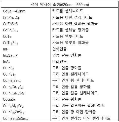
실시형태에서, 협대역 포토루미네선스 재료는 양자점(QD) 재료를 포함할 수 있다. 바람직한 실시형태에서, 양자점 재료는 카드뮴 셀레나이드(CdSe - FWHM ![]()
![]()
![]()
![]()
![]()
![]()
![]()
![]()
![]()
일부 실시형태에서, 발광 디바이스는 포토루미네선스 재료가 MQW 이중 파장 LED 상에 배치되는 패키지된 배열을 포함한다. 예를 들어, 포토루미네선스 재료는 표면 실장 디바이스(Surface Mount Device: SMD) 패키징 배열을 포함하지만 이에 한정되지 않는 LED를 포함하는 패키지에 배치될 수 있다. 대안적으로, 포토루미네선스 재료는 칩 스케일 패키지(Chip Scale Package: CSP) 배열로 개별 LED 다이 상에 직접 증착될 수 있다.In some embodiments, the light emitting device includes a packaged arrangement in which a photoluminescent material is disposed on an MQW dual wavelength LED. For example, the photoluminescent material may be disposed in a package containing an LED, including but not limited to a Surface Mount Device (SMD) packaging arrangement. Alternatively, the photoluminescent material may be deposited directly on individual LED dies in a Chip Scale Package (CSP) arrangement.
다른 실시형태에서, 발광 디바이스는 원격 포토루미네선스(예를 들어, 원격 형광체) 배열을 포함하며, 여기서 포토루미네선스 재료는 LED에 원격으로 위치된, 예를 들어 포토루미네선스 시트와 같은 포토루미네선스 층을 포함한다. 이 특허 명세서에서 "원격으로(Remotely)"는 간격을 두거나 분리된 관계를 의미한다. 분리는 에어 갭일 수 있거나, 또는 LED와 포토루미네선스 층/시트 사이에 광 투과성 매질을 포함할 수 있다. 이러한 원격 형광체 배열은 디스플레이 백라이트에서 특정 적용예를 찾을 수 있고, 포토루미네선스 층은 디스플레이의 층을 포함할 수 있다.In another embodiment, the light emitting device comprises a remote photoluminescence (eg, remote phosphor) arrangement, wherein the photoluminescence material is located remotely to the LED, such as a photoluminescence sheet, for example. and a photoluminescence layer. In this patent specification, "remotely" means a spaced apart or separated relationship. The separation may be an air gap, or may include a light transmissive medium between the LED and the photoluminescence layer/sheet. Such remote phosphor arrangements may find particular application in display backlights, where the photoluminescence layer may comprise a layer of a display.
다양한 실시형태에서, 포토루미네선스 재료는 광 투과성 매질에 분산될 수 있다. 광 투과 매질은 다이메틸 실리콘 또는 페닐 실리콘을 포함할 수 있다. 포토루미네선스 재료의 굴절률과 더 잘 일치시키기 위해, 사용되는 포토루미네선스 재료의 조성에 기초하여 페닐 실리콘(굴절률 ~1.54) 또는 다이메틸 실리콘(굴절률 1.41)이 선택될 수 있다. 예를 들어, K2SiF6:Mn4+(굴절률 ~1.4)는 다이메틸 실리콘에 분산되는 한편, K2TiF6:Mn4+(굴절률 >1.5)는 페닐 실리콘에 분산될 수 있다.In various embodiments, the photoluminescent material may be dispersed in a light transmissive medium. The light transmitting medium may include dimethyl silicone or phenyl silicone. In order to better match the refractive index of the photoluminescent material, phenyl silicon (refractive index ~1.54) or dimethyl silicon (refractive index 1.41) can be selected based on the composition of the photoluminescent material used. For example, K 2 SiF 6 :Mn 4+ (refractive index ~1.4) may be dispersed in dimethyl silicon, while K 2 TiF 6 :Mn 4+ (refractive index >1.5) may be dispersed in phenyl silicon.
본 발명의 발광 디바이스는 컬러 LCD용 백라이트와 관련하여 생겨났지만, MQW 이중 파장 LED 및 적색 포토루미네선스 재료를 포함하는 발광 디바이스는 또한 일반 조명 적용예에 유용성을 찾을 수 있다. 예를 들어, 일반 조명 적용예에서, MQW 이중 파장 LED는 500㎚ 내지 560㎚의 주파장 및 더 넓은 FWHM(Full Width at Half Maximum) 방출 강도, 예를 들어 약 15㎚ 내지 약 60㎚, 약 25㎚ 내지 약 60㎚, 또는 약 45㎚ 내지 약 60㎚를 갖는 청색 광 및/또는 녹색 광을 생성하도록 구성될 수 있다. 일반 조명 적용예에서, 예를 들어, 적색 포토루미네선스 재료는, 즉 가시 스펙트럼의 황색 내지 적색 영역에서, 600㎚ 내지 660㎚의 피크 방출 강도 파장을 가질 수 있다. 적색 포토루미네선스 재료는 일반 조성 CaAlSiN3:Eu(CASN) 또는 (Sr,Ca)AlSiN3:Eu(SCASN)의 칼슘 알루미늄 실리콘 질화물계 형광체와 같은 유로퓸 활성화된 질화물계 포토루미네선스 재료와 같은 광대역 적색 포토루미네선스 재료를 포함할 수 있다. 포토루미네선스 재료는 협대역 적색 포토루미네선스 재료를 추가로 포함할 수 있다. 발광 디바이스는 패키지된 배열, 예를 들어 SMD 패키징 배열, 칩 온 보드(Chip On Board: COB), LED 필라멘트 - 칩 온 글라스(Chip On Glass: COG), 및 칩 스케일 패키지(Chip Scale Package: CSP) 배열 또는 원격 형광체 배열을 포함할 수 있다.Although the light emitting devices of the present invention have arisen in the context of backlights for color LCDs, light emitting devices comprising MQW dual wavelength LEDs and red photoluminescent materials may also find utility in general lighting applications. For example, in general lighting applications, MQW dual wavelength LEDs have a dominant wavelength of 500 nm to 560 nm and a wider Full Width at Half Maximum (FWHM) emission intensity, such as about 15 nm to about 60 nm, about 25 nm. and may be configured to generate blue light and/or green light having from about 45 nm to about 60 nm, or from about 45 nm to about 60 nm. In general lighting applications, for example, a red photoluminescent material may have a peak emission intensity wavelength of 600 nm to 660 nm, ie in the yellow to red region of the visible spectrum. The red photoluminescent material may be a europium-activated nitride-based photoluminescent material such as a calcium aluminum silicon nitride-based phosphor of the general composition CaAlSiN 3 :Eu(CASN) or (Sr,Ca)AlSiN 3 :Eu(SCASN). broadband red photoluminescent material. The photoluminescent material may further comprise a narrowband red photoluminescent material. Light emitting devices are packaged arrays such as SMD packaging arrays, Chip On Board (COB), LED Filament-Chip On Glass (COG), and Chip Scale Package (CSP). arrays or remote phosphor arrays.
본 발명의 이들 및 다른 양태 및 특징은 첨부 도면과 함께 본 발명의 특정 실시형태에 대한 다음의 설명을 검토할 때 당업자에게 명백해질 것이며, 여기서:
도 1은 본 발명의 실시형태에 따른 패키지된 포토루미네선스 파장 변환된 백색 발광 디바이스의 측단면도이고;
도 2a, 도 2b 및 도 2c는 예시적인 다중 양자 우물(MQW) 이중 파장 LED 칩 구조의 개략도이고;
도 3a 및 도 3b는 각각 본 발명의 실시형태에 따른 칩 온 보드(COB) 패키지된 백색 발광 디바이스의 A-A를 통한 (a) 평면도 및 (b) 측단면도이고;
도 4는 플립칩 이중 파장 LED 다이를 사용하는 본 발명의 실시형태에 따른 칩 스케일 패키지(CSP) 백색 발광 디바이스의 개략도이고;
도 5는 래터럴칩(lateral-chip) 이중 파장 LED 다이를 사용하는 본 발명의 실시형태에 따른 칩 스케일 패키지(CSP) 백색 발광 디바이스의 개략도이고;
도 6은 버티컬칩(vertical-chip) 이중 파장 LED 다이를 사용하는 본 발명의 실시형태에 따른 칩 스케일 패키지(CSP) 백색 발광 디바이스의 개략도이고;
도 7a 및 도 7b는 각각 본 발명의 실시형태에 따른 칩 원격 포토루미네선스 백색 발광 디바이스의 B-B를 통한 (a) 평면도 및 (b) 측단면도이고;
도 8a 및 도 8b는 각각 (a) 본 발명의 실시형태에 따른 에지 조명(edge-lit) 액정 디스플레이 및 (b) 본 발명의 실시형태에 따른 디스플레이 백라이트의 측단면도이고;
도 9는 본 발명의 실시형태에 따른 직접 조명(direct-lit) 백라이트의 개략적인 단면도이고;
도 10은 본 발명의 실시형태에 따른 직접 조명 백라이트의 개략적인 단면도이고;
도 11은 본 발명의 실시형태에 따른 원격 형광체 필름을 사용하는 직접 조명 백라이트의 개략적인 단면도이고;
도 12는 일반 조성 K2SiF6:Mn4+의 망간 활성화된 헥사플루오로규산칼륨(potassium hexafluorosilicate) 형광체(KSF)의 방출 스펙트럼을 나타내고;
도 13은 S/Se(황/셀레늄)의 상이한 비율에 대한 CSS 형광체(CSS604, CSS615, CSS624, CSS632, 및 CSS641로 표시됨)의 정규화된 방출 스펙트럼을 나타내고;
도 14는 다중 양자 우물(MQW) 이중 파장 LED에 대한 측정된 방출 스펙트럼인 강도 대 파장이고;
도 15는 본 발명의 실시형태에 따른 패키지된 발광 디바이스(백라이트)에 대한 측정된 방출 스펙트럼인 강도 대 파장이다.These and other aspects and features of the invention will become apparent to those skilled in the art upon review of the following description of specific embodiments of the invention in conjunction with the accompanying drawings, wherein:
1 is a cross-sectional side view of a packaged photoluminescence wavelength converted white light emitting device in accordance with an embodiment of the present invention;
2A, 2B and 2C are schematic diagrams of an exemplary multiple quantum well (MQW) dual wavelength LED chip structure;
3A and 3B are (a) a top view and (b) a side cross-sectional view, respectively, through AA of a chip on board (COB) packaged white light emitting device in accordance with an embodiment of the present invention;
4 is a schematic diagram of a chip scale package (CSP) white light emitting device in accordance with an embodiment of the present invention using a flip chip dual wavelength LED die;
5 is a schematic diagram of a chip scale package (CSP) white light emitting device in accordance with an embodiment of the present invention using a lateral-chip dual wavelength LED die;
6 is a schematic diagram of a chip scale package (CSP) white light emitting device in accordance with an embodiment of the present invention using a vertical-chip dual wavelength LED die;
7A and 7B are (a) top and (b) side cross-sectional views, respectively, through BB of a chip remote photoluminescent white light emitting device in accordance with an embodiment of the present invention;
8A and 8B are cross-sectional side views, respectively, of (a) an edge-lit liquid crystal display according to an embodiment of the present invention and (b) a display backlight according to an embodiment of the present invention;
9 is a schematic cross-sectional view of a direct-lit backlight according to an embodiment of the present invention;
10 is a schematic cross-sectional view of a direct illuminating backlight according to an embodiment of the present invention;
11 is a schematic cross-sectional view of a direct illuminating backlight using a remote phosphor film in accordance with an embodiment of the present invention;
12 shows an emission spectrum of a manganese-activated potassium hexafluorosilicate phosphor (KSF) of general composition K 2 SiF 6 :Mn 4+ ;
13 shows the normalized emission spectra of CSS phosphors (denoted as CSS604, CSS615, CSS624, CSS632, and CSS641) for different ratios of S/Se (sulfur/selenium);
14 is a measured emission spectrum, intensity versus wavelength for a multiple quantum well (MQW) dual wavelength LED;
15 is a measured emission spectrum, intensity versus wavelength, for a packaged light emitting device (backlight) in accordance with an embodiment of the present invention.
이제, 당업자가 본 발명을 실시할 수 있도록 본 발명의 예시적인 예로서 제공되는 도면을 참조하여 본 발명의 실시형태가 상세히 설명될 것이다. 특히, 아래의 도면 및 예는 본 발명의 범위를 단일 실시형태로 한정하는 것을 의미하지 않지만, 설명되거나 예시된 요소의 일부 또는 전부의 교환을 통해 다른 실시형태가 가능하다. 또한, 본 발명의 특정 요소가 공지된 구성요소를 사용하여 부분적으로 또는 완전히 구현될 수 있는 경우, 본 발명의 이해에 필요한 이러한 공지된 구성요소의 해당 부분만이 설명될 것이고, 이러한 공지된 구성요소의 다른 부분에 대한 상세한 설명은 본 발명을 모호하게 하지 않기 위해 생략될 것이다. 본 명세서에서, 단일 구성요소를 나타내는 실시형태는 한정하는 것으로 간주되지 않아야 하며; 오히려, 본 발명은 본 명세서에서 달리 명시적으로 언급되지 않는 한, 복수의 동일한 구성요소를 포함하는 다른 실시형태를 포함하도록 의도되며, 그 반대의 경우도 마찬가지이다. 또한, 출원인은 이와 같이 명시적으로 제시되지 않는 한 명세서 또는 청구범위의 임의의 용어가 일반적이지 않거나 특별한 의미로 간주되는 것을 의도하지 않는다. 또한, 본 발명은 예시를 통해 본 명세서에 언급된 공지된 구성요소에 대한 현재와 미래의 공지 등가물을 포함한다. 본 명세서 전반에 걸쳐 도면 번호가 선행되는 유사한 참조 번호는 유사한(균등한) 부분을 표시하는 데 사용된다.DETAILED DESCRIPTION OF THE PREFERRED EMBODIMENTS Now, embodiments of the present invention will be described in detail with reference to the drawings, which are provided as illustrative examples of the present invention to enable those skilled in the art to practice the present invention. In particular, the drawings and examples below are not meant to limit the scope of the invention to a single embodiment, but other embodiments are possible through exchange of some or all of the elements described or illustrated. Further, to the extent that certain elements of the present invention can be partially or fully implemented using known components, only those portions of those known components necessary for an understanding of the present invention will be described, and these known components will be described. Detailed descriptions of other parts of the will be omitted so as not to obscure the present invention. In this specification, an embodiment representing a single component should not be considered limiting; Rather, the invention is intended to cover other embodiments comprising a plurality of identical elements, and vice versa, unless expressly stated otherwise herein. Furthermore, Applicants do not intend for any term in the specification or claims to be regarded as having an unusual or special meaning unless expressly set forth as such. Furthermore, the present invention includes present and future known equivalents to the known elements mentioned herein by way of illustration. Throughout this specification, like reference numbers preceded by reference numbers are used to denote like (equal to) parts.
본 발명의 실시형태는 청색 및 녹색 광 방출을 생성하는 MQW 이중 파장 LED를 포함하는 포토루미네선스 파장 변환된 발광 디바이스에 관한 것이다. 전술한 바와 같이, MQW 이중 파장 LED는 청색 및 녹색의 2개(이중)의 다른 색상(파장)의 광을 생성하는 단일 LED 다이(또는 칩)로서 정의된다.Embodiments of the present invention relate to photoluminescent wavelength converted light emitting devices comprising MQW dual wavelength LEDs that produce blue and green light emission. As noted above, an MQW dual wavelength LED is defined as a single LED die (or chip) that produces light in two (dual) different colors (wavelengths) of blue and green.
패키지된 백색 발광 디바이스/백라이트Packaged White Light Emitting Device/Backlight
이제 본 발명의 일 실시형태에 따른 패키지된 포토루미네선스 파장 변환된 백색 발광 디바이스(110)가 발광 디바이스(110)의 측단면도를 나타내는 도 1을 참조하여 설명될 것이다. 발광 디바이스(110)는, 예를 들어 표면 실장 디바이스(SMD) 2835 LED 패키지(리드 프레임)(112)를 포함하는 패키지형 디바이스이다. SMD 패키지(112)는 일반적으로 직사각형 베이스(114) 및 베이스(114)의 대향 에지로부터 상향으로 연장되는 측벽(116a, 116b)을 포함한다. 측벽(116a, 116b)의 내부 표면은 나타낸 바와 같이 수직 방향으로 베이스로부터 외측으로 경사지고 베이스(114)의 내부 표면과 함께 피라미드의 역 절두체(inverted frustum) 형태의 공동(118)을 획정한다.A packaged photoluminescence wavelength converted white
이 실시형태에서, 공동(118)은 하나 이상의 이중 파장 LED 다이(120)(도 1에는 하나만 도시됨) 및 공동(118)을 채우는 적색 발광 포토루미네선스 재료를 포함하는 포토루미네선스 층(122)을 포함한다. 적색 포토루미네선스 재료는 620㎚ 내지 660㎚ 범위의 피크 방출 파장(λpe)을 갖는 적색 광을 생성하도록 작동 가능하다.In this embodiment, the
LED 다이(120)는 공동(118)의 바닥에 있는 각각의 본딩 패드(124) 상에 장착된다. 상기 또는 각 LED 다이(120)는 그 상부 표면의 대향 단부 상에 n-전극(126a) 및 p-전극(126b)을 포함한다. 본드 와이어(128a, 128b)는 n-전극(126a) 및 p-전극(126b)을, 공동(118)의 바닥에 장착되는 대응하는 접촉 패드(130a, 130b)에 연결한다. 접촉 패드(130a, 130b)는 베이스(114)의 하면 상에서 외부 접촉 패드(132a, 132b)에 전기적으로 연결된다.An LED die 120 is mounted on each
포토루미네선스 층(122)은, 통상적으로 예를 들어 실리콘 재료와 같은 광 투과성 광학 캡슐화제(매질)에 분산되는 입자 형태의 형광체 재료로 구성될 수 있다. 포토루미네선스 층(122)은 도시된 바와 같이 LED 다이(120)와 접촉할 수 있고, 나타낸 바와 같이 공동(118)을 채울 수 있다. 디바이스 적용예에 따라, 포토루미네선스 재료는 디바이스 적용예에 따라 광대역(약 25㎚ 내지 약 60㎚의 FWHM 방출 강도) 또는 협대역(약 5㎚ 내지 약 25㎚의 FWHM 방출 강도) 재료일 수 있다. 광대역 및 협대역 적색 포토루미네선스 재료의 예가 후술된다.The
MQW 이중 파장 LEDMQW Dual Wavelength LED
본 발명에 따르면, MQW 이중 파장 LED 다이(120)는, a) 작동 시 440㎚ 내지 470㎚의 주파장(λd1)을 갖는 청색 광을 생성하는 하나 이상의 제1 양자 우물(QW) 및 b) 작동 시 520㎚ 내지 540㎚의 주파장(λd2)을 갖는 녹색 광을 생성하는 하나 이상의 제2 QW를 포함하는 InGaN/GaN(인듐 갈륨 질화물/갈륨 질화물) MQW 이중 파장 LED 다이를 포함할 수 있다. 통상적으로, MQW 이중 파장 LED는 복수의 제1 및 제2 양자 우물을 포함할 것이고; 즉, 제1 및 제2 QW 자체는 각각의 MQW 구조를 각각 포함한다.In accordance with the present invention, the MQW dual wavelength LED die 120 comprises: a) one or more first quantum wells QW that, when operated, produce blue light having a dominant wavelength λ d1 between 440 nm and 470 nm and b) an InGaN/GaN (indium gallium nitride/gallium nitride) MQW dual wavelength LED die comprising one or more second QWs that when operated produce green light having a dominant wavelength (λ d2 ) between 520 nm and 540 nm . Typically, an MQW dual wavelength LED will include a plurality of first and second quantum wells; That is, the first and second QWs themselves each include respective MQW structures.
도 2a, 도 2b 및 도 2c는 본 발명에서 사용될 수 있는 예시적인 MQW 이중 파장 LED 구조의 개략도이다. 본 발명에 사용하기에 적합한 다른 적합한 MQW LED 구조가 존재함을 이해할 것이다. 도 2a 및 도 2b는 단일 칩으로서 제조된 각각의 청색 및 녹색 MQW LED 구조를 본질적으로 포함하는 모놀리식 디바이스라고 지칭될 수 있는 한편, 도 2c는 청색 및 녹색 광을 생성할 수 있는 단일 MQW LED 구조를 포함한다.2A, 2B and 2C are schematic diagrams of exemplary MQW dual wavelength LED structures that may be used in the present invention. It will be appreciated that other suitable MQW LED structures suitable for use in the present invention exist. 2A and 2B may be referred to as a monolithic device essentially comprising respective blue and green MQW LED structures fabricated as a single chip, while FIG. 2C is a single MQW LED capable of producing blue and green light. include structure.
도 2a를 참조하면, LED 칩(220)은, 사파이어 기판(220a), 제1 n-도핑 GaN(n-GaN) 층(220b), 주파장(λd2)의 녹색 광을 생성하기 위한 제2 InGaN MQW 구조 층(220c), 제1 p-도핑 GaN(p-GaN)층(220d), 배리어 층(220e), 제2 n-도핑 GaN(n-GaN) 층(220f), 주파장(λd1)의 청색 광을 생성하기 위한 제1 InGaN MQW 구조 층(220g) 및 제2 p-도핑 GaN(p-GaN) 층(220h)을 순서대로 포함하는 층 구조를 포함한다. n-전극(226a) 및 p-전극(226b)은 각각 제1 n-GaN 층(220b) 및 제2 p-GaN 층(220h)에 전기적으로 연결된다. MQW 구조(220c, 220g)에 의해 생성된 광의 주파장(λd)은 QW의 인듐(In) 도핑, QW 층 폭과 수, 및 QW의 주파장(λd) 간격에 의존할 수 있다. 층(220b 내지 220d)을 포함하는 구조는 녹색 광을 생성하는 각각의 녹색 MQW LED 구조(p-n 접합 다이오드)를 구성하는 한편, 층(220f 내지 220h)을 포함하는 구조는 청색 광을 생성하는 각각의 청색 MQW LED 구조를 구성한다는 것이 이해될 것이다. 녹색 및 청색 MQW LED 구조는 직렬로 전기 연결된다. 적용예에 따라, 청색(제1) 및 녹색(제2) QW의 수 및 주파장(λd) 간격은 약 15㎚ 내지 약 45㎚의 FWHM 방출 강도를 갖는 청색 광 및/또는 녹색 광을 생성하도록 구성될 수 있다. 예를 들어, 일반 조명 적용예에서, 청색 및/또는 녹색 광은 일반적으로, 예를 들어 약 25㎚ 내지 약 645㎚의 더 넓은 FWHM 방출 강도를 가질 것이다. 디스플레이 백라이트 적용예에서, 청색 광 및/또는 녹색 광은 일반적으로, 예를 들어 약 15㎚ 내지 약 25㎚의 더 좁은 FWHM 방출 강도를 가질 것이다.Referring to FIG. 2A , the
도 2a의 배열에서, 청색(제1) 및 녹색(제2) MQW 층(220g, 220c)은 수직 배열로 서로 적층된다. 다른 실시형태에서, 청색 및 녹색 QW는 단일 층 내에 측방향으로 위치될 수 있다. 도 2b를 참조하면, LED 칩(220)은, 사파이어 기판(220a), n-도핑 GaN(n-GaN) 층(220b), 주파장(λd1)의 청색 광과 주파장(λd2)의 녹색 광을 각각 생성하기 위한 제1 및 제2 InGaN MQW 구조(220g, 220c) 및 p-도핑 GaN(p-GaN) 층(220h)을 순서대로 포함하는 층 구조를 포함한다. 도 2b에 나타낸 바와 같이, 제1 및 제2 MQW 구조(220g, 220c)는 단일 층에 측방향으로 위치되며, 배리어 층(220e)에 의해 분리될 수 있다. n-전극(126a) 및 p-전극(126b)은 각각 n-GaN 층(220b) 및 p-GaN 층(220h)에 전기적으로 연결된다. 층(220b, 220g, 220h)을 포함하는 구조는 청색 광을 생성하는 각각의 청색 MQW LED 구조(p-n 접합 다이오드)를 구성하는 한편, 층(220b, 220c, 220h)을 포함하는 구조는 녹색 광을 생성하는 각각의 녹색 MQW LED 구조를 구성한다는 것이 이해될 것이다. 청색 및 녹색 MQW LED 구조는 병렬로 전기 연결된다. 청색 및 녹색 MQW 구조에 의해 생성된 광의 주파장(λd)은 인듐(In) 도핑, QW 층 폭과 수, 및 QW의 주파장(λd) 간격에 의존할 수 있다. 적용예에 따라, 청색(제1) 및 녹색(제2) QW의 수 및 주파장(λd) 간격은 약 15㎚ 내지 약 45㎚의 FWHM 방출 강도를 갖는 청색 광 및/또는 녹색 광을 생성하도록 구성될 수 있다. 예를 들어, 일반 조명 적용예에서, 청색 및/또는 녹색 광은 일반적으로, 예를 들어 약 25㎚ 내지 약 45㎚의 더 넓은 FWHM 방출 강도를 가질 것이다. 디스플레이 백라이트 적용예에서, 청색 광 및/또는 녹색 광은 일반적으로, 예를 들어 약 15㎚ 내지 약 25㎚의 더 좁은 FWHM 방출 강도를 가질 것이다.In the arrangement of FIG. 2A , blue (first) and green (second) MQW layers 220g, 220c are stacked on top of each other in a vertical arrangement. In other embodiments, the blue and green QWs may be laterally located within a single layer. Referring to FIG. 2b , the
도 2c는 청색 광과 녹색 광 모두를 생성할 수 있는 단일 MQW LED 구조의 개략도이다. 도 2c를 참조하면, LED 칩(220)은, 사파이어 기판(220a), n-도핑 GaN(n-GaN) 층(220b), 주파장(λd2)의 녹색 광을 생성하기 위한 제2 InGaN MQW 구조 층(220c), 주파장(λd1)의 청색 광을 생성하기 위한 제1 InGaN MQW 구조 층(220g) 및 a-도핑 GaN(p-GaN) 층(220h)을 순서대로 포함하는 층 구조를 포함한다. n-전극(226a) 및 p-전극(226b)은 각각 n-GaN 층(220b) 및 p-GaN 층(220h)에 전기적으로 연결된다. 청색 및 녹색 MQW 구조에 의해 생성된 광의 주파장(λd)은 QW의 인듐(In) 도핑, QW 층 폭과 수, 및 QW의 주파장(λd) 간격에 의존할 수 있다. 층(220b, 220c, 220g, 220h)을 포함하는 구조는 청색 광과 녹색 광 모두를 생성하는 단일 MQW LED 구조(p-n 접합 다이오드)를 구성한다는 것이 이해될 것이다. 적용예에 따라, 청색(제1) 및 녹색(제2) QW의 수 및 주파장(λd) 간격은 약 15㎚ 내지 약 60㎚의 FWHM 방출 강도를 갖는 청색 광 및/또는 녹색 광을 생성하도록 구성될 수 있다. 예를 들어, 일반 조명 적용예에서, 청색 및/또는 녹색 광은 일반적으로, 예를 들어 약 25㎚ 내지 약 60㎚의 더 넓은 FWHM 방출 강도를 가질 것이다. 디스플레이 백라이트 적용예에서, 청색 광 및/또는 녹색 광은 일반적으로, 예를 들어 약 15㎚ 내지 약 25㎚의 더 좁은 FWHM 방출 강도를 가질 것이다. 도시된 바와 같이, 녹색(제2) MQW 구조(220c)는 n-GaN 층(220b)에 인접하게 배치될 수 있고, 청색(제1) InGaN MQW 구조 층(220g)은 청색 InGaN 구조 층(220g)의 상부에 배치되고 p-GaN 층(220h)에 인접하게 위치될 수 있다. 다른 구성에서, 청색 및 녹색 MQW 구조 층의 위치는 n-GaN 층(220b)에 인접하게 위치된 청색(제1) MQW 구조(220g) 및 p-GaN 층(220h)에 인접하게 위치된 녹색(제2) MQW 구조 층(220c)으로 전치될 수 있다. 또한, MQW 구조 층(220c 및 220g)이 서로 적층된 각각의 MQW 구조를 포함하는 것으로 도시되어 있지만, 제1 및 제2 MQW는 단일 구조, 예를 들어 개재된(예를 들어, 교번하는) 청색 및 녹색 QW의 스택을 포함하는 단일 MQW 구조 층으로서 통합될 수 있다.2C is a schematic diagram of a single MQW LED structure capable of generating both blue and green light. Referring to FIG. 2C , the
도 1을 참조하면, 작동 시, 이중 파장 LED 다이(120)로부터의 청색 광의 부분은 포토루미네선스 층(122) 내의 포토루미네선스 재료에 의해 적색 광으로 변환된다. 이중 파장 LED 다이(들)(120)에 의해 생성된 녹색 광, 포토루미네선스 재료에 의해 생성된 적색 광 및 이중 파장 LED 다이(들)에 의해 생성된 변환되지 않은 청색 광의 조합은 백색 발광 생성물을 생성한다. 포토루미네선스 재료의 여기 스펙트럼(특성)에 따라, 이중 파장 LED 다이에 의해 생성된 녹색 광의 부분이 또한 포토루미네선스 재료에 의해 적색 광으로 변환될 수 있다.Referring to FIG. 1 , in operation, a portion of the blue light from the dual wavelength LED die 120 is converted to red light by the photoluminescence material in the
이제 본 발명의 일 실시형태(310)에 따른 COB(Chip On Board) 패키지된 백색 발광 디바이스(310)가 도 3a 및 도 3b를 참조하여 설명될 것이다. 디바이스(310)는 기판(314) 상에 배치된 다수(12개)의 MQW 이중 파장 LED 다이(320), 및 LED 다이(320) 위에 배치된 포토루미네선스 재료(322)를 포함한다. 보다 구체적으로, 도 3a는 COB 백색 발광 디바이스(310)의 평면도를 나타내고, 도 3b는 (도 3a의) A-A를 통한 측단면도를 나타낸다. 기판(314)은 평면이고 정사각형이며, 금속 코어 인쇄 회로 기판(MCPCB)일 수 있다. 12개의 이중 파장 LED 다이(320)는 원형 어레이의 형태로 기판(314) 상에 균일하게 분포된다. 디바이스(310)는 기판(314)의 전체 둘레에 대해, LED 다이(320)의 어레이를 둘러싸고 기판(314)의 표면과 함께 원형 공동(318)을 획정하는 환형 벽(316)을 포함한다. LED 다이(320)는 440㎚ 내지 470㎚의 주파장(λd1)을 갖는 청색 광 및 520㎚ 내지 540㎚의 주파장(λd2)을 갖는 녹색 광을 생성하도록 작동 가능하다.A Chip On Board (COB) packaged white
적색 포토루미네선스 재료(322)는 LED 다이(320)를 완전히 덮고 공동(318)을 채우기 위해 벽(316) 내부의 기판(314) 상에 증착된다. 적색 포토루미네선스 재료(322)는 620㎚ 내지 660㎚의 피크 방출 파장(λpe)을 갖는 적색 광을 생성하도록 작동 가능하다.A
작동 시, LED 다이(320)에 의해 생성된 청색 광의 부분은 포토루미네선스 재료에 의해 적색 광으로 변환된다. LED 다이(320)에 의해 생성된 녹색 광, 포토루미네선스 재료에 의해 생성된 적색 광 및 LED 다이에 의해 생성된 변환되지 않은 청색 광의 조합은 백색 발광 생성물을 생성한다.In operation, a portion of the blue light generated by the LED die 320 is converted to red light by the photoluminescent material. The combination of the green light produced by the LED die 320, the red light produced by the photoluminescent material, and the unconverted blue light produced by the LED die produces a white light emitting product.
선택적으로, 백색 발광 디바이스(310)는 확산 층(334)(도 3b에 파선으로 표시됨)을 포함할 수 있다. 확산 층은 백색 발광 디바이스(310)에 의한 발광의 색 균일성을 개선할 수 있다. 확산 층은 포토루미네선스 재료(322)와 직접 접촉할 수 있다. 확산 층은 광 투과성 재료 및 광 산란 입자를 포함할 수 있다. 향상된 색 균일성은 디바이스가 대형 빔 광학 기기에 사용될 때 특히 유리할 수 있다. 광 산란 입자를 포함하는 확산 층은 청색 여기 광을 포토루미네선스 재료(322) 내로 다시 유도함으로써 광자가 포토루미네선스 광의 생성을 초래할 확률을 증가시킨다. 따라서, 더 많은 청색 여기 광이 확산 층에 의해 포토루미네선스 광으로 변환되기 때문에 광의 주어진 색 온도를 생성하는 데 필요한 포토루미네선스 재료의 양이 감소될 수 있다. 또한, 포토루미네선스 재료의 양을 감소시키는 것은 특히 KSF와 같은 고가의 망간 활성화된 불화물 형광체를 사용할 때 백색 발광 디바이스(310)를 제조하는 보다 비용 효율적인 방식을 제공한다.Optionally, the white
이제 도 4를 참조하면, 플립칩 LED 다이(420)를 사용하는 본 발명의 실시형태에 따른 칩 스케일 패키지(CSP) 백색 발광 디바이스의 개략도가 도시되어 있다.Referring now to FIG. 4 , there is shown a schematic diagram of a chip scale package (CSP) white light emitting device in accordance with an embodiment of the present invention using a flip chip LED die 420 .
CSP 백색 발광 디바이스(410)는 각각의 발광 면(통상적으로 상부 및 4개의 측면) 상에 적색 포토루미네선스 재료 코팅층(422)을 갖는 MQW 이중 파장 LED 플립칩 LED 다이(420)를 포함한다. LED 다이(422)는 440㎚ 내지 470㎚의 주파장(λd1)을 갖는 청색 광 및 520㎚ 내지 540㎚의 주파장(λd2)을 갖는 녹색 광을 생성하도록 작동 가능하다. 적색 포토루미네선스 재료(422)는 620㎚ 내지 640㎚의 피크 방출 파장(λpe)을 갖는 적색 광을 생성한다. LED 다이(420)는 베이스(436)에 n-전극(426a) 및 p-전극(426b)을 포함한다. n-전극(426a) 및 p-전극(426b)은 플립칩 본딩(434a, 434b)에 의해 2개의 대응하는 본딩 패드(430a, 430b)에 전기적으로 연결된다. 접촉 패드(430a, 430b)는 평면 기판(414) 상에 장착된다.The CSP white
도 5를 참조하면, 래터럴칩 이중 파장 LED 다이(520)를 사용하는 본 발명의 실시형태에 따른 CSP 백색 발광 디바이스의 개략도가 도시되어 있다.Referring to FIG. 5 , a schematic diagram of a CSP white light emitting device in accordance with an embodiment of the present invention using a lateral chip dual wavelength LED die 520 is shown.
발광 디바이스(510)는 상부(538b) 및 모든 측면(538a, 538c) 상에 적색 포토루미네선스 재료(522)로 코팅된 MQW 이중 파장 LED 다이(520)를 포함한다. LED 다이(520)는 베이스(536) 상에 본딩 패드(524)를 갖는다. LED 다이(520)는 MQW 구조를 포함하고, 440㎚ 내지 470㎚의 주파장(λd1)을 갖는 청색 광 및 520㎚ 내지 540㎚의 주파장(λd2)을 갖는 녹색 광을 생성하도록 작동 가능하다. 적색 포토루미네선스 재료(522)는 620㎚ 내지 640㎚의 피크 방출 파장(λpe)을 갖는 적색 광을 생성한다. LED 다이(520)는 그 상부 표면(538b)의 대향 단부 상에 n-전극(526a) 및 p-전극(526b)을 포함한다. 본드 와이어(528a, 528b)는 n-전극(524a) 및 p-전극(524b)을, 평면 기판(514) 상에 장착되는 대응하는 접촉 패드(530a, 530b)에 연결한다.
도 6을 참조하면, 버티컬칩 이중 파장 LED 다이(620)를 사용하는 본 발명의 실시형태에 따른 CSP 백색 발광 디바이스의 개략도가 도시되어 있다.Referring to FIG. 6 , a schematic diagram of a CSP white light emitting device in accordance with an embodiment of the present invention using a vertical chip dual wavelength LED die 620 is shown.
발광 디바이스(610)는 상부 표면(638b)에만 적색 포토루미네선스 재료(들)(622)로 코팅된 MQW 이중 파장 LED 버티컬칩 LED 다이(620)를 포함한다. 보다 구체적으로, 버티컬칩이 상부 표면으로부터만 광을 방출하기 때문에 측면(638a, 638c)은 포토루미네선스 재료(들)로 코팅되지 않는다. LED 다이(620)는 MQW 구조를 포함하고, 440㎚ 내지 470㎚의 주파장(λd1)을 갖는 청색 광 및 520㎚ 내지 540㎚의 주파장(λd2)을 갖는 녹색 광을 생성하도록 작동 가능하다. 다이(620)는 본딩 패드(632) 상에 안착되는 베이스(626)에 n-전극(626a)을 포함한다. 결국, 본딩 패드(632)는 평면 기판(614) 상에 장착되는 접촉 패드(630a) 상에 안착된다. LED 다이(620)는 그 상부 표면의 일단부(638b) 상에 p-전극(624b)을 포함한다. 본드 와이어(624)는 p-전극(624b)을, 평면 기판(614) 상에 장착되는 대응하는 접촉 패드(630b)에 연결한다. 적색 포토루미네선스 재료(622)는 620㎚ 내지 660㎚의 피크 방출 파장(λpe)을 갖는 적색 광을 생성하도록 작동 가능하다.
원격 포토루미네선스 백색 발광 디바이스Remote photoluminescence white light emitting device
패키지된 백색 발광 디바이스뿐만 아니라, 본 발명은 또한 포토루미네선스 재료가 LED 다이에 원격으로 위치된 포토루미네선스 층을 포함하는 원격 포토루미네선스(예를 들어, 원격 형광체) 배열에서 유용성을 찾는다. 이 특허 명세서에서 "원격으로(Remotely)"는 간격을 두거나 분리된 관계를 의미한다. 분리는 에어 갭에 의한 것일 수 있거나, 또는 LED 다이와 포토루미네선스 층 사이에 광 투과성 매질을 포함할 수 있다.In addition to packaged white light emitting devices, the present invention also finds utility in remote photoluminescence (eg, remote phosphor) arrangements wherein the photoluminescence material includes a photoluminescence layer remotely located on an LED die. look for In this patent specification, "remotely" means a spaced apart or separated relationship. Separation may be by an air gap, or may include a light transmissive medium between the LED die and the photoluminescence layer.
이제 본 발명의 실시형태에 따른 원격 포토루미네선스 파장 변환된 백색 발광 디바이스 배열(710)이 도 7a 및 도 7b를 참조하여 설명될 것이다. 보다 구체적으로, 도 7a는 원격 포토루미네선스 백색 발광 디바이스(710)의 부분 단면 평면도를 나타내고, 도 7b는 (도 7a의) B-B를 통한 측단면도를 나타낸다.A remote photoluminescence wavelength converted white light emitting
디바이스는(710)는 단독으로 사용되거나 다운라이트 또는 기타 조명 배열의 일부를 포함할 수 있다. 디바이스(710)는 원형 디스크 형상의 베이스(742), 중공의 원통형 벽 부분(744) 및 탈착 가능한 환형 상부(746)로 구성된 중공의 원통형 본체(740)를 포함한다. 열 발산을 돕기 위해, 베이스(742)는 알루미늄, 알루미늄 합금 또는 높은 열전도율을 갖는 임의의 재료로 제조될 수 있다.
디바이스는(710)는 원형의 MCPCB(금속 코어 인쇄 회로 기판)(748)와 열 연통하도록 장착되는 다수(도 1a 및 도 1b의 예에서는 5개)의 패키지된 MQW 이중 파장 LED(720)를 더 포함한다. 광의 방출을 최대화하기 위해, 디바이스(710)는 MCPCB(748)의 면 및 원통형 벽(744)의 내부 곡면을 각각 덮는 광 반사 표면(750, 752)을 더 포함할 수 있다. LED 다이(720) 각각은 MQW 구조를 포함하며, 440㎚ 내지 470㎚의 주파장(λd1)을 갖는 청색 광 및 520㎚ 내지 540㎚의 주파장을 갖는 녹색 광을 생성하도록 작동 가능하다.
디바이스(710)는, LED(720)에 원격으로 위치되어 LED(720)에 의해 생성된 청색/녹색 여기 광의 일부를 흡수하고 이를 포토루미네선스의 프로세스에 의해 다른 파장의 광으로 변환하도록 작동 가능한 적색 포토루미네선스 재료를 포함하는 포토루미네선스 파장 변환 구성요소(722)를 더 포함한다. 적색 포토루미네선스 재료(722)는 620㎚ 내지 640㎚의 피크 방출 파장(λpe)을 갖는 적색 광을 생성하도록 작동 가능하다. 디바이스(710)의 방출 생성물은 LED(720)에 의해 생성된 청색 및 녹색 광과 포토루미네선스 파장 변환 구성요소(722)에 의해 생성된 포토루미네선스 광의 조합을 포함한다. 포토루미네선스 파장 변환 구성요소는 적색 포토루미네선스 재료(722)를 포함하는 광 투과성 재료(예를 들어, 폴리카보네이트, 아크릴 재료, 실리콘 재료 등)로 형성될 수 있다. 또한, 실시형태에서, 포토루미네선스 파장 변환 구성요소는 적색 포토루미네선스 재료로 코팅되는 광 투과성 기판으로 형성될 수 있다. 파장 변환 구성요소(722)는 LED(720)에 원격으로 위치되고 여기 소스로부터 공간적으로 분리된다. 이 특허 명세서에서, "원격으로(Remotely)" 및 "원격(remote)"은 간격을 두거나 분리된 관계를 의미한다. 통상적으로, 파장 변환 구성요소 및 여기 소스는 공기에 의해 분리되는 한편, 다른 실시형태에서는 예를 들어 광 투과성 실리콘 또는 에폭시 재료와 같은 적합한 광 투과성 매질에 의해 분리될 수 있다. 파장 변환 구성요소(722)는 디바이스에 의해 방출된 모든 광이 파장 변환 구성요소(722)를 통과하도록 하우징 개구를 완전히 덮도록 구성된다. 나타낸 바와 같이, 파장 변환 구성요소(722)는 상부(748)를 사용하여 벽 부분(744)의 상부에 탈착 가능하게 장착될 수 있어 램프의 구성요소 및 방출 색상이 쉽게 변경될 수 있게 한다.
액정 디스플레이 및 디스플레이 백라이트Liquid crystal displays and display backlights
전술한 백색 발광 디바이스가 일반 조명 적용예와 관련하여 설명될 수 있었지만, 본 발명의 실시형태에 따른 디바이스는 액정 디스플레이용 백라이트로서 유용성을 찾는다. 전술한 바와 같이, 백라이트 적용예의 경우, MQW LED 다이는, 예를 들어 약 15㎚ 내지 약 30㎚ 또는 약 15㎚ 내지 약 25㎚의 더 좁은 FWHM 방출 강도를 갖는 청색 광 및/또는 녹색 광을 생성하도록 구성된다. 마찬가지로, 적색 포토루미네선스 재료는 협대역 재료(약 10㎚ 내지 약 30㎚ 또는 약 15㎚ 내지 약 25㎚의 FWHM 방출 강도)를 포함할 수 있다.Although the white light emitting device described above could be described in the context of general lighting applications, a device according to an embodiment of the present invention finds utility as a backlight for liquid crystal displays. As noted above, for backlight applications, the MQW LED die produces blue light and/or green light having a narrower FWHM emission intensity of, for example, from about 15 nm to about 30 nm or from about 15 nm to about 25 nm. is configured to Likewise, the red photoluminescent material may include a narrowband material (FWHM emission intensity between about 10 nm and about 30 nm or between about 15 nm and about 25 nm).
도 8a 및 도 8b는 각각 (a) 광 투과성 에지 조명 컬러 액정 디스플레이(LCD)(860)의 단면도 및 (b) 본 발명의 실시형태에 따른 디스플레이 백라이트의 확대 단면도를 나타낸다. 컬러 LCD(860)는 LC(액정) 디스플레이 패널(862) 및 디스플레이 백라이트(864)를 포함한다. 백라이트(864)는 LC 디스플레이 패널(862)을 작동하기 위한 백색 광을 생성하도록 작동 가능하다.8A and 8B show, respectively, (a) a cross-sectional view of a light transmissive edge illuminated color liquid crystal display (LCD) 860 and (b) an enlarged cross-sectional view of a display backlight in accordance with an embodiment of the present invention. The
LC 디스플레이 패널(862)은 투명한(광 투과성) 전면(광/이미지 방출) 플레이트(866), 투명한 후면 플레이트(868) 및 전면 및 후면 플레이트(866, 868) 사이의 체적을 채우는 액정(LC)(870)을 포함한다.
전면 플레이트(866)는 상부 표면, 즉 디스플레이의 관찰 면(viewing face)을 포함하는 플레이트의 면 상에 제1 편광 필터 층(시트)(874)을 갖는 유리 플레이트(872)를 포함할 수 있다. 선택적으로, 전면 플레이트의 최외측 관찰 면은 반사 방지 층(876)을 더 포함할 수 있다. 그 하면, 즉 액정(LC)(870)을 향하는 전면 플레이트(866)의 면 상에서, 유리 플레이트(872)는 컬러 필터 플레이트(878) 및 광 투과성 공통 전극 평면(880)(예를 들어, 투명한 인듐 주석 산화물, ITO)을 더 포함할 수 있다.The
컬러 필터 플레이트(878)는 적색(R), 녹색(G) 및 청색(B) 광의 투과를 각각 허용하는 상이한 컬러 서브픽셀 필터 요소(R, G, B)의 어레이를 포함한다. 디스플레이의 각 단위 픽셀은 3개의 서브픽셀 필터 요소(R, G, B)의 그룹을 포함한다. 각 RGB 서브픽셀은, 서브픽셀의 색상에만 대응하는 광의 통과를 허용하는 각각의 컬러 필터 안료, 통상적으로 유기 염료를 포함한다.The
배면 플레이트(868)는 그 상부 표면(LC를 향하는 표면) 상에 TFT(Thin Film Transistor) 층(884)을 갖는 유리 플레이트(882)를 포함할 수 있다. TFT 층(884)은, 각 단위 픽셀의 각각의 개별 컬러 서브픽셀(R, G, B)에 대응하는 트랜지스터가 있는 TFT의 어레이를 포함한다. 각 TFT는 대응하는 서브픽셀로의 광의 통과를 선택적으로 제어하도록 작동 가능하다. 유리 플레이트(882)의 하부 표면 상에는 제2 편광 필터 층(시트)(886)이 제공된다. 2개의 편광 필터(874, 886)의 편광 방향은 서로 직교(수직) 정렬된다.The
백라이트(864)는 LC 디스플레이 패널(862)을 작동시키기 위해 전면 발광면(디스플레이 패널의 배면을 향하는 상부면)으로부터 백색 광을 생성 및 방출하도록 작동 가능하다. 도 8b에 나타낸 바와 같이, 백라이트(864)는 도광체(도파관)(888)를 포함하는 에지 조명 배열을 포함할 수 있고, 하나 이상의 패키지된 MQW 이중 파장 LED(820)가 도광체(888)의 하나 이상의 에지를 따라 위치된다. 각 MQW LED(820)는 440㎚ 내지 470㎚의 주파장(λd1)을 갖는 청색 광 및 500㎚ 내지 540㎚의 주파장을 갖는 녹색 광을 생성하도록 작동 가능하다. 나타낸 바와 같이, 도광체(888)는 평면일 수 있고; 그러나, 일부 실시형태에서는 도광체의 전면 발광면(디스플레이 패널을 향하는 상부면)으로부터 여기 광의 보다 균일한 방출을 촉진하기 위해 테이퍼형(쐐기형)일 수 있다. LED(820)는, 작동 시 청색/녹색 여기 광(890)을 생성하도록 구성되어 있으며, 청색/녹색 여기 광은 도광체(888)의 하나 이상의 에지에 결합된 다음, 내부 전반사에 의해, 도광체의 체적을 통해 안내되고 최종적으로 도광체(888)의 전면(디스플레이 패널(862)을 향하는 상부면)으로부터 방출된다. 도 8b에 나타낸 바와 같이, 그리고 백라이트(864)로부터의 광의 탈출을 방지하기 위해, 도광체(888)의 배면(나타낸 바와 같은 하부면)은 3M™으로부터의 Vikuiti™ ESR(Enhanced Spectral Reflector) 필름과 같은 광 반사 층(표면)(892)을 포함할 수 있다.The
도광체(888)의 전면 발광면(나타낸 바와 같은 상부면)에는 포토루미네선스 파장 변환 층(822) 및 휘도 향상 필름(Brightness Enhancement Film: BEF)(894)이 제공된다. 실시형태에서, 포토루미네선스 층은, 예를 들어 BEF(894) 또는 도광체(888) 상에 증착되는 별개의 시트/필름 또는 층을 포함할 수 있다. 본 발명의 실시형태에 따르면, 포토루미네선스 층은 620㎚ 내지 640㎚의 피크 방출 파장(λpe)을 갖는 적색 광을 생성하는 적색 포토루미네선스 재료를 포함한다. 포토루미네선스 재료가 LED(820)로부터 분리되고 떨어져 있는 별도의 개별 층(822)에 제공되기 때문에, 백라이트는 여기 소스 및 포토루미네선스 재료가 광학 매질(도광체(888))에 의해 분리되어 있는 원격 포토루미네선스 배열을 구성한다는 것이 이해될 것이다. 작동 시, 포토루미네선스 층(822)은 청색 여기 광(포토루미네선스 재료의 여기 스펙트럼에 따라 녹색 광일 수도 있음)의 부분을 LC 디스플레이 패널(862)을 작동시키기 위한 백색 광(898)으로 변환한다. 디스플레이의 효율 및 색 영역을 최적화하기 위해, 청색 광의 주파장(λd1) 및 녹색 광의 주파장(λd2) 및 적색 포토루미네선스 재료의 피크 방출 파장(λpe)은 대응하는 컬러 필터 요소(RGB)의 최대 투과 특성과 실질적으로 대응하도록 선택된다.The top emitting surface (top surface as shown) of the
프리즘 시트라고도 알려진 휘도 향상 필름(BEF)은 정밀한 마이크로 구조의 광학 필름을 포함하고, 고정된 각도(일반적으로 70도) 내에서 백라이트로부터의 광의 방출을 제어하여, 백라이트의 발광 효율을 증가시킨다. 통상적으로, BEF는 필름의 발광면 상에 마이크로 프리즘의 어레이를 포함하며, 휘도를 40-60% 만큼 증가시킬 수 있다. BEF(894)는 단일 BEF 또는 다수의 BEF의 조합을 포함할 수 있으며, 후자의 경우에는 훨씬 더 큰 휘도 증가가 달성될 수 있다. 적합한 BEF의 예는 3M™으로부터의 Vikuiti™ BEF II 또는 MNTech로부터의 프리즘 시트를 포함한다. 일부 실시형태에서, BEF(894)는, 프리즘 시트를 확산 필름과 통합하며 일반 프리즘 시트보다 더 나은 발광 효율을 가질 수 있는 다기능 프리즘 시트(Multi-Functional Prism Sheet: MFPS)를 포함할 수 있다. 일부 실시형태에서, BEF(894)는 MNTech로부터 입수 가능한 것과 같은 마이크로 렌즈 필름 프리즘 시트(Micro-Lens Film Prism Sheet: MLFPS)를 포함할 수 있다.A brightness enhancing film (BEF), also known as a prism sheet, contains an optical film with a precise microstructure, and controls the emission of light from the backlight within a fixed angle (typically 70 degrees), thereby increasing the luminous efficiency of the backlight. Typically, BEFs contain an array of microprisms on the light emitting surface of the film, and can increase luminance by 40-60%.
전술한 실시형태에서 백라이트는 디스플레이의 전체 영역에 걸쳐 광을 분배하기 위해 도광체를 사용하는 에지 조명 배열이었지만, 본 발명의 다양한 실시형태는 LED 어레이가 LC 디스플레이 패널의 표면 위에 구성되는 직접 조명 백라이트에서의 유용성을 찾는다. 도 9는 패키지된 발광 디바이스(910)의 어레이, 예를 들어 도 1 내지 도 6의 패키지된 발광 디바이스가 광 반사 인클로저(9102)의 바닥(9100)에 제공되는 직접 조명 백라이트 배열(964)을 도시한다. 통상적으로 발광 디바이스는 나타낸 MCPCB(948) 상에 장착된다. 도시된 바와 같이, 발광 디바이스(910)는 도 1의 패키지된 배열을 포함할 수 있다. 디스플레이 패널의 균일한 조명을 보장하기 위해 백라이트는 광 반사 인클로저(9102)와 BEF(994) 사이에 배치된 광 확산 층(확산기)(9104)을 더 포함할 수 있다.While the backlight in the above embodiments was an edge lighting arrangement that uses a light guide to distribute light over the entire area of the display, various embodiments of the present invention can be used in direct lighting backlights in which the LED array is configured over the surface of an LC display panel. find the usefulness of 9 shows an array of packaged light emitting
도 10은 본 발명의 실시형태에 따른 또 다른 직접 조명 백라이트(1064)의 개략적인 단면도이다. 이 실시형태에서, CSP 패키지된 발광 디바이스(1010)의 어레이는 광 반사 인클로저(10100)의 바닥에 있는 MCPCB(1048) 상에 제공된다. 도시된 바와 같이, 발광 디바이스(1010)는 도 4의 CSP 패키지된 배열을 포함할 수 있다. 발광 디바이스는 어레이로서 구성되며, 디스플레이의 전체 표면적을 덮는다. 디스플레이 패널의 균일한 조명을 보장하기 위해 백라이트는 광 반사 인클로저(10100)와 BEF(1094) 사이에 배치된 광 확산 층(확산기)(10104)을 더 포함할 수 있다.10 is a schematic cross-sectional view of another direct illuminating
도 11은 본 발명의 실시형태에 따른 또 다른 직접 조명 백라이트의 개략적인 단면도이다. 이 실시형태에서, 포토루미네선스 재료는 MQW 이중 파장 LED(1120)에 원격으로 위치되는 층(1122)(형광체 필름)으로서 제공된다. MQW 이중 파장 LED 칩(1120)의 어레이, 예를 들어 LED 플립 칩은 광 반사 인클로저(11102)의 바닥에 있는 MCPCB(1148) 상에 제공된다. MQW 이중 파장 LED 칩(1120)은 어레이로서 구성되며, 디스플레이의 전체 표면적을 덮는다. 도시된 바와 같이 포토루미네선스 재료 층(1122)은 광 반사 인클로저(11102)를 덮도록 배치될 수 있다. 디스플레이 패널의 균일한 조명을 보장하기 위해 백라이트는 포토루미네선스 재료 층(1122)과 BEF(1194) 사이에 배치된 광 확산 층(확산기)(11104)을 더 포함할 수 있다. 별개의 원격 층(1122)에 포토루미네선스 재료를 위치시키는 것의 특별한 이점은, 그의 작은 치수로 인해 달리 적색 포토루미네선스 재료로 개별적으로 코팅하기 어렵거나 불가능한 매우 작은 "마이크로" LED 플립칩을 사용할 수 있게 한다는 것이다. 통상적으로 마이크로 LED 칩은 치수가 50㎛ 이하이다.11 is a schematic cross-sectional view of another direct illuminating backlight in accordance with an embodiment of the present invention. In this embodiment, the photoluminescent material is provided as a layer 1122 (phosphor film) remotely located to the MQW
적색 포토루미네선스 재료red photoluminescent material
본 발명의 실시형태에서, 적색 포토루미네선스 재료는, 적어도 청색 광에 의해 여기 가능하고, 가시 스펙트럼의 적색 영역에 있고 약 5㎚보다 크고 약 80㎚보다 작은 반전치폭(FWHM) 방출 강도를 갖는 약 620㎚ 내지 약 660㎚의 피크 방출 파장(λpe)을 갖는 광을 방출하도록 작동 가능한 임의의 협대역 또는 광대역 적색 포토루미네선스 재료를 포함할 수 있다. 통상적으로, 적색 포토루미네선스 재료는 미립자 형태의 형광체를 포함하고, 예를 들어 협대역 망간 활성화된 불화물 형광체, 협대역 유로퓸 활성화된 IIA/IIB족 셀레나이드 황화물계 형광체, 또는 일반 조명의 경우에 유로퓸 활성화된 질화규소계 형광체와 같은 광대역 적색 형광체를 포함할 수 있다. 대안적으로, 적색 포토루미네선스 재료는 양자점 재료를 포함할 수 있다.In an embodiment of the present invention, the red photoluminescent material is excitable by at least blue light, and has a width at half maximum (FWHM) emission intensity that is in the red region of the visible spectrum and is greater than about 5 nm and less than about 80 nm. and any narrowband or broadband red photoluminescence material operable to emit light having a peak emission wavelength (λ pe ) of about 620 nm to about 660 nm. Typically, the red photoluminescent material comprises a phosphor in particulate form, for example a narrowband manganese activated fluoride phosphor, a narrowband europium activated Group IIA/IIB selenide sulfide-based phosphor, or in the case of general lighting. It may include a broadband red phosphor, such as a europium-activated silicon nitride-based phosphor. Alternatively, the red photoluminescent material may comprise a quantum dot material.
협대역 적색 포토루미네선스 재료Narrowband red photoluminescent material
본 특허 명세서에서, 협대역 적색 포토루미네선스 재료는 620㎚ 내지 640㎚의 피크 방출 파장(λpe) 및 약 5㎚ 내지 약 60㎚의 반전치폭 방출 강도를 갖는 적색 광을 생성하는 재료를 지칭한다. 협대역 포토루미네선스 재료는 형광체 및/또는 양자점(QD) 재료를 포함할 수 있다.In this patent specification, a narrowband red photoluminescent material refers to a material that produces red light having a peak emission wavelength (λ pe ) of 620 nm to 640 nm and a full-width emission intensity of about 5 nm to about 60 nm do. The narrowband photoluminescent material may include a phosphor and/or quantum dot (QD) material.
협대역 적색 형광체: 망간 활성화된 불화물 형광체Narrowband Red Phosphor: Manganese Activated Fluoride Phosphor
협대역 적색 형광체는 망간 활성화된 불화물 형광체를 포함할 수 있다. 망간 활성화된 불화물 형광체의 예는 일반 조성 K2SiF6:Mn4+의 망간 활성화된 헥사플루오로규산칼륨 형광체(KSF)이다. 이러한 형광체의 예는 약 632㎚의 피크 방출 파장(λpe)을 갖는, 미국 캘리포니아주 프리몬트 소재의 Intematix Corporation으로부터의 NR6931 KSF 형광체이다. 도 12는 NR6931 KSF 형광체의 방출 스펙트럼을 나타낸다. KSF 형광체는 청색 여기 광에 의해 여기 가능하며, (측정되는 방식에 따라: 즉, 폭이 도 12의 주 방출 피크 또는 주 및 위성 방출 피크 - 이중 피크 -를 고려하는지의 여부에 따라) ~ 5㎚ 내지 ~ 10㎚의 FWHM를 갖는 약 631㎚ 내지 약 632㎚의 피크 방출 파장(λpe)을 갖는 적색 광을 생성한다. 다른 망간 활성화된 형광체는, K2GeF6:Mn4+, K2TiF6:Mn4+, K2SnF6:Mn4+, Na2TiF6:Mn4+, Na2ZrF6:Mn4+, Cs2SiF6:Mn4+, Cs2TiF6:Mn4+, Rb2SiF6:Mn4+, Rb2TiF6:Mn4+, K3ZrF7:Mn4+, K3NbF7:Mn4+, K3TaF7:Mn4+, K3GdF6:Mn4+, K3LaF6:Mn4+ 및 K3YF6:Mn4+를 포함할 수 있다.The narrowband red phosphor may include a manganese-activated fluoride phosphor. An example of a manganese-activated fluoride phosphor is a manganese-activated potassium hexafluorosilicate phosphor (KSF) of general composition K 2 SiF 6 :Mn 4+ . An example of such a phosphor is the NR6931 KSF phosphor from Intematix Corporation, Fremont, Calif., having a peak emission wavelength (λ pe ) of about 632 nm. 12 shows the emission spectrum of the NR6931 KSF phosphor. KSF phosphors are excitable by blue excitation light, (depending on the manner in which they are measured: i.e. depending on whether the width takes into account the main emission peak or the main and satellite emission peaks - double peaks - in Figure 12) ~ 5 nm produce red light with a peak emission wavelength (λ pe ) of about 631 nm to about 632 nm with a FWHM of ˜10 nm. Other manganese-activated phosphors are K 2 GeF 6 :Mn 4+ , K 2 TiF 6 :Mn 4+ , K 2 SnF 6 :Mn 4+ , Na 2 TiF 6 :Mn 4+ , Na 2 ZrF 6 :Mn 4 + , Cs 2 SiF 6 :Mn 4+ , Cs 2 TiF 6 :Mn 4+ , Rb 2 SiF 6 :Mn 4+ , Rb 2 TiF 6 :Mn 4+ , K 3 ZrF 7 :Mn 4+ , K 3 NbF 7 :Mn 4+ , K 3 TaF 7 :Mn 4+ , K 3 GdF 6 :Mn 4+ , K 3 LaF 6 :Mn 4+ and K 3 YF 6 :Mn 4+ .
협대역 적색 형광체: IIA/IIB족 셀레나이드 황화물계 형광체Narrowband red phosphor: group IIA/IIB selenide sulfide-based phosphor
협대역 적색 형광체는 또한 IIA/IIB족 셀레나이드 황화물계 형광체를 포함할 수 있다. IIA/IIB족 셀레나이드 황화물계 형광체 재료의 제1 예는 일반 조성 MSe1-xSx:Eu를 가지며, 여기서 M은 Mg, Ca, Sr, Ba 및 Zn 중 적어도 하나이고 0 < x < 1.0이다. 이 형광체 재료의 특정 예는 칼슘 셀레나이드 설파이드(Calcium Selenide Sulfide) "CSS" 형광체(CaSe1-xSx:Eu)이다. CSS 형광체의 세부사항은 2016년 9월 30일자로 출원된 동시 계류 중인 미국 특허 출원 공개 제US2017/0145309호에 제공되어 있고, 그 전체 내용이 참조에 의해 본 명세서에 원용된다. 미국 특허 공개 제US2017/0145309호에 기재된 CSS 협대역 적색 형광체가 본 발명에 사용될 수 있다. 도 13은 S/Se(황/셀레늄)의 상이한 비율에 대한 CSS 형광체(CSS604, CSS615, CSS624, CSS632, CSS641로 표시됨)의 정규화된 방출 스펙트럼을 나타낸다. 이 특허 명세서에서, CSS# 표기법은 형광체 유형(CSS) 다음에 나노미터(#) 단위의 피크 방출 파장을 나타낸다. 예를 들어, CSS624는 피크 방출 파장(λpe)이 624㎚인 CSS 형광체를 표시한다. CSS 형광체의 피크 방출 파장은 S/Se의 조성비를 변경하여 600㎚ 내지 650㎚로 교정될 수 있고, ~48㎚ 내지 ~60㎚ 범위의 FWHM을 갖는 협대역 적색 방출 스펙트럼을 나타낸다(더 긴 피크 방출 파장이 통상적으로 더 큰 FWHM 값을 갖는다). x는 도 13에 나타낸 조성 - 더 큰 x 값에 대응하는 더 높은 피크 파장 -에 대해 약 0.05 내지 약 0.8의 범위에 걸쳐 변하며; 즉, S의 양이 증가함에 따라 방출 피크를 더 높은 파장으로 천이시킨다는 것에 유의해야 한다.The narrowband red phosphor may also include a group IIA/IIB selenide sulfide-based phosphor. A first example of a group IIA/IIB selenide sulfide-based phosphor material has the general composition MSe 1-x S x :Eu, wherein M is at least one of Mg, Ca, Sr, Ba and Zn and 0 < x < 1.0 . A specific example of this phosphor material is Calcium Selenide Sulfide "CSS" phosphor (CaSe 1-x S x :Eu). Details of CSS phosphors are provided in co-pending US Patent Application Publication No. US2017/0145309, filed September 30, 2016, the entire contents of which are incorporated herein by reference. The CSS narrowband red phosphor described in US 2017/0145309 can be used in the present invention. 13 shows the normalized emission spectra of CSS phosphors (denoted as CSS604, CSS615, CSS624, CSS632, CSS641) for different ratios of S/Se (sulfur/selenium). In this patent specification, CSS# notation denotes the phosphor type (CSS) followed by the peak emission wavelength in nanometers (#). For example, CSS624 denotes a CSS phosphor having a peak emission wavelength (λ pe ) of 624 nm. The peak emission wavelength of the CSS phosphor can be corrected from 600 nm to 650 nm by changing the composition ratio of S/Se, and exhibits a narrowband red emission spectrum with a FWHM ranging from ∼48 nm to ∼60 nm (longer peak emission wavelengths typically have larger FWHM values). x varies over the range of about 0.05 to about 0.8 for the composition shown in FIG. 13 - higher peak wavelengths corresponding to larger x values; That is, it should be noted that an increase in the amount of S shifts the emission peak to a higher wavelength.
CSS 형광체 입자는 마일드 H2(가스) 환경(예를 들어 ~ 5% H2/N2)에서 정제된 CaSeO4 및 CaSO4로부터 합성될 수 있다.CSS phosphor particles can be synthesized from purified CaSeO 4 and CaSO 4 in a mild H 2 (gas) environment (eg ˜5% H 2 /N 2 ).
협대역 적색 형광체: 코팅된 CSS 형광체Narrowband Red Phosphor: Coated CSS Phosphor
신뢰성을 개선하기 위해, CSS 형광체 입자는 하나 이상의 산화물, 예를 들어 산화알루미늄(Al2O3), 산화규소(SiO2), 산화티타늄(TiO2), 산화아연(ZnO), 산화마그네슘(MgO), 산화지르코늄(ZrO2), 산화붕소(B2O3) 또는 산화크롬(CrO)으로 코팅될 수 있다. 대안적으로 및/또는 추가적으로, 협대역 적색 형광체 입자는 하나 이상의 불화물, 예를 들어 불화칼슘(CaF2), 불화마그네슘(MgF2), 불화아연(ZnF2), 불화알루미늄(AlF3) 또는 불화티타늄(TiF4)으로 코팅될 수 있다. 코팅은 단일 층, 또는 전술한 코팅의 조합을 갖는 다수의 층일 수 있다. 코팅 조합은 제1 재료와 제2 재료 사이에 급격한 전이가 있는 코팅일 수 있거나, 제1 재료로부터 제2 재료로의 점진적/원활한 전이가 있어 코팅의 두께를 통해 변하는 혼합 조성이 있는 구역을 형성하는 코팅일 수 있다.To improve reliability, the CSS phosphor particles may contain one or more oxides such as aluminum oxide (Al 2 O 3 ), silicon oxide (SiO 2 ), titanium oxide (TiO 2 ), zinc oxide (ZnO), magnesium oxide (MgO). ), zirconium oxide (ZrO 2 ), boron oxide (B 2 O 3 ) or chromium oxide (CrO). Alternatively and/or additionally, the narrowband red phosphor particles may contain one or more fluorides, such as calcium fluoride (CaF 2 ), magnesium fluoride (MgF 2 ), zinc fluoride (ZnF 2 ), aluminum fluoride (AlF 3 ) or fluoride. It may be coated with titanium (TiF 4 ). The coating can be a single layer, or multiple layers with a combination of the aforementioned coatings. The coating combination can be a coating with an abrupt transition between a first material and a second material, or a gradual/smooth transition from the first material to the second material to form a zone with a mixed composition that varies through the thickness of the coating. It may be a coating.
CSS 형광체 입자를 코팅하는 것의 세부사항은 2019년 4월 9일자로 발행된 미국 특허 US 10,253,257에 제공되어 있고, 그 전체 내용이 참조에 의해 본 명세서에 원용된다. US 10,253,257에 기재된 바와 같이, 입자는 유동층 반응기에서 CVD 프로세스에 의해 코팅될 수 있다. 코팅의 두께는 수 마이크로미터일 수 있다. 예를 들어, 통상적으로 1㎛ 내지 2㎛이다.Details of coating CSS phosphor particles are provided in US Pat. No. 10,253,257, issued April 9, 2019, the entire contents of which are incorporated herein by reference. As described in US 10,253,257, the particles can be coated by a CVD process in a fluidized bed reactor. The thickness of the coating may be several micrometers. For example, it is usually 1 μm to 2 μm.
코팅된 CSS 협대역 적색 형광체는 통상적으로 대략 1㎛의 비정질 알루미나(Al2O3)로 코팅된다. 알루미나 코팅의 경우, 코팅은 물 불침투성 코팅인 핀홀이 없는(pinhole-free) CSS 형광체 입자 표면에 조밀한 비정질 산화물 코팅 층을 포함한다.The coated CSS narrowband red phosphor is typically coated with approximately 1 μm of amorphous alumina (Al 2 O 3 ). In the case of an alumina coating, the coating includes a dense amorphous oxide coating layer on the surface of the pinhole-free CSS phosphor particles, which is a water impermeable coating.
통상적인 코팅 프로세스에서는, 형광체 분말 샘플이 반응기 내로 로딩되고 N2 가스 흐름 하에서 100 내지 250℃ 바람직하게는 200℃로 가열되었다. 산화물 코팅이 증착될 때, 트리메틸 알루미늄(TMA), 사염화티타늄(TiCl4), 사염화규소(SiCl4) 또는 다이메틸아연(DMZ)과 같은 금속 유기 산화물 전구체(MO)가 버블러를 통해 N2 캐리어 가스를 갖는 유입구를 통해 반응기 내에 도입되었다. H2O 증기도 또 다른 입구를 통해 반응기 내에 도입되어 금속 산화물 전구체와 반응시켜 형광체 입자에 산화물 코팅 층을 형성하였다. 모든 형광체 입자의 균질한 코팅을 보장하기 위해서는 데드 스페이스 없이 (가스 흐름 최적화 등으로부터) 코팅되는 입자의 완전한 유동화가 중요하다. 200℃에서 수행되는 통상적인 코팅에서, 반응기의 250g 형광체 입자 로딩에 대해, H2O를 2 내지 7g/hour의 속도로 공급하면서, 4시간 동안 1 내지 10g/hour의 금속 산화물 전구체 공급 속도로 코팅이 생성되었다. 이러한 조건은 조밀하고 핀홀이 없는 코팅을 생성할 수 있으며, 이러한 조건은 95%, 97% 및 99% 초과의 이론화된 백분율 고체 공간(백분율 벌크 밀도)을 갖는, 균일한 두께의 조밀하고 실질적으로 핀홀이 없는 코팅을 생성할 수 있다. 이 특허 명세서에서, 백분율 고체 공간 = (코팅의 벌크 밀도 / 단일 입자 내 재료의 밀도) x 100이다. 백분율 고체 공간(% 고체 공간)은 핀홀로 인한 코팅의 다공성의 척도를 제공한다는 것이 이해될 것이다.In a typical coating process, a phosphor powder sample is loaded into a reactor and heated to 100-250° C. preferably 200° C. under N 2 gas flow. As the oxide coating is deposited, a metal organic oxide precursor (MO) such as trimethyl aluminum (TMA), titanium tetrachloride (TiCl 4 ), silicon tetrachloride (SiCl 4 ) or dimethylzinc (DMZ) is passed through a bubbler with N 2 carriers It was introduced into the reactor through an inlet with gas. H 2 O vapor was also introduced into the reactor through another inlet to react with the metal oxide precursor to form an oxide coating layer on the phosphor particles. Complete fluidization of the coated particles (from gas flow optimization, etc.) without dead space is important to ensure a homogeneous coating of all phosphor particles. In a typical coating performed at 200° C., for a 250 g phosphor particle loading of the reactor, H 2 O was fed at a rate of 2 to 7 g/hour while coating at a metal oxide precursor feed rate of 1 to 10 g/hour for 4 hours. this was created These conditions can produce a dense, pinhole-free coating that is a dense, substantially pinhole-free coating of uniform thickness, with a theorized percent solids space (percent bulk density) greater than 95%, 97%, and 99%. It is possible to produce a coating without teeth. In this patent specification, the percentage solid space = (bulk density of coating / density of material in a single particle) x 100. It will be appreciated that the percent solids space (% solids space) provides a measure of the porosity of the coating due to pinholes.
협대역 적색 포토루미네선스 재료: 적색 양자점(QD)Narrowband Red Photoluminescence Material: Red Quantum Dots (QDs)
양자점(QD)은 특정 파장 또는 파장 범위의 광을 방출하기 위해 복사 에너지에 의해 여기될 수 있는 엑시톤(exciton)이 3개의 모든 공간 차원에 제한되는 물질(예를 들어, 반도체)의 일부이다. QD에 의해 생성된 광의 색상은 QD의 나노 결정 구조와 관련된 양자 구속 효과(quantum confinement effect)에 의해 활성화된다. 각 QD의 에너지 준위는 QD의 물리적 크기와 직접 관련된다. 예를 들어, 적색 QD와 같은 더 큰 QD는 상대적으로 더 낮은 에너지(즉, 상대적으로 더 긴 파장)를 갖는 광자를 흡수하고 방출할 수 있다. 한편, 크기가 더 작은 청색 QD는 상대적으로 더 높은 에너지(더 짧은 파장)의 광자를 흡수하고 방출할 수 있다. QD는 20㎚ 내지 45㎚의 FWHM 방출 강도를 갖는 광을 생성한다.Quantum dots (QDs) are parts of materials (eg semiconductors) in which excitons that can be excited by radiant energy to emit light of a specific wavelength or wavelength range are limited in all three spatial dimensions. The color of the light generated by the QDs is activated by a quantum confinement effect associated with the nanocrystal structure of the QDs. The energy level of each QD is directly related to the physical size of the QD. For example, larger QDs, such as red QDs, can absorb and emit photons with relatively lower energies (ie, relatively longer wavelengths). On the other hand, smaller blue QDs can absorb and emit photons of relatively higher energy (shorter wavelength). The QDs produce light with a FWHM emission intensity between 20 nm and 45 nm.
QD 재료는 양파형 구조에서 상이한 재료를 함유하는 코어/쉘 나노 결정을 포함할 수 있다. 예를 들어, 전술한 예시적인 재료가 코어/쉘 나노 결정의 코어 재료로서 사용될 수 있다. 한 재료의 코어 나노 결정의 광학적 특성은 다른 재료의 에피택셜 유형 쉘을 성장시킴으로써 변경될 수 있다. 요구 사항에 따라, 코어/쉘 나노 결정은 단일 쉘 또는 다수의 쉘을 가질 수 있다. 쉘 재료는 밴드 갭 엔지니어링에 기초하여 선택될 수 있다. 예를 들어, 쉘 재료는 코어 재료보다 큰 밴드 갭을 가질 수 있으므로 나노 결정의 쉘은 광학 활성 코어의 표면을 주변 매질로부터 분리할 수 있다. 카드뮴계 QD, 예를 들어 CdSe QD의 경우, 코어/쉘 양자점은 CdSe/ZnS, CdSe/CdS, CdSe/ZnSe, CdSe/CdS/ZnS 또는 CdSe/ZnSe/ZnS의 식을 사용하여 합성될 수 있다. 마찬가지로, CuInS2 양자점의 경우, 코어/쉘 나노결정은 CuInS2/ZnS, CuInS2/CdS, CuInS2/CuGaS2, CuInS2/CuGaS2/ZnS 등의 식을 사용하여 합성될 수 있다.The QD material may include core/shell nanocrystals containing different materials in an onion-like structure. For example, the exemplary materials described above can be used as the core material of the core/shell nanocrystals. The optical properties of the core nanocrystals of one material can be altered by growing an epitaxial-type shell of another material. Depending on the requirements, the core/shell nanocrystals can have a single shell or multiple shells. The shell material may be selected based on band gap engineering. For example, the shell material may have a larger band gap than the core material, so the shell of nanocrystals can separate the surface of the optically active core from the surrounding medium. For cadmium-based QDs, such as CdSe QDs, core/shell quantum dots can be synthesized using the formulas CdSe/ZnS, CdSe/CdS, CdSe/ZnSe, CdSe/CdS/ZnS or CdSe/ZnSe/ZnS. Similarly, in the case of CuInS 2 quantum dots, core/shell nanocrystals can be synthesized using formulas such as CuInS 2 /ZnS, CuInS 2 /CdS, CuInS 2 /CuGaS 2 , CuInS 2 /CuGaS 2 /ZnS.
QD는 상이한 재료를 포함할 수 있고, 적색 QD 조성의 예가 표 1에 제공된다.The QDs may comprise different materials, and examples of red QD compositions are provided in Table 1.
도 14는 컬러 LCD용 MQW 이중 파장 LED에 대한 측정된 방출 스펙트럼인 강도 대 파장이다. MQW 이중 파장 LED는 복수의 청색 및 녹색 양자 우물을 포함하고, 약 455㎚의 주파장(λd1) 및 약 18㎚의 FWHM을 갖는 청색 광(14110)을 생성하고 약 530㎚의 주파장(λd2) 및 약 30㎚의 FWHM을 갖는 녹색 광(14120)을 생성한다. 녹색 대 청색 방출의 피크 방출 강도 비, 즉 녹색 방출 피크의 피크 방출 강도 대 청색 방출 피크의 피크 방출 강도의 비는 약 40%이다. 측정된 테스트 데이터는 녹색 대 청색 방출의 피크 방출 강도 비가 30% 내지 60%인 것을 보여주지만, 적어도 30%, 적어도 40%, 적어도 50%, 적어도 60%, 30% 내지 50%, 30% 내지 40%, 40% 내지 50%, 40% 내지 60%, 또는 50% 내지 60%일 수 있고, 적어도 30%, 적어도 40%, 적어도 50%이고, 통상적으로 30% 내지 50%일 수 있다. 특정 디스플레이 컬러 필터(적색, 녹색 및 청색 필터)에 대한 특정 백색 포인트 및 NTSC 목표를 충족하기 위해, 청색 및 녹색 방출의 주파장은 활성 GaN 층의 인듐 도핑 농도에 의해 조정될 수 있고, 녹색 대 청색 방출의 피크 강도 비는 MQW 구조 내 양자 우물의 수와 위치에 의해 조정될 수 있다.14 is intensity versus wavelength, the measured emission spectrum for an MQW dual wavelength LED for color LCD. The MQW dual wavelength LED includes a plurality of blue and green quantum wells and produces
도 15는 도 14의 MQW 이중 파장 LED 및 협대역 망간 활성화된 KSF 형광체를 갖는 SMD 패키지(예를 들어, 도 1의 패키지)를 포함하는, 본 발명의 실시형태에 따른 백라이트에 대한 측정된 방출 스펙트럼인 강도 대 파장이다. 이 특정 예에서, 색 영역은 CIE의 백색 포인트(0.277, 0.243)에서 NTSC RGB 색공간 표준의 영역의 90%를 초과하는 것으로 계산된다. 또 다른 테스트 결과는, 본 발명에 따라 형성된 백라이트가 DCI-P3 RGB 색 공간 표준의 영역의 적어도 90%인 색 영역을 갖는 광을 생성할 수 있음을 나타낸다.15 is a measured emission spectrum for a backlight according to an embodiment of the present invention, including the MQW dual wavelength LED of FIG. 14 and an SMD package (eg, the package of FIG. 1 ) having a narrowband manganese activated KSF phosphor. Phosphorus intensity versus wavelength. In this particular example, the color gamut is calculated to exceed 90% of the gamut of the NTSC RGB color space standard at the CIE's white point (0.277, 0.243). Another test result shows that a backlight formed in accordance with the present invention is capable of producing light having a color gamut that is at least 90% of the gamut of the DCI-P3 RGB color space standard.
일반 조명 적용예를 위한 발광 디바이스Light emitting devices for general lighting applications
본 발명은 컬러 LCD용 백라이팅 적용예를 위한 특정의 유용성을 찾지만, 그 유용성은 또한 일반 조명 적용예로 확장될 수 있다. 예를 들어, 일반 조명 적용예에서, MQW 이중 파장 LED는 500㎚ 내지 560㎚의 주파장 및 예를 들어, 약 15㎚ 내지 약 60㎚, 약 25㎚ 내지 약 60㎚, 또는 약 45㎚ 내지 약 60㎚의 더 넓은 FWHM 방출 강도를 갖는 청색 광 및/또는 녹색 광을 생성하도록 구성될 수 있다. 일반 조명 적용예에서, 예를 들어, 적색 포토루미네선스 재료는, 즉 가시 스펙트럼의 황색 내지 적색 영역에서, 600㎚ 내지 660㎚의 피크 방출 강도 파장을 가질 수 있다. 일반 조명 적용예에서, 예를 들어 포토루미네선스 재료는 광대역 적색 포토루미네선스 재료를 포함할 수 있다. 광대역 적색 포토루미네선스 재료(형광체)의 예가 표 2에 제공된다. 일부 실시형태에서, 광대역 적색 포토루미네선스 재료는 일반식 CaAlSiN3:Eu2+의 칼슘 알루미늄 질화규소 형광체(CASN)를 포함하는 유로퓸 활성화된 질화규소계 적색 형광체를 포함한다. CASN 형광체는 스트론튬(Sr), 일반식 (Sr,Ca)AlSiN3:Eu2+(SCASN)와 같은 다른 원소로 도핑될 수 있다. CASN 형광체는 약 620㎚ 내지 약 660㎚의 피크 방출 파장(λpe)을 갖고, 약 70㎚ 내지 약 80㎚의 반전치폭 방출 강도를 갖는다.Although the present invention finds particular utility for backlighting applications for color LCDs, its utility can also be extended to general lighting applications. For example, in general lighting applications, MQW dual wavelength LEDs may have a dominant wavelength between 500 nm and 560 nm and, for example, between about 15 nm and about 60 nm, between about 25 nm and about 60 nm, or between about 45 nm and about 45 nm to about. and may be configured to generate blue light and/or green light having a wider FWHM emission intensity of 60 nm. In general lighting applications, for example, a red photoluminescent material may have a peak emission intensity wavelength of 600 nm to 660 nm, ie in the yellow to red region of the visible spectrum. In general lighting applications, for example, the photoluminescent material may include a broadband red photoluminescent material. An example of a broadband red photoluminescent material (phosphor) is provided in Table 2. In some embodiments, the broadband red photoluminescent material comprises a europium activated silicon nitride based red phosphor comprising a calcium aluminum silicon nitride phosphor (CASN) of the general formula CaAlSiN 3 :Eu 2+ . CASN phosphors may be doped with other elements such as strontium (Sr), of the general formula (Sr,Ca)AlSiN 3 :Eu 2+ (SCASN). The CASN phosphor has a peak emission wavelength (λ pe ) of about 620 nm to about 660 nm, and an emission intensity at half maximum of about 70 nm to about 80 nm.
일 실시형태에서, 적색 형광체는 "적색 방출 질화물계 칼슘 안정화 형광체(Red-Emitting Nitride-Based Calcium-Stabilized Phosphors)"라는 명칭의 미국 특허 US 8,597,545에 교시된 바와 같은 적색 방출 형광체를 포함할 수 있고, 그 전체 내용이 본 명세서에 포함된다. 이러한 적색 발광 형광체는 화학식 MaSrbSicAldNeEuf로 표현되는 질화물계 조성을 포함하며, 여기서 M은 Ca이고, 0.1 ≤ a ≤ 0.4이고; 1.5 < b < 2.5이고; 4.0 ≤ c ≤ 5.0이고; 0.1 ≤ d ≤ 0.15이고; 7.5 < e < 8.5이고; 0 < f < 0.1이고; 여기서 a+b+f >2+d/v이고 v는 M의 원자가이다.In one embodiment, the red phosphor may comprise a red-emitting phosphor as taught in U.S. Patent No. 8,597,545 entitled "Red-Emitting Nitride-Based Calcium-Stabilized Phosphors," The entire contents of which are incorporated herein. Such a red light-emitting phosphor includes a nitride-based composition represented by the formula M a Sr b Si c Al d N e Eu f , where M is Ca and 0.1 ≤ a ≤ 0.4; 1.5 < b <2.5; 4.0 ≤ c ≤ 5.0; 0.1 ≤ d ≤ 0.15; 7.5 < e <8.5; 0 < f <0.1; where a+b+f >2+d/v and v is the valence of M.
대안적으로, 적색 형광체는 "적색 방출 질화물계 형광체(Red-Emitting Nitride-Based Phosphors)"라는 명칭의 미국 특허 US 8,663,502에 교시된 바와 같은 적색 방출 질화물계 형광체를 포함하고, 그 전체 내용이 본 명세서에 포함된다. 이러한 적색 발광 형광체는 화학식 M(x/v)M'2Si5-xAlxN8:RE로 표현되는 질화물계 조성물을 포함하고, 여기서 M은 원자가 v를 갖는 하나 이상의 1가, 2가 또는 3가 금속이고; M'은 Mg, Ca, Sr, Ba 및 Zn 중 적어도 하나이고; RE는 Eu, Ce, Tb, Pr 및 Mn 중 적어도 하나이고; x는 0.1 ≤ x ≤ 0.4를 충족하고, 상기 적색 방출 형광체는 M'2Si5N8:RE의 일반 결정 구조를 갖고, Al은 상기 일반 결정 구조 내에서 Si를 대체하고, M은 실질적으로 격자간 위치(interstitial site)에서 상기 일반 결정 구조 내에 위치된다. 이러한 적색 질화물 형광체의 예는 미국 캘리포니아주 프리몬트 소재의 Intematix Corporation으로부터의 XR 시리즈 형광체이다.Alternatively, red phosphors include red-emitting nitride-based phosphors as taught in US Pat. No. 8,663,502 entitled “Red-Emitting Nitride-Based Phosphors,” the entire contents of which are herein incorporated by reference. included in Such a red light-emitting phosphor includes a nitride-based composition represented by the formula M (x/v) M' 2 Si 5-x Al x N 8 :RE, wherein M is at least one monovalent, divalent or is a trivalent metal; M' is at least one of Mg, Ca, Sr, Ba and Zn; RE is at least one of Eu, Ce, Tb, Pr and Mn; x satisfies 0.1 ≤ x ≤ 0.4, the red emitting phosphor has a general crystal structure of M′ 2 Si 5 N 8 :RE, Al replaces Si in the general crystal structure, and M is substantially a lattice It is located within the general crystal structure at an interstitial site. An example of such a red nitride phosphor is the XR series phosphor from Intematix Corporation, Fremont, CA.

Claims (17)
다중 양자 우물 이중 파장(Multiple Quantum Well dual-wavelength) LED; 및
약 620㎚ 내지 약 660㎚의 피크 방출 파장을 갖는 적색 광을 생성하는 협대역 포토루미네선스(narrowband photoluminescence) 재료
를 포함하되; 상기 다중 양자 우물 이중 파장 LED는 440㎚ 내지 470㎚의 주파장을 갖는 청색 광을 생성하는 적어도 하나의 제1 양자 우물 및 520㎚ 내지 540㎚의 주파장을 갖는 녹색 광을 생성하는 적어도 하나의 제2 양자 우물을 포함하는, 발광 디바이스.A white light emitting device comprising:
Multiple Quantum Well dual-wavelength LEDs; and
A narrowband photoluminescence material that produces red light having a peak emission wavelength between about 620 nm and about 660 nm.
including; The multi quantum well dual wavelength LED comprises at least one first quantum well generating blue light having a dominant wavelength between 440 nm and 470 nm and at least one second quantum well generating green light having a dominant wavelength between 520 nm and 540 nm. A light emitting device comprising two quantum wells.
Priority Applications (1)
| Application Number | Priority Date | Filing Date | Title |
|---|---|---|---|
| KR1020257012726A KR20250060931A (en) | 2019-10-23 | 2020-10-23 | High color gamut photoluminescence wavelength converted white light emitting devices |
Applications Claiming Priority (3)
| Application Number | Priority Date | Filing Date | Title |
|---|---|---|---|
| US201962924747P | 2019-10-23 | 2019-10-23 | |
| US62/924,747 | 2019-10-23 | ||
| PCT/US2020/057226 WO2021081455A2 (en) | 2019-10-23 | 2020-10-23 | High color gamut photoluminescence wavelength converted white light emitting devices |
Related Child Applications (1)
| Application Number | Title | Priority Date | Filing Date |
|---|---|---|---|
| KR1020257012726A Division KR20250060931A (en) | 2019-10-23 | 2020-10-23 | High color gamut photoluminescence wavelength converted white light emitting devices |
Publications (1)
| Publication Number | Publication Date |
|---|---|
| KR20220088454A true KR20220088454A (en) | 2022-06-27 |
Family
ID=73452313
Family Applications (2)
| Application Number | Title | Priority Date | Filing Date |
|---|---|---|---|
| KR1020227016976A Ceased KR20220088454A (en) | 2019-10-23 | 2020-10-23 | High-color region photoluminescence wavelength-converted white light-emitting device |
| KR1020257012726A Pending KR20250060931A (en) | 2019-10-23 | 2020-10-23 | High color gamut photoluminescence wavelength converted white light emitting devices |
Family Applications After (1)
| Application Number | Title | Priority Date | Filing Date |
|---|---|---|---|
| KR1020257012726A Pending KR20250060931A (en) | 2019-10-23 | 2020-10-23 | High color gamut photoluminescence wavelength converted white light emitting devices |
Country Status (6)
| Country | Link |
|---|---|
| US (2) | US12336328B2 (en) |
| EP (1) | EP4049319B1 (en) |
| JP (2) | JP2022553664A (en) |
| KR (2) | KR20220088454A (en) |
| CN (1) | CN114747023A (en) |
| WO (1) | WO2021081455A2 (en) |
Families Citing this family (2)
| Publication number | Priority date | Publication date | Assignee | Title |
|---|---|---|---|---|
| JP7373107B2 (en) * | 2021-09-01 | 2023-11-02 | 日亜化学工業株式会社 | Manufacturing method of light emitting device |
| CN118448535A (en) * | 2024-04-11 | 2024-08-06 | 展晶科技(深圳)有限公司 | LED light source, backlight module, display device and lighting device |
Family Cites Families (32)
| Publication number | Priority date | Publication date | Assignee | Title |
|---|---|---|---|---|
| JP3511993B2 (en) * | 1999-10-25 | 2004-03-29 | 日亜化学工業株式会社 | Light emitting device |
| KR100552333B1 (en) | 2005-06-20 | 2006-02-21 | 주식회사 비첼 | White light emitting device |
| KR100771650B1 (en) | 2006-03-31 | 2007-10-30 | 서울반도체 주식회사 | Backlit panel employing white light emitting diode with red phosphor and green phosphor |
| JP2007335799A (en) * | 2006-06-19 | 2007-12-27 | Toyoda Gosei Co Ltd | Light emitting device |
| KR100847847B1 (en) * | 2007-01-22 | 2008-07-23 | 삼성전기주식회사 | White light emitting device and its manufacturing method |
| US20090001389A1 (en) * | 2007-06-28 | 2009-01-01 | Motorola, Inc. | Hybrid vertical cavity of multiple wavelength leds |
| DE102008050643B4 (en) * | 2008-10-07 | 2022-11-03 | OSRAM Opto Semiconductors Gesellschaft mit beschränkter Haftung | bulbs |
| TWI405838B (en) * | 2009-03-27 | 2013-08-21 | Chunghwa Picture Tubes Ltd | Red light fluorescent material, manufacturing method thereof, and white light emitting device |
| TW201037059A (en) * | 2009-04-01 | 2010-10-16 | Chunghwa Picture Tubes Ltd | Red light fluorescent material and manufacturing method thereof, and white light luminescent device |
| US20120113671A1 (en) * | 2010-08-11 | 2012-05-10 | Sridhar Sadasivan | Quantum dot based lighting |
| JP5799212B2 (en) * | 2010-09-21 | 2015-10-21 | パナソニックIpマネジメント株式会社 | Light emitting module, backlight device and display device |
| EP2546320A1 (en) * | 2011-07-13 | 2013-01-16 | Koninklijke Philips Electronics N.V. | Wavelength converting element |
| US8663502B2 (en) | 2011-12-30 | 2014-03-04 | Intematix Corporation | Red-emitting nitride-based phosphors |
| US8597545B1 (en) | 2012-07-18 | 2013-12-03 | Intematix Corporation | Red-emitting nitride-based calcium-stabilized phosphors |
| KR102145207B1 (en) * | 2014-04-17 | 2020-08-19 | 삼성전자주식회사 | Light emitting device, backlight unit and display apparatus |
| US10090434B2 (en) | 2015-02-26 | 2018-10-02 | Apple Inc. | Illumination device having dual-emitting light emitting diode (LED) die structures |
| US10941339B2 (en) | 2015-09-30 | 2021-03-09 | Denka Company Limited | Fluorescent fluoride, light-emitting device, and process for producing florescent fluoride |
| US10479937B2 (en) * | 2015-10-09 | 2019-11-19 | Intematix Corporation | Narrow band red phosphor |
| US10253257B2 (en) | 2015-11-25 | 2019-04-09 | Intematix Corporation | Coated narrow band red phosphor |
| KR20170082187A (en) | 2016-01-05 | 2017-07-14 | 삼성전자주식회사 | White light emitting device and display apparatus |
| KR20160018636A (en) | 2016-01-29 | 2016-02-17 | 우리이앤엘 주식회사 | Display device |
| KR101937456B1 (en) | 2016-04-01 | 2019-01-11 | 에스케이씨하이테크앤마케팅(주) | LIQUID CRYSTAL DISPLAY COMPRISING K-Si-F-BASED PHOSPHORS AND COLOR GAMUT ENHANCING FILM |
| KR102559993B1 (en) * | 2016-05-16 | 2023-07-26 | 엘지이노텍 주식회사 | Semiconductor device |
| JP2018159735A (en) | 2017-03-22 | 2018-10-11 | キヤノン株式会社 | Image processing apparatus, display apparatus, and image processing method |
| FR3066045A1 (en) | 2017-05-02 | 2018-11-09 | Commissariat A L'energie Atomique Et Aux Energies Alternatives | LIGHT-EMITTING DIODE COMPRISING WAVELENGTH CONVERSION LAYERS |
| JP2018190830A (en) | 2017-05-08 | 2018-11-29 | 豊田合成株式会社 | Semiconductor light-emitting device |
| US20180341055A1 (en) * | 2017-05-23 | 2018-11-29 | Intematix Corporation | Color Liquid Crystal Displays and Display Backlights |
| TWI658610B (en) | 2017-09-08 | 2019-05-01 | Maven Optronics Co., Ltd. | Quantum-dot-based color-converted light emitting device and method for manufacturing the same |
| US20190198709A1 (en) | 2017-12-22 | 2019-06-27 | Lumileds Llc | Iii-nitride multi-color on wafer micro-led enabled by tunnel junctions |
| JP6658787B2 (en) * | 2017-12-22 | 2020-03-04 | 日亜化学工業株式会社 | Light emitting device |
| US20200028033A1 (en) | 2018-03-08 | 2020-01-23 | General Electric Company | Devices including green-emitting phosphors |
| US10371325B1 (en) * | 2018-06-25 | 2019-08-06 | Intematix Corporation | Full spectrum white light emitting devices |
-
2020
- 2020-10-23 KR KR1020227016976A patent/KR20220088454A/en not_active Ceased
- 2020-10-23 EP EP20807976.4A patent/EP4049319B1/en active Active
- 2020-10-23 KR KR1020257012726A patent/KR20250060931A/en active Pending
- 2020-10-23 US US17/770,931 patent/US12336328B2/en active Active
- 2020-10-23 CN CN202080080642.0A patent/CN114747023A/en active Pending
- 2020-10-23 JP JP2022522733A patent/JP2022553664A/en active Pending
- 2020-10-23 WO PCT/US2020/057226 patent/WO2021081455A2/en not_active Ceased
-
2024
- 2024-09-20 JP JP2024163468A patent/JP2025011107A/en active Pending
-
2025
- 2025-02-27 US US19/065,332 patent/US20250248175A1/en active Pending
Also Published As
| Publication number | Publication date |
|---|---|
| EP4049319B1 (en) | 2025-11-19 |
| CN114747023A (en) | 2022-07-12 |
| WO2021081455A2 (en) | 2021-04-29 |
| JP2025011107A (en) | 2025-01-23 |
| JP2022553664A (en) | 2022-12-26 |
| EP4049319A2 (en) | 2022-08-31 |
| KR20250060931A (en) | 2025-05-07 |
| US20220352416A1 (en) | 2022-11-03 |
| US12336328B2 (en) | 2025-06-17 |
| WO2021081455A3 (en) | 2021-06-03 |
| US20250248175A1 (en) | 2025-07-31 |
Similar Documents
| Publication | Publication Date | Title |
|---|---|---|
| US20220229222A1 (en) | Color Liquid Crystal Displays and Display Backlights | |
| US11631791B2 (en) | Semiconductor light-emitting device | |
| JP5575737B2 (en) | Wavelength conversion type semiconductor light emitting device | |
| US9281456B2 (en) | Light emitting device and fabricating method thereof | |
| US11630258B2 (en) | Color liquid crystal displays and display backlights | |
| US20250248175A1 (en) | High color gamut photoluminescence wavelength converted white light emitting devices | |
| KR20130010283A (en) | White light emitting device, display apparatus and illumination apparatus | |
| JP2008117879A (en) | Flat light emitting device | |
| CN121419411A (en) | Photoluminescence wavelength conversion luminescent device | |
| TWI823266B (en) | Color liquid crystal displays and display backlights |
Legal Events
| Date | Code | Title | Description |
|---|---|---|---|
| PA0105 | International application |
Patent event date: 20220519 Patent event code: PA01051R01D Comment text: International Patent Application |
|
| PA0201 | Request for examination | ||
| PG1501 | Laying open of application | ||
| E902 | Notification of reason for refusal | ||
| PE0902 | Notice of grounds for rejection |
Comment text: Notification of reason for refusal Patent event date: 20240304 Patent event code: PE09021S01D |
|
| E601 | Decision to refuse application | ||
| PE0601 | Decision on rejection of patent |
Patent event date: 20240808 Comment text: Decision to Refuse Application Patent event code: PE06012S01D |
|
| AMND | Amendment | ||
| PX0901 | Re-examination |
Patent event code: PX09012R01I Patent event date: 20250107 Comment text: Amendment to Specification, etc. |
|
| PX0601 | Decision of rejection after re-examination |
Comment text: Decision to Refuse Application Patent event code: PX06014S01D Patent event date: 20250117 Comment text: Decision to Refuse Application Patent event code: PX06011S01I Patent event date: 20250117 |
|
| X601 | Decision of rejection after re-examination |