KR20220017474A - Composite device - Google Patents
Composite device Download PDFInfo
- Publication number
- KR20220017474A KR20220017474A KR1020227000174A KR20227000174A KR20220017474A KR 20220017474 A KR20220017474 A KR 20220017474A KR 1020227000174 A KR1020227000174 A KR 1020227000174A KR 20227000174 A KR20227000174 A KR 20227000174A KR 20220017474 A KR20220017474 A KR 20220017474A
- Authority
- KR
- South Korea
- Prior art keywords
- oxide
- insulator
- conductor
- transistor
- display
- Prior art date
- Legal status (The legal status is an assumption and is not a legal conclusion. Google has not performed a legal analysis and makes no representation as to the accuracy of the status listed.)
- Ceased
Links
Images


Classifications
-
- G—PHYSICS
- G06—COMPUTING OR CALCULATING; COUNTING
- G06F—ELECTRIC DIGITAL DATA PROCESSING
- G06F3/00—Input arrangements for transferring data to be processed into a form capable of being handled by the computer; Output arrangements for transferring data from processing unit to output unit, e.g. interface arrangements
- G06F3/01—Input arrangements or combined input and output arrangements for interaction between user and computer
- G06F3/011—Arrangements for interaction with the human body, e.g. for user immersion in virtual reality
-
- A—HUMAN NECESSITIES
- A61—MEDICAL OR VETERINARY SCIENCE; HYGIENE
- A61B—DIAGNOSIS; SURGERY; IDENTIFICATION
- A61B5/00—Measuring for diagnostic purposes; Identification of persons
- A61B5/145—Measuring characteristics of blood in vivo, e.g. gas concentration or pH-value ; Measuring characteristics of body fluids or tissues, e.g. interstitial fluid or cerebral tissue
- A61B5/14532—Measuring characteristics of blood in vivo, e.g. gas concentration or pH-value ; Measuring characteristics of body fluids or tissues, e.g. interstitial fluid or cerebral tissue for measuring glucose, e.g. by tissue impedance measurement
-
- A—HUMAN NECESSITIES
- A61—MEDICAL OR VETERINARY SCIENCE; HYGIENE
- A61B—DIAGNOSIS; SURGERY; IDENTIFICATION
- A61B5/00—Measuring for diagnostic purposes; Identification of persons
- A61B5/0002—Remote monitoring of patients using telemetry, e.g. transmission of vital signals via a communication network
- A61B5/0015—Remote monitoring of patients using telemetry, e.g. transmission of vital signals via a communication network characterised by features of the telemetry system
- A61B5/0022—Monitoring a patient using a global network, e.g. telephone networks, internet
-
- A—HUMAN NECESSITIES
- A61—MEDICAL OR VETERINARY SCIENCE; HYGIENE
- A61B—DIAGNOSIS; SURGERY; IDENTIFICATION
- A61B5/00—Measuring for diagnostic purposes; Identification of persons
- A61B5/01—Measuring temperature of body parts ; Diagnostic temperature sensing, e.g. for malignant or inflamed tissue
-
- A—HUMAN NECESSITIES
- A61—MEDICAL OR VETERINARY SCIENCE; HYGIENE
- A61B—DIAGNOSIS; SURGERY; IDENTIFICATION
- A61B5/00—Measuring for diagnostic purposes; Identification of persons
- A61B5/02—Detecting, measuring or recording for evaluating the cardiovascular system, e.g. pulse, heart rate, blood pressure or blood flow
- A61B5/0205—Simultaneously evaluating both cardiovascular conditions and different types of body conditions, e.g. heart and respiratory condition
- A61B5/02055—Simultaneously evaluating both cardiovascular condition and temperature
-
- A—HUMAN NECESSITIES
- A61—MEDICAL OR VETERINARY SCIENCE; HYGIENE
- A61B—DIAGNOSIS; SURGERY; IDENTIFICATION
- A61B5/00—Measuring for diagnostic purposes; Identification of persons
- A61B5/02—Detecting, measuring or recording for evaluating the cardiovascular system, e.g. pulse, heart rate, blood pressure or blood flow
- A61B5/024—Measuring pulse rate or heart rate
- A61B5/0255—Recording instruments specially adapted therefor
-
- A—HUMAN NECESSITIES
- A61—MEDICAL OR VETERINARY SCIENCE; HYGIENE
- A61B—DIAGNOSIS; SURGERY; IDENTIFICATION
- A61B5/00—Measuring for diagnostic purposes; Identification of persons
- A61B5/145—Measuring characteristics of blood in vivo, e.g. gas concentration or pH-value ; Measuring characteristics of body fluids or tissues, e.g. interstitial fluid or cerebral tissue
- A61B5/1455—Measuring characteristics of blood in vivo, e.g. gas concentration or pH-value ; Measuring characteristics of body fluids or tissues, e.g. interstitial fluid or cerebral tissue using optical sensors, e.g. spectral photometrical oximeters
- A61B5/14551—Measuring characteristics of blood in vivo, e.g. gas concentration or pH-value ; Measuring characteristics of body fluids or tissues, e.g. interstitial fluid or cerebral tissue using optical sensors, e.g. spectral photometrical oximeters for measuring blood gases
-
- A—HUMAN NECESSITIES
- A61—MEDICAL OR VETERINARY SCIENCE; HYGIENE
- A61B—DIAGNOSIS; SURGERY; IDENTIFICATION
- A61B5/00—Measuring for diagnostic purposes; Identification of persons
- A61B5/24—Detecting, measuring or recording bioelectric or biomagnetic signals of the body or parts thereof
- A61B5/25—Bioelectric electrodes therefor
- A61B5/279—Bioelectric electrodes therefor specially adapted for particular uses
- A61B5/28—Bioelectric electrodes therefor specially adapted for particular uses for electrocardiography [ECG]
-
- A—HUMAN NECESSITIES
- A61—MEDICAL OR VETERINARY SCIENCE; HYGIENE
- A61B—DIAGNOSIS; SURGERY; IDENTIFICATION
- A61B5/00—Measuring for diagnostic purposes; Identification of persons
- A61B5/24—Detecting, measuring or recording bioelectric or biomagnetic signals of the body or parts thereof
- A61B5/316—Modalities, i.e. specific diagnostic methods
- A61B5/318—Heart-related electrical modalities, e.g. electrocardiography [ECG]
- A61B5/33—Heart-related electrical modalities, e.g. electrocardiography [ECG] specially adapted for cooperation with other devices
-
- A—HUMAN NECESSITIES
- A61—MEDICAL OR VETERINARY SCIENCE; HYGIENE
- A61B—DIAGNOSIS; SURGERY; IDENTIFICATION
- A61B5/00—Measuring for diagnostic purposes; Identification of persons
- A61B5/48—Other medical applications
- A61B5/4869—Determining body composition
- A61B5/4872—Body fat
-
- A—HUMAN NECESSITIES
- A61—MEDICAL OR VETERINARY SCIENCE; HYGIENE
- A61B—DIAGNOSIS; SURGERY; IDENTIFICATION
- A61B5/00—Measuring for diagnostic purposes; Identification of persons
- A61B5/68—Arrangements of detecting, measuring or recording means, e.g. sensors, in relation to patient
- A61B5/6801—Arrangements of detecting, measuring or recording means, e.g. sensors, in relation to patient specially adapted to be attached to or worn on the body surface
- A61B5/6802—Sensor mounted on worn items
- A61B5/6803—Head-worn items, e.g. helmets, masks, headphones or goggles
-
- A—HUMAN NECESSITIES
- A61—MEDICAL OR VETERINARY SCIENCE; HYGIENE
- A61B—DIAGNOSIS; SURGERY; IDENTIFICATION
- A61B5/00—Measuring for diagnostic purposes; Identification of persons
- A61B5/68—Arrangements of detecting, measuring or recording means, e.g. sensors, in relation to patient
- A61B5/6801—Arrangements of detecting, measuring or recording means, e.g. sensors, in relation to patient specially adapted to be attached to or worn on the body surface
- A61B5/6802—Sensor mounted on worn items
- A61B5/6804—Garments; Clothes
-
- A—HUMAN NECESSITIES
- A61—MEDICAL OR VETERINARY SCIENCE; HYGIENE
- A61B—DIAGNOSIS; SURGERY; IDENTIFICATION
- A61B5/00—Measuring for diagnostic purposes; Identification of persons
- A61B5/68—Arrangements of detecting, measuring or recording means, e.g. sensors, in relation to patient
- A61B5/6801—Arrangements of detecting, measuring or recording means, e.g. sensors, in relation to patient specially adapted to be attached to or worn on the body surface
- A61B5/6802—Sensor mounted on worn items
- A61B5/681—Wristwatch-type devices
-
- A—HUMAN NECESSITIES
- A61—MEDICAL OR VETERINARY SCIENCE; HYGIENE
- A61B—DIAGNOSIS; SURGERY; IDENTIFICATION
- A61B5/00—Measuring for diagnostic purposes; Identification of persons
- A61B5/68—Arrangements of detecting, measuring or recording means, e.g. sensors, in relation to patient
- A61B5/6801—Arrangements of detecting, measuring or recording means, e.g. sensors, in relation to patient specially adapted to be attached to or worn on the body surface
- A61B5/6813—Specially adapted to be attached to a specific body part
- A61B5/6824—Arm or wrist
-
- A—HUMAN NECESSITIES
- A61—MEDICAL OR VETERINARY SCIENCE; HYGIENE
- A61B—DIAGNOSIS; SURGERY; IDENTIFICATION
- A61B5/00—Measuring for diagnostic purposes; Identification of persons
- A61B5/68—Arrangements of detecting, measuring or recording means, e.g. sensors, in relation to patient
- A61B5/6801—Arrangements of detecting, measuring or recording means, e.g. sensors, in relation to patient specially adapted to be attached to or worn on the body surface
- A61B5/683—Means for maintaining contact with the body
- A61B5/6832—Means for maintaining contact with the body using adhesives
-
- A—HUMAN NECESSITIES
- A61—MEDICAL OR VETERINARY SCIENCE; HYGIENE
- A61B—DIAGNOSIS; SURGERY; IDENTIFICATION
- A61B5/00—Measuring for diagnostic purposes; Identification of persons
- A61B5/74—Details of notification to user or communication with user or patient; User input means
- A61B5/742—Details of notification to user or communication with user or patient; User input means using visual displays
-
- G—PHYSICS
- G02—OPTICS
- G02B—OPTICAL ELEMENTS, SYSTEMS OR APPARATUS
- G02B27/00—Optical systems or apparatus not provided for by any of the groups G02B1/00 - G02B26/00, G02B30/00
- G02B27/01—Head-up displays
- G02B27/017—Head mounted
- G02B27/0172—Head mounted characterised by optical features
-
- G—PHYSICS
- G02—OPTICS
- G02B—OPTICAL ELEMENTS, SYSTEMS OR APPARATUS
- G02B27/00—Optical systems or apparatus not provided for by any of the groups G02B1/00 - G02B26/00, G02B30/00
- G02B27/02—Viewing or reading apparatus
-
- G—PHYSICS
- G06—COMPUTING OR CALCULATING; COUNTING
- G06F—ELECTRIC DIGITAL DATA PROCESSING
- G06F1/00—Details not covered by groups G06F3/00 - G06F13/00 and G06F21/00
- G06F1/26—Power supply means, e.g. regulation thereof
- G06F1/32—Means for saving power
-
- G—PHYSICS
- G06—COMPUTING OR CALCULATING; COUNTING
- G06F—ELECTRIC DIGITAL DATA PROCESSING
- G06F3/00—Input arrangements for transferring data to be processed into a form capable of being handled by the computer; Output arrangements for transferring data from processing unit to output unit, e.g. interface arrangements
- G06F3/01—Input arrangements or combined input and output arrangements for interaction between user and computer
- G06F3/011—Arrangements for interaction with the human body, e.g. for user immersion in virtual reality
- G06F3/014—Hand-worn input/output arrangements, e.g. data gloves
-
- G—PHYSICS
- G02—OPTICS
- G02B—OPTICAL ELEMENTS, SYSTEMS OR APPARATUS
- G02B27/00—Optical systems or apparatus not provided for by any of the groups G02B1/00 - G02B26/00, G02B30/00
- G02B27/01—Head-up displays
- G02B27/0101—Head-up displays characterised by optical features
- G02B2027/0138—Head-up displays characterised by optical features comprising image capture systems, e.g. camera
-
- G—PHYSICS
- G02—OPTICS
- G02B—OPTICAL ELEMENTS, SYSTEMS OR APPARATUS
- G02B27/00—Optical systems or apparatus not provided for by any of the groups G02B1/00 - G02B26/00, G02B30/00
- G02B27/01—Head-up displays
- G02B27/0101—Head-up displays characterised by optical features
- G02B2027/014—Head-up displays characterised by optical features comprising information/image processing systems
Landscapes
- Health & Medical Sciences (AREA)
- Life Sciences & Earth Sciences (AREA)
- Engineering & Computer Science (AREA)
- Physics & Mathematics (AREA)
- Veterinary Medicine (AREA)
- Biophysics (AREA)
- Pathology (AREA)
- Biomedical Technology (AREA)
- Heart & Thoracic Surgery (AREA)
- Medical Informatics (AREA)
- Molecular Biology (AREA)
- Surgery (AREA)
- Animal Behavior & Ethology (AREA)
- General Health & Medical Sciences (AREA)
- Public Health (AREA)
- Theoretical Computer Science (AREA)
- General Engineering & Computer Science (AREA)
- General Physics & Mathematics (AREA)
- Optics & Photonics (AREA)
- Cardiology (AREA)
- Human Computer Interaction (AREA)
- Physiology (AREA)
- Spectroscopy & Molecular Physics (AREA)
- Computer Networks & Wireless Communication (AREA)
- Emergency Medicine (AREA)
- Pulmonology (AREA)
- Devices For Indicating Variable Information By Combining Individual Elements (AREA)
- Controls And Circuits For Display Device (AREA)
- Measuring And Recording Apparatus For Diagnosis (AREA)
- Measuring Pulse, Heart Rate, Blood Pressure Or Blood Flow (AREA)
- Control Of Indicators Other Than Cathode Ray Tubes (AREA)
- Thin Film Transistor (AREA)
Abstract
소비 전력이 저감된 전자 기기를 제공한다. 경량화나 소형화가 용이하며, 다기능한 전자 기기를 제공한다. 복합 디바이스는 센서 장치와 표시 장치를 가진다. 센서 장치는 제 1 통신부와 센서부를 가지고, 또한 인체에 장착할 수 있다. 표시 장치는 표시부, 제 2 통신부, 제어부를 가진다. 제 1 통신부는 센서부가 취득한 정보를 포함하는 신호를 송신하는 기능을 가진다. 제 2 통신부는 상기 신호를 수신하는 기능을 가진다. 제어부는 상기 신호에 따라, 휴지 상태로부터 복귀하는 기능을 가진다. 제어부는 상기 정보에 의거하여 제 1 화상 데이터를 생성하고, 표시부에 출력하는 기능을 가지고, 표시부는 제 1 화상 데이터에 의거하여 화상을 표시하는 기능을 가진다.An electronic device with reduced power consumption is provided. It is easy to reduce the weight or size and provides a multifunctional electronic device. The composite device has a sensor device and a display device. The sensor device has a first communication unit and a sensor unit, and can be mounted on a human body. The display device includes a display unit, a second communication unit, and a control unit. The first communication unit has a function of transmitting a signal including the information acquired by the sensor unit. The second communication unit has a function of receiving the signal. The control unit has a function of returning from the idle state according to the signal. The control unit has a function of generating first image data based on the information and outputting it to the display unit, and the display unit has a function of displaying an image based on the first image data.
Description
본 발명의 일 형태는 표시 장치에 관한 것이다. 본 발명의 일 형태는 센서 장치에 관한 것이다. 본 발명의 일 형태는 촬상 장치에 관한 것이다.One embodiment of the present invention relates to a display device. One aspect of the present invention relates to a sensor device. One embodiment of the present invention relates to an imaging device.
또한 본 발명의 일 형태는 상기 기술분야에 한정되지 않는다. 본 명세서 등에서 개시(開示)하는 본 발명의 일 형태의 기술분야로서는 반도체 장치, 표시 장치, 발광 장치, 축전 장치, 기억 장치, 전자 기기, 조명 장치, 입력 장치, 입출력 장치, 이들의 구동 방법, 또는 이들의 제조 방법을 일례로 들 수 있다. 반도체 장치란 반도체 특성을 이용함으로써 기능할 수 있는 장치 전반을 가리킨다.In addition, one aspect of this invention is not limited to the said technical field. As a technical field of one embodiment of the present invention disclosed in this specification and the like, a semiconductor device, a display device, a light emitting device, a power storage device, a memory device, an electronic device, a lighting device, an input device, an input/output device, a driving method thereof, or These manufacturing methods can be mentioned as an example. A semiconductor device refers to an overall device that can function by using semiconductor characteristics.
근년에 들어, 가상 현실(VR: Virtual Reality) 또는 증강 현실(AR:Augmented Reality)용 기기가 활발히 개발되어 있다.In recent years, devices for virtual reality (VR) or augmented reality (AR) have been actively developed.
또한 디스플레이 패널에 적용할 수 있는 표시 장치로서는 대표적으로 액정 표시 장치, 유기 EL(Electro Luminescence) 소자나 발광 다이오드(LED: Light Emitting Diode) 등의 발광 소자를 가지는 발광 장치, 전기 영동 방식 등에 의하여 표시를 수행하는 전자 종이 등을 들 수 있다.In addition, as a display device applicable to a display panel, a liquid crystal display device, a light emitting device having a light emitting device such as an organic EL (Electro Luminescence) device or a light emitting diode (LED: Light Emitting Diode), and an electrophoretic method are representative. and electronic paper to be performed.
예를 들어 유기 EL 소자의 기본적인 구성은, 한 쌍의 전극 사이에 발광성의 유기 화합물을 포함하는 층을 끼운 것이다. 이 소자에 전압을 인가함으로써 발광성의 유기 화합물로부터 발광을 얻을 수 있다. 이와 같은 유기 EL 소자가 적용된 표시 장치는 액정 표시 장치 등에서 필요한 백라이트가 불필요하기 때문에, 얇고, 가볍고, 콘트라스트가 높으며, 소비 전력이 낮은 표시 장치를 실현할 수 있다. 예를 들어 유기 EL 소자를 사용한 표시 장치의 일례가 특허문헌 1에 기재되어 있다.For example, the basic structure of an organic EL element is that a layer containing a luminescent organic compound is sandwiched between a pair of electrodes. By applying a voltage to this element, light emission can be obtained from the luminescent organic compound. A display device to which such an organic EL element is applied does not require a backlight required for a liquid crystal display device or the like, and thus a thin, light, high-contrast, low-power display can be realized. For example,
VR나 AR용 기기는 인체에 장착되기 때문에 소형이며 경량인 것이 바람직하다. 그러나 전원 공급이 없는 환경에서 장시간의 사용을 실현하려고 하면, 용량이 큰 배터리를 탑재할 필요가 있고, 소형화나 경량화는 어려운 것이었다. 또한 기기를 다기능화하는 것으로 인한 소비 전력의 증대에 따라, 용량이 더 큰 배터리가 필요하게 된다.Since VR or AR devices are mounted on the human body, it is desirable to be small and lightweight. However, to realize long-term use in an environment without a power supply, it is necessary to mount a large-capacity battery, and it is difficult to reduce the size or weight. In addition, as power consumption increases due to multifunctional devices, a battery having a larger capacity is required.
또한 근년, 건강 의식이 높아짐에 따라, 일상 생활에서 건강 상태를 파악하고, 관리를 수행하는 디바이스가 요구되고 있다. 예를 들어 혈압계나 심전계 등의 의료 기기는 개인용으로 소형화, 저가격화가 진행되고 있다. 또한 스마트폰이나 태블릿 단말기 등의 정보 단말기는 취득한 데이터를 관리할 수 있는 기능이 부가되는 등, 다기능화가 진행되고 있다. 한편으로 건강 의식이 그렇게 높지 않은 사람들에게는 이와 같이 매일 측정하는 것을 번거롭게 느끼는 경우가 많아, 건강을 관리하는 사람과 하지 않는 사람으로 양극화되는 경향이 있다.Also, in recent years, as health awareness increases, a device for detecting and managing health conditions in daily life is in demand. For example, medical devices such as blood pressure monitors and electrocardiographs are being miniaturized and reduced in price for personal use. In addition, information terminals, such as smart phones and tablet terminals, are being multifunctional, such as adding a function to manage acquired data. On the one hand, people who are not very health conscious often find it cumbersome to measure daily like this, which tends to be polarized into those who take care of their health and those who do not.
본 발명의 일 형태는 소비 전력이 저감된 전자 기기를 제공하는 것을 과제의 하나로 한다. 또는 경량화나 소형화가 용이하며, 다기능한 전자 기기를 제공하는 것을 과제의 하나로 한다. 또는 건강 상태를 관리하기 용이한 전자 기기를 제공하는 것을 과제의 하나로 한다. 또는 현실감이 향상된 화상을 표시할 수 있는 전자 기기를 제공하는 것을 과제의 하나로 한다. 또는 신규 표시 장치, 센서 장치, 전자 기기, 또는 복합 디바이스 등을 제공하는 것을 과제의 하나로 한다.One aspect of the present invention makes it one of the subjects to provide an electronic device with reduced power consumption. Alternatively, it is one of the problems to provide an electronic device that is easy to reduce in weight or miniaturize, and which is multifunctional. Alternatively, one of the tasks is to provide an electronic device that is easy to manage health conditions. Another object of the present invention is to provide an electronic device capable of displaying an image with improved realism. Alternatively, one of the problems is to provide a new display device, a sensor device, an electronic device, a composite device, or the like.
또한 이들 과제의 기재는 다른 과제의 존재를 방해하는 것이 아니다. 또한 본 발명의 일 형태는 이들 과제 모두를 해결할 필요는 없는 것으로 한다. 또한 이들 외의 과제는 명세서, 도면, 청구항 등의 기재에서 추출할 수 있다.In addition, the description of these subjects does not impede the existence of other subjects. In addition, one embodiment of the present invention assumes that it is not necessary to solve all of these problems. In addition, subjects other than these can be extracted from the description of the specification, drawings, claims, and the like.
본 발명의 일 형태는 센서 장치와 표시 장치를 가지는 복합 디바이스이다. 센서 장치는 제 1 통신부와 센서부를 가지고, 또한 인체에 장착할 수 있다. 표시 장치는 표시부와, 제 2 통신부와, 제어부를 가진다. 제 1 통신부는 센서부가 취득한 정보를 포함하는 신호를 송신하는 기능을 가진다. 제 2 통신부는 상기 신호를 수신하는 기능을 가진다. 제어부는 상기 신호에 따라, 휴지 상태로부터 복귀하는 기능을 가진다. 제어부는 상기 정보에 의거하여 제 1 화상 데이터를 생성하고, 표시부에 출력하는 기능을 가지고, 표시부는 제 1 화상 데이터에 의거하여 화상을 표시하는 기능을 가진다.One embodiment of the present invention is a composite device having a sensor device and a display device. The sensor device has a first communication unit and a sensor unit, and can be mounted on a human body. The display device includes a display unit, a second communication unit, and a control unit. The first communication unit has a function of transmitting a signal including the information acquired by the sensor unit. The second communication unit has a function of receiving the signal. The control unit has a function of returning from the idle state according to the signal. The control unit has a function of generating first image data based on the information and outputting it to the display unit, and the display unit has a function of displaying an image based on the first image data.
또한 상기에서 센서 장치는 안구에 장착될 수 있도록(장착 가능하게) 구성되는 것이 바람직하다. 또는 센서 장치는 피부에 접착될 수 있도록(장착 가능하게) 구성되는 것이 바람직하다. 또는 센서 장치는 손목, 손가락, 또는 팔에 장착될 수 있도록(장착 가능하게) 구성되는 것이 바람직하다. 또는 센서 장치는 옷에 고정되는 것이 바람직하다.In addition, it is preferable that the sensor device in the above is configured so as to be able to be mounted on the eyeball (mountable). Alternatively, the sensor device is preferably configured to be able to be adhered to the skin (mountable). Alternatively, the sensor device is preferably configured to be mounted on a wrist, a finger, or an arm (mountable). Alternatively, the sensor device is preferably fixed to the clothes.
또한 상기에서 센서부는 혈당치, 심박수, 혈압, 체온, 산소 포화도, 및 중성 지방 농도 중 하나 이상을 검출하는 기능을 가지는 것이 바람직하다.In addition, the sensor unit preferably has a function of detecting at least one of a blood sugar level, a heart rate, a blood pressure, a body temperature, an oxygen saturation level, and a triglyceride concentration.
또한 상기에서 표시부는 화소 밀도가 1000ppi 이상 10000ppi 이하이고, 주사선 방향 또는 신호선 방향의 화소수가 2000 이상 10000 이하인 것이 바람직하다.In addition, in the display unit, it is preferable that the pixel density be 1000 ppi or more and 10000 ppi or less, and the number of pixels in the scanning line direction or the signal line direction is 2000 or more and 10000 or less.
또한 상기에서 표시 장치는 촬상부를 가지는 것이 바람직하다. 이때 제어부는 신호에 포함되는 정보와, 촬상부로부터 입력되는 제 2 화상 데이터에 의거하여 제 1 화상 데이터를 생성하고, 표시부에 출력하는 기능을 가지는 것이 바람직하다.In addition, it is preferable that the display device has an imaging unit in the above. In this case, the control unit preferably has a function of generating the first image data based on the information included in the signal and the second image data input from the imaging unit, and outputting the first image data to the display unit.
본 발명의 일 형태에 따르면, 소비 전력이 저감된 전자 기기를 제공할 수 있다. 또는 경량화나 소형화가 용이하고, 또한 다기능한 전자 기기를 제공할 수 있다. 또는 건강 상태의 관리가 용이한 전자 기기를 제공할 수 있다. 또는 현실감이 향상된 화상을 표시할 수 있는 전자 기기를 제공할 수 있다. 또는 신규 전자 기기 또는 복합 디바이스 등을 제공할 수 있다.According to one aspect of the present invention, an electronic device with reduced power consumption can be provided. Alternatively, it is possible to provide an electronic device that is easy to reduce in weight or size, and is also versatile. Alternatively, an electronic device capable of easily managing a health state may be provided. Alternatively, an electronic device capable of displaying an image with improved realism may be provided. Alternatively, a new electronic device or a composite device may be provided.
또한 이들 효과의 기재는 다른 효과의 존재를 방해하는 것이 아니다. 또한 본 발명의 일 형태는 이들 효과 모두를 반드시 가질 필요는 없다. 또한 이들 외의 효과는 명세서, 도면, 청구항 등의 기재에서 추출할 수 있다.In addition, the description of these effects does not prevent the existence of other effects. In addition, one embodiment of the present invention does not necessarily have all of these effects. In addition, effects other than these can be extracted from the description of the specification, drawings, claims, and the like.
도 1의 (A) 및 (B)는 복합 디바이스의 구성예를 나타낸 도면이다.
도 2는 표시 장치의 동작예를 설명하는 도면이다.
도 3의 (A) 내지 (E)는 센서 장치의 구성예를 나타낸 도면이다.
도 4의 (A) 내지 (C)는 화상의 예를 설명하는 도면이다.
도 5의 (A) 및 (B)는 복합 디바이스의 구성예를 나타낸 도면이다.
도 6의 (A) 및 (B)는 전자 기기의 구성예를 나타낸 도면이다.
도 7의 (A) 및 (B)는 전자 기기의 구성예를 나타낸 도면이다.
도 8의 (A) 및 (B)는 표시 패널의 구성예를 나타낸 도면이다.
도 9의 (A) 및 (B)는 표시 모듈의 구성예를 나타낸 도면이다.
도 10은 반도체 장치의 구성예를 나타낸 도면이다.
도 11은 반도체 장치의 구성예를 나타낸 도면이다.
도 12는 반도체 장치의 구성예를 나타낸 도면이다.
도 13은 반도체 장치의 구성예를 나타낸 도면이다.
도 14의 (A) 내지 (C)는 반도체 장치의 구성예를 나타낸 도면이다.1A and 1B are diagrams showing a configuration example of a composite device.
2 is a diagram for explaining an operation example of a display device.
3A to 3E are diagrams showing a configuration example of a sensor device.
4A to 4C are diagrams for explaining an example of an image.
5A and 5B are diagrams showing a configuration example of a composite device.
6A and 6B are diagrams showing a configuration example of an electronic device.
7A and 7B are diagrams showing a configuration example of an electronic device.
8A and 8B are diagrams showing a configuration example of a display panel.
9A and 9B are diagrams showing a configuration example of a display module.
10 is a diagram showing a configuration example of a semiconductor device.
11 is a diagram showing a configuration example of a semiconductor device.
12 is a diagram showing a configuration example of a semiconductor device.
13 is a diagram showing a configuration example of a semiconductor device.
14A to 14C are diagrams showing a configuration example of a semiconductor device.
이하에서 실시형태에 대하여 도면을 참조하면서 설명한다. 다만 실시형태는 많은 상이한 형태에서 실시할 수 있고, 취지 및 그 범위에서 벗어남이 없이 그 형태 및 자세한 사항을 다양하게 변경할 수 있다는 것은 통상의 기술자라면 용이하게 이해할 수 있다. 따라서 본 발명은 이하의 실시형태의 기재 내용에 한정하여 해석되는 것은 아니다.EMBODIMENT OF THE INVENTION Below, embodiment is described, referring drawings. However, it can be easily understood by those skilled in the art that the embodiment can be implemented in many different forms, and that the form and details can be variously changed without departing from the spirit and scope thereof. Therefore, this invention is limited to the description of the following embodiment, and is not interpreted.
또한 이하에서 설명하는 발명의 구성에서, 동일한 부분 또는 같은 기능을 가지는 부분에는 동일한 부호를 상이한 도면 사이에서 공통적으로 사용하고, 그 반복적인 설명은 생략한다. 또한 같은 기능을 가지는 부분을 가리키는 경우에는 해치 패턴을 동일하게 하고, 특별히 부호를 붙이지 않는 경우가 있다.In addition, in the configuration of the invention to be described below, the same reference numerals are commonly used between different drawings for the same parts or parts having the same function, and a repetitive description thereof will be omitted. In addition, when referring to parts having the same function, the hatch pattern is made the same, and there are cases in which no particular sign is attached.
또한 본 명세서에서 설명하는 각 도면에서 각 구성요소의 크기, 층의 두께, 또는 영역은 명료화를 위하여 과장되어 있는 경우가 있다. 따라서 반드시 그 스케일에 한정되지는 않는다.In addition, in each drawing described in this specification, the size of each component, the thickness of the layer, or the region may be exaggerated for clarity. Therefore, it is not necessarily limited to the scale.
또한 본 명세서 등에서의 '제 1', '제 2' 등의 서수사는 구성요소의 혼동을 피하기 위하여 붙이는 것이며, 수적으로 한정하는 것이 아니다.In addition, in this specification, ordinal numbers such as 'first' and 'second' are added to avoid confusion of components, and are not limited to numbers.
(실시형태 1)(Embodiment 1)
본 실시형태에서는 본 발명의 일 형태의 표시 장치, 센서 장치, 및 이들을 가지는 복합 디바이스에 대하여 도면을 참조하여 설명한다.In the present embodiment, a display device, a sensor device, and a composite device having these in one embodiment of the present invention will be described with reference to the drawings.
[복합 디바이스의 구성예][Configuration example of composite device]
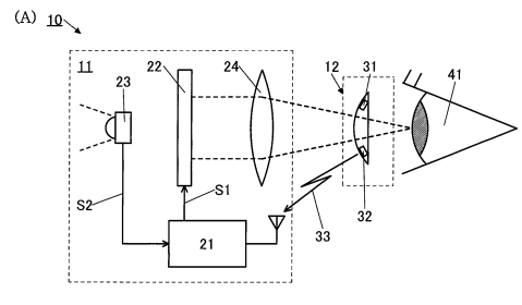
도 1의 (A)에 복합 디바이스(10)의 개략도를 나타내었다. 복합 디바이스(10)는 표시 장치(11)와 센서 장치(12)를 가진다.A schematic diagram of the
표시 장치(11)는 제어부(21), 표시부(22), 촬상부(23), 및 렌즈(24)를 가진다. 센서 장치(12)는 센서부(31)와 통신부(32)를 가진다.The
표시 장치(11)는 인체의 머리에 장착될 수 있도록(장착 가능하게) 구성되어 있는 것이 바람직하다. 예를 들어 안경형 표시 디바이스 또는 고글형 표시 디바이스로서 사용될 수 있다. 또한 한쪽 눈으로 화상을 시인하는 구성이어도 좋다.It is preferable that the
센서 장치(12)는 인체에 장착될 수 있도록(장착 가능하게) 구성되어 있다. 도 1의 (A)에서는 센서 장치(12)가 인체의 안구에 장착될 수 있도록 구성되어 있는 예를 나타내었다. 도 1의 (A)에 나타낸 센서 장치(12)는 콘택트 렌즈로서도 사용될 수 있다. 또한 센서 장치(12)의 구성은 이에 한정되지 않고, 다양한 형태를 취할 수 있다.The
표시 장치(11)가 가지는 표시부(22)는 복수의 화소를 가지고, 화상을 표시하는 기능을 가진다. 화소는 하나 이상의 표시 소자를 가진다. 표시 소자로서는 발광 소자, 액정 소자, 마이크로캡슐, 전기 영동 소자, 일렉트로 웨팅 소자, 전기 유체(electrofluidic) 소자, 일렉트로 크로믹 소자, MEMS 소자 등, 다양한 표시 소자를 사용할 수 있다.The
특히, 표시부(22)가 가지는 표시 소자에 발광 소자를 사용함으로써 높은 콘트라스트를 얻을 수 있기 때문에, 현실감이 더 높은 화상을 표시할 수 있다. 발광 소자로서는 유기 EL 소자, LED 소자, 무기 EL 소자 등을 사용할 수 있다. 특히 유기 EL 소자를 사용하는 것이 바람직하다.In particular, since high contrast can be obtained by using a light emitting element for the display element of the
LED 소자로서는 크기가 큰 것으로부터 매크로 LED(거대 LED라고도 함), 미니 LED, 마이크로 LED 등이 있다. 여기서 LED 칩의 1변의 치수가 1mm를 넘는 것을 매크로 LED라고 부르고, 100μm보다 크고 1mm 이하의 것을 미니 LED라고 부르고, 100μm 이하의 것을 마이크로 LED라고 부른다. 화소에 적용되는 LED 소자로서는 특히 마이크로 LED를 사용하는 것이 바람직하다. 마이크로 LED를 사용함으로써 매우 고정세(高精細)한 표시 장치를 실현할 수 있다.Examples of the LED elements include macro LEDs (also referred to as giant LEDs), mini LEDs, micro LEDs, and the like, from large ones. Here, a LED chip with a side dimension of more than 1 mm is called a macro LED, a thing larger than 100 μm and less than 1 mm is called a mini LED, and a thing smaller than 100 μm is called a micro LED. As the LED element applied to the pixel, it is particularly preferable to use a micro LED. By using the micro LED, a very high-definition display device can be realized.
표시부(22)는 정세도가 높을수록 바람직하다. 표시부(22)의 화소 밀도는 1000ppi 이상 50000ppi 이하, 바람직하게는 2000ppi 이상 20000ppi 이하, 더 바람직하게는 3000ppi 이상 10000ppi 이하, 더욱 바람직하게는 5000ppi 이상 10000ppi 이하로 할 수 있다. 대표적으로는 4500ppi 이상 5500ppi 이하의 화소 밀도, 5500ppi 이상 6500ppi 이하의 화소 밀도, 또는 6500ppi 이상 7500ppi 이하의 화소 밀도로 할 수 있다.As for the
또한 표시부(22)는 해상도가 높을수록 바람직하다. 표시부(22)의 화소수는 주사선 방향 또는 신호선 방향의 화소수가, 예를 들어 1000 이상 20000 이하, 바람직하게는 2000 이상 10000 이하, 더 바람직하게는 3000 이상 10000 이하로 할 수 있다. 표시부(22)를 왼쪽 눈용과 오른쪽 눈용으로 2개 제공하는 경우에는, 표시 영역의 형상을 정방형에 가까운(세로와 가로의 길이의 비율이 0.8 이상 1.2 이하) 형상으로 할 수 있다. 한편으로 하나의 표시 영역을 오른쪽 눈과 왼쪽 눈으로 나누어 사용하는 경우에는 표시 영역의 형상은 가로로 긴 장방형(예를 들어, 세로에 대한 가로의 길이의 비율이 1.5 이상 5.0 이하)으로 하는 것이 바람직하다. 또한 표시부(22)는 종횡비가 16:9인 텔레비전의 규격에 맞추어도 좋고, 이 경우에는 FHD규격, 4K2K규격, 또는 8K4K 규격의 해상도로 할 수 있다.In addition, it is preferable that the
또한 표시부(22)로서 외광을 투과하는, 소위 시스루 패널을 사용하여도 좋다. 이에 의하여 표시 장치(11)를 AR용 기기로서 사용할 수 있다. 이때, 표시 장치(11)에 촬상부(23)를 제공하지 않는 구성으로 하여도 좋다.Moreover, as the
표시 장치(11)가 장착되었을 때, 촬상부(23)는 앞쪽을 촬상할 수 있는 위치에 제공된다. 촬상부(23)로 촬상한 화상은 제어부(21)를 통하여 표시부(22)에 표시할 수 있다.When the
촬상부(23)로서는 카메라를 적합하게 사용할 수 있다. 촬상부(23)가 가지는 촬상 소자는 해상도가 높을수록 바람직하다. 특히, 표시부(22)가 가지는 화소수와 같거나, 또는 그 이상의 화소수를 가지는 것이 바람직하다.As the
제어부(21)는 표시부(22)에 공급하는 화상 신호(S1)를 생성하고 출력하는 기능을 가진다. 제어부(21)는 촬상부(23)의 동작을 제어하는 기능과, 촬상부(23)로부터 입력되는 화상 신호(S2)를 취득하는 기능을 가진다. 제어부(21)는 센서 장치(12)로부터 공급되는 신호(33)를 수신하는 기능과, 상기 신호(33)에 포함되는 정보에 의거하여 표시부(22)에 출력하는 화상 신호(S1)를 생성하는 기능을 가진다.The
예를 들어 제어부(21)는 화상 신호(S2)에 포함되는 촬상부(23)에서 촬상한 화상 데이터에 의거하여, 촬상부(23)에서 촬상된 화상을 거의 지연 없이 표시부(22)에 표시시킬 수 있다. 또한 제어부(21)는 센서 장치(12)에서 취득한 정보에 의거하여, 생성한 화상과 화상 신호(S2)에 포함되는 화상을 합성한 합성 화상을 생성하고 표시부(22)에 상기 합성 화상을 표시시킬 수 있다. 이에 의하여 소위 AR 표시 또는 MR(Mixed Reality, 복합 현실이라고도 함) 표시가 가능해진다.For example, the
센서 장치(12)는 센서부(31)와 통신부(32)를 가진다. 센서 장치(12)는 센서부(31)에서 취득한 정보를, 통신부(32)를 통하여 표시 장치(11)의 제어부(21)에 송신할 수 있다.The
센서부(31)는 다양한 생체 정보를 취득할 수 있는 센서를 가질 수 있다. 예를 들어 센서부는 인체에 닿는 접촉형 센서, 광을 이용한 광학식의 센서, 인체로부터의 전자 신호를 이용한 전기적 센서, 체액(예를 들어 눈물이나 땀 등)의 성분이나 성질을 취득할 수 있는 센서 등을 적용할 수 있다.The
예를 들어 도 1의 (A)에 나타낸 센서 장치(12)에서는 눈물을 바탕으로 센서부(31)에 의하여 염분, 글루코스 등의 농도를 측정할 수 있다. 예를 들어 센서부(31)에 의하여 측정된 글루코스 농도를 바탕으로 사용자의 혈당치를 추정할 수 있다.For example, in the
통신부(32)는 센서부(31)에서 취득한 정보를 포함하는 신호(33)를 표시 장치(11)에 송신하는 기능을 가진다. 통신부(32)는 안테나, 신호 생성 회로, 및 변조 회로 등을 가지는 구성으로 할 수 있다.The
도 1의 (A)에는 사용자의 안구(41)를 명시하였다. 여기서는 이해를 용이하게 하기 위하여, 안구(41)와 센서 장치(12) 사이에 간격을 명시하였지만, 실제로는 센서 장치(12)는 안구(41)에 접촉하도록 장착될 수 있다.In (A) of FIG. 1, the user's
렌즈(24)는 표시부(22)와 센서 장치(12) 사이에 제공되고, 초점을 조정하는 기능을 가진다. 또한 표시부(22)와 안구(41)의 거리가 충분히 떨어져, 초점 조정이 불필요한 경우나, 센서 장치(12)가 초점 조정 기능을 가지는 경우 등에서는 렌즈(24)를 제공하지 않는 구성으로 하여도 좋다.The
사용자는 센서 장치(12) 및 렌즈(24)를 통하여 표시부(22)에 표시되는 화상을 볼 할 수 있다.The user can view the image displayed on the
표시 장치(11)를 머리에 장착하고, 센서 장치(12)를 안구(41)에 장착함으로써, 통신부(25)와 통신부(32)의 통신 거리는 매우 짧은 거리가 된다. 그러므로, 통신에 필요한 전력을 매우 작게 할 수 있기 때문에, 복합 디바이스(10)의 소비 전력을 저감할 수 있다. 또한 통신에 필요한 전력이 작기 때문에, 건강에 대한 통신 전파로 인한 영향을 무시할 수 있을 정도로 작게 할 수 있다.By mounting the
도 1의 (B)에는 복합 디바이스(10)의 블록도를 나타내었다.1B shows a block diagram of the
제어부(21)는 통신부(25)와 화상 생성부(26)를 가진다. 제어부(21)에는 촬상부(23)로부터 화상 신호(S2)가 입력되고, 센서 장치(12)로부터 신호(33)가 입력된다. 또한 외부로부터 화상 신호(S0)가 입력되어도 좋다. 또한 표시부(22)에 제어부(21)로부터 화상 신호(S1)가 출력된다.The
통신부(25)는 센서 장치(12)로부터 송신된 신호(33)를 수신하고, 상기 신호에 포함되는 데이터를 화상 생성부(26)에 출력하는 기능을 가진다. 통신부(25)는 예를 들어 안테나, 복조 회로 등을 가지는 구성으로 할 수 있다.The
또한 통신부(25)와 통신부(32)가 상호 통신이 가능한 구성으로 하는 경우에는 각각이 복조 회로 및 변조 회로를 가지는 구성으로 하면 좋다.In the case where the
통신부(25)는 신호(33)의 입력이 없는 기간에서 동작이 정지한 상태(휴지 상태라고도 함)로 전환되는 기능을 가지는 것이 바람직하다. 이때 제어부(21)는 신호(33)의 입력에 의거하여 통신부(25)를 휴지 상태로부터 복귀시키는 기능을 가진다. 아날로그 회로를 포함하는 통신부(25)를, 동작이 불필요한 기간에 휴지 상태로 함으로써 제어부(21)의 소비 전력을 대폭으로 삭감할 수 있다. 또한 표시 장치(11)의 소형화, 경량화를 실현할 수 있다.It is preferable that the
도 2에는 신호(33)와 통신부(25)의 동작에 따른 타이밍 차트를 모식적으로 나타내었다. 신호(33)의 하나의 신호는 펄스 신호(33a)와 데이터를 포함하는 신호(33b)를 가진다. 도 2에 나타낸 바와 같이 통신부(32)로부터 송신되는 신호(33)는 펄스 신호(33a)와 신호(33b)의 조(set)가 단속적으로 출력되는 신호이다.2 schematically shows a timing chart according to the operation of the
통신부(25)의 동작은 크게 3개로 나누어진 복귀 동작(25a), 처리 동작(25b), 및 휴지 동작(25c)이 한 조를 이룬다. 제어부(21)는 펄스 신호(33a)를 수신하면 통신부(25)에 대하여 복귀 동작(25a)이 실행되도록 제어한다. 통신부(25)는 복귀 동작(25a)에서 휴지 상태로부터 복귀한다. 복귀 동작(25a) 후에 통신부(25)는 처리 동작(25b)에서 수신한 신호(33b)를 복조하고 데이터를 생성하고, 화상 생성부(26)에 출력한다. 출력이 끝나면 통신부(25)는 휴지 동작(25c)을 거쳐 휴지 상태로 이행한다.The operation of the
여기서 도 2에는 동작 기간 Tact와, 휴지 기간 Toff를 나타내었다. 동작 기간 Tact에 대한 휴지 기간 Toff가 길수록 소비 전력을 저감할 수 있다. 예를 들어 사람의 생체 정보의 변화를 감시하는 데 필요한 샘플링 빈도는 10Hz 이하, 5Hz 이하, 1Hz 이하, 또는 0.1Hz 이하로 할 수 있기 때문에 신호(33)의 수신 빈도도 같은 정도로 할 수 있다. 또한 동작 기간 Tact는 매우 짧은 시간(예를 들어 수십μ초 내지 수십m초 정도)으로 할 수 있기 때문에 통신부(25)는 대부분의 기간을 휴지 상태로 할 수 있다.Here, FIG. 2 shows an operation period T act and a rest period T off . Power consumption may be reduced as the idle period T off with respect to the operation period T act is longer. For example, since the sampling frequency required for monitoring the change of human biometric information can be 10 Hz or less, 5 Hz or less, 1 Hz or less, or 0.1 Hz or less, the reception frequency of the
도 1의 (B)에 나타낸 화상 생성부(26)는 통신부(25)로부터 신호(33)에 포함되는 데이터가 입력되면 상기 데이터에 의거하여 화상 데이터를 생성하고, 상기 화상 데이터와 촬상부(23)로부터 입력되는 화상 신호(S2)에 포함되는 화상 데이터를 합성한 합성 화상 데이터를 생성하는 기능을 가진다. 제어부(21)는 상기 합성 화상 데이터를 포함하는 화상 신호(S1)를 생성하고, 표시부(22)에 출력한다.When the data included in the
또한 외부로부터 화상 신호(S0)가 입력되는 구성의 경우, 화상 생성부(26)는 화상 신호(S0)에 포함되는 화상 데이터와, 신호(33)에 포함되는 데이터에 의거하여 생성하는 화상 데이터를 합성한 합성 화상 데이터를 생성하는 기능을 가져도 좋다.In the case of a configuration in which the image signal S0 is inputted from the outside, the
또한 화상 생성부(26)는 화상 신호(S1)에 포함되는 화상 데이터와, 화상 신호(S0)에 포함되는 화상 데이터와, 신호(33)에 포함되는 데이터에 의거하여 생성하는 화상 데이터를 합성한 합성 화상 데이터를 생성하는 기능을 가져도 좋다.In addition, the
[센서 장치에 대하여][About the sensor device]
상기에서는 센서 장치(12)로서 인체의 안구에 장착될 수 있는 구성에 대하여 설명하였지만, 다양한 형태를 취할 수 있다. 이하에서는 센서 장치(12)의 다른 예에 대하여 설명한다.Although the
도 3의 (A)에는 피부에 접착될 수 있도록 구성된 센서 장치(12)를 나타내었다. 도 3의 (A)에서는 센서 장치(12)를 팔(42)에 접착한 상태를 나타내었다. 센서 장치(12)는 각각 칩 형상의 센서부(31)와 통신부(32)를 가진다. 센서 장치(12)의 외장체는 얇은 시트 형상의 부재인 것이 바람직하고, 가요성 또는 신축성을 가지는 것이 바람직하다. 센서 장치(12)는 피부와의 접촉면 측에 점착제를 가지는 구성으로 할 수 있다.3A shows the
도 3의 (B)에는 팔(42)(손목)에 감아 장착될 수 있도록 구성된 센서 장치(12)를 나타내었다. 센서 장치(12)는 적어도 센서부(31)와 통신부(32)를 가진다. 또한 도 3의 (B)에 나타낸 센서 장치(12)는 정보 표시부를 가져도 좋고, 예를 들어 센서 장치(12)가 손목시계형 정보 단말 기기로서 기능하여도 좋다.3B shows a
도 3의 (C)에는 손가락(43)에 장착될 수 있도록 구성된 센서 장치(12)를 나타내었다. 도 3의 (C)에 나타낸 센서 장치(12)는, 적어도 센서부(31)와 통신부(32)를 가진다. 센서 장치(12)는 정보 표시부를 가져도 좋고, 예를 들어 센서 장치(12)가 반지형 정보 단말 기기로서 기능하여도 좋다. 또한 센서 장치(12)가 자이로 센서 등을 가지는 구성으로 함으로써 제스처를 사용한 입력 장치로서 사용하여도 좋다.3C shows the
도 3의 (D)에는 사용자(40)의 상완(44)에 장착될 수 있도록 구성된 센서 장치(12)를 나타내었다. 센서 장치(12)는 적어도 센서부(31)와 통신부(32)를 가진다. 센서 장치(12)는 신축성을 가지는 소재로 구성되는 통 모양, 또는 통의 일부가 빠진 형상(즉, 단면 형상이 대략 C자 형상)의 외장체를 가지는 것이 바람직하다.3D shows the
도 3의 (E)에는 사용자(40)의 옷(45)의 내측에 부착된 센서 장치(12)를 나타내었다. 센서 장치(12)는 적어도 센서부(31)와 통신부(32)를 가진다. 사용자(40)가 옷(45)을 가장 내측에 입었을 때, 센서 장치(12)의 일부가 피부에 접하는 구성인 것이 바람직하다. 또한 센서 장치(12)는 사용자(40)가 옷(45)보다 내측에 다른 옷을 입었을 때도 상기 다른 옷을 통하여 사용자의 생체 정보를 취득할 수 있는 것이 바람직하다. 또한 센서 장치(12)는 옷(45)의 외측에 부착되는 구성, 또는 옷(45)의 내부에 장착되는 구성으로 하여도 좋다.3E shows the
여기서 센서 장치(12)는 혈당치, 심박, 맥박, 혈압, 체온, 산소 포화도, 및 중성 지방 농도 중 하나 이상을 검출하는 기능을 가지는 것이 바람직하다. 혈당치는 상술한 바와 같이 체액 중의 글루코스 농도를 측정함으로써 추정될 수 있다.Here, the
또한 동맥(세동맥)은 혈중 산소 포화도의 변동에 따라 적외광 또는 가시광에 대한 반사율이 변화되기 때문에 광학적으로 측정할 수 있다. 이 변화를 시간의 경과에 따라 취득, 즉, 혈중 산소 포화도의 시간 변조를 취득함으로써, 맥파의 정보를 취득할 수 있다. 이에 의하여 사용자의 심박수를 측정할 수 있다. 또한 적외광 또는 가시광에 의하여 혈중의 중성 지방 농도나, 혈중 또는 진피 중의 글루코스 농도 등을 검출할 수 있다.In addition, the arterioles (arterioles) can be measured optically because the reflectance for infrared or visible light changes according to fluctuations in blood oxygen saturation. Pulse wave information can be acquired by acquiring this change over time, that is, acquiring temporal modulation of blood oxygen saturation. Accordingly, the heart rate of the user may be measured. In addition, the concentration of triglycerides in the blood, the concentration of glucose in the blood or the dermis, etc. can be detected by infrared or visible light.
또한 센서부(31)로서 피부에 접촉하는 전극을 가지는 구성으로 함으로써 심전도를 측정할 수 있다.In addition, the electrocardiogram can be measured by setting it as the structure which has an electrode contacting skin as the
또한 혈압은 심전도와 맥파의 두 박동 타이밍의 어긋남(맥파 전반 시간의 길이)으로 산출할 수 있다. 혈압이 높으면 맥파 전반 시간이 짧고, 반대로 혈압이 낮으면 맥파 전반 시간이 길다. 또한 심전도 및 맥파으로 산출되는 심박수와 혈압의 관계로부터, 사용자의 신체 상태를 추정할 수도 있다. 예를 들어 심박수와 혈압이 둘 다 높으면, 긴장이나 흥분 상태인 것으로 추정할 수 있고, 반대로 심박수와 혈압이 둘 다 낮으면, 긴장이 풀리고 편안한 상태인 것으로 추정할 수 있다. 또한 혈압이 낮으며 심박수가 높은 상태가 계속되는 경우에는 심장 질환 등의 가능성이 있다.In addition, the blood pressure may be calculated as a deviation between the timing of two beats of the electrocardiogram and the pulse wave (the length of the first half of the pulse wave). When blood pressure is high, the first half time of the pulse wave is short, and conversely, when the blood pressure is low, the first half time of the pulse wave is long. In addition, the user's physical state may be estimated from the relationship between the heart rate and blood pressure calculated from the electrocardiogram and pulse wave. For example, when both heart rate and blood pressure are high, it can be estimated that the person is in a tense or excited state, and conversely, when both heart rate and blood pressure are low, it can be estimated that the state is relaxed and relaxed. Also, if blood pressure is low and heart rate is high, there is a possibility of heart disease.
또한 센서 장치(12) 또는 표시 장치(11)에 다른 생체 정보를 취득하는 방법을 제공하는 것이 바람직하다. 예를 들어 심전도, 혈압, 체온 등의 체내의 생체 정보 외, 표정, 얼굴색, 동공 등의 표면적인 생체 정보 등이 있다. 또한 보수나 운동 강도, 이동의 고저차, 식사(섭취한 칼로리나 영양소 등)의 정보도 건강 관리에는 중요한 정보이다. 복수의 생체 정보 등을 사용함으로써 복합적인 몸 관리가 가능해지고, 일상적인 건강 관리뿐만 아니라 부상과 질병의 조기 발견으로도 이어진다.It is also desirable to provide a method for acquiring other biometric information to the
또한 센서 장치(12)가 GPS(Global Positioning System, 위성 위치 확인 시스템이라고도 함)를 가지고, 위치 정보를 취득 가능한 구성으로 하여도 좋다. 또한 센서 장치(12)가 전자 결제를 가지는 기능을 가져도 좋다.In addition, the
[화상의 예][Example of image]
이하에서는 복합 디바이스(10)에 의하여 사용자에게 제시할 수 있는 화상의 일례에 대하여 설명한다.Hereinafter, an example of an image that can be presented to a user by the
도 4의 (A)에는 식사 중의 사용자의 시계에 비치는 화상(50a)의 예를 나타내었다. 화상(50a) 중에는 촬상부(23)에서 촬상되는 현실의 화상과 중첩되어 화상 정보(51a)가 나타내어졌다. 도 4의 (A)에 나타낸 화상 정보(51a)에는 혈당치를 의도한 아이콘 화상(각사탕을 모방한 화상)과, 혈당치가 높은 것을 사용자에게 경고하기 위한 코멘트와, 추정된 혈당치가 제시되었다(CAUTION!! 140mg/dL). 사용자는 화상 정보(51a)에 의하여 자신의 혈당치가 높은 것을 인식하고, 식사의 양을 억제하거나, 후식의 주문을 취소하거나, 혈당치의 상승을 억제하는 음료를 주문하는 등의 행동을 취할 수 있다.4A shows an example of the
도 4의 (B)에는 하이킹 중의 사용자의 시계에 비치는 화상(50b)의 예를 나타내었다. 화상(50b) 중에는 화상 정보(51b)가 나타내어졌다. 화상 정보(51b)에는 심박수를 의도한 아이콘 화상(하트를 모방한 화상)과, 심박수가 높은 것을 사용자에게 경고하기 위한 코멘트와, 측정된 심박수의 값이 제시되었다(CAUTION!! 130bpm). 사용자는 화상 정보(51b)에 의하여 자신의 심박수를 확인할 수 있고, 휴식을 취하거나, 보행 속도를 늦추는 등의 행동을 취할 수 있다.Fig. 4B shows an example of an
도 4의 (C)에는 부하 직원을 불러내 질책하는 사용자의 시계에 비치는 화상(50c)의 예를 나타내었다. 화상(50c) 중에는 화상 정보(51c)가 나타내어졌다. 화상 정보(51c)에는 혈압을 의도한 아이콘 화상(하트와 심전도를 모방한 화상)과, 혈압이 높은 것을 사용자에게 경고하기 위한 코멘트와, 추정된 혈압값이 제시되었다(CAUTION!! 160mmHg). 사용자는 화상 정보(51c)에 의하여 자신이 현저한 흥분 상태에 있는 것을 자각할 수 있고, 분노를 참을 수 있게 심호흡을 하거나, 부하 직원을 대하는 방법을 재검토하는 등의 행동을 취할 수 있다.Fig. 4C shows an example of an
또한 상기에서는 사용자에게 경고하기 위한 코멘트를 명시하는 예를 나타내었지만, 구체적인 행동을 재촉하는 표시를 수행하여도 좋다. 예를 들어 도 4의 (C)에 나타낸 상황에서는 심호흡을 하도록 재촉하는 코멘트나, 애니메이션 화상 등을 제시하여도 좋다.In addition, although an example of specifying a comment to warn the user has been shown above, a display to prompt a specific action may be performed. For example, in the situation shown in FIG.4(C), you may present a comment, an animation image, etc. which urge to take a deep breath.
[변형예][Variation]
이하에서는 상기 구성예의 변형예에 대하여 설명한다.Hereinafter, a modified example of the structural example will be described.
도 5의 (A)에 복합 디바이스(10a)의 개략도를 나타내고, 도 5의 (B)에 복합 디바이스(10a)의 블록도를 나타내었다.A schematic diagram of the
복합 디바이스(10a)는 화상 표시 기능을 가지는 센서 장치(12a)와 정보 처리 장치(13)를 가진다.The
센서 장치(12a)는 센서부(31) 및 통신부(32)에 더하여 표시부(34)를 가진다. 표시부(34)는 화상을 표시하는 기능을 가진다. 표시부(34)로서는 시스루 디스플레이를 적합하게 사용할 수 있다.The
통신부(32)는 센서부(31)에서 취득한 정보를 포함하는 신호(33)를 정보 처리 장치(13)에 송신하는 기능을 가진다. 또한 정보 처리 장치(13)로부터 수신한 신호(27)를 복조하고, 신호(27)에 포함되는 화상 신호를 표시부(34)에 출력하는 기능을 가진다.The
표시부(34)는 통신부(32)로부터 입력된 화상 신호에 의거하여 화상을 표시할 수 있다.The
정보 처리 장치(13)는 제어부(21)를 가진다. 제어부(21)는 통신부(25)와 화상 생성부(26)를 가진다.The
통신부(25)는 센서 장치(12a)로부터 송신된 신호(33)를 수신하고, 상기 신호에 포함되는 데이터를 화상 생성부(26)에 출력하는 기능을 가진다. 또한 통신부(25)는 화상 생성부(26)로부터 입력된 화상 신호(S1)를 포함하는 신호(27)를 센서 장치(12a)에 송신하는 기능을 가진다.The
화상 생성부(26)는 통신부(25)로부터 신호(33)에 포함되는 데이터가 입력되면 상기 데이터에 의거하여 화상 신호(S1)를 생성하고 통신부(25)에 출력하는 기능을 가진다.When data included in the
사용자는 센서 장치(12a)를 투과한 투과상과 중첩하여 표시부(34)에 표시되는 화상을 볼 수 있다. 복합 디바이스(10a)는 사용자에게 AR 표시를 제시할 수 있다. 또한 표시부(34)가 광을 투과하지 않는 구성으로 하고 사용자에게 VR 표시를 제시하여도 좋다.The user can view the image displayed on the
이와 같은 구성으로 함으로써 복합 디바이스(10a)의 구성을 극히 간략화할 수 있다. 또한 정보 처리 장치(13)는 소형화, 경량화가 용이하므로 주머니나 가방에 넣을 수도 있다. 이때, 머리에 장착하는 장치는 불필요하므로 사용자가 번거롭게 느끼지 않는 디바이스로 할 수 있다.By setting it as such a structure, the structure of the
본 실시형태는 적어도 그 일부를 본 명세서에 기재된 다른 실시형태와 적절히 조합하여 실시할 수 있다.This embodiment can be implemented by suitably combining at least a part of it with other embodiment described in this specification.
(실시형태 2)(Embodiment 2)
본 실시형태에서는 본 발명의 일 형태의 복합 디바이스에 사용할 수 있는 표시 장치를 가지는 전자 기기의 구성예에 대하여 설명한다.In this embodiment, the structural example of the electronic device which has a display apparatus which can be used for the composite device of one embodiment of this invention is demonstrated.
도 6의 (A)에는 안경형 전자 기기(900)의 사시도를 나타내었다. 전자 기기(900)는 한 쌍의 표시 패널(901), 한 쌍의 하우징(하우징(902a), 하우징(902b)), 한 쌍의 광학 부재(903), 한 쌍의 장착부(904) 등을 가진다.6A is a perspective view of the spectacle-type
전자 기기(900)는 광학 부재(903)의 표시 영역(906)에, 표시 패널(901)에 표시한 화상을 투영할 수 있다. 또한 광학 부재(903)는 투광성을 가지기 때문에 사용자는 광학 부재(903)를 통하여 시인되는 투과 이미지에 겹쳐 표시 영역(906)에 표시된 화상을 볼 수 있다. 따라서 전자 기기(900)는 AR 표시가 가능한 전자 기기이다.The
또한 하나의 하우징(902a)에는 앞쪽을 촬상할 수 있는 카메라(905)가 제공된다. 또한 하우징(902a)에는 무선 통신기(907)를 가지고 하우징(902a) 및 하우징(902b)에 영상 신호 등을 공급할 수 있다. 또한 무선 통신기(907) 대신에 또는 무선 통신기(907)에 더하여 영상 신호나 전원 전위가 공급되는 케이블을 접속 가능한 커넥터를 가져도 좋다. 또한 하우징(902a) 또는 하우징(902b)에 자이로 센서 등의 가속도 센서를 가짐으로써 사용자의 머리의 방향을 검지하고, 그 방향에 따른 화상을 표시 영역(906)에 표시할 수도 있다. 또한 하우징(902a) 또는 하우징(902b)에는 배터리가 제공되는 것이 바람직하고, 무선 또는 유선으로 충전할 수 있다.Also, one
또한 하우징(902b)에는 프로세서(908)가 제공된다. 프로세서(908)는 카메라(905), 무선 통신기(907), 한 쌍의 표시 패널(901) 등, 전자 기기(900)가 가지는 각종 컴포넌트를 제어하는 기능이나, 화상을 생성하는 기능 등을 가진다. 프로세서(908)는 AR 표시를 위한 합성 화상을 생성하는 기능을 가져도 좋다.A
무선 통신기(907)에 의하여 외부의 기기와 데이터의 통신을 수행할 수 있다. 예를 들어 외부로부터 송신되는 데이터를 프로세서(908)에 출력하고, 프로세서(908)는 상기 데이터에 의거하여 AR 표시를 위한 화상 데이터를 생성할 수도 있다. 외부로부터 송신되는 데이터의 예로서는 화상 데이터 외, 생체 센서 장치 등으로부터 송신되는 생체 정보를 포함하는 데이터 등을 들 수 있다.The
이어서 도 6의 (B)를 사용하여, 전자 기기(900)의 표시 영역(906)으로의 화상의 투영 방법에 대하여 설명한다. 하우징(902)(하우징(902a) 및 하우징(902b))의 내부에는 표시 패널(901), 렌즈(911), 반사판(912)이 제공된다. 또한 광학 부재(903)의 표시 영역(906)에 상당하는 부분에는 하프 미러로서 기능하는 반사면(913)을 가진다.Next, a method of projecting an image onto the
표시 패널(901)로부터 방출된 광(915)은 렌즈(911)를 통과하여 반사판(912)에 의하여 광학 부재(903) 측으로 반사된다. 광학 부재(903)의 내부에 있어서, 광(915)은 광학 부재(903)의 단부면에서 전반사를 반복하여 반사면(913)에 도달함으로써 반사면(913)에 화상이 투영된다. 이에 의하여, 사용자는 반사면(913)에 반사된 광(915)과 광학 부재(903)(반사면(913)을 포함함)를 투과한 투과광(916)의 양쪽을 시인할 수 있다.The light 915 emitted from the
도 6의 (B)에는 반사판(912)의 표면 및 반사면(913)이 각각 곡면을 가지는 예를 나타내었다. 이로써, 이들이 평면인 경우에 비하여 광학 설계의 자유도를 높일 수 있고, 광학 부재(903)의 두께를 얇게 할 수 있다. 또한 반사판(912)의 표면 및 반사면(913)을 평면으로 하여도 좋다.6B shows an example in which the surface of the
반사판(912)으로서는 경면을 가지는 부재를 사용할 수 있고, 반사율이 높은 것이 바람직하다. 또한 반사면(913)으로서는 금속막의 반사를 이용한 하프 미러를 사용하여도 좋지만, 전반사를 이용한 프리즘 등을 사용하면 투과광(916)의 투과율을 높일 수 있다.As the reflecting
여기서 하우징(902)은 렌즈(911)와 표시 패널(901) 사이의 거리나 이들의 각도를 조정하는 기구를 가지는 것이 바람직하다. 이로써, 초점의 조정이나 화상의 확대, 축소 등의 조작을 수행할 수 있게 된다. 예를 들어, 렌즈(911) 및 표시 패널(901) 중 한쪽 또는 양쪽이 광축 방향으로 이동할 수 있는 구성으로 하면 좋다.Here, the
또한 하우징(902)은 반사판(912)의 각도를 조정할 수 있는 기구를 가지는 것이 바람직하다. 반사판(912)의 각도를 바꿈으로써, 화상이 표시되는 표시 영역(906)의 위치를 바꿀 수 있게 된다. 이로써, 사용자의 눈의 위치에 따라 최적의 위치에 표시 영역(906)을 배치할 수 있게 된다.In addition, it is preferable that the
표시 패널(901)에는 본 발명의 일 형태의 표시 장치 또는 표시 모듈을 적용할 수 있다. 따라서 정세도가 매우 높은 표시가 가능한 전자 기기(900)로 할 수 있다.The display device or display module of one embodiment of the present invention can be applied to the
도 7의 (A), (B)에는 고글형 전자 기기(950)의 사시도를 나타내었다. 도 7의 (A)는 전자 기기(950)의 정면, 평면 및 왼쪽 면을 나타낸 사시도이고, 도 7의 (B)는 전자 기기(950)의 배면, 저면, 및 오른쪽 면을 나타낸 사시도이다.7A and 7B are perspective views of the goggle-type
전자 기기(950)는 한 쌍의 표시 패널(951), 하우징(952), 한 쌍의 장착부(954), 완충 부재(955), 한 쌍의 렌즈(956) 등을 가진다. 한 쌍의 표시 패널(951)은 하우징(952)의 내부의 렌즈(956)를 통하여 시인할 수 있는 위치에 각각 제공된다.The
전자 기기(950)는 VR용 전자 기기이다. 전자 기기(950)를 장착한 사용자는 렌즈(956)를 통하여 표시 패널(951)에 표시되는 화상을 시인할 수 있다. 또한 한 쌍의 표시 패널(951)에 상이한 화상을 표시시킴으로써, 시차를 사용한 3차원 표시를 수행할 수도 있다. 또한 전자 기기(950)가 가지는 하우징(952)에 방수 기능을 적용하고, 전자 기기(950)를 수중에서도 사용할 수 있는 구성으로 하여도 좋다. 이때, 하우징(952)의 형상을 유선형으로 하면 물의 저항을 저감할 수 있어, 더 빠르게 헤엄칠 수 있기 때문에 바람직하다.The
또한 하우징(952)의 배면 측에는 입력 단자(957)와 출력 단자(958)가 제공된다. 입력 단자(957)에는 영상 출력 기기 등으로부터의 영상 신호나 하우징(952) 내에 제공되는 배터리를 충전하기 위한 전력 등을 공급하는 케이블을 접속할 수 있다. 출력 단자(958)로서는 예를 들어 음성 출력 단자로서 기능하고, 이어폰이나 헤드폰 등을 접속할 수 있다. 또한 무선 통신에 의하여 음성 데이터를 출력할 수 있는 구성으로 하는 경우나, 외부의 영상 출력 기기로부터 음성을 출력하는 경우에는, 상기 음성 출력 단자를 제공하지 않아도 된다.In addition, an
하우징(952)에는 앞쪽을 촬상할 수 있는 카메라(959)가 제공된다. 전자 기기(950)는 카메라(959)로 촬상한 화상, 또는 상기 화상을 사용한 합성 화상을 표시할 수 있다. 전자 기기(950)는 VR 표시뿐만 아니라 AR 표시, MR 표시도 수행할 수 있다.The
또한 하우징(952)에는 프로세서(961)와 무선 통신기(962)가 제공된다. 프로세서(961)에 의하여 한 쌍의 표시 패널(951), 카메라(959), 무선 통신기(962) 등, 전자 기기(950)가 가지는 각종 컴포넌트를 제어할 수 있다. 또한 프로세서(961)에 의하여 표시 패널(951)에 표시하기 위한 화상을 생성할 수 있다.A
또한 무선 통신기(962)에 의하여 외부의 기기와 데이터의 통신을 수행할 수 있다. 예를 들어 외부로부터 송신되는 데이터를 프로세서(961)에 출력하고, 프로세서(961)는 상기 데이터에 의거하여 VR 표시, AR 표시, 또는 MR 표시를 위한 화상 데이터를 생성할 수도 있다. 외부로부터 송신되는 데이터의 예로서는, 화상 데이터 외, 생체 센서 장치 등으로부터 송신되는 생체 정보를 포함하는 데이터 등을 들 수 있다.In addition, data communication with an external device may be performed by the
또한 하우징(952)은 렌즈(956) 및 표시 패널(951)이 사용자의 눈의 위치에 따라 최적의 위치가 되도록 이들의 좌우의 위치를 조정할 수 있는 기구를 가지는 것이 바람직하다. 또한 렌즈(956)와 표시 패널(951) 사이의 거리를 바꿈으로써 초점을 조정하는 기구를 가지는 것이 바람직하다.In addition, it is preferable that the
표시 패널(951)에는 본 발명의 일 형태의 표시 장치 또는 표시 모듈을 적용할 수 있다. 따라서 정세도가 매우 높은 표시가 가능한 전자 기기(950)로 할 수 있다. 이로써, 사용자가 높은 몰입감을 느낄 수 있다.The display device or display module of one embodiment of the present invention can be applied to the
완충 부재(955)는 사용자 얼굴(이마나 볼 등)에 접촉하는 부분이다. 완충 부재(955)가 사용자 얼굴과 밀착함으로써 광누설을 방지할 수 있어, 몰입감을 더 높일 수 있다. 완충 부재(955)는 사용자가 전자 기기(950)를 장착할 때 사용자의 얼굴에 밀착하도록, 부드러운 소재를 사용하는 것이 바람직하다. 예를 들어 고무, 실리콘(silicone) 고무, 우레탄, 스펀지 등의 소재를 사용할 수 있다. 또한 스펀지 등의 표면을 천이나 가죽(천연 피혁 또는 합성 피혁) 등으로 덮은 것을 사용하면, 사용자 얼굴과 완충 부재(955) 사이에 틈이 생기기 어려워 광누설을 적합하게 방지할 수 있다. 또한 이와 같은 소재를 사용하면, 촉감이 좋으면서, 추운 계절 등에 장착할 때에 사용자가 차가움을 느끼지 않기 때문에 바람직하다. 완충 부재(955)나 장착부(954) 등의, 사용자 피부에 접촉되는 부재는 탈착 가능한 구성으로 하면 클리닝이나 교환이 용이하기 때문에 바람직하다.The
본 실시형태는 적어도 그 일부를 본 명세서에 기재된 다른 실시형태와 적절히 조합하여 실시할 수 있다.This embodiment can be implemented by suitably combining at least a part of it with other embodiment described in this specification.
(실시형태 3)(Embodiment 3)
본 실시형태에서는 본 발명의 일 형태의 복합 디바이스에 적용할 수 있는 표시 패널의 구성예에 대하여 설명한다. 이하에서 예시하는 표시 패널은 매우 높은 정세도를 실현할 수 있기 때문에, 표시 장치 또는 센서 장치가 가지는 표시부에 적합하게 사용할 수 있다.In the present embodiment, a configuration example of a display panel applicable to the composite device of one embodiment of the present invention will be described. Since the display panel illustrated below can realize a very high definition, it can be suitably used for a display part of a display device or a sensor device.
[화소의 구성예][Example of configuration of pixels]
이하에서는 고정세한 표시 패널에 적절한 화소의 배열 방법의 예에 대하여 설명한다.Hereinafter, an example of a method for arranging pixels suitable for a high-definition display panel will be described.
예를 들어 이하에 나타내는 구성에서는, 발광 소자를 포함하는 화소가 1000ppi 이상 50000ppi 이하, 바람직하게는 2000ppi 이상 20000ppi 이하, 더 바람직하게는 3000ppi 이상 10000ppi 이하, 더욱 바람직하게는 5000ppi 이상 10000ppi 이하의 정세도(화소 밀도)로 표시 영역에 배치된 표시 장치를 실현할 수 있다. 대표적으로는 4500ppi 이상 5500ppi 이하의 화소 밀도, 5500ppi 이상 6500ppi 이하의 화소 밀도, 또는 6500ppi 이상 7500ppi 이하의 화소 밀도로 할 수 있다.For example, in the configuration shown below, a pixel including a light emitting element has a fineness of 1000 ppi or more and 50000 ppi or less, preferably 2000 ppi or more and 20000 ppi or less, more preferably 3000 ppi or more and 10000 ppi or less, still more preferably 5000 ppi or more and 10000 ppi or less ( A display device arranged in a display area with a pixel density) can be realized. Typically, a pixel density of 4500 ppi or more and 5500 ppi or less, a pixel density of 5500 ppi or more and 6500 ppi or less, or a pixel density of 6500 ppi or more and 7500 ppi or less.
[화소 회로의 구성예][Configuration example of pixel circuit]
도 8의 (A)에는 화소 유닛(70)의 회로도의 예를 나타내었다. 화소 유닛(70)은 2개의 화소(화소(70a) 및 화소(70b))로 구성된다. 또한 화소 유닛(70)에는 배선(91a), 배선(91b), 배선(92a), 배선(92b), 배선(92c), 배선(92d), 배선(93a), 배선(93b), 배선(93c) 등이 접속되어 있다.8A shows an example of a circuit diagram of the
화소(70a)는 부화소(71a), 부화소(72a), 및 부화소(73a)를 가진다. 화소(70b)는 부화소(71b), 부화소(72b), 및 부화소(73b)를 가진다. 부화소(71a), 부화소(72a), 및 부화소(73a)는 각각 화소 회로(81a), 화소 회로(82a), 및 화소 회로(83a)를 가진다. 또한 부화소(71b), 부화소(72b), 및 부화소(73b)는 각각 화소 회로(81b), 화소 회로(82b), 및 화소 회로(83b)를 가진다.The
각 부화소는 화소 회로와 표시 소자(60)를 가진다. 예를 들어 부화소(71a)는 화소 회로(81a)와 표시 소자(60)를 가진다. 여기서는 표시 소자(60)로서 유기 EL 소자 등의 발광 소자를 사용한 경우를 나타낸다.Each sub-pixel has a pixel circuit and a
배선(91a) 및 배선(91b)은 각각 주사선(게이트선이라고도 함)으로서의 기능을 가진다. 배선(92a), 배선(92b), 배선(92c), 및 배선(92d)은 각각 신호선(소스선 또는 데이터선이라고도 함)으로서의 기능을 가진다. 또한 배선(93a), 배선(93b), 및 배선(93c)은 표시 소자(60)에 전위를 공급하는 기능을 가진다.The
화소 회로(81a)는 배선(91a), 배선(92a), 및 배선(93a)과 전기적으로 접속되어 있다. 화소 회로(82a)는 배선(91b), 배선(92d), 및 배선(93a)과 전기적으로 접속되어 있다. 화소 회로(83a)는 배선(91a), 배선(92b), 및 배선(93b)과 전기적으로 접속되어 있다. 화소 회로(81b)는 배선(91b), 배선(92a), 및 배선(93b)과 전기적으로 접속되어 있다. 화소 회로(82b)는 배선(91a), 배선(92c), 및 배선(93c)과 전기적으로 접속되어 있다. 화소 회로(83b)는 배선(91b), 배선(92b), 및 배선(93c)과 전기적으로 접속되어 있다.The
도 8의 (A)에 나타낸 바와 같이, 하나의 화소에 2개의 게이트선이 접속되는 구성으로 함으로써, 반대로 소스선의 개수를 스트라이프 배치와 비교하여 반으로 할 수 있다. 이에 의하여, 소스 구동 회로로서 사용하는 IC의 개수를 반으로 줄일 수 있어, 부품 점수를 삭감할 수 있다.As shown in Fig. 8A, by configuring two gate lines to be connected to one pixel, on the contrary, the number of source lines can be halved compared with the stripe arrangement. Thereby, the number of ICs used as the source driving circuit can be cut in half, and the number of parts can be reduced.
또한 신호선으로서 기능하는 하나의 배선에는 같은 색에 대응한 화소 회로를 접속하는 구성으로 하는 것이 바람직하다. 예를 들어, 화소 간의 휘도의 편차를 보정하기 위하여 전위가 조정된 신호를 상기 배선에 공급하는 경우, 보정값은 색마다 크게 달라지는 경우가 있다. 그러므로 하나의 신호선에 접속되는 화소 회로를, 모두 같은 색에 대응한 화소 회로로 함으로써, 용이하게 보정할 수 있다.Furthermore, it is preferable to configure one wiring serving as a signal line to connect pixel circuits corresponding to the same color. For example, when a signal whose potential is adjusted is supplied to the wiring in order to correct a luminance deviation between pixels, the correction value may vary greatly for each color. Therefore, by making the pixel circuits connected to one signal line all pixel circuits corresponding to the same color, correction can be made easily.
또한 각 화소 회로는 트랜지스터(61)와, 트랜지스터(62)와, 용량 소자(63)를 가진다. 예를 들어 화소 회로(81a)에서 트랜지스터(61)는 게이트가 배선(91a)과 전기적으로 접속되고, 소스 및 드레인 중 한쪽이 배선(92a)과 전기적으로 접속되고, 소스 및 드레인 중 다른 쪽이 트랜지스터(62)의 게이트 및 용량 소자(63)의 한쪽 전극과 전기적으로 접속되어 있다. 트랜지스터(62)는 소스 및 드레인 중 한쪽이 표시 소자(60)의 한쪽 전극과 전기적으로 접속되고, 소스 및 드레인 중 다른 쪽이 용량 소자(63)의 다른 쪽 전극 및 배선(93a)과 전기적으로 접속되어 있다. 표시 소자(60)의 다른 쪽 전극은 전위(V1)가 공급되는 배선과 전기적으로 접속되어 있다.In addition, each pixel circuit includes a
또한 다른 화소 회로에 대해서는 도 8의 (A)에 나타낸 바와 같이 트랜지스터(61)의 게이트가 접속되는 배선, 트랜지스터(61)의 소스 및 드레인 중 한쪽이 접속되는 배선, 및 용량 소자(63)의 다른 쪽 전극이 접속되는 배선이 다르다는 점 이외에는 화소 회로(81a)와 마찬가지의 구성을 가진다.As for the other pixel circuits, as shown in FIG. 8A , the wiring to which the gate of the
도 8의 (A)에서 트랜지스터(61)는 선택 트랜지스터로서의 기능을 가진다. 또한 트랜지스터(62)는 표시 소자(60)와 직렬 접속되고, 표시 소자(60)에 흐르는 전류를 제어하는 기능을 가진다. 용량 소자(63)는 트랜지스터(62)의 게이트가 접속되는 노드의 전위를 유지하는 기능을 가진다. 또한 트랜지스터(61)의 오프 상태에서의 누설 전류나, 트랜지스터(62)의 게이트를 통한 누설 전류 등이 매우 작은 경우에는 용량 소자(63)를 의도적으로 제공하지 않아도 된다.In FIG. 8A , the
여기서 도 8의 (A)에 나타낸 바와 같이, 트랜지스터(62)는 각각 전기적으로 접속된 제 1 게이트와 제 2 게이트를 가지는 구성으로 하는 것이 바람직하다. 이와 같이 2개의 게이트를 가지는 구성으로 함으로써, 트랜지스터(62)가 흐르게 할 수 있는 전류를 증대시킬 수 있다. 특히 고정세한 표시 장치에서는 트랜지스터(62)의 크기, 특히 채널 폭을 크게 하지 않아도 상기 전류를 증대시킬 수 있어 바람직하다.Here, as shown in Fig. 8A, the
또한 트랜지스터(62)가 하나의 게이트를 가지는 구성으로 하여도 좋다. 이와 같은 구성으로 함으로써 제 2 게이트를 형성하는 공정이 불필요하게 되므로 상기와 비교하여 공정을 간략화할 수 있다. 또한 트랜지스터(61)가 2개의 게이트를 가지는 구성으로 하여도 좋다. 이와 같은 구성으로 함으로써, 어느 트랜지스터도 크기를 작게 할 수 있다. 또한 각 트랜지스터의 제 1 게이트와 제 2 게이트가 각각 전기적으로 접속되는 구성으로 할 수 있다. 또는 한쪽의 게이트가 다른 배선과 전기적으로 접속되는 구성으로 하여도 좋다. 그 경우, 상기 배선에 공급하는 전위를 다르게 함으로써 트랜지스터의 문턱 전압을 제어할 수 있다.Further, the
또한 표시 소자(60)의 한 쌍의 전극 중 트랜지스터(62)와 전기적으로 접속되는 전극이 화소 전극에 상당한다. 여기서 도 8의 (A)에서는 표시 소자(60)의 트랜지스터(62)와 전기적으로 접속되는 전극을 음극, 반대 측의 전극을 양극으로 한 구성을 나타내었다. 이와 같은 구성은 트랜지스터(62)가 n채널형 트랜지스터인 경우에 특히 효과적이다. 즉, 트랜지스터(62)가 온 상태일 때, 배선(93a)에 의하여 공급되는 전위가 소스 전위가 되기 때문에 표시 소자(60)의 저항의 편차나 변동에 상관없이 트랜지스터(62)에 흐르는 전류를 일정하게 할 수 있다. 또한 화소 회로가 가지는 트랜지스터로서 p채널형 트랜지스터를 사용하여도 좋다.Also, among the pair of electrodes of the
[표시 소자의 구성예][Configuration example of display element]
도 8의 (B)는 표시 소자의 배치 방법의 예를 나타낸 상면 개략도이다. 도 8의 (B)에는 2 화소 유닛 분의 상면 개략도를 나타내었다.Fig. 8B is a schematic top view showing an example of a method of arranging a display element. 8B is a schematic top view of 2 pixel units.
화소(70a)는 표시 소자(R1), 표시 소자(G1), 및 표시 소자(B1)를 가진다. 화소(70b)는 표시 소자(R2), 표시 소자(G2), 및 표시 소자(B2)를 가진다. 표시 소자(R1) 및 표시 소자(R2)는 적색을 나타내는 표시 소자이고, 표시 소자(G1) 및 표시 소자(G2)는 녹색을 나타내는 표시 소자이고, 표시 소자(B1) 및 표시 소자(B2)는 청색을 나타내는 표시 소자이다.The
표시 소자(R1) 및 표시 소자(R2)에 척안하면 세로 방향으로 지그재그로 배치되어 있다. 마찬가지로 표시 소자(G1)와 표시 소자(G2), 표시 소자(B1)와 표시 소자(B2)도 각각 지그재그로 배치되어 있다. 이와 같은 구성으로 함으로써 시야각 의존성이 개선되고, 표시면에 대하여 비스듬한 방향으로부터 보았을 때, 색도나 휘도의 어긋남이 생기기 어렵다는 효과가 나타난다.The display elements R1 and R2 are arranged in a zigzag manner in the vertical direction when the display elements R1 and R2 are counted. Similarly, the display element G1 and the display element G2, and the display element B1 and the display element B2 are respectively arranged in a zigzag manner. By setting it as such a structure, the viewing angle dependence is improved, and when it sees from the direction oblique with respect to a display surface, the effect that chromaticity or a luminance shift is hard to produce appears.
여기까지가 화소의 구성예에 대한 설명이다.This is the description of the configuration example of the pixel.
[표시 모듈의 구성예][Example of configuration of display module]
이하에서는 본 발명의 일 형태의 표시 모듈의 구성예에 대하여 설명한다.Hereinafter, a configuration example of a display module of one embodiment of the present invention will be described.
도 9의 (A)는 표시 모듈(280)의 사시 개략도이다. 표시 모듈(280)은 표시 장치(200)와 FPC(290)를 가진다.9A is a perspective schematic view of the
표시 모듈(280)은 기판(201), 기판(202)을 가진다. 또한 기판(202) 측에 표시부(281)를 가진다. 표시부(281)는 표시 모듈(280)에서의 화상을 표시하는 영역이고, 후술하는 화소부(284)에 제공되는 각 화소로부터의 광을 시인할 수 있는 영역이다.The
도 9의 (B)에 기판(201) 측의 구성을 모식적으로 나타낸 사시도를 나타내었다. 기판(201)은 회로부(282)와, 회로부(282) 위에 화소 회로부(283)와, 화소 회로부(283) 위에 화소부(284)가 적층된 구성을 가진다. 또한 기판(201) 위에서 화소부(284)와 중첩되지 않는 부분에 FPC(290)와 접속하기 위한 단자부(285)를 가진다. 또한 단자부(285)와 회로부(282)는 복수의 배선으로 구성되는 배선부(286)에 의하여 전기적으로 접속된다.Fig. 9B is a perspective view schematically showing the configuration of the
화소부(284)는 매트릭스로 배열된 복수의 화소(284a)를 가진다. 도 9의 (B)의 오른쪽에, 하나의 화소(284a)의 확대도를 나타내었다. 화소(284a)는 표시 소자(R1), 표시 소자(G1), 표시 소자(B1), 표시 소자(R2), 표시 소자(G2), 및 표시 소자(B2)를 가진다. 화소(284a)는 상기 도 8의 (A), (B)에서 예시한 화소 유닛(70)에 상당한다.The
화소 회로부(283)는 매트릭스로 배열된 복수의 화소 회로(283a)를 가진다. 하나의 화소 회로(283a)는 하나의 화소(284a)가 가지는 6개의 표시 소자의 발광을 제어하는 회로이다. 하나의 화소 회로(283a)는 하나의 표시 소자의 발광을 제어하는 회로가 6개 제공되는 구성으로 하여도 좋다. 예를 들어, 화소 회로(283a)는 하나의 표시 소자당 적어도 하나의 선택 트랜지스터와, 하나의 전류 제어용 트랜지스터(구동 트랜지스터)와, 용량 소자를 가지는 구성으로 할 수 있다. 이때, 선택 트랜지스터의 게이트에는 게이트 신호가 입력되고, 소스 및 드레인 중 한쪽에는 소스 신호가 입력된다. 이에 의하여, 액티브 매트릭스형 표시 장치가 실현되어 있다.The
회로부(282)는 화소 회로부(283)의 각 화소 회로(283a)를 구동하는 회로를 가진다. 예를 들어 게이트선 구동 회로, 소스선 구동 회로 등을 가지는 것이 바람직하다. 이 이외에 연산 회로나 메모리 회로, 전원 회로 등을 가져도 좋다.The
FPC(290)는 외부로부터 회로부(282)에 비디오 신호나 전원 전위를 인가하기 위한 배선으로서 기능한다. 또한 FPC(290) 위에 IC가 실장되어 있어도 좋다.The
표시 모듈(280)은 화소부(284)의 하측에 화소 회로부(283)나 회로부(282) 등이 적층된 구성으로 할 수 있기 때문에, 표시부(281)의 개구율(유효 표시 면적비)을 매우 높게 할 수 있다. 예를 들어 표시부(281)의 개구율은 40% 이상 100% 미만, 바람직하게는 50% 이상 95% 이하, 더 바람직하게는 60% 이상 95% 이하로 할 수 있다. 또한 화소(284a)를 매우 높은 밀도로 배치할 수 있고, 표시부(281)의 정세도를 매우 높게 할 수 있다. 예를 들어, 표시부(281)에는 1000ppi 이상 50000ppi 이하, 바람직하게는 2000ppi 이상 20000ppi 이하, 더 바람직하게는 3000ppi 이상 10000ppi 이하, 더 바람직하게는 5000ppi 이상 10000ppi 이하의 정세도(화소 밀도)로 화소(284a)가 배치되는 것이 바람직하다. 대표적으로는 4500ppi 이상 5500ppi 이하의 화소 밀도, 5500ppi 이상 6500ppi 이하의 화소 밀도, 또는 6500ppi 이상 7500ppi 이하의 화소 밀도로 할 수 있다.Since the
이와 같은 표시 모듈(280)은 매우 고정세하기 때문에, 헤드 마운트 디스플레이 등의 VR용 기기, 또는 안경형 AR용 기기에 적합하게 사용할 수 있다. 예를 들어, 렌즈를 통하여 표시 모듈(280)의 표시부를 시인하는 구성이어도, 표시 모듈(280)은 매우 고정세한 표시부(281)를 가지기 때문에, 렌즈로 표시부가 확대되어도 화소가 시인되지 않고, 몰입감이 높은 표시를 수행할 수 있다. 또한 표시 모듈(280)은 이에 한정되지 않고, 비교적 소형의 표시부를 가지는 전자 기기에 적합하게 사용할 수 있다. 예를 들어 손목시계형 전자 기기 등 장착형 전자 기기의 표시부에 적합하게 사용할 수 있다.Since such a
본 실시형태는 적어도 그 일부를 본 명세서에 기재된 다른 실시형태와 적절히 조합하여 실시할 수 있다.This embodiment can be implemented by suitably combining at least a part of it with other embodiment described in this specification.
(실시형태 4)(Embodiment 4)
본 실시형태에서는 본 발명의 일 형태의 복합 시스템에 적용할 수 있는 CPU의 일례에 대하여 설명한다. 이하에서 예시하는 CPU는 특히 표시 장치가 가지는 제어부에 적합하게 사용할 수 있다.In the present embodiment, an example of a CPU applicable to the complex system of one embodiment of the present invention will be described. The CPU exemplified below can be particularly suitably used for the control unit included in the display device.
<CPU의 구성><CPU configuration>
도 10에 나타낸 반도체 장치(5400)는 CPU 코어(5401), 파워 매니지먼트 유닛(5421) 및 주변 회로(5422)를 가진다. 파워 매니지먼트 유닛(5421)은 파워 컨트롤러(Power Controller)(5402), 및 파워 스위치(Power Switch)(5403)를 가진다. 주변 회로(5422)는 캐시 메모리를 가지는 캐시(Cache)(5404), 버스 인터페이스(BUS I/F)(5405), 및 디버그 인터페이스(Debug I/F)(5406)를 가진다. CPU 코어(5401)는 데이터 버스(5423), 제어 장치(Control Unit)(5407), PC(프로그램 카운터)(5408), 파이프라인 레지스터(Pipeline Register)(5409), 파이프라인 레지스터(Pipeline Register)(5410), ALU(Arithmetic logic unit)(5411), 및 레지스터 파일(Register File)(5412)을 가진다. CPU 코어(5401)와 캐시(5404) 등의 주변 회로(5422)는 데이터 버스(5423)를 통하여 데이터를 주고받을 수 있다.The
반도체 장치(셀)는 파워 컨트롤러(5402), 제어 장치(5407)를 비롯하여, 많은 논리 회로에 적용할 수 있다. 특히, 표준셀을 사용하여 구성할 수 있는 모든 논리 회로에 적용할 수 있다. 그 결과, 소형의 반도체 장치(5400)를 제공할 수 있다. 또한 소비 전력을 저감할 수 있는 반도체 장치(5400)를 제공할 수 있다. 또한 동작 속도를 향상할 수 있는 반도체 장치(5400)를 제공할 수 있다. 또한 전원 전압의 변동을 저감할 수 있는 반도체 장치(5400)를 제공할 수 있다.The semiconductor device (cell) can be applied to many logic circuits, including the
반도체 장치(셀)에 p채널형 Si 트랜지스터와, 산화물 반도체(바람직하게는 In, Ga, 및 Zn을 포함하는 산화물)를 채널 형성 영역에 포함하는 트랜지스터를 사용하고, 상기 반도체 장치(셀)를 반도체 장치(5400)에 적용함으로써 소형의 반도체 장치(5400)를 제공할 수 있다. 또한 소비 전력을 저감할 수 있는 반도체 장치(5400)를 제공할 수 있다. 또한 동작 속도를 향상할 수 있는 반도체 장치(5400)를 제공할 수 있다. 특히, Si 트랜지스터는 p채널형만으로 함으로써 제조 비용을 낮게 억제할 수 있다.A p-channel Si transistor and a transistor including an oxide semiconductor (preferably an oxide containing In, Ga, and Zn) in a channel formation region are used for the semiconductor device (cell), and the semiconductor device (cell) is formed as a semiconductor By applying to the
제어 장치(5407)는, PC(5408), 파이프라인 레지스터(5409), 파이프라인 레지스터(5410), ALU(5411), 레지스터 파일(5412), 캐시(5404), 버스 인터페이스(5405), 디버그 인터페이스(5406), 및 파워 컨트롤러(5402)의 동작을 통괄적으로 제어함으로써, 입력된 애플리케이션 등의 프로그램에 포함되는 명령을 디코드하고, 실행하는 기능을 가진다.
ALU(5411)는 사칙 연산, 논리 연산 등의 각종 연산 처리를 수행하는 기능을 가진다.The
캐시(5404)는 사용 빈도가 높은 데이터를 일시적으로 기억해 두는 기능을 가진다. PC(5408)는, 다음으로 실행되는 명령의 어드레스를 기억하는 기능을 가지는 레지스터이다. 또한 도 10에서는 나타내지 않았지만 캐시(5404)에는 캐시 메모리의 동작을 제어하는 캐시 컨트롤러가 제공된다.The
파이프라인 레지스터(5409)는 명령 데이터를 일시적으로 기억하는 기능을 가지는 레지스터이다.The
레지스터 파일(5412)은 범용 레지스터를 포함하는 복수의 레지스터를 가지고, 메인 메모리로부터 판독된 데이터 또는 ALU(5411)의 연산 처리의 결과 얻어진 데이터 등을 기억할 수 있다.The
파이프라인 레지스터(5410)는 ALU(5411)의 연산 처리에 이용하는 데이터 또는 ALU(5411)의 연산 처리의 결과 얻어진 데이터 등을 일시적으로 기억하는 기능을 가지는 레지스터이다.The
버스 인터페이스(5405)는 반도체 장치(5400)와 반도체 장치(5400)의 외부에 있는 각종 장치 사이에 있는 데이터의 경로로서의 기능을 가진다. 디버그 인터페이스(5406)는 디버그의 제어를 하기 위한 명령을 반도체 장치(5400)에 입력하기 위한 신호의 경로로서의 기능을 가진다.The bus interface 5405 functions as a data path between the
파워 스위치(5403)는 반도체 장치(5400)가 가지는 파워 컨트롤러(5402) 이외의 각종 회로로의 전원 전압의 공급을 제어하는 기능을 가진다. 상기 각종 회로는 몇 가지 파워 도메인에 각각 속하고, 동일한 파워 도메인에 속하는 각종 회로는 파워 스위치(5403)에 의하여 전원 전압의 공급의 유무가 제어된다. 또한 파워 컨트롤러(5402)는 파워 스위치(5403)의 동작을 제어하는 기능을 가진다.The
상기 구성을 가지는 반도체 장치(5400)는, 파워 게이팅을 할 수 있다. 파워 게이팅의 동작의 흐름에 대하여 일례를 들어 설명한다.The
우선, CPU 코어(5401)가 전원 전압의 공급을 정지하는 타이밍을 파워 컨트롤러(5402)의 레지스터에 설정한다. 다음으로 CPU 코어(5401)로부터 파워 컨트롤러(5402)로, 파워 게이팅을 시작하라는 취지의 명령을 보낸다. 다음으로 반도체 장치(5400) 내에 포함되는 각종 레지스터와 캐시(5404)가 데이터의 저장을 시작한다. 다음으로 반도체 장치(5400)가 가지는 파워 컨트롤러(5402) 이외의 각종 회로로의 전원 전압의 공급이 파워 스위치(5403)에 의하여 정지된다. 이어서 인터럽트 신호가 파워 컨트롤러(5402)에 입력됨으로써 반도체 장치(5400)가 가지는 각종 회로로의 전원 전압의 공급이 시작된다. 또한 파워 컨트롤러(5402)에 카운터를 제공하고, 전원 전압의 공급이 시작되는 타이밍을, 인터럽트 신호의 입력에 상관없이 상기 카운터를 사용하여 결정하도록 하여도 좋다. 다음으로 각종 레지스터와 캐시(5404)가 데이터의 복귀를 시작한다. 다음으로 제어 장치(5407)에서의 명령의 실행이 재개된다.First, the timing at which the
이와 같은 파워 게이팅은 프로세서 전체 또는 프로세서를 구성하는 하나 또는 복수의 논리 회로에서 수행할 수 있다. 또한 짧은 시간으로도 전원의 공급을 정지할 수 있다. 그러므로, 공간적으로, 또는 시간적으로 미세한 입도로 소비 전력의 삭감을 수행할 수 있다.Such power gating may be performed in the entire processor or in one or a plurality of logic circuits constituting the processor. Also, the power supply can be stopped even for a short time. Therefore, it is possible to reduce power consumption at a spatially or temporally fine granularity.
파워 게이팅을 하는 경우, CPU 코어(5401)나 주변 회로(5422)가 유지하는 정보를 단기간에 저장할 수 있는 것이 바람직하다. 이와 같이 함으로써, 단기간에 전원의 온, 오프가 가능하게 되고, 절전의 효과가 커진다.In the case of power gating, it is desirable to be able to store information maintained by the
CPU 코어(5401)나 주변 회로(5422)가 유지하는 정보를 단기간에 저장시키기 위해서는 플립플롭 회로가 그 회로 내에서 데이터 저장할 수 있는 것이 바람직하다(백업 가능한 플립플롭 회로라고 부름). 또한 SRAM 셀이 셀 내에서 데이터 저장할 수 있는 것이 바람직하다(백업 가능한 SRAM 셀이라고 부름). 백업 가능한 플립플롭 회로나 SRAM 셀은 산화물 반도체(바람직하게는 In, Ga, 및 Zn을 포함하는 산화물)를 채널 형성 영역에 포함하는 트랜지스터를 가지는 것이 바람직하다. 결과적으로 트랜지스터가 낮은 오프 전류를 가짐으로써, 백업 가능한 플립플롭 회로나 SRAM 셀은 전원 공급 없이 정보를 장기간 유지할 수 있다. 또한 트랜지스터의 스위칭 속도가 빠르면, 백업 가능한 플립플롭 회로나 SRAM 셀은 단기간의 데이터 저장 및 복귀가 가능해지는 경우가 있다.In order to store information held by the
백업 가능한 플립플롭 회로의 예에 대하여 도 11을 사용하여 설명한다.An example of a flip-flop circuit capable of being backed up will be described with reference to FIG. 11 .
도 11에 나타낸 반도체 장치(5500)는 백업 가능한 플립플롭 회로의 일례이다. 반도체 장치(5500)는 제 1 기억 회로(5501)와, 제 2 기억 회로(5502)와, 제 3 기억 회로(5503)와, 판독 회로(5504)를 가진다. 반도체 장치(5500)에는 전위(V1)와 전위(V2)의 전위차가 전원 전압으로서 공급된다. 전위(V1)와 전위(V2)는 한쪽이 하이 레벨이고, 다른 쪽이 로 레벨이다. 이하, 전위(V1)가 로 레벨이고, 전위(V2)가 하이 레벨인 경우를 예로 들어, 반도체 장치(5500)의 구성예에 대하여 설명하는 것으로 한다.The
제 1 기억 회로(5501)는 반도체 장치(5500)에 전원 전압이 공급되는 기간에서 데이터를 포함하는 신호(D)가 입력되면, 상기 데이터를 유지하는 기능을 가진다. 그리고, 반도체 장치(5500)에 전원 전압이 공급되는 기간에서 제 1 기억 회로(5501)로부터는, 유지되어 있는 데이터를 포함하는 신호(Q)가 출력된다. 한편, 제 1 기억 회로(5501)는 반도체 장치(5500)에 전원 전압이 공급되지 않는 기간에서는 데이터를 유지할 수 없다. 즉, 제 1 기억 회로(5501)는 휘발성 기억 회로라고 부를 수 있다.The
제 2 기억 회로(5502)는 제 1 기억 회로(5501)에 유지되어 있는 데이터를 판독하여 기억하는(또는 저장하는) 기능을 가진다. 제 3 기억 회로(5503)는 제 2 기억 회로(5502)에 유지되어 있는 데이터를 판독하여 기억하는(또는 저장하는) 기능을 가진다. 판독 회로(5504)는 제 2 기억 회로(5502) 또는 제 3 기억 회로(5503)에 유지된 데이터를 판독하여 제 1 기억 회로(5501)에 기억하는(또는 복귀하는) 기능을 가진다.The
특히, 제 3 기억 회로(5503)는 반도체 장치(5500)에 전원 전압이 공급되지 않는 기간에서도 제 2 기억 회로(5502)에 유지되어 있는 데이터를 판독하여 기억하는(또는 저장하는) 기능을 가진다.In particular, the
도 11에 나타낸 바와 같이, 제 2 기억 회로(5502)는 트랜지스터(5512)와 용량 소자(5519)를 가진다. 제 3 기억 회로(5503)는 트랜지스터(5513)와, 트랜지스터(5515)와, 용량 소자(5520)를 가진다. 판독 회로(5504)는 트랜지스터(5510)와, 트랜지스터(5518)와, 트랜지스터(5509)와, 트랜지스터(5517)를 가진다.As shown in FIG. 11 , the
트랜지스터(5512)는 제 1 기억 회로(5501)에 유지되어 있는 데이터에 대응하는 전하를, 용량 소자(5519)에 충방전하는 기능을 가진다. 트랜지스터(5512)는 제 1 기억 회로(5501)에 유지되어 있는 데이터에 따른 전하를 용량 소자(5519)에 대하여 고속으로 충방전할 수 있는 것이 바람직하다. 구체적으로는 트랜지스터(5512)가 결정성을 가지는 실리콘(바람직하게는 다결정 실리콘, 더 바람직하게는 단결정 실리콘)을 채널 형성 영역에 포함하는 것이 바람직하다.The
트랜지스터(5513)는 용량 소자(5519)에 유지되어 있는 전하에 따라 도통 상태 또는 비도통 상태가 선택된다. 트랜지스터(5515)는 트랜지스터(5513)가 도통 상태일 때 배선(5544)의 전위에 대응하는 전하를 용량 소자(5520)에 충방전하는 기능을 가진다. 트랜지스터(5515)는 오프 전류가 현저히 작은 것이 바람직하다. 구체적으로는 트랜지스터(5515)가 산화물 반도체(바람직하게는 In, Ga, 및 Zn을 포함하는 산화물)를 채널 형성 영역에 포함하는 것이 바람직하다.As for the
각 소자의 접속 관계를 구체적으로 설명하면, 트랜지스터(5512)의 소스 및 드레인 중 한쪽은 제 1 기억 회로(5501)에 접속되어 있다. 트랜지스터(5512)의 소스 및 드레인 중 다른 쪽은 용량 소자(5519)의 한쪽 전극, 트랜지스터(5513)의 게이트, 및 트랜지스터(5518)의 게이트에 접속되어 있다. 용량 소자(5519)의 다른 쪽 전극은 배선(5542)에 접속되어 있다. 트랜지스터(5513)의 소스 및 드레인 중 한쪽은 배선(5544)에 접속되어 있다. 트랜지스터(5513)의 소스 및 드레인 중 다른 쪽은 트랜지스터(5515)의 소스 및 드레인 중 한쪽에 접속되어 있다. 트랜지스터(5515)의 소스 및 드레인 중 다른 쪽은 용량 소자(5520)의 한쪽 전극 및 트랜지스터(5510)의 게이트에 접속되어 있다. 용량 소자(5520)의 다른 쪽 전극은 배선(5543)에 접속되어 있다. 트랜지스터(5510)의 소스 및 드레인 중 한쪽은 배선(5541)에 접속되어 있다. 트랜지스터(5510)의 소스 및 드레인 중 다른 쪽은 트랜지스터(5518)의 소스 및 드레인 중 한쪽에 접속되어 있다. 트랜지스터(5518)의 소스 및 드레인 중 다른 쪽은 트랜지스터(5509)의 소스 및 드레인 중 한쪽에 접속되어 있다. 트랜지스터(5509)의 소스 및 드레인 중 다른 쪽은 트랜지스터(5517)의 소스 및 드레인 중 한쪽 및 제 1 기억 회로(5501)에 접속되어 있다. 트랜지스터(5517)의 소스 및 드레인 중 다른 쪽은 배선(5540)에 접속되어 있다. 또한 도 11에서 트랜지스터(5509)의 게이트는 트랜지스터(5517)의 게이트와 접속되어 있지만, 트랜지스터(5509)의 게이트는 반드시 트랜지스터(5517)의 게이트와 접속되지 않아도 된다.When the connection relationship between each element is specifically described, one of the source and drain of the
트랜지스터(5515)에는 산화물 반도체가 적용된 트랜지스터를 적용할 수 있다. 트랜지스터(5515)의 오프 전류가 작기 때문에 반도체 장치(5500)는 전원 공급 없이 정보를 장기간 유지할 수 있다. 트랜지스터(5515)의 스위칭 특성이 양호하기 때문에, 반도체 장치(5500)는 고속의 백업과 리커버리를 수행할 수 있다.A transistor to which an oxide semiconductor is applied may be applied to the
본 실시형태는 적어도 그 일부를 본 명세서에 기재된 다른 실시형태와 적절히 조합하여 실시할 수 있다.This embodiment can be implemented by suitably combining at least a part of it with other embodiment described in this specification.
(실시형태 5)(Embodiment 5)
본 실시형태에서는, 본 발명의 일 형태의 복합 디바이스가 가지는 표시 장치 또는 센서 장치에 적용할 수 있는 반도체 장치의 구성예에 대하여 설명한다. 이하에서 예시하는 반도체 장치는 특히 표시 장치가 가지는 제어부에 적용할 수 있다. 또한 이에 한정되지 않고 촬상부나 센서 장치가 가지는 센서부, 통신부 등에도 적용할 수 있다.In the present embodiment, a configuration example of a semiconductor device applicable to a display device or a sensor device included in the composite device of one embodiment of the present invention will be described. The semiconductor device exemplified below is particularly applicable to a control unit included in the display device. In addition, the present invention is not limited thereto, and the present invention may be applied to a sensor unit, a communication unit, and the like of an imaging unit or a sensor device.
도 12에 나타낸 반도체 장치는 트랜지스터(300)와, 트랜지스터(500)와, 용량 소자(800)를 가진다. 도 14의 (A)는 트랜지스터(500)의 채널 길이 방향의 단면도이고, 도 14의 (B)는 트랜지스터(500)의 채널 폭 방향의 단면도이고, 도 14의 (C)는 트랜지스터(300)의 채널 폭 방향의 단면도이다.The semiconductor device shown in FIG. 12 includes a
트랜지스터(500)는 채널 형성 영역에 금속 산화물을 가지는 트랜지스터(OS 트랜지스터)이다. 트랜지스터(500)는 오프 전류가 작기 때문에, 이를 반도체 장치가 가지는 OS 트랜지스터에 사용함으로써 기록된 데이터를 장기간에 걸쳐 유지할 수 있다.The
본 실시형태에서 설명하는 반도체 장치는 도 12에 나타낸 바와 같이 트랜지스터(300), 트랜지스터(500), 용량 소자(800)를 가진다. 트랜지스터(500)는 트랜지스터(300) 위쪽에 제공되고, 용량 소자(800)는 트랜지스터(300) 및 트랜지스터(500) 위쪽에 제공되어 있다.The semiconductor device described in this embodiment includes a
트랜지스터(300)는 기판(311) 위에 제공되고, 도전체(316), 절연체(315), 기판(311)의 일부로 이루어지는 반도체 영역(313), 및 소스 영역 또는 드레인 영역으로서 기능하는 저저항 영역(314a) 및 저저항 영역(314b)을 가진다. 또한 트랜지스터(300)는 메모리가 가지는 트랜지스터 등에 적용할 수 있다.A
트랜지스터(300)는 도 14의 (C)에 나타낸 바와 같이, 반도체 영역(313)의 상면 및 채널 폭 방향의 측면이 절연체(315)를 개재하여 도전체(316)로 덮여 있다. 이와 같이, 트랜지스터(300)를 Fin형으로 함으로써, 실효적인 채널 폭이 증대되어, 트랜지스터(300)의 온 특성을 향상시킬 수 있다. 또한 게이트 전극의 전계의 기여를 높일 수 있기 때문에, 트랜지스터(300)의 오프 특성을 향상시킬 수 있다.As shown in FIG. 14C , in the
또한 트랜지스터(300)는 p채널형 및 n채널형 중 어느 것이어도 좋다.Also, the
반도체 영역(313)의 채널이 형성되는 영역, 그 근방의 영역, 소스 영역 또는 드레인 영역이 되는 저저항 영역(314a) 및 저저항 영역(314b) 등에서 실리콘계 반도체 등의 반도체를 포함하는 것이 바람직하고, 단결정 실리콘을 포함하는 것이 바람직하다. 또는 Ge(저마늄), SiGe(실리콘 저마늄), GaAs(갈륨 비소), GaAlAs(갈륨 알루미늄 비소) 등을 가지는 재료로 형성하여도 좋다. 결정 격자에 응력을 가하여, 격자 간격을 변화시킴으로써 유효 질량을 제어한 실리콘을 사용한 구성으로 하여도 좋다. 또는 GaAs와 GaAlAs 등을 사용함으로써, 트랜지스터(300)를 HEMT(High Electron Mobility Transistor)로 하여도 좋다.It is preferable to include a semiconductor such as a silicon-based semiconductor in the region where the channel of the
저저항 영역(314a) 및 저저항 영역(314b)은 반도체 영역(313)에 적용되는 반도체 재료에 더하여 비소, 인 등의 n형 도전성을 부여하는 원소 또는 붕소 등의 p형 도전성을 부여하는 원소를 포함한다.The low-
게이트 전극으로서 기능하는 도전체(316)는 비소, 인 등의 n형 도전성을 부여하는 원소, 또는 붕소 등의 p형 도전성을 부여하는 원소를 포함하는 실리콘 등의 반도체 재료, 금속 재료, 합금 재료, 또는 금속 산화물 재료 등의 도전 재료를 사용할 수 있다.The
또한 도전체의 재료에 따라 일함수가 결정되기 때문에, 상기 도전체의 재료를 선택함으로써 트랜지스터의 문턱 전압을 조정할 수 있다. 구체적으로는 도전체에 질화 타이타늄이나 질화 탄탈럼 등의 재료를 사용하는 것이 바람직하다. 또한 도전성과 매립성을 양립하기 위하여 도전체에 텅스텐이나 알루미늄 등의 금속 재료를 적층으로 사용하는 것이 바람직하고, 특히 텅스텐을 사용하는 것이 내열성의 관점에서 바람직하다.Also, since the work function is determined by the material of the conductor, the threshold voltage of the transistor can be adjusted by selecting the material of the conductor. Specifically, it is preferable to use a material such as titanium nitride or tantalum nitride for the conductor. In addition, in order to achieve both conductivity and embedding properties, it is preferable to use a metal material such as tungsten or aluminum for the conductor in a laminated layer, and in particular, it is preferable to use tungsten from the viewpoint of heat resistance.
또한 도 12에 나타낸 트랜지스터(300)는 일례이고, 그 구조에 한정되지 않고, 회로 구성이나 구동 방법에 따라 적절한 트랜지스터를 사용하면 좋다. 예를 들어 반도체 장치를 OS 트랜지스터만으로 구성하는 경우, 도 13에 나타낸 바와 같이 트랜지스터(300)의 구성을 산화물 반도체를 사용하는 트랜지스터(500)와 마찬가지의 구성으로 하면 좋다. 또한 트랜지스터(500)의 자세한 사항에 대해서는 후술한다.In addition, the
트랜지스터(300)를 덮어 절연체(320), 절연체(322), 절연체(324), 및 절연체(326)가 순차적으로 적층되어 제공되어 있다.An
절연체(320), 절연체(322), 절연체(324), 및 절연체(326)로서, 예를 들어 산화 실리콘, 산화질화 실리콘, 질화산화 실리콘, 질화 실리콘, 산화 알루미늄, 산화질화 알루미늄, 질화산화 알루미늄, 질화 알루미늄 등을 사용하면 좋다.As the
또한 본 명세서에서 산화질화 실리콘이란 그 조성에서 질소보다 산소의 함유량이 많은 재료를 가리키고, 질화산화 실리콘이란 그 조성에서 산소보다 질소의 함유량이 많은 재료를 가리킨다. 또한 본 명세서에서 산화질화 알루미늄이란 그 조성에서 질소보다 산소의 함유량이 많은 재료를 가리키고, 질화산화 알루미늄이란 그 조성에서 산소보다 질소의 함유량이 많은 재료를 가리킨다.In addition, in this specification, silicon oxynitride refers to a material having a higher oxygen content than nitrogen in its composition, and silicon oxynitride refers to a material having a higher nitrogen content than oxygen in its composition. In addition, in this specification, aluminum oxynitride refers to a material having a higher oxygen content than nitrogen in its composition, and aluminum nitride oxide refers to a material having a higher nitrogen content than oxygen in its composition.
절연체(322)는 그 아래쪽에 제공되는 트랜지스터(300) 등으로 인하여 생기는 단차를 평탄화하는 평탄화막으로서의 기능을 가져도 좋다. 예를 들어 절연체(322)의 상면은 평탄성을 높이기 위하여 화학 기계 연마(CMP)법 등을 사용한 평탄화 처리에 의하여 평탄화되어 있어도 좋다.The
또한 절연체(324)에는 기판(311) 또는 트랜지스터(300) 등으로부터 트랜지스터(500)가 제공되는 영역으로 수소나 불순물이 확산되지 않도록 하는 배리어성을 가지는 막을 사용하는 것이 바람직하다.In addition, it is preferable to use a film having a barrier property for preventing hydrogen or impurities from diffusing from the
수소에 대한 배리어성을 가지는 막의 일례로서, 예를 들어 CVD법으로 형성한 질화 실리콘을 사용할 수 있다. 여기서 트랜지스터(500) 등의 산화물 반도체를 가지는 반도체 소자로 수소가 확산됨으로써 상기 반도체 소자의 특성이 저하하는 경우가 있다. 따라서 트랜지스터(500)와 트랜지스터(300) 사이에 수소의 확산을 억제하는 막을 사용하는 것이 바람직하다. 수소의 확산을 억제하는 막이란, 구체적으로는 수소의 이탈량이 적은 막이다.As an example of the film having a barrier property to hydrogen, for example, silicon nitride formed by a CVD method can be used. Here, when hydrogen diffuses into a semiconductor element having an oxide semiconductor, such as the
수소의 이탈량은 예를 들어 승온 이탈 가스 분석법(TDS) 등을 사용하여 분석할 수 있다. 예를 들어 절연체(324)의 수소의 이탈량은 TDS 분석에서 막의 표면 온도가 50℃ 내지 500℃의 범위에서 수소 원자로 환산한 이탈량이 절연체(324)의 면적당으로 환산하여, 10×1015atoms/cm2 이하, 바람직하게는 5×10¹⁵atoms/cm2 이하이면 좋다.The amount of desorption of hydrogen can be analyzed using, for example, elevated temperature degassing gas analysis (TDS). For example, the amount of release of hydrogen from the
또한 절연체(326)는 절연체(324)보다 유전율이 낮은 것이 바람직하다. 예를 들어 절연체(326)의 비유전율은 4 미만이 바람직하고, 3 미만이 더 바람직하다. 또한 예를 들어 절연체(326)의 비유전율은 절연체(324)의 비유전율의 0.7배 이하가 바람직하고, 0.6배 이하가 더 바람직하다. 유전율이 낮은 재료를 층간막으로 함으로써, 배선 사이에 생기는 기생 용량을 저감할 수 있다.In addition, the
또한 절연체(320), 절연체(322), 절연체(324), 및 절연체(326)에는 용량 소자(800) 또는 트랜지스터(500)와 접속되는 도전체(328) 및 도전체(330) 등이 매립되어 있다. 또한 도전체(328) 및 도전체(330)는 플러그 또는 배선으로서의 기능을 가진다. 또한 플러그 또는 배선으로서의 기능을 가지는 도전체에는 복수의 구조를 통틀어 동일한 부호가 부여되는 경우가 있다. 또한 본 명세서 등에서 배선과, 배선과 접속되는 플러그가 일체물이어도 좋다. 즉 도전체의 일부가 배선으로서 기능하는 경우 및 도전체의 일부가 플러그로서 기능하는 경우도 있다.In addition, in the
각 플러그 및 배선(도전체(328), 도전체(330) 등)의 재료로서는 금속 재료, 합금 재료, 금속 질화물 재료, 또는 금속 산화물 재료 등의 도전 재료를 단층으로 또는 적층하여 사용할 수 있다. 내열성과 도전성을 양립하는 텅스텐이나 몰리브데넘 등의 고융점 재료를 사용하는 것이 바람직하고, 텅스텐을 사용하는 것이 바람직하다. 또는 알루미늄이나 구리 등의 저저항 도전 재료로 형성하는 것이 바람직하다. 저저항 도전 재료를 사용함으로써 배선 저항을 낮출 수 있다.As a material for each plug and wiring (
절연체(326) 및 도전체(330) 위에 배선층을 제공하여도 좋다. 예를 들어, 도 12에서 절연체(350), 절연체(352), 및 절연체(354)가 순차적으로 적층되어 제공된다. 또한 절연체(350), 절연체(352), 및 절연체(354)에는 도전체(356)가 형성되어 있다. 도전체(356)는 트랜지스터(300)와 접속되는 플러그 또는 배선으로서의 기능을 가진다. 또한 도전체(356)는 도전체(328) 및 도전체(330)와 같은 재료를 사용하여 제공할 수 있다.A wiring layer may be provided over the
또한 예를 들어 절연체(350)에는, 절연체(324)와 마찬가지로 수소에 대한 배리어성을 가지는 절연체를 사용하는 것이 바람직하다. 또한 도전체(356)는 수소에 대한 배리어성을 가지는 도전체를 포함하는 것이 바람직하다. 특히 수소에 대한 배리어성을 가지는 절연체(350)가 가지는 개구부에 수소에 대한 배리어성을 가지는 도전체가 형성된다. 상기 구성에 의하여, 트랜지스터(300)와 트랜지스터(500)를 배리어층에 의하여 분리할 수 있어, 트랜지스터(300)로부터 트랜지스터(500)로의 수소의 확산을 억제할 수 있다.In addition, for example, it is preferable to use an insulator having a barrier property to hydrogen, similar to the
또한 수소에 대한 배리어성을 가지는 도전체로서는 예를 들어 질화 탄탈럼 등을 사용하는 것이 좋다. 또한 질화 탄탈럼과 도전성이 높은 텅스텐을 적층함으로써, 배선으로서의 도전성을 유지한 채, 트랜지스터(300)로부터의 수소의 확산을 억제할 수 있다. 이 경우 수소에 대한 배리어성을 가지는 질화 탄탈럼층이, 수소에 대한 배리어성을 가지는 절연체(350)와 접촉하는 구조인 것이 바람직하다.In addition, it is preferable to use, for example, tantalum nitride or the like as the conductor having barrier properties to hydrogen. In addition, by laminating tantalum nitride and tungsten with high conductivity, diffusion of hydrogen from the
절연체(354) 및 도전체(356) 위에 배선층을 제공하여도 좋다. 예를 들어 도 12에서 절연체(360), 절연체(362), 및 절연체(364)가 순차적으로 적층되어 제공된다. 또한 절연체(360), 절연체(362), 및 절연체(364)에는 도전체(366)가 형성되어 있다. 도전체(366)는 플러그 또는 배선으로서의 기능을 가진다. 또한 도전체(366)는 도전체(328) 및 도전체(330)와 같은 재료를 사용하여 제공할 수 있다.A wiring layer may be provided over the
또한 예를 들어 절연체(360)에는, 절연체(324)와 마찬가지로 수소에 대한 배리어성을 가지는 절연체를 사용하는 것이 바람직하다. 또한 도전체(366)는 수소에 대한 배리어성을 가지는 도전체를 포함하는 것이 바람직하다. 특히 수소에 대한 배리어성을 가지는 절연체(360)가 가지는 개구부에 수소에 대한 배리어성을 가지는 도전체가 형성된다. 상기 구성에 의하여, 트랜지스터(300)와 트랜지스터(500)를 배리어층에 의하여 분리할 수 있어, 트랜지스터(300)로부터 트랜지스터(500)로의 수소의 확산을 억제할 수 있다.In addition, for example, it is preferable to use an insulator having a barrier property to hydrogen as in the
절연체(364) 및 도전체(366) 위에 배선층을 제공하여도 좋다. 예를 들어 도 12에서 절연체(370), 절연체(372), 및 절연체(374)가 순차적으로 적층되어 제공된다. 또한 절연체(370), 절연체(372), 및 절연체(374)에는 도전체(376)가 형성되어 있다. 도전체(376)는 플러그 또는 배선으로서의 기능을 가진다. 또한 도전체(376)는 도전체(328) 및 도전체(330)와 같은 재료를 사용하여 제공할 수 있다.A wiring layer may be provided over the
또한 예를 들어 절연체(370)에는, 절연체(324)와 마찬가지로 수소에 대한 배리어성을 가지는 절연체를 사용하는 것이 바람직하다. 또한 도전체(376)는 수소에 대한 배리어성을 가지는 도전체를 포함하는 것이 바람직하다. 특히 수소에 대한 배리어성을 가지는 절연체(370)가 가지는 개구부에 수소에 대한 배리어성을 가지는 도전체가 형성된다. 상기 구성에 의하여, 트랜지스터(300)와 트랜지스터(500)를 배리어층에 의하여 분리할 수 있어, 트랜지스터(300)로부터 트랜지스터(500)로의 수소의 확산을 억제할 수 있다.For example, it is preferable to use an insulator having barrier properties to hydrogen as in the
절연체(374) 및 도전체(376) 위에 배선층을 제공하여도 좋다. 예를 들어 도 12에서 절연체(380), 절연체(382), 및 절연체(384)가 순차적으로 적층되어 제공된다. 또한 절연체(380), 절연체(382), 및 절연체(384)에는 도전체(386)가 형성되어 있다. 도전체(386)는 플러그 또는 배선으로서의 기능을 가진다. 또한 도전체(386)는 도전체(328) 및 도전체(330)와 같은 재료를 사용하여 제공할 수 있다.A wiring layer may be provided over the
또한 예를 들어 절연체(380)에는, 절연체(324)와 마찬가지로 수소에 대한 배리어성을 가지는 절연체를 사용하는 것이 바람직하다. 또한 도전체(386)는 수소에 대한 배리어성을 가지는 도전체를 포함하는 것이 바람직하다. 특히 수소에 대한 배리어성을 가지는 절연체(380)가 가지는 개구부에 수소에 대한 배리어성을 가지는 도전체가 형성된다. 상기 구성에 의하여, 트랜지스터(300)와 트랜지스터(500)를 배리어층에 의하여 분리할 수 있어, 트랜지스터(300)로부터 트랜지스터(500)로의 수소의 확산을 억제할 수 있다.In addition, for example, it is preferable to use an insulator having a barrier property to hydrogen, similar to the
상기에서, 도전체(356)를 포함하는 배선층, 도전체(366)를 포함하는 배선층, 도전체(376)를 포함하는 배선층, 및 도전체(386)를 포함하는 배선층에 대하여 설명하였지만, 본 실시형태에 따른 반도체 장치는 이에 한정되는 것이 아니다. 도전체(356)를 포함하는 배선층과 같은 배선층을 3층 이하로 하여도 좋고, 도전체(356)를 포함하는 배선층과 같은 배선층을 5층 이상으로 하여도 좋다.In the above, the wiring layer including the
절연체(384) 위에는 절연체(510), 절연체(512), 절연체(514), 및 절연체(516)가 순차적으로 적층되어 제공되어 있다. 절연체(510), 절연체(512), 절연체(514), 및 절연체(516) 중 어느 것은 산소나 수소에 대하여 배리어성이 있는 물질을 사용하는 것이 바람직하다.An
예를 들어 절연체(510) 및 절연체(514)에는, 예를 들어 기판(311) 또는 트랜지스터(300)를 제공하는 영역 등으로부터 트랜지스터(500)를 제공하는 영역으로 수소나 불순물이 확산되지 않도록 하는 배리어성을 가지는 막을 사용하는 것이 바람직하다. 따라서 절연체(324)와 같은 재료를 사용할 수 있다.For example, the
수소에 대한 배리어성을 가지는 막의 일례로서, CVD법으로 형성한 질화 실리콘을 사용할 수 있다. 여기서 트랜지스터(500) 등의 산화물 반도체를 가지는 반도체 소자로 수소가 확산됨으로써 상기 반도체 소자의 특성이 저하하는 경우가 있다. 따라서 트랜지스터(500)와 트랜지스터(300) 사이에 수소의 확산을 억제하는 막을 사용하는 것이 바람직하다. 수소의 확산을 억제하는 막이란, 구체적으로는 수소의 이탈량이 적은 막이다.As an example of the film having barrier properties to hydrogen, silicon nitride formed by the CVD method can be used. Here, when hydrogen diffuses into a semiconductor element having an oxide semiconductor, such as the
또한 수소에 대한 배리어성을 가지는 막으로서, 예를 들어 절연체(510) 및 절연체(514)에는 산화 알루미늄, 산화 하프늄, 산화 탄탈럼 등의 금속 산화물을 사용하는 것이 바람직하다.In addition, it is preferable to use a metal oxide such as aluminum oxide, hafnium oxide, or tantalum oxide for the
특히 산화 알루미늄은 산소와, 트랜지스터의 전기 특성의 변동 요인이 되는 수소, 수분 등의 불순물의 양쪽에 대하여 막을 투과시키지 않도록 하는 차단 효과가 높다. 따라서 산화 알루미늄은 트랜지스터의 제작 공정 중 및 제작 후에서 수소, 수분 등의 불순물의 트랜지스터(500)로의 혼입을 방지할 수 있다. 또한 트랜지스터(500)를 구성하는 산화물로부터의 산소의 방출을 억제할 수 있다. 그러므로 트랜지스터(500)에 대한 보호막으로서 사용하는 것에 적합하다.In particular, aluminum oxide has a high blocking effect for preventing the film from permeating both oxygen and impurities such as hydrogen and moisture, which are factors that change the electrical characteristics of the transistor. Therefore, aluminum oxide can prevent impurities such as hydrogen and moisture from entering the
또한 예를 들어 절연체(512) 및 절연체(516)에는 절연체(320)와 같은 재료를 사용할 수 있다. 또한 이들 절연체에 유전율이 비교적 낮은 재료를 적용함으로써, 배선 사이에 생기는 기생 용량을 저감할 수 있다. 예를 들어 절연체(512) 및 절연체(516)로서 산화 실리콘막이나 산화질화 실리콘막 등을 사용할 수 있다.Also, for example, the same material as the
또한 절연체(510), 절연체(512), 절연체(514), 및 절연체(516)에는 도전체(518), 및 트랜지스터(500)를 구성하는 도전체(예를 들어 도전체(503)) 등이 매립되어 있다. 또한 도전체(518)는 용량 소자(800) 또는 트랜지스터(300)와 접속되는 플러그 또는 배선으로서의 기능을 가진다. 도전체(518)는 도전체(328) 및 도전체(330)와 같은 재료를 사용하여 제공할 수 있다.In addition, the
특히 절연체(510) 및 절연체(514)와 접촉하는 영역의 도전체(518)는 산소, 수소, 및 물에 대한 배리어성을 가지는 도전체인 것이 바람직하다. 상기 구성에 의하여, 트랜지스터(300)와 트랜지스터(500)를 산소, 수소, 및 물에 대한 배리어성을 가지는 층에 의하여 분리할 수 있어, 트랜지스터(300)로부터 트랜지스터(500)로의 수소의 확산을 억제할 수 있다.In particular, the
절연체(516) 위쪽에는 트랜지스터(500)가 제공되어 있다.A
도 14의 (A), (B)에 나타낸 바와 같이 트랜지스터(500)는 절연체(514) 및 절연체(516)에 매립되도록 배치된 도전체(503)와, 절연체(516) 및 도전체(503) 위에 배치된 절연체(522)와, 절연체(522) 위에 배치된 절연체(524)와, 절연체(524) 위에 배치된 산화물(530a)과, 산화물(530a) 위에 배치된 산화물(530b)과, 산화물(530b) 위에 배치된 산화물(530c)과, 산화물(530c) 위에 서로 떨어져 배치된 도전체(542a) 및 도전체(542b)와, 도전체(542a) 및 도전체(542b) 위에 배치되고, 도전체(542a)와 도전체(542b) 사이에 중첩되어 개구가 형성된 절연체(580)와, 개구의 저면 및 측면에 배치된 절연체(550)와, 절연체(550)의 형성면에 배치된 도전체(560)를 가진다.14A and 14B, the
또한 도 14의 (A), (B)에 나타낸 바와 같이 산화물(530a), 산화물(530b), 도전체(542a), 및 도전체(542b)와 절연체(580) 사이에 절연체(544)가 배치되는 것이 바람직하다. 또한 도 14의 (A), (B)에 나타낸 바와 같이 도전체(560)는 절연체(550)의 내측에 제공된 도전체(560a)와, 도전체(560a)의 내측에 매립되도록 제공된 도전체(560b)를 가지는 것이 바람직하다. 또한 도 14의 (A), (B)에 나타낸 바와 같이 절연체(580), 도전체(560), 및 절연체(550) 위에 절연체(574)가 배치되는 것이 바람직하다.14A and 14B, an
또한 이하에서, 산화물(530a), 산화물(530b), 및 산화물(530c)을 통틀어 산화물(530)이라고 하는 경우가 있다.Hereinafter, the
또한 트랜지스터(500)에서 채널이 형성되는 영역과 그 근방에서, 산화물(530a), 산화물(530b), 및 산화물(530c)의 3층을 적층하는 구성을 나타내었지만, 본 발명은 이에 한정되는 것이 아니다. 예를 들어 산화물(530b)의 단층, 산화물(530b)과 산화물(530a)의 2층 구조, 산화물(530b)과 산화물(530c)의 2층 구조, 또는 4층 이상의 적층 구조를 제공하는 구성으로 하여도 좋다. 또한 트랜지스터(500)에서는, 도전체(560)를 2층의 적층 구조로서 나타내었지만, 본 발명은 이에 한정되는 것이 아니다. 예를 들어 도전체(560)가 단층 구조이어도 좋고, 3층 이상의 적층 구조이어도 좋다. 또한 도 12, 도 14의 (A)에 나타낸 트랜지스터(500)는 일례이고, 그 구조에 한정되지 않고, 회로 구성이나 구동 방법에 따라 적절한 트랜지스터를 사용하면 좋다.In addition, although a configuration in which three layers of an
여기서 도전체(560)는 트랜지스터의 게이트 전극으로서 기능하고, 도전체(542a) 및 도전체(542b)는 각각 소스 전극 또는 드레인 전극으로서 기능한다. 상술한 바와 같이, 도전체(560)는 절연체(580)의 개구, 및 도전체(542a)와 도전체(542b) 사이의 영역에 매립되도록 형성된다. 도전체(560), 도전체(542a), 및 도전체(542b)의 배치는, 절연체(580)의 개구에 대하여 자기 정합(self-aligned)적으로 선택된다. 즉 트랜지스터(500)에서, 게이트 전극을 소스 전극과 드레인 전극 사이에 자기 정합적으로 배치시킬 수 있다. 따라서 도전체(560)를 위치를 맞추기 위한 마진의 제공없이 형성할 수 있기 때문에, 트랜지스터(500)의 점유 면적의 축소를 도모할 수 있다. 이로써 반도체 장치의 미세화, 고집적화를 도모할 수 있다.Here, the
또한 도전체(560)가 도전체(542a)와 도전체(542b) 사이의 영역에 자기 정합적으로 형성되기 때문에, 도전체(560)는 도전체(542a) 또는 도전체(542b)와 중첩되는 영역을 가지지 않는다. 이로써 도전체(560)와 도전체(542a) 및 도전체(542b) 사이에 형성되는 기생 용량을 저감할 수 있다. 따라서 트랜지스터(500)의 스위칭 속도를 향상시키고, 높은 주파수 특성을 가지게 할 수 있다.In addition, since
도전체(560)는 제 1 게이트(톱 게이트라고도 함) 전극으로서 기능하는 경우가 있다. 또한 도전체(503)는 제 2 게이트(보텀 게이트라고도 함) 전극으로서 기능하는 경우가 있다. 이 경우 도전체(503)에 인가하는 전위를 도전체(560)에 인가하는 전위와 연동시키지 않고 독립적으로 변화시킴으로써, 트랜지스터(500)의 문턱 전압을 제어할 수 있다. 특히 도전체(503)에 음의 전위를 인가함으로써, 트랜지스터(500)의 문턱 전압을 0V보다 크게 하고, 오프 전류를 저감할 수 있다. 따라서 도전체(503)에 음의 전위를 인가하는 경우에는 인가하지 않는 경우보다 도전체(560)에 인가하는 전위가 0V일 때의 드레인 전류를 작게 할 수 있다.The
도전체(503)는 산화물(530) 및 도전체(560)와 중첩되도록 배치된다. 이에 의하여, 도전체(560) 및 도전체(503)에 전위를 인가한 경우, 도전체(560)로부터 발생하는 전계와 도전체(503)로부터 발생하는 전계가 연결되고, 산화물(530)에 형성되는 채널 형성 영역을 덮을 수 있다. 본 명세서 등에서 제 1 게이트 전극 및 제 2 게이트 전극의 전계에 의하여 채널 형성 영역을 전기적으로 둘러싸는 트랜지스터의 구조를 surrounded channel(S-channel) 구조라고 부른다.The
또한 도전체(503)는 도전체(518)와 같은 구성이고, 절연체(514) 및 절연체(516)의 개구의 내벽에 접촉하여 도전체(503a)가 형성되고, 그 내측에 도전체(503b)가 형성된다. 또한 트랜지스터(500)에서는 도전체(503a) 및 도전체(503b)를 적층하는 구성에 대하여 나타내었지만, 본 발명은 이에 한정되는 것이 아니다. 예를 들어 도전체(503)는 단층 또는 3층 이상의 적층 구조로 제공하는 구성을 가져도 좋다.Further, the
여기서 도전체(503a)에는 수소 원자, 수소 분자, 물 분자, 구리 원자 등의 불순물의 확산을 억제하는 기능을 가지는(상기 불순물이 투과하기 어려운) 도전 재료를 사용하는 것이 바람직하다. 또는 산소(예를 들어 산소 원자, 산소 분자 등 중 적어도 하나)의 확산을 억제하는 기능을 가지는(상기 산소가 투과하기 어려운) 도전 재료를 사용하는 것이 바람직하다. 또한 본 명세서에서, 불순물 또는 산소의 확산을 억제하는 기능이란 상기 불순물 및 상기 산소 중 어느 하나 또는 모두의 확산을 억제하는 기능으로 한다.Here, for the
예를 들어 도전체(503a)가 산소의 확산을 억제하는 기능을 가짐으로써, 도전체(503b)가 산화되어 도전율이 저하하는 것을 억제할 수 있다.For example, since the
또한 도전체(503)가 배선의 기능을 겸하는 경우, 도전체(503b)에는 텅스텐, 구리, 또는 알루미늄을 주성분으로 하는, 도전성이 높은 도전 재료를 사용하는 것이 바람직하다. 또한 도전체(503b)를 단층으로 나타내었지만, 적층 구조로 하여도 좋고, 예를 들어 타이타늄 또는 질화 타이타늄과 상기 도전성 재료의 적층으로 하여도 좋다.In the case where the
절연체(522), 절연체(524), 및 절연체(550)는 게이트 절연막으로서의 기능을 가진다.The
여기서 산화물(530)과 접하는 절연체(524) 및 절연체(550)는 화학량론적 조성을 만족시키는 산소보다 많은 산소를 포함하는 절연체를 사용하는 것이 바람직하다. 즉, 절연체(524) 및 절연체(550)에는 과잉 산소 영역이 형성되어 있는 것이 바람직하다. 이와 같은 과잉 산소를 포함하는 절연체를 산화물(530)에 접촉하여 제공함으로써, 산화물(530) 내의 산소 결손을 저감하여, 트랜지스터(500)의 신뢰성을 향상시킬 수 있다.Here, the
과잉 산소 영역을 가지는 절연체로서, 구체적으로는 가열에 의하여 일부의 산소가 이탈되는 산화물 재료를 사용하는 것이 바람직하다. 가열에 의하여 산소가 이탈되는 산화물이란, TDS(Thermal Desorption Spectroscopy) 분석에서 산소 원자로 환산한 산소의 이탈량이 1.0×10¹⁸atoms/cm3 이상, 바람직하게는 1.0×10¹⁹atoms/cm3 이상, 더 바람직하게는 2.0×10¹⁹atoms/cm3 이상, 또는 3.0×10²⁰atoms/cm3 이상인 산화물막이다. 또한 상기 TDS 분석 시에서의 막의 표면 온도로서는 100℃ 이상 700℃ 이하, 또는 100℃ 이상 400℃ 이하의 범위가 바람직하다.As the insulator having an excess oxygen region, it is specifically preferable to use an oxide material from which oxygen is partially released by heating. The oxide from which oxygen is released by heating means that the amount of oxygen released in terms of oxygen atoms in TDS (Thermal Desorption Spectroscopy) analysis is 1.0×10 18 atoms/cm 3 or more, preferably 1.0×10 19 atoms/cm 3 or more, more Preferably, it is an oxide film of 2.0×10 19 atoms/cm 3 or more, or 3.0×10 20 atoms/cm 3 or more. Moreover, as a surface temperature of the film|membrane at the time of the said TDS analysis, the range of 100 degreeC or more and 700 degrees C or less, or 100 degreeC or more and 400 degrees C or less is preferable.
또한 절연체(524)가 과잉 산소 영역을 가지는 경우, 절연체(522)는 산소(예를 들어 산소 원자, 산소 분자 등)의 확산을 억제하는 기능을 가지는(상기 산소가 투과하기 어려운) 것이 바람직하다.In addition, when the
절연체(522)가 산소나 불순물의 확산을 억제하는 기능을 가짐으로써 산화물(530)이 가지는 산소는 절연체(516) 측으로 확산되지 않아 바람직하다. 또한 절연체(524)나 산화물(530)이 가지는 산소와 도전체(503)가 반응하는 것을 억제할 수 있다.Since the
절연체(522)에는, 예를 들어 산화 알루미늄, 산화 하프늄, 알루미늄 및 하프늄을 포함한 산화물(하프늄 알루미네이트), 산화 탄탈럼, 산화 지르코늄, 타이타늄산 지르콘산 연(PZT), 타이타늄산 스트론튬(SrTiO3), 또는 (Ba,Sr)TiO3(BST) 등의 소위 high-k 재료를 포함한 절연체를 단층 또는 적층으로 사용하는 것이 바람직하다. 트랜지스터의 미세화 및 고집적화가 진행되면, 게이트 절연막의 박막화로 인하여 누설 전류 등의 문제가 생기는 경우가 있다. 게이트 절연막으로서 기능하는 절연체에 high-k 재료를 사용함으로써, 물리적 막 두께를 유지하면서, 트랜지스터 동작 시의 게이트 전위의 저감이 가능해진다.
특히 불순물 및 산소 등의 확산을 억제하는 기능을 가지는(상기 산소가 투과하기 어려운) 절연 재료인 알루미늄 및 하프늄 중 한쪽 또는 양쪽의 산화물을 포함하는 절연체를 사용하는 것이 좋다. 알루미늄 및 하프늄 중 한쪽 또는 양쪽의 산화물을 포함하는 절연체로서, 산화 알루미늄, 산화 하프늄, 알루미늄 및 하프늄을 포함하는 산화물(하프늄 알루미네이트) 등을 사용하는 것이 바람직하다. 이와 같은 재료를 사용하여 절연체(522)를 형성한 경우, 절연체(522)는 산화물(530)로부터의 산소의 방출이나, 트랜지스터(500)의 주변부로부터 산화물(530)로의 수소 등의 불순물의 혼입을 억제하는 층으로서 기능한다.In particular, it is preferable to use an insulator containing an oxide of one or both of aluminum and hafnium, which is an insulating material having a function of suppressing diffusion of impurities and oxygen (the oxygen is difficult to permeate). As an insulator containing an oxide of one or both of aluminum and hafnium, it is preferable to use aluminum oxide, hafnium oxide, an oxide containing aluminum and hafnium (hafnium aluminate), or the like. When the
또는 이들 절연체에, 예를 들어 산화 알루미늄, 산화 비스무트, 산화 저마늄, 산화 나이오븀, 산화 실리콘, 산화 타이타늄, 산화 텅스텐, 산화 이트륨, 산화 지르코늄을 첨가하여도 좋다. 또는 이들 절연체를 질화 처리하여도 좋다. 상기 절연체에 산화 실리콘, 산화질화 실리콘, 또는 질화 실리콘을 적층하여 사용하여도 좋다.Alternatively, aluminum oxide, bismuth oxide, germanium oxide, niobium oxide, silicon oxide, titanium oxide, tungsten oxide, yttrium oxide, or zirconium oxide may be added to these insulators. Alternatively, these insulators may be nitrided. Silicon oxide, silicon oxynitride, or silicon nitride may be laminated on the insulator to be used.
또한 도 14의 (A), (B)의 트랜지스터(500)에서는 2층의 적층 구조로 이루어지는 제 2 게이트 절연막으로서 절연체(522) 및 절연체(524)를 나타내었지만, 제 2 게이트 절연막은 단층 또는 3층 이상의 적층 구조를 가져도 좋다. 그 경우, 같은 재료로 이루어지는 적층 구조에 한정되지 않고, 상이한 재료로 이루어지는 적층 구조이어도 좋다.In addition, in the
트랜지스터(500)는, 채널 형성 영역을 포함하는 산화물(530)에, 산화물 반도체로서 기능하는 금속 산화물을 사용하는 것이 바람직하다. 예를 들어 산화물(530)로서 In-M-Zn 산화물(원소 M은 알루미늄, 갈륨, 이트륨, 구리, 바나듐, 베릴륨, 붕소, 타이타늄, 철, 니켈, 저마늄, 지르코늄, 몰리브데넘, 란타넘, 세륨, 네오디뮴, 하프늄, 탄탈럼, 텅스텐, 및 마그네슘 등에서 선택된 1종류 또는 복수 종류) 등의 금속 산화물을 사용하는 것이 좋다. 특히 산화물(530)로서 적용할 수 있는 In-M-Zn 산화물은 후술하는 CAAC-OS, CAC-OS인 것이 바람직하다. 또한 산화물(530)로서 In-Ga 산화물, In-Zn 산화물을 사용하여도 좋다.In the
산화물(530)에서, 채널 형성 영역으로서 기능하는 금속 산화물로서는 밴드 갭이 2eV 이상, 바람직하게는 2.5eV 이상의 것을 사용하는 것이 바람직하다. 이와 같이, 밴드 갭이 큰 금속 산화물을 사용함으로써, 트랜지스터의 오프 전류를 저감할 수 있다.In the
산화물(530)은 산화물(530b) 아래에 산화물(530a)을 가짐으로써, 산화물(530a)보다 아래쪽에 형성된 구조물로부터 산화물(530b)로의 불순물의 확산을 억제할 수 있다. 또한 산화물(530b) 위에 산화물(530c)을 가짐으로써, 산화물(530c)보다 위쪽에 형성된 구조물로부터 산화물(530b)로의 불순물의 확산을 억제할 수 있다.Since the
또한 산화물(530)은 각 금속 원자의 원자수비가 상이한 복수의 산화물층의 적층 구조를 가지는 것이 바람직하다. 구체적으로는 산화물(530a)에 사용하는 금속 산화물에서, 구성 원소 중의 원소 M의 원자수비가 산화물(530b)에 사용하는 금속 산화물에서의 구성 원소 중의 원소 M의 원자수비보다 큰 것이 바람직하다. 또한 산화물(530a)에 사용하는 금속 산화물에서 In에 대한 원소 M의 원자수비가 산화물(530b)에 사용하는 금속 산화물에서의 In에 대한 원소 M의 원자수비보다 큰 것이 바람직하다. 또한 산화물(530b)에 사용하는 금속 산화물에서 원소 M에 대한 In의 원자수비가 산화물(530a)에 사용하는 금속 산화물에서의 원소 M에 대한 In의 원자수비보다 큰 것이 바람직하다. 또한 산화물(530c)은 산화물(530a) 또는 산화물(530b)에 사용할 수 있는 금속 산화물을 사용할 수 있다.In addition, the
또한 산화물(530a) 및 산화물(530c)의 전도대 하단의 에너지가 산화물(530b)의 전도대 하단의 에너지보다 높은 것이 바람직하다. 또한 바꿔 말하면 산화물(530a) 및 산화물(530c)의 전자 친화력이 산화물(530b)의 전자 친화력보다 작은 것이 바람직하다.In addition, it is preferable that the energy at the lower end of the conduction band of the
여기서 산화물(530a), 산화물(530b), 및 산화물(530c)의 접합부에서 전도대 하단의 에너지 준위는 완만하게 변화된다. 바꿔 말하면 산화물(530a), 산화물(530b), 및 산화물(530c)의 접합부에서의 전도대 하단의 에너지 준위는 연속적으로 변화 또는 연속 접합한다고 할 수도 있다. 이와 같이 하기 위해서는, 산화물(530a)과 산화물(530b)의 계면 및 산화물(530b)과 산화물(530c)의 계면에서 형성되는 혼합층의 결함 준위 밀도를 낮추는 것이 좋다.Here, at the junction of the
구체적으로는 산화물(530a)과 산화물(530b), 산화물(530b)과 산화물(530c)이, 산소 이외에 공통의 원소를 가짐으로써(주성분으로 함으로써), 결함 준위 밀도가 낮은 혼합층을 형성할 수 있다. 예를 들어 산화물(530b)이 In-Ga-Zn 산화물인 경우, 산화물(530a) 및 산화물(530c)로서 In-Ga-Zn 산화물, Ga-Zn 산화물, 산화 갈륨 등을 사용하는 것이 좋다.Specifically, when the
이때 캐리어의 주된 경로는 산화물(530b)이다. 산화물(530a), 산화물(530c)을 상술한 구성으로 함으로써, 산화물(530a)과 산화물(530b)의 계면, 및 산화물(530b)과 산화물(530c)의 계면에서의 결함 준위 밀도를 낮출 수 있다. 그러므로 계면 산란으로 인한 캐리어 전도에 대한 영향이 작아져, 트랜지스터(500)는 높은 온 전류를 얻을 수 있다.In this case, the main path of carriers is the
산화물(530c) 위에는 소스 전극 및 드레인 전극으로서 기능하는 도전체(542a) 및 도전체(542b)가 제공된다. 도전체(542a) 및 도전체(542b)로서는 알루미늄, 크로뮴, 구리, 은, 금, 백금, 탄탈럼, 니켈, 타이타늄, 몰리브데넘, 텅스텐, 하프늄, 바나듐, 나이오븀, 망가니즈, 마그네슘, 지르코늄, 베릴륨, 인듐, 루테늄, 이리듐, 스트론튬, 란타넘에서 선택된 금속 원소, 또는 상술한 금속 원소를 성분으로 하는 합금이나, 상술한 금속 원소를 조합한 합금 등을 사용하는 것이 바람직하다. 예를 들어 질화 탄탈럼, 질화 타이타늄, 텅스텐, 타이타늄과 알루미늄을 포함하는 질화물, 탄탈럼과 알루미늄을 포함하는 질화물, 산화 루테늄, 질화 루테늄, 스트론튬과 루테늄을 포함하는 산화물, 란타넘과 니켈을 포함하는 산화물 등을 사용하는 것이 바람직하다. 또한 질화 탄탈럼, 질화 타이타늄, 타이타늄과 알루미늄을 포함하는 질화물, 탄탈럼과 알루미늄을 포함하는 질화물, 산화 루테늄, 질화 루테늄, 스트론튬과 루테늄을 포함하는 산화물, 란타넘과 니켈을 포함하는 산화물은 산화되기 어려운 도전 재료 또는 산소를 흡수하여도 도전성을 유지하는 재료이기 때문에 바람직하다. 또한 질화 탄탈럼 등의 금속 질화물막은 수소 또는 산소에 대한 배리어성을 가지기 때문에 바람직하다.
또한 도 14의 (A), (B)에서는 도전체(542a) 및 도전체(542b)를 단층 구조로서 나타내었지만, 2층 이상의 적층 구조로 하여도 좋다. 예를 들어 질화 탄탈럼막과 텅스텐막을 적층하는 것이 좋다. 또한 타이타늄막과 알루미늄막을 적층하여도 좋다. 또한 텅스텐막 위에 알루미늄막을 적층하는 2층 구조, 구리-마그네슘-알루미늄 합금막 위에 구리막을 적층하는 2층 구조, 타이타늄막 위에 구리막을 적층하는 2층 구조, 텅스텐막 위에 구리막을 적층하는 2층 구조로 하여도 좋다.In addition, although the
또한 타이타늄막 또는 질화 타이타늄막과, 그 타이타늄막 또는 질화 타이타늄막 위에 중첩시켜 알루미늄막 또는 구리막을 적층하고, 그 위에 타이타늄막 또는 질화 타이타늄막을 더 형성하는 3층 구조, 몰리브데넘막 또는 질화 몰리브데넘막과, 그 몰리브데넘막 또는 질화 몰리브데넘막 위에 중첩시켜 알루미늄막 또는 구리막을 적층하고, 그 위에 몰리브데넘막 또는 질화 몰리브데넘막을 더 형성하는 3층 구조 등이 있다. 또한 산화 인듐, 산화 주석, 또는 산화 아연을 포함하는 투명 도전 재료를 사용하여도 좋다.Further, a three-layer structure in which a titanium film or a titanium nitride film and an aluminum film or a copper film are stacked on top of the titanium film or titanium nitride film, and a titanium film or a titanium nitride film is further formed thereon, a molybdenum film or molyb nitride film There is a three-layer structure in which a denum film and an aluminum film or a copper film are stacked on top of the molybdenum film or molybdenum nitride film, and a molybdenum film or a molybdenum nitride film is further formed thereon. Moreover, you may use the transparent conductive material containing indium oxide, a tin oxide, or zinc oxide.
또한 도 14의 (A)에 나타낸 바와 같이 산화물(530)과 도전체(542a)(도전체(542b))의 계면과 그 근방에는 저저항 영역으로서 영역(543a) 및 영역(543b)이 형성되는 경우가 있다. 이때 영역(543a)은 소스 영역 및 드레인 영역 중 한쪽으로서 기능하고, 영역(543b)은 소스 영역 및 드레인 영역 중 다른 쪽으로서 기능한다. 또한 영역(543a)과 영역(543b) 사이의 영역에 채널 형성 영역이 형성된다.14A,
상기 도전체(542a)(도전체(542b))를 산화물(530)과 접촉하도록 제공함으로써, 영역(543a)(영역(543b))의 산소 농도가 저감되는 경우가 있다. 또한 영역(543a)(영역(543b))에, 도전체(542a)(도전체(542b))에 포함되는 금속과, 산화물(530)의 성분을 포함하는 금속 화합물층이 형성되는 경우가 있다. 이와 같은 경우, 영역(543a)(영역(543b))의 캐리어 농도가 증가하여 영역(543a)(영역(543b))은 저저항 영역이 된다.By providing the
절연체(544)는 도전체(542a) 및 도전체(542b)를 덮도록 제공되어, 도전체(542a) 및 도전체(542b)의 산화를 억제한다. 이때 절연체(544)는 산화물(530)의 측면을 덮어 절연체(524)와 접촉하도록 제공되어도 좋다.An
절연체(544)로서 하프늄, 알루미늄, 갈륨, 이트륨, 지르코늄, 텅스텐, 타이타늄, 탄탈럼, 니켈, 저마늄, 네오디뮴, 란타넘, 및 마그네슘 등에서 선택된 1종류 또는 2종류 이상이 포함된 금속 산화물을 사용할 수 있다. 또한 절연체(544)로서 질화산화 실리콘 또는 질화 실리콘 등도 사용할 수 있다.As the
특히 절연체(544)로서 알루미늄 및 하프늄 중 한쪽 또는 양쪽의 산화물을 포함하는 절연체인, 산화 알루미늄, 산화 하프늄, 알루미늄 및 하프늄을 포함하는 산화물(하프늄 알루미네이트) 등을 사용하는 것이 바람직하다. 특히 하프늄 알루미네이트는 산화 하프늄막보다 내열성이 높다. 그러므로 나중의 공정에서의 열처리에서, 결정화하기 어렵기 때문에 바람직하다. 또한 도전체(542a) 및 도전체(542b)가 내산화성을 가지는 재료인 경우, 또는 산소를 흡수하여도 도전성이 현저히 저하하지 않는 경우에는 절연체(544)는 필수 구성이 아니다. 요구되는 트랜지스터 특성에 따라 적절히 설계하면 좋다.In particular, as the
절연체(544)를 가짐으로써, 절연체(580)에 포함되는 물 및 수소 등의 불순물이 산화물(530c), 절연체(550)를 통하여 산화물(530b)로 확산되는 것을 억제할 수 있다. 또한 절연체(580)가 가지는 과잉 산소에 의하여 도전체(560)가 산화되는 것을 억제할 수 있다.By having the
절연체(550)는 제 1 게이트 절연막으로서 기능한다. 절연체(550)는, 상술한 절연체(524)와 마찬가지로, 산소를 과잉으로 포함하고 또한 가열에 의하여 산소가 방출되는 절연체를 사용하여 형성되는 것이 바람직하다.The
구체적으로는 과잉 산소를 포함하는 산화 실리콘, 산화질화 실리콘, 질화산화 실리콘, 질화 실리콘, 플루오린을 첨가한 산화 실리콘, 탄소를 첨가한 산화 실리콘, 탄소 및 질소를 첨가한 산화 실리콘, 공공을 포함하는 산화 실리콘을 사용할 수 있다. 특히 산화 실리콘 및 산화질화 실리콘은 열에 대하여 안정적이기 때문에 바람직하다.Specifically, silicon oxide containing excess oxygen, silicon oxynitride, silicon nitride oxide, silicon nitride, fluorine-added silicon oxide, carbon-added silicon oxide, carbon and nitrogen-added silicon oxide, and voids are included. Silicon oxide may be used. In particular, silicon oxide and silicon oxynitride are preferable because they are stable against heat.
또한 절연체(550)가 가지는 과잉 산소를 효율적으로 산화물(530)에 공급하기 위하여 절연체(550)와 도전체(560) 사이에 금속 산화물을 제공하여도 좋다. 상기 금속 산화물은 절연체(550)로부터 도전체(560)로의 산소 확산을 억제하는 것이 바람직하다. 산소의 확산을 억제하는 금속 산화물을 제공함으로써, 절연체(550)로부터 도전체(560)로의 과잉 산소의 확산이 억제된다. 즉 산화물(530)에 공급하는 과잉 산소량의 감소를 억제할 수 있다. 또한 과잉 산소로 인한 도전체(560)의 산화를 억제할 수 있다. 상기 금속 산화물로서는 절연체(544)에 사용할 수 있는 재료를 사용하면 좋다.In addition, a metal oxide may be provided between the
또한 절연체(550)는 제 2 게이트 절연막과 마찬가지로 적층 구조를 가져도 좋다. 트랜지스터의 미세화 및 고집적화가 진행되면, 게이트 절연막의 박막화로 인하여 누설 전류 등의 문제가 생기는 경우가 있으므로, 게이트 절연막으로서 기능하는 절연체를 high-k 재료와 열적으로 안정적인 재료의 적층 구조로 함으로써, 물리적 막 두께를 유지하면서, 트랜지스터 동작 시의 게이트 전위의 저감이 가능해진다. 또한 열적으로 안정적이며 비유전율이 높은 적층 구조로 할 수 있다.In addition, the
제 1 게이트 전극으로서 기능하는 도전체(560)는, 도 14의 (A), (B)에서는 2층 구조로서 나타내었지만, 단층 구조이어도 좋고, 3층 이상의 적층 구조이어도 좋다.The
도전체(560a)에는 수소 원자, 수소 분자, 물 분자, 질소 원자, 질소 분자, 산화 질소 분자(N2O, NO, NO2 등), 구리 원자 등의 불순물의 확산을 억제하는 기능을 가지는 도전 재료를 사용하는 것이 바람직하다. 또는 산소(예를 들어 산소 원자, 산소 분자 등 중 적어도 하나)의 확산을 억제하는 기능을 가지는 도전 재료를 사용하는 것이 바람직하다. 도전체(560a)가 산소의 확산을 억제하는 기능을 가짐으로써, 절연체(550)에 포함되는 산소로 인하여 도전체(560b)가 산화되어 도전율이 저하하는 것을 억제할 수 있다. 산소의 확산을 억제하는 기능을 가지는 도전 재료로서는 예를 들어 탄탈럼, 질화 탄탈럼, 루테늄, 또는 산화 루테늄 등을 사용하는 것이 바람직하다. 또한 도전체(560a)로서, 산화물(530)에 적용할 수 있는 산화물 반도체를 사용할 수 있다. 그 경우, 도전체(560b)를 스퍼터링법으로 성막함으로써, 도전체(560a)의 전기 저항값을 저하시켜 도전체로 할 수 있다. 이를 OC(Oxide Conductor) 전극이라고 부를 수 있다.In the
또한 도전체(560b)는 텅스텐, 구리, 또는 알루미늄을 주성분으로 하는 도전 재료를 사용하는 것이 바람직하다. 또한 도전체(560b)는 배선으로서도 기능하기 때문에, 도전성이 높은 도전체를 사용하는 것이 바람직하다. 예를 들어 텅스텐, 구리, 또는 알루미늄을 주성분으로 하는 도전 재료를 사용할 수 있다. 또한 도전체(560b)는 적층 구조로 하여도 좋고, 예를 들어 타이타늄 또는 질화 타이타늄과 상기 도전성 재료의 적층 구조로 하여도 좋다.In addition, it is preferable to use a conductive material mainly composed of tungsten, copper, or aluminum as the
절연체(580)는 절연체(544)를 개재(介在)하여 도전체(542a) 및 도전체(542b) 위에 제공된다. 절연체(580)는 과잉 산소 영역을 가지는 것이 바람직하다. 예를 들어 절연체(580)로서 산화 실리콘, 산화질화 실리콘, 질화산화 실리콘, 질화 실리콘, 플루오린을 첨가한 산화 실리콘, 탄소를 첨가한 산화 실리콘, 탄소 및 질소를 첨가한 산화 실리콘, 공공을 가지는 산화 실리콘, 또는 수지 등을 가지는 것이 바람직하다. 특히 산화 실리콘 및 산화질화 실리콘은 열적으로 안정적이므로 바람직하다. 특히 산화 실리콘 및 공공을 가지는 산화 실리콘은 나중의 공정에서 용이하게 과잉 산소 영역을 형성할 수 있으므로 바람직하다.The
절연체(580)는 과잉 산소 영역을 가지는 것이 바람직하다. 가열에 의하여 산소가 방출되는 절연체(580)를, 절연체(550)와 접하도록 제공함으로써 절연체(580) 내의 산소를 절연체(550)를 통하여 산화물(530)에 효율적으로 공급할 수 있다. 또한 절연체(580) 내의 물 또는 수소 등의 불순물의 농도가 저감되어 있는 것이 바람직하다.The
절연체(580)의 개구는 도전체(542a)와 도전체(542b) 사이의 영역과 중첩하여 형성된다. 이에 의하여, 도전체(560)는 절연체(580)의 개구, 및 도전체(542a)와 도전체(542b) 사이의 영역에 매립되도록 형성된다.The opening of the
반도체 장치를 미세화하기 위하여 게이트 길이를 짧게 하는 것이 요구되지만, 도전체(560)의 도전성이 낮아지지 않도록 할 필요가 있다. 이를 위하여 도전체(560)의 막 두께를 두껍게 하면, 도전체(560)는 종횡비가 높은 형상이 될 수 있다. 본 실시형태에서는 도전체(560)를 절연체(580)의 개구에 매립되도록 제공하기 때문에, 도전체(560)를 종횡비가 높은 형상으로 하여도 공정 중에 도전체(560)가 무너지는 일 없이 형성할 수 있다.Although it is required to shorten the gate length in order to miniaturize the semiconductor device, it is necessary to prevent the conductivity of the
절연체(574)는 절연체(580)의 상면, 도전체(560)의 상면, 및 절연체(550)의 상면에 접촉하여 제공되는 것이 바람직하다. 절연체(574)를 스퍼터링법으로 성막함으로써, 절연체(550) 및 절연체(580)에 과잉 산소 영역을 제공할 수 있다. 이로써 이 과잉 산소 영역으로부터 산화물(530) 내에 산소를 공급할 수 있다.The
예를 들어 절연체(574)로서 하프늄, 알루미늄, 갈륨, 이트륨, 지르코늄, 텅스텐, 타이타늄, 탄탈럼, 니켈, 저마늄, 및 마그네슘 등에서 선택된 1종류 또는 2종류 이상이 포함된 금속 산화물을 사용할 수 있다.For example, as the
특히 산화 알루미늄은 배리어성이 높아 0.5nm 이상 3.0nm 이하의 박막이어도 수소 및 질소의 확산을 억제할 수 있다. 따라서 스퍼터링법으로 성막한 산화 알루미늄은 산소 공급원이면서 수소 등의 불순물의 배리어막으로서의 기능도 가질 수 있다.In particular, aluminum oxide has high barrier properties and can suppress diffusion of hydrogen and nitrogen even in a thin film of 0.5 nm or more and 3.0 nm or less. Therefore, aluminum oxide formed by sputtering can also have a function as a barrier film for impurities such as hydrogen while being a source of oxygen.
또한 절연체(574) 위에 층간막으로서 기능하는 절연체(581)를 제공하는 것이 바람직하다. 절연체(581)는 절연체(524) 등과 마찬가지로 막 내의 물 또는 수소 등의 불순물의 농도가 저감되어 있는 것이 바람직하다.It is also preferable to provide an
또한 절연체(581), 절연체(574), 절연체(580), 및 절연체(544)에 형성된 개구에 도전체(540a) 및 도전체(540b)를 배치한다. 도전체(540a) 및 도전체(540b)는 도전체(560)를 끼워 대향하여 제공된다. 도전체(540a) 및 도전체(540b)는 후술하는 도전체(546) 및 도전체(548)와 같은 구성이다. 또한 도 14의 (A)에 나타낸 바와 같이 개구의 측벽과 도전체(540a) 또는 도전체(540b) 사이에 수소 등의 불순물의 배리어막으로서의 기능을 가지는 절연체를 제공하여도 좋다.Further,
절연체(581) 위에는 절연체(582)가 제공되어 있다. 절연체(582)는 산소나 수소에 대하여 배리어성이 있는 물질을 사용하는 것이 바람직하다. 따라서 절연체(582)에는 절연체(514)와 같은 재료를 사용할 수 있다. 예를 들어 절연체(582)에는 산화 알루미늄, 산화 하프늄, 산화 탄탈럼 등의 금속 산화물을 사용하는 것이 바람직하다.An
특히 산화 알루미늄은 산소와, 트랜지스터의 전기 특성의 변동 요인이 되는 수소, 수분 등의 불순물의 양쪽에 대하여 막을 투과시키지 않도록 하는 차단 효과가 높다. 따라서 산화 알루미늄은 트랜지스터의 제작 공정 중 및 제작 후에서 수소, 수분 등의 불순물의 트랜지스터(500)로의 혼입을 방지할 수 있다. 또한 트랜지스터(500)를 구성하는 산화물로부터의 산소의 방출을 억제할 수 있다. 그러므로 트랜지스터(500)에 대한 보호막으로서 사용하는 것에 적합하다.In particular, aluminum oxide has a high blocking effect for preventing the film from permeating both oxygen and impurities such as hydrogen and moisture, which are factors that change the electrical characteristics of the transistor. Therefore, aluminum oxide can prevent impurities such as hydrogen and moisture from entering the
또한 절연체(582) 위에는 절연체(586)가 제공되어 있다. 절연체(586)에는 절연체(320)와 같은 재료를 사용할 수 있다. 또한 이들 절연체에 유전율이 비교적 낮은 재료를 적용함으로써, 배선 사이에 생기는 기생 용량을 저감할 수 있다. 예를 들어 절연체(586)로서 산화 실리콘막이나 산화질화 실리콘막 등을 사용할 수 있다.An
또한 절연체(522), 절연체(524), 절연체(544), 절연체(580), 절연체(574), 절연체(581), 절연체(582), 및 절연체(586)에는 도전체(546) 및 도전체(548) 등이 매립되어 있다.Further,
도전체(546) 및 도전체(548)는 용량 소자(800), 트랜지스터(500), 또는 트랜지스터(300)와 접속되는 플러그 또는 배선으로서의 기능을 가진다. 도전체(546) 및 도전체(548)는 도전체(328) 및 도전체(330)와 같은 재료를 사용하여 제공할 수 있다.The
이어서, 트랜지스터(500) 위쪽에는 용량 소자(800)가 제공되어 있다. 용량 소자(800)는 도전체(810)와, 도전체(820)와, 절연체(830)를 가진다.Next, a
또한 도전체(546) 및 도전체(548) 위에 도전체(812)를 제공하여도 좋다. 도전체(812)는 트랜지스터(500)와 접속되는 플러그 또는 배선으로서의 기능을 가진다. 도전체(810)는 용량 소자(800)의 전극으로서의 기능을 가진다. 또한 도전체(812) 및 도전체(810)는 동시에 형성할 수 있다.In addition, the
도전체(812) 및 도전체(810)에는 몰리브데넘, 타이타늄, 탄탈럼, 텅스텐, 알루미늄, 구리, 크로뮴, 네오디뮴, 스칸듐에서 선택된 원소를 포함하는 금속막, 또는 상술한 원소를 성분으로 하는 금속 질화물막(질화 탄탈럼막, 질화 타이타늄막, 질화 몰리브데넘막, 질화 텅스텐막) 등을 사용할 수 있다. 또는 인듐 주석 산화물, 산화 텅스텐을 포함하는 인듐 산화물, 산화 텅스텐을 포함하는 인듐 아연 산화물, 산화 타이타늄을 포함하는 인듐 산화물, 산화 타이타늄을 포함하는 인듐 주석 산화물, 인듐 아연 산화물, 산화 실리콘을 첨가한 인듐 주석 산화물 등의 도전 재료를 적용할 수도 있다.The
도 12에서는 도전체(812) 및 도전체(810)를 단층 구조로 나타내었지만, 상기 구성으로 한정되지 않고, 2층 이상의 적층 구조이어도 좋다. 예를 들어 배리어성을 가지는 도전체와 도전성이 높은 도전체 사이에, 배리어성을 가지는 도전체 및 도전성이 높은 도전체에 대하여 밀착성이 높은 도전체를 형성하여도 좋다.Although the
절연체(830)를 개재하여 도전체(810)와 중첩되도록 도전체(820)를 제공한다. 또한 도전체(820)는 금속 재료, 합금 재료, 또는 금속 산화물 재료 등의 도전 재료를 사용할 수 있다. 내열성과 도전성을 양립하는 텅스텐이나 몰리브데넘 등의 고융점 재료를 사용하는 것이 바람직하고, 특히 텅스텐을 사용하는 것이 바람직하다. 또한 도전체 등의 다른 구조와 동시에 형성하는 경우에는 저저항 금속 재료인 Cu(구리)나 Al(알루미늄) 등을 사용하면 좋다.A
도전체(820) 및 절연체(830) 위에는 절연체(840)가 제공되어 있다. 절연체(840)는 절연체(320)와 같은 재료를 사용하여 제공할 수 있다. 또한 절연체(840)는 그 아래쪽의 요철 형상을 피복하는 평탄화막으로서 기능하여도 좋다.An
본 구조를 사용함으로써, 산화물 반도체를 가지는 트랜지스터를 사용한 반도체 장치에서, 전기 특성의 변동을 억제하면서 신뢰성을 향상시킬 수 있다. 또는 산화물 반도체를 가지는 트랜지스터를 사용한 기억 장치, 연산 장치 등에서 미세화 또는 고집적화를 도모할 수 있다.By using this structure, in a semiconductor device using a transistor having an oxide semiconductor, it is possible to improve reliability while suppressing variations in electrical characteristics. Alternatively, miniaturization or high integration can be achieved in a memory device, an arithmetic device, or the like using a transistor having an oxide semiconductor.
[금속 산화물][Metal Oxide]
이하에서는 트랜지스터의 채널이 형성되는 반도체층(산화물(530))에 적용할 수 있는 금속 산화물에 대하여 설명한다.Hereinafter, a metal oxide applicable to the semiconductor layer (oxide 530 ) in which the channel of the transistor is formed will be described.
또한 본 명세서 등에서는 질소를 가지는 금속 산화물도 금속 산화물(metal oxide)이라고 총칭하는 경우가 있다. 또한 질소를 가지는 금속 산화물을 금속 산질화물(metal oxynitride)이라고 불러도 좋다. 예를 들어 아연 산질화물(ZnON) 등의 질소를 가지는 금속 산화물을 반도체층에 사용하여도 좋다.In addition, in this specification, etc., the metal oxide which has nitrogen may also be collectively called a metal oxide (metal oxide). Also, a metal oxide having nitrogen may be referred to as a metal oxynitride. For example, a metal oxide having nitrogen such as zinc oxynitride (ZnON) may be used for the semiconductor layer.
또한 본 명세서 등에서 CAAC(c-axis aligned crystal) 및 CAC(Cloud-Aligned Composite)라고 기재하는 경우가 있다. CAAC는 결정 구조의 일례를 나타내고, CAC는 기능 또는 재료의 구성의 일례를 나타낸다.In addition, in this specification, etc., it may be described as c-axis aligned crystal (CAAC) and cloud-aligned composite (CAC). CAAC represents an example of a crystal structure, and CAC represents an example of a function or composition of a material.
예를 들어 반도체층에는 CAC(Cloud-Aligned Composite)-OS(Oxide Semiconductor)를 사용할 수 있다.For example, Cloud-Aligned Composite (CAC)-Oxide Semiconductor (OS) may be used for the semiconductor layer.
CAC-OS 또는 CAC-metal oxide는 재료의 일부에서는 도전성의 기능을 가지고, 재료의 일부에서는 절연성의 기능을 가지고, 재료 전체에서는 반도체로서의 기능을 가진다. 또한 CAC-OS 또는 CAC-metal oxide를 트랜지스터의 반도체층에 사용하는 경우, 도전성의 기능은 캐리어가 되는 전자(또는 정공)를 흘리는 기능이고, 절연성의 기능은 캐리어가 되는 전자를 흘리지 않는 기능이다. 도전성의 기능과 절연성의 기능을 각각 상보적으로 작용시킴으로써, 스위칭 기능(On/Off시키는 기능)을 CAC-OS 또는 CAC-metal oxide에 부여할 수 있다. CAC-OS 또는 CAC-metal oxide에서 각각의 기능을 분리시킴으로써, 양쪽의 기능을 최대한 높일 수 있다.CAC-OS or CAC-metal oxide has a conductive function in a part of the material, an insulating function in a part of the material, and a semiconductor function in the entire material. In addition, when CAC-OS or CAC-metal oxide is used for the semiconductor layer of a transistor, the conductive function is a function to flow electrons (or holes) serving as carriers, and the insulating function is a function to not flow electrons as carriers. A switching function (a function of turning on/off) can be imparted to CAC-OS or CAC-metal oxide by complementary functions of conductivity and insulation, respectively. By separating each function from CAC-OS or CAC-metal oxide, the functions of both can be maximized.
또한 CAC-OS 또는 CAC-metal oxide는 도전성 영역 및 절연성 영역을 가진다. 도전성 영역은 상술한 도전성의 기능을 가지고, 절연성 영역은 상술한 절연성의 기능을 가진다. 또한 재료 내에서 도전성 영역과 절연성 영역은 나노 입자 레벨로 분리되어 있는 경우가 있다. 또한 도전성 영역과 절연성 영역은 각각 재료 내에 편재하는 경우가 있다. 또한 도전성 영역은 주변이 흐릿해져 클라우드상으로 연결되어 관찰되는 경우가 있다.In addition, CAC-OS or CAC-metal oxide has a conductive region and an insulating region. The conductive region has the above-described conductive function, and the insulating region has the above-described insulating function. In addition, in the material, the conductive region and the insulating region are sometimes separated at the nano-particle level. In addition, the conductive region and the insulating region may be unevenly distributed in the material, respectively. In addition, the conductive region may be observed by being connected to a cloud shape with a blurred periphery.
또한 CAC-OS 또는 CAC-metal oxide에서 도전성 영역과 절연성 영역은 각각 0.5nm 이상 10nm 이하, 바람직하게는 0.5nm 이상 3nm 이하의 크기로 재료 내에 분산되어 있는 경우가 있다.In addition, in the CAC-OS or CAC-metal oxide, the conductive region and the insulating region may be dispersed in the material with a size of 0.5 nm or more and 10 nm or less, preferably 0.5 nm or more and 3 nm or less, respectively.
또한 CAC-OS 또는 CAC-metal oxide는 상이한 밴드 갭을 가지는 성분으로 구성된다. 예를 들어 CAC-OS 또는 CAC-metal oxide는 절연성 영역에 기인하는 와이드 갭을 가지는 성분과, 도전성 영역에 기인하는 내로 갭을 가지는 성분으로 구성된다. 상기 구성의 경우, 캐리어를 흘릴 때 내로 갭을 가지는 성분에서 주로 캐리어가 흐른다. 또한 내로 갭을 가지는 성분이 와이드 갭을 가지는 성분에 상보적으로 작용하고, 내로 갭을 가지는 성분과 연동하여 와이드 갭을 가지는 성분에도 캐리어가 흐른다. 그러므로 상기 CAC-OS 또는 CAC-metal oxide를 트랜지스터의 채널 형성 영역에 사용하는 경우, 트랜지스터의 온 상태에서 높은 전류 구동력, 즉 큰 온 전류 및 높은 전계 효과 이동도를 얻을 수 있다.In addition, CAC-OS or CAC-metal oxide is composed of components having different band gaps. For example, CAC-OS or CAC-metal oxide is composed of a component having a wide gap due to an insulating region and a component having an inward gap due to a conductive region. In the case of the above configuration, the carrier mainly flows in the component having a gap into it when flowing the carrier. In addition, the component having an internal gap acts complementary to the component having a wide gap, and carriers also flow in the component having a wide gap in association with the component having an internal gap. Therefore, when the CAC-OS or CAC-metal oxide is used in the channel formation region of the transistor, a high current driving force, ie, a large on current and high field effect mobility, can be obtained in the on state of the transistor.
즉 CAC-OS 또는 CAC-metal oxide는 매트릭스 복합재(matrix composite) 또는 금속 매트릭스 복합재(metal matrix composite)라고 부를 수도 있다.That is, CAC-OS or CAC-metal oxide may be called a matrix composite or a metal matrix composite.
산화물 반도체(금속 산화물)는 단결정 산화물 반도체와, 이 외의 비단결정 산화물 반도체로 나누어진다. 비단결정 산화물 반도체로서는 예를 들어 CAAC-OS(c-axis aligned crystalline oxide semiconductor), 다결정 산화물 반도체, nc-OS(nanocrystalline oxide semiconductor), a-like OS(amorphous-like oxide semiconductor), 및 비정질 산화물 반도체 등이 있다.Oxide semiconductors (metal oxides) are divided into single-crystal oxide semiconductors and other non-single-crystal oxide semiconductors. Examples of the non-single crystal oxide semiconductor include a c-axis aligned crystalline oxide semiconductor (CAAC-OS), a polycrystalline oxide semiconductor, a nanocrystalline oxide semiconductor (nc-OS), an amorphous-like oxide semiconductor (a-like OS), and an amorphous oxide semiconductor. etc.
CAAC-OS는 c축 배향성을 가지고, 또한 a-b면 방향에서 복수의 나노 결정이 연결되고, 변형을 가지는 결정 구조이다. 또한 변형이란, 복수의 나노 결정이 연결되는 영역에서, 격자 배열이 정렬된 영역과 격자 배열이 정렬된 다른 영역 사이에서 격자 배열의 방향이 변화되는 부분을 가리킨다.CAAC-OS has a c-axis orientation, and has a crystal structure in which a plurality of nanocrystals are connected in the a-b plane direction and have strain. Also, the deformation refers to a portion in which the direction of the lattice arrangement is changed between the region in which the lattice arrangement is arranged and the other region in which the lattice arrangement is arranged in a region where a plurality of nanocrystals are connected.
나노 결정은 기본적으로 육각형이지만, 정육각형에 한정되지 않고 비정육각형인 경우가 있다. 또한 변형에서 오각형 및 칠각형 등의 격자 배열을 가지는 경우가 있다. 또한 CAAC-OS의 변형 근방에서도 명확한 결정립계(그레인 바운더리라고도 함)를 확인하는 것은 어렵다. 즉 격자 배열의 변형에 의하여 결정립계의 형성이 억제되는 것을 알 수 있다. 이는 CAAC-OS가, a-b면 방향에서 산소 원자의 배열이 조밀하지 않거나, 금속 원소가 치환됨으로써 원자 사이의 결합 거리가 변화되는 것 등에 의하여, 변형을 허용할 수 있기 때문이다.Although nanocrystals are basically hexagonal, they are not limited to regular hexagons, and may be non-regular hexagons. In addition, there are cases in which a lattice arrangement such as a pentagon and a heptagon is provided in deformation. Also, it is difficult to confirm a clear grain boundary (also called grain boundary) near the deformation of CAAC-OS. That is, it can be seen that the formation of grain boundaries is suppressed by the deformation of the lattice arrangement. This is because CAAC-OS can allow deformation due to the fact that the arrangement of oxygen atoms in the a-b plane direction is not dense, or the bonding distance between atoms is changed due to substitution of metal elements.
또한 CAAC-OS는 인듐 및 산소를 가지는 층(이하 In층이라고 함)과, 원소 M, 아연, 및 산소를 가지는 층(이하 (M, Zn)층이라고 함)이 적층된 층상의 결정 구조(층상 구조라고도 함)를 가지는 경향이 있다. 또한 인듐과 원소 M은 서로 치환될 수 있고, (M, Zn)층의 원소 M이 인듐과 치환된 경우, (In, M, Zn)층이라고 나타낼 수도 있다. 또한 In층의 인듐이 원소 M과 치환된 경우, (In, M)층이라고 나타낼 수도 있다.In addition, CAAC-OS has a layered crystal structure (layered) in which a layer having indium and oxygen (hereinafter referred to as an In layer) and a layer having elements M, zinc, and oxygen (hereinafter referred to as (M, Zn) layer) are stacked. structure). Also, indium and element M may be substituted with each other, and when element M of the (M, Zn) layer is substituted with indium, it may be referred to as a (In, M, Zn) layer. In addition, when the indium of the In layer is substituted with the element M, it can also be expressed as an (In, M) layer.
CAAC-OS는 결정성이 높은 금속 산화물이다. 한편 CAAC-OS에서는 명확한 결정립계를 확인하기 어렵기 때문에, 결정립계에 기인하는 전자 이동도의 저하가 일어나기 어렵다고 할 수 있다. 또한 금속 산화물의 결정성은 불순물의 혼입이나 결함의 생성 등으로 인하여 저하하는 경우가 있기 때문에, CAAC-OS는 불순물이나 결함(산소 결손(VO: oxygen vacancy라고도 함) 등)이 적은 금속 산화물이라고 할 수도 있다. 따라서 CAAC-OS를 가지는 금속 산화물은 물리적 성질이 안정된다. 그러므로 CAAC-OS를 가지는 금속 산화물은 열에 강하고 신뢰성이 높다.CAAC-OS is a metal oxide with high crystallinity. On the other hand, since it is difficult to confirm a clear grain boundary in CAAC-OS, it can be said that the decrease in electron mobility due to the grain boundary hardly occurs. In addition, since the crystallinity of metal oxides may decrease due to the mixing of impurities or the generation of defects, CAAC-OS is said to be a metal oxide with few impurities or defects (such as oxygen vacancies ( VO : oxygen vacancy)). may be Therefore, the metal oxide having CAAC-OS has stable physical properties. Therefore, the metal oxide with CAAC-OS is resistant to heat and has high reliability.
nc-OS는 미소한 영역(예를 들어 1nm 이상 10nm 이하의 영역, 특히 1nm 이상 3nm 이하의 영역)에서 원자 배열에 주기성을 가진다. 또한 nc-OS는 상이한 나노 결정 사이에서 결정 방위에 규칙성이 보이지 않는다. 따라서 막 전체에서 배향성이 보이지 않는다. 그러므로 nc-OS는 분석 방법에 따라서는 a-like OS나 비정질 산화물 반도체와 구별할 수 없는 경우가 있다.The nc-OS has periodicity in the arrangement of atoms in a microscopic region (eg, 1 nm or more and 10 nm or less, particularly, 1 nm or more and 3 nm or less). Also, nc-OS does not show regularity in crystal orientation between different nanocrystals. Therefore, orientation is not seen throughout the film. Therefore, depending on the analysis method, nc-OS cannot be distinguished from a-like OS or amorphous oxide semiconductor in some cases.
또한 인듐과 갈륨과 아연을 포함한 금속 산화물의 일종인 인듐-갈륨-아연 산화물(이하 IGZO)은 상술한 나노 결정으로 함으로써 안정적인 구조를 가지는 경우가 있다. 특히 IGZO는 대기 중에서 결정 성장하기 어려운 경향이 있기 때문에, 큰 결정(여기서는 수mm의 결정 또는 수cm의 결정)보다 작은 결정(예를 들어 상술한 나노 결정)으로 하였을 때 구조적으로 더 안정되는 경우가 있다.Also, indium-gallium-zinc oxide (hereinafter IGZO), which is a kind of metal oxide containing indium, gallium, and zinc, may have a stable structure by forming the above-mentioned nanocrystals. In particular, since IGZO tends to be difficult to grow crystals in the atmosphere, it is structurally more stable when made into small crystals (for example, the nanocrystals described above) than large crystals (here, crystals of several millimeters or several cm). have.
a-like OS는 nc-OS와 비정질 산화물 반도체의 중간의 구조를 가지는 금속 산화물이다. a-like OS는 공동(void) 또는 저밀도 영역을 가진다. 즉 a-like OS는 nc-OS 및 CAAC-OS와 비교하여 결정성이 낮다.The a-like OS is a metal oxide having an intermediate structure between an nc-OS and an amorphous oxide semiconductor. The a-like OS has voids or low-density regions. That is, the a-like OS has lower crystallinity compared to the nc-OS and CAAC-OS.
산화물 반도체(금속 산화물)는 다양한 구조를 취하고, 각각이 상이한 특성을 가진다. 본 발명의 일 형태의 산화물 반도체에는 비정질 산화물 반도체, 다결정 산화물 반도체, a-like OS, nc-OS, CAAC-OS 중 2종류 이상이 포함되어도 좋다.Oxide semiconductors (metal oxides) have various structures, each having different properties. The oxide semiconductor of one embodiment of the present invention may contain two or more of an amorphous oxide semiconductor, a polycrystalline oxide semiconductor, a-like OS, nc-OS, and CAAC-OS.
반도체층으로서 기능하는 금속 산화물막은 불활성 가스 및 산소 가스 중 어느 한쪽 또는 양쪽을 사용하여 성막할 수 있다. 또한 금속 산화물막의 성막 시의 산소의 유량비(산소 분압)에 특별한 한정은 없다. 다만 전계 효과 이동도가 높은 트랜지스터를 얻는 경우에는 금속 산화물막의 성막 시의 산소의 유량비(산소 분압)는 0% 이상 30% 이하가 바람직하고, 5% 이상 30% 이하가 더 바람직하고, 7% 이상 15% 이하가 더욱 바람직하다.The metal oxide film functioning as a semiconductor layer can be formed into a film using either or both of an inert gas and oxygen gas. In addition, there is no particular limitation on the flow rate ratio (oxygen partial pressure) of oxygen at the time of forming the metal oxide film. However, when obtaining a transistor with high field effect mobility, the oxygen flow ratio (oxygen partial pressure) at the time of forming the metal oxide film is preferably 0% or more and 30% or less, more preferably 5% or more and 30% or less, and 7% or more 15% or less is more preferable.
금속 산화물은 에너지 갭이 2eV 이상인 것이 바람직하고, 2.5eV 이상인 것이 더 바람직하고, 3eV 이상인 것이 더욱 바람직하다. 이와 같이, 에너지 갭이 넓은 금속 산화물을 사용함으로써, 트랜지스터의 오프 전류를 저감할 수 있다.The metal oxide preferably has an energy gap of 2 eV or more, more preferably 2.5 eV or more, and still more preferably 3 eV or more. As described above, by using the metal oxide having a wide energy gap, the off-state current of the transistor can be reduced.
금속 산화물막의 성막 시의 기판 온도는 350℃ 이하가 바람직하고, 실온 이상 200℃ 이하가 더 바람직하고, 실온 이상 130℃ 이하가 더욱 바람직하다. 금속 산화물막의 성막 시의 기판 온도가 실온이면 생산성을 높일 수 있어 바람직하다.350 degreeC or less is preferable, as for the board|substrate temperature at the time of film-forming of a metal oxide film, room temperature or more and 200 degrees C or less are more preferable, and its room temperature or more and 130 degrees C or less are still more preferable. Productivity can be improved that the board|substrate temperature at the time of the film-forming of a metal oxide film is room temperature, and it is preferable.
금속 산화물막은 스퍼터링법으로 형성할 수 있다. 그 외에, 예를 들어 PLD법, PECVD법, 열 CVD법, ALD법, 진공 증착법 등을 사용하여도 좋다.The metal oxide film can be formed by sputtering. In addition, for example, a PLD method, a PECVD method, a thermal CVD method, an ALD method, a vacuum vapor deposition method, or the like may be used.
본 실시형태는 적어도 그 일부를 본 명세서에 기재된 다른 실시형태와 적절히 조합하여 실시할 수 있다.This embodiment can be implemented by suitably combining at least a part of it with other embodiment described in this specification.
R1, R2, G1, G2, B1, B2: 표시 소자, S0, S1, S2: 화상 신호, 10, 10a: 복합 디바이스, 11: 표시 장치, 12, 12a: 센서 장치, 13: 정보 처리 장치, 21: 제어부, 22: 표시부, 23: 촬상부, 24: 렌즈, 25: 통신부, 25a: 복귀 동작, 25b: 처리 동작, 25c: 휴지 동작, 26: 화상 생성부, 27: 신호, 31: 센서부, 32: 통신부, 33: 신호, 33a: 펄스 신호, 33b: 신호, 34: 표시부, 40: 사용자, 41: 안구, 42: 팔, 43: 손가락, 44: 상완, 45: 옷, 50a, 50b, 50c: 화상, 51a, 51b, 51c: 화상 정보R1, R2, G1, G2, B1, B2: display element, S0, S1, S2: image signal, 10, 10a: composite device, 11: display device, 12, 12a: sensor device, 13: information processing device, 21 : control unit, 22: display unit, 23: imaging unit, 24: lens, 25: communication unit, 25a: return operation, 25b: processing operation, 25c: pause operation, 26: image generator, 27: signal, 31: sensor unit, 32 communication unit, 33 signal, 33a pulse signal, 33b signal, 34 display unit, 40 user, 41 eyeball, 42 arm, 43 finger, 44 upper arm, 45 clothing, 50a, 50b, 50c : image, 51a, 51b, 51c: image information
Claims (8)
센서 장치와 표시 장치를 가지고,
상기 센서 장치는 제 1 통신부와 센서부를 가지고, 또한 인체에 장착 가능하고,
상기 표시 장치는 표시부와 제 2 통신부와 제어부를 가지고,
상기 제 1 통신부는 상기 센서부가 취득한 정보를 포함하는 신호를 송신하는 기능을 가지고,
상기 제 2 통신부는 상기 신호를 수신하는 기능을 가지고,
상기 제어부는 상기 신호에 따라 휴지 상태로부터 복귀하는 기능을 가지고,
상기 제어부는 상기 정보에 의거하여 제 1 화상 데이터를 생성하고, 상기 표시부에 출력하는 기능을 가지고,
상기 표시부는 상기 제 1 화상 데이터에 의거하여 화상을 표시하는 기능을 가지는, 복합 디바이스.A composite device comprising:
having a sensor device and a display device;
The sensor device has a first communication unit and a sensor unit, and can be mounted on the human body,
The display device includes a display unit, a second communication unit, and a control unit,
The first communication unit has a function of transmitting a signal including the information acquired by the sensor unit,
The second communication unit has a function of receiving the signal,
The control unit has a function of returning from the idle state according to the signal,
The control unit has a function of generating first image data based on the information and outputting it to the display unit,
and the display unit has a function of displaying an image based on the first image data.
상기 센서 장치는 안구에 장착 가능하게 구성되는, 복합 디바이스.The method of claim 1,
wherein the sensor device is configured to be mountable on an eyeball.
상기 센서 장치는 피부에 접착 가능하게 구성되는, 복합 디바이스.The method of claim 1,
The sensor device is configured to be adherent to the skin, a composite device.
상기 센서 장치는 손목, 손가락, 또는 팔에 장착 가능하게 구성되는, 복합 디바이스.The method of claim 1,
The sensor device is configured to be mountable on a wrist, a finger, or an arm.
상기 센서 장치는 옷에 고정되는, 복합 디바이스.The method of claim 1,
wherein the sensor device is fixed to the garment.
상기 센서부는 혈당치, 심박수, 혈압, 체온, 산소 포화도, 및 중성 지방 농도 중, 하나 이상을 검출하는 기능을 가지는, 복합 디바이스.6. The method according to any one of claims 1 to 5,
The sensor unit has a function of detecting at least one of a blood sugar level, a heart rate, a blood pressure, a body temperature, an oxygen saturation, and a triglyceride concentration.
상기 표시부는 화소 밀도가 1000ppi 이상 10000ppi 이하이고,
주사선 방향 또는 신호선 방향의 화소수가 2000 이상 10000 이하인, 복합 디바이스.7. The method according to any one of claims 1 to 6,
The display unit has a pixel density of 1000 ppi or more and 10000 ppi or less,
A composite device, wherein the number of pixels in a scanning line direction or a signal line direction is 2000 or more and 10000 or less.
상기 표시 장치는 촬상부를 가지고,
상기 제어부는 상기 신호에 포함되는 상기 정보와, 상기 촬상부로부터 입력되는 제 2 화상 데이터에 의거하여, 상기 제 1 화상 데이터를 생성하고, 상기 표시부에 출력하는 기능을 가지는, 복합 디바이스.8. The method according to any one of claims 1 to 7,
The display device has an imaging unit,
and the control unit has a function of generating the first image data based on the information included in the signal and the second image data input from the imaging unit and outputting the first image data to the display unit.
Applications Claiming Priority (3)
| Application Number | Priority Date | Filing Date | Title |
|---|---|---|---|
| JP2019107172 | 2019-06-07 | ||
| JPJP-P-2019-107172 | 2019-06-07 | ||
| PCT/IB2020/054868 WO2020245694A1 (en) | 2019-06-07 | 2020-05-22 | Composite device |
Publications (1)
| Publication Number | Publication Date |
|---|---|
| KR20220017474A true KR20220017474A (en) | 2022-02-11 |
Family
ID=73652430
Family Applications (1)
| Application Number | Title | Priority Date | Filing Date |
|---|---|---|---|
| KR1020227000174A Ceased KR20220017474A (en) | 2019-06-07 | 2020-05-22 | Composite device |
Country Status (5)
| Country | Link |
|---|---|
| US (2) | US12196967B2 (en) |
| JP (3) | JPWO2020245694A1 (en) |
| KR (1) | KR20220017474A (en) |
| CN (1) | CN113939223A (en) |
| WO (1) | WO2020245694A1 (en) |
Families Citing this family (11)
| Publication number | Priority date | Publication date | Assignee | Title |
|---|---|---|---|---|
| US10874411B2 (en) | 2018-06-22 | 2020-12-29 | Covidien Lp | Electrically enhanced retrieval of material from vessel lumens |
| US11974752B2 (en) | 2019-12-12 | 2024-05-07 | Covidien Lp | Electrically enhanced retrieval of material from vessel lumens |
| US12004803B2 (en) | 2021-03-15 | 2024-06-11 | Covidien Lp | Thrombectomy treatment system |
| US12318126B2 (en) | 2021-06-25 | 2025-06-03 | Covidien Lp | Current generator for a medical treatment system |
| US11058444B2 (en) | 2017-12-11 | 2021-07-13 | Covidien Lp | Electrically enhanced retrieval of material from vessel lumens |
| WO2020261028A1 (en) | 2019-06-25 | 2020-12-30 | 株式会社半導体エネルギー研究所 | Information processing system and information processing method |
| US20250335144A1 (en) * | 2020-12-11 | 2025-10-30 | Semiconductor Energy Laboratory Co., Ltd. | Display system |
| US20220202431A1 (en) * | 2020-12-29 | 2022-06-30 | Covidien Lp | Electrically enhanced retrieval of material from vessel lumens |
| US11944374B2 (en) | 2021-08-30 | 2024-04-02 | Covidien Lp | Electrical signals for retrieval of material from vessel lumens |
| WO2023152587A1 (en) | 2022-02-09 | 2023-08-17 | 株式会社半導体エネルギー研究所 | Electronic device |
| CN115483122A (en) * | 2022-10-21 | 2022-12-16 | 拓荆键科(海宁)半导体设备有限公司 | Optical alignment device and method for bonding chips and wafers |
Citations (1)
| Publication number | Priority date | Publication date | Assignee | Title |
|---|---|---|---|---|
| JP2002324673A (en) | 2001-02-22 | 2002-11-08 | Semiconductor Energy Lab Co Ltd | Organic light emitting device and display device using the same |
Family Cites Families (41)
| Publication number | Priority date | Publication date | Assignee | Title |
|---|---|---|---|---|
| JPS581284Y2 (en) * | 1979-07-31 | 1983-01-11 | 日本光電工業株式会社 | heart rate monitor |
| JPS5623503A (en) | 1979-08-02 | 1981-03-05 | Toshiba Corp | Supercharger |
| TWI252592B (en) | 2000-01-17 | 2006-04-01 | Semiconductor Energy Lab | EL display device |
| TW518552B (en) | 2000-08-18 | 2003-01-21 | Semiconductor Energy Lab | Liquid crystal display device, method of driving the same, and method of driving a portable information device having the liquid crystal display device |
| US6956544B2 (en) * | 2003-12-22 | 2005-10-18 | Motorola, Inc. | Dual mode display |
| EP1768554A4 (en) | 2004-07-16 | 2010-12-08 | Semiconductor Energy Lab | Biological signal processing unit, wireless memory, biological signal processing system, and control system of device to be controlled |
| WO2006025594A1 (en) | 2004-09-03 | 2006-03-09 | Semiconductor Energy Laboratory Co., Ltd. | Health data collecting system and semiconductor device |
| US20060250259A1 (en) | 2005-03-25 | 2006-11-09 | Semiconductor Energy Laboratory Co., Ltd. | Monitoring device, care receiver monitoring device, care managing device, care giver terminal device, and care support system and care support method using these |
| US7965180B2 (en) | 2006-09-28 | 2011-06-21 | Semiconductor Energy Laboratory Co., Ltd. | Wireless sensor device |
| JP2008099834A (en) * | 2006-10-18 | 2008-05-01 | Sony Corp | Display device and display method |
| JP4876885B2 (en) | 2006-12-14 | 2012-02-15 | パナソニック電工株式会社 | Blood pressure measurement device |
| JP2011212117A (en) | 2010-03-31 | 2011-10-27 | Terumo Corp | Body fluid component measurement system |
| US9703704B2 (en) | 2012-05-01 | 2017-07-11 | Semiconductor Energy Laboratory Co., Ltd. | Semiconductor device |
| JP6190150B2 (en) | 2012-05-02 | 2017-08-30 | 株式会社半導体エネルギー研究所 | Storage device |
| US9135182B2 (en) | 2012-06-01 | 2015-09-15 | Semiconductor Energy Laboratory Co., Ltd. | Central processing unit and driving method thereof |
| US8922366B1 (en) | 2013-06-28 | 2014-12-30 | Google Inc. | Reader communication with contact lens sensors and display device |
| US9311792B2 (en) * | 2013-09-27 | 2016-04-12 | Nokia Technologies Oy | Wearable electronic device |
| WO2015107625A1 (en) * | 2014-01-15 | 2015-07-23 | 日立マクセル株式会社 | Information display terminal, information display system, and information display method |
| US10224517B2 (en) | 2015-01-16 | 2019-03-05 | Semiconductor Energy Laboratory Co., Ltd. | Secondary battery and electronic device |
| KR102323213B1 (en) * | 2015-02-05 | 2021-11-08 | 삼성전자주식회사 | Apparatus and method for providing biometric information |
| JP2016144563A (en) | 2015-02-09 | 2016-08-12 | シチズンホールディングス株式会社 | Measurement instrument, measurement information display system and program |
| US9781984B2 (en) * | 2015-03-08 | 2017-10-10 | Apple Inc. | Dynamic fit adjustment for wearable electronic devices |
| US9780779B2 (en) * | 2015-08-07 | 2017-10-03 | Semiconductor Energy Laboratory Co., Ltd. | Semiconductor device, electronic component, and electronic device |
| US10285645B2 (en) * | 2015-09-28 | 2019-05-14 | Apple Inc. | Sensing contact force related to user wearing an electronic device |
| JP2017130190A (en) | 2015-12-04 | 2017-07-27 | 株式会社半導体エネルギー研究所 | Electronic apparatus and display system |
| JP2017130201A (en) | 2016-01-20 | 2017-07-27 | 株式会社半導体エネルギー研究所 | Input system and electronic equipment |
| CN109074296B (en) | 2016-04-15 | 2023-09-12 | 株式会社半导体能源研究所 | Semiconductor devices, electronic components and electronic equipment |
| JP2017192492A (en) | 2016-04-19 | 2017-10-26 | 帝人株式会社 | Article equipped with motion amount calculation system and article equipped with warning system |
| JP6834192B2 (en) * | 2016-06-28 | 2021-02-24 | オムロンヘルスケア株式会社 | Biological information measuring device, operating method of biological information measuring device, and operating program of biological information measuring device |
| JP6907475B2 (en) * | 2016-07-15 | 2021-07-21 | 富士フイルムビジネスイノベーション株式会社 | Biometric information measuring device and biometric information measuring program |
| WO2018033834A1 (en) | 2016-08-19 | 2018-02-22 | Semiconductor Energy Laboratory Co., Ltd. | Method for controlling power supply in semiconductor device |
| JP2018093483A (en) * | 2016-11-29 | 2018-06-14 | 株式会社半導体エネルギー研究所 | Semiconductor device, display device and electronic apparatus |
| US11217635B2 (en) | 2017-04-28 | 2022-01-04 | Semiconductor Energy Laboratory Co., Ltd. | Imaging display device and electronic device |
| EP3407228B1 (en) * | 2017-05-26 | 2024-03-27 | Nokia Technologies Oy | Wearable sensors for inputting a command |
| WO2019155318A1 (en) | 2018-02-08 | 2019-08-15 | 株式会社半導体エネルギー研究所 | Display device |
| WO2019183581A2 (en) * | 2018-03-22 | 2019-09-26 | KHN Solutions, Inc. | Method and system for transdermal alcohol monitoring |
| CN112639937B (en) | 2018-09-05 | 2023-06-23 | 株式会社半导体能源研究所 | Display device, display module, electronic device and method for manufacturing display device |
| WO2020079572A1 (en) | 2018-10-18 | 2020-04-23 | 株式会社半導体エネルギー研究所 | Semiconductor device, semiconductor wafer, and electronic device |
| WO2020261028A1 (en) | 2019-06-25 | 2020-12-30 | 株式会社半導体エネルギー研究所 | Information processing system and information processing method |
| JP7641724B2 (en) | 2019-11-12 | 2025-03-07 | 株式会社半導体エネルギー研究所 | Functional panel, display device, input/output device, information processing device |
| US11610877B2 (en) | 2019-11-21 | 2023-03-21 | Semiconductor Energy Laboratory Co., Ltd. | Functional panel, display device, input/output device, and data processing device |
-
2020
- 2020-05-22 CN CN202080041111.0A patent/CN113939223A/en active Pending
- 2020-05-22 US US17/615,252 patent/US12196967B2/en active Active
- 2020-05-22 JP JP2021524490A patent/JPWO2020245694A1/ja not_active Withdrawn
- 2020-05-22 KR KR1020227000174A patent/KR20220017474A/en not_active Ceased
- 2020-05-22 WO PCT/IB2020/054868 patent/WO2020245694A1/en not_active Ceased
-
2024
- 2024-12-13 JP JP2024218376A patent/JP2025038076A/en not_active Withdrawn
- 2024-12-31 US US19/006,799 patent/US20250138324A1/en active Pending
-
2025
- 2025-10-08 JP JP2025169946A patent/JP2025188154A/en active Pending
Patent Citations (1)
| Publication number | Priority date | Publication date | Assignee | Title |
|---|---|---|---|---|
| JP2002324673A (en) | 2001-02-22 | 2002-11-08 | Semiconductor Energy Lab Co Ltd | Organic light emitting device and display device using the same |
Also Published As
| Publication number | Publication date |
|---|---|
| CN113939223A (en) | 2022-01-14 |
| JP2025188154A (en) | 2025-12-25 |
| JP2025038076A (en) | 2025-03-18 |
| WO2020245694A1 (en) | 2020-12-10 |
| US20220236569A1 (en) | 2022-07-28 |
| US20250138324A1 (en) | 2025-05-01 |
| US12196967B2 (en) | 2025-01-14 |
| JPWO2020245694A1 (en) | 2020-12-10 |
Similar Documents
| Publication | Publication Date | Title |
|---|---|---|
| KR20220017474A (en) | Composite device | |
| JP7679531B2 (en) | display device | |
| JP7534190B2 (en) | Method for manufacturing a display device | |
| JP7645313B2 (en) | Display device | |
| JP2025016630A (en) | Display device, display module and electronic device | |
| JP7609800B2 (en) | Method for manufacturing a display device | |
| KR20220044767A (en) | How the display device works | |
| JP2025075042A (en) | Display devices and electronic devices | |
| JP7577676B2 (en) | Display device | |
| JP7778722B2 (en) | Display System | |
| JP7761601B2 (en) | Display devices, electronic equipment | |
| US12229461B2 (en) | Method for operating display system using two display devices | |
| CN116783639A (en) | Display devices, electronic equipment | |
| KR20260018189A (en) | Display device, display module, electronic apparatus, and display device manufacturing method |
Legal Events
| Date | Code | Title | Description |
|---|---|---|---|
| PA0105 | International application |
St.27 status event code: A-0-1-A10-A15-nap-PA0105 |
|
| PG1501 | Laying open of application |
St.27 status event code: A-1-1-Q10-Q12-nap-PG1501 |
|
| D18-X000 | Deferred examination requested |
St.27 status event code: A-1-2-D10-D18-exm-X000 |
|
| D19-X000 | Deferred examination accepted |
St.27 status event code: A-1-2-D10-D19-exm-X000 |
|
| P11-X000 | Amendment of application requested |
St.27 status event code: A-2-2-P10-P11-nap-X000 |
|
| P13-X000 | Application amended |
St.27 status event code: A-2-2-P10-P13-nap-X000 |
|
| PA0201 | Request for examination |
St.27 status event code: A-1-2-D10-D11-exm-PA0201 |
|
| D20-X000 | Deferred examination resumed |
St.27 status event code: A-1-2-D10-D20-exm-X000 |
|
| E902 | Notification of reason for refusal | ||
| PE0902 | Notice of grounds for rejection |
St.27 status event code: A-1-2-D10-D21-exm-PE0902 |
|
| E13 | Pre-grant limitation requested |
Free format text: ST27 STATUS EVENT CODE: A-2-3-E10-E13-LIM-X000 (AS PROVIDED BY THE NATIONAL OFFICE) |
|
| E13-X000 | Pre-grant limitation requested |
St.27 status event code: A-2-3-E10-E13-lim-X000 |
|
| P11 | Amendment of application requested |
Free format text: ST27 STATUS EVENT CODE: A-2-2-P10-P11-NAP-X000 (AS PROVIDED BY THE NATIONAL OFFICE) |
|
| P11-X000 | Amendment of application requested |
St.27 status event code: A-2-2-P10-P11-nap-X000 |
|
| P13 | Application amended |
Free format text: ST27 STATUS EVENT CODE: A-2-2-P10-P13-NAP-X000 (AS PROVIDED BY THE NATIONAL OFFICE) |
|
| P13-X000 | Application amended |
St.27 status event code: A-2-2-P10-P13-nap-X000 |
|
| B15 | Application refused following examination |
Free format text: ST27 STATUS EVENT CODE: N-2-6-B10-B15-EXM-PE0601 (AS PROVIDED BY THE NATIONAL OFFICE) |
|
| PE0601 | Decision on rejection of patent |
St.27 status event code: N-2-6-B10-B15-exm-PE0601 |