KR20170121082A - Manufacturing Method of Semiconductor Ferroelectric Memory Device and Semiconductor Ferroelectric Memory Transistor - Google Patents
Manufacturing Method of Semiconductor Ferroelectric Memory Device and Semiconductor Ferroelectric Memory Transistor Download PDFInfo
- Publication number
- KR20170121082A KR20170121082A KR1020170051593A KR20170051593A KR20170121082A KR 20170121082 A KR20170121082 A KR 20170121082A KR 1020170051593 A KR1020170051593 A KR 1020170051593A KR 20170051593 A KR20170051593 A KR 20170051593A KR 20170121082 A KR20170121082 A KR 20170121082A
- Authority
- KR
- South Korea
- Prior art keywords
- ferroelectric
- oxygen
- annealing
- metal
- bismuth
- Prior art date
- Legal status (The legal status is an assumption and is not a legal conclusion. Google has not performed a legal analysis and makes no representation as to the accuracy of the status listed.)
- Granted
Links
Images


Classifications
-
- H01L29/6684—
-
- H—ELECTRICITY
- H10—SEMICONDUCTOR DEVICES; ELECTRIC SOLID-STATE DEVICES NOT OTHERWISE PROVIDED FOR
- H10D—INORGANIC ELECTRIC SEMICONDUCTOR DEVICES
- H10D30/00—Field-effect transistors [FET]
- H10D30/01—Manufacture or treatment
- H10D30/021—Manufacture or treatment of FETs having insulated gates [IGFET]
- H10D30/0415—Manufacture or treatment of FETs having insulated gates [IGFET] of FETs having ferroelectric gate insulators
-
- H—ELECTRICITY
- H10—SEMICONDUCTOR DEVICES; ELECTRIC SOLID-STATE DEVICES NOT OTHERWISE PROVIDED FOR
- H10D—INORGANIC ELECTRIC SEMICONDUCTOR DEVICES
- H10D64/00—Electrodes of devices having potential barriers
- H10D64/01—Manufacture or treatment
- H10D64/031—Manufacture or treatment of data-storage electrodes
- H10D64/033—Manufacture or treatment of data-storage electrodes comprising ferroelectric layers
-
- H—ELECTRICITY
- H10—SEMICONDUCTOR DEVICES; ELECTRIC SOLID-STATE DEVICES NOT OTHERWISE PROVIDED FOR
- H10B—ELECTRONIC MEMORY DEVICES
- H10B53/00—Ferroelectric RAM [FeRAM] devices comprising ferroelectric memory capacitors
-
- G—PHYSICS
- G11—INFORMATION STORAGE
- G11C—STATIC STORES
- G11C11/00—Digital stores characterised by the use of particular electric or magnetic storage elements; Storage elements therefor
- G11C11/21—Digital stores characterised by the use of particular electric or magnetic storage elements; Storage elements therefor using electric elements
- G11C11/22—Digital stores characterised by the use of particular electric or magnetic storage elements; Storage elements therefor using electric elements using ferroelectric elements
- G11C11/223—Digital stores characterised by the use of particular electric or magnetic storage elements; Storage elements therefor using electric elements using ferroelectric elements using MOS with ferroelectric gate insulating film
-
- H—ELECTRICITY
- H01—ELECTRIC ELEMENTS
- H01L—SEMICONDUCTOR DEVICES NOT COVERED BY CLASS H10
- H01L21/00—Processes or apparatus adapted for the manufacture or treatment of semiconductor or solid state devices or of parts thereof
- H01L21/02—Manufacture or treatment of semiconductor devices or of parts thereof
- H01L21/02104—Forming layers
- H01L21/02107—Forming insulating materials on a substrate
- H01L21/02109—Forming insulating materials on a substrate characterised by the type of layer, e.g. type of material, porous/non-porous, pre-cursors, mixtures or laminates
- H01L21/02112—Forming insulating materials on a substrate characterised by the type of layer, e.g. type of material, porous/non-porous, pre-cursors, mixtures or laminates characterised by the material of the layer
- H01L21/02172—Forming insulating materials on a substrate characterised by the type of layer, e.g. type of material, porous/non-porous, pre-cursors, mixtures or laminates characterised by the material of the layer the material containing at least one metal element, e.g. metal oxides, metal nitrides, metal oxynitrides or metal carbides
- H01L21/02175—Forming insulating materials on a substrate characterised by the type of layer, e.g. type of material, porous/non-porous, pre-cursors, mixtures or laminates characterised by the material of the layer the material containing at least one metal element, e.g. metal oxides, metal nitrides, metal oxynitrides or metal carbides characterised by the metal
- H01L21/02181—Forming insulating materials on a substrate characterised by the type of layer, e.g. type of material, porous/non-porous, pre-cursors, mixtures or laminates characterised by the material of the layer the material containing at least one metal element, e.g. metal oxides, metal nitrides, metal oxynitrides or metal carbides characterised by the metal the material containing hafnium, e.g. HfO2
-
- H—ELECTRICITY
- H01—ELECTRIC ELEMENTS
- H01L—SEMICONDUCTOR DEVICES NOT COVERED BY CLASS H10
- H01L21/00—Processes or apparatus adapted for the manufacture or treatment of semiconductor or solid state devices or of parts thereof
- H01L21/02—Manufacture or treatment of semiconductor devices or of parts thereof
- H01L21/02104—Forming layers
- H01L21/02107—Forming insulating materials on a substrate
- H01L21/02109—Forming insulating materials on a substrate characterised by the type of layer, e.g. type of material, porous/non-porous, pre-cursors, mixtures or laminates
- H01L21/02112—Forming insulating materials on a substrate characterised by the type of layer, e.g. type of material, porous/non-porous, pre-cursors, mixtures or laminates characterised by the material of the layer
- H01L21/02172—Forming insulating materials on a substrate characterised by the type of layer, e.g. type of material, porous/non-porous, pre-cursors, mixtures or laminates characterised by the material of the layer the material containing at least one metal element, e.g. metal oxides, metal nitrides, metal oxynitrides or metal carbides
- H01L21/02197—Forming insulating materials on a substrate characterised by the type of layer, e.g. type of material, porous/non-porous, pre-cursors, mixtures or laminates characterised by the material of the layer the material containing at least one metal element, e.g. metal oxides, metal nitrides, metal oxynitrides or metal carbides the material having a perovskite structure, e.g. BaTiO3
-
- H—ELECTRICITY
- H01—ELECTRIC ELEMENTS
- H01L—SEMICONDUCTOR DEVICES NOT COVERED BY CLASS H10
- H01L21/00—Processes or apparatus adapted for the manufacture or treatment of semiconductor or solid state devices or of parts thereof
- H01L21/02—Manufacture or treatment of semiconductor devices or of parts thereof
- H01L21/02104—Forming layers
- H01L21/02107—Forming insulating materials on a substrate
- H01L21/02296—Forming insulating materials on a substrate characterised by the treatment performed before or after the formation of the layer
- H01L21/02318—Forming insulating materials on a substrate characterised by the treatment performed before or after the formation of the layer post-treatment
- H01L21/02337—Forming insulating materials on a substrate characterised by the treatment performed before or after the formation of the layer post-treatment treatment by exposure to a gas or vapour
-
- H—ELECTRICITY
- H01—ELECTRIC ELEMENTS
- H01L—SEMICONDUCTOR DEVICES NOT COVERED BY CLASS H10
- H01L21/00—Processes or apparatus adapted for the manufacture or treatment of semiconductor or solid state devices or of parts thereof
- H01L21/02—Manufacture or treatment of semiconductor devices or of parts thereof
- H01L21/02104—Forming layers
- H01L21/02107—Forming insulating materials on a substrate
- H01L21/02296—Forming insulating materials on a substrate characterised by the treatment performed before or after the formation of the layer
- H01L21/02318—Forming insulating materials on a substrate characterised by the treatment performed before or after the formation of the layer post-treatment
- H01L21/02356—Forming insulating materials on a substrate characterised by the treatment performed before or after the formation of the layer post-treatment treatment to change the morphology of the insulating layer, e.g. transformation of an amorphous layer into a crystalline layer
-
- H01L21/28291—
-
- H01L29/516—
-
- H01L29/78391—
-
- H—ELECTRICITY
- H10—SEMICONDUCTOR DEVICES; ELECTRIC SOLID-STATE DEVICES NOT OTHERWISE PROVIDED FOR
- H10B—ELECTRONIC MEMORY DEVICES
- H10B53/00—Ferroelectric RAM [FeRAM] devices comprising ferroelectric memory capacitors
- H10B53/30—Ferroelectric RAM [FeRAM] devices comprising ferroelectric memory capacitors characterised by the memory core region
-
- H—ELECTRICITY
- H10—SEMICONDUCTOR DEVICES; ELECTRIC SOLID-STATE DEVICES NOT OTHERWISE PROVIDED FOR
- H10D—INORGANIC ELECTRIC SEMICONDUCTOR DEVICES
- H10D30/00—Field-effect transistors [FET]
- H10D30/60—Insulated-gate field-effect transistors [IGFET]
- H10D30/701—IGFETs having ferroelectric gate insulators, e.g. ferroelectric FETs
-
- H—ELECTRICITY
- H10—SEMICONDUCTOR DEVICES; ELECTRIC SOLID-STATE DEVICES NOT OTHERWISE PROVIDED FOR
- H10D—INORGANIC ELECTRIC SEMICONDUCTOR DEVICES
- H10D64/00—Electrodes of devices having potential barriers
- H10D64/60—Electrodes characterised by their materials
- H10D64/66—Electrodes having a conductor capacitively coupled to a semiconductor by an insulator, e.g. MIS electrodes
- H10D64/68—Electrodes having a conductor capacitively coupled to a semiconductor by an insulator, e.g. MIS electrodes characterised by the insulator, e.g. by the gate insulator
- H10D64/681—Electrodes having a conductor capacitively coupled to a semiconductor by an insulator, e.g. MIS electrodes characterised by the insulator, e.g. by the gate insulator having a compositional variation, e.g. multilayered
- H10D64/685—Electrodes having a conductor capacitively coupled to a semiconductor by an insulator, e.g. MIS electrodes characterised by the insulator, e.g. by the gate insulator having a compositional variation, e.g. multilayered being perpendicular to the channel plane
-
- H—ELECTRICITY
- H10—SEMICONDUCTOR DEVICES; ELECTRIC SOLID-STATE DEVICES NOT OTHERWISE PROVIDED FOR
- H10D—INORGANIC ELECTRIC SEMICONDUCTOR DEVICES
- H10D64/00—Electrodes of devices having potential barriers
- H10D64/60—Electrodes characterised by their materials
- H10D64/66—Electrodes having a conductor capacitively coupled to a semiconductor by an insulator, e.g. MIS electrodes
- H10D64/68—Electrodes having a conductor capacitively coupled to a semiconductor by an insulator, e.g. MIS electrodes characterised by the insulator, e.g. by the gate insulator
- H10D64/689—Electrodes having a conductor capacitively coupled to a semiconductor by an insulator, e.g. MIS electrodes characterised by the insulator, e.g. by the gate insulator having ferroelectric layers
-
- H10P14/6329—
-
- H10P14/6334—
-
- H10P14/6529—
-
- H10P14/6544—
-
- H10P14/662—
-
- H10P14/69392—
-
- H10P14/69398—
-
- H—ELECTRICITY
- H10—SEMICONDUCTOR DEVICES; ELECTRIC SOLID-STATE DEVICES NOT OTHERWISE PROVIDED FOR
- H10B—ELECTRONIC MEMORY DEVICES
- H10B51/00—Ferroelectric RAM [FeRAM] devices comprising ferroelectric memory transistors
- H10B51/30—Ferroelectric RAM [FeRAM] devices comprising ferroelectric memory transistors characterised by the memory core region
-
- H—ELECTRICITY
- H10—SEMICONDUCTOR DEVICES; ELECTRIC SOLID-STATE DEVICES NOT OTHERWISE PROVIDED FOR
- H10D—INORGANIC ELECTRIC SEMICONDUCTOR DEVICES
- H10D64/00—Electrodes of devices having potential barriers
- H10D64/60—Electrodes characterised by their materials
- H10D64/66—Electrodes having a conductor capacitively coupled to a semiconductor by an insulator, e.g. MIS electrodes
- H10D64/665—Electrodes having a conductor capacitively coupled to a semiconductor by an insulator, e.g. MIS electrodes the conductor comprising a layer of elemental metal contacting the insulator, e.g. tungsten or molybdenum
-
- H—ELECTRICITY
- H10—SEMICONDUCTOR DEVICES; ELECTRIC SOLID-STATE DEVICES NOT OTHERWISE PROVIDED FOR
- H10D—INORGANIC ELECTRIC SEMICONDUCTOR DEVICES
- H10D64/00—Electrodes of devices having potential barriers
- H10D64/60—Electrodes characterised by their materials
- H10D64/66—Electrodes having a conductor capacitively coupled to a semiconductor by an insulator, e.g. MIS electrodes
- H10D64/667—Electrodes having a conductor capacitively coupled to a semiconductor by an insulator, e.g. MIS electrodes the conductor comprising a layer of alloy material, compound material or organic material contacting the insulator, e.g. TiN workfunction layers
-
- H—ELECTRICITY
- H10—SEMICONDUCTOR DEVICES; ELECTRIC SOLID-STATE DEVICES NOT OTHERWISE PROVIDED FOR
- H10D—INORGANIC ELECTRIC SEMICONDUCTOR DEVICES
- H10D64/00—Electrodes of devices having potential barriers
- H10D64/60—Electrodes characterised by their materials
- H10D64/66—Electrodes having a conductor capacitively coupled to a semiconductor by an insulator, e.g. MIS electrodes
- H10D64/68—Electrodes having a conductor capacitively coupled to a semiconductor by an insulator, e.g. MIS electrodes characterised by the insulator, e.g. by the gate insulator
- H10D64/691—Electrodes having a conductor capacitively coupled to a semiconductor by an insulator, e.g. MIS electrodes characterised by the insulator, e.g. by the gate insulator comprising metallic compounds, e.g. metal oxides or metal silicates
-
- H—ELECTRICITY
- H10—SEMICONDUCTOR DEVICES; ELECTRIC SOLID-STATE DEVICES NOT OTHERWISE PROVIDED FOR
- H10D—INORGANIC ELECTRIC SEMICONDUCTOR DEVICES
- H10D64/00—Electrodes of devices having potential barriers
- H10D64/60—Electrodes characterised by their materials
- H10D64/66—Electrodes having a conductor capacitively coupled to a semiconductor by an insulator, e.g. MIS electrodes
- H10D64/68—Electrodes having a conductor capacitively coupled to a semiconductor by an insulator, e.g. MIS electrodes characterised by the insulator, e.g. by the gate insulator
- H10D64/693—Electrodes having a conductor capacitively coupled to a semiconductor by an insulator, e.g. MIS electrodes characterised by the insulator, e.g. by the gate insulator the insulator comprising nitrogen, e.g. nitrides, oxynitrides or nitrogen-doped materials
Landscapes
- Engineering & Computer Science (AREA)
- Computer Hardware Design (AREA)
- Physics & Mathematics (AREA)
- Condensed Matter Physics & Semiconductors (AREA)
- General Physics & Mathematics (AREA)
- Manufacturing & Machinery (AREA)
- Microelectronics & Electronic Packaging (AREA)
- Power Engineering (AREA)
- Chemical & Material Sciences (AREA)
- Non-Volatile Memory (AREA)
- Semiconductor Memories (AREA)
- Materials Engineering (AREA)
- Crystallography & Structural Chemistry (AREA)
- Chemical Kinetics & Catalysis (AREA)
- Optics & Photonics (AREA)
- Formation Of Insulating Films (AREA)
Abstract
Description
본 발명은, 반도체 강유전체 기억소자의 제조방법 및 반도체 강유전체 기억 트랜지스터에 관한 것으로, 보다 상세하게는, 저전압 동작형의 반도체 강유전체 기억 트랜지스터 및 반도체 강유전체 기억소자의 제조방법에 관한 것이다.The present invention relates to a method of manufacturing a semiconductor ferroelectric memory device and a semiconductor ferroelectric memory transistor, and more particularly, to a method of manufacturing a semiconductor ferroelectric memory transistor and a ferroelectric memory transistor of a low voltage operation type.
게이트 절연체에 강유전체를 포함하는 강유전체 게이트 전계효과 트랜지스터(Ferroelectric-gate field effect transistor, FeFET)는, 메모리 기능을 구비한 트랜지스터로서 주목되어 왔다. 오랜 기간, 데이터 보유 시간이 짧다는 문제가 있었지만, 특허문헌 1에서, 전극도체/강유전체/절연체/반도체의 게이트 적층이 금속 Pt와 Bi 층상 페로브스카이트(perovskite) 구조의 결정의 1종인 SBT(SrBi2Ta2O9)와 고유전율의 절연체 Hf-Al-O와 반도체 Si(Pt/SrBi2Ta2O9/Hf-Al-O/Si)로 구성된 FeFET에 있어서, 드레인 전류의 온 상태와 오프 상태를 각각 장기간 측정한 결과, 양쪽 상태가 매우 안정적으로 지속되고, 1주간 후의 온 상태와 오프 상태의 드레인 전류의 비가 105 이상이라는 실시예가 개시되었다. 마찬가지로 특허문헌 1에서 Pt/SrBi2Ta2O9/HfO2/Si로 구성된 FeFET에서도 뛰어난 데이터 보유 특성이 개시되었다. 이와 같이 특허문헌 1에 의하여 FeFET가, 데이터가 정말로 보유된 메모리 트랜지스터로서 작동하는 것이 실증되었다. 특허문헌 1에서는, 데이터의 리라이팅(rewriting) 내성이 평가되어 1012회의 리라이팅 후에도 판독 온 상태와 오프 상태가 충분히 식별 가능하였다. 이와 같은 뛰어난 데이터의 리라이팅 내성의 이유는 명확하게는 알 수 없지만, 강유전체가 Bi 층상 페로브스카이트 구조 결정으로 구성되어 있는 것 때문으로 사료된다. Bi 층상 페로브스카이트 구조에서는 주로 강유전체성(즉, 원자가 가한 전계의 방향에 따라 변형되어, 전계를 제거한 후에도 그 변형이 남아 전기분극이 제로로 돌아가지 않는 성질)이 페로브스카이트 부분에 일어난다. 페로브스카이트 사이에 있는 Bi의 층상 산화물이 완충층과 같이 작용하므로, 데이터의 리라이팅, 즉 입력을 위한 전계의 반전을 반복하여도 Pt 등의 다른 층과의 계면에 불량이 발생하기 어렵고, 이것이 FeFET에 있어서의 뛰어난 리라이팅 내성으로 이어진다고 사료된다.A ferroelectric-gate field effect transistor (FeFET) including a ferroelectric in a gate insulator has attracted attention as a transistor having a memory function. There has been a problem that the data retention time is short for a long period of time. However, in
특허문헌 2에는 Bi 층상 페로브스카이트인 (Bi,Nd)4Ti3O12를 강유전체로서 이용한 FeFET가 개시되어 있다. 비특허문헌 1에는, Bi 층상 페로브스카이트인 (Bi,La)4Ti3O12를 강유전체로서 이용한 FeFET가 개시되어 있다.
특허문헌 3에는 Bi 층상 페로브스카이트의 강유전체로서 CSBT(CaxSr1-xBi2Ta2O9)를 이용하고, Pt/CaxSr1 - xBi2Ta2O9/Hf-Al-O/Si로 구성된 FeFET가 뛰어난 데이터 보유 특성과 뛰어난 데이터 리라이팅 내성을 가지는 것이 개시되어 있다.
상술한 Bi 층상 페로브스카이트를 절연체/반도체 상에 형성하고, 더욱이 그 위에 전극반도체를 형성한 후에 Bi 층상 페로브스카이트를 결정화시켜 강유전성을 발현시키기 위하여, 산소 분위기 중에서 10분~60분 정도의 시간 어닐링한다. 온도는 700℃~830℃, 더욱 바람직하게는 730℃~813℃이다. 이러한 어닐링 공정을 거침으로써 상기의 뛰어난 데이터 보유, 리라이팅 내성이 실현된다. 이러한 어닐링을 거치면 비특허문헌 2 내지 4가 나타내는 바와 같이 실리콘과 절연체의 계면에 계면층이 형성된다. 비특허문헌 3은 이러한 계면층의 주성분이 SiO2로 형성되어 있는 것을 개시하고 있다. 이것은, Bi 층상 페로브스카이트를 결정화시키기 위한 산소 분위기에서의 어닐링 중에 실리콘 표면이 산화되고, SiO2를 주성분으로 하는 계면층이 형성된 것을 의미한다. 이러한 계면층은 균일하게 형성되어, 결과적으로 FeFET의 양호한 전기 특성의 발현에 공헌하고 있다. 비특허문헌 5에는 이러한 기술에 의한 FeFET를 메모리셀로 하는 64k비트의 NAND 플래시 메모리의 개발예가 개시되어 있다.In order to form the above-mentioned Bi layered perovskite on the insulator / semiconductor and further to form the electrode semiconductor thereon, the Bi layered perovskite is crystallized to exhibit ferroelectricity, Lt; / RTI > The temperature is 700 ° C to 830 ° C, and more preferably 730 ° C to 813 ° C. By performing such an annealing process, excellent data retention and resilience resistance are realized. Through such annealing, as shown in
절연체를 2층으로 하는 다음의 보고가 있다. 비특허문헌 6에서는 실리콘 상에 실리콘 질화막을 형성한 후에 HfO2막을 형성하고 있다. 비특허문헌 7에서는 실리콘 상에 실리콘 산질화막을 형성한 후에 HfO2막을 형성하고 있다. 어떤 경우도 Bi 층상 페로브스카이트를 결정화시켜 강유전성을 발현시키는 어닐링을 거치면, SiO2를 주성분으로 하는 계면층이 Si와 HfO2 사이에 형성되어 있다. 실리콘 질화막이나 실리콘 산질화막 유래의 질소가 계면층에 포함되어 있어도 주성분은 SiO2이다. 이와 같이, 계면층은, 주로 Si가 산화됨으로써 형성되는데, 상부의 절연체와 융합하는 경우도 있고, 상부 절연체 재료가 계면층에 불순물로서 포함되는 경우도 있다. 한편, 비특허문헌 7에서는, 게이트 전압 소인범위가 1±3V의 데이터가 나타나 있는데, 강유전체 SBT의 막두께가 450nm로 두꺼워서 FeFET의 미세화에 적합하지 않다.There are reports that the insulator is made of two layers. In the
투과전자현미경 단면 관찰에 의한 상기 SiO2를 주성분으로 하는 계면층의 두께에 관한 보고가 있다. 비특허문헌 2에서는, 800℃ 60분 산소 중에서의 어닐링을 행한 Pt/SrBi2Ta2O9/Hf-Al-O/Si의 구성의 FeFET의 SiO2를 주성분으로 하는 계면층의 두께는 4.4nm이었다. 특허문헌 2에서는, HfO2와 Si 사이에 2nm-5nm의 SiO2를 배치하는 것은 개시되어 있지만, 이것은 SiO2를 주성분으로 하는 계면층의 두께가 아니다. 강유전체 결정화 어닐링을 행하기 전의 절연체 중의 SiO2의 두께이다. 강유전체 결정화 어닐링을 위한 산소 분위기 하 700~800℃의 온도에서 30분간 어닐링한 후의 SiO2를 주성분으로 하는 계면층의 두께에 관한 기술은 없다.There is a report on the thickness of the interfacial layer containing SiO 2 as a main component by a transmission electron microscope cross section observation. In the
비특허문헌 8에서는, 750℃ 30분 산소 중에서의 어닐링을 행한 400nm 두께의 (Bi,La)4Ti3O12와 8nm 두께의 HfO2와 Si의 적층에 있어서의 계면층의 두께는 약 5nm이었다. 비특허문헌 4에서는, 778℃ 30분 산소 중에서의 어닐링을 행한 Pt/CaxSr1 -xBi2Ta2O9/Hf-Al-O/Si로 구성되는 FeFET의 계면층의 두께는 3.4nm이었다. 비특허문헌 6에서는, Pt/SrBi2Ta2O9/HfO2/SiN/Si로 구성되는 게이트 적층에 대하여 산소 중 800℃ 1시간의 어닐링을 행한 결과, 두께 4nm의 SiO2를 주성분으로 하는 계면층이 형성되었다. 이와 같이, 산소 중 750℃~800℃, 30분~60분의 어닐링으로 두께 3.4nm~5nm의 계면층이 형성된다. 어닐링의 온도를 더욱 낮추면 계면층의 두께도 감소하는 경향은 있지만, 그렇게 제작된 FeFET는 전기 특성이 뛰어나지 않다. 적합한 어닐링 온도에서 적합한 특성을 나타내는 FeFET에서는 계면층은 두께 3.4nm~5nm이었다.In
FeFET 사이즈의 축소에 있어서는, 게이트 적층의 높이를 축소시키는 것이 에칭 기술 등의 미세화 기술로부터 요청되고 있다. 특허문헌 1, 비특허문헌 6 내지 8에 개시되어 있는 바와 같이 강유전체 막두께는 400nm 이상이 통례였다. 특허문헌 3에서는, 강유전체 CaxSr1 - xBi2Ta2O의 막두께가 200nm인 실시예가 대부분이지만, 막두께가 120nm의 실시예도 나타나 있다. 하지만, 입력 전압의 절대치는 5V로 크다.In order to reduce the FeFET size, it is required from the refinement technique such as an etching technique to reduce the height of the gate stack. As disclosed in
비특허문헌 9에서는, 데이터 입력을 위한 양의 전압이 Pt/SrBi2Ta2O9/Hf-Al-O/Si의 FeFET의 게이트에 가해졌을 때의 게이트 각 부분에 걸리는 전압분할과 게이트 깊이 방향의 에너지대 다이어그램이, SiO2를 주성분으로 하는 계면층의 존재를 포함시키는 형태로 논해지고 있다. 마찬가지로 계산하면 비특허문헌 9와 등가의 에너지대 다이어그램(도 31)이 얻어진다. SrBi2Ta2O9(SBT)는 200nm, Hf-Al-O(HAO)는 7nm, SiO2를 주성분으로 하는 계면층(IL)은 3.5nm의 두께를 가정하고 있다. 입력 전압이 가해졌을 때, Pmax=2.7μC/cm2의 전기분극이 강유전체 내에서 형성되었다고 하면, 등량의 전하가 게이트 전극 Pt에 유기되며, 강유전체에는 1.20V의 전압이 가해지고, Hf-Al-O에는 1.06V, 계면층에 2.74V의 전압이 가해지며, Si는 표면의 정전포텐셜이 0.95V이다. 이들의 총합의 5.95V의 전압이 게이트 금속 Pt에 가해지고 있다. 계면층에 가해지는 전압 Vil은 dilPmax/(εokil)에 의하여 Vil=2.74V가 얻어진다. 여기에서, dil은 SiO2를 주성분으로 하는 계면층의 두께, kil은 그 계면층의 비유전률로, SiO2의 비유전율 3.9를 이용하였다, εo는 진공 중의 유전율이다. 입력 시의 전기분극은 1μC/cm2~3μC/cm2 정도의 양이고, 3μC/cm2보다 큰 경우에는, 계면층에 가해지는 전압과 전계가 커져서 반도체측으로부터 게이트 절연체측에 전자의 주입의 현상이 나타나고, 강유전체의 분극반전의 기구 이외의 현상이 가해지게 되어 FeFET의 동작이 매우 복잡해져 버린다.In
비특허문헌 10에서는, Al/PTO/Si의 FeFET가 개시되어 있다. PTO는 lead titanate(납티탄 산화물)이다. PTO의 두께는 90nm이다. -4V와 4V 사이의 게이트 전압의 왕복 소인과 -2V와 2V 사이의 게이트 전압의 왕복 소인에 대한 Id-Vg 특성이 나타나 있다. -4와 4V를 입력 전압으로 하는 데이터 보유 특성이 측정되며, 약 104초에서 on 상태와 off 상태의 식별이 곤란한 결과를 나타내고 있다. -2V와 2V를 입력 전압으로 하는 경우에 대하여 데이터 보유 특성은 나타나 있지 않고, 리라이팅 내성 시험 결과도 나타나 있지 않다. 비특허문헌 11에서는, TiN/HfSiO/SiO2/Si의 FeFET가 보고되어 있다. 이 경우, HfSiO가 강유전체라는 주장이고, 그 두께는 8.5nm이다. 입력 전압은 -3V와 4V이며, 후술하는 본 발명의 입력방식에 따르면 입력 전압의 절대치는 3.5V이다. 데이터 보유 특성은 3×10⁴초까지 나타나고 있지만, 리라이팅 내성시험의 결과는 개시되어 있지 않다.Non-Patent
상기한 바와 같이, 선행기술의 방법에서는, 3.4nm~5nm 두께의 SiO2를 주성분으로 하는 계면층이 Si 반도체 표면에 형성되며, 예를 들어 계면층 3.5nm에서 입력 시의 강유전체 분극이 2.7μC/cm2로 하면 계면층에는 2.74V의 전압이 가해지고, 이것은 가하는 게이트 전압 5.95V의 46%가 된다., 필연적으로, 비특허문헌 5에서 개시되는 바와 같이 입력 전압, 동작 전압이 6V~7.5V로 커진다. 이 전압은, 입력에 20V 정도의 전압을 사용하는 부유 게이트를 가지는 전계 효과 트랜지스터를 메모리셀로 하는 NAND 플래시 메모리에 비하면 충분히 작지만, 다양한 요구에 응답하기 위하여는, FeFET는 동작 전압이 보다 한층 저감되는 것이 요망된다.As described above, in the prior art method, an interface layer mainly composed of SiO 2 having a thickness of 3.4 nm to 5 nm is formed on the Si semiconductor surface. For example, when the ferroelectric polarization at the input layer is 3.5 nm, cm 2 , a voltage of 2.74 V is applied to the interface layer, which is 46% of the applied gate voltage of 5.95 V. Inevitably, as disclosed in
선행기술에서 제작한 FeFET에 대하여, -2.3V와 4.3V의 사이에서 게이트 전압을 왕복으로 소인하였을 때(즉, 소인의 범위는 0.5V±3.3V, 소인진폭 3.3V)의 드레인 전류는 도 30의 (a)와 (b)에 나타내는 바와 같이 되며, 히스테리시스 곡선의 폭인 메모리 윈도우는 0.26V보다 작다. 도 30의 (a)는 막두께 120nm, (b)는 막두께 160nm의 예이다. 도 30의 (c)는, 막두께 120nm, 160nm, 200nm의 강유전체 Ca0 . 2Sr0 . 8Bi2Ta2O9에 대하여 산소 중 775℃와 800℃에서 30분 어닐링한 6개의 FeFET의 메모리 윈도우를 나타내고 있다. 도 30의 (c)에서 사용한 동일한 6개의 FeFET에 대하여 소인범위 0.5V±5.0V에서도 측정하였다. 소인진폭 3.3V와 5.0V에 대한 메모리 윈도우를 도 30의 (d)에 나타낸다. 소인진폭 3.3V에 있어서의 메모리 윈도우의 소인진폭 5.0V에 대한 메모리 윈도우를 도 30의 (d)에 나타낸다, 소인진폭 3.3V에 있어서의 메모리 윈도우의 소인진폭 5,0V에 있어서의 메모리 윈도우에 대한 감소율은 가장 큰 경우를 제외하여도 38.8%이다. 이와 같이, 선행기술의 방법에서 제작한 FeFET는, 소인진폭 3.3V에서는 충분한 메모리 윈도우는 얻어지지 않는다. 종래기술에서는 계면층의 두께는 3.4nm~5nm로 두껍게 전계층에 전압이 가해지므로, 전기분극 반전의 현상을 일으키기 위하여 불필요한 입력 전압이 필요해진다. 이 때문에, 작은 소인진폭 3.3V에서는 충분한 메모리 윈도우는 얻어지지 않는다.For the FeFET fabricated in the prior art, when the gate voltage is swept reciprocally between -2.3V and 4.3V (that is, the range of sweep is 0.5V +/- 3.3V, the sweep amplitude is 3.3V) (B), and the memory window, which is the width of the hysteresis curve, is smaller than 0.26V. 30 (a) shows an example of a film thickness of 120 nm, and (b) shows an example of a film thickness of 160 nm. Of Figure 30 (c), the thickness of 120nm, 160nm, 200nm of the ferroelectric Ca 0. 2 Sr 0 . 8 Bi 2 Ta 2 O 9 at 775 ° C and 800 ° C for 30 minutes in oxygen. The same six FeFETs used in (c) of FIG. 30 were measured at a sweep range of 0.5 V ± 5.0 V. A memory window for the sweep amplitude of 3.3 V and 5.0 V is shown in Fig. 30 (d). The memory window for the sweep amplitude 5.0 V of the memory window at the sweep amplitude 3.3 V is shown in FIG. 30 (d), the memory window at the
SiO2를 주성분으로 하는 계면층의 두께를 Δdil만큼 저감시킬 수 있다고 하면, ΔVil=ΔdilxPmax/(εokil)만큼 입력 전압은 저감시킬 수 있다. 입력시의 강유전체 분극이 Pmax=2.7μC/cm2로 하면, 계면층의 1nm 저감은, 0.78V의 입력 전압의 저감으로 이어진다고 추측된다. 계면층의 형성 두께는 단순히 어닐링의 시간을 짧게 하면 되는 것이 아니라, 어닐링 공정은 강유전체층이 강유전성을 발현하기에 충분한 공정이지 않으면 안된다. 반도체 강유전체 기억소자를 게이트 길이 100nm보다 작게 미세화하기 위하여는 포토리소그래피나 가공기술로부터 게이트 적층의 두께를 얇게 하는 것이 요청된다. 얇으면 얇을수록 좋지만, 강유전체의 막두께는 150nm보다 작게 하는 것이 요구된다. 강유전체의 두께의 하한은 다음과 같이 정해진다. 상기한 바와 같이 입력 시에 전자 주입의 현상이 현저하게는 일어나지 않는 전기분극의 한계는 3μC/cm2이다. +3μC/cm2와 -3μC/cm2의 분극의 왕복 소인에 대한 강유전체 SBT(SrBi2Ta2O9)의 항전계 Ec는 metal/SBT/metal에 대하여 약 33kV/cm가 공지이고, 0.39V의 메모리 윈도우를 얻기에 필요한 막두께를 하한의 막두께로 정의하면, Vw/(2Ec)=0.39/(2Ec)로부터 하한의 막두께는 59nm로 추측할 수 있다. CaxSr1 -xBi2Ta2O9의 Ec는 SBT보다 크기 때문에, 하한의 막두께는 더욱 낮아지게 된다.Assuming that the thickness of the interfacial layer mainly composed of SiO 2 can be reduced by Δd il , the input voltage can be reduced by Δv il = Δd il × P max / (ε o k il ). When the ferroelectric polarization at the time of input is P max = 2.7 μC / cm 2 , it is presumed that the reduction of 1 nm of the interface layer leads to the reduction of the input voltage of 0.78 V. The formation thickness of the interfacial layer is not limited to simply shortening the annealing time, but the annealing step must be a step sufficient for the ferroelectric layer to exhibit ferroelectricity. In order to miniaturize the semiconductor ferroelectric memory element to a gate length of less than 100 nm, it is required to reduce the thickness of the gate stack from photolithography and processing techniques. The thinner the thinner the better, but the lower the thickness of the ferroelectric film is required to be smaller than 150 nm. The lower limit of the thickness of the ferroelectric is defined as follows. As described above, the limit of electric polarization in which the phenomenon of electron injection does not significantly occur at the time of input is 3 mu C / cm < 2 & gt ;. 3μC + / cm 2 and -3μC / ferroelectric SBT coercive electric field Ec of (SrBi 2 Ta 2 O 9) for reciprocating sweep of polarization in cm 2 is about 33kV / cm is known with respect to the metal / SBT / metal, 0.39V defining of the thickness necessary for obtaining the memory window to a film thickness of the lower limit, the film thickness of from a lower limit V w /(2Ec)=0.39/(2Ec) may be assumed to 59nm. The Ec of Ca x Sr 1 -x Bi 2 Ta 2 O 9 is larger than that of SBT, so that the film thickness of the lower limit is further lowered.
본 발명이 해결하고자 하는 과제는, 종래 개발해 온 FeFET가 가지는 105초 이상의 데이터 보유 특성과 108회 이상의 데이터 리라이팅 내성 특성을 손상시키지 않고, 강유전체의 막두께(df)를 미세화에 적합하도록 59nm<df<150nm의 범위까지 작게 하여, 입력 전압의 절대치가 3.3V 이하의 데이터의 입력이 가능한 FeFET와, 그 제조방법을 제공하는 것이다.Object of the present invention, 10 5 or more second data holding characteristic is conventionally developed on FeFET with and 10 without over 8 times impair the data rewriting resistance characteristics, 59nm to be suitable for miniaturization of the thickness (d f) of the ferroelectric <d f <150 nm, and data of an absolute value of the input voltage of 3.3 V or less can be input, and a manufacturing method thereof.
상기의 과제를 해결하기 위하여, 본 발명에 따르면, 반도체 기체(基體) 상에 절연체와 비스무트 층상 페로브스카이트 결정의 강유전체의 구성 원소로 구성된 막과 금속을 이 순서로 형성한 후에 강유전체 결정화 어닐링을 행하는, 반도체 기체와 절연체와 강유전체와 금속으로 이루어지는 소자의 제조방법으로서, 상기 막은 스트론튬과 비스무트와 탄탈과 산소의 원소로 구성되는 막, 칼슘과 스트론튬과 비스무트와 탄탈과 산소의 막, 스트론튬과 비스무트와 탄탈과 니오브와 산소의 막, 칼슘과 스트론튬과 비스무트와 탄탈과 니오브와 산소의 막이며, 상기 금속은 Ir, 또는 Pt, 또는 Ir과 Pt의 합금, 또는 Ru로 구성하고, 상기 강유전체 결정화 어닐링은, 질소에 산소를 더한 혼합가스 중 또는 아르곤에 산소를 더한 혼합가스 중에서 행하는 것을 특징으로 하는 반도체 강유전체 기억소자의 제조방법을 제공한다.In order to solve the above problems, according to the present invention, there is provided a method for fabricating a semiconductor device, comprising: forming a film and a metal constituted of constituent elements of a ferroelectric of an insulator and a bismuth layered perovskite crystal on a semiconductor substrate in this order; A method for manufacturing a semiconductor device comprising a semiconductor substrate, an insulator, a ferroelectric material and a metal, the film including a film composed of elements of strontium, bismuth, tantalum, and oxygen, a film of calcium, strontium, bismuth, tantalum and oxygen, strontium and bismuth Wherein the metal is a film of tantalum, niobium and oxygen, calcium, strontium, bismuth, tantalum, niobium and oxygen, the metal being Ir or Pt, or an alloy of Ir and Pt or Ru, In a mixed gas in which nitrogen is added to oxygen or in a mixed gas in which oxygen is added to argon It provides a process for the production of semiconductor ferroelectric memory device.
또한, 본 발명에 따르면, 상기 반도체 기체가 소스 영역과 드레인 영역을 가지며, 상기 반도체 강유전체 기억소자가 트랜지스터인 것을 특징으로 하는 반도체 강유전체 기억소자의 제조방법을 제공한다.Further, according to the present invention, there is provided a semiconductor ferroelectric memory device manufacturing method characterized in that the semiconductor substrate has a source region and a drain region, and the semiconductor ferroelectric memory element is a transistor.
그리고, 상기 강유전체 결정화 어닐링의 온도는 730℃ 이상 800℃ 이하인 것이 바람직하다.The temperature of the ferroelectric crystallization annealing is preferably 730 to 800 캜.
또한, 상기 금속이 Ir이고, 또한 상기 질소에 산소를 더한 혼합가스의 산소의 질소에 대한 체적비율이 0.0002 이상 0.02 이하인 것이 바람직하다.Further, it is preferable that the metal is Ir, and the volume ratio of oxygen to nitrogen of the mixed gas obtained by adding oxygen to the nitrogen is 0.0002 or more and 0.02 or less.
그리고, 상기 금속이 Pt이고, 또한 상기 질소에 산소를 더한 혼합가스의 산소의 질소에 대한 체적비율이 0.0007보다 크고 0.01 이하인 것이 바람직하다.It is preferable that the metal is Pt and the volume ratio of oxygen to nitrogen of the mixed gas obtained by adding oxygen to the nitrogen is greater than 0.0007 and not greater than 0.01.
또한, 상기 금속이 중량비 1:1의 Ir과 Pt의 합금이고, 또한 상기 질소에 산소를 더한 혼합가스의 산소의 질소에 대한 체적비율이 0.0001보다 크고 0.0004 이하인 것이 바람직하다.Further, it is preferable that the metal is an alloy of Ir and Pt having a weight ratio of 1: 1, and the volume ratio of oxygen to nitrogen of the mixed gas obtained by adding oxygen to nitrogen is greater than 0.0001 and equal to or less than 0.0004.
그리고, 상기 강유전체 결정화 어닐링 시의 압력은 0.001MPa 이상이고 1기압 이하인 것이 바람직하다. 한편, 1기압은 0.1013MPa이다.The pressure at the time of the ferroelectric crystallization annealing is preferably 0.001 MPa or more and 1 atm or less. On the other hand, the atmospheric pressure is 0.1013 MPa.
또한, 본 발명에 따르면, 상기 절연체가, 하프늄, 지르코늄, 란탄, 이트륨, 알루미늄, 마그네슘, 망간의 금속 원소를 적어도 1종류 포함하는 금속산화물, 및 그 금속산화물의 적층금속산화물인 것을 특징으로 하는 반도체 강유전체 기억소자의 제조방법을 제공한다.Further, according to the present invention, the insulator is a laminated metal oxide of a metal oxide containing at least one metal element of hafnium, zirconium, lanthanum, yttrium, aluminum, magnesium and manganese and a metal oxide thereof A method of manufacturing a ferroelectric memory device is provided.
그리고, 본 발명에 따르면, 상기 절연체가, 질화하프늄 또는 질화알루미늄의 질화물인 것을 특징으로 하는 반도체 강유전체 기억소자의 제조방법을 제공한다.According to the present invention, there is also provided a method of manufacturing a semiconductor ferroelectric memory device, wherein the insulator is a nitride of hafnium nitride or aluminum nitride.
또한, 본 발명에 따르면, 상기 절연체가, 상기 질화물과 상기 금속산화물, 또는 상기 질화물과 상기 적층금속산화물의 적층인 것을 특징으로 하는 반도체 강유전체 기억소자의 제조방법을 제공한다.According to the present invention, there is also provided a method of manufacturing a semiconductor ferroelectric memory device, wherein the insulator is a laminate of the nitride and the metal oxide, or the nitride and the laminated metal oxide.
더욱이, 상기 질화물이 질화하프늄이고, 상기 금속산화물이 HfO2인 것을 특징으로 하는 반도체 강유전체 기억소자의 제조방법을 제공한다.Further, the present invention provides a method for manufacturing a semiconductor ferroelectric memory device, wherein the nitride is hafnium nitride and the metal oxide is HfO 2 .
그리고, 상기 금속산화물은 HfO2이고 HfO2의 막두께가 1.3nm 이상 13nm 이하인 것이 바람직하다.It is preferable that the metal oxide is HfO 2 and the film thickness of HfO 2 is 1.3 nm or more and 13 nm or less.
또한, 본 발명에 따르면, 상기 강유전체 결정화 어닐링을 행한 이후에, 특성 조정 어닐링을 행하고, 그 특성 조정 어닐링은 산소 가스 중에서의 어닐링 혹은 질소에 수소를 혼합한 혼합가스에서의 어닐링의 적어도 한쪽 어닐링인 것을 특징으로 하는 반도체 강유전체 기억소자의 제조방법을 제공한다.According to the present invention, after the ferroelectric crystallization annealing is performed, the characteristic adjustment annealing is performed, and the characteristic adjustment annealing is at least one of annealing in oxygen gas or annealing in a mixed gas in which nitrogen is mixed with hydrogen The present invention also provides a method of manufacturing a semiconductor ferroelectric memory device.
더욱이, 상기 특성 조정 어닐링에 있어서의 상기 산소 가스 중에서의 어닐링의 온도는 600℃ 이상 700℃ 이하인 것이 바람직하다.It is preferable that the annealing temperature in the oxygen gas in the characteristic adjustment annealing is 600 ° C or more and 700 ° C or less.
그리고, 상기 특성 조정 어닐링에 있어서의 상기 질소에 수소를 혼합한 혼합가스의 어닐링의 온도는 350℃ 이상 450℃ 이하인 것이 바람직하고, 시간은 3분 이상 30분 이하인 것이 바람직하다.The annealing temperature of the mixed gas in which hydrogen is mixed with the nitrogen in the characteristic adjustment annealing is preferably 350 ° C or more and 450 ° C or less, and the time is preferably 3 minutes or more and 30 minutes or less.
또한, 본 발명에 따르면, 반도체 기체 상에 절연체와 비스무트 층상 페로브스카이트 결정의 강유전체의 구성 원소로 구성된 막과 금속을 이 순서로 형성한 후에 강유전체 결정화 어닐링을 행하는, 반도체 기체와 절연체와 강유전체와 금속으로 이루어지는 소자의 제조방법으로서, 상기 막은 스트론튬과 비스무트와 탄탈과 산소의 원소로 구성되는 막, 칼슘과 스트론튬과 비스무트와 탄탈과 산소의 막, 스트론튬과 비스무트와 탄탈과 니오브와 산소의 막, 칼슘과 스트론튬과 비스무트와 탄탈과 니오브와 산소의 막이고, 상기 금속은 Ir, 또는 Pt, 또는 Ir과 Pt의 합금, 또는 Ru로 구성하며, 상기 강유전체 결정화 어닐링은, 압력이 10Pa 이상 100Pa 이하의 산소 분위기 중에서 행하는 것을 특징으로 하는 반도체 강유전체 기억소자의 제조방법을 제공한다.In addition, according to the present invention, there is provided a semiconductor device comprising a semiconductor substrate, an insulator, a ferroelectric material, and a ferroelectric material, which are formed on the semiconductor base in such a manner that a film composed of an insulator and constituent elements of a ferroelectric bismuth- A method of manufacturing a device made of a metal, the method comprising: forming a film of strontium, bismuth, tantalum and oxygen; a film of calcium, strontium, bismuth, tantalum and oxygen; a film of strontium and bismuth; a film of tantalum and niobium; Wherein the metal is an alloy of Ir or Pt, or an alloy of Ir and Pt, or Ru, and the ferroelectric crystallization annealing is performed in an oxygen atmosphere at a pressure of not less than 10 Pa and not more than 100 Pa In the step of forming the ferroelectric memory element.
그리고, 본 발명에 따르면, Hf를 포함하는 착체를 용매에 용해한 원료용액을 반송가스 중에 분산한 기액 2상 상태의 원료가스를, 기액 2상 상태를 유지한채로 기화실에 도입하여 기화실에 있어서 기화를 행한 후 성막실에 도입하는 유기금속 화학기상 퇴적법에 의하여, Hf를 포함하는 착체와 NH3 가스가 성장실에서 반응하여 상기 질화하프늄이 형성되는 것을 특징으로 하는 반도체 강유전체 기억소자의 제조방법을 제공한다.According to the present invention, a raw material gas in a gas-liquid two-phase state in which a raw material solution in which a complex containing Hf is dissolved in a solvent is dispersed in a carrier gas is introduced into the vaporization chamber while maintaining the gas- And then introduced into the deposition chamber, and the complex containing Hf and the NH 3 gas react in the growth chamber to form the hafnium nitride, by the organometallic chemical vapor deposition method. to provide.
더욱이, 상기 하프늄을 포함하는 착체는, TEMAHf 또는 TDEAHf인 것이 바람직하다.Further, the complex containing hafnium is preferably TEMAHf or TDEAHf.
또한, 본 발명에 따르면, 소스 영역과 드레인 영역을 가지는 반도체 기체와 절연체와 강유전체와 금속이 이 순서로 적층되고, Further, according to the present invention, a semiconductor substrate having a source region and a drain region, an insulator, a ferroelectric and a metal are stacked in this order,
상기 강유전체는, 스트론튬과 비스무트와 탄탈과 산소로 구성된 비스무트 층상 페로브스카이트 강유전체, 또는 칼슘과 스트론튬과 비스무트와 탄탈과 산소로 구성된 비스무트 층상 페로브스카이트 강유전체, 또는 스트론튬과 비스무트와 탄탈과 니오브와 산소로 구성된 비스무트 층상 페로브스카이트 강유전체, 또는 칼슘과 스트론튬과 비스무트와 탄탈과 니오브와 산소로 구성된 비스무트 층상 페로브스카이트 강유전체이며, The ferroelectric is a bismuth layered perovskite ferroelectric composed of strontium, bismuth, tantalum and oxygen, or a bismuth layered perovskite ferroelectric composed of calcium, strontium, bismuth, tantalum and oxygen, or strontium, bismuth, tantalum and niobium Or a bismuth layered perovskite ferroelectric material composed of calcium, strontium, bismuth, tantalum, niobium and oxygen,
상기 금속은, Ir, 또는 Pt, 또는 Ir과 Pt의 합금, 또는 Ru이고,The metal may be Ir or Pt, or an alloy of Ir and Pt, or Ru,
상기 강유전체의 막두께가 59nm보다 크고 150nm보다 작으며, 데이터의 입력은 입력 전압의 절대치가 3.3V 이하여도 이용이 가능한 것을 특징으로 하고, 105초 이상 데이터 보유가 가능한 것을 특징으로 하는 반도체 강유전체 기억 트랜지스터를 제공한다.Characterized in that the film thickness of the ferroelectric substance is larger than 59 nm and smaller than 150 nm and data input can be used even when the absolute value of the input voltage is 3.3 V or less and data can be held for 10 5 seconds or more, Transistor.
더욱이, 상기 반도체 강유전체 기억 트랜지스터가 108회 이상 데이터 리라이팅 가능한 것을 특징으로 하는 상기 반도체 강유전체 기억 트랜지스터를 제공한다.Further, there is provided the semiconductor ferroelectric storage transistor characterized in that the semiconductor ferroelectric storage transistor is capable of data rewriting 10 8 times or more.
그리고, 상기 반도체 기판과 상기 절연체의 계면에 형성되는 반도체 기체 표면의 계면층의 두께가 3.4nm보다 작은 것을 특징으로 하는 반도체 강유전체 기억 트랜지스터를 제공한다.And a thickness of an interfacial layer formed on an interface between the semiconductor substrate and the insulator is smaller than 3.4 nm.
반도체 기체 상에 절연체와 강유전체와 금속으로 이루어지는 적층구조를 가지는 반도체 강유전체 기억소자에 있어서, 본 발명에서는 금속과 그것에 이어지는 강유전체를 결정화시키기 위한 어닐링에 있어서의 가스의 조건을 적합하게 선택함으로써, 반도체 표면에 생기는 SiO2를 주성분으로 하는 계면층의 막두께를 저감하고, 저전압으로 충분히 넓은 메모리 윈도우를 가지는 강유전체 소자 및 트랜지스터가 실현된다. 더욱이, 본 발명에서는 특성 조정용 어닐링을 그 후에 행함으로써, 게이트 전압의 변화에 대하여 드레인 전류의 변화가 커지는 것과 같은 특성 개선의 효과가 있다.In a semiconductor ferroelectric memory device having a stacked structure of an insulator, a ferroelectric and a metal on a semiconductor base, in the present invention, by suitably selecting conditions of a gas in annealing for crystallizing a metal and a ferroelectric subsequent to the metal, A ferroelectric element and a transistor having a memory window having a sufficiently large memory window at a low voltage can be realized by reducing the film thickness of the interfacial layer comprising SiO 2 as a main component. Further, in the present invention, there is an effect of improving characteristics such that the change of the drain current is increased with respect to the change of the gate voltage by performing the annealing for the characteristic adjustment thereafter.
종래기술이 가지고 있는 뛰어난 데이터 보유 특성과 데이터 리라이팅 내성을 손상하지 않고, 입력 전압의 절대치가 3.3V로 종래에 없이 작은 FeFET가 실현된다.The absolute value of the input voltage is 3.3 V and the conventional FeFET can be realized without any deterioration in data retention resistance and data retention resistance of the prior art.
도 1은 본 발명의 제1 실시형태의 반도체 강유전체 기억소자의 제작 도중을 나타내는 단면도이다.
도 2는 본 발명의 제2 실시형태의 반도체 강유전체 기억소자의 제작 도중을 나타내는 단면도이다.
도 3은 본 발명의 제1 실시형태의 반도체 강유전체 기억소자의 단면도이다.
도 4는 본 발명의 제2 실시형태의 반도체 강유전체 기억소자의 단면도이다.
도 5는 실시예 02B의 단면 TEM 사진이다.
도 6은 실시예 02B의 (a) FeFET의 드레인 전류와 게이트 전압의 관계를 나타내는 그래프와, (b) 소인진폭 Vamp와 메모리 윈도우의 관계를 나타내는 그래프이다.
도 7은 실시예 21C의 단면 TEM 사진이다.
도 8은 실시예 02A의 금속과 반도체 기체 사이의 게이트 전압에 대한 전기용량의 관계이다.
도 9는 게이트 적층의 구조와 두께가 Ir(75nm)/CSBT(x=0.2,135nm)/Hf-La-Al-O(5nm)/Si인 실시예 26C의 드레인 전류와 게이트 전압의 관계이다. 절연체(5)(I층)의 조성비는 HfO2:LaAlO3=7:3이다.
도 10은 게이트 적층의 구조와 두께가 Ir(75nm)/CSBT(x=0.25,135nm)/Zr-Y-O(5nm)/Si인 실시예 16A의 드레인 전류와 게이트 전압의 관계를 나타내는 그래프이다. 절연체(5)(I층)는 Zr-Y-O이다.
도 11은 게이트 적층의 구조와 두께가 Ir(75nm)/CSBT(x=0.2,135nm)/HfO2(4nm)/Si인 실시예 302B의 드레인 전류와 게이트 전압의 관계를 나타내는 그래프이다.
도 12는 게이트 적층의 구조와 두께가 Ir(75nm)/CSBT(x=0.2,135nm)/HfO2(4nm)/Hf-N(2nm)/Si인 실시예 12B의 드레인 전류와 게이트 전압의 관계를 나타내는 그래프이다.
도 13은 게이트 적층의 구조와 두께가 Ir(75nm)/CSBT(x=0.15,120nm)/HfO2(5nm)/Si인 실시예 09F의 드레인 전류와 게이트 전압의 관계를 나타내는 그래프이다.
도 14는 게이트 적층의 구조와 두께가 Ir(75nm)/CSBT(x=0.2,135nm)/Hf-Mg-O(5nm)/Si인 실시예 03C의 드레인 전류와 게이트 전압의 관계를 나타내는 그래프이다. Ar-O2 중에서 결정화 어닐링을 실시한다.
도 15는 강유전체 결정 어닐링시의 N2에 대한 O2의 체적비율 y와, 그 적층비율을 이용하여 제조하여 금속(4)이 Ir인 실시예 FeFET의 Id-Vg 특성의 메모리 윈도우와의 관계를 나타내는 그래프이다.
도 16은 강유전체 결정화 어닐링의 공정에 있어서의 어닐링 온도와 제조한 FeFET의 Id-Vg 특성의 메모리 윈도우의 관계를 나타내는 그래프이다.
도 17은 1기압보다 작은 감압환경에서의 강유전체 결정화 어닐링도 행한 실시예의 정리도이다.
도 18은 절연체(2)에 HfO2를 채용한 경우의 HfO2의 두께와 메모리 윈도우의 관계를 나타내는 그래프이다.
도 19는 실시예 02B에 대하여 제1 방법의 특성 조정 어닐링을 행하기 전과 행한 후의 Id-Vg 특성을 나타내는 그래프이다.
도 20은 제1 방법의 어닐링 온도와 메모리 윈도우 변화율 및 SS값의 변화율의 관계를 나타내는 그래프이다.
도 21은 실시예 21C를 400℃에서 30분간 제2 방법의 특성 조정 어닐링을 행한 후(실선커브)와 행하기 전(점선커브)의 드레인 전류와 게이트 전압의 관계를 나타내는 그래프이다.
도 22는 실시예 23C를 400℃에서 5분간 제2 방법의 특성 조정 어닐링을 행한 후(실선커브)와 행하기 전(점선커브)의 드레인 전류와 게이트 전압의 관계를 나타내는 그래프이다.
도 23은 실시예 02B에 대한 데이터 리라이팅 내성 시험의 결과를 나타내는 그래프이다. 입력 펄스는 -3.3V와 +3.3V의 교류 펄스이다.
도 24는 실시예 02B에 대한 데이터 보유 특성 측정 결과를 나타내는 그래프이다(입력 전압은 ±3.3V).
도 25는 실시예 27E에 대한 데이터 리라이팅 내성 시험 결과를 나타내는 그래프이다.
도 26은 실시예 12H에 대한 데이터 리라이팅 내성 시험 결과를 나타내는 그래프이다.
도 27은 실시예 27F에 대한 데이터 보유 특성 측정 결과를 나타내는 그래프이다.
도 28은 실시예 12H에 대한 데이터 보유 특성 측정 결과를 나타내는 그래프이다.
도 29는 실시예 302B의 제조 과정의 설명도이다.
도 30은 선행기술에서 제작한 FeFET의 드레인 전류-게이트 전압의 관계를 나타내는 그래프: (a) 강유전체 Ca0 . 2Sr0 . 8Bi2Ta2O9의 막두께 120nm의 FeFET의 특성과, (b) Ca0 . 2Sr0 . 8Bi2Ta2O9의 막두께 160nm의 FeFET의 특성이다. (c) 막두께 120nm, 160nm, 200nm의 Ca0 . 2Sr0 . 8Bi2Ta2O9을 강유전체로 하는 선행기술로 제작한 FeFET의 메모리 윈도우와 강유전체의 막두께와의 관계를 나타내는 그래프이다. ○표시는 산소 중 775℃와 ●표시는 산소 중 800℃에서 30분 어닐링을 행하였다. 메모리 윈도우를 얻기 위한 게이트 전압 소인범위는, 0.5V±3.3V이다. (d) 소인진폭 3.3V와 5.0V에 대한 메모리 윈도우이다.
도 31은 데이터 입력을 위한 양의 전압이 Pt/SrBi2Ta2O9/Hf-Al-O/Si의 FeFET의 게이트에 가해졌을 때의 게이트 각 부분에 걸리는 전압분할과 게이트 깊이 방향의 에너지대 다이어그램이다.BRIEF DESCRIPTION OF THE DRAWINGS FIG. 1 is a cross-sectional view showing a semiconductor ferroelectric memory device according to a first embodiment of the present invention. FIG.
2 is a cross-sectional view illustrating a semiconductor ferroelectric memory element in the second embodiment of the present invention.
3 is a cross-sectional view of a semiconductor ferroelectric memory device according to the first embodiment of the present invention.
4 is a cross-sectional view of a semiconductor ferroelectric memory device according to a second embodiment of the present invention.
5 is a cross-sectional TEM photograph of Example 02B.
6 is a graph showing the relationship between the drain current and the gate voltage of the (a) FeFET and (b) the sweep amplitude V amp and the memory window in Example 02B.
7 is a cross-sectional TEM photograph of Example 21C.
Fig. 8 is a graph showing the relationship of the capacitance to the gate voltage between the metal and semiconductor substrate of Example 02A. Fig.
9 is a graph showing the relationship between the drain current and the gate voltage of Example 26C in which the structure and thickness of the gate stack are Ir (75 nm) / CSBT (x = 0.2, 135 nm) / Hf-La-Al-O (5 nm) / Si. The composition ratio of the insulator 5 (I layer) is HfO 2 : LaAlO 3 = 7: 3.
10 is a graph showing the relationship between the drain current and gate voltage of Example 16A in which the structure and thickness of the gate stack are Ir (75 nm) / CSBT (x = 0.25, 135 nm) / Zr-YO (5 nm) / Si. Insulator 5 (I layer) is Zr-YO.
11 is a graph showing the relationship between the drain current and gate voltage of Example 302B in which the structure and thickness of the gate stacked structure are Ir (75 nm) / CSBT (x = 0.2, 135 nm) / HfO 2 (4 nm) / Si.
12 shows the relationship between the drain current and the gate voltage of Example 12B in which the structure and thickness of the gate stacked structure are Ir (75 nm) / CSBT (x = 0.2, 135 nm) / HfO 2 (4 nm) / Hf- FIG.
13 is a graph showing the relationship between the drain current and the gate voltage of Example 09F in which the structure and thickness of the gate stack are Ir (75 nm) / CSBT (x = 0.15, 120 nm) / HfO 2 (5 nm) / Si.
14 is a graph showing the relationship between the drain current and gate voltage of Example 03C in which the structure and thickness of the gate stack are Ir (75 nm) / CSBT (x = 0.2, 135 nm) / Hf-Mg-O . Crystallization annealing is performed in Ar-O 2 .
Figure 15 is with the volume ratio of O 2 to N 2 y at the time of annealing the ferroelectric crystal, the embodiment of lamination ratio was prepared by using the
16 is a graph showing the relationship between the annealing temperature in the ferroelectric crystallization annealing process and the memory window of the I d -V g characteristics of the FeFET thus fabricated.
17 is a summary view of an embodiment in which ferroelectric crystallization annealing is also performed in a reduced pressure environment of less than 1 atm.
18 is a graph showing the relationship between the thickness of HfO 2 and the memory window when HfO 2 is employed for the
19 is a graph showing I d -V g characteristics before and after the characteristic adjustment annealing of the first method with respect to Example 02B.
20 is a graph showing the relationship between the annealing temperature of the first method, the rate of change of the memory window, and the rate of change of the SS value.
21 is a graph showing the relationship between the drain current and the gate voltage before (straight line curve) and after (characteristic curve annealing) the second method for 30 minutes at 400 ° C (dotted line curve).
22 is a graph showing the relationship between the drain current and the gate voltage before the characteristic adjusting annealing of the second method (solid line curve) is performed at 400 DEG C for 5 minutes (dotted line curve), and FIG.
23 is a graph showing the results of the data re-ringing immunity test for Example 02B. The input pulses are AC pulses of -3.3V and + 3.3V.
FIG. 24 is a graph showing the results of measurement of data holding characteristics for the example 02B (input voltage is. + -. 3.3V).
25 is a graph showing the results of the data re-ringing immunity test for Example 27E.
26 is a graph showing the results of the data re-ringing immunity test for Example 12H.
27 is a graph showing the measurement result of data retention characteristic for Example 27F.
28 is a graph showing the results of measurement of data retention characteristics for Example 12H.
29 is an explanatory diagram of a manufacturing process of the embodiment 302B.
30 is a graph showing the relation between the drain current and the gate voltage of the FeFET fabricated in the prior art: (a) ferroelectric Ca 0 . 2 Sr 0 . (B) Ca 0 8 Bi 2 properties of the FeFET of the film thickness of 120nm Ta 2 O 9, and. 2 Sr 0 . 8 < / RTI > Bi 2 Ta 2 O 9 . (c) Ca 0 of 120 nm, 160 nm and 200 nm in film thickness . 2 Sr 0 . 8 is a graph showing a relationship between the memory window of the FeFET and the ferroelectric film thickness produced a Bi 2 Ta 2 O 9 as a prior art of a ferroelectric. The mark o was annealed at 775 ° C in oxygen and at 800 ° C in oxygen for 30 minutes. The gate voltage sweep range for obtaining a memory window is 0.5V +/- 3.3V. (d) Sweep Amplitude is the memory window for 3.3V and 5.0V.
31 is a graph showing the relationship between the voltage division applied to each gate portion when a positive voltage for data input is applied to the gate of an FeFET of Pt / SrBi 2 Ta 2 O 9 / Hf-Al-O / It is a diagram.
(실시형태)(Embodiments)
도 1은, 본 발명의 제1 실시형태의 반도체 강유전체 기억소자의 제작 도중을 나타내는 단면도이다. 1이 반도체 기체이다. 도 2는, 본 발명의 제2 실시형태의 반도체 강유전체 기억소자의 제작 도중을 나타내는 단면도이다. 제2 실시형태에서는, 반도체 기체(1)가 소스 영역(6)과 드레인 영역(7)을 가진다. 반도체 기체(1)는 실리콘 혹은 실리콘을 성분으로 하여 가지는 반도체이다. Si와 Ge의 결정이어도 SiC여도 좋다. 반도체 기판 대신에 SOI(silicon on insulator) 기판을 사용하여도 좋다. 3a는 Bi 층상 페로브스카이의 구성 원소로 구성되는 층이다. 결정화 어닐링 전이기 때문에 Bi 층상 페로브스카이 결정 구조로 되어 있지는 않다. 대표적인 것은 스트론튬과 비스무트와 탄탈과 산소의 원소로 구성되는 막, 칼슘과 스트론튬과 비스무트와 탄탈과 산소의 막, 스트론튬과 비스무트와 탄탈과 니오브와 산소의 막, 칼슘과 스트론튬과 비스무트와 탄탈과 니오브와 산소의 막이다. 비스무트와 티탄과 산소의 막, 비스무트와 란탄과 티탄과 산소의 막, 비스무트와 네오디뮴과 티탄과 산소의 막이어도 좋다. 금속(4)은, Ir, Pt, Ru 혹은 그들의 합금이 좋다.BRIEF DESCRIPTION OF THE DRAWINGS FIG. 1 is a cross-sectional view showing a semiconductor ferroelectric memory element according to a first embodiment of the present invention. FIG. 1 is a semiconductor substrate. 2 is a cross-sectional view showing a semiconductor ferroelectric memory element of the second embodiment of the present invention. In the second embodiment, the
금속(4)까지 형성한 후에, 강유전체 결정화 어닐링을 적합한 온도환경에서 행한다. 이에 따라 막(3a)이 강유전체(3)로 변화한다. 강유전체(3)는 강유전체 분극 반전피로에 강한 Bi 층상 페로브스카이트를 주성분으로 하는 재료로 구성한다. 상기 막(3a)의 원소 조성에 따라서 주성분은 SrBi2Ta2O9, SrBi2Ta2O9의 Sr의 일부를 Ca로 치환한 CaxSr1 - xBi2Ta2O9, SrBi2Ta2O9과 CaxSr1 - xBi2Ta2O9의 Ta의 일부를 Nb로 치환한 SrBi2(Ta1-zNbz)2O9과 CaxSr1 - xBi2(Ta1-ZNbZ)2O9, 및 Bi4Ti3O12, (Bi,La)4Ti3O12, (Bi,Nd)4Ti3O12로 된다. CaxSr1 - xBi2Ta2O9, SrBi2(Ta1-zNbz)2O9과 CaxSr1 - xBi2(Ta1-ZNbZ)2O9은, SrBi2Ta2O9과 유사한 결정구조와 물성을 가지므로, 호환하여 사용할 수 있다. 금속(4)까지 형성한 후에 어닐링을 행하는 것은, 어닐링의 결과로서 강유전체(3)와 금속(4)의 계면 부근의 성질이 안정화되기 때문이다. 이것은 뛰어난 데이터 보유 특성, 뛰어난 리라이팅 내성으로 이어진다. 예의 검토를 거듭하여, 강유전체 결정화 어닐링은, N2나 Ar 등의 비활성 가스에 산소를 더한 혼합가스 환경에서 행하는 것이 매우 중요한 것을 발견하였다. 강유전체 결정화 어닐링을 거쳐, 제1 실시형태가 완성되며, 그 단면도는 도 3이 된다. 강유전체 결정화 어닐링을 거쳐, 제2 실시형태도 완성되며, 단면도는 도 4가 된다. SiO2를 주성분으로 하는 계면층(5)이 반도체 기체(1) 표면부에 형성된다. 한편, SiO2를 주성분으로 하는 계면층(5)은 이후 본 명세서에서 단순히 계면층(5)으로 표기하는 경우도 있지만 같은 의미이다. 계면층(5)은 전기적으로 절연성을 가지므로, 절연체(2)에 포함시켜 정의하는 것도 가능한데, 본 발명에서는, 반도체 기체의 일부로 간주한다. 어느것이나 이것은 정의, 형식의 문제에 불과하다. 반도체 내의 전기전도는 계면층(5)과 내부 반도체의 계면에서 일어난다.After forming up to the
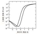
강유전체 결정화 어닐링을 행한 후의 실시예에 대하여 단면투과 전자현미경(단면 TEM) 분석을 행하고, SiO2를 주성분으로 하는 계면층(5)을 3.4nm보다 얇게 하는 것이 가능해졌다. 도 5에 개시하는 실시예 02B에서는, SiO2를 주성분으로 하는 계면층(5)의 두께는 2.6nm이었다. 도 5 중의 IL로 표기한 층이 계면층(5)이다. 이 실시예의 FeFET는 75nm 두께의 Ir, 135nm 두께의 x=0.2의 CSBT, 4nm 두께의 HfO2가 Si의 반도체 기체 상에 형성되어 있다. x=0.2의 CSBT는 강유전체의 주성분이 x=0.2의 CaxSr1 - xBi2Ta2O9인 것을 의미하고 있다. 이러한 게이트 적층을 Ir(75nm)/CSBT(x=0.2,135nm)/HfO2(4nm)/Si로 약칭한다. 이하, 혼란이 없는 범위에서 그 약칭은 적절히 사용한다. n채널의 FeFET이고, 드레인 전류와 게이트 전압(Id-Vg)의 관계를 도 6의 (a)에 개시한다. 드레인 전류는 로그로 표현하고 있다. 이러한 FeFET의 게이트 길이(L)는 10㎛, 게이트 폭은 200㎛이다. Vg의 소인의 중심 Vc는 Vc=0V이다. 소인진폭 Vamp는 Vamp=3.3V이다. Vg의 소인범위는 Vc-Vamp=-3.3V에서 Vc+Vamp=3.3V이고, Vg는 -3.3V와 3.3V의 사이를 왕복 소인하였다. 이후 제로가 아닌 Vc로 측정하는 실시예도 있지만, 이온주입기술 등을 이용하여 반도체측의 불순물의 종류와 농도를 적절히 선택함으로써 Vc=0V는 실현할 수 있다. 한편, 소인진폭 Vamp는, 즉 FeFET로의 데이터의 입력 전압의 절대치이다. 이후 Id-Vg의 측정에서는 소인범위를 Vc±Vamp로 표기하는 경우가 있는데, Vc-Vamp와 Vc+Vamp의 사이, Vg를 왕복소인하였다는 의미이다. 도면에 기재한 화살표의 방향을 따라서 드레인 전류가 변화하였다. 드레인 전류(Id)는, 이 도면에서는 게이트 폭 1㎛당 전류로 규격화되어 있다. 이러한 Id-Vg의 관계를 얻었을 때의 드레인 전압(Vd), 소스 전압(Vs), 기판 전압(Vsub)의 조건은, Vd=0.1V, Vs=Vsub=0V이었다. 이하, 특별히 한정되지 않는 한, 다른 실시예에서도 이 Vd, Vs, Vsub의 전압 조건에서 Id-Vg의 관계를 측정하였다. 임계값 전압을 Id=1×10⁻⁸A/㎛에 대응한 게이트 전압으로 정의하면, 도 6의 (a)에서는 점 a와 점 b에 있어서의 게이트 전압 Va와 Vb이다. 그 차이를 메모리 윈도우 Vw로 정의하면, Vw=Va-Vb는 이 실시예에서는, Vw=0.59V이고, 선행기술에 따른 메모리 윈도우(도 30)에 비하여 충분히 넓다. 도 6의 (b)에, 소인진폭 Vamp와 메모리 윈도우의 관계를 나타낸다. 도면에 나타내는 바와 같이, Vamp=2.7V에서 Vw=0.40V, Vamp=3.6V에서 Vw=0.69V, Vamp=3.9V에서 Vw=0.79V이었다. 도 30의 (d)에 나타난 종래기술과 비교하여 메모리 윈도우는 각별히 넓어졌다. 특히 Vamp=2.7V라고 하는 작은 입력으로도 Vw=0.40V이다. 이와 같이 명확한 개선이 보인 주된 이유는 계면층의 두께가 2.6nm까지 저감된 것에 의하여 입력시에 계면층에 가해지는 전압이 낮아져, 보다 작은 입력 전압에서 전기분극 반전이 시작되게 되었기 때문이다.A cross-section transmission electron microscope (cross-sectional TEM) analysis was performed on the embodiment after the ferroelectric crystallization annealing, and it became possible to make the
도 7에 개시하는 실시예 21C에서는, 단면 TEM 분석으로부터 SiO2를 주성분으로 하는 계면층(5)의 두께는 2.5nm이었다. 이러한 실시예에서는, 반도체 기체(1)는, 완충 불화수소산으로 표면의 산화막을 제거한 후에, 감압환경 하에서 실리콘 표면을 1.4nm 산질화한 것으로, SiON(1.4nm)/Si로 약칭할 수 있다. 이러한 실시예의 적층은, 금속이 150nm 두께의 Ir, 강유전체가 x=0.2의 CSBT, 절연체가 6nm 두께의 HfO2로 구성되어 있다. 도 7에 개시하는 바와 같이, 처음에 1.4nm 산질화한 층과 융합한 SiO2를 주성분으로 하는 계면층(5)이 형성되어 있다. 도 7 중의 IL로 표기한 층이 계면층(5)이다. 이러한 계면층(5)의 두께는 2.5nm로, 3.4nm에 비하여 충분히 얇다.In Example 21C shown in Fig. 7, the thickness of the
실시예 02A는, 실시형태 1의 실시예이다. 게이트 적층의 구조는 Ir(75nm)/CSBT(x=0.2,135nm)/HfO2(4nm)/Si이다. 반도체 기체는 p형 Si이다. 금속과 반도체 기체 사이의 게이트 전압에 대한 전기용량(Cg-Vg)의 관계를 측정하고, 도 8을 얻었다. 금속 Ir의 평면 형상은 한 변 100㎛의 정사각형이다. 게이트 전압(Vg)을 -3.3V에서 +3.3V까지 상승시킨 후, -3.3V까지 복귀시켰다. 교류전압의 진폭은 0.1V, 교류주파수는 100kHz이었다. 도면으로부터 알 수 있듯이 Cg-Vg로부터 평가되는 메모리 윈도우 Vw는 0.56V이었다. Vw는 Cg=100nF/cm2에 있어서의 게이트 전압으로 평가하였다.Example 02A is an example of the first embodiment. The structure of the gate stacked structure is Ir (75 nm) / CSBT (x = 0.2, 135 nm) / HfO 2 (4 nm) / Si. The semiconductor substrate is p-type Si. The relationship between the capacitance (C g -V g ) against the gate voltage between the metal and the semiconductor substrate was measured, and FIG. 8 was obtained. The planar shape of the metal Ir is a square of 100 占 퐉 on one side. The gate voltage (V g ) was raised from -3.3 V to +3.3 V and then returned to -3.3 V. The amplitude of the AC voltage was 0.1 V, and the AC frequency was 100 kHz. As it can be seen from the figure memory window that evaluates from C g V g -V w was 0.56V. V w was evaluated by the gate voltage at Cg = 100 nF / cm 2 .
적층형성의 상세를 설명한다.Details of lamination formation will be described.
[반도체 기체(1)][Semiconductor substrate (1)]
반도체 기체(1)는 실리콘 혹은 실리콘을 성분으로 하여 가지는 반도체이다. Si와 Ge의 결정이어도 SiC여도 좋다. 반도체 기판 대신에 SOI(silicon on insulator) 기판을 사용하여도 좋다. 절연체(2)를 부착하기 전에는, 반도체 기체는, 표면의 산화막을 제거하는 것이 중요하다. 표면의 산화막을 제거한 후에 직접 절연체(2)의 형성공정을 행하든지, 또는 반도체 기체 표면을 질화 또는 산질화한 후에 절연체(2)의 형성공정을 행한다. 형성된 질화 또는 산질화의 바람직한 두께는 1.5nm 이내이다. 제조방법은 어떠한 방법이어도 상관없다. 예를 들어, 표면산화물은 불산용액, 완충불산용액에 침지하여 제거한다. 질화막은, 예를 들어 감압분위기 중에서 NH3 가스를 도입하여 고속 어닐링(RTA)을 행함으로써 형성된다. 산질화는, 예를 들어 감압분위기 중에서 O2 가스를 도입하여 고속 어닐링(RTA)을 행한 후에 감압분위기 중에서 NH3 가스를 도입하여 고속 어닐링(RTA)을 행함으로써 형성된다.The
[절연체(2)][Insulator (2)]
절연체(2)는, 치밀하고 게이트와 반도체 기체 표면 사이의 누설전류가 작은 것이 요청된다. 또한, FeFET의 제조공정으로 막(3a), 강유전체(3), 반도체 기체(1)와 원소의 상호확산이나 화학반응물을 만들지 않을 것도 요청된다. 더욱이, FeFET에 가한 게이트 전압이 유효하게 강유전체(3)에 가해지도록 절연체(2)는 유전율이 큰 것이 바람직하다. 더욱이는, 절연체(2)의 전자친화력(진공준위와 전도대의 최하단의 에너지의 차이)이 강유전체(3)의 전자친화력보다 작고, 더욱이는 절연체(2)의 이온화 포텐셜(진공준위와 가전자대 최상단의 에너지의 차이)이 강유전체(3)의 이온화 포텐셜보다 큰 것이 바람직하다. 혹시 절연체(2)의 전자친화력이 강유전체(3)의 전자친화력보다 크면 반도체 기체 표면의 SiO2를 주성분으로 하는 계면층(5)과 강유전체(3) 사이에서 절연체(2)가 도전성 전자의 우물이 되어, 누설전류 등으로 일단 우물에 들어간 전자는 빠져나오기 어려워 들어온 전자의 집합소가 된다. 절연체(2)에 전자가 존재하여 변동하면 FeFET 임계값 전압이 강유전체의 분극의 스위치와는 다른 기구로 시프트되어 버린다. 혹시 절연체(2)의 이온화 포텐셜이 강유전체(3)의 이온화 포텐셜보다 작으면, 반도체 기체 표면의 SiO2를 주성분으로 하는 계면층(5)과 강유전체(3)의 사이에서 절연체(2)가 도전성 정공의 우물이 되어, 누설전류 등으로 일단 우물에 들어간 정공은 빠져나오기 어려워 들어온 정공의 집합소가 된다. 절연체(2)에 정공이 존재하여 변동하면 FeFET 임계값 전압이 강유전체의 분극의 스위치와는 다른 기구로 시프트되어 버린다. 한편, Si로부터 본 SiO2의 장벽 높이는 전자 쪽이 정공보다 작아 반도체 기체(1)로부터 절연체(2)로의 전하의 주입은 전자 쪽이 일어나기 쉬우므로, 절연체(2)의 이온화 포텐셜이 강유전체(3)의 이온화 포텐셜보다 큰 것보다, 절연체(2)의 전자친화력이 강유전체(3)의 전자친화력보다 작은 것이 우선적으로 바람직하다. 절연체(2)에 대한 이러한 요건을 만족하면 절연체의 종류는 상관 없지만, 예를 들어 하프늄, 지르코늄, 란탄, 이트륨, 알루미늄, 마그네슘, 망간 등 원소의 단독산화물, 및 그들 원소의 혼합산화물과 그들의 적층산화물이 적합하다. 나열한 산화물에 질소를 첨가하는 것도 특히 누설전류를 줄이는 목적으로 유용하다. 알루미늄 질화물, 하프늄 질화물, 알루미늄과 하프늄 혼합질화물은 강유전체 결정화 어닐링시에 산소의 확산을 저하시켜 SiO2를 주성분으로 하는 계면층(5)의 형성을 적게 하는 작용이 있으므로 절연체(2)로서 적합하다. 알류미늄 질화물, 하프늄 질화물, 알루미늄과 하프늄의 혼합질화물 등의 질화물과 상기 절연체(2)에 대한 상기 요건을 만족하는 절연체인 산화물과의 복합화합물, 적층물도 적합하다. 덧붙이자면, 강유전체 결정화 어닐링 전에는 절연체가 아니어도 어닐링 후에 상기 요건을 만족하는 강유전체(2)를 형성하면 된다.The
상기한 바와 같이 SiO2를 주성분으로 하는 계면층(5)은 3.4nm보다 얇게 하는 것이 바람직하므로, 절연체(2)의 SiO2 환산 막두께(EOT)도 3.4nm보다 얇고, 0.2nm 이상 2nm 이하로 제한하는 것이 동일한 정도의 전압이 계면층(5)과 절연체(2)에 가해져 바람직하다. 절연체(2)의 비유전율을 kin, SiO2의 비유전율을 ksio2로 표기하면, 절연체(2)의 실제 막두께 di는 di=(kin/ksio2)*EOT이고, 절연체(2)가 HfO2인 경우, kin=25, ksio2=3.9를 이용하면, EOT가 0.2nm 이상 2nm 이하에 대응한 HfO2의 실제 막두께는 1.3nm 이상 13nm 이하이다.As described above, it is preferable to make the
절연체(2)는, 상기 요건을 만족하는 것이라면 어떠한 제작법으로 형성하여도 좋다. 펄스 레이저 퇴적법, 스퍼터링법, 유기금속 화학기상 퇴적법, 원자층 퇴적법 등의 방법을 이용하여 적절히 절연체(2)를 형성한다.The
[막(3a)][Film (3a)]
3a는, Bi 층상 페로브스카이의 구성 원소로 구성되는 막이다. 결정화 어닐링 전이므로 Bi 층상 페로브스카이 결정 구조로 되어 있지는 않다. 대표적인 것은 스트론튬과 비스무트와 탄탈과 산소의 원소로 구성되는 막, 칼슘과 스트론튬과 비스무트와 탄탈과 산소의 막, 스트론튬과 비스무트와 탄탈과 니오브와 산소의 막, 칼슘과 스트론튬과 비스무트와 탄탈과 니오브와 산소의 막이다. 비스무트와 티탄과 산소의 막, 비스무트와 란탄과 티탄과 산소의 막, 비스무트와 네오디늄과 티탄과 산소의 막이어도 좋다.3a is a film composed of constituent elements of Bi layered perovskite. Since it is before the crystallization annealing, it does not have a Bi layered perovskite crystal structure. Typical examples are films consisting of strontium, bismuth, tantalum and oxygen, calcium, strontium and bismuth, tantalum and oxygen, strontium and bismuth, tantalum and niobium and oxygen, calcium and strontium, bismuth, tantalum and niobium It is a film of oxygen. Films of bismuth, titanium and oxygen, films of bismuth and lanthanum and titanium and oxygen, films of bismuth and neodymium, and titanium and oxygen.
막(3a)은, 펄스 레이저 퇴적법, 스퍼터링법, 유기금속 화학기상 퇴적법, 유기금속분해(MOD)법, 졸·겔법 등으로 형성된다.The
[금속(4)][Metal (4)]
금속(4)으로서, 순수한 금속 및 그 합금, 도전성 산화물이 선택된다. 막(3a) 상에 금속(4)을 형성하고나서 강유전체 결정화 어닐링을 하면, 데이터 보유 특성이나 데이터 리라이팅 내성이 뛰어난 FeFET가 생긴다. 강유전체 결정화 어닐링의 온도는 700℃~820℃, 시간은 10분~60분이 바람직하므로, 이러한 어닐링 조건에 견디는 재료인 것이 요청된다. 예의 검토의 결과, Ir, Pt, Ir과 Pt의 합금, 및 Ru가 적합한 것을 알 수 있었다.As the metal (4), pure metals and alloys thereof, and conductive oxides are selected. When the
금속(4)의 형성법에 한정은 없지만, 예를 들어 스퍼터링법, 유기금속 화학기상 퇴적법, 전자빔 증착법으로 형성된다.The method for forming the
[강유전체 결정화 어닐링][Ferroelectric crystallization annealing]
금속(4)까지 형성한 후에, 강유전체 결정화 어닐링을 적합한 온도환경에서 행한다. 이에 따라, 막(3a)은 강유전체(3)로 변화한다. 강유전체(3)는 강유전체 분극 반전피로에 강한 Bi 층상 페로브스카이트를 주성분으로 하는 재료로 구성한다. 상기의 막(3a)의 원소조성에 따라서 주성분은 SrBi2Ta2O9, SrBi2Ta2O9의 Sr의 일부를 Ca로 치환한 CaxSr1 - xBi2Ta2O9, SrBi2Ta2O9과 CaxSr1 - xBi2Ta2O9의 Ta의 일부를 Nb로 치환한 것, 및 Bi4Ti3O12, (Bi,La)4Ti3O12, (Bi,Nd)4Ti3O12이 된다. 금속(4)까지 형성한 후에 어닐링을 행하면 좋은 것은, 어닐링의 결과로서 강유전체(3)와 금속(4)의 계면 부근의 성질이 안정화되기 때문으로 생각하고 있다. 이것은 뛰어난 데이터 보유 특성, 뛰어난 리라이팅 내성으로 이어진다. 예의 검토를 거듭하여, 강유전체 결정화 어닐링은, N2나 Ar 등의 비활성 가스에 산소를 혼합한 가스환경에서 행하는 것이 매우 중요한 것을 알 수 있었다. 강유전체 결정화 어닐링 후의 강유전체(3)가 Bi 층상 페로브스카이트 결정구조를 가지는 것을 X선 회절법으로 확인하였다. 강유전체 막두께는 상기한 바와 같이 59nm<df<150nm인 것이 적합하다. 더욱 상세하게 설명하면, SiO2를 주성분으로 하는 계면층(5)의 형성을 작게 하기 위하여는, 강유전체 결정화 어닐링시에 분위기 가스의 성분은 산소를 최대한 줄여 질소나 아르곤을 주성분으로 하는 것이 중요하다. 동시에, 막(3a)을 Bi 층상 페로브스카이트의 강유전체로 변화시키기 위해서는, 강유전체가 산화물이므로, 분위기 가스 중에 어느 정도 산소가 존재하는 것도 요청된다. 더욱이, 금속(4)이 이러한 어닐링에 견디는 것도 필요하며, 선택한 Ir, Pt, Ir과 Pt의 합금, 및 Ru에서 각각 적합한 산소 가스양이 존재한다.After forming up to the
상기 적층형성의 상세를 실시예를 통하여 개시해 간다. 실시예 26C에서는, 절연체(2)는 하프늄과 란탄과 알루미늄의 복합산화물(Hf-La-Al-O)로, 구성 몰비는 HfO2:LaAlO3=7:3이다. 게이트 적층의 구조와 두께는, Ir(75nm)/CSBT(x=0.2,135nm)/Hf-La-Al-O(5nm)/Si이다. N2에 산소를 혼합한 분위기(N2와 O2의 체적비가 1:0.001) 중, 760℃에서 30분간 강유전체 결정화 어닐링을 행하였다. 도 9가 Id-Vg의 측정결과이고, 게이트 전압의 소인범위 ±3.3V에서 메모리 윈도우 Vw=0.48V이었다. 실시예 16A에서는, 절연체(2)는 지르코늄과 이트륨의 복합산화물(Zr-Y-O)로, 구성 몰비는 ZrO2:Y2O3=92:8이다. 게이트 적층의 구조와 두께는, Ir(75nm)/CSBT(x=0.25,135nm)/Zr-Y-O(5nm)/Si이다. N2에 산소를 혼합한 분위기(N2와 O2의 적층비가 1:0.001) 중, 760℃에서 30분간 강유전체 결정화 어닐링을 행하였다. 도 10이 Id-Vg의 측정결과이며, 게이트 전압의 소인범위 ±3.3V에서 메모리 윈도우 Vw=0.37V이었다. 실시예 302B에서는, 절연체(2)는 HfO2이다. 게이트 적층의 구조와 두께는, Ir(75nm)/CSBT(x=0.2,135nm)/HfO2(4nm)/Si이다. N2에 산소를 혼합한 분위기(N2와 O2의 체적비가 1:0.001) 중, 750℃에서 30분간 강유전체 결정화 어닐링을 행하였다. 도 11이 Id-Vg의 측정결과이고, 게이트 전압의 소인범위 0.5V±3.3V에서 메모리 윈도우 Vw=0.64V이었다. 실시예 20C에서는, 강유전체는 Nb를 포함한다. 게이트 적층의 구조와 두께는, Ir(75nm)/Ca0 . 2Sr0 . 8Bi2(Ta0.75Nb0.25)2O9(135nm)/HfO2(5nm)/Si이다. N2에 산소를 혼합한 분위기 중, 793℃에서 30분간 강유전체 결정화 어닐링을 행하였다. 게이트 전압의 소인범위 0V±3.3V에서 메모리 윈도우 Vw=0.28V이었다.Details of the lamination formation will be described through examples. In Example 26C, the
실시예 12B에서는, 절연체(2)는 Si 상에 질화하프늄 2nm와 그 위에 HfO2를 4nm 퇴적한 적층막으로, 게이트 적층의 구조와 두께는, Ir(75nm)/CSBT(x=0.2,135nm)/HfO2(4nm)/Hf-N(2nm)/Si이다. N2에 산소를 혼합한 분위기(N2와 O2의 체적비가 1:0.001) 중, 780℃에서 30분간 강유전체 결정화 어닐링을 행하였다. 도 12가 Id-Vg의 측정결과이며, 게이트 전압의 소인범위 0.5V±3.3V에서 메모리 윈도우 Vw=0.57V이었다. 실시예 25C에서는, 절연체(2)는 Si 상에 질화알루미늄 2nm와 그 위에 HfO2를 4nm 퇴적한 적층막으로, 게이트 적층의 구조와 두께는, Ir(75nm)/CSBT(x=0.2,135nm)/HfO2(4nm)/Al-N(2nm)/Si이다. N2에 산소를 혼합한 분위기(N2와 O2의 체적비가 1:0.001) 중, 780℃에서 30분간 강유전체 결정화 어닐링을 행하였다. Id-Vg를 측정한 결과, 게이트 전압의 소인범위 1.8V±3.3V에서 메모리 윈도우 Vw=0.52V이었다. 실시예 18C에서는, 절연체(2)는 질화하프늄 5nm에서, 게이트 적층의 구조와 두께는, Ir(75nm)/CSBT(x=0.2,135nm)/Hf-N(5nm)/Si이다. N2에 산소를 혼합한 분위기(N2와 O2의 체적비가 1:0.0006) 중, 750℃에서 30분간 강유전체 결정화 어닐링을 행하였다. Id-Vg를 측정한 결과, 게이트 전압의 소인범위 ±3.3V에서 메모리 윈도우 Vw=0.39V이었다. 실시예 402A에서는, x=0.3의 CSBT를 이용한 실시예이고, 게이트 적층의 구조와 두께는, Ir(75nm)/CSBT(x=0.3,135nm)/HfO2(5nm)/Si이다. N2에 산소를 혼합한 분위기 중, 793℃에서 30분간 강유전체 결정화 어닐링을 행하였다. Id-Vg를 측정한 결과, 게이트 전압의 소인범위 ±3.3V에서 메모리 윈도우 Vw=0.42V이었다. In Example 12B, the
실시예 12B와 마찬가지로, 절연체(2)가 Si 상에 질화하프늄(Hf-N)과 그 위에 HfO2를 퇴적한 적층에 의하여 형성된 실시예의 결과를 표 1에 정리하였다. 게이트 적층의 구조는 공통적으로 Ir/CSBT(x=0.2)/HfO2/Hf-N/Si이다. Id-Vg 특성의 메모리 윈도우는 게이트 전압의 소인범위가 VC±3.3V일 때의 값이다. Hf-N은 유기금속 화학기상 퇴적(MOCVD)법에 의하여 형성하였다. 각각의 실시예에 대하여 MOCVD법의 키가 되는 제조조건을 표 1에 나타내었다. NH3 유량은 9sccm 이상 20sccm 이하가 적합하고, 이 범위로 함으로써 0.4V 이상의 메모리 윈도우를 얻었다. 또한, 서셉터 온도는 260℃ 이상 400℃ 이하가 적합하다. Hf-N의 두께는 1nm 이상 2nm 이하로 하였다. 단면 TEM 분석의 결과, 실시예 11A의 SiO2를 주성분으로 하는 계면층의 두께는 3.1nm이었다.As in Example 12B, the results of Examples in which the
상기 실시예 02B, 21C, 02A, 26C, 16A, 302B, 12B에 있어서, 금속(4)의 Ir은 스퍼터링법으로, 막(3a)은 펄스 레이저 퇴적법으로 형성하고, 절연체(2)에 대하여는, 질화하프늄과 질화알루미늄은 유기금속 화학기상 퇴적법으로, 그 이외의 재료는 펄스 레이저 퇴적법으로 형성하였다. 실시예 09F에서는, 막(3a)를 유기금속 화학기상 퇴적법으로 퇴적하였다. 강유전체(3)의 CSBT의 두께는 120nm, Ca의 조성 x는 x=0.15이었다. 게이트 적층의 구조와 두께는, Ir(75nm)/CSBT(x=0.15,120nm)/HfO2(5nm)/Si이다. N2에 산소를 혼합한 분위기(N2와 O2의 체적비가 1:0.00026) 중, 780℃에서 30분간 강유전체 결정화 어닐링을 행하였다. 도 13이 Id-Vg의 측정 결과이고, 게이트 전압의 소인범위 0.5V±3.3V에서 메모리 윈도우 Vw=0.51V이었다. 실시예 09F에서는, Ir은 스퍼터링법, HfO2는 펄스 레이저 퇴적법으로 형성하였다.Ir of the
비활성 가스 Ar에 산소를 혼합한 분위기에서 강유전체 결정화 어닐링을 행하여도 좋다. 실시예 03C에서는, 절연체(2)는 하프늄과 마그네슘의 복합산화물(Hf-Mg-O)로, 구성 몰비는 HfO2:MgO=7:3이다. 게이트 적층의 구조와 두께는, Ir(75nm)/CSBT(x=0.2,135nm)/Hf-Mg-O(5nm)/Si이다. Ar에 산소를 혼합한 분위기(Ar과 O2의 체적비가 1:0.001) 중, 760℃에서 30분간 강유전체 결정화 어닐링을 행하였다. 도 14가 Id-Vg의 측정 결과이며, 게이트 전압의 소인범위 ±3.3V에서 메모리 윈도우 Vw=0.44V이었다.The ferroelectric crystallization annealing may be performed in an atmosphere in which oxygen is mixed with the inert gas Ar. In Example 03C, the
강유전체 결정화 어닐링에 관하여, 질소가스 N2에 산소 가스 O2를 혼합한 분위기, 온도, 압력에 관하여 상세하게 검토하였다. 우선은, 금속(4)으로서 Ir을 이용한 경우, 도 15는 혼합가스 중의 N2와 O2의 체적비율 y와 그 체적비율을 이용하여 제조하여 측정한 FeFET의 Id-Vg 특성의 메모리 윈도우와의 관계를 개시하고 있다. 세로축의 변수인 메모리 윈도우는 게이트 전압의 소인범위가 Vc±3.3V일 때의 값이다. 가로축의 변수 y는 N2의 체적에 대한 O2의 체적의 비율, 즉 y=[혼합가스 중의 O2의 체적]/[혼합가스 중의 N2의 체적]이다. 도 15 중의 마크 1개 1개가 제작한 FeFET의 실시예로 되어 있다. 도 15 중의 실시예 모두에 공통적으로, 게이트 적층의 구조와 두께는, Ir(75nm)/CSBT(x=0.2,135nm)/HfO2(4nm)/Si이고, 강유전체 결정화 어닐링의 온도와 시간은 780℃, 30분이다. Ir은 스퍼터링법으로, CSBT와 HfO2는 펄스 레이저 퇴적법으로 형성하였다. 강유전체 결정화 어닐링의 혼합가스비는, 어닐링 용기를 일단 진공으로 배기한 후에 소정의 조건으로 정리하였다. 도 15 중의 (▲)마크의 실시예는, 어닐링 중에 질소가스와 산소 가스의 흐름이 있는 경우이고, 보다 구체적으로는 N2 유량이 1000sccm, O2 유량은 1000y sccm이었다. (■)마크의 실시예는 어닐링 중에 질소가스와 산소 가스의 흐름이 없는 경우이다. 양호한 메모리 윈도우를 얻기 위한 좋은 조건은, 가스의 흐름의 유무에 상관없이, 가스 체적비율 y로 나타나는 것을 알 수 있었다. Ir을 금속(4)으로 선택한 경우에는, 산소의 체적비율 y의 적합한 조건은 0.0002 이상, 0.02 이하이고, 메모리 윈도우 0.4V 이상을 얻었다.Regarding the ferroelectric crystallization annealing, the atmosphere, the temperature and the pressure in which the nitrogen gas N 2 and the oxygen gas O 2 are mixed are examined in detail. First, when Ir is used as the metal (4), Fig. 15 is a graph showing the I d -V g characteristics of the FeFET measured and produced by using the volume ratio y and the volume ratio of N 2 and O 2 in the mixed gas. And the like. The memory window, which is a variable in the vertical axis, is a value when the sweep range of the gate voltage is V c ± 3.3V. The variable y on the horizontal axis is the ratio of the volume of O 2 to the volume of N 2 , that is, y = [volume of O 2 in the mixed gas] / [volume of N 2 in the mixed gas]. One of the marks in Fig. 15 is an embodiment of the FeFET produced. 15, the structure and the thickness of the gate stack are Ir (75 nm) / CSBT (x = 0.2, 135 nm) / HfO 2 (4 nm) / Si and the temperature and time of the ferroelectric crystallization annealing are 780 Lt; 0 > C, 30 minutes. Ir was formed by sputtering, and CSBT and HfO 2 were formed by pulsed laser deposition. The mixed gas ratio of the ferroelectric crystallization annealing is summarized under predetermined conditions after evacuating the annealing vessel once by vacuum. An example of the mark () in Fig. 15 is a case where there is a flow of nitrogen gas and oxygen gas during annealing, more specifically, an N 2 flow rate is 1000 sccm and an O 2 flow rate is 1000 y sccm. (1) marks are cases where there is no flow of nitrogen gas and oxygen gas during the annealing. It has been found that a good condition for obtaining a good memory window is represented by the gas volume ratio y regardless of the presence or absence of gas flow. When Ir is selected as the metal (4), a suitable condition of the volume ratio y of oxygen is 0.0002 or more and 0.02 or less, and a memory window of 0.4V or more is obtained.
다른 Ca 조성 x로 제작한 실시예에서도 가스의 흐름의 유무에 관계없이, 양호한 메모리 윈도우를 나타내었다. 실시예 24A에서는, x=0.25이고, 게이트 적층은 Ir(75nm)/CSBT(x=0.25,135nm)/HfO2(4nm)/Si이다. 가스 흐름 없음, y=0.001, 780℃, 30분의 조건으로 강유전체 결정 어닐링을 행하고, 게이트 전압의 소인범위 ±3.3V에서 메모리 윈도우는 0.51V이었다. 실시예 24B에서는, x=0.25이고, 게이트 적층은 Ir(75nm)/CSBT(x=0.25,135nm)/HfO2(4nm)/Si이다. 가스 흐름이 있음, y=0.001, 780℃, 30분의 조건에서 강유전체 결정 어닐링을 행하고, 게이트 전압의 소인범위 ±3.3V에서 메모리 윈도우는 0.53V이었다. 실시예 27A에서는, x=0.1이고, 게이트 적층은 Ir(75nm)/CBST(x=0.1,135nm)/HfO2(4nm)/Si이다. 가스 흐름 없음, y=0.001, 780℃, 30분의 조건에서 강유전체 결정 어닐링을 행하고, 게이트 전압의 소인범위 ±3.3V에서 메모리 윈도우는 0.48V이었다. Even in the case of the other Ca composition x, a good memory window was shown regardless of the flow of the gas. In Example 24A, x = 0.25 and the gate stack is Ir (75 nm) / CSBT (x = 0.25, 135 nm) / HfO 2 (4 nm) / Si. Ferroelectric crystal annealing was performed under the condition of no gas flow, y = 0.001, 780 캜 for 30 minutes, and the memory window was 0.51 V at the sweep range of the gate voltage of +3.3 V. In Example 24B, x = 0.25 and the gate stack is Ir (75 nm) / CSBT (x = 0.25, 135 nm) / HfO 2 (4 nm) / Si. The ferroelectric crystal annealing was performed under the condition of the gas flow, y = 0.001, 780 캜 for 30 minutes, and the memory window was 0.53 V at the sweep range of the gate voltage of 3.3 V. In Example 27A, x = 0.1 and the gate stack is Ir (75 nm) / CBST (x = 0.1, 135 nm) / HfO 2 (4 nm) / Si. Ferroelectric crystal annealing was performed under the conditions of no gas flow, y = 0.001, 780 캜 for 30 minutes, and the memory window was 0.48 V at a sweep range of the gate voltage of 3.3 V.
도 16은 강유전체 결정화 어닐링 공정에 있어서의 어닐링 온도와 제조한 FeFET의 Id-Vg 특성의 메모리 윈도우의 관계를 개시하고 있다. 세로축의 변수인 메모리 윈도우는 게이트 전압의 소인범위가 Vc±3.3V일 때의 값이다. 어닐링 시간은 30분이다. 도 16 중의 마크 1개 1개가 제작한 FeFET의 실시예로 되어 있다. (▲)마크의 실시예는, 어닐링 중에 질소가스와 산소 가스의 흐름이 있는 경우이고, 보다 구체적으로는 N2 유량이 1000sccm, O2 유량은 1sccm이었다. (■)마크의 실시예는 어닐링 중에 질소가스와 산소 가스의 흐름이 없는 경우이다. (▲)마크의 실시예에서는, 게이트 적층의 구조와 두께는 Ir(75nm)/CSBT(x=0.2,135nm)/HfO2(5nm)/Si이고, (■)마크의 실시예에서는, 게이트 적층의 구조와 두께는, Ir(75nm)/CSBT(x=0.2,135nm)/HfO2(4nm)/Si이다. 강유전체 결정화 어닐링을 위한 적합한 온도조건은 730℃ 이상 800℃ 이하이고, 메모리 윈도우 04V 이상을 얻었다.16 discloses the relationship between the annealing temperature in the ferroelectric crystallization annealing process and the memory window of the I d -V g characteristics of the fabricated FeFET. The memory window, which is a variable in the vertical axis, is a value when the sweep range of the gate voltage is V c ± 3.3V. The annealing time is 30 minutes. One of the marks in Fig. 16 is one embodiment of the FeFET produced. (▴) mark shows a case where there is a flow of nitrogen gas and oxygen gas during annealing, more specifically, the flow rate of N 2 is 1000 sccm and the flow rate of O 2 is 1 sccm. (1) marks are cases where there is no flow of nitrogen gas and oxygen gas during the annealing. The structure and thickness of the gate stacked structure are Ir (75 nm) / CSBT (x = 0.2, 135 nm) / HfO 2 (5 nm) / Si, The structure and the thickness of Ir (75 nm) / CSBT (x = 0.2, 135 nm) / HfO 2 (4 nm) / Si. Suitable temperature conditions for ferroelectric crystallization annealing were 730 ℃ ~ 800 ℃, and memory window was more than 04V.
금속(4)으로서 Ir 이외의 실시예를 표 4에 개시한다. 22A, 22B, 22C, 19E, 19B, 19C의 실시예에서는, Pt를 금속(4)으로서 이용하였다. 19E를 제외하고 메모리 윈도우는 0.40V 이상이었다. 강유전체 결정화 어닐링 시의 질소가스에 대한 산소 가스의 체적비율 y가 상기 6개의 실시예에서 다르다. 산소를 포함하지 않는 순수한 질소 중 700℃~800℃에서 어닐링하면 Pt가 박리된다. 산소의 함유가 적은, 즉 y가 적은 실시예에 주목하면, y=0.0003의 실시예 19E에서는, Id-Vg 특성은 취득할 수 있는데, Pt의 손상이 크다. y=0.0001의 실시예도 시도하였지만, Pt의 박리가 심하여 Id-Vg 측정은 불가능하였다. y=0.0007의 실시예 22C에서는, 거의 문제 없지만, FeSEM(전계방사형 주사형 전자현미경)의 관찰에서 Pt의 결함이 보이기 시작하고 있다. Pt에 의하여 금속(4)을 구성한 경우, y는 0.0007보다 크고 0.01 이하인 것이 바람직하다. Ir에서는, 순수한 질소 중 700℃~800℃ 어닐링에서 이와 같은 박리나 결함은 일어나지 않는다. 금속(4)으로서 Ir과 Pt의 중량비가 1:1의 Ir과 Pt의 합금을 스퍼터링법으로 형성한 실시예가 14A, 14B이다. y=0.0004의 실시예 14B에서는, 금속의 박리는 보이지 않았지만, y=0.0001의 실시예 14A에서는 금속의 결함이 아주 조금 관찰되었다. Ru를 금속(4)으로 하는 실시예가 17C이며, y=0.0005의 어닐링 조건에서 Ru의 결함은 관찰되지 않았다.Examples of the metal (4) other than Ir are shown in Table 4. In the examples of 22A, 22B, 22C, 19E, 19B and 19C, Pt was used as the
지금까지 개시한 실시예에서는, 강유전체 결정화 어닐링은 모두 1기압(1atm) 하에서 행하였다. 1atm보다 작은 감압환경에서의 강유전체 결정화 어닐링도 행하였다. 그 결과를 도 17 및 표 2와 표 3에 정리하였다. 도면의 마크 근방에 실시예명이 표기되어 있고, 그 실시예의 어닐링 조건의 상세는 표 2와 표3에서 확인할 수 있다. 12G, 12H, 12I, 12B, 16F의 실시예는, 질소와 산소의 혼합가스 중에서 행하여지고, 체적비율 y=0.001이다. 어닐링 시의 압력(전체압)은, 도 17 및 표 2로부터 판독할 수 있다. 도 17 및 표 2로부터 알 수 있듯이, 1atm 이하이고 0.001MPa 이상의 압력 조건은, 0.4V 이상의 메모리 윈도우를 얻기 위하여 적합하다.In the embodiments disclosed so far, the ferroelectric crystallization annealing is performed under all atmospheric pressure (1 atm). Ferroelectric crystallization annealing was also performed in a reduced pressure environment of less than 1 atm. The results are summarized in Fig. 17 and Table 2 and Table 3. The name of the embodiment is shown in the vicinity of the mark in the figure, and the details of the annealing condition of the embodiment are shown in Table 2 and Table 3. [ 12G, 12H, 12I, 12B, and 16F are performed in a mixed gas of nitrogen and oxygen, and the volume ratio y = 0.001. The pressure (total pressure) at the time of annealing can be read from Fig. 17 and Table 2. As can be seen from Fig. 17 and Table 2, a pressure condition of not more than 1 atm and not less than 0.001 MPa is suitable for obtaining a memory window of 0.4 V or more.
검토를 거듭해 왔지만, 강유전체 결정화 어닐링 시에 가스는 산소만으로 하여 압력을 낮추는 것도 유효한 것을 발견하였다. 도 17과 표 3에 기재한 12L, 12K의 실시예가 개시하는 바와 같이 도입가스가 산소만으로 압력이 10-5MPa(즉, 10Pa) 이상이고 10-4MPa(즉, 100Pa) 이하가, 0.4V 이상의 메모리 윈도우를 얻기 위하여 적합하다. 감압환경이므로 SiO2를 주성분으로 하는 계면층(5)의 형성을 작게 하고, 산화물인 강유전체의 어닐링에 필요한 산소도 공급하기 위하여, 적합한 어닐링 조건이 되었다고 사료된다.It has been found out that it is also effective to lower the pressure by using only oxygen as the gas at the time of ferroelectric crystallization annealing. As described in the examples of 12L and 12K shown in Fig. 17 and Table 3, when the introduction gas has a pressure of 10 -5 MPa (i.e. 10 Pa) or more and 10 -4 MPa (i.e., 100 Pa) Or more memory window. It is considered that the annealing condition becomes suitable for reducing the formation of the
도 18에는 절연체(2)에 HfO2를 채용한 경우의 HfO2의 두께와 메모리 윈도우의 관계가 개시된다. 도면 중의 1점 1점이 실시예에 대응한다. (■)마크는 가스의 흐름이 없는 경우, (▲)마크는 가스의 흐름이 있는 경우의 실시예이다. 게이트 적층의 구조와 두께는 Ir(75nm)/CSBT(x=0.25,135nm)/HfO2/Si이고, 산소 가스 체적비율은 y=0.001이었다. 도 18은 HfO2의 두께는 2nm 이상 6nm 이하가 매우 적합한 것을 나타내고 있다.Fig. 18 shows the relationship between the thickness of HfO 2 and the memory window when HfO 2 is used for the
상기한 모든 본 발명의 FeFET의 Id-Vg 특성을 특성 조정하기 위한 어닐링 공정을 2가지 발견하였다. 상기한 모든 공정을 끝낸 후에 이 특성 조정 어닐링을 행한다. 제1 방법은, 강유전체 결정화 어닐링보다 낮은 온도조건으로 산소 가스 중에서 행한다. 제2 방법은, 수소를 포함하는 가스 중에서 행한다. 양쪽의 특성 조정 어닐링을 병용하여도 좋다.There have been found two annealing processes for characterizing I d -V g characteristics of the FeFET of the present invention. After the above-described processes are completed, this characteristic adjustment annealing is performed. The first method is performed in an oxygen gas at a temperature lower than that of the ferroelectric crystallization annealing. The second method is performed in a gas containing hydrogen. Both of the characteristic adjusting annealing may be used in combination.
제1 방법에서는, 어닐링 온도는 500℃ 이상에서 700℃ 이하, 어닐링 시간은 10분 이상에서 60분 이하이면 좋다. 도 19는 실시에 02B의 칩 상의 하나의 FeFET의 특성 조정 어닐링 전후의 Id-Vg 특성을 개시하고 있다. 점선커브가 특성 조정 전, 실선커브가 특성 조정 후이다. 게이트 전압이 0V에서 1V 부근에서 게이트 전압의 변화에 대하여 특성 조정 어닐링 후에서는, 특성 조정 어닐링 전보다 명확히 가파르게 드레인 전류가 변화하고 있다. 일반적으로 좁은 전압변화에서 큰 전류변화가 있던 쪽이 좋다고 생각되므로, 특성이 개량되었다. 정량적으로는 SS(sub-threshold swing)값으로 평가된다. SS값은 전압 임계값보다 낮은 전압 부근에서, 드레인 전류를 1자릿수 변화시키는 데에 필요한 게이트 전압으로, SS값이 작은 편이 좋다. Id=10-10A/㎛에 있어서의 곡선의 기울기로부터 SS값을 구하였다. 좌우의 히스테리시스 곡선으로부터 얻은 SS값의 평균값을 여기에서는 채용하였다. 또한, Id=10-8A/㎛에서 메모리 윈도우는 평가하였다. 도 19에는, 특성 조정 어닐링 온도에 대한 어닐링 후의 특성 변화율을 개시하고 있다. (○)표시는 메모리 윈도우의 변화율, (■)표시는 S값의 변화율이다. 여기에서 변화율은 ([어닐링 후의 물리량]-[어닐링 전의 물리량])/[어닐링 전의 물리량]으로 퍼센트(%)로 표시하고 있다. 어닐링 후에 메모리 윈도우 변화율이 감소하는 것은 좋지 않으며, SS값이 감소하는 것은 좋은 것이다. 도 20이 나타내는 바와 같이 500℃에서 700℃의 범위 내에서 메모리 윈도우의 변화율은 적고, 한편 SS값은 온도 상승과 함께 SS값이 크게 감소한다. 500℃에서 550℃의 범위에서도 10% 정도의 SS값의 감소가 보인다. 온도를 너무 상승시키면 SiO2를 주성분으로 하는 계면층(5)의 성장을 촉진하여 메모리 윈도우가 감소하게 되므로, 제1 방법의 어닐링 온도의 상한이 정해진다. 산소 중에서의 어닐링에 의하면 SiO2를 주성분으로 하는 계면층(5)과 Si 계면의 결함이 회복된다고 생각된다.In the first method, the annealing temperature may be 500 ° C or more and 700 ° C or less, and the annealing time may be 10 minutes or more to 60 minutes or less. Fig. 19 discloses I d -V g characteristics before and after the characterization annealing of one FeFET on the chip of embodiment 02B. Before the characteristic adjustment of the dotted curve, the solid curve is after the characteristic adjustment. After the characteristic adjustment annealing with respect to the change of the gate voltage in the vicinity of the gate voltage of 0 V to 1 V, the drain current clearly changes more clearly than before the characteristic adjustment annealing. In general, it is considered that there is a large current change at a narrow voltage change, so the characteristics are improved. It is quantitatively evaluated as a sub-threshold swing (SS) value. The SS value is a gate voltage necessary for changing the drain current by one digit in the vicinity of the voltage lower than the voltage threshold value, and the SS value should be small. The SS value was obtained from the slope of the curve at I d = 10 -10 A / 占 퐉. The average value of the SS values obtained from the left and right hysteresis curves was adopted here. The memory window was also evaluated at I d = 10 -8 A / μm. Fig. 19 discloses the rate of characteristic change after annealing to the characteristic adjustment annealing temperature. (O) is the rate of change of the memory window, and (I) is the rate of change of the S value. Here, the rate of change is expressed in percent (%) as ([physical quantity after annealing] - [physical quantity before annealing]) / [physical quantity before annealing]. It is not good that the rate of change of the memory window after annealing decreases, and it is good that the SS value decreases. As shown in Fig. 20, the change rate of the memory window is small in the range of 500 deg. C to 700 deg. C, while the SS value greatly decreases in SS value with temperature rise. A decrease in the SS value of about 10% is seen even in the range of 500 ° C to 550 ° C. If the temperature is raised too much, the growth of the
제2 방법에서는, 수소 함유가 3% 내지 5%의 수소와 질소의 혼합가스를 이용한다. 어닐링 온도는 350℃ 이상 450℃ 이하, 어닐링 시간은 3분 이상 30분 이하의 조건이 바람직하다. 도 21과 도 22에 의하여 제2 방법의 명확한 효과를 볼 수 있다. 도 21은 상기 실시예 21C에 대하여 400℃에서 30분간 어닐링을 행하였다. 어닐링 후(실선커브)의 쪽이 어닐링 전(점선커브)에 비하여 게이트 전압의 변화에 대하여 명확히 가파르게 변화하고 있다. 도 22는, 23C의 실시예 칩 상의 하나의 FeFET에 대하여 제2 방법의 어닐링을 400℃에서 5분간 행한 결과를 나타내고 있다. 도 21과 마찬가지로 개량된 효과가 보인다. SiO2를 주성분으로 하는 계면층(5)과 Si의 계면의 단글링 본드(dangling bond)에 수소원자가 삽입 계면의 상태 밀도를 감소시키기 때문에, 수소 어닐링 효과는 나타났다고 생각된다. 고온 또는 장시간의 수소 어닐링은 산화물인 강유전체를 분해시키기 때문에, 상기 온도와 시간의 범위가 적합하다.In the second method, a mixed gas of hydrogen and nitrogen with a hydrogen content of 3% to 5% is used. The annealing temperature is preferably 350 占 폚 to 450 占 폚, and the annealing time is preferably 3 minutes to 30 minutes. 21 and 22, a clear effect of the second method can be seen. Fig. 21 shows the annealing of Example 21C at 400 DEG C for 30 minutes. The line after the annealing (solid line curve) clearly changes steeply with respect to the change of the gate voltage before annealing (dotted line curve). 22 shows the result of annealing the second method at 400 占 폚 for 5 minutes for one FeFET on the chip of Example 23C. An improved effect is shown as in Fig. It is considered that the hydrogen annealing effect appears because the hydrogen atoms reduce the state density of the interfacial interface in the
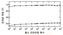
입력 전압의 절대치가 3.3V일 때의 펄스 리라이팅 내성 특성과 데이터 보유 특성을 개시한다.A pulse resilience resistance characteristic and a data retention characteristic when the absolute value of the input voltage is 3.3 V are disclosed.
실시예 02B의 FeFET를 이용하였다. 높이 -3.3V 폭 10μs의 음극성 펄스에 높이 3.3V 폭 10μs의 양극성 펄스를 계속한 주기 20μs의 교류 펄스를 1 주기(1 사이클)로 하였다. 이러한 리라이팅 교류 펄스를 반복 부여한다. 리라이팅 교류 펄스를 부여하고 있는 동안에는 Vd=Vs=Vsub=0V이다. 이러한 교류 펄스를 누적 소정의 횟수 부여한 후, 리라이팅 내성을 보기 위하여 Id-Vg 특성을 측정한다. 게이트 전압을 ±3.3V 왕복 소인한다. 게이트 전압 소인의 동안에는 Vd=0.1V, Vs=Vsub=0V이다. Id=10-8A/㎛를 부여하는 도 6의 (a)에서 설명하는 바와 같이 2개의 게이트 전압(임계값 전압)을 취득한다. 그 후, 교류 펄스를 다시 부여한다. 소정의 누적 횟수가 되면, 다시 리라이팅 내성을 보기 위하여 Id-Vg 특성을 측정한다. 이것을 반복한다. 이렇게 하여 도 23을 얻었다. (▼)표시의 임계값 전압은 게이트 전압을 -3.3V에서 3.3V로 상승시켰을 때에 얻어지는 임계값 전압치이고, (▲)표시의 임계값 전압은, 3.3V에서 -3.3V로 하강시켰을 때의 임계값 전압이다. 도 23으로부터 본 실시예는 109회 이상의 리라이팅 내성을 가진다. 특허문헌 1, 3, 비특허문헌 4, 5 등에 기재된 기술에 따르면, 종래기술은 108회 이상의 리라이팅 내성을 가진다. 도 23은, 본 발명의 FeFET도 동등 이상의 리라이팅 내성을 가지는 것을 나타내고 있다.The FeFET of Example 02B was used. The negative pulse of the height -3.3 V and the width of 10 mu s was subjected to the alternating pulse of 20 mu s for one period (one cycle) in which the bipolar pulse of the height 3.3
데이터 보유 특성에 대하여는, 높이 -3.3V 폭 0.1s의 음극성 펄스를 1개 부여한 후, 데이터 보유의 상태에 들어가 데이터 보유 동안 Vg=Vd=Vs=Vsub=0V이다. 도 24의 (▼)표시의 시점에서, 판독 동작을 행한다. 판독 동안 Vd=0.1V, Vs=Vsub=0V로 하고, Vg를 1.0V에서 0V로 소인하여 Id-Vg 특성을 얻고 Id=10-8A/㎛에 있어서의 Vg가 임계값 전압으로, 도 24에 플롯하였다. 소정의 시간 데이터 보유 후, 판독 동작을 행한다. 이것을 반복하여, 도면의 (▼)표시의 결과를 펄스 입력 후 105초까지 취득하였다. 높이 3.3V 폭 0.1s의 양극성 펄스를 1개 부여한 후, 데이터 보유 상태에 들어가, 동일한 판독 동작을 행한 결과를 (▲)표시로 나타내었다. 양호한 데이터 보유 특성을 나타내고 있다. 105초 후, 음극성 펄스 후의 임계값 전압은 양극성 펄스 후의 임계값 전압보다 약 0.31V 크다. 104초에서의 (▼)표시와 105초에서의 (▼)표시를 직선(점선)으로 연결하고, 그것을 10년까지 외삽하였다. 마찬가지로 104초에서의 (▲)표시와 105초에서의 (▲)표시를 직선(점선)으로 연결하고, 그것을 10년까지 외삽하였다. 이러한 외삽 조작은, 10년 후에도 임계값 전압의 차이가 약 0.18V 있어, 2가지의 기억 상태는 충분히 식별 가능한 것을 나타내고 있다. 이와 같이, 특허문헌 1 내지 3, 비특허문헌 1 내지 9 등에 기재된 데이터 보유 특성과 동등한 데이터 보유 특성을 본 발명은 가지고 있다. 한편, 데이터 보유 시간의 수명은 2가지 상태의 식별이 곤란해진 시간이다. 본 명세서에서는 임계값 전압의 차이가 0.05V에 이른 시간으로 정의한다. 한편, 판독시 게이트 전압을 고정하여 드레인 전류를 측정함으로써 데이터 보유 특성을 평가하는 방법도 있다. 이러한 경우, 온 전류의 오프 전류에 대한 비가 약 3인 것이, 상기 임계값 전압의 차이 0.05V에 거의 대응하므로, 데이터 보유 시간의 수명은 드레인 전류를 측정하는 방법에서는 온 전류의 오프 전류에 대한 비가 3에 도달한 시간으로 정의한다. 이러한 정의에 따르면 외삽이지만, 본 실시예의 데이터 보유 수명은 10년을 충분히 넘고 있다. 이와 같이 본 발명은, 종래 개발해 온 FeFET가 겸비하는 2가지 특성, 즉 105초 이상의 데이터 보유 특성과 108회 이상의 데이터 리라이팅 내성 특성의 한쪽도 손상시키지 않고, 입력 전압의 절대치가 3.3V 이하의 데이터 입력이 가능한 FeFET를 제공하고 있다.As for the data holding characteristic, one negative polarity pulse having a width of -3.3 V and a width of 0.1 s is applied, then enters a data holding state and V g = V d = V s = V sub = 0 V during data holding. At the time of () in FIG. 24, a read operation is performed. Reading for V d = 0.1V, V s = V sub = 0V to, and to sweep the V g from 1.0V to 0V gaining I d -V g characteristics I d = V g of 10 -8 in the A / ㎛ Is plotted in FIG. 24 as the threshold voltage. After holding the predetermined time data, a read operation is performed. This was repeated, and the result of the () mark in the drawing was acquired until 10 5 seconds after the pulse was input. One bipolar pulse having a height of 3.3 V and a width of 0.1 s is applied, and then the data holding state is entered and the same reading operation is performed. Indicating good data retention characteristics. After 10 5 seconds, the threshold voltage after the negative polarity pulse is about 0.31 V greater than the threshold voltage after the positive polarity pulse. The mark (?) At 10 4 seconds and the mark (▼) at 10 5 seconds are connected by a straight line (dotted line) and extrapolated to 10 years. Similarly, the (▲) mark at 10 4 seconds and the (▲) mark at 10 5 seconds are connected by a straight line (dotted line) and extrapolated to 10 years. This extrapolation operation shows that the difference in the threshold voltage is about 0.18 V even after 10 years, and that the two storage states can be sufficiently identified. Thus, the present invention has data holding characteristics equivalent to the data holding characteristics described in
본 발명의 FeFET는 입력 전압의 절대치가 3.3V를 넘는 경우도 양호한 소자 특성을 제공한다. 도 25와 도 26은 데이터 리라이팅 내성 시험의 결과이다. 도 25는 실시예 27E에 대한 결과이다. 실시예 27E의 게이트 적층과 두께는, Ir(75nm)/CSBT(x=0.2,135nm)/HfO2(5nm)/Si이고, 강유전체 결정화 어닐링은 질소에 대한 산소 체적비율 y=0.001의 혼합가스(1기압 가스 흐름 있음) 중에서 800℃, 30분 행하였다. 높이 -4.5V 폭 10μs의 음극성 펄스에 높이 4.5V 폭 10μs의 양극성 펄스를 계속한 주기 20μs의 교류 펄스를 1주기(1사이클)로 하였다. 이러한 리라이팅 교류 펄스를 반복 부여한다. 리라이팅 교류 펄스를 부여하고 있는 동안은 Vd=Vs=Vsub=0V이다. 이러한 교류 펄스를 누적 소정의 횟수 부여한 후, 판독 동작을 행한다. 판독 동작에서는, 우선 높이 -4.5V 폭 10μs의 음극성 펄스로 입력한 후, 게이트 전압을 임계값 전압을 측정할 수 있을 정도의 좁은 범위로 소인한다. 이 경우, 게이트 전압은 0.9V에서 0.1V까지 소인하였다. 게이트 전압 소인의 동안에는 Vd=0.1V, Vs=Vsub=0V로 하여 Id를 측정하고, Id=10-8A/㎛를 부여하는 게이트 전압이 음극성 펄스를 부여한 후의 임계값 전압이다. 다음으로, 높이 4.5V 폭 10μs의 양극성 펄스로 입력한 후, 마찬가지로 게이트 전압은 0.9V에서 0.1V까지 소인하고, Vd=0.1V, Vs=Vsub=0V의 조건으로 Id를 측정하였다. Id=10-8A/㎛를 부여하는 게이트 전압이 양극성 펄스를 부여한 후의 임계값 전압이다. 이러한 판독 동작이 끝나면, 교류 펄스를 다시 부여한다. 소정의 누적 횟수가 되면, 다시 판독 동작을 행한다. 이것을 반복한다. 이렇게 하여 도 25를 얻었다. 도 25의 결과는 본 실시예가 108회 이상의 리라이팅 내성을 가지는 것을 개시하고 있다. 부유 게이트를 가지는 트랜지스터로 구성되는 NAND 플래시 메모리는 리라이팅 내성이 기껏해야 105 정도인 것이 공지이고, 이것에 비하여 현저하게 양호한 리라이팅 내성이다.The FeFET of the present invention provides good device characteristics even when the absolute value of the input voltage exceeds 3.3V. 25 and 26 are the results of the data re-lighting tolerance test. 25 shows the results for Example 27E. The gate stack and thickness of Example 27E were Ir (75 nm) / CSBT (x = 0.2, 135 nm) / HfO 2 (5 nm) / Si and the ferroelectric crystallization annealing was a mixed gas with an oxygen volume ratio y = 1 atmospheric gas flow) at 800 DEG C for 30 minutes. A negative pulse of a height of -4.5 V and a width of 10 μs was subjected to an alternating pulse having a cycle of 20 μs in which a bipolar pulse having a height of 4.5 V and a width of 10 μs was continued. This repeating alternating-current pulse is repeatedly applied. V d = V s = V sub = 0 V while applying the relying AC pulse. After these AC pulses are cumulatively given a predetermined number of times, a read operation is performed. In the read operation, after inputting with a negative-polarity pulse having a height of -4.5V and a width of 10 mu s, the gate voltage is swept into a narrow range so that the threshold voltage can be measured. In this case, the gate voltage was swept from 0.9V to 0.1V. During the gate voltage sweep, I d is measured with V d = 0.1 V and V s = V sub = 0 V, and the gate voltage giving I d = 10 -8 A / to be. Next, after inputting with a bipolar pulse having a height of 4.5 V and a width of 10 μs, the gate voltage was similarly swept from 0.9 V to 0.1 V and I d was measured under the conditions of V d = 0.1 V and V s = V sub = 0 V . The gate voltage giving I d = 10 -8 A / 占 퐉 is the threshold voltage after applying the bipolar pulse. When the read operation is completed, the AC pulse is applied again. When the predetermined cumulative number of times is reached, the read operation is performed again. Repeat this. 25 was thus obtained. The results in Fig. 25 disclose that this embodiment has a resilience resistance of 10 8 or more times. It is known that a NAND flash memory composed of a transistor having a floating gate has a resilience resistance of at most about 10 5 , which is remarkably good resilience resistance.
도 26은 실시예 12H에 대한 결과이다. 실시예 12H의 게이트 적층과 두께는, Ir(75nm)/CSBT(x=0.2,135nm)/HfO2(5nm)/Si이고, 강유전체 결정화 어닐링은 y=0.001의 혼합가스(가스 흐름 있음) 중, 0.01MPa의 압력 하에서 750℃, 30분 행하였다. 도 25를 얻기 위하여 상기한 방법과 같은 방법으로 측정하였다. 수치적으로 다른 부분만 기재한다. 높이 -4.3V 폭 10μs의 음극성 펄스에 높이 4.5V 폭 10μs의 양극성 펄스를 계속한 주기 20μs의 교류 펄스를 1주기(1사이클)로 하였다. 이러한 교류 펄스를 누적 소정의 횟수 부여한 후, 판독 동작을 행하였다. 판독시의 게이트 전압은 0.6V에서 -0.4V까지 소인하였다. 도 26은 109회 이상의 리라이팅 내성 특성을 나타내고 있다.26 shows the results for Example 12H. The gate stack and thickness of Example 12H were Ir (75 nm) / CSBT (x = 0.2, 135 nm) / HfO 2 (5 nm) / Si and ferroelectric crystallization annealing was performed in a mixed gas (with gas flow) And at a temperature of 750 캜 for 30 minutes under a pressure of 0.01 MPa. In order to obtain Fig. 25, the same method as the above method was used. Describe only the other parts numerically. A negative pulse of a height of -4.3 V and a width of 10 mu s was subjected to a cycle (one cycle) of alternating pulses of 20 mu s in which a bipolar pulse of 4.5 V wide and 10 mu s high was continued. After these AC pulses were cumulatively given a predetermined number of times, a read operation was performed. The gate voltage at the time of reading was swept from -0.6 V to -0.4 V. Fig. 26 shows a characteristic of resilience resistance of 10 9 or more times.
도 27과 도 28은 데이터 보유 특성 결과를 개시하고 있다. 도 27은 실시예 27F에 대한 결과이다. 실시예 27F의 게이트 적층과 두께는, Ir(75nm)/CSBT(x=0.2,135nm)/HfO2(5nm)/Si이고, 강유전체 결정화 어닐링은 질소에 대한 산소 체적비율 y=0.001의 혼합가스(1기압 가스 흐름 있음) 중에서 750℃, 30분 행하였다. 높이 -4.3V 폭 10μs의 음극성 펄스를 1개 부여한 후, 데이터 보유 상태에 들어가 데이터 보유 동안 Vg=Vd=Vs=Vsub=0V이다. 도 27의 검게 칠한 동그라미 표시(●)의 시점에서, 판독 동작을 행한다. 판독 동안 Vd=0.1V, Vs=Vsub=0V로 하고, Vg를 0.3V에서 -0.4V로 소인하여 Id=Vg 특성을 얻어 Id=10-8A/㎛에 있어서의 Vg가 임계값 전압으로, 도 27에 플롯하였다. 높이 4.5V 폭 10μs의 양극성 펄스를 1개 부여한 후, 데이터 보유 상태에 들어가, 동일한 판독 동작을 행한 결과를 흰색 동그라미 표시(○)로 나타내었다. 105초 후, 음극성 펄스 후의 임계값 전압은 양극성 펄스 후의 임계값 전압보다 약 0.3V 크고, 양호한 데이터 보유 특성을 나타내고 있다. 도 28은 실시예 12H에 대한 결과이다. 실시예 12H의 게이트 적층과 두께 및 강유전체 결정화 어닐링의 조건은 상기한 바와 같다. 입력 음극성 펄스의 높이는 -4.3V 폭은 10μs이다. 입력 양극성 펄스의 높이는 4.5V이고 폭은 10μs이다. 데이터 보유 동안은 Vg=Vd=Vs=Vsub=0V이다. 판독 동안은 Vd=0.1V, Vs=Vsub=0V으로 하고, Vg를 0.6V에서 -0.4V로 소인하여 Id=Vg 특성을 얻어 Id=10-8A/㎛에 있어서의 Vg가 임계값 전압으로, 도 28에 플롯하였다. 105초 후, 음극성 펄스 후의 임계값 전압은 양극성 펄스 후의 임계값 전압보다 약 0.25V 크고, 양호한 데이터 보유 특성을 나타내고 있다. 실시예 12H의 예가 나타내는 바와 같이, 본 발명은 뛰어난 데이터 보유와 뛰어난 데이터 리라이팅 내성의 양쪽 특성을 동시에 가지는 FeFET를 제공한다.27 and 28 show the data retention characteristic results. 27 shows the results for Example 27F. The gate stack and thickness of Example 27F were Ir (75 nm) / CSBT (x = 0.2, 135 nm) / HfO 2 (5 nm) / Si and the ferroelectric crystallization annealing was a mixed gas of oxygen volume ratio y = 0.001 1 atmospheric gas flow) at 750 DEG C for 30 minutes. One negative polarity pulse with a width of -4.3 V and a width of 10 μs is applied, then enters a data holding state and V g = V d = V s = V sub = 0 V during data holding. A reading operation is performed at the time of the black circle mark (?) Shown in Fig. I d = V g characteristics were obtained by sweeping V g from -0 V to -0.4 V while setting V d = 0.1 V and V s = V sub = 0 V during the reading operation to obtain I d = 10 -8 A / V g is plotted as a threshold voltage in Fig. One bipolar pulse having a width of 4.5 V and a width of 10 mu s was applied, and then a data holding state was entered, and the same reading operation was carried out as a white circled mark (?). After 10 5 seconds, the threshold voltage after the negative polarity pulse was about 0.3 V larger than the threshold voltage after the positive polarity pulse, indicating good data retention characteristics. 28 shows the results for Example 12H. The conditions for the gate stacking and thickness and ferroelectric crystallization annealing of Example 12H are as described above. The input negative polarity pulse has a height of -4.3 V and a width of 10 μs. The input bipolar pulse has a height of 4.5V and a width of 10μs. During data retention, V g = V d = V s = V sub = 0V. During reading, I d = V g characteristics were obtained by sweeping V g from -0.4 V to 0.6 V, with V d = 0.1 V, V s = V sub = 0 V and I d = 10 -8 A / V g is plotted as a threshold voltage in Fig. After 10 5 seconds, the threshold voltage after the negative polarity pulse was about 0.25 V larger than the threshold voltage after the positive polarity pulse, indicating good data retention characteristics. As the example of Example 12H shows, the present invention provides an FeFET having both characteristics of excellent data retention and excellent data resilience resistance.
본 발명의 FeFET의 제조방법은 다양하게 있어 한정되는 것은 아니지만, 상기 다수의 실시예로부터 2예의 실시예를 선택하여, 그 제조과정을 설명한다.The manufacturing method of the FeFET of the present invention is not limited, but two examples are selected from the above-mentioned embodiments and the manufacturing process thereof will be described.
[실시예 302B의 경우][Example 302B]
1. Si 기체(1)의 준비와 표면 처리1. Preparation of Si substrate (1) and surface treatment
소스 영역과 드레인 영역이 형성되고, 표면이 35nm 두께의 SiO2로 보호된 p형의 Si 기판을 준비하였다. 완충 불산에 침지하여 표면의 보호 SiO2막을 제거하였다. 도 29의 (a)의 상태이다.A p-type Si substrate in which a source region and a drain region are formed and whose surface is protected by SiO 2 with a thickness of 35 nm is prepared. The protective SiO 2 film was removed by immersion in buffered hydrofluoric acid. 29 (a).
2. 절연체(2)의 형성2. Formation of
펄스 레이저 퇴적법을 이용하여 절연체(2)를 형성하였다. 타겟은 HfO2, 레이저는 KrF 엑시머레이저로 레이저의 파장은 248nm이고, 펄스 출사수를 매초 10개, 레이저 에너지를 250mJ로 하였다. 기판온도는 220℃, N2를 도입하고, N2 유량은 4sccm, 압력은 15Pa이었다. 8분 57초 성막하고, 절연체(2)로서 4nm의 HfO2를 형성하였다. 한편, 장치와 타겟 등의 상태에 따라서 변동되는 성막속도는 별도 모니터에 의하여 파악하고 있어, 성막시간을 조정하여 소정의 막두께는 얻어진다.And an
3. 막(3a)의 형성3. Formation of
펄스 레이저 퇴적법을 이용하여 막(3a)을 형성하였다. 타겟은 Ca-Sr-Bi-Ta-O로 타겟에 함유되는 Ca와 Sr의 몰비는, Ca:Sr=0.2:0.8이다. 한편, 이러한 몰비는 강유전체 결정화 어닐링을 거쳐 완성한 FeFET에 있어서도 유지되는 것은 러더퍼드 후방산란분석법으로 확인되고 있다. 레이저는 KrF 엑시머레이저로, 레이저광의 파장은 246nm, 펄스 출사수는 매초 50개, 레이저 에너지는 250mJ이었다. 기판온도는 415℃, O2를 도입하고, O2 유량은 3.1sccm, 압력은 11Pa 하에서 17분 47초 성막하여, 막(3a)으로서 135nm의 Ca-Sr-Bi-Ta-O를 형성하였다. 한편, 장치와 타겟 등의 상태에 따라서 변동하는 성막속도는 별도 모니터에 의하여 파악하고 있어, 성막시간을 조정하여 소정의 막두께는 얻어진다.A
4. 금속(4)의 형성4. Formation of metal (4)
Rf 마그네트론 스퍼터링법을 이용하여 금속(4)을 형성하였다. 타겟은 금속 Ir, 기판가열은 없다. 도입 Ar의 유량은 1.4sccm, 압력은 0.15Pa, Rf파워는 40W로 22분 30초 성막하고, 금속(4)으로서 75nm 두께의 Ir을 형성하였다. 2. 3. 4.의 공정을 거쳐 도 29의 (b)의 상태에 도달하였다.The metal (4) was formed using the Rf magnetron sputtering method. The target is metal Ir, and there is no substrate heating. The flow rate of introduced Ar was 1.4 sccm, the pressure was 0.15 Pa, and the Rf power was 40 W for 22 minutes and 30 seconds to form Ir of 75 nm in thickness as the metal (4). The state of Figure 29 (b) has been reached through the steps of 2. 3. 4. 4. [
5. 게이트 금속 형상의 형성5. Formation of gate metal features
(1) 포토리소 공정(1) Photolithography process
통상의 포토리소그래피 기술로 게이트 형상의 포토레지스트를 남겼다. FeFET의 게이트 길이는 10㎛로, 게이트 폭은 200㎛에서 10㎛까지 8종류 있다.Leaving a gate-shaped photoresist by conventional photolithography. The gate length of the FeFET is 10 [micro] m, and the gate width is 8 [micro] m to 10 [micro] m.
(2) 금속(4)의 에칭(2) Etching of metal (4)
이온밀링법을 이용하여, 포토레지스트로 덮여 있지 않은 부분의 Ir 금속(4)을 제거하였다.
(3) 포토레지스트 제거(3) Removal of photoresist
아세톤 중에 실시예 시료를 침지하고, 포토레지스트를 제거한 후, 이것을 초순수로 세정하였다. 이 공정을 거쳐 도 29의 (c)의 상태가 되었다.The sample of the example was immersed in acetone, the photoresist was removed, and this was washed with ultrapure water. Through this process, the state shown in FIG. 29 (c) is established.
6. 강유전체 결정화 어닐링6. Ferroelectric crystallization annealing
적외선 골드 이미지로를 이용하여 강유전체 결정화 어닐링을 행하였다. 실시예 시료를 세팅 후에 화로용기는 진공배기하였다. 그 후, 산소와 질소를 소정의 체적비율 y=0.001을 유지하면서 화로용기 내에 도입한 후에 가스 도입을 정지하였다. 실온에서 750℃까지 10분간 올리고, 흐름이 없는 상태의 1기압 가스 분위기 중에서 750℃, 30분간 실시예 시료를 어닐링하였다.Ferroelectric crystallization annealing was performed using an infrared gold image furnace. EXAMPLES After setting the sample, the furnace vessel was evacuated. Thereafter, oxygen and nitrogen were introduced into the vessel with a predetermined volume ratio y = 0.001, and gas introduction was stopped. The temperature was raised from room temperature to 750 DEG C for 10 minutes, and the sample of Example was annealed at 750 DEG C for 30 minutes in a 1 atmospheric gas atmosphere without flow.
7. 소스·드레인 접촉용 구멍의 형성7. Formation of holes for source-drain contact
(1) 포토리소 공정(1) Photolithography process
통상의 포토리소그래피 기술로 소스·드레인 접촉용 구멍 부분의 레지스트를 제거하였다.The resist in the hole portion for source / drain contact was removed by a normal photolithography technique.
(2) 에칭 공정(2) Etching process
이온밀링법을 이용하여, 강유전체(3)와 절연체(2)를 제거하였다.The
(3) 포토레지스트 제거(3) Removal of photoresist
아세톤 중에 실시예 시료를 침지하고, 포토레지스트를 제거하였다.The sample of the example was immersed in acetone and the photoresist was removed.
이 공정을 거쳐 도 29의 (d)의 상태가 되며, Id-Vg 특성 등의 측정이 가능해졌다. 도 29의 (c)와 도 29이 (d) 사이에서 강유전체 결정화 어닐링 공정이 있고, 도 29의 (c)의 막(3a)은 도 29의 (d)의 강유전체(3)로 변하였다. 또한, 도 29의 (d)에서는, SiO2를 주성분으로 하는 계면층(5)의 기재는 생략하였다.Through this process, the state shown in FIG. 29 (d) becomes possible, and measurement of I d -V g characteristics and the like becomes possible. 29 (c) and 29 (d), there is a ferroelectric crystallization annealing process, and the
상기 2종류의 특성 조정 어닐링은 필요에 따라서 6. 또는 7. 공정 이후에 행한다.The two kinds of characteristic adjustment annealing are performed after the sixth or seventh process as required.
[실시예 12B의 경우][Example 12B]
1. Si 기체(1)의 준비와 표면처리, 3. 막(3a)의 형성, 4. 금속(4)의 형성, 5. 게이트 금속 형상의 형성, 7. 소스·드레인 접촉용 구멍의 형성은, 상기 실시예 302B의 경우와 마찬가지이다. 단, 3. 막(3a)의 형성에서는, 성막속도의 변동을 고려하여, 성막시간을 바꾸고 있다. 또한, 6. 강유전체 결정화 어닐링에서는, 어닐링 온도를 780℃로 한 것 이외에는 상기 실시예 302B의 경우와 동일하다.1. Preparation and surface treatment of
2. 절연체(2)의 형성에서는, 이 실시예에서는 질화하프늄(Hf-N) 2nm 형성 후, HfO2를 4nm 형성하였다. HfO2의 형성은, 상기 실시예 302B의 경우와 동일하다. 단, 3. 성막속도의 변동을 고려하여, 성막시간은 바꾸고 있다.2. In the formation of the
여기에서는, 질화하프늄(Hf-N)의 형성을 상술한다. Hf를 포함하는 착체를 용매에 용해한 원료용액을 반송가스 중에 분산한 기액 2상 상태의 원료가스를, 기액 2상 상태를 유지한채로 기화실에 도입하여 기화실에 있어서 기화를 행한 후 성막실에 도입하는 타입의 유기금속 화학기상 퇴적법을 이용하여, 질화하프늄을 형성하였다.Here, the formation of hafnium nitride (Hf-N) will be described in detail. A raw material gas in a gas-liquid two-phase state in which a raw material solution in which a complex containing Hf is dissolved in a solvent is dispersed in a carrier gas is introduced into the vaporization chamber while maintaining the gas-liquid two-phase state to vaporize in the vaporization chamber, Lt; RTI ID = 0.0 > hafnium < / RTI >
상기 Hf를 포함하는 착체는, Hf[N(C2H5)(CH3)]4가 바람직하다. TEMAHF라고 약칭한다. TDEAHF로 씌여지는 화학식 Hf[N(C2H5)2]4의 Hf를 포함하는 착체도 마찬가지로 Hf-N을 성막할 수 있는 것을 확인하였다. 상기 용매는 에틸시클로헥산(ECH)을 이용하였다. 상기 반송가스는 질소가스를 이용하였는데, 아르곤 가스여도 좋다. 암모니아(NH3) 가스도 상기 성장실에 도입하였다. 적합한 NH3 가스 유량을 선택하는 것이 매우 중요하다. 또한, 기판(즉, 제작 도중의 실시예 시료)을 보유하는 서셉터의 온도도 적절하게 선택될 필요가 있다. ECH에 TEMAHF를 용해한 원료용액에 있어서, TEMAHF의 ECH 중의 농도는 1리터당 0.1몰~0.2몰이 좋다. ECH에 TDEAHF를 용해한 원료용액에 있어서도 TDEAHF의 ECH 중의 농도는 1리터당 0.1몰~0.2몰이 좋다. 원료용액의 액체유량은 0.1ccm에서 0.3ccm이 좋다. 성장실의 압력은 200Pa~700Pa이다. NH3 가스 유량은 5sccm 이상 30sccm 이하, 서셉터 온도는 260℃ 이상 400℃ 이하가, Hf3N4의 화학양론비를 만족하는 질화하프늄막의 형성에 적합한 것을 알 수 있다. 이러한 조건으로, FeFET가 아닌 시험기판(실리콘 웨이퍼) 상에 35nm의 Hf-N막을 형성하고, 러더포드 후방산란법으로 조성을 분석한 결과, Hf와 N의 원자수비는 [N 원자수]/[Hf 원자수]=1.36이었다. 이것은 본 발명에서 성막한 질화하프늄의 조성이, Hf3N4의 화학식으로 알려지는 질화하프늄(4/3=1.33)에 조성이 가까운 것을 나타내고 있다.The complex containing Hf is preferably Hf [N (C 2 H 5 ) (CH 3 )] 4 . It is abbreviated as TEMAHF. It was confirmed that a complex containing Hf of formula Hf [N (C 2 H 5 ) 2 ] 4 written in TDEAHF can also form Hf-N. Ethylcyclohexane (ECH) was used as the solvent. Although nitrogen gas is used as the carrier gas, it may be argon gas. Ammonia (NH 3 ) gas was also introduced into the growth chamber. It is very important to select the appropriate NH 3 gas flow rate. In addition, the temperature of the susceptor holding the substrate (that is, the sample in the course of production) needs to be appropriately selected. In the raw material solution in which TEMAHF is dissolved in ECH, the concentration of TEMAHF in ECH is preferably 0.1 mol to 0.2 mol per liter. The concentration of TDEAHF in ECH is preferably 0.1 mol to 0.2 mol per liter in the raw material solution in which TDEAHF is dissolved in ECH. The liquid flow rate of the raw material solution is preferably from 0.1 ccm to 0.3 ccm. The pressure in the growth chamber is 200 Pa to 700 Pa. The NH 3 gas flow rate is not less than 5 sccm and not more than 30 sccm, and the susceptor temperature is not less than 260 ° C and not more than 400 ° C, which is suitable for forming a hafnium nitride film satisfying the stoichiometric ratio of Hf 3 N 4 . Under these conditions, a 35 nm Hf-N film was formed on a test substrate (silicon wafer) other than the FeFET and the composition ratio was analyzed by the Rutherford backscattering method. As a result, the atomic ratio of Hf and N was [N atoms] / [Hf Number of atoms] = 1.36. This indicates that the composition of the hafnium nitride film formed in the present invention is close to that of hafnium nitride (4/3 = 1.33) known as Hf 3 N 4 .
1: 반도체 기판
2: 절연체
3a: 막
3: 강유전체
4: 금속
5: SiO2를 주성분으로 하는 계면층(IL)
6. 소스 영역
7. 드레인 영역
두께
(nm)
(x=0.2)
두께
(nm)
윈도우
(V)
유량
(sccm)
온도
(℃)
(nm)
흐름
유무
비율
y
(℃)
명칭
HfO2
두께
(nm)
CSBT
(x=0.2)
두께(nm)
Ir
두께
(nm)
Tan
(℃)
흐름
(대질소)
(MPa)
윈도우
(V)
명칭
HfO2
두께
(nm)
CSBT
(x=0.2)
두께(nm)
Ir
두께
(nm)
Tan
(℃)
흐름
(sccm)
(Pa)
윈도우
(V)
명칭
윈도우
(V)
두께
(nm)
x=0.2
(nm)
(nm)
흐름
유무
체적비율
y
(℃)
증착
증착
증착
증착
증착
증착
합금
합금
2: Insulator
3a: membrane
3: ferroelectric
4: Metal
5: Interfacial layer (IL) containing SiO 2 as a main component
6. Source region
7. drain region
thickness
(nm)
(x = 0.2)
thickness
(nm)
window
(V)
flux
(sccm)
Temperature
(° C)
(nm)
flow
The presence or absence
ratio
y
(° C)
designation
HfO 2
thickness
(nm)
CSBT
(x = 0.2)
Thickness (nm)
Ir
thickness
(nm)
Tan
(° C)
flow
(Nitrogen)
(MPa)
window
(V)
designation
HfO 2
thickness
(nm)
CSBT
(x = 0.2)
Thickness (nm)
Ir
thickness
(nm)
Tan
(° C)
flow
(sccm)
(Pa)
window
(V)
designation
window
(V)
thickness
(nm)
x = 0.2
(nm)
(nm)
flow
The presence or absence
Volume ratio
y
(° C)
deposition
deposition
deposition
deposition
deposition
deposition
alloy
alloy
Claims (22)
상기 막은 스트론튬과 비스무트와 탄탈과 산소의 원소로 구성되는 막, 칼슘과 스트론튬과 비스무트와 탄탈과 산소의 막, 스트론튬과 비스무트와 탄탈과 니오브와 산소의 막, 칼슘과 스트론튬과 비스무트와 탄탈과 니오브와 산소의 막이고,
상기 금속은 Ir, 또는 Pt, 또는 Ir과 Pt의 합금, 또는 Ru로 구성하고,
상기 강유전체 결정화 어닐링은, 질소에 산소를 더한 혼합가스 중 또는 아르곤에 산소를 더한 혼합가스 중에서 행하는 것을 특징으로 하는 반도체 강유전체 기억소자의 제조방법.A method of manufacturing a semiconductor base, an insulator, a ferroelectric, and a metal element, in which a film and a metal composed of constituent elements of a ferroelectric bismuth layered perovskite crystal are formed in this order on an insulator and a semiconductor substrate are subjected to ferroelectric crystallization annealing As a result,
The film is composed of strontium, bismuth, tantalum and oxygen, a film of calcium, strontium and bismuth, tantalum and oxygen, strontium and bismuth, tantalum and niobium and oxygen, calcium and strontium, bismuth, tantalum and niobium Oxygen,
The metal may be Ir or Pt, or an alloy of Ir and Pt, or Ru,
Wherein said ferroelectric crystallization annealing is performed in a mixed gas of nitrogen and oxygen or in a mixed gas of argon and oxygen.
상기 반도체 기체가 소스 영역과 드레인 영역을 가지고, 상기 반도체 강유전체 기억소자가 트랜지스터인 것을 특징으로 하는 반도체 강유전체 기억소자의 제조방법.The method according to claim 1,
Wherein the semiconductor substrate has a source region and a drain region, and the semiconductor ferroelectric storage element is a transistor.
상기 강유전체 결정화 어닐링의 온도가 730℃ 이상 800℃ 이하인 것을 특징으로 하는 반도체 강유전체 기억소자의 제조방법.3. The method according to claim 1 or 2,
Wherein a temperature of the ferroelectric crystallization annealing is 730 DEG C or more and 800 DEG C or less.
상기 금속이 Ir이고, 또한 상기 질소에 산소를 더한 혼합가스의 산소의 질소에 대한 체적비율이 0.0002 이상 0.02 이하인 것을 특징으로 하는 반도체 강유전체 기억소자의 제조방법.3. The method according to claim 1 or 2,
Wherein the metal is Ir, and the volume ratio of oxygen to nitrogen of the mixed gas obtained by adding oxygen to the nitrogen is 0.0002 or more and 0.02 or less.
상기 금속이 Pt이고, 또한 상기 질소에 산소를 더한 혼합가스의 산소의 질소에 대한 체적비율이 0.0007보다 크고 0.01 이하인 것을 특징으로 하는 반도체 강유전체 기억소자의 제조방법.3. The method according to claim 1 or 2,
Wherein the metal is Pt and the volume ratio of oxygen to nitrogen of the mixed gas obtained by adding oxygen to the nitrogen is greater than 0.0007 and not greater than 0.01.
상기 금속이 중량비 1:1의 Ir과 Pt의 합금이고, 또한 상기 질소에 산소를 더한 혼합가스의 산소의 질소에 대한 체적비율이 0.0001보다 크고 0.0004 이하인 것을 특징으로 하는 반도체 강유전체 기억소자의 제조방법.3. The method according to claim 1 or 2,
Wherein the metal is an alloy of Ir and Pt in a weight ratio of 1: 1, and the volume ratio of oxygen to nitrogen of the mixed gas obtained by adding oxygen to nitrogen is greater than 0.0001 and equal to or less than 0.0004.
상기 강유전체 결정화 어닐링시의 압력이 0.001MPa 이상이고, 1기압 이하인 것을 특징으로 하는 반도체 강유전체 기억소자의 제조방법.3. The method according to claim 1 or 2,
Wherein the ferroelectric crystallization annealing has a pressure of 0.001 MPa or more and 1 atm or less.
상기 절연체가, 하프늄, 지르코늄, 란탄, 이트륨, 알루미늄, 마그네슘, 망간의 금속원소를 적어도 1종류 포함하는 금속산화물, 및 그 금속산화물의 적층금속산화물인 것을 특징으로 하는 반도체 강유전체 기억소자의 제조방법.3. The method according to claim 1 or 2,
Wherein the insulator is a metal oxide containing at least one metal element of hafnium, zirconium, lanthanum, yttrium, aluminum, magnesium and manganese, and a laminated metal oxide of the metal oxide.
상기 절연체가, 질화하프늄 또는 질화알루미늄의 질화물인 것을 특징으로 하는 반도체 강유전체 기억소자의 제조방법.3. The method according to claim 1 or 2,
Wherein the insulator is a nitride of hafnium nitride or aluminum nitride.
상기 절연체가, 상기 질화물과 상기 금속산화물, 또는 상기 질화물과 상기 적층금속산화물의 적층인 것을 특징으로 하는 반도체 강유전체 기억소자의 제조방법.3. The method according to claim 1 or 2,
Wherein the insulator is a laminate of the nitride and the metal oxide or the nitride and the laminated metal oxide.
상기 질화물이 질화하프늄이고, 상기 금속산화물이 HfO2인 것을 특징으로 하는 반도체 강유전체 기억소자의 제조방법.11. The method of claim 10,
Wherein the nitride is hafnium nitride, and the metal oxide is HfO 2 .
상기 금속산화물이 HfO2이고, HfO2의 막두께가 1.3nm 이상 13nm 이하인 것을 특징으로 하는 반도체 강유전체 기억소자의 제조방법.9. The method of claim 8,
Wherein the metal oxide is HfO 2 and the film thickness of HfO 2 is 1.3 nm or more and 13 nm or less.
상기 강유전체 결정화 어닐링을 행한 이후에, 특성 조정 어닐링을 행하고, 그 특성 조정 어닐링은 산소 가스 중에서의 어닐링 또는 질소에 수소를 혼합한 혼합가스에서의 어닐링의 적어도 한쪽 어닐링인 것을 특징으로 하는 반도체 강유전체 기억소자의 제조방법.3. The method according to claim 1 or 2,
Characterized in that the characteristic adjustment annealing is performed after the ferroelectric crystallization annealing is performed and the characteristic adjustment annealing is at least one of annealing in an oxygen gas or annealing in a mixed gas in which hydrogen is mixed with nitrogen, ≪ / RTI >
상기 특성 조정 어닐링에 있어서의 상기 산소 가스 중에서의 어닐링의 온도는, 600℃ 이상 700℃ 이하인 것을 특징으로 하는 반도체 강유전체 기억소자의 제조방법.14. The method of claim 13,
Wherein the annealing temperature in the oxygen gas in the characteristic adjustment annealing is 600 ° C or more and 700 ° C or less.
상기 특성 조정 어닐링에 있어서의 상기 질소에 수소를 혼합한 혼합가스의 어닐링의 온도는 350℃ 이상 450℃ 이하인 것을 특징으로 하는 반도체 강유전체 기억소자의 제조방법.14. The method of claim 13,
Wherein the annealing temperature of the mixed gas in which hydrogen is mixed with nitrogen in the characteristic adjusting annealing is 350 占 폚 or more and 450 占 폚 or less.
상기 특성 조정 어닐링에 있어서의 상기 질소에 수소를 혼합한 혼합가스의 어닐링의 시간은 3분 이상 30분 이하인 것을 특징으로 하는 반도체 강유전체 기억소자의 제조방법.14. The method of claim 13,
Wherein the annealing time of the mixed gas in which the nitrogen is mixed with hydrogen in the characteristic adjusting annealing is 3 minutes or more and 30 minutes or less.
상기 막은 스트론튬과 비스무트와 탄탈과 산소의 원소로 구성되는 막, 칼슘과 스트론튬과 비스무트와 탄탈과 산소의 막, 스트론튬과 비스무트와 탄탈과 니오브와 산소의 막, 칼슘과 스트론튬과 비스무트와 탄탈과 니오브와 산소의 막이고,
상기 금속은 Ir, 또는 Pt, 또는 Ir과 Pt의 합금, 또는 Ru로 구성하며,
상기 강유전체 결정화 어닐링은, 압력이 10Pa 이상 100Pa 이하의 산소분위기 중에서 행하는 것을 특징으로 하는 반도체 강유전체 기억소자의 제조방법.A method of manufacturing a semiconductor base, an insulator, a ferroelectric, and a metal element, in which a film and a metal composed of constituent elements of a ferroelectric bismuth layered perovskite crystal are formed in this order on an insulator and a semiconductor substrate are subjected to ferroelectric crystallization annealing As a result,
The film is composed of strontium, bismuth, tantalum and oxygen, a film of calcium, strontium and bismuth, tantalum and oxygen, strontium and bismuth, tantalum and niobium and oxygen, calcium and strontium, bismuth, tantalum and niobium Oxygen,
The metal may be Ir or Pt, or an alloy of Ir and Pt, or Ru,
Wherein the ferroelectric crystallization annealing is performed in an oxygen atmosphere at a pressure of 10 Pa to 100 Pa.
Hf를 포함하는 착체를 용매에 용해한 원료용액을 반송가스 중에 분산한 기액 2상 상태의 원료가스를, 기액 2상 상태를 유지한채로 기화실에 도입하여 기화실에 있어서 기화를 행한 후, 성막실로 도입하는 유기금속 화학기상 퇴적법에 의하여, Hf를 포함하는 착체와 NH3 가스가 성장실에서 반응하여 상기 질화하프늄이 형성되는 것을 특징으로 하는 반도체 강유전체 기억소자의 제조방법.10. The method of claim 9,
A raw material gas in a gas-liquid two-phase state in which a raw material solution in which a complex containing Hf is dissolved in a solvent is dispersed in a carrier gas is introduced into the vaporization chamber while maintaining the vapor-liquid two- phase state, vaporization is carried out in the vaporization chamber, Wherein the hafnium nitride is formed by reacting a complex containing Hf and an NH 3 gas in a growth chamber by an organometallic chemical vapor deposition method.
상기 하프늄을 포함하는 착체가, TEMAHF 또는 TDEAHF인 것을 특징으로 하는 반도체 강유전체 기억소자의 제조방법.19. The method of claim 18,
Wherein the complex containing hafnium is TEMAHF or TDEAHF.
상기 강유전체는, 스트론튬과 비스무트와 탄탈과 산소로 구성된 비스무트 층상 페로브스카이트 강유전체, 또는 칼슘과 스트론튬과 비스무트와 탄탈과 산소로 구성된 비스무트 층상 페로브스카이트 강유전체, 또는 스트론튬과 비스무트와 탄탈과 니오브와 산소로 구성된 비스무트 층상 페로브스카이트 강유전체, 또는 칼슘과 스트론튬과 비스무트와 탄탈과 니오브와 산소로 구성된 비스무트 층상 페로브스카이트 강유전체이며,
상기 금속은, Ir, 또는 Pt, 또는 Ir과 Pt의 합금, 또는 Ru이고,
상기 강유전체의 막두께가 59nm보다 크고 150nm보다 작으며, 데이터 입력은 입력 전압의 절대치가 3.3V 이하여도 이용하는 것이 가능한 것을 특징으로 하고, 105초 이상 데이터 보유가 가능한 것을 특징으로 하는 반도체 강유전체 기억 트랜지스터.A semiconductor substrate having a source region and a drain region, an insulator, a ferroelectric and a metal are stacked in this order,
The ferroelectric is a bismuth layered perovskite ferroelectric composed of strontium, bismuth, tantalum and oxygen, or a bismuth layered perovskite ferroelectric composed of calcium, strontium, bismuth, tantalum and oxygen, or strontium, bismuth, tantalum and niobium Or a bismuth layered perovskite ferroelectric material composed of calcium, strontium, bismuth, tantalum, niobium and oxygen,
The metal may be Ir or Pt, or an alloy of Ir and Pt, or Ru,
Characterized in that the film thickness of the ferroelectric substance is greater than 59 nm and smaller than 150 nm and that the data input can be used even when the absolute value of the input voltage is 3.3 V or less and data can be held for 10 5 seconds or more, .
상기 반도체 강유전체 기억 트랜지스터가 108회 이상 데이터 리라이팅 가능한 것을 특징으로 하는 반도체 강유전체 기억 트랜지스터.21. The method of claim 20,
And said semiconductor ferroelectric storage transistor is capable of data rewriting 10 8 times or more.
상기 반도체 기체와 상기 절연체의 계면에 형성되는 반도체 기체 표면의 계면층의 두께가 3.4nm보다 작은 것을 특징으로 하는 반도체 강유전체 기억 트랜지스터.21. The method of claim 20,
Wherein the thickness of the interface layer on the surface of the semiconductor base formed on the interface between the semiconductor substrate and the insulator is smaller than 3.4 nm.
Applications Claiming Priority (2)
| Application Number | Priority Date | Filing Date | Title |
|---|---|---|---|
| JP2016086570A JP6751866B2 (en) | 2016-04-22 | 2016-04-22 | Manufacturing method of semiconductor ferroelectric storage element and semiconductor ferroelectric storage transistor |
| JPJP-P-2016-086570 | 2016-04-22 |
Publications (2)
| Publication Number | Publication Date |
|---|---|
| KR20170121082A true KR20170121082A (en) | 2017-11-01 |
| KR102154646B1 KR102154646B1 (en) | 2020-09-10 |
Family
ID=58644838
Family Applications (1)
| Application Number | Title | Priority Date | Filing Date |
|---|---|---|---|
| KR1020170051593A Active KR102154646B1 (en) | 2016-04-22 | 2017-04-21 | Manufacturing Method of Semiconductor Ferroelectric Memory Device and Semiconductor Ferroelectric Memory Transistor |
Country Status (6)
| Country | Link |
|---|---|
| US (2) | US10686043B2 (en) |
| EP (1) | EP3236487B1 (en) |
| JP (1) | JP6751866B2 (en) |
| KR (1) | KR102154646B1 (en) |
| CN (1) | CN107452742B (en) |
| TW (1) | TWI721157B (en) |
Families Citing this family (12)
| Publication number | Priority date | Publication date | Assignee | Title |
|---|---|---|---|---|
| KR20190008049A (en) * | 2017-07-14 | 2019-01-23 | 에스케이하이닉스 주식회사 | Method of Fabricating Ferroelectric Memory Device |
| KR20190115508A (en) * | 2018-03-15 | 2019-10-14 | 에스케이하이닉스 주식회사 | Ferroelectric Memory Device |
| US10879391B2 (en) * | 2019-05-07 | 2020-12-29 | Taiwan Semiconductor Manufacturing Co., Ltd. | Wakeup-free ferroelectric memory device |
| KR102827209B1 (en) | 2019-07-29 | 2025-07-01 | 삼성전자주식회사 | Semiconductor device and method for fabricating the same |
| US11139315B2 (en) * | 2019-10-31 | 2021-10-05 | Qualcomm Incorporated | Ferroelectric transistor |
| US11227933B2 (en) * | 2020-03-31 | 2022-01-18 | Taiwan Semiconductor Manufacturing Company Limited | Ferroelectric field effect transistor using charge trapping band misalignment and methods of forming the same |
| KR102906608B1 (en) * | 2020-05-19 | 2025-12-30 | 삼성전자주식회사 | Oxide semiconductor transistor |
| US11569382B2 (en) * | 2020-06-15 | 2023-01-31 | Taiwan Semiconductor Manufacturing Company, Ltd. | Semiconductor device and method of fabricating the same |
| US12148828B2 (en) | 2020-06-18 | 2024-11-19 | Taiwan Semiconductor Manufacturing Company, Ltd. | Semiconductor device and manufacturing method thereof |
| KR20210030306A (en) | 2021-02-25 | 2021-03-17 | 삼성전자주식회사 | Semiconductor memory device |
| KR20230077516A (en) | 2021-11-25 | 2023-06-01 | 삼성전자주식회사 | Ferroelectric memory device |
| US20240413078A1 (en) * | 2023-06-08 | 2024-12-12 | Nanya Technology Corporation | Anti-Fuse Device by Ferroelectric Characteristic |
Citations (12)
| Publication number | Priority date | Publication date | Assignee | Title |
|---|---|---|---|---|
| US6048740A (en) * | 1998-11-05 | 2000-04-11 | Sharp Laboratories Of America, Inc. | Ferroelectric nonvolatile transistor and method of making same |
| US6133092A (en) * | 1998-07-24 | 2000-10-17 | Symetrix Corporation | Low temperature process for fabricating layered superlattice materials and making electronic devices including same |
| US20010028582A1 (en) * | 2000-04-07 | 2001-10-11 | Yasuo Tarui | Ferroelectric memory element |
| US20030036243A1 (en) * | 1999-02-12 | 2003-02-20 | Katsuyuki Hironaka | Dielectric capacitor manufacturing method and semiconductor storage device manufacturing method |
| US20040036111A1 (en) * | 2002-03-26 | 2004-02-26 | Matsushita Electric Industrial Co., Ltd. | Semiconductor device and a fabrication method thereof |
| US20040081003A1 (en) * | 2002-10-17 | 2004-04-29 | Matsushita Electric Industrial Co., Ltd. | Semiconductor memory device and electronic apparatus mounting the same |
| JP2004304143A (en) | 2002-08-20 | 2004-10-28 | National Institute Of Advanced Industrial & Technology | Semiconductor ferroelectric storage device and method of manufacturing the same |
| US20050230726A1 (en) * | 2003-09-04 | 2005-10-20 | Intematix Corporation | Ferroelectric rare-earth manganese-titanium oxides |
| JP2006108648A (en) | 2004-09-10 | 2006-04-20 | Fujitsu Ltd | Ferroelectric memory, multilevel data recording method, and multilevel data reading method |
| US20130105901A1 (en) * | 2011-10-31 | 2013-05-02 | Woo-young Park | Semiconductor device with metal gate electrode and high-k dielectric material and method for fabricating the same |
| WO2013183547A1 (en) | 2012-06-05 | 2013-12-12 | 独立行政法人産業技術総合研究所 | Semiconductor ferroelectric storage transistor and method for manufacturing same |
| US20140070290A1 (en) * | 2012-09-10 | 2014-03-13 | Kabushiki Kaisha Toshiba | Ferroelectric memory and manufacturing method of the same |
Family Cites Families (35)
| Publication number | Priority date | Publication date | Assignee | Title |
|---|---|---|---|---|
| JP3152859B2 (en) | 1994-09-16 | 2001-04-03 | 株式会社東芝 | Method for manufacturing semiconductor device |
| US6185472B1 (en) * | 1995-12-28 | 2001-02-06 | Kabushiki Kaisha Toshiba | Semiconductor device manufacturing method, manufacturing apparatus, simulation method and simulator |
| JP3103916B2 (en) | 1997-07-09 | 2000-10-30 | ソニー株式会社 | Ferroelectric capacitor, method of manufacturing the same, and memory cell using the same |
| US6151241A (en) | 1999-05-19 | 2000-11-21 | Symetrix Corporation | Ferroelectric memory with disturb protection |
| US6495878B1 (en) | 1999-08-02 | 2002-12-17 | Symetrix Corporation | Interlayer oxide containing thin films for high dielectric constant application |
| JP4303389B2 (en) * | 2000-02-24 | 2009-07-29 | ローム株式会社 | Method for manufacturing ferroelectric memory device |
| US6822277B2 (en) * | 2000-08-24 | 2004-11-23 | Rohm Co. Ltd. | Semiconductor device and method for manufacturing the same |
| US6660631B1 (en) * | 2000-08-31 | 2003-12-09 | Micron Technology, Inc. | Devices containing platinum-iridium films and methods of preparing such films and devices |
| JP5016416B2 (en) | 2001-01-18 | 2012-09-05 | 株式会社渡辺商行 | Vaporizer and vaporization method |
| US6441417B1 (en) | 2001-03-28 | 2002-08-27 | Sharp Laboratories Of America, Inc. | Single c-axis PGO thin film on ZrO2 for non-volatile memory applications and methods of making the same |
| JP2002305289A (en) | 2001-04-05 | 2002-10-18 | Hitachi Ltd | Semiconductor integrated circuit device and method of manufacturing the same |
| US20020168785A1 (en) * | 2001-05-10 | 2002-11-14 | Symetrix Corporation | Ferroelectric composite material, method of making same, and memory utilizing same |
| JP4488661B2 (en) * | 2001-09-18 | 2010-06-23 | Okiセミコンダクタ株式会社 | Method for manufacturing ferroelectric capacitor |
| JP2003243628A (en) * | 2002-02-15 | 2003-08-29 | Sony Corp | Ferroelectric thin film, ferroelectric capacitor, and method of manufacturing ferroelectric memory element |
| CN100423266C (en) | 2002-08-20 | 2008-10-01 | 独立行政法人产业技术综合研究所 | Semiconductor-ferroelectric memory device and process for manufacturing the same |
| US6714435B1 (en) | 2002-09-19 | 2004-03-30 | Cova Technologies, Inc. | Ferroelectric transistor for storing two data bits |
| JP4252537B2 (en) * | 2002-12-25 | 2009-04-08 | 富士通マイクロエレクトロニクス株式会社 | Manufacturing method of semiconductor device |
| US6876536B2 (en) | 2002-12-27 | 2005-04-05 | Tdk Corporation | Thin film capacitor and method for fabricating the same |
| US9121098B2 (en) | 2003-02-04 | 2015-09-01 | Asm International N.V. | NanoLayer Deposition process for composite films |
| JP4192008B2 (en) | 2003-02-18 | 2008-12-03 | 株式会社渡辺商行 | Vaporizer, vaporizer cleaning method, and apparatus using vaporizer |
| KR100655291B1 (en) * | 2005-03-14 | 2006-12-08 | 삼성전자주식회사 | Nonvolatile Semiconductor Memory Device and Manufacturing Method Thereof |
| JP2007115733A (en) * | 2005-10-18 | 2007-05-10 | Fujitsu Ltd | Ferroelectric capacitor, ferroelectric memory, and manufacturing method thereof |
| JP4768469B2 (en) * | 2006-02-21 | 2011-09-07 | 株式会社東芝 | Manufacturing method of semiconductor device |
| JP4998461B2 (en) * | 2006-03-30 | 2012-08-15 | 富士通セミコンダクター株式会社 | Semiconductor device and manufacturing method thereof |
| JP2008016626A (en) | 2006-07-05 | 2008-01-24 | Toshiba Corp | Semiconductor device and manufacturing method thereof |
| US20080087890A1 (en) * | 2006-10-16 | 2008-04-17 | Micron Technology, Inc. | Methods to form dielectric structures in semiconductor devices and resulting devices |
| JP5092461B2 (en) * | 2007-03-09 | 2012-12-05 | 富士通セミコンダクター株式会社 | Semiconductor device and manufacturing method thereof |
| JP4822547B2 (en) | 2007-03-28 | 2011-11-24 | 独立行政法人産業技術総合研究所 | Field effect transistor type memory element having ferroelectric and method for manufacturing the same |
| JP2008219026A (en) | 2008-03-31 | 2008-09-18 | Watanabe Shoko:Kk | Method for vaporizing material solution |
| US8304823B2 (en) | 2008-04-21 | 2012-11-06 | Namlab Ggmbh | Integrated circuit including a ferroelectric memory cell and method of manufacturing the same |
| US20120181584A1 (en) | 2011-01-19 | 2012-07-19 | Ru Huang | Resistive Field Effect Transistor Having an Ultra-Steep Subthreshold Slope and Method for Fabricating the Same |
| US8513773B2 (en) * | 2011-02-02 | 2013-08-20 | Semiconductor Energy Laboratory Co., Ltd. | Capacitor and semiconductor device including dielectric and N-type semiconductor |
| JP5561300B2 (en) | 2012-03-26 | 2014-07-30 | 富士通セミコンダクター株式会社 | Manufacturing method of semiconductor device |
| JP6261987B2 (en) * | 2013-01-16 | 2018-01-17 | 日東電工株式会社 | Transparent conductive film and method for producing the same |
| JP6438727B2 (en) * | 2013-10-11 | 2018-12-19 | 株式会社半導体エネルギー研究所 | Semiconductor device and manufacturing method of semiconductor device |
-
2016
- 2016-04-22 JP JP2016086570A patent/JP6751866B2/en active Active
-
2017
- 2017-04-21 CN CN201710265559.0A patent/CN107452742B/en active Active
- 2017-04-21 TW TW106113416A patent/TWI721157B/en active
- 2017-04-21 EP EP17167457.5A patent/EP3236487B1/en active Active
- 2017-04-21 US US15/493,995 patent/US10686043B2/en active Active
- 2017-04-21 KR KR1020170051593A patent/KR102154646B1/en active Active
-
2020
- 2020-05-08 US US16/870,308 patent/US11335783B2/en active Active
Patent Citations (12)
| Publication number | Priority date | Publication date | Assignee | Title |
|---|---|---|---|---|
| US6133092A (en) * | 1998-07-24 | 2000-10-17 | Symetrix Corporation | Low temperature process for fabricating layered superlattice materials and making electronic devices including same |
| US6048740A (en) * | 1998-11-05 | 2000-04-11 | Sharp Laboratories Of America, Inc. | Ferroelectric nonvolatile transistor and method of making same |
| US20030036243A1 (en) * | 1999-02-12 | 2003-02-20 | Katsuyuki Hironaka | Dielectric capacitor manufacturing method and semiconductor storage device manufacturing method |
| US20010028582A1 (en) * | 2000-04-07 | 2001-10-11 | Yasuo Tarui | Ferroelectric memory element |
| US20040036111A1 (en) * | 2002-03-26 | 2004-02-26 | Matsushita Electric Industrial Co., Ltd. | Semiconductor device and a fabrication method thereof |
| JP2004304143A (en) | 2002-08-20 | 2004-10-28 | National Institute Of Advanced Industrial & Technology | Semiconductor ferroelectric storage device and method of manufacturing the same |
| US20040081003A1 (en) * | 2002-10-17 | 2004-04-29 | Matsushita Electric Industrial Co., Ltd. | Semiconductor memory device and electronic apparatus mounting the same |
| US20050230726A1 (en) * | 2003-09-04 | 2005-10-20 | Intematix Corporation | Ferroelectric rare-earth manganese-titanium oxides |
| JP2006108648A (en) | 2004-09-10 | 2006-04-20 | Fujitsu Ltd | Ferroelectric memory, multilevel data recording method, and multilevel data reading method |
| US20130105901A1 (en) * | 2011-10-31 | 2013-05-02 | Woo-young Park | Semiconductor device with metal gate electrode and high-k dielectric material and method for fabricating the same |
| WO2013183547A1 (en) | 2012-06-05 | 2013-12-12 | 独立行政法人産業技術総合研究所 | Semiconductor ferroelectric storage transistor and method for manufacturing same |
| US20140070290A1 (en) * | 2012-09-10 | 2014-03-13 | Kabushiki Kaisha Toshiba | Ferroelectric memory and manufacturing method of the same |
Non-Patent Citations (11)
| Title |
|---|
| 비특허문헌 1: AppliedPhysics Letters 85권, 페이지: 3199-3201, 발행: 2004년 |
| 비특허문헌 10: AppliedPhysics Letters 85권, 페이지: 4726-4728, 발행: 2004년 |
| 비특허문헌 11: IEEE International Electron DevicesMeeting Technical Digest, 페이지: 547-550, 발행: 2011년 |
| 비특허문헌 2: JapaneseJournal of Applied Physics 43권, 페이지: 7876-7878, 발행: 2004년 |
| 비특허문헌 3: IEEE International Electron DevicesMeeting Technical Digest, 페이지: 915-918, 발행: 2004년 |
| 비특허문헌 4: Semiconductor Science and Technology 28권, 원고번호(페이지수) 085003(7), 발행: 2013년 |
| 비특허문헌 5: JapaneseJournal of Applied Physics 51권, 원고번호(페이지수) 04DD01(7), 발행: 2012년 |
| 비특허문헌 6: SemiconductorScience and Technology 24권, 원고번호(페이지수) 105026(5), 발행: 2009년 |
| 비특허문헌 7: SemiconductorScience and Technology 25권, 원고번호(페이지수) 055005(5), 발행: 2010년 |
| 비특허문헌 8: JapaneseJournal of Applied Physics 44권, 페이지: 6218-6220, 발행: 2005년 |
| 비특허문헌 9: IEEE Non-Volatile Memory Technology Symposium 2012 Proceeding. 페이지: 55-59, 발행: 2013 |
Also Published As
| Publication number | Publication date |
|---|---|
| US20200279927A1 (en) | 2020-09-03 |
| TW201803033A (en) | 2018-01-16 |
| EP3236487A3 (en) | 2018-05-16 |
| US10686043B2 (en) | 2020-06-16 |
| JP6751866B2 (en) | 2020-09-09 |
| JP2017195348A (en) | 2017-10-26 |
| EP3236487B1 (en) | 2024-06-05 |
| CN107452742B (en) | 2022-02-01 |
| US20170309488A1 (en) | 2017-10-26 |
| TWI721157B (en) | 2021-03-11 |
| CN107452742A (en) | 2017-12-08 |
| EP3236487A2 (en) | 2017-10-25 |
| KR102154646B1 (en) | 2020-09-10 |
| US11335783B2 (en) | 2022-05-17 |
Similar Documents
| Publication | Publication Date | Title |
|---|---|---|
| KR102154646B1 (en) | Manufacturing Method of Semiconductor Ferroelectric Memory Device and Semiconductor Ferroelectric Memory Transistor | |
| Chiang et al. | High-Performance $ hboxSrTiO_3 $ MIM Capacitors for Analog Applications | |
| US12185551B2 (en) | Methods for forming ferroelectric memory devices | |
| CN104471702B (en) | Semiconductor ferroelectric memory transistor and method of manufacturing the same | |
| US20080258191A1 (en) | Capacitor device providing sufficient reliability | |
| CN100524643C (en) | Semiconductor device and method for manufacturing the same | |
| CN1169194C (en) | Inert Gas Recovery Annealing of Hydrogen Damaged Ferroelectric Thin Films | |
| US20140134823A1 (en) | High-k perovskite materials and methods of making and using the same | |
| US12414302B2 (en) | Ferroelectric device | |
| US20080123243A1 (en) | Ferroelectric capacitor | |
| JP3981094B2 (en) | Semiconductor device | |
| EP1831930B1 (en) | Semiconductor device with a superparaelectric gate insulator | |
| KR100379245B1 (en) | Field Effect Transistor Using Zirconiumtitanate Thin Film | |
| CN100421236C (en) | Semiconductor device and manufacturing method thereof | |
| JP4928098B2 (en) | Method for manufacturing ferroelectric capacitor | |
| US20250185253A1 (en) | Methods of forming ferroelectric devices | |
| KR102571133B1 (en) | Manufacturing method of ferroelectric device and ferroelectric device | |
| US20260006794A1 (en) | Capacitor, method of manufacturing the capacitor, electronic device including the capacitor, and method of manufacturing the electronic device | |
| JP2018010934A (en) | Semiconductor device and manufacturing method thereof | |
| JP2008192914A (en) | Semiconductor device and manufacturing method thereof | |
| Han | Electrical characterization of doped strontium titanate thin films for semiconductor memories | |
| JP2006032793A (en) | Method for forming ferroelectric film and method for manufacturing semiconductor memory device |
Legal Events
| Date | Code | Title | Description |
|---|---|---|---|
| PA0109 | Patent application |
St.27 status event code: A-0-1-A10-A12-nap-PA0109 |
|
| PG1501 | Laying open of application |
St.27 status event code: A-1-1-Q10-Q12-nap-PG1501 |
|
| A201 | Request for examination | ||
| PA0201 | Request for examination |
St.27 status event code: A-1-2-D10-D11-exm-PA0201 |
|
| E902 | Notification of reason for refusal | ||
| PE0902 | Notice of grounds for rejection |
St.27 status event code: A-1-2-D10-D21-exm-PE0902 |
|
| T11-X000 | Administrative time limit extension requested |
St.27 status event code: U-3-3-T10-T11-oth-X000 |
|
| P11-X000 | Amendment of application requested |
St.27 status event code: A-2-2-P10-P11-nap-X000 |
|
| P13-X000 | Application amended |
St.27 status event code: A-2-2-P10-P13-nap-X000 |
|
| R17-X000 | Change to representative recorded |
St.27 status event code: A-3-3-R10-R17-oth-X000 |
|
| E90F | Notification of reason for final refusal | ||
| PE0902 | Notice of grounds for rejection |
St.27 status event code: A-1-2-D10-D21-exm-PE0902 |
|
| E13-X000 | Pre-grant limitation requested |
St.27 status event code: A-2-3-E10-E13-lim-X000 |
|
| P11-X000 | Amendment of application requested |
St.27 status event code: A-2-2-P10-P11-nap-X000 |
|
| P13-X000 | Application amended |
St.27 status event code: A-2-2-P10-P13-nap-X000 |
|
| E701 | Decision to grant or registration of patent right | ||
| PE0701 | Decision of registration |
St.27 status event code: A-1-2-D10-D22-exm-PE0701 |
|
| PR0701 | Registration of establishment |
St.27 status event code: A-2-4-F10-F11-exm-PR0701 |
|
| PR1002 | Payment of registration fee |
St.27 status event code: A-2-2-U10-U11-oth-PR1002 Fee payment year number: 1 |
|
| PG1601 | Publication of registration |
St.27 status event code: A-4-4-Q10-Q13-nap-PG1601 |
|
| PN2301 | Change of applicant |
St.27 status event code: A-5-5-R10-R11-asn-PN2301 |
|
| PN2301 | Change of applicant |
St.27 status event code: A-5-5-R10-R14-asn-PN2301 |
|
| PN2301 | Change of applicant |
St.27 status event code: A-5-5-R10-R13-asn-PN2301 St.27 status event code: A-5-5-R10-R11-asn-PN2301 |
|
| PR1001 | Payment of annual fee |
St.27 status event code: A-4-4-U10-U11-oth-PR1001 Fee payment year number: 4 |
|
| PR1001 | Payment of annual fee |
St.27 status event code: A-4-4-U10-U11-oth-PR1001 Fee payment year number: 5 |
|
| P22-X000 | Classification modified |
St.27 status event code: A-4-4-P10-P22-nap-X000 |
|
| PR1001 | Payment of annual fee |
St.27 status event code: A-4-4-U10-U11-oth-PR1001 Fee payment year number: 6 |
|
| U11 | Full renewal or maintenance fee paid |
Free format text: ST27 STATUS EVENT CODE: A-4-4-U10-U11-OTH-PR1001 (AS PROVIDED BY THE NATIONAL OFFICE) Year of fee payment: 6 |
|
| P22-X000 | Classification modified |
St.27 status event code: A-4-4-P10-P22-nap-X000 |