KR20170113739A - Thin film transistor array panel and manufacturing method thereof - Google Patents
Thin film transistor array panel and manufacturing method thereof Download PDFInfo
- Publication number
- KR20170113739A KR20170113739A KR1020160035386A KR20160035386A KR20170113739A KR 20170113739 A KR20170113739 A KR 20170113739A KR 1020160035386 A KR1020160035386 A KR 1020160035386A KR 20160035386 A KR20160035386 A KR 20160035386A KR 20170113739 A KR20170113739 A KR 20170113739A
- Authority
- KR
- South Korea
- Prior art keywords
- layer
- oxide semiconductor
- electrode
- contact hole
- gate electrode
- Prior art date
- Legal status (The legal status is an assumption and is not a legal conclusion. Google has not performed a legal analysis and makes no representation as to the accuracy of the status listed.)
- Granted
Links
Images


Classifications
-
- H—ELECTRICITY
- H10—SEMICONDUCTOR DEVICES; ELECTRIC SOLID-STATE DEVICES NOT OTHERWISE PROVIDED FOR
- H10D—INORGANIC ELECTRIC SEMICONDUCTOR DEVICES
- H10D30/00—Field-effect transistors [FET]
- H10D30/60—Insulated-gate field-effect transistors [IGFET]
- H10D30/67—Thin-film transistors [TFT]
- H10D30/6704—Thin-film transistors [TFT] having supplementary regions or layers in the thin films or in the insulated bulk substrates for controlling properties of the device
-
- H01L27/3262—
-
- H—ELECTRICITY
- H10—SEMICONDUCTOR DEVICES; ELECTRIC SOLID-STATE DEVICES NOT OTHERWISE PROVIDED FOR
- H10K—ORGANIC ELECTRIC SOLID-STATE DEVICES
- H10K59/00—Integrated devices, or assemblies of multiple devices, comprising at least one organic light-emitting element covered by group H10K50/00
- H10K59/10—OLED displays
- H10K59/12—Active-matrix OLED [AMOLED] displays
- H10K59/121—Active-matrix OLED [AMOLED] displays characterised by the geometry or disposition of pixel elements
- H10K59/1213—Active-matrix OLED [AMOLED] displays characterised by the geometry or disposition of pixel elements the pixel elements being TFTs
-
- H01L27/3248—
-
- H01L27/3258—
-
- H01L27/3272—
-
- H01L27/3276—
-
- H01L29/78618—
-
- H01L29/7869—
-
- H—ELECTRICITY
- H10—SEMICONDUCTOR DEVICES; ELECTRIC SOLID-STATE DEVICES NOT OTHERWISE PROVIDED FOR
- H10D—INORGANIC ELECTRIC SEMICONDUCTOR DEVICES
- H10D30/00—Field-effect transistors [FET]
- H10D30/60—Insulated-gate field-effect transistors [IGFET]
- H10D30/67—Thin-film transistors [TFT]
- H10D30/6704—Thin-film transistors [TFT] having supplementary regions or layers in the thin films or in the insulated bulk substrates for controlling properties of the device
- H10D30/6713—Thin-film transistors [TFT] having supplementary regions or layers in the thin films or in the insulated bulk substrates for controlling properties of the device characterised by the properties of the source or drain regions, e.g. compositions or sectional shapes
-
- H—ELECTRICITY
- H10—SEMICONDUCTOR DEVICES; ELECTRIC SOLID-STATE DEVICES NOT OTHERWISE PROVIDED FOR
- H10D—INORGANIC ELECTRIC SEMICONDUCTOR DEVICES
- H10D30/00—Field-effect transistors [FET]
- H10D30/60—Insulated-gate field-effect transistors [IGFET]
- H10D30/67—Thin-film transistors [TFT]
- H10D30/6704—Thin-film transistors [TFT] having supplementary regions or layers in the thin films or in the insulated bulk substrates for controlling properties of the device
- H10D30/6723—Thin-film transistors [TFT] having supplementary regions or layers in the thin films or in the insulated bulk substrates for controlling properties of the device having light shields
-
- H—ELECTRICITY
- H10—SEMICONDUCTOR DEVICES; ELECTRIC SOLID-STATE DEVICES NOT OTHERWISE PROVIDED FOR
- H10D—INORGANIC ELECTRIC SEMICONDUCTOR DEVICES
- H10D30/00—Field-effect transistors [FET]
- H10D30/60—Insulated-gate field-effect transistors [IGFET]
- H10D30/67—Thin-film transistors [TFT]
- H10D30/674—Thin-film transistors [TFT] characterised by the active materials
- H10D30/6755—Oxide semiconductors, e.g. zinc oxide, copper aluminium oxide or cadmium stannate
-
- H—ELECTRICITY
- H10—SEMICONDUCTOR DEVICES; ELECTRIC SOLID-STATE DEVICES NOT OTHERWISE PROVIDED FOR
- H10D—INORGANIC ELECTRIC SEMICONDUCTOR DEVICES
- H10D30/00—Field-effect transistors [FET]
- H10D30/60—Insulated-gate field-effect transistors [IGFET]
- H10D30/67—Thin-film transistors [TFT]
- H10D30/6757—Thin-film transistors [TFT] characterised by the structure of the channel, e.g. transverse or longitudinal shape or doping profile
-
- H—ELECTRICITY
- H10—SEMICONDUCTOR DEVICES; ELECTRIC SOLID-STATE DEVICES NOT OTHERWISE PROVIDED FOR
- H10D—INORGANIC ELECTRIC SEMICONDUCTOR DEVICES
- H10D30/00—Field-effect transistors [FET]
- H10D30/60—Insulated-gate field-effect transistors [IGFET]
- H10D30/67—Thin-film transistors [TFT]
- H10D30/6758—Thin-film transistors [TFT] characterised by the insulating substrates
-
- H—ELECTRICITY
- H10—SEMICONDUCTOR DEVICES; ELECTRIC SOLID-STATE DEVICES NOT OTHERWISE PROVIDED FOR
- H10D—INORGANIC ELECTRIC SEMICONDUCTOR DEVICES
- H10D86/00—Integrated devices formed in or on insulating or conducting substrates, e.g. formed in silicon-on-insulator [SOI] substrates or on stainless steel or glass substrates
- H10D86/01—Manufacture or treatment
- H10D86/021—Manufacture or treatment of multiple TFTs
- H10D86/0231—Manufacture or treatment of multiple TFTs using masks, e.g. half-tone masks
-
- H—ELECTRICITY
- H10—SEMICONDUCTOR DEVICES; ELECTRIC SOLID-STATE DEVICES NOT OTHERWISE PROVIDED FOR
- H10D—INORGANIC ELECTRIC SEMICONDUCTOR DEVICES
- H10D86/00—Integrated devices formed in or on insulating or conducting substrates, e.g. formed in silicon-on-insulator [SOI] substrates or on stainless steel or glass substrates
- H10D86/40—Integrated devices formed in or on insulating or conducting substrates, e.g. formed in silicon-on-insulator [SOI] substrates or on stainless steel or glass substrates characterised by multiple TFTs
- H10D86/411—Integrated devices formed in or on insulating or conducting substrates, e.g. formed in silicon-on-insulator [SOI] substrates or on stainless steel or glass substrates characterised by multiple TFTs characterised by materials, geometry or structure of the substrates
-
- H—ELECTRICITY
- H10—SEMICONDUCTOR DEVICES; ELECTRIC SOLID-STATE DEVICES NOT OTHERWISE PROVIDED FOR
- H10D—INORGANIC ELECTRIC SEMICONDUCTOR DEVICES
- H10D86/00—Integrated devices formed in or on insulating or conducting substrates, e.g. formed in silicon-on-insulator [SOI] substrates or on stainless steel or glass substrates
- H10D86/40—Integrated devices formed in or on insulating or conducting substrates, e.g. formed in silicon-on-insulator [SOI] substrates or on stainless steel or glass substrates characterised by multiple TFTs
- H10D86/421—Integrated devices formed in or on insulating or conducting substrates, e.g. formed in silicon-on-insulator [SOI] substrates or on stainless steel or glass substrates characterised by multiple TFTs having a particular composition, shape or crystalline structure of the active layer
- H10D86/423—Integrated devices formed in or on insulating or conducting substrates, e.g. formed in silicon-on-insulator [SOI] substrates or on stainless steel or glass substrates characterised by multiple TFTs having a particular composition, shape or crystalline structure of the active layer comprising semiconductor materials not belonging to the Group IV, e.g. InGaZnO
-
- H—ELECTRICITY
- H10—SEMICONDUCTOR DEVICES; ELECTRIC SOLID-STATE DEVICES NOT OTHERWISE PROVIDED FOR
- H10D—INORGANIC ELECTRIC SEMICONDUCTOR DEVICES
- H10D86/00—Integrated devices formed in or on insulating or conducting substrates, e.g. formed in silicon-on-insulator [SOI] substrates or on stainless steel or glass substrates
- H10D86/40—Integrated devices formed in or on insulating or conducting substrates, e.g. formed in silicon-on-insulator [SOI] substrates or on stainless steel or glass substrates characterised by multiple TFTs
- H10D86/441—Interconnections, e.g. scanning lines
-
- H—ELECTRICITY
- H10—SEMICONDUCTOR DEVICES; ELECTRIC SOLID-STATE DEVICES NOT OTHERWISE PROVIDED FOR
- H10D—INORGANIC ELECTRIC SEMICONDUCTOR DEVICES
- H10D86/00—Integrated devices formed in or on insulating or conducting substrates, e.g. formed in silicon-on-insulator [SOI] substrates or on stainless steel or glass substrates
- H10D86/40—Integrated devices formed in or on insulating or conducting substrates, e.g. formed in silicon-on-insulator [SOI] substrates or on stainless steel or glass substrates characterised by multiple TFTs
- H10D86/60—Integrated devices formed in or on insulating or conducting substrates, e.g. formed in silicon-on-insulator [SOI] substrates or on stainless steel or glass substrates characterised by multiple TFTs wherein the TFTs are in active matrices
-
- H—ELECTRICITY
- H10—SEMICONDUCTOR DEVICES; ELECTRIC SOLID-STATE DEVICES NOT OTHERWISE PROVIDED FOR
- H10K—ORGANIC ELECTRIC SOLID-STATE DEVICES
- H10K59/00—Integrated devices, or assemblies of multiple devices, comprising at least one organic light-emitting element covered by group H10K50/00
- H10K59/10—OLED displays
- H10K59/12—Active-matrix OLED [AMOLED] displays
- H10K59/123—Connection of the pixel electrodes to the thin film transistors [TFT]
-
- H—ELECTRICITY
- H10—SEMICONDUCTOR DEVICES; ELECTRIC SOLID-STATE DEVICES NOT OTHERWISE PROVIDED FOR
- H10K—ORGANIC ELECTRIC SOLID-STATE DEVICES
- H10K59/00—Integrated devices, or assemblies of multiple devices, comprising at least one organic light-emitting element covered by group H10K50/00
- H10K59/10—OLED displays
- H10K59/12—Active-matrix OLED [AMOLED] displays
- H10K59/124—Insulating layers formed between TFT elements and OLED elements
-
- H—ELECTRICITY
- H10—SEMICONDUCTOR DEVICES; ELECTRIC SOLID-STATE DEVICES NOT OTHERWISE PROVIDED FOR
- H10K—ORGANIC ELECTRIC SOLID-STATE DEVICES
- H10K59/00—Integrated devices, or assemblies of multiple devices, comprising at least one organic light-emitting element covered by group H10K50/00
- H10K59/10—OLED displays
- H10K59/12—Active-matrix OLED [AMOLED] displays
- H10K59/126—Shielding, e.g. light-blocking means over the TFTs
-
- H—ELECTRICITY
- H10—SEMICONDUCTOR DEVICES; ELECTRIC SOLID-STATE DEVICES NOT OTHERWISE PROVIDED FOR
- H10K—ORGANIC ELECTRIC SOLID-STATE DEVICES
- H10K59/00—Integrated devices, or assemblies of multiple devices, comprising at least one organic light-emitting element covered by group H10K50/00
- H10K59/10—OLED displays
- H10K59/12—Active-matrix OLED [AMOLED] displays
- H10K59/131—Interconnections, e.g. wiring lines or terminals
Landscapes
- Engineering & Computer Science (AREA)
- Microelectronics & Electronic Packaging (AREA)
- Physics & Mathematics (AREA)
- Geometry (AREA)
- Thin Film Transistor (AREA)
- Liquid Crystal (AREA)
Abstract
본 발명의 일 실시예에 따른 박막 트랜지스터 표시판은 기판, 상기 기판 위에 위치하는 데이터선, 상기 기판 위에 위치하며 상기 데이터선과 중첩하지 않는 버퍼층, 상기 버퍼층 위에 위치하며 산화물 반도체층을 포함하는 박막 트랜지스터, 그리고 상기 박막 트랜지스터와 연결된 화소 전극을 포함한다. A thin film transistor panel according to an exemplary embodiment of the present invention includes a substrate, a data line disposed on the substrate, a buffer layer disposed on the substrate and not overlapping the data line, a thin film transistor disposed on the buffer layer and including an oxide semiconductor layer, And a pixel electrode connected to the thin film transistor.
Description
본 개시(disclosure)는 박막 트랜지스터 표시판 및 이의 제조 방법에 관한 것이다.Disclosure of the Invention The disclosure relates to a thin film transistor panel and a method of manufacturing the same.
박막 트랜지스터(Thin Film Transistor; TFT)는 표시 장치 등 다양한 전자 장치에 사용되고 있다. 예를 들어, 박막 트랜지스터는 액정 표시 장치(Liquid Crystal Display, LCD), 유기 발광 표시 장치(Organic Light Emitting Diode display, OLED Display) 등의 표시 장치에서 스위칭 소자 또는 구동 소자로 이용되고 있다.Thin film transistors (TFTs) are used in various electronic devices such as display devices. For example, a thin film transistor is used as a switching element or a driving element in a display device such as a liquid crystal display (LCD) or an organic light emitting diode (OLED) display.
박막 트랜지스터는 게이트 전극, 소스 전극, 소스 전극과 마주하는 드레인 전극, 그리고 소스 전극 및 드레인 전극에 전기적으로 연결되어 있는 반도체를 포함하는데, 이 중 반도체는 박막 트랜지스터의 특성을 결정하는 중요한 요소이다. The thin film transistor includes a gate electrode, a source electrode, a drain electrode facing the source electrode, and a semiconductor electrically connected to the source electrode and the drain electrode, wherein the semiconductor is an important factor for determining the characteristics of the thin film transistor.
이러한 반도체로는 규소(Si)가 가장 많이 사용되고 있다. 규소는 결정 형태에 따라 비정질 규소 및 다결정 규소로 나누어지고, 비정질 규소는 제조 공정이 단순한 반면 전하 이동도가 낮아 고성능 박막 트랜지스터를 제조하는데 한계가 있고 다결정 규소는 전하 이동도가 높은 반면 규소를 결정화하는 단계가 요구되어 제조 비용 및 공정이 복잡하다.Silicon (Si) is the most commonly used semiconductor. Silicon is divided into amorphous silicon and polycrystalline silicon depending on the crystal form. Amorphous silicon has a simple process of manufacturing but low charge mobility, which limits the fabrication of high performance thin film transistor. Polycrystalline silicon has high charge mobility, Step is required and the manufacturing cost and process are complicated.
이러한 비정질 규소와 다결정 규소를 보완하기 위하여 비정질 실리콘보다 전자 이동도가 높고 ON/OFF 비율이 높으며 다결정 실리콘보다 원가가 저렴하고 균일도가 높은 산화물 반도체(oxide semiconductor)를 이용하는 박막 트랜지스터에 대한 연구가 진행되고 있다.In order to compensate for such amorphous silicon and polycrystalline silicon, a thin film transistor using an oxide semiconductor having higher electron mobility and higher ON / OFF ratio than amorphous silicon and having lower cost and uniformity than polycrystalline silicon is being studied have.
실시예들은 제조 공정 중에 발생할 수 있는 특성 저하를 방지하여, 특성 저하가 없는 박막 트랜지스터 표시판을 제공하고, 제조 공정이 단순화된 박막 트랜지스터의 제조 방법을 제공하고자 한다. Embodiments provide a method of manufacturing a thin film transistor in which a characteristic deterioration that may occur during a manufacturing process is prevented, a thin film transistor display panel without deterioration in characteristics is provided, and a manufacturing process is simplified.
해결하고자 하는 기술적 과제는 이상에서 언급한 기술적 과제로 제한되지 않으며, 언급되지 않은 또 다른 기술적 과제들은 아래의 기재로부터 본 발명이 속하는 기술분야에서 통상의 지식을 가진 자에게 명확하게 이해될 수 있을 것이다.The technical problem to be solved is not limited to the technical problems mentioned above, and other technical problems which are not mentioned can be clearly understood by those skilled in the art from the following description .
본 발명의 일 실시예에 따른 박막 트랜지스터 표시판은 기판, 상기 기판 위에 위치하는 데이터선, 상기 기판 위에 위치하며 상기 데이터선과 중첩하지 않는 버퍼층, 상기 버퍼층 위에 위치하며 산화물 반도체층을 포함하는 박막 트랜지스터, 및 상기 박막 트랜지스터와 연결된 화소 전극을 포함한다. A thin film transistor panel according to an exemplary embodiment of the present invention includes a substrate, a data line disposed on the substrate, a buffer layer positioned on the substrate and not overlapping the data line, a thin film transistor disposed on the buffer layer and including an oxide semiconductor layer, And a pixel electrode connected to the thin film transistor.
상기 박막 트랜지스터 표시판은 상기 데이터선과 동일한 층에 위치하며 상기 박막 트랜지스터와 중첩하는 광차단층을 더 포함하고, 상기 버퍼층은 상기 광차단층과 중첩할 수 있다. The thin film transistor panel may further include a light blocking layer disposed on the same layer as the data line and overlapping the thin film transistor, and the buffer layer may overlap the light blocking layer.
상기 버퍼층은 두께가 상이한 제1 영역 및 제2 영역을 포함하고, 상기 제2 영역은 상기 광차단층의 가장자리와 중첩할 수 있다. The buffer layer may include a first region and a second region having different thicknesses, and the second region may overlap the edge of the light blocking layer.
상기 박막 트랜지스터는 상기 산화물 반도체층과 동일한 층에 위치하고 상기 산화물 반도체층을 중심으로 양쪽에 연결된 소스 전극 및 드레인 전극, 그리고 상기 산화물 반도체층 위에 위치하는 게이트 전극을 더 포함할 수 있다. The thin film transistor may further include a source electrode and a drain electrode located on the same layer as the oxide semiconductor layer and connected to both sides of the oxide semiconductor layer, and a gate electrode positioned on the oxide semiconductor layer.
상기 소스 전극 및 상기 드레인 전극은 상기 산화물 반도체층을 이루는 물질이 환원된 물질을 포함할 수 있다. The source electrode and the drain electrode may include a material in which the material of the oxide semiconductor layer is reduced.
상기 제1 영역은 상기 산화물 반도체층, 상기 소스 전극 및 상기 드레인 전극과 중첩할 수 있다. The first region may overlap the oxide semiconductor layer, the source electrode, and the drain electrode.
상기 박막 트랜지스터 표시판은 상기 산화물 반도체층 및 상기 게이트 전극 사이에 위치하는 게이트 절연막을 더 포함하고, 상기 데이터선은 제1 방향으로 연장되며, 상기 게이트 절연막의 제1 방향 폭은 상기 게이트 전극의 제1 방향 폭보다 클 수 있다. Wherein the thin film transistor panel further comprises a gate insulating film disposed between the oxide semiconductor layer and the gate electrode, wherein the data line extends in a first direction, and the first directional width of the gate insulating film is a first direction Direction width.
상기 박막 트랜지스터 표시판은 상기 게이트 전극 위에 위치하는 제1 보호막을 더 포함하고, 상기 제1 보호막은 상기 데이터선과 중첩하는 제1 접촉 구멍, 상기 소스 전극과 중첩하는 제2 접촉 구멍, 그리고 상기 드레인 전극과 중첩하는 제3 접촉 구멍을 가질 수 있다. The thin film transistor display panel may further include a first protective layer disposed on the gate electrode, wherein the first protective layer includes a first contact hole overlapping the data line, a second contact hole overlapping the source electrode, And may have a third contact hole overlapping.
상기 제2 접촉 구멍 및 제3 접촉 구멍은 상기 소스 전극 및 상기 드레인 전극의 가장자리와 중첩할 수 있다. The second contact hole and the third contact hole may overlap the edges of the source electrode and the drain electrode.
상기 박막 트랜지스터 표시판은 상기 제1 접촉 구멍 및 상기 제2 접촉 구멍을 통해 상기 데이터선과 상기 소스 전극을 연결하는 연결 전극을 포함할 수 있다. The thin film transistor panel may include a connection electrode connecting the data line and the source electrode through the first contact hole and the second contact hole.
본 발명의 일 실시예에 따른 박막 트랜지스터 표시판의 제조 방법은 기판 위에 데이터선을 형성하는 단계, 상기 기판 및 상기 데이터선 위에 버퍼 물질층을 형성하는 단계, 상기 버퍼 물질층 위에 제1 산화물 반도체 패턴을 형성하는 단계, 상기 제1 산화물 반도체 패턴 위에 게이트 절연 패턴 및 게이트 전극을 형성하는 단계, 그리고 상기 게이트 절연 패턴 및 상기 게이트 전극과 중첩하지 않는 상기 버퍼 물질층을 식각하여 버퍼층을 형성하는 단계를 포함한다. A method of manufacturing a thin film transistor panel according to an embodiment of the present invention includes forming a data line on a substrate, forming a buffer material layer on the substrate and the data line, forming a first oxide semiconductor pattern on the buffer material layer Forming a gate insulation pattern and a gate electrode on the first oxide semiconductor pattern, and etching the buffer material layer not overlapping the gate insulation pattern and the gate electrode to form a buffer layer .
상기 게이트 절연 패턴을 식각 마스크로, 상기 제1 산화물 반도체 패턴을 식각하여 제2 산화물 반도체 패턴을 형성하는 단계를 더 포함하고, 그리고 상기 버퍼층을 형성하는 단계는 상기 제1 산화물 반도체 패턴을 식각 마스크로 상기 버퍼 물질층을 식각하는 단계를 더 포함할 수 있다. Forming a second oxide semiconductor pattern by etching the first oxide semiconductor pattern using the gate insulating pattern as an etching mask; and forming the buffer layer using the first oxide semiconductor pattern as an etching mask And etching the buffer material layer.
상기 게이트 전극을 형성하는 단계는 제1 마스크를 식각 마스크로 습식 식각하는 단계를 포함하고, 그리고 상기 박막 트랜지스터 표시판의 제조 방법은 상기 제1 마스크를 제거하는 단계, 그리고 상기 게이트 전극을 식각 마스크로, 상기 게이트 절연 패턴을 식각하여 게이트 절연막을 형성하는 단계를 더 포함할 수 있다.Wherein the step of forming the gate electrode includes a step of wet-etching the first mask with an etch mask, and the method of manufacturing the thin film transistor panel includes removing the first mask, And etching the gate insulating pattern to form a gate insulating film.
상기 게이트 전극을 형성하는 단계는 제1 마스크를 식각 마스크로 습식 식각하는 단계를 포함하고, 그리고 상기 박막 트랜지스터 표시판의 제조 방법은 상기 제1 마스크의 일부를 애싱하는 단계, 그리고 애싱된 상기 제1 마스크를 식각 마스크로 이용하여, 상기 게이트 절연 패턴을 식각하여 게이트 절연막을 형성하는 단계를 더 포함할 수 있다. Wherein forming the gate electrode comprises wet etching the first mask with an etch mask, and the method of fabricating the thin film transistor panel further comprises ashing a portion of the first mask, Forming a gate insulating film by etching the gate insulating pattern using the gate insulating film as an etching mask.
상기 게이트 전극과 애싱된 상기 제1 마스크의 제1 방향 폭은 실질적으로 동일하고, 상기 게이트 절연층과 상기 게이트 전극의 가장자리는 정렬될 수 있다. The first directional width of the first mask ashed with the gate electrode is substantially the same, and the edges of the gate insulating layer and the gate electrode can be aligned.
상기 게이트 전극의 상기 제1 방향 폭은 애싱된 상기 제1 마스크의 상기 제1 방향 폭보다 작으며, 상기 게이트 절연막의 상기 제1 방향 폭은 상기 게이트 전극의 상기 제1 방향 폭 보다 클 수 있다. The first directional width of the gate electrode may be smaller than the first directional width of the ashed first mask and the first directional width of the gate insulating film may be larger than the first directional width of the gate electrode.
상기 박막 트랜지스터 표시판의 제조 방법은 상기 게이트 전극과 중첩하지 않는 상기 제2 산화물 반도체 패턴을 환원 처리하여 소스 전극 및 드레인 전극을 형성하는 단계를 더 포함할 수 있다. The manufacturing method of the thin film transistor panel may further include forming a source electrode and a drain electrode by reducing the second oxide semiconductor pattern not overlapping the gate electrode.
상기 박막 트랜지스터 표시판의 제조 방법은 상기 게이트 전극 위에 제1 보호막을 형성하는 단계를 더 포함하고, 상기 제1 보호막은 상기 데이터선과 중첩하는 제1 접촉 구멍, 상기 소스 전극과 중첩하는 제2 접촉 구멍, 및 상기 드레인 전극과 중첩하는 제3 접촉 구멍을 포함하도록 형성될 수 있다. The manufacturing method of the thin film transistor panel further includes forming a first protective film on the gate electrode, wherein the first protective film includes a first contact hole overlapping the data line, a second contact hole overlapping the source electrode, And a third contact hole overlapping the drain electrode.
상기 제2 접촉 구멍 및 제3 접촉 구멍은 상기 소스 전극 및 상기 드레인 전극의 가장자리와 중첩하도록 형성될 수 있다. The second contact hole and the third contact hole may be formed to overlap the edges of the source electrode and the drain electrode.
상기 박막 트랜지스터 표시판의 제조 방법은 상기 데이터선과 동일한 층에 위치하는 광차단층을 형성하는 단계를 더 포함하고, 상기 버퍼층은 두께가 상이한 제1 영역 및 제2 영역을 포함하도록 형성되고, 상기 제2 영역은 상기 광차단층의 가장자리와 중첩하도록 형성될 수 있다.The manufacturing method of the thin film transistor panel further includes forming a light blocking layer located in the same layer as the data line, the buffer layer being formed to include a first region and a second region having different thicknesses, May be formed to overlap the edge of the light blocking layer.
이상과 같은 박막 트랜지스터 표시판에 의하면 박막 트랜지스터의 특성이 확보되어 장치의 신뢰성이 향상될 수 있으며, 개구율 및 충전율이 향상된 장치를 제공할 수 있다. 또한 이상과 같은 박막 트랜지스터 표시판의 제조 방법에 의하면 단순화된 제조 공정을 제공할 수 있고, 제조 공정 중에 발생 가능한 박막 트랜지스터의 손상을 방지할 수 있다.According to the thin film transistor panel as described above, the characteristics of the thin film transistor can be ensured, reliability of the device can be improved, and an apparatus with improved aperture ratio and filling rate can be provided. Also, according to the manufacturing method of the thin film transistor panel as described above, it is possible to provide a simplified manufacturing process and prevent the damage of the thin film transistor that can occur during the manufacturing process.
도 1은 본 발명의 일 실시예에 따른 일 화소의 평면도이다.
도 2는 도 1의 II-II선을 따라 자른 단면도이다.
도 3은 도 1의 변형 실시예에 따른 평면도이다.
도 4는 도 3의 IV-IV선을 따라 자른 단면도이다.
도 5는 도 1의 변형 실시예에 따른 단면도이다.
도 6은 도 5의 VI-VI선을 따라 자른 단면도이다.
도 7, 도 8, 도 9, 도 10, 도 11, 도 12, 도 13, 도 14 및 도 15는 제조 공정에 따른 박막 트랜지스터 표시판의 단면도이다.
도 16 및 도 17은 변형 제조 공정에 따른 박막 트랜지스터 표시판의 단면도이다.
도 18 및 도 19는 변형 제조 공정에 따른 박막 트랜지스터 표시판의 단면도이다.1 is a plan view of one pixel according to an embodiment of the present invention.
2 is a cross-sectional view taken along line II-II in FIG.
3 is a plan view according to an alternative embodiment of FIG.
4 is a sectional view taken along the line IV-IV in Fig.
5 is a cross-sectional view according to an alternative embodiment of FIG.
6 is a cross-sectional view taken along the line VI-VI of FIG.
7, 8, 9, 10, 11, 12, 13, 14, and 15 are cross-sectional views of a thin film transistor panel according to a manufacturing process.
16 and 17 are sectional views of a thin film transistor panel according to a modified manufacturing process.
18 and 19 are sectional views of a thin film transistor panel according to a modified manufacturing process.
이하, 첨부된 도면을 참고하여 본 발명의 실시예들을 상세하게 설명하면 다음과 같다. 다만, 본 기재를 설명함에 있어서, 이미 공지된 기능 혹은 구성에 대한 설명은, 본 기재의 요지를 명료하게 하기 위하여 생략하기로 한다.Hereinafter, embodiments of the present invention will be described in detail with reference to the accompanying drawings. In the following description of the present invention, the well-known functions or constructions will not be described in order to clarify the present invention.
본 기재를 명확하게 설명하기 위해서 설명과 관계없는 부분을 생략하였으며, 명세서 전체를 통하여 동일 또는 유사한 구성요소에 대해서는 동일한 참고 부호를 붙이도록 한다. 또한, 도면에서 나타난 각 구성의 크기 및 두께는 설명의 편의를 위해 임의로 나타내었으므로 본 기재가 반드시 도시된 바에 한정되지 않는다.In order to clearly illustrate the present disclosure, portions that are not related to the description are omitted, and the same or similar components are denoted by the same reference numerals throughout the specification. In addition, since the sizes and thicknesses of the individual components shown in the drawings are arbitrarily shown for convenience of description, the present invention is not necessarily limited thereto.
도면에서 여러 층 및 영역을 명확하게 표현하기 위하여 두께를 확대하여 나타내었다. 그리고 도면에서 설명의 편의를 위해 일부 층 및 영역의 두께를 과장되게 나타내었다. 층, 막, 영역, 판 등의 부분이 다른 부분 "위에" 또는 "상에" 있다고 할 때, 이는 다른 부분 "바로 위에" 있는 경우뿐 아니라 그 중간에 또 다른 부분이 있는 경우도 포함한다.In the drawings, the thickness is enlarged to clearly represent the layers and regions. The thickness of some layers and regions is exaggerated for convenience of explanation in the drawings. Whenever a portion such as a layer, film, region, plate, or the like is referred to as being "on" or "on" another portion, it includes not only the case where it is "directly on" another portion but also the case where there is another portion in between.
또한, 명세서 전체에서, 어떤 부분이 어떤 구성요소를 "포함" 한다고 할 때, 이는 특별히 반대되는 기재가 없는 한 다른 구성요소를 제외하는 것이 아니라 다른 구성요소를 더 포함할 수 있는 것을 의미한다. 또한, 명세서 전체에서, "~위에", "상부~", "~아래", 또는 "하부~" 라 함은 대상 부분의 위 또는 아래에 위치함을 의미하는 것이며, 반드시 중력 방향을 기준으로 상측에 위치하는 것을 의미하는 것은 아니다.Also, throughout the specification, when an element is referred to as "including" an element, it is understood that the element may include other elements as well, without departing from the other elements unless specifically stated otherwise. Also, throughout the specification, the term "above", "above", "below", or "below" means to be above or below the object portion, And the like.
또한, 명세서 전체에서, "평면"이라 할 때, 이는 대상 부분을 위에서 보았을 때를 의미하며, "단면"이라 할 때, 이는 대상 부분을 수직으로 자른 단면을 옆에서 보았을 때를 의미한다.Further, in the entire specification, when it is referred to as a "plane", this means that the object portion is viewed from above, and when it is referred to as "section", this means that the object portion is viewed from the side.
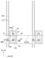
이하에서는 도 1 및 도 2를 참고하여 본 발명의 일 실시예에 따른 박막 트랜지스터 표시판에 대해 설명한다. 도 1은 본 발명의 일 실시예에 따른 일 화소의 평면도이고, 도 2는 도 1의 II-II선을 따라 자른 단면도이다.Hereinafter, a thin film transistor panel according to an embodiment of the present invention will be described with reference to FIGS. 1 and 2. FIG. FIG. 1 is a plan view of one pixel according to an embodiment of the present invention, and FIG. 2 is a cross-sectional view taken along line II-II of FIG.
유리 또는 플라스틱 등으로 만들어진 기판(110) 위에 데이터선(171) 및 광차단층(172)이 위치한다. A
데이터선(171)은 데이터 신호를 전달하며, 제1 방향으로 연장될 수 있다. 데이터선(171)은 단일막 또는 다중막으로 만들어질 수 있으며, 알루미늄(Al), 은(Ag), 구리(Cu), 크롬(Cr), 몰리브덴(Mo), 탄탈륨(Ta) 및 티타늄(Ti) 등의 금속 또는 이들의 합금 등의 도전성 물질로 만들어질 수 있다. The
광차단층(172)은 후술할 산화물 반도체층(154)에 빛이 도달하는 것을 막아 누설 전류 등 박막 트랜지스터의 채널 특성 저하를 방지한다. 이를 위해 본 발명의 일 실시예에 따른 광차단층(172)은 박막 트랜지스터(Q)와 중첩하도록 위치한다. The
광차단층(172)은 데이터선(171)과 동일 층에 위치할 수 있으며 동일 공정을 통해 형성될 수 있다. 이에 따라 광차단층(172)은 데이터선(171)과 동일한 재질일 수 있다. 그러나 이에 제한되지 않고 소정의 광을 투과시키지 않는 어떠한 재료도 가능함은 물론이며, 데이터선(171)과 상이한 유기 절연 물질, 무기 절연 물질 등 어떠한 물질로 이루어질 수 있다. The
광차단층(172)은 실시예에 따라 생략될 수 있다. 구체적으로 기판(110)을 통해, 산화물 반도체층(154)에 광이 입사되지 않는 경우에는 생략 가능하다. 예를 들어 박막 트랜지스터 표시판이 유기 발광 표시 장치 등에 사용되는 경우, 광차단층(172)은 생략될 수 있다. The
버퍼층(111)이 광차단층(172) 위에 위치하고, 박막 트랜지스터(Q)와 중첩한다. 도 1에 도시된 바와 같이 버퍼층(111)은 광차단층(172), 박막 트랜지스터(Q)와 중첩하고, 게이트선(121)이 버퍼층(111)을 가로지르도록 위치할 수 있다. The
버퍼층(111)은 두께가 상이한 제1 영역(111a) 및 제2 영역(111b)을 포함할 수 있다. 본 발명의 일 실시예에 따르면, 제1 영역(111a)은 후술할 산화물 반도체층(154), 소스 전극(173) 및 드레인 전극(175)과 중첩할 수 있으며, 제2 영역(111b)은 제1 영역(111a)을 제외한 나머지 영역을 나타낸다. The
이때 제1 영역(111a)의 두께는 제2 영역(111b)의 두께보다 두꺼울 수 있다. 이는 버퍼 물질층을 형성하고 식각하는 과정에서, 산화물 반도체층(154) 등과 중첩하는 제1 영역(111a)은 식각되지 않고 보호받는 반면 제2 영역(111b)의 일부는 식각되어 제거되기 때문이다. 이에 대하여, 뒤에서 구체적으로 설명한다.At this time, the thickness of the
제2 영역(111b)은 광차단층(172)의 가장자리 부분과 중첩하도록 위치할 수 있다. 따라서 제2 영역(111b)은 광차단층(172)의 상부면 가장자리, 측면 그리고 기판(110)의 상부면과 접촉하도록 위치한다. 이에 따라 위치하는 제2 영역(111b)의 단면은 계단 형상일 수 있다. 그러나 이에 제한되지 않고 제2 영역(111b)은 광차단층(172)의 가장자리 부분의 상부면 위에만 위치하는 실시예도 가능함은 물론이다. The
버퍼층(111)은 질화실리콘(SiNx), 산화실리콘(SiOx), 산화알루미늄(Al2O3), 산화하프늄(HfO3), 산화이트륨(Y2O3) 등의 절연성 산화물을 포함할 수 있다. 버퍼층(111)은 기판(110)으로부터 산화물 반도체층(154)에 불순물이 유입되는 것을 막아 산화물 반도체층(154)을 보호하고 반도체의 계면 특성을 향상시킬 수 있다.
버퍼층(111)과 기판(110) 사이에 위치하는 데이터선(171) 또는 광차단층(172)이 금속 재질인 경우, 버퍼층(111)은 이중막 구조일 수 있다. 구체적으로, 버퍼층(111) 중 광차단층(172)과 접하는 일 층은 제조 공정 상에서 발생하는 부식 등을 방지하기 위해 질화실리콘을 포함하고, 버퍼층(111) 중 산화물 반도체층(154)과 접하는 일 층은 산화실리콘 등을 포함할 수 있다. When the
한편 버퍼층(111)의 두께는 10 nm 이상 1000 nm 이하일 수 있으며 이에 한정되는 것은 아니다.On the other hand, the thickness of the
버퍼층(111) 위에 산화물 반도체층(154), 소스 전극(173) 및 드레인 전극(175)이 위치한다. The
산화물 반도체층(154)은 산화물 반도체 물질을 포함하는 단일막 또는 다중막일 수 있다. 산화물 반도체 물질은 금속 산화물 반도체로써, 아연(Zn), 인듐(In), 갈륨(Ga), 주석(Sn), 티타늄(Ti) 등의 금속의 산화물 또는 아연(Zn), 인듐(In), 갈륨(Ga), 주석(Sn), 티타늄(Ti) 등의 금속과 이들의 산화물의 조합으로 이루어질 수 있다. 예를 들어, 산화물 반도체 물질은 산화아연(ZnO), 아연-주석산화물(ZTO), 아연-인듐산화물(ZIO), 인듐산화물(InO), 티타늄산화물(TiO), 인듐-갈륨-아연산화물(IGZO), 인듐-아연-주석산화물(IZTO) 중 적어도 하나를 포함할 수 있다.The
소스 전극(173) 및 드레인 전극(175)은 산화물 반도체층(154)을 중심으로 양쪽에 각각 위치하며 산화물 반도체층(154)과 연결되어 있다. The
산화물 반도체층(154)의 두께는 약 600 Å 이하일 수 있으며, 이와 연결되는 소스 전극(173) 및 드레인 전극(175) 역시 동일한 두께를 가질 수 있다. The thickness of the
소스 전극(173) 및 드레인 전극(175)은 도전성을 가지며 산화물 반도체층(154)을 이루는 산화물 반도체 물질과 동일한 물질 및 환원된 반도체 물질을 포함할 수 있다. 소스 전극(173) 및 드레인 전극(175)의 표면에는 산화물 반도체 물질에 포함된 인듐(In) 등의 금속이 석출되어 있을 수 있다.The
산화물 반도체층(154) 위에 게이트 절연막(140)이 위치한다. 게이트 절연막(140)은 산화물 반도체층(154)의 계면 특성을 향상시키고 산화물 반도체층(154)에 불순물이 침투하는 것을 방지할 수 있다.A
게이트 절연막(140)은 산화물 반도체층(154)과 중첩하며, 소스 전극(173) 또는 드레인 전극(175)과는 실질적으로 중첩하지 않을 수 있다. The
게이트 절연막(140)의 두께는 약 1000Å 이상 약 5000Å 이하일 수 있으나, 이에 한정되는 것은 아니다. 게이트 절연막(140)의 전체 두께는 박막 트랜지스터의 특성에 따라 변화 가능하다.The thickness of the
게이트 절연막(140) 위에 게이트 전극(124)이 위치한다. 본 발명의 일 실시예에 따라 게이트 전극(124)과 게이트 절연막(140)의 가장자리는 실질적으로 중첩할 수 있으며, 서로 상하 정렬될 수 있다. A
게이트 전극(124)은 산화물 반도체층(154)과 중첩하며, 산화물 반도체층(154)은 게이트 전극(124)에 의해 덮여 있다. 게이트 전극(124)을 중심으로 산화물 반도체층(154)의 양쪽에는 소스 전극(173) 및 드레인 전극(175)이 위치하며, 소스 전극(173) 및 드레인 전극(175)은 게이트 전극(124)과 실질적으로 중첩하지 않을 수 있다. 따라서 게이트 전극(124)과 소스 전극(173) 사이의 기생 용량 또는 게이트 전극(124)과 드레인 전극(175) 사이의 기생 용량이 작아질 수 있다.The
게이트 전극(124)은 알루미늄(Al), 은(Ag), 구리(Cu), 몰리브덴(Mo), 크롬(Cr), 탄탈륨(Ta), 티타늄(Ti) 등의 금속 또는 이들의 합금 등을 포함할 수 있다. 게이트 전극(124)은 단일막 또는 다중막 구조를 가질 수 있다. 다중막의 예로는 티타늄(Ti), 탄탈륨(Ta), 몰리브덴(Mo), ITO 등의 하부막과 구리(Cu) 등의 상부막의 이중막, 몰리브덴(Mo)-알루미늄(Al)-몰리브덴(Mo)의 삼중막 등을 들 수 있다. 그러나 게이트 전극(124)은 이외에도 여러 가지 다양한 금속 또는 도전체로 만들어질 수 있다.The
게이트 전극(124), 소스 전극(173) 및 드레인 전극(175)은 산화물 반도체층(154)과 함께 박막 트랜지스터(Thin Film Transistor, TFT)(Q)를 이루며, 박막 트랜지스터의 채널(channel)은 산화물 반도체층(154)에 형성된다.The
게이트 전극(124), 소스 전극(173), 드레인 전극(175), 버퍼층(111) 및 기판(110) 위에 제1 보호막(180a)이 위치한다. 제1 보호막(180a)은 질화실리콘 또는 산화실리콘 등의 무기 절연 물질 또는 유기 절연 물질 등으로 이루어질 수 있다. The first
제1 보호막(180a) 위에 색필터(230)가 위치할 수 있다. 색필터(230)는 적색 색필터, 녹색 색필터 및 청색 색필터가 제1 방향 또는 제2 방향을 따라 반복될 수 있다. 적색 색필터, 녹색 색필터 및 청색 색필터 각각은 하나의 단위 화소를 형성하고, 하나의 단위 화소는 색필터를 투과하여 방출되는 광을 통해 소정의 컬러 영상을 표시한다. 실시예에 따라 색필터(230)는 생략될 수 있다. The
색필터(230) 위에 제2 보호막(180b)이 위치할 수 있다. 제2 보호막(180b)은 질화실리콘 또는 산화실리콘 등의 무기 절연 물질로 이루어지거나, 실시예에 따라 유기 절연 물질로 이루어질 수 있다. The second
제1 보호막(180a), 색필터(230) 및 제2 보호막(180b) 중 적어도 하나는 데이터선(171)의 일부와 중첩하는 제1 접촉 구멍(185a), 소스 전극(173)의 일부와 중첩하는 제2 접촉 구멍(185b), 드레인 전극(175)의 일부와 중첩하는 제3 접촉 구멍(185c)을 가질 수 있다.At least one of the first
제2 보호막(180b) 위에 화소 전극(191) 및 연결 전극(192)이 위치할 수 있다. The
연결 전극(192)은 제1 접촉 구멍(185a) 및 제2 접촉 구멍(185b)을 통해 데이터선(171)과 소스 전극(173)을 전기적으로 연결하고, 데이터선(171)으로부터 전달받은 데이터 신호를 소스 전극(173)으로 전달한다. The
화소 전극(191)은 제3 접촉 구멍(185c)을 통해 드레인 전극(175)과 물리적, 전기적으로 연결된다. 본 명세서는 화소 전극(191)이 제3 접촉 구멍(185c)을 통해 드레인 전극(175)과 직접 연결되는 실시예를 설명하였으나, 이에 제한되지 않고 화소 전극(191)은 별도의 연결 전극(미도시)을 통해 드레인 전극(175)과 물리적, 전기적으로 연결될 수 있음은 물론이다. The
이하에서는 도 3 및 도 4를 참고하여 변형 실시예에 따른 박막 트랜지스터 표시판에 대해 설명한다. 도 3은 도 1의 변형 실시예에 따른 평면도이고, 도 4는 도 3의 IV-IV선을 따라 자른 단면도이다. 이하에서는 전술한 구성요소와 다른 구성요소에 대해 설명하며, 동일한 구성요소에 대한 설명은 생략한다. Hereinafter, a thin film transistor panel according to a modified embodiment will be described with reference to FIGS. 3 and 4. FIG. FIG. 3 is a plan view according to a modified embodiment of FIG. 1, and FIG. 4 is a sectional view taken along the line IV-IV of FIG. Hereinafter, components other than those described above will be described, and description of the same components will be omitted.
본 발명의 변형 실시예에 따른 박막 트랜지스터 표시판에서, 산화물 반도체층(154) 위에 게이트 절연막(140) 및 게이트 전극(124)이 위치한다. In the thin film transistor display panel according to the modified embodiment of the present invention, the
이때 게이트 전극(124)의 제1 방향 가장자리는 게이트 절연막(140)의 제1 방향 가장자리보다 내측으로 위치할 수 있다. 다시 말해, 게이트 절연막(140)의 제1 방향 폭은 게이트 전극(124)의 제1 방향 폭보다 클 수 있다.At this time, the first directional edge of the
이처럼, 게이트 전극(124)이 게이트 절연막(140)보다 좁은 폭을 가짐으로써, 게이트 전극(124)과 소스 전극(173) 또는 게이트 전극(124)과 드레인 전극(175) 사이의 간격이 넓어질 수 있다. 이에 따라 게이트 전극(124)과 소스 전극(173) 또는 게이트 전극(124)과 드레인 전극(175) 사이의 기생 용량을 감소시킬 수 있으며, 기생 용량이 감소하는 경우, 박막 트랜지스터의 온-오프 특성이 향상될 수 있다. The gap between the
이하에서는 도 5 및 도 6을 참고하여 변형 실시예에 따른 박막 트랜지스터 표시판에 대해 설명한다. 도 5는 도 1의 변형 실시예에 따른 단면도이고, 도 6은 도 5의 VI-VI선을 따라 자른 단면도이다. 이하에서는 전술한 구성요소와 다른 구성요소에 대해 설명하며, 동일한 구성요소에 대한 설명은 생략한다.Hereinafter, a thin film transistor panel according to a modified embodiment will be described with reference to FIGS. 5 and 6. FIG. FIG. 5 is a cross-sectional view taken along line VI-VI of FIG. 5, and FIG. 6 is a cross-sectional view taken along line VI-VI of FIG. Hereinafter, components other than those described above will be described, and description of the same components will be omitted.
도 5에 도시된 바와 같이 제2 접촉 구멍(185b) 및 제3 접촉 구멍(185c)은 소스 전극(173) 및 드레인 전극(175)의 가장자리와 중첩할 수 있다. 이처럼, 접촉 구멍을 가장자리와 중첩하도록 형성함으로써, 소스 전극(173) 및 드레인 전극(175)의 제1 방향 폭, 즉 연결 전극(192) 또는 화소 전극(191)과 연결 가능한 영역이 작아지는 경우에도 이들의 접촉 마진을 확보할 수 있다. The
따라서 도 5 및 도 6과 같은 변형 실시예의 경우, 제조 공정 상에 발생 가능한 미스 얼라인에 의한 단선 등을 방지할 수 있으며 일 화소 영역의 마진 등을 최소화할 수 있는 이점이 있다. Therefore, in the modified embodiment shown in FIGS. 5 and 6, it is possible to prevent disconnection due to misalignment that may occur in the manufacturing process, and to minimize margins in one pixel region.
이하에서는 도 7 내지 도 15를 참고하여 본 발명의 일 실시예에 따른 박막 트랜지스터 표시판의 제조 방법에 대해 설명한다. 도 7, 도 8, 도 9, 도 10, 도 11, 도 12, 도 13, 도 14 및 도 15는 제조 공정에 따른 박막 트랜지스터 표시판의 단면도이다. Hereinafter, a method of manufacturing a thin film transistor panel according to an embodiment of the present invention will be described with reference to FIGS. 7 to 15. FIG. 7, 8, 9, 10, 11, 12, 13, 14, and 15 are cross-sectional views of a thin film transistor panel according to a manufacturing process.
우선, 도 7을 참고하면, 기판(110) 위에 데이터 도전층을 형성하고 이를 패터닝하여 데이터선(171) 및 광차단층(172)을 형성하고, 기판(110), 데이터선(171) 및 광차단층(172) 위에 버퍼 물질층(BL)을 형성한다. 이때 광차단층(172)은 실시예에 따라 생략될 수 있다. 7, a data conductive layer is formed on a
또한 본 명세서는 데이터선(171) 및 광차단층(172)이 동일 공정을 통해 형성되는 실시예를 설명하였으나, 이에 제한되지 않고 유기 절연 물질, 무기 절연 물질 등으로 이루어진 광차단층(172)을 형성한 후 금속 등을 적층 및 패터닝하여 데이터선(171)을 형성하는 실시예도 가능하다. 광차단층(172) 및 데이터선(171)의 형성 순서가 바뀔 수 있음은 물론이다.Although the present invention has been described with reference to the embodiments in which the
버퍼 물질층(BL)은 화학 기상 증착법(chemical vapor deposition, CVD) 등의 방법으로 형성될 수 있으며, 질화실리콘(SiNx), 산화실리콘(SiOx), 산화알루미늄(Al2O3), 산화하프늄(HfO3), 산화이트륨(Y2O3) 등의 절연성 산화물을 포함할 수 있다. 또한 버퍼 물질층(BL)의 두께는 10 nm 이상 1000 nm 이하일 수 있다. 그러나 버퍼 물질층(BL)은 이러한 제조 방법, 재질 및 두께에 한정되지 않으며 산화물 반도체층을 보호하기 위한 어떠한 제조 방법, 재질 및 두께도 가능하다. The buffer material layer (BL) is a CVD (chemical vapor deposition, CVD) can be formed by methods such as, silicon nitride (SiNx), silicon oxide (SiOx), aluminum oxide (Al 2 O 3), hafnium oxide ( HfO 3 ), yttrium oxide (Y 2 O 3 ), and the like. The thickness of the buffer material layer (BL) may be 10 nm or more and 1000 nm or less. However, the buffer material layer (BL) is not limited to such a manufacturing method, material and thickness, and any manufacturing method, material and thickness for protecting the oxide semiconductor layer are possible.
다음 도 8을 참고하면, 버퍼 물질층(BL) 위에 산화물 반도체 물질층을 형성하고 이를 패터닝하여 제1 산화물 반도체 패턴(154P1)을 형성한다. 제1 산화물 반도체 패턴(154P1)은 광차단층(172)과 중첩하도록 패터닝될 수 있다. Referring to FIG. 8, a layer of an oxide semiconductor material is formed on the buffer material layer BL and patterned to form a first oxide semiconductor pattern 154P1. The first oxide semiconductor pattern 154P1 may be patterned to overlap with the
제1 산화물 반도체 패턴(154P1)은 산화물 반도체 물질로 이루어질 수 있다. 산화물 반도체 물질은 금속 산화물 반도체로써, 아연(Zn), 인듐(In), 갈륨(Ga), 주석(Sn), 티타늄(Ti) 등의 금속의 산화물 또는 아연(Zn), 인듐(In), 갈륨(Ga), 주석(Sn), 티타늄(Ti) 등의 금속과 이들의 산화물의 조합으로 이루어질 수 있다. 예를 들어, 산화물 반도체 물질은 산화아연(ZnO), 아연-주석산화물(ZTO), 아연-인듐산화물(ZIO), 인듐산화물(InO), 티타늄산화물(TiO), 인듐-갈륨-아연산화물(IGZO), 인듐-아연-주석산화물(IZTO) 중 적어도 하나를 포함할 수 있다.The first oxide semiconductor pattern 154P1 may be made of an oxide semiconductor material. The oxide semiconductor material is a metal oxide semiconductor and may be an oxide of a metal such as zinc (Zn), indium (In), gallium (Ga), tin (Sn), titanium (Ti) (Ga), tin (Sn), titanium (Ti), and oxides thereof. For example, the oxide semiconductor material may be selected from the group consisting of zinc oxide (ZnO), zinc-tin oxide (ZTO), zinc-indium oxide (ZIO), indium oxide (InO), titanium oxide (TiO), indium- ), And indium-zinc-tin oxide (IZTO).
다음 도 9를 참고하면, 버퍼 물질층(BL) 및 제1 산화물 반도체 패턴(154P1) 위에 절연 재질인 게이트 절연막 물질층(GI) 및 도전 재질인 게이트 도전층(GM)을 형성한다. 그리고 나서 게이트 도전층(GM) 위에 게이트 도전층(GM) 및 게이트 절연막 물질층(GI)을 패터닝하기 위한 마스크 패턴(M)을 형성한다.Next, referring to FIG. 9, a gate insulating film material layer GI, which is an insulating material, and a gate conductive layer GM, which is a conductive material, are formed over the buffer material layer BL and the first oxide semiconductor pattern 154P1. Then, a mask pattern M for patterning the gate conductive layer GM and the gate insulating film material layer GI is formed on the gate conductive layer GM.
다음 도 10에 도시된 바와 같이, 게이트 도전층(GM)을 습식 식각하여 게이트 전극(124)을 형성하고, 게이트 절연막 물질층(GI)을 식각하여 게이트 절연막 패턴(140P)을 형성한다. 게이트 전극(124) 및 게이트 절연막 패턴(140P)은 제1 산화물 반도체 패턴(154P1)의 가운데 부분을 가로지르며 통과하도록 형성되며, 게이트 전극(124)과 제1 산화물 반도체 패턴(154P1)의 중첩 부분의 양쪽에 위치하는 제1 산화물 반도체 패턴(154P1)의 두 영역은 게이트 전극(124)과 중첩하지 않는다. 10, a
이때 게이트 전극(124)의 제1 방향 가장자리는 가상의 선 L1을 형성하고, 게이트 절연막 패턴(140P)의 제1 방향 가장자리는 가상의 선 L2를 형성하며, 제1 산화물 반도체 패턴(154P1)의 제1 방향 가장자리는 가상의 선 L3를 형성할 수 있다. At this time, the first direction edge of the
다음 도 11에 도시된 바와 같이, 게이트 전극(124) 위에 위치하는 마스크 패턴(M)을 제거하고 추가 식각을 실시할 수 있다. 11, the mask pattern M located on the
추가 식각을 통해, 도 12에 도시된 바와 같이, L1과 L2 사이에 위치하는 게이트 절연막 패턴(140P)의 일부가 제거되어 게이트 절연막(140)이 형성되고, L2 및 L3 사이에 위치하는 제1 산화물 반도체 패턴(154P1)의 일부가 제거되어 제2 산화물 반도체 패턴(154P2)이 형성되고, L3를 기준으로 외측에 위치하는 버퍼 물질층(BL)이 제거되어 버퍼층(111)을 형성한다. 버퍼층(111)은 제1 산화물 반도체 패턴(154P1)과 중첩하는 영역에 위치한다. 12, a part of the gate insulating
버퍼 물질층(BL) 중 제2 산화물 반도체 패턴(154P2)과 중첩하는 영역에 위치하는 부분은 전혀 제거되지 않아 소정의 두께를 가지는 제1 영역(111a)을 이루고, L2 및 L3 사이에 위치하는 부분은 제1 산화물 반도체 패턴(154P1)이 제거되는 공정에서 식각 선택비에 의해 일부 제거됨으로써, 제1 영역(111a) 보다 얇은 두께를 가지는 제2 영역(111b)을 이루게 된다. The portion of the buffer material layer BL which overlaps with the second oxide semiconductor pattern 154P2 is not removed at all and forms a
앞서 설명한 바와 같이, 버퍼 물질층(BL) 중 제1 산화물 반도체 패턴(154P1)과 중첩하지 않는 부분은 모두 제거된다. 즉, 데이터선(171)과 중첩하는 버퍼 물질층(BL)이 제거된다. 따라서 본 발명의 실시예에 따른 버퍼층(111)은 데이터선(171)과 중첩하지 않을 수 있다. As described above, all portions of the buffer material layer BL that do not overlap with the first oxide semiconductor pattern 154P1 are removed. That is, the buffer material layer BL overlapping with the
다음, 도 13을 참고하면 제2 산화물 반도체 패턴(154P2)에서 게이트 전극(124) 및 게이트 절연막(140)과 중첩하지 않는 두 영역을 환원 처리하여, 도전성을 가지는 소스 전극(173) 및 드레인 전극(175)을 형성한다. 이때 게이트 전극(124) 및 게이트 절연막(140)과 중첩하여 환원되지 않은 제2 산화물 반도체 패턴(154P2)은 채널을 이루는 산화물 반도체층(154)이 된다. 13, two regions of the second oxide semiconductor pattern 154P2 which do not overlap the
구체적으로 제2 산화물 반도체 패턴(154P2)의 환원 처리 방법은 환원 분위기에서의 열처리 방법일 수 있고, 수소(H2), 헬륨(He), 포스핀(PH3), 암모니아(NH3), 실란(SiH4), 메탄(CH4), 아세틸렌(C2H2), 디보란(B2H6), 이산화탄소(CO2), 저메인(GeH4), 셀렌화수소(H2Se), 황화수소(H2S), 아르곤(Ar), 질소(N2), 산화 질소(N2O), 플루오르포름(CHF3) 등 기체 플라즈마를 이용한 플라즈마 처리 방법일 수도 있다. 환원 처리되며 제2 산화물 반도체 패턴(154P2)을 구성하는 반도체 물질의 적어도 일부는 환원되어 금속 결합만이 남을 수 있다. 따라서 환원 처리된 제2 산화물 반도체 패턴(154P2)은 도전성을 가지게 된다.Specifically, the reduction method of the second oxide semiconductor pattern (154P2) may be a heat treatment in a reducing atmosphere, the hydrogen (H 2), helium (He), phosphine (PH 3), ammonia (NH 3), silane (SiH 4), methane (CH 4), acetylene (C 2 H 2), diborane (B 2 H 6), carbon dioxide (CO 2), germane (GeH 4), hydrogen selenide (H 2 Se), hydrogen sulfide ( Plasma treatment using a gas plasma such as argon (H 2 S), argon (Ar), nitrogen (N 2 ), nitrogen oxide (N 2 O) or fluoroform (CHF 3 ). At least a part of the semiconductor material constituting the second oxide semiconductor pattern 154P2 is reduced and only the metal bond may be left. Therefore, the second oxide semiconductor pattern 154P2 subjected to the reduction treatment has conductivity.
이렇게 형성된 게이트 전극(124), 소스 전극(173), 드레인 전극(175) 및 산화물 반도체층(154)은 박막 트랜지스터(Q)를 이룬다.The
도 13을 참고하면, 게이트 전극(124), 소스 전극(173), 드레인 전극(175) 등을 덮도록 제1 보호 물질층(PL1)을 형성하고, 그 위에 색필터(230)를 도포하고, 색필터(230)를 패터닝하여 제1 접촉 구멍(185a), 제2 접촉 구멍(185b), 제3 접촉 구멍(185c)이 형성될 부분에 위치하는 색필터(230)를 제거한다. 13, a first passivation layer PL1 is formed to cover the
도 14에 도시된 바와 같이 색필터(230) 위에 위치하는 제2 보호 물질층(PL2)을 형성한다. 제2 보호 물질층(PL2)은 제1 보호 물질층(PL1)과 동일한 재질이거나 상이한 재질일 수 있다. A second protective material layer PL2 is formed on the
다음 도 15에 도시된 바와 같이 제2 보호 물질층(PL2) 및 제1 보호 물질층(PL1)을 패터닝하여 데이터선(171)의 일부와 중첩하는 제1 접촉 구멍(185a), 소스 전극(173)의 일부와 중첩하는 제2 접촉 구멍(185b), 및 드레인 전극(175)의 일부와 중첩하는 제3 접촉 구멍(185c)을 가지는 제2 보호막(180b) 및 제1 보호막(180a)을 형성한다. 이때 제2 보호 물질층(PL2) 및 제1 보호 물질층(PL1)은 건식 식각을 통해 패터닝될 수 있다.The
다음, 제2 보호막(180b) 위에 도전층을 도포하고 패터닝하여, 제1 접촉 구멍(185a) 및 제2 접촉 구멍(185b)을 통해 데이터선(171)과 소스 전극(173)을 연결하는 연결 전극(192)을 형성하고, 제3 접촉 구멍(185c)을 통해 드레인 전극(175)과 연결되는 화소 전극(191)을 형성하여, 도 2에 도시된 박막 트랜지스터 표시판을 형성한다. Next, a conductive layer is applied and patterned on the second
정리하면, 도 7 내지 도 15에 따른 박막 트랜지스터 표시판의 제조 방법은 1차 식각을 통해 게이트 전극 및 게이트 절연 패턴을 형성하고, 이후 마스크 패턴을 제거한 후, 게이트 전극을 마스크로 하여 2차 식각을 진행한다. 2차 식각에서 게이트 절연막을 형성하고, 소스 전극 및 드레인 전극을 형성하기 위한 제2 산화물 반도체 패턴을 형성하고, 데이터선과 중첩하지 않도록 일부 영역이 제거된 버퍼층을 형성한다. In summary, in the method of manufacturing the thin film transistor panel according to FIGS. 7 to 15, the gate electrode and the gate insulating pattern are formed through the first etching, the mask pattern is removed, and the second etching is performed using the gate electrode as the mask do. A gate insulating film is formed in the second etching, a second oxide semiconductor pattern for forming the source electrode and the drain electrode is formed, and a buffer layer in which a part of the region is not overlapped with the data line is formed.
전술한 박막 트랜지스터 표시판의 제조 방법에서, 접촉 구멍을 형성하기 위해서는 제1 보호 물질층(PL1) 및 제2 보호 물질층(PL2)을 제거한다. 구체적으로, 제1 접촉 구멍(185a), 제2 접촉 구멍(185b) 및 제3 접촉 구멍(185c)을 형성할 때, 제1 보호 물질층(PL1) 및 제2 보호 물질층(PL2)을 식각한다. 이처럼, 복수의 접촉 구멍을 동시에 형성함에 있어 동일한 물질층을 동시에 식각하기 때문에, 각 접촉 구멍은 동일한 식각비로 형성될 수 있다. In the above-described manufacturing method of the thin film transistor panel, the first protective material layer PL1 and the second protective material layer PL2 are removed to form contact holes. Specifically, when the
특히 데이터선(171)의 일부와 중첩하는 제1 접촉 구멍(185a)을 형성할 때, 데이터선(171)과 중첩하는 부분에 위치하는 버퍼 물질층이 기제거된 상태이기 때문에, 데이터선(171)의 일부와 중첩하는 제1 접촉 구멍(185a)을 형성할 때에도, 제2 접촉 구멍(185b) 및 제3 접촉 구멍(185c)을 형성하는 식각 공정과 동일한 물질을 제거하도록 진행될 수 있다. Particularly, when forming the
제1 접촉 구멍(185a)이 버퍼 물질층과도 중첩하는 경우, 제2 접촉 구멍(185b) 및 제3 접촉 구멍(185c)을 형성한 후에도, 제1 접촉 구멍(185a)과 중첩하는 버퍼 물질층을 추가로 식각하여야 하기 때문에, 추가 식각 공정을 통해 버퍼 물질층을 식각하는 동안, 제2 접촉 구멍(185b) 및 제3 접촉 구멍(185c)과 중첩하는 소스 전극(173) 및 드레인 전극(175)의 표면이 손상될 수 있다.When the
이에 대하여 구체적으로 설명한다.This will be described in detail.
본 발명의 실시예와 달리 데이터선과 중첩하는 버퍼 물질층이 제거되지 않은 경우, 제1 접촉 구멍을 형성하기 위해서는 버퍼 물질층(BL), 제1 보호 물질층(PL1), 제2 보호 물질층(PL2)을 식각하고, 제2 접촉 구멍 및 제3 접촉 구멍을 형성하기 위해서는 제1 보호 물질층(PL1) 및 제2 보호 물질층(PL2)을 식각하여야 한다. In order to form the first contact hole, the buffer material layer BL, the first protective material layer PL1, the second protective material layer (not shown) PL2) are etched. In order to form the second contact hole and the third contact hole, the first protective material layer PL1 and the second protective material layer PL2 should be etched.
제1 보호 물질층(PL1) 및 제2 보호 물질층(PL2)이 식각된 이후, 제1 접촉 구멍(185a)이 위치할 영역에는 버퍼 물질층(BL)이 위치하고, 제2 및 제3 접촉 구멍(185b, 185c)이 위치할 영역에는 산화물 반도체층(또는 환원된 산화물 반도체층, 즉 소스 전극 및 드레인 전극)이 위치한다.After the first protective material layer PL1 and the second protective material layer PL2 are etched, a buffer material layer BL is located in a region where the
따라서 제1 접촉 구멍(185a)을 형성하기 위해 버퍼 물질층(BL)을 식각하는 경우, 산화물 반도체층의 식각을 수반하게 된다. 이때 산화물 반도체층의 손상을 최소화하기 위해서는 적어도 40:1의 선택 식각비가 요구되며, 이러한 고선택 식각비를 유지하기 어렵다. Therefore, when the buffer material layer BL is etched to form the
제2 보호 물질층(PL2)이 유기 물질인 경우도 유사하다. 더욱이, 제2 보호 물질층(PL2)이 유기막인 경우, 버퍼 물질층(BL)을 식각하는 동안 산화물 반도체층뿐만 아니라 유기 물질인 제2 보호 물질층도 손상될 수 있다.The case where the second protective material layer PL2 is an organic material is also similar. Furthermore, when the second protective material layer PL2 is an organic film, the second protective material layer which is an organic material as well as the oxide semiconductor layer can be damaged during etching the buffer material layer BL.
그러나, 본 실시예에 따르면 제1 접촉 구멍(185a)이 중첩하는 데이터선(171)과 중첩하는 부분에서 버퍼 물질층이 기제거되기 때문에, 제1 접촉 구멍(185a), 제2 접촉 구멍(185b) 및 제3 접촉 구멍(185c)이 같은 식각 조건으로 형성될 수 있어, 공정 조건이 단순하고, 식각 공정 중 발생할 수 있는 소스 전극(173) 및 드레인 전극(175)의 손상을 방지하여 신뢰성이 향상된 박막 트랜지스터를 제공할 수 있다. However, according to the present embodiment, since the buffer material layer is removed at the portion overlapping the
이처럼, 본 발명의 실시예에 따른 제조 방법과 같이 제1 접촉 구멍을 형성하는 위치에서 버퍼층이 기제거되는 경우, 접촉 구멍을 형성하는 공정에서 고 선택비를 가지는 식각 공정이 불필요하고, 이에 따라 공정이 단순화되며 박막 트랜지스터의 손상을 방지하여 신뢰성을 유지할 수 있다. As described above, when the buffer layer is removed at the position where the first contact hole is formed as in the manufacturing method according to the embodiment of the present invention, an etching process having a high selectivity ratio is not required in the process of forming the contact hole, The reliability of the thin film transistor can be maintained.
본 명세서는 박막 트랜지스터와 중첩하는 영역을 제외한 영역의 버퍼 물질층이 모두 제거되는 실시예에 대해 설명하였으나, 이에 제한되지 않고 제2 영역과 같이 얇은 두께의 버퍼 물질층이 기판(110) 전면에 위치하는 실시예도 가능할 것이다. 이에 따르면 전술한 바와 같이 40:1의 식각 선택비까지는 아니더라도 1:5 내지 1:20 수준의 낮은 식각 선택비만으로도 박막 트랜지스터의 손상 없이 접촉 구멍을 형성할 수 있다. Although the present invention has been described with respect to the embodiment where the buffer material layer in the region excluding the region overlapping with the thin film transistor is completely removed, a thin buffer material layer such as the second region is formed on the front surface of the
이하에서는 도 16 및 도 17을 참고하여 변형 실시예에 따른 박막 트랜지스터 표시판의 제조 방법에 대해 설명한다. 도 16 및 도 17은 변형 제조 공정에 따른 박막 트랜지스터 표시판의 단면도이다. 이하에서는 전술한 실시예와 상이한 공정 및 구성요소에 대해 설명하며, 동일한 공정 및 구성요소에 대한 설명은 생략한다. Hereinafter, a method of manufacturing the thin film transistor panel according to the modified embodiment will be described with reference to FIGS. 16 and 17. FIG. 16 and 17 are sectional views of a thin film transistor panel according to a modified manufacturing process. Hereinafter, processes and components different from those of the above-described embodiments will be described, and description of the same processes and components will be omitted.
전술한 박막 트랜지스터 표시판의 제조 방법에서, 도 7 내지 도 10의 제조 공정까지 동일하게 실시한다. In the above-described manufacturing method of the thin film transistor panel, the manufacturing steps of FIGS. 7 to 10 are carried out in the same manner.
다음, 도 16에 도시된 바와 같이 게이트 전극(124)의 제1 방향 가장자리가 형성하는 L1과 정렬되도록 일부 애싱된 마스크 패턴(M')을 형성한다. 애싱하는 방법에는 제한이 없으며 산소 플라즈마 등을 이용할 수 있다. Next, a part of the ashed mask pattern M 'is formed so as to be aligned with L1 formed by the first directional edge of the
추가 식각을 통해, 도 17에 도시된 바와 같이, L1과 L2 사이에 위치하는 게이트 절연막 패턴(140P)이 제거되어 게이트 절연막(140)이 형성된다. 이때 게이트 절연막(140)의 제1 방향 가장자리는 게이트 전극(124)의 제1 방향 가장자리와 일치하도록 형성될 수 있다. 즉, 게이트 전극(124)과 게이트 절연막(140)의 제1 방향 폭은 실질적으로 동일할 수 있으며, 게이트 전극(124)과 게이트 절연막(140)은 실질적으로 동일한 평면 형상을 가질 수 있다. Through the additional etching, as shown in Fig. 17, the gate insulating
또한 도 17과 같이 L2 및 L3 사이에 위치하는 제1 산화물 반도체 패턴(154P1)이 제거되어 제2 산화물 반도체 패턴(154P2)이 형성되며, L3의 외측 영역으로 위치하는 버퍼 물질층(BL)이 제거되어 버퍼층(111)이 형성된다. 이때 버퍼층(111)은 제1 산화물 반도체 패턴(154P1)과 중첩하는 영역에만 위치한다. 17, the first oxide semiconductor pattern 154P1 located between L2 and L3 is removed to form the second oxide semiconductor pattern 154P2, and the buffer material layer BL located in the outer region of L3 is removed And a
버퍼 물질층(BL) 중 제2 산화물 반도체 패턴(154P2)과 중첩하는 영역에 위치하는 부분은 전혀 제거되지 않아 소정의 두께를 가지는 제1 영역(111a)을 형성하고, L2 및 L3 사이에 위치하는 버퍼 물질층(BL)은 제1 산화물 반도체 패턴(154P1)이 제거되는 공정에서 식각 선택비에 의해 일부 제거됨으로써 제1 영역(111a) 보다 얇은 두께를 가지는 제2 영역(111b)을 이루게 된다. A portion of the buffer material layer BL that overlaps the second oxide semiconductor pattern 154P2 is not removed at all and a
이후 마스크 패턴(M')을 제거하고, 도 13 내지 도 15의 제조 공정을 동일하게 반복한다. Thereafter, the mask pattern M 'is removed, and the manufacturing process of Figs. 13 to 15 is repeated in the same manner.
도 16 및 도 17에 따른 박막 트랜지스터 표시판의 제조 방법은, 1차 식각을 통해 게이트 전극 및 게이트 절연 패턴을 형성하고, 이후 마스크 패턴을 일부 애싱한 후, 애싱된 마스크 패턴을 사용하여 게이트 전극과 정렬되는 게이트 절연막을 형성한다. 또한 게이트 절연 패턴을 이용하여 제2 산화물 반도체 패턴을 형성하고, 제1 산화물 반도체 패턴 등을 이용하여 버퍼층을 형성할 수 있다. 16 and 17, a gate electrode and a gate insulating pattern are formed through a primary etching, and after a portion of the mask pattern is ashed, an ashing mask pattern is used to align the gate electrode and the gate electrode A gate insulating film is formed. Further, a second oxide semiconductor pattern can be formed using a gate insulating pattern, and a buffer layer can be formed using a first oxide semiconductor pattern or the like.
이하에서는 도 18 및 도 19를 참고하여 변형 실시예에 따른 박막 트랜지스터 표시판의 제조 방법에 대해 설명한다. 도 18 및 도 19는 변형 제조 공정에 따른 박막 트랜지스터 표시판의 단면도이다. 이하에서는 전술한 실시예와 상이한 공정 및 구성요소에 대해 설명하며, 동일한 공정 및 구성요소에 대한 설명은 생략한다.Hereinafter, a method of manufacturing the thin film transistor panel according to the modified embodiment will be described with reference to FIGS. 18 and 19. FIG. 18 and 19 are sectional views of a thin film transistor panel according to a modified manufacturing process. Hereinafter, processes and components different from those of the above-described embodiments will be described, and description of the same processes and components will be omitted.
전술한 박막 트랜지스터 표시판의 제조 방법에서, 도 7 내지 도 10의 제조 공정까지 동일하게 실시한다. In the above-described manufacturing method of the thin film transistor panel, the manufacturing steps of FIGS. 7 to 10 are carried out in the same manner.
다음, 도 18에 도시된 바와 같이 마스크 패턴(M'')의 제1 방향 가장자리가 게이트 전극(124)의 제1 방향 가장자리가 형성하는 L1과 게이트 절연막 패턴(140P)의 제1 방향 가장자리가 형성하는 L2 사이에 위치하도록, 마스크 패턴(M)의 일부를 애싱한다. 애싱하는 방법에는 제한이 없으며 산소 플라즈마 등을 이용할 수 있다.18, the first directional edge of the mask pattern M " is formed by L1 formed by the first directional edge of the
그리고 나서, 도 19에 도시된 바와 같이, 애싱된 마스크 패턴(M'')으로 추가 식각하면, 마스크 패턴(M'')의 가장자리와 L2 사이에 위치하는 게이트 절연막 패턴(140P)이 제거되어 애싱된 마스크 패턴(M'')의 가장자리에 정렬된 게이트 절연막(140)이 형성되고, L2 및 L3 사이에 위치하는 제1 산화물 반도체 패턴(154P1)이 제거되어 제2 산화물 반도체 패턴(154P2)이 형성되며, L3의 외측 영역으로 위치하는 버퍼 물질층(BL)이 모두 제거되어 광차단층(172)과 중첩하는 버퍼층(111)이 형성된다. 버퍼층(111)은 제1 산화물 반도체 패턴(154P1)과 중첩하는 영역에만 위치하고, 특히 데이터선(171)과 중첩하는 버퍼 물질층(BL)은 제거된다. 따라서 본 발명의 실시예에 따른 버퍼층(111)은 데이터선(171)과 중첩하지 않을 수 있다.19, the gate insulating
버퍼 물질층(BL) 중 제2 산화물 반도체 패턴(154P2)과 중첩하는 영역에 위치하는 부분은 전혀 제거되지 않아 소정의 두께를 가지는 제1 영역(111a)을 형성하고, L2 및 L3 사이에 위치하는 버퍼 물질층(BL)은 제1 산화물 반도체 패턴(154P1)이 제거되는 공정에서 식각 선택비에 의해 일부 제거됨으로써 제1 영역(111a) 보다 얇은 두께를 가지는 제2 영역(111b)을 이루게 된다. A portion of the buffer material layer BL that overlaps the second oxide semiconductor pattern 154P2 is not removed at all and a
이때 게이트 절연막(140)의 제1 방향 가장자리는 게이트 전극(124)의 제1 방향 가장자리의 외측에 위치하도록 형성될 수 있다. 다시 말해, 게이트 전극(124)의 제1 방향 폭은 게이트 절연막(140)의 제1 방향 폭 보다 작게 형성될 수 있다.At this time, the first direction edge of the
이후 마스크 패턴(M'')을 제거하고, 도 13 내지 도 15의 제조 공정을 동일하게 반복한다. Thereafter, the mask pattern M " is removed, and the manufacturing process of Figs. 13 to 15 is repeated in the same manner.
도 18 및 도 19의 변형 실시예에 따른 제조 방법은, 마스크 패턴을 이용한 1차 식각을 통해 게이트 전극 및 게이트 절연 패턴을 형성하고, 일부 애싱된 마스크를 이용한 2차 식각을 통해 게이트 전극보다 넓은 제1 방향 폭을 가지는 게이트 절연막을 형성하는 단계를 포함한다. 또한 게이트 절연 패턴을 이용하여 제2 산화물 반도체 패턴을 형성하고, 제1 산화물 반도체 패턴을 이용하여 버퍼층을 형성하는 단계를 포함할 수 있다. 18 and 19, a gate electrode and a gate insulating pattern are formed through a first etching process using a mask pattern, and a second etching process using a partially ashed mask is performed to form a gate electrode And forming a gate insulating film having a one-directional width. Forming a second oxide semiconductor pattern using a gate insulating pattern, and forming a buffer layer using the first oxide semiconductor pattern.
이때 마스크 패턴의 애싱양은 도 16 및 도 17에서 설명한 마스크 패턴의 애싱양 보다 적을 수 있다. 도 18 및 도 19에서 설명한 애싱된 마스크 패턴(M'')의 제1 방향 폭은 도 16 및 도 17의 애싱된 마스크 패턴(M')의 제1 방향 폭보다 클 수 있다. At this time, the ashing amount of the mask pattern may be smaller than the ashing amount of the mask pattern described with reference to FIG. 16 and FIG. The first directional width of the ashed mask pattern M '' described in FIGS. 18 and 19 may be greater than the first directional width of the ashed mask pattern M 'of FIGS.
앞에서, 본 발명의 특정한 실시예가 설명되고 도시되었지만 본 발명은 기재된 실시예에 한정되는 것이 아니고, 본 발명의 사상 및 범위를 벗어나지 않고 다양하게 수정 및 변형할 수 있음은 이 기술의 분야에서 통상의 지식을 가진 자에게 자명한 일이다. 따라서, 그러한 수정예 또는 변형예들은 본 발명의 기술적 사상이나 관점으로부터 개별적으로 이해되어서는 안되며, 변형된 실시예들은 본 발명의 특허청구범위에 속한다 하여야 할 것이다.While the present invention has been particularly shown and described with reference to exemplary embodiments thereof, it is to be understood that the invention is not limited to the disclosed embodiments, but, on the contrary, It is obvious to those who have. Accordingly, it should be understood that such modifications or alterations should not be understood individually from the technical spirit and viewpoint of the present invention, and that modified embodiments fall within the scope of the claims of the present invention.
110: 기판
111: 버퍼층
124: 게이트 전극
140: 게이트 절연막
154: 산화물 반도체층
171: 데이터선
172: 광차단층
173: 소스 전극
175: 드레인 전극
180a, 180b: 보호막
185a, 185b, 185c: 접촉 구멍110: substrate
111: buffer layer
124: gate electrode
140: gate insulating film
154: oxide semiconductor layer
171: Data line
172:
173: source electrode
175: drain electrode
180a, 180b:
185a, 185b, 185c:
Claims (20)
상기 기판 위에 위치하는 데이터선,
상기 기판 위에 위치하며 상기 데이터선과 중첩하지 않는 버퍼층,
상기 버퍼층 위에 위치하고, 산화물 반도체층을 포함하는 박막 트랜지스터, 그리고
상기 박막 트랜지스터와 연결된 화소 전극을 포함하는 박막 트랜지스터 표시판. Board,
A data line disposed on the substrate,
A buffer layer located on the substrate and not overlapping the data line,
A thin film transistor located on the buffer layer and including an oxide semiconductor layer, and
And a pixel electrode connected to the thin film transistor.
상기 데이터선과 동일한 층에 위치하며 상기 박막 트랜지스터와 중첩하는 광차단층을 더 포함하고,
상기 버퍼층은 상기 광차단층과 중첩하는 박막 트랜지스터 표시판. The method of claim 1,
Further comprising a light blocking layer located on the same layer as the data line and overlapping the thin film transistor,
And the buffer layer overlaps with the light blocking layer.
상기 버퍼층은 두께가 상이한 제1 영역 및 제2 영역을 포함하고,
상기 제2 영역은 상기 광차단층의 가장자리와 중첩하는 박막 트랜지스터 표시판. 3. The method of claim 2,
Wherein the buffer layer includes a first region and a second region having different thicknesses,
And the second region overlaps the edge of the light blocking layer.
상기 박막 트랜지스터는,
상기 산화물 반도체층과 동일한 층에 위치하고, 상기 산화물 반도체층을 중심으로 양쪽에 연결된 소스 전극 및 드레인 전극, 그리고
상기 산화물 반도체층과 중첩하는 게이트 전극을 더 포함하는 박막 트랜지스터 표시판. 4. The method of claim 3,
The thin-
A source electrode and a drain electrode located on the same layer as the oxide semiconductor layer and connected to both sides of the oxide semiconductor layer,
And a gate electrode overlapping the oxide semiconductor layer.
상기 소스 전극 및 상기 드레인 전극은 상기 산화물 반도체층을 이루는 물질이 환원된 물질을 포함하는 박막 트랜지스터 표시판. 5. The method of claim 4,
Wherein the source electrode and the drain electrode include a material in which the material of the oxide semiconductor layer is reduced.
상기 제1 영역은 상기 산화물 반도체층, 상기 소스 전극 및 상기 드레인 전극과 중첩하는 박막 트랜지스터 표시판. 5. The method of claim 4,
Wherein the first region overlaps the oxide semiconductor layer, the source electrode, and the drain electrode.
상기 산화물 반도체층 및 상기 게이트 전극 사이에 위치하는 게이트 절연막을 더 포함하고, 그리고
상기 데이터선은 제1 방향으로 연장되며,
상기 게이트 절연막의 제1 방향 폭은 상기 게이트 전극의 제1 방향 폭보다 큰 박막 트랜지스터 표시판. 5. The method of claim 4,
And a gate insulating film disposed between the oxide semiconductor layer and the gate electrode,
The data line extends in a first direction,
Wherein the first directional width of the gate insulating film is larger than the first directional width of the gate electrode.
상기 게이트 전극 위에 위치하는 제1 보호막을 더 포함하고,
상기 제1 보호막은
상기 데이터선과 중첩하는 제1 접촉 구멍,
상기 소스 전극과 중첩하는 제2 접촉 구멍, 그리고
상기 드레인 전극과 중첩하는 제3 접촉 구멍을 포함하는 박막 트랜지스터 표시판. 5. The method of claim 4,
Further comprising a first protective film located on the gate electrode,
The first protective film
A first contact hole overlapping the data line,
A second contact hole overlapping the source electrode, and
And a third contact hole overlapping the drain electrode.
상기 제2 접촉 구멍 및 제3 접촉 구멍은 상기 소스 전극 및 상기 드레인 전극의 가장자리와 중첩하는 박막 트랜지스터 표시판. 9. The method of claim 8,
And the second contact hole and the third contact hole overlap the edges of the source electrode and the drain electrode.
상기 제1 접촉 구멍 및 상기 제2 접촉 구멍을 통해 상기 데이터선과 상기 소스 전극을 연결하는 연결 전극을 포함하는 박막 트랜지스터 표시판. 9. The method of claim 8,
And a connection electrode connecting the data line and the source electrode through the first contact hole and the second contact hole.
상기 기판 및 상기 데이터선 위에 버퍼 물질층을 형성하는 단계,
상기 버퍼 물질층 위에 제1 산화물 반도체 패턴을 형성하는 단계,
상기 제1 산화물 반도체 패턴 위에 게이트 절연 패턴 및 게이트 전극을 형성하는 단계, 그리고
상기 게이트 절연 패턴 및 상기 게이트 전극과 중첩하지 않는 상기 버퍼 물질층을 식각하여 버퍼층을 형성하는 단계를 포함하는 박막 트랜지스터 표시판의 제조 방법. Forming a data line on the substrate,
Forming a buffer material layer on the substrate and the data line,
Forming a first oxide semiconductor pattern on the buffer material layer,
Forming a gate insulating pattern and a gate electrode on the first oxide semiconductor pattern, and
And etching the buffer material layer not overlapping the gate insulating pattern and the gate electrode to form a buffer layer.
상기 게이트 절연 패턴을 식각 마스크로, 상기 제1 산화물 반도체 패턴을 식각하여 제2 산화물 반도체 패턴을 형성하는 단계를 더 포함하고, 그리고
상기 버퍼층을 형성하는 단계는 상기 제1 산화물 반도체 패턴을 식각 마스크로, 상기 버퍼 물질층을 식각하는 단계를 더 포함하는 박막 트랜지스터 표시판의 제조 방법. 12. The method of claim 11,
Further comprising forming the second oxide semiconductor pattern by etching the first oxide semiconductor pattern with the gate insulating pattern as an etching mask,
Wherein the forming of the buffer layer further comprises etching the buffer material layer using the first oxide semiconductor pattern as an etching mask.
상기 게이트 전극을 형성하는 단계는 제1 마스크를 식각 마스크로 습식 식각하는 단계를 포함하고,
상기 제1 마스크를 제거하는 단계, 그리고
상기 게이트 전극을 식각 마스크로, 상기 게이트 절연 패턴을 식각하여 게이트 절연막을 형성하는 단계를 더 포함하는 박막 트랜지스터 표시판의 제조 방법. The method of claim 12,
Wherein forming the gate electrode comprises wet etching the first mask with an etch mask,
Removing the first mask, and
And forming a gate insulating film by etching the gate insulating pattern using the gate electrode as an etching mask.
상기 게이트 전극을 형성하는 단계는 제1 마스크를 식각 마스크로 습식 식각하는 단계를 포함하고,
상기 제1 마스크의 일부를 애싱하는 단계, 그리고
애싱된 상기 제1 마스크를 식각 마스크로 이용하여, 상기 게이트 절연 패턴을 식각하여 게이트 절연막을 형성하는 단계를 더 포함하는 박막 트랜지스터 표시판의 제조 방법. The method of claim 12,
Wherein forming the gate electrode comprises wet etching the first mask with an etch mask,
Ashing a portion of the first mask, and
Further comprising forming a gate insulating film by etching the gate insulating pattern using the ashed mask as an etching mask.
상기 게이트 전극과 애싱된 상기 제1 마스크의 제1 방향 폭은 실질적으로 동일하고
상기 게이트 절연층과 상기 게이트 전극의 가장자리는 정렬되는 박막 트랜지스터 표시판의 제조 방법. The method of claim 14,
The first directional width of the ashed mask and the gate electrode are substantially the same
Wherein the edge of the gate insulating layer is aligned with the edge of the gate electrode.
상기 게이트 전극의 제1 방향 폭은 애싱된 상기 제1 마스크의 상기 제1 방향 폭보다 작으며,
상기 게이트 절연막의 상기 제1 방향 폭은 상기 게이트 전극의 상기 제1 방향 폭 보다 큰 박막 트랜지스터 표시판의 제조 방법. The method of claim 14,
Wherein the first directional width of the gate electrode is less than the first directional width of the ashed first mask,
Wherein the first directional width of the gate insulating film is larger than the first directional width of the gate electrode.
상기 게이트 전극과 중첩하지 않는 상기 제2 산화물 반도체 패턴을 환원 처리하여 소스 전극 및 드레인 전극을 형성하는 단계를 더 포함하는 박막 트랜지스터 표시판의 제조 방법. The method of claim 12,
And reducing the second oxide semiconductor pattern not overlapping the gate electrode to form a source electrode and a drain electrode.
상기 게이트 전극 위에 제1 보호막을 형성하는 단계를 더 포함하고,
상기 제1 보호막은
상기 데이터선과 중첩하는 제1 접촉 구멍,
상기 소스 전극과 중첩하는 제2 접촉 구멍, 그리고
상기 드레인 전극과 중첩하는 제3 접촉 구멍을 가지는 박막 트랜지스터 표시판의 제조 방법. The method of claim 17,
Further comprising forming a first protective film on the gate electrode,
The first protective film
A first contact hole overlapping the data line,
A second contact hole overlapping the source electrode, and
And a third contact hole overlapping the drain electrode.
상기 제2 접촉 구멍 및 제3 접촉 구멍은 상기 소스 전극 및 상기 드레인 전극의 가장자리와 중첩하도록 형성되는 박막 트랜지스터 표시판의 제조 방법. The method of claim 18,
And the second contact hole and the third contact hole are formed so as to overlap the edges of the source electrode and the drain electrode.
상기 데이터선과 동일한 층에 위치하는 광차단층을 형성하는 단계를 더 포함하고,
상기 버퍼층은 두께가 상이한 제1 영역 및 제2 영역을 포함하도록 형성되고,
상기 제2 영역은 상기 광차단층의 가장자리와 중첩하는 박막 트랜지스터 표시판의 제조 방법.
12. The method of claim 11,
Forming a light blocking layer located in the same layer as the data line,
Wherein the buffer layer is formed to include a first region and a second region having different thicknesses,
And the second region overlaps the edge of the light blocking layer.
Priority Applications (3)
| Application Number | Priority Date | Filing Date | Title |
|---|---|---|---|
| KR1020160035386A KR102567713B1 (en) | 2016-03-24 | 2016-03-24 | Thin film transistor array panel and manufacturing method thereof |
| US15/271,504 US10096716B2 (en) | 2016-03-24 | 2016-09-21 | Thin film transistor array panel and method of manufacturing the same |
| CN201710068804.9A CN107230689B (en) | 2016-03-24 | 2017-02-08 | Thin film transistor array panel |
Applications Claiming Priority (1)
| Application Number | Priority Date | Filing Date | Title |
|---|---|---|---|
| KR1020160035386A KR102567713B1 (en) | 2016-03-24 | 2016-03-24 | Thin film transistor array panel and manufacturing method thereof |
Publications (2)
| Publication Number | Publication Date |
|---|---|
| KR20170113739A true KR20170113739A (en) | 2017-10-13 |
| KR102567713B1 KR102567713B1 (en) | 2023-08-17 |
Family
ID=59898951
Family Applications (1)
| Application Number | Title | Priority Date | Filing Date |
|---|---|---|---|
| KR1020160035386A Active KR102567713B1 (en) | 2016-03-24 | 2016-03-24 | Thin film transistor array panel and manufacturing method thereof |
Country Status (3)
| Country | Link |
|---|---|
| US (1) | US10096716B2 (en) |
| KR (1) | KR102567713B1 (en) |
| CN (1) | CN107230689B (en) |
Families Citing this family (9)
| Publication number | Priority date | Publication date | Assignee | Title |
|---|---|---|---|---|
| KR102568632B1 (en) * | 2016-04-07 | 2023-08-21 | 삼성디스플레이 주식회사 | Transistor array panel, manufacturing method thereof, and disalay device including the same |
| CN106842751B (en) * | 2017-04-11 | 2020-06-23 | 京东方科技集团股份有限公司 | Array substrate and repairing method thereof, and display device |
| CN108550580B (en) * | 2018-04-27 | 2019-10-11 | 武汉华星光电技术有限公司 | TFT array substrate |
| CN109585367B (en) * | 2018-12-11 | 2020-09-25 | 合肥鑫晟光电科技有限公司 | Display device, display panel, array substrate and manufacturing method thereof |
| KR20230022370A (en) * | 2021-08-06 | 2023-02-15 | 삼성디스플레이 주식회사 | Display device |
| CN118120350A (en) * | 2022-09-29 | 2024-05-31 | 京东方科技集团股份有限公司 | Array substrate, display panel and manufacturing method thereof |
| WO2024197878A1 (en) * | 2023-03-31 | 2024-10-03 | 京东方科技集团股份有限公司 | Array substrate and preparation method therefor, and display device |
| CN116779628B (en) * | 2023-07-31 | 2024-06-11 | 惠科股份有限公司 | Light sensing array substrate and preparation method thereof |
| CN119653863B (en) * | 2024-11-29 | 2025-12-05 | 惠科股份有限公司 | Array substrate and its fabrication method, display device |
Citations (8)
| Publication number | Priority date | Publication date | Assignee | Title |
|---|---|---|---|---|
| KR20130136063A (en) * | 2012-06-04 | 2013-12-12 | 삼성디스플레이 주식회사 | Thin film transistor, thin film transistor array panel including the same and manufacturing method thereof |
| KR20140025224A (en) * | 2012-08-22 | 2014-03-04 | 삼성디스플레이 주식회사 | Thin-film transistor substrate and method of manufacturing the same |
| KR20140058101A (en) * | 2012-11-06 | 2014-05-14 | 삼성디스플레이 주식회사 | Thin film transistor array panel and method of manufacturing the same |
| KR20140066524A (en) * | 2012-11-23 | 2014-06-02 | 삼성디스플레이 주식회사 | Thin-film transistor substrate and method of manufacturing the same |
| KR20150007000A (en) * | 2013-07-10 | 2015-01-20 | 삼성디스플레이 주식회사 | Thin film transistor substrate and method of manufacturing the same |
| KR20150050058A (en) * | 2013-10-31 | 2015-05-08 | 삼성디스플레이 주식회사 | Thin film transistor, thin film transistor array panel including the same and manufacturing method thereof |
| KR20150134786A (en) * | 2014-05-23 | 2015-12-02 | 엘지디스플레이 주식회사 | Thin film transistor array substrate and method for fabricating the same |
| KR20160018048A (en) * | 2014-08-07 | 2016-02-17 | 엘지디스플레이 주식회사 | Thin film transistor array substrate |
Family Cites Families (14)
| Publication number | Priority date | Publication date | Assignee | Title |
|---|---|---|---|---|
| JP3022443B2 (en) | 1997-11-05 | 2000-03-21 | 日本電気株式会社 | Semiconductor device and method of manufacturing the same |
| KR101234138B1 (en) * | 2006-05-18 | 2013-02-18 | 엘지디스플레이 주식회사 | A substrate for LCD and method for fabricating of the same |
| JP5744861B2 (en) * | 2009-06-17 | 2015-07-08 | ザ、リージェンツ、オブ、ザ、ユニバーシティー、オブ、ミシガン | Photodiode and other sensor structures in flat panel x-ray imagers and methods for improving the topological uniformity of photodiodes and other sensor structures in flat panel x-ray imagers using thin film electronics |
| KR101877448B1 (en) * | 2011-06-30 | 2018-07-12 | 엘지디스플레이 주식회사 | Array substrate for fringe field switching mode liquid crystal display device and method of fabricating the same |
| KR101950824B1 (en) | 2011-11-25 | 2019-02-22 | 엘지디스플레이 주식회사 | Thin film transistor substrate and method for fabricating the same |
| KR20130111872A (en) | 2012-04-02 | 2013-10-11 | 삼성디스플레이 주식회사 | Thin film transistor, thin film transistor array panel including the same and manufacturing method thereof |
| KR20140081413A (en) | 2012-12-21 | 2014-07-01 | 삼성디스플레이 주식회사 | Thin film transistor array panel and manufacturing method thereof |
| KR20140087693A (en) * | 2012-12-31 | 2014-07-09 | 삼성디스플레이 주식회사 | Thin film transistor, thin film transistor array panel including the same and manufacturing method thereof |
| JP2014138179A (en) * | 2013-01-18 | 2014-07-28 | Nippon Hoso Kyokai <Nhk> | Thin film transistor array substrate and display device |
| CN103219389B (en) * | 2013-03-21 | 2016-03-16 | 京东方科技集团股份有限公司 | A kind of thin-film transistor and preparation method thereof, array base palte and display unit |
| KR102258374B1 (en) | 2013-10-18 | 2021-06-01 | 삼성디스플레이 주식회사 | Thin film transistor, display panel having the same and method of manufacturing the same |
| KR102254311B1 (en) | 2013-12-05 | 2021-05-24 | 삼성디스플레이 주식회사 | Display substrates, methods of manufacturing the same and display devices including the same |
| KR102302362B1 (en) * | 2014-02-24 | 2021-09-15 | 엘지디스플레이 주식회사 | Thin Film Transistor Substrate And Display Using The Same |
| KR20150142139A (en) * | 2014-06-10 | 2015-12-22 | 삼성디스플레이 주식회사 | Thin film transistor array substrate and method for manufacturing of the same |
-
2016
- 2016-03-24 KR KR1020160035386A patent/KR102567713B1/en active Active
- 2016-09-21 US US15/271,504 patent/US10096716B2/en active Active
-
2017
- 2017-02-08 CN CN201710068804.9A patent/CN107230689B/en active Active
Patent Citations (8)
| Publication number | Priority date | Publication date | Assignee | Title |
|---|---|---|---|---|
| KR20130136063A (en) * | 2012-06-04 | 2013-12-12 | 삼성디스플레이 주식회사 | Thin film transistor, thin film transistor array panel including the same and manufacturing method thereof |
| KR20140025224A (en) * | 2012-08-22 | 2014-03-04 | 삼성디스플레이 주식회사 | Thin-film transistor substrate and method of manufacturing the same |
| KR20140058101A (en) * | 2012-11-06 | 2014-05-14 | 삼성디스플레이 주식회사 | Thin film transistor array panel and method of manufacturing the same |
| KR20140066524A (en) * | 2012-11-23 | 2014-06-02 | 삼성디스플레이 주식회사 | Thin-film transistor substrate and method of manufacturing the same |
| KR20150007000A (en) * | 2013-07-10 | 2015-01-20 | 삼성디스플레이 주식회사 | Thin film transistor substrate and method of manufacturing the same |
| KR20150050058A (en) * | 2013-10-31 | 2015-05-08 | 삼성디스플레이 주식회사 | Thin film transistor, thin film transistor array panel including the same and manufacturing method thereof |
| KR20150134786A (en) * | 2014-05-23 | 2015-12-02 | 엘지디스플레이 주식회사 | Thin film transistor array substrate and method for fabricating the same |
| KR20160018048A (en) * | 2014-08-07 | 2016-02-17 | 엘지디스플레이 주식회사 | Thin film transistor array substrate |
Also Published As
| Publication number | Publication date |
|---|---|
| US10096716B2 (en) | 2018-10-09 |
| KR102567713B1 (en) | 2023-08-17 |
| CN107230689A (en) | 2017-10-03 |
| CN107230689B (en) | 2022-12-16 |
| US20170278977A1 (en) | 2017-09-28 |
Similar Documents
| Publication | Publication Date | Title |
|---|---|---|
| USRE48290E1 (en) | Thin film transistor array panel | |
| US10192992B2 (en) | Display device | |
| US8853704B2 (en) | Thin film transistor array panel | |
| KR102567713B1 (en) | Thin film transistor array panel and manufacturing method thereof | |
| US10861978B2 (en) | Display device | |
| US11362111B2 (en) | Thin film transistor array panel and manufacturing method thereof | |
| KR20220151580A (en) | Thin film transistor, thin film transistor array panel including the same and manufacturing method thereof | |
| KR102867885B1 (en) | Thin film transistor, thin film transistor array panel including the same and manufacturing method thereof | |
| US9368515B2 (en) | Thin film transistor array panel and method of manufacturing the same | |
| KR102333756B1 (en) | Thin film transistor, thin film transistor array panel including the same and manufacturing method thereof | |
| KR102130548B1 (en) | Thin film transistor, thin film transistor array panel including the same and manufacturing method thereof |
Legal Events
| Date | Code | Title | Description |
|---|---|---|---|
| PA0109 | Patent application |
Patent event code: PA01091R01D Comment text: Patent Application Patent event date: 20160324 |
|
| PG1501 | Laying open of application | ||
| A201 | Request for examination | ||
| PA0201 | Request for examination |
Patent event code: PA02012R01D Patent event date: 20210324 Comment text: Request for Examination of Application Patent event code: PA02011R01I Patent event date: 20160324 Comment text: Patent Application |
|
| E902 | Notification of reason for refusal | ||
| PE0902 | Notice of grounds for rejection |
Comment text: Notification of reason for refusal Patent event date: 20221209 Patent event code: PE09021S01D |
|
| E701 | Decision to grant or registration of patent right | ||
| PE0701 | Decision of registration |
Patent event code: PE07011S01D Comment text: Decision to Grant Registration Patent event date: 20230602 |
|
| GRNT | Written decision to grant | ||
| PR0701 | Registration of establishment |
Comment text: Registration of Establishment Patent event date: 20230811 Patent event code: PR07011E01D |
|
| PR1002 | Payment of registration fee |
Payment date: 20230811 End annual number: 3 Start annual number: 1 |
|
| PG1601 | Publication of registration |