KR20150132204A - InGaN을 포함하는 활성 영역을 가지는 반도체 구조, 그와 같은 반도체 구조를 형성하는 방법, 및 그와 같은 반도체 구조로부터 형성되는 발광 장치 - Google Patents
InGaN을 포함하는 활성 영역을 가지는 반도체 구조, 그와 같은 반도체 구조를 형성하는 방법, 및 그와 같은 반도체 구조로부터 형성되는 발광 장치 Download PDFInfo
- Publication number
- KR20150132204A KR20150132204A KR1020157026743A KR20157026743A KR20150132204A KR 20150132204 A KR20150132204 A KR 20150132204A KR 1020157026743 A KR1020157026743 A KR 1020157026743A KR 20157026743 A KR20157026743 A KR 20157026743A KR 20150132204 A KR20150132204 A KR 20150132204A
- Authority
- KR
- South Korea
- Prior art keywords
- layer
- semiconductor structure
- active region
- ingan
- gan
- Prior art date
Links
- 239000004065 semiconductor Substances 0.000 title claims abstract description 190
- 238000000034 method Methods 0.000 title claims abstract description 64
- 230000004888 barrier function Effects 0.000 claims abstract description 122
- 229910052738 indium Inorganic materials 0.000 claims abstract description 45
- 229910052757 nitrogen Inorganic materials 0.000 claims abstract description 8
- 230000000903 blocking effect Effects 0.000 claims description 79
- 239000000758 substrate Substances 0.000 claims description 35
- APFVFJFRJDLVQX-UHFFFAOYSA-N indium atom Chemical compound [In] APFVFJFRJDLVQX-UHFFFAOYSA-N 0.000 claims description 28
- 229910002601 GaN Inorganic materials 0.000 description 106
- 239000000463 material Substances 0.000 description 63
- 239000002019 doping agent Substances 0.000 description 43
- 125000006850 spacer group Chemical group 0.000 description 39
- 150000004767 nitrides Chemical class 0.000 description 35
- 238000000151 deposition Methods 0.000 description 29
- 230000008021 deposition Effects 0.000 description 28
- 238000010586 diagram Methods 0.000 description 18
- 238000004519 manufacturing process Methods 0.000 description 16
- 230000008569 process Effects 0.000 description 15
- 239000000203 mixture Substances 0.000 description 13
- XUIMIQQOPSSXEZ-UHFFFAOYSA-N Silicon Chemical compound [Si] XUIMIQQOPSSXEZ-UHFFFAOYSA-N 0.000 description 12
- 230000005670 electromagnetic radiation Effects 0.000 description 12
- 230000006798 recombination Effects 0.000 description 12
- 238000005215 recombination Methods 0.000 description 12
- 229910052710 silicon Inorganic materials 0.000 description 12
- 239000010703 silicon Substances 0.000 description 12
- 239000002243 precursor Substances 0.000 description 11
- 230000005428 wave function Effects 0.000 description 10
- 239000013078 crystal Substances 0.000 description 9
- 229910052751 metal Inorganic materials 0.000 description 9
- 239000002184 metal Substances 0.000 description 9
- 229910004298 SiO 2 Inorganic materials 0.000 description 8
- 238000002347 injection Methods 0.000 description 8
- 239000007924 injection Substances 0.000 description 8
- 239000011777 magnesium Substances 0.000 description 8
- 230000010287 polarization Effects 0.000 description 8
- IBEFSUTVZWZJEL-UHFFFAOYSA-N trimethylindium Chemical compound C[In](C)C IBEFSUTVZWZJEL-UHFFFAOYSA-N 0.000 description 8
- FYYHWMGAXLPEAU-UHFFFAOYSA-N Magnesium Chemical compound [Mg] FYYHWMGAXLPEAU-UHFFFAOYSA-N 0.000 description 7
- 238000005229 chemical vapour deposition Methods 0.000 description 7
- 238000005137 deposition process Methods 0.000 description 7
- 239000007789 gas Substances 0.000 description 7
- 229910052749 magnesium Inorganic materials 0.000 description 7
- GYHNNYVSQQEPJS-UHFFFAOYSA-N Gallium Chemical compound [Ga] GYHNNYVSQQEPJS-UHFFFAOYSA-N 0.000 description 6
- 238000004364 calculation method Methods 0.000 description 6
- 229910052799 carbon Inorganic materials 0.000 description 6
- 229910052733 gallium Inorganic materials 0.000 description 6
- 229910052732 germanium Inorganic materials 0.000 description 6
- GNPVGFCGXDBREM-UHFFFAOYSA-N germanium atom Chemical compound [Ge] GNPVGFCGXDBREM-UHFFFAOYSA-N 0.000 description 6
- 230000005855 radiation Effects 0.000 description 6
- VYPSYNLAJGMNEJ-UHFFFAOYSA-N silicon dioxide Inorganic materials O=[Si]=O VYPSYNLAJGMNEJ-UHFFFAOYSA-N 0.000 description 6
- 238000000231 atomic layer deposition Methods 0.000 description 5
- 239000002800 charge carrier Substances 0.000 description 5
- 239000002131 composite material Substances 0.000 description 5
- 230000003247 decreasing effect Effects 0.000 description 5
- 230000007547 defect Effects 0.000 description 5
- RGGPNXQUMRMPRA-UHFFFAOYSA-N triethylgallium Chemical compound CC[Ga](CC)CC RGGPNXQUMRMPRA-UHFFFAOYSA-N 0.000 description 5
- OKTJSMMVPCPJKN-UHFFFAOYSA-N Carbon Chemical compound [C] OKTJSMMVPCPJKN-UHFFFAOYSA-N 0.000 description 4
- PXHVJJICTQNCMI-UHFFFAOYSA-N Nickel Chemical compound [Ni] PXHVJJICTQNCMI-UHFFFAOYSA-N 0.000 description 4
- HCHKCACWOHOZIP-UHFFFAOYSA-N Zinc Chemical compound [Zn] HCHKCACWOHOZIP-UHFFFAOYSA-N 0.000 description 4
- 239000000969 carrier Substances 0.000 description 4
- 239000003989 dielectric material Substances 0.000 description 4
- 239000005350 fused silica glass Substances 0.000 description 4
- 239000011521 glass Substances 0.000 description 4
- 239000000126 substance Substances 0.000 description 4
- 239000011701 zinc Substances 0.000 description 4
- 229910052725 zinc Inorganic materials 0.000 description 4
- 229910002704 AlGaN Inorganic materials 0.000 description 3
- 230000015556 catabolic process Effects 0.000 description 3
- 238000006243 chemical reaction Methods 0.000 description 3
- 238000004891 communication Methods 0.000 description 3
- 238000006731 degradation reaction Methods 0.000 description 3
- 230000001747 exhibiting effect Effects 0.000 description 3
- 229910052594 sapphire Inorganic materials 0.000 description 3
- 239000010980 sapphire Substances 0.000 description 3
- 238000000926 separation method Methods 0.000 description 3
- 238000001228 spectrum Methods 0.000 description 3
- 229910052984 zinc sulfide Inorganic materials 0.000 description 3
- 229910018072 Al 2 O 3 Inorganic materials 0.000 description 2
- PIGFYZPCRLYGLF-UHFFFAOYSA-N Aluminum nitride Chemical compound [Al]#N PIGFYZPCRLYGLF-UHFFFAOYSA-N 0.000 description 2
- QGZKDVFQNNGYKY-UHFFFAOYSA-N Ammonia Chemical compound N QGZKDVFQNNGYKY-UHFFFAOYSA-N 0.000 description 2
- IJGRMHOSHXDMSA-UHFFFAOYSA-N Atomic nitrogen Chemical compound N#N IJGRMHOSHXDMSA-UHFFFAOYSA-N 0.000 description 2
- 239000004642 Polyimide Substances 0.000 description 2
- 229910010413 TiO 2 Inorganic materials 0.000 description 2
- 239000006094 Zerodur Substances 0.000 description 2
- 230000008901 benefit Effects 0.000 description 2
- 239000005380 borophosphosilicate glass Substances 0.000 description 2
- 238000004871 chemical beam epitaxy Methods 0.000 description 2
- 238000000354 decomposition reaction Methods 0.000 description 2
- 238000004090 dissolution Methods 0.000 description 2
- 238000001312 dry etching Methods 0.000 description 2
- 238000001704 evaporation Methods 0.000 description 2
- 230000008020 evaporation Effects 0.000 description 2
- 238000000605 extraction Methods 0.000 description 2
- PCHJSUWPFVWCPO-UHFFFAOYSA-N gold Chemical compound [Au] PCHJSUWPFVWCPO-UHFFFAOYSA-N 0.000 description 2
- 229910052737 gold Inorganic materials 0.000 description 2
- 239000010931 gold Substances 0.000 description 2
- 238000002248 hydride vapour-phase epitaxy Methods 0.000 description 2
- 150000002739 metals Chemical class 0.000 description 2
- 229910052759 nickel Inorganic materials 0.000 description 2
- 230000037361 pathway Effects 0.000 description 2
- 239000005360 phosphosilicate glass Substances 0.000 description 2
- 238000005240 physical vapour deposition Methods 0.000 description 2
- BASFCYQUMIYNBI-UHFFFAOYSA-N platinum Chemical compound [Pt] BASFCYQUMIYNBI-UHFFFAOYSA-N 0.000 description 2
- 238000005498 polishing Methods 0.000 description 2
- 229920001721 polyimide Polymers 0.000 description 2
- 238000012545 processing Methods 0.000 description 2
- 230000009467 reduction Effects 0.000 description 2
- 230000002040 relaxant effect Effects 0.000 description 2
- HBMJWWWQQXIZIP-UHFFFAOYSA-N silicon carbide Chemical compound [Si+]#[C-] HBMJWWWQQXIZIP-UHFFFAOYSA-N 0.000 description 2
- 235000012239 silicon dioxide Nutrition 0.000 description 2
- 230000007704 transition Effects 0.000 description 2
- 238000000927 vapour-phase epitaxy Methods 0.000 description 2
- 238000001039 wet etching Methods 0.000 description 2
- JMASRVWKEDWRBT-UHFFFAOYSA-N Gallium nitride Chemical compound [Ga]#N JMASRVWKEDWRBT-UHFFFAOYSA-N 0.000 description 1
- 229910052581 Si3N4 Inorganic materials 0.000 description 1
- BQCADISMDOOEFD-UHFFFAOYSA-N Silver Chemical compound [Ag] BQCADISMDOOEFD-UHFFFAOYSA-N 0.000 description 1
- RTAQQCXQSZGOHL-UHFFFAOYSA-N Titanium Chemical compound [Ti] RTAQQCXQSZGOHL-UHFFFAOYSA-N 0.000 description 1
- 238000010521 absorption reaction Methods 0.000 description 1
- 239000000956 alloy Substances 0.000 description 1
- 229910045601 alloy Inorganic materials 0.000 description 1
- 229910052782 aluminium Inorganic materials 0.000 description 1
- XAGFODPZIPBFFR-UHFFFAOYSA-N aluminium Chemical compound [Al] XAGFODPZIPBFFR-UHFFFAOYSA-N 0.000 description 1
- 229910021529 ammonia Inorganic materials 0.000 description 1
- 238000004458 analytical method Methods 0.000 description 1
- NWAIGJYBQQYSPW-UHFFFAOYSA-N azanylidyneindigane Chemical compound [In]#N NWAIGJYBQQYSPW-UHFFFAOYSA-N 0.000 description 1
- 230000009286 beneficial effect Effects 0.000 description 1
- 230000015572 biosynthetic process Effects 0.000 description 1
- 125000000484 butyl group Chemical group [H]C([*])([H])C([H])([H])C([H])([H])C([H])([H])[H] 0.000 description 1
- PMHQVHHXPFUNSP-UHFFFAOYSA-M copper(1+);methylsulfanylmethane;bromide Chemical compound Br[Cu].CSC PMHQVHHXPFUNSP-UHFFFAOYSA-M 0.000 description 1
- 239000011222 crystalline ceramic Substances 0.000 description 1
- 229910002106 crystalline ceramic Inorganic materials 0.000 description 1
- 238000011161 development Methods 0.000 description 1
- KPUWHANPEXNPJT-UHFFFAOYSA-N disiloxane Chemical class [SiH3]O[SiH3] KPUWHANPEXNPJT-UHFFFAOYSA-N 0.000 description 1
- 230000000694 effects Effects 0.000 description 1
- 230000005684 electric field Effects 0.000 description 1
- 238000005530 etching Methods 0.000 description 1
- 230000009477 glass transition Effects 0.000 description 1
- 239000002241 glass-ceramic Substances 0.000 description 1
- 238000000227 grinding Methods 0.000 description 1
- -1 group III-arsenides Substances 0.000 description 1
- 238000002513 implantation Methods 0.000 description 1
- 238000010348 incorporation Methods 0.000 description 1
- 238000009616 inductively coupled plasma Methods 0.000 description 1
- 238000005468 ion implantation Methods 0.000 description 1
- 150000002500 ions Chemical class 0.000 description 1
- 238000002955 isolation Methods 0.000 description 1
- 238000012986 modification Methods 0.000 description 1
- 230000004048 modification Effects 0.000 description 1
- 238000001451 molecular beam epitaxy Methods 0.000 description 1
- 230000000737 periodic effect Effects 0.000 description 1
- 238000005191 phase separation Methods 0.000 description 1
- 229910052697 platinum Inorganic materials 0.000 description 1
- 238000010926 purge Methods 0.000 description 1
- 239000010453 quartz Substances 0.000 description 1
- 238000007788 roughening Methods 0.000 description 1
- 150000004760 silicates Chemical class 0.000 description 1
- 239000000377 silicon dioxide Substances 0.000 description 1
- HQVNEWCFYHHQES-UHFFFAOYSA-N silicon nitride Chemical compound N12[Si]34N5[Si]62N3[Si]51N64 HQVNEWCFYHHQES-UHFFFAOYSA-N 0.000 description 1
- 229910052709 silver Inorganic materials 0.000 description 1
- 239000004332 silver Substances 0.000 description 1
- 239000000243 solution Substances 0.000 description 1
- 229910052719 titanium Inorganic materials 0.000 description 1
- 239000010936 titanium Substances 0.000 description 1
- VOITXYVAKOUIBA-UHFFFAOYSA-N triethylaluminium Chemical compound CC[Al](CC)CC VOITXYVAKOUIBA-UHFFFAOYSA-N 0.000 description 1
- 239000013598 vector Substances 0.000 description 1
- XLYOFNOQVPJJNP-UHFFFAOYSA-N water Substances O XLYOFNOQVPJJNP-UHFFFAOYSA-N 0.000 description 1
Images


Classifications
-
- H—ELECTRICITY
- H10—SEMICONDUCTOR DEVICES; ELECTRIC SOLID-STATE DEVICES NOT OTHERWISE PROVIDED FOR
- H10H—INORGANIC LIGHT-EMITTING SEMICONDUCTOR DEVICES HAVING POTENTIAL BARRIERS
- H10H20/00—Individual inorganic light-emitting semiconductor devices having potential barriers, e.g. light-emitting diodes [LED]
- H10H20/80—Constructional details
- H10H20/81—Bodies
- H10H20/813—Bodies having a plurality of light-emitting regions, e.g. multi-junction LEDs or light-emitting devices having photoluminescent regions within the bodies
-
- H01L33/007—
-
- H01L33/08—
-
- H01L33/32—
-
- H—ELECTRICITY
- H10—SEMICONDUCTOR DEVICES; ELECTRIC SOLID-STATE DEVICES NOT OTHERWISE PROVIDED FOR
- H10H—INORGANIC LIGHT-EMITTING SEMICONDUCTOR DEVICES HAVING POTENTIAL BARRIERS
- H10H20/00—Individual inorganic light-emitting semiconductor devices having potential barriers, e.g. light-emitting diodes [LED]
- H10H20/01—Manufacture or treatment
- H10H20/011—Manufacture or treatment of bodies, e.g. forming semiconductor layers
- H10H20/013—Manufacture or treatment of bodies, e.g. forming semiconductor layers having light-emitting regions comprising only Group III-V materials
- H10H20/0133—Manufacture or treatment of bodies, e.g. forming semiconductor layers having light-emitting regions comprising only Group III-V materials with a substrate not being Group III-V materials
- H10H20/01335—Manufacture or treatment of bodies, e.g. forming semiconductor layers having light-emitting regions comprising only Group III-V materials with a substrate not being Group III-V materials the light-emitting regions comprising nitride materials
-
- C—CHEMISTRY; METALLURGY
- C30—CRYSTAL GROWTH
- C30B—SINGLE-CRYSTAL GROWTH; UNIDIRECTIONAL SOLIDIFICATION OF EUTECTIC MATERIAL OR UNIDIRECTIONAL DEMIXING OF EUTECTOID MATERIAL; REFINING BY ZONE-MELTING OF MATERIAL; PRODUCTION OF A HOMOGENEOUS POLYCRYSTALLINE MATERIAL WITH DEFINED STRUCTURE; SINGLE CRYSTALS OR HOMOGENEOUS POLYCRYSTALLINE MATERIAL WITH DEFINED STRUCTURE; AFTER-TREATMENT OF SINGLE CRYSTALS OR A HOMOGENEOUS POLYCRYSTALLINE MATERIAL WITH DEFINED STRUCTURE; APPARATUS THEREFOR
- C30B29/00—Single crystals or homogeneous polycrystalline material with defined structure characterised by the material or by their shape
- C30B29/10—Inorganic compounds or compositions
- C30B29/40—AIIIBV compounds wherein A is B, Al, Ga, In or Tl and B is N, P, As, Sb or Bi
- C30B29/403—AIII-nitrides
- C30B29/406—Gallium nitride
-
- H—ELECTRICITY
- H01—ELECTRIC ELEMENTS
- H01L—SEMICONDUCTOR DEVICES NOT COVERED BY CLASS H10
- H01L21/00—Processes or apparatus adapted for the manufacture or treatment of semiconductor or solid state devices or of parts thereof
- H01L21/02—Manufacture or treatment of semiconductor devices or of parts thereof
- H01L21/02104—Forming layers
- H01L21/02365—Forming inorganic semiconducting materials on a substrate
- H01L21/02436—Intermediate layers between substrates and deposited layers
- H01L21/02439—Materials
- H01L21/02455—Group 13/15 materials
- H01L21/02458—Nitrides
-
- H—ELECTRICITY
- H01—ELECTRIC ELEMENTS
- H01L—SEMICONDUCTOR DEVICES NOT COVERED BY CLASS H10
- H01L21/00—Processes or apparatus adapted for the manufacture or treatment of semiconductor or solid state devices or of parts thereof
- H01L21/02—Manufacture or treatment of semiconductor devices or of parts thereof
- H01L21/02104—Forming layers
- H01L21/02365—Forming inorganic semiconducting materials on a substrate
- H01L21/02436—Intermediate layers between substrates and deposited layers
- H01L21/02494—Structure
- H01L21/02496—Layer structure
- H01L21/02505—Layer structure consisting of more than two layers
- H01L21/02507—Alternating layers, e.g. superlattice
-
- H—ELECTRICITY
- H01—ELECTRIC ELEMENTS
- H01L—SEMICONDUCTOR DEVICES NOT COVERED BY CLASS H10
- H01L2224/00—Indexing scheme for arrangements for connecting or disconnecting semiconductor or solid-state bodies and methods related thereto as covered by H01L24/00
- H01L2224/01—Means for bonding being attached to, or being formed on, the surface to be connected, e.g. chip-to-package, die-attach, "first-level" interconnects; Manufacturing methods related thereto
- H01L2224/42—Wire connectors; Manufacturing methods related thereto
- H01L2224/47—Structure, shape, material or disposition of the wire connectors after the connecting process
- H01L2224/48—Structure, shape, material or disposition of the wire connectors after the connecting process of an individual wire connector
- H01L2224/4805—Shape
- H01L2224/4809—Loop shape
- H01L2224/48091—Arched
-
- H—ELECTRICITY
- H01—ELECTRIC ELEMENTS
- H01L—SEMICONDUCTOR DEVICES NOT COVERED BY CLASS H10
- H01L2224/00—Indexing scheme for arrangements for connecting or disconnecting semiconductor or solid-state bodies and methods related thereto as covered by H01L24/00
- H01L2224/01—Means for bonding being attached to, or being formed on, the surface to be connected, e.g. chip-to-package, die-attach, "first-level" interconnects; Manufacturing methods related thereto
- H01L2224/42—Wire connectors; Manufacturing methods related thereto
- H01L2224/47—Structure, shape, material or disposition of the wire connectors after the connecting process
- H01L2224/48—Structure, shape, material or disposition of the wire connectors after the connecting process of an individual wire connector
- H01L2224/481—Disposition
- H01L2224/48151—Connecting between a semiconductor or solid-state body and an item not being a semiconductor or solid-state body, e.g. chip-to-substrate, chip-to-passive
- H01L2224/48221—Connecting between a semiconductor or solid-state body and an item not being a semiconductor or solid-state body, e.g. chip-to-substrate, chip-to-passive the body and the item being stacked
- H01L2224/48245—Connecting between a semiconductor or solid-state body and an item not being a semiconductor or solid-state body, e.g. chip-to-substrate, chip-to-passive the body and the item being stacked the item being metallic
- H01L2224/48247—Connecting between a semiconductor or solid-state body and an item not being a semiconductor or solid-state body, e.g. chip-to-substrate, chip-to-passive the body and the item being stacked the item being metallic connecting the wire to a bond pad of the item
-
- H—ELECTRICITY
- H01—ELECTRIC ELEMENTS
- H01L—SEMICONDUCTOR DEVICES NOT COVERED BY CLASS H10
- H01L2924/00—Indexing scheme for arrangements or methods for connecting or disconnecting semiconductor or solid-state bodies as covered by H01L24/00
- H01L2924/15—Details of package parts other than the semiconductor or other solid state devices to be connected
- H01L2924/181—Encapsulation
-
- H—ELECTRICITY
- H01—ELECTRIC ELEMENTS
- H01S—DEVICES USING THE PROCESS OF LIGHT AMPLIFICATION BY STIMULATED EMISSION OF RADIATION [LASER] TO AMPLIFY OR GENERATE LIGHT; DEVICES USING STIMULATED EMISSION OF ELECTROMAGNETIC RADIATION IN WAVE RANGES OTHER THAN OPTICAL
- H01S5/00—Semiconductor lasers
- H01S5/30—Structure or shape of the active region; Materials used for the active region
- H01S5/34—Structure or shape of the active region; Materials used for the active region comprising quantum well or superlattice structures, e.g. single quantum well [SQW] lasers, multiple quantum well [MQW] lasers or graded index separate confinement heterostructure [GRINSCH] lasers
- H01S5/343—Structure or shape of the active region; Materials used for the active region comprising quantum well or superlattice structures, e.g. single quantum well [SQW] lasers, multiple quantum well [MQW] lasers or graded index separate confinement heterostructure [GRINSCH] lasers in AIIIBV compounds, e.g. AlGaAs-laser, InP-based laser
- H01S5/34333—Structure or shape of the active region; Materials used for the active region comprising quantum well or superlattice structures, e.g. single quantum well [SQW] lasers, multiple quantum well [MQW] lasers or graded index separate confinement heterostructure [GRINSCH] lasers in AIIIBV compounds, e.g. AlGaAs-laser, InP-based laser with a well layer based on Ga(In)N or Ga(In)P, e.g. blue laser
-
- H—ELECTRICITY
- H10—SEMICONDUCTOR DEVICES; ELECTRIC SOLID-STATE DEVICES NOT OTHERWISE PROVIDED FOR
- H10H—INORGANIC LIGHT-EMITTING SEMICONDUCTOR DEVICES HAVING POTENTIAL BARRIERS
- H10H20/00—Individual inorganic light-emitting semiconductor devices having potential barriers, e.g. light-emitting diodes [LED]
- H10H20/80—Constructional details
- H10H20/81—Bodies
- H10H20/822—Materials of the light-emitting regions
- H10H20/824—Materials of the light-emitting regions comprising only Group III-V materials, e.g. GaP
- H10H20/825—Materials of the light-emitting regions comprising only Group III-V materials, e.g. GaP containing nitrogen, e.g. GaN
Landscapes
- Chemical & Material Sciences (AREA)
- Engineering & Computer Science (AREA)
- Physics & Mathematics (AREA)
- Condensed Matter Physics & Semiconductors (AREA)
- General Physics & Mathematics (AREA)
- Manufacturing & Machinery (AREA)
- Microelectronics & Electronic Packaging (AREA)
- Power Engineering (AREA)
- Computer Hardware Design (AREA)
- Inorganic Chemistry (AREA)
- Crystallography & Structural Chemistry (AREA)
- Materials Engineering (AREA)
- Metallurgy (AREA)
- Organic Chemistry (AREA)
- Electromagnetism (AREA)
- Optics & Photonics (AREA)
- Led Devices (AREA)
Abstract
Description
도 1b는 도 1a의 반도체 구조의 여러 층의 다양한 재료에 대한 에너지 밴드 다이어그램에서의 전도대(conduction band)의 에너지 준위의 상대적 차이를 도시하는 단순화된 다이어그램이다.
도 2a는 도 1a의 반도체 구조와 유사하지만, 반도체 구조의 베이스 층과 활성 영역 사이에 전자 정지 층을 더 포함하는 다른 반도체 구조의 단순화된 측면도이다.
도 2b는 도 2a의 반도체 구조에 대한 단순화된 전도대 다이어그램이다.
도 3a는 도 1a의 반도체 구조와 유사하지만, 반도체 구조의 베이스 층과 활성 영역 사이에 변형 완화 층을 더 포함하는 다른 반도체 구조의 단순화된 측면도이다.
도 3b는 도 3a의 반도체 구조에 대한 단순화된 전도대 다이어그램이다.
도 4a는 도 1a의 반도체 구조와 유사하지만, 반도체 구조의 활성 영역 내에 추가의 얇은 GaN 배리어 층을 더 포함하는 다른 반도체 구조의 단순화된 측면도이다.
도 4b는 도 4a의 반도체 구조에 대한 단순화된 전도대 다이어그램이다.
도 5a는 도 1a의 반도체 구조와 유사하지만, 반도체 구조의 활성 영역 내에 우물 오버플로우(well overflow) 구조를 더 포함하는 다른 반도체 구조의 단순화된 측면도이다.
도 5b는 도 5a의 반도체 구조에 대한 단순화된 전도대 다이어그램이다.
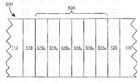
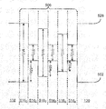
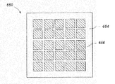
도 6a는 본 개시 내용의 방법의 실시 예에 따른 반도체 구조의 제조에 이용되는 성장 템플레이트를 제조하는 데 채택될 수 있는 중간 반도체 구조의 단순화된 상면도이다.
도 6b는 도 6a의 중간 반도체 구조의 부분 측단면도이다.
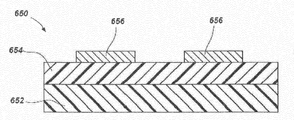
도 6c는 본 개시 내용의 방법의 실시 예에 따른 반도체 구조를 제조하는 데 채택될 수 있는 성장 템플레이트의 부분 측단면도이다.
도 6d는 도 6c의 것과 같은 성장 템플레이트 위에 에피택셜 증착되는 성장 스택(growth stack)의 층을 도시한다.
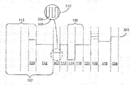
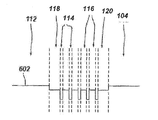
도 7은 본 개시 내용의 방법의 실시 예에 따른 반도체 구조로 제조되는 발광 장치의 부분 측단면도이다.
도 8은 본 개시 내용의 방법의 실시 예에 따른 반도체 구조로부터 제조되는 추가의 발광 장치의 부분 측단면도이다.
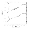
도 9는 본 개시 내용의 방법의 실시 예에 따라 형성되는 반도체 구조의 전체 변형 에너지와 내부 양자 효율(internal quantum efficiency) 간의 관계를 도시하는 그래프이다.
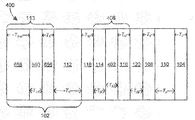
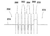
도 10a는 LED의 활성 영역에 InGaN 우물 층 및 GaN 배리어 층을 포함하는 이미 알려진 LED의 단순화된 측면도이다.
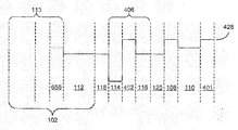
도 10b는 도 10a의 LED에 대한 단순화된 전도대 다이어그램이다.
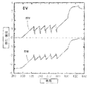
도 11a는 도 10a의 LED의 활성 영역 양단에 제로 인가 전압에 의한 가전자대(valence band) 및 전도대에 대한 계산된 밴드 에지를 도시하는 그래프이고, 계산은 LED의 계산 모델을 이용하여 얻어진다.
도 11b는 도 11a의 것과 유사하지만, 활성 영역의 인가 전압으로 인한 LED의 활성 영역을 가로질러 흐르는 125 A/cm2의 전류 밀도를 갖는 가전자대 및 전도대에 대한 계산된 밴드 에지를 도시하는 그래프이다.
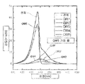
도 11c는 도 11a의 LED에서 각각의 InGaN 양자 우물 층에 대한 파장의 함수로서 방출 방사선의 계산된 강도를 도시하는 그래프이다.
도 11d는 도 11a의 LED의 활성 영역에 걸쳐 인가된 전류 밀도의 함수로서 계산된 캐리어 주입 효율을 도시하는 그래프이다.
도 12a는 도 1a의 것과 유사하고 LED의 활성 영역에 InGaN 우물 층 및 InGaN 배리어 층을 포함하는 본 개시 내용의 LED의 단순화된 측면도이다.
도 12b는 도 12a의 LED의 단순화된 전도대 다이어그램이다.
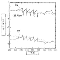
도 13a는 도 12a의 LED의 활성 영역에 걸친 제로 인가 전압을 갖는 가전자대 및 전도대에 대한 계산된 밴드 에지를 도시하는 그래프이고, 계산은 LED의 계산 모델을 이용하여 얻어진다.
도 13b는 도 13a와 유사하지만, 활성 영역 양단의 인가 전압으로 인해 LED의 활성 영역을 가로질러 흐르는 125 A/cm2의 전류 밀도를 갖는 가전자대 및 전도대에 대한 계산된 밴드 에지를 도시하는 그래프이다.
도 13c는 도 13a의 LED에서 각각의 InGaN 양자 우물 층에 대한 파장의 함수로서 방출 방사선의 계산된 강도를 도시하는 그래프이다.
도 13d는 도 13a의 LED의 활성 영역에 걸친 인가된 전류 밀도의 함수로서 계산된 캐리어 주입 효율을 도시하는 그래프이다.
도 13e는 도 13a의 LED의 활성 영역에 걸친 계산된 전류 밀도의 함수로서 계산된 내부 양자 효율을 도시하는 그래프이다.
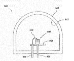
도 14는 본 개시 내용의 LED를 포함하는 발광 장치의 예를 도시한다.

| QW1 | QW2 | QW3 | QW4 | QW5 | |
| 파동 함수 오버랩 | 0.328 | 0.326 | 0.325 | 0.341 | 0.362 |
| 피크 방사 재결합 레이트 | 6.5e26 | 3.3e26 | 3.3e26 | 6.8e26 | 2.4e27 |
| QW1 | QW2 | QW3 | QW4 | QW5 | |
| 파동 함수 오버랩 | 0.478 | 0.493 | 0.494 | 0.494 | 0.471 |
| 피크 방사 재결합 레이트 | 7.8e26 | 7.7e26 | 7.9e26 | 8.1e26 | 8.3e26 |

Claims (15)
- 반도체 구조에 있어서,
약 3.189 옹스트롬보다 크거나 같은 성장 평면 격자 파라미터(growth plane lattice parameter)를 갖는 극성 성장 평면(polar growth plane)을 가지는 GaN 베이스 층(base layer);
상기 베이스 층 위에 배치되며, 적어도 하나의 InwGa1 - wN 우물 층, 및 적어도 하나의 InbGa1 - bN 배리어 층을 포함하는 복수의 InGaN의 층을 포함하고, 상기 w는 0.10≤w≤0.40이고, 상기 b는 0.01≤b≤0.10인 활성 영역(active region);
상기 GaN 베이스 층과 반대측인 상기 활성 영역 위에 배치되는 전자 차단 층(electron blocking layer);
상기 전자 차단 층 위에 배치되며, InpGa1-pN을 포함하고, 상기 p는 0.00≤p≤0.08인 p-형 벌크 층(p-type bulk layer); 및
상기 p-형 벌크 층 상에 배치되며, IncGa1-cN을 포함하고, 상기 c는 0.00≤c≤0.10인 p-형 접촉 층(p-type contact layer);을 포함하는 반도체 구조. - 제 1 항에 있어서,
상기 베이스 층은 성장 템플레이트(growth template)를 더 포함하고, 상기 성장 템플레이트는:
지지 기판; 및
상기 지지 기판 위에 배치되며, 성장 평면은 약 3.189 옹스트롬보다 크거나 같은 성장 평면 격자 파라미터를 갖는 극평면(polar plane)인 InsGa1 - sN 시드 층(seed layer);을 포함하고, 상기 s는 0.02≤s≤0.05이고, 상기 GaN 베이스 층은, 상기 InsGa1 - sN 시드 층의 상기 성장 평면과 실질적으로 매칭되는 격자(lattice)인 반도체 구조. - 제 1 항에 있어서,
상기 전자 차단 층은, 적어도 실질적으로 GaN으로 구성되는 반도체 구조. - 제 1 항에 있어서,
상기 GaN 베이스 층과 상기 활성 영역 사이에 배치되는 전자 정지 층(electron stopping layer);을 더 포함하고, 상기 전자 정지 층은 AlstGa1 -stN을 포함하고, 상기 st는 0.01≤st≤0.20인 반도체 구조. - 제 1 항에 있어서,
상기 GaN 베이스 층과 상기 활성 영역 사이에 배치되는 변형 완화 층(strain relief layer);을 더 포함하고,
상기 변형 완화 층은, InsraGasraN와 InsrbGa-1srbN 의 교대 층(alternating layers)을 포함하는 초격자 구조(superlattice structure)를 가지며, 상기 sra는 0.01≤sra≤0.10, 상기 srb는 0.01≤srb≤0.10이고, 상기 sra는 srb보다 큰 반도체 구조. - 제 1 항에 있어서,
상기 활성 영역은, 상기 적어도 하나의 우물 층과 상기 적어도 하나의 배리어 층 사이에 배치되며, GaN을 포함하는 추가의 배리어 층(additional barrier layer)을 더 포함하는 반도체 구조. - 제 1 항에 있어서,
상기 반도체 구조의 임계 변형 에너지(critical strain energy)는, 각각의 층 두께(nm)와 각각의 층의 인듐 함량(%)의 곱(product)의 합(sum)으로 정의되고, 4500이하인 반도체 구조. - 제 1 항에 있어서,
상기 p-형 접촉 층은, 적어도 실질적으로 GaN으로 구성되는 반도체 구조. - 반도체 구조를 형성하는 방법에 있어서,
약 3.189 Å보다 크거나 같은 성장 평면 격자 파라미터를 갖는 극성 성장 평면을 가지는 GaN 베이스 층을 제공하는 단계;
활성 영역을 형성하기 위해 상기 베이스 층 위에 복수의 InGaN의 층을 성장시키는 단계;
상기 활성 영역 위에 전자 차단 층을 성장시키는 단계;
상기 전자 차단 층 위에 p-형 InpGa1-pN 벌크 층을 성장시키는 단계; 및
상기 p-형 InpGa1 - pN 벌크 층 위에 p-형 IncGa1 - cN 접촉 층을 성장시키는 단계;를 포함하고,
상기 p는 0.00≤p≤0.08, 상기 c는 0.00≤c≤0.10이며,
상기 복수의 InGaN의 층을 성장시키는 단계는,
적어도 하나의 InwGa1-wN 우물 층을 성장시키는 단계, 및
상기 적어도 하나의 우물 층 위에 적어도 하나의 InbGa1 - bN 배리어 층을 성장시키는 단계를 포함하고, 상기 w는 0.10≤w≤0.40, 상기 b는 0.01≤b≤0.10인 반도체 구조 형성 방법. - 제 9 항에 있어서,
상기 베이스 층을 형성하는 단계는, 성장 템플레이트를 형성하는 단계를 더 포함하고,
상기 성장 템플레이트를 형성하는 단계는:
지지 기판을 제공하는 단계, 및
InsGa1 - sN 시드 층을 상기 지지 기판에 접합하는 단계를 포함하고, 상기 InsGa1-sN 시드 층의 성장 평면은, 약 3.189 옹스트롬보다 크거나 같은 성장 평면 격자 파라미터를 갖는 극평면이고, 상기 InsGa1 - sN 시드 층에서 상기 s는 0.02≤s≤0.05 인 반도체 구조 형성 방법. - 제 9 항에 있어서,
상기 전자 차단 층을 성장시키는 단계는, 적어도 실질적으로 GaN으로 구성된 상기 전자 차단 층을 성장시키는 단계를 포함하는 반도체 구조 형성 방법. - 제 9 항에 있어서,
상기 GaN 베이스 층과 상기 활성 영역 사이에 배치되는 전자 정지 층을 성장시키는 단계;를 더 포함하고,
상기 전자 정지 층은, 적어도 실질적으로 AlstGa1 -stN으로 구성되고, 상기 st는 0.01≤st≤0.20인 반도체 구조 형성 방법. - 제 9 항에 있어서,
상기 GaN 베이스 층과 상기 활성 영역 사이에 배치되는 변형 완화 층을 성장시키는 단계;를 더 포함하고,
상기 변형 완화 층은, InsraGasraN 와 InsrbGa-1srbN 의 교대 층을 포함하는 초격자 구조를 가지며, 상기 sra는 0.01≤sra≤0.10, 상기 srb는 0.01≤srb≤0.10이고, 상기 sra는 srb보다 큰 반도체 구조 형성 방법. - 제 9 항에 있어서,
각각의 층 두께(nm)와 각각의 층의 인듐 함량(%)의 곱의 합에 의해 정의되고, 2800과 같거나 작은 임계 변형 에너지를 가지도록 상기 반도체 구조를 형성하는 단계;를 더 포함하는 반도체 구조 형성 방법. - 제 9 항에 있어서,
상기 p-형 접촉 층을 성장시키는 단계는, 적어도 실질적으로 GaN으로 구성된 상기 p-형 접촉 층을 성장시키는 단계를 포함하는 반도체 구조 형성 방법.
Applications Claiming Priority (13)
| Application Number | Priority Date | Filing Date | Title |
|---|---|---|---|
| US201361790085P | 2013-03-15 | 2013-03-15 | |
| US201361789792P | 2013-03-15 | 2013-03-15 | |
| US201361788441P | 2013-03-15 | 2013-03-15 | |
| US61/789,792 | 2013-03-15 | ||
| US61/790,085 | 2013-03-15 | ||
| US61/788,441 | 2013-03-15 | ||
| FR1300823 | 2013-04-08 | ||
| FR1300823A FR3003397B1 (fr) | 2013-03-15 | 2013-04-08 | Structures semi-conductrices dotées de régions actives comprenant de l'INGAN |
| FR1300860 | 2013-04-11 | ||
| FR1300860A FR3003396B1 (fr) | 2013-03-15 | 2013-04-11 | Structures semi-conductrices dotees de regions actives comprenant de l'ingan |
| FR1300923A FR3004585B1 (fr) | 2013-04-12 | 2013-04-12 | Structures semi-conductrices dotees de regions actives comprenant de l'ingan |
| FR1300923 | 2013-04-12 | ||
| PCT/EP2014/055316 WO2014140371A1 (en) | 2013-03-15 | 2014-03-17 | Semiconductor structures having active regions comprising ingan, methods of forming such semiconductor structures, and light emitting devices formed from such semiconductor structures |
Publications (1)
| Publication Number | Publication Date |
|---|---|
| KR20150132204A true KR20150132204A (ko) | 2015-11-25 |
Family
ID=50288078
Family Applications (3)
| Application Number | Title | Priority Date | Filing Date |
|---|---|---|---|
| KR1020157026743A KR20150132204A (ko) | 2013-03-15 | 2014-03-17 | InGaN을 포함하는 활성 영역을 가지는 반도체 구조, 그와 같은 반도체 구조를 형성하는 방법, 및 그와 같은 반도체 구조로부터 형성되는 발광 장치 |
| KR1020157026564A KR20150130331A (ko) | 2013-03-15 | 2014-03-17 | Ingan을 포함하는 활성 영역을 가지는 발광 다이오드 반도체 구조 |
| KR1020157026427A KR102120682B1 (ko) | 2013-03-15 | 2014-03-17 | InGaN을 포함하는 활성 영역을 가지는 반도체 구조, 그와 같은 반도체 구조를 형성하는 방법, 및 그와 같은 반도체 구조로부터 형성되는 발광 장치 |
Family Applications After (2)
| Application Number | Title | Priority Date | Filing Date |
|---|---|---|---|
| KR1020157026564A KR20150130331A (ko) | 2013-03-15 | 2014-03-17 | Ingan을 포함하는 활성 영역을 가지는 발광 다이오드 반도체 구조 |
| KR1020157026427A KR102120682B1 (ko) | 2013-03-15 | 2014-03-17 | InGaN을 포함하는 활성 영역을 가지는 반도체 구조, 그와 같은 반도체 구조를 형성하는 방법, 및 그와 같은 반도체 구조로부터 형성되는 발광 장치 |
Country Status (1)
| Country | Link |
|---|---|
| KR (3) | KR20150132204A (ko) |
Families Citing this family (1)
| Publication number | Priority date | Publication date | Assignee | Title |
|---|---|---|---|---|
| KR102653003B1 (ko) * | 2018-06-29 | 2024-04-01 | 쑤저우 레킨 세미컨덕터 컴퍼니 리미티드 | 반도체 소자 |
Family Cites Families (3)
| Publication number | Priority date | Publication date | Assignee | Title |
|---|---|---|---|---|
| JP4441563B2 (ja) * | 2000-12-28 | 2010-03-31 | 日亜化学工業株式会社 | 窒化物半導体レーザ素子 |
| KR100525545B1 (ko) * | 2003-06-25 | 2005-10-31 | 엘지이노텍 주식회사 | 질화물 반도체 발광소자 및 그 제조방법 |
| JP2013502731A (ja) * | 2009-08-21 | 2013-01-24 | ザ リージェンツ オブ ザ ユニバーシティ オブ カリフォルニア | ミスフィット転位を有する部分的または完全に弛緩したAlInGaN層による半極性窒化物量子井戸の異方性ひずみ制御 |
-
2014
- 2014-03-17 KR KR1020157026743A patent/KR20150132204A/ko not_active Application Discontinuation
- 2014-03-17 KR KR1020157026564A patent/KR20150130331A/ko not_active Application Discontinuation
- 2014-03-17 KR KR1020157026427A patent/KR102120682B1/ko active IP Right Grant
Also Published As
| Publication number | Publication date |
|---|---|
| KR102120682B1 (ko) | 2020-06-17 |
| KR20150130331A (ko) | 2015-11-23 |
| KR20150132199A (ko) | 2015-11-25 |
Similar Documents
| Publication | Publication Date | Title |
|---|---|---|
| US9978905B2 (en) | Semiconductor structures having active regions comprising InGaN and methods of forming such semiconductor structures | |
| US9397258B2 (en) | Semiconductor structures having active regions comprising InGaN, methods of forming such semiconductor structures, and light emitting devices formed from such semiconductor structures | |
| US9634182B2 (en) | Semiconductor structures having active regions including indium gallium nitride, methods of forming such semiconductor structures, and related light emitting devices | |
| TWI451591B (zh) | 以氮化物為主之發光裝置 | |
| CN103578926B (zh) | 半导体缓冲结构、半导体器件和制造半导体器件的方法 | |
| So et al. | Improved carrier injection of AlGaN-based deep ultraviolet light emitting diodes with graded superlattice electron blocking layers | |
| CN104272477B (zh) | 氮化物半导体发光元件 | |
| WO2014140371A1 (en) | Semiconductor structures having active regions comprising ingan, methods of forming such semiconductor structures, and light emitting devices formed from such semiconductor structures | |
| CN106415860A (zh) | 氮化物半导体发光元件 | |
| EP2693499B1 (en) | Semiconductor light emitting device and method for manufacturing the same | |
| KR102120682B1 (ko) | InGaN을 포함하는 활성 영역을 가지는 반도체 구조, 그와 같은 반도체 구조를 형성하는 방법, 및 그와 같은 반도체 구조로부터 형성되는 발광 장치 | |
| KR101198759B1 (ko) | 질화물계 발광 소자 | |
| JP6356530B2 (ja) | 窒化物半導体発光素子及びその製造方法 | |
| KR100809226B1 (ko) | 질화물 반도체 발광 소자 및 제조방법 | |
| JP2008227103A (ja) | GaN系半導体発光素子 | |
| TWI626765B (zh) | 具有包含InGaN之作用區域之半導體結構、形成此等半導體結構之方法及由此等半導體結構所形成之發光裝置 | |
| KR101018760B1 (ko) | 반도체 기판과 이의 제조 방법 | |
| KR101875231B1 (ko) | 질화물계 발광소자 및 그 제조방법 | |
| JP2014112599A (ja) | 半導体発光素子及びその製造方法 |
Legal Events
| Date | Code | Title | Description |
|---|---|---|---|
| PA0105 | International application |
Patent event date: 20150925 Patent event code: PA01051R01D Comment text: International Patent Application |
|
| PG1501 | Laying open of application | ||
| A201 | Request for examination | ||
| PA0201 | Request for examination |
Patent event code: PA02012R01D Patent event date: 20190128 Comment text: Request for Examination of Application |
|
| E902 | Notification of reason for refusal | ||
| PE0902 | Notice of grounds for rejection |
Comment text: Notification of reason for refusal Patent event date: 20200120 Patent event code: PE09021S01D |
|
| E601 | Decision to refuse application | ||
| PE0601 | Decision on rejection of patent |
Patent event date: 20200507 Comment text: Decision to Refuse Application Patent event code: PE06012S01D Patent event date: 20200120 Comment text: Notification of reason for refusal Patent event code: PE06011S01I |