KR20150067636A - Liquid crystal display device and manufacturing method thereof - Google Patents
Liquid crystal display device and manufacturing method thereof Download PDFInfo
- Publication number
- KR20150067636A KR20150067636A KR1020130153341A KR20130153341A KR20150067636A KR 20150067636 A KR20150067636 A KR 20150067636A KR 1020130153341 A KR1020130153341 A KR 1020130153341A KR 20130153341 A KR20130153341 A KR 20130153341A KR 20150067636 A KR20150067636 A KR 20150067636A
- Authority
- KR
- South Korea
- Prior art keywords
- substrate
- liquid crystal
- crystal display
- layer
- polarizing plate
- Prior art date
Links
- 239000004973 liquid crystal related substance Substances 0.000 title claims abstract description 196
- 238000004519 manufacturing process Methods 0.000 title description 12
- 239000000758 substrate Substances 0.000 claims abstract description 107
- 238000002347 injection Methods 0.000 claims abstract description 30
- 239000007924 injection Substances 0.000 claims abstract description 30
- 230000010287 polarization Effects 0.000 claims abstract description 28
- 239000010409 thin film Substances 0.000 claims abstract description 26
- 239000010410 layer Substances 0.000 claims description 174
- 239000000463 material Substances 0.000 claims description 30
- 238000000034 method Methods 0.000 claims description 29
- 239000000853 adhesive Substances 0.000 claims description 25
- 230000001070 adhesive effect Effects 0.000 claims description 24
- 239000012790 adhesive layer Substances 0.000 claims description 22
- 239000013039 cover film Substances 0.000 claims description 13
- 238000010438 heat treatment Methods 0.000 claims description 12
- 239000011368 organic material Substances 0.000 claims description 12
- -1 polyethylene terephthalate Polymers 0.000 claims description 9
- 229920002284 Cellulose triacetate Polymers 0.000 claims description 8
- NNLVGZFZQQXQNW-ADJNRHBOSA-N [(2r,3r,4s,5r,6s)-4,5-diacetyloxy-3-[(2s,3r,4s,5r,6r)-3,4,5-triacetyloxy-6-(acetyloxymethyl)oxan-2-yl]oxy-6-[(2r,3r,4s,5r,6s)-4,5,6-triacetyloxy-2-(acetyloxymethyl)oxan-3-yl]oxyoxan-2-yl]methyl acetate Chemical compound O([C@@H]1O[C@@H]([C@H]([C@H](OC(C)=O)[C@H]1OC(C)=O)O[C@H]1[C@@H]([C@@H](OC(C)=O)[C@H](OC(C)=O)[C@@H](COC(C)=O)O1)OC(C)=O)COC(=O)C)[C@@H]1[C@@H](COC(C)=O)O[C@@H](OC(C)=O)[C@H](OC(C)=O)[C@H]1OC(C)=O NNLVGZFZQQXQNW-ADJNRHBOSA-N 0.000 claims description 8
- 229920000139 polyethylene terephthalate Polymers 0.000 claims description 8
- 239000005020 polyethylene terephthalate Substances 0.000 claims description 8
- 229920002554 vinyl polymer Polymers 0.000 claims description 4
- 239000004065 semiconductor Substances 0.000 description 37
- 239000010408 film Substances 0.000 description 27
- VYPSYNLAJGMNEJ-UHFFFAOYSA-N Silicium dioxide Chemical compound O=[Si]=O VYPSYNLAJGMNEJ-UHFFFAOYSA-N 0.000 description 14
- 229910052814 silicon oxide Inorganic materials 0.000 description 14
- 238000005452 bending Methods 0.000 description 13
- 229910052581 Si3N4 Inorganic materials 0.000 description 12
- 239000011810 insulating material Substances 0.000 description 12
- HQVNEWCFYHHQES-UHFFFAOYSA-N silicon nitride Chemical compound N12[Si]34N5[Si]62N3[Si]51N64 HQVNEWCFYHHQES-UHFFFAOYSA-N 0.000 description 12
- 229910004205 SiNX Inorganic materials 0.000 description 7
- 230000000052 comparative effect Effects 0.000 description 6
- 239000004020 conductor Substances 0.000 description 6
- 230000006837 decompression Effects 0.000 description 6
- 230000005684 electric field Effects 0.000 description 6
- 230000001681 protective effect Effects 0.000 description 6
- 230000000007 visual effect Effects 0.000 description 6
- 229910020286 SiOxNy Inorganic materials 0.000 description 5
- 239000007769 metal material Substances 0.000 description 5
- 229920002120 photoresistant polymer Polymers 0.000 description 5
- 239000003086 colorant Substances 0.000 description 4
- AMGQUBHHOARCQH-UHFFFAOYSA-N indium;oxotin Chemical compound [In].[Sn]=O AMGQUBHHOARCQH-UHFFFAOYSA-N 0.000 description 4
- 239000007788 liquid Substances 0.000 description 4
- 238000002161 passivation Methods 0.000 description 4
- 238000000059 patterning Methods 0.000 description 4
- YVTHLONGBIQYBO-UHFFFAOYSA-N zinc indium(3+) oxygen(2-) Chemical compound [O--].[Zn++].[In+3] YVTHLONGBIQYBO-UHFFFAOYSA-N 0.000 description 4
- 229910021417 amorphous silicon Inorganic materials 0.000 description 3
- 238000009413 insulation Methods 0.000 description 3
- 239000002159 nanocrystal Substances 0.000 description 3
- 239000003990 capacitor Substances 0.000 description 2
- 230000008878 coupling Effects 0.000 description 2
- 238000010168 coupling process Methods 0.000 description 2
- 238000005859 coupling reaction Methods 0.000 description 2
- 239000011521 glass Substances 0.000 description 2
- 229910044991 metal oxide Inorganic materials 0.000 description 2
- 150000004706 metal oxides Chemical class 0.000 description 2
- 238000012986 modification Methods 0.000 description 2
- 230000004048 modification Effects 0.000 description 2
- 238000000206 photolithography Methods 0.000 description 2
- 239000004033 plastic Substances 0.000 description 2
- 229920003023 plastic Polymers 0.000 description 2
- 229910021420 polycrystalline silicon Inorganic materials 0.000 description 2
- 238000007789 sealing Methods 0.000 description 2
- 239000002356 single layer Substances 0.000 description 2
- 239000000243 solution Substances 0.000 description 2
- 239000004642 Polyimide Substances 0.000 description 1
- 238000004380 ashing Methods 0.000 description 1
- 238000010586 diagram Methods 0.000 description 1
- 239000007772 electrode material Substances 0.000 description 1
- 238000005530 etching Methods 0.000 description 1
- 239000012535 impurity Substances 0.000 description 1
- 230000001678 irradiating effect Effects 0.000 description 1
- 239000011159 matrix material Substances 0.000 description 1
- 229920005575 poly(amic acid) Polymers 0.000 description 1
- 229920000052 poly(p-xylylene) Polymers 0.000 description 1
- 229920001721 polyimide Polymers 0.000 description 1
- 229920001296 polysiloxane Polymers 0.000 description 1
- 229910021332 silicide Inorganic materials 0.000 description 1
- FVBUAEGBCNSCDD-UHFFFAOYSA-N silicide(4-) Chemical compound [Si-4] FVBUAEGBCNSCDD-UHFFFAOYSA-N 0.000 description 1
- 238000004528 spin coating Methods 0.000 description 1
Images


Classifications
-
- G—PHYSICS
- G02—OPTICS
- G02F—OPTICAL DEVICES OR ARRANGEMENTS FOR THE CONTROL OF LIGHT BY MODIFICATION OF THE OPTICAL PROPERTIES OF THE MEDIA OF THE ELEMENTS INVOLVED THEREIN; NON-LINEAR OPTICS; FREQUENCY-CHANGING OF LIGHT; OPTICAL LOGIC ELEMENTS; OPTICAL ANALOGUE/DIGITAL CONVERTERS
- G02F1/00—Devices or arrangements for the control of the intensity, colour, phase, polarisation or direction of light arriving from an independent light source, e.g. switching, gating or modulating; Non-linear optics
- G02F1/01—Devices or arrangements for the control of the intensity, colour, phase, polarisation or direction of light arriving from an independent light source, e.g. switching, gating or modulating; Non-linear optics for the control of the intensity, phase, polarisation or colour
- G02F1/13—Devices or arrangements for the control of the intensity, colour, phase, polarisation or direction of light arriving from an independent light source, e.g. switching, gating or modulating; Non-linear optics for the control of the intensity, phase, polarisation or colour based on liquid crystals, e.g. single liquid crystal display cells
- G02F1/133—Constructional arrangements; Operation of liquid crystal cells; Circuit arrangements
- G02F1/1333—Constructional arrangements; Manufacturing methods
- G02F1/1335—Structural association of cells with optical devices, e.g. polarisers or reflectors
- G02F1/133528—Polarisers
-
- G—PHYSICS
- G02—OPTICS
- G02F—OPTICAL DEVICES OR ARRANGEMENTS FOR THE CONTROL OF LIGHT BY MODIFICATION OF THE OPTICAL PROPERTIES OF THE MEDIA OF THE ELEMENTS INVOLVED THEREIN; NON-LINEAR OPTICS; FREQUENCY-CHANGING OF LIGHT; OPTICAL LOGIC ELEMENTS; OPTICAL ANALOGUE/DIGITAL CONVERTERS
- G02F1/00—Devices or arrangements for the control of the intensity, colour, phase, polarisation or direction of light arriving from an independent light source, e.g. switching, gating or modulating; Non-linear optics
- G02F1/01—Devices or arrangements for the control of the intensity, colour, phase, polarisation or direction of light arriving from an independent light source, e.g. switching, gating or modulating; Non-linear optics for the control of the intensity, phase, polarisation or colour
- G02F1/13—Devices or arrangements for the control of the intensity, colour, phase, polarisation or direction of light arriving from an independent light source, e.g. switching, gating or modulating; Non-linear optics for the control of the intensity, phase, polarisation or colour based on liquid crystals, e.g. single liquid crystal display cells
- G02F1/133—Constructional arrangements; Operation of liquid crystal cells; Circuit arrangements
- G02F1/136—Liquid crystal cells structurally associated with a semi-conducting layer or substrate, e.g. cells forming part of an integrated circuit
- G02F1/1362—Active matrix addressed cells
-
- G—PHYSICS
- G02—OPTICS
- G02F—OPTICAL DEVICES OR ARRANGEMENTS FOR THE CONTROL OF LIGHT BY MODIFICATION OF THE OPTICAL PROPERTIES OF THE MEDIA OF THE ELEMENTS INVOLVED THEREIN; NON-LINEAR OPTICS; FREQUENCY-CHANGING OF LIGHT; OPTICAL LOGIC ELEMENTS; OPTICAL ANALOGUE/DIGITAL CONVERTERS
- G02F1/00—Devices or arrangements for the control of the intensity, colour, phase, polarisation or direction of light arriving from an independent light source, e.g. switching, gating or modulating; Non-linear optics
- G02F1/01—Devices or arrangements for the control of the intensity, colour, phase, polarisation or direction of light arriving from an independent light source, e.g. switching, gating or modulating; Non-linear optics for the control of the intensity, phase, polarisation or colour
- G02F1/13—Devices or arrangements for the control of the intensity, colour, phase, polarisation or direction of light arriving from an independent light source, e.g. switching, gating or modulating; Non-linear optics for the control of the intensity, phase, polarisation or colour based on liquid crystals, e.g. single liquid crystal display cells
- G02F1/133—Constructional arrangements; Operation of liquid crystal cells; Circuit arrangements
- G02F1/1333—Constructional arrangements; Manufacturing methods
- G02F1/133377—Cells with plural compartments or having plurality of liquid crystal microcells partitioned by walls, e.g. one microcell per pixel
-
- G—PHYSICS
- G02—OPTICS
- G02F—OPTICAL DEVICES OR ARRANGEMENTS FOR THE CONTROL OF LIGHT BY MODIFICATION OF THE OPTICAL PROPERTIES OF THE MEDIA OF THE ELEMENTS INVOLVED THEREIN; NON-LINEAR OPTICS; FREQUENCY-CHANGING OF LIGHT; OPTICAL LOGIC ELEMENTS; OPTICAL ANALOGUE/DIGITAL CONVERTERS
- G02F1/00—Devices or arrangements for the control of the intensity, colour, phase, polarisation or direction of light arriving from an independent light source, e.g. switching, gating or modulating; Non-linear optics
- G02F1/01—Devices or arrangements for the control of the intensity, colour, phase, polarisation or direction of light arriving from an independent light source, e.g. switching, gating or modulating; Non-linear optics for the control of the intensity, phase, polarisation or colour
- G02F1/13—Devices or arrangements for the control of the intensity, colour, phase, polarisation or direction of light arriving from an independent light source, e.g. switching, gating or modulating; Non-linear optics for the control of the intensity, phase, polarisation or colour based on liquid crystals, e.g. single liquid crystal display cells
- G02F1/133—Constructional arrangements; Operation of liquid crystal cells; Circuit arrangements
- G02F1/1333—Constructional arrangements; Manufacturing methods
- G02F1/1335—Structural association of cells with optical devices, e.g. polarisers or reflectors
-
- G—PHYSICS
- G02—OPTICS
- G02F—OPTICAL DEVICES OR ARRANGEMENTS FOR THE CONTROL OF LIGHT BY MODIFICATION OF THE OPTICAL PROPERTIES OF THE MEDIA OF THE ELEMENTS INVOLVED THEREIN; NON-LINEAR OPTICS; FREQUENCY-CHANGING OF LIGHT; OPTICAL LOGIC ELEMENTS; OPTICAL ANALOGUE/DIGITAL CONVERTERS
- G02F1/00—Devices or arrangements for the control of the intensity, colour, phase, polarisation or direction of light arriving from an independent light source, e.g. switching, gating or modulating; Non-linear optics
- G02F1/01—Devices or arrangements for the control of the intensity, colour, phase, polarisation or direction of light arriving from an independent light source, e.g. switching, gating or modulating; Non-linear optics for the control of the intensity, phase, polarisation or colour
- G02F1/13—Devices or arrangements for the control of the intensity, colour, phase, polarisation or direction of light arriving from an independent light source, e.g. switching, gating or modulating; Non-linear optics for the control of the intensity, phase, polarisation or colour based on liquid crystals, e.g. single liquid crystal display cells
- G02F1/133—Constructional arrangements; Operation of liquid crystal cells; Circuit arrangements
- G02F1/1333—Constructional arrangements; Manufacturing methods
- G02F1/1341—Filling or closing of cells
-
- G—PHYSICS
- G02—OPTICS
- G02F—OPTICAL DEVICES OR ARRANGEMENTS FOR THE CONTROL OF LIGHT BY MODIFICATION OF THE OPTICAL PROPERTIES OF THE MEDIA OF THE ELEMENTS INVOLVED THEREIN; NON-LINEAR OPTICS; FREQUENCY-CHANGING OF LIGHT; OPTICAL LOGIC ELEMENTS; OPTICAL ANALOGUE/DIGITAL CONVERTERS
- G02F1/00—Devices or arrangements for the control of the intensity, colour, phase, polarisation or direction of light arriving from an independent light source, e.g. switching, gating or modulating; Non-linear optics
- G02F1/01—Devices or arrangements for the control of the intensity, colour, phase, polarisation or direction of light arriving from an independent light source, e.g. switching, gating or modulating; Non-linear optics for the control of the intensity, phase, polarisation or colour
- G02F1/13—Devices or arrangements for the control of the intensity, colour, phase, polarisation or direction of light arriving from an independent light source, e.g. switching, gating or modulating; Non-linear optics for the control of the intensity, phase, polarisation or colour based on liquid crystals, e.g. single liquid crystal display cells
- G02F1/133—Constructional arrangements; Operation of liquid crystal cells; Circuit arrangements
- G02F1/1333—Constructional arrangements; Manufacturing methods
- G02F1/1343—Electrodes
- G02F1/134309—Electrodes characterised by their geometrical arrangement
- G02F1/134336—Matrix
-
- G—PHYSICS
- G02—OPTICS
- G02F—OPTICAL DEVICES OR ARRANGEMENTS FOR THE CONTROL OF LIGHT BY MODIFICATION OF THE OPTICAL PROPERTIES OF THE MEDIA OF THE ELEMENTS INVOLVED THEREIN; NON-LINEAR OPTICS; FREQUENCY-CHANGING OF LIGHT; OPTICAL LOGIC ELEMENTS; OPTICAL ANALOGUE/DIGITAL CONVERTERS
- G02F1/00—Devices or arrangements for the control of the intensity, colour, phase, polarisation or direction of light arriving from an independent light source, e.g. switching, gating or modulating; Non-linear optics
- G02F1/01—Devices or arrangements for the control of the intensity, colour, phase, polarisation or direction of light arriving from an independent light source, e.g. switching, gating or modulating; Non-linear optics for the control of the intensity, phase, polarisation or colour
- G02F1/13—Devices or arrangements for the control of the intensity, colour, phase, polarisation or direction of light arriving from an independent light source, e.g. switching, gating or modulating; Non-linear optics for the control of the intensity, phase, polarisation or colour based on liquid crystals, e.g. single liquid crystal display cells
- G02F1/133—Constructional arrangements; Operation of liquid crystal cells; Circuit arrangements
- G02F1/136—Liquid crystal cells structurally associated with a semi-conducting layer or substrate, e.g. cells forming part of an integrated circuit
- G02F1/1362—Active matrix addressed cells
- G02F1/1368—Active matrix addressed cells in which the switching element is a three-electrode device
-
- G—PHYSICS
- G02—OPTICS
- G02F—OPTICAL DEVICES OR ARRANGEMENTS FOR THE CONTROL OF LIGHT BY MODIFICATION OF THE OPTICAL PROPERTIES OF THE MEDIA OF THE ELEMENTS INVOLVED THEREIN; NON-LINEAR OPTICS; FREQUENCY-CHANGING OF LIGHT; OPTICAL LOGIC ELEMENTS; OPTICAL ANALOGUE/DIGITAL CONVERTERS
- G02F1/00—Devices or arrangements for the control of the intensity, colour, phase, polarisation or direction of light arriving from an independent light source, e.g. switching, gating or modulating; Non-linear optics
- G02F1/01—Devices or arrangements for the control of the intensity, colour, phase, polarisation or direction of light arriving from an independent light source, e.g. switching, gating or modulating; Non-linear optics for the control of the intensity, phase, polarisation or colour
- G02F1/13—Devices or arrangements for the control of the intensity, colour, phase, polarisation or direction of light arriving from an independent light source, e.g. switching, gating or modulating; Non-linear optics for the control of the intensity, phase, polarisation or colour based on liquid crystals, e.g. single liquid crystal display cells
- G02F1/133—Constructional arrangements; Operation of liquid crystal cells; Circuit arrangements
- G02F1/1333—Constructional arrangements; Manufacturing methods
- G02F1/133345—Insulating layers
-
- G—PHYSICS
- G02—OPTICS
- G02F—OPTICAL DEVICES OR ARRANGEMENTS FOR THE CONTROL OF LIGHT BY MODIFICATION OF THE OPTICAL PROPERTIES OF THE MEDIA OF THE ELEMENTS INVOLVED THEREIN; NON-LINEAR OPTICS; FREQUENCY-CHANGING OF LIGHT; OPTICAL LOGIC ELEMENTS; OPTICAL ANALOGUE/DIGITAL CONVERTERS
- G02F1/00—Devices or arrangements for the control of the intensity, colour, phase, polarisation or direction of light arriving from an independent light source, e.g. switching, gating or modulating; Non-linear optics
- G02F1/01—Devices or arrangements for the control of the intensity, colour, phase, polarisation or direction of light arriving from an independent light source, e.g. switching, gating or modulating; Non-linear optics for the control of the intensity, phase, polarisation or colour
- G02F1/13—Devices or arrangements for the control of the intensity, colour, phase, polarisation or direction of light arriving from an independent light source, e.g. switching, gating or modulating; Non-linear optics for the control of the intensity, phase, polarisation or colour based on liquid crystals, e.g. single liquid crystal display cells
- G02F1/133—Constructional arrangements; Operation of liquid crystal cells; Circuit arrangements
- G02F1/1333—Constructional arrangements; Manufacturing methods
- G02F1/1335—Structural association of cells with optical devices, e.g. polarisers or reflectors
- G02F1/133509—Filters, e.g. light shielding masks
- G02F1/133514—Colour filters
-
- G—PHYSICS
- G02—OPTICS
- G02F—OPTICAL DEVICES OR ARRANGEMENTS FOR THE CONTROL OF LIGHT BY MODIFICATION OF THE OPTICAL PROPERTIES OF THE MEDIA OF THE ELEMENTS INVOLVED THEREIN; NON-LINEAR OPTICS; FREQUENCY-CHANGING OF LIGHT; OPTICAL LOGIC ELEMENTS; OPTICAL ANALOGUE/DIGITAL CONVERTERS
- G02F1/00—Devices or arrangements for the control of the intensity, colour, phase, polarisation or direction of light arriving from an independent light source, e.g. switching, gating or modulating; Non-linear optics
- G02F1/01—Devices or arrangements for the control of the intensity, colour, phase, polarisation or direction of light arriving from an independent light source, e.g. switching, gating or modulating; Non-linear optics for the control of the intensity, phase, polarisation or colour
- G02F1/13—Devices or arrangements for the control of the intensity, colour, phase, polarisation or direction of light arriving from an independent light source, e.g. switching, gating or modulating; Non-linear optics for the control of the intensity, phase, polarisation or colour based on liquid crystals, e.g. single liquid crystal display cells
- G02F1/133—Constructional arrangements; Operation of liquid crystal cells; Circuit arrangements
- G02F1/1333—Constructional arrangements; Manufacturing methods
- G02F1/1335—Structural association of cells with optical devices, e.g. polarisers or reflectors
- G02F1/133528—Polarisers
- G02F1/133531—Polarisers characterised by the arrangement of polariser or analyser axes
-
- G—PHYSICS
- G02—OPTICS
- G02F—OPTICAL DEVICES OR ARRANGEMENTS FOR THE CONTROL OF LIGHT BY MODIFICATION OF THE OPTICAL PROPERTIES OF THE MEDIA OF THE ELEMENTS INVOLVED THEREIN; NON-LINEAR OPTICS; FREQUENCY-CHANGING OF LIGHT; OPTICAL LOGIC ELEMENTS; OPTICAL ANALOGUE/DIGITAL CONVERTERS
- G02F1/00—Devices or arrangements for the control of the intensity, colour, phase, polarisation or direction of light arriving from an independent light source, e.g. switching, gating or modulating; Non-linear optics
- G02F1/01—Devices or arrangements for the control of the intensity, colour, phase, polarisation or direction of light arriving from an independent light source, e.g. switching, gating or modulating; Non-linear optics for the control of the intensity, phase, polarisation or colour
- G02F1/13—Devices or arrangements for the control of the intensity, colour, phase, polarisation or direction of light arriving from an independent light source, e.g. switching, gating or modulating; Non-linear optics for the control of the intensity, phase, polarisation or colour based on liquid crystals, e.g. single liquid crystal display cells
- G02F1/133—Constructional arrangements; Operation of liquid crystal cells; Circuit arrangements
- G02F1/1333—Constructional arrangements; Manufacturing methods
- G02F1/1337—Surface-induced orientation of the liquid crystal molecules, e.g. by alignment layers
- G02F1/133711—Surface-induced orientation of the liquid crystal molecules, e.g. by alignment layers by organic films, e.g. polymeric films
-
- G—PHYSICS
- G02—OPTICS
- G02F—OPTICAL DEVICES OR ARRANGEMENTS FOR THE CONTROL OF LIGHT BY MODIFICATION OF THE OPTICAL PROPERTIES OF THE MEDIA OF THE ELEMENTS INVOLVED THEREIN; NON-LINEAR OPTICS; FREQUENCY-CHANGING OF LIGHT; OPTICAL LOGIC ELEMENTS; OPTICAL ANALOGUE/DIGITAL CONVERTERS
- G02F1/00—Devices or arrangements for the control of the intensity, colour, phase, polarisation or direction of light arriving from an independent light source, e.g. switching, gating or modulating; Non-linear optics
- G02F1/01—Devices or arrangements for the control of the intensity, colour, phase, polarisation or direction of light arriving from an independent light source, e.g. switching, gating or modulating; Non-linear optics for the control of the intensity, phase, polarisation or colour
- G02F1/13—Devices or arrangements for the control of the intensity, colour, phase, polarisation or direction of light arriving from an independent light source, e.g. switching, gating or modulating; Non-linear optics for the control of the intensity, phase, polarisation or colour based on liquid crystals, e.g. single liquid crystal display cells
- G02F1/133—Constructional arrangements; Operation of liquid crystal cells; Circuit arrangements
- G02F1/1333—Constructional arrangements; Manufacturing methods
- G02F1/1337—Surface-induced orientation of the liquid crystal molecules, e.g. by alignment layers
- G02F1/133742—Surface-induced orientation of the liquid crystal molecules, e.g. by alignment layers for homeotropic alignment
-
- G—PHYSICS
- G02—OPTICS
- G02F—OPTICAL DEVICES OR ARRANGEMENTS FOR THE CONTROL OF LIGHT BY MODIFICATION OF THE OPTICAL PROPERTIES OF THE MEDIA OF THE ELEMENTS INVOLVED THEREIN; NON-LINEAR OPTICS; FREQUENCY-CHANGING OF LIGHT; OPTICAL LOGIC ELEMENTS; OPTICAL ANALOGUE/DIGITAL CONVERTERS
- G02F1/00—Devices or arrangements for the control of the intensity, colour, phase, polarisation or direction of light arriving from an independent light source, e.g. switching, gating or modulating; Non-linear optics
- G02F1/01—Devices or arrangements for the control of the intensity, colour, phase, polarisation or direction of light arriving from an independent light source, e.g. switching, gating or modulating; Non-linear optics for the control of the intensity, phase, polarisation or colour
- G02F1/13—Devices or arrangements for the control of the intensity, colour, phase, polarisation or direction of light arriving from an independent light source, e.g. switching, gating or modulating; Non-linear optics for the control of the intensity, phase, polarisation or colour based on liquid crystals, e.g. single liquid crystal display cells
- G02F1/133—Constructional arrangements; Operation of liquid crystal cells; Circuit arrangements
- G02F1/1333—Constructional arrangements; Manufacturing methods
- G02F1/1343—Electrodes
- G02F1/134309—Electrodes characterised by their geometrical arrangement
- G02F1/134345—Subdivided pixels, e.g. for grey scale or redundancy
-
- G—PHYSICS
- G02—OPTICS
- G02F—OPTICAL DEVICES OR ARRANGEMENTS FOR THE CONTROL OF LIGHT BY MODIFICATION OF THE OPTICAL PROPERTIES OF THE MEDIA OF THE ELEMENTS INVOLVED THEREIN; NON-LINEAR OPTICS; FREQUENCY-CHANGING OF LIGHT; OPTICAL LOGIC ELEMENTS; OPTICAL ANALOGUE/DIGITAL CONVERTERS
- G02F1/00—Devices or arrangements for the control of the intensity, colour, phase, polarisation or direction of light arriving from an independent light source, e.g. switching, gating or modulating; Non-linear optics
- G02F1/01—Devices or arrangements for the control of the intensity, colour, phase, polarisation or direction of light arriving from an independent light source, e.g. switching, gating or modulating; Non-linear optics for the control of the intensity, phase, polarisation or colour
- G02F1/13—Devices or arrangements for the control of the intensity, colour, phase, polarisation or direction of light arriving from an independent light source, e.g. switching, gating or modulating; Non-linear optics for the control of the intensity, phase, polarisation or colour based on liquid crystals, e.g. single liquid crystal display cells
- G02F1/133—Constructional arrangements; Operation of liquid crystal cells; Circuit arrangements
- G02F1/136—Liquid crystal cells structurally associated with a semi-conducting layer or substrate, e.g. cells forming part of an integrated circuit
- G02F1/1362—Active matrix addressed cells
- G02F1/136286—Wiring, e.g. gate line, drain line
-
- G—PHYSICS
- G02—OPTICS
- G02F—OPTICAL DEVICES OR ARRANGEMENTS FOR THE CONTROL OF LIGHT BY MODIFICATION OF THE OPTICAL PROPERTIES OF THE MEDIA OF THE ELEMENTS INVOLVED THEREIN; NON-LINEAR OPTICS; FREQUENCY-CHANGING OF LIGHT; OPTICAL LOGIC ELEMENTS; OPTICAL ANALOGUE/DIGITAL CONVERTERS
- G02F2201/00—Constructional arrangements not provided for in groups G02F1/00 - G02F7/00
- G02F2201/12—Constructional arrangements not provided for in groups G02F1/00 - G02F7/00 electrode
- G02F2201/121—Constructional arrangements not provided for in groups G02F1/00 - G02F7/00 electrode common or background
-
- G—PHYSICS
- G02—OPTICS
- G02F—OPTICAL DEVICES OR ARRANGEMENTS FOR THE CONTROL OF LIGHT BY MODIFICATION OF THE OPTICAL PROPERTIES OF THE MEDIA OF THE ELEMENTS INVOLVED THEREIN; NON-LINEAR OPTICS; FREQUENCY-CHANGING OF LIGHT; OPTICAL LOGIC ELEMENTS; OPTICAL ANALOGUE/DIGITAL CONVERTERS
- G02F2201/00—Constructional arrangements not provided for in groups G02F1/00 - G02F7/00
- G02F2201/12—Constructional arrangements not provided for in groups G02F1/00 - G02F7/00 electrode
- G02F2201/123—Constructional arrangements not provided for in groups G02F1/00 - G02F7/00 electrode pixel
-
- G—PHYSICS
- G02—OPTICS
- G02F—OPTICAL DEVICES OR ARRANGEMENTS FOR THE CONTROL OF LIGHT BY MODIFICATION OF THE OPTICAL PROPERTIES OF THE MEDIA OF THE ELEMENTS INVOLVED THEREIN; NON-LINEAR OPTICS; FREQUENCY-CHANGING OF LIGHT; OPTICAL LOGIC ELEMENTS; OPTICAL ANALOGUE/DIGITAL CONVERTERS
- G02F2201/00—Constructional arrangements not provided for in groups G02F1/00 - G02F7/00
- G02F2201/56—Substrates having a particular shape, e.g. non-rectangular
-
- G—PHYSICS
- G02—OPTICS
- G02F—OPTICAL DEVICES OR ARRANGEMENTS FOR THE CONTROL OF LIGHT BY MODIFICATION OF THE OPTICAL PROPERTIES OF THE MEDIA OF THE ELEMENTS INVOLVED THEREIN; NON-LINEAR OPTICS; FREQUENCY-CHANGING OF LIGHT; OPTICAL LOGIC ELEMENTS; OPTICAL ANALOGUE/DIGITAL CONVERTERS
- G02F2202/00—Materials and properties
- G02F2202/28—Adhesive materials or arrangements
Landscapes
- Physics & Mathematics (AREA)
- Nonlinear Science (AREA)
- Optics & Photonics (AREA)
- Crystallography & Structural Chemistry (AREA)
- Chemical & Material Sciences (AREA)
- General Physics & Mathematics (AREA)
- Mathematical Physics (AREA)
- Engineering & Computer Science (AREA)
- Microelectronics & Electronic Packaging (AREA)
- Geometry (AREA)
- Devices For Indicating Variable Information By Combining Individual Elements (AREA)
- Liquid Crystal (AREA)
- Manufacturing & Machinery (AREA)
Abstract
본 발명은 복수의 화소 영역을 포함하는 기판, 상기 기판 위에 배치되는 박막 트랜지스터, 상기 박막 트랜지스터와 연결되며 상기 박막 트랜지스터 위에 배치되는 화소 전극, 상기 화소 전극 위에 위치하며 상기 화소 전극과 미세 공간에 의해 이격된 공통 전극, 상기 공통 전극 위에 배치되는 지붕층, 상기 미세 공간의 일부를 노출시키도록 상기 공통 전극 및 상기 지붕층에 상기 기판의 장축 방향을 따라 배치되어 있는 주입구, 상기 미세 공간을 채우고 있는 액정층, 및 상기 지붕층 위에 상기 기판의 단축 방향의 편광축을 가지는 제1 편광판과 상기 기판 아래에 상기 기판의 장축 방향의 편광축을 가지는 제2 편광판을 포함하며, 상기 기판의 장축 및 단축 방향의 모서리 부분의 높이가 상기 기판의 중앙의 높이보다 높은 형태를 가진 액정 표시 장치를 제공한다. 본 발명에 따르면, 액정 표시 패널의 장축 뿐만 아니라 단축을 포함하는 양축으로 곡면을 형성할 수 있고, 이에 따라 화면이 커짐에 따른 시각차를 보상할 수 있어 임장감이 우수한 장점이 있다.The present invention provides a liquid crystal display device including a substrate including a plurality of pixel regions, a thin film transistor disposed on the substrate, a pixel electrode connected to the thin film transistor and disposed on the thin film transistor, A common electrode, a roof layer disposed on the common electrode, an injection hole disposed along the major axis direction of the substrate on the common electrode and the roof layer to expose a part of the microspace, a liquid crystal layer And a second polarizer having a polarization axis in a major axis direction of the substrate below the substrate, the first polarizer having a polarization axis in a minor axis direction of the substrate on the roof layer, and a second polarizer having a long axis and a short axis direction The height of which is higher than the height of the center of the substrate The ball. According to the present invention, it is possible to form a curved surface with both axes including not only the long axis but also the short axis of the liquid crystal display panel.
Description
본 발명은 액정 표시 장치 및 이의 제조 방법에 대한 것으로, 보다 상세하게는 곡면의 형상을 가진 미세 공간(Microcavity)내에 존재하는 액정층(nano crystal)을 가지는 액정 표시 장치 및 이의 제조 방법에 대한 것이다.The present invention relates to a liquid crystal display device and a method of manufacturing the same, and more particularly, to a liquid crystal display device having a nano crystal existing in a microcavity having a curved shape and a method of manufacturing the same.
액정 표시 장치는 현재 가장 널리 사용되고 있는 평판 표시 장치 중 하나로서, 화소 전극과 공통 전극 등 전기장 생성 전극이 형성되어 있는 두 장의 표시판과 그 사이에 들어 있는 액정층으로 이루어진다. 전기장 생성 전극에 전압을 인가하여 액정층에 전기장을 생성하고 이를 통하여 액정층의 액정 분자들의 배향을 결정하고 입사광의 편광을 제어함으로써 영상을 표시한다.The liquid crystal display device is one of the most widely used flat panel display devices and is composed of two display panels having an electric field generating electrode such as a pixel electrode and a common electrode and a liquid crystal layer interposed therebetween. A voltage is applied to the electric field generating electrode to generate an electric field in the liquid crystal layer, thereby determining the orientation of the liquid crystal molecules in the liquid crystal layer and controlling the polarization of the incident light to display an image.
액정 표시 장치는 텔레비전 수신기의 표시 장치로 사용되면서, 화면의 크기가 커지고 있다. 이처럼 액정 표시 장치의 크기가 커짐에 따라, 시청자가 화면의 중앙부를 보는 경우와 화면의 좌우 양단을 보는 경우에 따라 시각차가 커지는 문제가 발생된다. 이러한 시각차를 보상하기 위하여, 표시 장치를 오목형으로 굴곡시켜 곡면형으로 형성할 수 있다.A liquid crystal display device is used as a display device of a television receiver, and the size of the screen increases. As the size of the liquid crystal display device increases, there arises a problem that the visual difference increases depending on whether the viewer views the center of the screen or both sides of the screen. In order to compensate for such a visual difference, the display device may be curved in a concave shape to be formed in a curved shape.
그러나, 액정 표시 장치를 오목형으로 굴곡시켜 곡면형으로 형성하는 경우, 액정 표시 장치의 두 개의 기판의 가장자리를 둘러싸고 있는 밀봉재(sealent)에 의하여, 두 개의 기판 중 곡면 안쪽에 위치하는 기판에 압축력이 가해져, 두 개의 기판이 동일하게 굴곡되지 않게 된다. 이처럼, 두 개의 기판이 동일하게 굴곡되지 않을 경우, 두 개의 기판 사이의 간격, 즉 셀 간격이 일정하지 않게 되고, 액정 표시 장치의 셀 간격이 일정하지 않을 경우, 표시 품질이 저하될 수 있다.However, when the liquid crystal display device is curved concavely to form a curved surface, a sealing force surrounding the edges of the two substrates of the liquid crystal display device causes a compressive force to be applied to the substrate positioned inside the curved surface of the two substrates So that the two substrates are not bent equally. In this way, when the two substrates are not bent equally, the gap between the two substrates, that is, the cell spacing is not constant, and if the cell spacing of the liquid crystal display device is not constant, the display quality may be degraded.
한편, EM(Embedded Microcavity) 구조(나노 크리스탈 구조)를 갖는 액정 표시 장치는 포토 레지스트로 희생층을 형성하고 상부에 지지 부재를 코팅한 후에 희생층을 제거하고, 희생층 제거로 형성된 빈 공간에 액정을 채워 디스플레이를 만드는 장치이다. 이러한 EM 구조를 갖는 액정 표시 장치는 일반적인 액정 표시 장치와는 다르게 상부 기판 대신에 루프층이 존재하는 차이점이 있다.On the other hand, a liquid crystal display device having an EM (Embedded Microcavity) structure (nanocrystal structure) has a structure in which a sacrificial layer is formed with a photoresist, a support member is coated on an upper portion thereof and then the sacrificial layer is removed, To form a display. Unlike a general liquid crystal display device, a liquid crystal display device having such an EM structure has a difference in that a loop layer exists instead of an upper substrate.
본 발명이 이루고자 하는 기술적 과제는 고온고습 조건에서 액정 표시 장치의 표면에 부착되어 있는 편광판이 수축되는 성질 및 EM 구조를 갖는 액정 표시 장치의 지붕층에 발생하는 인장 응력을 이용하여 곡면으로 형성시킨 미세 공간(Microcavity)내에 존재하는 액정층(nano crystal)을 가지는 곡면으로 형성된 액정 표시 장치 및 이의 제조 방법을 제공하고자 한다. SUMMARY OF THE INVENTION The present invention has been made in view of the above problems, and it is an object of the present invention to provide a liquid crystal display device having an EM structure, A liquid crystal display device having a curved surface having a nano crystal existing in a microcavity and a method of manufacturing the same.
또한, 곡면이 액정 표시 장치의 장축 및 단축을 포함하는 양축으로 모두 형성되어 있어 화면이 커짐에 따른 시각차를 보상할 수 있어, 임장감이 우수한 액정 표시 장치 및 이의 제조 방법을 제공하고자 한다.Further, it is intended to provide a liquid crystal display device having excellent curvature because a curved surface is formed on both axes including a long axis and a short axis of a liquid crystal display device, thereby compensating for a visual difference as the screen becomes larger, and a manufacturing method thereof.
이러한 과제를 해결하기 위하여 본 발명의 실시예에 따르면, 복수의 화소 영역을 포함하는 기판, 상기 기판 위에 배치되는 박막 트랜지스터, 상기 박막 트랜지스터와 연결되며 상기 박막 트랜지스터 위에 배치되는 화소 전극, 상기 화소 전극 위에 위치하며 상기 화소 전극과 미세 공간에 의해 이격된 공통 전극, 상기 공통 전극 위에 배치되는 지붕층, 상기 미세 공간의 일부를 노출시키도록 상기 공통 전극 및 상기 지붕층에 상기 기판의 장축 방향을 따라 배치되어 있는 주입구, 상기 미세 공간을 채우고 있는 액정층, 및 상기 지붕층 위에 상기 기판의 단축 방향의 편광축을 가지는 제1 편광판 및 상기 기판 아래에 상기 기판의 장축 방향의 편광축을 가지는 제2 편광판을 포함하며, 상기 기판의 장축 및 단축 방향의 모서리 부분의 높이가 상기 기판의 중앙의 높이보다 높은 형태를 가진 액정 표시 장치를 제공한다.According to an aspect of the present invention, there is provided a liquid crystal display device including a substrate including a plurality of pixel regions, a thin film transistor disposed on the substrate, a pixel electrode connected to the thin film transistor and disposed on the thin film transistor, A common electrode spaced apart from the pixel electrode and the micro space, a roof layer disposed on the common electrode, and a common electrode disposed on the common electrode and the roof layer to expose a part of the micro space, And a second polarizer having a polarization axis in a major axis direction of the substrate below the substrate, wherein the first polarizer has a polarization axis in a minor axis direction of the substrate on the roof layer, Wherein a height of a corner portion in a major axis and a minor axis direction of the substrate And of a liquid crystal display device having a high shape than the height.
상기 기판의 가장자리 부분의 높이가 상기 기판의 중앙의 높이보다 높은 형태를 가질 수 있다.The height of the edge portion of the substrate may be higher than the height of the center of the substrate.
상기 기판은 오목한 반 구의 형태를 가질 수 있다.The substrate may have the form of a concave hemisphere.
상기 제1 편광판과 상기 지붕층 사이에 배치되는 제1 접착제층, 및 상기 제2 편광판과 상기 기판 사이에 배치되는 제2 접착체층을 더 포함하며, 상기 제1 접착체층은 온도에 따라 변형이 일어나는 재질의 접착제를 포함하고, 상기 제2 접착체층은 온도에 따른 변형이 일어나지 않는 재질의 접착제를 포함할 수 있다.A first adhesive layer disposed between the first polarizer and the roof layer, and a second adhesive layer disposed between the second polarizer and the substrate, wherein the first adhesive layer is deformed by temperature And the second adhesive layer may include an adhesive which is not deformed due to temperature.
상기 제1 편광판의 편광축 및 상기 제2 편광판의 편광축은 수직을 이룰 수 있다.The polarizing axis of the first polarizing plate and the polarizing axis of the second polarizing plate may be perpendicular to each other.
상기 제1 편광판 및 상기 제2 편광판은 PVA(polyvinyl alohol), PET(polyethylene terephthalate), TAC(triacetyl cellulose) 또는 아크릴(acryl) 중 어느 하나 이상의 재료를 포함할 수 있다.The first polarizing plate and the second polarizing plate may include at least one material selected from the group consisting of PVA (polyvinyl alohol), PET (polyethylene terephthalate), TAC (triacetyl cellulose), and acryl.
상기 지붕층은 유기 물질을 포함할 수 있다.The roof layer may comprise an organic material.
상기 지붕층은 상기 기판의 장축 방향을 따라 복수의 행을 이루며 배치되어 있을 수 있다.The roof layer may be arranged in a plurality of rows along the major axis direction of the substrate.
상기 제1 편광판과 상기 지붕층 사이에 덮개막을 더 포함할 수 있다.And a cover film between the first polarizer and the roof layer.
상기 곡면 액정 표시 장치는 상기 곡면 액정 표시 장치의 중앙에서 수직한 방향으로 일정 거리를 두고 이격되어 위치한 사용자를 기준으로 상기 곡면 액정 표시 장치의 모든 면에 대한 거리가 일정할 수 있다.The curved-surface liquid crystal display device may have a constant distance to all the surfaces of the curved-surface liquid crystal display device based on a user who is spaced apart from the curved-surface liquid crystal display device by a predetermined distance in a vertical direction.
또한, 본 발명의 다른 실시예에 따르면, 기판 위에 박막 트랜지스터를 형성하는 단계, 상기 박막 트랜지스터 위에 화소 전극을 형성하는 단계, 상기 화소 전극 위에 희생층을 형성하는 단계, 상기 희생층 위에 공통 전극을 형성하는 단계, 상기 공통 전극 위에 상기 기판의 장축 방향을 따라 지붕층 및 주입구를 형성하는 단계, 상기 희생층을 제거하여 상기 화소 전극과 상기 공통 전극 사이에 미세 공간을 형성하는 단계, 상기 미세 공간으로 액정 물질을 주입하여 액정층을 형성하는 단계, 상기 지붕층 위에 상기 기판의 단축 방향의 편광축을 가지는 제1 편광판 및 상기 기판 아래에 상기 기판의 장축 방향의 편광축을 가지는 제2 편광판을 부착하는 단계, 및 상기 제1 편광판 및 제2 편광판을 부착한 상기 기판을 상기 제1 편광판의 편광축 방향 및 상기 지붕층의 방향으로만 휘도록 열처리 하는 단계를 포함하며, 상기 기판의 장축 및 단축 방향의 모서리 부분의 높이가 상기 기판의 중앙의 높이보다 높은 형태를 가진 곡면 액정 표시 장치의 제조 방법을 제공한다.According to another embodiment of the present invention, there is provided a method of manufacturing a thin film transistor, comprising: forming a thin film transistor on a substrate; forming a pixel electrode on the thin film transistor; forming a sacrificial layer on the pixel electrode; Forming a roof layer and an injection port on the common electrode along a major axis direction of the substrate; forming a micro space between the pixel electrode and the common electrode by removing the sacrificial layer; Attaching a first polarizing plate having a polarization axis in the direction of the short axis of the substrate on the roof layer and a second polarizing plate having a polarization axis in the long axis direction of the substrate below the substrate; Wherein the substrate having the first polarizing plate and the second polarizing plate attached thereto is aligned in the direction of the polarization axis of the first polarizing plate Comprising the step of heat treatment so as to bend only in the direction of the layer, and the height of the long axis and a short axis direction of the corner portions of the substrate provide a method of manufacturing a liquid crystal display device having a curved shape higher than the height of the center of the substrate.
상기 기판의 열처리는 50~70℃에서 50~300시간동안 수행할 수 있다.The heat treatment of the substrate may be performed at 50 to 70 ° C for 50 to 300 hours.
본 발명의 실시예에 따르면, 액정 표시 패널의 장축 뿐만 아니라 단축을 포함하는 양축으로 곡면을 형성할 수 있고, 이에 따라 화면이 커짐에 따른 시각차를 보상할 수 있어 임장감이 우수한 장점이 있다.According to the embodiment of the present invention, it is possible to form a curved surface with both axes including not only the long axis but also the short axis of the liquid crystal display panel.
또한, 액정 표시 패널을 곡면으로 형성할 때, 외력에 의한 것이 아닌 액정 표시 패널 자체에 곡면이 형성되도록 함으로서 빛샘으로 인한 얼룩을 개선할 수 있고, 휘도가 우수한 장점이 있다. In addition, when the liquid crystal display panel is formed into a curved surface, a curved surface is formed on the liquid crystal display panel itself, not due to an external force, thereby improving the unevenness caused by the light leakage, and has an advantage of excellent luminance.
도 1은 본 발명의 일실시예에 따른 곡면 액정 표시 장치를 나타낸 사시도이다.
도 2는 본 발명의 일실시예에 따른 곡면 액정 표시 장치의 패널 단축의 곡면 형성 원리를 나타낸 도면이다.
도 3은 본 발명의 일실시예에 따른 곡면 액정 표시 장치의 패널 장축의 곡면 형성 원리를 나타낸 도면이다.
도 4는 본 발명의 일실시예에 따른 곡면 액정 표시 장치를 나타낸 평면도이다.
도 5는 본 발명의 일실시예에 따른 곡면 액정 표시 장치의 한 화소를 나타낸 평면도이다.
도 6은 도 4의 VI-VI 선을 따라 자른 단면도이다.
도 7은 도 4의 VII-VII 선을 따라 자른 단면도이다.
도 8 내지 도 14는 본 발명의 일실시예에 따른 곡면 액정 표시 장치의 제조 방법을 순서대로 나타낸 도면이다.
도 15는 본 발명의 일실시예에 따른 곡면 액정 표시 장치 및 비교예에 따른 곡면 액정 표시 장치의 패널이 휘는 정도를 측정한 결과이다.
도 16은 본 발명의 일실시예에 따른 곡면 액정 표시 장치의 기판 두께에 따른 패널이 휘는 정도를 측정한 결과를 나타낸 그래프이다.
도 17은 본 발명의 일실시예에 따른 곡면 액정 표시 장치의 패널의 크기에 따ㅏ 패널이 휘는 정도를 측정한 결과를 나타낸 그래프이다.
도 18은 본 발명의 일실시예에 따른 곡면 액정 표시 장치 및 비교예에 따른 곡면 액정 표시 장치의 패널이 휘는 정도를 측정한 그래프이다.
도 19는 본 발명의 일실시예에 따른 곡면 액정 표시 장치에 있어서, 접착제의 종류에 따른 패널이 휘는 정도를 측정한 그래프이다.
도 20은 본 발명의 일실시예에 따른 곡면 액정 표시 장치 및 비교예에 따른 곡면 액정 표시 장치의 휘도값을 측정한 결과이다.
도 21은 본 발명의 일실시예에 따른 곡면 액정 표시 장치가 사용자의 시각차를 보상해주는 원리를 나타낸 도면이다.1 is a perspective view illustrating a curved-surface liquid crystal display device according to an embodiment of the present invention.
2 is a view illustrating a principle of forming a curved surface of a panel short axis of a curved liquid crystal display device according to an embodiment of the present invention.
3 is a view illustrating a principle of forming a curved surface of a long axis of a panel of a curved liquid crystal display device according to an embodiment of the present invention.
4 is a plan view of a curved-surface liquid crystal display device according to an embodiment of the present invention.
5 is a plan view of a pixel of a curved LCD according to an exemplary embodiment of the present invention.
6 is a cross-sectional view taken along the line VI-VI of FIG.
7 is a cross-sectional view taken along line VII-VII of FIG.
8 to 14 are views sequentially illustrating a method of manufacturing a curved liquid crystal display device according to an embodiment of the present invention.
FIG. 15 is a result of measuring the degree of warp of a curved liquid crystal display device according to an embodiment of the present invention and a curved liquid crystal display device according to a comparative example.
16 is a graph illustrating a result of measuring a degree of bending of a panel according to a thickness of a substrate of a curved liquid crystal display device according to an embodiment of the present invention.
17 is a graph showing a result of measuring a degree of bending of a panel according to a size of a panel of a curved liquid crystal display device according to an embodiment of the present invention.
FIG. 18 is a graph illustrating the degree of bending of a panel of a curved liquid crystal display device according to an embodiment of the present invention and a curved liquid crystal display device according to a comparative example.
19 is a graph showing the degree of bending of the panel depending on the type of adhesive in the curved liquid crystal display device according to an embodiment of the present invention.
20 is a graph illustrating a result of measuring luminance values of a curved-surface liquid crystal display device according to an embodiment of the present invention and a curved-surface liquid crystal display device according to a comparative example.
FIG. 21 is a view illustrating a principle of compensating a visual difference of a user by a curved liquid crystal display device according to an embodiment of the present invention.
첨부한 도면을 참고로 하여 본 발명의 실시예에 대하여 본 발명이 속하는 기술 분야에서 통상의 지식을 가진 자가 용이하게 실시할 수 있도록 상세히 설명한다. 그러나 본 발명은 여러 가지 상이한 형태로 구현될 수 있으며 여기에서 설명하는 실시예에 한정되지 않는다.BRIEF DESCRIPTION OF THE DRAWINGS The above and other features and advantages of the present invention will become more apparent by describing in detail exemplary embodiments thereof with reference to the attached drawings in which: FIG. The present invention may, however, be embodied in many different forms and should not be construed as limited to the embodiments set forth herein.
도면에서 여러 층 및 영역을 명확하게 표현하기 위하여 두께를 확대하여 나타내었다. 명세서 전체를 통하여 유사한 부분에 대해서는 동일한 도면 부호를 붙였다. 층, 막, 영역, 판 등의 부분이 다른 부분 "위에" 있다고 할 때, 이는 다른 부분 "바로 위에" 있는 경우뿐 아니라 그 중간에 또 다른 부분이 있는 경우도 포함한다. 반대로 어떤 부분이 다른 부분 "바로 위에" 있다고 할 때에는 중간에 다른 부분이 없는 것을 뜻한다.In the drawings, the thickness is enlarged to clearly represent the layers and regions. Like parts are designated with like reference numerals throughout the specification. It will be understood that when an element such as a layer, film, region, plate, or the like is referred to as being "on" another portion, it includes not only the element directly over another element, Conversely, when a part is "directly over" another part, it means that there is no other part in the middle.
먼저, 도 1 내지 도 3을 참고하여 본 발명의 일실시예에 따른 액정 표시 장치에 대해서 상세하게 설명한다.First, a liquid crystal display according to an embodiment of the present invention will be described in detail with reference to FIGS. 1 to 3. FIG.
도 1은 본 발명의 일실시예에 따른 곡면 액정 표시 패널을 나타낸 사시도이고, 도 2는 본 발명의 일실시예에 따른 곡면 액정 표시 장치의 패널 단축의 곡면 형성 원리를 나타낸 도면이고, 도 3은 본 발명의 일실시예에 따른 곡면 액정 표시 장치의 패널 장축의 곡면 형성 원리를 나타낸 도면이다.FIG. 1 is a perspective view of a curved liquid crystal display panel according to an embodiment of the present invention, FIG. 2 is a view illustrating a curved surface forming principle of a short axis of a panel of a curved liquid crystal display device according to an embodiment of the present invention, 1 is a diagram showing a principle of forming a curved surface of a long axis of a panel of a curved liquid crystal display device according to an embodiment of the present invention.
도 1을 참고하면, 본 발명의 일실시예에 따른 곡면 액정 표시 패널(100)은 액정 표시 패널(100)의 단축(A-A) 및 장축(B-B) 모두 곡면의 형태로 형성되어 있다. Referring to FIG. 1, a curved liquid
일반적인 곡면 액정 표시 패널은 단축(A-A) 또는 장축(B-B) 어느 한 쪽으로만 곡면이 형성되어 있으며 평면의 액정 표시 패널을 외부 구조물에 의한 외력을 이용하여 곡면으로 형성되어 있다.A general curved liquid crystal display panel has a curved surface formed on only one of the short axis (A-A) and the long axis (B-B), and the flat liquid crystal display panel is formed into a curved surface using an external force by an external structure.
본 발명의 일실시예에 따른 액정 표시 패널(100)은 일반적인 곡면 액정 표시 패널과는 다르게 단축(A-A) 및 장축(B-B) 방향으로 액정 표시 패널 자체가 곡면으로 형성되어 있으며, 기판의 장축 및 단축 방향의 모서리 부분의 높이가 상기 기판의 중앙의 높이보다 높은 형태를 가진다.The liquid
기판의 가장자리 부분의 높이 역시 기판의 중앙의 높이보다 높게 형성되어 있을 수 있다.The height of the edge portion of the substrate may be higher than the height of the center of the substrate.
여기서 높이가 높다는 것은 액정 표시 패널의 두께는 일정하지만, 액정 표시 패널에서 기판의 중앙부를 기준면으로 둘 때, 액정 표시 패널의 화면 표시 방향으로 높은 방향에 있는 것을 의미한다.Here, the height of the liquid crystal display panel means that the thickness of the liquid crystal display panel is higher than the thickness of the liquid crystal display panel when the central portion of the substrate is set as the reference plane in the liquid crystal display panel.
그러면, 도 2 및 도 3을 통해 본 발명의 일실시예에 따른 곡면 액정 표시 패널의 형성 원리에 대해서 상세하게 설명한다.2 and 3, the principle of forming a curved liquid crystal display panel according to an embodiment of the present invention will be described in detail.
먼저, 도 2의 (b)를 참고하면 본 발명의 액정 표시 패널(100)에 있어서 단축(A-A)의 곡면이 형성될 수 있는 원리를 나타내고 있는 것으로서, 본 발명의 일실시예에 따른 곡면 액정 표시 장치는 EM 구조를 가지는 액정 표시 패널(100)을 구성하는 기판(110), 액정 표시 패널의 단축(A-A) 방향의 편광축을 가지는 제1 편광판(12) 및 기판(110)과 제1 편광판(12)을 접착하는 접착제층(13)을 포함한다.Referring to FIG. 2 (b), a curved surface of a short axis AA can be formed in the liquid
일반적으로 편광판은 PVA(polyvinyl alohol), PET(polyethylene terephthalate), TAC(triacetyl cellulose), 아크릴(acryl)과 같은 소재로 이루어져 있다. In general, the polarizer is composed of materials such as PVA (polyvinyl alohol), PET (polyethylene terephthalate), TAC (triacetyl cellulose), and acryl.
이러한 편광판의 소재들은 고온, 고습 조건에서 수축되는 성질을 가지고 있어, 기판(110) 위에 제1 편광판(12)을 접착제층(13)을 이용해 부착한 후, 고온, 고습의 조건으로 처리를 하게 될 경우 제1 편광판(12)은 편광축 방향인 기판(110)의 단축 방향(A-A)으로 수축하게 된다. The materials of such a polarizing plate have a property of shrinking under high temperature and high humidity conditions and the first polarizing
제1 편광판(12)이 제1 편광판(12)의 편광축 방향인 기판(110)의 단축 방향(A-A)으로 수축하게 될 경우, 제1 편광판(12)과 접착제층(13)에 의해 부착되어 있는 기판(110)은 수축하는 제1 편광판(12)의 양 끝단을 따라 기판(110) 전체가 곡면으로 꺾이는 형상으로 형성되게 된다.When the first polarizing
이렇게 기판(110)의 단축(A-A) 방향으로 곡면으로 형성된 액정 표시 패널(100)은 도 2의 (a)와 같은 형상을 취하게 된다.In this manner, the liquid
일반적으로, 편광판은 기판(110)의 상부면 및 하부면 모두에 형성되어 있으며, 상부 편광판에 해당하는 제1 편광판(12)과 하부 편광판에 해당하는 제2 편광판(22)은 편광축이 서로 직각을 이루는 방향으로 형성되어 있다. 즉, 본 발명의 일실시예에 따른 곡면 액정 표시 패널(100)에서 제1 편광판(12)은 액정 표시 패널(100)의 단축(A-A) 방향의 편광축을 가지고, 제2 편광판(22)은 액정 표시 패널(100)의 장축(B-B) 방향의 편광축을 가지도록 형성되어 있다.Generally, the polarizing plate is formed on both the upper surface and the lower surface of the
이러한 상태에서 고온, 고습의 열처리를 하게 될 경우 제1 편광판(12)의 편광축 방향으로 기판(110) 전체가 곡면으로 꺾일뿐만 아니라, 제2 편광판(22)의 편광축 방향으로도 기판(110) 전체가 곡면으로 꺾이려는 힘을 받게 된다. When the
이에 제2 편광판(22)에 의해 기판(110)이 제2 편광판(22)의 양 끝단을 따라 곡면으로 꺾이는 것을 방지하기 위해서 제2 편광판(22)과 기판(110) 사이의 접착은, 제1 편광판(12)과 기판(110) 사이의 접착제층(13)에 사용하는 접착제와는 달리 고온 조건에서 변형이 일어나지 않는 고온 변형률 개선 접착제를 사용할 수 있다.The adhesion between the second
고온 변형율 개선 접착제를 사용할 경우, 접착제층 자체의 변형이 일어나지 않으므로 제2 편광판(22)이 수축하려는 힘을 막아 제2 편광판(22)은 수축이 일어나지 않을 수 있다.When the high temperature strain improving adhesive is used, deformation of the adhesive layer itself does not occur, so that the second
이렇게 제2 편광판(22)을 기판(110)에 부착할 때, 제2 편광판(22)의 부착에 사용하는 접착제는 고온에서 변형이 발생하지 않는 고온 변형율 개선 접착제를 사용하여 제2 편광판(22)의 편광축을 따라 기판(110)이 곡면으로 꺾이는 현상을 방지할 수 있다.When the second
또한, 제1 편광판(12)을 기판(110)에 부착할 때는 고온 조건에서 변형이 되는 일반적인 접착제를 사용하여 제1 편광판(12)의 편광축을 따라 기판(110)이 곡면으로 꺾일 수 있도록 형성할 수 있다.When the first
그 다음, 도 3을 참고하면, 본 발명의 액정 표시 패널(100)에 있어서 장축(B-B)의 곡면이 형성될 수 있는 원리를 나타내고 있는 것으로서, 본 발명의 일실시예에 따른 곡면 액정 표시 패널(100)은 기판(110), 액정이 채워져 있는 미세 공간(305), 액정을 미세 공간(305)에 주입하기 위한 액정 주입구(307) 및 액정 주입구를 제외한 미세 공간(305)의 행을 따라 가로로 미세 공간(305) 상부에 형성되어 있는 지붕층(360)을 포함한다. Referring to FIG. 3, a curved surface of a long axis BB can be formed in the liquid
지붕층(360)은 액정 표시 패널의 미세 공간(305) 및 나노 액정이 형성될 수 있도록 지지하는 역할을 하며, 유기 물질을 포함하는 재료로 형성되어 있다.The
본 발명의 일실시예에 따른 곡면 액정 표시 패널(100)의 상세한 구조는 이하에서 별도로 설명하도록 한다.The detailed structure of the curved liquid
지붕층(360)은 유기 물질을 포함하는 재료로 액정 표시 패널의 장축(A-A) 방향으로 액정 주입구(307)를 제외한 패널 전면에 형성되어 있으며, 이러한 유기 물질들 역시 편광판의 소재들과 마찬가지로 고온, 고습 조건에서 수축되는 성질을 가지고 있다. 따라서, 이러한 EM 구조를 갖는 액정 표시 패널을 고온, 고습의 조건으로 처리를 하게 될 경우 액정 표시 패널(100) 상부에 형성되어 있는 유기 물질로 이루어진 지붕층(360)이 수축되며, 이에 따라 액정 표시 패널(100) 전체가 액정 표시 패널(100)의 장축(B-B) 방향을 따라 곡면으로 꺾이는 형상으로 형성되게 된다.The
이렇게 도 2 및 도 3에 나타난 곡면의 형성 원리에 따라 액정 표시 패널(100)은 고온, 고습 조건에서 액정 표시 패널(100)의 단축(A-A)과 장축(B-B) 양 방향으로 모두 곡률을 가지는 곡면을 형성되게 되고, 액정 표시 패널(100)의 단축(A-A)에 형성되는 곡면과 장축(B-B)에 형성되는 곡면이 합쳐져서 최종적으로는 반구 형태의 오목한 형태로 형성될 수 있다.2 and 3, the liquid
그러면, 도 4 내지 도 7을 참고하여 본 발명의 일실시예에 따른 곡면 액정 표시 장치의 액정 표시 패널(100)의 구조에 대해서 상세하게 설명한다.4 to 7, the structure of the liquid
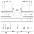
도 4는 본 발명의 일실시예에 따른 곡면 표시 패널을 나타낸 평면도이고, 도 5는 본 발명의 일실시예에 따른 곡면 액정 표시 패널의 한 화소를 나타낸 평면도이다. 도 6은 도 4의 VI-VI 선을 따라 자른 단면도이고, 도 7은 도 4의 VII-VII 선을 따라 자른 단면도이다.FIG. 4 is a plan view of a curved display panel according to an embodiment of the present invention, and FIG. 5 is a plan view of a pixel of a curved liquid crystal display panel according to an embodiment of the present invention. FIG. 6 is a sectional view taken along the line VI-VI of FIG. 4, and FIG. 7 is a sectional view taken along the line VII-VII of FIG.
먼저 도 4를 참고하면, 본 발명의 일실시예에 따른 곡면 액정 표시 패널은 유리 또는 플라스틱 등과 같은 재료로 만들어진 기판(110), 기판(110) 위에 형성되어 있는 지붕층(360)을 포함한다. Referring to FIG. 4, a curved liquid crystal display panel according to an embodiment of the present invention includes a
기판(110)은 복수의 화소 영역(PX)을 포함한다. 복수의 화소 영역(PX)은 복수의 화소 행과 복수의 화소 열을 포함하는 매트릭스 형태로 배치되어 있다. 각 화소 영역(PX)은 제1 부화소 영역(PXa) 및 제2 부화소 영역(PXb)를 포함할 수 있다. 제1 부화소 영역(PXa) 및 제2 부화소 영역(PXb)은 상하로 배치될 수 있다.The
제1 부화소 영역(PXa)과 제2 부화소 영역(PXb) 사이에는 화소 행 방향을 따라서 제1 골짜기(V1)가 위치하고 있고, 복수의 화소 열 사이에는 제2 골짜기(V2)가 위치하고 있다.The first valley V1 is located between the first sub pixel region PXa and the second sub pixel region PXb along the pixel row direction and the second valley V2 is located between the plurality of pixel columns.
지붕층(360)은 화소 행 방향으로 형성되어 있다. 이때, 제1 골짜기(V1)에서는 지붕층(360)이 제거되어 지붕층(360) 아래에 위치하는 구성 요소가 외부로 노출될 수 있도록 주입구(307)가 형성되어 있다.The
각 지붕층(360)은 인접한 제2 골짜기(V2) 사이에서 기판(110)으로부터 떨어져 형성됨으로써, 미세 공간(305)이 형성된다. 또한, 각 지붕층(360)은 제2 골짜기(V2)에서는 기판(110)에 부착되도록 형성됨으로써, 미세 공간(305)의 양 측면을 덮도록 한다.Each
상기에서 설명한 본 발명의 일 실시예에 의한 표시 장치의 구조는 예시에 불과하며, 다양한 변형이 가능하다. 예를 들면, 화소 영역(PX), 제1 골짜기(V1), 및 제2 골짜기(V2)의 배치 형태의 변경이 가능하고, 복수의 지붕층(360)은 제1 골짜기(V1)에서 서로 연결될 수도 있으며, 각 지붕층(360)의 일부는 제2 골짜기(V2)에서 기판(110)으로부터 떨어져 형성됨으로써 인접한 미세 공간(305)이 서로 연결될 수도 있다.The structure of the display device according to an embodiment of the present invention is merely an example, and various modifications are possible. For example, the arrangement of the pixel region PX, the first valley V1, and the second valley V2 can be changed, and the plurality of roof layers 360 are connected to each other in the first valley V1 And a portion of each
이어, 도 5 내지 도 7을 참조하여 본 발명의 일실시예에 따른 곡면 액정 표시 패널의 한 화소에 대하여 설명하면 다음과 같다.Next, one pixel of the curved liquid crystal display panel according to one embodiment of the present invention will be described with reference to FIGS. 5 to 7. FIG.
도 5는 본 발명의 일실시예에 따른 표시 패널의 한 화소를 나타낸 평면도이고, 도 6은 도 4의 VI-VI 선을 따라 자른 단면도이고, 도 7은 도 4의 VII-VII 선을 따라 자른 단면도이다.FIG. 5 is a plan view of a pixel of a display panel according to an embodiment of the present invention, FIG. 6 is a sectional view taken along the line VI-VI of FIG. 4, Sectional view.
도 5 내지 도 7을 참조하면, 기판(110) 위에 복수의 게이트선(121), 복수의 감압 게이트선(123) 및 복수의 유지 전극선(131)을 포함하는 복수의 게이트 도전체가 형성되어 있다.5 to 7, a plurality of gate conductors including a plurality of
게이트선(121) 및 감압 게이트선(123)은 주로 가로 방향으로 뻗어 있으며 게이트 신호를 전달한다. 게이트 도전체는 게이트선(121)으로부터 위아래로 돌출한 제1 게이트 전극(124h) 및 제2 게이트 전극(124l)을 더 포함하고, 감압 게이트선(123)으로부터 위로 돌출한 제3 게이트 전극(124c)을 더 포함한다. 제1 게이트 전극(124h) 및 제2 게이트 전극(124l)은 서로 연결되어 하나의 돌출부를 이룬다. 이때, 제1, 제2, 및 제3 게이트 전극(124h, 124l, 124c)의 돌출 형태는 변경이 가능하다.The
유지 전극선(131)도 주로 가로 방향으로 뻗어 있으며 공통 전압(Vcom) 등의 정해진 전압을 전달한다. 유지 전극선(131)은 위 아래로 돌출한 유지 전극(129), 게이트선(121)과 실질적으로 수직하게 아래로 뻗은 한 쌍의 세로부(134) 및 한 쌍의 세로부(134)의 끝을 서로 연결하는 가로부(127)를 포함한다. 가로부(127)는 아래로 확장된 용량 전극(137)을 포함한다.The sustain
게이트 도전체(121, 123, 124h, 124l, 124c, 131) 위에는 게이트 절연막(gate insulating layer)(140)이 형성되어 있다. 게이트 절연막(140)은 실리콘 질화물(SiNx), 실리콘 산화물(SiOx) 등과 같은 무기 절연 물질로 이루어질 수 있다. 또한, 게이트 절연막(140)은 단일막 또는 다중막으로 이루어질 수 있다.A
게이트 절연막(140) 위에는 제1 반도체(154h), 제2 반도체(154l), 및 제3 반도체(154c)가 형성되어 있다. 제1 반도체(154h)는 제1 게이트 전극(124h) 위에 위치할 수 있고, 제2 반도체(154l)는 제2 게이트 전극(124l) 위에 위치할 수 있으며, 제3 반도체(154c)는 제3 게이트 전극(124c) 위에 위치할 수 있다. 제1 반도체(154h)와 제2 반도체(154l)는 서로 연결될 수 있고, 제2 반도체(154l)와 제3 반도체(154c)도 서로 연결될 수 있다. 또한, 제1 반도체(154h)는 데이터선(171)의 아래까지 연장되어 형성될 수도 있다. 제1 내지 제3 반도체(154h, 154l, 154c)는 비정질 실리콘(amorphous silicon), 다결정 실리콘(polycrystalline silicon), 금속 산화물(metal oxide) 등으로 이루어질 수 있다.A
제1 내지 제3 반도체(154h, 154l, 154c) 위에는 각각 저항성 접촉 부재(ohmic contact)(도시하지 않음)가 더 형성될 수 있다. 저항성 접촉 부재는 실리사이드(silicide) 또는 n형 불순물이 고농도로 도핑되어 있는 n+ 수소화 비정질 규소 따위의 물질로 만들어질 수 있다.Resistive ohmic contacts (not shown) may further be formed on the first to
제1 내지 제3 반도체(154h, 154l, 154c) 위에는 데이터선(data line)(171), 제1 소스 전극(173h), 제2 소스 전극(173l), 제3 소스 전극(173c), 제1 드레인 전극(175h), 제2 드레인 전극(175l), 및 제3 드레인 전극(175c)을 포함하는 데이터 도전체가 형성되어 있다.A
데이터선(171)은 데이터 신호를 전달하며 주로 세로 방향으로 뻗어 게이트선(121) 및 감압 게이트선(123)과 교차한다. 각 데이터선(171)은 제1 게이트 전극(124h) 및 제2 게이트 전극(124l)을 향하여 뻗으며 서로 연결되어 있는 제1 소스 전극(173h) 및 제2 소스 전극(173l)을 포함한다.The
제1 드레인 전극(175h), 제2 드레인 전극(175l) 및 제3 드레인 전극(175c)은 넓은 한 쪽 끝 부분과 막대형인 다른 쪽 끝 부분을 포함한다. 제1 드레인 전극(175h) 및 제2 드레인 전극(175l)의 막대형 끝 부분은 제1 소스 전극(173h) 및 제2 소스 전극(173l)으로 일부 둘러싸여 있다. 제2 드레인 전극(175l)의 넓은 한 쪽 끝 부분은 다시 연장되어 'U'자 형태로 굽은 제3 소스 전극(173c)을 이룬다. 제3 드레인 전극(175c)의 넓은 끝 부분(177c)은 용량 전극(137)과 중첩하여 감압 축전기(Cstd)를 이루며, 막대형 끝 부분은 제3 소스 전극(173c)으로 일부 둘러싸여 있다.The
제1 게이트 전극(124h), 제1 소스 전극(173h), 및 제1 드레인 전극(175h)은 제1 반도체(154h)와 함께 제1 박막 트랜지스터(Qh)를 형성하고, 제2 게이트 전극(124l), 제2 소스 전극(173l), 및 제2 드레인 전극(175l)은 제2 반도체(154l)와 함께 제2 박막 트랜지스터(Ql)를 형성하며, 제3 게이트 전극(124c), 제3 소스 전극(173c), 및 제3 드레인 전극(175c)은 제3 반도체(154c)와 함께 제3 박막 트랜지스터(Qc)를 형성한다.The
제1 반도체(154h), 제2 반도체(154l), 및 제3 반도체(154c)는 서로 연결되어 선형으로 이루어질 수 있으며, 소스 전극(173h, 173l, 173c)과 드레인 전극(175h, 175l, 175c) 사이의 채널 영역을 제외하고는 데이터 도전체(171, 173h, 173l, 173c, 175h, 175l, 175c) 및 그 하부의 저항성 접촉 부재와 실질적으로 동일한 평면 모양을 가질 수 있다.The
제1 반도체(154h)에는 제1 소스 전극(173h)과 제1 드레인 전극(175h) 사이에서 제1 소스 전극(173h) 및 제1 드레인 전극(175h)에 의해 가리지 않고 노출된 부분이 있고, 제2 반도체(154l)에는 제2 소스 전극(173l)과 제2 드레인 전극(175l) 사이에서 제2 소스 전극(173l) 및 제2 드레인 전극(175l)에 의해 가리지 않고 노출된 부분이 있으며, 제3 반도체(154c)에는 제3 소스 전극(173c)과 제3 드레인 전극(175c) 사이에서 제3 소스 전극(173c) 및 제3 드레인 전극(175c)에 의해 가리지 않고 노출된 부분이 있다.The
데이터 도전체(171, 173h, 173l, 173c, 175h, 175l, 175c) 및 각 소스 전극(173h/173l/173c)과 각 드레인 전극(175h/175l/175c) 사이로 노출되어 있는 반도체(154h, 154l, 154c) 위에는 보호막(180)이 형성되어 있다. 보호막(180)은 유기 절연 물질 또는 무기 절연 물질로 이루어질 수 있으며, 단일막 또는 다중막으로 형성될 수 있다.The
보호막(180) 위에는 각 화소 영역(PX) 내에 색필터(230)가 형성되어 있다. 각 색필터(230)는 적색, 녹색 및 청색의 삼원색 등 기본색(primary color) 중 하나를 표시할 수 있다. 색필터(230)는 적색, 녹색, 및 청색의 삼원색에 한정되지 아니하고, 청록색(cyan), 자홍색(magenta), 옐로(yellow), 화이트 계열의 색 등을 표시할 수도 있다. 도시된 바와 달리 색필터(230)는 이웃하는 데이터선(171) 사이를 따라서 열 방향으로 길게 뻗을 수도 있다.A
이웃하는 색필터(230) 사이의 영역에는 차광 부재(220)가 형성되어 있다. 차광 부재(220)는 화소 영역(PX)의 경계부와 박막 트랜지스터 위에 형성되어 빛샘을 방지할 수 있다. 색필터(230)는 각 제1 부화소 영역(PXa)과 제2 부화소 영역(PXb)에 형성되고, 제1 부화소 영역(PXa)과 제2 부화소 영역(PXb) 사이에는 차광 부재(220)가 형성될 수 있다. A
차광 부재(220)는 게이트선(121) 및 감압 게이트선(123)을 따라 뻗어 위아래로 확장되어 있으며 제1 박막 트랜지스터(Qh), 제2 박막 트랜지스터(Ql) 및 제3 박막 트랜지스터(Qc) 등이 위치하는 영역을 덮는 가로 차광 부재(220a)와 데이터선(171)을 따라 뻗어 있는 세로 차광 부재(220b)를 포함한다. 즉, 가로 차광 부재(220a)는 제1 골짜기(V1)에 형성되고, 세로 차광 부재(220b)는 제2 골짜기(V2)에 형성될 수 있다. 색필터(230)와 차광 부재(220)는 일부 영역에서 서로 중첩될 수도 있다.The
색필터(230) 및 차광 부재(220) 위에는 제1 절연층(240)이 더 형성될 수 있다. 제1 절연층(240)은 실리콘 질화물(SiNx), 실리콘 산화물(SiOx), 실리콘 질화산화물(SiOxNy) 등과 같은 무기 절연 물질로 이루어질 수 있다. 제1 절연층(240)은 유기 물질로 이루어진 색필터(230) 및 차광 부재(220)를 보호하는 역할을 하며, 필요에 따라 생략될 수도 있다.The first insulating
제1 절연층(240), 차광 부재(220), 보호막(180)에는 제1 드레인 전극(175h)의 넓은 끝 부분과 제2 드레인 전극(175l)의 넓은 끝 부분을 각각 드러내는 복수의 제1 접촉 구멍(185h) 및 복수의 제2 접촉 구멍(185l)이 형성되어 있다.The first insulating
제1 절연층(240) 위에는 화소 전극(191)이 형성되어 있다. 화소 전극(191)은 인듐-주석 산화물(ITO, Indium Tin Oxide), 인듐-아연 산화물(IZO, Indium Zinc Oxide) 등과 같은 투명한 금속 물질로 이루어질 수 있다.A
화소 전극(191)은 게이트선(121) 및 감압 게이트선(123)을 사이에 두고 서로 분리되어, 게이트선(121) 및 감압 게이트선(123)을 중심으로 화소 영역(PX)의 위와 아래에 배치되어 열 방향으로 이웃하는 제1 부화소 전극(191h)과 제2 부화소 전극(191l)을 포함한다. 즉, 제1 부화소 전극(191h)과 제2 부화소 전극(191l)은 제1 골짜기(V1)를 사이에 두고 분리되어 있으며, 제1 부화소 전극(191h)은 제1 부화소 영역(PXa)에 위치하고, 제2 부화소 전극(191l)은 제2 부화소 영역(PXb)에 위치한다.The
제1 부화소 전극(191h) 및 제2 부화소 전극(191l)은 제1 접촉 구멍(185h) 및 제2 접촉 구멍(185l)을 통하여 각기 제1 드레인 전극(175h) 및 제2 드레인 전극(175l)과 연결되어 있다. 따라서, 제1 박막 트랜지스터(Qh) 및 제2 박막 트랜지스터(Ql)가 온 상태일 때 제1 드레인 전극(175h) 및 제2 드레인 전극(175l)으로부터 데이터 전압을 인가 받는다.The
제1 부화소 전극(191h) 및 제2 부화소 전극(191l) 각각의 전체적인 모양은 사각형이며 제1 부화소 전극(191h) 및 제2 부화소 전극(191l) 각각은 가로 줄기부(193h, 193l), 가로 줄기부(193h, 193l)와 교차하는 세로 줄기부(192h, 192l)로 이루어진 십자형 줄기부를 포함한다. 또한, 제1 부화소 전극(191h) 및 제2 부화소 전극(191l)은 각각 복수의 미세 가지부(194h, 194l), 부화소 전극(191h, 191l)의 가장자리 변에서 아래 또는 위로 돌출된 돌출부(197h, 197l)를 포함한다.The
화소 전극(191)은 가로 줄기부(193h, 193l)와 세로 줄기부(192h, 192l)에 의해 4개의 부영역으로 나뉘어진다. 미세 가지부(194h, 194l)는 가로 줄기부(193h, 193l) 및 세로 줄기부(192h, 192l)로부터 비스듬하게 뻗어 있으며 그 뻗는 방향은 게이트선(121) 또는 가로 줄기부(193h, 193l)와 대략 45도 또는 135도의 각을 이룰 수 있다. 또한 이웃하는 두 부영역의 미세 가지부(194h, 194l)가 뻗어 있는 방향은 서로 직교할 수 있다.The
본 실시예에서 제1 부화소 전극(191h)은 외곽을 둘러싸는 외곽 줄기부를 더 포함하고, 제2 부화소 전극(191l)은 상단 및 하단에 위치하는 가로부 및 제1 부화소 전극(191h)의 좌우에 위치하는 좌우 세로부(198)를 더 포함한다. 좌우 세로부(198)는 데이터선(171)과 제1 부화소 전극(191h) 사이의 용량성 결합, 즉 커플링을 방지할 수 있다.In this embodiment, the
상기에서 설명한 화소 영역의 배치 형태, 박막 트랜지스터의 구조 및 화소 전극의 형상은 하나의 예에 불과하며, 본 발명은 이에 한정되지 아니하고 다양한 변형이 가능하다.The arrangement of the pixel region, the structure of the thin film transistor, and the shape of the pixel electrode described above are only examples, and the present invention is not limited thereto and various modifications are possible.
화소 전극(191) 위에는 화소 전극(191)으로부터 일정한 거리를 가지고 이격되도록 공통 전극(270)이 형성되어 있다. 화소 전극(191)과 공통 전극(270) 사이에는 미세 공간(microcavity, 305)이 형성되어 있다. 즉, 미세 공간(305)은 화소 전극(191) 및 공통 전극(270)에 의해 둘러싸여 있다. 미세 공간(305)의 폭과 넓이는 표시 장치의 크기 및 해상도에 따라 다양하게 변경될 수 있다.A
공통 전극(270)은 인듐-주석 산화물(ITO, Indium Tin Oxide), 인듐-아연 산화물(IZO, Indium Zinc Oxide) 등과 같은 투명한 금속 물질로 이루어질 수 있다. 공통 전극(270)에는 일정한 전압이 인가될 수 있고, 화소 전극(191)과 공통 전극(270) 사이에 전계가 형성될 수 있다.The
화소 전극(191) 위에는 제1 배향막(11)이 형성되어 있다. 제1 배향막(11)은 화소 전극(191)에 의해 덮여있지 않은 제1 절연층(240) 바로 위에도 형성될 수 있다.A
제1 배향막(11)과 마주보도록 공통 전극(270) 아래에는 제2 배향막(21)이 형성되어 있다.A
제1 배향막(11)과 제2 배향막(21)은 수직 배향막으로 이루어질 수 있고, 폴리 아믹산(Polyamic acid), 폴리 실록산(Polysiloxane), 폴리 이미드(Polyimide) 등의 배향 물질로 이루어질 수 있다. 제1 및 제2 배향막(11, 21)은 화소 영역(PX)의 가장자리에서 서로 연결될 수 있다.The
화소 전극(191)과 공통 전극(270) 사이에 위치한 미세 공간(305) 내에는 액정 분자(310)들로 이루어진 액정층이 형성되어 있다. 액정 분자(310)들은 음의 유전율 이방성을 가지며, 전계가 인가되지 않은 상태에서 기판(110)에 수직한 방향으로 서 있을 수 있다. 즉, 수직 배향이 이루어질 수 있다.A liquid crystal layer made of liquid crystal molecules 310 is formed in the
데이터 전압이 인가된 제1 부화소 전극(191h) 및 제2 부화소 전극(191l)은 공통 전극(270)과 함께 전기장을 생성함으로써 두 전극(191, 270) 사이의 미세 공간(305) 내에 위치한 액정 분자(310)의 방향을 결정한다. 이와 같이 결정된 액정 분자(310)의 방향에 따라 액정층을 통과하는 빛의 휘도가 달라진다.The
공통 전극(270) 위에는 제2 절연층(350)이 더 형성될 수 있다. 제2 절연층(350)은 실리콘 질화물(SiNx), 실리콘 산화물(SiOx), 실리콘 질화산화물(SiOxNy) 등과 같은 무기 절연 물질로 이루어질 수 있으며, 필요에 따라 생략될 수도 있다.A second insulating
제2 절연층(350) 위에는 지붕층(360)이 형성되어 있다. 지붕층(360)은 유기 물질로 이루어질 수 있다. 지붕층(360)의 아래에는 미세 공간(305)이 형성되어 있고, 지붕층(360)은 경화 공정에 의해 단단해져 미세 공간(305)의 형상을 유지할 수 있다. 즉, 지붕층(360)은 화소 전극(191)과 미세 공간(305)을 사이에 두고 이격되도록 형성되어 있다.A
지붕층(360)은 화소 행을 따라 각 화소 영역(PX) 및 제2 골짜기(V2)에 형성되며, 제1 골짜기(V1)에는 형성되지 않는다. 즉, 지붕층(360)은 제1 부화소 영역(PXa)과 제2 부화소 영역(PXb) 사이에는 형성되지 않는다. 각 제1 부화소 영역(PXa)과 제2 부화소 영역(PXb)에서는 각 지붕층(360)의 아래에 미세 공간(305)이 형성되어 있다. 제2 골짜기(V2)에서는 지붕층(360)의 아래에 미세 공간(305)이 형성되지 않으며, 기판(110)에 부착되도록 형성되어 있다. 따라서, 제2 골짜기(V2)에 위치하는 지붕층(360)의 두께가 각 제1 부화소 영역(PXa) 및 제2 부화소 영역(PXb)에 위치하는 지붕층(360)의 두께보다 두껍게 형성될 수 있다. 미세 공간(305)의 상부면 및 양측면은 지붕층(360)에 의해 덮여 있는 형태로 이루어지게 된다.The
또한, 지붕층(360)은 곡면 액정 표시 패널에서 다양한 곡률을 가질 수 있도록 형성하기 위해 다양한 두께로 형성될 수 있다. In addition, the
공통 전극(270), 제2 절연층(350), 및 지붕층(360)에는 미세 공간(305)의 일부를 노출시키는 주입구(307)가 형성되어 있다. 주입구(307)는 제1 부화소 영역(PXa)과 제2 부화소 영역(PXb)의 가장자리에 서로 마주보도록 형성될 수 있다. 즉, 주입구(307)는 제1 부화소 영역(PXa)의 하측 변, 제2 부화소 영역(PXb)의 상측 변에 대응하여 미세 공간(305)의 측면을 노출시키도록 형성될 수 있다. 주입구(307)에 의해 미세 공간(305)이 노출되어 있으므로, 주입구(307)를 통해 미세 공간(305) 내부로 배향액 또는 액정 물질 등을 주입할 수 있다.The
제3 절연층(370) 위에는 덮개막(390)이 형성될 수 있다. 덮개막(390)은 미세 공간(305)의 일부를 외부로 노출시키는 주입구(307)를 덮도록 형성된다. 즉, 덮개막(390)은 미세 공간(305)의 내부에 형성되어 있는 액정 분자(310)가 외부로 나오지 않도록 미세 공간(305)을 밀봉할 수 있다. 덮개막(390)은 액정 분자(310)과 접촉하게 되므로, 액정 분자(310)과 반응하지 않는 물질로 이루어지는 것이 바람직하다. 예를 들면, 덮개막(390)은 페릴렌(Parylene) 등으로 이루어질 수 있다.A
덮개막(390)은 이중막, 삼중막 등과 같이 다중막으로 이루어질 수도 있다. 이중막은 서로 다른 물질로 이루어진 두 개의 층으로 이루어져 있다. 삼중막은 세 개의 층으로 이루어지고, 서로 인접하는 층의 물질이 서로 다르다. 예를 들면, 덮개막(390)은 유기 절연 물질로 이루어진 층과 무기 절연 물질로 이루어진 층을 포함할 수 있다.The
이렇게 형성된 액정 표시 장치의 상하부 면에는 편광판(12, 22)이 더 형성되어 있다. 편광판(12, 22)은 제1 편광판(12) 및 제2 편광판(22)으로 이루어질 수 있다. Polarizing
제1 편광판(12)은 액정 표시 패널의 단축(A-A) 방향의 편광축을 가지고 있으며, 제2 편광판(22)은 제1 편광판(12)의 편광축에 직각을 이루는 방향인 액정 표시 패널의 장축(B-B) 방향의 편광축을 가지고 있다.The first
제1 편광판(12)은 기판(110)의 상부로서, 덮개막(390) 상부면에 부착되고, 제2 편광판(22)은 기판(110)의 하부면 위에 부착될 수 있다.The first
제1 편광판(12)은 고온에서 변형 될 수 있는 접착제로 이루어진 제1 접착제층(13)에 의해 접착되어 있을 수 있고, 제2 편광판(22)은 고온에서 변형이 일어나지 않는 고온 변형율 개선 접착제로 이루어진 제2 접착체층(23)에 의해 접착되어 있을 수 있다.The first
다음으로, 도 8 내지 도 14를 참고하여 본 발명의 일실시예에 따른 곡면 액정 표시 장치의 제조 방법에 대해서 상세하게 설명한다.Next, a method of manufacturing a curved LCD according to an embodiment of the present invention will be described in detail with reference to FIGS. 8 to 14. FIG.
도 8 내지 도 14는 본 발명의 일실시예에 따른 곡면 액정 표시 장치의 제조 방법을 순서대로 나타낸 도면이다.8 to 14 are views sequentially illustrating a method of manufacturing a curved liquid crystal display device according to an embodiment of the present invention.
먼저, 도 8에 도시된 바와 같이, 유리 또는 플라스틱 등으로 이루어진 기판(110) 위에 일방향으로 뻗어있는 게이트선(121)과 감압 게이트선(123)을 형성하고, 게이트선(121)으로부터 돌출되는 제1 게이트 전극(124h), 제2 게이트 전극(124l), 및 제3 게이트 전극(124c)을 형성한다.8, a
또한, 게이트선(121), 감압 게이트선(123), 및 제1 내지 제3 게이트 전극(124h, 124l, 124c)와 이격되도록 유지 전극선(131)을 함께 형성할 수 있다.The
이어, 게이트선(121), 감압 게이트선(123), 제1 내지 제3 게이트 전극(124h, 124l, 124c), 및 유지 전극선(131)을 포함한 기판(110) 위의 전면에 실리콘 산화물(SiOx) 또는 실리콘 질화물(SiNx)과 같은 무기 절연 물질을 이용하여 게이트 절연막(140)을 형성한다. 게이트 절연막(140)은 단일막 또는 다중막으로 형성할 수 있다.Next, silicon oxide (SiOx) is deposited on the entire surface of the
이어, 게이트 절연막(140) 위에 비정질 실리콘(amorphous silicon), 다결정 실리콘(polycrystalline silicon), 금속 산화물(metal oxide) 등과 같은 반도체 물질을 증착한 후 이를 패터닝하여 제1 반도체(154h), 제2 반도체(154l), 및 제3 반도체(154c)를 형성한다. 제1 반도체(154h)는 제1 게이트 전극(124h) 위에 위치하도록 형성하고, 제2 반도체(154l)는 제2 게이트 전극(124l) 위에 위치하도록 형성하며, 제3 반도체(154c)는 제3 게이트 전극(124c) 위에 위치하도록 형성할 수 있다.Next, a semiconductor material such as amorphous silicon, polycrystalline silicon, metal oxide, or the like is deposited on the
이어, 금속 물질을 증착한 후 이를 패터닝하여 타방향으로 뻗어있는 데이터선(171)을 형성한다. 금속 물질은 단일막 또는 다중막으로 이루어질 수 있다.Then, a metal material is deposited and patterned to form a
또한, 데이터선(171)으로부터 제1 게이트 전극(124h) 위로 돌출되는 제1 소스 전극(173h) 및 제1 소스 전극(173h)과 이격되는 제1 드레인 전극(175h)을 함께 형성한다. 또한, 제1 소스 전극(173h)과 연결되어 있는 제2 소스 전극(173l) 및 제2 소스 전극(173l)과 이격되는 제2 드레인 전극(175l)을 함께 형성한다. 또한, 제2 드레인 전극(175l)으로부터 연장되어 있는 제3 소스 전극(173c) 및 제3 소스 전극(173c)과 이격되는 제3 드레인 전극(175c)을 함께 형성한다.A
반도체 물질과 금속 물질을 연속으로 증착한 후 이를 동시에 패터닝하여 제1 내지 제3 반도체(154h, 154l, 154c), 데이터선(171), 제1 내지 제3 소스 전극(173h, 173l, 173c), 및 제1 내지 제3 드레인 전극(175h, 175l, 175c)을 형성할 수도 있다. 이때, 제1 반도체(154h)는 데이터선(171)의 아래까지 연장되어 형성된다.The first to
제1/제2/제3 게이트 전극(124h/124l/124c), 제1/제2/제3 소스 전극(173h/173l/173c), 및 제1/제2/제3 드레인 전극(175h/175l/175c)은 제1/제2/제3 반도체(154h/154l/154c)와 함께 각각 제1/제2/제3 박막 트랜지스터(thin film transistor, TFT)(Qh/Ql/Qc)를 구성한다.Second and
이어, 데이터선(171), 제1 내지 제3 소스 전극(173h, 173l, 173c), 제1 내지 제3 드레인 전극(175h, 175l, 175c), 및 각 소스 전극(173h/173l/173c)과 각 드레인 전극(175h/175l/175c) 사이로 노출되어 있는 반도체(154h, 154l, 154c) 위에 보호막(180)을 형성한다. 보호막(180)은 유기 절연 물질 또는 무기 절연 물질로 이루어질 수 있으며, 단일막 또는 다중막으로 형성될 수 있다.Next, the
이어, 보호막(180) 위의 각 화소 영역(PX) 내에 색필터(230)를 형성한다. 색필터(230)는 각 제1 부화소 영역(PXa)과 제2 부화소 영역(PXb)에 형성하고, 제1 골짜기(V1)에는 형성하지 않을 수 있다. 또한, 복수의 화소 영역(PX)의 열 방향을 따라 동일한 색의 색필터(230)를 형성할 수 있다. 세 가지 색의 색필터(230)를 형성하는 경우 제1 색의 색필터(230)를 먼저 형성한 후 마스크를 쉬프트 시켜 제2 색의 색필터(230)를 형성할 수 있다. 이어, 제2 색의 색필터(230)를 형성한 후 마스크를 쉬프트시켜 제3 색의 색필터를 형성할 수 있다.Next, a
이어, 보호막(180) 위의 각 화소 영역(PX)의 경계부 및 박막 트랜지스터 위에 차광 부재(220)를 형성한다. 제1 부화소 영역(PXa)과 제2 부화소 영역(PXb)의 사이에 위치하는 제1 골짜기(V1)에도 차광 부재(220)를 형성할 수 있다.Next, the
상기에서 색필터(230)를 형성한 후 차광 부재(220)를 형성하는 것으로 설명하였으나, 본 발명은 이에 한정되지 아니하고 차광 부재(220)를 먼저 형성한 후 색필터(230)를 형성할 수도 있다.The
이어, 색필터(230) 및 차광 부재(220) 위에 실리콘 질화물(SiNx), 실리콘 산화물(SiOx), 실리콘 질화산화물(SiOxNy) 등과 같은 무기 절연 물질로 제1 절연층(240)을 형성한다.The first insulating
이어, 보호막(180), 차광 부재(220), 및 제1 절연층(240)을 식각하여 제1 드레인 전극(175h)의 일부가 노출되도록 제1 접촉 구멍(185h)을 형성하고, 제2 드레인 전극(175l)의 일부가 노출되도록 제2 접촉 구멍(185l)을 형성한다.The
이어, 제1 절연층(240) 위에 인듐-주석 산화물(ITO, Indium Tin Oxide), 인듐-아연 산화물(IZO, Indium Zinc Oxide) 등과 같은 투명한 금속 물질을 증착한 후 패터닝하여 제1 부화소 영역(PXa) 내에 제1 부화소 전극(191h)을 형성하고, 제2 부화소 영역(PXb) 내에 제2 부화소 전극(191l)을 형성한다. 제1 부화소 전극(191h)과 제2 부화소 전극(191l)은 제1 골짜기(V1)를 사이에 두고 분리되어 있다. 제1 부화소 전극(191h)은 제1 접촉 구멍(185h)을 통해 제1 드레인 전극(175h)과 연결되도록 형성하고, 제2 부화소 전극(191l)은 제2 접촉 구멍(185l)을 통해 제2 드레인 전극(175l)과 연결되도록 형성한다.A transparent metal material such as indium tin oxide (ITO), indium zinc oxide (IZO), or the like is deposited on the first insulating
제1 부화소 전극(191h) 및 제2 부화소 전극(191l) 각각에 가로 줄기부(193h, 193l), 가로 줄기부(193h, 193l)와 교차하는 세로 줄기부(192h, 192l)를 형성한다. 또한, 가로 줄기부(193h, 193l) 및 세로 줄기부(192h, 192l)로부터 비스듬하게 뻗어있는 복수의 미세 가지부(194h, 194l)를 형성한다.The vertical
도 9에 도시된 바와 같이, 화소 전극(191) 위에 감광성 유기 물질을 도포하고, 포토 공정을 통해 희생층(300)을 형성한다.9, a photosensitive organic material is applied on the
희생층(300)은 복수의 화소 열을 따라 연결되도록 형성된다. 즉, 희생층(300)은 각 화소 영역(PX)을 덮도록 형성되고, 제1 부화소 영역(PXa)과 제2 부화소 영역(PXb) 사이에 위치한 제1 골짜기(V1)를 덮도록 형성된다.The
이어, 희생층(300) 위에 인듐-주석 산화물(ITO, Indium Tin Oxide), 인듐-아연 산화물(IZO, Indium Zinc Oxide) 등과 같은 투명한 금속 물질을 증착하여 공통 전극(270)을 형성한다.A transparent electrode material such as indium tin oxide (ITO), indium zinc oxide (IZO), or the like is deposited on the
이어, 공통 전극(270) 위에 실리콘 질화물(SiNx), 실리콘 산화물(SiOx), 실리콘 질화산화물(SiOxNy) 등과 같은 무기 절연 물질로 제2 절연층(350)을 형성할 수 있다.The second
이어, 제2 절연층(350) 위에 유기 물질을 도포하고, 패터닝하여 지붕층(360)을 형성한다. 이때, 제1 골짜기(V1)에 위치한 유기 물질이 제거되도록 패터닝할 수 있다. 이에 따라 지붕층(360)은 복수의 화소 행을 따라 연결되는 형태로 이루어지게 된다.Then, an organic material is applied on the second insulating
지붕층(360)은 추후 곡면 액정 표시 패널을 제조하기 위해 고온으로 처리 시 다양한 곡률로 형성 가능하도록 두께를 다양하게 형성할 수 있다.The thickness of the
다음 도 10에 도시된 바와 같이, 지붕층(360)을 마스크로 이용하여 제2 절연층(350) 및 공통 전극(270)을 패터닝한다. 먼저, 지붕층(360)을 마스크로 이용하여 제2 절연층(350)을 건식 식각한 후 공통 전극(270)을 습식 식각한다.10, the second insulating
다음으로 도 11에 도시된 바와 같이, 지붕층(360) 위에 실리콘 질화물(SiNx), 실리콘 산화물(SiOx), 실리콘 질화산화물(SiOxNy) 등과 같은 무기 절연 물질로 제3 절연층(370)을 형성할 수 있다.Next, as shown in FIG. 11, a third
이어, 제3 절연층(370) 위에 포토 레지스트(500)를 도포하고, 포토 공정을 통해 포토 레지스트(500)를 패터닝한다. 이때, 제1 골짜기(V1)에 위치한 포토 레지스트(500)를 제거할 수 있다. 패터닝된 포토 레지스트(500)를 마스크로 이용하여 제3 절연층(370)을 식각한다. 즉, 제1 골짜기(V1)에 위치한 제3 절연층(370)을 제거한다.Next, a
제3 절연층(370)은 지붕층(360)의 상부면 및 측면을 덮도록 형성하여 지붕층(360)을 보호하는 역할을 수행하도록 한다. 제3 절연층(370)의 패턴은 지붕층(360)의 패턴보다 더 바깥쪽에 위치할 수 있다.The third
제2 절연층(350)의 패턴은 제3 절연층(370)의 패턴과 동일하게 이루어질 수 있다. 이와 달리 제2 절연층(350)의 패턴이 지붕층(360)의 패턴보다 안쪽에 위치하도록 형성할 수도 있다. 이때, 제3 절연층(370)이 제2 절연층(350)과 접촉하도록 형성하는 것이 바람직하다.The pattern of the second insulating
상기에서 지붕층(360)을 패터닝하는 설비와 제3 절연층(370)을 패터닝하는 설비는 상이할 수 있으며, 이들 설비 간의 정렬 오류로 인해 제3 절연층(370)과 지붕층(360)의 패턴의 차이가 커질 수 있다. 이때, 제3 절연층(370)의 패턴이 지붕층(360)의 패턴보다 바깥쪽에 위치하는 부분이 처지거나 부러질 수 있으나, 제3 절연층(370)은 도전성 부재가 아니므로 화소 전극(191)과의 단락 등의 문제가 발생하지 않는다.The apparatus for patterning the
상기에서 제3 절연층(370)을 형성하는 공정에 대해 설명하였으나, 본 발명은 이에 한정되지 아니하고, 제3 절연층(370)을 형성하지 않을 수도 있다. 제3 절연층(370)을 형성하지 않을 경우 지붕층(360)을 패터닝하는 설비와 제3 절연층(370)을 패터닝하는 설비 간의 정렬 오류에 의해 발생하는 문제점을 방지할 수 있다.Although the process of forming the third insulating
또한, 제2 절연층(350) 및 공통 전극(270)은 지붕층(360)을 마스크로 이용하여 패터닝하게 되므로 정렬 오류가 발생하지 않게 된다. In addition, since the second insulating
도 12에 도시된 바와 같이, 희생층(300)이 노출된 기판(110) 위에 현상액 또는 스트리퍼 용액 등을 공급하여 희생층(300)을 전면 제거하거나, 애싱(ashing) 공정을 이용하여 희생층(300)을 전면 제거한다.12, the
희생층(300)이 제거되면, 희생층(300)이 위치하였던 자리에 미세 공간(305)이 생긴다.When the
화소 전극(191)과 공통 전극(270)은 미세 공간(305)을 사이에 두고 서로 이격되고, 화소 전극(191)과 지붕층(360)은 미세 공간(305)을 사이에 두고 서로 이격된다. 공통 전극(270)과 지붕층(360)은 미세 공간(305)의 상부면과 양측면을 덮도록 형성된다.The
지붕층(360), 제2 절연층(350), 및 공통 전극(270)이 제거된 부분을 통해 미세 공간(305)은 외부로 노출되어 있으며, 이를 주입구(307)라 한다. 주입구(307)는 제1 골짜기(V1)를 따라 형성되어 있다. 예를 들면, 주입구(307)는 제1 부화소 영역(PXa)과 제2 부화소 영역(PXb)의 가장자리에 서로 마주보도록 형성될 수 있다. 즉, 주입구(307)는 제1 부화소 영역(PXa)의 하측 변, 제2 부화소 영역(PXb)의 상측 변에 대응하여 미세 공간(305)의 측면을 노출시키도록 형성될 수 있다. 이와 상이하게, 주입구(307)가 제2 골짜기(V2)를 따라 형성되도록 할 수도 있다.The
이어, 기판(110)에 열을 가하여 지붕층(360)을 경화시킨다. 지붕층(360)에 의해 미세 공간(305)의 형상이 유지되도록 하기 위함이다. Heat is then applied to the
이어, 스핀 코팅 방식 또는 잉크젯 방식으로 배향 물질이 포함되어 있는 배향액을 기판(110) 위에 떨어뜨리면, 배향액이 주입구(307)를 통해 미세 공간(305) 내부로 주입된다. 배향액을 미세 공간(305)의 내부로 주입한 후 경화 공정을 진행하면 용액 성분은 증발하고, 배향 물질이 미세 공간(305) 내부의 벽면에 남게 된다.Then, when the alignment liquid containing the alignment material is dropped on the
따라서, 화소 전극(191) 위에 제1 배향막(11)을 형성하고, 공통 전극(270) 아래에 제2 배향막(21)을 형성할 수 있다. 제1 배향막(11)과 제2 배향막(21)은 미세 공간(305)을 사이에 두고 마주보도록 형성되고, 화소 영역(PX)의 가장자리에서는 서로 연결되도록 형성된다.Accordingly, the
이때, 제1 및 제2 배향막(11, 21)은 미세 공간(305)의 측면을 제외하고는 기판(110)에 대해 수직한 방향으로 배향이 이루어질 수 있다. 추가로 제1 및 제2 배향막(11, 21)에 UV를 조사하는 공정을 진행함으로써, 기판(110)에 대해 수평한 방향으로 배향이 이루어지도록 할 수도 있다.At this time, the first and second alignment layers 11 and 21 may be oriented in a direction perpendicular to the
이어, 잉크젯 방식 또는 디스펜싱 방식으로 액정 분자(310)들로 이루어진 액정 물질을 기판(110) 위에 떨어뜨리면, 액정 물질이 주입구(307)를 통해 미세 공간(305) 내부로 주입된다. 이때, 액정 물질을 홀수 번째 제1 골짜기(V1)를 따라 형성된 주입구(307)에는 떨어뜨리고, 짝수 번째 제1 골짜기(V1)를 따라 형성된 주입구(307)에는 떨어뜨리지 않을 수 있다. 이와 반대로, 액정 물질을 짝수 번째 제1 골짜기(V1)를 따라 형성된 주입구(307)에 떨어뜨리고, 홀수 번째 제1 골짜기(V1)를 따라 형성된 주입구(307)에는 떨어뜨리지 않을 수 있다.When the liquid crystal material composed of the liquid crystal molecules 310 is dropped on the
홀수 번째 제1 골짜기(V1)를 따라 형성된 주입구(307)에 액정 물질을 떨어뜨리면 모세관력(capillary force)에 의해 액정 물질이 주입구(307)를 통과하여 미세 공간(305) 내부로 들어가게 된다. 이때, 짝수 번째 제1 골짜기(V1)를 따라 형성된 주입구(307)를 통해 미세 공간(305) 내부의 공기가 빠져나감으로써, 액정 물질이 미세 공간(305) 내부로 들어가게 된다.When the liquid crystal material is dropped on the
또한, 액정 물질을 모든 주입구(307)에 떨어뜨릴 수도 있다. 즉, 액정 물질을 홀수 번째 제1 골짜기(V1)를 따라 형성된 주입구(307)와 짝수 번째 제1 골짜기(V1)를 따라 형성된 주입구(307)에 모두 떨어뜨릴 수도 있다.In addition, the liquid crystal material may be dropped to all of the
도 13에 도시된 바와 같이, 제3 절연층(370) 위에 액정 분자(310)와 반응하지 않는 물질을 증착하여 덮개막(390)을 형성한다. 덮개막(390)은 미세 공간(305)이 외부로 노출되어 있는 주입구(307)를 덮도록 형성되어 미세 공간(305)을 밀봉한다.13, a material that does not react with the liquid crystal molecules 310 is deposited on the third insulating
이어, 도 14에 도시한 바와 같이, 액정 표시 패널의 상하부 면에 제1 편광판(12) 및 제2 편광판(22)을 각각 접착제를 이용하여 부착한다.Next, as shown in Fig. 14, the first
제1 편광판(12)은 액정 표시 패널의 단축(A-A) 방향의 편광축을 가지고 있으며, 제2 편광판(22)은 제1 편광판(12)의 편광축에 직각을 이루는 방향인 액정 표시 패널의 장축(B-B) 방향의 편광축을 가지도록 형성한다.The first
제1 편광판(12)은 덮개막(390)의 위에 상부면에 부착되고, 제2 편광판(22)은 기판(110)의 하부면 위에 부착할 수 있다.The first
제1 편광판(12)은 고온에서 변형될 수 있는 접착제로 이루어진 제1 접착제층(13)에 의해 접착할 수 있고, 제2 편광판(22)은 고온에서 변형이 일어나지 않는 고온 변형율 개선 접착제로 이루어진 제2 접착제층(23)에 의해 접착할 수 있다.The first
이 후, 완성된 액정 표시 패널(100)을 고온, 고습의 조건에서 열처리하여 곡면으로 형성하는 단계를 거쳐 액정 표시 패널(100)의 단축(A-A) 및 장축(B-B) 양 방향으로 곡률을 가지는 곡면으로 형성한다. Thereafter, the finished liquid
액정 표시 패널(100)을 곡면으로 형성하기 위한 열처리는 형성하고자 하는 곡면의 곡률에 따라서 달라질 수 있으나, 50~70℃에서 50~300시간동안 수행할 수 있으며 열처리 조건은 이에 한정되지 않는다.The heat treatment for forming the curved surface of the liquid
이러한 열처리를 거쳐 본 발명의 일실시예에 따른 곡면 액정 표시 장치를 완성한다.Through this heat treatment, a curved liquid crystal display according to an embodiment of the present invention is completed.
EM 구조를 가지는 액정 표시 패널(100)이 고온, 고습 조건에서 액정 표시 패널(100)의 장축(B-B) 방향에서 곡면으로 꺾이는 것을 확인하기 위해서 EM 구조를 가지는 액정 표시 패널(100) 상부면 또는 하부면에 액정 표시 패널(100)의 장축(B-B) 방향의 편광축을 가지는 제2 편광판(22)을 부착하여 고온, 고습의 열처리를 수행하였다. 이에 대한 비교예로서 EM 구조를 가지는 액정 표시 패널(100) 상부면 또는 하부면에 액정 표시 패널(100)의 단축(A-A) 방향의 편광축을 가지는 제1 편광판(12)을 부착하여 고온, 고습의 열처리를 수행하였다. 이의 결과는 도 15에 나타내었으며, 도 15의 (a)는 비교예에 따른 액정 표시 패널(100)의 곡면 형성 결과를, 도 15의 (b)는 일실시예에 따른 액정 표시 패널(100)의 곡면 형성 결과를 나타내었다.In order to confirm that the liquid
도 15에 나타난 바와 같이, 액정 표시 패널(100)의 단축(A-A) 방향의 편광축을 가진 제1 편광판(12)을 부착한 경우 액정 표시 패널(100)은 제1 편광판(12)을 상부면에 부착한 경우 및 하부면에 부착한 경우 모두 6mm 정도가 휘어 액정 표시 패널(100)의 단축(A-A) 방향에서는 제1 편광판(12)에 의한 곡면의 형성 외에 다른 영향에 의한 곡면의 형성은 존재하지 않는 것을 확인하였다.15, when the first
다만, 액정 표시 패널(100)의 장축(B-B) 방향의 편광축을 가진 제2 편광판(22)을 액정 표시 패널(100)의 상부면에 부착한 경우 액정 표시 패널(100)은 16mm 정도가 휘었으나, 제2 편광판(22)을 액정 표시 패널(100)의 하부면에 부착한 경우 액정 표시 패널(100)은 11mm 정도가 휘어 제2 편광판(22)에 의한 곡면의 형성 외에 다른 힘이 작용하고 있는 것을 확인할 수 있었다.However, when the second
따라서, EM 구조를 가지는 액정 표시 패널(100)은 유기 물질로 형성된 지붕층에 의한 인장 응력(tensile stress)이 액정 표시 패널(100)의 장축(B-B) 방향으로 존재하는 것을 확인할 수 있었다.Therefore, it can be seen that the liquid
액정 표시 패널의 두께에 따른 액정 표시 패널이 휘는 정도를 측정하기 위해서 액정 표시 패널의 두께가 각각 0.5mm, 0.7mm일 때로서, 제1 편광판만을 부착한 경우, 제2 편광판만을 부착한 경우, 제1 편광판 및 제2 편광판을 모두 부착한 경우에 액정 표시 패널이 휘는 정도를 측정하였다. 이의 결과는 도 16에 나타내었다.In order to measure the degree of bending of the liquid crystal display panel according to the thickness of the liquid crystal display panel, the thickness of the liquid crystal display panel was 0.5 mm and 0.7 mm, respectively. In the case of attaching only the first polarizer, The degree of bending of the liquid crystal display panel was measured when both the first polarizing plate and the second polarizing plate were attached. The results are shown in Fig.
도 16에 나타난 바와 같이, 0.5mm 액정 표시 패널의 경우 제1 편광판만을 부착한 경우 5mm, 제2 편광판만을 부착한 경우 14mm, 제1 편광판 및 제2 편광판을 모두 부착한 경우 2mm가 휘어 0.7mm의 액정 표시 패널보다 모든 경우에 더 많이 휘는 것을 확인할 수 있었다. 따라서, 액정 표시 패널의 두께가 얇게 형성될수록 더 큰 곡률을 가진 곡면 액정 표시 장치를 제조할 수 있는 것을 확인할 수 있었다. 16, in the case of a 0.5 mm liquid crystal display panel, 5 mm when only the first polarizing plate was attached, 14 mm when only the second polarizing plate was attached, 2 mm when the first polarizing plate and the second polarizing plate were both bent and 0.7 mm It was confirmed that the liquid crystal display panel was warped more in all cases than the liquid crystal display panel. Accordingly, it has been confirmed that a curved liquid crystal display device having a larger curvature can be manufactured as the thickness of the liquid crystal display panel is reduced.
다음으로, 액정 표시 패널의 크기에 따른 액정 표시 패널의 휘는 정도를 파악하기 위해 10.1인치 액정 표시 패널과 15인치 액정 표시 패널에 패널의 장축 방향의 편광축을 가지는 제2 편광판을 부착하여 휘는 정도를 측정하였다. 이의 결과는 도 17에 나타내었다.Next, in order to grasp the degree of bending of the liquid crystal display panel according to the size of the liquid crystal display panel, the degree of bending of the second polarizer having the polarization axis in the long axis direction of the panel was measured on the 10.1 inch liquid crystal display panel and the 15 inch liquid crystal display panel Respectively. The results are shown in Fig.
도 17에 나타난 바와 같이, 액정 표시 패널이 커짐에 따라 휘는 정도는 대체적으로 선형관계를 나타내고 있어 액정 표시 패널의 크기와 액정 표시 패널이 편광판에 의해 휘는 정도는 일정한 것을 확인할 수 있었다.As shown in FIG. 17, as the size of the liquid crystal display panel increases, the degree of warpage has a generally linear relationship, and it is confirmed that the size of the liquid crystal display panel and the degree of warping of the liquid crystal display panel by the polarizing plate are constant.
지붕층이 형성된 EM 구조를 갖는 액정 표시 패널과 일반적인 기판의 휘는 정도를 비교하기 위해, 동일한 두께를 가지는 지붕층이 형성된 EM 구조를 갖는 액정 표시 패널과 기판에 편광판을 부착하여 휘는 정도를 측정하였다. 이의 결과는 도 18에 나타내었다.In order to compare the degree of bending between a liquid crystal display panel having an EM structure having a roof layer and a general substrate, the polarizing plate was attached to a liquid crystal display panel having an EM structure with a roof layer having the same thickness and the degree of bending was measured. The results are shown in Fig.
도 18에 나타난 바와 같이, 기판에 편광판을 부착한 경우는 2.5mm 정도 휘었으나, 지붕층이 형성된 EM 구조를 갖는 액정 표시 패널에 편광판을 부착한 경우에는 3.5mm 정도가 휘어 액정 표시 패널이 휘는 정도가 1.4배 정도 증가된 것을 확인할 수 있었다.As shown in FIG. 18, when a polarizing plate is attached to a substrate, it is warped by about 2.5 mm. However, when a polarizing plate is attached to a liquid crystal display panel having an EM structure having a roof layer formed, Was increased by 1.4 times.
액정 표시 패널에 편광판을 부착하기 위한 접착제의 종류에 따라 액정 표시 패널이 휘는 정도를 파악하기 위하여, 15인치 패널과 10.1인치 패널 각각에 고온 변형성이 있는 접착제와 고온에서의 변형성이 없는 고온 변형율 개선 접착제를 각각 사용하여 편광판을 부착한 다음 액정 표시 패널이 휘는 정도를 측정하였다. 이의 결과는 도 19에 나타내었다.In order to determine the degree of bending of the liquid crystal display panel depending on the kind of adhesive for attaching the polarizing plate to the liquid crystal display panel, an adhesive having a high temperature deformability and a high temperature strain improving adhesive To measure the degree of bending of the liquid crystal display panel. The results are shown in Fig.
도 19에 나타난 바와 같이, 15인치 액정 표시 패널의 경우 고온 변형율 개선 접착제를 사용하지 않은 경우에 비해 고온 변형율 개선 접착제를 사용한 경우, 액정 표시 패널이 휘는 정도가 3.5mm에서 2.5mm 정도로 감소하였으며, 10.1인치 액정 표시 패널의 경우 고온 변형율 개선 접착제를 사용한 경우 액정 표시 패널이 전혀 휘어지지 않아서 접착제의 종류에 따라서 액정 표시 패널이 휘는 정도가 상이할 수 있음을 확인하였다.As shown in FIG. 19, in the case of a 15-inch liquid crystal display panel, the degree of bending of the liquid crystal display panel was reduced from 3.5 mm to 2.5 mm when a high temperature strain improving adhesive was used, compared with the case where a high temperature strain improving adhesive was not used. Inch liquid crystal display panel, it was confirmed that the degree of warping of the liquid crystal display panel may be different depending on the kind of adhesive because the liquid crystal display panel was not warped at all when the high temperature strain improving adhesive was used.
따라서, 본 발명의 일실시예에 따른 반구형으로 오목한 곡면을 가진 액정 표시 장치를 제조할 시에 액정 표시 패널의 상부면에 부착되는 제1 편광판의 경우는 액정 표시 패널을 곡면으로 형성시키기 위해서 고온에서의 변형성이 있는 접착제를 사용할 수 있음을 확인할 수 있었다. 또한, 액정 표시 패널의 하부면에 부착되는 제2 편광판의 경우는 열처리로 인해 수축될 경우 액정 표시 패널이 볼록한 방향으로 휘어지기 때문에 열처리에 의해 수축되는 것을 방지하기 위해 고온 변형율 개선 접착제를 사용하여야 하는 것을 확인할 수 있었다.Therefore, in the case of manufacturing a liquid crystal display device having a hemispherically concave curved surface according to an embodiment of the present invention, in order to form a liquid crystal display panel as a curved surface, a first polarizer attached to the upper surface of the liquid crystal display panel It is possible to use an adhesive having a deformability of < RTI ID = 0.0 > In the case of the second polarizing plate attached to the lower surface of the liquid crystal display panel, since the liquid crystal display panel is bent in a convex direction when it is shrunk due to the heat treatment, a high temperature strain improving adhesive should be used to prevent shrinkage due to heat treatment .
본 발명의 일실시예에 따른 곡면 액정 표시 장치의 휘도값을 측정하기 위해, 비교예로서 액정 표시 패널의 장축 방향으로만 곡면을 형성한 곡면 액정 표시 장치와, 본 발명의 일실시예에 따른 액정 표시 패널의 장축 및 단축 양 방향으로 곡면을 형성한 곡면 액정 표시 장치의 휘도값을 측정하였다. 이의 결과는 도 20에 나타내었으며, 도 20의 (a)에 비교예의 실험 결과를, 도 20의 (b)에 일실시예의 실험 결과를 나타내었다.In order to measure the luminance value of the curved liquid crystal display device according to an embodiment of the present invention, a curved surface liquid crystal display device in which a curved surface is formed only in the major axis direction of the liquid crystal display panel as a comparative example, The luminance value of a curved surface liquid crystal display device having a curved surface in both major and minor axis directions of the display panel was measured. The results are shown in FIG. 20, FIG. 20 (a) shows the experimental results of the comparative example, and FIG. 20 (b) shows the experimental results of one embodiment.
도 20에 나타난 바와 같이, 본 발명의 일실시예에 따른 곡면 액정 표시 장치가 액정 표시 패널의 일축 방향으로만 곡면을 형성한 곡면 액정 표시 장치와 비교해 휘도값이 상승한 것을 확인할 수 있었다.As shown in FIG. 20, it can be seen that the brightness value of the curved liquid crystal display device according to an embodiment of the present invention is higher than that of the curved surface liquid crystal display device in which the curved surface is formed only in the uniaxial direction of the liquid crystal display panel.
본 발명의 일실시예에 따른 곡면 액정 표시 장치 및 이의 제조 방법에 의해 제조된 곡면 액정 표시 장치는 도 21에 나타난 바와 같이, 시청자가 화면의 중앙부를 보는 경우와 화면의 좌우 양단을 보는 경우의 거리를 유사 또는 동일하게 제작함으로서, 시각차를 감소시켜 임장감을 증대시킬 수 있다.As shown in FIG. 21, the curved liquid crystal display device manufactured by the curved surface liquid crystal display device according to an embodiment of the present invention has a curved surface liquid crystal display device It is possible to reduce the visual difference and increase the sense of durability.
이상과 같은 본 발명의 실시예에 따르면, 액정 표시 패널의 장축 뿐만 아니라 단축을 포함하는 양축으로 곡면을 형성할 수 있고, 이에 따라 화면이 커짐에 따른 시각차를 보상할 수 있어 임장감이 우수한 장점이 있으며, 액정 표시 패널을 곡면으로 형성할 때, 외력에 의한 것이 아닌 액정 표시 패널 자체에 곡면이 형성되도록 함으로서 빛샘으로 인한 얼룩을 개선할 수 있고, 휘도가 우수한 장점이 있다. According to the embodiment of the present invention as described above, it is possible to form a curved surface with both axes including not only the long axis but also the short axis of the liquid crystal display panel, thereby compensating the visual difference as the screen is enlarged, When the liquid crystal display panel is formed into a curved surface, a curved surface is formed on the liquid crystal display panel itself, not due to an external force, so that it is possible to improve the stain due to the light leakage and has an advantage of excellent brightness.
이상에서 본 발명의 바람직한 실시예에 대하여 상세하게 설명하였지만 본 발명의 권리범위는 이에 한정되는 것은 아니고 다음의 청구범위에서 정의하고 있는 본 발명의 기본 개념을 이용한 당업자의 여러 변형 및 개량 형태 또한 본 발명의 권리범위에 속하는 것이다.While the present invention has been particularly shown and described with reference to exemplary embodiments thereof, it is to be understood that the invention is not limited to the disclosed exemplary embodiments, Of the right.
11: 제1 배향막
21: 제2 배향막
110: 기판
370: 제3 절연층
121: 게이트선
123: 감압 게이트선
124h: 제1 게이트 전극
124l: 제2 게이트 전극
124c: 제3 게이트 전극
131: 유지 전극선
140: 게이트 절연막
154h: 제1 반도체
154l: 제2 반도체
154c: 제3 반도체
171: 데이터선
173h: 제1 소스 전극
173l: 제2 소스 전극
173c: 제3 소스 전극
175h: 제1 드레인 전극
175l: 제2 드레인 전극
175c: 제3 드레인 전극
180: 보호막
191: 화소 전극
191h: 제1 부화소 전극
191l: 제2 부화소 전극
220: 차광 부재
230: 색필터
240: 제1 절연층
270: 공통 전극
300: 희생층
305: 미세 공간
307: 주입구
310: 액정 분자
360: 지붕층
350: 제2 절연층
390: 덮개막
12: 제1 편광판
22: 제2 편광판
13: 제1 접착제층
23: 제2 접착제층11: first alignment film 21: second alignment film
110: substrate 370: third insulating layer
121: gate line 123: decompression gate line
124h: first gate electrode 124l: second gate electrode
124c: third gate electrode 131: sustain electrode line
140:
154l:
171:
173l:
175h: first drain electrode 175l: second drain electrode
175c: third drain electrode 180: protective film
191:
191l: second sub-pixel electrode 220: shielding member
230: color filter 240: first insulating layer
270: common electrode 300: sacrificial layer
305: micro space 307: inlet
310: liquid crystal molecule 360: roof layer
350: second insulation layer 390: cover film
12: first polarizing plate 22: second polarizing plate
13: first adhesive layer 23: second adhesive layer
Claims (20)
상기 기판 위에 배치되는 박막 트랜지스터,
상기 박막 트랜지스터와 연결되며 상기 박막 트랜지스터 위에 배치되는 화소 전극,
상기 화소 전극 위에 위치하며 상기 화소 전극과 미세 공간에 의해 이격된 공통 전극,
상기 공통 전극 위에 배치되는 지붕층,
상기 미세 공간의 일부를 노출시키도록 상기 공통 전극 및 상기 지붕층에 상기 기판의 장축 방향을 따라 배치되어 있는 주입구,
상기 미세 공간을 채우고 있는 액정층,
상기 지붕층 위에 상기 기판의 단축 방향의 편광축을 가지는 제1 편광판, 및
상기 기판 아래에 상기 기판의 장축 방향의 편광축을 가지는 제2 편광판을 포함하며,
상기 기판의 장축 및 단축 방향의 모서리 부분의 높이가 상기 기판의 중앙의 높이보다 높은 형태를 가진 액정 표시 장치.A substrate including a plurality of pixel regions,
A thin film transistor disposed on the substrate,
A pixel electrode connected to the thin film transistor and disposed on the thin film transistor,
A common electrode disposed on the pixel electrode and spaced apart from the pixel electrode by a fine space,
A roof layer disposed on the common electrode,
An injection port disposed along the major axis direction of the substrate on the common electrode and the roof layer to expose a part of the micro space,
A liquid crystal layer filling the fine space,
A first polarizer plate having a polarization axis in a short axis direction of the substrate on the roof layer,
And a second polarizer having a polarization axis in a long axis direction of the substrate below the substrate,
Wherein a height of a corner portion in a major axis and a minor axis direction of the substrate is higher than a height of a center of the substrate.
상기 기판의 가장자리 부분의 높이가 상기 기판의 중앙의 높이보다 높은 형태를 가진 액정 표시 장치.The method of claim 1,
Wherein a height of an edge portion of the substrate is higher than a height of a center of the substrate.
상기 기판은 오목한 반 구의 형태를 가지는 액정 표시 장치.3. The method of claim 2,
Wherein the substrate has a concave half-sphere shape.
상기 제1 편광판과 상기 지붕층 사이에 배치되는 제1 접착제층, 및
상기 제2 편광판과 상기 기판 사이에 배치되는 제2 접착체층을 더 포함하며,
상기 제1 접착체층은 온도에 따라 변형이 일어나는 재질의 접착제를 포함하고,
상기 제2 접착체층은 온도에 따른 변형이 일어나지 않는 재질의 접착제를 포함하는 액정 표시 장치.4. The method of claim 3,
A first adhesive layer disposed between the first polarizer and the roof layer, and
And a second adhesive layer disposed between the second polarizer plate and the substrate,
Wherein the first adhesive layer includes an adhesive material which is deformed by temperature,
Wherein the second adhesive layer includes an adhesive that does not cause deformation due to temperature.
상기 제1 편광판의 편광축 및 상기 제2 편광판의 편광축은 수직을 이루는 액정 표시 장치.5. The method of claim 4,
Wherein a polarizing axis of the first polarizing plate and a polarizing axis of the second polarizing plate are perpendicular to each other.
상기 제1 편광판 및 상기 제2 편광판은 PVA(polyvinyl alohol), PET(polyethylene terephthalate), TAC(triacetyl cellulose) 또는 아크릴(acryl) 중 어느 하나 이상의 재료를 포함하는 액정 표시 장치.5. The method of claim 4,
Wherein the first polarizer and the second polarizer comprise at least one material selected from the group consisting of PVA (polyvinyl alohol), PET (polyethylene terephthalate), TAC (triacetyl cellulose), and acryl.
상기 지붕층은 유기 물질을 포함하는 액정 표시 장치.The method of claim 6,
Wherein the roof layer comprises an organic material.
상기 지붕층은 상기 기판의 장축 방향을 따라 복수의 행을 이루며 배치되어 있는 액정 표시 장치.8. The method of claim 7,
Wherein the roof layer is disposed in a plurality of rows along a major axis direction of the substrate.
상기 제1 편광판과 상기 지붕층 사이에 덮개막을 더 포함하는 액정 표시 장치.5. The method of claim 4,
And a cover film between the first polarizer and the roof layer.
상기 곡면 액정 표시 장치는 상기 곡면 액정 표시 장치의 중앙에서 수직한 방향으로 일정 거리를 두고 이격되어 위치한 사용자를 기준으로 상기 곡면 액정 표시 장치의 모든 면에 대한 거리가 일정한 액정 표시 장치.4. The method of claim 3,
Wherein the curved surface liquid crystal display device has a constant distance to all the surfaces of the curved liquid crystal display device based on a user who is spaced apart from the curved surface liquid crystal display device by a predetermined distance in a vertical direction.
상기 박막 트랜지스터 위에 화소 전극을 형성하는 단계,
상기 화소 전극 위에 희생층을 형성하는 단계,
상기 희생층 위에 공통 전극을 형성하는 단계,
상기 공통 전극 위에 상기 기판의 장축 방향을 따라 지붕층 및 주입구를 형성하는 단계,
상기 희생층을 제거하여 상기 화소 전극과 상기 공통 전극 사이에 미세 공간을 형성하는 단계,
상기 미세 공간으로 액정 물질을 주입하여 액정층을 형성하는 단계,
상기 지붕층 위에 상기 기판의 단축 방향의 편광축을 가지는 제1 편광판 및 상기 기판 아래에 상기 기판의 장축 방향의 편광축을 가지는 제2 편광판을 부착하는 단계, 및
상기 제1 편광판 및 제2 편광판을 부착한 상기 기판을 상기 제1 편광판의 편광축 방향 및 상기 지붕층의 방향으로만 휘도록 열처리 하는 단계를 포함하며,
상기 기판의 장축 및 단축 방향의 모서리 부분의 높이가 상기 기판의 중앙의 높이보다 높은 형태를 가진 액정 표시 장치의 제조 방법.Forming a thin film transistor on the substrate,
Forming a pixel electrode on the thin film transistor,
Forming a sacrificial layer on the pixel electrode,
Forming a common electrode on the sacrificial layer,
Forming a roof layer and an injection hole on the common electrode along the major axis direction of the substrate,
Removing the sacrificial layer to form a fine space between the pixel electrode and the common electrode,
Forming a liquid crystal layer by injecting a liquid crystal material into the fine space,
Attaching a first polarizing plate having a polarization axis in the minor axis direction of the substrate on the roof layer and a second polarizing plate having a polarization axis in the long axis direction of the substrate below the substrate;
Heat treating the substrate having the first polarizing plate and the second polarizing plate attached thereto so as to bend only in a direction of a polarization axis of the first polarizing plate and a direction of the roofing layer,
Wherein a height of a corner portion in a major axis and a minor axis direction of the substrate is higher than a height of a center of the substrate.
상기 기판은 오목한 반 구의 형태를 가지도록 형성하는 액정 표시 장치의 제조 방법.12. The method of claim 11,
Wherein the substrate is formed to have a concave shape of a hemisphere.
상기 제1 편광판과 상기 지붕층 사이에 제1 접착제층을 형성하는 단계, 및
상기 제2 편광판과 상기 기판 사이에 제2 접착체층을 형성하는 단계를 더 포함하며,
상기 제1 접착체층은 온도에 따라 변형이 일어나는 재질의 접착제를 포함하고,
상기 제2 접착체층은 온도에 따른 변형이 일어나지 않는 재질의 접착제를 포함하는 액정 표시 장치의 제조 방법.The method of claim 12,
Forming a first adhesive layer between the first polarizer and the roof layer, and
Further comprising forming a second adhesive layer between the second polarizer and the substrate,
Wherein the first adhesive layer includes an adhesive material which is deformed by temperature,
Wherein the second adhesive layer includes an adhesive that does not cause deformation due to temperature.
상기 제1 편광판의 편광축 및 상기 제2 편광판의 편광축은 수직을 이루는 액정 표시 장치의 제조 방법.The method of claim 13,
Wherein the polarizing axis of the first polarizing plate and the polarizing axis of the second polarizing plate are perpendicular to each other.
상기 제1 편광판 및 상기 제2 편광판은 PVA(polyvinyl alohol), PET(polyethylene terephthalate), TAC(triacetyl cellulose) 또는 아크릴(acryl) 중 어느 하나 이상의 재료를 포함하는 액정 표시 장치의 제조 방법.The method of claim 13,
Wherein the first polarizer and the second polarizer comprise at least one material selected from the group consisting of PVA (polyvinyl alohol), PET (polyethylene terephthalate), TAC (triacetyl cellulose), and acryl.
상기 지붕층은 유기 물질을 포함하는 액정 표시 장치의 제조 방법.16. The method of claim 15,
Wherein the roof layer comprises an organic material.
상기 지붕층은 상기 기판의 장축 방향을 따라 복수의 행을 이루며 배치되어 있는 액정 표시 장치의 제조 방법.17. The method of claim 16,
Wherein the roof layer is disposed in a plurality of rows along a major axis direction of the substrate.
상기 기판의 열처리는 50~70℃에서 50~300시간동안 수행하는 액정 표시 장치의 제조 방법.The method of claim 17,
Wherein the heat treatment of the substrate is performed at 50 to 70 DEG C for 50 to 300 hours.
상기 제1 편광판과 상기 지붕층 사이에 덮개막 형성하는 단계를 더 포함하는 액정 표시 장치의 제조 방법.The method of claim 13,
And forming a cover film between the first polarizer and the roof layer.
상기 곡면 액정 표시 장치는 상기 곡면 액정 표시 장치의 중앙에서 수직한 방향으로 일정 거리를 두고 이격되어 위치한 사용자를 기준으로 상기 곡면 액정 표시 장치의 모든 면에 대한 거리가 일정한 액정 표시 장치의 제조 방법.The method of claim 12,
Wherein the curved surface liquid crystal display device has a constant distance to all the surfaces of the curved liquid crystal display device based on a user who is spaced apart from the curved surface liquid crystal display device by a predetermined distance in a vertical direction.
Priority Applications (3)
| Application Number | Priority Date | Filing Date | Title |
|---|---|---|---|
| KR1020130153341A KR20150067636A (en) | 2013-12-10 | 2013-12-10 | Liquid crystal display device and manufacturing method thereof |
| US14/461,617 US9523881B2 (en) | 2013-12-10 | 2014-08-18 | Liquid crystal display device and manufacturing method thereof |
| US15/347,109 US10139672B2 (en) | 2013-12-10 | 2016-11-09 | Liquid crystal display device |
Applications Claiming Priority (1)
| Application Number | Priority Date | Filing Date | Title |
|---|---|---|---|
| KR1020130153341A KR20150067636A (en) | 2013-12-10 | 2013-12-10 | Liquid crystal display device and manufacturing method thereof |
Publications (1)
| Publication Number | Publication Date |
|---|---|
| KR20150067636A true KR20150067636A (en) | 2015-06-18 |
Family
ID=53271020
Family Applications (1)
| Application Number | Title | Priority Date | Filing Date |
|---|---|---|---|
| KR1020130153341A KR20150067636A (en) | 2013-12-10 | 2013-12-10 | Liquid crystal display device and manufacturing method thereof |
Country Status (2)
| Country | Link |
|---|---|
| US (2) | US9523881B2 (en) |
| KR (1) | KR20150067636A (en) |
Families Citing this family (8)
| Publication number | Priority date | Publication date | Assignee | Title |
|---|---|---|---|---|
| CN104282235A (en) * | 2014-11-03 | 2015-01-14 | 京东方科技集团股份有限公司 | Curved display panel, device as well as manufacturing method thereof |
| KR20160086006A (en) * | 2015-01-08 | 2016-07-19 | 삼성디스플레이 주식회사 | Curved liquid crystal display device |
| KR102306653B1 (en) * | 2015-03-31 | 2021-09-29 | 삼성디스플레이 주식회사 | Display device |
| KR102438718B1 (en) * | 2015-08-11 | 2022-08-31 | 삼성디스플레이 주식회사 | display device |
| CN105789264A (en) * | 2016-05-06 | 2016-07-20 | 京东方科技集团股份有限公司 | Curved surface display panel, preparation method therefor, and display device |
| CN107195792B (en) * | 2017-05-08 | 2018-11-27 | 武汉华星光电技术有限公司 | The manufacturing device and method of curved face display panel |
| US11029908B2 (en) * | 2019-08-28 | 2021-06-08 | Himax Display, Inc. | Head mounted display apparatus |
| CN113867029B (en) * | 2021-10-12 | 2024-07-02 | 合肥维信诺科技有限公司 | Array module, preparation method thereof and display panel |
Family Cites Families (34)
| Publication number | Priority date | Publication date | Assignee | Title |
|---|---|---|---|---|
| JPH11126029A (en) | 1997-10-22 | 1999-05-11 | Yazaki Corp | display |
| MXPA04008313A (en) | 2002-02-26 | 2005-07-05 | Uni Pixel Displays Inc | Enhancements to optical flat panel displays. |
| TWI277042B (en) | 2003-10-28 | 2007-03-21 | Seiko Epson Corp | Electro-optical device, electronic equipment, and method of manufacturing electro-optical device |
| US7667891B2 (en) | 2005-11-08 | 2010-02-23 | Eastman Kodak Company | Desktop display with continuous curved surface |
| JP4684881B2 (en) | 2005-12-21 | 2011-05-18 | インフォビジョン オプトエレクトロニクス ホールデングズ リミティッド | Liquid crystal display device and method of manufacturing liquid crystal display device |
| JP2007171681A (en) | 2005-12-22 | 2007-07-05 | Infovision Optoelectronics Holdings Ltd | Back light used for curved liquid crystal display device, and curved liquid crystal display device |
| JP4481245B2 (en) | 2005-12-22 | 2010-06-16 | インフォビジョン オプトエレクトロニクス ホールデングズ リミティッド | Curved liquid crystal display device and method for forming and installing reflector or reflector sheet for curved liquid crystal display device |
| US20090122223A1 (en) | 2006-07-18 | 2009-05-14 | Sharp Kabushiki Kaisha | Liquid crystal display panel |
| JP2008304535A (en) | 2007-06-05 | 2008-12-18 | Hitachi Displays Ltd | Display device |
| CN101681060B (en) | 2007-06-06 | 2011-07-27 | 夏普株式会社 | Liquid crystal display device |
| NL2000699C2 (en) | 2007-06-12 | 2008-12-15 | Univ Delft Tech | Method and device for forming a double-curved panel from a flat panel. |
| JP5094250B2 (en) | 2007-07-10 | 2012-12-12 | 株式会社ジャパンディスプレイイースト | Display device |
| US20090021162A1 (en) | 2007-07-18 | 2009-01-22 | Cope Richard C | Emissive Movie Theater Display |
| JP5179113B2 (en) | 2007-08-09 | 2013-04-10 | 株式会社ジャパンディスプレイイースト | Liquid crystal display |
| GB2455057A (en) | 2007-10-08 | 2009-06-03 | Sharp Kk | Prismatic curved sheet optical device for use in a curved display |
| JP5213407B2 (en) * | 2007-10-10 | 2013-06-19 | 株式会社ジャパンディスプレイイースト | Liquid crystal display device and organic EL display device |
| TWI379261B (en) | 2008-05-16 | 2012-12-11 | Au Optronics Corp | Curved display panel and manufacturing method thereof |
| JP2010002487A (en) | 2008-06-18 | 2010-01-07 | Hitachi Displays Ltd | Liquid crystal display |
| JP5123078B2 (en) | 2008-06-30 | 2013-01-16 | 三菱電機株式会社 | Liquid crystal display device and manufacturing method |
| WO2010003273A1 (en) | 2008-07-08 | 2010-01-14 | 海立尔股份有限公司 | Flexible backlight module |
| EP2312563B1 (en) | 2008-08-07 | 2012-07-18 | Sharp Kabushiki Kaisha | Display device |
| JP2010039441A (en) | 2008-08-08 | 2010-02-18 | Hitachi Displays Ltd | Liquid crystal display device |
| US8477271B2 (en) | 2008-12-26 | 2013-07-02 | Sharp Kabushiki Kaisha | Liquid crystal display device |
| JP5157979B2 (en) | 2009-03-18 | 2013-03-06 | 三菱電機株式会社 | Liquid crystal display |
| JP2010224102A (en) | 2009-03-23 | 2010-10-07 | Hitachi Displays Ltd | Liquid crystal display device and method of manufacturing the same |
| US20120033160A1 (en) * | 2009-03-31 | 2012-02-09 | Kunihiro Tashiro | Liquid crystal display device |
| WO2010125976A1 (en) | 2009-04-30 | 2010-11-04 | 三菱電機株式会社 | Display device and method for manufacturing same |
| JP5174781B2 (en) | 2009-10-15 | 2013-04-03 | 三菱電機株式会社 | Display device and manufacturing method thereof |
| KR101113289B1 (en) | 2010-03-04 | 2012-02-24 | 주식회사 토비스 | Method for forming display panel with curved shape, display panel with curved shape using the method, and multi-layer image display device using the display panel |
| TWI411985B (en) | 2010-03-22 | 2013-10-11 | Au Optronics Corp | Curved display panel |
| TWI431567B (en) | 2010-08-18 | 2014-03-21 | Au Optronics Corp | Curve-shaped display module, manufacture method thereof, and manufacture apparatus for manufacturing the same |
| KR101605821B1 (en) * | 2010-09-10 | 2016-03-24 | 삼성디스플레이 주식회사 | Display device and fabrication method thereof |
| KR101823150B1 (en) | 2011-04-20 | 2018-01-29 | 엘지디스플레이 주식회사 | Light leakage free liquid crystal display device with large size and thin thickness |
| US20120300298A1 (en) * | 2011-05-29 | 2012-11-29 | Xiao Lin Yu | 3d visual display system and method |
-
2013
- 2013-12-10 KR KR1020130153341A patent/KR20150067636A/en not_active Application Discontinuation
-
2014
- 2014-08-18 US US14/461,617 patent/US9523881B2/en not_active Expired - Fee Related
-
2016
- 2016-11-09 US US15/347,109 patent/US10139672B2/en not_active Expired - Fee Related
Also Published As
| Publication number | Publication date |
|---|---|
| US10139672B2 (en) | 2018-11-27 |
| US20170059933A1 (en) | 2017-03-02 |
| US20150160509A1 (en) | 2015-06-11 |
| US9523881B2 (en) | 2016-12-20 |
Similar Documents
| Publication | Publication Date | Title |
|---|---|---|
| KR20150067636A (en) | Liquid crystal display device and manufacturing method thereof | |
| US10656460B2 (en) | Liquid crystal display and manufacturing method thereof | |
| KR20150000610A (en) | Display device and manufacturing method thereof | |
| KR20150015767A (en) | Display device and manufacturing method thereof | |
| KR101644902B1 (en) | Display device and manufacturing method thereof | |
| KR20140141364A (en) | Display device and manufacturing method thereof | |
| US9019458B2 (en) | Display device and manufacturing method thereof | |
| KR20140122884A (en) | Display device and manufacturing method thereof | |
| KR20140140926A (en) | Display device and manufacturing method thereof | |
| KR20150095024A (en) | Display device | |
| KR20150007175A (en) | Display device and manufacturing method thereof | |
| KR20150000215A (en) | Display device and manufacturing method thereof | |
| US20150212365A1 (en) | Liquid crystal display device and manufacturing method thereof | |
| KR20150094827A (en) | Display device combined mirror and manufacturing method thereof | |
| US9785002B2 (en) | Liquid crystal display and method of manufacturing the same | |
| US20160124261A1 (en) | Liquid crystal display and manufacturing method thereof | |
| KR20150115123A (en) | Display device and manufacturing method thereof | |
| US9678376B2 (en) | Liquid crystal display comprising a liquid crystal layer positioned in a microcavity having a column portion in contact with a tapered side wall of the microcavity | |
| US20160216546A1 (en) | Display device and manufacturing method thereof | |
| KR20150136685A (en) | Display device and manufacturing method thereof | |
| US9411187B2 (en) | Display device and manufacturing method thereof | |
| KR20160065317A (en) | Liquid crystal display device and method of the same | |
| KR20150069879A (en) | Display device and manufacturing method thereof | |
| KR101676771B1 (en) | Display device and manufacturing method thereof | |
| KR20160085398A (en) | Liquid crystal display device |
Legal Events
| Date | Code | Title | Description |
|---|---|---|---|
| PA0109 | Patent application |
Patent event code: PA01091R01D Comment text: Patent Application Patent event date: 20131210 |
|
| PG1501 | Laying open of application | ||
| PC1203 | Withdrawal of no request for examination | ||
| WITN | Application deemed withdrawn, e.g. because no request for examination was filed or no examination fee was paid |