KR20140140926A - Display device and manufacturing method thereof - Google Patents
Display device and manufacturing method thereof Download PDFInfo
- Publication number
- KR20140140926A KR20140140926A KR1020130061969A KR20130061969A KR20140140926A KR 20140140926 A KR20140140926 A KR 20140140926A KR 1020130061969 A KR1020130061969 A KR 1020130061969A KR 20130061969 A KR20130061969 A KR 20130061969A KR 20140140926 A KR20140140926 A KR 20140140926A
- Authority
- KR
- South Korea
- Prior art keywords
- injection port
- bead member
- display device
- layer
- liquid crystal
- Prior art date
- Legal status (The legal status is an assumption and is not a legal conclusion. Google has not performed a legal analysis and makes no representation as to the accuracy of the status listed.)
- Withdrawn
Links
- 238000004519 manufacturing process Methods 0.000 title claims description 32
- 239000010410 layer Substances 0.000 claims abstract description 208
- 239000011324 bead Substances 0.000 claims abstract description 161
- 238000002347 injection Methods 0.000 claims abstract description 143
- 239000007924 injection Substances 0.000 claims abstract description 143
- 239000004973 liquid crystal related substance Substances 0.000 claims abstract description 105
- 239000000758 substrate Substances 0.000 claims abstract description 46
- 239000010409 thin film Substances 0.000 claims abstract description 34
- 239000013039 cover film Substances 0.000 claims abstract description 29
- 239000000463 material Substances 0.000 claims description 99
- 239000010408 film Substances 0.000 claims description 57
- 238000000034 method Methods 0.000 claims description 40
- 230000000903 blocking effect Effects 0.000 claims description 14
- 238000000059 patterning Methods 0.000 claims description 4
- 238000007789 sealing Methods 0.000 abstract description 5
- 239000004065 semiconductor Substances 0.000 description 37
- VYPSYNLAJGMNEJ-UHFFFAOYSA-N Silicium dioxide Chemical compound O=[Si]=O VYPSYNLAJGMNEJ-UHFFFAOYSA-N 0.000 description 15
- 229910052814 silicon oxide Inorganic materials 0.000 description 15
- 239000011810 insulating material Substances 0.000 description 13
- 229910052581 Si3N4 Inorganic materials 0.000 description 8
- HQVNEWCFYHHQES-UHFFFAOYSA-N silicon nitride Chemical compound N12[Si]34N5[Si]62N3[Si]51N64 HQVNEWCFYHHQES-UHFFFAOYSA-N 0.000 description 8
- 229910004205 SiNX Inorganic materials 0.000 description 7
- 238000004140 cleaning Methods 0.000 description 6
- 239000004020 conductor Substances 0.000 description 6
- 230000006837 decompression Effects 0.000 description 6
- 230000001681 protective effect Effects 0.000 description 6
- 230000005684 electric field Effects 0.000 description 5
- 239000007769 metal material Substances 0.000 description 5
- 239000011368 organic material Substances 0.000 description 5
- 238000007665 sagging Methods 0.000 description 5
- 239000003086 colorant Substances 0.000 description 4
- AMGQUBHHOARCQH-UHFFFAOYSA-N indium;oxotin Chemical compound [In].[Sn]=O AMGQUBHHOARCQH-UHFFFAOYSA-N 0.000 description 4
- 239000007788 liquid Substances 0.000 description 4
- 238000002161 passivation Methods 0.000 description 4
- YVTHLONGBIQYBO-UHFFFAOYSA-N zinc indium(3+) oxygen(2-) Chemical compound [O--].[Zn++].[In+3] YVTHLONGBIQYBO-UHFFFAOYSA-N 0.000 description 4
- 229910021417 amorphous silicon Inorganic materials 0.000 description 3
- 239000000243 solution Substances 0.000 description 3
- 239000003990 capacitor Substances 0.000 description 2
- 230000008878 coupling Effects 0.000 description 2
- 238000010168 coupling process Methods 0.000 description 2
- 238000005859 coupling reaction Methods 0.000 description 2
- 239000011521 glass Substances 0.000 description 2
- 230000001678 irradiating effect Effects 0.000 description 2
- 229910044991 metal oxide Inorganic materials 0.000 description 2
- 150000004706 metal oxides Chemical class 0.000 description 2
- 239000004033 plastic Substances 0.000 description 2
- 229910021420 polycrystalline silicon Inorganic materials 0.000 description 2
- 239000002356 single layer Substances 0.000 description 2
- 239000004642 Polyimide Substances 0.000 description 1
- 238000004380 ashing Methods 0.000 description 1
- 230000015572 biosynthetic process Effects 0.000 description 1
- 239000000470 constituent Substances 0.000 description 1
- 230000007547 defect Effects 0.000 description 1
- 230000002950 deficient Effects 0.000 description 1
- 230000000694 effects Effects 0.000 description 1
- 239000007772 electrode material Substances 0.000 description 1
- 238000005530 etching Methods 0.000 description 1
- 239000012535 impurity Substances 0.000 description 1
- 238000009413 insulation Methods 0.000 description 1
- 239000011159 matrix material Substances 0.000 description 1
- 238000002156 mixing Methods 0.000 description 1
- 238000012986 modification Methods 0.000 description 1
- 230000004048 modification Effects 0.000 description 1
- 230000000149 penetrating effect Effects 0.000 description 1
- 238000000206 photolithography Methods 0.000 description 1
- 230000010287 polarization Effects 0.000 description 1
- 229920005575 poly(amic acid) Polymers 0.000 description 1
- 229920000052 poly(p-xylylene) Polymers 0.000 description 1
- 229920001721 polyimide Polymers 0.000 description 1
- -1 polysiloxane Polymers 0.000 description 1
- 229920001296 polysiloxane Polymers 0.000 description 1
- 229910021332 silicide Inorganic materials 0.000 description 1
- FVBUAEGBCNSCDD-UHFFFAOYSA-N silicide(4-) Chemical compound [Si-4] FVBUAEGBCNSCDD-UHFFFAOYSA-N 0.000 description 1
- 238000003860 storage Methods 0.000 description 1
- 239000000126 substance Substances 0.000 description 1
Images


Classifications
-
- G—PHYSICS
- G02—OPTICS
- G02F—OPTICAL DEVICES OR ARRANGEMENTS FOR THE CONTROL OF LIGHT BY MODIFICATION OF THE OPTICAL PROPERTIES OF THE MEDIA OF THE ELEMENTS INVOLVED THEREIN; NON-LINEAR OPTICS; FREQUENCY-CHANGING OF LIGHT; OPTICAL LOGIC ELEMENTS; OPTICAL ANALOGUE/DIGITAL CONVERTERS
- G02F1/00—Devices or arrangements for the control of the intensity, colour, phase, polarisation or direction of light arriving from an independent light source, e.g. switching, gating or modulating; Non-linear optics
- G02F1/01—Devices or arrangements for the control of the intensity, colour, phase, polarisation or direction of light arriving from an independent light source, e.g. switching, gating or modulating; Non-linear optics for the control of the intensity, phase, polarisation or colour
- G02F1/13—Devices or arrangements for the control of the intensity, colour, phase, polarisation or direction of light arriving from an independent light source, e.g. switching, gating or modulating; Non-linear optics for the control of the intensity, phase, polarisation or colour based on liquid crystals, e.g. single liquid crystal display cells
- G02F1/133—Constructional arrangements; Operation of liquid crystal cells; Circuit arrangements
- G02F1/1333—Constructional arrangements; Manufacturing methods
- G02F1/1334—Constructional arrangements; Manufacturing methods based on polymer dispersed liquid crystals, e.g. microencapsulated liquid crystals
-
- G—PHYSICS
- G02—OPTICS
- G02F—OPTICAL DEVICES OR ARRANGEMENTS FOR THE CONTROL OF LIGHT BY MODIFICATION OF THE OPTICAL PROPERTIES OF THE MEDIA OF THE ELEMENTS INVOLVED THEREIN; NON-LINEAR OPTICS; FREQUENCY-CHANGING OF LIGHT; OPTICAL LOGIC ELEMENTS; OPTICAL ANALOGUE/DIGITAL CONVERTERS
- G02F1/00—Devices or arrangements for the control of the intensity, colour, phase, polarisation or direction of light arriving from an independent light source, e.g. switching, gating or modulating; Non-linear optics
- G02F1/01—Devices or arrangements for the control of the intensity, colour, phase, polarisation or direction of light arriving from an independent light source, e.g. switching, gating or modulating; Non-linear optics for the control of the intensity, phase, polarisation or colour
- G02F1/13—Devices or arrangements for the control of the intensity, colour, phase, polarisation or direction of light arriving from an independent light source, e.g. switching, gating or modulating; Non-linear optics for the control of the intensity, phase, polarisation or colour based on liquid crystals, e.g. single liquid crystal display cells
- G02F1/133—Constructional arrangements; Operation of liquid crystal cells; Circuit arrangements
- G02F1/1333—Constructional arrangements; Manufacturing methods
- G02F1/133377—Cells with plural compartments or having plurality of liquid crystal microcells partitioned by walls, e.g. one microcell per pixel
-
- G—PHYSICS
- G02—OPTICS
- G02F—OPTICAL DEVICES OR ARRANGEMENTS FOR THE CONTROL OF LIGHT BY MODIFICATION OF THE OPTICAL PROPERTIES OF THE MEDIA OF THE ELEMENTS INVOLVED THEREIN; NON-LINEAR OPTICS; FREQUENCY-CHANGING OF LIGHT; OPTICAL LOGIC ELEMENTS; OPTICAL ANALOGUE/DIGITAL CONVERTERS
- G02F1/00—Devices or arrangements for the control of the intensity, colour, phase, polarisation or direction of light arriving from an independent light source, e.g. switching, gating or modulating; Non-linear optics
- G02F1/01—Devices or arrangements for the control of the intensity, colour, phase, polarisation or direction of light arriving from an independent light source, e.g. switching, gating or modulating; Non-linear optics for the control of the intensity, phase, polarisation or colour
- G02F1/13—Devices or arrangements for the control of the intensity, colour, phase, polarisation or direction of light arriving from an independent light source, e.g. switching, gating or modulating; Non-linear optics for the control of the intensity, phase, polarisation or colour based on liquid crystals, e.g. single liquid crystal display cells
- G02F1/133—Constructional arrangements; Operation of liquid crystal cells; Circuit arrangements
- G02F1/1333—Constructional arrangements; Manufacturing methods
- G02F1/1337—Surface-induced orientation of the liquid crystal molecules, e.g. by alignment layers
-
- G—PHYSICS
- G02—OPTICS
- G02F—OPTICAL DEVICES OR ARRANGEMENTS FOR THE CONTROL OF LIGHT BY MODIFICATION OF THE OPTICAL PROPERTIES OF THE MEDIA OF THE ELEMENTS INVOLVED THEREIN; NON-LINEAR OPTICS; FREQUENCY-CHANGING OF LIGHT; OPTICAL LOGIC ELEMENTS; OPTICAL ANALOGUE/DIGITAL CONVERTERS
- G02F1/00—Devices or arrangements for the control of the intensity, colour, phase, polarisation or direction of light arriving from an independent light source, e.g. switching, gating or modulating; Non-linear optics
- G02F1/01—Devices or arrangements for the control of the intensity, colour, phase, polarisation or direction of light arriving from an independent light source, e.g. switching, gating or modulating; Non-linear optics for the control of the intensity, phase, polarisation or colour
- G02F1/13—Devices or arrangements for the control of the intensity, colour, phase, polarisation or direction of light arriving from an independent light source, e.g. switching, gating or modulating; Non-linear optics for the control of the intensity, phase, polarisation or colour based on liquid crystals, e.g. single liquid crystal display cells
- G02F1/133—Constructional arrangements; Operation of liquid crystal cells; Circuit arrangements
- G02F1/1333—Constructional arrangements; Manufacturing methods
- G02F1/1339—Gaskets; Spacers; Sealing of cells
- G02F1/13392—Gaskets; Spacers; Sealing of cells spacers dispersed on the cell substrate, e.g. spherical particles, microfibres
-
- G—PHYSICS
- G02—OPTICS
- G02F—OPTICAL DEVICES OR ARRANGEMENTS FOR THE CONTROL OF LIGHT BY MODIFICATION OF THE OPTICAL PROPERTIES OF THE MEDIA OF THE ELEMENTS INVOLVED THEREIN; NON-LINEAR OPTICS; FREQUENCY-CHANGING OF LIGHT; OPTICAL LOGIC ELEMENTS; OPTICAL ANALOGUE/DIGITAL CONVERTERS
- G02F1/00—Devices or arrangements for the control of the intensity, colour, phase, polarisation or direction of light arriving from an independent light source, e.g. switching, gating or modulating; Non-linear optics
- G02F1/01—Devices or arrangements for the control of the intensity, colour, phase, polarisation or direction of light arriving from an independent light source, e.g. switching, gating or modulating; Non-linear optics for the control of the intensity, phase, polarisation or colour
- G02F1/13—Devices or arrangements for the control of the intensity, colour, phase, polarisation or direction of light arriving from an independent light source, e.g. switching, gating or modulating; Non-linear optics for the control of the intensity, phase, polarisation or colour based on liquid crystals, e.g. single liquid crystal display cells
- G02F1/133—Constructional arrangements; Operation of liquid crystal cells; Circuit arrangements
- G02F1/1333—Constructional arrangements; Manufacturing methods
- G02F1/1339—Gaskets; Spacers; Sealing of cells
- G02F1/13394—Gaskets; Spacers; Sealing of cells spacers regularly patterned on the cell subtrate, e.g. walls, pillars
-
- G—PHYSICS
- G02—OPTICS
- G02F—OPTICAL DEVICES OR ARRANGEMENTS FOR THE CONTROL OF LIGHT BY MODIFICATION OF THE OPTICAL PROPERTIES OF THE MEDIA OF THE ELEMENTS INVOLVED THEREIN; NON-LINEAR OPTICS; FREQUENCY-CHANGING OF LIGHT; OPTICAL LOGIC ELEMENTS; OPTICAL ANALOGUE/DIGITAL CONVERTERS
- G02F1/00—Devices or arrangements for the control of the intensity, colour, phase, polarisation or direction of light arriving from an independent light source, e.g. switching, gating or modulating; Non-linear optics
- G02F1/01—Devices or arrangements for the control of the intensity, colour, phase, polarisation or direction of light arriving from an independent light source, e.g. switching, gating or modulating; Non-linear optics for the control of the intensity, phase, polarisation or colour
- G02F1/13—Devices or arrangements for the control of the intensity, colour, phase, polarisation or direction of light arriving from an independent light source, e.g. switching, gating or modulating; Non-linear optics for the control of the intensity, phase, polarisation or colour based on liquid crystals, e.g. single liquid crystal display cells
- G02F1/133—Constructional arrangements; Operation of liquid crystal cells; Circuit arrangements
- G02F1/1333—Constructional arrangements; Manufacturing methods
- G02F1/1341—Filling or closing of cells
-
- G—PHYSICS
- G02—OPTICS
- G02F—OPTICAL DEVICES OR ARRANGEMENTS FOR THE CONTROL OF LIGHT BY MODIFICATION OF THE OPTICAL PROPERTIES OF THE MEDIA OF THE ELEMENTS INVOLVED THEREIN; NON-LINEAR OPTICS; FREQUENCY-CHANGING OF LIGHT; OPTICAL LOGIC ELEMENTS; OPTICAL ANALOGUE/DIGITAL CONVERTERS
- G02F1/00—Devices or arrangements for the control of the intensity, colour, phase, polarisation or direction of light arriving from an independent light source, e.g. switching, gating or modulating; Non-linear optics
- G02F1/01—Devices or arrangements for the control of the intensity, colour, phase, polarisation or direction of light arriving from an independent light source, e.g. switching, gating or modulating; Non-linear optics for the control of the intensity, phase, polarisation or colour
- G02F1/13—Devices or arrangements for the control of the intensity, colour, phase, polarisation or direction of light arriving from an independent light source, e.g. switching, gating or modulating; Non-linear optics for the control of the intensity, phase, polarisation or colour based on liquid crystals, e.g. single liquid crystal display cells
- G02F1/133—Constructional arrangements; Operation of liquid crystal cells; Circuit arrangements
- G02F1/1333—Constructional arrangements; Manufacturing methods
- G02F1/1343—Electrodes
-
- H—ELECTRICITY
- H10—SEMICONDUCTOR DEVICES; ELECTRIC SOLID-STATE DEVICES NOT OTHERWISE PROVIDED FOR
- H10D—INORGANIC ELECTRIC SEMICONDUCTOR DEVICES
- H10D86/00—Integrated devices formed in or on insulating or conducting substrates, e.g. formed in silicon-on-insulator [SOI] substrates or on stainless steel or glass substrates
- H10D86/01—Manufacture or treatment
- H10D86/021—Manufacture or treatment of multiple TFTs
- H10D86/0251—Manufacture or treatment of multiple TFTs characterised by increasing the uniformity of device parameters
-
- G—PHYSICS
- G02—OPTICS
- G02F—OPTICAL DEVICES OR ARRANGEMENTS FOR THE CONTROL OF LIGHT BY MODIFICATION OF THE OPTICAL PROPERTIES OF THE MEDIA OF THE ELEMENTS INVOLVED THEREIN; NON-LINEAR OPTICS; FREQUENCY-CHANGING OF LIGHT; OPTICAL LOGIC ELEMENTS; OPTICAL ANALOGUE/DIGITAL CONVERTERS
- G02F1/00—Devices or arrangements for the control of the intensity, colour, phase, polarisation or direction of light arriving from an independent light source, e.g. switching, gating or modulating; Non-linear optics
- G02F1/01—Devices or arrangements for the control of the intensity, colour, phase, polarisation or direction of light arriving from an independent light source, e.g. switching, gating or modulating; Non-linear optics for the control of the intensity, phase, polarisation or colour
- G02F1/13—Devices or arrangements for the control of the intensity, colour, phase, polarisation or direction of light arriving from an independent light source, e.g. switching, gating or modulating; Non-linear optics for the control of the intensity, phase, polarisation or colour based on liquid crystals, e.g. single liquid crystal display cells
- G02F1/133—Constructional arrangements; Operation of liquid crystal cells; Circuit arrangements
- G02F1/1333—Constructional arrangements; Manufacturing methods
- G02F1/1337—Surface-induced orientation of the liquid crystal molecules, e.g. by alignment layers
- G02F1/13378—Surface-induced orientation of the liquid crystal molecules, e.g. by alignment layers by treatment of the surface, e.g. embossing, rubbing or light irradiation
- G02F1/133788—Surface-induced orientation of the liquid crystal molecules, e.g. by alignment layers by treatment of the surface, e.g. embossing, rubbing or light irradiation by light irradiation, e.g. linearly polarised light photo-polymerisation
Landscapes
- Physics & Mathematics (AREA)
- Nonlinear Science (AREA)
- Chemical & Material Sciences (AREA)
- Mathematical Physics (AREA)
- Crystallography & Structural Chemistry (AREA)
- General Physics & Mathematics (AREA)
- Optics & Photonics (AREA)
- Dispersion Chemistry (AREA)
- Liquid Crystal (AREA)
- Spectroscopy & Molecular Physics (AREA)
- Devices For Indicating Variable Information By Combining Individual Elements (AREA)
Abstract
본 발명은 지붕층의 입구부 처짐 현상을 방지할 수 있는 표시 장치 및 그 제조 방법에 관한 것으로, 본 발명의 일 실시예에 의한 표시 장치는 복수의 화소 영역을 포함하는 기판, 상기 기판 위에 형성되어 있는 박막 트랜지스터, 상기 박막 트랜지스터에 연결되어 상기 화소 영역에 형성되어 있는 화소 전극, 상기 화소 전극 위에 상기 화소 전극과 미세 공간을 사이에 두고 이격되도록 형성되어 있는 지붕층, 상기 화소 전극 위와 상기 지붕층 아래에 형성되어 있는 배향막, 상기 미세 공간의 일부를 노출시키도록 상기 지붕층에 형성되어 있는 주입구, 상기 미세 공간을 채우고 있는 액정층, 상기 주입구에 형성되어 있는 구슬 부재, 및 상기 주입구를 덮도록 상기 지붕층 위에 형성되어 상기 미세 공간을 밀봉하는 덮개막을 포함하는 것을 특징으로 한다.A display device according to an embodiment of the present invention includes a substrate including a plurality of pixel regions, a plurality of pixel regions formed on the substrate, A thin film transistor, a pixel electrode connected to the thin film transistor and formed in the pixel region, a roof layer formed on the pixel electrode so as to be spaced apart from the pixel electrode with a fine space therebetween, An injection hole formed in the roof layer to expose a part of the micro space, a liquid crystal layer filling the micro space, a bead member formed in the injection hole, And a cover film formed on the layer and sealing the micro space.
Description
본 발명은 표시 장치 및 그 제조 방법에 관한 것으로, 보다 상세하게는 지붕층의 입구부 처짐 현상을 방지할 수 있는 표시 장치 및 그 제조 방법에 관한 것이다.BACKGROUND OF THE INVENTION 1. Field of the Invention [0002] The present invention relates to a display device and a method of manufacturing the same, and more particularly, to a display device and a method of manufacturing the same that can prevent a roof layer from sagging.
액정 표시 장치는 현재 가장 널리 사용되고 있는 평판 표시 장치 중 하나로서, 화소 전극과 공통 전극 등 전기장 생성 전극이 형성되어 있는 두 장의 표시판과 그 사이에 들어 있는 액정층으로 이루어지며, 전기장 생성 전극에 전압을 인가하여 액정층에 전기장을 생성하고 이를 통하여 액정층의 액정 분자들의 배향을 결정하고 입사광의 편광을 제어함으로써 영상을 표시한다.2. Description of the Related Art A liquid crystal display device is one of the most widely used flat panel display devices and is composed of two display panels having an electric field generating electrode such as a pixel electrode and a common electrode and a liquid crystal layer interposed therebetween. Thereby generating an electric field in the liquid crystal layer, thereby determining the orientation of the liquid crystal molecules in the liquid crystal layer and controlling the polarization of the incident light to display an image.
액정 표시 장치를 구성하는 두 장의 표시판은 박막 트랜지스터 표시판과 대향 표시판으로 이루어질 수 있다. 박막 트랜지스터 표시판에는 게이트 신호를 전송하는 게이트선과 데이터 신호를 전송하는 데이터선이 서로 교차하여 형성되고, 게이트선 및 데이터선과 연결되어 있는 박막 트랜지스터, 박막 트랜지스터와 연결되어 있는 화소 전극 등이 형성될 수 있다. 대향 표시판에는 차광부재, 색필터, 공통 전극 등이 형성될 수 있다. 경우에 따라 차광 부재, 색필터, 공통 전극이 박막 트랜지스터 표시판에 형성될 수도 있다.The two display panels constituting the liquid crystal display device may be composed of a thin film transistor display panel and an opposite display panel. A thin film transistor connected to the gate line and the data line, a pixel electrode connected to the thin film transistor, and the like may be formed on the thin film transistor display panel, the gate line transmitting the gate signal and the data line transmitting the data signal, . A light shielding member, a color filter, a common electrode, and the like may be formed on the opposite display panel. In some cases, a light shielding member, a color filter, and a common electrode may be formed on the thin film transistor display panel.
그러나, 종래의 액정 표시 장치에서는 두 장의 기판이 필수적으로 사용되고, 두 장의 기판 위에 각각의 구성 요소들을 형성함으로써, 표시 장치가 무겁고, 두꺼우며, 비용이 많이 들고, 공정 시간이 오래 걸리는 등의 문제점이 있었다.However, in the conventional liquid crystal display device, the two substrates are essentially used, and the constituent elements are formed on the two substrates, so that the display device is heavy, thick, expensive, and takes a long time there was.
본 발명은 상기와 같은 문제점을 해결하기 위해 안출한 것으로, 하나의 기판을 이용하여 표시 장치를 제조함으로써, 무게, 두께, 비용 및 공정 시간을 줄일 수 있는 표시 장치 및 그 제조 방법을 제공하는데 그 목적이 있다.SUMMARY OF THE INVENTION The present invention has been made in order to solve the above-mentioned problems, and it is an object of the present invention to provide a display device and a method of manufacturing the same that can reduce weight, thickness, cost and process time by manufacturing a display device using one substrate .
또한, 이러한 표시 장치를 제조하는 과정에서 지붕층의 입구부 처짐 현상을 방지할 수 있는 표시 장치 및 그 제조 방법을 제공하는데 그 목적이 있다.Another object of the present invention is to provide a display device and a method of manufacturing the same that can prevent the roof portion from being sagged at the entrance of the display device.
상기와 같은 목적에 따른 본 발명의 일 실시예에 의한 표시 장치는 복수의 화소 영역을 포함하는 기판, 상기 기판 위에 형성되어 있는 박막 트랜지스터, 상기 박막 트랜지스터에 연결되어 상기 화소 영역에 형성되어 있는 화소 전극, 상기 화소 전극 위에 상기 화소 전극과 미세 공간을 사이에 두고 이격되도록 형성되어 있는 지붕층, 상기 화소 전극 위와 상기 지붕층 아래에 형성되어 있는 배향막, 상기 미세 공간의 일부를 노출시키도록 상기 지붕층에 형성되어 있는 주입구, 상기 미세 공간을 채우고 있는 액정층, 상기 주입구에 형성되어 있는 구슬 부재, 및 상기 주입구를 덮도록 상기 지붕층 위에 형성되어 상기 미세 공간을 밀봉하는 덮개막을 포함하는 것을 특징으로 한다.According to another aspect of the present invention, there is provided a display device including a substrate including a plurality of pixel regions, a thin film transistor formed on the substrate, a plurality of pixel electrodes connected to the thin film transistor, A roof layer formed on the pixel electrode so as to be spaced apart from the pixel electrode with a fine space therebetween; an alignment layer formed on the pixel electrode and under the roof layer; A liquid crystal layer filling the fine space, a bead member formed on the injection hole, and a cover film formed on the roof layer to seal the micro space, so as to cover the injection hole.
상기 구슬 부재의 지름은 상기 미세 공간의 높이 이상으로 이루어질 수 있다.The diameter of the bead member may be greater than or equal to the height of the fine space.
상기 구슬 부재의 지름은 상기 미세 공간의 높이의 110% 이하로 이루어질 수 있다.The diameter of the bead member may be 110% or less of the height of the micro space.
상기 구슬 부재가 상기 주입구를 차단하는 면적은 상기 주입구의 전체 면적의 1% 이상 80% 이하일 수 있다.The area of the bead member blocking the injection port may be 1% or more and 80% or less of the total area of the injection port.
상기 배향막을 구성하는 배향 물질이 상기 구슬 부재를 감싸고 있을 수 있다.And an alignment material constituting the alignment film may surround the bead member.
상기 구슬 부재가 상기 주입구를 차단하는 면적은 상기 주입구의 전체 면적의 80% 초과 100% 이하일 수 있다.The area of the bead member blocking the injection port may be more than 80% and not more than 100% of the total area of the injection port.
상기 구슬 부재는 서로 마주보는 상기 주입구 사이의 영역에 더 형성될 수 있다.The bead member may further be formed in a region between the inlets facing each other.
상기 덮개막의 점도는 1000cp이하일 수 있다.The viscosity of the cover film may be 1000 cp or less.
상기 덮개막의 점도는 30cp 이상이고, 100cp이하일 수 있다.The viscosity of the cover film may be 30 cp or more and 100 cp or less.
본 발명의 일 실시예에 의한 표시 장치의 제조 방법은 복수의 화소 영역을 포함하는 기판 위에 박막 트랜지스터를 형성하는 단계, 상기 화소 영역 내에 상기 박막 트랜지스터와 연결되는 화소 전극을 형성하는 단계, 상기 화소 전극 위에 희생층을 형성하는 단계, 상기 희생층 위에 지붕층을 형성하는 단계, 상기 희생층의 일부가 노출되도록 상기 지붕층을 패터닝하여 주입구를 형성하는 단계, 상기 희생층을 제거하여 상기 화소 전극과 상기 지붕층 사이에 미세 공간을 형성하는 단계, 상기 주입구에 구슬 부재를 포함하는 배향 물질을 공급하는 단계, 상기 주입구를 통해 액정 물질을 주입하여 상기 미세 공간에 액정층을 형성하는 단계, 및 상기 지붕층 위에 덮개막을 형성하여 상기 미세 공간을 밀봉하는 단계를 포함하는 것을 특징으로 한다.A method of manufacturing a display device according to an embodiment of the present invention includes forming a thin film transistor on a substrate including a plurality of pixel regions, forming a pixel electrode connected to the thin film transistor in the pixel region, Forming a sacrificial layer on the sacrificial layer, forming a roof layer on the sacrificial layer, patterning the roof layer to expose a part of the sacrificial layer to form an injection hole, removing the sacrificial layer, Forming a fine space between the roof layers, supplying an alignment material including a bead member to the injection hole, injecting a liquid crystal material through the injection hole to form a liquid crystal layer in the fine space, And sealing the micro space by forming a cover film thereon.
상기 배향 물질을 공급하는 단계에서, 상기 구슬 부재는 상기 주입구에 위치하게 되고, 상기 배향 물질은 상기 미세 공간으로 주입되어 상기 화소 전극 위와 상기 지붕층 아래에 배향막을 형성할 수 있다.In the step of supplying the alignment material, the beads may be positioned at the injection port, and the alignment material may be injected into the fine space to form an alignment film on the pixel electrode and under the roof layer.
상기 구슬 부재의 지름은 상기 미세 공간의 높이 이상이고, 상기 미세 공간의 높이의 110% 이하로 이루어질 수 있다.The diameter of the bead member may be equal to or greater than the height of the micro space, and may be 110% or less of the height of the micro space.
상기 구슬 부재가 상기 주입구를 차단하는 면적은 상기 주입구의 전체 면적의 1% 이상 80% 이하일 수 있다.The area of the bead member blocking the injection port may be 1% or more and 80% or less of the total area of the injection port.
상기 배향막을 구성하는 배향 물질이 상기 구슬 부재를 감싸고 있을 수 있다.And an alignment material constituting the alignment film may surround the bead member.
상기 액정층을 형성하는 단계에서, 상기 주입구에 상기 구슬 부재를 포함하는 액정 물질을 공급함으로써, 상기 구슬 부재는 상기 주입구에 위치하게 되고, 상기 액정 물질은 상기 미세 공간으로 주입될 수 있다.In the step of forming the liquid crystal layer, by supplying the liquid crystal material including the bead member to the injection port, the bead member is positioned at the injection port, and the liquid crystal material can be injected into the fine space.
상기 구슬 부재가 상기 주입구를 차단하는 면적은 상기 주입구의 전체 면적의 80% 초과 100% 이하일 수 있다.The area of the bead member blocking the injection port may be more than 80% and not more than 100% of the total area of the injection port.
상기 액정층을 형성하는 단계에서, 서로 마주보는 상기 주입구 사이의 영역에 상기 구슬 부재를 더 형성할 수 있다.In the step of forming the liquid crystal layer, the bead member may be further formed in a region between the inlets facing each other.
상기 덮개막의 점도는 1000cp이하일 수 있다.The viscosity of the cover film may be 1000 cp or less.
상기 액정층을 형성한 후 상기 지붕층 위에 위치하는 액정 물질을 제거하는 단계를 더 포함할 수 있다.And removing the liquid crystal material located on the roof layer after forming the liquid crystal layer.
본 발명의 일 실시예에 의한 표시 장치의 제조 방법은 복수의 화소 영역을 포함하는 기판 위에 박막 트랜지스터를 형성하는 단계, 상기 화소 영역 내에 상기 박막 트랜지스터와 연결되는 화소 전극을 형성하는 단계, 상기 화소 전극 위에 희생층을 형성하는 단계, 상기 희생층 위에 지붕층을 형성하는 단계, 상기 희생층의 일부가 노출되도록 상기 지붕층을 패터닝하여 주입구를 형성하는 단계, 상기 희생층을 제거하여 상기 화소 전극과 상기 지붕층 사이에 미세 공간을 형성하는 단계, 상기 주입구를 통해 구슬 부재를 포함하는 액정 물질을 공급함으로써, 상기 구슬 부재는 상기 주입구에 위치하게 되고, 상기 액정 물질은 상기 미세 공간으로 주입되어 상기 미세 공간에 액정층을 형성하는 단계, 및 상기 지붕층 위에 덮개막을 형성하여 상기 미세 공간을 밀봉하는 단계를 포함하는 것을 특징으로 한다.A method of manufacturing a display device according to an embodiment of the present invention includes forming a thin film transistor on a substrate including a plurality of pixel regions, forming a pixel electrode connected to the thin film transistor in the pixel region, Forming a sacrificial layer on the sacrificial layer, forming a roof layer on the sacrificial layer, patterning the roof layer to expose a part of the sacrificial layer to form an injection hole, removing the sacrificial layer, Forming a fine space between the roof layers; supplying a liquid crystal material including a bead member through the injection port, the bead member is positioned at the injection port, and the liquid crystal material is injected into the fine space, Forming a liquid crystal layer on the roof layer, and forming a cover film on the roof layer, Characterized in that it comprises the step of sealing.
상기한 바와 같은 본 발명의 일 실시예에 의한 표시 장치 및 그 제조 방법은 다음과 같은 효과가 있다.The display device and the method of manufacturing the same according to an embodiment of the present invention as described above have the following effects.
본 발명의 일 실시예에 의한 표시 장치 및 그 제조 방법은 하나의 기판을 이용하여 표시 장치를 제조함으로써, 무게, 두께, 비용 및 공정 시간을 줄일 수 있다.A display device and a manufacturing method thereof according to an embodiment of the present invention can reduce weight, thickness, cost, and process time by manufacturing a display device using one substrate.
또한, 배향 물질 및/또는 액정 물질을 구슬 부재와 혼합하여 기판 위에 공급함으로써, 배향 물질 및/또는 액정 물질의 주입 과정에서 구슬 부재는 주입구에 위치하게 되어 지붕층의 입구부 처짐 현상을 방지할 수 있다.Further, by mixing the alignment material and / or the liquid crystal material with the bead member and supplying the alignment material and / or the liquid crystal material onto the substrate, the bead member is positioned at the injection hole during the injection of the alignment material and / or the liquid crystal material, have.
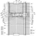
도 1은 본 발명의 일 실시예에 의한 표시 장치를 나타낸 평면도이
도 2는 본 발명의 일 실시예에 의한 표시 장치의 한 화소를 나타낸 평면도이다.
도 3은 도 1의 III-III선을 따라 나타낸 본 발명의 일 실시예에 의한 표시 장치의 일부를 나타낸 단면도이다.
도 4는 도 1의 IV-IV선을 따라 나타낸 본 발명의 일 실시예에 의한 표시 장치의 일부를 나타낸 단면도이다.
도 5 내지 도 10은 본 발명의 일 실시예에 의한 표시 장치의 제조 방법을 나타낸 공정 단면도이다.
도 11은 본 발명의 일 실시예에 의한 표시 장치를 나타낸 평면도이다.
도 12는 본 발명의 일 실시예에 의한 표시 장치의 한 화소를 나타낸 평면도이다.
도 13은 도 11의 XIII-XIII선을 따라 나타낸 본 발명의 일 실시예에 의한 표시 장치의 일부를 나타낸 단면도이다.
도 14 내지 도 17은 본 발명의 일 실시예에 의한 표시 장치의 제조 방법을 나타낸 공정 단면도이다.
도 18 내지 도 20은 본 발명의 일 실시예에 의한 표시 장치의 제조 방법을 나타낸 공정 단면도이다.1 is a plan view showing a display device according to an embodiment of the present invention;
2 is a plan view showing one pixel of a display device according to an embodiment of the present invention.
3 is a cross-sectional view illustrating a part of a display device according to an embodiment of the present invention along line III-III in FIG.
4 is a cross-sectional view illustrating a portion of a display device according to an embodiment of the present invention along line IV-IV of FIG.
5 to 10 are process cross-sectional views illustrating a method of manufacturing a display device according to an embodiment of the present invention.
11 is a plan view showing a display device according to an embodiment of the present invention.
12 is a plan view showing one pixel of a display device according to an embodiment of the present invention.
13 is a cross-sectional view illustrating a portion of a display device according to an embodiment of the present invention along line XIII-XIII in FIG.
14 to 17 are process cross-sectional views illustrating a method of manufacturing a display device according to an embodiment of the present invention.
18 to 20 are process cross-sectional views illustrating a method of manufacturing a display device according to an embodiment of the present invention.
이하에서 첨부한 도면을 참고로 하여 본 발명의 실시예에 대하여 본 발명이 속하는 기술 분야에서 통상의 지식을 가진 자가 용이하게 실시할 수 있도록 상세히 설명한다. 그러나 본 발명은 여러 가지 상이한 형태로 구현될 수 있으며 여기에서 설명하는 실시예에 한정되지 않는다.Hereinafter, exemplary embodiments of the present invention will be described in detail with reference to the accompanying drawings, which will be readily apparent to those skilled in the art to which the present invention pertains. The present invention may, however, be embodied in many different forms and should not be construed as limited to the embodiments set forth herein.
도면에서 여러 층 및 영역을 명확하게 표현하기 위하여 두께를 확대하여 나타내었다. 명세서 전체를 통하여 유사한 부분에 대해서는 동일한 도면 부호를 붙였다. 층, 막, 영역, 판 등의 부분이 다른 부분 "위에" 있다고 할 때, 이는 다른 부분 "바로 위에" 있는 경우뿐 아니라 그 중간에 또 다른 부분이 있는 경우도 포함한다. 반대로 어떤 부분이 다른 부분 "바로 위에" 있다고 할 때에는 중간에 다른 부분이 없는 것을 뜻한다.
In the drawings, the thickness is enlarged to clearly represent the layers and regions. Like parts are designated with like reference numerals throughout the specification. It will be understood that when an element such as a layer, film, region, plate, or the like is referred to as being "on" another portion, it includes not only the element directly over another element, Conversely, when a part is "directly over" another part, it means that there is no other part in the middle.
먼저, 첨부된 도면을 참조하여 본 발명의 일 실시예에 의한 표시 장치에 대해 개략적으로 설명하면 다음과 같다.First, a display device according to an embodiment of the present invention will be described with reference to the accompanying drawings.
도 1은 본 발명의 일 실시예에 의한 표시 장치를 나타낸 평면도이고, 편의상 도 1에는 일부 구성 요소만 도시되어 있다.FIG. 1 is a plan view showing a display device according to an embodiment of the present invention. For convenience, only some components are shown in FIG.
본 발명의 일 실시예에 의한 표시 장치는 유리 또는 플라스틱 등과 같은 재료로 만들어진 기판(110), 기판(110) 위에 형성되어 있는 지붕층(360)을 포함한다.A display device according to an embodiment of the present invention includes a
기판(110)은 복수의 화소 영역(PX)을 포함한다. 복수의 화소 영역(PX)은 복수의 화소 행과 복수의 화소 열을 포함하는 매트릭스 형태로 배치되어 있다. 각 화소 영역(PX)은 제1 부화소 영역(PXa) 및 제2 부화소 영역(PXb)를 포함할 수 있다. 제1 부화소 영역(PXa) 및 제2 부화소 영역(PXb)은 상하로 배치될 수 있다.The
제1 부화소 영역(PXa)과 제2 부화소 영역(PXb) 사이에는 화소 행 방향을 따라서 제1 골짜기(V1)가 위치하고 있고, 복수의 화소 열 사이에는 제2 골짜기(V2)가 위치하고 있다.The first valley V1 is located between the first sub pixel region PXa and the second sub pixel region PXb along the pixel row direction and the second valley V2 is located between the plurality of pixel columns.
지붕층(360)은 복수의 화소 행을 따라 형성될 수 있다. 이때, 제1 골짜기(V1)에서는 지붕층(360)이 제거되어 지붕층(360) 아래에 위치하는 구성 요소가 외부로 노출될 수 있도록 주입구(307)가 형성되어 있다.The
각각의 제1 부화소 영역(PXa) 및 제2 부화소 영역(PXb)은 하나의 주입구(307)를 포함할 수 있다. 예를 들면, 제1 부화소 영역(PXa)의 하측변에 대응하여 주입구(307)가 형성되고, 제2 부화소 영역(PXb)의 상측변에 대응하여 주입구(307)가 형성되어, 두 주입구(307)는 서로 마주보게 된다.Each of the first sub-pixel region PXa and the second sub-pixel region PXb may include one
주입구(307)에는 구슬 부재(400)가 형성되어 있다. 구슬 부재(400)는 각각의 주입구(307)에 형성될 수 있다. 예를 들면, 제1 부화소 영역(PXa)에 형성되어 있는 주입구(307)에 3개의 구슬 부재(400)가 형성되고, 제2 부화소 영역(PXb)에 형성되어 있는 주입구(307)에 3개의 구슬 부재(400)가 형성될 수 있다. 다만, 이는 예시에 불과하여, 각 주입구(307)에 형성되어 있는 구슬 부재(400)의 개수는 서로 상이할 수 있다. 또한, 일부 주입구(307)에는 구슬 부재(400)가 형성되고, 나머지 주입구(307)에는 구슬 부재(400)가 형성되지 않을 수도 있다.A
이어, 도 1 내지 도 4를 참조하여 본 발명의 일 실시예에 의한 표시 장치의 한 화소에 대하여 설명하면 다음과 같다.Next, a pixel of a display device according to an embodiment of the present invention will be described with reference to FIGS. 1 to 4. FIG.
도 2는 본 발명의 일 실시예에 의한 표시 장치의 한 화소를 나타낸 평면도이고, 도 3은 도 1의 III-III선을 따라 나타낸 본 발명의 일 실시예에 의한 표시 장치의 일부를 나타낸 단면도이며, 도 4는 도 1의 IV-IV선을 따라 나타낸 본 발명의 일 실시예에 의한 표시 장치의 일부를 나타낸 단면도이다.FIG. 2 is a plan view showing one pixel of a display device according to an embodiment of the present invention, FIG. 3 is a cross-sectional view showing a part of a display device according to an embodiment of the present invention along line III-III of FIG. 1 And FIG. 4 is a cross-sectional view illustrating a part of the display device according to an embodiment of the present invention, taken along the line IV-IV in FIG.
도 1 내지 도 4를 참조하면, 기판(110) 위에 복수의 게이트선(121), 복수의 감압 게이트선(123) 및 복수의 유지 전극선(131)을 포함하는 복수의 게이트 도전체가 형성되어 있다.1 to 4, a plurality of gate conductors including a plurality of
게이트선(121) 및 감압 게이트선(123)은 주로 가로 방향으로 뻗어 있으며 게이트 신호를 전달한다. 게이트 도전체는 게이트선(121)으로부터 위아래로 돌출한 제1 게이트 전극(124h) 및 제2 게이트 전극(124l)을 더 포함하고, 감압 게이트선(123)으로부터 위로 돌출한 제3 게이트 전극(124c)을 더 포함한다. 제1 게이트 전극(124h) 및 제2 게이트 전극(124l)은 서로 연결되어 하나의 돌출부를 이룬다. 이때, 제1, 제2, 및 제3 게이트 전극(124h, 124l, 124c)의 돌출 형태는 변경이 가능하다.The
유지 전극선(131)도 주로 가로 방향으로 뻗어 있으며 공통 전압(Vcom) 등의 정해진 전압을 전달한다. 유지 전극선(131)은 위 아래로 돌출한 유지 전극(129), 게이트선(121)과 실질적으로 수직하게 아래로 뻗은 한 쌍의 세로부(134) 및 한 쌍의 세로부(134)의 끝을 서로 연결하는 가로부(127)를 포함한다. 가로부(127)는 아래로 확장된 용량 전극(137)을 포함한다.The sustain
게이트 도전체(121, 123, 124h, 124l, 124c, 131) 위에는 게이트 절연막(gate insulating layer)(140)이 형성되어 있다. 게이트 절연막(140)은 실리콘 질화물(SiNx), 실리콘 산화물(SiOx) 등과 같은 무기 절연 물질로 이루어질 수 있다. 또한, 게이트 절연막(140)은 단일막 또는 다중막으로 이루어질 수 있다.A
게이트 절연막(140) 위에는 제1 반도체(154h), 제2 반도체(154l), 및 제3 반도체(154c)가 형성되어 있다. 제1 반도체(154h)는 제1 게이트 전극(124h) 위에 위치할 수 있고, 제2 반도체(154l)는 제2 게이트 전극(124l) 위에 위치할 수 있으며, 제3 반도체(154c)는 제3 게이트 전극(124c) 위에 위치할 수 있다. 제1 반도체(154h)와 제2 반도체(154l)는 서로 연결될 수 있고, 제2 반도체(154l)와 제3 반도체(154c)도 서로 연결될 수 있다. 또한, 제1 반도체(154h)는 데이터선(171)의 아래까지 연장되어 형성될 수도 있다. 제1 내지 제3 반도체(154h, 154l, 154c)는 비정질 실리콘(amorphous silicon), 다결정 실리콘(polycrystalline silicon), 금속 산화물(metal oxide) 등으로 이루어질 수 있다.A
제1 내지 제3 반도체(154h, 154l, 154c) 위에는 각각 저항성 접촉 부재(ohmic contact)(도시하지 않음)가 더 형성될 수 있다. 저항성 접촉 부재는 실리사이드(silicide) 또는 n형 불순물이 고농도로 도핑되어 있는 n+ 수소화 비정질 규소 따위의 물질로 만들어질 수 있다.Resistive ohmic contacts (not shown) may further be formed on the first to
제1 내지 제3 반도체(154h, 154l, 154c) 위에는 데이터선(data line)(171), 제1 소스 전극(173h), 제2 소스 전극(173l), 제3 소스 전극(173c), 제1 드레인 전극(175h), 제2 드레인 전극(175l), 및 제3 드레인 전극(175c)을 포함하는 데이터 도전체가 형성되어 있다.A
데이터선(171)은 데이터 신호를 전달하며 주로 세로 방향으로 뻗어 게이트선(121) 및 감압 게이트선(123)과 교차한다. 각 데이터선(171)은 제1 게이트 전극(124h) 및 제2 게이트 전극(124l)을 향하여 뻗으며 서로 연결되어 있는 제1 소스 전극(173h) 및 제2 소스 전극(173l)을 포함한다.The
제1 드레인 전극(175h), 제2 드레인 전극(175l) 및 제3 드레인 전극(175c)은 넓은 한 쪽 끝 부분과 막대형인 다른 쪽 끝 부분을 포함한다. 제1 드레인 전극(175h) 및 제2 드레인 전극(175l)의 막대형 끝 부분은 제1 소스 전극(173h) 및 제2 소스 전극(173l)으로 일부 둘러싸여 있다. 제2 드레인 전극(175l)의 넓은 한 쪽 끝 부분은 다시 연장되어 'U'자 형태로 굽은 제3 소스 전극(173c)을 이룬다. 제3 드레인 전극(175c)의 넓은 끝 부분(177c)은 용량 전극(137)과 중첩하여 감압 축전기(Cstd)를 이루며, 막대형 끝 부분은 제3 소스 전극(173c)으로 일부 둘러싸여 있다.The
제1 게이트 전극(124h), 제1 소스 전극(173h), 및 제1 드레인 전극(175h)은 제1 반도체(154h)와 함께 제1 박막 트랜지스터(Qh)를 형성하고, 제2 게이트 전극(124l), 제2 소스 전극(173l), 및 제2 드레인 전극(175l)은 제2 반도체(154l)와 함께 제2 박막 트랜지스터(Ql)를 형성하며, 제3 게이트 전극(124c), 제3 소스 전극(173c), 및 제3 드레인 전극(175c)은 제3 반도체(154c)와 함께 제3 박막 트랜지스터(Qc)를 형성한다.The
제1 반도체(154h), 제2 반도체(154l), 및 제3 반도체(154c)는 서로 연결되어 선형으로 이루어질 수 있으며, 소스 전극(173h, 173l, 173c)과 드레인 전극(175h, 175l, 175c) 사이의 채널 영역을 제외하고는 데이터 도전체(171, 173h, 173l, 173c, 175h, 175l, 175c) 및 그 하부의 저항성 접촉 부재와 실질적으로 동일한 평면 모양을 가질 수 있다.The
제1 반도체(154h)에는 제1 소스 전극(173h)과 제1 드레인 전극(175h) 사이에서 제1 소스 전극(173h) 및 제1 드레인 전극(175h)에 의해 가리지 않고 노출된 부분이 있고, 제2 반도체(154l)에는 제2 소스 전극(173l)과 제2 드레인 전극(175l) 사이에서 제2 소스 전극(173l) 및 제2 드레인 전극(175l)에 의해 가리지 않고 노출된 부분이 있으며, 제3 반도체(154c)에는 제3 소스 전극(173c)과 제3 드레인 전극(175c) 사이에서 제3 소스 전극(173c) 및 제3 드레인 전극(175c)에 의해 가리지 않고 노출된 부분이 있다.The
데이터 도전체(171, 173h, 173l, 173c, 175h, 175l, 175c) 및 각 소스 전극(173h/173l/173c)과 각 드레인 전극(175h/175l/175c) 사이로 노출되어 있는 반도체(154h, 154l, 154c) 위에는 보호막(180)이 형성되어 있다. 보호막(180)은 유기 절연 물질 또는 무기 절연 물질로 이루어질 수 있으며, 단일막 또는 다중막으로 형성될 수 있다.The
보호막(180) 위에는 각 화소 영역(PX) 내에 색필터(230)가 형성되어 있다. 각 색필터(230)는 적색, 녹색 및 청색의 삼원색 등 기본색(primary color) 중 하나를 표시할 수 있다. 색필터(230)는 적색, 녹색, 및 청색의 삼원색에 한정되지 아니하고, 청록색(cyan), 자홍색(magenta), 옐로(yellow), 화이트 계열의 색 등을 표시할 수도 있다. 도시된 바와 달리 색필터(230)는 이웃하는 데이터선(171) 사이를 따라서 열 방향으로 길게 뻗을 수도 있다.A
이웃하는 색필터(230) 사이의 영역에는 차광 부재(220)가 형성되어 있다. 차광 부재(220)는 화소 영역(PX)의 경계부와 박막 트랜지스터 위에 형성되어 빛샘을 방지할 수 있다. 색필터(230)는 각 제1 부화소 영역(PXa)과 제2 부화소 영역(PXb)에 형성되고, 제1 부화소 영역(PXa)과 제2 부화소 영역(PXb) 사이에는 차광 부재(220)가 형성될 수 있다. A
차광 부재(220)는 게이트선(121) 및 감압 게이트선(123)을 따라 뻗어 위아래로 확장되어 있으며 제1 박막 트랜지스터(Qh), 제2 박막 트랜지스터(Ql) 및 제3 박막 트랜지스터(Qc) 등이 위치하는 영역을 덮는 가로 차광 부재(220a)와 데이터선(171)을 따라 뻗어 있는 세로 차광 부재(220b)를 포함한다. 즉, 가로 차광 부재(220a)는 제1 골짜기(V1)에 형성되고, 세로 차광 부재(220b)는 제2 골짜기(V2)에 형성될 수 있다. 색필터(230)와 차광 부재(220)는 일부 영역에서 서로 중첩될 수도 있다.The
색필터(230) 및 차광 부재(220) 위에는 제1 절연층(240)이 더 형성될 수 있다. 제1 절연층(240)은 실리콘 질화물(SiNx), 실리콘 산화물(SiOx) 등과 같은 무기 절연 물질로 이루어질 수 있다. 제1 절연층(240)은 유기 물질로 이루어진 색필터(230) 및 차광 부재(220)를 보호하는 역할을 하며, 필요에 따라 생략될 수도 있다.The first insulating
제1 절연층(240), 차광 부재(220), 보호막(180)에는 제1 드레인 전극(175h)의 넓은 끝 부분과 제2 드레인 전극(175l)의 넓은 끝 부분을 각각 드러내는 복수의 제1 접촉 구멍(185h) 및 복수의 제2 접촉 구멍(185l)이 형성되어 있다.The first insulating
제1 절연층(240) 위에는 화소 전극(191)이 형성되어 있다. 화소 전극(191)은 인듐-주석 산화물(ITO, Indium Tin Oxide), 인듐-아연 산화물(IZO, Indium Zinc Oxide) 등과 같은 투명한 금속 물질로 이루어질 수 있다.A
화소 전극(191)은 게이트선(121) 및 감압 게이트선(123)을 사이에 두고 서로 분리되어, 게이트선(121) 및 감압 게이트선(123)을 중심으로 화소 영역(PX)의 위와 아래에 배치되어 열 방향으로 이웃하는 제1 부화소 전극(191h)과 제2 부화소 전극(191l)을 포함한다. 즉, 제1 부화소 전극(191h)과 제2 부화소 전극(191l)은 제1 골짜기(V1)를 사이에 두고 분리되어 있으며, 제1 부화소 전극(191h)은 제1 부화소 영역(PXa)에 위치하고, 제2 부화소 전극(191l)은 제2 부화소 영역(PXb)에 위치한다.The
제1 부화소 전극(191h) 및 제2 부화소 전극(191l)은 제1 접촉 구멍(185h) 및 제2 접촉 구멍(185l)을 통하여 각기 제1 드레인 전극(175h) 및 제2 드레인 전극(175l)과 연결되어 있다. 따라서, 제1 박막 트랜지스터(Qh) 및 제2 박막 트랜지스터(Ql)가 온 상태일 때 제1 드레인 전극(175h) 및 제2 드레인 전극(175l)으로부터 데이터 전압을 인가 받는다.The
제1 부화소 전극(191h) 및 제2 부화소 전극(191l) 각각의 전체적인 모양은 사각형이며 제1 부화소 전극(191h) 및 제2 부화소 전극(191l) 각각은 가로 줄기부(193h, 193l), 가로 줄기부(193h, 193l)와 교차하는 세로 줄기부(192h, 192l)로 이루어진 십자형 줄기부를 포함한다. 또한, 제1 부화소 전극(191h) 및 제2 부화소 전극(191l)은 각각 복수의 미세 가지부(194h, 194l), 부화소 전극(191h, 191l)의 가장자리 변에서 아래 또는 위로 돌출된 돌출부(197h, 197l)를 포함한다.The
화소 전극(191)은 가로 줄기부(193h, 193l)와 세로 줄기부(192h, 192l)에 의해 4개의 부영역으로 나뉘어진다. 미세 가지부(194h, 194l)는 가로 줄기부(193h, 193l) 및 세로 줄기부(192h, 192l)로부터 비스듬하게 뻗어 있으며 그 뻗는 방향은 게이트선(121) 또는 가로 줄기부(193h, 193l)와 대략 45도 또는 135도의 각을 이룰 수 있다. 또한 이웃하는 두 부영역의 미세 가지부(194h, 194l)가 뻗어 있는 방향은 서로 직교할 수 있다.The
본 실시예에서 제1 부화소 전극(191h)은 외곽을 둘러싸는 외곽 줄기부를 더 포함하고, 제2 부화소 전극(191l)은 상단 및 하단에 위치하는 가로부 및 제1 부화소 전극(191h)의 좌우에 위치하는 좌우 세로부(198)를 더 포함한다. 좌우 세로부(198)는 데이터선(171)과 제1 부화소 전극(191h) 사이의 용량성 결합, 즉 커플링을 방지할 수 있다.In this embodiment, the
상기에서 설명한 화소 영역의 배치 형태, 박막 트랜지스터의 구조 및 화소 전극의 형상은 하나의 예에 불과하며, 본 발명은 이에 한정되지 아니하고 다양한 변형이 가능하다.The arrangement of the pixel region, the structure of the thin film transistor, and the shape of the pixel electrode described above are only examples, and the present invention is not limited thereto and various modifications are possible.
화소 전극(191) 위에는 화소 전극(191)으로부터 일정한 거리를 가지고 이격되도록 공통 전극(270)이 형성되어 있다. 화소 전극(191)과 공통 전극(270) 사이에는 미세 공간(microcavity, 305)이 형성되어 있다. 즉, 미세 공간(305)은 화소 전극(191) 및 공통 전극(270)에 의해 둘러싸여 있다. 미세 공간(305)의 폭과 넓이는 표시 장치의 크기 및 해상도에 따라 다양하게 변경될 수 있다. 다만, 본 발명은 이에 한정되지 아니하고 공통 전극(270)이 화소 전극(191)과 절연막을 사이에 두고 형성될 수도 있다. 이때, 화소 전극(191)과 공통 전극(270) 사이에는 미세 공간(305)이 형성되지 않고, 미세 공간(305)은 공통 전극(270) 위에 형성될 수 있다.A
공통 전극(270)은 인듐-주석 산화물(ITO, Indium Tin Oxide), 인듐-아연 산화물(IZO, Indium Zinc Oxide) 등과 같은 투명한 금속 물질로 이루어질 수 있다. 공통 전극(270)에는 일정한 전압이 인가될 수 있고, 화소 전극(191)과 공통 전극(270) 사이에 전계가 형성될 수 있다.The
화소 전극(191) 위에는 제1 배향막(11)이 형성되어 있다. 제1 배향막(11)은 화소 전극(191)에 의해 덮여있지 않은 제1 절연층(240) 바로 위에도 형성될 수 있다.A
제1 배향막(11)과 마주보도록 공통 전극(270) 아래에는 제2 배향막(21)이 형성되어 있다.A
제1 배향막(11)과 제2 배향막(21)은 수직 배향막으로 이루어질 수 있고, 폴리 아믹산(Polyamic acid), 폴리 실록산(Polysiloxane), 폴리 이미드(Polyimide) 등의 배향 물질로 이루어질 수 있다. 제1 및 제2 배향막(11, 21)은 화소 영역(PX)의 가장자리에서 서로 연결될 수 있다.The
화소 전극(191)과 공통 전극(270) 사이에 위치한 미세 공간(305) 내에는 액정 분자(310)들로 이루어진 액정층이 형성되어 있다. 액정 분자(310)들은 음의 유전율 이방성을 가지며, 전계가 인가되지 않은 상태에서 기판(110)에 수직한 방향으로 서 있을 수 있다. 즉, 수직 배향이 이루어질 수 있다.A liquid crystal layer made of
데이터 전압이 인가된 제1 부화소 전극(191h) 및 제2 부화소 전극(191l)은 공통 전극(270)과 함께 전기장을 생성함으로써 두 전극(191, 270) 사이의 미세 공간(305) 내에 위치한 액정 분자(310)의 방향을 결정한다. 이와 같이 결정된 액정 분자(310)의 방향에 따라 액정층을 통과하는 빛의 휘도가 달라진다.The
공통 전극(270) 위에는 제2 절연층(350)이 더 형성될 수 있다. 제2 절연층(350)은 실리콘 질화물(SiNx), 실리콘 산화물(SiOx) 등과 같은 무기 절연 물질로 이루어질 수 있으며, 필요에 따라 생략될 수도 있다.A second insulating
제2 절연층(350) 위에는 지붕층(360)이 형성되어 있다. 지붕층(360)은 유기 물질로 이루어질 수 있다. 지붕층(360)의 아래에는 미세 공간(305)이 형성되어 있고, 지붕층(360)은 경화 공정에 의해 단단해져 미세 공간(305)의 형상을 유지할 수 있다. 지붕층(360)은 화소 전극(191)과 미세 공간(305)을 사이에 두고 이격되도록 형성되어 있다.A
지붕층(360)은 화소 행을 따라 각 화소 영역(PX) 및 제2 골짜기(V2)에 형성되며, 제1 골짜기(V1)에는 형성되지 않는다. 즉, 지붕층(360)은 제1 부화소 영역(PXa)과 제2 부화소 영역(PXb) 사이에는 형성되지 않는다. 각 제1 부화소 영역(PXa)과 제2 부화소 영역(PXb)에서는 각 지붕층(360)의 아래에 미세 공간(305)이 형성되어 있다. 제2 골짜기(V2)에서는 지붕층(360)의 아래에 미세 공간(305)이 형성되지 않으며, 기판(110)에 부착되도록 형성되어 있다. 따라서, 제2 골짜기(V2)에 위치하는 지붕층(360)의 두께가 각 제1 부화소 영역(PXa) 및 제2 부화소 영역(PXb)에 위치하는 지붕층(360)의 두께보다 두껍게 형성될 수 있다. 미세 공간(305)의 상부면 및 양측면은 지붕층(360)에 의해 덮여 있는 형태로 이루어지게 된다.The
지붕층(360)에는 미세 공간(305)의 일부를 노출시키는 주입구(307)가 형성되어 있다. 주입구(307)는 앞서 설명한 바와 같이 제1 부화소 영역(PXa)과 제2 부화소 영역(PXb)의 가장자리에 서로 마주보도록 형성될 수 있다. 즉, 주입구(307)는 제1 부화소 영역(PXa)의 하측 변, 제2 부화소 영역(PXb)의 상측 변에 대응하여 미세 공간(305)의 측면을 노출시키도록 형성될 수 있다.The
주입구(307)에 의해 미세 공간(305)이 노출되어 있으므로, 주입구(307)를 통해 미세 공간(305) 내부로 배향액 또는 액정 물질 등을 주입할 수 있다.Since the
주입구(307)에는 구슬 부재(400)가 형성되어 있다. 구슬 부재(400)는 구형의 형상을 가지므로, 구슬 부재(400)의 일부는 미세 공간(305)의 내부에 위치하게 되고, 나머지 일부는 미세 공간(305)의 외부에 위치하게 된다. 미세 공간(305)의 내부에 위치하는 구슬 부재(400)의 면적은 각 구슬 부재(400)마다 상이할 수 있다. 즉, 복수의 구슬 부재(400)가 각 제1 부화소 영역(PXa) 및 제2 부화소 영역(PXb)의 경계선을 기준으로 조금씩 상이하게 위치할 수 있다.A
구슬 부재(400)는 미세 공간(305)의 높이에 상응하게 형성되어, 주입구(307)에 고정되어 있다. 지붕층(360)은 주입구(307) 부근에서 하부면을 지지하는 힘이 상대적으로 약하므로 처짐 현상이 발생할 수 있다. 본 발명의 일 실시예에서는 주입구(307)에서 구슬 부재(400)가 지붕층(360)을 지지하게 되므로 이러한 처짐 현상을 방지할 수 있다.The
구슬 부재(400)의 지름은 미세 공간(305)의 높이 이상으로 이루어지는 것이 바람직하다. 구슬 부재(400)의 지름이 미세 공간(305)의 높이보다 작은 경우 구슬 부재(400)가 미세 공간(305)의 내부로 이동하게 될 수도 있다. 구슬 부재(400)가 미세 공간(305)의 내부로 이동하여 화면을 표시하는 영역에 위치하게 되면, 액정층을 통과하는 빛에 영향을 주게 되어 불량으로 시인될 수 있다. 따라서 구슬 부재(400)가 미세 공간(305)의 내부로 들어가지 않도록 하기 위해서는, 구슬 부재(400)의 지름을 미세 공간(305)의 높이와 동일하거나 더 크게 형성하는 것이 바람직하다.It is preferable that the diameter of the
구슬 부재(400)의 지름은 미세 공간(305)의 높이의 110% 이하로 이루어지는 것이 바람직하다. 구슬 부재(400)의 지름이 미세 공간(305)의 높이보다 과도하게 큰 경우 구슬 부재(400)가 주입구(307)에 고정되지 못할 수도 있다. 구슬 부재(400)가 주입구(307)에 고정되지 못하게 되면, 지붕층(360)을 지지하는 역할을 수행할 수 없게 된다. 따라서, 구슬 부재(400)의 지름이 미세 공간(305)의 높이와 유사하도록 형성하는 것이 바람직하다.It is preferable that the diameter of the
구슬 부재(400)의 외부 면은 제1 배향막(11) 및 제2 배향막(12)을 구성하는 배향 물질에 의해 둘러 쌓여 있을 수 있다. 즉, 배향 물질이 구슬 부재(400)를 감싸도록 형성될 수 있다. 제1 배향막(11) 및 제2 배향막(12)을 형성하는 단계에서, 배향 물질과 구슬 부재(400)를 혼합하여 주입구(307)에 공급하는 경우 배향 물질이 구슬 부재(400)의 표면에 남게 된다. 배향 물질이 경화됨에 따라 구슬 부재(400)가 주입구(307)에 더 단단하게 고정되도록 하는 역할을 할 수 있다.The outer surface of the
구슬 부재(400)가 주입구(307)에 형성됨에 따라 주입구(307)의 일부 영역을 차단하게 된다. 이때, 구슬 부재(400)는 주입구(307)의 전체 영역을 차단하지 않도록 형성하는 것이 바람직하다. 제1 배향막(11) 및 제2 배향막(12)을 형성하는 단계에서 구슬 부재(400)를 형성하는 경우, 제1 및 제2 배향막(11, 12) 형성 후 액정 물질을 주입하는 단계에서 액정 주입의 불량이 발생하는 것이 방지하기 위함이다. 따라서, 구슬 부재(400)가 주입구(307)를 차단하는 면적은 주입구(307)의 전체 면적의 1% 이상 80% 이하인 것이 바람직하다.As the
지붕층(360) 위에는 제3 절연층(370)이 더 형성될 수 있다. 제3 절연층(370)은 실리콘 질화물(SiNx), 실리콘 산화물(SiOx) 등과 같은 무기 절연 물질로 이루어질 수 있다. 제3 절연층(370)은 지붕층(360)의 상부면 및 측면을 덮도록 형성될 수 있다. 제3 절연층(370)은 유기 물질로 이루어진 지붕층(360)을 보호하는 역할을 하며, 필요에 따라 생략될 수도 있다.A third insulating
제3 절연층(370) 위에는 덮개막(390)이 형성될 수 있다. 덮개막(390)은 미세 공간(305)의 일부를 외부로 노출시키는 주입구(307)를 덮도록 형성된다. 즉, 덮개막(390)은 미세 공간(305)의 내부에 형성되어 있는 액정 분자(310)가 외부로 나오지 않도록 미세 공간(305)을 밀봉할 수 있다. 덮개막(390)은 액정 분자(310)과 접촉하게 되므로, 액정 분자(310)과 반응하지 않는 물질로 이루어지는 것이 바람직하다. 예를 들면, 덮개막(390)은 페릴렌(Parylene) 등으로 이루어질 수 있다.A
본 발명의 일 실시예에서는 주입구(307)의 일부 영역을 구슬 부재(400)가 차단하고 있으므로, 액정 분자(310)가 덮개막(390)에 의해 영향을 덜 받게 된다. 주입구(307)가 완전히 개방되어 있는 경우 덮개막(390)을 형성하는 물질이 주입구(307)의 내부로 침투하는 것을 방지하기 위해 덮개막(390)의 점도를 높게 할 경우 덮개막(390)의 평탄도가 낮아지게 된다. 본 발명의 일 실시예에서는 구슬 부재(400)에 의해 주입구(307)가 일부 차단되므로 덮개막(390)의 점도를 낮게 형성하여 덮개막(390)을 균일하게 형성할 수 있다. 예를 들면, 덮개막(390)의 점도는 1000cp 이하일 수 있으며, 30cp 이상이고, 100cp 이하의 범위를 가지도록 할 수 있다.The
덮개막(390)은 이중막, 삼중막 등과 같이 다중막으로 이루어질 수도 있다. 이중막은 서로 다른 물질로 이루어진 두 개의 층으로 이루어져 있다. 삼중막은 세 개의 층으로 이루어지고, 서로 인접하는 층의 물질이 서로 다르다. 예를 들면, 덮개막(390)은 유기 절연 물질로 이루어진 층과 무기 절연 물질로 이루어진 층을 포함할 수 있다.The
도시는 생략하였으나, 표시 장치의 상하부 면에는 편광판이 더 형성될 수 있다. 편광판은 제1 편광판 및 제2 편광판으로 이루어질 수 있다. 제1 편광판은 기판(110)의 하부 면에 부착되고, 제2 편광판은 덮개막(390) 위에 부착될 수 있다.
Although not shown, a polarizing plate may be further formed on the upper and lower surfaces of the display device. The polarizing plate may comprise a first polarizing plate and a second polarizing plate. The first polarizing plate may be attached to the lower surface of the
다음으로, 도 5 내지 도 10을 참조하여 본 발명의 일 실시예에 의한 표시 장치의 제조 방법에 대해 설명하면 다음과 같다. 아울러, 도 1 내지 도 4를 함께 참조하여 설명한다.Next, a method of manufacturing a display device according to an embodiment of the present invention will be described with reference to FIGS. 5 to 10. FIG. 1 to 4 together.
도 5 내지 도 10은 본 발명의 일 실시예에 의한 표시 장치의 제조 방법을 나타낸 공정 단면도이다.5 to 10 are process cross-sectional views illustrating a method of manufacturing a display device according to an embodiment of the present invention.
먼저, 도 5에 도시된 바와 같이, 유리 또는 플라스틱 등으로 이루어진 기판(110) 위에 일방향으로 뻗어있는 게이트선(121)과 감압 게이트선(123)을 형성하고, 게이트선(121)으로부터 돌출되는 제1 게이트 전극(124h), 제2 게이트 전극(124l), 및 제3 게이트 전극(124c)을 형성한다.5, a
또한, 게이트선(121), 감압 게이트선(123), 및 제1 내지 제3 게이트 전극(124h, 124l, 124c)와 이격되도록 유지 전극선(131)을 함께 형성할 수 있다.The
이어, 게이트선(121), 감압 게이트선(123), 제1 내지 제3 게이트 전극(124h, 124l, 124c), 및 유지 전극선(131)을 포함한 기판(110) 위의 전면에 실리콘 산화물(SiOx) 또는 실리콘 질화물(SiNx)과 같은 무기 절연 물질을 이용하여 게이트 절연막(140)을 형성한다. 게이트 절연막(140)은 단일막 또는 다중막으로 형성할 수 있다.Next, silicon oxide (SiOx) is deposited on the entire surface of the
이어, 게이트 절연막(140) 위에 비정질 실리콘(amorphous silicon), 다결정 실리콘(polycrystalline silicon), 금속 산화물(metal oxide) 등과 같은 반도체 물질을 증착한 후 이를 패터닝하여 제1 반도체(154h), 제2 반도체(154l), 및 제3 반도체(154c)를 형성한다. 제1 반도체(154h)는 제1 게이트 전극(124h) 위에 위치하도록 형성하고, 제2 반도체(154l)는 제2 게이트 전극(124l) 위에 위치하도록 형성하며, 제3 반도체(154c)는 제3 게이트 전극(124c) 위에 위치하도록 형성할 수 있다.Next, a semiconductor material such as amorphous silicon, polycrystalline silicon, metal oxide, or the like is deposited on the
이어, 금속 물질을 증착한 후 이를 패터닝하여 타방향으로 뻗어있는 데이터선(171)을 형성한다. 금속 물질은 단일막 또는 다중막으로 이루어질 수 있다.Then, a metal material is deposited and patterned to form a
또한, 데이터선(171)으로부터 제1 게이트 전극(124h) 위로 돌출되는 제1 소스 전극(173h) 및 제1 소스 전극(173h)과 이격되는 제1 드레인 전극(175h)을 함께 형성한다. 또한, 제1 소스 전극(173h)과 연결되어 있는 제2 소스 전극(173l) 및 제2 소스 전극(173l)과 이격되는 제2 드레인 전극(175l)을 함께 형성한다. 또한, 제2 드레인 전극(175l)으로부터 연장되어 있는 제3 소스 전극(173c) 및 제3 소스 전극(173c)과 이격되는 제3 드레인 전극(175c)을 함께 형성한다.A
반도체 물질과 금속 물질을 연속으로 증착한 후 이를 동시에 패터닝하여 제1 내지 제3 반도체(154h, 154l, 154c), 데이터선(171), 제1 내지 제3 소스 전극(173h, 173l, 173c), 및 제1 내지 제3 드레인 전극(175h, 175l, 175c)을 형성할 수도 있다. 이때, 제1 반도체(154h)는 데이터선(171)의 아래까지 연장되어 형성된다.The first to
제1/제2/제3 게이트 전극(124h/124l/124c), 제1/제2/제3 소스 전극(173h/173l/173c), 및 제1/제2/제3 드레인 전극(175h/175l/175c)은 제1/제2/제3 반도체(154h/154l/154c)와 함께 각각 제1/제2/제3 박막 트랜지스터(thin film transistor, TFT)(Qh/Ql/Qc)를 구성한다.Second and
이어, 데이터선(171), 제1 내지 제3 소스 전극(173h, 173l, 173c), 제1 내지 제3 드레인 전극(175h, 175l, 175c), 및 각 소스 전극(173h/173l/173c)과 각 드레인 전극(175h/175l/175c) 사이로 노출되어 있는 반도체(154h, 154l, 154c) 위에 보호막(180)을 형성한다. 보호막(180)은 유기 절연 물질 또는 무기 절연 물질로 이루어질 수 있으며, 단일막 또는 다중막으로 형성될 수 있다.Next, the
이어, 보호막(180) 위의 각 화소 영역(PX) 내에 색필터(230)를 형성한다. 색필터(230)는 각 제1 부화소 영역(PXa)과 제2 부화소 영역(PXb)에 형성하고, 제1 골짜기(V1)에는 형성하지 않을 수 있다. 또한, 복수의 화소 영역(PX)의 열 방향을 따라 동일한 색의 색필터(230)를 형성할 수 있다. 세 가지 색의 색필터(230)를 형성하는 경우 제1 색의 색필터(230)를 먼저 형성한 후 마스크를 쉬프트 시켜 제2 색의 색필터(230)를 형성할 수 있다. 이어, 제2 색의 색필터(230)를 형성한 후 마스크를 쉬프트시켜 제3 색의 색필터를 형성할 수 있다.Next, a
이어, 보호막(180) 위의 각 화소 영역(PX)의 경계부 및 박막 트랜지스터 위에 차광 부재(220)를 형성한다. 제1 부화소 영역(PXa)과 제2 부화소 영역(PXb)의 사이에 위치하는 제1 골짜기(V1)에도 차광 부재(220)를 형성할 수 있다.Next, the
상기에서 색필터(230)를 형성한 후 차광 부재(220)를 형성하는 것으로 설명하였으나, 본 발명은 이에 한정되지 아니하고 차광 부재(220)를 먼저 형성한 후 색필터(230)를 형성할 수도 있다.The
이어, 색필터(230) 및 차광 부재(220) 위에 실리콘 질화물(SiNx), 실리콘 산화물(SiOx) 등과 같은 무기 절연 물질로 제1 절연층(240)을 형성한다.The first insulating
이어, 보호막(180), 차광 부재(220), 및 제1 절연층(240)을 식각하여 제1 드레인 전극(175h)의 일부가 노출되도록 제1 접촉 구멍(185h)을 형성하고, 제2 드레인 전극(175l)의 일부가 노출되도록 제2 접촉 구멍(185l)을 형성한다.The
이어, 제1 절연층(240) 위에 인듐-주석 산화물(ITO, Indium Tin Oxide), 인듐-아연 산화물(IZO, Indium Zinc Oxide) 등과 같은 투명한 금속 물질을 증착한 후 패터닝하여 제1 부화소 영역(PXa) 내에 제1 부화소 전극(191h)을 형성하고, 제2 부화소 영역(PXb) 내에 제2 부화소 전극(191l)을 형성한다. 제1 부화소 전극(191h)과 제2 부화소 전극(191l)은 제1 골짜기(V1)를 사이에 두고 분리되어 있다. 제1 부화소 전극(191h)은 제1 접촉 구멍(185h)을 통해 제1 드레인 전극(175h)과 연결되도록 형성하고, 제2 부화소 전극(191l)은 제2 접촉 구멍(185l)을 통해 제2 드레인 전극(175l)과 연결되도록 형성한다.A transparent metal material such as indium tin oxide (ITO), indium zinc oxide (IZO), or the like is deposited on the first insulating
제1 부화소 전극(191h) 및 제2 부화소 전극(191l) 각각에 가로 줄기부(193h, 193l), 가로 줄기부(193h, 193l)와 교차하는 세로 줄기부(192h, 192l)를 형성한다. 또한, 가로 줄기부(193h, 193l) 및 세로 줄기부(192h, 192l)로부터 비스듬하게 뻗어있는 복수의 미세 가지부(194h, 194l)를 형성한다.The vertical
도 6에 도시된 바와 같이, 화소 전극(191) 위에 감광성 유기 물질을 도포하고, 포토 공정을 통해 희생층(300)을 형성한다.6, a photosensitive organic material is applied on the
희생층(300)은 복수의 화소 열을 따라 연결되도록 형성된다. 즉, 희생층(300)은 각 화소 영역(PX)을 덮도록 형성되고, 제1 부화소 영역(PXa)과 제2 부화소 영역(PXb) 사이에 위치한 제1 골짜기(V1)를 덮도록 형성된다.The
이어, 희생층(300) 위에 인듐-주석 산화물(ITO, Indium Tin Oxide), 인듐-아연 산화물(IZO, Indium Zinc Oxide) 등과 같은 투명한 금속 물질을 증착하여 공통 전극(270)을 형성한다.A transparent electrode material such as indium tin oxide (ITO), indium zinc oxide (IZO), or the like is deposited on the
이어, 공통 전극(270) 위에 실리콘 산화물 또는 실리콘 질화물과 같은 무기 절연 물질로 제2 절연층(350)을 형성할 수 있다.Next, the second insulating
이어, 제2 절연층(350) 위에 유기 물질로 지붕층(360)을 형성한다.Next, a
도 7에 도시된 바와 같이, 지붕층(360)을 패터닝하여 제1 골짜기(V1) 에 위치하는 지붕층(360)을 제거할 수 있다. 이에 따라 지붕층(360)은 복수의 화소 행을 따라 연결되는 형태로 이루어지게 된다.As shown in FIG. 7, the
이어, 지붕층(360) 위에 실리콘 질화물(SiNx), 실리콘 산화물(SiOx) 등과 같은 무기 절연 물질로 제3 절연층(370)을 형성할 수 있다. 제3 절연층(370)은 패터닝된 지붕층(360) 위에 형성되므로 지붕층(360)의 측면을 덮어 보호할 수 있다.The third
도 8에 도시된 바와 같이, 제3 절연층(370), 제2 절연층(350), 공통 전극(270)을 패터닝하여, 제1 골짜기(V1)에 위치하는 제3 절연층(370), 제2 절연층(350), 및 공통 전극(270)을 제거한다.8, the third insulating
지붕층(360)과 공통 전극(270)을 패터닝함에 따라 제1 골짜기(V1)에 위치한 희생층(300)이 외부로 노출된다.As the
이어, 희생층(300)이 노출된 기판(110) 위에 현상액을 공급하여 희생층(300)을 전면 제거하거나, 애싱(ashing) 공정을 이용하여 희생층(300)을 전면 제거한다.Next, the
희생층(300)이 제거되면, 희생층(300)이 위치하였던 자리에 미세 공간(305)이 생긴다.When the
화소 전극(191)과 공통 전극(270)은 미세 공간(305)을 사이에 두고 서로 이격되고, 화소 전극(191)과 지붕층(360)은 미세 공간(305)을 사이에 두고 서로 이격된다. 공통 전극(270)과 지붕층(360)은 미세 공간(305)의 상부면과 양측면을 덮도록 형성된다.The
지붕층(360) 및 공통 전극(270)이 제거된 부분을 통해 미세 공간(305)은 외부로 노출되어 있으며, 이를 액정 주입구(307)라 한다. 액정 주입구(307)는 제1 골짜기(V1)를 따라 형성되어 있다. 예를 들면, 주입구(307)는 제1 부화소 영역(PXa)과 제2 부화소 영역(PXb)의 가장자리에 서로 마주보도록 형성될 수 있다. 즉, 주입구(307)는 제1 부화소 영역(PXa)의 하측 변, 제2 부화소 영역(PXb)의 상측 변에 대응하여 미세 공간(305)의 측면을 노출시키도록 형성될 수 있다. 이와 상이하게, 액정 주입구(307)가 제2 골짜기(V2)를 따라 형성되도록 할 수도 있다.The
이어, 기판(110)에 열을 가하여 지붕층(360)을 경화시킨다. 지붕층(360)에 의해 미세 공간(305)의 형상이 유지되도록 하기 위함이다. Heat is then applied to the
이어, 잉크젯 노즐(500)을 통해 구슬 부재(400)가 포함되어 있는 배향 물질(15)을 기판(110) 위에 떨어뜨려 공급한다. 이때, 구슬 부재(400)가 포함되어 있는 배향 물질(15)을 기판(110) 위의 제1 골짜기(V1)에 떨어뜨릴 수 있다.Next, the
제1 골짜기(V1)의 가장자리에서 서로 마주보도록 형성되어 있는 주입구(307)를 통해 배향 물질(15)이 미세 공간(305)의 내부로 주입된다. 미세 공간(305)의 내부 방향으로 작용하는 모세관력(capillary force)에 의해 배향 물질(15)이 미세 공간(305)의 내부로 주입되는 것이다.The
미세 공간(305)의 내부 방향으로 작용하는 모세관력은 배향 물질(15)에 섞여 있는 구슬 부재(400)에도 작용한다. 따라서, 구슬 부재(400)도 주입구(307)로 이동하게 된다. 이때, 구슬 부재(400)가 미세 공간(305)의 내부로 삽입되어 화면을 표시하는 영역에 이르지 않도록 하는 것이 바람직하다. 즉, 구슬 부재(400)의 지름을 미세 공간(305)의 높이 이상으로 하여 구슬 부재(400)가 주입구(307)의 내부로 이동하지 않도록 한다.The capillary force acting in the inward direction of the
구슬 부재(400)가 주입구(307)에 위치함에 따라 지붕층(360)의 가장자리를 지지하게 되어 지붕층(360)이 처지는 것을 방지할 수 있다.As the
구슬 부재(400)는 주입구(307)에 위치하되, 구슬 부재(400)의 일부 영역은 미세 공간(305)의 내부에 위치하고, 나머지 영역은 미세 공간(305)의 외부에 위치하도록 한다. 이때, 미세 공간(305)의 내부와 외부에 위치하는 영역의 크기가 유사하도록 하는 것이 구슬 부재(400)의 고정에 유리하다. 이를 위해 구슬 부재(400)의 지름은 미세 공간(305)의 높이와 유사하도록 형성하는 것이 바람직하다. 예를 들면, 구슬 부재(400)의 지름을 미세 공간(305)의 높이의 110% 이하로 할 수 있다.The
배향 물질(15)에 섞여 있는 구슬 부재(400)의 함유량에 따라 구슬 부재(400)가 주입구(307)를 차단하는 면적이 달라진다. 이때, 구슬 부재(400)가 주입구(307)의 전체 영역을 차단하지 않도록 구슬 부재(400)의 함유량을 조절하는 것이 바람직하다. 주입구(307)를 통해 액정 물질을 주입하는 후속 공정에서 액정 물질이 잘 주입되지 않는 것을 방지하기 위함이다. 따라서, 구슬 부재(400)가 주입구(307)를 차단하는 면적이 주입구(307)의 전체 면적의 1% 이상 80% 이하가 되도록 구슬 부재(400)와 배향 물질(15)의 비율을 조절하는 것이 바람직하다.The area in which the
배향 물질(15)을 미세 공간(305)으로 주입한 후 경화 공정을 진행하면 용액 성분은 증발하고, 배향 물질이 미세 공간(305) 내부의 벽면에 남게 된다.When the
따라서, 화소 전극(191) 위에 제1 배향막(11)을 형성하고, 공통 전극(270) 아래에 제2 배향막(21)을 형성할 수 있다. 제1 배향막(11)과 제2 배향막(21)은 미세 공간(305)을 사이에 두고 마주보도록 형성되고, 화소 영역(PX)의 가장자리에서는 서로 연결되도록 형성된다.Accordingly, the
이때, 제1 및 제2 배향막(11, 21)은 미세 공간(305)의 측면을 제외하고는 기판(110)에 대해 수직한 방향으로 배향이 이루어질 수 있다. 추가로 제1 및 제2 배향막(11, 21)에 UV를 조사하는 공정을 진행함으로써, 기판(110)에 대해 수평한 방향으로 배향이 이루어지도록 할 수도 있다.At this time, the first and second alignment layers 11 and 21 may be oriented in a direction perpendicular to the
이어, 잉크젯 방식 또는 디스펜싱 방식으로 액정 물질을 기판(110) 위에 떨어뜨리면, 액정 물질이 주입구(307)를 통해 미세 공간(305) 내부로 주입된다. 주입구(307)는 구슬 부재(400)에 의해 일부 영역이 차단되어 있으나, 구슬 부재(400)가 형성되어 있지 않은 영역을 통해 액정 물질이 주입될 수 있다.Then, when the liquid crystal material is dropped onto the
액정 물질을 홀수 번째 제1 골짜기(V1)를 따라 형성된 주입구(307)에는 떨어뜨리고, 짝수 번째 제1 골짜기(V1)를 따라 형성된 주입구(307)에는 떨어뜨리지 않을 수 있다. 이와 반대로, 액정 물질을 짝수 번째 제1 골짜기(V1)를 따라 형성된 주입구(307)에 떨어뜨리고, 홀수 번째 제1 골짜기(V1)를 따라 형성된 주입구(307)에는 떨어뜨리지 않을 수 있다.The liquid crystal material may be dropped on the
홀수 번째 제1 골짜기(V1)를 따라 형성된 액정 주입구(307)에 액정 물질을 떨어뜨리면 모세관력(capillary force)에 의해 액정 물질이 액정 주입구(307)를 통과하여 미세 공간(305) 내부로 들어가게 된다. 이때, 짝수 번째 제1 골짜기(V1)를 따라 형성된 액정 주입구(307)를 통해 미세 공간(305) 내부의 공기가 빠져나감으로써, 액정 물질이 미세 공간(305) 내부로 들어가게 된다.When the liquid crystal material is dropped to the liquid
또한, 액정 물질을 모든 액정 주입구(307)에 떨어뜨릴 수도 있다. 즉, 액정 물질을 홀수 번째 제1 골짜기(V1)를 따라 형성된 주입구(307)와 짝수 번째 제1 골짜기(V1)를 따라 형성된 주입구(307)에 모두 떨어뜨릴 수도 있다.In addition, the liquid crystal material may be dropped to all of the liquid
도 10에 도시된 바와 같이, 제3 절연층(370) 위에 액정 분자(310)와 반응하지 않는 물질을 증착하여 덮개막(390)을 형성한다. 덮개막(390)은 미세 공간(305)이 외부로 노출되어 있는 액정 주입구(307)를 덮도록 형성되어 미세 공간(305)을 밀봉한다.As shown in FIG. 10, a material that does not react with the
본 발명의 일 실시예에서는 주입구(307)의 일부 영역이 구슬 부재(400)에 의해 차단되어 있으므로, 액정 분자(310)가 덮개막(390)과의 접촉에 의한 영향을 적게 받는다. 따라서, 덮개막(390)의 점도를 낮출 수 있으며, 이에 따라 덮개막(390)의 평탄도를 높일 수 있다. 예를 들면, 덮개막(390)의 점도는 1000cp 이하일 수 있으며, 30cp 이상이고, 100cp 이하의 범위를 가지도록 할 수 있다.The
이어, 도시는 생략하였으나, 표시 장치의 상하부 면에 편광판을 더 부착할 수 있다. 편광판은 제1 편광판과 제2 편광판으로 이루어질 수 있다. 기판(110)의 하부 면에 제1 편광판을 부착하고, 덮개막(390) 위에 제2 편광판을 부착할 수 있다.
Although not shown, a polarizing plate may be further attached to the upper and lower surfaces of the display device. The polarizing plate may include a first polarizing plate and a second polarizing plate. A first polarizing plate may be attached to the lower surface of the
다음으로, 도 11 내지 도 13을 참조하여 본 발명의 일 실시예에 의한 표시 장치에 대해 설명하면 다음과 같다.Next, a display device according to an embodiment of the present invention will be described with reference to FIGS. 11 to 13. FIG.
도 11 내지 도 13에 도시된 본 발명의 일 실시예에 의한 표시 장치는 도 1 내지 도 4에 도시된 본 발명의 일 실시예에 의한 표시 장치와 동일한 부분이 상당하므로, 이에 대한 설명은 생략하고 차이점이 있는 부분에 대해서만 이하에서 설명한다. 앞선 실시예와 가장 큰 차이점은 구슬 부재를 배향 물질 대신 액정 물질과 혼합한다는 점이며, 이하에서 더욱 상세히 설명한다.The display device according to an embodiment of the present invention shown in FIG. 11 to FIG. 13 is equivalent to the display device according to the embodiment of the present invention shown in FIGS. 1 to 4, Only differences are described below. The biggest difference from the previous embodiment is that the bead member is mixed with a liquid crystal material instead of an alignment material, which will be described in more detail below.
도 11은 본 발명의 일 실시예에 의한 표시 장치를 나타낸 평면도이고, 도 12는 본 발명의 일 실시예에 의한 표시 장치의 한 화소를 나타낸 평면도이며, 도 13은 도 11의 XIII-XIII선을 따라 나타낸 본 발명의 일 실시예에 의한 표시 장치의 일부를 나타낸 단면도이다.FIG. 11 is a plan view showing a display device according to an embodiment of the present invention, FIG. 12 is a plan view showing a pixel of a display device according to an embodiment of the present invention, FIG. 13 is a cross-sectional view taken along line XIII- Sectional view showing a part of a display device according to an embodiment of the present invention.
도 11 내지 도 13을 참조하면, 본 발명의 일 실시예에 의한 표시 장치는 기판(110) 위에 박막 트랜지스터 및 이에 연결되어 있는 화소 전극(191)이 형성되어 있다. 화소 전극(191) 위에 미세 공간(305)을 사이에 두고 이격되도록 지붕층(360)이 형성되어 있다. 미세 공간(305)에는 액정 분자(310)들로 이루어진 액정층이 형성되어 있고, 지붕층(360) 위에는 덮개막(390)이 형성되어 미세 공간(305)을 밀봉한다.11 to 13, a display device according to an embodiment of the present invention includes a thin film transistor (TFT) and a
미세 공간(305)은 주입구(307)에 의해 외부로 노출되어 있고, 주입구(307)에는 구슬 부재(400)가 형성되어 있다. 구슬 부재(400)는 구형의 형상을 가지므로, 구슬 부재(400)의 일부는 미세 공간(305)의 내부에 위치하게 되고, 나머지 일부는 미세 공간(305)의 외부에 위치하게 된다.The
구슬 부재(400)는 미세 공간(305)의 높이에 상응하게 형성되어, 주입구(307)에 고정되므로, 지붕층(360)을 지지하여 지붕층(360) 가장자리의 처짐 현상을 방지할 수 있다.The
구슬 부재(400)의 지름은 미세 공간(305)의 높이 이상으로 이루어지고, 미세 공간(305)의 높이의 110% 이하로 이루어지는 것이 바람직하다.The diameter of the
앞선 실시예와 상이하게 배향 물질이 구슬 부재(400)를 감싸고 있지 않다. 본 실시예에서는 액정층을 형성하는 단계에서, 액정 물질과 구슬 부재(400)를 혼합하여 주입구(307)에 공급함으로써, 주입구(307)에 구슬 부재(400)가 형성되고, 액정 물질은 미세 공간(305)의 내부로 주입된다. 따라서, 미세 공간(305)의 내부에 위치하는 구슬 부재(400)의 부분은 액정 물질과 접하고 있다. 미세 공간(305)의 외부에 위치하는 구슬 부재(400)의 부분에는 액정 물질이 남아 있을 수도 있고, 세정 공정에 의해 제거될 수도 있다.The orientation material does not wrap the
구슬 부재(400)가 주입구(307)에 형성됨에 따라 주입구(307)를 차단하게 된다. 이때, 구슬 부재(400)는 주입구(307)의 일부 영역 또는 전체 영역을 차단할 수 있다. 앞선 실시예에서는 구슬 부재(400)가 주입구(307)의 전체 면적의 1% 이상 80% 이하를 차단하도록 형성하는 것이 바람직하다고 하였으며, 본 실시예에서도 동일한 수치 범위에서 차단하도록 형성할 수 있다.As the
나아가 본 실시예에서는 구슬 부재(400)가 주입구(307)를 차단하는 면적이 주입구(307)의 전체 면적의 80% 초과 100이하가 되도록 형성할 수도 있다. 즉, 구슬 부재(400)가 주입구(307)의 대부분을 차단하도록 형성할 수 있다. 이에 따라 구슬 부재(400)에 의해 액정 분자(310)의 노출을 차단할 수 있다. 따라서, 덮개막(390)을 형성할 때 액정 분자(310)에 미치는 영향을 고려하지 않아도 되므로 덮개막(390)의 점도를 더욱 낮출 수 있다. 예를 들면, 덮개막(390)의 점도는 1000cp 이하일 수 있으며, 30cp 이상이고, 100cp 이하의 범위를 가지도록 할 수 있다.Further, in this embodiment, the
더 나아가 구슬 부재(400)는 서로 마주보는 주입구(307) 사이의 영역에 더 형성될 수 있다. 즉, 제1 골짜기(V1)의 가장자리뿐만 아니라 중앙부에도 구슬 부재(400)가 형성될 수 있으며, 제1 골짜기(V1) 전체 영역을 채우도록 형성될 수도 있다. 제1 골짜기(V1)에는 미세 공간(305) 및 지붕층(360)이 형성되어 있지 않으므로, 상대적으로 화소 영역(PX)에 비해 구성 요소들의 전체 두께가 낮게 형성된다. 이러한 제1 골짜기(V1)를 구슬 부재(400)로 채움으로써, 제1 골짜기(V1)과 화소 영역(PX)의 두께 차이를 줄일 수 있다.
Further, the
다음으로, 도 14 내지 도 17을 참조하여 본 발명의 일 실시예에 의한 표시 장치의 제조 방법에 대해 설명하면 다음과 같다. 아울러, 도 11 내지 도 13을 함께 참조하여 설명한다.Next, a method of manufacturing a display device according to an embodiment of the present invention will be described with reference to FIGS. 14 to 17. FIG. 11 to 13 will be described together.
도 14 내지 도 17은 본 발명의 일 실시예에 의한 표시 장치의 제조 방법을 나타낸 공정 단면도이다.14 to 17 are process cross-sectional views illustrating a method of manufacturing a display device according to an embodiment of the present invention.
먼저, 도 14에 도시된 바와 같이, 기판(110) 위에 제1 내지 제3 박막 트랜지스터(Qh/Ql/Qc)를 형성하고, 제1 및 제2 화소 전극(191h, 191l)을 형성한다. 제1 및 제2 화소 전극(191h, 191l) 위에 희생층을 형성하고, 공통 전극(270), 제2 절연층(350), 지붕층(360), 제3 절연층(370)을 순차적으로 형성한 후 패터닝하여 주입구(307)를 형성한다. 희생층을 제거하여 미세 공간(305)을 형성한다.First, as shown in FIG. 14, first to third thin film transistors Qh / Ql / Qc are formed on a
도 15에 도시된 바와 같이, 배향 물질이 포함되어 있는 배향액을 기판(110) 위에 떨어뜨리면, 배향액이 액정 주입구(307)를 통해 미세 공간(305) 내부로 주입된다. 배향액을 미세 공간(305)의 내부로 주입한 후 경화 공정을 진행하면 용액 성분은 증발하고, 배향 물질이 미세 공간(305) 내부의 벽면에 남게 된다.As shown in FIG. 15, when the alignment liquid containing the alignment material is dropped on the
따라서, 화소 전극(191) 위에 제1 배향막(11)을 형성하고, 공통 전극(270) 아래에 제2 배향막(21)을 형성할 수 있다. 제1 배향막(11)과 제2 배향막(21)은 미세 공간(305)을 사이에 두고 마주보도록 형성되고, 화소 영역(PX)의 가장자리에서는 서로 연결되도록 형성된다.Accordingly, the
이때, 제1 및 제2 배향막(11, 21)은 미세 공간(305)의 측면을 제외하고는 기판(110)에 대해 수직한 방향으로 배향이 이루어질 수 있다. 추가로 제1 및 제2 배향막(11, 21)에 UV를 조사하는 공정을 진행함으로써, 기판(110)에 대해 수평한 방향으로 배향이 이루어지도록 할 수도 있다.At this time, the first and second alignment layers 11 and 21 may be oriented in a direction perpendicular to the
도 16에 도시된 바와 같이, 잉크젯 노즐(500)을 통해 구슬 부재(400)가 포함되어 있는 액정 물질(320)을 기판(110) 위에 떨어뜨려 공급한다. 이때, 구슬 부재(400)가 포함되어 있는 액정 물질(320)을 기판(110) 위의 제1 골짜기(V1)에 떨어뜨릴 수 있다.The
제1 골짜기(V1)의 가장자리에서 서로 마주보도록 형성되어 있는 주입구(307)를 통해 액정 물질(320)이 미세 공간(305)의 내부로 주입된다. 미세 공간(305)의 내부 방향으로 작용하는 모세관력(capillary force)에 의해 액정 물질(320)이 미세 공간(305)의 내부로 주입되는 것이다.The
미세 공간(305)의 내부 방향으로 작용하는 모세관력은 액정 물질(320)에 섞여 있는 구슬 부재(400)에도 작용한다. 따라서, 구슬 부재(400)도 주입구(307)로 이동하게 된다. 이때, 구슬 부재(400)가 미세 공간(305)의 내부로 삽입되어 화면을 표시하는 영역에 이르지 않도록 하는 것이 바람직하다. 즉, 구슬 부재(400)의 지름을 미세 공간(305)의 높이 이상으로 하여 구슬 부재(400)가 주입구(307)의 내부로 이동하지 않도록 한다.The capillary force acting in the inner direction of the
구슬 부재(400)가 주입구(307)에 위치함에 따라 지붕층(360)의 가장자리를 지지하게 되어 지붕층(360)이 처지는 것을 방지할 수 있다.As the
구슬 부재(400)는 주입구(307)에 위치하되, 구슬 부재(400)의 일부 영역은 미세 공간(305)의 내부에 위치하고, 나머지 영역은 미세 공간(305)의 외부에 위치하도록 한다. 이때, 미세 공간(305)의 내부와 외부에 위치하는 영역의 크기가 유사하도록 하는 것이 구슬 부재(400)의 고정에 유리하다. 이를 위해 구슬 부재(400)의 지름은 미세 공간(305)의 높이와 유사하도록 형성하는 것이 바람직하다. 예를 들면, 구슬 부재(400)의 지름을 미세 공간(305)의 높이의 110% 이하로 할 수 있다.The
액정 물질(320)에 섞여 있는 구슬 부재(400)의 함유량에 따라 구슬 부재(400)가 주입구(307)를 차단하는 면적이 달라진다. 이때, 구슬 부재(400)가 주입구(307)의 일부 영역 또는 전체 영역을 차단하도록 구슬 부재(400)의 함유량을 조절할 수 있다. 앞선 실시예에서는 구슬 부재(400)가 주입구(307)를 차단하는 면적이 주입구(307)의 전체 면적의 1% 이상 80% 이하가 되도록 구슬 부재(400)와 배향 물질(15)의 비율을 조절하는 것이 바람직하다고 하였으며, 본 실시예에서도 동일한 수치 범위에서 차단하도록 구슬 부재(400)와 배향 물질(15)의 비율을 조절할 수 있다.The area of the
나아가 본 실시예에서는 구슬 부재(400)가 주입구(307)를 차단하는 면적이 주입구(307)의 전체 면적의 80% 초과 100이하가 되도록 구슬 부재(400)의 함유량을 조절할 수도 있다. 즉, 구슬 부재(400)가 주입구(307)의 대부분을 차단하게 되며, 이로 인해 구슬 부재(400)에 의해 액정 분자(310)의 노출을 차단할 수 있다.Further, in this embodiment, the content of the
더 나아가 구슬 부재(400)가 서로 마주보는 주입구(307) 사이의 제1 골짜기(V1)에도 형성되도록 할 수 있다. 이때, 제1 골짜기(V1) 전체 영역을 구슬 부재(400)가 채우도록 할 수도 있다.Furthermore, the
액정 물질(320)을 주입하는 과정에서 기판(110) 위에 떨어진 액정 물질(320) 중 일부는 미세 공간(305)의 내부로 주입되지 않고, 제3 절연층(370)의 상부면과 제1 골짜기(V1)에 남아있을 수 있다. 이처럼 미세 공간(305)의 내부로 주입되지 않은 액정 물질(320)이 오염되어 불량으로 나타날 수 있다. 이를 방지하기 위해 액정 물질(320)의 주입 공정 후에 세정 공정을 더 진행할 수 있다. 기판(110) 위를 전체적으로 세정함으로써, 제3 절연층(370)의 상부면과 제1 골짜기(V1)에 잔류하는 액정 물질(320)을 제거할 수 있다.A part of the
세정 공정을 진행하기 위해서는 구슬 부재(400)가 주입구(307)의 대부분을 차단하는 것이 바람직하다. 세정 공정 진행시 미세 공간(305)의 내부에 위치하는 액정 물질(320)이 함께 제거되는 것을 방지하기 위함이다.It is preferable that the
도 17에 도시된 바와 같이, 제3 절연층(370) 위에 액정 분자(310)와 반응하지 않는 물질을 증착하여 덮개막(390)을 형성한다. 덮개막(390)은 미세 공간(305)이 외부로 노출되어 있는 액정 주입구(307)를 덮도록 형성되어 미세 공간(305)을 밀봉한다.17, a material which does not react with the
본 발명의 일 실시예에서는 주입구(307)가 구슬 부재(400)에 의해 차단되어 있으므로, 액정 분자(310)가 덮개막(390)과의 접촉에 의한 영향을 적게 받는다. 주입구(307)의 전체 영역이 구슬 부재(400)에 의해 차단되어 있는 경우에는 액정 분자(310)가 덮개막(390)에 의한 영향을 거의 받지 않게 된다. 따라서, 덮개막(390)의 점도를 더 낮출 수 있으며, 이에 따라 덮개막(390)의 평탄도를 높일 수 있다. 예를 들면, 덮개막(390)의 점도는 1000cp 이하일 수 있으며, 30cp 이상이고, 100cp 이하의 범위를 가지도록 할 수 있다.Since the
이어, 도시는 생략하였으나, 표시 장치의 상하부 면에 편광판을 더 부착할 수 있다.
Although not shown, a polarizing plate may be further attached to the upper and lower surfaces of the display device.
다음으로, 도 18 내지 도 20을 참조하여 본 발명의 일 실시예에 의한 표시 장치의 제조 방법에 대해 설명하면 다음과 같다.Next, a method of manufacturing a display device according to an embodiment of the present invention will be described with reference to FIGS. 18 to 20. FIG.
도 18 내지 도 20에 도시된 본 발명의 일 실시예에 의한 표시 장치의 제조 방법은 도 5 내지 도 10에 도시된 본 발명의 일 실시예에 의한 표시 장치와 동일한 부분이 상당하므로, 이에 대한 설명은 생략하고 차이점이 있는 부분에 대해서만 이하에서 설명한다. 앞선 실시예와 가장 큰 차이점은 구슬 부재를 배향 물질뿐만 아니라 액정 물질과도 혼합한다는 점이며, 이하에서 더욱 상세히 설명한다.The method of manufacturing a display device according to an embodiment of the present invention shown in FIGS. 18 to 20 is the same as that of the display device according to an embodiment of the present invention shown in FIGS. 5 to 10, Will be omitted and only differences will be described below. The greatest difference from the previous embodiment is that the bead member is mixed with the liquid crystal material as well as the orientation material, which will be described in more detail below.
도 18 내지 도 20은 본 발명의 일 실시예에 의한 표시 장치의 제조 방법을 나타낸 공정 단면도이다.18 to 20 are process cross-sectional views illustrating a method of manufacturing a display device according to an embodiment of the present invention.
먼저, 도 18에 도시된 바와 같이, 기판(110) 위에 제1 내지 제3 박막 트랜지스터(Qh/Ql/Qc)를 형성하고, 제1 및 제2 화소 전극(191h, 191l)을 형성한다. 제1 및 제2 화소 전극(191h, 191l) 위에 희생층을 형성하고, 공통 전극(270), 제2 절연층(350), 지붕층(360), 제3 절연층(370)을 순차적으로 형성한 후 패터닝하여 주입구(307)를 형성한다. 희생층을 제거하여 미세 공간(305)을 형성한다.First, as shown in FIG. 18, first to third thin film transistors Qh / Ql / Qc are formed on a
이어, 잉크젯 노즐(500)을 통해 구슬 부재(400)가 포함되어 있는 배향 물질(15)을 기판(110) 위에 떨어뜨려 공급한다. 이때, 구슬 부재(400)가 포함되어 있는 배향 물질(15)을 기판(110) 위의 제1 골짜기(V1)에 떨어뜨릴 수 있다.Next, the
주입구(307)를 통해 배향 물질(15)은 미세 공간(305)의 내부로 주입되고, 구슬 부재(400)는 주입구(307)에 위치하게 된다. 구슬 부재(400)의 지름은 미세 공간(305)의 높이에 상응하도록 형성하는 것이 바람직하다. 또한, 구슬 부재(400)가 주입구(307)의 전체 영역을 차단하지 않도록 구슬 부재(400)의 함유량을 조절하는 것이 바람직하다.The
도 19에 도시된 바와 같이, 잉크젯 노즐(500)을 통해 구슬 부재(400)가 포함되어 있는 액정 물질(320)을 기판(110) 위에 떨어뜨려 공급한다. 이때, 구슬 부재(400)가 포함되어 있는 액정 물질(320)을 기판(110) 위의 제1 골짜기(V1)에 떨어뜨릴 수 있다.The
주입구(307)를 통해 액정 물질(320)은 미세 공간(305)의 내부로 주입되고, 구슬 부재(400)는 주입구(307)에 위치하게 된다. 구슬 부재(400)의 지름은 미세 공간(305)의 높이에 상응하도록 형성하는 것이 바람직하다. 또한, 구슬 부재(400)가 주입구(307)의 대부분을 차단하도록 구슬 부재(400)의 함유량을 조절하는 것이 바람직하다.The
이어, 미세 공간(305)의 내부로 주입되지 않은 액정 물질(320)을 제거하기 위한 세정 공정을 더 진행할 수 있다.Subsequently, a cleaning process for removing the
도 20에 도시된 바와 같이, 제3 절연층(370) 위에 액정 분자(310)와 반응하지 않는 물질을 증착하여 덮개막(390)을 형성한다.As shown in FIG. 20, a material that does not react with the
이어, 도시는 생략하였으나, 표시 장치의 상하부 면에 편광판을 더 부착할 수 있다.
Although not shown, a polarizing plate may be further attached to the upper and lower surfaces of the display device.
이상에서 본 발명의 바람직한 실시예에 대하여 상세하게 설명하였지만 본 발명의 권리범위는 이에 한정되는 것은 아니고 다음의 청구범위에서 정의하고 있는 본 발명의 기본 개념을 이용한 당업자의 여러 변형 및 개량 형태 또한 본 발명의 권리범위에 속하는 것이다.While the present invention has been particularly shown and described with reference to exemplary embodiments thereof, it is to be understood that the invention is not limited to the disclosed exemplary embodiments, Of the right.
11: 제1 배향막 15: 배향 물질
21: 제2 배향막 110: 기판
121: 게이트선 123: 감압 게이트선
124h: 제1 게이트 전극 124l: 제2 게이트 전극
124c: 제3 게이트 전극 131: 유지 전극선
140: 게이트 절연막 154h: 제1 반도체
154l: 제2 반도체 154c: 제3 반도체
171: 데이터선 173h: 제1 소스 전극
173l: 제2 소스 전극 173c: 제3 소스 전극
175h: 제1 드레인 전극 175l: 제2 드레인 전극
175c: 제3 드레인 전극 180: 보호막
191: 화소 전극 191h: 제1 부화소 전극
191l: 제2 부화소 전극 220: 차광 부재
230: 색필터 240: 제1 절연층
270: 공통 전극 300: 희생층
305: 미세 공간 307: 주입구
310: 액정 분자 320: 액정 물질
350: 제2 절연층 360: 지붕층
370: 제3 절연층 390: 덮개막
400: 구슬 부재11: first alignment layer 15: alignment material
21: second alignment layer 110: substrate
121: gate line 123: decompression gate line
124h: first gate electrode 124l: second gate electrode
124c: third gate electrode 131: sustain electrode line
140:
154l:
171:
173l:
175h: first drain electrode 175l: second drain electrode
175c: third drain electrode 180: protective film
191:
191l: second sub-pixel electrode 220: shielding member
230: color filter 240: first insulating layer
270: common electrode 300: sacrificial layer
305: micro space 307: inlet
310: liquid crystal molecule 320: liquid crystal substance
350: second insulation layer 360: roof layer
370: third insulating layer 390: cover film
400: bead member
Claims (20)
상기 기판 위에 형성되어 있는 박막 트랜지스터,
상기 박막 트랜지스터에 연결되어 상기 화소 영역에 형성되어 있는 화소 전극,
상기 화소 전극 위에 상기 화소 전극과 미세 공간을 사이에 두고 이격되도록 형성되어 있는 지붕층,
상기 화소 전극 위와 상기 지붕층 아래에 형성되어 있는 배향막,
상기 미세 공간의 일부를 노출시키도록 상기 지붕층에 형성되어 있는 주입구,
상기 미세 공간을 채우고 있는 액정층,
상기 주입구에 형성되어 있는 구슬 부재, 및
상기 주입구를 덮도록 상기 지붕층 위에 형성되어 상기 미세 공간을 밀봉하는 덮개막을 포함하는,
표시 장치.
A substrate including a plurality of pixel regions,
A thin film transistor formed on the substrate,
A pixel electrode connected to the thin film transistor and formed in the pixel region,
A roof layer formed on the pixel electrode so as to be spaced apart from the pixel electrode with a fine space therebetween,
An orientation film formed on the pixel electrode and below the roof layer,
An injection port formed in the roof layer to expose a part of the micro space,
A liquid crystal layer filling the fine space,
A bead member formed in the injection port, and
And a cover film formed on the roof layer to cover the injection port to seal the micro space.
Display device.
상기 구슬 부재의 지름은 상기 미세 공간의 높이 이상으로 이루어지는,
표시 장치.
The method according to claim 1,
Wherein the diameter of the bead member is not less than the height of the fine space,
Display device.
상기 구슬 부재의 지름은 상기 미세 공간의 높이의 110% 이하로 이루어지는,
표시 장치.
3. The method of claim 2,
Wherein the diameter of the bead member is 110% or less of the height of the fine space.
Display device.
상기 구슬 부재가 상기 주입구를 차단하는 면적은 상기 주입구의 전체 면적의 1% 이상 80% 이하인,
표시 장치.
The method according to claim 1,
Wherein an area of the bead member blocking the injection port is 1% or more and 80% or less of the total area of the injection port,
Display device.
상기 배향막을 구성하는 배향 물질이 상기 구슬 부재를 감싸고 있는,
표시 장치.
5. The method of claim 4,
Wherein an alignment material constituting the alignment film surrounds the bead member,
Display device.
상기 구슬 부재가 상기 주입구를 차단하는 면적은 상기 주입구의 전체 면적의 80% 초과 100% 이하인,
표시 장치.
The method according to claim 1,
Wherein an area of the bead member blocking the injection port is more than 80% and not more than 100% of the total area of the injection port,
Display device.
상기 구슬 부재는 서로 마주보는 상기 주입구 사이의 영역에 더 형성되어 있는,
표시 장치.
The method according to claim 6,
Wherein the bead member is further formed in a region between the inlets facing each other,
Display device.
상기 덮개막의 점도는 1000cp이하인,
표시 장치.
The method according to claim 1,
Wherein the cover film has a viscosity of 1000 cp or less,
Display device.
상기 덮개막의 점도는 30cp 이상이고, 100cp이하인,
표시 장치.
9. The method of claim 8,
The viscosity of the cover film is 30 cp or more, 100 cp or less,
Display device.
상기 화소 영역 내에 상기 박막 트랜지스터와 연결되는 화소 전극을 형성하는 단계,
상기 화소 전극 위에 희생층을 형성하는 단계,
상기 희생층 위에 지붕층을 형성하는 단계,
상기 희생층의 일부가 노출되도록 상기 지붕층을 패터닝하여 주입구를 형성하는 단계,
상기 희생층을 제거하여 상기 화소 전극과 상기 지붕층 사이에 미세 공간을 형성하는 단계,
상기 주입구에 구슬 부재를 포함하는 배향 물질을 공급하는 단계,
상기 주입구를 통해 액정 물질을 주입하여 상기 미세 공간에 액정층을 형성하는 단계, 및
상기 지붕층 위에 덮개막을 형성하여 상기 미세 공간을 밀봉하는 단계를 포함하는,
표시 장치의 제조 방법.
Forming a thin film transistor on a substrate including a plurality of pixel regions,
Forming a pixel electrode connected to the thin film transistor in the pixel region,
Forming a sacrificial layer on the pixel electrode,
Forming a roof layer on the sacrificial layer,
Patterning the roof layer to expose a portion of the sacrificial layer to form an inlet,
Forming a fine space between the pixel electrode and the roof layer by removing the sacrificial layer,
Supplying an alignment material including a bead member to the injection port,
Injecting a liquid crystal material through the injection port to form a liquid crystal layer in the fine space, and
And forming a cover film on the roof layer to seal the microspace.
A method of manufacturing a display device.
상기 배향 물질을 공급하는 단계에서,
상기 구슬 부재는 상기 주입구에 위치하게 되고, 상기 배향 물질은 상기 미세 공간으로 주입되어 상기 화소 전극 위와 상기 지붕층 아래에 배향막을 형성하는,
표시 장치의 제조 방법.
11. The method of claim 10,
In the step of supplying the alignment material,
Wherein the alignment member is positioned at the injection port and the alignment material is injected into the micro space to form an alignment film on the pixel electrode and under the roof layer,
A method of manufacturing a display device.
상기 구슬 부재의 지름은 상기 미세 공간의 높이 이상이고, 상기 미세 공간의 높이의 110% 이하로 이루어지는,
표시 장치의 제조 방법.
12. The method of claim 11,
Wherein a diameter of the bead member is not less than a height of the fine space and not more than 110% of a height of the fine space,
A method of manufacturing a display device.
상기 구슬 부재가 상기 주입구를 차단하는 면적은 상기 주입구의 전체 면적의 1% 이상 80% 이하인,
표시 장치의 제조 방법.
12. The method of claim 11,
Wherein an area of the bead member blocking the injection port is 1% or more and 80% or less of the total area of the injection port,
A method of manufacturing a display device.
상기 배향막을 구성하는 배향 물질이 상기 구슬 부재를 감싸고 있는,
표시 장치의 제조 방법.
12. The method of claim 11,
Wherein an alignment material constituting the alignment film surrounds the bead member,
A method of manufacturing a display device.
상기 액정층을 형성하는 단계에서,
상기 주입구에 상기 구슬 부재를 포함하는 액정 물질을 공급함으로써, 상기 구슬 부재는 상기 주입구에 위치하게 되고, 상기 액정 물질은 상기 미세 공간으로 주입되는,
표시 장치의 제조 방법.
11. The method of claim 10,
In the step of forming the liquid crystal layer,
Wherein the bead member is positioned at the injection port by supplying liquid crystal material including the bead member to the injection port and the liquid crystal material is injected into the fine space,
A method of manufacturing a display device.
상기 구슬 부재가 상기 주입구를 차단하는 면적은 상기 주입구의 전체 면적의 80% 초과 100% 이하인,
표시 장치의 제조 방법.
16. The method of claim 15,
Wherein an area of the bead member blocking the injection port is more than 80% and not more than 100% of the total area of the injection port,
A method of manufacturing a display device.
상기 액정층을 형성하는 단계에서,
서로 마주보는 상기 주입구 사이의 영역에 상기 구슬 부재를 더 형성하는,
표시 장치의 제조 방법.
17. The method of claim 16,
In the step of forming the liquid crystal layer,
Wherein the bead member is further formed in an area between the injection ports facing each other,
A method of manufacturing a display device.
상기 액정층을 형성한 후 상기 지붕층 위에 위치하는 액정 물질을 제거하는 단계를 더 포함하는,
표시 장치의 제조 방법.
17. The method of claim 16,
Further comprising removing liquid crystal material located on the roof layer after forming the liquid crystal layer,
A method of manufacturing a display device.
상기 덮개막의 점도는 1000cp이하인,
표시 장치의 제조 방법.
11. The method of claim 10,
Wherein the cover film has a viscosity of 1000 cp or less,
A method of manufacturing a display device.
상기 화소 영역 내에 상기 박막 트랜지스터와 연결되는 화소 전극을 형성하는 단계,
상기 화소 전극 위에 희생층을 형성하는 단계,
상기 희생층 위에 지붕층을 형성하는 단계,
상기 희생층의 일부가 노출되도록 상기 지붕층을 패터닝하여 주입구를 형성하는 단계,
상기 희생층을 제거하여 상기 화소 전극과 상기 지붕층 사이에 미세 공간을 형성하는 단계,
상기 주입구를 통해 구슬 부재를 포함하는 액정 물질을 공급함으로써, 상기 구슬 부재는 상기 주입구에 위치하게 되고, 상기 액정 물질은 상기 미세 공간으로 주입되어 상기 미세 공간에 액정층을 형성하는 단계, 및
상기 지붕층 위에 덮개막을 형성하여 상기 미세 공간을 밀봉하는 단계를 포함하는,
표시 장치의 제조 방법.Forming a thin film transistor on a substrate including a plurality of pixel regions,
Forming a pixel electrode connected to the thin film transistor in the pixel region,
Forming a sacrificial layer on the pixel electrode,
Forming a roof layer on the sacrificial layer,
Patterning the roof layer to expose a portion of the sacrificial layer to form an inlet,
Forming a fine space between the pixel electrode and the roof layer by removing the sacrificial layer,
Supplying a liquid crystal material including a bead member through the injection port so that the bead member is positioned at the injection port and the liquid crystal material is injected into the fine space to form a liquid crystal layer in the fine space;
And forming a cover film on the roof layer to seal the microspace.
A method of manufacturing a display device.
Priority Applications (5)
| Application Number | Priority Date | Filing Date | Title |
|---|---|---|---|
| KR1020130061969A KR20140140926A (en) | 2013-05-30 | 2013-05-30 | Display device and manufacturing method thereof |
| US14/221,060 US20140354922A1 (en) | 2013-05-30 | 2014-03-20 | Display device and manufacturing method thereof |
| EP14162876.8A EP2808729A1 (en) | 2013-05-30 | 2014-03-31 | Display device and manufacturing method thereof |
| JP2014099518A JP2014235428A (en) | 2013-05-30 | 2014-05-13 | Display device and method for manufacturing the same |
| CN201410235797.3A CN104216174A (en) | 2013-05-30 | 2014-05-30 | Display device |
Applications Claiming Priority (1)
| Application Number | Priority Date | Filing Date | Title |
|---|---|---|---|
| KR1020130061969A KR20140140926A (en) | 2013-05-30 | 2013-05-30 | Display device and manufacturing method thereof |
Publications (1)
| Publication Number | Publication Date |
|---|---|
| KR20140140926A true KR20140140926A (en) | 2014-12-10 |
Family
ID=50424062
Family Applications (1)
| Application Number | Title | Priority Date | Filing Date |
|---|---|---|---|
| KR1020130061969A Withdrawn KR20140140926A (en) | 2013-05-30 | 2013-05-30 | Display device and manufacturing method thereof |
Country Status (5)
| Country | Link |
|---|---|
| US (1) | US20140354922A1 (en) |
| EP (1) | EP2808729A1 (en) |
| JP (1) | JP2014235428A (en) |
| KR (1) | KR20140140926A (en) |
| CN (1) | CN104216174A (en) |
Families Citing this family (7)
| Publication number | Priority date | Publication date | Assignee | Title |
|---|---|---|---|---|
| US9541786B2 (en) | 2014-02-17 | 2017-01-10 | Samsung Display Co., Ltd. | Liquid crystal display and method of manufacturing the same |
| US9575349B2 (en) * | 2014-05-14 | 2017-02-21 | Samsung Display Co., Ltd. | Liquid crystal display and method of manufacturing the same |
| KR102221554B1 (en) * | 2015-01-19 | 2021-03-02 | 삼성디스플레이 주식회사 | Display device |
| KR20160090454A (en) * | 2015-01-21 | 2016-08-01 | 삼성디스플레이 주식회사 | Display device |
| KR20160119406A (en) * | 2015-04-03 | 2016-10-13 | 삼성디스플레이 주식회사 | Liquid crystal display |
| KR102728636B1 (en) * | 2016-11-04 | 2024-11-13 | 삼성디스플레이 주식회사 | Display device |
| JP7081497B2 (en) * | 2016-12-22 | 2022-06-07 | 大日本印刷株式会社 | Dimming member, manufacturing method of dimming member, dimming body, vehicle |
Family Cites Families (13)
| Publication number | Priority date | Publication date | Assignee | Title |
|---|---|---|---|---|
| JPH02235026A (en) * | 1989-03-09 | 1990-09-18 | Toshiba Corp | Production of liquid crystal display device |
| JPH10307294A (en) * | 1997-05-09 | 1998-11-17 | Hitachi Ltd | Liquid crystal display device |
| US6954253B2 (en) * | 2000-07-25 | 2005-10-11 | Scientific Solutions, Inc. | Optical multiplexer and cross-switch using etched liquid crystal fabry-perot etalons |
| US6407847B1 (en) * | 2000-07-25 | 2002-06-18 | Gentex Corporation | Electrochromic medium having a color stability |
| JP3491156B2 (en) * | 2001-01-22 | 2004-01-26 | セイコーエプソン株式会社 | Liquid crystal device, method of manufacturing the same, and electronic equipment |
| JP4077182B2 (en) * | 2001-10-11 | 2008-04-16 | 株式会社日立製作所 | Liquid crystal display |
| US7133109B2 (en) * | 2003-06-17 | 2006-11-07 | Samsung Electronics Co., Ltd. | Liquid crystal display comprising the spacers disposed near the liquid crystal inlet, wherein the spacers have prism shapes or elliptical column shapes |
| TWI306530B (en) * | 2003-10-01 | 2009-02-21 | Himax Tech Inc | Liquid crystal display panel and liquid crystal on silicon display panel |
| JP2007033824A (en) * | 2005-07-26 | 2007-02-08 | Optrex Corp | Liquid crystal display device |
| KR20070070516A (en) * | 2005-12-29 | 2007-07-04 | 삼성전자주식회사 | Display panel and manufacturing method thereof |
| KR101605821B1 (en) * | 2010-09-10 | 2016-03-24 | 삼성디스플레이 주식회사 | Display device and fabrication method thereof |
| KR101681644B1 (en) * | 2011-10-18 | 2016-12-02 | 삼성디스플레이 주식회사 | Liquid crystal display and manufacturing method thereof |
| JP2014145890A (en) * | 2013-01-29 | 2014-08-14 | Seiko Epson Corp | Electro-optic device and electronic equipment |
-
2013
- 2013-05-30 KR KR1020130061969A patent/KR20140140926A/en not_active Withdrawn
-
2014
- 2014-03-20 US US14/221,060 patent/US20140354922A1/en not_active Abandoned
- 2014-03-31 EP EP14162876.8A patent/EP2808729A1/en not_active Withdrawn
- 2014-05-13 JP JP2014099518A patent/JP2014235428A/en active Pending
- 2014-05-30 CN CN201410235797.3A patent/CN104216174A/en active Pending
Also Published As
| Publication number | Publication date |
|---|---|
| US20140354922A1 (en) | 2014-12-04 |
| JP2014235428A (en) | 2014-12-15 |
| CN104216174A (en) | 2014-12-17 |
| EP2808729A1 (en) | 2014-12-03 |
Similar Documents
| Publication | Publication Date | Title |
|---|---|---|
| KR20150000610A (en) | Display device and manufacturing method thereof | |
| KR20140140926A (en) | Display device and manufacturing method thereof | |
| KR20150015767A (en) | Display device and manufacturing method thereof | |
| KR101644902B1 (en) | Display device and manufacturing method thereof | |
| US9465260B2 (en) | Display device and manufacturing method thereof | |
| KR20140141364A (en) | Display device and manufacturing method thereof | |
| KR20150015766A (en) | Display device and manufacturing method thereof | |
| KR20140120713A (en) | Display device and manufacturing method thereof | |
| KR101682079B1 (en) | Display device and manufacturing method thereof | |
| KR20150007175A (en) | Display device and manufacturing method thereof | |
| KR20150095024A (en) | Display device | |
| KR20150000215A (en) | Display device and manufacturing method thereof | |
| KR20150086821A (en) | Liquid crystal display and manufacturing method thereof | |
| US20160161794A1 (en) | Display device and manufacturing method thereof | |
| KR20150090637A (en) | Liquid crystal display device and manufacturing method thereof | |
| KR20150121389A (en) | Display device and manufacturing method thereof | |
| KR20150115123A (en) | Display device and manufacturing method thereof | |
| KR20150085732A (en) | Display device and manufacturing method thereof | |
| US20160216546A1 (en) | Display device and manufacturing method thereof | |
| KR20160086015A (en) | Liquid crystal display device and method of the same | |
| KR20160065317A (en) | Liquid crystal display device and method of the same | |
| KR20150136685A (en) | Display device and manufacturing method thereof | |
| KR20150069879A (en) | Display device and manufacturing method thereof | |
| KR20150068830A (en) | Display device and manufacturing method thereof | |
| KR20160002449A (en) | Display device and manufacturing method thereof |
Legal Events
| Date | Code | Title | Description |
|---|---|---|---|
| PA0109 | Patent application |
Patent event code: PA01091R01D Comment text: Patent Application Patent event date: 20130530 |
|
| PG1501 | Laying open of application | ||
| PC1203 | Withdrawal of no request for examination | ||
| WITN | Application deemed withdrawn, e.g. because no request for examination was filed or no examination fee was paid |