KR20130129567A - Optical memory system including an optically connected memory module and computing system including the same - Google Patents
Optical memory system including an optically connected memory module and computing system including the same Download PDFInfo
- Publication number
- KR20130129567A KR20130129567A KR1020120053556A KR20120053556A KR20130129567A KR 20130129567 A KR20130129567 A KR 20130129567A KR 1020120053556 A KR1020120053556 A KR 1020120053556A KR 20120053556 A KR20120053556 A KR 20120053556A KR 20130129567 A KR20130129567 A KR 20130129567A
- Authority
- KR
- South Korea
- Prior art keywords
- light
- memory
- optical
- light source
- signal
- Prior art date
- Legal status (The legal status is an assumption and is not a legal conclusion. Google has not performed a legal analysis and makes no representation as to the accuracy of the status listed.)
- Granted
Links
Images


Classifications
-
- H—ELECTRICITY
- H04—ELECTRIC COMMUNICATION TECHNIQUE
- H04B—TRANSMISSION
- H04B10/00—Transmission systems employing electromagnetic waves other than radio-waves, e.g. infrared, visible or ultraviolet light, or employing corpuscular radiation, e.g. quantum communication
- H04B10/25—Arrangements specific to fibre transmission
-
- G—PHYSICS
- G11—INFORMATION STORAGE
- G11C—STATIC STORES
- G11C7/00—Arrangements for writing information into, or reading information out from, a digital store
- G11C7/10—Input/output [I/O] data interface arrangements, e.g. I/O data control circuits, I/O data buffers
- G11C7/1051—Data output circuits, e.g. read-out amplifiers, data output buffers, data output registers, data output level conversion circuits
- G11C7/1054—Optical output buffers
-
- G—PHYSICS
- G11—INFORMATION STORAGE
- G11C—STATIC STORES
- G11C11/00—Digital stores characterised by the use of particular electric or magnetic storage elements; Storage elements therefor
- G11C11/21—Digital stores characterised by the use of particular electric or magnetic storage elements; Storage elements therefor using electric elements
- G11C11/42—Digital stores characterised by the use of particular electric or magnetic storage elements; Storage elements therefor using electric elements using opto-electronic devices, i.e. light-emitting and photoelectric devices electrically- or optically- coupled or feedback-coupled
-
- G—PHYSICS
- G02—OPTICS
- G02B—OPTICAL ELEMENTS, SYSTEMS OR APPARATUS
- G02B27/00—Optical systems or apparatus not provided for by any of the groups G02B1/00 - G02B26/00, G02B30/00
- G02B27/10—Beam splitting or combining systems
-
- G—PHYSICS
- G11—INFORMATION STORAGE
- G11C—STATIC STORES
- G11C7/00—Arrangements for writing information into, or reading information out from, a digital store
- G11C7/10—Input/output [I/O] data interface arrangements, e.g. I/O data control circuits, I/O data buffers
- G11C7/1078—Data input circuits, e.g. write amplifiers, data input buffers, data input registers, data input level conversion circuits
- G11C7/1081—Optical input buffers
-
- H—ELECTRICITY
- H04—ELECTRIC COMMUNICATION TECHNIQUE
- H04B—TRANSMISSION
- H04B10/00—Transmission systems employing electromagnetic waves other than radio-waves, e.g. infrared, visible or ultraviolet light, or employing corpuscular radiation, e.g. quantum communication
- H04B10/80—Optical aspects relating to the use of optical transmission for specific applications, not provided for in groups H04B10/03 - H04B10/70, e.g. optical power feeding or optical transmission through water
- H04B10/801—Optical aspects relating to the use of optical transmission for specific applications, not provided for in groups H04B10/03 - H04B10/70, e.g. optical power feeding or optical transmission through water using optical interconnects, e.g. light coupled isolators, circuit board interconnections
-
- G—PHYSICS
- G11—INFORMATION STORAGE
- G11C—STATIC STORES
- G11C13/00—Digital stores characterised by the use of storage elements not covered by groups G11C11/00, G11C23/00, or G11C25/00
- G11C13/04—Digital stores characterised by the use of storage elements not covered by groups G11C11/00, G11C23/00, or G11C25/00 using optical elements ; using other beam accessed elements, e.g. electron or ion beam
-
- G—PHYSICS
- G11—INFORMATION STORAGE
- G11C—STATIC STORES
- G11C7/00—Arrangements for writing information into, or reading information out from, a digital store
- G11C7/005—Arrangements for writing information into, or reading information out from, a digital store with combined beam-and individual cell access
Landscapes
- Physics & Mathematics (AREA)
- Engineering & Computer Science (AREA)
- Electromagnetism (AREA)
- Computer Networks & Wireless Communication (AREA)
- Signal Processing (AREA)
- Computer Hardware Design (AREA)
- General Physics & Mathematics (AREA)
- Optics & Photonics (AREA)
- Optical Modulation, Optical Deflection, Nonlinear Optics, Optical Demodulation, Optical Logic Elements (AREA)
- Optical Communication System (AREA)
Abstract
광 메모리 시스템은 광원, 복수의 메모리 모듈들 및 광 분배부를 포함한다. 광원은 광을 생성한다. 복수의 메모리 모듈들 각각은 복수의 메모리 장치들을 구비한다. 복수의 메모리 모듈들 각각은 광원에서 생성된 광을 이용하여 복수의 메모리 장치들로부터 출력된 전기 신호를 광 신호로 변환함으로써 메모리 컨트롤러에 광 신호를 출력한다. 광 분배부는 광원과 복수의 메모리 모듈들 사이에 연결되고, 광원에서 생성된 광을 복수의 메모리 모듈들에 분배한다.The optical memory system includes a light source, a plurality of memory modules, and a light distribution unit. The light source produces light. Each of the plurality of memory modules includes a plurality of memory devices. Each of the plurality of memory modules outputs an optical signal to the memory controller by converting an electrical signal output from the plurality of memory devices into an optical signal using light generated by the light source. The light distribution unit is connected between the light source and the plurality of memory modules, and distributes the light generated by the light source to the plurality of memory modules.
Description
본 발명은 광-연결 메모리 모듈에 관한 것으로서, 더욱 상세하게는 광-연결 메모리 모듈을 포함하는 광 메모리 시스템 및 컴퓨팅 시스템에 관한 것이다.The present invention relates to an optically-connected memory module, and more particularly, to an optical memory system and a computing system including the optically-connected memory module.
메모리 컨트롤러와 메모리 모듈 사이에 전기 신호가 전송되는 종래의 컴퓨팅 시스템에서는, 임피던스 부정합(impedance mismatch)에 의해 상기 전기 신호의 신호 충실도(signal integrity)가 저하될 수 있다. 전기 신호의 신호 충실도는 상기 전기 신호의 전송 속도가 증가함에 따라 더욱 악화될 수 있고, 이러한 신호 충실도의 악화로 인하여 상기 메모리 컨트롤러에 연결되는 메모리 모듈들의 수가 제한될 수 있다.In a conventional computing system in which an electrical signal is transmitted between a memory controller and a memory module, signal integrity of the electrical signal may be degraded by impedance mismatch. The signal fidelity of an electrical signal may be worsened as the transmission speed of the electrical signal is increased, and the deterioration of the signal fidelity may limit the number of memory modules connected to the memory controller.
임피던스 부정합에 의한 신호 충실도의 악화를 방지하도록, 상기 메모리 컨트롤러와 상기 메모리 모듈 사이에서 광 신호가 전송되는 광 연결 메모리 모듈, 예를 들어 광 연결 듀얼 인라인 메모리 모듈(Optically Connected Dual Inline Memory Module; OCDIMM)이 제안되고 있다. 그러나, 이러한 광 연결 메모리 모듈을 포함하는 컴퓨팅 시스템에서도, 광 연결 메모리 모듈의 수가 증가함에 따라 필요한 광원의 수가 증가하여 비용 및 전력 소모가 증가할 수 있다. 이에 따라, 상기 메모리 컨트롤러에 연결되는 광 연결 메모리 모듈의 수가 제한될 수 있다.An optically connected memory module, for example, an optically connected dual inline memory module (OCDIMM), in which an optical signal is transmitted between the memory controller and the memory module to prevent deterioration of signal fidelity due to impedance mismatch. Is being proposed. However, even in a computing system including the optically connected memory module, as the number of optically connected memory modules increases, the number of light sources required may increase, thereby increasing cost and power consumption. Accordingly, the number of optically connected memory modules connected to the memory controller may be limited.
상기와 같은 문제점을 해결하기 위하여, 본 발명의 일 목적은 시스템 메모리 용량을 효율적으로 증가시킬 수 있는 광 메모리 시스템을 제공하는 것이다.In order to solve the above problems, it is an object of the present invention to provide an optical memory system that can effectively increase the system memory capacity.
또한, 본 발명의 또 다른 목적은 시스템 메모리 용량을 효율적으로 증가시킬 수 있는 컴퓨팅 시스템을 제공하는 것이다.It is still another object of the present invention to provide a computing system capable of efficiently increasing system memory capacity.
상기 일 목적을 달성하기 위해, 본 발명의 실시예들에 따른 광 메모리 시스템은 광원, 복수의 메모리 모듈들 및 광 분배부를 포함한다. 상기 광원은 광을 생성한다. 상기 복수의 메모리 모듈들 각각은 복수의 메모리 장치들을 구비한다. 상기 복수의 메모리 모듈들 각각은 상기 광원에서 생성된 광을 이용하여 상기 복수의 메모리 장치들로부터 출력된 전기 신호를 광 신호로 변환함으로써 메모리 컨트롤러에 상기 광 신호를 출력한다. 상기 광 분배부는 상기 광원과 상기 복수의 메모리 모듈들 사이에 연결되고, 상기 광원에서 생성된 광을 상기 복수의 메모리 모듈들에 분배한다.In order to achieve the above object, an optical memory system according to embodiments of the present invention includes a light source, a plurality of memory modules, and a light distribution unit. The light source produces light. Each of the plurality of memory modules includes a plurality of memory devices. Each of the plurality of memory modules outputs the optical signal to a memory controller by converting an electrical signal output from the plurality of memory devices into an optical signal using the light generated by the light source. The light distribution unit is connected between the light source and the plurality of memory modules, and distributes the light generated by the light source to the plurality of memory modules.
일 실시예에서, 상기 광 분배부는, 상기 광원에서 생성된 광을 복수의 분할된 광들로 분할하여 상기 복수의 분할된 광들을 상기 복수의 메모리 모듈들에 각각 제공하는 적어도 하나의 광 스플리터를 포함할 수 있다.The light distribution unit may include at least one light splitter that divides the light generated by the light source into a plurality of divided lights to provide the plurality of divided lights to the plurality of memory modules, respectively. Can be.
일 실시예에서, 상기 광 분배부는, 상기 복수의 분할된 광들 각각이 상기 전기 신호를 상기 광 신호로 변환하는 데에 필요한 임계 광 세기 이상의 광 세기를 가지도록 상기 복수의 분할된 광들 중 적어도 일부를 증폭하는 적어도 하나의 광 증폭기를 더 포함할 수 있다.In one embodiment, the light distribution unit may select at least some of the plurality of divided lights such that each of the plurality of divided lights has a light intensity greater than or equal to a threshold light intensity required to convert the electrical signal into the optical signal. It may further include at least one optical amplifier for amplifying.
일 실시예에서, 상기 복수의 메모리 모듈들은 제1 메모리 모듈, 제2 메모리 모듈 및 제3 메모리 모듈을 포함하고, 상기 광 분배부는, 상기 광원에서 생성된 광을 제1 분할된 광 및 제2 분할된 광으로 분할하고, 상기 제1 분할된 광을 상기 제1 메모리 모듈에 제공하는 제1 광 스플리터, 및 상기 제2 분할된 광을 제3 분할된 광 및 제4 분할된 광으로 분할하고, 상기 제3 분할된 광을 상기 제2 메모리 모듈에 제공하며, 상기 제4 분할된 광을 상기 제3 메모리 모듈에 제공하는 제2 광 스플리터를 포함할 수 있다.In example embodiments, the plurality of memory modules include a first memory module, a second memory module, and a third memory module, and the light distribution unit is configured to divide the light generated by the light source into the first divided light and the second divided light. Splitting the divided light into first light splitters for providing the first divided light to the first memory module, and the second divided light into third divided light and fourth divided light, and And a second optical splitter configured to provide a third divided light to the second memory module and to provide the fourth divided light to the third memory module.
일 실시예에서, 상기 광 분배부는, 상기 제1 광 스플리터와 상기 제2 광 스플리터 사이에 연결되고, 상기 제3 분할된 광 및 상기 제4 분할된 광 각각이 상기 전기 신호를 상기 광 신호로 변환하는 데에 필요한 임계 광 세기 이상의 광 세기를 가지도록 상기 제2 분할된 광을 증폭하는 광 증폭기를 더 포함할 수 있다.The light splitting unit may be connected between the first light splitter and the second light splitter, and each of the third divided light and the fourth divided light may convert the electrical signal into the optical signal. The optical amplifier may further include an optical amplifier configured to amplify the second divided light so as to have a light intensity equal to or greater than a threshold light intensity required to achieve the same.
일 실시예에서, 상기 복수의 메모리 모듈들은 제1 메모리 모듈, 제2 메모리 모듈 및 제3 메모리 모듈을 포함하고, 상기 광 분배부는 상기 광원에서 생성된 광을 제1 분할된 광, 제2 분할된 광 및 제3 분할된 광으로 분할하고, 상기 제1 분할된 광, 상기 제2 분할된 광 및 상기 제3 분할된 광을 상기 제1 메모리 모듈, 상기 제2 메모리 모듈 및 상기 제3 메모리 모듈에 각각 제공하는 광 스플리터를 포함할 수 있다.In example embodiments, the plurality of memory modules may include a first memory module, a second memory module, and a third memory module, and the light distribution part may include light generated by the light source, first divided light, and second divided light. And divides the first divided light, the second divided light, and the third divided light into the first memory module, the second memory module, and the third memory module. Each may include an optical splitter.
일 실시예에서, 상기 광 분배부는, 상기 메모리 컨트롤러로부터 제공된 제어 신호에 응답하여 상기 복수의 메모리 모듈들 중 활성화된 메모리 모듈에 상기 광원에서 생성된 광을 선택적으로 제공하는 적어도 하나의 광 스위치를 포함할 수 있다.The light distribution unit may include at least one optical switch for selectively providing light generated by the light source to an activated memory module of the plurality of memory modules in response to a control signal provided from the memory controller. can do.
일 실시예에서, 상기 복수의 메모리 모듈들은 제1 메모리 모듈, 제2 메모리 모듈 및 제3 메모리 모듈을 포함하고, 상기 광 분배부는, 상기 메모리 컨트롤러로부터 상기 제1 메모리 모듈이 활성화 상태인지 여부를 나타내는 제1 제어 신호를 수신하고, 상기 제1 제어 신호에 응답하여 상기 제1 메모리 모듈 또는 제2 광 스위치에 상기 광원에서 생성된 광을 선택적으로 제공하는 제1 광 스위치, 및 상기 메모리 컨트롤러로부터 상기 제2 메모리 모듈이 활성화 상태인지 여부를 나타내는 제2 제어 신호를 수신하고, 상기 제2 제어 신호에 응답하여 상기 제2 메모리 모듈 또는 상기 제3 메모리 모듈에 상기 제1 광 스위치로부터 수신된 광을 선택적으로 제공하는 상기 제2 광 스위치를 포함할 수 있다.In example embodiments, the plurality of memory modules include a first memory module, a second memory module, and a third memory module, and the light distribution unit indicates whether the first memory module is in an activated state from the memory controller. A first optical switch that receives a first control signal and selectively provides light generated by the light source to the first memory module or the second optical switch in response to the first control signal, and the first from the memory controller; 2 is configured to receive a second control signal indicating whether the memory module is in an active state, and selectively receive light received from the first optical switch to the second memory module or the third memory module in response to the second control signal. It may include the second optical switch to provide.
일 실시예에서, 상기 복수의 메모리 모듈들은 제1 메모리 모듈, 제2 메모리 모듈 및 제3 메모리 모듈을 포함하고, 상기 광 분배부는, 상기 메모리 컨트롤러로부터 상기 제1 내지 제3 메모리 모듈들 중 활성화된 메모리 모듈을 나타내는 제어 신호를 수신하고, 상기 제어 신호에 응답하여 상기 제1 내지 제3 메모리 모듈들 중 상기 활성화된 메모리 모듈에 상기 광원에서 생성된 광을 제공하는 광 스위치를 포함할 수 있다.In example embodiments, the plurality of memory modules may include a first memory module, a second memory module, and a third memory module, and the light distribution unit may be activated from among the first to third memory modules from the memory controller. And an optical switch configured to receive a control signal indicating a memory module and to provide light generated by the light source to the activated memory module among the first to third memory modules in response to the control signal.
일 실시예에서, 상기 광원은 상기 메모리 컨트롤러로부터 제공된 제어 신호에 응답하여 파장이 변경되는 광을 생성하고, 상기 광 분배부는, 상기 광원에서 생성된 광을 파장에 따라 분할하여 서로 다른 파장들을 가지는 복수의 광들을 생성하고, 상기 복수의 광들을 상기 복수의 메모리 모듈들에 각각 제공하는 파장 분할 다중(Wavelength Division Multiplexing; WDM) 디멀티플렉서를 포함할 수 있다.In one embodiment, the light source generates light whose wavelength is changed in response to a control signal provided from the memory controller, and the light distribution unit divides the light generated by the light source according to the wavelength to have a plurality of different wavelengths. And a wavelength division multiplexing (WDM) demultiplexer for generating the light beams and providing the plurality of light beams to the plurality of memory modules, respectively.
일 실시예에서, 상기 복수의 메모리 모듈들은 제1 메모리 모듈, 제2 메모리 모듈 및 제3 메모리 모듈을 포함하고, 상기 광 분배부는, 상기 광원에서 생성된 광을 파장에 따라 제1 파장을 가진 광, 제2 파장을 가진 광 및 제3 파장을 가진 광으로 분할하고, 상기 제1 파장을 가진 광을 상기 제1 메모리 모듈에 제공하고, 상기 제2 파장을 가진 광을 상기 제2 메모리 모듈에 제공하며, 상기 제3 파장을 가진 광을 상기 제3 메모리 모듈에 제공하는 WDM 디멀티플렉서를 포함하고, 상기 광원은, 상기 메모리 컨트롤러로부터 상기 제1 내지 제3 메모리 모듈들 중 활성화된 메모리 모듈을 나타내는 제어 신호를 수신하고, 상기 제어 신호가 상기 제1 메모리 모듈이 활성화 상태인 것을 나타내는 경우 상기 제1 파장을 가진 광을 생성하며, 상기 제어 신호가 상기 제2 메모리 모듈이 활성화 상태인 것을 나타내는 경우 상기 제2 파장을 가진 광을 생성하고, 상기 제어 신호가 상기 제3 메모리 모듈이 활성화 상태인 것을 나타내는 경우 상기 제3 파장을 가진 광을 생성할 수 있다.In an embodiment, the plurality of memory modules include a first memory module, a second memory module, and a third memory module, and the light distribution unit includes light having a first wavelength according to a wavelength of light generated by the light source. And dividing the light having the second wavelength into the light having the third wavelength, providing the light having the first wavelength to the first memory module, and providing the light having the second wavelength to the second memory module. And a WDM demultiplexer providing light having the third wavelength to the third memory module, wherein the light source is a control signal indicating an activated memory module among the first to third memory modules from the memory controller. And generate light having the first wavelength when the control signal indicates that the first memory module is in an active state, wherein the control signal is generated by the second memory module. When the module indicates the activated state, the light having the second wavelength may be generated, and when the control signal indicates that the third memory module is the activated state, the light having the third wavelength may be generated.
일 실시예에서, 상기 복수의 메모리 모듈들 각각은, 상기 광원으로부터 상기 광 분배부를 통하여 상기 광원에서 생성된 광을 수신하고, 상기 광원에서 생성된 광을 이용하여 상기 복수의 메모리 장치들로부터 출력된 상기 전기 신호를 상기 광 신호로 변환하는 전광 변환부를 포함할 수 있다.In example embodiments, each of the plurality of memory modules may receive light generated by the light source from the light source through the light distribution unit, and may be output from the plurality of memory devices using the light generated by the light source. It may include an all-optical conversion unit for converting the electrical signal into the optical signal.
일 실시예에서, 상기 전광 변환부는, 상기 수신된 광을 복수의 광들로 분할하는 광 스플리터, 및 상기 복수의 메모리 장치들로부터 출력된 상기 전기 신호에 기초하여 상기 복수의 광들을 변조함으로써 상기 광 신호를 생성하는 복수의 광 변조기들을 포함할 수 있다.In an embodiment, the all-optical converter may include an optical splitter that splits the received light into a plurality of lights, and modulates the plurality of lights based on the electrical signals output from the plurality of memory devices. It may include a plurality of light modulators for generating a.
일 실시예에서, 상기 전광 변환부는, 상기 복수의 메모리 장치들로부터 출력된 상기 전기 신호를 직렬화하여 직렬화된 출력 신호를 생성하는 직렬화기, 및 상기 직렬화된 출력 신호에 기초하여 상기 수신된 광을 변조함으로써 상기 광 신호를 생성하는 광 변조기를 포함할 수 있다.In an example embodiment, the all-optical converter may include a serializer configured to serialize the electrical signals output from the plurality of memory devices to generate a serialized output signal, and modulate the received light based on the serialized output signal. Thereby including an optical modulator for generating the optical signal.
상기 다른 목적을 달성하기 위해, 본 발명의 실시예들에 따른 컴퓨팅 시스템은 광 메모리 시스템 및 프로세서를 포함한다. 상기 광 메모리 시스템은 데이터를 저장한다. 상기 프로세서는 상기 광 메모리 시스템을 제어하는 메모리 컨트롤러를 구비한다. 상기 광 메모리 시스템은, 광을 생성하는 광원, 각각이 복수의 메모리 장치들을 구비하고, 상기 광원에서 생성된 광을 이용하여 상기 복수의 메모리 장치들로부터 출력된 전기 신호를 광 신호로 변환함으로써 상기 메모리 컨트롤러에 상기 광 신호를 출력하는 복수의 메모리 모듈들, 및 상기 광원과 상기 복수의 메모리 모듈들 사이에 연결되고, 상기 광원에서 생성된 광을 상기 복수의 메모리 모듈들에 분배하는 광 분배부를 포함한다.In order to achieve the above another object, a computing system according to embodiments of the present invention includes an optical memory system and a processor. The optical memory system stores data. The processor includes a memory controller for controlling the optical memory system. The optical memory system includes a light source for generating light, each of which includes a plurality of memory devices, and converts an electrical signal output from the plurality of memory devices into an optical signal using light generated by the light source. A plurality of memory modules for outputting the optical signal to a controller, and a light distribution unit connected between the light source and the plurality of memory modules and distributing light generated by the light source to the plurality of memory modules. .
일 실시예에서, 상기 복수의 메모리 장치들로부터 출력된 상기 전기 신호는 상기 복수의 메모리 장치들로부터 독출된 데이터 신호이고, 상기 복수의 메모리 모듈들은 상기 데이터 신호를 상기 광 신호로 변환하여 상기 메모리 컨트롤러에 전송할 수 있다.In an embodiment, the electrical signal output from the plurality of memory devices is a data signal read from the plurality of memory devices, and the plurality of memory modules convert the data signal into the optical signal to convert the data signal. Can be sent to.
일 실시예에서, 상기 메모리 컨트롤러는 데이터 신호, 커맨드 신호 또는 어드레스 신호 중 적어도 하나를 광 신호로 변환하여 상기 복수의 메모리 모듈들에 전송할 수 있다.In example embodiments, the memory controller may convert at least one of a data signal, a command signal, and an address signal into an optical signal and transmit the optical signal to the plurality of memory modules.
일 실시예에서, 상기 광원은 상기 프로세서가 장착된 보드 상에 장착될 수 있다.In one embodiment, the light source may be mounted on a board on which the processor is mounted.
일 실시예에서, 상기 광원은 상기 프로세서가 장착된 보드의 외부에 위치한 랙 타입의 광원으로 구현될 수 있다.In one embodiment, the light source may be implemented as a rack type light source located outside the board on which the processor is mounted.
상기 일 목적을 달성하기 위해, 본 발명의 실시예들에 따른 광 메모리 시스템은 제1 광원, 제2 광원, 복수의 메모리 모듈들, 제1 광 분배부 및 제2 광 분배부를 포함한다. 상기 제1 광원은 제1 광을 생성하고, 상기 제2 광원은 제2 광을 생성한다. 상기 복수의 메모리 모듈들 각각은, 복수의 메모리 장치들을 구비하고, 상기 제1 광 또는 상기 제2 광을 이용하여 상기 복수의 메모리 장치들로부터 출력된 전기 신호를 광 신호로 변환함으로써 메모리 컨트롤러에 상기 광 신호를 출력한다. 상기 제1 광 분배부는 상기 제1 광원과 상기 복수의 메모리 모듈들 사이에 연결되고, 상기 제1 광원에서 생성된 상기 제1 광을 상기 복수의 메모리 모듈들에 분배한다. 상기 제2 광 분배부는 상기 제2 광원과 상기 복수의 메모리 모듈들 사이에 연결되고, 상기 제2 광원에서 생성된 상기 제2 광을 상기 복수의 메모리 모듈들에 분배한다. 상기 제1 및 제2 광 분배부들은, 상기 메모리 컨트롤러로부터 제공된 제어 신호에 응답하여 상기 복수의 메모리 모듈들 중 현재 활성화된 메모리 모듈에 상기 제1 광 또는 상기 제2 광 중 하나를 제공하고, 상기 복수의 메모리 모듈들 중 다음에 활성화될 메모리 모듈에 상기 제1 광 또는 상기 제2 광 중 다른 하나를 제공한다.In order to achieve the above object, an optical memory system according to embodiments of the present invention includes a first light source, a second light source, a plurality of memory modules, a first light distribution part, and a second light distribution part. The first light source generates a first light, and the second light source generates a second light. Each of the plurality of memory modules includes a plurality of memory devices, and converts an electrical signal output from the plurality of memory devices into an optical signal by using the first light or the second light. Output an optical signal. The first light distribution unit is connected between the first light source and the plurality of memory modules, and distributes the first light generated by the first light source to the plurality of memory modules. The second light distribution unit is connected between the second light source and the plurality of memory modules, and distributes the second light generated by the second light source to the plurality of memory modules. The first and second light distribution units may provide one of the first light and the second light to a memory module currently activated among the plurality of memory modules in response to a control signal provided from the memory controller. The other of the first light and the second light is provided to a memory module to be activated next of a plurality of memory modules.
일 실시예에서, 상기 복수의 메모리 모듈들 각각은 상기 전기 신호를 상기 광 신호로 변환하는 전광 변환부를 포함하고, 상기 전광 변환부는, 상기 제1 광원에서 생성된 상기 제1 광 및 상기 제2 광원에서 생성된 상기 제2 광을 결합하여 결합된 광을 생성하는 광 결합기, 상기 결합된 광을 복수의 광들로 분할하는 광 스플리터, 상기 복수의 메모리 장치들로부터 출력된 상기 전기 신호에 기초하여 상기 복수의 광들을 변조함으로써 상기 광 신호를 생성하는 복수의 광 변조기들을 포함할 수 있다.In example embodiments, each of the plurality of memory modules may include an all-optical converting unit configured to convert the electrical signal into the optical signal, and the all-optical converting unit may include the first light and the second light source generated by the first light source. A light combiner for combining the second light generated by the second light to generate a combined light, an optical splitter for dividing the combined light into a plurality of lights, and the plurality of light based on the electrical signals output from the plurality of memory devices. And a plurality of light modulators for generating the optical signal by modulating the light beams.
일 실시예에서, 상기 복수의 메모리 모듈들 각각은 상기 전기 신호를 상기 광 신호로 변환하는 전광 변환부를 포함하고, 상기 전광 변환부는, 상기 제1 광원에서 생성된 상기 제1 광 및 상기 제2 광원에서 생성된 상기 제2 광을 결합하여 결합된 광을 생성하는 광 결합기, 상기 복수의 메모리 장치들로부터 출력된 상기 전기 신호를 직렬화하여 직렬화된 출력 신호를 생성하는 직렬화기, 및 상기 직렬화된 출력 신호에 기초하여 상기 결합된 광을 변조함으로써 상기 광 신호를 생성하는 광 변조기를 포함할 수 있다.In example embodiments, each of the plurality of memory modules may include an all-optical converting unit converting the electrical signal into the optical signal, and the all-optical converting unit may include the first light and the second light source generated by the first light source. An optical combiner for combining the second light generated by the second optical signal to generate a combined light, a serializer configured to serialize the electrical signals output from the plurality of memory devices to generate a serialized output signal, and the serialized output signal. And a light modulator to generate the optical signal by modulating the combined light based on the modulated light.
상기 일 목적을 달성하기 위해, 본 발명의 실시예들에 따른 광 메모리 시스템은 광원 모듈, 복수의 메모리 모듈들 및 복수의 광 분배부들을 포함한다. 상기 광원 모듈은 복수의 광들을 각각 생성하는 복수의 광원들을 포함한다. 상기 복수의 메모리 모듈들 각각은, 복수의 메모리 장치 그룹들로 그룹화된 복수의 메모리 장치들을 구비하고, 상기 복수의 메모리 장치 그룹들 각각으로부터 출력된 전기 신호를 상기 복수의 광들 중 상기 복수의 메모리 장치 그룹들 각각에 상응하는 광을 이용하여 광 신호로 변환함으로써 메모리 컨트롤러에 상기 광 신호를 출력한다. 상기 복수의 광 분배부들 각각은 상기 복수의 광원들 중 상응하는 광원과 상기 복수의 메모리 모듈들 사이에 연결되고, 상기 상응하는 광원에서 생성된 광을 상기 복수의 메모리 모듈들에 분배한다.In order to achieve the above object, the optical memory system according to the embodiments of the present invention includes a light source module, a plurality of memory modules and a plurality of light distribution units. The light source module includes a plurality of light sources each generating a plurality of lights. Each of the plurality of memory modules includes a plurality of memory devices grouped into a plurality of memory device groups, and the plurality of memory devices of the plurality of lights may be configured to receive an electrical signal output from each of the plurality of memory device groups. The light signal is output to the memory controller by converting the light signal into a light signal using light corresponding to each of the groups. Each of the plurality of light distribution units is connected between a corresponding light source among the plurality of light sources and the plurality of memory modules, and distributes the light generated by the corresponding light source to the plurality of memory modules.
일 실시예에서, 상기 복수의 광원들은 제1 광을 생성하는 제1 광원 및 제2 광을 생성하는 제2 광원을 포함하고, 상기 복수의 메모리 장치 그룹들은 상기 복수의 메모리 장치들 중 일부를 포함하는 제1 메모리 장치 그룹 및 상기 복수의 메모리 장치들 중 다른 일부를 포함하는 제2 메모리 장치 그룹을 포함하며, 상기 복수의 메모리 모듈들 각각은 상기 제1 광원에서 생성된 상기 제1 광을 이용하여 상기 제1 메모리 장치 그룹으로부터 출력된 제1 전기 신호를 제1 광 신호로 변환하고, 상기 제2 광원에서 생성된 상기 제2 광을 이용하여 상기 제2 메모리 장치 그룹으로부터 출력된 제2 전기 신호를 제2 광 신호로 변환하는 전광 변환부를 포함할 수 있다.In one embodiment, the plurality of light sources includes a first light source for generating first light and a second light source for generating second light, and the plurality of memory device groups comprises some of the plurality of memory devices. And a second memory device group including a first memory device group and another portion of the plurality of memory devices, wherein each of the plurality of memory modules uses the first light generated by the first light source. Converts the first electrical signal output from the first memory device group into a first optical signal, and converts the second electrical signal output from the second memory device group using the second light generated by the second light source; It may include an all-optical conversion unit for converting into a second optical signal.
일 실시예에서, 상기 전광 변환부는, 상기 제1 광원에서 생성된 상기 제1 광을 복수의 제3 광들로 분할하는 제1 광 스플리터, 상기 제1 메모리 장치 그룹으로부터 출력된 상기 제1 전기 신호에 기초하여 상기 복수의 제3 광들을 변조함으로써 상기 제1 광 신호를 생성하는 복수의 제1 광 변조기들, 상기 제2 광원에서 생성된 상기 제2 광을 복수의 제4 광들로 분할하는 제2 광 스플리터, 및 상기 제2 메모리 장치 그룹으로부터 출력된 상기 제2 전기 신호에 기초하여 상기 복수의 제4 광들을 변조함으로써 상기 제2 광 신호를 생성하는 복수의 제2 광 변조기들을 포함할 수 있다.In example embodiments, the all-optical converter may include a first optical splitter configured to split the first light generated by the first light source into a plurality of third lights, and the first electrical signal output from the first memory device group. A plurality of first light modulators that generate the first optical signal by modulating the plurality of third lights based on the second light; and a second light that splits the second light generated in the second light source into a plurality of fourth lights And a splitter and a plurality of second light modulators generating the second optical signal by modulating the plurality of fourth lights based on the second electrical signal output from the second memory device group.
일 실시예에서, 상기 전광 변환부는, 상기 제1 메모리 장치 그룹으로부터 출력된 상기 제1 전기 신호를 직렬화하여 제1 직렬화된 출력 신호를 생성하는 제1 직렬화기, 상기 제1 직렬화된 출력 신호에 기초하여 상기 제1 광원에서 생성된 상기 제1 광을 변조함으로써 상기 제1 광 신호를 생성하는 제1 광 변조기, 상기 제2 메모리 장치 그룹으로부터 출력된 상기 제2 전기 신호를 직렬화하여 제2 직렬화된 출력 신호를 생성하는 제2 직렬화기, 및 상기 제2 직렬화된 출력 신호에 기초하여 상기 제2 광원에서 생성된 상기 제2 광을 변조함으로써 상기 제2 광 신호를 생성하는 제2 광 변조기를 포함할 수 있다.In an example embodiment, the all-optical converter may include a first serializer configured to serialize the first electrical signal output from the first memory device group to generate a first serialized output signal, based on the first serialized output signal. A first optical modulator for generating the first optical signal by modulating the first light generated by the first light source, and serializing the second electrical signal output from the second group of memory devices to produce a second serialized output. A second serializer for generating a signal, and a second light modulator for generating the second optical signal by modulating the second light generated at the second light source based on the second serialized output signal. have.
상기 일 목적을 달성하기 위해, 본 발명의 실시예들에 따른 광 메모리 시스템은 제1 광원 모듈, 제2 광원 모듈, 제1 메모리 모듈 및 제2 메모리 모듈을 포함한다. 상기 제1 광원 모듈은 복수의 제1 광들을 각각 생성하는 복수의 제1 광원들을 포함하고, 상기 제2 광원 모듈은 복수의 제2 광들을 각각 생성하는 복수의 제2 광원들을 포함한다. 상기 제1 메모리 모듈은 상기 제1 광원 모듈에 연결되고, 복수의 제1 메모리 장치 그룹들로 그룹화된 복수의 제1 메모리 장치들을 구비하고, 상기 복수의 제1 메모리 장치 그룹들 각각으로부터 출력된 전기 신호를 상기 복수의 제1 광들 중 상기 복수의 제1 메모리 장치 그룹들 각각에 상응하는 광을 이용하여 제1 광 신호로 변환함으로써 메모리 컨트롤러에 상기 제1 광 신호를 출력한다. 상기 제2 메모리 모듈은 상기 제2 광원 모듈에 연결되고, 복수의 제2 메모리 장치 그룹들로 그룹화된 복수의 제2 메모리 장치들을 구비하고, 상기 복수의 제2 메모리 장치 그룹들 각각으로부터 출력된 전기 신호를 상기 복수의 제2 광들 중 상기 복수의 제2 메모리 장치 그룹들 각각에 상응하는 광을 이용하여 제2 광 신호로 변환함으로써 메모리 컨트롤러에 상기 제2 광 신호를 출력한다.In order to achieve the above object, the optical memory system according to the embodiments of the present invention includes a first light source module, a second light source module, a first memory module and a second memory module. The first light source module includes a plurality of first light sources each generating a plurality of first lights, and the second light source module includes a plurality of second light sources each generating a plurality of second lights. The first memory module is connected to the first light source module and includes a plurality of first memory devices grouped into a plurality of first memory device groups, and outputs electrical power from each of the plurality of first memory device groups. The first optical signal is output to the memory controller by converting a signal into a first optical signal using light corresponding to each of the plurality of first memory device groups among the plurality of first lights. The second memory module is connected to the second light source module, has a plurality of second memory devices grouped into a plurality of second memory device groups, and is output from each of the plurality of second memory device groups. The second optical signal is output to the memory controller by converting a signal into a second optical signal by using light corresponding to each of the plurality of second memory device groups among the plurality of second lights.
본 발명의 실시예들에 따른 광 메모리 시스템 및 컴퓨팅 시스템은 복수의 메모리 모듈들이 광원을 공유함으로써 컴퓨팅 시스템의 비용 및 전력 소모를 감소시킬 수 있다.The optical memory system and the computing system according to embodiments of the present invention may reduce the cost and power consumption of the computing system by sharing a light source with a plurality of memory modules.
또한, 본 발명의 실시예들에 따른 광 메모리 시스템 및 컴퓨팅 시스템은 복수의 메모리 모듈들이 광원을 공유함으로써 상기 메모리 모듈들의 수를 용이하게 증가시킬 수 있고, 시스템 메모리 용량을 용이하게 확장시킬 수 있다.In addition, the optical memory system and the computing system according to the embodiments of the present invention can easily increase the number of the memory modules by easily sharing a plurality of memory modules, and can easily expand the system memory capacity.
도 1은 본 발명의 실시예들에 따른 광 메모리 시스템을 나타내는 블록도이다.
도 2는 본 발명의 일 실시예에 따른 광 메모리 시스템을 나타내는 블록도이다.
도 3은 본 발명의 다른 실시예에 따른 광 메모리 시스템을 나타내는 블록도이다.
도 4는 본 발명의 또 다른 실시예에 따른 광 메모리 시스템을 나타내는 블록도이다.
도 5는 본 발명의 또 다른 실시예에 따른 광 메모리 시스템을 나타내는 블록도이다.
도 6은 본 발명의 또 다른 실시예에 따른 광 메모리 시스템을 나타내는 블록도이다.
도 7은 본 발명의 또 다른 실시예에 따른 광 메모리 시스템을 나타내는 블록도이다.
도 8은 본 발명의 실시예들에 따른 메모리 모듈에 포함된 전광 변환부의 일 예를 나타내는 블록도이다.
도 9는 본 발명의 실시예들에 따른 메모리 모듈에 포함된 전광 변환부의 다른 예를 나타내는 블록도이다.
도 10은 본 발명의 실시예들에 따른 메모리 컨트롤러 및 광 메모리 시스템을 나타내는 블록도이다.
도 11은 본 발명의 실시예들에 따른 메모리 컨트롤러와 복수의 메모리 모듈들의 광 연결을 설명하기 위한 도면이다.
도 12는 본 발명의 실시예들에 따른 복수의 채널들을 가지는 메모리 컨트롤러 및 광 메모리 시스템의 일 예를 나타내는 블록도이다.
도 13은 본 발명의 실시예들에 따른 복수의 채널들을 가지는 메모리 컨트롤러 및 광 메모리 시스템의 다른 예를 나타내는 블록도이다.
도 14은 본 발명의 실시예들에 따른 광 메모리 시스템을 포함하는 컴퓨팅 시스템을 나타내는 블록도이다.
도 15는 본 발명의 실시예들에 따른 광 메모리 시스템에 포함된 광원의 위치를 설명하기 위한 컴퓨팅 시스템의 일 예를 나타내는 도면이다.
도 16은 본 발명의 실시예들에 따른 광 메모리 시스템에 포함된 광원의 위치를 설명하기 위한 서버 시스템의 일 예를 나타내는 도면이다.
도 17은 본 발명의 다른 실시예들에 따른 광 메모리 시스템을 나타내는 블록도이다.
도 18은 본 발명의 다른 실시예들에 따른 광 메모리 시스템에 포함된 광원의 위치를 설명하기 위한 메모리 모듈의 일 예를 나타내는 도면이다.
도 19는 본 발명의 다른 실시예들에 따른 광 메모리 시스템에 포함된 광원의 위치를 설명하기 위한 컴퓨팅 시스템의 일 예를 나타내는 도면이다.
도 20은 본 발명의 또 다른 실시예들에 따른 광 메모리 시스템을 나타내는 블록도이다.
도 21은 본 발명의 또 다른 실시예들에 따른 메모리 모듈에 포함된 전광 변환부의 일 예를 나타내는 블록도이다.
도 22는 본 발명의 또 다른 실시예들에 따른 메모리 모듈에 포함된 전광 변환부의 다른 예를 나타내는 블록도이다.
도 23은 본 발명의 또 다른 실시예들에 따른 광 메모리 시스템을 나타내는 블록도이다.
도 24는 도 23의 광 메모리 시스템에 포함된 메모리 모듈의 일 예를 나타내는 블록도이다.
도 25는 본 발명의 또 다른 실시예들에 따른 메모리 모듈에 포함된 전광 변환부의 일 예를 나타내는 블록도이다.
도 26은 본 발명의 또 다른 실시예들에 따른 메모리 모듈에 포함된 전광 변환부의 다른 예를 나타내는 블록도이다.
도 27은 본 발명의 또 다른 실시예들에 따른 광 메모리 시스템을 나타내는 블록도이다.
도 28은 본 발명의 또 다른 실시예들에 따른 광 메모리 시스템을 나타내는 블록도이다.
도 29는 본 발명의 또 다른 실시예들에 따른 메모리 모듈에 포함된 전광 변환부의 일 예를 나타내는 블록도이다.
도 30은 본 발명의 또 다른 실시예들에 따른 메모리 모듈에 포함된 전광 변환부의 다른 예를 나타내는 블록도이다.1 is a block diagram illustrating an optical memory system according to example embodiments.
2 is a block diagram illustrating an optical memory system according to an example embodiment.
3 is a block diagram illustrating an optical memory system according to another exemplary embodiment of the present invention.
4 is a block diagram illustrating an optical memory system according to another exemplary embodiment of the present invention.
5 is a block diagram illustrating an optical memory system according to another exemplary embodiment of the present invention.
6 is a block diagram illustrating an optical memory system according to another exemplary embodiment of the present invention.
7 is a block diagram illustrating an optical memory system according to another exemplary embodiment of the present invention.
8 is a block diagram illustrating an example of an all-optical converter included in a memory module according to example embodiments.
FIG. 9 is a block diagram illustrating another example of an all-optical converter included in a memory module according to example embodiments. FIG.
10 is a block diagram illustrating a memory controller and an optical memory system according to example embodiments.
FIG. 11 is a diagram illustrating an optical connection between a memory controller and a plurality of memory modules according to example embodiments.
12 is a block diagram illustrating an example of a memory controller and an optical memory system having a plurality of channels according to embodiments of the present invention.
13 is a block diagram illustrating another example of a memory controller and an optical memory system having a plurality of channels according to embodiments of the present invention.
14 is a block diagram illustrating a computing system including an optical memory system according to example embodiments.
FIG. 15 is a diagram illustrating an example of a computing system for describing a location of a light source included in an optical memory system according to example embodiments.
16 is a diagram illustrating an example of a server system for describing a location of a light source included in an optical memory system according to example embodiments.
17 is a block diagram illustrating an optical memory system according to example embodiments.
FIG. 18 is a diagram illustrating an example of a memory module for describing a location of a light source included in an optical memory system according to example embodiments. FIG.
FIG. 19 is a diagram illustrating an example of a computing system for describing a location of a light source included in an optical memory system according to example embodiments.
20 is a block diagram illustrating an optical memory system according to example embodiments of the inventive concepts.
FIG. 21 is a block diagram illustrating an example of an all-optical converter included in a memory module according to example embodiments. FIG.
FIG. 22 is a block diagram illustrating another example of an all-optical converter included in a memory module according to example embodiments. FIG.
FIG. 23 is a block diagram illustrating an optical memory system according to example embodiments. Referring to FIG.
FIG. 24 is a block diagram illustrating an example of a memory module included in the optical memory system of FIG. 23.
FIG. 25 is a block diagram illustrating an example of an all-optical converter included in a memory module according to example embodiments. FIG.
FIG. 26 is a block diagram illustrating another example of an all-optical converter included in a memory module according to example embodiments. FIG.
FIG. 27 is a block diagram illustrating an optical memory system according to example embodiments. FIG.
FIG. 28 is a block diagram illustrating an optical memory system according to example embodiments. Referring to FIG.
FIG. 29 is a block diagram illustrating an example of an all-optical converter included in a memory module according to example embodiments. FIG.
FIG. 30 is a block diagram illustrating another example of an all-optical converter included in a memory module according to example embodiments. FIG.
본문에 개시되어 있는 본 발명의 실시예들에 대해서, 특정한 구조적 내지 기능적 설명들은 단지 본 발명의 실시예를 설명하기 위한 목적으로 예시된 것으로, 본 발명의 실시예들은 다양한 형태로 실시될 수 있으며 본문에 설명된 실시예들에 한정되는 것으로 해석되어서는 아니 된다.For the embodiments of the invention disclosed herein, specific structural and functional descriptions are set forth for the purpose of describing an embodiment of the invention only, and it is to be understood that the embodiments of the invention may be practiced in various forms, The present invention should not be construed as limited to the embodiments described in Figs.
본 발명은 다양한 변경을 가할 수 있고 여러 가지 형태를 가질 수 있는바, 특정 실시예들을 도면에 예시하고 본문에 상세하게 설명하고자 한다. 그러나 이는 본 발명을 특정한 개시 형태에 대해 한정하려는 것이 아니며, 본 발명의 사상 및 기술 범위에 포함되는 모든 변경, 균등물 내지 대체물을 포함하는 것으로 이해되어야 한다.As the inventive concept allows for various changes and numerous modifications, particular embodiments will be illustrated in the drawings and described in detail in the text. It is to be understood, however, that the invention is not intended to be limited to the particular forms disclosed, but on the contrary, is intended to cover all modifications, equivalents, and alternatives falling within the spirit and scope of the invention.
제1, 제2 등의 용어는 다양한 구성 요소들을 설명하는데 사용될 수 있지만, 상기 구성요소들은 상기 용어들에 의해 한정되어서는 안 된다. 상기 용어들은 하나의 구성요소를 다른 구성 요소로부터 구별하는 목적으로 사용될 수 있다. 예를 들어, 본 발명의 권리 범위로부터 이탈되지 않은 채 제1 구성 요소는 제2 구성 요소로 명명될 수 있고, 유사하게 제 2 구성 요소도 제1 구성 요소로 명명될 수 있다.The terms first, second, etc. may be used to describe various components, but the components should not be limited by the terms. The terms may be used for the purpose of distinguishing one component from another. For example, without departing from the scope of the present invention, the first component may be referred to as a second component, and similarly, the second component may also be referred to as a first component.
어떤 구성 요소가 다른 구성 요소에 "연결되어" 있다거나 "접속되어" 있다고 언급된 때에는, 그 다른 구성 요소에 직접적으로 연결되어 있거나 또는 접속되어 있을 수도 있지만, 중간에 다른 구성 요소가 존재할 수도 있다고 이해되어야 할 것이다. 반면에, 어떤 구성 요소가 다른 구성 요소에 "직접 연결되어" 있다거나 "직접 접속되어" 있다고 언급된 때에는, 중간에 다른 구성요소가 존재하지 않는 것으로 이해되어야 할 것이다. 구성 요소들 간의 관계를 설명하는 다른 표현들, 즉 "~사이에"와 "바로 ~사이에" 또는 "~에 이웃하는"과 "~에 직접 이웃하는" 등도 마찬가지로 해석되어야 한다.It is to be understood that when an element is referred to as being "connected" or "connected" to another element, it may be directly connected or connected to the other element, . On the other hand, when an element is referred to as being "directly connected" or "directly connected" to another element, it should be understood that there are no other elements in between. Other expressions that describe the relationship between components, such as "between" and "between" or "neighboring to" and "directly adjacent to" should be interpreted as well.
본 출원에서 사용한 용어는 단지 특정한 실시예를 설명하기 위해 사용된 것으로, 본 발명을 한정하려는 의도가 아니다. 단수의 표현은 문맥상 명백하게 다르게 뜻하지 않는 한, 복수의 표현을 포함한다. 본 출원에서, "포함하다" 또는 "가지다" 등의 용어는 설시된 특징, 숫자, 단계, 동작, 구성요소, 부분품 또는 이들을 조합한 것이 존재함을 지정하려는 것이지, 하나 또는 그 이상의 다른 특징들이나 숫자, 단계, 동작, 구성요소, 부분품 또는 이들을 조합한 것들의 존재 또는 부가 가능성을 미리 배제하지 않는 것으로 이해되어야 한다.The terminology used in this application is used only to describe a specific embodiment and is not intended to limit the invention. Singular expressions include plural expressions unless the context clearly indicates otherwise. In the present application, the terms "comprise", "having", and the like are intended to specify the presence of stated features, integers, steps, operations, elements, components, or combinations thereof, , Steps, operations, components, parts, or combinations thereof, as a matter of principle.
다르게 정의되지 않는 한, 기술적이거나 과학적인 용어를 포함해서 여기서 사용되는 모든 용어들은 본 발명이 속하는 기술분야에서 통상의 지식을 가진 자에 의해 일반적으로 이해되는 것과 동일한 의미이다. 일반적으로 사용되는 사전에 정의되어 있는 것과 같은 용어들은 관련 기술의 문맥상 가지는 의미와 일치하는 의미인 것으로 해석되어야 하며, 본 출원에서 명백하게 정의하지 않는 한, 이상적이거나 과도하게 형식적인 의미로 해석되지 않는다.Unless otherwise defined, all terms used herein, including technical or scientific terms, have the same meaning as commonly understood by one of ordinary skill in the art to which this invention belongs. Terms such as those defined in commonly used dictionaries should be construed as meaning consistent with meaning in the context of the relevant art and are not to be construed as ideal or overly formal in meaning unless expressly defined in the present application .
이하, 첨부한 도면들을 참조하여, 본 발명의 실시예들을 보다 상세하게 설명하고자 한다. 도면상의 동일한 구성 요소에 대해서는 동일하거나 유사한 참조 부호를 사용한다.Hereinafter, embodiments of the present invention will be described in detail with reference to the accompanying drawings. The same or similar reference numerals are used for the same components in the drawings.
도 1은 본 발명의 실시예들에 따른 광 메모리 시스템을 나타내는 블록도이다.1 is a block diagram illustrating an optical memory system according to example embodiments.
도 1을 참조하면, 광 메모리 시스템(100)은 광원(110), 복수의 메모리 모듈들(131, 133, 135, 137) 및 광 분배부(200)를 포함한다.Referring to FIG. 1, the
광원(110)은 복수의 메모리 모듈들(131, 133, 135, 137)이 광 신호(OS)를 생성하는 데에 이용되는 광(LT)을 생성할 수 있다. 예를 들어, 광원(110)은 레이저 다이오드(laser diode; LD), 발광 다이오드(light emitting diode; LED) 등으로 구현될 수 있다.The
복수의 메모리 모듈들(131, 133, 135, 137)은 메모리 컨트롤러에 광 신호(OS)를 전송하거나, 상기 메모리 컨트롤러로부터 광 신호를 수신할 수 있다. 이에 따라, 복수의 메모리 모듈들(131, 133, 135, 137)은 광 연결 메모리 모듈, 예를 들어 “광 연결 듀얼 인라인 메모리 모듈(Optically Connected Dual Inline Memory Module; OCDIMM)”이라 불릴 수 있다.The
복수의 메모리 모듈들(131, 133, 135, 137) 각각은 복수의 메모리 장치들을 포함할 수 있다. 예를 들어, 상기 복수의 메모리 장치들은 DRAM(Dynamic random access memory), SRAM(Static random access memory), PRAM(Phase random access memory), FRAM(Ferroelectric random access memory), RRAM(Resistive random access memory), MRAM(Magnetic random access memory) 등으로 구현될 수 있다. 실시예에 따라, 복수의 메모리 모듈들(131, 133, 135, 137) 각각은 DIMM(dual in-line memory module) 또는 SIMM(single in-line memory module)일 수 있다.Each of the plurality of
복수의 메모리 모듈들(131, 133, 135, 137) 각각은 광원(110)에서 생성된 광(LT)을 이용하여 상기 복수의 메모리 장치들로부터 출력된 전기 신호를 광 신호(OS)로 변환함으로써 상기 메모리 컨트롤러에 광 신호(OS)를 출력할 수 있다. 일 실시예에서, 복수의 메모리 모듈들(131, 133, 135, 137) 각각은 광원(110)에서 생성된 광(LT)을 이용하여 상기 복수의 메모리 장치들로부터 출력된 상기 전기 신호를 광 신호(OS)로 변환하는 전광 변환부(electrical-to-optical converting unit, 132, 134, 136, 138)를 포함할 수 있다. 각 전광 변환부(132, 134, 136, 138)는 광원(110)으로부터 광 분배부(200)를 통하여 광(LT)을 수신하고, 상기 복수의 메모리 장치들로부터 출력된 상기 전기 신호에 응답하여 수신된 광(LT)을 변조함으로써 광 신호(OS)를 생성할 수 있다. 각 전광 변환부(132, 134, 136, 138)로부터 출력된 광 신호(OS)는 광 전송로를 통하여 상기 메모리 컨트롤러에 제공될 수 있다.Each of the plurality of
일 실시예에서, 상기 복수의 메모리 장치들로부터 출력된 상기 전기 신호는 상기 복수의 메모리 장치들로부터 독출된 데이터 신호이고, 복수의 메모리 모듈들(131, 133, 135, 137)은 상기 데이터 신호를 광 신호(OS)로 변환하여 상기 메모리 컨트롤러에 전송할 수 있다. 즉, 복수의 메모리 모듈들(131, 133, 135, 137)에 저장된 데이터가 상기 메모리 컨트롤러에 광 신호(OS)의 형태로 전송될 수 있다.In an embodiment, the electrical signal output from the plurality of memory devices is a data signal read from the plurality of memory devices, and the plurality of
상기 메모리 컨트롤러는 복수의 메모리 모듈들(131, 133, 135, 137)의 동작을 제어하도록 복수의 메모리 모듈들(131, 133, 135, 137)에 데이터 신호, 커맨드 신호 및 어드레스 신호를 송신할 수 있다. 일 실시예에서, 상기 메모리 컨트롤러는 상기 데이터 신호, 상기 커맨드 신호 또는 상기 어드레스 신호 중 적어도 하나를 광 신호로 변환하여 복수의 메모리 모듈들(131, 133, 135, 137)에 전송할 수 있다. 즉, 상기 메모리 컨트롤러로부터 복수의 메모리 모듈들(131, 133, 135, 137)에 제공되는 기입 데이터, 커맨드 또는 어드레스가 광 신호의 형태로 전송될 수 있다. 예를 들어, 상기 메모리 컨트롤러는 복수의 메모리 모듈들(131, 133, 135, 137)에 상기 데이터 신호를 광 전송로를 통하여 광 신호의 형태로 전송하고, 상기 커맨드 신호 및 상기 어드레스 신호를 전기 신호의 형태로 전송할 수 있다. 다른 예에서, 상기 메모리 컨트롤러는 복수의 메모리 모듈들(131, 133, 135, 137)에 상기 데이터 신호, 상기 커맨드 신호 및 상기 어드레스 신호 모두를 상기 광 전송로를 통하여 상기 광 신호의 형태로 전송할 수 있다.The memory controller may transmit data signals, command signals, and address signals to the plurality of
광 분배부(200)는 광원(110)과 복수의 메모리 모듈들(131, 133, 135, 137) 사이에 연결되고, 광원(110)에서 생성된 광(LT)을 복수의 메모리 모듈들(131, 133, 135, 137)에 분배할 수 있다.The
일 실시예에서, 광 분배부(200)는 적어도 하나의 광 스플리터(optical splitter)를 포함할 수 있다. 상기 광 스플리터는 광원(110)에서 생성된 광(LT)을 복수의 분할된 광들로 분할하여 상기 복수의 분할된 광들을 복수의 메모리 모듈들(131, 133, 135, 137)에 각각 제공할 수 있다.In one embodiment, the
다른 실시예에서, 광 분배부(200)는 적어도 하나의 광 스위치(optical switch)를 포함할 수 있다. 상기 광 스위치는 상기 메모리 컨트롤러로부터 제공된 제어 신호에 응답하여 복수의 메모리 모듈들(131, 133, 135, 137) 중 활성화된 메모리 모듈에 광원(110)에서 생성된 광(LT)을 선택적으로 제공할 수 있다. 예를 들어, 상기 광 스위치는 광원(110)과 복수의 메모리 모듈들(131, 133, 135, 137) 중 독출 동작을 수행하는 메모리 모듈을 연결함으로써 광원(110)에서 생성된 광(LT)이 상기 독출 동작을 수행하는 메모리 모듈에만 제공되도록 할 수 있다.In another embodiment, the
또 다른 실시예에서, 광원(110)은 상기 메모리 컨트롤러로부터 제공된 제어 신호에 응답하여 파장이 변경되는 광(LT)을 생성하고, 상기 광 분배부는 파장 분할 다중(Wavelength Division Multiplexing; WDM) 디멀티플렉서를 포함할 수 있다. 상기 WDM 디멀티플렉서는 광원(110)에서 생성된 광(LT)을 파장에 따라 분할하여 서로 다른 파장들을 가지는 복수의 광들을 생성하고, 상기 복수의 광들을 복수의 메모리 모듈들(131, 133, 135, 137)에 각각 제공할 수 있다. 예를 들어, 상기 WDM 디멀티플렉서가 광원(110)에서 생성된 광(LT)을 파장 별로 분할하여 각 메모리 모듈(131, 133, 135, 137)에 상응하는 파장을 가지도록 분할된 광을 제공하고, 광원(110)이 상기 제어 신호에 응답하여 광(LT)의 파장을 독출 동작을 수행하는 메모리 모듈에 상응하는 파장으로 변경함으로써, 광원(110)에서 생성된 광(LT)이 실질적으로 상기 독출 동작을 수행하는 메모리 모듈에만 제공되도록 할 수 있다.In another embodiment, the
상술한 바와 같이, 본 발명의 실시예들에 따른 광 메모리 시스템(100)에서, 광원(110)에서 생성된 광(LT)이 광 분배부(200)에 의해 복수의 메모리 모듈들(131, 133, 135, 137)에 분배됨으로써, 복수의 메모리 모듈들(131, 133, 135, 137)은 광원(110)을 공유할 수 있다. 이에 따라, 본 발명의 실시예들에 따른 광 메모리 시스템(100)은, 각 메모리 모듈 마다 하나 이상의 광원을 포함하는 종래의 광 메모리 시스템에 비하여, 적은 수의 광원을 포함할 수 있고, 광 메모리 시스템(100)의 비용 및 전력 소모를 감소시킬 수 있다.As described above, in the
도 2는 본 발명의 일 실시예에 따른 광 메모리 시스템을 나타내는 블록도이다.2 is a block diagram illustrating an optical memory system according to an example embodiment.
도 2를 참조하면, 광 메모리 시스템(100a)은 광원(110), 제1 내지 제4 메모리 모듈들(131, 133, 135, 137) 및 광 분배부(200a)를 포함한다. 제1 내지 제4 메모리 모듈들(131, 133, 135, 137)은 제1 내지 제4 전광 변환부들(132, 134, 136, 138)을 각각 포함할 수 있다.Referring to FIG. 2, the
광 분배부(200a)는 광원(110)에서 생성된 광(LT1)을 제1 내지 제4 메모리 모듈들(131, 133, 135, 137)에 포함된 제1 내지 제4 전광 변환부들(132, 134, 136, 138)에 분배할 수 있다. 광 분배부(200a)는 광원(110)에서 생성된 광(LT1)을 분할하기 위한 적어도 하나의 1:2 광 스플리터(211, 212, 213)를 포함할 수 있다.The
예를 들어, 광 분배부(200a)는 제1 광 스플리터(211), 제2 광 스플리터(212) 및 제3 광 스플리터(213)를 포함할 수 있다. 제1 광 스플리터(211)는 광원(110)에서 생성된 광(LT1)을 제1 분할된 광(LT2) 및 제2 분할된 광(LT3)으로 분할할 수 있다. 제1 분할된 광(LT2)은 제1 메모리 모듈(131)에 포함된 제1 전광 변환부(132)에 제공되고, 제2 분할된 광(LT3)은 제2 광 스플리터(212)에 제공될 수 있다. 또한, 제2 광 스플리터(212)는 제2 분할된 광(LT3)을 제3 분할된 광(LT4) 및 제4 분할된 광(LT5)으로 분할할 수 있다. 제3 분할된 광(LT4)은 제2 메모리 모듈(133)에 포함된 제2 전광 변환부(134)에 제공되고, 제4 분할된 광(LT5)은 제3 광 스플리터(213)에 제공될 수 있다. 또한, 제3 광 스플리터(213)는 제4 분할된 광(LT5)을 제5 분할된 광(LT6) 및 제6 분할된 광(LT7)으로 분할할 수 있다. 제5 분할된 광(LT6)은 제3 메모리 모듈(135)에 포함된 제3 전광 변환부(136)에 제공되고, 제6 분할된 광(LT7)은 제4 메모리 모듈(137)에 포함된 제4 전광 변환부(138)에 제공될 수 있다. 이에 따라, 제1 내지 제4 메모리 모듈들(131, 133, 135, 137)에 각각 포함된 제1 내지 제4 전광 변환부들(132, 134, 136, 138)은 광원(110)에서 생성된 광(LT1)으로부터 분할된 광들(LT2, LT4, LT6, LT7)을 각각 수신할 수 있고, 분할된 광들(LT2, LT4, LT6, LT7)을 이용하여 복수의 메모리 장치들로부터 출력된 전기 신호를 광 신호로 변환하여 메모리 컨트롤러에 제공할 수 있다.For example, the
상술한 바와 같이, 본 발명의 일 실시예에 따른 광 메모리 시스템(100a)에서, 광원(110)에서 생성된 광(LT1)이 복수의 1:2 광 스플리터들(211, 212, 213)에 의해 복수의 메모리 모듈들(131, 133, 135, 137)에 분배됨으로써, 복수의 메모리 모듈들(131, 133, 135, 137)은 광원(110)을 공유할 수 있다. 이에 따라, 본 발명의 일 실시예에 따른 광 메모리 시스템(100a)은 적은 수의 광원을 포함할 수 있다.As described above, in the
도 3은 본 발명의 다른 실시예에 따른 광 메모리 시스템을 나타내는 블록도이다.3 is a block diagram illustrating an optical memory system according to another exemplary embodiment of the present invention.
도 3을 참조하면, 광 메모리 시스템(100b)은 광원(110), 제1 내지 제6 메모리 모듈들(131, 133, 135, 141, 143, 145) 및 광 분배부(200b)를 포함한다. 제1 내지 제6 메모리 모듈들(131, 133, 135, 141, 143, 145)은 제1 내지 제6 전광 변환부들(132, 134, 136, 142, 144, 146)을 각각 포함할 수 있다.Referring to FIG. 3, the
광 분배부(200b)는 광원(110)에서 생성된 광(LT1)을 제1 내지 제6 메모리 모듈들(131, 133, 135, 141, 143, 145)에 포함된 제1 내지 제6 전광 변환부들(132, 134, 136, 142, 144, 146)에 분배할 수 있다. 광 분배부(200b)는 광원(110)에서 생성된 광(LT1)을 분할하기 위한 적어도 하나의 1:2 광 스플리터(211, 212, 213, 216, 217), 및 분할된 광이 각 전광 변환부(132, 134, 136, 142, 144, 146)가 전광 변환을 수행하는 데에 필요한 임계 광 세기(threshold optical power) 이상의 광 세기를 가지도록 상기 분할된 광을 증폭하는 적어도 하나의 광 증폭기(optical amplifier, 215)를 포함할 수 있다.The
예를 들어, 광 분배부(200b)는 제1 내지 제5 광 스플리터들(211, 212, 213, 216, 217) 및 광 증폭기(215)를 포함할 수 있다. 제1 광 스플리터(211)는 광원(110)에서 생성된 광(LT1)을 제1 분할된 광(LT2) 및 제2 분할된 광(LT3)으로 분할하여 제1 분할된 광(LT2)을 제1 메모리 모듈(131)에 포함된 제1 전광 변환부(132)에 제공할 수 있다. 제2 광 스플리터(212)는 제2 분할된 광(LT3)을 제3 분할된 광(LT4) 및 제4 분할된 광(LT5)으로 분할하여 제3 분할된 광(LT4)을 제2 메모리 모듈(133)에 포함된 제2 전광 변환부(134)에 제공할 수 있다. 또한, 제3 광 스플리터(213)는 제4 분할된 광(LT5)을 제5 분할된 광(LT6) 및 제6 분할된 광(LT7)으로 분할하여 제5 분할된 광(LT6)은 제3 메모리 모듈(135)에 포함된 제3 전광 변환부(136)에 제공할 수 있다.For example, the
제6 분할된 광(LT7)은 광원(110)에서 생성된 광(LT1)이 제1 내지 제3 광 스플리터들(211, 212, 213)에 의해 분할되어 생성되므로, 제6 분할된 광(LT7)은 광원(110)에서 생성된 광(LT1)에 비해 낮은 광 세기를 가질 수 있다. 또한, 제6 분할된 광(LT7)은 각 전광 변환부(132, 134, 136, 142, 144, 146)가 전광 변환을 수행하는 데에 필요한 임계 광 세기보다 낮은 광 세기를 가질 수 있다. 이 경우, 제6 분할된 광(LT7)가 상기 임계 광 세기 이상의 광 세기를 가지도록, 광 분배부(200b)는 제6 분할된 광(LT7)을 증폭하는 광 증폭기(215)를 포함할 수 있다. 광 증폭기(215)는 제6 분할된 광(LT7)을 증폭하여 증폭된 광(LT8)을 생성할 수 있다.The sixth split light LT7 is generated by splitting the light LT1 generated by the
제4 광 스플리터(216)는 증폭된 광(LT8)을 제7 분할된 광(LT9) 및 제8 분할된 광(LT10)으로 분할하여 제7 분할된 광(LT9)을 제4 메모리 모듈(141)에 포함된 제4 전광 변환부(142)에 제공할 수 있다. 제5 광 스플리터(217)는 제8 분할된 광(LT10)을 제9 분할된 광(LT11) 및 제10 분할된 광(LT12)으로 분할하여 제9 분할된 광(LT11)을 제5 메모리 모듈(143)에 포함된 제5 전광 변환부(144)에 제공하고, 제10 분할된 광(LT12)을 제6 메모리 모듈(145)에 포함된 제6 전광 변환부(146)에 제공할 수 있다.The fourth
상술한 바와 같이, 본 발명의 다른 실시예에 따른 광 메모리 시스템(100b)은, 복수의 메모리 모듈들(131, 133, 135, 141, 143, 145)이 광원(110)을 공유함으로써, 적은 수의 광원을 포함할 수 있다. 또한, 광 메모리 시스템(100b)에 포함된 메모리 모듈들(131, 133, 135, 141, 143, 145)의 수가 증가되더라도, 광 분배부(200b)가 적어도 하나의 광 증폭기(215)를 포함함으로써 메모리 모듈들(131, 133, 135, 141, 143, 145)에 상기 임계 광 세기 이상의 광 세기를 가지는 광을 제공할 수 있다. 이에 따라, 본 발명의 다른 실시예에 따른 광 메모리 시스템(100b)은, 광 메모리 시스템(100b)에 포함된 메모리 모듈의 수를 용이하게 증가시킬 수 있고, 시스템 메모리 용량을 용이하게 확장시킬 수 있다.As described above, in the
도 4는 본 발명의 또 다른 실시예에 따른 광 메모리 시스템을 나타내는 블록도이다.4 is a block diagram illustrating an optical memory system according to another exemplary embodiment of the present invention.
도 4를 참조하면, 광 메모리 시스템(100c)은 광원(110), 제1 내지 제4 메모리 모듈들(131, 133, 135, 137) 및 광 분배부(200c)를 포함한다. 제1 내지 제4 메모리 모듈들(131, 133, 135, 137)은 제1 내지 제4 전광 변환부들(132, 134, 136, 138)을 각각 포함할 수 있다.Referring to FIG. 4, the
광 분배부(200c)는 광원(110)에서 생성된 광(LT1)을 제1 내지 제4 메모리 모듈들(131, 133, 135, 137)에 포함된 제1 내지 제4 전광 변환부들(132, 134, 136, 138)에 분배할 수 있다. 광 분배부(200a)는 광원(110)에서 생성된 광(LT1)을 분할하기 위한 하나의 1:N 광 스플리터(220)를 포함할 수 있다.The
광 스플리터(220)는 광원(110)에서 생성된 광(LT1)을 제1 분할된 광(LT2), 제2 분할된 광(LT3), 제3 분할된 광(LT4) 및 제4 분할된 광(LT5)으로 분할할 수 있다. 제1 분할된 광(LT2)은 제1 메모리 모듈(131)에 포함된 제1 전광 변환부(132)에 제공되고, 제2 분할된 광(LT3)은 제2 메모리 모듈(133)에 포함된 제2 전광 변환부(134)에 제공되며, 제3 분할된 광(LT4)은 제3 메모리 모듈(135)에 포함된 제3 전광 변환부(136)에 제공되고, 제4 분할된 광(LT5)은 제4 메모리 모듈(137)에 포함된 제4 전광 변환부(138)에 제공될 수 있다. 이에 따라, 제1 내지 제4 메모리 모듈들(131, 133, 135, 137)에 각각 포함된 제1 내지 제4 전광 변환부들(132, 134, 136, 138)은 광원(110)에서 생성된 광(LT1)으로부터 분할된 광들(LT2, LT3, LT4, LT5)을 각각 수신할 수 있고, 분할된 광들(LT2, LT3, LT4, LT5)을 이용하여 복수의 메모리 장치들로부터 출력된 전기 신호를 광 신호로 변환하여 메모리 컨트롤러에 제공할 수 있다.The light splitter 220 converts the light LT1 generated by the
상술한 바와 같이, 본 발명의 또 다른 실시예에 따른 광 메모리 시스템(100c)에서, 광원(110)에서 생성된 광(LT1)이 하나의 1:N 광 스플리터(220)에 의해 복수의 메모리 모듈들(131, 133, 135, 137)에 분배됨으로써, 복수의 메모리 모듈들(131, 133, 135, 137)은 광원(110)을 공유할 수 있다. 이에 따라, 본 발명의 또 다른 실시예에 따른 광 메모리 시스템(100c)은 적은 수의 광원을 포함할 수 있다.As described above, in the
도 5는 본 발명의 또 다른 실시예에 따른 광 메모리 시스템을 나타내는 블록도이다.5 is a block diagram illustrating an optical memory system according to another exemplary embodiment of the present invention.
도 5를 참조하면, 광 메모리 시스템(100d)은 광원(110), 제1 내지 제4 메모리 모듈들(131, 133, 135, 137) 및 광 분배부(200d)를 포함한다. 제1 내지 제4 메모리 모듈들(131, 133, 135, 137)은 제1 내지 제4 전광 변환부들(132, 134, 136, 138)을 각각 포함할 수 있다.Referring to FIG. 5, the
광 분배부(200d)는 광원(110)에서 생성된 광(LT1)을 제1 내지 제4 메모리 모듈들(131, 133, 135, 137)에 포함된 제1 내지 제4 전광 변환부들(132, 134, 136, 138)에 분배할 수 있다. 광 분배부(200d)는 메모리 컨트롤러로부터 제공된 제어 신호에 응답하여 제1 내지 제4 메모리 모듈들(131, 133, 135, 137) 중 활성화된 메모리 모듈에 포함된 전광 변환부에 광원(110)에서 생성된 광(LT)을 선택적으로 제공하기 위한 적어도 하나의 1:2 광 스위치(231, 233, 235)를 포함할 수 있다.The
예를 들어, 광 분배부(200d)는 제1 광 스위치(231), 제2 광 스위치(232) 및 제3 광 스플리터(235)를 포함할 수 있다. 제1 광 스위치(231)는 상기 제어 신호에 응답하여 광원(110)과 제1 광 스위치(231) 사이의 제1 광 전송로(241)를 제1 광 스위치(231)와 제1 전광 변환부(132) 사이의 제2 광 전송로(242) 또는 제1 광 스위치(231)와 제2 광 스위치(233) 사이의 제3 광 전송로(243)에 선택적으로 연결할 수 있다. 또한, 제2 광 스위치(233)는 상기 제어 신호에 응답하여 제3 광 전송로(243)를 제2 광 스위치(233)와 제2 전광 변환부(134) 사이의 제4 광 전송로(244) 또는 제2 광 스위치(233)와 제3 광 스위치(235) 사이의 제5 광 전송로(245)에 선택적으로 연결할 수 있다. 또한, 제3 광 스위치(235)는 상기 제어 신호에 응답하여 제5 광 전송로(245)를 제3 광 스위치(235)와 제3 전광 변환부(136) 사이의 제6 광 전송로(246) 또는 제3 광 스위치(235)와 제4 전광 변환부(138) 사이의 제7 광 전송로(248)에 선택적으로 연결할 수 있다.For example, the
일 실시예에서, 광 분배부(200d)는 상기 메모리 컨트롤러로부터 상기 제어 신호로서 각각이 상응하는 메모리 모듈 또는 상응하는 랭크(rank)가 활성화 상태인지 여부를 나타내는 칩 선택 신호들(CSS1, CSS2, CSS3, CSS4)을 수신할 수 있다. 예를 들어, 제1 광 스위치(231)는 상기 메모리 컨트롤러로부터 상기 제어 신호로서 제1 메모리 모듈(131) 또는 제1 메모리 모듈(131)에 포함된 랭크가 활성화 상태인지 여부를 나타내는 제1 칩 선택 신호(CSS1)를 수신하고, 제2 광 스위치(233)는 상기 메모리 컨트롤러로부터 상기 제어 신호로서 제2 메모리 모듈(133) 또는 제2 메모리 모듈(133)에 포함된 랭크가 활성화 상태인지 여부를 나타내는 제2 칩 선택 신호(CSS2)를 수신하며, 제3 광 스위치(235)는 상기 메모리 컨트롤러로부터 상기 제어 신호로서 제3 메모리 모듈(135) 또는 제3 메모리 모듈(135)에 포함된 랭크가 활성화 상태인지 여부를 나타내는 제3 칩 선택 신호(CSS3) 및/또는 제4 메모리 모듈(137) 또는 제4 메모리 모듈(137)에 포함된 랭크가 활성화 상태인지 여부를 나타내는 제4 칩 선택 신호(CSS4)를 수신할 수 있다. 광 분배부(200d)는 제1 칩 선택 신호(CSS1), 제2 칩 선택 신호(CSS2), 제3 칩 선택 신호(CSS3) 및/또는 제4 칩 선택 신호(CSS4)에 응답하여 제1 내지 제4 메모리 모듈들(131, 133, 135, 137) 중 활성화된 메모리 모듈 또는 활성화된 랭크를 포함하는 메모리 모듈에 광원(110)에서 생성된 광(LT)을 제공할 수 있다.In an embodiment, the
예를 들어, 제1 칩 선택 신호(CSS1)가 제1 메모리 모듈(131)이 활성화 상태인 것(또는 독출 동작을 수행하는 것)을 나타내는 제1 로직 레벨을 가지고, 제2 및 제3 칩 선택 신호들(CSS2, CSS3)이 제2 로직 레벨을 가지는 경우, 제1 광 스위치(231)는 제1 로직 레벨을 가지는 제1 칩 선택 신호(CSS1)에 응답하여 제1 광 전송로(241)를 제2 광 전송로(242)에 연결할 수 있다. 이에 따라, 광원(110)에서 생성된 광(LT)이 제1 광 전송로(241) 및 제2 광 전송로(242)를 통하여 활성화 상태인 (또는 독출 동작을 수행하는) 제1 메모리 모듈(131)에 포함된 제1 전광 변환부(132)에 제공될 수 있다.For example, the first chip select signal CSS1 has a first logic level indicating that the
또한, 제2 칩 선택 신호(CSS2)가 제2 메모리 모듈(133)이 활성화 상태인 것을 나타내는 제1 로직 레벨을 가지고, 제1 및 제3 칩 선택 신호들(CSS1, CSS3)이 제2 로직 레벨을 가지는 경우, 제1 광 스위치(231)는 제2 로직 레벨을 가지는 제1 칩 선택 신호(CSS1)에 응답하여 제1 광 전송로(241)를 제3 광 전송로(243)에 연결하고, 제2 광 스위치(233)는 제1 로직 레벨을 가지는 제2 칩 선택 신호(CSS2)에 응답하여 제3 광 전송로(243)를 제4 광 전송로(244)에 연결할 수 있다. 이에 따라, 광원(110)에서 생성된 광(LT)이 제1 광 전송로(241), 제3 광 전송로(243) 및 제4 광 전송로(244)를 통하여 활성화 상태인 제2 메모리 모듈(133)에 포함된 제2 전광 변환부(134)에 제공될 수 있다.In addition, the second chip select signal CSS2 has a first logic level indicating that the
또한, 제3 칩 선택 신호(CSS3)가 제3 메모리 모듈(133)이 활성화 상태인 것을 나타내는 제1 로직 레벨을 가지고, 제1 및 제2 칩 선택 신호들(CSS1, CSS2)이 제2 로직 레벨을 가지는 경우, 제1 광 스위치(231)는 제2 로직 레벨을 가지는 제1 칩 선택 신호(CSS1)에 응답하여 제1 광 전송로(241)를 제3 광 전송로(243)에 연결하고, 제2 광 스위치(233)는 제2 로직 레벨을 가지는 제2 칩 선택 신호(CSS2)에 응답하여 제3 광 전송로(243)를 제5 광 전송로(245)에 연결하며, 제3 광 스위치(235)는 제1 로직 레벨을 가지는 제3 칩 선택 신호(CSS3)에 응답하여 제5 광 전송로(245)를 제6 광 전송로(246)에 연결할 수 있다. 이에 따라, 광원(110)에서 생성된 광(LT)이 제1 광 전송로(241), 제3 광 전송로(243), 제5 광 전송로(245) 및 제6 광 전송로(246)를 통하여 활성화 상태인 제3 메모리 모듈(135)에 포함된 제3 전광 변환부(136)에 제공될 수 있다.In addition, the third chip select signal CSS3 has a first logic level indicating that the
또한, 제4 메모리 모듈(137)이 활성화 상태이거나 독출 동작을 수행하는 경우, 제1 내지 제3 칩 선택 신호들(CSS1, CSS2, CSS3)이 모두 제2 로직 레벨을 가질 수 있고, 제1 광 스위치(231)는 제2 로직 레벨을 가지는 제1 칩 선택 신호(CSS1)에 응답하여 제1 광 전송로(241)를 제3 광 전송로(243)에 연결하고, 제2 광 스위치(233)는 제2 로직 레벨을 가지는 제2 칩 선택 신호(CSS2)에 응답하여 제3 광 전송로(243)를 제5 광 전송로(245)에 연결하며, 제3 광 스위치(235)는 제2 로직 레벨을 가지는 제3 칩 선택 신호(CSS3)에 응답하여 제5 광 전송로(245)를 제7 광 전송로(247)에 연결할 수 있다. 이에 따라, 광원(110)에서 생성된 광(LT)이 제1 광 전송로(241), 제3 광 전송로(243), 제5 광 전송로(245) 및 제7 광 전송로(247)를 통하여 활성화 상태인 제4 메모리 모듈(137)에 포함된 제4 전광 변환부(138)에 제공될 수 있다.In addition, when the
상술한 바와 같이, 본 발명의 또 다른 실시예에 따른 광 메모리 시스템(100d)에서, 광원(110)에서 생성된 광(LT1)이 복수의 1:2 광 스위치들(231, 233, 235)에 의해 복수의 메모리 모듈들(131, 133, 135, 137)에 분배됨으로써, 복수의 메모리 모듈들(131, 133, 135, 137)은 광원(110)을 공유할 수 있다. 이에 따라, 본 발명의 또 다른 실시예에 따른 광 메모리 시스템(100d)은 적은 수의 광원을 포함할 수 있다. 또한, 복수의 1:2 광 스위치들(231, 233, 235)은 광원(110)을 복수의 메모리 모듈들(131, 133, 135, 137) 중 활성화 상태인 또는 독출 동작을 수행하는 메모리 모듈에 연결함으로써, 상기 활성화 상태인 메모리 모듈에만 광원(110)에서 생성된 광(LT)을 제공할 수 있다. 이에 따라, 비활성화 상태(예를 들어, 대기(ready) 또는 유휴(idle) 상태)인 메모리 모듈에도 광을 제공하는 종래의 광 메모리 시스템에 비하여, 본 발명의 또 다른 실시예에 따른 광 메모리 시스템(100d)은 상기 활성화 상태인 메모리 모듈에만 광(LT)을 제공함으로써 전력 소모를 감소시킬 수 있다. 게다가, 메모리 모듈들(131, 133, 135, 137)의 수가 증가하더라도 광원(110)의 수 또는 전력 소모가 증가하지 않으므로, 본 발명의 또 다른 실시예에 따른 광 메모리 시스템(100d)은 메모리 모듈의 수가 용이하게 증가될 수 있고, 시스템 메모리 용량이 용이하게 확장될 수 있다.As described above, in the
도 6은 본 발명의 또 다른 실시예에 따른 광 메모리 시스템을 나타내는 블록도이다.6 is a block diagram illustrating an optical memory system according to another exemplary embodiment of the present invention.
도 6을 참조하면, 광 메모리 시스템(100e)은 광원(110), 제1 내지 제4 메모리 모듈들(131, 133, 135, 137) 및 광 분배부(200e)를 포함한다. 제1 내지 제4 메모리 모듈들(131, 133, 135, 137)은 제1 내지 제4 전광 변환부들(132, 134, 136, 138)을 각각 포함할 수 있다.Referring to FIG. 6, the
광 분배부(200e)는 광원(110)에서 생성된 광(LT1)을 제1 내지 제4 메모리 모듈들(131, 133, 135, 137)에 포함된 제1 내지 제4 전광 변환부들(132, 134, 136, 138)에 분배할 수 있다. 광 분배부(200e)는 메모리 컨트롤러로부터 제공된 제어 신호에 응답하여 제1 내지 제4 메모리 모듈들(131, 133, 135, 137) 중 활성화된 메모리 모듈에 포함된 전광 변환부에 광원(110)에서 생성된 광(LT)을 선택적으로 제공하기 위한 하나의 1:N 광 스위치(250)를 포함할 수 있다.The
광 스위치(250)는 상기 제어 신호에 응답하여 광원(110)과 광 스위치(250) 사이의 제1 광 전송로(241)를 광 스위치(250)와 제1 전광 변환부(132) 사이의 제2 광 전송로(242), 광 스위치(250)와 제2 전광 변환부(134) 사이의 제3 광 전송로(244), 광 스위치(250)와 제3 전광 변환부(136) 사이의 제4 광 전송로(246) 또는 광 스위치(250)와 제4 전광 변환부(138) 사이의 제5 광 전송로(248)에 선택적으로 연결할 수 있다.In response to the control signal, the
일 실시예에서, 광 스위치(250)는 상기 메모리 컨트롤러로부터 상기 제어 신호로서 칩 선택 신호(CSS)를 수신할 수 있다. 예를 들어, 광 스위치(250)는 상기 메모리 컨트롤러로부터 제1 메모리 모듈(131)이 활성화 상태인지 여부를 나타내는 제1 칩 선택 신호, 제2 메모리 모듈(133)이 활성화 상태인지 여부를 나타내는 제2 칩 선택 신호, 제3 메모리 모듈(135)이 활성화 상태인지 여부를 나타내는 제3 칩 선택 신호 및 제4 메모리 모듈(137)이 활성화 상태인지 여부를 나타내는 제4 칩 선택 신호를 수신할 수 있다. 광 스위치(250)는 상기 제1 내지 제4 칩 선택 신호들에 응답하여 제1 내지 제4 메모리 모듈들(131, 133, 135, 137) 중 활성화된 메모리 모듈에 광원(110)에서 생성된 광(LT)을 제공할 수 있다.In an embodiment, the
예를 들어, 상기 제1 칩 선택 신호가 제1 로직 레벨을 가지는 경우, 광 스위치(250)는 제1 광 전송로(241)를 제2 광 전송로(242)에 연결하여 광원(110)에서 생성된 광(LT)이 활성화 상태인 (또는 독출 동작을 수행하는) 제1 메모리 모듈(131)에 포함된 제1 전광 변환부(132)에 제공되도록 할 수 있다. 또한, 상기 제2 칩 선택 신호가 제1 로직 레벨을 가지는 경우, 광 스위치(250)는 제1 광 전송로(241)를 제3 광 전송로(244)에 연결하여 광원(110)에서 생성된 광(LT)이 활성화 상태인 제2 메모리 모듈(133)에 포함된 제2 전광 변환부(134)에 제공되도록 할 수 있다. 또한, 상기 제3 칩 선택 신호가 제1 로직 레벨을 가지는 경우, 광 스위치(250)는 제1 광 전송로(241)를 제4 광 전송로(246)에 연결하여 광원(110)에서 생성된 광(LT)이 활성화 상태인 제3 메모리 모듈(135)에 포함된 제3 전광 변환부(136)에 제공되도록 할 수 있다. 또한, 상기 제4 칩 선택 신호가 제1 로직 레벨을 가지는 경우, 광 스위치(250)는 제1 광 전송로(241)를 제5 광 전송로(248)에 연결하여 광원(110)에서 생성된 광(LT)이 활성화 상태인 제4 메모리 모듈(137)에 포함된 제4 전광 변환부(138)에 제공되도록 할 수 있다.For example, when the first chip select signal has a first logic level, the
상술한 바와 같이, 본 발명의 또 다른 실시예에 따른 광 메모리 시스템(100d)에서, 광원(110)에서 생성된 광(LT1)이 하나의 1:N 광 스위치(250)에 의해 복수의 메모리 모듈들(131, 133, 135, 137)에 분배됨으로써, 복수의 메모리 모듈들(131, 133, 135, 137)은 광원(110)을 공유할 수 있다. 이에 따라, 본 발명의 또 다른 실시예에 따른 광 메모리 시스템(100e)은 적은 수의 광원을 포함할 수 있다. 또한, 광 스위치(250)가 광원(110)을 복수의 메모리 모듈들(131, 133, 135, 137) 중 활성화 상태인 또는 독출 동작을 수행하는 메모리 모듈에 연결함으로써, 상기 활성화 상태인 메모리 모듈에만 광원(110)에서 생성된 광(LT)을 제공할 수 있다. 이에 따라, 본 발명의 또 다른 실시예에 따른 광 메모리 시스템(100e)은 전력 소모를 감소시킬 수 있다. 게다가, 메모리 모듈들(131, 133, 135, 137)의 수가 증가하더라도 광원(110)의 수 또는 전력 소모가 증가하지 않으므로, 본 발명의 또 다른 실시예에 따른 광 메모리 시스템(100e)은 메모리 모듈의 수가 용이하게 증가될 수 있고, 시스템 메모리 용량이 용이하게 확장될 수 있다.As described above, in the
도 7은 본 발명의 또 다른 실시예에 따른 광 메모리 시스템을 나타내는 블록도이다.7 is a block diagram illustrating an optical memory system according to another exemplary embodiment of the present invention.
도 7을 참조하면, 광 메모리 시스템(100f)은 광원(110a), 제1 내지 제4 메모리 모듈들(131, 133, 135, 137) 및 광 분배부(200f)를 포함한다. 제1 내지 제4 메모리 모듈들(131, 133, 135, 137)은 제1 내지 제4 전광 변환부들(132, 134, 136, 138)을 각각 포함할 수 있다.Referring to FIG. 7, the
광원(110a)은 광(LT)을 생성한다. 광원(110a)은 제어 신호에 응답하여 광(LT)의 파장을 변경하는 파장 가변 광원(tunable light source)일 수 있다. 일 실시예에서, 광원(110a)은 메모리 컨트롤러로부터 상기 제어 신호로서 제1 내지 제4 메모리 모듈들(131, 133, 135, 137) 중 활성화된 메모리 모듈을 나타내는 칩 선택 신호(CSS)를 수신하고, 칩 선택 신호(CSS)에 응답하여 광(LT)의 파장을 변경할 수 있다. 예를 들어, 칩 선택 신호(CSS)가 제1 메모리 모듈(131)이 활성화 상태인 것을 나타내는 경우, 광원(110a)은 광(LT)의 파장을 제1 파장(λ1)으로 변경할 수 있고, 칩 선택 신호(CSS)가 제2 메모리 모듈(133)이 활성화 상태인 것을 나타내는 경우, 광원(110a)은 광(LT)의 파장을 제2 파장(λ2)으로 변경할 수 있으며, 칩 선택 신호(CSS)가 제3 메모리 모듈(135)이 활성화 상태인 것을 나타내는 경우, 광원(110a)은 광(LT)의 파장을 제3 파장(λ3)으로 변경할 수 있고, 칩 선택 신호(CSS)가 제4 메모리 모듈(137)이 활성화 상태인 것을 나타내는 경우, 광원(110a)은 광(LT)의 파장을 제4 파장(λ4)으로 변경할 수 있다.The
광 분배부(200f)는 광원(110)에서 생성된 광(LT)을 제1 내지 제4 메모리 모듈들(131, 133, 135, 137)에 포함된 제1 내지 제4 전광 변환부들(132, 134, 136, 138)에 분배할 수 있다. 광 분배부(200f)는 광원(110)에서 생성된 광(LT)을 파장에 따라 분할하여 서로 다른 파장들(λ1, λ2, λ3, λ4)을 가지는 복수의 광들(LT1, LT2, LT3, LT4)을 생성하고, 복수의 광들(LT1, LT2, LT3, LT4)을 복수의 메모리 모듈들(131, 133, 135, 137)에 각각 제공하는 파장 분할 다중(Wavelength Division Multiplexing; WDM) 디멀티플렉서(270)를 포함할 수 있다.The
예를 들어, WDM 디멀티플렉서(270)는 광원(110)에서 생성된 광(LT)을 파장에 따라 제1 파장(λ1)을 가진 제1 광(LT1), 제2 파장(λ2)을 가진 제2 광(LT2), 제3 파장(λ3)을 가진 제3 광(LT3) 및 제4 파장(λ4)을 가진 제4 광(LT4)으로 분할하고, 제1 파장(λ1)을 가진 제1 광(LT1)을 제1 메모리 모듈(131)에 포함된 제1 전광 변환부(132)에 제공하고, 제2 파장(λ2)을 가진 제2 광(LT2)을 제2 메모리 모듈(133)에 포함된 제2 전광 변환부(134)에 제공하며, 제3 파장(λ3)을 가진 제3 광(LT3)을 제3 메모리 모듈(135)에 포함된 제3 전광 변환부(136)에 제공하고, 제4 파장(λ4)을 가진 제4 광(LT4)을 제4 메모리 모듈(137)에 포함된 제4 전광 변환부(138)에 제공할 수 있다.For example, the
이와 같이, 광원(110a)이 활성화된 메모리 모듈을 나타내는 칩 선택 신호(CSS)에 응답하여 상기 활성화된 메모리 모듈에 상응하는 파장을 가지는 광(LT)을 생성하고, WDM 디멀티플렉서(270)가 광원(110)에서 생성된 광(LT)을 파장 별로 분할하여 각 메모리 모듈(131, 133, 135, 137)에 상응하는 파장을 가지도록 분할된 광을 제공하므로, 광원(110)에서 생성된 광(LT)이 실질적으로 상기 활성화된 메모리 모듈에만 제공될 수 있다. 예를 들어, 칩 선택 신호(CSS)가 제3 메모리 모듈(135)이 활성화 상태인 것 또는 독출 동작을 수행하는 것을 나타내는 경우, 광원(110a)은 광(LT)의 파장을 제3 파장(λ3)으로 변경할 수 있고, WDM 디멀티플렉서(270)은 제3 광(LT3)으로서 광원(110a)에서 생성된 광(LT) 중 제3 파장(λ3)을 가진 부분, 즉 광원(110a)에서 생성된 광(LT)을 실질적으로 그대로 제3 메모리 모듈(135)에 제공할 수 있다. 이때, 광원(110a)에서 생성된 광(LT)은 제1, 제2 및 제4 파장(λ1, λ2, λ4) 영역에서 약 0의 광 세기를 가질 수 있고, 이에 따라, 제1, 제2 및 제4 메모리 모듈들(131, 133, 137)에 각각 제공되는 제1, 제2 및 제4 광들(LT1, LT2, LT4)은 약 0의 광 세기를 가질 수 있다. 즉, 비활성화 상태인 제1, 제2 및 제4 메모리 모듈들(131, 133, 137)에는 실질적으로 광이 제공되지 않을 수 있다.In this way, the
상술한 바와 같이, 본 발명의 또 다른 실시예에 따른 광 메모리 시스템(100f)에서, 복수의 메모리 모듈들(131, 133, 135, 137)이 광원(110a)을 공유하므로, 본 발명의 또 다른 실시예에 따른 광 메모리 시스템(100f)은 적은 수의 광원을 포함할 수 있다. 또한, 본 발명의 또 다른 실시예에 따른 광 메모리 시스템(100f)에서, 상기 활성화 상태인 메모리 모듈에만 광원(110a)에서 생성된 광(LT)이 제공되므로, 본 발명의 또 다른 실시예에 따른 광 메모리 시스템(100f)은 전력 소모를 감소시킬 수 있다. 게다가, 메모리 모듈들(131, 133, 135, 137)의 수가 증가하더라도 광원(110a)의 수 또는 전력 소모가 증가하지 않으므로, 본 발명의 또 다른 실시예에 따른 광 메모리 시스템(100f)은 메모리 모듈의 수가 용이하게 증가될 수 있고, 시스템 메모리 용량이 용이하게 확장될 수 있다.As described above, in the
도 8은 본 발명의 실시예들에 따른 메모리 모듈에 포함된 전광 변환부의 일 예를 나타내는 블록도이다.8 is a block diagram illustrating an example of an all-optical converter included in a memory module according to example embodiments.
도 8을 참조하면, 전광 변환부(300)는 광 스플리터(310) 및 복수의 광 변조기(optical modulator)들(330)을 포함한다. 일 실시예에서, 도 1 내지 도 7에 도시된 각 메모리 모듈(131, 133, 135, 137, 141, 143, 145)에 포함된 전광 변환부(132, 134, 136, 138, 142, 144, 146)는 도 8의 전광 변환부(300)와 같이 구현될 수 있다.Referring to FIG. 8, the all-optical converting
광 스플리터(310)는 광원으로부터 광 분배부를 통하여 수신된 광(LT)을 복수의 광들로 분할하여, 상기 복수의 광들을 복수의 광 변조기들(330)에 각각 제공할 수 있다.The
복수의 광 변조기들(330)은 전광 변환부(300)가 위치한 메모리 모듈에 포함된 메모리 장치들로부터 출력된 전기 신호들(SOUT)을 수신하고, 전기 신호들(SOUT)에 기초하여 상기 복수의 광들을 변조함으로써 복수의 광 신호들(OS)을 생성할 수 있다. 예를 들어, 각 광 변조기(330)는 상응하는 전기 신호(SOUT)의 로직 레벨에 따라 지속파(continuous wave; CW)인 광을 선택적으로 출력함으로써 광 신호(OS)로서 전기 신호(SOUT)의 상기 로직 레벨에 상응하는 광 펄스들을 생성할 수 있다. 복수의 광 변조기들(330)은 복수의 광 신호들(OS)을 메모리 컨트롤러에 제공할 수 있다.The plurality of
일 실시예에서, 실리콘 포토닉스(silicon photonics) 기술이 채용될 수 있고, 상기 광원은 III-V족 반도체 레이저, 하이브리드 실리콘 레이저(hybrid silicon laser), 올-실리콘 레이저(all-silicon laser) 등으로 구현될 수 있고, 전광 변환부(300)는 일반적인 반도체 제조 공정을 이용하여 구현될 수 있으며, 상기 광원, 상기 광 분배부, 전광 변환부(300) 등과 같은 광 모듈들이 실리콘 도파로(silicon waveguide)를 통하여 서로 연결될 수 있다. 또한, 상기 광원이 전광 변환부(300)가 형성된 집적 회로의 외부에 위치하고, 전광 변환부(300)는 상기 외부 광원으로부터 수신된 광(LT)을 변조하여 광 신호(OS)를 생성할 수 있다. 다만, 본 발명의 실시예들은 실리콘 포토닉스 기술에 한정되지 않고, 다양한 포토닉스 기술들이 채용될 수 있다.In one embodiment, silicon photonics technology may be employed, and the light source may be implemented using a III-V semiconductor laser, a hybrid silicon laser, an all-silicon laser, or the like. The all-optical converting
도 9는 본 발명의 실시예들에 따른 메모리 모듈에 포함된 전광 변환부의 다른 예를 나타내는 블록도이다.FIG. 9 is a block diagram illustrating another example of an all-optical converter included in a memory module according to example embodiments. FIG.
도 9를 참조하면, 전광 변환부(400)는 직렬화기(410) 및 광 변조기 (430)를 포함한다. 일 실시예에서, 도 1 내지 도 7에 도시된 각 메모리 모듈(131, 133, 135, 137, 141, 143, 145)에 포함된 전광 변환부(132, 134, 136, 138, 142, 144, 146)는 도 9의 전광 변환부(400)와 같이 구현될 수 있다.9, the all-
직렬화기(410)는 전광 변환부(300)가 위치한 메모리 모듈에 포함된 메모리 장치들로부터 출력된 전기 신호들(SOUT)을 직렬화하여 직렬화된 전기 신호를 광 변조기(430)에 제공할 수 있다.The
광 변조기(430)는 직렬화기(410)로부터 상기 직렬화된 전기 신호를 수신하고, 광원으로부터 광 분배부를 통하여 광(LT)을 수신할 수 있다. 광 변조기(430)는 상기 직렬화된 전기 신호에 기초하여 수신된 광(LT)을 변조함으로써 광 신호(OS)를 생성할 수 있다. 예를 들어, 광 변조기(430)는 상기 직렬화된 전기 신호의 로직 레벨에 따라 지속파(continuous wave)인 광(LT)을 선택적으로 출력함으로써 광 신호(OS)로서 상기 직렬화된 전기 신호의 상기 로직 레벨에 상응하는 광 펄스들을 생성할 수 있다. 광 변조기(430)는 광 신호(OS)를 메모리 컨트롤러에 제공할 수 있다.The
도 10은 본 발명의 실시예들에 따른 메모리 컨트롤러 및 광 메모리 시스템을 나타내는 블록도이다.10 is a block diagram illustrating a memory controller and an optical memory system according to example embodiments.
도 10을 참조하면, 광 메모리 시스템(100)은 메모리 컨트롤러(510)에 연결된다. 광 메모리 시스템(100)은 광원(110), 복수의 메모리 모듈들(131, 133, 135, 137) 및 광 분배부(200)를 포함할 수 있다.Referring to FIG. 10, the
메모리 컨트롤러(510)는 광 메모리 시스템(100)을 제어할 수 있다. 예를 들어, 메모리 컨트롤러(510)는 복수의 메모리 모듈들(131, 133, 135, 137)의 동작을 제어하도록 복수의 메모리 모듈들(131, 133, 135, 137)에 데이터 신호, 커맨드 신호 및 어드레스 신호를 송신할 수 있다. 일 실시예에서, 메모리 컨트롤러(510)는 상기 데이터 신호, 상기 커맨드 신호 또는 상기 어드레스 신호 중 적어도 하나를 광 신호(OS2)로 변환하여 복수의 메모리 모듈들(131, 133, 135, 137)에 포함된 복수의 광전 변환부들(152, 154, 156, 158)에 제공할 수 있다. 또한, 일 실시예에서, 각 메모리 모듈(131, 133, 135, 137)에 포함된 복수의 메모리 장치들(160)로부터 독출된 데이터 신호는 전광 변환부(132, 134, 136, 138)에 의해 광 신호(OS1)로 변환되고, 메모리 컨트롤러(510)는 광 메모리 시스템(100)으로부터 상기 독출된 데이터 신호로서 광 신호(OS1)를 수신할 수 있다. 실시예에 따라, 복수의 메모리 모듈들(131, 133, 135, 137)은 메모리 컨트롤러(510)에 멀티-드롭 방식 또는 데이지 체인 방식으로 연결될 수 있다.The
각 메모리 모듈(131, 133, 135, 137)은 복수의 메모리 장치들(160) 및 전광 변환부(132, 134, 136, 138)를 포함한다. 예를 들어, 복수의 메모리 장치들(160)은 DRAM, SRAM, PRAM, FRAM, RRAM, MRAM 등으로 구현될 수 있다. 전광 변환부(132, 134, 136, 138)는 광원(100)으로부터 광 분배부(200)를 통하여 수신된 광(LT)을 이용하여 복수의 메모리 장치들(160)로부터 출력된 전기 신호, 예를 들어 상기 데이터 신호를 광 신호(OS1)로 변환하고, 광 신호(OS1)를 메모리 컨트롤러(510)에 제공할 수 있다. 메모리 컨트롤러(510)는 광 신호(OS1)를 전기 신호로 변환하여 상기 데이터 신호를 복원할 수 있다.Each
또한, 각 메모리 모듈(131, 133, 135, 137)은 광전 변환부(152, 154, 156, 168)를 더 포함할 수 있다. 각 광전 변환부(152, 154, 156, 168)는 메모리 컨트롤러(510)로부터 제공된 광 신호(OS2)를 검출하는 광 검출기(photo detector)를 포함할 수 있다. 예를 들어, 각 광전 변환부(152, 154, 156, 168)는 상기 광 검출기를 이용하여 메모리 컨트롤러(510)로부터 제공된 광 신호(OS2)의 펄스들을 검출함으로써 상기 펄스들에 상응하는 로직 레벨을 가지는 전기 신호를 생성할 수 있고, 상기 전기 신호를 복수의 메모리 장치들(160)에 제공할 수 있다.In addition, each of the
실시예에 따라, 각 메모리 모듈(131, 133, 135, 137)에 포함된 전광 변환부(132, 134, 136, 138) 및 광전 변환부(152, 154, 156, 168)는 하나의 칩으로 구현되거나 서로 다른 칩들로 구현될 수 있다.In some example embodiments, the all-
상술한 바와 같이, 본 발명의 실시예들에 따른 메모리 컨트롤러(510)와 광 메모리 시스템(100) 사이에서, 상기 데이터 신호, 상기 커맨드 신호 및/또는 상기 어드레스 신호가 광 신호(OS1, OS2)로 송수신되므로, 임피던스 부정합(impedance mismatch) 문제가 발생되지 않으며, 메모리 컨트롤러(510)에 연결되는 메모리 모듈들(131, 133, 135, 137)의 수가 증가하더라도 신호 충실도(signal integrity)가 저하되지 않는다. 게다가, 본 발명의 실시예들에 따른 광 메모리 시스템(100)에서, 복수의 메모리 모듈들(131, 133, 135, 137)이 광원(110)을 공유하므로, 메모리 모듈의 수가 용이하게 증가될 수 있고, 시스템 메모리 용량이 용이하게 확장될 수 있다.As described above, between the
도 11은 본 발명의 실시예들에 따른 메모리 컨트롤러와 복수의 메모리 모듈들의 광 연결을 설명하기 위한 도면이다.FIG. 11 is a diagram illustrating an optical connection between a memory controller and a plurality of memory modules according to example embodiments.
도 11을 참조하면, 일 실시예에서, 복수의 메모리 모듈들(131, 133, 135, 137)이 메모리 컨트롤러(510)에 멀티-드롭 방식으로 연결될 수 있다. 복수의 메모리 모듈들(131, 133, 135, 137)이 광 커플러들(optical coupler, 521, 523, 525, 531, 533, 535)을 통하여 메모리 컨트롤러(510)에 연결될 수 있다.Referring to FIG. 11, in one embodiment, a plurality of
예를 들어, 복수의 메모리 모듈들(131, 133, 135, 137)에 포함된 복수의 전광 변환부들(132, 134, 136, 138)로부터 출력된 제1 광 신호(OS1)가 적어도 하나의 광 결합기(optical combiner, 521, 523, 535)를 통하여 제1 광 전송로(optical transmission line, 520)로 인가되고, 메모리 컨트롤러(510)는 제1 광 전송로(520)를 통하여 제1 광 신호(OS1)를 수신할 수 있다. 또한, 메모리 컨트롤러(510)는 제2 광 전송로(530)에 제2 광 신호(OS2)를 인가하고, 복수의 메모리 모듈들(131, 133, 135, 137)에 포함된 복수의 광전 변환부들(152, 154, 156, 158)은 제2 광 전송로(530)로부터 적어도 하나의 광 스플리터(531, 533, 535)를 통하여 제2 광 신호(OS2)를 수신할 수 있다. 실시예에 따라, 제1 및 제2 광 전송로들(520, 530)은 광 섬유(optical fiber), 광 도파로(optical waveguide), 실리콘 도파로(silicon waveguide) 등으로 구현될 수 있다.For example, the first optical signal OS1 output from the plurality of all-
한편, 도 11에는 복수의 메모리 모듈들(131, 133, 135, 137)이 메모리 컨트롤러(510)에 멀티-드롭 방식으로 연결된 예가 도시되어 있으나, 실시예에 따라, 복수의 메모리 모듈들(131, 133, 135, 137)은 메모리 컨트롤러(510)에 다양한 방식으로 연결될 수 있다. 일 실시예에서, 복수의 메모리 모듈들(131, 133, 135, 137)이 메모리 컨트롤러(510)에 데이지-체인 방식으로 연결될 수 있다. 이 경우, 메모리 컨트롤러(510)와 복수의 메모리 모듈들(131, 133, 135, 137)은 광 커플러들(521, 523, 525, 531, 533, 535)을 대신하여 광 전송로들(520, 530)을 복수의 전광 변환부들(132, 134, 136, 138) 및 복수의 광전 변환부들(152, 154, 156, 158)에 선택적으로 연결하는 적어도 하나의 광 스위치를 통하여 연결될 수 있다. 이 때, 각 광 스위치는 상응하는 전광 변환부 또는 광전 변환부의 내부 또는 외부에 위치할 수 있다.11 illustrates an example in which a plurality of
도 12는 본 발명의 실시예들에 따른 복수의 채널들을 가지는 메모리 컨트롤러 및 광 메모리 시스템의 일 예를 나타내는 블록도이다.12 is a block diagram illustrating an example of a memory controller and an optical memory system having a plurality of channels according to embodiments of the present invention.
도 12를 참조하면, 메모리 컨트롤러(510)는 제1 채널(CH1) 및 제2 채널(CH2)을 가진다. 제1 채널(CH1)에는 복수의 제1 메모리 모듈들(131, 133, 135, 137)이 연결되고, 제2 채널(CH2)에는 복수의 제2 메모리 모듈들(181, 183, 185, 187)이 연결된다. 제1 광원(110)과 복수의 제1 메모리 모듈들(131, 133, 135, 137) 사이에는 제1 광 분배부(200)가 연결되고, 제2 광원(160)과 복수의 제2 메모리 모듈들(181, 183, 185, 187) 사이에는 제2 광 분배부(290)가 연결된다.Referring to FIG. 12, the
제1 광원(110)에서 생성된 제1 광(LT1)은 제1 광 분배부(200)를 통하여 제1 채널(CH1)에 연결된 복수의 제1 메모리 모듈들(131, 133, 135, 137)에 분배되고, 복수의 제1 메모리 모듈들(131, 133, 135, 137)은 제1 광원(110)에서 생성된 제1 광(LT1)을 이용하여 광 신호를 생성할 수 있다. 또한, 제2 광원(160)에서 생성된 제2 광(LT2)은 제2 광 분배부(290)를 통하여 제2 채널(CH2)에 연결된 복수의 제2 메모리 모듈들(181, 183, 185, 187)에 분배되고, 복수의 제2 메모리 모듈들(181, 183, 185, 187)은 제2 광원(160)에서 생성된 제2 광(LT2)을 이용하여 광 신호를 생성할 수 있다.The first light LT1 generated by the first
도 12에 도시된 바와 같이, 메모리 컨트롤러(510)는 복수의 채널들(CH1, CH2)을 가질 수 있고, 각 채널마다 하나의 광원이 구비될 수 있으며, 각 채널에 연결된 복수의 메모리 모듈들은 상기 광원을 공유할 수 있다.As shown in FIG. 12, the
도 13은 본 발명의 실시예들에 따른 복수의 채널들을 가지는 메모리 컨트롤러 및 광 메모리 시스템의 다른 예를 나타내는 블록도이다.13 is a block diagram illustrating another example of a memory controller and an optical memory system having a plurality of channels according to embodiments of the present invention.
도 13을 참조하면, 메모리 컨트롤러(510)는 제1 채널(CH1) 및 제2 채널(CH2)을 가진다. 제1 채널(CH1)에는 복수의 제1 메모리 모듈들(131, 133, 135, 137)이 연결되고, 제2 채널(CH2)에는 복수의 제2 메모리 모듈들(181, 183, 185, 187)이 연결된다. 광원(110)은 광 스플리터(190)에 연결된다. 광 스플리터(190)와 복수의 제1 메모리 모듈들(131, 133, 135, 137) 사이에는 제1 광 분배부(200)가 연결되고, 광 스플리터(190)와 복수의 제2 메모리 모듈들(181, 183, 185, 187) 사이에는 제2 광 분배부(290)가 연결된다.Referring to FIG. 13, the
광 스플리터(190)는 광원(110)에서 생성된 광(LT)을 분할하여 분할된 광들을 제1 광 분배부(200) 및 제2 광 분배부(290)에 각각 제공할 수 있다. 제1 광 분배부(200)는 광원(110)으로부터 광 스플리터(190)를 통하여 수신된 광(LT)을 제1 채널(CH1)에 연결된 복수의 제1 메모리 모듈들(131, 133, 135, 137)에 분배하고, 제2 광 분배부(290)는 광원(110)으로부터 광 스플리터(190)를 통하여 수신된 광(LT)을 제2 채널(CH2)에 연결된 복수의 제2 메모리 모듈들(181, 183, 185, 187)에 분배할 수 있다.The
도 13에 도시된 바와 같이, 하나의 광원(110)이 구비될 수 있으며, 복수의 메모리 모듈들(131, 133, 135, 137, 181, 183, 185, 187)은 하나의 광원(110)을 공유할 수 있다.As shown in FIG. 13, one
도 14은 본 발명의 실시예들에 따른 광 메모리 시스템을 포함하는 컴퓨팅 시스템을 나타내는 블록도이다.14 is a block diagram illustrating a computing system including an optical memory system according to example embodiments.
도 14를 참조하면, 컴퓨팅 시스템(600)은 프로세서(610), 입출력 허브(620), 입출력 컨트롤러 허브(630), 그래픽 카드(650) 및 광 메모리 시스템(100)을 포함할 수 있다. 실시예에 따라, 컴퓨팅 시스템(600)은 개인용 컴퓨터(personal computer), 서버 컴퓨터(server computer), 워크스테이션(workstation), 노트북(laptop computer) 등과 같은 임의의 컴퓨팅 시스템일 수 있다.Referring to FIG. 14, the
프로세서(610)는 도 15의 보드(670) 상에 장착될 수 있다. 프로세서(610)는 특정 계산들 또는 태스크들을 수행할 수 있다. 예를 들어, 프로세서(610)는 마이크로프로세서 또는 중앙 처리 장치(Central Processing Unit; CPU)일 수 있다. 실시예에 따라, 프로세서(610)는 하나의 프로세서 코어(processor core)를 포함하거나, 복수의 프로세서 코어들을 포함할 수 있다. 예를 들어, 프로세서(610)는 듀얼 코어, 쿼드 코어, 헥사 코어 등의 멀티 코어를 포함할 수 있다. 한편, 도 15에는 하나의 프로세서(610)가 도시되어 있으나, 컴퓨팅 시스템(600)은 복수의 프로세서들을 포함할 수 있다.The
프로세서(610)는 광 메모리 시스템(100)을 제어하는 메모리 컨트롤러(510)를 포함할 수 있다. 프로세서(610)에 포함된 메모리 컨트롤러(510)는 집적 메모리 컨트롤러(Integrated Memory Controller; IMC)라고 명명될 수 있다. 메모리 컨트롤러(510)와 광 메모리 시스템(100) 사이의 메모리 인터페이스는 적어도 하나의 광 전송로(540)를 포함하는 하나 이상의 채널들로 구현될 수 있다. 실시예에 따라, 메모리 컨트롤러(510)는 입출력 허브(620) 내에 위치할 수도 있는데, 메모리 컨트롤러(510)를 포함하는 입출력 허브(620)는 메모리 컨트롤러 허브(Memory Controller Hub; MCH)라고 명명될 수 있다.The
광 메모리 시스템(100)은 적어도 하나의 광원(110), 광 분배부(200) 및 복수의 메모리 모듈들(131, 133, 135, 137)을 포함할 수 있다. 광 분배부(200)는 광원(110)에서 생성된 광을 복수의 메모리 모듈들(131, 133, 135, 137)에 분배할 수 있다. 복수의 메모리 모듈들(131, 133, 135, 137)은 광원(110)으로부터 광 분배부(200)를 통하여 수신된 광을 이용하여 광 신호를 생성하고, 광 전송로(540)를 통하여 상기 광 신호를 메모리 컨트롤러(510)에 제공할 수 있다. 실시예에 따라, 광원(110)은 도 15의 보드(670) 상에 장착되거나, 도 15의 보드(670)의 외부에 위치한 랙 타입의 광원으로 구현될 수 있다.The
입출력 허브(620)는 그래픽 카드(650)와 같은 장치들과 프로세서(610) 사이의 데이터 전송을 관리할 수 있다. 입출력 허브(620)는 다양한 방식의 인터페이스를 통하여 프로세서(610)에 연결될 수 있다. 예를 들어, 입출력 허브(620)와 프로세서(610)는 프론트 사이드 버스(Front Side Bus; FSB), 시스템 버스(System Bus), 하이퍼트랜스포트(HyperTransport), 라이트닝 데이터 트랜스포트(Lightning Data Transport; LDT), 퀵패스 인터커넥트(QuickPath Interconnect; QPI), 공통 시스템 인터페이스(Common System Interface; CSI) 등의 다양한 표준의 인터페이스로 연결될 수 있다. 또한, 입출력 허브(620)는 장치들과의 다양한 인터페이스들을 제공할 수 있다. 예를 들어, 입출력 허브(620)는 가속 그래픽 포트(Accelerated Graphics Port; AGP) 인터페이스, 주변 구성요소 인터페이스-익스프레스(Peripheral Component Interface-Express; PCIe), 통신 스트리밍 구조(Communications Streaming Architecture; CSA) 인터페이스 등을 제공할 수 있다. 도 14에는 하나의 입출력 허브(620)가 도시되어 있으나, 컴퓨팅 시스템(600)은 복수의 입출력 허브들을 포함할 수 있다. 그래픽 카드(650)는 AGP 또는 PCIe를 통하여 입출력 허브(620)와 연결될 수 있다. 그래픽 카드(650)는 영상을 표시하기 위한 디스플레이 장치(미도시)를 제어할 수 있다.The input /
입출력 컨트롤러 허브(630)는 다양한 시스템 인터페이스들이 효율적으로 동작하도록 데이터 버퍼링 및 인터페이스 중재를 수행할 수 있다. 입출력 컨트롤러 허브(630)는 내부 버스를 통하여 입출력 허브(620)와 연결될 수 있다. 예를 들어, 입출력 허브(620)와 입출력 컨트롤러 허브(630)는 다이렉트 미디어 인터페이스(Direct Media Interface; DMI), 허브 인터페이스, 엔터프라이즈 사우스브릿지 인터페이스(Enterprise Southbridge Interface; ESI), PCIe 등을 통하여 서로 연결될 수 있다. 입출력 컨트롤러 허브(630)는 주변 장치들과의 다양한 인터페이스들을 제공할 수 있다. 예를 들어, 입출력 컨트롤러 허브(630)는 범용 직렬 버스(Universal Serial Bus; USB) 포트, 직렬 ATA(Serial Advanced Technology Attachment; SATA) 포트, 범용 입출력(General Purpose Input/Output; GPIO), 로우 핀 카운트(Low Pin Count; LPC) 버스, 직렬 주변 인터페이스(Serial Peripheral Interface; SPI), PCI, PCIe 등을 제공할 수 있다.The input /
상술한 바와 같이, 본 발명의 실시예들에 따른 컴퓨팅 시스템(600)에서, 메모리 컨트롤러(510)와 광 메모리 시스템(100)이 광 전송로(540)를 통하여 연결되므로, 광 메모리 시스템(100)에서 임피던스 부정합(impedance mismatch) 문제가 발생되지 않으며, 메모리 컨트롤러(510)에 연결되는 메모리 모듈들(131, 133, 135, 137)의 수가 증가하더라도 신호 충실도(signal integrity)가 저하되지 않는다. 게다가, 본 발명의 실시예들에 따른 컴퓨팅 시스템(600)에서, 복수의 메모리 모듈들(131, 133, 135, 137)이 광원(110)을 공유하므로, 메모리 모듈의 수가 용이하게 증가될 수 있고, 시스템 메모리 용량이 용이하게 확장될 수 있다.As described above, in the
도 15는 본 발명의 실시예들에 따른 광 메모리 시스템에 포함된 광원의 위치를 설명하기 위한 컴퓨팅 시스템의 일 예를 나타내는 도면이다.FIG. 15 is a diagram illustrating an example of a computing system for describing a location of a light source included in an optical memory system according to example embodiments.
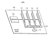
도 15를 참조하면, 컴퓨팅 시스템(600a)은 보드(670), 프로세서(610) 및 광 메모리 시스템을 포함한다. 상기 광 메모리 시스템은 광원(110), 광 분배부(200) 및 복수의 메모리 모듈들(131, 133, 135, 137)을 포함할 수 있다.Referring to FIG. 15, the
예를 들어, 보드(670)는 마더 모드(mother board) 또는 메인 보드(main board)일 수 있다. 프로세서(610)는 보드(670) 상에 장착되고, 상기 광 메모리 시스템을 제어하는 메모리 컨트롤러를 포함할 수 있다. 광 분배부(200)는 광원(110)에서 생성된 광을 복수의 메모리 모듈들(131, 133, 135, 137)에 분배할 수 있다. 복수의 메모리 모듈들(131, 133, 135, 137)은 광원(110)으로부터 광 분배부(200)를 통하여 수신된 광을 이용하여 광 신호를 생성하고, 상기 광 신호를 상기 메모리 컨트롤러에 제공할 수 있다.For example, the
도 15에 도시된 바와 같이, 광원(110)은 복수의 메모리 모듈들(131, 133, 135, 137)의 외부에 위치하고, 보드(670) 상에 장착될 수 있다. 또한, 복수의 메모리 모듈들(131, 133, 135, 137)은 보드(670) 상에 장착된 광원(110)을 공유할 수 있다.As shown in FIG. 15, the
도 16은 본 발명의 실시예들에 따른 광 메모리 시스템에 포함된 광원의 위치를 설명하기 위한 서버 시스템의 일 예를 나타내는 도면이다.16 is a diagram illustrating an example of a server system for describing a location of a light source included in an optical memory system according to example embodiments.
도 16을 참조하면, 서버 시스템(700)은 각각 복수의 컴퓨팅 시스템들(600)이 장착된 복수의 랙들(710, 720) 및 복수의 광원들(110)이 장착된 랙(730)을 포함할 수 있다.Referring to FIG. 16, the
각 광원(110)은 상응하는 컴퓨팅 시스템(600)의 보드의 외부에 위치하고, 랙 타입으로 구현될 수 있다. 랙(730)에 장착된 복수의 광원들(110)에서 생성된 광들(LT)이 복수의 랙들(710, 720)에 장착된 복수의 컴퓨팅 시스템들(600)에 각각 제공될 수 있다.Each
도 17은 본 발명의 다른 실시예들에 따른 광 메모리 시스템을 나타내는 블록도이다.17 is a block diagram illustrating an optical memory system according to example embodiments.
도 17을 참조하면, 광 메모리 시스템(1100)은 복수의 광원들(1111, 1113, 1115, 1117) 및 복수의 메모리 모듈들(1131, 1133, 1135, 1137)을 포함한다.Referring to FIG. 17, the
복수의 광원들(1111, 1113, 1115, 1117)은 복수의 광들(LT1, LT2, LT3, LT4)을 각각 생성할 수 있다. 또한, 복수의 광원들(1111, 1113, 1115, 1117)은 복수의 메모리 모듈들(1131, 1133, 1135, 1137)에 각각 연결되고, 복수의 광들(LT1, LT2, LT3, LT4)을 복수의 메모리 모듈들(1131, 1133, 1135, 1137)에 각각 제공할 수 있다. 예를 들어, 제1 광원(1111)은 제1 메모리 모듈(1131)에 연결되고, 제1 광(LT1)을 제1 메모리 모듈(1131)에 포함된 제1 전광 변환부(1132)에 제공할 수 있다. 또한, 제2 광원(1113)은 제2 메모리 모듈(1133)에 연결되고, 제2 광(LT2)을 제2 메모리 모듈(1133)에 포함된 제2 전광 변환부(1134)에 제공할 수 있다. 또한, 제3 광원(1115)은 제3 메모리 모듈(1135)에 연결되고, 제3 광(LT3)을 제3 메모리 모듈(1135)에 포함된 제3 전광 변환부(1136)에 제공할 수 있다. 또한, 제4 광원(1117)은 제4 메모리 모듈(1137)에 연결되고, 제4 광(LT4)을 제4 메모리 모듈(1137)에 포함된 제4 전광 변환부(1138)에 제공할 수 있다. 이와 같이, 광 메모리 시스템(1100)은 복수의 메모리 모듈들(1131, 1133, 2135, 1137)에 각각 상응하는 복수의 광원들(1111, 1113, 1115, 1117)을 포함할 수 있다.The plurality of
한편, 실시예에 따라, 복수의 전광 변환부들(1132, 1134, 1136, 1138) 각각은 도 8의 전광 변환부(300) 또는 도 9의 전광 변환부(400)와 같이 구현될 수 있다. 또한, 실시예에 따라, 각 광원(1111, 1113, 1115, 1117)은 상응하는 메모리 모듈 내에 위치하거나, 광 메모리 시스템(1100)이 장착된 보드 상에 장착되거나, 광 메모리 시스템(1100)이 장착된 보드의 외부에 위치할 수 있다.In some embodiments, each of the plurality of all-optical converting
도 18은 본 발명의 다른 실시예들에 따른 광 메모리 시스템에 포함된 광원의 위치를 설명하기 위한 메모리 모듈의 일 예를 나타내는 도면이다.FIG. 18 is a diagram illustrating an example of a memory module for describing a location of a light source included in an optical memory system according to example embodiments. FIG.
도 18을 참조하면, 메모리 모듈(1200)은 복수의 메모리 장치들(1230), 전광 변환부(1220) 및 광원(1210)을 포함할 수 있다. 일 실시예에서, 도 17의 각 메모리 모듈(1331, 1133, 1135, 1137)은 도 18의 메모리 모듈(2200)과 같이 구현될 수 있다.Referring to FIG. 18, the
광원(1210)은 광(LT)을 생성하고, 전광 변환부(1220)는 광원(1210)에서 생성된 광(LT)을 이용하여 복수의 메모리 장치들(1230)로부터 출력된 전기 신호를 광 신호(OS)로 변환할 수 있다. 도 18에 도시된 바와 같이, 광원(1210)은 상응하는 메모리 모듈(1200) 내에 위치할 수 있다.The
도 19는 본 발명의 다른 실시예들에 따른 광 메모리 시스템에 포함된 광원의 위치를 설명하기 위한 컴퓨팅 시스템의 일 예를 나타내는 도면이다.FIG. 19 is a diagram illustrating an example of a computing system for describing a location of a light source included in an optical memory system according to example embodiments.
도 19를 참조하면, 컴퓨팅 시스템(1300)은 보드(1370), 프로세서(1310) 및 광 메모리 시스템을 포함한다. 상기 광 메모리 시스템은 복수의 광원들(1111, 1113, 1115, 1117) 및 복수의 메모리 모듈들(1131, 1133, 1135, 1137)을 포함할 수 있다.Referring to FIG. 19, the
프로세서(1310)는 보드(1370) 상에 장착되고, 상기 광 메모리 시스템을 제어하는 메모리 컨트롤러를 포함할 수 있다. 각 광원(1111, 1113, 1115, 1117)은 상응하는 메모리 모듈(1131, 1133, 1135, 1137)에 연결되고, 상응하는 메모리 모듈(1131, 1133, 1135, 1137)에 광을 제공할 수 있다.The
일 실시예에서, 도 19에 도시된 바와 같이, 복수의 광원들(1111, 1113, 1115, 1117)은 복수의 메모리 모듈들(1131, 1133, 1135, 1137)의 외부에 위치하고, 보드(1370) 상에 장착될 수 있다. 다른 실시예에서, 도 16에 도시된 바와 같이, 복수의 광원들(1111, 1113, 1115, 1117)은 보드(1370)의 외부에 위치하고, 랙 타입으로 구현될 수 있다.In an embodiment, as shown in FIG. 19, the plurality of
도 20은 본 발명의 또 다른 실시예들에 따른 광 메모리 시스템을 나타내는 블록도이다.20 is a block diagram illustrating an optical memory system according to example embodiments of the inventive concepts.
도 20을 참조하면, 광 메모리 시스템(2100)은 제1 광원(2110), 제2 광원(2115), 복수의 메모리 모듈들(2131, 2133, 2135, 2137), 제1 광 분배부(2200) 및 제2 광 분배부(2250)를 포함한다.Referring to FIG. 20, the
제1 광원(2110)은 제1 광(LT1)을 생성하고, 제2 광원(2115)은 제2 광(LT2)을 생성할 수 있다. 제1 광 분배부(2200)는 제1 광원(2110)과 복수의 메모리 모듈들(2131, 2133, 2135, 2137) 사이에 연결되어 제1 광원(2110)에서 생성된 제1 광(LT1)을 복수의 메모리 모듈들(2131, 2133, 2135, 2137)에 분배하고, 제2 광 분배부(2250)는 제2 광원(2115)과 복수의 메모리 모듈들(2131, 2133, 2135, 2137) 사이에 연결되어 제2 광원(2115)에서 생성된 제2 광(LT2)을 복수의 메모리 모듈들(2131, 2133, 2135, 2137)에 분배할 수 있다. 실시예에 따라, 제1 및 제2 광 분배부들(2200, 2250) 각각은 복수의 메모리 모듈들(2131, 2133, 2135, 2137) 중 하나의 메모리 모듈에만 광을 제공하는 도 5의 광 분배부(200d), 도 6의 광 분배부(200e) 또는 도 7의 광 분배부(200f)와 같이 구현될 수 있다.The
제1 및 제2 광 분배부들(2200, 2250)은, 메모리 컨트롤러로부터 제공된 제어 신호에 응답하여 복수의 메모리 모듈들(2131, 2133, 2135, 2137) 중 현재 활성화된 메모리 모듈에 제1 광(LT1) 또는 제2 광(LT2) 중 하나를 제공하고, 복수의 메모리 모듈들(2131, 2133, 2135, 2137) 중 다음에 활성화될 메모리 모듈에 제1 광(LT1) 또는 제2 광(LT2) 중 다른 하나를 제공할 수 있다. 즉, 제1 및 제2 광 분배부들(2200, 2250)에 의해 제1 광(LT1) 또는 제2 광(LT2) 중 어느 하나가 상기 현재 활성화된 메모리 모듈에 제공되고, 제1 광(LT1) 또는 제2 광(LT2) 중 다른 하나가 상기 다음에 활성화될 메모리 모듈에 제공될 수 있다. 이에 따라, 광 분배부의 스위칭 속도가 메모리 모듈의 선택 속도보다 느리더라도 (또는 광 분배부의 스위칭 레이턴시가 메모리 모듈의 선택 레이턴시보다 길더라도), 활성화된 메모리 모듈에 광이 정확하게 제공될 수 있다.The first and second
예를 들어, 제2 메모리 모듈(2133)이 현재 활성화 상태이고 (또는 현재 독출 동작을 수행하고), 제4 메모리 모듈(2137)이 다음으로 활성화될 (또는 다음으로 독출 동작을 수행할) 경우, 제1 및 제2 광 분배부들(2200, 2250)은 상기 메모리 컨트롤러로부터 제2 메모리 모듈(2133)이 활성화 상태임을 나타내는 현재 칩 선택 신호(CCCS) 및 제4 메모리 모듈(2137)이 다음에 활성화됨을 나타내는 다음 칩 선택 신호(NCCS)를 수신할 수 있다. 제1 광 분배부(2200)는 제2 메모리 모듈(2133)을 나타내는 현재 칩 선택 신호(CCCS)에 응답하여 제1 광(LT1)을 제2 메모리 모듈(2133)에 제공하고, 제2 광 분배부(2250)는 제4 메모리 모듈(2137)을 나타내는 다음 칩 선택 신호(NCCS)에 응답하여 제2 광(LT2)을 제4 메모리 모듈(2137)에 미리 제공할 수 있다.For example, when the
이어서, 제2 메모리 모듈(2133)이 독출 동작을 완료한 후 제4 메모리 모듈(2137)이 현재 활성화되고, 제4 메모리 모듈(2137)의 다음으로 제1 메모리 모듈(2131)이 활성화될 경우, 제1 및 제2 광 분배부들(2200, 2250)은 상기 메모리 컨트롤러로부터 제4 메모리 모듈(2137)이 활성화 상태임을 나타내는 현재 칩 선택 신호(CCCS) 및 제1 메모리 모듈(2131)이 다음에 활성화됨을 나타내는 다음 칩 선택 신호(NCCS)를 수신할 수 있다. 제2 광 분배부(2250)는 제4 메모리 모듈(2137)을 나타내는 현재 칩 선택 신호(CCCS)에 응답하여 제2 광(LT2)을 제4 메모리 모듈(2137)에 계속하여 제공하고, 제1 광 분배부(2200)는 제1 메모리 모듈(2131)을 나타내는 다음 칩 선택 신호(NCCS)에 응답하여 제1 광(LT1)을 제1 메모리 모듈(2131)에 미리 제공할 수 있다.Subsequently, when the
복수의 메모리 모듈들(2131, 2133, 2135, 2137) 각각은 복수의 메모리 장치들을 구비하고, 제1 광(LT1) 또는 제2 광(LT2)을 이용하여 상기 복수의 메모리 장치들로부터 출력된 전기 신호를 광 신호(OS)로 변환함으로써 상기 메모리 컨트롤러에 광 신호(OS)를 출력할 수 있다. 각 메모리 모듈(2131, 2133, 2135, 2137)은 전광 변환부(2132, 2134, 2136, 2138)를 포함할 수 있다. 각 전광 변환부(2132, 2134, 2136, 2138)는 제1 광(LT1) 또는 제2 광(LT2) 중 하나의 광을 수신하고, 상기 복수의 메모리 장치들로부터 출력된 상기 전기 신호에 응답하여 상기 수신된 광을 변조함으로써 광 신호(OS)를 생성할 수 있다. 각 전광 변환부(2132, 2134, 2136, 2138)로부터 출력된 광 신호(OS)는 광 전송로를 통하여 상기 메모리 컨트롤러에 제공될 수 있다.Each of the plurality of
상술한 바와 같이, 본 발명의 또 다른 실시예들에 따른 광 메모리 시스템(2100)에서, 제1 광원(2110)에서 생성된 제1 광(LT1) 또는 제2 광원(2115)에서 생성된 제2 광(LT2) 중 어느 하나가 상기 현재 활성화된 메모리 모듈에 제공되고, 다른 하나가 상기 다음에 활성화될 메모리 모듈에 제공될 수 있다. 이에 따라, 광 분배부의 스위칭 속도가 느리더라도, 활성화된 메모리 모듈에 광이 정확하게 제공될 수 있다.As described above, in the
도 21은 본 발명의 또 다른 실시예들에 따른 메모리 모듈에 포함된 전광 변환부의 일 예를 나타내는 블록도이다.FIG. 21 is a block diagram illustrating an example of an all-optical converter included in a memory module according to example embodiments. FIG.
도 21을 참조하면, 전광 변환부(2300)는 광 결합기(2350), 광 스플리터(2310) 및 복수의 광 변조기들(2330)을 포함한다. 일 실시예에서, 도 20 에 도시된 각 메모리 모듈(2131, 2133, 2135, 2137)에 포함된 전광 변환부(2132, 2134, 2136, 2138)는 도 21의 전광 변환부(2300)와 같이 구현될 수 있다.Referring to FIG. 21, the all-optical converting
광 결합기(2350)는 제1 광 분배부를 통하여 제1 광원에서 생성된 제1 광(LT1)을 수신하고, 제2 광 분배부를 통하여 제2 광원에서 생성된 제2 광(LT2)을 수신할 수 있다. 광 결합기(2350)는 상기 제1 광원에서 생성된 제1 광(LT1) 및 상기 제2 광원에서 생성된 제2 광(LT2)을 결합하여 결합된 광을 생성하고, 상기 결합된 광을 광 스플리터(2310)에 제공할 수 있다. 이에 따라, 광 결합기(2350)가 광 스플리터(2310)에 제1 광(LT1) 및 제2 광(LT2)이 결합된 광을 제공하므로, 광 결합기(2350)에 상기 제1 광원에서 생성된 제1 광(LT1) 또는 상기 제2 광원에서 생성된 제2 광(LT2) 중 어느 하나의 광만이 제공되더라도, 광 스플리터(2310)에 제공되는 광은 원하는 광 세기를 가질 수 있다.The
광 스플리터(2310)는 광 결합기(2350)로부터 수신된 상기 결합된 광을 복수의 광들로 분할하고, 상기 복수의 광들을 복수의 광 변조기들(2330)에 각각 제공할 수 있다. 복수의 광 변조기들(2330)은 전광 변환부(2300)가 위치한 메모리 모듈에 포함된 메모리 장치들로부터 출력된 전기 신호들(SOUT)을 수신하고, 전기 신호들(SOUT)에 기초하여 상기 복수의 광들을 변조함으로써 복수의 광 신호들(OS)을 생성할 수 있다.The
도 22는 본 발명의 또 다른 실시예들에 따른 메모리 모듈에 포함된 전광 변환부의 다른 예를 나타내는 블록도이다.FIG. 22 is a block diagram illustrating another example of an all-optical converter included in a memory module according to example embodiments. FIG.
도 22를 참조하면, 전광 변환부(2400)는 광 결합기(2450), 직렬화기(2410) 및 광 변조기(2430)를 포함한다. 일 실시예에서, 도 20 에 도시된 각 메모리 모듈(2131, 2133, 2135, 2137)에 포함된 전광 변환부(2132, 2134, 2136, 2138)는 도 21의 전광 변환부(2400)와 같이 구현될 수 있다.Referring to FIG. 22, the all-
광 결합기(2450)는 제1 광 분배부를 통하여 제1 광원에서 생성된 제1 광(LT1)을 수신하고, 제2 광 분배부를 통하여 제2 광원에서 생성된 제2 광(LT2)을 수신할 수 있다. 광 결합기(2450)는 상기 제1 광원에서 생성된 제1 광(LT1) 및 상기 제2 광원에서 생성된 제2 광(LT2)을 결합하여 결합된 광을 생성하고, 상기 결합된 광을 광 변조기(2430)에 제공할 수 있다. 이에 따라, 광 결합기(2450)가 광 변조기(2430)에 제1 광(LT1) 및 제2 광(LT2)이 결합된 광을 제공하므로, 광 결합기(2450)에 상기 제1 광원에서 생성된 제1 광(LT1) 또는 상기 제2 광원에서 생성된 제2 광(LT2) 중 어느 하나의 광만이 제공되더라도, 광 변조기(2430)에 제공되는 광은 원하는 광 세기를 가질 수 있다.The
직렬화기(2410)는 전광 변환부(2300)가 위치한 메모리 모듈에 포함된 메모리 장치들로부터 출력된 전기 신호들(SOUT)을 직렬화하여 직렬화된 전기 신호를 광 변조기(2430)에 제공할 수 있다. 광 변조기(2430)는 직렬화기(2410)로부터 상기 직렬화된 전기 신호를 수신하고, 광 결합기(2450)로부터 상기 결합된 광을 수신할 수 있다. 광 변조기(2430)는 상기 직렬화된 전기 신호에 기초하여 상기 결합된 광을 변조함으로써 광 신호(OS)를 생성할 수 있다.The
도 23은 본 발명의 또 다른 실시예들에 따른 광 메모리 시스템을 나타내는 블록도이다.FIG. 23 is a block diagram illustrating an optical memory system according to example embodiments. Referring to FIG.
도 23을 참조하면, 광 메모리 시스템(1100)은 광원 모듈(3110), 복수의 메모리 모듈들(3131, 3133, 3135, 3137) 및 복수의 광 분배부들(3200, 3250)을 포함한다.Referring to FIG. 23, the
광원 모듈(3110)은 복수의 광원들(3111, 3113)을 포함한다. 복수의 광원들(3111, 3113)은 복수의 광들(LT1, LT2)을 각각 생성할 수 있다. 복수의 광 분배부들(3200, 3250) 각각은 복수의 광원들(3111, 3113) 중 상응하는 광원과 복수의 메모리 모듈들(3131, 3133, 3135, 3137) 사이에 연결되고, 상기 상응하는 광원에서 생성된 광을 복수의 메모리 모듈들(3131, 3133, 3135, 3137)에 분배할 수 있다. 예를 들어, 광원 모듈(3110)은 제1 광원(3111) 및 제2 광원(3113)을 포함하고, 복수의 광 분배부들(3200, 3250)은 제1 광 분배부(3200) 및 제2 광 분배부(3250)를 포함하며, 제1 광 분배부(3200)는 제1 광원(3111)과 복수의 메모리 모듈들(3131, 3133, 3135, 3137) 사이에 연결되어 제1 광원(3111)에서 생성된 제1 광(LT1)을 복수의 메모리 모듈들(3131, 3133, 3135, 3137)에 분배하고, 제2 광 분배부(3250)는 제2 광원(3113)과 복수의 메모리 모듈들(3131, 3133, 3135, 3137) 사이에 연결되어 제2 광원(3113)에서 생성된 제2 광(LT2)을 복수의 메모리 모듈들(3131, 3133, 3135, 3137)에 분배할 수 있다. 실시예에 따라, 복수의 광 분배부들(3200, 3250) 각각은 복수의 메모리 모듈들(3131, 3133, 3135, 3137) 중 하나의 메모리 모듈에만 광(LT1, LT2)을 제공하는 도 5의 광 분배부(200d), 도 6의 광 분배부(200e) 또는 도 7의 광 분배부(200f)와 같이 구현될 수 있다.The
각 메모리 모듈(3131, 3133, 3135, 3137)은 복수의 메모리 장치들을 구비하고, 복수의 광원들(3111, 3113)에서 생성된 복수의 광들(LT1, LT2)을 이용하여 상기 복수의 메모리 장치들로부터 출력된 전기 신호를 광 신호(OS)로 변환함으로써 메모리 컨트롤러에 광 신호(OS)를 출력할 수 있다. 각 메모리 모듈(3131, 3133, 3135, 3137)은 전광 변환부(3132, 3134, 3136, 3138)를 포함할 수 있다. 각 전광 변환부(3132, 3134, 3136, 3138)는 복수의 광원들(3111, 3113)로부터 복수의 광 분배부들(3200, 3250)을 통하여 복수의 광들(LT1, LT2)을 수신하고, 상기 복수의 메모리 장치들로부터 출력된 상기 전기 신호에 응답하여 수신된 복수의 광들(LT1, LT2)을 변조함으로써 광 신호(OS)를 생성할 수 있다. 각 전광 변환부(3132, 3134, 3136, 3138)로부터 출력된 광 신호(OS)는 광 전송로를 통하여 상기 메모리 컨트롤러에 제공될 수 있다.Each of the
일 실시예에서, 각 메모리 모듈(3131, 3133, 3135, 3137)에 포함된 상기 복수의 메모리 장치들이 복수의 메모리 장치 그룹들로 그룹화되고, 복수의 광원들(3111, 3113)로부터 생성된 복수의 광들(LT1, LT2)은 상기 복수의 메모리 장치 그룹들로부터 각각 출력된 복수의 전기 신호들을 복수의 광 신호들로 변환하는 데에 각각 이용될 수 있다. 예를 들어, 각 메모리 모듈(3131, 3133, 3135, 3137)은 상기 복수의 메모리 장치들 중 일부를 포함하는 제1 메모리 장치 그룹 및 상기 복수의 메모리 장치들 중 다른 일부를 포함하는 제2 메모리 장치 그룹을 포함할 수 있고, 제1 광원(3111)에서 생성된 제1 광(LT1)은 상기 제1 메모리 장치 그룹으로부터 출력된 제1 전기 신호를 제1 광 신호로 변환하는 데에 이용되고, 제2 광원(3113)에서 생성된 제2 광(LT2)은 상기 제2 메모리 장치 그룹으로부터 출력된 제2 전기 신호를 제2 광 신호로 변환하는 데에 이용될 수 있다. 즉, 본 발명의 다른 실시예들에 따른 광 메모리 시스템(3100)은 하나의 메모리 모듈에 포함된 메모리 장치 그룹들의 수만큼의 광원들(3111, 3113)을 포함할 수 있고, 각 광원(3111, 3113)은 복수의 메모리 모듈들(3131, 3133, 3135, 3137)에 각각 포함된 상응하는 메모리 장치 그룹들에 의해 공유될 수 있다. 한편, 각 메모리 모듈(3131, 3133, 3135, 3137)은 적어도 하나의 랭크(rank)를 포함할 수 있고, 상기 랭크는 각각이 적어도 하나의 메모리 장치를 포함하는 복수의 서브-랭크들로 구분될 수 있으며, 상기 복수의 메모리 장치 그룹들은 상기 복수의 서브-랭크들에 상응할 수 있다. 즉, 광 메모리 시스템(3100)은 하나의 랭크 포함된 서브-랭크들의 수만큼의 광원들(3111, 3113)을 포함할 수 있고, 각 광원(3111, 3113)은 복수의 메모리 모듈들(3131, 3133, 3135, 3137)에 각각 포함된 상응하는 서브-랭크들에 의해 공유될 수 있다.In one embodiment, the plurality of memory devices included in each of the
상술한 바와 같이, 본 발명의 또 다른 실시예들에 따른 광 메모리 시스템(3100)에서, 복수의 광원들(3111, 3113)에서 생성된 복수의 광들(LT1, LT2)이 광 분배부(3200)에 의해 복수의 메모리 모듈들(3131, 3133, 3135, 3137)에 분배됨으로써, 복수의 메모리 모듈들(3131, 3133, 3135, 3137)은 복수의 광원(3111, 3113)을 공유할 수 있다. 이에 따라, 본 발명의 다른 실시예들에 따른 광 메모리 시스템(3100)은, 각 메모리 모듈 마다 하나 이상의 광원을 포함하는 종래의 광 메모리 시스템에 비하여, 적은 수의 광원을 포함할 수 있고, 광 메모리 시스템(3100)의 비용 및 전력 소모를 감소시킬 수 있다.As described above, in the
도 24는 도 23의 광 메모리 시스템에 포함된 메모리 모듈의 일 예를 나타내는 블록도이다.FIG. 24 is a block diagram illustrating an example of a memory module included in the optical memory system of FIG. 23.
도 24를 참조하면, 메모리 모듈(3300)은 제1 내지 제4 메모리 장치들(3311, 3313, 3315, 3317)을 포함하는 제1 메모리 장치 그룹(3310), 제5 내지 제8 메모리 장치들(3321, 3323, 3325, 3327)을 포함하는 제2 메모리 장치 그룹(3320) 및 전광 변환부(3330)를 포함할 수 있다. 일 실시예에서, 도 23의 각 메모리 모듈(3331, 3133, 3135, 3137)은 도 24의 메모리 모듈(3300)과 같이 구현될 수 있다.Referring to FIG. 24, the
전광 변환부(3330)는 제1 메모리 장치 그룹(3310)으로부터 제1 전기 신호(SOUT1)를 수신하고, 제2 메모리 장치 그룹(3320)으로부터 제2 전기 신호(SOUT2)를 수신하며, 도 23의 제1 광원(3111)으로부터 제1 광 분배부(3200)를 통하여 제1 광(LT1)을 수신하고, 도 23의 제2 광원(3113)으로부터 제2 광 분배부(3250)를 통하여 제2 광(LT2)을 수신할 수 있다. 전광 변환부(3330)는 제1 메모리 장치 그룹(3310)으로부터 출력된 제1 전기 신호(SOUT1)에 기초하여 제1 광(LT1)을 변조함으로써 제1 전기 신호(SOUT1)에 상응하는 제1 광 신호(OS1)를 생성하고, 제2 메모리 장치 그룹(3320)으로부터 출력된 제2 전기 신호(SOUT2)에 기초하여 제2 광(LT2)을 변조함으로써 제2 전기 신호(SOUT2)에 상응하는 제2 광 신호(OS2)를 생성할 수 있다. 이와 같이, 도 23의 제1 광원(3111)에서 생성된 제1 광(LT1)은 제1 메모리 장치 그룹(3310)으로부터 출력된 제1 전기 신호(SOUT1)를 제1 광 신호(OS1)로 변환하는 데에 이용되고, 도 23의 제2 광원(3113)에서 생성된 제2 광(LT2)은 제2 메모리 장치 그룹(3320)으로부터 출력된 제2 전기 신호(SOUT2)를 제2 광 신호(OS2)로 변환하는 데에 이용될 수 있다. 한편, 복수의 메모리 장치 그룹들(3310, 3320)은 하나의 랭크에 포함된 복수의 서브-랭크들에 상응하고, 광 메모리 시스템은 하나의 랭크 포함된 서브-랭크들의 수만큼의 광원들을 포함하며, 각 광원은 복수의 메모리 모듈들에 각각 포함된 상응하는 서브-랭크들에 의해 공유될 수 있다.The all-
한편, 도 24에는 각 메모리 모듈(3300)이 두 개의 메모리 장치 그룹들(3310, 3320)을 포함하는 예가 도시되어 있으나, 실시예에 따라, 각 메모리 모듈(3300)은 세 개 이상의 메모리 장치 그룹들을 포함할 수 있다. 이 경우, 도 23의 광원 모듈(3110)은 세 개 이상의 광원들을 포함할 수 있다.Meanwhile, although FIG. 24 illustrates an example in which each
도 25는 본 발명의 또 다른 실시예들에 따른 메모리 모듈에 포함된 전광 변환부의 일 예를 나타내는 블록도이다.FIG. 25 is a block diagram illustrating an example of an all-optical converter included in a memory module according to example embodiments. FIG.
도 25를 참조하면, 전광 변환부(3330a)는 제1 광 스플리터(3331a), 제1 광 변조부(3333a), 제2 광 스플리터(3332a) 및 제2 광 변조부(3335a)를 포함한다. 제1 광 변조부(3333a)는 복수의 제1 광 변조기들(3334a)을 포함하고, 제2 광 변조부(3335a)는 복수의 제2 광 변조기들(3336a)을 포함할 수 있다. 일 실시예에서, 도 23 및 도 24에 도시된 각 메모리 모듈(3131, 3133, 3135, 3137, 3300)에 포함된 전광 변환부(3132, 3134, 3136, 3138, 3300)는 도 25의 전광 변환부(3330a)와 같이 구현될 수 있다.Referring to FIG. 25, the all-
제1 광 스플리터(3331a)는 도 23의 제1 광원(3111)으로부터 제1 광 분배부(3200)를 통하여 수신된 제1 광(LT1)을 복수의 제1 광들로 분할하여 상기 복수의 제1 광들을 제1 광 변조부(3333a)에 포함된 복수의 제1 광 변조기들(3334a)에 각각 제공할 수 있다. 복수의 제1 광 변조기들(3334a)은 도 24의 제1 메모리 장치 그룹(3310)으로부터 출력된 제1 전기 신호들(SOUT1)을 수신하고, 제1 전기 신호들(SOUT1)에 기초하여 상기 복수의 제1 광들을 변조함으로써 복수의 제1 광 신호들(OS1)을 생성할 수 있다. 복수의 제1 광 변조기들(3334a)은 복수의 제1 광 신호들(OS1)을 메모리 컨트롤러에 제공할 수 있다.The first
또한, 제2 광 스플리터(3332a)는 도 23의 제2 광원(3113)으로부터 제2 광 분배부(3250)를 통하여 수신된 제2 광(LT2)을 복수의 제2 광들로 분할하여 상기 복수의 제2 광들을 제2 광 변조부(3335a)에 포함된 복수의 제2 광 변조기들(3336a)에 각각 제공할 수 있다. 복수의 제2 광 변조기들(3336a)은 도 24의 제2 메모리 장치 그룹(3320)으로부터 출력된 제2 전기 신호들(SOUT2)을 수신하고, 제2 전기 신호들(SOUT2)에 기초하여 상기 복수의 제2 광들을 변조함으로써 복수의 제2 광 신호들(OS2)을 생성할 수 있다. 복수의 제2 광 변조기들(3336a)은 복수의 제2 광 신호들(OS2)을 상기 메모리 컨트롤러에 제공할 수 있다.In addition, the second
도 26은 본 발명의 또 다른 실시예들에 따른 메모리 모듈에 포함된 전광 변환부의 다른 예를 나타내는 블록도이다.FIG. 26 is a block diagram illustrating another example of an all-optical converter included in a memory module according to example embodiments. FIG.
도 26을 참조하면, 전광 변환부(3330b)는 제1 직렬화기(3337b), 제1 광 변조기(3333b), 제2 직렬화기(3339b) 및 제2 광 변조기(3335b)를 포함한다. 일 실시예에서, 도 23 및 도 24에 도시된 각 메모리 모듈(3131, 3133, 3135, 3137, 3300)에 포함된 전광 변환부(3132, 3134, 3136, 3138, 3300)는 도 26의 전광 변환부(3330b)와 같이 구현될 수 있다.Referring to FIG. 26, the all-
제1 직렬화기(3337b)는 도 24의 제1 메모리 장치 그룹(3310)으로부터 출력된 제1 전기 신호들(SOUT1)을 직렬화하여 제1 직렬화된 전기 신호를 제1 광 변조기(3333b)에 제공할 수 있다. 제1 광 변조기(3333b)는 제1 직렬화기(3337b)로부터 상기 제1 직렬화된 전기 신호를 수신하고, 도 23의 제1 광원(3111)으로부터 제1 광 분배부(3200)를 통하여 제1 광(LT1)을 수신할 수 있다. 제1 광 변조기(3333b)는 상기 제1 직렬화된 전기 신호에 기초하여 제1 광(LT1)을 변조함으로써 제1 광 신호(OS1)를 생성할 수 있다. 제1 광 변조기(3333b)는 제1 광 신호(OS1)를 메모리 컨트롤러에 제공할 수 있다.The
또한, 제2 직렬화기(3339b)는 도 24의 제2 메모리 장치 그룹(3320)으로부터 출력된 제2 전기 신호들(SOUT2)을 직렬화하여 제2 직렬화된 전기 신호를 제2 광 변조기(3335b)에 제공할 수 있다. 제2 광 변조기(3335b)는 제2 직렬화기(3339b)로부터 상기 제2 직렬화된 전기 신호를 수신하고, 도 23의 제2 광원(3113)으로부터 제2 광 분배부(3250)를 통하여 제2 광(LT2)을 수신할 수 있다. 제2 광 변조기(3335b)는 상기 제2 직렬화된 전기 신호에 기초하여 제2 광(LT2)을 변조함으로써 제2 광 신호(OS2)를 생성할 수 있다. 제2 광 변조기(3335b)는 제2 광 신호(OS2)를 상기 메모리 컨트롤러에 제공할 수 있다.In addition, the
도 27은 본 발명의 또 다른 실시예들에 따른 광 메모리 시스템을 나타내는 블록도이다.FIG. 27 is a block diagram illustrating an optical memory system according to example embodiments. FIG.
도 27을 참조하면, 광 메모리 시스템(4100)은 복수의 광원 모듈들(4110, 4115, 4120, 4125) 및 복수의 메모리 모듈들(4131, 4133, 4135, 4137)을 포함한다.Referring to FIG. 27, the
복수의 광원 모듈들(4110, 4115, 4120, 4125)은 복수의 메모리 모듈들(4131, 4133, 4135, 4137)에 각각 연결되고, 각 광원 모듈(4110, 4115, 4120, 4125)은 각 광원 모듈(4110, 4115, 4120, 4125)에 연결된 메모리 모듈에 복수의 광들을 제공할 수 있다. 또한, 각 광원 모듈(4110, 4115, 4120, 4125)은 하나의 메모리 모듈에 포함된 메모리 장치 그룹들의 수만큼 광원들(4111, 4113, 4116, 4118, 4121, 4123, 4126, 4128)을 포함할 수 있다. 예를 들어, 각 메모리 모듈(4131, 4133, 4135, 4137)이 2개의 메모리 장치 그룹들을 포함하는 경우, 각 광원 모듈(4110, 4115, 4120, 4125)은 2 개의 광들을 각각 생성하는 2 개의 광원들(4111, 4113, 4116, 4118, 4121, 4123, 4126, 4128)을 포함할 수 있다.The plurality of
예를 들어, 제1 메모리 모듈(4131)이 제1 메모리 장치 그룹 및 제2 메모리 장치 그룹을 포함하고, 제1 광원 모듈(4110)이 제1 광원(4111) 및 제2 광원(4113)을 포함할 수 있다. 제1 광원 모듈(4110)은 제1 메모리 모듈(4131)에 포함된 제1 전광 변환부(4132)에 제1 광원(4111)에서 생성된 제1 광(LT11) 및 제2 광원(4113)에서 생성된 제2 광(LT12)을 제공할 수 있다. 제1 전광 변환부(4132)는 제1 광(LT11)을 이용하여 상기 제1 메모리 장치 그룹으로부터 출력된 제1 전기 신호를 제1 광 신호로 변환하고, 제2 광(LT12)을 이용하여 상기 제2 메모리 장치 그룹으로부터 출력된 제2 전기 신호를 제2 광 신호로 변환할 수 있다. 이와 유사하게, 제2 메모리 모듈(4133)에 포함된 제2 전광 변환부(4134)는 제2 광원 모듈(4115)에 포함된 제3 광원(4116)으로부터 수신된 제3 광(LT21)을 이용하여 제3 메모리 장치 그룹으로 출력된 제3 전기 신호를 제3 광 신호로 변환하고, 제2 광원 모듈(4115)에 포함된 제4 광원(4118)으로부터 수신된 제4 광(LT22)을 이용하여 제4 메모리 장치 그룹으로 출력된 제4 전기 신호를 제4 광 신호로 변환할 수 있다. 또한, 제3 메모리 모듈(4135)에 포함된 제3 전광 변환부(4136)는 제3 광원 모듈(4120)에 포함된 제5 광원(4121)으로부터 수신된 제5 광(LT31)을 이용하여 제5 메모리 장치 그룹으로 출력된 제5 전기 신호를 제5 광 신호로 변환하고, 제3 광원 모듈(4120)에 포함된 제6 광원(4123)으로부터 수신된 제6 광(LT32)을 이용하여 제6 메모리 장치 그룹으로 출력된 제6 전기 신호를 제6 광 신호로 변환할 수 있다. 또한, 제4 메모리 모듈(4137)에 포함된 제4 전광 변환부(4138)는 제4 광원 모듈(4125)에 포함된 제7 광원(4126)으로부터 수신된 제7 광(LT41)을 이용하여 제7 메모리 장치 그룹으로 출력된 제7 전기 신호를 제7 광 신호로 변환하고, 제4 광원 모듈(4125)에 포함된 제8 광원(4128)으로부터 수신된 제8 광(LT42)을 이용하여 제8 메모리 장치 그룹으로 출력된 제8 전기 신호를 제8 광 신호로 변환할 수 있다. 이와 같이, 광 메모리 시스템(4100)은 각 메모리 모듈마다 복수의 광원들을 가지는 광원 모듈을 포함할 수 있다. 이에 따라, 각 메모리 모듈이 복수의 광원들로부터 광을 수신하므로, 각 메모리 모듈에 충분한 광 세기의 광이 제공될 수 있다.For example, the
한편, 실시예에 따라, 복수의 전광 변환부들(4132, 4134, 4136, 4138) 각각은 도 25의 전광 변환부(3300a) 또는 도 26의 전광 변환부(3300b)와 같이 구현될 수 있다. 또한, 실시예에 따라, 각 광원 모듈(4110, 4115, 4120, 4125)은 상응하는 메모리 모듈 내에 위치하거나, 광 메모리 시스템(4100)이 장착된 보드 상에 장착되거나, 광 메모리 시스템(4100)이 장착된 보드의 외부에 위치할 수 있다.In some embodiments, each of the plurality of all-
도 28은 본 발명의 또 다른 실시예들에 따른 광 메모리 시스템을 나타내는 블록도이다.FIG. 28 is a block diagram illustrating an optical memory system according to example embodiments. Referring to FIG.
도 28을 참조하면, 광 메모리 시스템(5100)은 제1 광원 모듈(5110), 제2 광원 모듈(5120), 복수의 메모리 모듈들(5131, 5133, 5135, 5137), 복수의 제1 광 분배부들(5200, 5210) 및 복수의 제2 광 분배부들(5250, 5260)을 포함한다.Referring to FIG. 28, the
제1 광원 모듈(5110)은 복수의 제1 광들(LT11, LT12)을 생성하는 복수의 제1 광원들(5111, 5113)을 포함하고, 제2 광원 모듈(5120)은 복수의 제2 광들(LT21, LT22)을 생성하는 복수의 제2 광원들(5121, 5123)을 포함할 수 있다. 일 실시예에서, 각 광원 모듈(5110, 5120)은 하나의 메모리 모듈에 포함된 메모리 장치 그룹들의 수만큼의 광원들을 포함할 수 있다. 복수의 제1 광 분배부들(5200, 5210)은 제1 광원 모듈(5110)과 복수의 메모리 모듈들(5131, 5133, 5135, 5137) 사이에 연결되어 제1 광원 모듈(5110)에서 생성된 복수의 제1 광들(LT11, LT12)을 복수의 메모리 모듈들(5131, 5133, 5135, 5137)에 분배하고, 복수의 제2 광 분배부들(5250, 5260)은 제2 광원 모듈(5120)과 복수의 메모리 모듈들(5131, 5133, 5135, 5137) 사이에 연결되어 제2 광원 모듈(5120)에서 생성된 복수의 제2 광들(LT21, LT22)을 복수의 메모리 모듈들(5131, 5133, 5135, 5137)에 분배할 수 있다. 실시예에 따라, 각 광 분배부(5200, 5210, 5250, 5260)는 복수의 메모리 모듈들(5131, 5133, 5135, 5137) 중 하나의 메모리 모듈에만 광을 제공하는 도 5의 광 분배부(200d), 도 6의 광 분배부(200e) 또는 도 7의 광 분배부(200f)와 같이 구현될 수 있다.The first
복수의 제1 광 분배부들(5200, 5210) 및 복수의 제2 광 분배부들(5250, 5260)은, 메모리 컨트롤러로부터 제공된 제어 신호에 응답하여 복수의 메모리 모듈들(5131, 5133, 5135, 5137) 중 현재 활성화된 메모리 모듈에 복수의 제1 광들(LT11, LT12) 또는 복수의 제2 광들(LT21, LT22)을 제공하고, 복수의 메모리 모듈들(5131, 5133, 5135, 5137) 중 다음에 활성화될 메모리 모듈에 복수의 제1 광들(LT11, LT12) 또는 복수의 제2 광들(LT21, LT22)을 제공할 수 있다. 즉, 복수의 제1 광 분배부들(5200, 5210) 및 복수의 제2 광 분배부들(5250, 5260)에 의해 복수의 제1 광들(LT11, LT12) 및 복수의 제2 광들(LT21, LT22)이 상기 현재 활성화된 메모리 모듈 및 상기 다음에 활성화될 메모리 모듈에 제공될 수 있다. 이에 따라, 광 분배부의 스위칭 속도가 메모리 모듈의 선택 속도보다 느리더라도 (또는 광 분배부의 스위칭 레이턴시가 메모리 모듈의 선택 레이턴시보다 길더라도), 활성화된 메모리 모듈에 복수의 광들이 정확하게 제공될 수 있다.The plurality of first
예를 들어, 제2 메모리 모듈(5133)이 현재 활성화 상태이고 (또는 현재 독출 동작을 수행하고), 제4 메모리 모듈(5137)이 다음으로 활성화될 (또는 다음으로 독출 동작을 수행할) 경우, 복수의 제1 광 분배부들(5200, 5210) 및 복수의 제2 광 분배부들(5250, 5260)은 상기 메모리 컨트롤러로부터 제2 메모리 모듈(5133)이 활성화 상태임을 나타내는 현재 칩 선택 신호(CCCS) 및 제4 메모리 모듈(5137)이 다음에 활성화됨을 나타내는 다음 칩 선택 신호(NCCS)를 수신할 수 있다. 복수의 제1 광 분배부들(5200, 5210)은 제2 메모리 모듈(5133)을 나타내는 현재 칩 선택 신호(CCCS)에 응답하여 복수의 제1 광들(LT11, LT12)을 제2 메모리 모듈(5133)에 제공할 수 있다. 제2 메모리 모듈(5133)은 복수의 메모리 장치 그룹들로부터의 전기 신호들을 복수의 제1 광들(LT11, LT12)을 각각 이용하여 광 신호들로 변환할 수 있다. 또한, 복수의 제2 광 분배부들(5250, 5260)은 제4 메모리 모듈(5137)을 나타내는 다음 칩 선택 신호(NCCS)에 응답하여 복수의 제2 광들(LT21, LT22)을 제4 메모리 모듈(5137)에 미리 제공할 수 있다.For example, when the
이어서, 제2 메모리 모듈(5133)이 독출 동작을 완료한 후 제4 메모리 모듈(5137)이 현재 활성화되고, 제5 메모리 모듈(5137)의 다음으로 제1 메모리 모듈(5131)이 활성화될 경우, 복수의 제1 광 분배부들(5200, 5210) 및 복수의 제2 광 분배부들(5250, 5260)은 상기 메모리 컨트롤러로부터 제4 메모리 모듈(5137)이 활성화 상태임을 나타내는 현재 칩 선택 신호(CCCS) 및 제1 메모리 모듈(5131)이 다음에 활성화됨을 나타내는 다음 칩 선택 신호(NCCS)를 수신할 수 있다. 복수의 제2 광 분배부들(5250, 5260)은 제4 메모리 모듈(5137)을 나타내는 현재 칩 선택 신호(CCCS)에 응답하여 복수의 제2 광들(LT21, LT22)을 제4 메모리 모듈(5137)에 계속하여 제공하고, 복수의 제1 광 분배부들(5200, 5210)은 제1 메모리 모듈(5131)을 나타내는 다음 칩 선택 신호(NCCS)에 응답하여 복수의 제1 광들(LT11, LT12)을 제1 메모리 모듈(5131)에 미리 제공할 수 있다.Subsequently, after the
복수의 메모리 모듈들(5131, 5133, 5135, 5137) 각각은 복수의 메모리 장치 그룹들을 구비하고, 복수의 제1 광들(LT11, LT12) 또는 복수의 제2 광들(LT21, LT22)을 이용하여 상기 복수의 메모리 장치 그룹들로부터 출력된 전기 신호를 광 신호(OS)로 변환함으로써 상기 메모리 컨트롤러에 광 신호(OS)를 출력할 수 있다. 각 메모리 모듈(5131, 5133, 5135, 5137)은 전광 변환부(5132, 5134, 5136, 5138)를 포함할 수 있다. 각 전광 변환부(5132, 5134, 5136, 5138)는 복수의 제1 광들(LT11, LT12) 또는 복수의 제2 광들(LT21, LT22)을 수신하고, 상기 복수의 메모리 장치 그룹들로부터 출력된 상기 전기 신호에 응답하여 상기 수신된 광들을 변조함으로써 광 신호(OS)를 생성할 수 있다. 각 전광 변환부(5132, 5134, 5136, 5138)로부터 출력된 광 신호(OS)는 광 전송로를 통하여 상기 메모리 컨트롤러에 제공될 수 있다.Each of the plurality of
상술한 바와 같이, 본 발명의 또 다른 실시예들에 따른 광 메모리 시스템(5100)에서, 복수의 제1 광들(LT11, LT12) 및 복수의 제2 광들(LT21, LT22)이 상기 현재 활성화된 메모리 모듈 및 상기 다음에 활성화될 메모리 모듈에 제공될 수 있다. 이에 따라, 광 분배부의 스위칭 속도가 느리더라도, 활성화된 메모리 모듈에 복수의 광들이 정확하게 제공될 수 있다.As described above, in the
한편, 도 28에는 각 광원 모듈(5110, 5120)이 두 개의 광원들을 포함하는 예가 도시되어 있으나, 실시예에 따라, 각 메모리 모듈(5132, 5134, 5136, 5138)은 세 개 이상의 메모리 장치 그룹들을 포함할 수 있고, 각 광원 모듈(5110, 5120)은 세 개 이상의 광원들을 포함할 수 있다.28 illustrates an example in which each
도 29는 본 발명의 또 다른 실시예들에 따른 메모리 모듈에 포함된 전광 변환부의 일 예를 나타내는 블록도이다.FIG. 29 is a block diagram illustrating an example of an all-optical converter included in a memory module according to example embodiments. FIG.
도 29를 참조하면, 전광 변환부(5330a)는 제1 광 결합기(5337a), 제1 광 스플리터(5331a), 제1 광 변조부(5333a), 제2 광 결합기(5338a), 제2 광 스플리터(5332a) 및 제2 광 변조부(5335a)를 포함한다. 제1 광 변조부(5333a)는 복수의 제1 광 변조기들(5334a)을 포함하고, 제2 광 변조부(5335a)는 복수의 제2 광 변조기들(5336a)을 포함할 수 있다. 일 실시예에서, 도 28에 도시된 각 메모리 모듈(5131, 5133, 5135, 5137)에 포함된 전광 변환부(5132, 5134, 5136, 5138)는 도 29의 전광 변환부(5330a)와 같이 구현될 수 있다.Referring to FIG. 29, the all-optical converting
도 28 및 도 29를 참조하면, 제1 광 결합기(5337a)는 제1 광 분배기(5200)를 통하여 제1 광원 모듈(5110)에 포함된 제1 광원(5111)에서 생성된 제1 광(LT11)을 수신하고, 제3 광 분배기(5250)를 통하여 제2 광원 모듈(5120)에 포함된 제3 광원(5121)에서 생성된 제3 광(LT21)을 수신할 수 있다. 제1 광 결합기(5337a)는 제1 광(LT11) 및 제3 광(LT21)을 결합하여 제1 결합된 광을 생성하고, 상기 제1 결합된 광을 제1 광 스플리터(5331a)에 제공할 수 있다. 이에 따라, 제1 광 결합기(5337a)가 제1 광 스플리터(5331a)에 제1 광(LT11) 및 제3 광(LT21)이 결합된 광을 제공하므로, 제1 광 결합기(5337a)에 제1 광(LT11) 또는 제3 광(LT21)중 어느 하나의 광만이 제공되더라도, 제1 광 스플리터(5331a)에 제공되는 광은 원하는 광 세기를 가질 수 있다.Referring to FIGS. 28 and 29, the
제1 광 스플리터(5331a)는 제1 광 결합기(5337a)으로부터 수신된 상기 제1 결합된 광을 복수의 광들로 분할하여 상기 복수의 광들을 제1 광 변조부(5333a)에 포함된 복수의 제1 광 변조기들(5334a)에 각각 제공할 수 있다. 복수의 제1 광 변조기들(5334a)은 제1 메모리 장치 그룹으로부터 출력된 제1 전기 신호들(SOUT1)을 수신하고, 제1 전기 신호들(SOUT1)에 기초하여 상기 복수의 광들을 변조함으로써 복수의 제1 광 신호들(OS1)을 생성할 수 있다. 복수의 제1 광 변조기들(5334a)은 복수의 제1 광 신호들(OS1)을 메모리 컨트롤러에 제공할 수 있다.The first
또한, 제2 광 결합기(5338a)는 제2 광 분배기(5210)를 통하여 제1 광원 모듈(5110)에 포함된 제2 광원(5113)에서 생성된 제2 광(LT12)을 수신하고, 제4 광 분배기(5260)를 통하여 제2 광원 모듈(5120)에 포함된 제4 광원(5123)에서 생성된 제4 광(LT22)을 수신할 수 있다. 제2 광 결합기(5338a)는 제2 광(LT12) 및 제4 광(LT22)을 결합하여 제2 결합된 광을 생성하고, 상기 제2 결합된 광을 제2 광 스플리터(5332a)에 제공할 수 있다. 이에 따라, 제2 광 결합기(5338a)가 제2 광 스플리터(5332a)에 제2 광(LT12) 및 제4 광(LT22)이 결합된 광을 제공하므로, 제2 광 결합기(5338a)에 제2 광(LT12) 또는 제4 광(LT22)중 어느 하나의 광만이 제공되더라도, 제2 광 스플리터(5332a)에 제공되는 광은 원하는 광 세기를 가질 수 있다.In addition, the second
제2 광 스플리터(5332a)는 제2 광 결합기(5338a)로부터 수신된 상기 제2 결합된 광을 복수의 광들로 분할하여 상기 복수의 광들을 제2 광 변조부(5335a)에 포함된 복수의 제2 광 변조기들(5336a)에 각각 제공할 수 있다. 복수의 제2 광 변조기들(5336a)은 제2 메모리 장치 그룹으로부터 출력된 제2 전기 신호들(SOUT2)을 수신하고, 제2 전기 신호들(SOUT2)에 기초하여 상기 복수의 광들을 변조함으로써 복수의 제2 광 신호들(OS2)을 생성할 수 있다. 복수의 제2 광 변조기들(5336a)은 복수의 제2 광 신호들(OS2)을 상기 메모리 컨트롤러에 제공할 수 있다.The second
이와 같이, 전광 변환부(5330a)는 제1 광원 모듈(5110)에서 생성된 광들(LT11, LT12)을 이용하여 상기 제1 및 제2 메모리 장치 그룹들로부터의 제1 및 제2 전기 신호들(SOUT1, SOUT2)를 제1 및 제2 광 신호들(OS1, OS2)로 변환하거나, 제2 광원 모듈(5120)에서 생성된 광들(LT21, LT22)을 이용하여 상기 제1 및 제2 메모리 장치 그룹들로부터의 제1 및 제2 전기 신호들(SOUT1, SOUT2)를 제1 및 제2 광 신호들(OS1, OS2)로 변환할 수 있다.As described above, the all-
도 30은 본 발명의 또 다른 실시예들에 따른 메모리 모듈에 포함된 전광 변환부의 다른 예를 나타내는 블록도이다.FIG. 30 is a block diagram illustrating another example of an all-optical converter included in a memory module according to example embodiments. FIG.
도 30을 참조하면, 전광 변환부(5330b)는 제1 광 결합기(5337b), 제1 직렬화기(5331b), 제1 광 변조기(5332b), 제2 광 결합기(5338b), 제2 직렬화기(5333b) 및 제2 광 변조기(5334b)를 포함한다. 일 실시예에서, 도 28에 도시된 각 메모리 모듈(5131, 5133, 5135, 5137)에 포함된 전광 변환부(5132, 5134, 5136, 5138)는 도 30의 전광 변환부(5330b)와 같이 구현될 수 있다.Referring to FIG. 30, the all-
도 28 및 도 30을 참조하면, 제1 광 결합기(5337b)는 제1 광 분배기(5200)를 통하여 제1 광원 모듈(5110)에 포함된 제1 광원(5111)에서 생성된 제1 광(LT11)을 수신하고, 제3 광 분배기(5250)를 통하여 제2 광원 모듈(5120)에 포함된 제3 광원(5121)에서 생성된 제3 광(LT21)을 수신할 수 있다. 제1 광 결합기(5337b)는 제1 광(LT11) 및 제3 광(LT21)을 결합하여 제1 결합된 광을 생성하고, 상기 제1 결합된 광을 제1 광 변조기(5332b)에 제공할 수 있다. 이에 따라, 제1 광 결합기(5337b)가 제1 광 변조기(5332b)에 제1 광(LT11) 및 제3 광(LT21)이 결합된 광을 제공하므로, 제1 광 결합기(5337b)에 제1 광(LT11) 또는 제3 광(LT21)중 어느 하나의 광만이 제공되더라도, 제1 광 변조기(5332b)에 제공되는 광은 원하는 광 세기를 가질 수 있다.28 and 30, the first light combiner 5335b generates the first light LT11 generated by the
제1 직렬화기(5331b)는 제1 메모리 장치 그룹으로부터 출력된 제1 전기 신호들(SOUT1)을 직렬화하여 제1 직렬화된 전기 신호를 제1 광 변조기(5332b)에 제공할 수 있다. 제1 광 변조기(5332b)는 제1 직렬화기(5331b)로부터 상기 제1 직렬화된 전기 신호를 수신하고, 제1 광 결합기(5337b)로부터 상기 제1 결합된 광을 수신할 수 있다. 제1 광 변조기(5332b)는 상기 제1 직렬화된 전기 신호에 기초하여 상기 제1 결합된 광을 변조함으로써 제1 광 신호(OS1)를 생성할 수 있다. 제1 광 변조기(5332b)는 제1 광 신호(OS1)를 메모리 컨트롤러에 제공할 수 있다.The
또한, 제2 광 결합기(5338b)는 제2 광 분배기(5210)를 통하여 제1 광원 모듈(5110)에 포함된 제2 광원(5113)에서 생성된 제2 광(LT12)을 수신하고, 제4 광 분배기(5260)를 통하여 제2 광원 모듈(5120)에 포함된 제4 광원(5123)에서 생성된 제4 광(LT22)을 수신할 수 있다. 제2 광 결합기(5338b)는 제2 광(LT12) 및 제4 광(LT22)을 결합하여 제2 결합된 광을 생성하고, 상기 제2 결합된 광을 제2 광 변조기(5334b)에 제공할 수 있다. 이에 따라, 제2 광 결합기(5338b)가 제2 광 변조기(5334b)에 제2 광(LT12) 및 제4 광(LT22)이 결합된 광을 제공하므로, 제2 광 결합기(5338b)에 제2 광(LT12) 또는 제4 광(LT22)중 어느 하나의 광만이 제공되더라도, 제2 광 변조기(5334b)에 제공되는 광은 원하는 광 세기를 가질 수 있다.In addition, the second
제2 직렬화기(5333b)는 제2 메모리 장치 그룹으로부터 출력된 제2 전기 신호들(SOUT2)을 직렬화하여 제2 직렬화된 전기 신호를 제2 광 변조기(5334b)에 제공할 수 있다. 제2 광 변조기(5334b)는 제2 직렬화기(5333b)로부터 상기 제2 직렬화된 전기 신호를 수신하고, 제2 광 결합기(5338b)로부터 상기 제2 결합된 광을 수신할 수 있다. 제2 광 변조기(5334b)는 상기 제2 직렬화된 전기 신호에 기초하여 상기 제2 결합된 광을 변조함으로써 제2 광 신호(OS2)를 생성할 수 있다. 제2 광 변조기(5334b)는 제2 광 신호(OS2)를 상기 메모리 컨트롤러에 제공할 수 있다.The
이와 같이, 전광 변환부(5330b)는 제1 광원 모듈(5110)에서 생성된 광들(LT11, LT12)을 이용하여 상기 제1 및 제2 메모리 장치 그룹들로부터의 제1 및 제2 전기 신호들(SOUT1, SOUT2)를 제1 및 제2 광 신호들(OS1, OS2)로 변환하거나, 제2 광원 모듈(5120)에서 생성된 광들(LT21, LT22)을 이용하여 상기 제1 및 제2 메모리 장치 그룹들로부터의 제1 및 제2 전기 신호들(SOUT1, SOUT2)를 제1 및 제2 광 신호들(OS1, OS2)로 변환할 수 있다.As such, the all-optical converting
본 발명은 임의의 광-연결 메모리 모듈(optically-connected memory module) 및 이를 포함하는 컴퓨팅 시스템에 적용될 수 있다. 예를 들어, 본 발명은 개인용 컴퓨터(personal computer), 서버 컴퓨터(server computer), 워크스테이션(workstation), 노트북(laptop computer) 등과 같은 임의의 컴퓨팅 시스템에 적용될 수 있다.The present invention can be applied to any optically-connected memory module and computing system including the same. For example, the present invention can be applied to any computing system, such as a personal computer, server computer, workstation, laptop computer, and the like.
상기에서는 본 발명의 실시예들을 참조하여 설명하였지만, 해당 기술분야에서 통상의 지식을 가진 자는 하기의 특허청구범위에 기재된 본 발명의 사상 및 영역으로부터 벗어나지 않는 범위 내에서 본 발명을 다양하게 수정 및 변경시킬 수 있음을 이해할 것이다.While the present invention has been particularly shown and described with reference to exemplary embodiments thereof, it will be understood by those skilled in the art that various changes and modifications may be made therein without departing from the spirit and scope of the invention as defined in the appended claims. You will understand.
100, 100a, 100b, 100c, 100d, 100e, 100f, 1100, 2100, 3100, 4100, 5100: 광 메모리 시스템
110, 110a, 160, 1111, 1113, 1115, 1117, 2110, 2115, 3111, 3113, 4111, 4113, 4116, 4118, 4121, 4123, 4126, 4128, 5111, 5113, 5121, 5123: 광원
131, 133, 135, 137, 141, 143, 145, 181, 183, 185, 187, 1131, 1133, 1135, 1137, 2131, 2133, 2135, 2137, 3131, 3133, 3135, 3137, 4131, 4133, 4135, 4137, 5131, 5133, 5135, 5137: 메모리 모듈
200, 200a, 200b, 200c, 200d, 200e, 200f, 2200, 2250, 3200, 3250, 5200, 5210, 5250, 5260: 광 분배부100, 100a, 100b, 100c, 100d, 100e, 100f, 1100, 2100, 3100, 4100, 5100: optical memory system
110, 110a, 160, 1111, 1113, 1115, 1117, 2110, 2115, 3111, 3113, 4111, 4113, 4116, 4118, 4121, 4123, 4126, 4128, 5111, 5113, 5121, 5123: light source
131, 133, 135, 137, 141, 143, 145, 181, 183, 185, 187, 1131, 1133, 1135, 1137, 2131, 2133, 2135, 2137, 3131, 3133, 3135, 3137, 4131, 4133, 4135, 4137, 5131, 5133, 5135, 5137: memory module
200, 200a, 200b, 200c, 200d, 200e, 200f, 2200, 2250, 3200, 3250, 5200, 5210, 5250, 5260: light distribution
Claims (27)
각각이 복수의 메모리 장치들을 구비하고, 상기 광원에서 생성된 광을 이용하여 상기 복수의 메모리 장치들로부터 출력된 전기 신호를 광 신호로 변환함으로써 메모리 컨트롤러에 상기 광 신호를 출력하는 복수의 메모리 모듈들; 및
상기 광원과 상기 복수의 메모리 모듈들 사이에 연결되고, 상기 광원에서 생성된 광을 상기 복수의 메모리 모듈들에 분배하는 광 분배부를 포함하는 것을 특징으로 하는 광 메모리 시스템.A light source for generating light;
A plurality of memory modules each having a plurality of memory devices and outputting the optical signal to a memory controller by converting an electrical signal output from the plurality of memory devices into an optical signal using the light generated by the light source ; And
And a light distribution unit connected between the light source and the plurality of memory modules and distributing light generated by the light source to the plurality of memory modules.
상기 광원에서 생성된 광을 복수의 분할된 광들로 분할하여 상기 복수의 분할된 광들을 상기 복수의 메모리 모듈들에 각각 제공하는 적어도 하나의 광 스플리터를 포함하는 것을 특징으로 하는 광 메모리 시스템.The method of claim 1, wherein the light distribution unit,
And at least one optical splitter for dividing the light generated by the light source into a plurality of divided lights to provide the plurality of divided lights to the plurality of memory modules, respectively.
상기 복수의 분할된 광들 각각이 상기 전기 신호를 상기 광 신호로 변환하는 데에 필요한 임계 광 세기 이상의 광 세기를 가지도록 상기 복수의 분할된 광들 중 적어도 일부를 증폭하는 적어도 하나의 광 증폭기를 더 포함하는 것을 특징으로 하는 광 메모리 시스템.The method of claim 2, wherein the light distribution unit,
At least one optical amplifier for amplifying at least some of the plurality of divided lights such that each of the plurality of divided lights has a light intensity greater than or equal to a threshold light intensity required for converting the electrical signal into the optical signal Optical memory system, characterized in that.
상기 광 분배부는,
상기 광원에서 생성된 광을 제1 분할된 광 및 제2 분할된 광으로 분할하고, 상기 제1 분할된 광을 상기 제1 메모리 모듈에 제공하는 제1 광 스플리터; 및
상기 제2 분할된 광을 제3 분할된 광 및 제4 분할된 광으로 분할하고, 상기 제3 분할된 광을 상기 제2 메모리 모듈에 제공하며, 상기 제4 분할된 광을 상기 제3 메모리 모듈에 제공하는 제2 광 스플리터를 포함하는 것을 특징으로 하는 광 메모리 시스템.The memory device of claim 1, wherein the plurality of memory modules include a first memory module, a second memory module, and a third memory module.
The optical distributor may include:
A first optical splitter for dividing the light generated by the light source into a first divided light and a second divided light, and providing the first divided light to the first memory module; And
Dividing the second divided light into a third divided light and a fourth divided light, providing the third divided light to the second memory module, and providing the fourth divided light to the third memory module. And a second optical splitter for providing to the optical memory system.
상기 제1 광 스플리터와 상기 제2 광 스플리터 사이에 연결되고, 상기 제3 분할된 광 및 상기 제4 분할된 광 각각이 상기 전기 신호를 상기 광 신호로 변환하는 데에 필요한 임계 광 세기 이상의 광 세기를 가지도록 상기 제2 분할된 광을 증폭하는 광 증폭기를 더 포함하는 것을 특징으로 하는 광 메모리 시스템.The method of claim 4, wherein the light distribution unit,
A light intensity greater than or equal to a threshold light intensity connected between the first light splitter and the second light splitter, wherein each of the third divided light and the fourth divided light is required to convert the electrical signal into the optical signal The optical memory system further comprises an optical amplifier for amplifying the second divided light to have a.
상기 광 분배부는,
상기 광원에서 생성된 광을 제1 분할된 광, 제2 분할된 광 및 제3 분할된 광으로 분할하고, 상기 제1 분할된 광, 상기 제2 분할된 광 및 상기 제3 분할된 광을 상기 제1 메모리 모듈, 상기 제2 메모리 모듈 및 상기 제3 메모리 모듈에 각각 제공하는 광 스플리터를 포함하는 것을 특징으로 하는 광 메모리 시스템.The memory device of claim 1, wherein the plurality of memory modules include a first memory module, a second memory module, and a third memory module.
The optical distributor may include:
The light generated by the light source is divided into first divided light, second divided light, and third divided light, and the first divided light, the second divided light and the third divided light are And an optical splitter provided to the first memory module, the second memory module, and the third memory module, respectively.
상기 메모리 컨트롤러로부터 제공된 제어 신호에 응답하여 상기 복수의 메모리 모듈들 중 활성화된 메모리 모듈에 상기 광원에서 생성된 광을 선택적으로 제공하는 적어도 하나의 광 스위치를 포함하는 것을 특징으로 하는 광 메모리 시스템.The method of claim 1, wherein the light distribution unit,
And at least one optical switch for selectively providing light generated by the light source to an activated memory module of the plurality of memory modules in response to a control signal provided from the memory controller.
상기 광 분배부는,
상기 메모리 컨트롤러로부터 상기 제1 메모리 모듈이 활성화 상태인지 여부를 나타내는 제1 제어 신호를 수신하고, 상기 제1 제어 신호에 응답하여 상기 제1 메모리 모듈 또는 제2 광 스위치에 상기 광원에서 생성된 광을 선택적으로 제공하는 제1 광 스위치; 및
상기 메모리 컨트롤러로부터 상기 제2 메모리 모듈이 활성화 상태인지 여부를 나타내는 제2 제어 신호를 수신하고, 상기 제2 제어 신호에 응답하여 상기 제2 메모리 모듈 또는 상기 제3 메모리 모듈에 상기 제1 광 스위치로부터 수신된 광을 선택적으로 제공하는 상기 제2 광 스위치를 포함하는 것을 특징으로 하는 광 메모리 시스템.The memory device of claim 1, wherein the plurality of memory modules include a first memory module, a second memory module, and a third memory module.
The optical distributor may include:
Receiving a first control signal indicating whether the first memory module is in an activated state from the memory controller, and applying light generated by the light source to the first memory module or the second optical switch in response to the first control signal; A first optical switch optionally provided; And
Receive a second control signal indicating whether the second memory module is in an active state from the memory controller, and in response to the second control signal to the second memory module or the third memory module from the first optical switch And said second optical switch for selectively providing received light.
상기 광 분배부는,
상기 메모리 컨트롤러로부터 상기 제1 내지 제3 메모리 모듈들 중 활성화된 메모리 모듈을 나타내는 제어 신호를 수신하고, 상기 제어 신호에 응답하여 상기 제1 내지 제3 메모리 모듈들 중 상기 활성화된 메모리 모듈에 상기 광원에서 생성된 광을 제공하는 광 스위치를 포함하는 것을 특징으로 하는 광 메모리 시스템.The memory device of claim 1, wherein the plurality of memory modules include a first memory module, a second memory module, and a third memory module.
The optical distributor may include:
Receiving a control signal indicating an activated memory module of the first to third memory modules from the memory controller, the light source to the activated memory module of the first to third memory modules in response to the control signal And an optical switch for providing light generated in the optical memory system.
상기 광원은 상기 메모리 컨트롤러로부터 제공된 제어 신호에 응답하여 파장이 변경되는 광을 생성하고,
상기 광 분배부는,
상기 광원에서 생성된 광을 파장에 따라 분할하여 서로 다른 파장들을 가지는 복수의 광들을 생성하고, 상기 복수의 광들을 상기 복수의 메모리 모듈들에 각각 제공하는 파장 분할 다중(Wavelength Division Multiplexing; WDM) 디멀티플렉서를 포함하는 것을 특징으로 하는 광 메모리 시스템.The method according to claim 1,
The light source generates light whose wavelength is changed in response to a control signal provided from the memory controller,
The optical distributor may include:
Wavelength Division Multiplexing (WDM) demultiplexer for dividing the light generated by the light source according to a wavelength to generate a plurality of lights having different wavelengths and providing the plurality of lights to the plurality of memory modules, respectively. Optical memory system comprising a.
상기 광 분배부는, 상기 광원에서 생성된 광을 파장에 따라 제1 파장을 가진 광, 제2 파장을 가진 광 및 제3 파장을 가진 광으로 분할하고, 상기 제1 파장을 가진 광을 상기 제1 메모리 모듈에 제공하고, 상기 제2 파장을 가진 광을 상기 제2 메모리 모듈에 제공하며, 상기 제3 파장을 가진 광을 상기 제3 메모리 모듈에 제공하는 WDM 디멀티플렉서를 포함하고,
상기 광원은, 상기 메모리 컨트롤러로부터 상기 제1 내지 제3 메모리 모듈들 중 활성화된 메모리 모듈을 나타내는 제어 신호를 수신하고, 상기 제어 신호가 상기 제1 메모리 모듈이 활성화 상태인 것을 나타내는 경우 상기 제1 파장을 가진 광을 생성하며, 상기 제어 신호가 상기 제2 메모리 모듈이 활성화 상태인 것을 나타내는 경우 상기 제2 파장을 가진 광을 생성하고, 상기 제어 신호가 상기 제3 메모리 모듈이 활성화 상태인 것을 나타내는 경우 상기 제3 파장을 가진 광을 생성하는 것을 특징으로 하는 광 메모리 시스템.The memory device of claim 1, wherein the plurality of memory modules include a first memory module, a second memory module, and a third memory module.
The light distribution unit divides the light generated by the light source into light having a first wavelength, light having a second wavelength, and light having a third wavelength according to a wavelength, and splits the light having the first wavelength into the first wavelength. A WDM demultiplexer for providing a memory module, providing light having the second wavelength to the second memory module, and providing light having the third wavelength to the third memory module,
The light source receives a control signal indicating an activated memory module among the first to third memory modules from the memory controller, and the first wavelength when the control signal indicates that the first memory module is in an active state. Generating light having a second wavelength when the control signal indicates that the second memory module is in an active state, and generating light having the second wavelength when the control signal indicates that the third memory module is in an activated state. And generate light having the third wavelength.
상기 광원으로부터 상기 광 분배부를 통하여 상기 광원에서 생성된 광을 수신하고, 상기 광원에서 생성된 광을 이용하여 상기 복수의 메모리 장치들로부터 출력된 상기 전기 신호를 상기 광 신호로 변환하는 전광 변환부를 포함하는 것을 특징으로 하는 광 메모리 시스템.The memory module of claim 1, wherein each of the plurality of memory modules comprises:
An all-optical converting unit configured to receive the light generated by the light source from the light source through the light distribution unit, and convert the electric signals output from the plurality of memory devices into the optical signal using the light generated by the light source; Optical memory system, characterized in that.
상기 수신된 광을 복수의 광들로 분할하는 광 스플리터; 및
상기 복수의 메모리 장치들로부터 출력된 상기 전기 신호에 기초하여 상기 복수의 광들을 변조함으로써 상기 광 신호를 생성하는 복수의 광 변조기들을 포함하는 것을 특징으로 하는 광 메모리 시스템.The method of claim 12, wherein the all-optical conversion unit,
An optical splitter dividing the received light into a plurality of lights; And
And a plurality of optical modulators for generating the optical signal by modulating the plurality of lights based on the electrical signals output from the plurality of memory devices.
상기 복수의 메모리 장치들로부터 출력된 상기 전기 신호를 직렬화하여 직렬화된 출력 신호를 생성하는 직렬화기; 및
상기 직렬화된 출력 신호에 기초하여 상기 수신된 광을 변조함으로써 상기 광 신호를 생성하는 광 변조기를 포함하는 것을 특징으로 하는 광 메모리 시스템.The method of claim 12, wherein the all-optical conversion unit,
A serializer configured to serialize the electrical signals output from the plurality of memory devices to generate a serialized output signal; And
And an optical modulator to generate the optical signal by modulating the received light based on the serialized output signal.
상기 광 메모리 시스템을 제어하는 메모리 컨트롤러를 구비한 프로세서를 포함하고,
상기 광 메모리 시스템은,
광을 생성하는 광원;
각각이 복수의 메모리 장치들을 구비하고, 상기 광원에서 생성된 광을 이용하여 상기 복수의 메모리 장치들로부터 출력된 전기 신호를 광 신호로 변환함으로써 상기 메모리 컨트롤러에 상기 광 신호를 출력하는 복수의 메모리 모듈들; 및
상기 광원과 상기 복수의 메모리 모듈들 사이에 연결되고, 상기 광원에서 생성된 광을 상기 복수의 메모리 모듈들에 분배하는 광 분배부를 포함하는 것을 특징으로 하는 컴퓨팅 시스템.An optical memory system for storing data; And
A processor having a memory controller controlling the optical memory system,
The optical memory system,
A light source for generating light;
A plurality of memory modules each having a plurality of memory devices, and outputting the optical signal to the memory controller by converting an electrical signal output from the plurality of memory devices into an optical signal using light generated by the light source field; And
And a light distribution unit connected between the light source and the plurality of memory modules and distributing light generated by the light source to the plurality of memory modules.
상기 복수의 메모리 모듈들은 상기 데이터 신호를 상기 광 신호로 변환하여 상기 메모리 컨트롤러에 전송하는 것을 특징으로 하는 컴퓨팅 시스템.The electronic device of claim 15, wherein the electrical signal output from the plurality of memory devices is a data signal read from the plurality of memory devices.
And the plurality of memory modules convert the data signal into the optical signal and transmit the converted data signal to the memory controller.
제2 광을 생성하는 제2 광원;
각각이 복수의 메모리 장치들을 구비하고, 상기 제1 광 또는 상기 제2 광을 이용하여 상기 복수의 메모리 장치들로부터 출력된 전기 신호를 광 신호로 변환함으로써 메모리 컨트롤러에 상기 광 신호를 출력하는 복수의 메모리 모듈들;
상기 제1 광원과 상기 복수의 메모리 모듈들 사이에 연결되고, 상기 제1 광원에서 생성된 상기 제1 광을 상기 복수의 메모리 모듈들에 분배하는 제1 광 분배부; 및
상기 제2 광원과 상기 복수의 메모리 모듈들 사이에 연결되고, 상기 제2 광원에서 생성된 상기 제2 광을 상기 복수의 메모리 모듈들에 분배하는 제2 광 분배부를 포함하고,
상기 제1 및 제2 광 분배부들은, 상기 메모리 컨트롤러로부터 제공된 제어 신호에 응답하여 상기 복수의 메모리 모듈들 중 현재 활성화된 메모리 모듈에 상기 제1 광 또는 상기 제2 광 중 하나를 제공하고, 상기 복수의 메모리 모듈들 중 다음에 활성화될 메모리 모듈에 상기 제1 광 또는 상기 제2 광 중 다른 하나를 제공하는 것을 특징으로 하는 광 메모리 시스템.A first light source for generating a first light;
A second light source for generating second light;
Each of which has a plurality of memory devices, and outputs the optical signal to a memory controller by converting an electrical signal output from the plurality of memory devices into an optical signal using the first light or the second light. Memory modules;
A first light distribution unit connected between the first light source and the plurality of memory modules and distributing the first light generated by the first light source to the plurality of memory modules; And
A second light distribution unit connected between the second light source and the plurality of memory modules and distributing the second light generated by the second light source to the plurality of memory modules,
The first and second light distribution units may provide one of the first light and the second light to a memory module currently activated among the plurality of memory modules in response to a control signal provided from the memory controller. And providing the other of the first light or the second light to a memory module to be activated next of a plurality of memory modules.
상기 전광 변환부는,
상기 제1 광원에서 생성된 상기 제1 광 및 상기 제2 광원에서 생성된 상기 제2 광을 결합하여 결합된 광을 생성하는 광 결합기;
상기 결합된 광을 복수의 광들로 분할하는 광 스플리터; 및
상기 복수의 메모리 장치들로부터 출력된 상기 전기 신호에 기초하여 상기 복수의 광들을 변조함으로써 상기 광 신호를 생성하는 복수의 광 변조기들을 포함하는 것을 특징으로 하는 광 메모리 시스템.The memory device of claim 20, wherein each of the plurality of memory modules includes an all-optical converter configured to convert the electrical signal into the optical signal.
The all-optical conversion unit,
An optical combiner configured to combine the first light generated by the first light source and the second light generated by the second light source to generate combined light;
An optical splitter dividing the combined light into a plurality of lights; And
And a plurality of optical modulators for generating the optical signal by modulating the plurality of lights based on the electrical signals output from the plurality of memory devices.
상기 전광 변환부는,
상기 제1 광원에서 생성된 상기 제1 광 및 상기 제2 광원에서 생성된 상기 제2 광을 결합하여 결합된 광을 생성하는 광 결합기;
상기 복수의 메모리 장치들로부터 출력된 상기 전기 신호를 직렬화하여 직렬화된 출력 신호를 생성하는 직렬화기; 및
상기 직렬화된 출력 신호에 기초하여 상기 결합된 광을 변조함으로써 상기 광 신호를 생성하는 광 변조기를 포함하는 것을 특징으로 하는 광 메모리 시스템.The memory device of claim 20, wherein each of the plurality of memory modules includes an all-optical converter configured to convert the electrical signal into the optical signal.
The all-optical conversion unit,
An optical combiner configured to combine the first light generated by the first light source and the second light generated by the second light source to generate combined light;
A serializer configured to serialize the electrical signals output from the plurality of memory devices to generate a serialized output signal; And
And an optical modulator to generate the optical signal by modulating the combined light based on the serialized output signal.
각각이 복수의 메모리 장치 그룹들로 그룹화된 복수의 메모리 장치들을 구비하고, 상기 복수의 메모리 장치 그룹들 각각으로부터 출력된 전기 신호를 상기 복수의 광들 중 상기 복수의 메모리 장치 그룹들 각각에 상응하는 광을 이용하여 광 신호로 변환함으로써 메모리 컨트롤러에 상기 광 신호를 출력하는 복수의 메모리 모듈들; 및
각각이 상기 복수의 광원들 중 상응하는 광원과 상기 복수의 메모리 모듈들 사이에 연결되고, 상기 상응하는 광원에서 생성된 광을 상기 복수의 메모리 모듈들에 분배하는 복수의 광 분배부들을 포함하는 것을 특징으로 하는 광 메모리 시스템.A light source module including a plurality of light sources each generating a plurality of lights;
A plurality of memory devices each grouped into a plurality of memory device groups, and an electrical signal output from each of the plurality of memory device groups corresponding to each of the plurality of memory device groups of the plurality of lights; A plurality of memory modules configured to output the optical signal to a memory controller by converting the optical signal into an optical signal using a plurality of memory modules; And
Each of which is connected between a corresponding light source among the plurality of light sources and the plurality of memory modules, and includes a plurality of light distribution units for distributing light generated by the corresponding light source to the plurality of memory modules. An optical memory system characterized by the above.
상기 복수의 메모리 장치 그룹들은 상기 복수의 메모리 장치들 중 일부를 포함하는 제1 메모리 장치 그룹 및 상기 복수의 메모리 장치들 중 다른 일부를 포함하는 제2 메모리 장치 그룹을 포함하며,
상기 복수의 메모리 모듈들 각각은 상기 제1 광원에서 생성된 상기 제1 광을 이용하여 상기 제1 메모리 장치 그룹으로부터 출력된 제1 전기 신호를 제1 광 신호로 변환하고, 상기 제2 광원에서 생성된 상기 제2 광을 이용하여 상기 제2 메모리 장치 그룹으로부터 출력된 제2 전기 신호를 제2 광 신호로 변환하는 전광 변환부를 포함하는 것을 특징으로 하는 광 메모리 시스템.The method of claim 23, wherein the plurality of light sources comprise a first light source generating a first light and a second light source generating a second light,
The plurality of memory device groups includes a first memory device group including some of the plurality of memory devices and a second memory device group including another part of the plurality of memory devices,
Each of the plurality of memory modules converts a first electrical signal output from the first memory device group into a first optical signal using the first light generated by the first light source, and generates the first optical signal. And an all-optical converting unit converting the second electrical signal output from the second memory device group into a second optical signal by using the second light.
상기 제1 광원에서 생성된 상기 제1 광을 복수의 제3 광들로 분할하는 제1 광 스플리터;
상기 제1 메모리 장치 그룹으로부터 출력된 상기 제1 전기 신호에 기초하여 상기 복수의 제3 광들을 변조함으로써 상기 제1 광 신호를 생성하는 복수의 제1 광 변조기들;
상기 제2 광원에서 생성된 상기 제2 광을 복수의 제4 광들로 분할하는 제2 광 스플리터; 및
상기 제2 메모리 장치 그룹으로부터 출력된 상기 제2 전기 신호에 기초하여 상기 복수의 제4 광들을 변조함으로써 상기 제2 광 신호를 생성하는 복수의 제2 광 변조기들을 포함하는 것을 특징으로 하는 광 메모리 시스템.The method of claim 24, wherein the all-optical conversion unit,
A first light splitter dividing the first light generated by the first light source into a plurality of third lights;
A plurality of first light modulators generating the first optical signal by modulating the plurality of third lights based on the first electrical signal output from the first memory device group;
A second light splitter dividing the second light generated by the second light source into a plurality of fourth lights; And
And a plurality of second optical modulators for generating the second optical signal by modulating the plurality of fourth lights based on the second electrical signal output from the second group of memory devices. .
상기 제1 메모리 장치 그룹으로부터 출력된 상기 제1 전기 신호를 직렬화하여 제1 직렬화된 출력 신호를 생성하는 제1 직렬화기;
상기 제1 직렬화된 출력 신호에 기초하여 상기 제1 광원에서 생성된 상기 제1 광을 변조함으로써 상기 제1 광 신호를 생성하는 제1 광 변조기;
상기 제2 메모리 장치 그룹으로부터 출력된 상기 제2 전기 신호를 직렬화하여 제2 직렬화된 출력 신호를 생성하는 제2 직렬화기; 및
상기 제2 직렬화된 출력 신호에 기초하여 상기 제2 광원에서 생성된 상기 제2 광을 변조함으로써 상기 제2 광 신호를 생성하는 제2 광 변조기를 포함하는 것을 특징으로 하는 광 메모리 시스템.The method of claim 24, wherein the all-optical conversion unit,
A first serializer for serializing the first electrical signal output from the first group of memory devices to generate a first serialized output signal;
A first light modulator for generating the first light signal by modulating the first light generated at the first light source based on the first serialized output signal;
A second serializer for serializing the second electrical signal output from the second group of memory devices to generate a second serialized output signal; And
And a second light modulator for generating the second light signal by modulating the second light generated at the second light source based on the second serialized output signal.
복수의 제2 광들을 각각 생성하는 복수의 제2 광원들을 포함하는 제2 광원 모듈;
상기 제1 광원 모듈에 연결되고, 복수의 제1 메모리 장치 그룹들로 그룹화된 복수의 제1 메모리 장치들을 구비하고, 상기 복수의 제1 메모리 장치 그룹들 각각으로부터 출력된 전기 신호를 상기 복수의 제1 광들 중 상기 복수의 제1 메모리 장치 그룹들 각각에 상응하는 광을 이용하여 제1 광 신호로 변환함으로써 메모리 컨트롤러에 상기 제1 광 신호를 출력하는 제1 메모리 모듈; 및
상기 제2 광원 모듈에 연결되고, 복수의 제2 메모리 장치 그룹들로 그룹화된복수의 제2 메모리 장치들을 구비하고, 상기 복수의 제2 메모리 장치 그룹들 각각으로부터 출력된 전기 신호를 상기 복수의 제2 광들 중 상기 복수의 제2 메모리 장치 그룹들 각각에 상응하는 광을 이용하여 제2 광 신호로 변환함으로써 메모리 컨트롤러에 상기 제2 광 신호를 출력하는 제2 메모리 모듈을 포함하는 광 메모리 시스템.A first light source module including a plurality of first light sources each generating a plurality of first lights;
A second light source module including a plurality of second light sources each generating a plurality of second lights;
A plurality of first memory devices connected to the first light source module and grouped into a plurality of first memory device groups, and configured to output an electrical signal output from each of the plurality of first memory device groups; A first memory module configured to output the first optical signal to a memory controller by converting the first optical signal into a first optical signal by using light corresponding to each of the plurality of first memory device groups among the first lights; And
A plurality of second memory devices connected to the second light source module and grouped into a plurality of second memory device groups, and configured to output an electrical signal output from each of the plurality of second memory device groups; And a second memory module configured to output the second optical signal to a memory controller by converting the second optical signal into a second optical signal by using light corresponding to each of the plurality of second memory device groups.
Priority Applications (3)
| Application Number | Priority Date | Filing Date | Title |
|---|---|---|---|
| KR1020120053556A KR101990856B1 (en) | 2012-05-21 | 2012-05-21 | Optical memory system including an optically connected memory module and computing system including the same |
| US13/682,756 US9054805B2 (en) | 2012-05-21 | 2012-11-21 | Optical memory system including an optically connected memory module and computing system including the same |
| DE201310105027 DE102013105027A1 (en) | 2012-05-21 | 2013-05-16 | Optical memory system for use in e.g. computer system, has output optical transmission lines connected to electrical optical converters, where each output optical transmission line outputs electrical optical converted signal |
Applications Claiming Priority (1)
| Application Number | Priority Date | Filing Date | Title |
|---|---|---|---|
| KR1020120053556A KR101990856B1 (en) | 2012-05-21 | 2012-05-21 | Optical memory system including an optically connected memory module and computing system including the same |
Publications (2)
| Publication Number | Publication Date |
|---|---|
| KR20130129567A true KR20130129567A (en) | 2013-11-29 |
| KR101990856B1 KR101990856B1 (en) | 2019-06-19 |
Family
ID=49581384
Family Applications (1)
| Application Number | Title | Priority Date | Filing Date |
|---|---|---|---|
| KR1020120053556A Active KR101990856B1 (en) | 2012-05-21 | 2012-05-21 | Optical memory system including an optically connected memory module and computing system including the same |
Country Status (2)
| Country | Link |
|---|---|
| US (1) | US9054805B2 (en) |
| KR (1) | KR101990856B1 (en) |
Cited By (1)
| Publication number | Priority date | Publication date | Assignee | Title |
|---|---|---|---|---|
| US12056528B2 (en) | 2020-04-27 | 2024-08-06 | Electronics And Telecommunications Research Institute | System for cooperation of disaggregated computing resources interconnected through optical circuit, and method for cooperation of disaggregated resources |
Families Citing this family (25)
| Publication number | Priority date | Publication date | Assignee | Title |
|---|---|---|---|---|
| US20120269514A1 (en) * | 2011-04-25 | 2012-10-25 | Fujitsu Limited | High Speed IO with Coherent Detection |
| KR20130126795A (en) * | 2012-04-19 | 2013-11-21 | 삼성전자주식회사 | Server system and method for controlling memory hierarchy in server system |
| KR102048251B1 (en) * | 2013-03-14 | 2019-11-25 | 삼성전자주식회사 | Memory chip package, memory system having the same and driving method thereof |
| US20140281071A1 (en) * | 2013-03-15 | 2014-09-18 | Jianping Jane Xu | Optical memory extension architecture |
| KR20140142607A (en) * | 2013-06-04 | 2014-12-12 | 삼성전자주식회사 | Memory module and memory system having the same |
| US20150026397A1 (en) * | 2013-07-20 | 2015-01-22 | Samsung Electronics, Ltd. | Method and system for providing memory module intercommunication |
| US10193377B2 (en) | 2013-10-30 | 2019-01-29 | Samsung Electronics Co., Ltd. | Semiconductor energy harvest and storage system for charging an energy storage device and powering a controller and multi-sensor memory module |
| KR101985925B1 (en) * | 2013-11-26 | 2019-06-05 | 삼성전자주식회사 | Optical transmission convertor and memory system including the same |
| CN106104694B (en) * | 2014-03-13 | 2019-03-26 | 飞利浦照明控股有限公司 | Optical Transmissive Information Storage Unit |
| KR20160042234A (en) * | 2014-10-07 | 2016-04-19 | 삼성전자주식회사 | Optical interconnected memory system |
| JP6648437B2 (en) * | 2015-07-29 | 2020-02-14 | 富士通株式会社 | Transmission / reception system, transmission device, reception device, and transmission / reception system control method |
| KR102338923B1 (en) * | 2017-07-06 | 2021-12-14 | 삼성전자주식회사 | Photonic integrated circuit and optical transmitter |
| US10928585B2 (en) | 2018-10-26 | 2021-02-23 | Micron Technology, Inc. | Semiconductor devices having electro-optical substrates |
| US11024617B2 (en) | 2018-10-26 | 2021-06-01 | Micron Technology, Inc. | Semiconductor packages having photon integrated circuit (PIC) chips |
| WO2021214850A1 (en) * | 2020-04-21 | 2021-10-28 | 日本電信電話株式会社 | Data communication system, computer, data communication method, and program |
| US12353988B2 (en) | 2020-07-09 | 2025-07-08 | Celestial Ai Inc. | Neuromorphic photonics with coherent linear neurons |
| US11880263B2 (en) | 2021-05-13 | 2024-01-23 | Meta Platforms, Inc. | Systems having disaggregated components coupled by optical media |
| US12339490B2 (en) | 2021-06-18 | 2025-06-24 | Celestial Ai Inc. | Clock signal distribution using photonic fabric |
| KR20240155370A (en) | 2022-03-18 | 2024-10-28 | 셀레스티얼 에이아이 인코포레이티드 | Optical Multi-Die Interconnect Bridge (OMIB) |
| WO2023177417A1 (en) * | 2022-03-18 | 2023-09-21 | Celestial Ai Inc. | Photonic fabric with optical interface for connection to memory |
| US12468103B2 (en) | 2022-03-18 | 2025-11-11 | Celestial Ai Inc. | Optically bridged multicomponent package with extended temperature range |
| US12191257B2 (en) | 2022-07-26 | 2025-01-07 | Celestial Ai Inc. | Electrical bridge package with integrated off-bridge photonic channel interface |
| US12283584B2 (en) | 2022-07-26 | 2025-04-22 | Celestial Ai Inc. | Electrical bridge package with integrated off-bridge photonic channel interface |
| US12217056B2 (en) | 2023-01-27 | 2025-02-04 | Celestial Ai Inc. | Load/store unit for a tensor engine and methods for loading or storing a tensor |
| US20250316312A1 (en) * | 2024-04-05 | 2025-10-09 | Advanced Semiconductor Engineering, Inc. | Electronic device |
Citations (2)
| Publication number | Priority date | Publication date | Assignee | Title |
|---|---|---|---|---|
| US20090097851A1 (en) * | 2007-10-16 | 2009-04-16 | Hewlett-Packard Development Company, L.P. | Optical interconnect system providing communication between computer system components |
| US20110141790A1 (en) * | 2007-02-01 | 2011-06-16 | Gwang-Man Lim | Memory Module Having High Data Processing Rate |
Family Cites Families (18)
| Publication number | Priority date | Publication date | Assignee | Title |
|---|---|---|---|---|
| DE10137344A1 (en) * | 2001-07-31 | 2003-02-20 | Infineon Technologies Ag | Memory circuit with an optical input / output |
| JP3788945B2 (en) * | 2002-02-28 | 2006-06-21 | 株式会社東芝 | Multiplexed optical transmission equipment |
| US7200024B2 (en) * | 2002-08-02 | 2007-04-03 | Micron Technology, Inc. | System and method for optically interconnecting memory devices |
| US7254331B2 (en) * | 2002-08-09 | 2007-08-07 | Micron Technology, Inc. | System and method for multiple bit optical data transmission in memory systems |
| US7102907B2 (en) | 2002-09-09 | 2006-09-05 | Micron Technology, Inc. | Wavelength division multiplexed memory module, memory system and method |
| US6793408B2 (en) * | 2002-12-31 | 2004-09-21 | Intel Corporation | Module interface with optical and electrical interconnects |
| US7366423B2 (en) * | 2002-12-31 | 2008-04-29 | Intel Corporation | System having multiple agents on optical and electrical bus |
| US6961259B2 (en) | 2003-01-23 | 2005-11-01 | Micron Technology, Inc. | Apparatus and methods for optically-coupled memory systems |
| JP4225160B2 (en) | 2003-08-14 | 2009-02-18 | ソニー株式会社 | Optical bus system |
| US7343059B2 (en) * | 2003-10-11 | 2008-03-11 | Hewlett-Packard Development Company, L.P. | Photonic interconnect system |
| US7366368B2 (en) * | 2004-06-15 | 2008-04-29 | Intel Corporation | Optical add/drop interconnect bus for multiprocessor architecture |
| JP2007219852A (en) | 2006-02-16 | 2007-08-30 | Fujitsu Ltd | Memory system |
| US9166705B2 (en) * | 2008-06-05 | 2015-10-20 | Samsung Electronics Co., Ltd. | Semiconductor apparatuses having optical connections between memory controller and memory module |
| JP5223629B2 (en) | 2008-11-28 | 2013-06-26 | 富士ゼロックス株式会社 | Storage device and storage system |
| KR101548176B1 (en) | 2009-02-02 | 2015-08-31 | 삼성전자주식회사 | Memory system memory test system and method thereof |
| KR101095030B1 (en) | 2009-11-16 | 2011-12-20 | 한국과학기술원 | High speed mass storage device using optical connection |
| KR101077250B1 (en) | 2009-11-16 | 2011-10-27 | 한국과학기술원 | Optical input/output bus system |
| JP4852642B2 (en) | 2009-11-18 | 2012-01-11 | インターナショナル・ビジネス・マシーンズ・コーポレーション | System, method, IO controller, memory unit, optical link formed by an optical interconnect, and manufacturing method thereof (redundant storage in which a loop is formed between two X-type couplers) |
-
2012
- 2012-05-21 KR KR1020120053556A patent/KR101990856B1/en active Active
- 2012-11-21 US US13/682,756 patent/US9054805B2/en active Active
Patent Citations (2)
| Publication number | Priority date | Publication date | Assignee | Title |
|---|---|---|---|---|
| US20110141790A1 (en) * | 2007-02-01 | 2011-06-16 | Gwang-Man Lim | Memory Module Having High Data Processing Rate |
| US20090097851A1 (en) * | 2007-10-16 | 2009-04-16 | Hewlett-Packard Development Company, L.P. | Optical interconnect system providing communication between computer system components |
Cited By (1)
| Publication number | Priority date | Publication date | Assignee | Title |
|---|---|---|---|---|
| US12056528B2 (en) | 2020-04-27 | 2024-08-06 | Electronics And Telecommunications Research Institute | System for cooperation of disaggregated computing resources interconnected through optical circuit, and method for cooperation of disaggregated resources |
Also Published As
| Publication number | Publication date |
|---|---|
| US20130308942A1 (en) | 2013-11-21 |
| US9054805B2 (en) | 2015-06-09 |
| KR101990856B1 (en) | 2019-06-19 |
Similar Documents
| Publication | Publication Date | Title |
|---|---|---|
| KR101990856B1 (en) | Optical memory system including an optically connected memory module and computing system including the same | |
| KR102131070B1 (en) | Optical interface module for coherent reception, optical memory module and optical memory system including the same | |
| US7366368B2 (en) | Optical add/drop interconnect bus for multiprocessor architecture | |
| KR101531981B1 (en) | Optical memory expansion | |
| US20120155888A1 (en) | Optical modulator with reduced size and optical transmitter including the same | |
| US10374699B2 (en) | Photonic integrated circuit and optical transmitter | |
| CN105393476B (en) | Access system, the device and method of internal memory | |
| US20240045464A1 (en) | Optical computing system with disaggregated memory | |
| Zhu et al. | Photonic switched optically connected memory: An approach to address memory challenges in deep learning | |
| TW202531724A (en) | Optical module, optoelectronic intergrated semiconductor structure and optical switching system | |
| US20090103929A1 (en) | Synchronous optical bus providing communication between computer system components | |
| JP2025118977A (en) | Optical Buffer | |
| US20110200335A1 (en) | Data channel organization for a switched arbitrated on-chip optical network | |
| Kanellos et al. | WDM mid-board optics for chip-to-chip wavelength routing interconnects in the H2020 ICT-STREAMS | |
| US9582462B2 (en) | Computer system and method for sharing computer memory | |
| US20250141587A1 (en) | System-level wavelength-division multiplexed switching for high bandwidth and high-capacity memory access | |
| WO2025067440A1 (en) | Resource pooling system and resource pooling method | |
| KR20140112865A (en) | Electrical Optical Memory System | |
| KR101946004B1 (en) | Microprocessor chip, data center, and computing system | |
| KR101985925B1 (en) | Optical transmission convertor and memory system including the same | |
| US20230375894A1 (en) | Dual-facet distributed feedback laser in mach-zehnder modulator structure | |
| US12424823B2 (en) | Multi-wavelength distributed feedback laser | |
| CN111095829A (en) | Multi-wavelength optical signal branching | |
| US20140355327A1 (en) | Memory module and memory system having the same | |
| CN107769853A (en) | A kind of data center |
Legal Events
| Date | Code | Title | Description |
|---|---|---|---|
| PA0109 | Patent application |
Patent event code: PA01091R01D Comment text: Patent Application Patent event date: 20120521 |
|
| PG1501 | Laying open of application | ||
| PA0201 | Request for examination |
Patent event code: PA02012R01D Patent event date: 20170512 Comment text: Request for Examination of Application Patent event code: PA02011R01I Patent event date: 20120521 Comment text: Patent Application |
|
| E902 | Notification of reason for refusal | ||
| PE0902 | Notice of grounds for rejection |
Comment text: Notification of reason for refusal Patent event date: 20180917 Patent event code: PE09021S01D |
|
| E701 | Decision to grant or registration of patent right | ||
| PE0701 | Decision of registration |
Patent event code: PE07011S01D Comment text: Decision to Grant Registration Patent event date: 20190318 |
|
| GRNT | Written decision to grant | ||
| PR0701 | Registration of establishment |
Comment text: Registration of Establishment Patent event date: 20190613 Patent event code: PR07011E01D |
|
| PR1002 | Payment of registration fee |
Payment date: 20190614 End annual number: 3 Start annual number: 1 |
|
| PG1601 | Publication of registration | ||
| PR1001 | Payment of annual fee |
Payment date: 20220525 Start annual number: 4 End annual number: 4 |
|
| PR1001 | Payment of annual fee |
Payment date: 20230524 Start annual number: 5 End annual number: 5 |
|
| PR1001 | Payment of annual fee |
Payment date: 20240527 Start annual number: 6 End annual number: 6 |