KR101531981B1 - Optical memory expansion - Google Patents
Optical memory expansion Download PDFInfo
- Publication number
- KR101531981B1 KR101531981B1 KR1020117026266A KR20117026266A KR101531981B1 KR 101531981 B1 KR101531981 B1 KR 101531981B1 KR 1020117026266 A KR1020117026266 A KR 1020117026266A KR 20117026266 A KR20117026266 A KR 20117026266A KR 101531981 B1 KR101531981 B1 KR 101531981B1
- Authority
- KR
- South Korea
- Prior art keywords
- optical
- electronic
- interface
- signal
- memory
- Prior art date
- Legal status (The legal status is an assumption and is not a legal conclusion. Google has not performed a legal analysis and makes no representation as to the accuracy of the status listed.)
- Expired - Fee Related
Links
Images


Classifications
-
- G—PHYSICS
- G06—COMPUTING OR CALCULATING; COUNTING
- G06F—ELECTRIC DIGITAL DATA PROCESSING
- G06F1/00—Details not covered by groups G06F3/00 - G06F13/00 and G06F21/00
-
- G—PHYSICS
- G06—COMPUTING OR CALCULATING; COUNTING
- G06F—ELECTRIC DIGITAL DATA PROCESSING
- G06F13/00—Interconnection of, or transfer of information or other signals between, memories, input/output devices or central processing units
- G06F13/38—Information transfer, e.g. on bus
- G06F13/40—Bus structure
- G06F13/4063—Device-to-bus coupling
- G06F13/409—Mechanical coupling
-
- G—PHYSICS
- G06—COMPUTING OR CALCULATING; COUNTING
- G06F—ELECTRIC DIGITAL DATA PROCESSING
- G06F13/00—Interconnection of, or transfer of information or other signals between, memories, input/output devices or central processing units
- G06F13/14—Handling requests for interconnection or transfer
Landscapes
- Engineering & Computer Science (AREA)
- Theoretical Computer Science (AREA)
- General Engineering & Computer Science (AREA)
- Physics & Mathematics (AREA)
- General Physics & Mathematics (AREA)
- Computer Hardware Design (AREA)
- Optical Communication System (AREA)
- Optical Integrated Circuits (AREA)
- Optical Couplings Of Light Guides (AREA)
Abstract
본 발명의 다양한 구현예가 광학 기반의 방법 및 컴퓨터 시스템의 메모리를 분산시키기(disaggregating) 위한 확장 메모리 시스템으로서 나타나 있다. 일 측면에서, 확장 메모리 시스템(200)은 프로세서와 전기 통신을 하는 제1 광학/전자 인터페이스(202), 메모리로 구성된 메모리 확장 보드(204), 및 메모리 확장 보드에 부착된 제2 광학/전자 인터페이스(208)를 포함한다. 제1 인터페이스는 광학 신호를 프로세서에 전송되는 전자 신호로 변환하며, 프로세서에 의하여 생성된 전자 신호를 광학 신호로 변환한다. 제2 인터페이스는 광학 신호를 메모리에 전송되는 전자 신호로 변환하며, 메모리에 의하여 생성된 전자 신호를 광학 신호로 변환한다. 광학 신호는 제1 및 제2 인터페이스 사이에 교환된다. 구현예는 또한 확장 메모리 시스템에서 데이터를 전송하고 수신하는 단계를 위한 방법을 포함한다.Various implementations of the invention are shown as an optical memory system and an extended memory system for disaggregating the memory of a computer system. In one aspect, the extended memory system 200 includes a first optical / electrical interface 202 in electrical communication with the processor, a memory expansion board 204 configured with memory, and a second optical / electrical interface (208). The first interface converts the optical signal into an electronic signal transmitted to the processor, and converts the electronic signal generated by the processor into an optical signal. The second interface converts the optical signal into an electronic signal transmitted to the memory, and converts the electronic signal generated by the memory into an optical signal. The optical signal is exchanged between the first and second interfaces. The implementation also includes a method for transmitting and receiving data in an extended memory system.
Description
본 발명의 구현예는 컴퓨터 메모리, 구체적으로는, 메모리의 광학 분산(disaggregation)을 위한 시스템 및 방법에 관한 것이다.Embodiments of the present invention are directed to a system and method for optical discretgregation of computer memory, and more particularly, memory.
커지는 응용프로그램(application)의 크기, 소프트웨어 기반 멀티미디어의 인기, 그래픽 부하(workload)의 증가로 인해 메모리 용량 증가의 요구가 있어왔다. 서버, 워크스테이션, 네트워킹 장비, 및 하이엔드(high-end) 데스크톱 컴퓨터와 같은, 많은 컴퓨터 시스템은 흔히 단지 당시의 응용프로그램을 지원하기에 충분한 메모리만으로 구성되어 있고, 통상적으로 미래에 동일한 시스템에서 실행될 수 있는 응용프로그램을 지원하기에 충분한 메모리로 구성되어 있지는 않다. 도 1은 DDR 인터페이스를 지원하도록 구성된 컴퓨터 시스템의 마더보드(106) 상에 배치된 메모리(102) 및 프로세서(104) 요소의 사시도이다. 메모리(102)는 네 개의 DIMM 슬롯(112 내지 115)에 각각 삽입된 네 개의 듀얼 인라인 메모리 모듈(dual in-line memory module, DIMM)(108 내지 111)로 구성되어 있다. 각각의 DIMM은 8개의 동적 랜덤 액세스 메모리(dynamic random access memory, DRAM) 칩을 포함한다. 프로세서(104)는 DIMM(108 내지 111)으로 전송되고 DIMM(108 내지 111)으로부터 전송되는 데이터의 흐름을 관리하고, 컴퓨터 시스템의 기타 주요 요소와 메모리(102)를 인터페이스하는 칩이다. DIMM(108 내지 111)은, 프로세서(104) 및 DIMM(108 내지 111)의 모든 DRAM의 데이터 선 사이에 병렬로 전자 신호의 제어 정보, 데이터, 및 주소를 전송하기 위한 공유된, 병렬패스(parallel-path) 인터페이스를 제공하는 스텁 버스(stub-bus) 토폴로지를 가지는 DDR 인터페이스(118)를 통하여 프로세서(104)와 전기 통신을 한다.There has been a demand for increased memory capacity due to the size of the growing application, popularity of software-based multimedia, and increased workload. BACKGROUND OF THE INVENTION Many computer systems, such as servers, workstations, networking equipment, and high-end desktop computers, are often composed solely of memory sufficient to support the application at that time and typically run in the same system in the future It does not have enough memory to support the application. 1 is a perspective view of
용어 "DDR"은 컴퓨터 시스템 클록 신호의 라이징 에지(rising edge) 및 폴링 에지(falling edge) 모두에서 데이터를 송신하는 것을 말한다. 프로세서(104) 및 DIMM(108 내지 111)은 DDR에 따라 데이터를 송신하고 수신하도록 구성되어 있다. 클록의 양 에지를 사용함으로써, 데이터 송신률은 두 배가 되면서, 데이터 신호는 동일한 범위의 주파수로 동작한다. 일반적으로 DDRx(여기서, x는 정수)로 식별되는 여러 상이한 DDR 인터페이스(118) 구현이 있다. 예를 들면, DDR1은 데이터 선(data line) 상에 더블 데이터 레이트(double-data-rate) 신호를 채용하지만, 주소 및 제어 신호는 여전히 클록 사이클 주기 당 한 번 DIMM으로 전송된다. DDR2는 DDR1의 속도의 두 배로 동작하고, 이것은 DDR1의 클록 레이트(clock rate)가 아닌 그 절반으로 각 DRAM의 메모리 셀을 동작시킴으로써 달성된다. DDR3는 메모리 셀 속도의 네 배로 입/출력 버스를 실행할 수 있는 기능을 제공한다.The term "DDR" refers to transmitting data at both the rising edge and the falling edge of a computer system clock signal.
새로운 응용프로그램, 또는 새로운 응용프로그램 버전이 컴퓨터 시스템상에 요구하는 메모리 증가의 요구에 따르기 위하여, 컴퓨터 시스템의 운영자는 단순히 DIMM을 기존의 DDR 메모리 채널에 추가함으로써 컴퓨터 시스템의 메모리를 증가시키고 버퍼 메모리 설계(buffered memory design)로 전환시킬 수 있다. 그러나, DIMM이 전기적 DDR 메모리 채널에 추가되는 경우, 전기적 로딩(electrical loading)은 버스 속도가 감소할 때까지 지속되는 버스 타이밍 에러를 야기한다. 결과적으로, 최대 메모리 크기와 최대 메모리 속도 사이에 트레이드오프(tradeoff)가 존재한다. 이와 다르게, 버퍼 메모리 설계로, 메모리가 완전히 로드(load)되었는지 여부와 무관하게, 전력 및 지연(latency)은 항상 발생한다. 일단 소수의 DIMM은 버퍼 채널마다 로드될 수 있기 때문에, 버퍼 시스템(buffered system)이라도 공급될 수 있는 메모리에 제한된다. 또한, 각각의 추가된 버퍼는 전력 소모 및 비용을 더하게 되어, 이러한 해법은 다량 저가의 시스템에는 바람직하지 않다.In order for a new application, or new application version, to comply with the demand for increased memory requirements on a computer system, the operator of the computer system simply increases the memory of the computer system by adding the DIMM to the existing DDR memory channel, (buffered memory design). However, when a DIMM is added to an electrical DDR memory channel, electrical loading causes bus timing errors that persist until the bus speed decreases. As a result, there is a tradeoff between maximum memory size and maximum memory speed. Alternatively, with the buffer memory design, power and latency always occur, regardless of whether the memory is fully loaded or not. Once a small number of DIMMs can be loaded per buffer channel, they are limited to memory that can be supplied even with a buffered system. Also, each added buffer adds power and cost, and such a solution is undesirable for a much lower cost system.
컴퓨터 시스템에 단순히 DIMM을 추가하는 데 고려할 다른 요소는 두 가지 유형의 온보드(on-board) 메모리 콘트롤러: 1) 버퍼 메모리 및 2) 직접 연결(direct-attached) 메모리를 활용하는 기존의 프로세서이다. 메모리 콘트롤러는 DIMM으로의 데이터의 흐름, DIMM으로부터의 데이터의 흐름을 관리하는 디지털 회로이고, 프로세서와 같은, 하나의 칩에 통합되어 구현되거나 개별적인 칩으로 구현될 수 있다. 메모리 콘트롤러는 전체 디바이스를 통하여 전류를 보내어 DRAM을 리프레시(refresh)하고 DRAM을 읽고 쓰기 위하여 필요한 로직(logic)을 포함한다. 버퍼 메모리 시스템은 메모리 확장을 위한 메커니즘을 허용하고, 메모리가 완전히 채워지는지 여부에 관계없이 버퍼의 비용을 항상 발생시킨다. 한편, 직접 연결 메모리는 저가의 구현을 할 수 있도록 하고 버퍼 메모리보다 적은 전력을 사용하는데, 직접 연결 메모리는 버퍼 칩을 필요로 하지 않고, 직접 연결 메모리는 본질적으로 전기적 로딩 효과에 의하여 제한되기 때문이다. 결과적으로, 직접 연결 메모리 시스템은 단일 프로세서에 의하여 제어되고 사용될 수 있는 메모리의 양으로 제한된다. 따라서, 메모리를 서버 또는 다중프로세서 시스템에 더 추가하기 위하여, 프로세서가 더 추가된다.Another factor to consider when simply adding DIMMs to computer systems is traditional processors that utilize two types of on-board memory controllers: 1) buffer memory and 2) direct-attached memory. A memory controller is a digital circuit that manages the flow of data to and from the DIMMs, and may be implemented in a single chip, such as a processor, or in a separate chip. The memory controller includes the logic necessary to refresh the DRAM and read and write the DRAM by sending current through the entire device. The buffer memory system allows a mechanism for memory expansion and always generates the cost of the buffer whether or not the memory is fully populated. On the other hand, direct-connect memory allows low-cost implementation and uses less power than buffer memory, because direct-connect memory does not require a buffer chip, and direct-connect memory is inherently limited by the electrical loading effect . As a result, the direct connection memory system is limited to the amount of memory that can be controlled and used by a single processor. Thus, further processors are added to further add memory to a server or a multiprocessor system.
메모리 확장 및 메모리의 분산을 하게 하여, 최신의 응용프로그램의 메모리 증가의 요구를 지원하는 새로운 컴퓨터 시스템을 다시 디자인하고 구축해야 하는 것과 관련된 상대적으로 높은 비용이 들지 않고도, 필요한 경우에 DRAM 메모리가 증가할 수 있게 하는 것이 필요하다.DRAM memory is increased, if necessary, without requiring a relatively high cost associated with redesigning and building a new computer system that supports memory expansion and memory distribution and supports the demand for memory growth of modern applications It is necessary to make it possible.
본 발명의 목적은 상기의 문제점을 해결하기 위하여, 광학 메모리 확장을 제공하는 것이다.An object of the present invention is to provide an optical memory extension in order to solve the above problems.
본 발명의 일 구현예는, 프로세서와 전기 통신을 하는 제1 광학/전자 인터페이스(여기서 제1 광학/전자 인터페이스는, 광학 신호를 수신하여 프로세서에 전송되는 전자 신호로 변환하며, 프로세서에 의하여 생성된 전자 신호를 수신하여 광학 신호로 변환하도록 구성됨), 메모리로 구성된 메모리 확장 보드, 및 메모리 확장 보드에 부착된 제2 광학/전자 인터페이스(여기서 제2 광학/전자 인터페이스는, 광학 신호를 수신하여 메모리에 전송되는 전자 신호로 변환하며, 메모리에 의하여 생성된 전자 신호를 수신하여 광학 신호로 변환하도록 구성됨)를 포함하고, 제1 광학/전자 인터페이스에 의하여 생성된 광학 신호는 제2 광학/전자 인터페이스에 전송되고, 제2 광학/전자 인터페이스에 의하여 생성된 광학 신호는 제1 광학/전자 인터페이스에 전송되는, 확장 메모리 시스템이다.An embodiment of the present invention is directed to a first opto / electronic interface in electrical communication with a processor, wherein the first opto / electronic interface receives an optical signal and converts it into an electronic signal transmitted to the processor, A second optical / electrical interface coupled to the memory expansion board, wherein the second optical / electrical interface is configured to receive and transmit the optical signal to the memory, Electronic interface), and the optical signal generated by the first optical / electronic interface is transmitted to the second optical / electrical interface And the optical signal generated by the second optical / electronic interface is transmitted to the first optical / electronic interface. A memory system.
본 발명의 다른 구현예는, 확장 메모리 시스템에서 데이터를 전송하는 데이터 전송 방법으로서, 더블 데이터 레이트 인터페이스를 통하여 수신된 병렬 전자 신호를 동일한 정보를 인코딩하는 직렬 전자 신호로 직렬화하는 단계, 메모리 버퍼에 전자 신호로 인코딩된 정보를 저장하는 단계, 광학 송신기를 사용하여 직렬 전자 신호를 광학 신호로 변환하는 단계(여기서 광학 신호는 동일한 정보를 인코딩함)를 포함하는 데이터 전송 방법이다.Another embodiment of the present invention is a data transfer method for transferring data in an extended memory system, comprising serializing a parallel electronic signal received via a double data rate interface into a serial electronic signal encoding the same information, Storing the encoded information in the signal, converting the serial electronic signal to an optical signal using an optical transmitter, wherein the optical signal encodes the same information.
본 발명의 또 다른 구현예는, 확장 메모리 시스템에서 데이터를 수신하는 데이터 수신 방법으로서, 광학 수신기를 사용하여 광학 신호를 직렬 전자 신호로 변환하는 단계, 병렬화 블록을 사용하여 직렬 전자 신호를 병렬 전자 신호로 병렬화하는 단계, 메모리 버퍼에 전자 신호로 인코딩된 정보를 저장하는 단계, 더블 데이터 레이트 인터페이스를 통하여 병렬 전자 신호를 송신하는 단계를 포함하는 데이터 수신 방법이다.Another embodiment of the present invention is a data receiving method for receiving data in an extended memory system, comprising the steps of converting an optical signal into a serial electronic signal using an optical receiver, converting the serial electronic signal into a parallel electronic signal , Storing the information encoded in the electronic signal in the memory buffer, and transmitting the parallel electronic signal through the double data rate interface.
본 발명에 의하여, 메모리 확장 및 메모리의 분산을 하게 하여, 최신의 응용프로그램의 메모리 증가의 요구를 지원하는 새로운 컴퓨터 시스템을 다시 디자인하고 구축해야 하는 것과 관련된 상대적으로 높은 비용이 들지 않고도, 필요한 경우에 DRAM 메모리가 증가할 수 있게 할 수 있다.With the present invention, it is possible, without requiring a relatively high cost associated with redesigning and building a new computer system to support memory expansion and memory distribution, DRAM memory can be increased.
도 1은 더블 데이터 레이트(double data rate) 인터페이스를 지원하도록 구성된 컴퓨터 시스템의 마더보드 상에 배치된 메모리 및 프로세서 요소의 사시도이다.
도 2는 본 발명의 구현예에 따라 구성된 확장 메모리 시스템의 개략도이다.
도 3a는 본 발명의 구현예에 따라 구성된 확장 DIMM의 사시도이다.
도 3b는 본 발명의 구현예에 따른 DIMM 슬롯에 장착(load)된 확장 DIMM의 사시도이다.
도 4는 본 발명의 구현예에 따른 마더보드의 소켓에 삽입된 광학/전자 인터페이스 칩의 사시도이다.
도 5는 본 발명의 구현예에 따라 구성된 제1 확장 메모리 시스템의 개략도이다.
도 6은 본 발명의 구현예에 따라 구성된 제2 확장 메모리 시스템의 개략도이다.
도 7은 본 발명의 구현예에 따라 구성된 제3 확장 메모리 시스템의 개략도이다.
도 8은 본 발명의 구현예에 따라 구성된 제4 확장 메모리 시스템의 개략도이다.
도 9는 본 발명의 구현예에 따라 구성된 제5 확장 메모리 시스템의 개략도이다.
도 10은 본 발명의 구현예에 따라 구성된 광학/전자 인터페이스의 블록도이다.
도 11은 본 발명의 구현예에 따라 백플레인(backplane)을 통하여 광학 통신을 하는 주 보드 및 메모리 확장 보드의 사시도 및 개략도이다.
도 12는 본 발명의 구현예에 따른 확장 메모리 시스템에서 데이터를 전송하기 위한 방법의 제어 흐름도이다.
도 13은 본 발명의 구현예에 따른 확장 메모리 시스템에서 데이터를 수신하기 위한 방법의 제어 흐름도이다.Figure 1 is a perspective view of a memory and processor element disposed on a motherboard of a computer system configured to support a double data rate interface.
2 is a schematic diagram of an extended memory system constructed in accordance with an embodiment of the present invention.
3A is a perspective view of an extended DIMM constructed in accordance with an embodiment of the present invention.
3B is a perspective view of an expanded DIMM loaded into a DIMM slot in accordance with an embodiment of the invention.
4 is a perspective view of an optical / electronic interface chip inserted into a socket of a motherboard according to an embodiment of the present invention.
5 is a schematic diagram of a first extended memory system constructed in accordance with an embodiment of the present invention.
6 is a schematic diagram of a second extended memory system constructed in accordance with an embodiment of the present invention.
7 is a schematic diagram of a third extended memory system constructed in accordance with an embodiment of the present invention.
Figure 8 is a schematic diagram of a fourth extended memory system constructed in accordance with an embodiment of the present invention.
9 is a schematic diagram of a fifth extended memory system constructed in accordance with an embodiment of the present invention.
10 is a block diagram of an optical / electrical interface configured in accordance with an embodiment of the present invention.
Figure 11 is a perspective and schematic view of a main board and a memory expansion board that are in optical communication through a backplane in accordance with an embodiment of the present invention.
12 is a control flow diagram of a method for transferring data in an extended memory system according to an embodiment of the present invention.
13 is a control flow diagram of a method for receiving data in an extended memory system in accordance with an embodiment of the present invention.
본 발명의 다양한 구현예는 컴퓨터 시스템의 메모리를 분산(disaggregating)시키기 위한 광학 기반의 방법 및 확장 메모리 시스템이다. 다음의 설명에서, "광학"이라는 용어는 전자기 스펙트럼의 가시(visible) 및 비가시(invisible) 영역에의 파장을 가지는 고전적인(classical) 및/또는 양자화된(quantized) 전자기 방사(electromagnetic radiation)를 말한다. 확장 메모리 시스템 구현예는, 주 보드 또는 블레이드(blade)와 전기적 통신을 하고 제2 광학/전자 인터페이스를 통하여 메모리 확장 보드와 광학 통신을 하는, 제1 광학/전자 인터페이스를 포함한다. 광학/전자 인터페이스는 DDRx 인터페이스로 구현될 수 있고, 직렬 프로토콜로의 변형(translation)을 수행할 수 있으며, 주 보드와 메모리 확장 보드 사이의 송신을 위하여 전자 신호를 광학 신호로 변환할 수 있다. 하나 이상의 DIMM 세트에 대한 시그널링의 분포를 확장시키기 위하여, 확장 메모리 시스템은 광학 버스로 구현될 수 있다.Various implementations of the present invention are an optically based method and an extended memory system for disaggregating the memory of a computer system. In the following description, the term "optical" refers to classical and / or quantized electromagnetic radiation having wavelengths in the visible and invisible regions of the electromagnetic spectrum It says. An extended memory system implementation includes a first optical / electrical interface that is in electrical communication with a main board or blade and in optical communication with a memory expansion board through a second optical / electrical interface. The optical / electronic interface can be implemented as a DDRx interface, can perform translation into a serial protocol, and can convert an electronic signal to an optical signal for transmission between the main board and the memory expansion board. To extend the distribution of signaling for one or more DIMM sets, the extended memory system may be implemented with an optical bus.
시스템 구현예는 직접 연결(direct-attached) 메모리에, 추가적인 원격으로 탑재된(remotely-mounted) 메모리 용량이 공급되도록 하여, 프로세서가 사용 가능한 소켓 당 및 코어 당 메모리를 증가시킨다. 결과적으로, 시스템 구현예는 메모리 상에 많은 양의 데이터를 차지하는 데이터베이스 및 기타 응용프로그램과 연관된 지연(latency)을 완화시킨다. 본 발명의 구현예에 따라 수행되는 메모리 확장은, 개별적인 광학 상호연결(interconnect)을 통하여 인접한 보드 상에 메모리를 확장함으로써 마더보드에 대한 비용을 발생시키지 않고 달성될 수 있다. 시스템 구현예는 메모리가 마더보드 상의 다른 물리적 위치에 위치하도록 할 수 있고, 열(thermal), 패키징(packaging), 및 전력 고려사항은 시스템 설계에서 최적으로 해결될 수 있다.A system implementation allows additional, remotely-mounted memory capacity to be provided in direct-attached memory, thereby increasing processor-per-socket and memory per core. As a result, system implementations mitigate the latency associated with databases and other applications that occupy large amounts of data on memory. Memory extensions performed in accordance with embodiments of the present invention can be accomplished without costing the motherboard by extending memory on adjacent boards through separate optical interconnects. System implementations can allow memory to be located at different physical locations on the motherboard, and thermal, packaging, and power considerations can be optimally solved in system design.
도 2는 본 발명의 구현예에 따라 구성된 확장 메모리 시스템(200)의 개략도이다. 상기 시스템(200)은, 프로세서(206)와 같은, 주 보드(204)의 구성요소와 전자 통신을 하는 제1 광학/전자 인터페이스(202)를 포함한다. 주 보드(204)는 데스크톱 컴퓨터 또는 워크스테이션; 블레이드 시스템의 블레이드 서버(즉, 블레이드); 또는 모듈과 같은, 컴퓨터의 마더보드가 될 수 있다. 시스템(200)은 또한 메모리 확장 보드(212)의 메모리(210)와 전자 통신을 하는 제2 광학/전자 인터페이스(208)를 포함한다. 상기 메모리(210)는 제2 광학/전자 인터페이스(208)와 전자 통신을 하는 하나 이상의 DIMM으로 구성될 수 있다. 메모리 확장 보드(212)는 동일한 캐비닛(cabinet) 또는 상이한 캐비닛 내에 위치할 수 있다. 제1 광학/전자 인터페이스(202)는 프로세서(206)로부터 생성된 제어 정보, 데이터 및 주소를 인코딩하는 전자 신호를 수신하고, 전자 신호를 제2 광학/전자 인터페이스(208)로 전송되는 광학 신호(214)로 변환한다. 제2 광학/전자 인터페이스(208)는 광학 신호(214)를 수신하고, 광학 신호(214)를 메모리(210)로 전송되고 메모리(210)에 저장되는 전자 신호로 다시 변환한다. 메모리(210)에 저장된 데이터를 탐색(retrieve)하기 위하여, 데이터는 제2 광학/전자 인터페이스(208)로 전송되는 전자 신호로 인코딩되고, 그것은 전자 신호를 제1 광학/전자 인터페이스(202)로 전송되는 광학 신호(216)로 변환하며, 다음으로, 광학 신호(216)를 프로세서(206)에 의하여 처리될 수 있는 전자 신호로 변환한다.2 is a schematic diagram of an
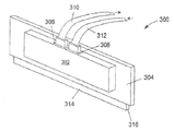
특정 구현예에서, 제1 및 제2 광학/전자 인터페이스(202 및 208)는 확장 DIMM 상에 구현될 수 있다. 도 3a는 본 발명의 구현예에 따라 구성된 확장 DIMM(300)의 사시도이다. 확장 DIMM(300)은 기판(304)상에 배치된 확장 요소(302)를 포함한다. 확장 요소(302)는 두 개의 광학 포트(306 및 308)를 포함하는 광학 인터페이스(도시되지 않음) 및 전자 인터페이스(도시되지 않음)를 포함한다. 전자 인터페이스(도시되지 않음)는, 아래에 설명된 바와 같이, DDRx 인터페이스를 통하여 확장 DIMM으로 전송되고 확장 DIMM으로부터 전송되는 데이터를 인코딩하는 전자 신호의 병렬-직렬(parallel-to-serial) 및 직렬-병렬(serial-to-parallel) 흐름 제어를 수행한다. 도 3a는 광학 포트(306 및 308) 각각에 삽입된 도파로(waveguide)(310 및 312)를 도시한다. "도파로"라는 용어는 광학 신호를 송신하기 위한 광 섬유, 광 리본, 또는 임의의 기타 적절한 매체를 말한다. 기판(304)은, 기판(304)의 커넥터(connector)부(316)를 따라 위치한 핀(314)에 연결된 신호 선(signal line)을 포함한다. 커넥터부(316) 상에 인쇄된 핀(314)의 개수는 주 보드에 탑재된 DIMM 슬롯의 유형에 따라 다양할 수 있다. 예를 들면, 핀(314)의 개수는 64, 72, 100, 144, 168, 및 184 또는 그 이상이 될 수 있다. 일반적으로, DDRJC 인터페이스를 통하여 확장 DIMM(300)에 전송되는 전자 신호는 전자 인터페이스(도시되지 않음)에 의하여 처리되고, 전자 신호를 도파로(310)을 통하여 출력되는 광학 신호로 변환하는 광학 인터페이스(도시되지 않음)에 전송된다. 광학 인터페이스(도시되지 않음)는 도파로(312)에 수신된 광학 신호를, 전자 인터페이스(도시되지 않음)에 의하여 처리되고 DDRx 인터페이스를 통하여 마더보드 상에 위치한 프로세서 또는 메모리로 전송되는 전자 신호로 변환한다.In certain implementations, the first and second optical /
도 3b는 본 발명의 구현예에 따라 DIMM 슬롯(318)에 장착된 확장 DIMM(300)의 사시도이다. 마더보드(320)는 메모리 확장 보드, 워크스테이션, 하이엔드(high-end) 데스크톱 컴퓨터, 서버 블레이드, 또는 네트워크 인터페이스의 마더보드일 수 있다. 마더보드(320)상에 배치된 메모리(322)는 DIMM 슬롯(328 내지 330)에 각각 장착된 세 개의 DIMM(324 내지 326)을 포함한다. DIMM 슬롯(318)은 DIMM 슬롯(328 내지 330)과 동일하다. 따라서, 어댑터(adaptor) DIMM(300)은 DIMM(324 내지 326)의 어느 하나를 교체하면서 다른 DIMM 슬롯(328 내지 330)의 어디에나 장착될 수 있다. 확장 DIMM(300)은 마더보드(320)의 성능에 영향을 주지 않으며, 마더보드(320)가 구성되는 때에, 또는 향후 기존의 메모리 용량이 불충분하게 되는 때에, DIMM 슬롯에 장착될 수 있다. 도 3b에 도시된 바와 같이, 확장 DIMM(300)이 다른 DIMM(324 내지 326) 옆에 장착될 수 있음에도 불구하고, 확장 DIMM(300)은 다른 DIMM(324 내지 326)과 비교하여 전기적 로딩의 함수로서 상대적으로 감소된 최대 데이터 레이트(data rate)를 가질 수 있다.3B is a perspective view of an expanded
다른 구현예에서, 제1 및 제2 광학/전자 인터페이스(202 및 208)는 마더보드의 소켓에 삽입된 칩에 구현될 수 있다. 도 4는 본 발명의 구현예에 따라 마더보드(406)의 소켓(404)에 삽입된 광학/전자 인터페이스 칩(402)의 사시도이다. 칩(402)은, 아래에 설명한 바와 같이, 광학 입력 포트(408) 및 광학 출력 포트(410)을 가지는 광학 인터페이스(도시되지 않음), 및 하나 이상의 DDRx 인터페이스를 통하여 칩(402)에 전송되고 칩(402)으로부터 전송되는 데이터를 인코딩하는 전자 신호의 병렬-직렬 및 직렬-병렬 흐름 제어를 수행하는 전자 인터페이스(도시되지 않음)로 구성되어 있다. 광학 인터페이스는 칩(402)에 의하여 처리되는 전자 신호를 도파로(410)에 출력되는 광학 신호로 변환하고, 또한 도파로(408)에서 칩(402)로 전송되는 광학 신호를 전자 인터페이스에 의하여 처리될 수 있고 마더보드(406) 상에 위치한 프로세서 또는 기타 메모리에 전송될 수 있는 전자 신호로 변환한다.In other implementations, the first and second optical /
도 5 내지 도 9는 제1 및 제2 광학/전자 인터페이스(202 및 208)가 본 발명의 확장 메모리 시스템 구현예에 구현될 수 있는 다양한 방법의 개략도이다.5-9 are schematic diagrams of various methods in which the first and second optical /
도 5는 본 발명의 구현예에 따라 구성된 제1 확장 메모리 시스템(500)의 개략도이다. 시스템(500)은 주 보드(504)의 DIMM 슬롯에 장착된 제1 확장 DIMM(502)을 포함한다. 제1 확장 DIMM(502)은 전자 인터페이스(506) 및 광학 인터페이스(508)을 포함한다. 전자 인터페이스(506)는 제1 DDRx 인터페이스(512)를 통하여 프로세서(510)와 전자 통신을 하고, 광학 인터페이스(508)와 전자 통신을 한다. 도 5에 도시된 바와 같이, 시스템(500)은 제2 확장 DIMM(514) 및 메모리 확장 보드(516)를 포함한다. 제2 확장 DIMM(514)은 메모리 확장 보드(516)의 DIMM 슬롯에 장착되고, 제2 DDRx 인터페이스(526)을 통하여 두 개의 DIMM(522 및 524)와 전자 통신을 하고 광학 인터페이스(518)와 전자 통신을 하는, 전자 인터페이스(520) 및 광학 인터페이스(518)를 포함한다. 도 5는 또한 제1 및 제2 확장 DIMM(502 및 514)이 광학적으로 인터페이스(508 및 518)를 연결하는 도파로(528 및 530)를 통하여 광학 통신을 함을 나타낸다. 시스템(500)은 메모리 확장 보드(516)의 DIMM 슬롯에 장착될 수 있는 가장 큰 메모리에 대한 2:1 확장을 제공한다.5 is a schematic diagram of a first
프로세서(510)가 데이터를 DIMM(522 및 524)에 저장할 때, 프로세서(510)는 데이터, 주소, 및 제어 정보를 포함하는 병렬 전자 신호를 DDRx 인터페이스(512)를 통하여 제1 확장 DIMM(502)으로 전송한다. 전자 인터페이스(506)는 병렬 전자 신호를 직렬 전자 신호로 변환함으로써 병렬-직렬 흐름 제어를 수행하고, 데이터가 프로세서(510)로부터 출력되는 속도의 변화를 보상(compensate)하기 위하여, 전자 신호에 인코딩된 정보를 저장하는 메모리 버퍼를 포함한다. 직렬 전자 신호는 광학 인터페이스(508)에 전송되고, 동일한 정보를 인코딩하는 광학 신호로 변환되며, 광학 신호는 도파로(530)를 통하여, 광학 신호를 제2 전자 인터페이스(520)에 전송되는 직렬 전자 신호로 다시 변환시키는 광학 인터페이스(518)에 전송된다. 전자 인터페이스(520)는 직렬 전자 신호를 병렬 전자 신호로 변환함으로써 직렬-병렬 흐름 제어를 수행하고, 데이터가 제1 확장 DIMM(502)으로부터 전송되는 속도의 변화를 보상하기 위하여, 전자 신호에 인코딩된 정보를 저장하는 메모리 버퍼를 포함한다. 병렬 전자 신호는 DIMM(522 및 524)에 저장되기 위해 DDRx 인터페이스(526)를 통하여 전송된다.When
DDRx 인터페이스(526)를 통하여 병렬 전자 신호를 확장 DIMM(514)에 전송함으로써, DIMM(522 및 524)에 저장된 데이터는 프로세서(510)로 전송된다. 이러한 경우에, 전자 인터페이스(520)는 병렬 전자 신호를 직렬 전자 신호로 변환함으로써 병렬-직렬 흐름 제어를 수행하고, 데이터가 DIMM(522 및 524)으로부터 전송되는 속도의 변화를 보상하기 위하여, 메모리 버퍼에 정보를 저장할 수 있다. 상기 정보는 직렬 전자 신호로 인코딩되어 전자 인터페이스(520)로부터 광학 인터페이스(518)로 전송되고, 도파로(528)을 통하여 광학 인터페이스(508)에 전송되는 광학 신호로 변환된다. 광학 인터페이스(508)는 광학 신호를, 제1 전자 인터페이스(506)로 전송되는 직렬 전자 신호로 다시 변환한다. 전자 인터페이스(506)는 직렬 전자 신호에 인코딩된 정보를, 데이터가 제2 확장 DIMM(514)으로부터 전송되는 속도의 변화를 보상하기 위하여, 메모리 버퍼에 저장함으로써 직렬-병렬 흐름 제어를 수행한다. 전자 인터페이스(506)는 상기 정보를, 처리를 위해 제1 DDRx 인터페이스(512)를 통하여 프로세서(510)로 전송되는 병렬 전자 신호로 변환한다.The data stored in
도 6은 본 발명의 구현예에 따라 구성된 제2 확장 메모리 시스템(600)의 개략도이다. 상기 시스템(600)은 제2 확장 DIMM(514)이 주문형 반도체(application specific integrated circuit, ASIC)(602)로 교체가 된 점 및 메모리 확장 보드(516)가 메모리 확장 보드(604)와 상이하게 구성되어 있는 점을 제외하고는 시스템(500)과 거의 동일하다. 도 4를 참조하여 위에서 설명한 바와 같이, ASIC(602)은 보드에 탑재된 칩으로서 구현되고, 하나 이상의 DIMM 세트와 전자 통신을 하는 팬-아웃(fan-out)을 가지도록 구성될 수 있다. 예를 들면, 도 6에 도시된 바와 같이, ASIC(602)은 두 개의 세트의 DIMM과 전자 통신을 하는 팬-아웃과 팬-인(fan-in)을 가지도록 구성된다. 구체적으로, ASIC(602)은 DDRx 인터페이스(608)를 통하여 DIMM(604 및 606)과 전자 통신을 하고, 다른 DDRx 인터페이스(614)를 통하여 DIMM(610 및 612)과 전자 통신을 한다. ASIC(602)은 광학 인터페이스(616) 및 전자 인터페이스(618)로 구성된다. 도 5를 참조하여 위에 설명한 바와 같이, 광학 인터페이스(508 및 616)는 도파로(528 및 530)을 통하여, 제2 확장 DIMM(514)의 광학 인터페이스(518)와 동일한 기능을 수행하는 광학 인터페이스(616)와 광학 통신을 한다. 전자 인터페이스(618)는 또한 확장 DIMM(514)의 전자 인터페이스(520)와 동일한 기능을 수행한다.6 is a schematic diagram of a second
데이터는, 도 5를 참조하여 위에서 설명한 동일한 병렬-직렬 흐름 제어 방법으로, 주 보드(504)의 프로세서(510)로부터 도파로(530)을 통하여 메모리 확장 보드(604)의 메모리로 전송된다. 광학 인터페이스(616)는 광학 인터페이스(508)로부터 수신한 광학 신호를 직렬 전자 신호로 다시 변환하고, 도 5를 참조하여 위에서 설명한 확장 DIMM(514)의 전자 인터페이스(520)에 의하여 수행되는 것과 대체로 동일한 직렬-병렬 흐름 제어를 수행한다. 그러나, 제2 확장 DIMM(514)과 다르게, 전자 인터페이스(602)는 정보를 DIMM(604, 606, 610, 또는 612)에 저장하기 위해 DDRx 인터페이스(608 및 614)를 통하여 전송될 수 있는 병렬 전자 신호로 변환한다.The data is transferred from the
DIMM(604, 606, 610, 또는 612)에 저장된 데이터는 연관된 DDRx 인터페이스(608 및 614)를 통하여 병렬 전자 신호를 ASIC(602)에 전송함으로써 프로세서(510)로 전송된다. 전자 인터페이스(618)는, 도 5를 참조하여 위에서 설명한 바와 같이, 제2 확장 DIMM(514)이 수행하는 것과 대체로 동일한 병렬-직렬 흐름 제어를 수행한다. 상기 정보는 직렬 전자 신호에 인코딩되고, 전자 인터페이스(618)로부터 광학 인터페이스(616)로 전송되며, 도파로(528)를 통하여 광학 인터페이스(508)로 전송되는 광학 신호로 변환된다. 광학 신호는 도 5를 참조하여 위에서 설명한 바와 같이 처리된다.Data stored in the
도 7은 본 발명의 구현예에 따라 구성된 제3 확장 메모리 시스템(700)의 개략도이다. 상기 시스템(700)은 주 보드(704) 상에 탑재된 제1 ASIC(702)을 포함한다. 제1 ASIC(702)은 전자 인터페이스(706) 및 광학 인터페이스(708)를 포함한다. 전자 인터페이스(706)는 DDRx 인터페이스(712)를 통하여 프로세서(710)와 전자 통신을 하고, 광학 인터페이스(708)와 전자 통신을 한다. 도 7에 도시된 바와 같이, 시스템(700)은, 도 6을 참조하여 위에서 설명한, 제2 ASIC(602) 및 메모리 확장 보드(604)를 포함한다.7 is a schematic diagram of a third
데이터는, 도 5 및 도 6을 참조하여 위에서 설명한 것과 동일한 병렬-직렬 및 직렬-병렬 흐름 제어 방법으로 도파로(528 및 530)를 통하여 프로세서(710) 및 메모리 확장 보드(604)의 메모리 사이에서 전송된다.The data is transferred between the memory of the
도 8은 본 발명의 구현예에 따라 구성된 제4 확장 메모리 시스템(800)의 개략도이다. 상기 시스템(800)은 도 5를 참조하여 위에서 설명한 주 보드(504)의 DIMM 슬롯에 장착된 동일한 제1 확장 DIMM(502)을 포함한다. 상기 시스템(800)은 또한 네 개의 광학-DDR ASIC(optical-to-DDR ASIC)(806 내지 809)과 광학 통신을 하는 광학 버스(804)를 포함하는 메모리 확장 보드(802)를 포함한다. 광학 버스(804)는 팬-인 버스(810) 및 팬-아웃 버스(812)를 포함하고, 이들 모두는, 광학 탭(optical tap)(823)과 같은, (도 8에서 OT로 식별되는) 광학 탭을 통하여 ASIC(806 내지 809)와 광학 통신을 한다. 팬-인 버스(810) 및 팬-아웃 버스(812)는 광학 신호를 송신하기 위한 다중모드(multi-mode) 광 섬유, 리지 도파로(ridge waveguide), 광 결정 도파로(photonic crystal waveguide), 공동 도파로(hollow waveguide) 또는 임의의 기타 적합한 다중모드 매체가 될 수 있다. 공동 도파로는 공심(air core)이 있는 관(tube)으로 구성될 수 있다. 공동 도파로를 형성하는 구조 관(structural tube)은 굴절률이 1보다 크거나 작은 내부 중심(core) 물질을 가질 수 있다. 관은, 높은 반사율을 제공하는 관의 내부 표면 상에 침전될 수 있는 적절한 금속, 유리, 또는 플라스틱 및 금속 및 유전체 필름으로 구성될 수 있다. 공동 도파로는 중심의 내부 표면을 그리는(lining) 높은 반사율을 가지는 금속 코팅이 된 공동 금속 도파로일 수 있다. 공심은 빛을 유도(guide)하기에 적합한 원형, 타원형, 정사각형, 직사각형, 또는 임의의 다른 모양의 단면 모양을 가질 수 있다. 도파로는 속이 비어있기(hollow) 때문에, 광학 신호는 유효 인덱스(effective index)가 약 1인 공동 도파로의 중심을 따라 진행할 수 있다. 다시 말해서, 빛은 공기가 있는 경우 또는 진공에서의 빛의 속도로 공동 도파로의 중심을 따라 전파된다. 광학 탭은 버스(810 및 812)를 따라 송신되는 광학 신호의 특정 부분을 반사하고 송신하도록 구성될 수 있는 빔 분리기(beam splitter), 부분적으로 반사 거울, 또는 임의의 기타 매체일 수 있다. 각각의 광학-DDR ASIC은 DDRx 인터페이스를 통하여 네 개의 연관된 DIMM과 전자 통신을 한다. 예를 들면, ASIC(806)은 DDRx 인터페이스(816 및 818)를 통하여 DIMM(814)과 전자 통신을 한다.FIG. 8 is a schematic diagram of a fourth
팬-아웃 버스(812)의 광학 탭(820 내지 823)은 ASIC(806 내지 809) 사이에 거의 동일하게 광전력을 분배하도록 구성되어 있다. 일반적으로, 광학 탭은 광학 인터페이스(508)로부터의 광학 신호 출력의 총 광전력의 약 1/n(여기서, n은 광학-DDR ASIC의 개수)을 각각의 광학-DDR ASIC으로 나누어주도록(divert) 구성되어 있다. 예를 들면, 광학 탭(823)은 광학 버스(812)에 의하여 수송되는 광전력의 약 1/4을 ASIC(809)으로 보내고, 광학 탭(822)은 광학 버스(812)에 의하여 수송되는 광전력의 약 1/3을 ASIC(808)으로 보내고, 광학 탭(821)은 광학 버스(812)에 의하여 수송되는 나머지 광전력의 약 1/2을 ASIC(807)으로 보내며, 광학 탭(820)은 전반사 거울이다. 한편, 팬-인 버스(810)의 광학 탭(824 내지 827)은 광학 인터페이스(508)에 의하여 각각의 ASIC(806 내지 809)로부터 동일한 양의 광전력이 수신되도록 구성되어 있다. 일반적으로, 팬-인 버스의 n개의 광학 탭은 광학 인터페이스가 n 개의 광학-DDR ASIC 각각으로부터 총 광전력 출력의 약 1/n을 수신하도록 구성되어 있다. 예를 들면, 광학 탭(824 내지 827)은 모두 광학 인터페이스(508)에 의하여 수신된 광학 신호의 광전력이 대략 각각의 ASIC(806 내지 809)으로부터의 광학 신호 출력의 전력의 1/4이 되도록 구성되어 있다.The optical taps 820-823 of the fan-out
메모리 확장 보드(802)는 팬-인 및 팬-아웃 도파로(810 및 812)와 광학 통신을 하는 중계기(repeater)(도시되지 않음)를 포함할 수 있다. 중계기는 광학 신호를 수신하고, 광학 신호를 다시 발생시키고, 그 후 다시 발생된 광학 신호를 재송신하는, 광학-전자-광학 변환기(optical-to-electrical-to-optical converter)이다. 중계기는 자유 공간(free-space) 또는 광학 상호연결 손실(optical interconnect loss)로 인한 감쇠(attenuation)를 극복하기 위하여 사용될 수 있다. 광학 신호를 강화시킬 뿐 아니라, 중계기는 광학 신호의 잡음 또는 기타 원치 않는 양상을 제거하기 위하여 또한 사용될 수 있다. 중계기에 의하여 생성된 광전력의 양은 팬-아웃 버스에 부착된 ASIC의 개수, 시스템 손실(system loss), 및 ASIC에서의 광학 수신기 감도에 의하여 결정된다. 다시 말해서, 중계기는 모든 ASIC에 도달할 정도의 충분한 광전력을 가지는 광학 신호를 발생시키기 위하여 사용될 수 있다.The
프로세서(510)로부터 전송된 데이터는 데이터의 저장을 처리할 광학-DDR ASIC의 추가적인 주소를 포함한다. 데이터는 생성되고 도 5를 참조하여 위에서 설명한 병렬-직렬 흐름 제어 방법과 동일한 방법으로 프로세서로부터 팬-아웃 버스(812)로 전송된다. 광학 신호는 팬-아웃 버스(812)에 직접 주입(inject)되고, 광학 탭(820 내지 823)은 광학 신호의 일부를 연관된 ASIC(806 내지 809)로 보내며, ASIC(806 내지 809)이 데이터를 수신하게 될 ASIC을 식별하는 전자 신호의 주소 부분을 분석하는 추가적인 단계를 수행한다는 점을 제외하고는, 상기 ASIC은 도 6의 ASIC(602)를 참조하여 위에서 설명한 직렬-병렬 흐름 제어와 동일한 방법으로 수행하도록 구성되고 동작한다. 상기 주소가 수신하는 ASIC의 주소와 상응하지 않는 경우에, 데이터는 폐기될 수 있다. 그러나, 상기 주소가 수신하는 ASIC의 주소와 합치(match)하는 경우에는, ASIC은 연관된 DIMM에 데이터를 저장함으로써 데이터를 처리한다.The data transmitted from the
메모리 확장 보드(802)의 DIMM에 저장된 데이터를 전송하기 위하여, 중재기(arbiter)가 사용되어 두 개 이상의 ASIC이 동시에 팬-인 버스(810)를 사용하는 것을 방지할 수 있다. 중재(arbitration)가 없이는, 광학 인터페이스(508)는 도파로(528) 상으로 두 개 이상의 ASIC으로부터 광학 신호를 수신할 수 있고, 광학 신호는 광학 인터페이스(508)에서 해독할 수 없도록 결합되어 도착한다. 중재기는, 팬-인 버스(810)가 사용될 수 있기 이전에, ASIC이 팬-인 버스(810)를 사용할 권한을 획득하였음을 보장하여, 동시에 광학 신호를 송신하는 것을 방지한다. 중재는 팬-인 버스에 다수의 ASIC이 추가됨에 따라 상대적으로 빨라지고 조정된다. 중재는 잘 알려진 광학 또는 전자, 토큰 기반(token-based)의 중재 방법을 사용하는 중재기에 의하여 수행될 수 있다. 일단 ASIC들(806 내지 809) 중 하나가 팬-인 버스(810)를 사용할 권한을 획득하면, 도 6을 참조하여 위에서 설명한 바와 같이, 연관된 DIMM에 저장된 데이터를 생성하는 광학 신호가 발생되고, 팬-인 버스(810) 및 도파로(528)를 통하여 광학 인터페이스(508)로 전송된다. 상기 데이터는 도 5를 참조하여 위에서 설명한 바와 같이 프로세서(510)에 의하여 수신된다.In order to transfer data stored in the DIMMs of the
도 9는 본 발명의 구현예에 따라 구성된 제5 확장 메모리 시스템(900)의 개략도이다. 상기 시스템(900)은 도 7을 참조하여 위에서 설명한 주 보드(704)의 ASIC(702)과 동일한 것을 포함하고, 상기 시스템(900)은 도 8을 참조하여 위에서 설명한 바와 같이 구성된 메모리 확장 보드(802)와 동일한 것을 포함한다. ASIC(702) 및 주 보드(704)는 도 7을 참조하여 위에서 설명한 바와 같이 동작하고, 메모리 확장 보드(802)의 구성요소는 도 8을 참조하여 위에서 설명한 바와 같이 구성되고 동작한다.9 is a schematic diagram of a fifth extended memory system 900 constructed in accordance with an embodiment of the present invention. The system 900 includes the same as the
도 10은 본 발명의 구현예에 따라 구성된 광학/전자 인터페이스(1000)의 블록도이다. 인터페이스(1000)는 광학 인터페이스(1002), 전자 인터페이스(1004), 및 핀(1006)을 포함한다. 핀(1006)은, 도 3 및 도 4를 참조하여 위에서 설명한 바와 같이, DIMM 슬롯 또는 소켓을 통하여 마더보드의 하나 이상의 DDRx 인터페이스와 전자적으로 연결되어 있다. 핀(1006)은 하나 이상의 DDRx 인터페이스의 병렬 신호 선으로부터 데이터, 주소, 및 제어 정보를 인코딩하는 병렬 전자 신호(1008)를 수신하고, 병렬 전자 신호(1008)를 전자 인터페이스(1004)의 직렬화 블록(1010)에 전송한다. 직렬화 블록(1010)은 병렬 전자 신호(1008)를 수신하고 동일한 정보를 인코딩하는 직렬 전자 신호(1012)로 변환하는 전자 구성요소를 포함한다. 직렬화 블록(1010)은 선택적으로 직렬 전자 신호(1012)에 DC 균형(DC balanced) 코딩을 사용할 수 있다. DC 균형 코딩은 같은 수의 논리 "1" 및 논리 "0"을 가진 코드 워드(cord word)를 생성하기 위하여 사용될 수 있다. DC 균형 코딩은 맨체스터 코딩(Manchester coding) 및 그 변형을 포함한다. 맨체스터 코딩에서, 논리 "0"은 비트 중앙에서의 "0"에서 "1"로의 전이(transition)로 식별되고, 논리 "1"은 비트 중앙에서의 "1"에서 "0"으로의 전이로서 표시된다. 4B/6B DC 균형 코딩에서, 코드 워드는 DC 균형을 제공하기 위하여 세 개의 논리 "1" 및 세 개의 논리 "0"을 포함한다. 4B/8B DC 균형 코딩에서, 8 비트의 코드 워드는 세 개 이상의 연속된 논리 "1" 및 논리 "0"이 없도록 하면서 네 개의 논리 "1" 및 네 개의 논리 "0"을 가진다. 8B/10B DC 균형 코딩에서는, 8 비트의 데이터가 심볼 또는 캐릭터라고 명명되는 10 비트의 개체(entity)로서 전송된다. 데이터의 하위 5 비트는 6 비트 그룹(5B/6B 부분)으로 인코딩되고, 상위 3 비트는 4 비트 그룹(3B/4B 부분)으로 인코딩된다. 이러한 코드 그룹은 함께 이어져서 10 비트 심볼을 형성한다. 두 개의 추가적인 비트는 시간이 지남에 따라 데이터 스트림에서 전송되는 "0" 및 "1"의 개수가 균형이 맞추어지도록 한다. 직렬 전자 신호(1012)를 광학 인터페이스(1002)의 광학 송신기(1014)로 전송하기 이전에, 정보는 데이터가 수신되는 속도 및 데이터가 전송되는 속도의 변화를 보상하기 위하여 메모리 버퍼(1016)에 임시로 저장될 수 있다. 광학 송신기(1014)는 직렬 전자 신호(1012)를 동일한 정보를 인코딩하는 광학 신호(1016)로 변환하고, 광학 신호는, 위에서 설명한 도파로(310 및 410)와 같은, 도파로를 통하여 송신된다. 광학 송신기(1014)는 수직 공진형 표면 발광 레이저(vertical cavity surface emitting laser, VCSEL), 이중 헤테로구조 레이저(double heterostructure laser), 양자 우물 레이저(quantum well laser), 양자 계단 레이저(quantum cascade laser), 분포 귀환 레이저(distributed feedback laser), 또는 임의의 기타 반도체 기반 레이저일 수 있다.10 is a block diagram of an optical /
도 10에 도시된 바와 같이, 광학 인터페이스(1002)는 정보를 인코딩하는 광학 신호(1020)를 수신하는 광학 수신기(1018)를 또한 포함한다. 광학 수신기(1018)는 광학 신호(1020)를 동일한 정보를 인코딩하는 직렬 전자 신호(1022)로 변환하는 pn 또는 p-i-n 접합 광다이오드일 수 있다. 예를 들면, 광학 수신기(1018)는 칩 상에 집적된 비소화 갈륨(GaAs), 비소화 인듐 갈륨(InGaAs), 실리콘(Si), 게르마늄(Ge), 또는 실리콘 게르마늄(SiGe) 기반의 광다이오드가 될 수 있다. 전자 인터페이스(1004)는 직렬 전자 신호(1022)를 수신하고, 직렬 전자 신호(1022)의 DC 균형 코딩을 디코딩하고, 직렬 전자 신호(1022)를 DDRx 인터페이스를 통한 송신을 위한 핀(1006)으로 송신되는 병렬 전자 신호(1026)로 변환하는 전자 구성요소를 포함하는 병렬화 블록(deserialization block)(1024)을 포함한다. 상기 정보는 또한, 병렬 전자 신호(1026)를 발생시키기 전에, 메모리 버퍼(1016)에 임시로 저장될 수 있다.10, the
도파로(528 및 530)는 메모리 확장 보드가 광학적으로 주 보드에 연결될 수 있는 수많은 방법 중 대표적인 하나일 뿐이다. 예를 들면, 메모리 확장 보드 및 주 보드는, 동일한 캐비닛에 탑재된 다른 보드 사이에 전자 및 광학 연결을 제공하기 위하여 또한 사용되는 캐비닛 백플레인(backplane)을 통하여 광학적으로 상호연결될 수 있다. 도 11은 캐비닛 백플레인(1102)를 통하여 광학 통신을 하는 주 보드(204) 및 메모리 확장 보드(212)의 사시도 및 개략도이다. 명확하게 나타내기 위하여 다른 보드 및 캐비닛의 일부는 도시되지 않았다. 백플레인(1102)은 섬유 리본 커넥터(1104 내지 1107)를 포함할 수 있다. 도 11에 도시된 바와 같이, 광학/전자 인터페이스(208)는 섬유 리본(1108 및 1109)를 통하여 커넥터(1104 및 1105)에 광학적으로 연결되어 있고, 광학/전자 인터페이스(202)는 섬유 리본(1110 및 1111)을 통하여 커넥터(1106 및 1107)에 광학적으로 연결되어 있다. 백플레인(1102)은, 위에서 설명한 바와 같이, 광학 신호(214 및 216)를 교환하기 위한 광학/전자 인터페이스(202 및 208)를 가능하게 하는, 광학적으로 커넥터(1104 및 1106)를 연결하고, 광학적으로 커넥터(1105 및 1107)을 연결하는 광학 섬유로 구성되어 있다.
전자 신호를 송신, 직렬화, 및 병렬화하기 위하여 사용되는 DDRx 및 전자 인터페이스는 광학 인터페이스 사이에 송신되는 광학 신호에서의 속도보다 상대적으로 낮은 데이터 송신 속도로 수행됨에 유의할 것이다. 예를 들면, 도파로(528 및 530) 또는 백플레인(1102)를 통하여 송신되는 광학 신호는 클록 레이트의 대략 4배 내지 6배로 송신될 수 있다. 다시 말해서, 고속 데이터 송신은 광학 인터페이스 사이에서 달성되고, 상대적으로 낮은 속도의 송신은 DDRx 및 전자 인터페이스와 같은 전자 구성요소에 의하여 수행된다.It will be noted that the DDRx and the electronic interface used to transmit, serialize, and parallelize the electronic signal are performed at a data transmission rate that is relatively lower than the speed in the optical signal transmitted between the optical interfaces. For example, optical signals transmitted through the
도 12는 본 발명의 구현예에 따른 확장 메모리 시스템에서 데이터를 전송하기 위한 방법의 제어 흐름도이다. 단계 1201에서, 도 5 내지 도 10을 참조하여 위에서 설명한 바와 같이, 병렬 전자 신호는 DDRx 인터페이스로부터 수신된다. 병렬 전자 신호는 프로세서 또는 로컬 메모리에 의하여 발생될 수 있다. 단계 1202에서, 병렬 전자 신호는, 도 10의 직렬화 블록(1010)을 참조하고 도 5 내지 도 9를 참조하여 위에서 설명한 바와 같이, 병렬 전자 신호를 동일한 정보를 인코딩하는 직렬 전자 신호로 변환함으로써 직렬화된다. 선택적인 단계 1203에서, 직렬 전자 신호는, 도 10의 직렬화 블록(1010)을 참조하여 위에서 설명한 바와 같이, DC 균형을 포함하도록 인코딩될 수 있다. 선택적인 단계 1204에서, 도 10의 단계 1014를 참조하여 위에서 설명한 바와 같이, 데이터가 수신 및/또는 전송되는 속도의 변화를 보상하기 위하여, 전자 신호에 인코딩된 정보는 메모리 버퍼에 저장될 수 있다. 단계 1205에서, 도 10을 참조하여 위에서 설명한 바와 같이, 데이터를 인코딩하는 직렬 전자 신호는 광학 송신기로 전송된다. 단계 1206에서, 광학 송신기는 직렬 전자 신호를 도파로를 통하여 주 보드 또는 확장 메모리 시스템의 광학/전자 인터페이스로 전송되는 광학 신호로 변환한다.12 is a control flow diagram of a method for transferring data in an extended memory system according to an embodiment of the present invention. At
도 13은 본 발명의 구현예에 따른 확장 메모리 시스템에서 데이터를 수신하기 위한 방법의 제어 흐름도이다. 단계 1301에서, 도 10의 광학 신호(1024)를 참조하여 위에서 설명한 바와 같이, 주 보드 또는 메모리 확장 보드로부터 전송된 광학 신호는 수신되고 직렬 전자 신호로 변환된다. 단계 1302에서, 도 10의 병렬화 블록(1028)을 참조하여 위에서 설명한 바와 같이, 직렬 전자 신호는 병렬화 블록을 사용하여 병렬 전자 신호로 변환된다. 선택적인 단계 1303에서, 도 10을 참조하여 위에서 설명한 바와 같이, 광학 신호가 DC 균형 코딩을 사용하여 전송되는 경우에, DC 균형 코딩은 병렬 전자 신호로부터 제거된다. 선택적인 단계 1304에서, 데이터가 수신되는 속도 및 데이터가 전송될 수 있는 속도의 변화를 보상하기 위하여 병렬 전자 신호는 메모리 버퍼에 저장될 수 있다. 단계 1305에서, 데이터를 인코딩하는 병렬 전자 신호는 DDRx 인터페이스를 통하여 주 보드의 프로세서 또는 메모리 확장 보드의 메모리로 송신될 수 있다.13 is a control flow diagram of a method for receiving data in an extended memory system in accordance with an embodiment of the present invention. In
설명의 목적을 가진 상기 상세한 설명에서는 본 발명에 대한 깊은 이해를 제공하기 위해 특정한 명명법을 사용하였다. 그럼에도, 해당 기술 분야의 당업자에게 본 발명을 실시하기 위해서 구체적인 세부내용들이 요구되지는 않는다는 것이 명백할 것이다. 상기 본 발명의 특정한 구현예에 대한 상세한 설명들은 이해 및 설명의 목적으로 제시된다. 이들은 본 발명의 완성된 형태이거나 개시된 특정 형태로 본 발명을 제한하는 것을 의도하지 않는다. 명백히, 많은 변형 및 변경이 상기 교시로부터 가능하다. 구현예들은 본 발명의 원칙 및 이의 실제 적용분야를 최적으로 설명하기 위해 나타내지고 설명되었으며, 따라서 해당 기술 분야의 당업자로 하여금 고려되는 특정 용도에 적합하게 본 발명 및 각종 변형된 각종 구현예들을 최적으로 이용할 수 있게 한다. 본 발명의 범위는 첨부된 청구항 및 그들의 동등물에 의해 규정되는 것이 의도된다.In the foregoing detailed description, for purposes of explanation, specific nomenclature is used to provide a deeper understanding of the present invention. Nevertheless, it will be apparent to those skilled in the art that specific details are not required to practice the invention. The foregoing detailed description of certain embodiments of the invention has been presented for purposes of understanding and illustration. They are neither a complete description of the invention nor are intended to limit the invention to the particular form disclosed. Obviously, many modifications and variations are possible from the above teachings. The embodiments have been shown and described in order to best explain the principles of the invention and its practical application and, accordingly, it is to be understood that those skilled in the art will be able to select the most suitable embodiments of the invention and various modified embodiments . It is intended that the scope of the invention be defined by the appended claims and their equivalents.
102: 메모리 104: 프로세서
106: 마더보드 108, 109, 110, 111: DIMM
112, 113, 114, 115: DIMM 슬롯 118: DDR 인터페이스
200: 확장 메모리 시스템 202: 제1 광학/전자 인터페이스
204: 주 보드 206: 프로세서
208: 제2 광학/전자 인터페이스 210: 메모리
212: 메모리 확장 보드 214, 216: 광학 신호
300: 확장 DIMM 302: 확장 요소
304: 기판 306, 308: 광학 포트
310, 312: 도파로 314: 핀
316: 커넥터부 318: DIMM 슬롯
320: 마더보드 322: 메모리
324, 325, 326: DIMM 328, 329, 330: DIMM 슬롯
402: 광학/전자 인터페이스 칩 404: 소켓
406: 마더보드 408: 도파로, 광학 입력 포트
410: 도파로, 광학 출력 포트
500: 제1 확장 메모리 시스템 502: 제1 확장 DIMM
504: 주 보드 506, 520: 전자 인터페이스
508, 518: 광학 인터페이스 510: 프로세서
512: 제1 DDRx 인터페이스 514: 제2 확장 DIMM
516: 메모리 확장 보드 522, 524: DIMM
526: 제2 DDRx 인터페이스 528, 530: 도파로
600: 제2 확장 메모리 시스템 602: ASIC
604: 메모리 확장 보드 606, 610, 612: DIMM
608, 614: DDRx 인터페이스 616: 광학 인터페이스
618: 전자 인터페이스
700: 제3 확장 메모리 시스템 702: ASIC
704: 주 보드 706: 전자 인터페이스
708: 광학 인터페이스 710: 프로세서
712: DDRx 인터페이스
800: 제4 확장 메모리 시스템 802: 메모리 확장 보드
804: 광학 버스 806, 807, 808, 809: 광학-DDR ASIC
810: 팬-인 버스 812: 팬-아웃 버스
814: DIMM 816, 818: DDRx 인터페이스
820, 821, 822, 823, 824, 825, 826, 827: 광학 탭
900: 제5 확장 메모리 시스템
1000: 광학/전자 인터페이스 1002: 광학 인터페이스
1004: 전자 인터페이스 1006: 핀
1008: 병렬 전자 신호 1010: 직렬화 블록
1012: 직렬 전자 신호 1014: 광학 송신기
1016: 광학 신호 1016: 메모리 버퍼
1018: 광학 수신기 1020: 광학 신호
1022: 직렬 전자 신호 1024: 병렬화 블록
1026: 병렬 전자 신호 1102: 백플레인
1104, 1105, 1106, 1107: 섬유 리본 커넥터
1108, 1109, 1110, 1111: 섬유 리본102: memory 104: processor
106:
112, 113, 114, 115: DIMM slot 118: DDR interface
200: Extended memory system 202: First optical / electronic interface
204: main board 206: processor
208: second optical / electronic interface 210: memory
212:
300: Expansion DIMM 302: Expansion element
304:
310, 312: waveguide 314: pin
316: connector portion 318: DIMM slot
320: Motherboard 322: Memory
324, 325, 326:
402: Optical / electronic interface chip 404: Socket
406: motherboard 408: waveguide, optical input port
410: waveguide, optical output port
500: first extended memory system 502: first extended DIMM
504:
508, 518: Optical interface 510: Processor
512: first DDRx interface 514: second extended DIMM
516:
526:
600: second extended memory system 602: ASIC
604:
608, 614: DDRx interface 616: Optical interface
618: Electronic interface
700: third extended memory system 702: ASIC
704: Main board 706: Electronic interface
708: Optical interface 710: Processor
712: DDRx interface
800: fourth expansion memory system 802: memory expansion board
804:
810: Fan-in bus 812: Fan-out bus
814:
820, 821, 822, 823, 824, 825, 826, 827:
900: Fifth Extended Memory System
1000: Optical / electronic interface 1002: Optical interface
1004: Electronic interface 1006: Pin
1008: parallel electronic signal 1010: serialization block
1012: serial electronic signal 1014: optical transmitter
1016: optical signal 1016: memory buffer
1018: Optical receiver 1020: Optical signal
1022: serial electronic signal 1024: parallelization block
1026: Parallel electronic signal 1102: Backplane
1104, 1105, 1106, 1107: fiber ribbon connector
1108, 1109, 1110, 1111: fiber ribbon
Claims (15)
메모리, 광학 팬-인(fan-in) 버스 및 광학 팬-아웃(fan-out) 버스를 포함하는 메모리 확장 보드(212); 및
상기 메모리 확장 보드에 부착된 제2 광학/전자 인터페이스(208) - 여기서 상기 제2 광학/전자 인터페이스는, 광학 신호를 수신하여 상기 메모리에 전송되는 전자 신호로 변환하며, 상기 메모리에 저장된 정보에 대응하는 전자 신호를 수신하여 광학 신호로 변환하도록 구성됨-
를 포함하고,
상기 제1 광학/전자 인터페이스에 의하여 생성된 광학 신호는 상기 광학 팬-인 버스를 통해 상기 제2 광학/전자 인터페이스에 전송되고, 상기 제2 광학/전자 인터페이스에 의하여 생성된 광학 신호는 상기 광학 팬-아웃 버스를 통해 상기 제1 광학/전자 인터페이스에 전송되는,
확장 메모리 시스템(200).A first optical / electrical interface (202) in electrical communication with a processor, wherein the first opto / electronic interface receives an optical signal and converts the optical signal into an electronic signal transmitted to the processor, And convert the optical signal into an optical signal;
A memory expansion board 212 including a memory, an optical fan-in bus, and an optical fan-out bus; And
A second opto / electronic interface (208) attached to said memory expansion board, said second opto / electronic interface adapted to receive an optical signal and convert it to an electronic signal transmitted to said memory, And convert the received electronic signal into an optical signal.
Lt; / RTI >
Wherein the optical signal generated by the first optical / electronic interface is transmitted to the second optical / electronic interface via the optical fan-in bus, and the optical signal generated by the second optical / ≪ RTI ID = 0.0 > - the < / RTI > optical /
An extended memory system (200).
상기 제1 광학/전자 인터페이스는 확장 듀얼 인라인 메모리 모듈(dual in-line memory module)(502)을 더 포함하는,
확장 메모리 시스템.The method according to claim 1,
The first optical / electrical interface further comprises an extended dual in-line memory module (502)
Extended memory system.
상기 제1 광학/전자 인터페이스는 주문형 반도체(application specific integrated circuit)(702)를 더 포함하는,
확장 메모리 시스템.The method according to claim 1,
The first optical / electrical interface further comprises an application specific integrated circuit 702,
Extended memory system.
상기 제2 광학/전자 인터페이스는 확장 듀얼 인라인 메모리 모듈(514)을 더 포함하는,
확장 메모리 시스템.The method according to claim 1,
The second optical / electronic interface further comprises an extended dual in-line memory module (514)
Extended memory system.
상기 제2 광학/전자 인터페이스는 주문형 반도체(ASIC)(602)를 더 포함하는,
확장 메모리 시스템.The method according to claim 1,
The second optical / electrical interface further comprises an application specific integrated circuit (ASIC)
Extended memory system.
상기 제1 및 제2 광학/전자 인터페이스는,
광학 인터페이스(1002); 및
전자 인터페이스(1004)
를 더 포함하는,
확장 메모리 시스템.The method according to claim 1,
Wherein the first and second optical /
Optical interface 1002; And
Electronic interface 1004,
≪ / RTI >
Extended memory system.
상기 광학 인터페이스는,
전자 신호를 수신하여 광학 신호로 변환하도록 구성된 광학 송신기(1014); 및
광학 신호를 수신하여 전자 신호로 변환하도록 구성된 광학 수신기(1018)
를 더 포함하는,
확장 메모리 시스템.The method according to claim 6,
The optical interface includes:
An optical transmitter (1014) configured to receive and convert an electronic signal to an optical signal; And
An optical receiver 1018 configured to receive an optical signal and convert it to an electronic signal,
≪ / RTI >
Extended memory system.
상기 전자 인터페이스는,
메모리 버퍼(1016);
더블 데이터 레이트(double data rate) 인터페이스를 통한 송신을 위해 병렬 전자 신호를 직렬 전자 신호로 변환하도록 구성된 직렬화 블록(1010); 및
더블 데이터 레이트 인터페이스를 통한 송신을 위해 직렬 전자 신호를 병렬 전자 신호로 변환하도록 구성된 병렬화(deserialization) 블록(1024)
을 더 포함하는,
확장 메모리 시스템.The method according to claim 6,
The electronic interface includes:
A memory buffer 1016;
A serialization block 1010 configured to convert a parallel electronic signal to a serial electronic signal for transmission over a double data rate interface; And
A deserialization block 1024 configured to convert the serial electronic signal to a parallel electronic signal for transmission over the double data rate interface,
≪ / RTI >
Extended memory system.
상기 광학/전자 인터페이스는 더블 데이터 레이트 인터페이스를 통하여 병렬로 전자 신호를 전송하고 수신하는,
확장 메모리 시스템.The method according to claim 1,
The optical / electronic interface transmits and receives electronic signals in parallel via a double data rate interface,
Extended memory system.
상기 메모리 확장 보드의 메모리는 하나 이상의 듀얼 인라인 메모리 모듈을 더 포함하는,
확장 메모리 시스템.The method according to claim 1,
Wherein the memory of the memory expansion board further comprises one or more dual inline memory modules,
Extended memory system.
더블 데이터 레이트 인터페이스를 통하여 수신된 병렬 전자 신호를 동일한 정보를 인코딩하는 직렬 전자 신호로 직렬화하는 단계(1202);
메모리 버퍼에 전자 신호로 인코딩된 정보를 저장하는 단계(1204);
광학 송신기를 사용하여 상기 직렬 전자 신호를 광학 신호로 변환하는 단계(1205 ~ 1206) - 여기서 상기 광학 신호는 상기 동일한 정보를 인코딩함 -; 및
제1 광학/전자 인터페이스에 의해, 상기 광학 신호를 제2 광학/전자 인터페이스에 전송하는 단계로서, 상기 제1 광학/전자 인터페이스와 제2 광학/전자 인터페이스는 광학 팬-인 버스와 광학 통신하는, 광학 신호 전송 단계
를 포함하는, 데이터 전송 방법.1. A data transfer method for transferring data in an extended memory system,
Serializing (1202) the parallel electronic signal received via the double data rate interface into a serial electronic signal encoding the same information;
Storing (1204) information encoded in an electronic signal in a memory buffer;
Converting the serial electronic signal to an optical signal using an optical transmitter (1205 to 1206), wherein the optical signal encodes the same information; And
Electronic interface, wherein the first optical / electrical interface and the second optical / electronic interface are in optical communication with an optical fan-in bus, by the first optical / electronic interface, Optical signal transmission step
And transmitting the data.
상기 직렬 전자 신호에 DC 균형(DC balanced) 코딩을 부가하는 단계(1203)
를 더 포함하는
데이터 전송 방법.13. The method of claim 12,
Step 1203 of adding DC balanced coding to the serial electronic signal,
Further comprising
Data transmission method.
제1 광학/전자 인터페이스에 의해, 제2 광학/전자 인터페이스로부터 전송된 광학 신호를 수신하는 단계로서, 상기 제1 광학/전자 인터페이스와 제2 광학/전자 인터페이스는 광학 팬-아웃 버스와 광학 통신하는, 광학 신호 수신 단계;
광학 수신기를 사용하여 수신된 상기 광학 신호를 직렬 전자 신호로 변환하는 단계(1301);
병렬화 블록을 사용하여 상기 직렬 전자 신호를 병렬 전자 신호로 병렬화하는 단계(1302);
메모리 버퍼에 전자 신호로 인코딩된 정보를 저장하는 단계(1304); 및
더블 데이터 레이트 인터페이스를 통하여 상기 병렬 전자 신호를 송신하는 단계(1305)
를 포함하는, 데이터 수신 방법.A method of receiving data in an extended memory system,
Receiving an optical signal transmitted from a second optical / electronic interface by a first optical / electronic interface, wherein the first optical / electronic interface and the second optical / electronic interface are in optical communication with an optical fan- An optical signal receiving step;
Converting the received optical signal into a serial electronic signal using an optical receiver (1301);
Parallelizing the serial electronic signal into parallel electronic signals using a parallelization block (1302);
Storing (1304) information encoded in an electronic signal in a memory buffer; And
Transmitting the parallel electronic signal through a double data rate interface (1305)
Gt;
상기 직렬 전자 신호에서 DC 균형 코딩을 제거하는 단계(1303)
를 더 포함하는
데이터 수신 방법.15. The method of claim 14,
Removing (1303) DC balance coding in the serial electronic signal,
Further comprising
A method for receiving data.
Applications Claiming Priority (1)
| Application Number | Priority Date | Filing Date | Title |
|---|---|---|---|
| PCT/US2009/002602 WO2010126463A1 (en) | 2009-04-29 | 2009-04-29 | Optical memory expansion |
Publications (2)
| Publication Number | Publication Date |
|---|---|
| KR20120027209A KR20120027209A (en) | 2012-03-21 |
| KR101531981B1 true KR101531981B1 (en) | 2015-06-26 |
Family
ID=43032409
Family Applications (1)
| Application Number | Title | Priority Date | Filing Date |
|---|---|---|---|
| KR1020117026266A Expired - Fee Related KR101531981B1 (en) | 2009-04-29 | 2009-04-29 | Optical memory expansion |
Country Status (7)
| Country | Link |
|---|---|
| US (1) | US8965212B2 (en) |
| EP (1) | EP2430553A4 (en) |
| JP (1) | JP2012525627A (en) |
| KR (1) | KR101531981B1 (en) |
| CN (1) | CN102414670A (en) |
| TW (1) | TWI526837B (en) |
| WO (1) | WO2010126463A1 (en) |
Cited By (1)
| Publication number | Priority date | Publication date | Assignee | Title |
|---|---|---|---|---|
| KR20190099723A (en) | 2018-02-19 | 2019-08-28 | 재단법인대구경북과학기술원 | Memory system and operation method for the same |
Families Citing this family (19)
| Publication number | Priority date | Publication date | Assignee | Title |
|---|---|---|---|---|
| US8861975B2 (en) * | 2010-03-12 | 2014-10-14 | Xyratex Technology Limited | Interconnect for a data storage system |
| US20120269514A1 (en) * | 2011-04-25 | 2012-10-25 | Fujitsu Limited | High Speed IO with Coherent Detection |
| KR101946004B1 (en) * | 2012-01-11 | 2019-02-11 | 삼성전자주식회사 | Microprocessor chip, data center, and computing system |
| WO2013115808A1 (en) * | 2012-01-31 | 2013-08-08 | Hewlett-Packard Development Company, L.P. | Optical architectures, optical distribution matrices, and methods of manufacturing optical structures |
| KR20130109426A (en) * | 2012-03-27 | 2013-10-08 | 삼성전자주식회사 | Memory expanding device and portable mobile device using the same |
| US9235018B2 (en) * | 2012-05-30 | 2016-01-12 | Avago Technologies General Ip (Singapore) Pte. Ltd. | Optical communications card, an optical communications system, and methods and apparatuses for providing high-density mounting of optical communications cards |
| US9047057B2 (en) | 2012-11-16 | 2015-06-02 | International Business Machines Corporation | Accessing additional memory space with multiple processors |
| KR102027189B1 (en) * | 2013-02-22 | 2019-10-01 | 한국전자통신연구원 | optical device module and optical communication network system used the same |
| CN104243035A (en) * | 2013-06-06 | 2014-12-24 | 富士康(昆山)电脑接插件有限公司 | Signal transmission architecture |
| KR102102160B1 (en) | 2013-12-19 | 2020-04-21 | 한국전자통신연구원 | Apparatus and method for interfacing between central processing unit and main memory unit |
| US20150279431A1 (en) * | 2014-04-01 | 2015-10-01 | Micron Technology, Inc. | Stacked semiconductor die assemblies with partitioned logic and associated systems and methods |
| WO2015196437A1 (en) | 2014-06-26 | 2015-12-30 | 华为技术有限公司 | System, device and method for memory access |
| CN105205026B (en) * | 2015-08-26 | 2018-06-15 | 长沙奥托自动化技术有限公司 | For the multi-functional input method and system of frequency converter of driving a vehicle |
| US10390114B2 (en) * | 2016-07-22 | 2019-08-20 | Intel Corporation | Memory sharing for physical accelerator resources in a data center |
| JP2023513224A (en) * | 2020-02-14 | 2023-03-30 | アヤー・ラブス・インコーポレーテッド | Remote Memory Architecture Enabled by Monolithic In-Package Optical I/O |
| CN115248797A (en) * | 2021-04-25 | 2022-10-28 | 北京希姆计算科技有限公司 | A chip, board card, electronic device and data processing method |
| US11880263B2 (en) * | 2021-05-13 | 2024-01-23 | Meta Platforms, Inc. | Systems having disaggregated components coupled by optical media |
| JP2025525851A (en) * | 2022-08-04 | 2025-08-07 | ライトマター インコーポレイテッド | Optical computing system with separate memory. |
| US12443356B2 (en) | 2023-08-03 | 2025-10-14 | Lightmatter, Inc. | Optical computing with disaggregated memory |
Citations (4)
| Publication number | Priority date | Publication date | Assignee | Title |
|---|---|---|---|---|
| US6188702B1 (en) * | 1998-11-17 | 2001-02-13 | Inrange Technologies Corporation | High speed linking module |
| US20040067061A1 (en) * | 2001-07-20 | 2004-04-08 | Wenbin Jiang | High-speed optical data links |
| US7167955B1 (en) * | 2003-12-23 | 2007-01-23 | Unisys Corporation | System and method for testing and initializing directory store memory |
| US20080222351A1 (en) * | 2007-03-07 | 2008-09-11 | Aprius Inc. | High-speed optical connection between central processing unit and remotely located random access memory |
Family Cites Families (17)
| Publication number | Priority date | Publication date | Assignee | Title |
|---|---|---|---|---|
| JP2006236388A (en) * | 1997-06-27 | 2006-09-07 | Renesas Technology Corp | Memory module and data processing system |
| JPH1139251A (en) * | 1997-07-15 | 1999-02-12 | Fuji Xerox Co Ltd | Arithmetic unit |
| JP2000058882A (en) * | 1998-07-31 | 2000-02-25 | Yoshifumi Ando | Optical transmission of semiconductor memory |
| US6987760B2 (en) * | 2001-03-05 | 2006-01-17 | International Business Machines Corporation | High speed network processor |
| US7023869B2 (en) * | 2001-05-10 | 2006-04-04 | Emc Corporation | Data storage system with one or more integrated server-like behaviors |
| US7836252B2 (en) | 2002-08-29 | 2010-11-16 | Micron Technology, Inc. | System and method for optimizing interconnections of memory devices in a multichip module |
| US7782778B2 (en) * | 2002-12-24 | 2010-08-24 | Samir Satish Sheth | Apparatus and method for fibre channel distance extension embedded within an optical transport system |
| US6793408B2 (en) * | 2002-12-31 | 2004-09-21 | Intel Corporation | Module interface with optical and electrical interconnects |
| US6961259B2 (en) | 2003-01-23 | 2005-11-01 | Micron Technology, Inc. | Apparatus and methods for optically-coupled memory systems |
| JP4321175B2 (en) * | 2003-08-13 | 2009-08-26 | 富士ゼロックス株式会社 | Signal transmission system with error correction code |
| US20050147414A1 (en) * | 2003-12-30 | 2005-07-07 | Morrow Warren R. | Low latency optical memory bus |
| US6876315B1 (en) * | 2004-03-12 | 2005-04-05 | International Business Machines Corporation | DC-balanced 6B/8B transmission code with local parity |
| US7214100B1 (en) * | 2005-11-14 | 2007-05-08 | Hewlett-Packard Development Company, L.P. | Cable assembly |
| JP2008065575A (en) * | 2006-09-07 | 2008-03-21 | Fuji Xerox Co Ltd | Extended memory device and memory expansion system |
| US9071361B2 (en) * | 2006-10-13 | 2015-06-30 | Menara Networks, Inc. | Extended reach XFP transceiver with integrated forward error correction |
| CN101669305B (en) * | 2007-02-28 | 2013-01-23 | 菲尼萨公司 | Multi-mode integrated circuit for use in optoelectronic devices |
| US7925168B2 (en) * | 2007-10-16 | 2011-04-12 | Hewlett-Packard Development Company, L.P. | Optical interconnect system providing communication between computer system components |
-
2009
- 2009-04-29 KR KR1020117026266A patent/KR101531981B1/en not_active Expired - Fee Related
- 2009-04-29 JP JP2012508438A patent/JP2012525627A/en active Pending
- 2009-04-29 CN CN2009801589947A patent/CN102414670A/en active Pending
- 2009-04-29 US US13/262,807 patent/US8965212B2/en active Active
- 2009-04-29 WO PCT/US2009/002602 patent/WO2010126463A1/en not_active Ceased
- 2009-04-29 EP EP09844126.4A patent/EP2430553A4/en not_active Ceased
-
2010
- 2010-03-29 TW TW099109376A patent/TWI526837B/en not_active IP Right Cessation
Patent Citations (4)
| Publication number | Priority date | Publication date | Assignee | Title |
|---|---|---|---|---|
| US6188702B1 (en) * | 1998-11-17 | 2001-02-13 | Inrange Technologies Corporation | High speed linking module |
| US20040067061A1 (en) * | 2001-07-20 | 2004-04-08 | Wenbin Jiang | High-speed optical data links |
| US7167955B1 (en) * | 2003-12-23 | 2007-01-23 | Unisys Corporation | System and method for testing and initializing directory store memory |
| US20080222351A1 (en) * | 2007-03-07 | 2008-09-11 | Aprius Inc. | High-speed optical connection between central processing unit and remotely located random access memory |
Cited By (1)
| Publication number | Priority date | Publication date | Assignee | Title |
|---|---|---|---|---|
| KR20190099723A (en) | 2018-02-19 | 2019-08-28 | 재단법인대구경북과학기술원 | Memory system and operation method for the same |
Also Published As
| Publication number | Publication date |
|---|---|
| JP2012525627A (en) | 2012-10-22 |
| TWI526837B (en) | 2016-03-21 |
| TW201040734A (en) | 2010-11-16 |
| KR20120027209A (en) | 2012-03-21 |
| EP2430553A1 (en) | 2012-03-21 |
| CN102414670A (en) | 2012-04-11 |
| EP2430553A4 (en) | 2013-05-01 |
| US8965212B2 (en) | 2015-02-24 |
| WO2010126463A1 (en) | 2010-11-04 |
| US20120033978A1 (en) | 2012-02-09 |
Similar Documents
| Publication | Publication Date | Title |
|---|---|---|
| KR101531981B1 (en) | Optical memory expansion | |
| Benner et al. | Exploitation of optical interconnects in future server architectures | |
| US10929325B2 (en) | PCIE lane aggregation over a high speed link | |
| US8705911B2 (en) | Bus-based scalable optical fabrics | |
| US7925168B2 (en) | Optical interconnect system providing communication between computer system components | |
| US6160653A (en) | Optical computer bus with dynamic bandwidth allocation | |
| KR20060111639A (en) | Low delay optical memory bus | |
| US9385809B2 (en) | Optical interface module for coherent reception, optical memory module, and optical memory system comprising same | |
| KR20130126795A (en) | Server system and method for controlling memory hierarchy in server system | |
| Weiss et al. | Optical interconnects for disaggregated resources in future datacenters | |
| US20220012206A1 (en) | Versatile adaptor for high communication link packing density | |
| Schares et al. | Optics in future data center networks | |
| US20240077781A1 (en) | Computer architecture with disaggregated memory and high-bandwidth communication interconnects | |
| CN117851283A (en) | A distributed memory orthogonal architecture based on CXL | |
| US20140270785A1 (en) | Electro-photonic memory system | |
| KR100564570B1 (en) | A memory module having a path for transmitting high speed data and a path for transmitting low speed data, and a memory system having the same | |
| CN116340228A (en) | Server capable of realizing high-speed network transmission | |
| Chen | Architecture and building blocks for VME optical backplane bus | |
| Kash et al. | Optical PCB Overview | |
| Huang et al. | Optical interconnecting and switching network system of 5 to 10-Gbps bandwidth for parallel computing | |
| Shimada | Optical interconnects in parallel computer RWC-1 | |
| Collins | Keeping the data flowing |
Legal Events
| Date | Code | Title | Description |
|---|---|---|---|
| PA0105 | International application |
St.27 status event code: A-0-1-A10-A15-nap-PA0105 |
|
| PG1501 | Laying open of application |
St.27 status event code: A-1-1-Q10-Q12-nap-PG1501 |
|
| A201 | Request for examination | ||
| PA0201 | Request for examination |
St.27 status event code: A-1-2-D10-D11-exm-PA0201 |
|
| E902 | Notification of reason for refusal | ||
| PE0902 | Notice of grounds for rejection |
St.27 status event code: A-1-2-D10-D21-exm-PE0902 |
|
| E13-X000 | Pre-grant limitation requested |
St.27 status event code: A-2-3-E10-E13-lim-X000 |
|
| P11-X000 | Amendment of application requested |
St.27 status event code: A-2-2-P10-P11-nap-X000 |
|
| P13-X000 | Application amended |
St.27 status event code: A-2-2-P10-P13-nap-X000 |
|
| E701 | Decision to grant or registration of patent right | ||
| PE0701 | Decision of registration |
St.27 status event code: A-1-2-D10-D22-exm-PE0701 |
|
| GRNT | Written decision to grant | ||
| PR0701 | Registration of establishment |
St.27 status event code: A-2-4-F10-F11-exm-PR0701 |
|
| PR1002 | Payment of registration fee |
St.27 status event code: A-2-2-U10-U12-oth-PR1002 Fee payment year number: 1 |
|
| PG1601 | Publication of registration |
St.27 status event code: A-4-4-Q10-Q13-nap-PG1601 |
|
| PN2301 | Change of applicant |
St.27 status event code: A-5-5-R10-R11-asn-PN2301 |
|
| PN2301 | Change of applicant |
St.27 status event code: A-5-5-R10-R14-asn-PN2301 |
|
| FPAY | Annual fee payment |
Payment date: 20180601 Year of fee payment: 4 |
|
| PR1001 | Payment of annual fee |
St.27 status event code: A-4-4-U10-U11-oth-PR1001 Fee payment year number: 4 |
|
| R18-X000 | Changes to party contact information recorded |
St.27 status event code: A-5-5-R10-R18-oth-X000 |
|
| PR1001 | Payment of annual fee |
St.27 status event code: A-4-4-U10-U11-oth-PR1001 Fee payment year number: 5 |
|
| PR1001 | Payment of annual fee |
St.27 status event code: A-4-4-U10-U11-oth-PR1001 Fee payment year number: 6 |
|
| PR1001 | Payment of annual fee |
St.27 status event code: A-4-4-U10-U11-oth-PR1001 Fee payment year number: 7 |
|
| PR1001 | Payment of annual fee |
St.27 status event code: A-4-4-U10-U11-oth-PR1001 Fee payment year number: 8 |
|
| R18-X000 | Changes to party contact information recorded |
St.27 status event code: A-5-5-R10-R18-oth-X000 |
|
| R17-X000 | Change to representative recorded |
St.27 status event code: A-5-5-R10-R17-oth-X000 |
|
| PC1903 | Unpaid annual fee |
St.27 status event code: A-4-4-U10-U13-oth-PC1903 Not in force date: 20230623 Payment event data comment text: Termination Category : DEFAULT_OF_REGISTRATION_FEE |
|
| PC1903 | Unpaid annual fee |
St.27 status event code: N-4-6-H10-H13-oth-PC1903 Ip right cessation event data comment text: Termination Category : DEFAULT_OF_REGISTRATION_FEE Not in force date: 20230623 |