KR20130127976A - Methods and apparatuses for generating patterns on workpieces - Google Patents
Methods and apparatuses for generating patterns on workpieces Download PDFInfo
- Publication number
- KR20130127976A KR20130127976A KR1020137009440A KR20137009440A KR20130127976A KR 20130127976 A KR20130127976 A KR 20130127976A KR 1020137009440 A KR1020137009440 A KR 1020137009440A KR 20137009440 A KR20137009440 A KR 20137009440A KR 20130127976 A KR20130127976 A KR 20130127976A
- Authority
- KR
- South Korea
- Prior art keywords
- die
- workpiece
- mounting head
- dies
- pattern
- Prior art date
Links
- 238000000034 method Methods 0.000 title claims description 66
- 238000005259 measurement Methods 0.000 claims description 48
- 239000010410 layer Substances 0.000 description 57
- 230000008569 process Effects 0.000 description 23
- 238000010586 diagram Methods 0.000 description 15
- 238000000059 patterning Methods 0.000 description 12
- 238000001514 detection method Methods 0.000 description 9
- 230000003287 optical effect Effects 0.000 description 9
- 230000006870 function Effects 0.000 description 8
- 238000012545 processing Methods 0.000 description 8
- 238000003384 imaging method Methods 0.000 description 7
- 238000004519 manufacturing process Methods 0.000 description 7
- 238000004806 packaging method and process Methods 0.000 description 7
- 238000003860 storage Methods 0.000 description 7
- 239000000758 substrate Substances 0.000 description 6
- 238000012546 transfer Methods 0.000 description 5
- 238000012952 Resampling Methods 0.000 description 4
- 239000000463 material Substances 0.000 description 4
- 229920002120 photoresistant polymer Polymers 0.000 description 4
- XUIMIQQOPSSXEZ-UHFFFAOYSA-N Silicon Chemical compound [Si] XUIMIQQOPSSXEZ-UHFFFAOYSA-N 0.000 description 3
- 239000004020 conductor Substances 0.000 description 3
- 238000005516 engineering process Methods 0.000 description 3
- 238000010438 heat treatment Methods 0.000 description 3
- 229910052710 silicon Inorganic materials 0.000 description 3
- 239000010703 silicon Substances 0.000 description 3
- 239000000853 adhesive Substances 0.000 description 2
- 230000001070 adhesive effect Effects 0.000 description 2
- 238000012986 modification Methods 0.000 description 2
- 230000004048 modification Effects 0.000 description 2
- 238000007639 printing Methods 0.000 description 2
- 238000005070 sampling Methods 0.000 description 2
- 229910000679 solder Inorganic materials 0.000 description 2
- 238000006467 substitution reaction Methods 0.000 description 2
- 239000002344 surface layer Substances 0.000 description 2
- 102100026049 CDP-diacylglycerol-glycerol-3-phosphate 3-phosphatidyltransferase, mitochondrial Human genes 0.000 description 1
- 101000692362 Homo sapiens CDP-diacylglycerol-glycerol-3-phosphate 3-phosphatidyltransferase, mitochondrial Proteins 0.000 description 1
- 238000000137 annealing Methods 0.000 description 1
- 238000003491 array Methods 0.000 description 1
- 230000005540 biological transmission Effects 0.000 description 1
- UIZLQMLDSWKZGC-UHFFFAOYSA-N cadmium helium Chemical compound [He].[Cd] UIZLQMLDSWKZGC-UHFFFAOYSA-N 0.000 description 1
- 230000008859 change Effects 0.000 description 1
- 238000004140 cleaning Methods 0.000 description 1
- 238000011161 development Methods 0.000 description 1
- 230000018109 developmental process Effects 0.000 description 1
- 238000001035 drying Methods 0.000 description 1
- 238000007667 floating Methods 0.000 description 1
- CPBQJMYROZQQJC-UHFFFAOYSA-N helium neon Chemical compound [He].[Ne] CPBQJMYROZQQJC-UHFFFAOYSA-N 0.000 description 1
- 238000007689 inspection Methods 0.000 description 1
- 230000010354 integration Effects 0.000 description 1
- 238000005305 interferometry Methods 0.000 description 1
- 238000001459 lithography Methods 0.000 description 1
- 238000007726 management method Methods 0.000 description 1
- 238000002844 melting Methods 0.000 description 1
- 230000008018 melting Effects 0.000 description 1
- 229910052751 metal Inorganic materials 0.000 description 1
- 239000002184 metal Substances 0.000 description 1
- 238000003801 milling Methods 0.000 description 1
- 230000000116 mitigating effect Effects 0.000 description 1
- 238000000206 photolithography Methods 0.000 description 1
- 230000011218 segmentation Effects 0.000 description 1
- 239000004065 semiconductor Substances 0.000 description 1
- 238000004611 spectroscopical analysis Methods 0.000 description 1
- 239000000126 substance Substances 0.000 description 1
- 238000012360 testing method Methods 0.000 description 1
- 230000009466 transformation Effects 0.000 description 1
Images


Classifications
-
- H—ELECTRICITY
- H01—ELECTRIC ELEMENTS
- H01L—SEMICONDUCTOR DEVICES NOT COVERED BY CLASS H10
- H01L21/00—Processes or apparatus adapted for the manufacture or treatment of semiconductor or solid state devices or of parts thereof
- H01L21/67—Apparatus specially adapted for handling semiconductor or electric solid state devices during manufacture or treatment thereof; Apparatus specially adapted for handling wafers during manufacture or treatment of semiconductor or electric solid state devices or components ; Apparatus not specifically provided for elsewhere
- H01L21/67005—Apparatus not specifically provided for elsewhere
- H01L21/67011—Apparatus for manufacture or treatment
- H01L21/67132—Apparatus for placing on an insulating substrate, e.g. tape
-
- H—ELECTRICITY
- H01—ELECTRIC ELEMENTS
- H01L—SEMICONDUCTOR DEVICES NOT COVERED BY CLASS H10
- H01L21/00—Processes or apparatus adapted for the manufacture or treatment of semiconductor or solid state devices or of parts thereof
- H01L21/67—Apparatus specially adapted for handling semiconductor or electric solid state devices during manufacture or treatment thereof; Apparatus specially adapted for handling wafers during manufacture or treatment of semiconductor or electric solid state devices or components ; Apparatus not specifically provided for elsewhere
- H01L21/67005—Apparatus not specifically provided for elsewhere
- H01L21/67011—Apparatus for manufacture or treatment
- H01L21/67144—Apparatus for mounting on conductive members, e.g. leadframes or conductors on insulating substrates
-
- H—ELECTRICITY
- H01—ELECTRIC ELEMENTS
- H01L—SEMICONDUCTOR DEVICES NOT COVERED BY CLASS H10
- H01L21/00—Processes or apparatus adapted for the manufacture or treatment of semiconductor or solid state devices or of parts thereof
- H01L21/67—Apparatus specially adapted for handling semiconductor or electric solid state devices during manufacture or treatment thereof; Apparatus specially adapted for handling wafers during manufacture or treatment of semiconductor or electric solid state devices or components ; Apparatus not specifically provided for elsewhere
- H01L21/68—Apparatus specially adapted for handling semiconductor or electric solid state devices during manufacture or treatment thereof; Apparatus specially adapted for handling wafers during manufacture or treatment of semiconductor or electric solid state devices or components ; Apparatus not specifically provided for elsewhere for positioning, orientation or alignment
- H01L21/681—Apparatus specially adapted for handling semiconductor or electric solid state devices during manufacture or treatment thereof; Apparatus specially adapted for handling wafers during manufacture or treatment of semiconductor or electric solid state devices or components ; Apparatus not specifically provided for elsewhere for positioning, orientation or alignment using optical controlling means
-
- H—ELECTRICITY
- H01—ELECTRIC ELEMENTS
- H01L—SEMICONDUCTOR DEVICES NOT COVERED BY CLASS H10
- H01L21/00—Processes or apparatus adapted for the manufacture or treatment of semiconductor or solid state devices or of parts thereof
- H01L21/67—Apparatus specially adapted for handling semiconductor or electric solid state devices during manufacture or treatment thereof; Apparatus specially adapted for handling wafers during manufacture or treatment of semiconductor or electric solid state devices or components ; Apparatus not specifically provided for elsewhere
- H01L21/683—Apparatus specially adapted for handling semiconductor or electric solid state devices during manufacture or treatment thereof; Apparatus specially adapted for handling wafers during manufacture or treatment of semiconductor or electric solid state devices or components ; Apparatus not specifically provided for elsewhere for supporting or gripping
- H01L21/6838—Apparatus specially adapted for handling semiconductor or electric solid state devices during manufacture or treatment thereof; Apparatus specially adapted for handling wafers during manufacture or treatment of semiconductor or electric solid state devices or components ; Apparatus not specifically provided for elsewhere for supporting or gripping with gripping and holding devices using a vacuum; Bernoulli devices
-
- H—ELECTRICITY
- H05—ELECTRIC TECHNIQUES NOT OTHERWISE PROVIDED FOR
- H05K—PRINTED CIRCUITS; CASINGS OR CONSTRUCTIONAL DETAILS OF ELECTRIC APPARATUS; MANUFACTURE OF ASSEMBLAGES OF ELECTRICAL COMPONENTS
- H05K13/00—Apparatus or processes specially adapted for manufacturing or adjusting assemblages of electric components
- H05K13/04—Mounting of components, e.g. of leadless components
- H05K13/0404—Pick-and-place heads or apparatus, e.g. with jaws
- H05K13/0413—Pick-and-place heads or apparatus, e.g. with jaws with orientation of the component while holding it; Drive mechanisms for gripping tools, e.g. lifting, lowering or turning of gripping tools
-
- H—ELECTRICITY
- H05—ELECTRIC TECHNIQUES NOT OTHERWISE PROVIDED FOR
- H05K—PRINTED CIRCUITS; CASINGS OR CONSTRUCTIONAL DETAILS OF ELECTRIC APPARATUS; MANUFACTURE OF ASSEMBLAGES OF ELECTRICAL COMPONENTS
- H05K13/00—Apparatus or processes specially adapted for manufacturing or adjusting assemblages of electric components
- H05K13/08—Monitoring manufacture of assemblages
- H05K13/081—Integration of optical monitoring devices in assembly lines; Processes using optical monitoring devices specially adapted for controlling devices or machines in assembly lines
- H05K13/0815—Controlling of component placement on the substrate during or after manufacturing
-
- H—ELECTRICITY
- H05—ELECTRIC TECHNIQUES NOT OTHERWISE PROVIDED FOR
- H05K—PRINTED CIRCUITS; CASINGS OR CONSTRUCTIONAL DETAILS OF ELECTRIC APPARATUS; MANUFACTURE OF ASSEMBLAGES OF ELECTRICAL COMPONENTS
- H05K2203/00—Indexing scheme relating to apparatus or processes for manufacturing printed circuits covered by H05K3/00
- H05K2203/05—Patterning and lithography; Masks; Details of resist
- H05K2203/0502—Patterning and lithography
- H05K2203/0528—Patterning during transfer, i.e. without preformed pattern, e.g. by using a die, a programmed tool or a laser
-
- Y—GENERAL TAGGING OF NEW TECHNOLOGICAL DEVELOPMENTS; GENERAL TAGGING OF CROSS-SECTIONAL TECHNOLOGIES SPANNING OVER SEVERAL SECTIONS OF THE IPC; TECHNICAL SUBJECTS COVERED BY FORMER USPC CROSS-REFERENCE ART COLLECTIONS [XRACs] AND DIGESTS
- Y10—TECHNICAL SUBJECTS COVERED BY FORMER USPC
- Y10T—TECHNICAL SUBJECTS COVERED BY FORMER US CLASSIFICATION
- Y10T29/00—Metal working
- Y10T29/53—Means to assemble or disassemble
- Y10T29/53039—Means to assemble or disassemble with control means energized in response to activator stimulated by condition sensor
- Y10T29/53061—Responsive to work or work-related machine element
-
- Y—GENERAL TAGGING OF NEW TECHNOLOGICAL DEVELOPMENTS; GENERAL TAGGING OF CROSS-SECTIONAL TECHNOLOGIES SPANNING OVER SEVERAL SECTIONS OF THE IPC; TECHNICAL SUBJECTS COVERED BY FORMER USPC CROSS-REFERENCE ART COLLECTIONS [XRACs] AND DIGESTS
- Y10—TECHNICAL SUBJECTS COVERED BY FORMER USPC
- Y10T—TECHNICAL SUBJECTS COVERED BY FORMER US CLASSIFICATION
- Y10T29/00—Metal working
- Y10T29/53—Means to assemble or disassemble
- Y10T29/5313—Means to assemble electrical device
- Y10T29/53174—Means to fasten electrical component to wiring board, base, or substrate
- Y10T29/53178—Chip component
Landscapes
- Engineering & Computer Science (AREA)
- Manufacturing & Machinery (AREA)
- Microelectronics & Electronic Packaging (AREA)
- Physics & Mathematics (AREA)
- Condensed Matter Physics & Semiconductors (AREA)
- General Physics & Mathematics (AREA)
- Computer Hardware Design (AREA)
- Power Engineering (AREA)
- Operations Research (AREA)
- Length Measuring Devices By Optical Means (AREA)
- Die Bonding (AREA)
Abstract
워크피스 상에 적어도 하나의 다이를 들어서 배치하도록 구성되는 픽-앤-플래이스 툴은 장착 헤드를 포함한다. 장착 헤드는 워크피스 상의 적어도 하나의 다이의 배치와 워크피스 상의 배치를 위한 후속 다이의 들어 올림(picking up) 간의 시간 동안 적어도 하나의 다이의 실제 위치를 측정 및 검출 중 하나를 하도록 구성되는 다이 위치 결정 유닛을 포함한다. The pick-and-place tool configured to lift and place at least one die on a workpiece includes a mounting head. The mounting head is configured to perform one of measuring and detecting the actual position of at least one die during the time between placement of at least one die on the workpiece and picking up of subsequent die for placement on the workpiece. And a determining unit.
Description
관련 출원(들)에 대한 상호참조Cross-reference to related application (s)
본 특허 출원은 2010년 9월 15일에 출원된 미국 가출원 제61/383, 317호를 우선권으로 주장한다.This patent application claims priority to US Provisional Application No. 61/383, 317, filed September 15, 2010.
예시적인 실시예들은 다이에 대한 패턴 정렬을 수행하기 위한 방법들 및 장치들 및 워크피스 상에 패턴들을 생성하기 위한 방법들 및 장치들에 관한 것이다.
Example embodiments relate to methods and apparatuses for performing pattern alignment on a die and methods and apparatuses for generating patterns on a workpiece.
패키징 및 조립 산업에서 적층 구조는 보다 일반적인 되어 가고 있다. 하지만 종종 이전 층 상의 구조와 후속 층 상의 구조를 정확하게 매칭시키는 것은 비교적 곤란하다.Laminated structures are becoming more common in the packaging and assembly industry. But often it is relatively difficult to accurately match the structure on the previous layer and the structure on the subsequent layer.
구조들의 비교적 정확한 매칭을 필요로 하는 프로세스의 일 예는 제 2 다이가 2 개의 다이들 사이에 충분한 접촉을 생성하기 위해 제 2 다이와 비교적 정확하게 정렬되어야 하는, 서로의 상부 상의 다이들의 적층이다. One example of a process that requires relatively accurate matching of structures is the stacking of dies on top of each other, where the second die must be aligned relatively accurately with the second die to create sufficient contact between the two dies.
다른 예로는 제 1 구조가 마운팅된 다이들로 구성되고 제 2 구조가 도체 패턴 또는 비아 홀 패턴(예를 들어, 리소그라피로 패터닝된 빌드업 금속(build up metal) 또는 레이저 드릴 비아 홀들(laser drilled via holes))인 팬-아웃(fan-out) 또는 임베딩된 다이 프로세스이며, 상기 제 2 구조는 제 1 구조(예를 들어, 다이들 상의 패드들)와 정확하게 정렬되어야 한다. Another example consists of dies with a first structure mounted and a second structure with a conductor pattern or via hole pattern (e.g., build up metal patterned with lithography or laser drilled vias. holes) or a fan-out or embedded die process, wherein the second structure must be accurately aligned with the first structure (eg, pads on the dies).
종래의 픽-앤-플래이스 머신들(pick-and-place machines)은 워크피스 상의 다이들의 로컬 정렬을 결정하고 이어서 워크피스 상의 정확한 위치에 다이를 정렬하기 위해 다이 상의 정렬 기준(들) 또는 다른 측정 가능한 특징들과 함께 로컬 정렬을 이용할 수 있다. Conventional pick-and-place machines determine the local alignment of dies on a workpiece and then align criteria (s) or other on the die to align the die at the correct location on the workpiece. Local alignment is available with measurable features.
2개 이상의 다이들이 서로의 상부에 적층되는 종래의 프로세스에서, 하나 이상의 다이들 중 제 1 층은 비교적 느린 픽-앤-플래이스 머신을 통해 정확하게 배치되고 하나 이상의 다이들 중 제 2 층은 또한 비교적 느린 픽-앤-플래이스 머신을 통해 또한 배치된다. In a conventional process where two or more dies are stacked on top of each other, a first layer of one or more dies is accurately placed through a relatively slow pick-and-place machine and a second layer of one or more dies is also relatively It is also deployed via a slow pick-and-place machine.
종래에, 각각의 다이는, 종래의 패터닝 장비(예를 들어, 정렬기들, 스테퍼들 등)가 쓰루풋(예를 들어, TAKT)을 희생(예를 들어, 상당한 희생)함 없이 각각의 다이에 개별적으로 정렬하기 위한 다소 제한된 성능들을 가졌기 때문에 워크피스 상에 비교적 정확하게 배치되어야 한다. 따라서 종래에는, 패터닝 장비는 픽-앤-플래이스 머신의 필요한 정확도를 달성하기 위해 속도를 희생시킨다.
Conventionally, each die has been associated with each die without conventional patterning equipment (e.g., aligners, steppers, etc.) sacrificed (e.g., significant sacrifice) of throughput (e.g., TAKT). Since they have rather limited capabilities to align individually, they must be placed relatively accurately on the workpiece. Thus, conventionally, patterning equipment sacrifices speed to achieve the required accuracy of the pick-and-place machine.
적어도 하나의 예시적인 실시예들은 워크피스 상에 적어도 하나의 다이를 들어서(pick) 배치하도록 구성되는 픽-앤-플래이스 툴(pick-and-place tool)에 대한 장착 헤드를 제공한다. 워크피스 상의 적어도 하나의 다이의 배치와 워크피스 상의 배치를 위한 후속 다이의 들어 올림(picking up) 간의 시간 동안 적어도 하나의 다이의 실제 위치를 측정 및 검출 중 하나를 하도록 구성되는 다이 위치 결정 유닛을 포함한다. At least one exemplary embodiment provides a mounting head for a pick-and-place tool configured to pick and place at least one die on a workpiece. A die positioning unit configured to measure and detect the actual position of at least one die during a time between placement of at least one die on the workpiece and picking up of a subsequent die for placement on the workpiece. Include.
적어도 몇몇 예시적인 실시예들에 따라, 다이 위치 결정 유닛은, 장착 헤드가 워크피스 상의 적어도 하나의 다이를 배치하기 위한 위치에 여전히 있는 동안 적어도 하나의 다이의 실제 위치를 측정 및 검출 중 하나를 하도록 구성될 수 있다. 픽-앤-플래이스 툴은, 적어도 하나의 측정 마크에 대해 워크피스 상의 적어도 하나의 다이의 실제 위치를 측정하도록 구성될 수 있다. According to at least some exemplary embodiments, the die positioning unit is adapted to perform one of measuring and detecting the actual position of the at least one die while the mounting head is still in position to place at least one die on the workpiece. Can be configured. The pick-and-place tool may be configured to measure the actual position of at least one die on the workpiece with respect to the at least one measurement mark.
적어도 몇몇 예시적인 실시예들에 따라, 적어도 하나의 측정 마크는 워크피스 상의 위치에 연결되거나 연관되는 로컬 정렬 마크 또는 다른 고유한 특징일 수 있다. 픽-앤-플래이스 툴은, 적어도 하나의 다이의 실제 위치를 나타내는 위치 정보를 출력하도록 구성될 수 있고 위치 정보는, 로컬 정렬 마크 또는 로컬 정렬 마크가 명확히 정의된 거리를 갖는 몇몇 다른 기준 지점에 대한 적어도 하나의 다이의 위치의 측정을 포함할 수 있다. In accordance with at least some example embodiments, the at least one measurement mark may be a local alignment mark or other unique feature connected or associated with a location on the workpiece. The pick-and-place tool may be configured to output position information indicative of the actual position of the at least one die, the position information being located at a local alignment mark or at some other reference point where the local alignment mark has a clearly defined distance. Measurement of the position of the at least one die relative to the die.
픽-앤-플래이스 툴은, 직접적으로 또는 메모리를 통해 간접적으로 측정된 실제 위치를 나타내는 위치 정보를 외부 유닛에 출력하도록 추가로 구성될 수 있고 위치 정보는 워크피스 상에서 생성될 패턴과 연관되는 원래의 패턴 데이터를 조정하는데 유용할 수 있다. The pick-and-place tool may be further configured to output position information indicating the actual position measured directly or indirectly through the memory to an external unit, the position information being associated with a pattern to be generated on the workpiece. It may be useful to adjust the pattern data of the.
적어도 하나의 다이 또는 컴포넌트는 제 1 층 상에 배치될 수 있고, 패턴 생성기는 제 1 층과 상이한 제 2 층 상에 기록될 원래의 패턴 데이터를 조정하기 위해 위치 정보를 이용할 수 있다. At least one die or component may be disposed on the first layer and the pattern generator may use the location information to adjust the original pattern data to be recorded on a second layer different from the first layer.
패턴은 다이 또는 다이들이 워크피스 상에 배치된 이후 몇 개의 층들에 대해 수정될 수 있다. 제 1 층 및 제 2 층은 배치된 다이들 또는 컴포넌트들의 동일한 그룹과 연관되는 층들일 수 있다. 예를 들어, 후속 제 2 층(예를 들어, 비아 홀 층)은 제 1 층의 하나 이상의 다이들의 위치에 기초하여 수정될 수 있고, 이어서 후속 제 3 층(예를 들어, 회로 패턴 층)은 다이 또는 다이들 상에 형성되는 제 2 층(예를 들어, 비아 홀 층)에 맞도록 수정될 수 있다. 이 경우에, 회로 패턴층 및 비아 홀 층은 다이들의 동일한 그룹과 연관된다. The pattern can be modified for several layers after the die or dies are placed on the workpiece. The first and second layers may be layers associated with the same group of dies or components disposed. For example, the subsequent second layer (eg, via hole layer) may be modified based on the location of one or more dies of the first layer, and the subsequent third layer (eg, circuit pattern layer) may be It can be modified to fit a second layer (eg, via hole layer) formed on the die or dies. In this case, the circuit pattern layer and the via hole layer are associated with the same group of dies.
적어도 몇몇 예시적인 실시예들에 따라, 공통 변형은(common transformation)은 워크피스 상에 다이들의 그룹(또는 서브세트)과 연관될 수 있다. 이는 예를 들어, 몇개의 다이들이 동일한 인쇄 회로 보드(PCB), 또는 몇몇 다른 커넥터 보드에 연결되기 위한 것인 경우들에 유용할 수 있다. 이 예에서, 다이들의 그룹이 배치되는 전체 영역은 동일한 변형과 연관되고, 이는 예를 들어, 커넥터 카드 또는 요건들이 공통 경계 조건 상에 있게 하는 몇몇 다른 컴포넌트에 대해 전체 영역에 대한 비교적 양호한 맞춤(good fit)을 제공한다. In accordance with at least some example embodiments, a common transformation may be associated with a group (or subset) of dies on a workpiece. This may be useful, for example, in cases where several dies are to be connected to the same printed circuit board (PCB), or some other connector board. In this example, the overall area in which the group of dies is placed is associated with the same variant, which is a relatively good fit for the entire area, for example for a connector card or some other component that allows the requirements to be on common boundary conditions. fits.
제 1 층은 배치된 다이들 또는 컴포넌트들의 제 1 그룹과 연관되는 층일 수 있고 제 2 층은 다이들 또는 컴포넌트들의 제 1 그룹과 상이한 배치된 다이들 또는 컴포넌트들의 제 2 그룹과 연관된 층일 수 있다. 이 예시적인 실시예는 예를 들어, 상이한 라우팅 층들이 패턴의 상이한 부분들에 대해 이용될 때; 예를 들어, 제 1 층이 다이들의 제 1 그룹에 대한 라우팅 층으로서 이용되고 제 3 층이 다이들의 제 2 그룹에 대한 라우팅 층으로서 이용될 때, 기타 등등일 때 이용될 수 있다. The first layer may be a layer associated with a first group of disposed dies or components and the second layer may be a layer associated with a second group of deployed dies or components different from the first group of dies or components. This example embodiment is, for example, when different routing layers are used for different portions of the pattern; For example, it can be used when the first layer is used as the routing layer for the first group of dies and the third layer is used as the routing layer for the second group of dies, and so on.
적어도 몇몇 예시적인 실시예들에 따라, 다이 위치 결정 유닛은 워크피스의 영상을 획득하도록 구성된 카메라를 포함할 수 있다. 카메라는 워크피스 표면 상의 서브영역(subarea)만을 커버하는 영상을 획득하도록 추가로 구성될 수 있으며, 서브영역의 영상은 워크피스 상에 배치된 적어도 하나의 다이와 연관된 적어도 하나의 측정 마크에 대해 워크피스 상에 배치된 적어도 하나의 다이의 실제 위치를 측정하는데 이용되고 적어도 하나의 측정 마크는 워크피스 상의 위치에 연결되거나 연관되는 로컬 정렬 마크 또는 다른 고유한 특징이다. 카메라에 의해 획득된 영상은 워크피스 표면 영역의 서브영역만을 커버할 수 있고 워크피스 상에 배치되는 복수의 다이들의 단지 서브세트에 대한 실제 위치 정보를 더 포함할 수 있다. 일 실시예에서, 다이들의 서브세트는 장착 헤드에 의해 수행된 마지막 픽-앤-플레이스 동작에서 배치되는 적어도 하나의 다이를 포함하거나 이와 동일하다. 카메라는 전하 결합 디바이스 카메라일 수 있다. In accordance with at least some example embodiments, the die positioning unit may comprise a camera configured to acquire an image of the workpiece. The camera may be further configured to acquire an image covering only the subarea on the workpiece surface, wherein the image of the subarea is a workpiece for at least one measurement mark associated with at least one die disposed on the workpiece. The at least one measurement mark used to measure the actual position of at least one die disposed thereon is a local alignment mark or other unique feature connected or associated with a position on the workpiece. The image obtained by the camera may cover only a subregion of the workpiece surface area and may further include actual position information for only a subset of the plurality of dies disposed on the workpiece. In one embodiment, the subset of dies includes or is equal to at least one die disposed in the last pick-and-place operation performed by the mounting head. The camera may be a charge coupled device camera.
적어도 몇몇 예시적인 실시예들에 따라, 다이 위치 결정 유닛은 워크피스 상의 적어도 하나의 다이의 위치를 검출하도록 구성되는 센서를 포함할 수 있다. 센서는 워크피스 상의 적어도 하나의 다이의 위치를 검출하기 위해 반사된 광 및 삼각측량법 중 적어도 하나를 이용하도록 구성되는 레이저 센서일 수 있다.
In accordance with at least some example embodiments, the die positioning unit may comprise a sensor configured to detect the position of at least one die on the workpiece. The sensor may be a laser sensor configured to use at least one of reflected light and triangulation to detect the location of at least one die on the workpiece.
예시적인 실시예들은 이하의 도면들의 설명으로부터 보다 자명하게 될 것이다.
도 1a는 예시적인 실시예에 따라 워크피스 상에 패턴을 생성하기 위한 방법을 예시하는 흐름도.
도 1b는 다른 예시적인 실시예에 따라 워크피스 상에 패턴을 생성하기 위한 방법을 예시하는 흐름도.
도 1c는 또 다른 예시적인 실시예에 따라 워크피스 상에 패턴을 생성하기 위한 방법을 예시하는 흐름도.
도 2는 도 1a에서 도시된 흐름도에 의해 예시되는 예시적인 실시예를 설명하기 위한 부분적인 흐름도.
도 3a는 예시적인 실시예에 따른 패턴 생성 시스템을 예시하는 도면.
도 3b는 또 다른 예시적인 실시예에 따른 패턴 생성 시스템을 예시하는 도면.
도 3c는 또 다른 예시적인 실시예에 따른 패턴 생성 시스템을 예시하는 도면.
도 4는 도 1a의 S100의 예시적인 실시예를 예시하는 흐름도.
도 5는 예시적인 실시예에 따른 임베딩된 다중-층 프로세스를 예시하는 흐름도.Exemplary embodiments will become more apparent from the description of the following figures.
1A is a flow diagram illustrating a method for generating a pattern on a workpiece in accordance with an example embodiment.
1B is a flow diagram illustrating a method for generating a pattern on a workpiece in accordance with another example embodiment.
1C is a flow diagram illustrating a method for creating a pattern on a workpiece in accordance with another exemplary embodiment.
FIG. 2 is a partial flow diagram for describing an exemplary embodiment illustrated by the flow chart shown in FIG. 1A.
3A illustrates a pattern generation system according to an example embodiment.
3B illustrates a pattern generation system according to another exemplary embodiment.
3C illustrates a pattern generation system according to another exemplary embodiment.
4 is a flow diagram illustrating an example embodiment of S100 of FIG. 1A.
5 is a flowchart illustrating an embedded multi-layer process according to an example embodiment.
예시적인 실시예들은 이제 몇몇 예시적인 실시예들이 도시되는 첨부 도면들을 참조하여 보다 완전히 기술될 것이다. 도면들에서, 층들 및 영역들의 두께는 명확성을 위해 과장된다. 도면들에서 유사한 참조 번호들은 유사한 엘리먼트들을 나타낸다. Example embodiments will now be described more fully with reference to the accompanying drawings, in which some example embodiments are shown. In the drawings, the thicknesses of layers and regions are exaggerated for clarity. In the drawings, like reference numerals designate like elements.
상세한 예시적인 실시예들이 여기서 기재된다. 그러나 여기서 기재되는 특정한 구조적 및 기능적 상세들은 예시적인 실시예들을 기술할 목적을 위해 단지 대표적이다. 예시적인 실시예들은 다수의 대안적인 형태들로 실현될 수 있고, 여기서 기술되는 예시적인 실시예들로만 제한되는 것으로서 해석되어선 안 된다. 예시적인 실시예들은 적절한 범위 내에 있는 모든 수정들, 등가물들 및 대안물들을 커버할 것이다. Detailed example embodiments are described herein. However, the specific structural and functional details described herein are merely representative for the purpose of describing exemplary embodiments. Example embodiments may be realized in many alternative forms, and should not be construed as limited to the example embodiments described herein. Exemplary embodiments will cover all modifications, equivalents, and alternatives falling within an appropriate scope.
용어들 제 1, 제 2 등이 다양한 엘리먼트들을 기술하기 위해 여기서 이용될 수 있지만, 이들 엘리먼트들은 이들 용어들에 의해 제한되어선 안 된다. 이들 용어들은 다른 엘리먼트로부터 하나의 엘리먼트를 구분하는데만 이용된다. 예를 들어, 제 1 엘리먼트는 제 2 엘리먼트라 불릴 수 있고, 예시적인 실시예들의 범위로부터 벗어남 없이 유사하게 제 2 엘리먼트가 제 1 엘리먼트로 불릴 수 있다. 여기서 이용되는 바와 같이, 용어 "및/또는"은 연관된 나열된 아이템들 중 하나 이상의 임의의 및 모든 조합들을 포함한다. Although the terms first, second, etc. may be used herein to describe various elements, these elements should not be limited by these terms. These terms are only used to distinguish one element from another. For example, the first element may be called a second element, and similarly the second element may be called the first element without departing from the scope of the exemplary embodiments. As used herein, the term “and / or” includes any and all combinations of one or more of the associated listed items.
엘리먼트가 다른 엘리먼트에 "연결" 또는 "결합"되는 것으로서 지칭될 때 이는 다른 엘리먼트에 직접 연결 또는 결합될 수 있고, 매개 엘리먼트들이 존재할 수 있다는 것이 이해될 것이다. 대조적으로, 엘리먼트가 다른 엘리먼트에 "직접 연결" 또는 "직접 결합"되는 것으로서 지칭될 때, 어떠한 매게 엘리먼트들을 존재하지 않는다. 엘리먼트들 간의 관계를 기술하는데 이용되는 다른 단어들(예를 들어, "사이에" 대 "바로 사이에", "인접한" 대 "바로 인접한" 등)은 유사한 방식으로 해석되어야 한다.When an element is referred to as being "connected" or "coupled" to another element, it will be understood that it may be directly connected or coupled to another element and that there may be intermediate elements. In contrast, when an element is referred to as being "directly connected" or "directly coupled" to another element, no elements are present. Other words used to describe relationships between elements (eg, "between" versus "just between", "adjacent" versus "immediately adjacent", etc.) should be interpreted in a similar manner.
여기서 이용되는 용어는 특정한 예시적인 실시예들을 단지 기술할 목적을 위한 것이며, 제한되는 것으로서 의도되지 않는다. 여기서 이용되는 바와 같이, 단수 형태의 표현은 맥락에서 달리 명확히 표시되지 않으면 복수 형태들을 또한 포함하도록 의도된다. 여기서 이용될 때, 용어 "포함하다", "포함하는", "포괄하다", 및/또는 "포괄하는"은 언급된 특징들, 정수들, 단계들, 동작들, 엘리먼트들 및/또는 컴포넌트들의 존재를 특정하지만, 하나 이상의 다른 특징들, 정수들, 단계들, 동작들, 엘리먼트들, 컴포넌트들 및/또는 이들의 그룹들의 존재 또는 부가를 배제하지 않는다. The terminology used herein is for the purpose of describing particular example embodiments only and is not intended to be limiting. As used herein, the singular forms “a”, “an” and “the” are intended to include the plural forms as well, unless the context clearly indicates otherwise. As used herein, the terms “comprises,” “comprising,” “includes,” and / or “comprising” refer to the stated features, integers, steps, actions, elements, and / or components. Specifies presence but does not exclude the presence or addition of one or more other features, integers, steps, actions, elements, components, and / or groups thereof.
몇몇 대안적인 구현들에서, 언급된 기능들/동작들은 도면들에서 언급된 순서를 벗어나서 발생할 수 있다. 예를 들어, 연속적으로 도시된 2개의 도면들은 사실상 실질적으로 동시에 실행될 수 있거나, 또는 때때로 관여되는 기능/동작들에 의존하여 역순으로 실행될 수 있다. In some alternative implementations, the functions / acts mentioned may occur out of the order noted in the figures. For example, two figures shown in succession may be executed substantially concurrently, or may sometimes be executed in the reverse order, depending on the functionality / acts involved.
흐름도가 순차적인 프로세스로서 동자들을 기술할 수 있지만, 동작들 중 적어도 일부는 병렬로, 공동으로 또는 동시에 수행될 수 있다. 또한, 동작들의 순서가 재-정렬될 수 있다. 프로세스는 그의 동작들이 완료될 때 종결될 수 있지만, 도면들에서 포함되지 않은 부가적인 단계들을 또한 가질 수 있다. 프로세스는 방법, 함수, 프로시저, 서브루틴, 서브프로그램 등에 대응할 수 있다. 프로세스가 함수에 대응할 때, 그의 종결은 호출 함수 또는 메인 함수로 함수의 복귀에 대응할 수 있다. Although the flowchart may describe the partners as a sequential process, at least some of the operations may be performed in parallel, jointly or concurrently. In addition, the order of the operations may be re-aligned. The process may terminate when its operations complete, but may also have additional steps not included in the figures. Processes may correspond to methods, functions, procedures, subroutines, subprograms, and the like. When a process corresponds to a function, its termination may correspond to the return of the function to the calling function or the main function.
특정한 상세들이 예시적인 실시예들의 완전한 이해를 제공하기 위해 이하의 설명에서 제공된다. 그러나 예시적인 실시예들은 이들 특정한 상세들 없이 실시될 수 있다는 것이 당업자에 의해 이해될 것이다. 예를 들어, 시스템들은 불필요한 상세들로 예시적인 실시예들을 모호하게 하지 않도록 블록도들로 도시될 수 있다. 다른 예들에서, 잘-알려진 프로세스들, 구조들 및 기법들은 예시적인 실시예들을 모호하게 하지 않도록 불필요한 상세들 없이 도시될 수 있다. Specific details are provided in the following description to provide a thorough understanding of the exemplary embodiments. However, it will be understood by one skilled in the art that the exemplary embodiments may be practiced without these specific details. For example, systems may be shown in block diagrams in order not to obscure the exemplary embodiments with unnecessary details. In other instances, well-known processes, structures and techniques may be shown without unnecessary details in order not to obscure the exemplary embodiments.
이어지는 설명에서, 적어도 몇몇 예시적인 실시예들은 작용들 및 동작들의 기호적인 표현들(예를 들어, 흐름 차트들, 흐름도들, 데이터 흐름도들, 프로세스 흐름도들, 부분적인 프로세스 흐름도들, 구조도들, 블록도들 등)을 참조하여 기술되며, 이들 중 적어도 일부는 특정한 작업들을 수행하거나 특정한 추상 데이터 타입들을 구현하는 루틴들, 프로그램들, 객체들, 컴포넌트들, 데이터 구조들 등을 포함하는 프로그램 모듈들 또는 기능적 프로세스들로서 구현될 수 있다. 이들 프로그램 모듈들 및/또는 기능적 프로세스들은 기존의 패턴 생성기들, 패턴 생성 장치들, 픽-앤-플래이스 머신들, 다이 배치 시스템들, 이들 시스템/장치들의 조합들 등에서 기존의 하드웨어를 이용하여 구현될 수 있다. 이러한 기존의 하드웨어는 레이저 다이랙트 이미징(laser direct imaging; LDI) 기록기들 및/또는 다른 패턴 생성 장비와 같은 패턴 생성 장비 외에, 하나 이상의 중앙 처리 장치들(CPU들), 디지털 신호 프로세서들(DSP들), 주문형 집적 회로들(ASIC들), 필드 프로그래밍 가능한 게이트 어레이들(FPGA들) 컴퓨터들 등을 포함할 수 있다. 예시적인 실시예에 따른 패턴 생성 시스템은 아래에서 보다 상세히 논의될 것이다. In the description that follows, at least some example embodiments describe symbolic representations of actions and operations (eg, flow charts, flow charts, data flow diagrams, process flow diagrams, partial process flow diagrams, schematic diagrams, blocks). Programs modules, including routines, programs, objects, components, data structures, etc., that perform particular tasks or implement particular abstract data types, or the like. It can be implemented as functional processes. These program modules and / or functional processes are implemented using existing hardware in existing pattern generators, pattern generators, pick-and-place machines, die placement systems, combinations of these systems / devices, and the like. Can be. Such existing hardware may include one or more central processing units (CPUs), digital signal processors (DSPs), in addition to pattern generation equipment such as laser direct imaging (LDI) writers and / or other pattern generation equipment. ), Application specific integrated circuits (ASICs), field programmable gate arrays (FPGAs) computers, and the like. A pattern generation system according to an example embodiment will be discussed in more detail below.
여기서 기재되는 바와 같이, 용어 "저장 매체" 또는 "컴퓨터 판독 가능한 저장 매체"는 판독 전용 메모리(ROM), 랜덤 액세스 메모리(RAM), 자기 RAM, 코어 메모리, 자기 디스크 저장 매체들, 광학 저장 매체들, 플래시 메모리 디바이스들 및/또는 정보를 저장하기 위한 다른 유형의(tangible) 머신 판독 가능한 매체들을 포함해서 데이터를 저장하기 위해 하나 이상의 디바이스들을 표현할 수 있다. 용어 "컴퓨터-판독 가능한 매체"는 휴대식 또는 고정식 저장 디바이스들, 광학 저장 디바이스들 및 명령(들) 및/또는 데이터를 저장, 포함 또는 전달할 수 있는 다양한 다른 매체들을 포함(그러나 이들로 제한되지 않음)할 수 있다. As described herein, the term “storage medium” or “computer readable storage medium” refers to read-only memory (ROM), random access memory (RAM), magnetic RAM, core memory, magnetic disk storage media, optical storage media. Or one or more devices for storing data, including flash memory devices and / or other tangible machine readable media for storing information. The term “computer-readable medium” includes but is not limited to portable or fixed storage devices, optical storage devices and various other media capable of storing, containing or transferring data and / or command (s). can do.
또한, 하나 이상의 예시적인 실시예들은 하드웨어, 소프트웨어, 펌웨어, 미들웨어, 마이크로코드, 하드웨어 기술 언어들(hardware description languages) 또는 이들의 임의의 조합에 의해 구현될 수 있다. 소프트웨어, 펌웨어, 미들웨어 또는 마이크로코드로 구현될 때, 필요한 작업들을 수행하기 위한 프로그램 코드 또는 코드 세그먼트들은 컴퓨터 판독 가능한 저장 매체와 같은 머신 또는 컴퓨터 판독 가능한 매체에 저장될 수 있다. 소프트웨어로 구현될 때, 프로세서 또는 프로세서들은 필요한 작업들을 수행할 것이다. In addition, one or more example embodiments may be implemented by hardware, software, firmware, middleware, microcode, hardware description languages, or any combination thereof. When implemented in software, firmware, middleware, or microcode, program code or code segments for performing the necessary operations may be stored on a machine or computer readable medium, such as a computer readable storage medium. When implemented in software, the processor or processors will perform the necessary tasks.
코드 세그먼트는 프로시저, 함수, 서브프로그램, 프로그램, 루틴, 서브루틴, 모듈, 소프트웨어 패키지, 클래스, 또는 명령들, 데이터 구조들 또는 프로그램 스테이트먼트들(program statements)의 임의의 조합을 표현할 수 있다. 코드 세그먼트는 정보, 데이터, 아규먼트들, 파라미터들 또는 메모리 콘텐츠들을 전달 및/또는 수신함으로써 다른 코드 세그먼트 또는 하드웨어 회로에 결합될 수 있다. 정보, 아규먼트들, 파라미터들, 데이터 등은 메모리 공유, 메시지 전달, 토큰 전달, 네트워크 전송 등을 포함하는 임의의 적합한 수단을 통해 전달, 포워딩 또는 전송될 수 있다. A code segment can represent a procedure, function, subprogram, program, routine, subroutine, module, software package, class, or any combination of instructions, data structures, or program statements. Code segments can be coupled to other code segments or hardware circuitry by passing and / or receiving information, data, arguments, parameters or memory contents. Information, arguments, parameters, data, etc. may be communicated, forwarded or transmitted via any suitable means including memory sharing, message delivery, token delivery, network transmission, and the like.
예시적인 실시예들은 다이에 대해 패턴 정렬을 수행하기 위한 방법들 및 장치들, 및 워크피스 상에 영상을 기록하기 위한 방법들 및 장치들에 관한 것이다. 영상은 워크피스의 표면을 패터닝하기 위해 레이저 다이렉트 이미징(laser direct imaging; LDI) 디바이스를 이용하여 워크피스 상에 기록될 수 있다. 워크피스의 표면 상에 패턴을 프로젝팅, 기록 또는 인쇄에 의한 패터닝은 포토레지스트 또는 다른 감광성 물질들을 노출하고, 광학적 가열에 의해 어닐링하고, 용해로 제거하고(ablating), 광학 빔에 의해 표면에 임의의 다른 변화를 생성하는 것을 포함할 수 있다. Example embodiments relate to methods and apparatuses for performing pattern alignment on a die, and methods and apparatuses for recording an image on a workpiece. The image can be recorded on the workpiece using a laser direct imaging (LDI) device to pattern the surface of the workpiece. Patterning by projecting, recording or printing a pattern on the surface of the workpiece exposes photoresist or other photosensitive materials, anneals by optical heating, ablating and dissolving any surface to the surface by an optical beam. Generating other changes.
적어도 하나의 예시적인 실시예는 인쇄 회선 보드들(PCB들), 기판들, 가요성 롤 기판들, 가요성 디스플레이들, 웨이퍼 레벨 패키지들(WLP), 가요성 전자기기들, 태양 전지판들, 디스플레이들 등과 같이 물품들의 제조 동안 워크피스의 레이저 패턴 이미징에 관한 것이다. At least one example embodiment includes printed line boards (PCBs), substrates, flexible roll substrates, flexible displays, wafer level packages (WLP), flexible electronics, solar panels, displays And laser pattern imaging of a workpiece during the manufacture of the articles.
웨이퍼 레벨 패키징(WLP)은 집적 회로가 웨이퍼 레벨에서 패키징되는 기술이다. WLP는 본질적으로 진정한 칩 스케일 패키지(chip scale package; CSP) 기술인데, 그 이유는 결과적인 패키지가 실질적으로 다이와 동일한 크기로 이루어지기 때문이다. WLP는 실리콘 개시(silicon start)로부터 소비자 배송까지 디바이스에 대한 제조 프로세스를 능률적으로 하기 위해 웨이퍼 제조의 진정한 통합, 패키징, 테스트 및 웨이퍼 레벨에서의 번-인(burn-in)을 가능하게 하는 능력을 갖는다. Wafer level packaging (WLP) is a technology in which integrated circuits are packaged at the wafer level. WLP is essentially a true chip scale package (CSP) technology because the resulting package is substantially the same size as the die. WLP has the ability to enable true integration, packaging, testing and burn-in at the wafer level of wafer fabrication to streamline the manufacturing process for devices from silicon start to consumer delivery. Have
웨이퍼-레벨 패키징은 기본적으로 디바이스 상호연결 및 디바이스 보호 프로세스들을 포함하도록 웨이퍼 제조 프로세스들을 확장하는 것을 포함한다. 대부분의 다른 타입들의 패키징에서, 웨이퍼 분할(dicing)이 먼저 수행되고 이어서 개별적인 다이들이 플라스틱 패키지로 넣어지고 솔더 범프들이 부착된다. 웨이퍼-레벨 패키징은 여전히 웨이퍼에 있으면서 집적 회로에 솔더 범프들은 물론 패키징의 상부 및 하부 외부 층들을 부착한 이후 웨이퍼 분할을 수행하는 것을 포함한다. Wafer-level packaging basically includes extending wafer fabrication processes to include device interconnect and device protection processes. In most other types of packaging, wafer dicing is performed first, then individual dies are put into a plastic package and solder bumps are attached. Wafer-level packaging involves performing wafer segmentation after attaching solder bumps to the integrated circuit as well as the upper and lower outer layers of the packaging while still on the wafer.
태양 전지판 제조에 대해서, 본 개시에 기술된 것과 유사한 픽 앤 플래이스 툴 및 방법이 이용될 수 있다. 태양 전지판 제조에 이용되는 픽-앤-플레이스 툴은 예를 들어, 광학 엘리먼트들과 같은 컴포넌트들을 제 1 층 상에 우선 배치하고 예를 들어, 태양 전지들과 같은 다른 컴포넌트들을 제 1 층과 상이한 제 2 층 상에 배치하도록 구성될 수 있다. 예시적인 실시예들에서, 방법은 컴포넌트들의 배치를 수행하는 픽-앤-플래이스 툴의 장착 헤드 상에 배열된 카메라 또는 센서로부터 배치 위치 정보를 수신한 이후 수정된 패턴 또는 기록 데이터를 이용하여 층 표면, 예를 들어, 배치된 다이들/컴포넌트들과 연관된 층 표면을 패터닝 또는 용해로 제거하는 것을 포함한다. For solar panel manufacturing, pick and place tools and methods similar to those described in this disclosure can be used. The pick-and-place tool used for solar panel fabrication first places components such as, for example, optical elements on a first layer, and other components such as, for example, solar cells, different from the first layer. It can be configured to place on two layers. In exemplary embodiments, the method uses a modified pattern or recording data after receiving placement location information from a camera or sensor arranged on a mounting head of a pick-and-place tool that performs placement of components. Patterning or dissolving the surface, eg, the layer surface associated with the disposed dies / components.
여기서 논의되는 바와 같이, 용어 워크피스는 레이저 다이랙트(또는 다른) 이미징(또는 패턴 생성) 시스템을 통해 패턴이 인쇄될 수 있는 표면층의 임의의 캐리어를 나타내는데 이용된다. 예를 들어, 워크피스는 인쇄 회선 보드, 유기 기판 등을 위한 실리콘 기판 또는 실리콘 웨이퍼일 수 있다. 워크피스들은 임의의 형상(예를 들어, 원, 직사각형, 다각형 등)을 가질 수 있으며 예를 들어, 한 조각에서 또는 한 뭉치(roll)에서 임의의 크기를 가질 수 있다. As discussed herein, the term workpiece is used to refer to any carrier of a surface layer on which a pattern can be printed via a laser direct (or other) imaging (or pattern generation) system. For example, the workpiece can be a silicon substrate or silicon wafer for printed line boards, organic substrates, and the like. The workpieces can have any shape (eg, circles, rectangles, polygons, etc.) and can have any size, for example, in one piece or in a roll.
용어 다이는 수동 컴포넌트, 능동 컴포넌트, 또는 전자기기들과 연관된 임의의 다른 컴포넌트를 나타내는데 이용된다. 예를 들어, 다이는 정해진 기능적 회로가 제조될 수 있는 반도체 물질의 소형 블록일 수 있다. The term die is used to refer to a passive component, an active component, or any other component associated with electronics. For example, the die can be a small block of semiconductor material from which a predetermined functional circuit can be fabricated.
영어 로컬 정렬은 개별 다이 상의 또는 다이들의 그룹 상의 정렬 특징들에 관한 정렬을 나타내는데 이용된다. 정렬 특징은 로컬 정렬 마크, 에지, 모서리, 범프, 패드, 접촉, 텍스트 또는 비교적 상당한 정확도로 등록 측정치(registration measure)를 제공하는 다이의 다른 측정 가능한 특징과 같은 측정 마크(measurement mark)일 수 있다. English local alignment is used to indicate alignment regarding alignment features on an individual die or on a group of dies. The alignment feature may be a measurement mark, such as a local alignment mark, edge, corner, bump, pad, contact, text, or other measurable feature of the die that provides a registration measure with relatively significant accuracy.
여기서 논의되는 바와 같이, 용어 글로벌 정렬은 워크피스 상의 정렬 특징들에 관한 정렬을 나타낸다. 이 경우, 정렬 특징은 글로벌 정렬 마크, 에지, 모서리, 범프, 패드, 접촉, 텍스트 또는 비교적 상당한 정확도로 등록 측정치를 제공하는 워크피스의 다른 측정 가능한 특징과 같은 측정 마크일 수 있다. As discussed herein, the term global alignment refers to alignment regarding alignment features on a workpiece. In this case, the alignment feature may be a measurement mark, such as a global alignment mark, edge, corner, bump, pad, contact, text, or other measurable feature of the workpiece that provides registration measurements with relatively significant accuracy.
예시적인 실시예들에 따라, 판독 및 기록은 광의의 의미로 이해될 것이다. 판독 동작들은 예를 들어, 비교적 작거나 비교적 큰 워크피스들의 마이크로카피(microcopy), 검사, 계측학, 분광학, 간섭계(interferometry), 스케터로미터(scatterometer) 등을 포함할 수 있다. 위에서 언급된 바와 같이, 기록은 포토레지스트 또는 다른 감광성 물질들을 노출하고, 광학적 가열에 의해 어닐링하고, 용해로 제거하고, 광학 빔에 의해 표면에 임의의 다른 변화를 생성하는 것을 포함할 수 있다. In accordance with exemplary embodiments, reading and writing will be understood in a broad sense. Read operations may include, for example, microcopy, inspection, metrology, spectroscopy, interferometry, scatterometer, or the like of relatively small or relatively large workpieces. As mentioned above, the recording may include exposing photoresist or other photosensitive materials, annealing by optical heating, removing the melting furnace, and generating any other changes to the surface by the optical beam.
임베딩된 다이 및/또는 팬-아웃 프로세스에서, 워크피스 상에 특정한 정확도로 배치된 다이들 상에 패턴들을 기록하기 위해 전자 패턴을 정확히 정렬하는 것이 비교적 중요하다. 업계의 당 분야 방법의 종래의 상태는, 프로세스 속도에 영향을 주는, 다소 느리지만 정확한 픽 앤 플래이스 툴을 이용하는 것이다. 다른 방식은 빠른 픽 앤 플래이스 툴을 이용하고 배치된 컴포넌트들의 위치들을 측정하는 것이다. 이 측정은 모든 다이들이 배치된 이후 오프-라인 측정 시스템에서 행해질 수 있으며, 종종 다이 및 워크피스 상의 하나 이상의 기준 특징들을 측정하는 것을 포함하거나, 또는 모든 다이들이 배치된 이후 즉시 행해질 수 있다. In an embedded die and / or fan-out process, it is relatively important to align the electronic pattern correctly in order to record the patterns on the dies disposed with a certain accuracy on the workpiece. The conventional state of the art methods in the art is to use a rather slow but accurate pick and place tool that affects process speed. Another way is to use a quick pick and place tool and measure the positions of the deployed components. This measurement may be made in an off-line measurement system after all the dies have been placed, often including measuring one or more reference features on the die and the workpiece, or immediately after all the dies have been placed.
적어도 몇몇 예시적인 실시예들에 따라, 픽-앤-플래이스 유닛의 장착 헤드는 장착 헤드의 하나 또는 복수의 픽-앤-플래이스 노즐들에 의해 수행된 각각의 배치 동작 이후에 즉시 영상을 획득(예를 들어, 사진을 찍음)함으로써 또는 검출함으로써 다이들의 실제 위치들을 측정한다. 그러므로 픽-앤-플래이스 유닛의 장착 헤드는 위치들을 검출하기 위해 영상들을 이용하지 않은 검출 유닛(예를 들어, 센서) 및/또는 카메라의 측정 헤드를 포함할 수 있다. 카메라는 전하 결합 디바이스(CCD) 카메라 또는 워크피스의 영상을 획득하는데 적합한 다른 이미징 디바이스일 수 있다. 센서는 워크피스 상의 다이들의 위치들을 검출하기 위해 반사된 광 및/또는 삼각측량법(triangulation)을 이용하는 레이저 센서 일 수 있다. 여기서 논의되는 바와 같이, 측정 헤드 및 검출 유닛은 집합적으로 다이 위치 결정 유닛으로서 지칭될 수 있다. According to at least some exemplary embodiments, the mounting head of the pick-and-place unit acquires an image immediately after each placement operation performed by one or a plurality of pick-and-place nozzles of the mounting head. Measure actual positions of the dies (eg, by taking a picture) or by detecting. The mounting head of the pick-and-place unit may therefore comprise a detection head (eg a sensor) and / or a measuring head of the camera that do not use images to detect positions. The camera may be a charge coupled device (CCD) camera or other imaging device suitable for obtaining an image of a workpiece. The sensor may be a laser sensor that uses reflected light and / or triangulation to detect the positions of the dies on the workpiece. As discussed herein, the measurement head and detection unit may be collectively referred to as a die positioning unit.
배치 직후에 하나 이상의 다이들의 실제 배치를 측정함으로써, 측정(또는 검출) 헤드는 항상 하나 이상의 다이들의 배치를 측정하기 위해 올바른 위치에 있다. By measuring the actual placement of one or more dies immediately after placement, the measurement (or detection) head is always in the correct position to measure the placement of one or more dies.
적어도 몇몇 예시적인 실시예들에 따라, 워크피스 상의 다이들의 제 1 층의 측정된 실제 위치 데이터, 또는 다이들의 측정된 실제 위치들에 적어도 부분적으로 기초한 패턴 조정 데이터가 픽-앤-플래이스 유닛으로부터 (예를 들어, 메모리를 통해) 패턴 생성기(예를 들어, LDI 툴)로 전송된다. 패턴 생성기는 입력 조정으로서 전송된 데이터를 이용한다. 예를 들어, 패턴 생성기는 워크피스 상의 후속 층을 패터닝하기 위해 패턴 생성기에 의해 이용될 패턴 데이터를 재샘플링할 수 있다. According to at least some example embodiments, the measured actual position data of the first layer of dies on the workpiece, or the pattern adjustment data based at least in part on the measured actual positions of the dies, is from the pick-and-place unit. Sent to a pattern generator (eg, an LDI tool) (eg, via memory). The pattern generator uses the transmitted data as input adjustment. For example, the pattern generator can resample the pattern data to be used by the pattern generator to pattern subsequent layers on the workpiece.
적어도 하나의 예시적인 실시예에 따라, 워크피스상에 배치된 다이의 실제 위치는 픽-앤-플래이스 유닛에 의해 측정되고, 측정된 실제 위치를 나타내는 측정된 위치 데이터는 픽-앤-플래이스 유닛으로부터 메모리로 출력된다. 패턴 생성기는 픽-앤-플래이스 유닛으로부터 수신된 데이터에 기초하여 워크피스의 표면 상에 패턴이 기록되는 후속 패터닝 단계를 준비하기 위해 메모리로부터 측정된 위치 데이터를 획득한다. According to at least one exemplary embodiment, the actual position of the die disposed on the workpiece is measured by the pick-and-place unit, and the measured position data indicative of the measured actual position is pick-and-place Output from the unit to memory. The pattern generator obtains the measured position data from the memory to prepare for the subsequent patterning step in which the pattern is written on the surface of the workpiece based on the data received from the pick-and-place unit.
측정된 위치 데이터는 또한 여기서 측정된 위치 정보, 실제 위치 데이터, 실제 위치 정보, 측정된 실제 위치 데이터 등으로서 지칭될 수 있다. The measured position data may also be referred to herein as measured position information, actual position data, actual position information, measured actual position data, and the like.
일 예에서, 패턴 생성기는 메모리로부터 획득된 측정된 위치 데이터에 기초하여 패턴 조정 데이터를 생성하고 이어서 패턴 조정 데이터에 기초하여 패턴 데이터를 수정 및/또는 조정한다. 일 예에서, 패턴 조정 데이터는 워크피스 상의 다이의 재계산된 또는 변형된 위치일 수 있다. 이 예에서, 다이의 재-계산된 또는 변형된 위치는 로컬 좌표계 보다는 오히려, 레이저 패턴 생성기의 글로벌 좌표계에서의 다이의 실제 측정된 위치이다. 패턴 생성기는 표면 장착 기술(SMT) 머신과 같은 픽-앤-플래이스 머신의 위치 정확도를 완화시키도록 패턴 조정 데이터를 이용한다. In one example, the pattern generator generates pattern adjustment data based on the measured position data obtained from the memory, and then corrects and / or adjusts the pattern data based on the pattern adjustment data. In one example, the pattern adjustment data can be a recalculated or deformed position of the die on the workpiece. In this example, the re-calculated or modified position of the die is the actual measured position of the die in the global coordinate system of the laser pattern generator, rather than the local coordinate system. The pattern generator uses pattern adjustment data to mitigate the positional accuracy of pick-and-place machines, such as surface mount technology (SMT) machines.
알려진 바와 같이, SMT는 컴포넌트들(예를 들어, 표면 장착된 컴포넌트들(SMC))이 인쇄 회선 보드들(PCB들)의 표면 상에 직접 장착되는 전자 회로들을 구성하기 위한 방법이다. 이렇게 제조된 전자 디바이스는 표면 장착 디바이스(SMD)로서 지칭된다. As is known, SMT is a method for constructing electronic circuits in which components (eg, surface mounted components (SMC)) are mounted directly on the surface of printed line boards (PCBs). The electronic device thus manufactured is referred to as a surface mount device (SMD).
종래의 이전 기술의 SMT 머신의 하나의 주요한 예는 장착 헤드를 갖는 픽-앤-플래이스 유닛, 머신 프레임, 복수의 컴포넌트 피더들(component feeders)을 포함하고 머신 프레임의 컴포넌트 피더(feeder) 영역에 배열되는 컴포넌트 피딩 디바이스, 예를 들어, 머신 프레임에 부착된, 제 1 빔, 또는 X 빔 및 제 2 수직 빔, 또는 Y 빔을 갖는 겐트리 시스템(gantry system)(이 경우 장착 헤드는 X 빔에 이동 가능하게 부착될 수 있음), 및 머신 프레임에 부착된 보드 이송 시스템을 포함한다. 컴포넌트 피딩 디바이스는 장착 헤드에 전자 컴포넌트들을 제공하도록 구성된다. 겐트리 시스템은 컴포넌트 피딩 디바이스와 워크피스 사이에서 장착 헤드를 이동시키도록 이용될 수 있다. 보드 이송 시스템은 컨베이어 라인과 SMT 머신의 작업 영역 사이에서 워크피스들을 이송한다. 적어도 하나의 예시적인 실시예에 따라, SMT 머신은 PCT 공개 번호 WO 2011/079956 (Al)에서 기술된 바와 같은 컴포넌트 장착 머신일 수 있다. One main example of a prior art SMT machine comprises a pick-and-place unit with a mounting head, a machine frame, a plurality of component feeders and a component feeder area of the machine frame. A gantry system having a first beam, or an X beam and a second vertical beam, or a Y beam, which is attached to a machine feeding frame, for example a mounting head, in which case the mounting head is Movably attached), and a board conveying system attached to the machine frame. The component feeding device is configured to provide electronic components to the mounting head. The gantry system can be used to move the mounting head between the component feeding device and the workpiece. The board transfer system transfers the workpieces between the conveyor line and the work area of the SMT machine. According to at least one exemplary embodiment, the SMT machine may be a component mounting machine as described in PCT Publication No. WO 2011/079956 (Al).
장착 헤드는 수직 방향으로 이동 가능할 수 있으며, 또한 수직 축 주위를 회전하도록 구성될 수 있다. 장착 헤드는 적어도 하나의 노즐 형태의 석션 디바이스(suction device)를 또한 포함할 수 있다. 석션 디바이스 또는 적어도 하나의 노즐은 석션 디바이스를 작동함으로써 컴포넌트 피딩 디바이스로부터 전자 컴포넌트들(또는 다이들)을 들어 올리고(pick up), 이들을 기판으로 이송하고, 워크피스 상의 정밀한 위치에 이들을 방출(release)하는 것을 가능하게 한다. 적어도 하나의 예시적인 실시예에 따라, 장착 헤드는 PCT 공개 번호 WO 2011/079956 (Al)에서 기술되는 바와 같은 장착 헤드일 수 있지만, 장착 헤드 상에 배열되고 워크피스 상에 배치된 적어도 하나의 다이의 실제 위치를 측정 또는 검출하도록 구성되는 적어도 하나의 카메라, 또는 센서를 갖도록 추가로 적응될 수 있다. The mounting head may be movable in the vertical direction and may also be configured to rotate around the vertical axis. The mounting head may also comprise a suction device in the form of at least one nozzle. The suction device or at least one nozzle picks up the electronic components (or dies) from the component feeding device, transfers them to the substrate, and releases them at precise locations on the workpiece by operating the suction device. Makes it possible to do According to at least one exemplary embodiment, the mounting head may be a mounting head as described in PCT Publication No. WO 2011/079956 (Al), but at least one die arranged on the mounting head and disposed on the workpiece It may further be adapted to have at least one camera, or sensor, configured to measure or detect the actual position of the.
적어도 몇몇 예시적인 실시예들에 따라, 하나 또는 복수의 다이들의 픽-앤-플래이스 동작은 장착 헤드의 복수의 노즐들 중 하나 이상에 의해 수행되며, 즉 적어도 하나의 다이의 배치는 복수의 노즐들 중 하나 이상에 의해 수행된다. 프로세스를 빠르게 하기 위해 적어도 하나의 다이의 실제 위치의 측정 또는 검출은 적어도 하나의 다이가 워크피스 상의 적어도 하나의 노즐들에 의해 배치된 직후 그리고 장착 헤드에 의해 후속 픽-앤-플래이스 동작을 개시하기 이전에 수행될 수 있다. According to at least some exemplary embodiments, pick-and-place operation of one or a plurality of dies is performed by one or more of the plurality of nozzles of the mounting head, ie placement of the at least one die is performed by a plurality of nozzles. Carried out by one or more of these. Measurement or detection of the actual position of the at least one die to speed up the process initiates subsequent pick-and-place operation immediately after the at least one die is disposed by the at least one nozzles on the workpiece and by the mounting head. It may be performed before.
워크피스 상의 다이의 실제 위치가 워크피스 상에 다이를 배치한 이후(예를 들어, 직후) 픽-앤-플래이스 유닛에 의해 측정되기 때문에, 측정을 수행하기 위한 별개의 계측 툴이 필요하지 않다. 다이의 측정된 실제 위치 또는 다이의 실제 위치에 기초하여 생성된 패턴 조정 데이터는 워크피스 상에 생성될 패턴과 연관된 원래의 패턴 데이터를 조정하는데 이용하기 위해 직접적으로 또는 메모리를 통해 간접적으로 픽-앤-플래이스 머신으로부터 패턴 생성기로 송신될 수 있다. Since the actual position of the die on the workpiece is measured by the pick-and-place unit after (eg, immediately after) placing the die on the workpiece, no separate metrology tool is needed to perform the measurement. . The pattern adjustment data generated based on the measured actual position of the die or the actual position of the die can be pick-and-directly or indirectly through memory for use in adjusting the original pattern data associated with the pattern to be created on the workpiece. Can be sent from the place machine to the pattern generator.
도 3a는 예시적인 실시예에 따라 패턴 생성 시스템을 예시하는 평면뷰이다. 3A is a top view illustrating a pattern generation system according to an example embodiment.
도 3a를 참조하면, 패턴 생성 시스템(PGS1)은 다이 배치 시스템(14) 및 패턴 생성기(10)를 포함한다. 다이 배치 시스템(14)은 또한 픽-앤-플래이스 툴로서 지칭될 수 있다. Referring to FIG. 3A, the pattern generation system PGS1 includes a
다이 배치 시스템(14)은 하나 이상의 다이들을 들어서(picking) 워크피스(W)의 표면 상에 하나 이상의 다이들을 배치하기 위한 픽-앤-플래이스 유닛(2)을 포함한다. 도 3a가 단지 단일의 픽-앤-플래이스 유닛(2)만을 도시하지만, 예시적인 실시예들은 방향 P1에서 나란히 배열되는 임의의 적합한 수의 픽-앤-플래이스 유닛들(2)을 포함할 수 있다. 또한, 몇몇 예시적인 실시예들이 워크피스 상에 단일의 다이의 배치에 관하여 논의될 수 있지만, 임의의 수의 다이들이 동일하거나 유사한 방식으로 임의의 수의 워크피스들 상에 배치될 수 있다는 것이 이해될 것이다. The
도 3a를 계속 참조하면, 다이들이 제공될 워크피스(W)는 이송 시스템(3)에 의해 방향 P1로 다이 배치 시스템(14)을 통해 이송된다. 이송 시스템(3)과 같은 이송 시스템들이 일반적으로 알려져 있기 때문에, 상세한 논의는 생략된다. With continued reference to FIG. 3A, the workpiece W on which the dies are to be provided is conveyed through the
도 3a를 계속 참조하면, 픽-앤-플래이스 유닛(2)은 카메라(5)를 포함한다. 카메라(5)는 다이 또는 다이들이 픽-앤-플래이스 유닛(2)에 의해 배치되는 워크피스(W)의 영상들을 획득하도록 구성된다. 카메라(5)는 전하 결합 디바이스(CCD) 카메라 또는 워크피스(W) 상의 다이 또는 다이들의 영상들을 획득할 수 있는 다른 이미징 디바이스일 수 있다. With continued reference to FIG. 3A, the pick-and-
도 3a에서 도시된 예시적인 실시예에서, 측정 또는 검출이 픽-앤-플래이스 유닛(2) 내에서 수행된다. 측정 또는 검출 시스템(예를 들어, 카메라(5) 또는 센서)은 픽-앤-플래이스 유닛(2)의 장착 헤드 상에 배열된다. 이에 따라, 각각의 다이의 실제 위치들의 측정(또는 검출)은 다이의 픽-앤-플래이스먼트에 완전히 통합되고 모든 다이들이 배치된 이후 보다는 오히려, 다이가 워크피스 상에 배치된 직후 수행될 수 있다. In the exemplary embodiment shown in FIG. 3A, the measurement or detection is performed in the pick-and-
카메라 및/또는 센서 외에, 장착 헤드는 영상 프로세싱 및/또는 검출 하드웨어(예를 들어, 위치 측정 제어기(4))를 포함할 수 있다. 위치 측정 제어기(4)는 아래에서 보다 상세히 논의될 것이다. In addition to the camera and / or sensor, the mounting head may comprise image processing and / or detection hardware (eg position measurement controller 4). The
일 예에서, 워크피스 상의 적어도 하나의 다이의 실제 위치는 워크피스 상에 적어도 하나의 다이의 배치와 워크피스 상에 배치를 위한 후속 다이의 들어 올림 간의 시간 동안 결정될 수 있다. 예를 들어, 적어도 하나의 다이의 실제 위치는 장착 헤드가 여전히 워크피스 상에 적어도 하나의 다이를 배치하기 위한 위치에 있는 동안 결정될 수 있다. In one example, the actual position of the at least one die on the workpiece can be determined for the time between the placement of the at least one die on the workpiece and the lifting of the subsequent die for placement on the workpiece. For example, the actual position of the at least one die can be determined while the mounting head is still in a position to place the at least one die on the workpiece.
적어도 몇몇 예시적인 실시예들에 따라, 장착 헤드는 워크피스 상에 하나 이상의 다이들을 배치하기 위한 하나 이상의 노즐들을 포함하지만, 워크피스 상에 배치된 하나 이상의 다이들의 실제 위치들(예를 들어, 워크피스의 제 1 층)을 측정하기 위한 단일의 카메라 또는 검출 유닛만을 포함한다. 아래에서 보다 상세히 논의되는 바와 같이, 측정된 위치 데이터는 재-샘플링을 통한 다이들의 측정된 실제 위치들에 기초하여 후속 제 2 층에 대한 패턴 데이터를 조정하는 패턴 생성기에 송신된다. 재-샘플링된 패턴 데이터는 이어서 워크피스의 후속 층 상에 패턴을 기록하는데 이용된다. According to at least some exemplary embodiments, the mounting head includes one or more nozzles for placing one or more dies on the workpiece, but the actual positions of the one or more dies disposed on the workpiece (eg, the workpiece Only a single camera or detection unit for measuring the first layer of the piece). As discussed in more detail below, the measured position data is sent to a pattern generator that adjusts the pattern data for subsequent second layers based on the measured actual positions of the dies through re-sampling. The re-sampled pattern data is then used to record the pattern on subsequent layers of the workpiece.
도 3a를 계속 참조하면, 다이 배치 시스템(14)은 카메라(5)와 통신하도록 구성된 위치 측정 제어기(4)를 포함한다. 위치 측정 제어기(4)는 컴퓨터 또는 다른 적합한 프로세싱 시스템 또는 제어기일 수 있다. 일 예에서, 위치 측정 제어기(4)는 또한 워크피스(W)(예를 들어, 글로벌 정렬 마크들) 및/또는 다이들(예를 들어, 로컬 정렬 마크들) 상의 정렬 마크들과 같은 특징들 또는 다이들과 같은 객체들을 인식하도록 구성된 영상 인식 소프트웨어를 포함할 수 있다. With continued reference to FIG. 3A, the
[00731 도 3a에서 도시된 예시적인 실시예에서, 위치 측정 제어기(4)는 메모리(20) 및 패턴 생성기(10)에 결합된다. 메모리(20)는 픽-앤-플래이스 머신(2)에 의해 워크피스(W) 상에 배치된 다이와 연관된 위치 정보 및/또는 영상 데이터를 저장할 수 있는 임의의 비-휘발성 메모리일 수 있다. In the example embodiment shown in FIG. 3A, the
패턴 생성기(10)는 또한 메모리(20) 및 위치 측정 제어기(4)에 결합된다. 패턴 생성기(10)는 직접적으로 또는 메모리(20)를 통해 간접적으로 위치 측정 제어기(4)로부터 워크피스(W) 상의 다이 또는 복수의 다이들의 실제 위치를 나타내는 측정된 위치 데이터를 수신하도록 구성된다. The
패턴 생성기(10)는 영상 기록기(22) 및 영상 기록 제어기(24)를 포함한다. 영상 기록기(22) 및 영상 기록 제어기(24)는 서로 데이터를 교환하도록 구성되고, 영상 기록 제어기(24)는 영상 기록기(22)를 제어하도록 구성된다. The
영상 기록기(22)는 임의의 종래의 패턴 생성기 또는 워크피스 상에 패턴을 생성할 수 있는 다른 기록 툴일 수 있다.
일 예에서, 영상 기록기(22)는 포토플로터(photoplotter)일 수 있다. 포토플로터는 컴퓨터 제어 하에서 광 소스를 이용하여 높은-트라스트 단색성(블랙-및-화이트) 사진 필름과 같은 매체들 상에 잠복 영상을 노출하는 전자-기계-광학적 머신이다. 노출 단계가 완료되면, 매체들은 정착(fixing), 세정 및 건조와 함께 현상 해결책을 이용하여 필름 프로세서에서 프로세싱된다. In one example,
포토플로터는 임의의 예견 가능한 영상을 대략적으로 형성하는데 이용될 수 있지만, 포토플로터들은 일반적으로 인쇄 회선 보드들(PCB들) 및 집적 회로(IC) 패키지들의 생산을 위해 이용된다. 다른 응용 영역들은 화학적 밀링(chemical milling) 및 특별화된 그래픽 아트(graphic art)를 포함한다. 포토플롯팅은 PCB들을 위한 포토리소그라피 마스크들을 제조하는 제 1 단계이다. PCB 산업에서, 이들 마스크들은 포토 플로트들이라 불리며 일반적으로 약 20 ㎛ 또는 그 초과의 특징들로 제한된다. IC들은 서브-마이크로미터 특징 크기들을 갖는 포토마스크들을 활용하여 유사한 방식으로 제조되며; 포토마스크들은 전통적으로 포토 플로터 출력을 포토감소(photoreducing)시킴으로써 제조된다. Photoplotters can be used to approximate any predictable image, but photoplotters are generally used for the production of printed line boards (PCBs) and integrated circuit (IC) packages. Other areas of application include chemical milling and specialized graphic arts. Photoplotting is the first step in making photolithography masks for PCBs. In the PCB industry, these masks are called photo floats and are generally limited to features of about 20 μm or more. ICs are fabricated in a similar manner utilizing photomasks with sub-micrometer feature sizes; Photomasks are traditionally manufactured by photoreducing the photoplotter output.
보다 현대의 포토플로터들은 일반적으로 영상들을 형성하기 위해 하나 이상의 스폿들에 포커싱되고 다중-메가헤르츠 레이트들로 변조되는 레이저 빔을 이용하는 래스터-스캔 디바이스들(raster-scan device)이다. 초기에, 녹색 아르곤-이온 레이저들 및 청색 헬륨-카드뮴 레이저들이 이용되었다. 보다 최근의 모델들은 적색 헬륨-네온 레이저, 적색 레이저 다이오드들 또는 심지어 적색 발광 다이오드들(LED들)을 활용한다. More modern photoplotters are generally raster-scan devices that use a laser beam that is focused at one or more spots and modulated at multi-megahertz rates to form images. Initially, green argon-ion lasers and blue helium-cadmium lasers were used. More recent models utilize red helium-neon lasers, red laser diodes or even red light emitting diodes (LEDs).
포토 플로터들은 영상 세터들(image setters)에 밀접하게 관련되지만, 영상을 생성하기 위해 이용되는 제어기의 타입에서, 그리고 영상의 해상도 및 절대적인 정확도에서 상이하다. 일반적으로 포토 플로터들은 영상 세터들보다 더 엄격한 규격들을 만족시킨다. Photoplotters are closely related to image setters, but differ in the type of controller used to generate the image and in the resolution and absolute accuracy of the image. Photoplotters generally meet stricter specifications than image setters.
포토 플로팅과 관련된 최근의 개발은 워크피스의 직접적인 기록(마스크 없음) 또는 패터닝과 같이 레이저 다이랙트 이미징(laser direct imaging; LDI)이다. LDI는 사진 필름을 노출시키는 대신 코팅된 기판 상에 포토레지스트를 직접 노출하기 위해 고-전력 레이저를 활용하고, 이는 사진 필름의 핸들링을 제거한다. LDI 머신 또는 레이저 다이랙트 기록기의 예는 미국 특허 출원 공개 번호 제2003/0086600호에서 기술된다. 이러한 레이저 다이랙트 기록기에서, 레이저 빔은 패턴 영상 데이터에 따른 패턴으로 층을 노출시키도록 워크피스의 광감성 표면층 위에서 스캐닝된다. 패턴 영상 데이터는 컴퓨터 또는 다른 영상 패턴 생성 디바이스와 같이 외부 소스로부터 제공될 수 있다. 적어도 하나의 예시적인 실시예에 따라, 영상 기록기(22)는 미국 특허 출원 공개 번호 제2003/0086600호에서 기술된 바와 같은 레이저 다이랙트 기록기 또는 LDI 머신일 수 있다. Recent developments related to photo-floating are laser direct imaging (LDI), such as direct writing of workpieces (no mask) or patterning. LDI utilizes a high-power laser to directly expose the photoresist on the coated substrate instead of exposing the photo film, which eliminates the handling of the photo film. Examples of LDI machines or laser direct recorders are described in US Patent Application Publication No. 2003/0086600. In such a laser direct recorder, a laser beam is scanned on the photosensitive surface layer of the workpiece to expose the layer in a pattern according to the pattern image data. The pattern image data may be provided from an external source, such as a computer or other image pattern generating device. According to at least one exemplary embodiment, the
보다 일반적으로, 적어도 몇몇 예시적인 실시예들에 따라, 영상 기록기(22)는 포토레지스트 또는 다른 광감성 물질을 노출시키고, 광학적 가열에 의해 어닐링하고, 용해로 제거하고(ablating), 광학 빔에 의해 표면에 임의의 다른 변화를 생성하는 것 등을 포함할 수 있는 패턴을 표면 상에 프로젝팅, 기록 또는 인쇄함으로써 패터닝을 위한 패터닝 장비를 포함할 수 있다. More generally, according to at least some exemplary embodiments,
도 3a를 계속 참조하면, 영상 기록 제어기(24)는 메모리(20) 내의 하나 이상의 다이들에 대한 실제 위치 정보와 패턴 영상 데이터에 기초하여 영상 기록기(22)에 의한 패터닝(예를 들어, 레이저 빔 스캐닝)을 제어하도록 구성된 컴퓨터 또는 다른 프로세싱 디바이스일 수 있다. With continued reference to FIG. 3A,
일 예에서, 영상 기록 제어기(24)는 메모리(20)에 저장된 실제 위치 정보에 기초하여 워크피스(W) 상에 기록될 패턴과 연관된 원래의 패턴 영상 데이터를 조정함으로써 조정된 패턴 영상 데이터를 생성한다. 영상 기록기(22)는 이어서 조정된 패턴 영상 데이터에 따라 워크피스(W) 상에 패턴을 기록한다. In one example, the
도 3b는 다른 예시적인 실시예에 따라 패턴 생성 시스템을 예시한다. 도 3b에서 도시되는 예시적인 실시예는 메모리(20)가 패턴 생성기(10) 내에 포함된다는 것을 제외하면 도 3a에서 도시된 예시적인 실시예와 유사하다. 도 3b에서 도시된 시스템의 다른 컴포넌트들은 도 3a의 컴포넌트들과 동일하다. 3B illustrates a pattern generation system according to another example embodiment. The example embodiment shown in FIG. 3B is similar to the example embodiment shown in FIG. 3A except that
도 3c는 또 다른 예시적인 실시예에 따른 패턴 생성 시스템을 예시한다. 도 3c에서 도시된 예시적인 실시예는 메모리(20)가 다이 배치 시스템(14) 내에 포함되는 것을 제외하면 도 3a에서 도시된 예시적인 실시예와 유사하다. 도 3c에서 도시된 시스템의 다른 컴포넌트들은 도 3a의 컴포넌트들과 동일하다. 3C illustrates a pattern generation system according to another example embodiment. The example embodiment shown in FIG. 3C is similar to the example embodiment shown in FIG. 3A except that
도 3a 내지 도 3c에서 도시된 시스템들의 예시적인 동작에서, 다이는 픽-앤-플래이스 유닛(2)에 의해 워크피스(W) 상에 배치되고 워크피스(W)는 이송 시스템(3)에 의해 영상 기록기(22)로 전달되고 영상 기록기(22)는 워크피스(W) 상에서 패턴을 생성한다. 도 3a에서 도시된 패턴 생성 시스템의 예시적인 동작은 도 1a 내지 도 2, 도 4 및 도 5에 관하여 아래에서 보다 상세히 논의된다. 상세히 논의되지 않지만, 도 3b 및 도 3c에서 도시된 시스템들 각각은 동일하거나 실질적으로 동일한 방식으로 동작하는 것으로 이해될 것이다. In the exemplary operation of the systems shown in FIGS. 3A-3C, the die is placed on the workpiece W by the pick-and-
도 1a 내지 도 1c는 워크피스들 상에서 패턴들을 생성하기 위한 방법들의 예시적인 실시예들을 예시하는 흐름도들이다. 1A-1C are flow diagrams illustrating example embodiments of methods for generating patterns on workpieces.
보다 상세히, 도 1a는 예시적인 실시예에 따라 워크피스 상에 패턴을 생성하기 위한 방법을 예시하는 흐름도이다. 도 2는 도 1a에서 도시된 흐름도에 의해 예시된 예시적인 실시예를 설명하기 위한 부분적인 프로세스 흐름도이다. In more detail, FIG. 1A is a flow diagram illustrating a method for generating a pattern on a workpiece in accordance with an exemplary embodiment. FIG. 2 is a partial process flow diagram for describing the example embodiment illustrated by the flow diagram shown in FIG. 1A.
도 1a 및 도 2를 참조하면, S100에서, 픽-앤-플래이스 머신(2)이 워크피스(W) 상에 다이(D)를 배치한 이후, 다이 배치 시스템(14)은 워크피스(W) 상에 다이(D)의 실제 로컬 정렬 위치를 측정한다. 이 경우에, 다이 배치 시스템(14)은 적어도 하나의 측정 마크에 대해 워크피스(W) 상의 다이(D)의 실제 위치를 측정한다. 적어도 하나의 측정 마크는 워크피스(W) 상의 위치와 연관되거나 이에 연결되는 로컬 정렬 마크 또는 다른 고유한 특징일 수 있다. 보다 특정한 예에서, 적어도 하나의 측정 마크는 예를 들어, 그레이닝(graining), 미립자들 또는 다른 기준의 상관이거나 또는 이에 대한 참조일 수 있다. 위에서 논의된 바와 같이, 적어도 하나의 측정 마크는 하나 이상의 로컬 정렬 마크들, 에지들, 모서리들, 범프들, 패드들, 접촉들, 텍스트 또는 비교적 상당한 정확도로 등록 측정치를 제공하는 다른 측정 가능한 특징일 수 있다.Referring to FIGS. 1A and 2, in S100, after the pick-and-
일 예에서, 다이 배치 시스템(14)은 워크피스(W) 상의 적어도 하나의 배치와 워크피스(W) 상의 배치를 위해 후속 다이(D)의 들어 올림 간의 시간 동안 적어도 하나의 다이(D)의 실제 위치를 측정(또는 검출)한다. In one example, the
다른 예에서, 다이 배치 시스템(14)은 장착 헤드는 여전히 워크피스(W) 상에 적어도 하나의 다이(D)를 배치하기 위한 위치에 있는 동안 적어도 하나의 다이의 실제 위치를 결정한다. In another example, die
도 4는 도 1a의 S100에서 워크피스(W) 상의 다이(D)의 실제 위치를 측정하기 위한 방법의 예시적인 실시예를 예시하는 흐름도이다. 4 is a flow diagram illustrating an exemplary embodiment of a method for measuring the actual position of die D on workpiece W in S100 of FIG. 1A.
도 4를 참조하면, S402에서 카메라(5)는 다이(D)가 워크피스(W) 상에 배치된 직후 또는 바로 다이(D)의 영상을 획득한다. Referring to FIG. 4, in S402, the
S404에서, 카메라(5)는 획득된 영상을 위치 측정 제어기(4)로 출력한다. In S404, the
S406에서, 위치 측정 제어기(4)는 워크피스(W) 상의 다이(D)의 실제 위치를 실시간으로 결정하기 위해 영상 프로세싱을 수행한다. 위에서 언급된 바와 같이, 위치 측정 제어기(4)에 의해 결정된 실제 위치는 캐리어에 대해 워크피스(W) 상의 다이(D)의 로컬 정렬 위치이다. In S406, the
적어도 몇몇 예시적인 실시예들에 따라, 위치 관리 제어기(4)에 의해 수행되는 영상 프로세싱은 일반적으로 다이의 에지들을 발견하는 것에 그리고 이어서 에지들의 위치 및 다이의 형상에 관한 지식에 기초하여 다이에 대한 위치를 계산하는 것에 기초한다. 다른 기법들은 상관을 이용하고 위치, 회전 등을 발견하기 위해 상관을 이용하여 영상에서 템플릿들을 검색한다. 또 다른 기법들은 영상에서 특정한 특징들을 검색하는 모델 기반 형상 매칭(model based shape matching)을 이용한다. 위에서 기술된 기법들의 조합들이 또한 이용될 수 있다. 예를 들어, 상관은 객체를 대략적으로 발견하는데 먼저 이용되고 이어서 쓰레시홀딩 기법(thresholding technique)은 영상의 제한된 영역 상에서 에지들을 생성하는데 이용될 수 있다. 다른 잘-알려진 영상 프로세싱 기법들이 또한 이용될 수 있다. According to at least some exemplary embodiments, the image processing performed by the
도 4를 계속 참조하면, 대안적인 예시적인 실시예에서, S404에서, 카메라(5)는 영상을 외부 컴퓨터 시스템(도시되지 않음)으로 이출(export)한다. 이 예에서, 외부 컴퓨터 시스템은 이어서 S406에서 워크피스(W) 상의 다이(D)의 실제 위치를 결정하기 위해 위에서-기술된 영상 프로세싱을 수행한다. With continued reference to FIG. 4, in an alternative exemplary embodiment, at S404,
또 다른 예에서, S404에서 위치 측정 제어기(4)는 다이(D)의 측정, 워크피스(W) 상에 배치되기 전에 적어도 하나의 측정 마크, 및 알려진 오프셋의 추정에 기초하여 워크피스(W) 상의 다이(D)의 실제 위치를 추정한다. In another example, in S404 the
예를 들어, 시스템이 배치 이전에 측정된 위치에 의존하는 배치 이후의 이상적인 위치로부터 결정론적인 오프셋(deterministic offset)을 갖는 경우, 결정론적인 오프셋은 측정된 위치에 부가될 수 있다. 오프셋은 또한 영역 위에 트래킹될 수 있다. 예를 들어, SMT 머신이 하나의 다이를 배치하고 이어서 오프셋을 측정하면, SMT 머신은 다음 다이에 대해 동일한 또는 실질적으로 동일한 오프셋을 이용할 수 있다. 이 오프셋은 복수의 측정들의 평균에 기초할 수 있다. 따라서 SMT 머신이 오히려 결정론적인 경우, 알려진 오프셋들을 이용하여 모든 다이들의 충분히 정확한 추정된 위치를 획득하도록 몇 개의 다이들만이 배치 이후에 측정될 필요가 있다.For example, if the system has a deterministic offset from an ideal position after placement that depends on the position measured prior to placement, the deterministic offset may be added to the measured position. The offset can also be tracked over the area. For example, if an SMT machine places one die and then measures the offset, the SMT machine can use the same or substantially the same offset for the next die. This offset may be based on the average of the plurality of measurements. Thus, if the SMT machine is rather deterministic, only a few dies need to be measured after placement to obtain sufficiently accurate estimated positions of all dies using known offsets.
위에서 논의된 대안적인 실시예들 각각이 가능하지만, 예시적인 실시예들은 위치 측정 제어기(4)에서 결정되는 다이의 실제 위치에 관하여 기술될 것이다. While each of the alternative embodiments discussed above is possible, the example embodiments will be described with respect to the actual position of the die as determined at the
도 1a로 돌아와서, S102에서, 위치 측정 제어기(4)는 위치 데이터가 저장된 메모리(20)에 다이(D)와 연관된 위치 데이터를 출력한다. 일 예에서, 다이 배치 머신(14)으로부터의 위치 정보 출력은 로컬 정렬 마크(들) 또는 로컬 정렬 마크(들)가 명확히 정의된 거리를 갖는 몇몇 다른 기준 지점에 대한 다이의 위치의 측정을 포함한다. Returning to FIG. 1A, at S102, the
메모리(20)에 출력되는 것으로서 여기서 논의되지만, 위치 측정 제어기(4)는 영상 기록 제어기(24)에 직접 위치 정보를 출력할 수 있다. Although discussed herein as being output to the
S104에서, 영상 기록 제어기(24)는 메모리(20)로부터 실제 위치 데이터를 획득(판독)하고, 획득된 실제 위치 데이터에 기초하여 패턴 조정 데이터를 생성한다. In S104, the
일 예에서, 영상 기록 제어기(24)는 다이(D)의 실제 위치를 패턴 생성기(10)의 좌표계로 변환/변형한다. 이 경우에, 패턴 생성기(10)의 좌표계는 글로벌 좌표계이고 다이(D)의 변형된 위치는 로컬 정렬 마크들에 대한 로컬 정렬 위치보다는 오히려 워크피스(W)의 글로벌 정렬 마크들에 대한 글로벌 정렬 위치이다. In one example,
보통, 소수의(few) 글로벌 정렬 마크들은 LDI 머신과 같은 패턴 생성기에서의 워크피스 상에서 측정된다. 이를 행함으로써, 워크피스의 위치는 패턴 생성기의 글로벌 좌표계에서 결정될 수 있다. 다이들의 로컬 측정 위치들/배향들(orientations)은 이어서 워크피스 상의 로컬 정렬 마크들에 대한 글로벌 정렬 마크들의 위치들 간의 잘 정의된 관계를 이용함으로써 패턴 생성기의 글로벌 좌표계의 위치들로 변형될 수 있다.Usually, a few global alignment marks are measured on a workpiece in a pattern generator such as an LDI machine. By doing this, the position of the workpiece can be determined in the global coordinate system of the pattern generator. The local measurement positions / orientations of the dies can then be transformed into positions of the global coordinate system of the pattern generator by using a well defined relationship between the positions of the global alignment marks relative to the local alignment marks on the workpiece. .
도 1a로 돌아오면, S106에서, 영상 기록 제어기(24)는 패턴 조정 데이터에 기초하여 수정된 패턴 데이터를 생성한다. 예를 들어, 영상 기록 제어기(24)는 워크피스(W) 상의 다이(D)의 측정된 위치를 맞추도록(fit) 패턴 조정 데이터에 기초하여 기록될 패턴에 대한 패턴 데이터를 재-샘플링함으로써 수정된 패턴 데이터를 생성할 수 있다. 패턴 영상 데이터를 재샘플핑하기 위한 방법의 보다 상세한 예들은 예를 들어, 미국 특허 번호 제12/929,973호, 제12/929,975호, 제12/929,976호, 제12/929,977호, 및 제12/929,981호 중 하나 이상에서 기술되며, 이들 모두는 2011년 2월 28일 출원되었다. Returning to Fig. 1A, in S106, the
S108에서, 영상 기록기(22)는 이어서 수정된 패턴 데이터에 따라 워크피스(W) 상에 패턴을 기록/생성한다. 워크피스(W) 상에 패턴을 생성하기 위한 방법의 예들은 예를 들어, 미국 특허 출원 번호 제12/929,973호, 제12/929,975호, 제12/929,976호, 제12/929,977호, 및 제12/929,981호 중 하나 이상에서 기술된다. In S108, the
도 1a에서 도시된 예시적인 실시예를 활용함으로써, 후속 패터닝 단계에서 제공되는 특징들은 픽-앤-플래이스 유닛(2)에 의해 워크피스(W) 상에 배치되는 하나 이상의 다이들에 보다 정확히 정렬될 수 있다. By utilizing the exemplary embodiment shown in FIG. 1A, the features provided in the subsequent patterning step are more accurately aligned to one or more dies placed on the workpiece W by the pick-and-
위에서 언급되는 바와 같이, 도 1b는 다른 예시적인 실시예에 따라 워크피스 상에 패턴을 생성하기 위한 방법을 예시하는 흐름도이다. 아래에서 보다 상세히 논의되는 바와 같이, 도 1b에서 도시되는 예시적인 실시예는, 다이 배치 시스템(14)이 워크피스 상의 글로벌 정렬 마크들의 위치들을 또한 측정하고 이어서 영상 기록 제어기(24)가 글로벌 정렬 마크들의 측정된 위치들 및 패턴 조정 데이터에 기초하여 수정된 패턴 데이터를 생성하는 것을 제외하면 도 1a에서 도시된 예시적인 실시예와 유사하다. As mentioned above, FIG. 1B is a flowchart illustrating a method for generating a pattern on a workpiece according to another exemplary embodiment. As discussed in more detail below, the exemplary embodiment shown in FIG. 1B shows that the
도 1b에 관하여 보다 상세히, S100, S102 및 S104 각각은 도 1a에 관하여 위에서 논의된 것과 동일하다. In more detail with respect to FIG. 1B, each of S100, S102 and S104 is the same as discussed above with respect to FIG. 1A.
S105에서, 다이 배치 시스템(14)은 워크피스(W)의 글로벌 정렬을 측정한다. 일 예에서, 다이 배치 시스템(14)은 워크피스(W) 상의 적어도 2개의 글로벌 정렬 마크들의 실제 위치를 측정한다. 다이 배치 시스템(14)은 다이의 실제 위치가 S100에서 측정된 것과 동일하거나 실질적으로 동일한 방식으로 글로벌 정렬 마크들의 실제 위치들을 측정할 수 있다. In S105, the
S106b에서, 영상 기록 제어기(24)는 워크피스(W) 상의 글로벌 정렬 마크들의 측정된 위치들 및 패턴 조정 데이터(S104에서 생성됨)에 기초하여 수정된 패턴 데이터를 생성한다. 예를 들어, 영상 기록 제어기(24)는 워크피스(W) 상의 다이(D)의 측정된 위치를 맞추도록 워크피스(W) 상의 글로벌 정렬 마크들의 측정된 위치들과 패턴 조정 데이터에 기초하여 패턴 데이터를 재샘플링함으로써 수정된 패턴 데이터를 생성할 수 있다. S106b에서 수행된 재샘플링은 도 1a의 S106에 관하여 위에서 논의된 재샘플링과 동일하거나 실질적으로 동일하다. In S106b, the
S108에서, 영상 기록기(22)는 도 1a의 S108에 관하여 위에서 논의된 것과 동일한 방식으로 수정된 패턴 데이터에 따라 워크피스(W) 상에 패턴을 기록/생성한다. In S108, the
도 1a에서와 마찬가지로, 도 1b에서 도시되는 예시적인 실시예는 후속 패터닝 단계에서 제공되는 특징들이 픽-앤-플래이스 유닛(2)에 의해 워크피스(W) 상에 배치된 하나 이상의 다이들에 보다 정확히 정렬되는 것을 가능하게 한다. As in FIG. 1A, the exemplary embodiment shown in FIG. 1B is characterized in that the features provided in subsequent patterning steps may be applied to one or more dies disposed on the workpiece W by the pick-and-
위에서 또한 언급된 바와 같이, 도 1c는 또 다른 예시적인 실시예에 따라 워크피스 상에 패턴을 생성하기 위한 방법을 예시하는 흐름도이다. As also mentioned above, FIG. 1C is a flowchart illustrating a method for generating a pattern on a workpiece according to another exemplary embodiment.
도 1c에서 도시된 예시적인 실시예는 픽-앤-플래이스 유닛(2)에 의해 복수의 다이들(D)이 워크피스(W) 상에 배치되는 상황에 관하여 기술된다. The exemplary embodiment shown in FIG. 1C is described with respect to the situation in which a plurality of dies D are arranged on the workpiece W by the pick-and-
도 1c를 참조하면, 복수의 다이들(D)이 픽-앤-플래이스 유닛(2)에 의해 워크피스(W) 상에 배치된 이후, S100c에서 다이 배치 시스템(14)은 워크피스(W) 상에 복수의 다이들(D)의 서브세트(예를 들어, 2x2 또는 4x4와 같은 클러스터)의 실제 로컬 정렬 위치를 측정한다. 이 예에서, 다이 배치 시스템(14)은 워크피스(W) 상에 다이(D)의 단지 일부의 실제 로컬 정렬 위치를 측정한다. Referring to FIG. 1C, after the plurality of dies D have been placed on the workpiece W by the pick-and-
S101에서 다이 배치 시스템(14)은 이어서 워크피스(W) 상의 복수의 다이들(D)의 서브세트의 측정된 실제 로컬 정렬 위치들에 기초하여 워크피스(W) 상에 복수의 다이들(D) 모두의 위치들을 추정한다. In S101, the
일 예에서, 워크피스(W) 상의 다이들(D)의 위치들은 마지막(또는 가장 최근) 측정된 오프셋을 이용하여 추정된다. 다른 예에서, 마지막 측정된 오프셋은 마지막 측정된 오프셋에 대한 시간 및/또는 거리에 의존하는 트랜드 값(trend value)과 조합(예를 들어, 합산)된다. 또 다른 예에서, 캐리어(W) 상의 모든 다이들(D)에 대한 오프셋이 측정되고, 측정된 정보는 캐리어(W) 상의 시간 및/또는 배치의 함수로서 배치 에러가 어떻게 변하는지에 관한 모델/맵을 구축하는데 이용된다. 또 다른 예에서, 몇몇 지점이 시간 및 공간에서 샘플링되고 이어서 보간을 이용하여 중간의(in-between) 컴포넌트들에 대한 계산된 및 추정된 측정 값들이 부가될 수 있다. In one example, the positions of the dies D on the workpiece W are estimated using the last (or most recent) measured offset. In another example, the last measured offset is combined (eg, summed) with a trend value that depends on time and / or distance to the last measured offset. In another example, the offsets for all the dies D on the carrier W are measured, and the measured information is a model / map of how the placement error varies as a function of time and / or placement on the carrier W. Used to build In another example, several points may be sampled in time and space and then calculated and estimated measurements for in-between components may be added using interpolation.
도 1c를 여전히 참조하면, 동작들(S104, S105, S106 및 S108) 각각은 영상 기록 제어기(24)가 워크피스(W) 상의 다이들의 실제 측정된 위치들 보단 오히려 추정된 다이 위치들에 기초하여 S104에서 패턴 조정 데이터를 생성하는 것을 제외하면 도 1a에 관하여 위에서 논의된 것과 동일하거나 실질적으로 동일하게 수행된다. Still referring to FIG. 1C, each of operations S104, S105, S106 and S108 is based on estimated die positions where
도 1a 및 도 1b에서와 마찬가지로, 도 1c에서 도시된 예시적인 실시예는 후속 패터닝 단계에서 제공되는 특징들이 픽-앤-플래이스 유닛(2)에 의해 워크피스(W) 상에 배치되는 다이들에 보다 정확히 정렬되는 것을 가능하게 한다. As with FIGS. 1A and 1B, the exemplary embodiment shown in FIG. 1C shows dies in which the features provided in the subsequent patterning step are arranged on the workpiece W by the pick-and-
적어도 몇몇 예시적인 실시예들에 따라, 워크피스(W) 상의 다이(D)의 재계산된 위치는 제 1 층의 다이들에 대해 다이들의 후속 층들을 매칭시키도록 다이 배치 시스템(14)에 의해 이용될 수 있다. 워크피스(W) 상의 다이의 재계산된 위치들을 이용함으로써, 다이들의 후속층들은 다이들의 이전 층들에 보다 정확하게 매칭되게 배치될 수 있다. According to at least some exemplary embodiments, the recalculated position of the die D on the workpiece W is caused by the
적어도 몇몇 예시적인 실시예들은 LDI 머신에서 또는 별개의 머신에서 워크피스의 외부 측정을 요구하지 않는다. At least some example embodiments do not require external measurements of the workpiece in the LDI machine or in a separate machine.
적어도 몇몇 예시적인 실시예들에 따라, 워크피스 상의 다이의 예상되는 위치는 로컬 또는 글로벌 정렬 마크(들)의 위치 및 다이의 로컬 정렬 위치로부터의 입력(예를 들어, 치환, 회전 등)에 기초하여 계산될 수 있다. 워크피스 상의 다이의 실제 위치는 이어서 다이가 워크피스 상에 배치된 직후, 모든 다이들이 워크피스 상에 배치된 이후, 또는 워크피스 상의 다이들의 배치 동안 측정될 수 있다. 측정은 또한 픽-앤-플래이스 머신(예를 들어, 접착제의 경화를 위해 또한 이용될 수 있는 유닛이 중간에 배열되는 머신에서)과 함께 별개의 모듈에서 또한 수행될 수 있다. According to at least some example embodiments, the expected position of the die on the workpiece is based on the position of the local or global alignment mark (s) and input from the local alignment position of the die (eg, substitution, rotation, etc.). Can be calculated. The actual position of the die on the workpiece may then be measured immediately after the die is placed on the workpiece, after all the dies are placed on the workpiece, or during placement of the dies on the workpiece. The measurement can also be performed in a separate module together with the pick-and-place machine (eg in a machine in which units are arranged in between which can also be used for curing of the adhesive).
이어서 위치 데이터는 제 1 층에 제 2 층을 매칭시키는데 이용될 수 있다(예를 들어, LDI 툴, 다른 픽-앤-플래이스 툴 내로 데이터를 공급함으로써 또는 로컬 정렬 성능을 갖는 생성 툴을 통해).The position data can then be used to match the first layer to the second layer (eg, by feeding data into an LDI tool, another pick-and-place tool, or through a generation tool with local alignment capability). .
도 5는 팬-아웃(fan-out) 또는 임베딩된 다이 프로세스의 예시적인 실시예를 예시하는 흐름도이다. 위에서 논의된 바와 같이, 팬-아웃 또는 임베딩된 다이 프로세스에서, 다중-층 구조가 워크피스 상에 형성된다. 이를 행하는데 있어서, 제 2(또는 후속) 구조(예를 들어, 도체 패턴 또는 비아 홀 패턴)는 제 1(또는 이전의) 구조(예를 들어, 픽-앤-플래이스 유닛에 의해 배치된 다이들의 층)에 정확히 정렬되어야 한다. 도 5에서 도시된 예시적인 실시예는 워크피스 상에서 제 1 구조와 제 2 구조의 보다 정확한 정렬을 가능하게 할 수 있다. 5 is a flowchart illustrating an example embodiment of a fan-out or embedded die process. As discussed above, in a fan-out or embedded die process, a multi-layer structure is formed on the workpiece. In doing this, the second (or subsequent) structure (eg, conductor pattern or via hole pattern) is a die disposed by the first (or previous) structure (eg, pick-and-place unit). Must be aligned exactly). The example embodiment shown in FIG. 5 may enable more accurate alignment of the first and second structures on the workpiece.
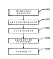
도 3 및 도 5를 참조하면, 하나 이상의 다이들(D)이 픽-앤-플래이스 유닛(2)에 의해 워크피스(W) 상에 배치된 이후, 다이 배치 시스템(14)은 S500에서 워크피스(W) 상의 하나 이상의 다이들(D)의 실제 위치들을 측정한다. 이 예에서, 워크피스(W) 상에 배치된 하나 이상의 다이들(D)은 워크피스(W) 상에 형성될 다중-층 구조의 제 1 층을 구성한다. 3 and 5, after one or more dies D have been placed on the workpiece W by the pick-and-
S502에서, 위치 측정 제어기(4)는 도 1a의 S102에 관하여 위에서 논의된 것과 동일하거나 실질적으로 동일한 방식으로 메모리(20)에 하나 이상의 다이들(D)에 연관되는 위치 데이터를 출력한다. At S502,
S504에서, 영상 기록 제어기(24)는 메모리(20)로부터 실제 위치 데이터를 획득(판독)하고 도 1a의 S104에 관하여 위에서 논의된 바와 같이 메모리(20)로부터 획득된 실제 위치 데이터에 기초하여 패턴 조정 데이터를 생성한다. In S504, the
S506에서, 영상 기록 제어기(24)는 패턴 조정 데이터에 기초하여 수정된 패턴 데이터를 생성한다. 이 예에서, 영상 기록 제어기(24)는 워크피스(W) 상에서 형성되는 다중-층 구조(예를 들어, 도체 패턴 또는 비아 홀 패턴)의 제 2 또는 후속 층에 대한 수정된 패턴 데이터를 생성한다. 이 예에서, 다중-층 구조의 제 1 층은 다중-층 구조의 제 2 층과 상이하다. 수정된 패턴 데이터는 도 1a의 S106에 관하여 위에서 논의된 것과 동일하거나 실질적으로 동일한 방식으로 생성된다. In S506, the
S508에서, 영상 기록기(22)는 수정된 패턴 데이터에 따라 워크피스(W) 상에 패턴을 기록/생성/패터닝함으로써 다중층 구조의 제 2 층을 형성한다. 패턴은 도 1a의 S108에 관하여 위에서 논의된 것과 동일하거나 실질적으로 동일한 방식으로 기록된다. In S508, the
예시적인 실시예들은 2개 이상의 다이들이 서로의 상부 상에 적층되고 제 1 다이의 상부측이 비교적 높은 정렬 정확도로 제 2 다이의 하부측에 연결되는 프로세스에서 활용될 수 있다. 보다 많은 다이들이 이러한 프로세스에서 적층되는 경우, (n-1)번째 다이의 상부는 n-번째 다이의 하부에 연결되며, 여기서 n은 2보다 큰 정수이다. Exemplary embodiments may be utilized in a process in which two or more dies are stacked on top of each other and the top side of the first die is connected to the bottom side of the second die with a relatively high alignment accuracy. If more dies are stacked in this process, the top of the (n−1) th die is connected to the bottom of the n th die, where n is an integer greater than two.
적어도 몇몇 예시적인 실시예들에 따라, 각각의 다이의 위치는 제 1 다이 레벨에서 측정될 수 있고, 측정된 정보는 이어서 제 2 다이 레벨 배치를 수행하는 픽-앤-플래이스 머신에 공급될 수 있어서, 제 1 픽-앤-플래이스 머신 상의 정확도에 대한 요건들을 완화시키고, 이는 결국 상당히 더 높은 속도로 제 1 픽-앤-플래이스 머신이 동작하도록 허용한다. 위에서 언급된 바와 같이, 여기서 기술되는 예시적인 실시예들은 외부 측정 툴을 포함할 필요가 없다. According to at least some example embodiments, the location of each die may be measured at a first die level, and the measured information may then be supplied to a pick-and-place machine performing a second die level placement. Thus mitigating the requirements for accuracy on the first pick-and-place machine, which in turn allows the first pick-and-place machine to operate at significantly higher speeds. As mentioned above, the example embodiments described herein need not include an external measurement tool.
적어도 몇몇 예시적인 실시예들에 따라, 워크피스 상의 다이의 예상되는 위치는 로컬 또는 글로벌 정렬 마크(들)의 위치 및 다이의 로컬 정렬 위치로부터의 입력(예를 들어, 치환, 회전 등)에 기초하여 계산될 수 있다. 워크피스 상의 다이의 실제 위치는 이어서 다이가 워크피스 상에 배치된 직후, 모든 다이들이 워크피스 상에 배치된 이후, 또는 워크피스 상의 다이의 배치 동안 측정될 수 있다. 측정은 또한 픽-앤-플래이스 머신(예를 들어, 접착제의 경화를 위해 또한 이용될 수 있는 유닛이 중간에 배열되는 머신에서)과 함께 별개의 모듈에서 또한 수행될 수 있다.According to at least some example embodiments, the expected position of the die on the workpiece is based on the position of the local or global alignment mark (s) and input from the local alignment position of the die (eg, substitution, rotation, etc.). Can be calculated. The actual position of the die on the workpiece may then be measured immediately after the die is placed on the workpiece, after all the dies are placed on the workpiece, or during placement of the die on the workpiece. The measurement can also be performed in a separate module together with the pick-and-place machine (eg in a machine in which units are arranged in between which can also be used for curing of the adhesive).
예시적인 실시예들의 위의 설명은 예시 및 설명의 목적들을 위해 제공되었다. 이는 소모적이거나 본 개시를 제한하는 것으로 의도되지 않는다. 구체적으로 도시되거나 기술되지 않는 경우 조차도 특정한 실시예의 개별 엘리먼트들 또는 특징들은 일반적으로 그 특정한 예시적인 실시예로 제한되는 것이 아니라, 응용 가능한 경우, 상호 교환 가능하고 선택된 예시적인 실시예에서 이용될 수 있다. 이는 다수의 방식들로 또한 변동될 수 있다. 이러한 변동들은 본 개시로부터 벗어나는 것으로서 간주되지 않고 모든 이러한 수정물들은 본 개시의 범위 내에 포함되도록 의도된다.
The above description of exemplary embodiments has been provided for the purposes of illustration and description. It is not intended to be exhaustive or to limit the disclosure. Even if not specifically shown or described, individual elements or features of a particular embodiment are not generally limited to that particular example embodiment, but can be used in interchangeable and selected example embodiments where applicable. . This can also be varied in a number of ways. Such variations are not to be regarded as a departure from the present disclosure and all such modifications are intended to be included within the scope of the present disclosure.
Claims (16)
상기 워크피스 상의 적어도 하나의 다이의 배치와 상기 워크피스 상의 배치를 위한 후속 다이의 들어 올림(picking up) 간의 시간 동안 적어도 하나의 다이의 실제 위치를 측정 및 검출 중 하나를 하도록 구성되는 다이 위치 결정 유닛
을 포함하는,
장착 헤드.A mounting head of a pick-and-place tool configured to pick and place at least one die on a workpiece,
Die positioning configured to measure and detect the actual position of at least one die during a time between placement of at least one die on the workpiece and picking up of a subsequent die for placement on the workpiece. unit
Including,
Mounting head.
상기 다이 위치 결정 유닛은,
상기 장착 헤드가 상기 워크피스 상의 적어도 하나의 다이를 배치하기 위한 위치에 여전히 있는 동안 상기 적어도 하나의 다이의 실제 위치를 측정 및 검출 중 하나를 하도록 구성되는,
장착 헤드.The method of claim 1,
The die positioning unit,
Configured to measure and detect one of the actual positions of the at least one die while the mounting head is still in position to place at least one die on the workpiece,
Mounting head.
상기 픽-앤-플래이스 툴은,
적어도 하나의 측정 마크에 대해 상기 워크피스 상의 적어도 하나의 다이의 실제 위치를 측정하도록 구성되는,
장착 헤드.The method of claim 1,
The pick-and-place tool,
Configured to measure an actual position of at least one die on the workpiece with respect to at least one measurement mark,
Mounting head.
상기 적어도 하나의 측정 마크는,
상기 워크피스 상의 위치에 연결되거나 연관되는 로컬 정렬 마크 또는 다른 고유한 특징인,
장착 헤드.The method of claim 3, wherein
The at least one measurement mark,
A local alignment mark or other unique feature connected or associated with a location on the workpiece,
Mounting head.
상기 픽-앤-플래이스 툴은,
상기 적어도 하나의 다이의 실제 위치를 나타내는 위치 정보를 출력하도록 구성되고,
상기 위치 정보는,
상기 로컬 정렬 마크 또는 상기 로컬 정렬 마크가 명확히 정의된 거리를 갖는 몇몇 다른 기준 지점에 대한 상기 적어도 하나의 다이의 위치의 측정을 포함하는,
장착 헤드.5. The method of claim 4,
The pick-and-place tool,
Output location information indicating an actual location of the at least one die,
The location information may include:
A measurement of the location of the at least one die relative to the local alignment mark or some other reference point where the local alignment mark has a clearly defined distance,
Mounting head.
상기 픽-앤-플래이스 툴은,
직접적으로 또는 메모리를 통해 간접적으로 측정된 실제 위치를 나타내는 위치 정보를 외부 유닛에 출력하도록 추가로 구성되고,
상기 위치 정보는 상기 워크피스 상에서 생성될 패턴과 연관되는 원래의 패턴 데이터를 조정하는데 유용한,
장착 헤드.The method of claim 3, wherein
The pick-and-place tool,
Is further configured to output position information to an external unit indicating the actual position measured directly or indirectly through a memory,
The position information is useful for adjusting original pattern data associated with a pattern to be generated on the workpiece,
Mounting head.
상기 적어도 하나의 다이 또는 컴포넌트는 제 1 층 상에 배치되고,
상기 패턴 생성기는 상기 제 1 층과 상이한 제 2 층 상에 기록될 원래의 패턴 데이터를 조정하기 위해 상기 위치 정보를 이용하는,
장착 헤드.The method of claim 5, wherein
The at least one die or component is disposed on a first layer,
The pattern generator uses the position information to adjust original pattern data to be recorded on a second layer different from the first layer,
Mounting head.
상기 제 1 층 및 상기 제 2 층은,
배치된 다이들 또는 컴포넌트들의 동일한 그룹과 연관되는 층들인,
장착 헤드.The method of claim 7, wherein
The first layer and the second layer,
Are layers associated with the same group of placed dies or components,
Mounting head.
상기 제 1 층은 배치된 다이들 또는 컴포넌트들의 제 1 그룹과 연관되는 층이고, 제 2 층은 다이들 또는 컴포넌트들의 상기 제 1 그룹과 상이한 배치된 다이들 또는 컴포넌트들의 제 2 그룹과 연관되는 층인,
장착 헤드.The method of claim 7, wherein
The first layer is a layer associated with a first group of disposed dies or components, and the second layer is a layer associated with a second group of deployed dies or components different from the first group of dies or components. ,
Mounting head.
상기 다이 위치 결정 유닛은,
상기 워크피스의 영상을 획득하도록 구성되는 카메라
를 포함하는,
장착 헤드.The method of claim 1,
The die positioning unit,
A camera configured to acquire an image of the workpiece
/ RTI >
Mounting head.
상기 카메라는 전하 결합 디바이스 카메라인,
장착 헤드.11. The method of claim 10,
The camera is a charge coupled device camera,
Mounting head.
상기 다이 위치 결정 유닛은,
상기 워크피스 상의 적어도 하나의 다이의 위치를 검출하도록 구성된 센서
를 포함하는,
장착 헤드.The method of claim 1,
The die positioning unit,
A sensor configured to detect a position of at least one die on the workpiece
/ RTI >
Mounting head.
상기 센서는,
상기 워크피스 상의 적어도 하나의 다이의 위치를 검출하기 위해 반사된 광 및 삼각측량법(triangulation) 중 적어도 하나를 이용하도록 구성되는,
장착 헤드.13. The method of claim 12,
The sensor includes:
Configured to use at least one of reflected light and triangulation to detect a location of at least one die on the workpiece,
Mounting head.
상기 카메라는,
적어도 하나의 측정 마크에 대해 상기 워크피스 상에 배치된 적어도 하나의 다이의 실제 위치를 측정하기 위해 워크피스 표면 영역의 서브영역만만을 커버하는 영상을 획득하도록 구성되는,
장착 헤드.11. The method of claim 10,
The camera comprises:
Configured to acquire an image covering only a subregion of a workpiece surface area to measure the actual position of at least one die disposed on the workpiece for at least one measurement mark,
Mounting head.
상기 카메라에 의해 획득되는 영상은,
단지 상기 워크피스 상에 배치된 복수의 다이들의 서브세트에 대한 실제 위치 정보를 포함하는,
장착 헤드.15. The method of claim 14,
The image obtained by the camera,
Only including actual position information for a subset of the plurality of dies disposed on the workpiece,
Mounting head.
상기 다이들의 서브세트는,
상기 장착 헤드에 의해 수행되는 마지막 픽-앤-플래이스 동작에서 배치되는 적어도 하나의 다이와 동일한,
장착 헤드.The method of claim 15,
The subset of dies is
Same as at least one die disposed in the last pick-and-place operation performed by the mounting head,
Mounting head.
Applications Claiming Priority (3)
| Application Number | Priority Date | Filing Date | Title |
|---|---|---|---|
| US38331710P | 2010-09-15 | 2010-09-15 | |
| US61/383,317 | 2010-09-15 | ||
| PCT/IB2011/002150 WO2012035416A2 (en) | 2010-09-15 | 2011-09-15 | Methods and apparatuses for generating patterns on workpieces |
Publications (2)
| Publication Number | Publication Date |
|---|---|
| KR20130127976A true KR20130127976A (en) | 2013-11-25 |
| KR101819043B1 KR101819043B1 (en) | 2018-01-16 |
Family
ID=44906225
Family Applications (1)
| Application Number | Title | Priority Date | Filing Date |
|---|---|---|---|
| KR1020137009440A KR101819043B1 (en) | 2010-09-15 | 2011-09-15 | Apparatus for generating patterns on workpieces |
Country Status (6)
| Country | Link |
|---|---|
| US (2) | US9032611B2 (en) |
| EP (1) | EP2617053B1 (en) |
| JP (1) | JP6174487B2 (en) |
| KR (1) | KR101819043B1 (en) |
| CN (1) | CN103210483B (en) |
| WO (1) | WO2012035416A2 (en) |
Families Citing this family (22)
| Publication number | Priority date | Publication date | Assignee | Title |
|---|---|---|---|---|
| KR101926423B1 (en) * | 2010-02-26 | 2018-12-07 | 마이크로닉 아베 | Method and apparatus for performing pattern alignment |
| KR101819043B1 (en) * | 2010-09-15 | 2018-01-16 | 마이크로닉 아베 | Apparatus for generating patterns on workpieces |
| JPWO2012169374A1 (en) * | 2011-06-08 | 2015-02-23 | 村田機械株式会社 | Work processing system |
| US9245062B2 (en) | 2012-03-22 | 2016-01-26 | Virtek Vision International Inc. | Laser projection system using variable part alignment |
| TWI570823B (en) | 2013-08-14 | 2017-02-11 | 新川股份有限公司 | Semiconductor manufacturing apparatus and manufacturing method for semiconductor apparatus |
| KR101496059B1 (en) | 2013-12-27 | 2015-02-25 | 세메스 주식회사 | Method of obtaining location information of dies |
| CN104284524B (en) * | 2014-10-27 | 2017-03-22 | 深圳市朝阳光科技有限公司 | LED chip mounter |
| DE102015101759B3 (en) * | 2015-02-06 | 2016-07-07 | Asm Assembly Systems Gmbh & Co. Kg | Picking machine and method for loading a carrier with unhoused chips |
| US9633883B2 (en) | 2015-03-20 | 2017-04-25 | Rohinni, LLC | Apparatus for transfer of semiconductor devices |
| US10692738B2 (en) * | 2015-03-30 | 2020-06-23 | Fuji Corporation | Information management device and information management method |
| CN105489525B (en) * | 2015-12-31 | 2018-12-28 | 广州兴森快捷电路科技有限公司 | Device position indicates system and device position indicating means |
| KR102180449B1 (en) * | 2016-05-13 | 2020-11-19 | 에이에스엠엘 네델란즈 비.브이. | Multiple miniature pickup elements for component stacking and/or pick-and-place processes |
| JP6983229B2 (en) * | 2016-09-13 | 2021-12-17 | ユニバーサル インスツルメンツ コーポレーションUniversal Instruments Corporation | Feeder system, pick and place machine, and method |
| US10504767B2 (en) | 2016-11-23 | 2019-12-10 | Rohinni, LLC | Direct transfer apparatus for a pattern array of semiconductor device die |
| CN109103134B (en) * | 2018-09-01 | 2021-07-30 | 余晓飞 | Chip label streamlined preparation equipment |
| US11094571B2 (en) | 2018-09-28 | 2021-08-17 | Rohinni, LLC | Apparatus to increase transferspeed of semiconductor devices with micro-adjustment |
| JP7369529B2 (en) * | 2019-02-28 | 2023-10-26 | 株式会社オーク製作所 | Exposure equipment and alignment method |
| CN110265526B (en) * | 2019-06-18 | 2020-07-24 | 上海纬而视科技股份有限公司 | A LED packaging process |
| CN112070834B (en) * | 2020-08-11 | 2024-05-10 | 深圳市大族半导体装备科技有限公司 | Compatible multi-chip positioning method, device, equipment and medium |
| US20220367219A1 (en) * | 2021-05-13 | 2022-11-17 | Changxin Memory Technologies, Inc. | Method for adjusting chip mounting position, apparatus, medium, and electronic device |
| CN113689334B (en) * | 2021-08-24 | 2024-12-03 | 深圳市先地图像科技有限公司 | Laser imaging device and laser imaging control method |
| US20230288822A1 (en) * | 2022-03-12 | 2023-09-14 | Applied Materials, Inc. | Package imaging for die location correction in digital lithography |
Family Cites Families (21)
| Publication number | Priority date | Publication date | Assignee | Title |
|---|---|---|---|---|
| JPH08162797A (en) | 1994-12-08 | 1996-06-21 | Matsushita Electric Ind Co Ltd | Electronic part mounter |
| JPH10145094A (en) * | 1996-11-14 | 1998-05-29 | Nec Corp | Parts mounting device |
| JPH1144508A (en) * | 1997-07-24 | 1999-02-16 | Genichi Tagata | Component mounting method and device |
| JPH11330798A (en) * | 1998-05-19 | 1999-11-30 | Fuji Mach Mfg Co Ltd | Method for mounting electric component and system thereof |
| JP2000340584A (en) * | 1999-05-26 | 2000-12-08 | Toshiba Corp | Chip-mounting method and device |
| US6165658A (en) * | 1999-07-06 | 2000-12-26 | Creo Ltd. | Nonlinear image distortion correction in printed circuit board manufacturing |
| US6537400B1 (en) | 2000-03-06 | 2003-03-25 | Micron Technology, Inc. | Automated method of attaching flip chip devices to a substrate |
| JP2001332677A (en) * | 2000-05-25 | 2001-11-30 | Sony Corp | Method for manufacturing semiconductor device |
| US7058474B2 (en) | 2000-11-08 | 2006-06-06 | Orbotech Ltd. | Multi-layer printed circuit board fabrication system and method |
| KR100983748B1 (en) * | 2002-05-02 | 2010-09-24 | 오르보테크 엘티디. | System and method for manufacturing printed circuit boards using non-uniformly modified images |
| US6974168B2 (en) * | 2002-09-30 | 2005-12-13 | Intel Corporation | System and method for performing simultaneous precision die bond of photonic components onto a single substrate |
| JP4494922B2 (en) * | 2004-10-07 | 2010-06-30 | Juki株式会社 | Method and apparatus for detecting mounting error of electronic component mounting apparatus |
| JP4587861B2 (en) * | 2005-04-05 | 2010-11-24 | Juki株式会社 | Component mounting device |
| JP2007199225A (en) * | 2006-01-25 | 2007-08-09 | Cmk Corp | Exposure system and method for manufacturing printed wiring board with built-in components |
| CN101459102B (en) * | 2007-12-13 | 2010-08-11 | 中芯国际集成电路制造(上海)有限公司 | Wafer positioning method |
| JP5205189B2 (en) * | 2008-09-16 | 2013-06-05 | ルネサスエレクトロニクス株式会社 | Manufacturing method of semiconductor device |
| CN102742378A (en) | 2009-12-30 | 2012-10-17 | 麦戴塔自动控制股份公司 | A component mounting machine |
| KR101926423B1 (en) | 2010-02-26 | 2018-12-07 | 마이크로닉 아베 | Method and apparatus for performing pattern alignment |
| US8934081B2 (en) | 2010-03-01 | 2015-01-13 | Mycronic AB | Method and apparatus for performing alignment using reference board |
| US8372666B2 (en) * | 2010-07-06 | 2013-02-12 | Intel Corporation | Misalignment correction for embedded microelectronic die applications |
| KR101819043B1 (en) * | 2010-09-15 | 2018-01-16 | 마이크로닉 아베 | Apparatus for generating patterns on workpieces |
-
2011
- 2011-09-15 KR KR1020137009440A patent/KR101819043B1/en active IP Right Grant
- 2011-09-15 US US13/233,649 patent/US9032611B2/en active Active
- 2011-09-15 CN CN201180054889.6A patent/CN103210483B/en active Active
- 2011-09-15 JP JP2013528781A patent/JP6174487B2/en active Active
- 2011-09-15 EP EP11778668.1A patent/EP2617053B1/en active Active
- 2011-09-15 WO PCT/IB2011/002150 patent/WO2012035416A2/en active Application Filing
-
2014
- 2014-12-02 US US14/557,952 patent/US9648795B2/en active Active
Also Published As
| Publication number | Publication date |
|---|---|
| KR101819043B1 (en) | 2018-01-16 |
| CN103210483B (en) | 2016-06-29 |
| EP2617053B1 (en) | 2014-11-12 |
| JP2013545259A (en) | 2013-12-19 |
| US9648795B2 (en) | 2017-05-09 |
| US20150082620A1 (en) | 2015-03-26 |
| WO2012035416A3 (en) | 2012-05-10 |
| CN103210483A (en) | 2013-07-17 |
| EP2617053A2 (en) | 2013-07-24 |
| JP6174487B2 (en) | 2017-08-02 |
| US20120066898A1 (en) | 2012-03-22 |
| WO2012035416A2 (en) | 2012-03-22 |
| US9032611B2 (en) | 2015-05-19 |
Similar Documents
| Publication | Publication Date | Title |
|---|---|---|
| KR101819043B1 (en) | Apparatus for generating patterns on workpieces | |
| US9341962B2 (en) | Method and apparatus for performing pattern alignment to die | |
| JP5637771B2 (en) | Direct drawing method and direct drawing apparatus | |
| KR20140001741A (en) | Generating apparatus of wiring data, generating method, and drawing apparatus | |
| TWI617932B (en) | Apparatus for and method of generating wiring data, and imaging system | |
| JP2009054759A (en) | Anomaly detection method and apparatus | |
| JP4515814B2 (en) | Mounting accuracy measurement method | |
| JP6264760B2 (en) | Mounting method and mounting apparatus | |
| CN114613713A (en) | Semiconductor manufacturing apparatus, position reading method, and attaching method | |
| US20050084778A1 (en) | Reticle alignment procedure | |
| JP5108594B2 (en) | Tape carrier, semiconductor device, and misalignment determination method |
Legal Events
| Date | Code | Title | Description |
|---|---|---|---|
| PA0105 | International application |
Patent event date: 20130412 Patent event code: PA01051R01D Comment text: International Patent Application |
|
| PG1501 | Laying open of application | ||
| PA0201 | Request for examination |
Patent event code: PA02012R01D Patent event date: 20160422 Comment text: Request for Examination of Application |
|
| E902 | Notification of reason for refusal | ||
| PE0902 | Notice of grounds for rejection |
Comment text: Notification of reason for refusal Patent event date: 20161020 Patent event code: PE09021S01D |
|
| E902 | Notification of reason for refusal | ||
| PE0902 | Notice of grounds for rejection |
Comment text: Notification of reason for refusal Patent event date: 20170427 Patent event code: PE09021S01D |
|
| E701 | Decision to grant or registration of patent right | ||
| PE0701 | Decision of registration |
Patent event code: PE07011S01D Comment text: Decision to Grant Registration Patent event date: 20171102 |
|
| GRNT | Written decision to grant | ||
| PR0701 | Registration of establishment |
Comment text: Registration of Establishment Patent event date: 20180110 Patent event code: PR07011E01D |
|
| PR1002 | Payment of registration fee |
Payment date: 20180111 End annual number: 3 Start annual number: 1 |
|
| PG1601 | Publication of registration | ||
| PR1001 | Payment of annual fee |
Payment date: 20210104 Start annual number: 4 End annual number: 4 |
|
| PR1001 | Payment of annual fee |
Payment date: 20211221 Start annual number: 5 End annual number: 5 |
|
| PR1001 | Payment of annual fee |
Payment date: 20231227 Start annual number: 7 End annual number: 7 |
|
| PR1001 | Payment of annual fee |
Payment date: 20241224 Start annual number: 8 End annual number: 8 |