KR20130061678A - Power source circuit - Google Patents
Power source circuit Download PDFInfo
- Publication number
- KR20130061678A KR20130061678A KR1020127028567A KR20127028567A KR20130061678A KR 20130061678 A KR20130061678 A KR 20130061678A KR 1020127028567 A KR1020127028567 A KR 1020127028567A KR 20127028567 A KR20127028567 A KR 20127028567A KR 20130061678 A KR20130061678 A KR 20130061678A
- Authority
- KR
- South Korea
- Prior art keywords
- terminal
- transistor
- circuit
- oxide semiconductor
- semiconductor film
- Prior art date
- Legal status (The legal status is an assumption and is not a legal conclusion. Google has not performed a legal analysis and makes no representation as to the accuracy of the status listed.)
- Ceased
Links
- 238000012935 Averaging Methods 0.000 claims abstract description 20
- 238000009499 grossing Methods 0.000 claims abstract description 14
- 239000004065 semiconductor Substances 0.000 claims description 157
- 238000000034 method Methods 0.000 claims description 76
- 230000015572 biosynthetic process Effects 0.000 claims description 34
- 230000015556 catabolic process Effects 0.000 abstract description 11
- 238000006731 degradation reaction Methods 0.000 abstract description 3
- 239000010408 film Substances 0.000 description 235
- 239000010410 layer Substances 0.000 description 88
- 239000000758 substrate Substances 0.000 description 43
- 238000004544 sputter deposition Methods 0.000 description 38
- 239000007789 gas Substances 0.000 description 30
- 238000010438 heat treatment Methods 0.000 description 30
- 230000008569 process Effects 0.000 description 29
- XKRFYHLGVUSROY-UHFFFAOYSA-N Argon Chemical compound [Ar] XKRFYHLGVUSROY-UHFFFAOYSA-N 0.000 description 26
- 239000000463 material Substances 0.000 description 24
- QVGXLLKOCUKJST-UHFFFAOYSA-N atomic oxygen Chemical compound [O] QVGXLLKOCUKJST-UHFFFAOYSA-N 0.000 description 23
- 239000001301 oxygen Substances 0.000 description 23
- 229910052760 oxygen Inorganic materials 0.000 description 23
- 239000001257 hydrogen Substances 0.000 description 22
- 229910052739 hydrogen Inorganic materials 0.000 description 22
- VYPSYNLAJGMNEJ-UHFFFAOYSA-N silicon dioxide Inorganic materials O=[Si]=O VYPSYNLAJGMNEJ-UHFFFAOYSA-N 0.000 description 22
- 238000005530 etching Methods 0.000 description 20
- 229910052710 silicon Inorganic materials 0.000 description 19
- XUIMIQQOPSSXEZ-UHFFFAOYSA-N Silicon Chemical compound [Si] XUIMIQQOPSSXEZ-UHFFFAOYSA-N 0.000 description 18
- 239000010703 silicon Substances 0.000 description 18
- 229910052814 silicon oxide Inorganic materials 0.000 description 16
- 239000012298 atmosphere Substances 0.000 description 15
- 230000002829 reductive effect Effects 0.000 description 15
- XLYOFNOQVPJJNP-UHFFFAOYSA-N water Substances O XLYOFNOQVPJJNP-UHFFFAOYSA-N 0.000 description 14
- 229910001868 water Inorganic materials 0.000 description 14
- UFHFLCQGNIYNRP-UHFFFAOYSA-N Hydrogen Chemical compound [H][H] UFHFLCQGNIYNRP-UHFFFAOYSA-N 0.000 description 13
- 229910052782 aluminium Inorganic materials 0.000 description 13
- 229910052786 argon Inorganic materials 0.000 description 13
- 239000010936 titanium Substances 0.000 description 13
- XLOMVQKBTHCTTD-UHFFFAOYSA-N Zinc monoxide Chemical compound [Zn]=O XLOMVQKBTHCTTD-UHFFFAOYSA-N 0.000 description 12
- 238000010586 diagram Methods 0.000 description 12
- 229910044991 metal oxide Inorganic materials 0.000 description 12
- 150000004706 metal oxides Chemical class 0.000 description 12
- 230000001681 protective effect Effects 0.000 description 12
- IJGRMHOSHXDMSA-UHFFFAOYSA-N Atomic nitrogen Chemical compound N#N IJGRMHOSHXDMSA-UHFFFAOYSA-N 0.000 description 11
- 229910007541 Zn O Inorganic materials 0.000 description 11
- 230000006866 deterioration Effects 0.000 description 11
- 229910052719 titanium Inorganic materials 0.000 description 11
- 229910052581 Si3N4 Inorganic materials 0.000 description 10
- 239000012535 impurity Substances 0.000 description 10
- HQVNEWCFYHHQES-UHFFFAOYSA-N silicon nitride Chemical compound N12[Si]34N5[Si]62N3[Si]51N64 HQVNEWCFYHHQES-UHFFFAOYSA-N 0.000 description 10
- XAGFODPZIPBFFR-UHFFFAOYSA-N aluminium Chemical compound [Al] XAGFODPZIPBFFR-UHFFFAOYSA-N 0.000 description 9
- 238000006243 chemical reaction Methods 0.000 description 9
- 150000002431 hydrogen Chemical class 0.000 description 9
- 238000000206 photolithography Methods 0.000 description 9
- RTAQQCXQSZGOHL-UHFFFAOYSA-N Titanium Chemical compound [Ti] RTAQQCXQSZGOHL-UHFFFAOYSA-N 0.000 description 8
- 229910052751 metal Inorganic materials 0.000 description 8
- 125000004435 hydrogen atom Chemical group [H]* 0.000 description 7
- 229910052750 molybdenum Inorganic materials 0.000 description 7
- QTBSBXVTEAMEQO-UHFFFAOYSA-N Acetic acid Chemical compound CC(O)=O QTBSBXVTEAMEQO-UHFFFAOYSA-N 0.000 description 6
- 125000002887 hydroxy group Chemical group [H]O* 0.000 description 6
- 239000007788 liquid Substances 0.000 description 6
- 238000004519 manufacturing process Methods 0.000 description 6
- 239000012071 phase Substances 0.000 description 6
- 239000010453 quartz Substances 0.000 description 6
- 239000002356 single layer Substances 0.000 description 6
- 229910052721 tungsten Inorganic materials 0.000 description 6
- 239000011787 zinc oxide Substances 0.000 description 6
- 239000000956 alloy Substances 0.000 description 5
- 150000001875 compounds Chemical class 0.000 description 5
- 229910052802 copper Inorganic materials 0.000 description 5
- 239000010949 copper Substances 0.000 description 5
- 229910052757 nitrogen Inorganic materials 0.000 description 5
- 101000685663 Homo sapiens Sodium/nucleoside cotransporter 1 Proteins 0.000 description 4
- 101000821827 Homo sapiens Sodium/nucleoside cotransporter 2 Proteins 0.000 description 4
- 101000822028 Homo sapiens Solute carrier family 28 member 3 Proteins 0.000 description 4
- ZOKXTWBITQBERF-UHFFFAOYSA-N Molybdenum Chemical compound [Mo] ZOKXTWBITQBERF-UHFFFAOYSA-N 0.000 description 4
- NBIIXXVUZAFLBC-UHFFFAOYSA-N Phosphoric acid Chemical compound OP(O)(O)=O NBIIXXVUZAFLBC-UHFFFAOYSA-N 0.000 description 4
- 102100023116 Sodium/nucleoside cotransporter 1 Human genes 0.000 description 4
- 102100021541 Sodium/nucleoside cotransporter 2 Human genes 0.000 description 4
- 102100021470 Solute carrier family 28 member 3 Human genes 0.000 description 4
- 229910045601 alloy Inorganic materials 0.000 description 4
- 239000000460 chlorine Substances 0.000 description 4
- 229910052804 chromium Inorganic materials 0.000 description 4
- 239000011651 chromium Substances 0.000 description 4
- KPUWHANPEXNPJT-UHFFFAOYSA-N disiloxane Chemical class [SiH3]O[SiH3] KPUWHANPEXNPJT-UHFFFAOYSA-N 0.000 description 4
- 229910052733 gallium Inorganic materials 0.000 description 4
- 150000004678 hydrides Chemical class 0.000 description 4
- 239000011261 inert gas Substances 0.000 description 4
- 238000002347 injection Methods 0.000 description 4
- 239000007924 injection Substances 0.000 description 4
- 239000002184 metal Substances 0.000 description 4
- 239000011733 molybdenum Substances 0.000 description 4
- TWNQGVIAIRXVLR-UHFFFAOYSA-N oxo(oxoalumanyloxy)alumane Chemical compound O=[Al]O[Al]=O TWNQGVIAIRXVLR-UHFFFAOYSA-N 0.000 description 4
- 238000001552 radio frequency sputter deposition Methods 0.000 description 4
- 238000004151 rapid thermal annealing Methods 0.000 description 4
- 239000011347 resin Substances 0.000 description 4
- 229920005989 resin Polymers 0.000 description 4
- HBMJWWWQQXIZIP-UHFFFAOYSA-N silicon carbide Chemical compound [Si+]#[C-] HBMJWWWQQXIZIP-UHFFFAOYSA-N 0.000 description 4
- 229910010271 silicon carbide Inorganic materials 0.000 description 4
- 239000000243 solution Substances 0.000 description 4
- 229910052715 tantalum Inorganic materials 0.000 description 4
- 238000001039 wet etching Methods 0.000 description 4
- ZAMOUSCENKQFHK-UHFFFAOYSA-N Chlorine atom Chemical compound [Cl] ZAMOUSCENKQFHK-UHFFFAOYSA-N 0.000 description 3
- RYGMFSIKBFXOCR-UHFFFAOYSA-N Copper Chemical compound [Cu] RYGMFSIKBFXOCR-UHFFFAOYSA-N 0.000 description 3
- MYMOFIZGZYHOMD-UHFFFAOYSA-N Dioxygen Chemical compound O=O MYMOFIZGZYHOMD-UHFFFAOYSA-N 0.000 description 3
- 229910005191 Ga 2 O 3 Inorganic materials 0.000 description 3
- MHAJPDPJQMAIIY-UHFFFAOYSA-N Hydrogen peroxide Chemical compound OO MHAJPDPJQMAIIY-UHFFFAOYSA-N 0.000 description 3
- 229910019092 Mg-O Inorganic materials 0.000 description 3
- 229910019395 Mg—O Inorganic materials 0.000 description 3
- NRTOMJZYCJJWKI-UHFFFAOYSA-N Titanium nitride Chemical compound [Ti]#N NRTOMJZYCJJWKI-UHFFFAOYSA-N 0.000 description 3
- 239000000654 additive Substances 0.000 description 3
- 230000000996 additive effect Effects 0.000 description 3
- QGZKDVFQNNGYKY-UHFFFAOYSA-N ammonia Natural products N QGZKDVFQNNGYKY-UHFFFAOYSA-N 0.000 description 3
- 230000004888 barrier function Effects 0.000 description 3
- 239000003990 capacitor Substances 0.000 description 3
- 229910052801 chlorine Inorganic materials 0.000 description 3
- 238000000151 deposition Methods 0.000 description 3
- 230000008021 deposition Effects 0.000 description 3
- 229910001882 dioxygen Inorganic materials 0.000 description 3
- 238000001312 dry etching Methods 0.000 description 3
- 239000011521 glass Substances 0.000 description 3
- 239000001307 helium Substances 0.000 description 3
- 229910052734 helium Inorganic materials 0.000 description 3
- SWQJXJOGLNCZEY-UHFFFAOYSA-N helium atom Chemical compound [He] SWQJXJOGLNCZEY-UHFFFAOYSA-N 0.000 description 3
- 239000007769 metal material Substances 0.000 description 3
- 239000000203 mixture Substances 0.000 description 3
- 238000005268 plasma chemical vapour deposition Methods 0.000 description 3
- 239000010937 tungsten Substances 0.000 description 3
- YCKRFDGAMUMZLT-UHFFFAOYSA-N Fluorine atom Chemical compound [F] YCKRFDGAMUMZLT-UHFFFAOYSA-N 0.000 description 2
- XPDWGBQVDMORPB-UHFFFAOYSA-N Fluoroform Chemical compound FC(F)F XPDWGBQVDMORPB-UHFFFAOYSA-N 0.000 description 2
- 229910002601 GaN Inorganic materials 0.000 description 2
- JMASRVWKEDWRBT-UHFFFAOYSA-N Gallium nitride Chemical compound [Ga]#N JMASRVWKEDWRBT-UHFFFAOYSA-N 0.000 description 2
- 108010083687 Ion Pumps Proteins 0.000 description 2
- 229910052779 Neodymium Inorganic materials 0.000 description 2
- GRYLNZFGIOXLOG-UHFFFAOYSA-N Nitric acid Chemical compound O[N+]([O-])=O GRYLNZFGIOXLOG-UHFFFAOYSA-N 0.000 description 2
- 229910006404 SnO 2 Inorganic materials 0.000 description 2
- 230000002411 adverse Effects 0.000 description 2
- 229910000147 aluminium phosphate Inorganic materials 0.000 description 2
- 239000012300 argon atmosphere Substances 0.000 description 2
- SWXQKHHHCFXQJF-UHFFFAOYSA-N azane;hydrogen peroxide Chemical compound [NH4+].[O-]O SWXQKHHHCFXQJF-UHFFFAOYSA-N 0.000 description 2
- 239000005380 borophosphosilicate glass Substances 0.000 description 2
- PMHQVHHXPFUNSP-UHFFFAOYSA-M copper(1+);methylsulfanylmethane;bromide Chemical compound Br[Cu].CSC PMHQVHHXPFUNSP-UHFFFAOYSA-M 0.000 description 2
- 238000002425 crystallisation Methods 0.000 description 2
- 230000008025 crystallization Effects 0.000 description 2
- 239000000428 dust Substances 0.000 description 2
- 238000011049 filling Methods 0.000 description 2
- 238000007667 floating Methods 0.000 description 2
- 229910052731 fluorine Inorganic materials 0.000 description 2
- 239000011737 fluorine Substances 0.000 description 2
- 125000001153 fluoro group Chemical group F* 0.000 description 2
- 229910052738 indium Inorganic materials 0.000 description 2
- 238000009434 installation Methods 0.000 description 2
- 230000010354 integration Effects 0.000 description 2
- 229910052748 manganese Inorganic materials 0.000 description 2
- 229910017604 nitric acid Inorganic materials 0.000 description 2
- 150000004767 nitrides Chemical class 0.000 description 2
- 239000012299 nitrogen atmosphere Substances 0.000 description 2
- 125000000962 organic group Chemical group 0.000 description 2
- 239000011368 organic material Substances 0.000 description 2
- 239000005360 phosphosilicate glass Substances 0.000 description 2
- 238000001020 plasma etching Methods 0.000 description 2
- 230000005855 radiation Effects 0.000 description 2
- 230000004044 response Effects 0.000 description 2
- 230000002441 reversible effect Effects 0.000 description 2
- 229910052706 scandium Inorganic materials 0.000 description 2
- 238000000859 sublimation Methods 0.000 description 2
- 230000008022 sublimation Effects 0.000 description 2
- 239000000126 substance Substances 0.000 description 2
- VZGDMQKNWNREIO-UHFFFAOYSA-N tetrachloromethane Chemical compound ClC(Cl)(Cl)Cl VZGDMQKNWNREIO-UHFFFAOYSA-N 0.000 description 2
- 239000010409 thin film Substances 0.000 description 2
- WFKWXMTUELFFGS-UHFFFAOYSA-N tungsten Chemical compound [W] WFKWXMTUELFFGS-UHFFFAOYSA-N 0.000 description 2
- 239000002699 waste material Substances 0.000 description 2
- VXEGSRKPIUDPQT-UHFFFAOYSA-N 4-[4-(4-methoxyphenyl)piperazin-1-yl]aniline Chemical compound C1=CC(OC)=CC=C1N1CCN(C=2C=CC(N)=CC=2)CC1 VXEGSRKPIUDPQT-UHFFFAOYSA-N 0.000 description 1
- VHUUQVKOLVNVRT-UHFFFAOYSA-N Ammonium hydroxide Chemical compound [NH4+].[OH-] VHUUQVKOLVNVRT-UHFFFAOYSA-N 0.000 description 1
- OKTJSMMVPCPJKN-UHFFFAOYSA-N Carbon Chemical compound [C] OKTJSMMVPCPJKN-UHFFFAOYSA-N 0.000 description 1
- VYZAMTAEIAYCRO-UHFFFAOYSA-N Chromium Chemical compound [Cr] VYZAMTAEIAYCRO-UHFFFAOYSA-N 0.000 description 1
- 239000004593 Epoxy Substances 0.000 description 1
- CPELXLSAUQHCOX-UHFFFAOYSA-N Hydrogen bromide Chemical compound Br CPELXLSAUQHCOX-UHFFFAOYSA-N 0.000 description 1
- 206010021143 Hypoxia Diseases 0.000 description 1
- DGAQECJNVWCQMB-PUAWFVPOSA-M Ilexoside XXIX Chemical compound C[C@@H]1CC[C@@]2(CC[C@@]3(C(=CC[C@H]4[C@]3(CC[C@@H]5[C@@]4(CC[C@@H](C5(C)C)OS(=O)(=O)[O-])C)C)[C@@H]2[C@]1(C)O)C)C(=O)O[C@H]6[C@@H]([C@H]([C@@H]([C@H](O6)CO)O)O)O.[Na+] DGAQECJNVWCQMB-PUAWFVPOSA-M 0.000 description 1
- 239000004952 Polyamide Substances 0.000 description 1
- 239000004642 Polyimide Substances 0.000 description 1
- 229910018503 SF6 Inorganic materials 0.000 description 1
- 229910003902 SiCl 4 Inorganic materials 0.000 description 1
- 229910002808 Si–O–Si Inorganic materials 0.000 description 1
- 229910020833 Sn-Al-Zn Inorganic materials 0.000 description 1
- 229910020923 Sn-O Inorganic materials 0.000 description 1
- AZWHFTKIBIQKCA-UHFFFAOYSA-N [Sn+2]=O.[O-2].[In+3] Chemical compound [Sn+2]=O.[O-2].[In+3] AZWHFTKIBIQKCA-UHFFFAOYSA-N 0.000 description 1
- NIXOWILDQLNWCW-UHFFFAOYSA-N acrylic acid group Chemical group C(C=C)(=O)O NIXOWILDQLNWCW-UHFFFAOYSA-N 0.000 description 1
- 125000000217 alkyl group Chemical group 0.000 description 1
- 238000005275 alloying Methods 0.000 description 1
- 239000005407 aluminoborosilicate glass Substances 0.000 description 1
- 239000005354 aluminosilicate glass Substances 0.000 description 1
- 229910021529 ammonia Inorganic materials 0.000 description 1
- 230000003321 amplification Effects 0.000 description 1
- 125000003118 aryl group Chemical group 0.000 description 1
- 229910052788 barium Inorganic materials 0.000 description 1
- DSAJWYNOEDNPEQ-UHFFFAOYSA-N barium atom Chemical compound [Ba] DSAJWYNOEDNPEQ-UHFFFAOYSA-N 0.000 description 1
- UMIVXZPTRXBADB-UHFFFAOYSA-N benzocyclobutene Chemical compound C1=CC=C2CCC2=C1 UMIVXZPTRXBADB-UHFFFAOYSA-N 0.000 description 1
- 239000005388 borosilicate glass Substances 0.000 description 1
- 229910052799 carbon Inorganic materials 0.000 description 1
- 125000004432 carbon atom Chemical group C* 0.000 description 1
- 239000000919 ceramic Substances 0.000 description 1
- 230000008859 change Effects 0.000 description 1
- 230000018044 dehydration Effects 0.000 description 1
- 238000006297 dehydration reaction Methods 0.000 description 1
- 238000006356 dehydrogenation reaction Methods 0.000 description 1
- 229910001873 dinitrogen Inorganic materials 0.000 description 1
- 238000007598 dipping method Methods 0.000 description 1
- 230000000694 effects Effects 0.000 description 1
- 230000005669 field effect Effects 0.000 description 1
- 229910052736 halogen Inorganic materials 0.000 description 1
- 150000002367 halogens Chemical class 0.000 description 1
- 239000002784 hot electron Substances 0.000 description 1
- XLYOFNOQVPJJNP-UHFFFAOYSA-M hydroxide Chemical compound [OH-] XLYOFNOQVPJJNP-UHFFFAOYSA-M 0.000 description 1
- APFVFJFRJDLVQX-UHFFFAOYSA-N indium atom Chemical compound [In] APFVFJFRJDLVQX-UHFFFAOYSA-N 0.000 description 1
- 229910003437 indium oxide Inorganic materials 0.000 description 1
- PJXISJQVUVHSOJ-UHFFFAOYSA-N indium(iii) oxide Chemical compound [O-2].[O-2].[O-2].[In+3].[In+3] PJXISJQVUVHSOJ-UHFFFAOYSA-N 0.000 description 1
- 238000009616 inductively coupled plasma Methods 0.000 description 1
- 229910010272 inorganic material Inorganic materials 0.000 description 1
- 239000011147 inorganic material Substances 0.000 description 1
- 238000010030 laminating Methods 0.000 description 1
- 230000000670 limiting effect Effects 0.000 description 1
- 238000001755 magnetron sputter deposition Methods 0.000 description 1
- 230000007246 mechanism Effects 0.000 description 1
- 230000008018 melting Effects 0.000 description 1
- 238000002844 melting Methods 0.000 description 1
- QSHDDOUJBYECFT-UHFFFAOYSA-N mercury Chemical compound [Hg] QSHDDOUJBYECFT-UHFFFAOYSA-N 0.000 description 1
- 229910052753 mercury Inorganic materials 0.000 description 1
- 229910001507 metal halide Inorganic materials 0.000 description 1
- 150000005309 metal halides Chemical class 0.000 description 1
- 150000002739 metals Chemical class 0.000 description 1
- 239000013081 microcrystal Substances 0.000 description 1
- QKCGXXHCELUCKW-UHFFFAOYSA-N n-[4-[4-(dinaphthalen-2-ylamino)phenyl]phenyl]-n-naphthalen-2-ylnaphthalen-2-amine Chemical compound C1=CC=CC2=CC(N(C=3C=CC(=CC=3)C=3C=CC(=CC=3)N(C=3C=C4C=CC=CC4=CC=3)C=3C=C4C=CC=CC4=CC=3)C3=CC4=CC=CC=C4C=C3)=CC=C21 QKCGXXHCELUCKW-UHFFFAOYSA-N 0.000 description 1
- QEFYFXOXNSNQGX-UHFFFAOYSA-N neodymium atom Chemical compound [Nd] QEFYFXOXNSNQGX-UHFFFAOYSA-N 0.000 description 1
- 229910052754 neon Inorganic materials 0.000 description 1
- GKAOGPIIYCISHV-UHFFFAOYSA-N neon atom Chemical compound [Ne] GKAOGPIIYCISHV-UHFFFAOYSA-N 0.000 description 1
- 238000003199 nucleic acid amplification method Methods 0.000 description 1
- 238000007645 offset printing Methods 0.000 description 1
- 239000002245 particle Substances 0.000 description 1
- 238000002161 passivation Methods 0.000 description 1
- 238000009832 plasma treatment Methods 0.000 description 1
- 239000004033 plastic Substances 0.000 description 1
- 229920002647 polyamide Polymers 0.000 description 1
- 229920001721 polyimide Polymers 0.000 description 1
- 238000005546 reactive sputtering Methods 0.000 description 1
- 229910052594 sapphire Inorganic materials 0.000 description 1
- 239000010980 sapphire Substances 0.000 description 1
- SIXSYDAISGFNSX-UHFFFAOYSA-N scandium atom Chemical compound [Sc] SIXSYDAISGFNSX-UHFFFAOYSA-N 0.000 description 1
- 238000007650 screen-printing Methods 0.000 description 1
- LIVNPJMFVYWSIS-UHFFFAOYSA-N silicon monoxide Chemical compound [Si-]#[O+] LIVNPJMFVYWSIS-UHFFFAOYSA-N 0.000 description 1
- 239000005049 silicon tetrachloride Substances 0.000 description 1
- 239000011734 sodium Substances 0.000 description 1
- 229910052708 sodium Inorganic materials 0.000 description 1
- 238000001179 sorption measurement Methods 0.000 description 1
- 238000004528 spin coating Methods 0.000 description 1
- 238000005507 spraying Methods 0.000 description 1
- 239000007858 starting material Substances 0.000 description 1
- 125000001424 substituent group Chemical group 0.000 description 1
- SFZCNBIFKDRMGX-UHFFFAOYSA-N sulfur hexafluoride Chemical compound FS(F)(F)(F)(F)F SFZCNBIFKDRMGX-UHFFFAOYSA-N 0.000 description 1
- 229960000909 sulfur hexafluoride Drugs 0.000 description 1
- GUVRBAGPIYLISA-UHFFFAOYSA-N tantalum atom Chemical compound [Ta] GUVRBAGPIYLISA-UHFFFAOYSA-N 0.000 description 1
- MZLGASXMSKOWSE-UHFFFAOYSA-N tantalum nitride Chemical compound [Ta]#N MZLGASXMSKOWSE-UHFFFAOYSA-N 0.000 description 1
- 239000013076 target substance Substances 0.000 description 1
- TXEYQDLBPFQVAA-UHFFFAOYSA-N tetrafluoromethane Chemical compound FC(F)(F)F TXEYQDLBPFQVAA-UHFFFAOYSA-N 0.000 description 1
- 238000002230 thermal chemical vapour deposition Methods 0.000 description 1
- XOLBLPGZBRYERU-UHFFFAOYSA-N tin dioxide Chemical compound O=[Sn]=O XOLBLPGZBRYERU-UHFFFAOYSA-N 0.000 description 1
- 229910001887 tin oxide Inorganic materials 0.000 description 1
- FAQYAMRNWDIXMY-UHFFFAOYSA-N trichloroborane Chemical compound ClB(Cl)Cl FAQYAMRNWDIXMY-UHFFFAOYSA-N 0.000 description 1
- -1 tungsten nitride Chemical class 0.000 description 1
- 238000007738 vacuum evaporation Methods 0.000 description 1
- 238000001947 vapour-phase growth Methods 0.000 description 1
- 238000005406 washing Methods 0.000 description 1
- 229910052724 xenon Inorganic materials 0.000 description 1
- FHNFHKCVQCLJFQ-UHFFFAOYSA-N xenon atom Chemical compound [Xe] FHNFHKCVQCLJFQ-UHFFFAOYSA-N 0.000 description 1
- 229910052725 zinc Inorganic materials 0.000 description 1
- 239000011701 zinc Substances 0.000 description 1
- OYQCBJZGELKKPM-UHFFFAOYSA-N zinc indium(3+) oxygen(2-) Chemical compound [O-2].[Zn+2].[O-2].[In+3] OYQCBJZGELKKPM-UHFFFAOYSA-N 0.000 description 1
Images


Classifications
-
- H—ELECTRICITY
- H02—GENERATION; CONVERSION OR DISTRIBUTION OF ELECTRIC POWER
- H02M—APPARATUS FOR CONVERSION BETWEEN AC AND AC, BETWEEN AC AND DC, OR BETWEEN DC AND DC, AND FOR USE WITH MAINS OR SIMILAR POWER SUPPLY SYSTEMS; CONVERSION OF DC OR AC INPUT POWER INTO SURGE OUTPUT POWER; CONTROL OR REGULATION THEREOF
- H02M3/00—Conversion of DC power input into DC power output
- H02M3/02—Conversion of DC power input into DC power output without intermediate conversion into AC
- H02M3/04—Conversion of DC power input into DC power output without intermediate conversion into AC by static converters
- H02M3/10—Conversion of DC power input into DC power output without intermediate conversion into AC by static converters using discharge tubes with control electrode or semiconductor devices with control electrode
- H02M3/145—Conversion of DC power input into DC power output without intermediate conversion into AC by static converters using discharge tubes with control electrode or semiconductor devices with control electrode using devices of a triode or transistor type requiring continuous application of a control signal
- H02M3/155—Conversion of DC power input into DC power output without intermediate conversion into AC by static converters using discharge tubes with control electrode or semiconductor devices with control electrode using devices of a triode or transistor type requiring continuous application of a control signal using semiconductor devices only
- H02M3/156—Conversion of DC power input into DC power output without intermediate conversion into AC by static converters using discharge tubes with control electrode or semiconductor devices with control electrode using devices of a triode or transistor type requiring continuous application of a control signal using semiconductor devices only with automatic control of output voltage or current, e.g. switching regulators
- H02M3/157—Conversion of DC power input into DC power output without intermediate conversion into AC by static converters using discharge tubes with control electrode or semiconductor devices with control electrode using devices of a triode or transistor type requiring continuous application of a control signal using semiconductor devices only with automatic control of output voltage or current, e.g. switching regulators with digital control
-
- G—PHYSICS
- G05—CONTROLLING; REGULATING
- G05F—SYSTEMS FOR REGULATING ELECTRIC OR MAGNETIC VARIABLES
- G05F1/00—Automatic systems in which deviations of an electric quantity from one or more predetermined values are detected at the output of the system and fed back to a device within the system to restore the detected quantity to its predetermined value or values, i.e. retroactive systems
-
- G—PHYSICS
- G09—EDUCATION; CRYPTOGRAPHY; DISPLAY; ADVERTISING; SEALS
- G09G—ARRANGEMENTS OR CIRCUITS FOR CONTROL OF INDICATING DEVICES USING STATIC MEANS TO PRESENT VARIABLE INFORMATION
- G09G3/00—Control arrangements or circuits, of interest only in connection with visual indicators other than cathode-ray tubes
- G09G3/04—Control arrangements or circuits, of interest only in connection with visual indicators other than cathode-ray tubes for presentation of a single character by selection from a plurality of characters, or by composing the character by combination of individual elements, e.g. segments using a combination of such display devices for composing words, rows or the like, in a frame with fixed character positions
- G09G3/06—Control arrangements or circuits, of interest only in connection with visual indicators other than cathode-ray tubes for presentation of a single character by selection from a plurality of characters, or by composing the character by combination of individual elements, e.g. segments using a combination of such display devices for composing words, rows or the like, in a frame with fixed character positions using controlled light sources
- G09G3/10—Control arrangements or circuits, of interest only in connection with visual indicators other than cathode-ray tubes for presentation of a single character by selection from a plurality of characters, or by composing the character by combination of individual elements, e.g. segments using a combination of such display devices for composing words, rows or the like, in a frame with fixed character positions using controlled light sources using gas tubes
-
- H—ELECTRICITY
- H02—GENERATION; CONVERSION OR DISTRIBUTION OF ELECTRIC POWER
- H02M—APPARATUS FOR CONVERSION BETWEEN AC AND AC, BETWEEN AC AND DC, OR BETWEEN DC AND DC, AND FOR USE WITH MAINS OR SIMILAR POWER SUPPLY SYSTEMS; CONVERSION OF DC OR AC INPUT POWER INTO SURGE OUTPUT POWER; CONTROL OR REGULATION THEREOF
- H02M3/00—Conversion of DC power input into DC power output
- H02M3/02—Conversion of DC power input into DC power output without intermediate conversion into AC
- H02M3/04—Conversion of DC power input into DC power output without intermediate conversion into AC by static converters
- H02M3/10—Conversion of DC power input into DC power output without intermediate conversion into AC by static converters using discharge tubes with control electrode or semiconductor devices with control electrode
- H02M3/145—Conversion of DC power input into DC power output without intermediate conversion into AC by static converters using discharge tubes with control electrode or semiconductor devices with control electrode using devices of a triode or transistor type requiring continuous application of a control signal
-
- H—ELECTRICITY
- H03—ELECTRONIC CIRCUITRY
- H03K—PULSE TECHNIQUE
- H03K7/00—Modulating pulses with a continuously-variable modulating signal
- H03K7/08—Duration or width modulation ; Duty cycle modulation
-
- H—ELECTRICITY
- H10—SEMICONDUCTOR DEVICES; ELECTRIC SOLID-STATE DEVICES NOT OTHERWISE PROVIDED FOR
- H10D—INORGANIC ELECTRIC SEMICONDUCTOR DEVICES
- H10D48/00—Individual devices not covered by groups H10D1/00 - H10D44/00
- H10D48/30—Devices controlled by electric currents or voltages
- H10D48/32—Devices controlled by only the electric current supplied, or only the electric potential applied, to an electrode which does not carry the current to be rectified, amplified or switched
- H10D48/34—Bipolar devices
- H10D48/345—Bipolar transistors having ohmic electrodes on emitter-like, base-like, and collector-like regions
Landscapes
- Engineering & Computer Science (AREA)
- Physics & Mathematics (AREA)
- General Physics & Mathematics (AREA)
- Power Engineering (AREA)
- Electromagnetism (AREA)
- Radar, Positioning & Navigation (AREA)
- Automation & Control Theory (AREA)
- Computer Hardware Design (AREA)
- Theoretical Computer Science (AREA)
- Thin Film Transistor (AREA)
- Amplifiers (AREA)
- Dc-Dc Converters (AREA)
Abstract
본 발명의 목적은 회로 동작의 열화를 억제하고, 전체 회로의 면적을 감소시키는 것이다. 전원 회로에는, 제1 전압이 입력되는 제1 단자; 제2 전압이 입력되는 제2 단자; 제1 단자 및 제 2 단자에 접속되어, 제1 전압과 제2 전압을 비교하는 비교기; 비교기로부터 출력된 제1 디지털 신호를 평균화하고, 적분하고, 디지털 펄스 폭 변조하는 디지털 회로; 디지털 회로로부터 출력된 제2 디지털 신호를 증폭하는 PWM 출력 드라이버; 및 증폭된 제2 디지털 신호를 평활화하는 평활화 회로가 제공된다.It is an object of the present invention to suppress degradation of circuit operation and to reduce the area of the entire circuit. The power supply circuit includes a first terminal to which a first voltage is input; A second terminal to which a second voltage is input; A comparator connected to the first terminal and the second terminal to compare the first voltage and the second voltage; A digital circuit for averaging, integrating, and digital pulse width modulating the first digital signal output from the comparator; A PWM output driver for amplifying a second digital signal output from the digital circuit; And a smoothing circuit for smoothing the amplified second digital signal.
Description
개시된 발명의 한 실시 형태는, 전원 회로(스위칭 조정기)에 적용할 수 있는 디지털 회로에 관한 것이다.One embodiment of the disclosed invention relates to a digital circuit that can be applied to a power supply circuit (switching regulator).
전원 회로(스위칭 조정기)에서, 오차 증폭 회로(또는 오차 증폭기)는 전원 회로 내의 귀환 회로의 동작을 결정하는 중요한 회로이다.In a power supply circuit (switching regulator), an error amplifier circuit (or error amplifier) is an important circuit that determines the operation of the feedback circuit in the power supply circuit.
오차 증폭 회로는 아날로그 신호를 처리하는 아날로그 회로이다. 보통의 오차 증폭 회로는 용량 소자 및 저항 등의 큰 면적의 수동 소자들이 접속되는 구조를 포함한다(특허 문헌 1 및 비특허 문헌 1 참조).Error amplification circuits are analog circuits that process analog signals. The common error amplifier circuit includes a structure in which passive elements of a large area such as capacitive elements and resistors are connected (see
아날로그 회로 내의 트랜지스터 등의 소자들에 특성의 변동이 있으면, 출력 신호가 왜곡될 수 있는데, 이는 아날로그 회로의 회로 동작을 열화시키는 원인이 될 수 있다. 이로 인해, 아날로그 회로를 포함하는 전원 회로가 열화되는 문제가 생길 수 있다.If there is a change in characteristics of elements such as transistors in the analog circuit, the output signal may be distorted, which may cause the circuit operation of the analog circuit to deteriorate. This may cause a problem that the power supply circuit including the analog circuit deteriorates.
또한, 아날로그 회로 내의 수동 소자는 면적이 큰 데, 이는 아날로그 회로를 포함하는 전원 회로 전체의 면적이 커지게 할 수 있다. 이는 전원 회로의 비용을 상승시킨다.In addition, the passive elements in the analog circuits have a large area, which can cause a large area of the entire power supply circuit including the analog circuits. This raises the cost of the power supply circuit.
상기의 관점에서, 개시된 발명의 한 실시 형태의 목적은 전원 회로의 회로 동작이 열화하는 것을 억제하는 것이다.In view of the above, it is an object of one embodiment of the disclosed invention to suppress deterioration in circuit operation of a power supply circuit.
개시된 발명의 한 실시 형태의 다른 목적은 전원 회로의 면적을 감소시키는 것이다.Another object of one embodiment of the disclosed invention is to reduce the area of the power supply circuit.
개시된 발명의 한 실시 형태의 다른 목적은 전원 회로의 면적을 감소시킴으로써, 전원 회로의 비용을 감소시키는 것이다.Another object of one embodiment of the disclosed invention is to reduce the area of the power supply circuit, thereby reducing the cost of the power supply circuit.
개시된 발명의 한 실시 형태에서, 아날로그 회로인 오차 증폭 회로는 디지털 제어 회로로 대체된다. 구체적으로는, 종래에 오차 증폭 회로에 의해 행해지는 전압차 비교, 적분 및 전압 출력은 오차 증폭 회로 대신, 비교기, 디지털 연산 처리 회로, 펄스 폭 변조(pulse width modulation; PWM)) 드라이버 및 로우 패스 필터(low pass filter; LPF)에 의해 수행된다. 따라서, 비교기 및 로우 패스 필터 이외의 모든 회로들은 디지털 회로일 수 있다.In one embodiment of the disclosed invention, the error amplifier circuit, which is an analog circuit, is replaced with a digital control circuit. Specifically, the voltage difference comparison, integration, and voltage outputs conventionally performed by the error amplifier circuit are replaced by a comparator, a digital arithmetic processing circuit, a pulse width modulation (PWM) driver, and a low pass filter instead of the error amplifier circuit. (low pass filter; LPF). Thus, all circuits other than comparators and low pass filters may be digital circuits.
대신 사용되는 디지털 제어 회로에서, 전압차 비교는 비교기에서 행해지고, 적분 및 펄스 폭 변조의 위상 설정은 디지털 연산 처리 회로에 의해 행해지며, 전력 출력 및 주파수 응답은 펄스 폭 변조 출력 드라이버 및 로우 패스 필터에 의해 행해진다.In the digital control circuit used instead, the voltage difference comparison is done in the comparator, the phase setting of the integral and pulse width modulation is done by the digital arithmetic processing circuit, and the power output and frequency response are supplied to the pulse width modulation output driver and the low pass filter. Is done by.
개시된 발명의 한 실시 형태는, 제1 전압과 제2 전압을 비교하는 비교기, 비교기로부터 출력된 디지털 신호를 평균화하고, 적분하고, 디지털 펄스 폭 변조하는 디지털 연산 처리 회로, 디지털 연산 처리회로로부터 출력된 디지털 신호를 증폭하는 펄스 폭 변조 출력 드라이버, 및 증폭된 디지털 신호를 평활화하는 평활화 회로를 포함하는 전원 회로에 관한 것이다.One embodiment of the disclosed invention includes a comparator for comparing a first voltage and a second voltage, a digital arithmetic processing circuit for averaging, integrating, and digital pulse width modulation a digital signal output from the comparator, a digital arithmetic processing circuit output from a digital arithmetic processing circuit. A power supply circuit comprising a pulse width modulation output driver for amplifying a digital signal, and a smoothing circuit for smoothing the amplified digital signal.
개시된 발명의 한 실시 형태에서, 비교기, 디지털 연산 처리 회로 및 펄스 폭 변조 출력 드라이버의 각각은 채널 형성 영역을 포함하는 산화물 반도체막, 소스 전극, 드레인 전극, 게이트 전극 및 게이트 절연막을 포함하는 트랜지스터를 포함한다.In one embodiment of the disclosed invention, each of the comparator, the digital arithmetic processing circuit and the pulse width modulation output driver comprises a transistor comprising an oxide semiconductor film comprising a channel forming region, a source electrode, a drain electrode, a gate electrode and a gate insulating film. do.
개시된 발명의 한 실시 형태는, 제1 전압과 제2 전압을 비교하는 비교기, 비교기로부터 출력된 디지털 신호를 평균화하는 가산 회로, 평균화된 디지털 신호를 적분하는 가감산 회로, 적분된 디지털 신호를 디지털 펄스 폭 변조하는 카운트 비교 회로 및 래치 회로, 래치 회로로부터 출력된 디지털 신호를 증폭하는 펄스 폭 변조 출력 드라이버, 및 증폭된 디지털 신호를 평활화하는 평활화 회로를 포함하는 전원 회로에 관한 것이다.One embodiment of the disclosed invention includes a comparator for comparing a first voltage and a second voltage, an adder circuit for averaging the digital signal output from the comparator, an adder / subtracter circuit for integrating the averaged digital signal, and a digital pulse of the integrated digital signal. A power supply circuit including a count comparison circuit and a latch circuit for width modulation, a pulse width modulation output driver for amplifying a digital signal output from the latch circuit, and a smoothing circuit for smoothing the amplified digital signal.
개시된 발명의 한 실시 형태에서, 전원 회로는 DC-DC 컨버터를 포함한다.In one embodiment of the disclosed invention, the power supply circuit comprises a DC-DC converter.
개시된 발명의 한 실시 형태에서, DC-DC 컨버터는, 코일, 다이오드, 및 채널 형성 영역을 포함하는 산화물 반도체막을 포함하는 트랜지스터를 포함한다.In one embodiment of the disclosed invention, the DC-DC converter includes a transistor including an oxide semiconductor film including a coil, a diode, and a channel formation region.
개시된 발명의 한 실시 형태에서, 비교기, 가산 회로, 가감산 회로, 카운트 비교 회로, 래치 회로 및 펄스 폭 변조 출력 드라이버의 각각은 채널 형성 영역을 포함하는 산화물 반도체막, 소스 전극, 드레인 전극, 게이트 전극, 및 게이트 절연막을 포함하는 트랜지스터를 포함한다.In one embodiment of the disclosed invention, each of the comparator, the adder circuit, the adder / subtractor circuit, the count comparison circuit, the latch circuit, and the pulse width modulated output driver includes an oxide semiconductor film, a source electrode, a drain electrode, a gate electrode including a channel forming region. And a transistor including a gate insulating film.
개시된 발명의 한 실시 형태에서, 트랜지스터는 톱 게이트형 트랜지스터이며, 산화물 반도체막의 상면은 소스 전극 및 드레인 전극과 접한다.In one embodiment of the disclosed invention, the transistor is a top gate type transistor, and the top surface of the oxide semiconductor film is in contact with the source electrode and the drain electrode.
개시된 발명의 한 실시 형태에서, 트랜지스터는 톱 게이트형 트랜지스터이며, 산화물 반도체막의 하면은 소스 전극 및 드레인 전극과 접한다.In one embodiment of the disclosed invention, the transistor is a top gate type transistor, and the bottom surface of the oxide semiconductor film is in contact with the source electrode and the drain electrode.
개시된 발명의 한 실시 형태에서, 트랜지스터는 보텀 게이트형 트랜지스터이며, 산화물 반도체막의 상면은 소스 전극 및 드레인 전극과 접한다.In one embodiment of the disclosed invention, the transistor is a bottom gate type transistor, and the top surface of the oxide semiconductor film is in contact with the source electrode and the drain electrode.
개시된 발명의 한 실시 형태에서, 트랜지스터는 보텀 게이트형 트랜지스터이며, 산화물 반도체막의 하면은 소스 전극 및 드레인 전극과 접한다.In one embodiment of the disclosed invention, the transistor is a bottom gate type transistor, and the bottom surface of the oxide semiconductor film is in contact with the source electrode and the drain electrode.
개시된 발명의 한 실시 형태에서, 평활화 회로는 로우 패스 필터이다.In one embodiment of the disclosed invention, the smoothing circuit is a low pass filter.
전원 회로에 디지털 제어 회로를 이용함으로써, 트랜지스터 특성에 변동이 있어도, 전원 회로의 회로 동작의 열화를 억제하는 것이 가능하다.By using the digital control circuit for the power supply circuit, it is possible to suppress the deterioration of the circuit operation of the power supply circuit even if the transistor characteristics vary.
전원 회로에 디지털 제어 회로를 이용함으로써, 전원 회로의 면적을 감소하는 것이 가능하다.By using the digital control circuit for the power supply circuit, it is possible to reduce the area of the power supply circuit.
전원 회로의 면적을 감소시킴으로써, 전원 회로의 비용을 절감하는 것이 가능하다. By reducing the area of the power supply circuit, it is possible to reduce the cost of the power supply circuit.
도 1은 전원 회로의 회로 구성을 도시하는 도면.
도 2의 (a) 내지 (c)는 디지털 펄스 폭 변조 공정 방법에 대해서 설명하는 도면.
도 3의 (a) 및 (b)는 채널 형성 영역이 산화물 반도체막에 제공되는 트랜지스터의 상면도 및 단면도.
도 4의 (a) 내지 (e)는 채널 형성 영역이 산화물 반도체막에 제공되는 트랜지스터의 제작 공정을 도시하는 단면도.
도 5의 (a) 내지 (c)는 채널 형성 영역이 산화물 반도체막에 제공되는 트랜지스터의 단면도.
도 6은 가산 회로를 도시하는 회로도.
도 7은 가산기를 도시하는 회로도.
도 8은 가감산 회로, 카운트 비교 회로 및 래치 회로를 도시하는 회로도.
도 9는 가감산 회로를 도시하는 회로도.
도 10은 가산기를 도시하는 회로도.
도 11은 카운트 비교 회로를 도시하는 회로도.
도 12는 래치 회로를 도시하는 회로도.1 is a diagram illustrating a circuit configuration of a power supply circuit.
(A)-(c) is a figure explaining the digital pulse width modulation process method.
3A and 3B are top and cross-sectional views of a transistor in which a channel formation region is provided in an oxide semiconductor film.
4 (a) to 4 (e) are cross-sectional views illustrating a process for manufacturing a transistor in which a channel formation region is provided in an oxide semiconductor film.
5A to 5C are cross-sectional views of transistors in which a channel formation region is provided in an oxide semiconductor film.
6 is a circuit diagram showing an addition circuit.
7 is a circuit diagram showing an adder.
8 is a circuit diagram showing an additive subtraction circuit, a count comparison circuit, and a latch circuit.
9 is a circuit diagram showing an additive subtraction circuit.
10 is a circuit diagram showing an adder.
11 is a circuit diagram showing a count comparison circuit.
12 is a circuit diagram showing a latch circuit.
이하, 본 명세서에 개시된 발명의 실시 형태에 대해서, 도면을 참조하여 설명한다. 본 명세서에 개시된 발명은 많은 다른 형태로도 실시하는 것이 가능하며, 본 명세서에 개시된 발명의 취지 및 그 범위를 벗어나지 않는 한, 그 형태 및 상세를 여러 가지로 변경할 수 있다는 것을 당업자라면 쉽게 이해할 수 있다는 점에 유의해야 한다. 따라서, 본 발명은 실시 형태의 기재 내용에 한정해서 해석되는 것은 아니다. 이하에 도시하는 도면에서, 동일 부분 또는 유사한 기능을 포함하는 부분에는 동일한 부호를 붙이고, 그 설명은 생략한다.EMBODIMENT OF THE INVENTION Hereinafter, embodiment of this invention disclosed in this specification is described with reference to drawings. The invention disclosed herein may be embodied in many other forms and may be readily understood by those skilled in the art that various changes may be made in form and detail thereof without departing from the spirit and scope of the invention disclosed herein. It should be noted that Therefore, this invention is not limited to description of embodiment. In the drawings shown below, the same reference numerals are attached to the same parts or parts including similar functions, and the description thereof is omitted.
[제1 실시 형태][First Embodiment]
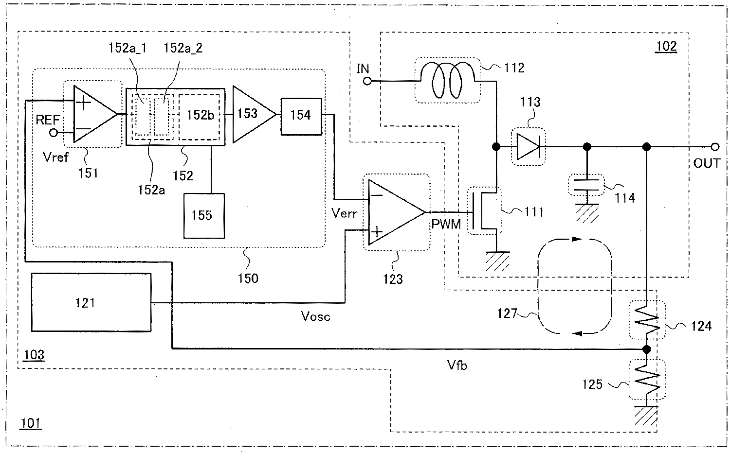
도 1은 전원 회로(101)의 일례를 도시한다. 전원 회로(101)는 전압 변환 회로(102), 및 전압 변환 회로(102)를 제어하는 제어 회로(103)를 포함하고 있다. 전압 변환 회로(102)는 트랜지스터(111), 코일(112), 다이오드(113) 및 용량 소자(114)를 포함하는 DC-DC 컨버터이다. 제어 회로(103)는 삼각파 발생 회로(121), 디지털 제어 회로(150), 펄스 폭 변조 출력 드라이버(123), 저항(124) 및 저항(125)을 포함하고 있다. 또한, 점선의 화살표(127)는 귀환 회로의 루프(loop)를 나타내고 있다. 저항(124)의 출력 전압인 귀환 전압 Vfb는 디지털 제어 회로(150)에 입력된다.1 shows an example of the
DC-DC 컨버터는 직류 전압을 다른 직류 전압으로 변환하는 회로이다. DC-DC 컨버터의 전형적인 변환 방식은 리니어 방식이나 스위칭 방식을 포함한다. 스위칭 방식의 DC-DC 컨버터는 변환 효율이 우수하다. 본 실시 형태에서는, 스위칭 방식의 DC-DC 컨버터, 특히 트랜지스터, 코일, 다이오드 및 용량 소자를 포함하는 쵸퍼형(chopper-type) DC-DC 컨버터가 전압 변환 회로(102)로서 이용된다.A DC-DC converter is a circuit that converts a DC voltage into another DC voltage. Typical conversion schemes for DC-DC converters include linear or switching schemes. Switched DC-DC converters have excellent conversion efficiency. In this embodiment, a switching-type DC-DC converter, especially a chopper-type DC-DC converter including a transistor, a coil, a diode, and a capacitor, is used as the
디지털 제어 회로(150)는, 비교기(151), 디지털 연산 처리 회로(152), 펄스 폭 변조 출력 드라이버(153) 및 로우 패스 필터(LPF; 154)를 포함하고 있다.The
오차 증폭 회로를 디지털 제어 회로(150)로 대체하면, 회로(150) 내의 소자의 특성에 변동이 있어도 문제가 되지 않는다. 디지털 제어 회로(150)에서, 디지털 연산 처리 회로(152) 및 펄스 폭 변조 출력 드라이버(153)는 디지털 회로이다. 디지털 회로는, 회로 내의 신호의 레벨이 기준보다 높은지 또는 낮은지에 따라 신호가 1인지 0(제로)인지를 판단하고, 따라서 디지털 회로 내의 소자의 특성이 변동될 때에도 데이터를 적절히 처리한다.If the error amplifier circuit is replaced with the
또한, 디지털 제어 회로(150)에서는, 점유 면적이 큰 수동 소자(예를 들어, 용량 소자나 저항)의 사용을 억제하고 있으므로, 회로의 점유 면적을 작게 할 수 있다는 점에서 바람직하다.Moreover, since the use of the passive element (for example, capacitor | capacitance element or resistance) with large occupied area is suppressed in the
비교기(151)는 반전 입력 단자 REF로부터 입력되는 기준 전압 Vref와 귀환 전압 Vfb를 비교하여, H(하이 레벨) 또는 L(로우 레벨)의 디지털 신호, 즉 1 또는 0(제로)의 디지털 신호를 출력한다.The
디지털 연산 처리 회로(152)는 디지털 평균화 적분기(152a) 및 디지털 펄스 폭 변조기(152b)를 포함하고 있다. 디지털 평균화 적분기(152a)는 디지털 평균화 회로(152a_1) 및 디지털 적분기(152a_2)를 포함하고 있다. 디지털 연산 처리 회로(152)에는, 외부 클럭 분할기(155)가 접속되고, 클럭 분할기(155)로부터의 클럭 신호가 입력된다.The digital
디지털 연산 처리 회로(152)는 비교기(151)로부터 출력된 디지털 신호를 평균화 처리, 적분화 처리 및 디지털 펄스 폭 변조 처리를 행한다. 디지털 평균화 적분기(152a)에서, 디지털 평균화 회로(152a_1)가 평균화 처리를 행하고, 디지털 적분기(152a_2)가 적분화 처리를 행한다. 디지털 펄스 폭 변조기(152b)가 디지털 펄스 폭 변조 처리를 행한다.The digital
디지털 연산 처리 회로(152)는, 비교기(151)로부터 출력된 디지털 신호(H(하이 레벨) 또는 L(로우 레벨))에 대해 N 비트의 데이터를 유지하고, H 신호와 L 신호의 출현 빈도를 비교하여, 높은 빈도의 신호를 출력한다. 따라서, 디지털 신호가 평균화된다.The digital
도 6 및 도 7은 도 1에 도시된 디지털 평균화·적분기(152a) 내에 있으며 평균화를 행하는 디지털 평균화 회로(152a_1)의 구체적인 회로 구성을 도시한다. 도 6에 도시하는 가산 회로(201)는 디지털 평균화 회로(152a_1)의 일례이다.6 and 7 show a specific circuit configuration of the digital averaging circuit 152a_1 in the digital averaging /
가산 회로(201)는 매 카운트마다 비교기(151)로부터 신호 COMP의 값을 검출하고, 신호 COMP의 값이 H(하이 레벨)이면, H(하이 레벨)을 유지한다. 예를 들어, 가산 회로(201)는 7 카운트마다 평균화된 디지털 신호 DIG_AVE를 출력한다. 본 실시 형태에서는, H(하이 레벨)의 신호 COMP가 4회 이상 입력되면, H(하이 레벨)의 디지털 신호 DIG_AVE를 출력하고, H(하이 레벨)의 신호 COMP가 3회 이하로 입력되면, L(로우 레벨)의 디지털 신호 DIG_AVE를 출력한다. 또한, 저장된 신호 COMP는 리세트 신호 RST에 의해 8 카운트마다 리세트된다.The
가산 회로(201)는 가산기(251), 가산기(252) 및 가산기(253)를 포함한다.The
가산기(251)의 제1 단자에는, 가산기(252)의 제1 단자 및 가산기(253)의 제1 단자가 접속되어 있고, 제어 리세트 신호 CNT_RST가 입력된다. 제어 리세트 신호 CNT_RST는 가산 회로(201)의 데이터를 리세트하는 신호이다. 가산기(251)의 제2 단자에는, 비교기(151)로부터 신호 COMP가 입력된다. 가산기(251)의 제3 단자에는, 가산기(252)의 제3 단자 및 가산기(253)의 제3 단자가 접속되어 있고, 클럭 신호 CLK가 입력된다. 가산기(251)의 제4 단자에는, 가산기(252)의 제4 단자 및 가산기(253)의 제4 단자가 접속되어 있고, 리세트 신호 RST가 입력된다. 리세트 신호 RST는 후술의 플립플롭(214) 내의 데이터를 리세트하는 신호이다. 가산기(251)의 제5 단자에는, 가산기(252)의 제2 단자가 접속되어 있다. 가산기(251)의 제5 단자는 출력 신호 COUT를 출력한다.The first terminal of the
가산기(252)의 제1 단자에는, 가산기(251)의 제1 단자 및 가산기(253)의 제1 단자가 접속되어 있고, 제어 리세트 신호 CNT_RST가 입력된다. 가산기(252)의 제2 단자에는, 가산기(251)의 제5 단자가 접속되어 있다. 가산기(251)의 제5 단자로부터 출력된 출력 신호 COUT는 입력 신호 CIN으로서 가산기(252)의 제2 단자에 입력된다. 가산기(252)의 제3 단자에는, 가산기(251)의 제3 단자 및 가산기(253)의 제3 단자가 접속되어 있고, 클럭 신호 CLK가 입력된다. 가산기(252)의 제4 단자에는, 가산기(251)의 제4 단자 및 가산기(253)의 제4 단자가 접속되어 있고, 리세트 신호 RST가 입력된다. 가산기(252)의 제5 단자에는, 가산기(253)의 제2 단자가 접속되어 있다. 가산기(252)의 제5 단자는 출력 신호 COUT를 출력한다.The first terminal of the
가산기(253)의 제1 단자에는, 가산기(251)의 제1 단자 및 가산기(252)의 제1 단자가 접속되어 있고, 제어 리세트 신호 CNT_RST가 입력된다. 가산기(253)의 제2 단자에는, 가산기(252)의 제5 단자가 접속되어 있다. 가산기(252)의 제5 단자로부터 출력된 출력 신호 COUT는 입력 신호 CIN으로서 가산기(253)의 제2 단자에 입력된다. 가산기(253)의 제3 단자에는, 가산기(251)의 제3 단자 및 가산기(252)의 제3 단자가 접속되어 있고, 클럭 신호 CLK가 입력된다. 가산기(253)의 제4 단자에는, 가산기(251)의 제4 단자 및 가산기(252)의 제4 단자가 접속되어 있고, 리세트 신호 RST가 입력된다. 가산기(253)의 제5 단자는 평균화된 디지털 신호 DIG_AVE를 출력한다.The first terminal of the
도 7은 가산기(251) 내지 가산기(253) 각각의 회로도를 도시한다. 가산기(251) 내지 가산기(253)의 각각은 AND 게이트(211), AND 게이트(212), XOR 게이트(213) 및 플립플롭(flip-flop; FF))(214)을 포함하고 있다.7 shows a circuit diagram of each of
AND 게이트(211)의 제1 입력 단자에는, XOR 게이트(213)의 제1 입력 단자가 접속되고, 입력 신호 CIN이 입력된다. AND 게이트(211)의 제2 입력 단자에는, XOR 게이트(213)의 제2 입력 단자 및 플립플롭(214)의 제4 단자가 접속된다. AND 게이트(211)의 출력 단자는 출력 신호 COUT를 출력한다.The first input terminal of the
AND 게이트(212)의 제1 입력 단자에는, 제어 리세트 신호 CNT_RST가 입력된다. AND 게이트(212)의 제2 입력 단자에는, XOR 게이트(213)의 출력 단자가 접속된다. AND 게이트(212)의 출력 단자에는, 플립플롭(214)의 제1 단자가 접속된다.The control reset signal CNT_RST is input to the first input terminal of the AND
XOR 게이트(213)의 제1 입력 단자에는, AND 게이트(211)의 제1 입력 단자가 접속되어 있고, 입력 신호 CIN이 입력된다. XOR 게이트(213)의 제2 입력 단자에는, AND 게이트(211)의 제2 입력 단자 및 플립플롭(214)의 제4 단자가 접속되어 있다. XOR 게이트(213)의 출력 단자에는, AND 게이트(212)의 제2 입력 단자가 접속되어 있다.The first input terminal of the AND
플립플롭(214)의 제1 단자에는, AND 게이트(212)의 출력 단자가 접속되어 있다. 플립플롭(214)의 제2 단자에는, 리세트 신호 RST가 입력된다. 플립플롭(214)의 제3 단자에는, 클럭 신호 CLK가 입력된다. 플립플롭(214)의 제4 단자에는, AND 게이트(211)의 제2 입력 단자 및 XOR 게이트(213)의 제2 입력 단자가 접속되어 있다.The output terminal of the AND
그 다음, 디지털 적분기(152a_2)는, 평균화된 디지털 신호 DIG_AVE에 따라 "-1" 또는 "+1"을 가산하고, 적분을 행한다. 평균화된 디지털 신호 DIG_AVE가 H(하이 레벨)이면, "-1"이 가산되고, 평균화된 디지털 신호 DIG_AVE가 L(로우 레벨)이면, "+1"이 가산된다는 점에 유의한다. 따라서, 평균화된 디지털 신호 DIG_AVE가 적분된다.Then, the digital integrator 152a_2 adds " -1 " or " + 1 " in accordance with the averaged digital signal DIG_AVE and performs integration. Note that "-1" is added if the averaged digital signal DIG_AVE is H (high level), and "+1" is added if the averaged digital signal DIG_AVE is L (low level). Thus, the averaged digital signal DIG_AVE is integrated.
도 8은 도 1에서의 디지털 평균화·적분기(152a) 내의 특정 회로이며 적분을 행하는 디지털 적분기(152a_2)(가감산 회로(202))의 회로 구성을 도시한다. 도 8은 또한 도 1의 디지털 펄스 폭 변조기(152b)의 회로 구성(카운트 비교 회로(203) 및 래치 회로(204))를 도시한다.FIG. 8 shows a circuit configuration of the digital integrator 152a_2 (addition / subtraction circuit 202) which is a specific circuit in the digital averaging /
가감산 회로(202)의 제1 단자에는, 래치 회로(204)의 제1 단자가 접속되어 있고, 리세트 신호 RST가 입력된다. 가감산 회로(202)의 제2 단자에는, 클럭 신호 CLK가 입력된다. 가감산 회로(202)의 제3 단자에는, 평균화된 디지털 신호 DIG_AVE가 입력된다. 가감산 회로(202)의 제4 단자에는, 카운트 비교 회로(203)의 제1 단자가 접속되어 있다. 가감산 회로(202)의 제4 단자는 신호 SET-CNT0을 출력한다. 가감산 회로(202)의 제5 단자에는, 카운트 비교 회로(203)의 제2 단자가 접속되어 있다. 가감산 회로(202)의 제5 단자는 신호 SET-CNT1을 출력한다. 가감산 회로(202)의 제6 단자에는, 카운트 비교 회로(203)의 제3 단자가 접속되어 있다. 가감산 회로(202)의 제6 단자는 신호 SET-CNT2를 출력한다. 가감산 회로(202)의 제7 단자에는, 카운트 비교 회로(203)의 제4 단자가 접속되어 있다. 가감산 회로(202)의 제7 단자는 신호 SET-CNT3을 출력한다. 가감산 회로(202)의 제8 단자에는, 카운트 비교 회로(203)의 제5 단자가 접속되어 있다. 가감산 회로(202)의 제8 단자는 신호 SET-CNT4를 출력한다. 가감산 회로(202)의 제9 단자에는, 카운트 비교 회로(203)의 제6 단자가 접속되어 있다. 가감산 회로(202)의 제9 단자는 신호 SET-CNT5를 출력한다. 가감산 회로(202)의 제10 단자에는, 카운트 비교 회로(203)의 제7 단자가 접속되어 있다. 가감산 회로(202)의 제10 단자는 리미트 신호 LIMIT를 출력한다.The first terminal of the
신호 SET-CNT0 내지 신호 SET-CNT5에는, 클럭 신호 CLK가 입력될 때마다, "-1" 또는 "+1"이 가산된다: 입력된 평균화 디지털 신호 DIG_AVE가 H(하이 레벨) 신호인 경우에는 "-1"이 가산되고, 입력된 평균화 디지털 신호 DIG_AVE가 L(로우 레벨) 신호인 경우에는 "+1"이 가산된다. 이어서, 신호 SET-CNT0 내지 신호 SET-CNT5가 출력된다.Whenever the clock signal CLK is input, "-1" or "+1" is added to the signal SET-CNT0 to the signal SET-CNT5: when the input averaging digital signal DIG_AVE is the H (high level) signal, " -1 "is added, and" +1 "is added when the inputted averaged digital signal DIG_AVE is an L (low level) signal. Subsequently, signals SET-CNT0 to SET-CNT5 are output.
신호 SET-CNT0 내지 신호 SET-CNT5는, 후술하는 펄스 폭 W를 갖는 펄스 신호 PULSE를 생성하는 데 필요하다. 본 실시 형태에서는, 신호 SET-CNT0 내지 신호 SET-CNT5에 의해, 26-위상, 즉 64-위상 신호 PULSE가 생성될 수 있다.Signals SET-CNT0 to SET-CNT5 are necessary for generating the pulse signal PULSE having the pulse width W described later. In this embodiment, 2 6 -phase, that is, 64-phase signal PULSE can be generated by the signal SET-CNT0 to the signal SET-CNT5.
리미트 신호 LIMIT는, 후술하는 펄스 폭 W를 갖는 펄스 신호 PULSE를 생성하는 과정에서 위상을 제한하는 신호이다. 본 실시 형태에서는, 리미트 신호 LIMIT에 의해, 예를 들어 신호 SET-CNT0 내지 신호 SET-CNT5는 8 내지 56으로 제한된다. 따라서, 펄스 신호 PULSE의 펄스 폭 W의 최대값이 펄스 신호 PULSE의 주기에, 그리고 펄스 폭 W의 최소값이 0(제로)에 근접하는 것을 방지한다.The limit signal LIMIT is a signal for limiting phase in the process of generating a pulse signal PULSE having a pulse width W described later. In this embodiment, the signal SET-CNT0 to the signal SET-CNT5 are limited to 8 to 56, for example, by the limit signal LIMIT. Therefore, the maximum value of the pulse width W of the pulse signal PULSE is prevented from approaching the period of the pulse signal PULSE and the minimum value of the pulse width W approaching zero (zero).
카운트 비교 회로(203)의 제1 단자에는, 가감산 회로(202)의 제4 단자가 접속되고, 신호 SET-CNT0이 입력된다. 카운트 비교 회로(203)의 제2 단자에는, 가감산 회로(202)의 제5 단자가 접속되고, 신호 SET-CNT1이 입력된다. 카운트 비교 회로(203)의 제3 단자에는, 가감산 회로(202)의 제6 단자가 접속되고, 신호 SET-CNT2가 입력된다. 카운트 비교 회로(203)의 제4 단자에는, 가감산 회로(202)의 제7 단자가 접속되고, 신호 SET-CNT3이 입력된다. 카운트 비교 회로(203)의 제5 단자에는, 가감산 회로(202)의 제8 단자가 접속되고, 신호 SET-CNT4가 입력된다. 카운트 비교 회로(203)의 제6 단자에는, 가감산 회로(202)의 제9 단자가 접속되고, 신호 SET-CNT5가 입력된다. 카운트 비교 회로(203)의 제7 단자에는, 가감산 회로(202)의 제10 단자가 접속된다. 카운트 비교 회로(203)의 제7 단자는 리미트 신호 LIMIT를 출력한다. 카운트 비교 회로(203)의 제8 단자에는, 신호 CNT0이 입력된다. 카운트 비교 회로(203)의 제9 단자에는, 신호 CNT1이 입력된다. 카운트 비교 회로(203)의 제10 단자에는, 신호 CNT2가 입력된다. 카운트 비교 회로(203)의 제11 단자에는, 신호 CNT3이 입력된다. 카운트 비교 회로(203)의 제12 단자에는, 신호 CNT4가 입력된다. 카운트 비교 회로(203)의 제13 단자에는, 신호 CNT5가 입력된다. 카운트 비교 회로(203)의 제14 단자는 신호 HIGH-SET를 출력한다. 카운트 비교 회로(203)의 제15 단자는 신호 LOW-SET를 출력한다.The fourth terminal of the add / subtract
신호 CNT0 내지 신호 CNT5는 카운트 신호이다. 본 실시 형태에서는, 신호 CNT0 내지 신호 CNT5의 입력에 의해, 0부터 63까지 카운트할 수 있다.Signals CNT0 to CNT5 are count signals. In this embodiment, from 0 to 63 can be counted by the input of the signals CNT0 to CNT5.
신호 HIGH-SET 및 신호 LOW-SET는, 펄스 폭 변조 출력 신호 PWM이 H(하이 레벨) 또는 L(로우 레벨)인 지를 결정한다. 신호 HIGH-SET가 입력되면, 펄스 폭 변조 출력 신호 PWM은 H(하이 레벨) 신호가 된다. 신호 LOW-SET가 입력되면, 펄스 폭 변조 출력 신호 PWM은 L(로우 레벨) 신호가 된다.The signal HIGH-SET and the signal LOW-SET determine whether the pulse width modulation output signal PWM is H (high level) or L (low level). When the signal HIGH-SET is input, the pulse width modulated output signal PWM becomes an H (high level) signal. When the signal LOW-SET is input, the pulse width modulated output signal PWM becomes an L (low level) signal.
래치 회로(204)의 제1 단자에는, 가감산 회로(202)의 제1 단자가 접속되고, 리세트 신호 RST가 입력된다. 래치 회로(204)의 제2 단자에는, 카운트 비교 회로(203)의 제14 단자가 접속되고, 신호 HIGH-SET가 입력된다. 래치 회로(204)의 제3 단자에는, 카운트 비교 회로(203)의 제15 단자가 접속되고, 신호 LOW-SET가 입력된다. 래치 회로(204)의 제4 단자로부터, 펄스 폭 변조 출력 신호 PWM이 출력된다. 래치 회로(204)의 제5 단자에는, 클럭 신호 CLK가 입력된다.The first terminal of the addition /
도 9는 가감산 회로(202)의 구체적인 회로 구조를 도시한다.9 shows a specific circuit structure of the addition and
도 9에 도시된 가감산 회로(202)는 인버터(261), 인버터(262), NOR 게이트(263), 가산기(254), 가산기(255), 가산기(256), 가산기(257), 가산기(258) 및 가산기(259)를 포함하고 있다.The adder /
인버터(261)의 입력 단자에는, 평균화된 디지털 신호 DIG_AVE가 입력된다. 인버터(261)의 출력 단자는 NOR 게이트(263)의 제1 입력 단자에 접속된다.The averaged digital signal DIG_AVE is input to an input terminal of the
인버터(262)의 입력 단자에는, NOR 게이트(263)의 제2 입력 단자가 접속되고, 리미트 신호 LIMIT가 입력된다. 인버터(262)의 출력 단자에는, 가산기(254)의 제1 단자가 접속된다.The second input terminal of the NOR
NOR 게이트(263)의 제1 입력 단자에는, 인버터(261)의 출력 단자가 접속된다. NOR 게이트(263)의 제2 입력 단자에는, 인버터(262)의 입력 단자가 접속되고, 리미트 신호 LIMIT가 입력된다.An output terminal of the
가산기(254)의 제1 단자에는, 인버터(262)의 출력 단자가 접속된다. 가산기(254)의 제2 단자에는, 가산기(255)의 제2 단자, 가산기(256)의 제2 단자, 가산기(257)의 제2 단자, 가산기(258)의 제2 단자 및 가산기(259)의 제2 단자가 접속되어 있고, 클럭 신호 CLK가 입력된다. 가산기(254)의 제3 단자에는, 가산기(255)의 제3 단자, 가산기(256)의 제3 단자, 가산기(257)의 제3 단자, 가산기(258)의 제3 단자 및 가산기(259)의 제3 단자가 접속되어 있고, 리세트 신호 RST가 입력된다. 가산기(254)의 제4 단자에는, NOR 게이트(263)의 출력 단자, 가산기(255)의 제4 단자, 가산기(256)의 제4 단자, 가산기(257)의 제4 단자, 가산기(258)의 제4 단자 및 가산기(259)의 제4 단자가 접속되어 있다. 가산기(254)의 제5 단자에는, 가산기(255)의 제1 단자가 접속되어 있고, 가산기(254)의 제5 단자는 신호 SET_CNT0을 출력한다.The output terminal of the
가산기(255)의 제1 단자에는, 가산기(254)의 제5 단자가 접속되고, 신호 SET_CNT0이 입력된다. 가산기(255)의 제2 단자에는, 가산기(254)의 제2 단자, 가산기(256)의 제2 단자, 가산기(257)의 제2 단자, 가산기(258)의 제2 단자 및 가산기(259)의 제2 단자가 접속되어 있고, 클럭 신호 CLK가 입력된다. 가산기(255)의 제3 단자에는, 가산기(254)의 제3 단자, 가산기(256)의 제3 단자, 가산기(257)의 제3 단자, 가산기(258)의 제3 단자 및 가산기(259)의 제3 단자가 접속되어 있고, 리세트 신호 RST가 입력된다. 가산기(255)의 제4 단자에는, NOR 게이트(263)의 출력 단자, 가산기(254)의 제4 단자, 가산기(256)의 제4 단자, 가산기(257)의 제4 단자, 가산기(258)의 제4 단자 및 가산기(259)의 제4 단자가 접속되어 있다. 가산기(255)의 제5 단자에는, 가산기(256)의 제1 단자가 접속되어 있고, 가산기(255)의 제5 단자는 신호 SET_CNT1을 출력한다.The fifth terminal of the
가산기(256)의 제1 단자에는, 가산기(255)의 제5 단자가 접속되고, 신호 SET_CNT1이 입력된다. 가산기(256)의 제2 단자에는, 가산기(254)의 제2 단자, 가산기(255)의 제2 단자, 가산기(257)의 제2 단자, 가산기(258)의 제2 단자 및 가산기(259)의 제2 단자가 접속되어 있고, 클럭 신호 CLK가 입력된다. 가산기(256)의 제3 단자에는, 가산기(254)의 제3 단자, 가산기(255)의 제3 단자, 가산기(257)의 제3 단자, 가산기(258)의 제3 단자 및 가산기(259)의 제3 단자가 접속되어 있고, 리세트 신호 RST가 입력된다. 가산기(256)의 제4 단자에는, NOR 게이트(263)의 출력 단자, 가산기(254)의 제4 단자, 가산기(255)의 제4 단자, 가산기(257)의 제4 단자, 가산기(258)의 제4 단자 및 가산기(259)의 제4 단자가 접속되어 있다. 가산기(256)의 제5 단자에는, 가산기(257)의 제1 단자가 접속되어 있고, 가산기(256)의 제5 단자는 신호 SET_CNT2를 출력한다.The fifth terminal of the
가산기(257)의 제1 단자에는, 가산기(256)의 제5 단자가 접속되고, 신호 SET_CNT2가 입력된다. 가산기(257)의 제2 단자에는, 가산기(254)의 제2 단자, 가산기(255)의 제2 단자, 가산기(256)의 제2 단자, 가산기(258)의 제2 단자 및 가산기(259)의 제2 단자가 접속되어 있고, 클럭 신호 CLK가 입력된다. 가산기(257)의 제3 단자에는, 가산기(254)의 제3 단자, 가산기(255)의 제3 단자, 가산기(256)의 제3 단자, 가산기(258)의 제3 단자 및 가산기(259)의 제3 단자가 접속되어 있고, 리세트 신호 RST가 입력된다. 가산기(257)의 제4 단자에는, NOR 게이트(263)의 출력 단자, 가산기(254)의 제4 단자, 가산기(255)의 제4 단자, 가산기(256)의 제4 단자, 가산기(258)의 제4 단자 및 가산기(259)의 제4 단자가 접속되어 있다. 가산기(257)의 제5 단자에는, 가산기(258)의 제1 단자가 접속되어 있고, 가산기(257)의 제5 단자는 신호 SET_CNT3을 출력한다.The fifth terminal of the
가산기(258)의 제1 단자에는, 가산기(257)의 제5 단자가 접속되고, 신호 SET_CNT3이 입력된다. 가산기(258)의 제2 단자에는, 가산기(254)의 제2 단자, 가산기(255)의 제2 단자, 가산기(256)의 제2 단자, 가산기(257)의 제2 단자 및 가산기(259)의 제2 단자가 접속되어 있고, 클럭 신호 CLK가 입력된다. 가산기(258)의 제3 단자에는, 가산기(254)의 제3 단자, 가산기(255)의 제3 단자, 가산기(256)의 제3 단자, 가산기(257)의 제3 단자 및 가산기(259)의 제3 단자가 접속되어 있고, 리세트 신호 RST가 입력된다. 가산기(258)의 제4 단자에는, NOR 게이트(263)의 출력 단자, 가산기(254)의 제4 단자, 가산기(255)의 제4 단자, 가산기(256)의 제4 단자, 가산기(257)의 제4 단자 및 가산기(259)의 제4 단자가 접속되어 있다. 가산기(258)의 제5 단자에는, 가산기(259)의 제1 단자가 접속되어 있고, 가산기(258)의 제5 단자는 신호 SET_CNT4를 출력한다.The fifth terminal of the
가산기(259)의 제1 단자에는, 가산기(258)의 제5 단자가 접속되고, 신호 SET_CNT4가 입력된다. 가산기(259)의 제2 단자에는, 가산기(254)의 제2 단자, 가산기(255)의 제2 단자, 가산기(256)의 제2 단자, 가산기(257)의 제2 단자 및 가산기(258)의 제2 단자가 접속되어 있고, 클럭 신호 CLK가 입력된다. 가산기(259)의 제3 단자에는, 가산기(254)의 제3 단자, 가산기(255)의 제3 단자, 가산기(256)의 제3 단자, 가산기(257)의 제3 단자 및 가산기(258)의 제3 단자가 접속되어 있고, 리세트 신호 RST가 입력된다. 가산기(259)의 제4 단자에는, NOR 게이트(263)의 출력 단자, 가산기(254)의 제4 단자, 가산기(255)의 제4 단자, 가산기(256)의 제4 단자, 가산기(257)의 제4 단자 및 가산기(258)의 제4 단자가 접속되어 있다. 가산기(259)의 제5 단자는 신호 SET_CNT5를 출력한다.The fifth terminal of the
도 10은 가산기(254) 내지 가산기(259) 각각의 회로도를 도시한다. 가산기(254) 내지 가산기(259)의 각각은 AND 게이트(221), AND 게이트(222), OR 게이트(224), XOR 게이트(225), XOR 게이트(226) 및 플립플롭(227)을 포함한다.10 shows a circuit diagram of each of
AND 게이트(221)의 제1 입력 단자에는, XOR 게이트(225)의 제1 입력 단자가 접속되어 있고, 제어 신호 CONT가 입력된다. 제어 신호 CONT는, 후속 단계에서 가산 또는 감산 중 어느 하나를 수행할 것을 가산기에 나타내는 신호이다. AND 게이트(221)의 제2 입력 단자에는, XOR 게이트(225)의 제2 입력 단자 및 플립플롭(227)의 제4 단자가 접속되어 있다. AND 게이트(221)의 출력 단자에는, OR 게이트(224)의 제1 입력 단자가 접속되어 있다.The first input terminal of the
AND 게이트(222)의 제1 입력 단자에는, XOR 게이트(226)의 제1 입력 단자가 접속되어 있고, 입력 신호 CIN이 입력된다. AND 게이트(222)의 제2 입력 단자에는, XOR 게이트(225)의 출력 단자 및 XOR 게이트(226)의 제2 입력 단자가 접속되어 있다. AND 게이트(222)의 출력 단자에는, OR 게이트(224)의 제2 입력 단자가 접속되어 있다.The first input terminal of the
OR 게이트(224)의 제1 입력 단자에는, AND 게이트(221)의 출력 단자가 접속되어 있다. OR 게이트(224)의 제2 입력 단자에는, AND 게이트(222)의 출력 단자가 접속되어 있다. OR 게이트(224)의 출력 단자는 출력 신호 COUT를 출력한다.The output terminal of the AND
XOR 게이트(225)의 제1 입력 단자에는, AND 게이트(221)의 제1 입력 단자가 접속되어 있고, 제어 신호 CONT가 입력된다. XOR 게이트(225)의 제2 입력 단자에는, AND 게이트(221)의 제2 입력 단자 및 플립플롭(227)의 제4 단자가 접속되어 있다. XOR 게이트(225)의 출력 단자에는, AND 게이트(222)의 제2 입력 단자 및 XOR 게이트(226)의 제2 입력 단자가 접속되어 있다.The first input terminal of the AND
XOR 게이트(226)의 제1 입력 단자에는, AND 게이트(222)의 제1 입력 단자가 접속되어 있고, 입력 신호 CIN이 입력된다. XOR 게이트(226)의 제2 입력 단자에는, AND 게이트(222)의 제2 입력 단자 및 XOR 게이트(225)의 출력 단자가 접속되어 있다. XOR 게이트(226)의 출력 단자에는, 플립플롭(227)의 제1 단자에 접속되어 있다.The first input terminal of the AND
플립플롭(227)의 제1 단자에는, XOR 게이트(226)의 출력 단자가 접속되어 있다. 플립플롭(227)의 제2 단자에는, 리세트 신호 RST가 입력된다. 플립플롭(227)의 제3 단자에는, 클럭 신호 CLK가 입력된다. 플립플롭(227)의 제4 단자에는, AND 게이트(221)의 제2 입력 단자 및 XOR 게이트(225)의 제2 입력 단자가 접속되어 있다.An output terminal of the
디지털 펄스 폭 변조기(152b)는 적분된 디지털 신호에 따라 펄스 폭 변조의 펄스 폭을 설정한다. 따라서, 디지털 펄스 폭 변조 처리가 행해진다. 디지털 펄스 폭 변조된 펄스 폭 변조 출력 신호 PWM은 펄스 폭 변조 출력 드라이버(153)에 입력된다.The digital
도 11 및 도 12는 디지털 펄스 폭 변조기(152b)의 구체적인 회로 구성을 도시한다. 도 11에 도시된 카운트 비교 회로(203) 및 도 12에 도시된 래치 회로(204)는 디지털 펄스 폭 변조기(152b)의 구체 예이다. 카운트 비교 회로(203)는 신호 SET_CNT0 내지 신호 SET_CNT5에 의해 결정된 듀티비의 미리 정해진 값과 신호 CNT0 내지 신호 CNT5의 값을 비교하여, 이들이 일치하면 펄스 폭 변조 출력 신호 PWM을 생성한다.11 and 12 show a specific circuit configuration of the digital
도 11은 카운트 비교 회로(203)의 회로도를 도시한다.11 shows a circuit diagram of the
카운트 비교 회로(203)는 XOR 게이트(271), XOR 게이트(272), XOR 게이트(273), XOR 게이트(274), XOR 게이트(275), XOR 게이트(276), NAND 게이트(277), AND 게이트(278), OR 게이트(279), NAND 게이트(281) 및 NAND 게이트(282)를 포함하고 있다.The
XOR 게이트(271)의 제1 입력 단자에는, NAND 게이트(281)의 제1 입력 단자가 접속되어 있고, 신호 CNT0이 입력된다. XOR 게이트(271)의 제2 입력 단자에는, 신호 SET_CNT0이 입력된다. XOR 게이트(271)의 출력 단자에는, NAND 게이트(282)의 제1 입력 단자가 접속되어 있다.The first input terminal of the
XOR 게이트(272)의 제1 입력 단자에는, NAND 게이트(281)의 제2 입력 단자가 접속되어 있고, 신호 CNT1이 입력된다. XOR 게이트(272)의 제2 입력 단자에는, 신호 SET_CNT1이 입력된다. XOR 게이트(272)의 출력 단자에는, NAND 게이트(282)의 제2 입력 단자가 접속되어 있다.The second input terminal of the
XOR 게이트(273)의 제1 입력 단자에는, NAND 게이트(281)의 제3 입력 단자가 접속되어 있고, 신호 CNT2가 입력된다. XOR 게이트(273)의 제2 입력 단자에는, 신호 SET_CNT2가 입력된다. XOR 게이트(273)의 출력 단자에는, NAND 게이트(282)의 제3 입력 단자가 접속되어 있다.The third input terminal of the
XOR 게이트(274)의 제1 입력 단자에는, NAND 게이트(281)의 제4 입력 단자가 접속되어 있고, 신호 CNT3이 입력된다. XOR 게이트(274)의 제2 입력 단자에는, NAND 게이트(277)의 제1 입력 단자 및 AND 게이트(278)의 제1 입력 단자가 접속되어 있고, 신호 SET_CNT3이 입력된다. XOR 게이트(274)의 출력 단자에는, NAND 게이트(282)의 제4 입력 단자가 접속되어 있다.The fourth input terminal of the
XOR 게이트(275)의 제1 입력 단자에는, NAND 게이트(281)의 제5 입력 단자가 접속되어 있고, 신호 CNT4가 입력된다. XOR 게이트(275)의 제2 입력 단자에는, NAND 게이트(277)의 제2 입력 단자 및 AND 게이트(278)의 제2 입력 단자가 접속되어 있고, 신호 SET_CNT4가 입력된다. XOR 게이트(275)의 출력 단자에는, NAND 게이트(282)의 제5 입력 단자가 접속되어 있다.The fifth input terminal of the
XOR 게이트(276)의 제1 입력 단자에는, NAND 게이트(281)의 제6 입력 단자가 접속되어 있고, 신호 CNT5가 입력된다. XOR 게이트(276)의 제2 입력 단자에는, NAND 게이트(277)의 제3 입력 단자 및 AND 게이트(278)의 제3 입력 단자가 접속되어 있고, 신호 SET_CNT5가 입력된다. XOR 게이트(276)의 출력 단자에는, NAND 게이트(282)의 제6 입력 단자가 접속되어 있다.The sixth input terminal of the
NAND 게이트(277)의 제1 입력 단자에는, XOR 게이트(274)의 제2 입력 단자 및 AND 게이트(278)의 제1 입력 단자가 접속되어 있고, 신호 SET_CNT3이 입력된다. NAND 게이트(277)의 제2 입력 단자에는, XOR 게이트(275)의 제2 입력 단자 및 AND 게이트(278)의 제2 입력 단자가 접속되어 있고, 신호 SET_CNT4가 입력된다. NAND 게이트(277)의 제3 입력 단자에는, XOR 게이트(276)의 제2 입력 단자 및 AND 게이트(278)의 제3 입력 단자가 접속되어 있고, 신호 SET_CNT5가 입력된다. NAND 게이트(277)의 출력 단자에는, OR 게이트(279)의 제1 입력 단자가 접속되어 있다.The second input terminal of the
AND 게이트(278)의 제1 입력 단자에는, XOR 게이트(274)의 제2 입력 단자 및 NAND 게이트(277)의 제1 입력 단자가 접속되어 있고, 신호 SET_CNT3이 입력된다. AND 게이트(278)의 제2 입력 단자에는, XOR 게이트(275)의 제2 입력 단자 및 NAND 게이트(277)의 제2 입력 단자가 접속되어 있고, 신호 SET_CNT4가 입력된다. AND 게이트(278)의 제3 입력 단자에는, XOR 게이트(276)의 제2 입력 단자 및 NAND 게이트(277)의 제3 입력 단자가 접속되어 있고, 신호 SET_CNT5가 입력된다. AND 게이트(278)의 출력 단자에는, OR 게이트(279)의 제2 입력 단자가 접속되어 있다.The second input terminal of the
OR 게이트(279)의 제1 입력 단자에는, NAND 게이트(277)의 출력 단자가 접속되어 있다. OR 게이트(279)의 제2 입력 단자에는, AND 게이트(278)의 출력 단자가 접속되어 있다. OR 게이트(279)의 출력 단자는 리미트 신호 LIMIT를 출력한다.An output terminal of the
NAND 게이트(281)의 제1 입력 단자에는, XOR 게이트(271)의 제1 입력 단자가 접속되어 있고, 신호 CNT0이 입력된다. NAND 게이트(281)의 제2 입력 단자에는, XOR 게이트(272)의 제1 입력 단자가 접속되어 있고, 신호 CNT1이 입력된다. NAND 게이트(281)의 제3 입력 단자에는, XOR 게이트(273)의 제1 입력 단자가 접속되어 있고, 신호 CNT2가 입력된다. NAND 게이트(281)의 제4 입력 단자에는, XOR 게이트(274)의 제1 입력 단자가 접속되어 있고, 신호 CNT3이 입력된다. NAND 게이트(281)의 제5 입력 단자에는, XOR 게이트(275)의 제1 입력 단자가 접속되어 있고, 신호 CNT4가 입력된다. NAND 게이트(281)의 제6 입력 단자에는, XOR 게이트(276)의 제1 입력 단자가 접속되어 있고, 신호 CNT5가 입력된다. NAND 게이트(281)의 출력 단자는 신호 LOW-SET를 출력한다.The first input terminal of the
NAND 게이트(282)의 제1 입력 단자에는, XOR 게이트(271)의 출력 단자가 접속된다. NAND 게이트(282)의 제2 입력 단자에는, XOR 게이트(272)의 출력 단자가 접속된다. NAND 게이트(282)의 제3 입력 단자에는, XOR 게이트(273)의 출력 단자가 접속된다. NAND 게이트(282)의 제4 입력 단자에는, XOR 게이트(274)의 출력 단자가 접속된다. NAND 게이트(282)의 제5 입력 단자에는, XOR 게이트(275)의 출력 단자가 접속된다. NAND 게이트(282)의 제6 입력 단자에는, XOR 게이트(276)의 출력 단자가 접속된다. NAND 게이트(282)의 출력 단자는 신호 HIGH-SET를 출력한다.An output terminal of the
도 12는 래치 회로(204)의 회로도를 도시한다. 래치 회로(204)는 플립플롭(241), 플립플롭(242), NOR 게이트(243) 및 NOR 게이트(244)를 포함한다.12 shows a circuit diagram of the
플립플롭(241)의 제1 단자에는, 신호 LOW-SET가 입력된다. 플립플롭(241)의 제2 단자에는, 플립플롭(242)의 제2 단자, NOR 게이트(243)의 제2 입력 단자 및 NOR 게이트(244)의 제2 입력 단자가 접속되어 있고, 리세트 신호 RST가 입력된다. 플립플롭(241)의 제3 단자에는, 플립플롭(242)의 제3 단자가 접속되어 있고, 클럭 신호 CLK가 입력된다. 플립플롭(241)의 제4 단자에는, NOR 게이트(243)의 제1 입력 단자가 접속되어 있다.The signal LOW-SET is input to the first terminal of the flip-
플립플롭(242)의 제1 단자에는, 신호 HIGH-SET가 입력된다. 플립플롭(242)의 제2 단자에는, 플립플롭(241)의 제2 단자, NOR 게이트(243)의 제2 입력 단자 및NOR 게이트(244)의 제2 입력 단자가 접속되어 있고, 리세트 신호 RST가 입력된다. 플립플롭(242)의 제3 단자에는, 플립플롭(241)의 제3 단자가 접속되어 있고, 클럭 신호 CLK가 입력된다. 플립플롭(242)의 제4 단자에는, NOR 게이트(244)의 제1 입력 단자가 접속되어 있다.The signal HIGH-SET is input to the first terminal of the flip-
NOR 게이트(243)의 제1 입력 단자에는, 플립플롭(241)의 제4 단자가 접속되어 있다. NOR 게이트(243)의 제2 입력 단자에는, 플립플롭(241)의 제2 단자, 플립플롭(242)의 제2 단자 및 NOR 게이트(244)의 제2 입력 단자가 접속되어 있고, 리세트 신호 RST가 입력된다. NOR 게이트(243)의 제3 입력 단자에는, NOR 게이트(244)의 출력 단자가 접속되어 있다. NOR 게이트(243)의 출력 단자에는, NOR 게이트(244)의 제3 입력 단자가 접속되어 있다.The fourth terminal of the flip-
NOR 게이트(244)의 제1 입력 단자에는, 플립플롭(242)의 제4 단자가 접속되어 있다. NOR 게이트(244)의 제2 입력 단자에는, 플립플롭(241)의 제2 단자, 플립플롭(242)의 제2 단자 및 NOR 게이트(243)의 제2 입력 단자가 접속되어 있고, 리세트 신호 RST가 입력된다. NOR 게이트(244)의 제3 입력 단자에는, NOR 게이트(243)의 출력 단자가 접속되어 있다. NOR 게이트(244)의 출력 단자에는, NOR 게이트(243)의 제3 입력 단자가 접속되어 있다. NOR 게이트(244)의 출력 단자는 펄스 폭 변조 출력 신호 PWM을 출력한다.The fourth terminal of the flip-
이제, 도 2의 (a) 내지 (c)를 참조하여 디지털 펄스 폭 변조에 대해서 설명한다.Now, digital pulse width modulation will be described with reference to FIGS. 2A to 2C.
디지털 펄스 신호 PULSE의 펄스 폭은 W, 그 펄스 주기는 T로 칭한다(도 2의 (a) 참조). 펄스 신호 PULSE는 클럭 분할기(155)로부터의 클럭 및 신호 SET_CNT0 내지 SET_CNT5에 의해 제어되는 위상에 기초하여 생성된다. 펄스 신호 PULSE는 펄스 폭 변조 출력 신호 PWM에 상당한다. 듀티비 Di는, 이하의 식 1에 의해 나타낸다.The pulse width of the digital pulse signal PULSE is referred to as W and its pulse period is referred to as T (see Fig. 2A). The pulse signal PULSE is generated based on the clock from the
![]()
![]()
도 2의 (a)는 식(1)에서, n=6 및 i=32인 경우의 펄스 신호 PULSE를 나타내고, 도 2의 (b)는 식(1)에서, n=6 및 i=48인 경우의 펄스 신호 PULSE를 나타내며, 도 2의 (c)는 식(1)에서, n=6 및 i=16인 경우의 펄스 신호 PULSE를 나타낸다.(A) of FIG. 2 shows the pulse signal PULSE when n = 6 and i = 32 in Formula (1), and FIG. 2 (b) shows n = 6 and i = 48 in Formula (1). The pulse signal PULSE in this case is shown, and (c) of FIG. 2 shows the pulse signal PULSE in the case of n = 6 and i = 16 in Formula (1).
i=32이면, 듀티비 D32는 0.5이고, i=48이면, 듀티비 D48은 0.75이며, i=16이면, 듀티비 D16은 0.25이다. 후술하는 전원 전압 Vdd는 듀티비에 따라 생성된다. 디지털 신호가 아날로그 신호로 변환됨으로써, DA 컨버터에 의한 처리와 유사한 처리가 수행된다.If i = 32, the duty ratio D32 is 0.5; if i = 48, the duty ratio D48 is 0.75; if i = 16, the duty ratio D16 is 0.25. The power supply voltage Vdd described later is generated according to the duty ratio. By converting the digital signal into an analog signal, processing similar to that by the DA converter is performed.
예로서, 1 MHz의 클럭을 이용하여 펄스 폭 변조되는 15.525 kHz의 펄스 폭 변조 출력 신호를 출력하는 방법에 대해서 설명한다.As an example, a method of outputting a pulse width modulated output signal of 15.525 kHz that is pulse width modulated using a clock of 1 MHz will be described.
1 MHz(1 ㎲) 클럭을 이용하여, 15.525 kHz(64 ㎲)의 펄스 폭 변조 출력 신호를 생성하면, 64-위상의 펄스 폭 변조 출력 신호가 출력될 수 있다.Using a 1 MHz (1 kHz) clock to generate a pulse width modulated output signal of 15.525 kHz (64 kHz), a 64-phase pulse width modulated output signal can be output.
디지털 펄스 폭 변조 처리된 펄스 폭 변조 출력 신호는 펄스 폭 변조 출력 드라이버(153)에 입력된다. 펄스 폭 변조 출력 신호는 펄스 폭 변조 출력 드라이버(153)에 의해 신호 강도를 높일 수 있다. 즉, 펄스 폭 변조 출력 신호는 펄스 폭 변조 출력 드라이버(153)에 의해 증폭된다.The pulse width modulated output signal subjected to the digital pulse width modulation process is input to the pulse width modulated
신호 강도를 높인 펄스 폭 변조 출력 신호는 평활화 회로인 로우 패스 필터(154)에 입력된다.The pulse width modulated output signal with the increased signal strength is input to the
로우 패스 필터(154)는 펄스 폭 변조 출력 신호의 고주파 성분을 차단하고, 펄스 폭 변조 출력 신호는 평활화된다. 로우 패스 필터(154)에 입력된 펄스 폭 변조 출력 신호를 이용하여, 듀티비에 상당하는 전압이 출력된다. 출력 전압 Verr는, 출력 전압 Verr =(듀티비)×(펄스 폭 변조 출력 드라이버(153)의 전원 전압)으로 나타낸다.The
즉, 디지털 신호가 아날로그 신호가 되고; 따라서 DA 컨버터에 의한 공정과 유사한 공정이 행해진다. 또한, 로우 패스 필터(154)에 의해, 주파수 응답이 행해진다.That is, the digital signal becomes an analog signal; Therefore, a process similar to that by the DA converter is performed. In addition, the
본 실시 형태에서는, 디지털 제어 회로(150)를 이용함으로써, 전원 회로(101)의 회로 동작의 열화를 억제할 수 있다.In this embodiment, the deterioration of the circuit operation of the
또한, 전원 회로(101) 내에 디지털 제어 회로(150)를 이용함으로써, 전원 회로의 면적을 줄일 수 있다.In addition, by using the
제어 회로(103)의 다른 소자에 대해서, 이하에 설명한다.Other elements of the
삼각파 발생 회로(121)는 펄스 폭 변조 신호에 필요한 삼각파 Vosc을 발생시킨다.The triangular
펄스 폭 변조 출력 드라이버(123)의 반전 입력 단자에는 디지털 제어 회로(150)의 출력 전압 Verr가 입력되고, 비반전 입력 단자에는 삼각파 발생 회로(121)에 의해 생성된 삼각파 Vosc이 입력된다.The output voltage Verr of the
펄스 폭 변조 출력 드라이버(123)는 디지털 제어 회로(150)의 출력 전압 Verr와 삼각파 Vosc의 신호 레벨을 비교한다. 삼각파 Vosc의 신호 레벨이 디지털 제어 회로(150)의 출력 전압 Verr의 신호 레벨보다 큰 경우에는, 펄스 폭 변조 출력 드라이버(123)는 H(하이 레벨)을 펄스 폭 변조 신호로서 트랜지스터(111)에 출력한다. 삼각파 Vosc의 신호 레벨이 디지털 제어 회로(150)의 출력 전압 Verr의 신호 레벨보다 작은 경우에는, 펄스 폭 변조 출력 드라이버(123)는 L(로우 레벨)을 펄스 폭 변조 신호로서 트랜지스터(111)에 출력한다.The pulse width
아날로그 회로를 감소시킴으로써, 회로 내의 소자의 특성이 변동되어도, 회로의 동작의 열화를 억제할 수 있다.By reducing the analog circuit, deterioration of the operation of the circuit can be suppressed even if the characteristics of the elements in the circuit are changed.
또한, 회로의 동작의 열화를 억제함으로써, 상기 전원 회로를 포함하는 전기 소자, 및 이러한 전기 소자를 포함하는 전기 기기에 문제점을 야기시키는 요인을 줄이는 것이 가능하게 된다.In addition, by suppressing deterioration of the operation of the circuit, it becomes possible to reduce the factors causing problems in the electric element including the power supply circuit and the electric device including the electric element.
아날로그 회로를 감소시킴으로써, 면적이 큰 아날로그 회로의 설치를 억제할 수 있다.By reducing the analog circuit, it is possible to suppress the installation of a large analog circuit.
면적이 큰 아날로그 회로의 설치를 억제함으로써, 집적 회로 및 이 집적 회로를 포함하는 전기 기기의 면적을 줄이는 것이 가능하다. 따라서, 집적 회로 및 이 집적 회로를 포함하는 전기 기기의 비용을 줄일 수 있다.By suppressing the installation of a large-area analog circuit, it is possible to reduce the area of the integrated circuit and the electric apparatus including the integrated circuit. Therefore, the cost of the integrated circuit and the electric apparatus including the integrated circuit can be reduced.
또한, 디지털 회로는 1 또는 0(제로) 중 어느 하나만을 출력하기 때문에, 디지털 회로 내의 모든 트랜지스터는 동일 도전형, 즉 n-형 트랜지스터일 수 있다. 복잡한 아날로그 신호 처리는, 동일 도전형을 갖는 아날로그 회로 트랜지스터에서는 매우 어렵다. 따라서, 본 실시 형태에서는, 디지털 회로는 동일 도전형을 갖는 트랜지스터를 이용해서 제작될 수 있다.Also, since the digital circuit only outputs either 1 or 0 (zero), all transistors in the digital circuit may be of the same conductivity type, i.e., n-type transistors. Complex analog signal processing is very difficult in analog circuit transistors having the same conductivity type. Therefore, in this embodiment, the digital circuit can be manufactured using transistors having the same conductivity type.
[실시 형태 2] Embodiment 2
본 실시 형태에서는, 제1 실시 형태에서 설명된 트랜지스터(111), 및 비교기(151), 디지털 연산 처리 회로(152) 및 펄스 폭 변조 출력 드라이버(153)의 각각에 포함되는 트랜지스터에 대해서 설명한다.In this embodiment, a transistor included in each of the
본 실시 형태는 도 3의 (a)와 (b), 및 도 4의 (a) 내지 (e)을 이용하여 설명한다.This embodiment is demonstrated using FIG.3 (a), (b), and FIG.4 (a)-(e).
도 3의 (a)와 (b)는 트랜지스터의 상면 및 단면 구조의 일례를 나타낸다. 도 3의 (a)는 톱 게이트 구조의 트랜지스터(410)의 상면도이며, 도 3의 (b)는 도 3의 (a)의 선 A-A’을 따라 절취된 단면도이다.3 (a) and 3 (b) show examples of the top and cross-sectional structures of a transistor. FIG. 3A is a top view of the
트랜지스터(410)는, 산화물 반도체막(412), 제1 전극(415a)(소스 전극 및 드레인 전극의 한쪽), 제2 전극(415b)(소스 전극 및 드레인 전극의 다른 쪽), 게이트 절연막(402) 및 게이트 전극(411)을 포함한다. 제1 전극(415a) 및 제2 전극(415b)에는 각각 제1 배선(414a) 및 제2 배선(414b)이 접하고 전기적으로 접속된다. 트랜지스터(410)에서, 소스 전극 및 드레인 전극인 제1 전극(415a) 및 제2 전극(415b)은 채널 형성 영역을 포함하는 산화물 반도체막(412)의 상면에서 접하고 있으므로, 트랜지스터(410)는 톱-콘택트형 트랜지스터라고 말할 수가 있다.The
도 3의 (a)에 도시하는 트랜지스터(410)는 싱글 게이트 구조의 트랜지스터이지만, 개시된 발명의 한 실시 형태는, 이 구성에 한정되는 것이 아님에 유의해야 한다. 트랜지스터는 게이트 전극들과 채널 형성 영역들을 포함하는 멀티 게이트 구조의 트랜지스터일 수 있다.Although the
도 3의 (a)와 (b)에 도시하는 트랜지스터는, 채널 형성 영역을 포함하는 산화물 반도체막(412) 위에 형성된 제1 전극(415a)(소스 전극 및 드레인 전극의 한쪽) 및 제2 전극(415b)(소스 전극 및 드레인 전극의 다른 쪽)을 포함하지만, 개시된 발명의 한 실시 형태는 이 구성에 한정되는 것이 아님에 유의해야 한다. 채널 형성 영역을 포함하는 산화물 반도체막(412)은 제1 전극(415a)(소스 전극 및 드레인 전극의 한쪽) 및 제2 전극(415b)(소스 전극 및 드레인 전극의 다른 쪽) 위에 형성될 수 있다.The transistors shown in FIGS. 3A and 3B include a
또한, 도 3의 (a)와 (b)에 도시하는 트랜지스터는 톱 게이트형 트랜지스터이지만, 개시된 발명의 한 실시 형태는 이 구성에 한정되는 것은 아니다. 트랜지스터(410)는 보텀 게이트형 트랜지스터일 수 있다. 또한, 트랜지스터(410)가 보텀 게이트형 트랜지스터이면, 소스 전극 및 드레인 전극 또는 채널 형성 영역을 포함하는 산화물 반도체막 중 어느 하나가 다른 쪽 위에 놓일 수 있다. 즉, 채널 형성 영역을 포함하는 산화물 반도체막 위에, 소스 전극 및 드레인 전극이 형성될 수 있고; 대안적으로 소스 전극 및 드레인 전극 위에, 채널 형성 영역을 포함하는 산화물 반도체막이 형성될 수 있다.In addition, although the transistor shown to Fig.3 (a) and (b) is a top gate type transistor, one embodiment of the disclosed invention is not limited to this structure. The
트랜지스터(410)의 산화물 반도체막(412)으로서, 고순도의 산화물 반도체막을 이용하면, 트랜지스터(410)의 특성이 향상된다. 이러한 고순도의 산화물 반도체막의 특성 및 고순도의 산화물 반도체막을 포함하는 트랜지스터의 특징에 대해서는, 이하에서 상세히 설명한다.When a high purity oxide semiconductor film is used as the
고순도의 산화물 반도체막에서, 산화물 반도체막을 포함하는 트랜지스터의 전기 특성에 악영향을 끼치는 불순물은 매우 적은 레벨까지 저감된다. 전기 특성에 악영향을 끼치는 불순물의 대표 예로서는, 수소를 들 수 있다. 수소는, 산화물 반도체막 내에서 캐리어의 공여체(도너(donor))가 될 수 있는 불순물이다. 산화물 반도체가 다량의 수소를 포함하게 되면, 산화물 반도체막은 n-형 도전성을 가질 수 있다. 따라서, 수소가 다량으로 포함된 산화물 반도체를 포함하는 트랜지스터는, 노멀리-온(normally-on) 트랜지스터일 수 있고, 트랜지스터의 온/오프비는 충분히 높지 않을 수 있다. 본 명세서에서, "고순도의 산화물 반도체"는, 수소가 최대한 저감되어 있는 진성 또는 사실상 진성인 산화물 반도체이다. 고순도의 산화물 반도체의 일례로서는, 캐리어 농도가 1×10¹⁴/cm3 미만, 바람직하게는 1×10¹²/cm3 미만, 더욱 바람직하게는 1×10¹¹/cm3 미만, 또는 6.0×10¹⁰/cm3 미만인 산화물 반도체를 들 수 있다. 산화물 반도체막에 포함되는 수소를 철저하게 제거함으로써 얻어지는 고순도의 산화물 반도체를 채널 형성 영역용으로 포함하는 트랜지스터는, 예를 들어 실리콘을 채널 형성 영역에 이용하는 트랜지스터보다 오프 전류가 매우 작다. 또한, 본 실시 형태에서는, 고순도의 산화물 반도체를 포함하는 트랜지스터가 n-채널형 트랜지스터인 것이 이하에서 설명된다.In the high purity oxide semiconductor film, impurities that adversely affect the electrical characteristics of the transistor including the oxide semiconductor film are reduced to very small levels. Hydrogen is mentioned as a representative example of the impurity which adversely affects an electrical characteristic. Hydrogen is an impurity that can be a donor (donor) of a carrier in the oxide semiconductor film. When the oxide semiconductor contains a large amount of hydrogen, the oxide semiconductor film may have n-type conductivity. Thus, a transistor including an oxide semiconductor containing a large amount of hydrogen may be a normally-on transistor, and the on / off ratio of the transistor may not be high enough. In this specification, "high purity oxide semiconductor" is an intrinsic or substantially intrinsic oxide semiconductor in which hydrogen is reduced as much as possible. As an example of a high purity oxide semiconductor, the carrier concentration is 1 × 10 14 / cm 3 Less than, preferably 1 × 10 12 / cm 3 Less than, more preferably less than 1 × 10 11 / cm 3 , or 6.0 × 10 10 / cm 3 An oxide semiconductor below is mentioned. The transistor including a high purity oxide semiconductor for the channel formation region, which is obtained by thoroughly removing hydrogen contained in the oxide semiconductor film, has a much lower off current than, for example, a transistor using silicon in the channel formation region. In this embodiment, it will be described below that the transistor including the high purity oxide semiconductor is an n-channel transistor.
본 명세서에서, 오프 전류(리크(leak) 전류라고도 함)는, 실온에서 -20 V 이상 -5 V 이하의 범위에 있는 임의의 게이트 전압을 인가했을 때에, 양의 임계 전압 Vth를 갖는 n-채널형 트랜지스터의 소스-드레인 사이에 흐르는 전류를 나타냄에 유의해야 한다. 실온은 15℃ 이상 25℃ 이하임에 유의해야 한다. 본 명세서에 개시하는 산화물 반도체를 이용하는 트랜지스터의 채널 폭(w)의 1μm당 전류값은 실온에서 100 zA 이하, 바람직하게는 10 zA 이하이다.In the present specification, the off current (also called the leak current) is an n-channel having a positive threshold voltage Vth when an arbitrary gate voltage in the range of -20 V or more and -5 V or less is applied at room temperature. Note that the current flowing between the source and the drain of the type transistor is represented. It should be noted that the room temperature is 15 ° C. or higher and 25 ° C. or lower. The current value per μm of the channel width w of the transistor using the oxide semiconductor disclosed herein is 100 zA or less, preferably 10 zA or less at room temperature.
트랜지스터가 오프 상태 일 때의 저항값(오프 저항 R)은 오프 전류와 드레인 전압이 얻어질 때 옴의 법칙을 이용하여 산출할 수 있다. 또한, 채널 형성 영역의 단면적 A와 채널 길이 L이 얻어지면, ρ = RA/L의 식(R는 오프 저항)을 이용하여 오프 저항율 ρ을 산출할 수도 있다. 오프 저항율은 1×10⁹ Ω·m 이상(또는 1×10¹⁰ Ω·m 이상)이 바람직하다. 단면적 A는, 채널 형성 영역의 막 두께를 d라고 하고 채널 폭을 W라고 할 때, 식 A = dW로부터 산출할 수 있다.The resistance value (off resistance R) when the transistor is in the off state can be calculated using Ohm's law when the off current and drain voltage are obtained. In addition, when the cross-sectional area A and the channel length L of the channel formation region are obtained, the off resistivity p can also be calculated using the formula ρ = RA / L (R is off resistance). The off resistivity is preferably 1 × 10 9 Ω · m or more (or 1 × 10 10 Ω · m or more). The cross-sectional area A can be calculated from the formula A = dW when the film thickness of the channel formation region is d and the channel width is W.
또한, 산화물 반도체막의 에너지 갭은 2 eV 이상, 바람직하게는 2.5 eV 이상, 보다 바람직하게는 3 eV 이상이다.The energy gap of the oxide semiconductor film is 2 eV or more, preferably 2.5 eV or more, more preferably 3 eV or more.
또한, 고순도의 산화물 반도체를 포함하는 트랜지스터는 온도 특성이 양호하다. 구체적으로, -25℃로부터 150℃까지의 온도 범위에서, 온 전류, 오프 전류, 전계 효과 이동도, 서브임계값(S 값) 및 임계 전압 등의 트랜지스터의 전류-전압 특성에서의 변동이 거의 없다. 이는 온도에 의한 전류 전압 특성의 열화가 거의 보이지 않는다는 것을 의미한다.In addition, a transistor including a high purity oxide semiconductor has good temperature characteristics. Specifically, in the temperature range from -25 ° C to 150 ° C, there is little variation in current-voltage characteristics of transistors such as on current, off current, field effect mobility, subthreshold (S value), and threshold voltage. . This means that deterioration of the current voltage characteristic with temperature is hardly seen.
다음, 산화물 반도체를 포함하는 트랜지스터의 핫 캐리어 열화에 대해서 설명한다.Next, hot carrier deterioration of a transistor including an oxide semiconductor will be described.
핫 캐리어 열화는, 고속으로 가속된 전자가 드레인 근방에서 채널로부터 게이트 절연막 내에 주입되어서 고정 전하가 되거나, 게이트 절연막과 산화물 반도체막 간의 계면에서 트랩 레벨을 형성함으로써, 임계 전압의 변동이나 게이트 리크 전류 등의 열화를 발생시키는 현상이다. 핫 캐리어 열화의 요인으로서는, 채널-핫-전자 주입(CHE 주입)과 드레인-애벌런치-핫-캐리어 주입(DAHC 주입)이 있다.Hot carrier deterioration is caused by electrons accelerated at high speed to be injected into the gate insulating film from the channel in the vicinity of the drain to become a fixed charge, or to form a trap level at the interface between the gate insulating film and the oxide semiconductor film. It is a phenomenon that causes deterioration. Factors of hot carrier degradation include channel-hot-electron injection (CHE injection) and drain-avalanche-hot-carrier injection (DAHC injection).
실리콘의 밴드 갭이 1.12 eV 정도로 작기 때문에, 전자가 애벌런치 브레이크다운 때문에 애벌런치처럼 발생하기 쉽고, 고속으로 가속되고 게이트 절연막에의 장벽을 초과하는 전자 수가 증가한다. 한편, 본 실시 형태에서 도시하는 산화물 반도체는, 밴드 갭이 3.15 eV로 넓기 때문에, 애벌런치 브레이크다운이 발생하기 어렵고, 실리콘과 비교해서 핫 캐리어 열화에 관한 내성이 높다.Since the band gap of silicon is as small as 1.12 eV, electrons are likely to occur like avalanches due to avalanche breakdown, and the number of electrons accelerated at high speed and exceeding the barrier to the gate insulating film increases. On the other hand, the oxide semiconductor shown in the present embodiment has a wide band gap of 3.15 eV, so avalanche breakdown is less likely to occur, and resistance to hot carrier deterioration is higher than that of silicon.
높은 브레이크다운 전압을 갖는 재료 중 하나인 실리콘 카바이드의 밴드 캡과 산화물 반도체의 밴드 갭이 거의 동일하다는 점에 유의해야 한다. 그러나, 실리콘 카바이드보다 산화물 반도체의 이동도가 2자릿수 정도만큼 작기 때문에, 전자가 가속되기 어렵다. 또한, 게이트 절연막인 산화막과 산화물 반도체 간의 장벽이 실리콘 카바이드, 질화 갈륨 또는 실리콘과 산화막 간의 장벽보다 크기 때문에, 산화물 반도체에서는, 산화막에 주입된 전자 수가 지극히 적다. 산화막에 주입된 전자 수가 지극히 적기 때문에, 실리콘 카바이드, 질화 갈륨 또는 실리콘보다, 산화물 반도체가, 핫 캐리어 열화가 적고 드레인 브레이크다운 전압이 높다. 따라서, 채널로서 기능하는 산화물 반도체와 소스 전극 및 드레인 전극들과의 사이에, 의도적으로 저농도 불순물 영역을 형성할 필요가 없으므로; 트랜지스터 구조가 지극히 간단해지고, 제조 공정 수를 줄일 수 있다.It should be noted that the band gap of silicon carbide, one of the materials with high breakdown voltage, and the band gap of the oxide semiconductor are almost the same. However, since the mobility of the oxide semiconductor is smaller by about two orders of magnitude than that of silicon carbide, electrons are less likely to be accelerated. Further, since the barrier between the oxide film as the gate insulating film and the oxide semiconductor is larger than the barrier between silicon carbide, gallium nitride or silicon and the oxide film, the number of electrons injected into the oxide film is extremely small in the oxide semiconductor. Since the number of electrons injected into the oxide film is extremely small, the oxide semiconductor has less hot carrier degradation and higher drain breakdown voltage than silicon carbide, gallium nitride or silicon. Therefore, there is no need to intentionally form a low concentration impurity region between the oxide semiconductor functioning as a channel and the source electrode and the drain electrodes; The transistor structure is extremely simple and the number of manufacturing processes can be reduced.
이상과 같이, 산화물 반도체를 포함하는 트랜지스터는 드레인 브레이크다운 전압이 높은데, 구체적으로는 100 V 이상, 바람직하게는 500 V, 더욱 바람직하게는 1 kV 이상의 드레인 브레이크다운 전압을 포함한다.As described above, the transistor including the oxide semiconductor has a high drain breakdown voltage, specifically, a drain breakdown voltage of 100 V or more, preferably 500 V, more preferably 1 kV or more.
다음에, 도 4의 (a) 내지 (e)를 참조하여, 트랜지스터(410)를 제작하는 공정에 대해서 설명한다.Next, with reference to FIGS. 4A to 4E, a process of manufacturing the
우선, 기판(400) 위에 하지 막(base film)으로서의 역할을 하는 절연층(407)을 형성한다.First, an insulating
기판(400)으로서 사용 가능한 기판에 특별한 제한은 없지만, 기판은 적어도 후에 수행될 열 처리에 견딜 수 있는 정도의 높은 내열성을 가질 필요가 있다. 후에 수행될 열 처리의 온도가 높은 경우에는, 왜곡 점이 730℃ 이상의 기판을 이용하는 것이 바람직하다. 기판(400)의 구체 예는, 유리 기판, 결정화 유리 기판, 세라믹 기판, 석영 기판, 사파이어 기판 및 플라스틱 기판을 포함한다. 또한, 유리 기판의 구체적인 재료의 예로서는, 알루미노실리케이트 유리, 알루미노 보로실리케이트 유리 및 바륨 보로실리케이트 유리를 들 수 있다.There is no particular limitation on the substrate usable as the
절연층(407)으로서는, 산화 실리콘층, 산화 질화 실리콘층, 산화 알루미늄층, 또는 산화 질화 알루미늄층 등의 산화물 절연층을 이용하는 것이 바람직하다. 절연층(407)은 플라즈마 CVD법, 스퍼터링법 등을 이용하여 형성될 수 있다. 절연층(407)에 수소가 다량으로 포함되지 않도록, 스퍼터링법으로 절연층(407)을 성막하는 것이 바람직하다. 본 실시 형태에서는, 절연층(407)으로서 스퍼터링법에 의해 산화 실리콘층을 형성한다. 구체적으로는, 기판(400)을 공정 챔버에 이송한 후, 수소 및 수분을 제거한 고순도 산소를 포함하는 스퍼터링 가스를 도입하고, 실리콘 또는 실리콘 산화물의 타겟을 이용하여, 기판(400) 위에 절연층(407)으로서 산화 실리콘층을 성막한다. 성막 시에 기판(400)은 실온에서 유지되거나 가열될 수 있음을 유의해야 한다.As the insulating
산화 실리콘층의 성막 조건의 구체 예로서 다음과 같다: 타겟으로서 석영(바람직하게는 합성 석영)을 이용하고; 기판 온도는 108℃이며; 기판(400)과 타겟 간의 거리(T-S간 거리)는 60 mm이고; 압력은 0.4 Pa이며; 고주파 전력은 1.5 kW이고; 분위기는 산소 및 아르곤(산소 유량 25 sccm : 아르곤 유량 25 sccm = 1:1) 분위기이며; RF 스퍼터링법이 사용된다. 막 두께는 100nm이다. 타겟으로서는 석영(바람직하게는 합성 석영) 타겟 대신에 실리콘 타겟을 이용할 수도 있음을 유의해야 한다. 또한, 스퍼터링 가스로서는 산소 및 아르곤의 혼합 가스 대신에 산소 가스를 이용할 수 있다. 여기서, 절연층(407)을 성막할 때에 이용하는 스퍼터링 가스는, 수소, 물, 수산기 또는 수소화물 등의 불순물이 농도가 ppm 또는 ppb 레벨까지 저감된 고순도 가스이다.Specific examples of the film forming conditions of the silicon oxide layer are as follows: using quartz (preferably synthetic quartz) as a target; The substrate temperature is 108 ° C .; The distance between the
또한, 공정 챔버 내의 잔류 수분을 제거하면서 절연층(407)을 성막함으로써, 절연층(407)에 수소, 수산기, 수분 등이 포함되지 않도록 하는 것이 바람직하다.In addition, it is preferable that the insulating
공정 챔버 내의 잔류 수분을 제거하기 위해서는, 흡착형의 진공 펌프를 이용할 수 있다. 예를 들어, 크라이오 펌프, 이온 펌프, 서브리메이션 펌프를 이용할 수 있다. 또한, 배기 수단으로서는, 터보 펌프가 콜드 트랩(cold trap)과 조합해서 사용되는 것이 바람직하다. 크라이오 펌프를 이용해서 배기되는 공정 챔버는, 수소 원자나, 물(H2O) 등의 수소 원자를 포함하는 화합물 등이 공정 챔버로부터 배기되고 따라서 공정 챔버 내에서 성막된 절연층(407) 내에 수소 원자가 거의 포함되지 않기 때문에, 바람직하다.In order to remove residual moisture in a process chamber, an adsorption type vacuum pump can be used. For example, a cryopump, an ion pump, a sublimation pump can be used. In addition, it is preferable that a turbo pump is used in combination with a cold trap as an exhaust means. The process chamber exhausted using a cryopump includes a hydrogen atom, a compound containing hydrogen atoms such as water (H 2 O), and the like, exhausted from the process chamber and thus in the insulating
스퍼터링법의 예로서는, 스퍼터링 전원에 고주파 전원을 이용하는 RF 스퍼터링법, DC 스퍼터링법, 및 펄스 방식으로 바이어스를 부여하는 펄스 DC 스퍼터링법도 있다. RF 스퍼터링법은 주로 절연막을 성막하는 경우에 이용되고, DC 스퍼터링법은 주로 금속막을 성막하는 경우에 이용된다.Examples of the sputtering method include an RF sputtering method using a high frequency power source for the sputtering power supply, a DC sputtering method, and a pulsed DC sputtering method for imparting a bias in a pulse method. The RF sputtering method is mainly used for forming an insulating film, and the DC sputtering method is mainly used for forming a metal film.
또한, 다른 재료의 타겟을 복수개 설치 가능한 다원(multi-source) 스퍼터링 장치도 있다. 다원 스퍼터링 장치를 이용해서, 하나의 챔버 내에 상이한 재료의 막들을 적층 성막하거나, 하나의 챔버 내에서 복수 종류의 재료를 동시에 방전시켜서 성막할 수도 있다.There is also a multi-source sputtering apparatus capable of installing a plurality of targets of different materials. By using a multiple sputtering apparatus, films of different materials may be laminated and deposited in one chamber, or multiple types of materials may be simultaneously discharged in one chamber.
또한, 챔버 내부에 자석 기구를 구비하고 마그네트론 스퍼터링법에 이용하는 스퍼터링 장치나, 글로 방전을 사용하지 않고 마이크로파를 이용해서 발생시킨 플라즈마를 이용하는 ECR 스퍼터링법에 이용하는 스퍼터링 장치를 이용할 수 있다.Moreover, the sputtering apparatus provided with the magnet mechanism inside a chamber and used for the magnetron sputtering method, and the sputtering apparatus used for the ECR sputtering method using the plasma generated using microwave without using glow discharge can be used.
또한, 스퍼터링법을 이용하는 성막 방법으로서는, 성막 중에 타겟 물질과 스퍼터링 가스 성분을 서로 화학 반응시켜, 그들의 화합물 박막을 형성하는 리액티브 스퍼터링법이나, 성막 중에 기판에도 전압을 거는 바이어스 스퍼터링법도 있다.As the film forming method using the sputtering method, there is also a reactive sputtering method in which a target substance and a sputtering gas component are chemically reacted with each other during film formation to form their compound thin film, or a bias sputtering method for applying a voltage to a substrate during film formation.
또한, 절연층(407)의 구조는 단층 구조에 한정되지 않고, 적층 구조일 수도 있다. 예를 들어, 절연층(407)은 질화 실리콘층, 질화 산화 실리콘층, 질화 알루미늄층 또는 질화 산화 알루미늄층 등의 질화물 절연층, 및 상기 산화물 절연층이 기판(400) 위에 이 순서대로 적층되는 적층 구조를 가질 수 있다.The structure of the insulating
예를 들어, 고순도 질소를 포함하는 스퍼터링 가스를 도입하고, 실리콘 타겟을 이용해서 질화 실리콘층을 성막하고, 그 후, 스퍼터링 가스를 고순도 산소 가스를 포함하는 가스로 변경하고, 산화 실리콘층을 성막한다. 이 경우에서도, 먼저 설명한 경우와 마찬가지로, 공정 챔버 내의 잔류 수분을 제거하면서 질화 실리콘층이나 산화 실리콘층을 성막하는 것이 바람직하다. 또한, 성막 시에 기판을 가열할 수 있다.For example, a sputtering gas containing high purity nitrogen is introduced, a silicon nitride layer is formed using a silicon target, and then, the sputtering gas is changed to a gas containing high purity oxygen gas, and a silicon oxide layer is formed. . Also in this case, it is preferable to form a silicon nitride layer or a silicon oxide layer while removing residual moisture in the process chamber as in the case described above. In addition, the substrate can be heated at the time of film formation.
다음에, 절연층(407) 위에 산화물 반도체막을 스퍼터링법에 의해 형성한다.Next, an oxide semiconductor film is formed on the insulating
또한, 산화물 반도체막에 수소, 수산기 및 수분이 최대한 포함되지 않도록, 성막의 전처리로서, 스퍼터링 장치의 예열 챔버에서 절연층(407)이 형성된 기판(400)을 예열하여, 기판(400)에 흡착한 수소, 수분 등의 불순물을 이탈 및 배기하는 것이 바람직하다. 예열 챔버 내의 배기 수단은 수소 원자, 물(H2O) 등의 수소 원자를 포함하는 화합물 등을 배기하기 위해 크라이오 펌프가 바람직하다는 점에 유의해야 한다. 또한, 이 예열은 후에 형성될 게이트 절연막(402)의 성막 전에 기판(400)에 대하여 행하는 것이 바람직하다. 또한, 이 예열은 제1 전극(415a) 및 제2 전극(415b)까지 구성 요소가 형성된 기판(400)에 대하여도 마찬가지로 행하는 것이 바람직하다. 이러한 예열 처리는 생략될 수 있음을 유의해야 한다.In order to prevent hydrogen, hydroxyl groups and moisture from being contained in the oxide semiconductor film as much as possible, as a pretreatment for film formation, the
산화물 반도체막을 스퍼터링법에 의해 성막하기 전에, 아르곤 가스를 도입해서 플라즈마를 발생시키는 역 스퍼터링에 의해, 절연층(407)의 표면에 부착되어 있는 먼지를 제거하는 것이 바람직하다는 점에 유의해야 한다. 역 스퍼터링은 아르곤 분위기하에서 기판에 RF 전원을 이용해서 전압을 인가하고 기판 근방에 플라즈마를 형성하여, 표면을 개질하는 방법이다. 아르곤 분위기 대신에 질소, 헬륨, 산소 등을 이용할 수 있음에 유의해야 한다.It should be noted that, before forming the oxide semiconductor film by the sputtering method, it is preferable to remove dust adhering to the surface of the insulating
산화물 반도체막을 형성하기 위한 타겟으로서는, 산화 아연을 주성분으로 하는 금속 산화물 타겟을 이용할 수 있다. 타겟으로서, 구성비가 In2O3:Ga2O3:ZnO = 1:1:1(몰수비), In2O3:Ga2O3:ZnO = 1:1:2(몰수비), 또는 In2O3:Ga2O3:ZnO = 1:1:4(몰수비)인 타겟을 이용할 수 있다. In, Ga 및 Zn을 포함하는 타겟의 충전율은 90% 이상 100% 이하, 바람직하게는 95% 이상 100% 미만이다. 충전율이 높은 타겟을 이용함으로써, 최종 산화물 반도체막은 매우 높은 밀도를 갖는다.As a target for forming an oxide semiconductor film, the metal oxide target which has zinc oxide as a main component can be used. As the target, the composition ratio is In 2 O 3 : Ga 2 O 3 : ZnO = 1: 1: 1 (molar ratio), In 2 O 3 : Ga 2 O 3 : ZnO = 1: 1: 2 (molar ratio), or A target having In 2 O 3 : Ga 2 O 3 : ZnO = 1: 1: 4 (molar ratio) can be used. The filling rate of the target containing In, Ga and Zn is 90% or more and 100% or less, preferably 95% or more and less than 100%. By using the target with a high filling rate, the final oxide semiconductor film has a very high density.
산화물 반도체막은 희가스(대표적으로는, 아르곤) 분위기하, 산소 분위기하, 또는 희가스와 산소의 혼합 분위기하에서 형성될 수 있음을 유의해야 한다. 여기서, 산화물 반도체막을 성막할 때에 이용하는 스퍼터링 가스는, 수소, 물, 수산기 또는 수소화물 등의 불순물의 농도가 ppm 또는 ppb 레벨까지 저감된 고순도 가스이다.Note that the oxide semiconductor film may be formed under a rare gas (typically argon) atmosphere, under an oxygen atmosphere, or under a mixed atmosphere of a rare gas and oxygen. Here, the sputtering gas used when forming an oxide semiconductor film is a high purity gas in which the concentration of impurities, such as hydrogen, water, a hydroxyl group, or a hydride, was reduced to ppm or ppb level.
산화물 반도체막은 감압 상태로 유지된 공정 챔버 내에 기판을 유지하고, 공정 챔버 내의 잔류 수분을 제거하면서 수소 및 수분이 제거된 스퍼터링 가스를 도입하고, 금속 산화물을 타겟으로서 사용하는 방식으로 기판(400) 위에 성막된다. 공정 챔버 내의 잔류 수분을 제거하기 위해서는, 흡착형의 진공 펌프를 이용하는 것이 바람직하다. 예를 들어, 크라이오 펌프, 이온 펌프, 티탄늄 서브리메이션 펌프를 이용하는 것이 바람직하다. 또한, 배기 수단으로서는, 콜드 트랩이 제공된 터보 펌프를 사용할 수 있다. 크라이오 펌프를 이용해서 배기한 성막 챔버에서, 수소 원자, 물(H2O) 등 수소 원자를 포함하는 화합물(보다 바람직하게는, 탄소 원자를 포함하는 화합물) 등이 배기된다. 따라서, 이 성막 챔버에서 성막한 산화물 반도체막에 포함되는 불순물의 농도를 저감할 수 있다. 또한, 기판 온도는 산화물 반도체막 성막 중에 실온 상태로 유지되거나, 400℃ 미만의 온도로 증가될 수 있다.The oxide semiconductor film is held on the
산화물 반도체막의 성막 조건의 일례로서는, 기판 온도를 실온으로 하고; 기판과 타겟 사이의 거리를 110 mm로 하며; 압력은 0.4 Pa이고; 직류(DC) 전원 0.5 kW이며; 분위기는 산소와 아르곤(산소 유량 15 sccm : 아르곤 유량 30sccm = 1:2) 분위기인 조건을 들 수 있다. 펄스 직류(DC) 전원이 바람직한데, 그 이유는 먼지를 줄일 수 있고, 막 두께를 균일하게 할 수 있기 때문임을 유의해야 한다. 산화물 반도체막의 막 두께는, 2nm 이상 200nm 이하, 바람직하게는 5nm 이상 30nm 이하이다. 산화물 반도체막의 적절한 두께는 재료에 따라 상이하므로; 막 두께는 재료에 따라 적절히 결정될 수 있음에 유의해야 한다.As an example of film-forming conditions of an oxide semiconductor film, board | substrate temperature shall be room temperature; The distance between the substrate and the target is 110 mm; The pressure is 0.4 Pa; DC power supply 0.5 kW; Atmospheres include oxygen and argon (oxygen flow rate 15 sccm: argon flow rate 30 sccm = 1: 2). It is to be noted that a pulsed direct current (DC) power supply is preferable because dust can be reduced and film thickness can be made uniform. The film thickness of an oxide semiconductor film is 2 nm or more and 200 nm or less, Preferably they are 5 nm or more and 30 nm or less. The appropriate thickness of the oxide semiconductor film is different depending on the material; It should be noted that the film thickness may be appropriately determined depending on the material.
상기 예에서 산화물 반도체로서, 삼원계 금속 산화물인 In-Ga-Zn-O계 산화물을 이용하는 예를 나타냈지만, 그 외에도, 사원계 금속 산화물인 In-Sn-Ga-Zn-O계 산화물; 삼원계 금속 산화물인 In-Sn-Zn-O계 산화물, In-Al-Zn-O계 산화물, Sn-Ga-Zn-O 산화물계, Al-Ga-Zn-O계 산화물 또는 Sn-Al-Zn-O계 산화물; 이원계 금속 산화물인 In-Zn-O계 산화물, Sn-Zn-O계 산화물, Al-Zn-O계 산화물, Zn-Mg-O계 산화물, Sn-Mg-O계 산화물 또는 In-Mg-O계 산화물; In-O계 산화물; Sn-O계 산화물; Zn-O계 산화물 등의 산화물 반도체를 이용할 수도 있다. 산화물 반도체층은 Si를 포함할 수 있다. 산화물 반도체층은 비정질 또는 결정질일 수 있다. 또한, 산화물 반도체층은 비 단결정 또는 단결정일 수 있다.In the above example, an example of using an In—Ga—Zn—O based oxide which is a ternary metal oxide as the oxide semiconductor has been described. In addition, In—Sn—Ga—Zn—O based oxide which is a quaternary metal oxide; In-Sn-Zn-O-based oxides, In-Al-Zn-O-based oxides, Sn-Ga-Zn-O-based oxides, Al-Ga-Zn-O-based oxides or Sn-Al-Zn, which are ternary metal oxides -O-based oxides; In-Zn-O-based oxides, Sn-Zn-O-based oxides, Al-Zn-O-based oxides, Zn-Mg-O-based oxides, Sn-Mg-O-based oxides or In-Mg-O-based oxides which are binary metal oxides oxide; In—O-based oxides; Sn-O-based oxides; Oxide semiconductors, such as a Zn-O type oxide, can also be used. The oxide semiconductor layer may include Si. The oxide semiconductor layer can be amorphous or crystalline. In addition, the oxide semiconductor layer may be non-monocrystalline or monocrystalline.
본 명세서에서, 삼원계 금속 산화물은 산소(O) 이외에 3 종류의 금속 원소를 포함하는 물질임을 유의해야 한다. 마찬가지로, 사원계 금속 산화물은 산소(O) 이외에 4 종류의 금속 원소를 포함하는 물질이고, 이원계 금속 산화물은 산소(O) 이외에 2 종류의 금속 원소를 포함하는 물질이다.In the present specification, it should be noted that the ternary metal oxide is a material containing three kinds of metal elements in addition to oxygen (O). Similarly, the quaternary metal oxide is a substance containing four kinds of metal elements in addition to oxygen (O), and the binary metal oxide is a substance containing two kinds of metal elements in addition to oxygen (O).
산화물 반도체막으로서, InMO3(ZnO)m(m>0)로 표기되는 박막을 이용할 수 있음을 유의해야 한다. 여기서, M은 Ga, Al, Mn 및 Co로부터 선택된 하나 또는 복수의 금속 원소를 나타낸다. 예를 들어, M은 Ga, Ga와 Al, Ga와 Mn, 또는 Ga와 Co일 수 있다.Note that as the oxide semiconductor film, a thin film expressed as InMO 3 (ZnO) m (m> 0) can be used. Here, M represents one or a plurality of metal elements selected from Ga, Al, Mn and Co. For example, M may be Ga, Ga and Al, Ga and Mn, or Ga and Co.
다음에, 산화물 반도체막을 제1 포토리소그래피 공정에 의해 섬 형상(island-shaped) 산화물 반도체막(412)으로 가공한다(도 4의 (a) 참조). 섬 형상 산화물 반도체막(412)을 형성하기 위한 레지스트 마스크를 잉크젯법에 의해 형성할 수 있음을 유의해야 한다. 레지스트 마스크를 잉크젯법으로 형성하면, 포토마스크를 사용할 필요가 없기 때문에, 제조 비용을 절감할 수 있다.Next, the oxide semiconductor film is processed into an island-shaped
산화물 반도체막의 에칭은 건식 에칭, 습식 에칭, 또는 양쪽을 이용할 수 있음을 유의해야 한다.It should be noted that the etching of the oxide semiconductor film may use dry etching, wet etching, or both.
건식 에칭의 경우, 평행 평판형 리액티브 이온 에칭(reactive ion etching: RIE)법이나, 유도 결합형 플라즈마(inductively coupled plasma: ICP) 에칭법을 이용할 수 있다. 원하는 형상으로 형성할 수 있게 막을 에칭하기 위해, 에칭 조건(코일형의 전극에 인가되는 전력량, 기판측의 전극에 인가되는 전력량, 기판측의 전극 온도 등)을 적절히 조절한다.In the case of dry etching, a parallel plate type reactive ion etching (RIE) method or an inductively coupled plasma (ICP) etching method may be used. In order to etch the film so that it can be formed into a desired shape, the etching conditions (the amount of power applied to the coil-shaped electrode, the amount of power applied to the electrode on the substrate side, the electrode temperature on the substrate side, etc.) are appropriately adjusted.
건식 에칭에 이용하는 에칭 가스로서는, 염소를 포함하는 가스(염소계 가스, 예를 들어 염소(Cl2), 삼염화 붕소(BCl3), 사염화 규소(SiCl4), 사염화 탄소(CCl4) 등)가 바람직하지만, 불소를 포함하는 가스(불소계 가스, 예를 들어 사불화 탄소(CF4), 육불화 유황(SF6), 삼플루오로화 질소(NF3) 또는 삼플루오로메탄(CHF3) 등), 브롬화 수소(HBr), 산소(O2), 또는 이들 중 임의의 가스에 헬륨(He)이나 아르곤(Ar) 등의 희가스를 첨가한 소정의 가스 등을 이용할 수도 있다.As an etching gas used for dry etching, a gas containing chlorine (chlorine-based gas such as chlorine (Cl 2 ), boron trichloride (BCl 3 ), silicon tetrachloride (SiCl 4 ), carbon tetrachloride (CCl 4 , etc.)) is preferable. However, gases containing fluorine (fluorine-based gases such as carbon tetrafluoride (CF 4 ), sulfur hexafluoride (SF 6 ), nitrogen trifluoride (NF 3 ) or trifluoromethane (CHF 3 ), etc.) , Hydrogen bromide (HBr), oxygen (O 2 ), or a predetermined gas in which a rare gas such as helium (He) or argon (Ar) is added to any of these gases.
습식 에칭에 이용하는 에칭 액으로서는, 예를 들어 인산과 아세트산과 질산을 섞은 용액, 암모니아 과산화수소 혼합물(31 중량% 과산화수소수: 28 중량% 암모니아수:물 = 5:2:2) 등을 이용할 수 있다. 또한, ITO07N(간토 화학사 제조)을 이용할 수 있다. 에칭의 조건(예를 들어, 에칭 액, 에칭 기간, 온도 등)은, 산화물 반도체의 재료에 따라서 적절히 조절할 수 있다.As the etchant used for wet etching, for example, a solution in which phosphoric acid, acetic acid and nitric acid are mixed, ammonia hydrogen peroxide mixture (31 wt% hydrogen peroxide: 28 wt% aqueous ammonia: water = 5: 2: 2) and the like can be used. Moreover, ITO07N (made by Kanto Chemical Co., Ltd.) can be used. Conditions of etching (for example, etching liquid, etching period, temperature, etc.) can be appropriately adjusted according to the material of the oxide semiconductor.
습식 에칭을 행할 경우, 에칭액은 에칭된 재료와 함께 세정에 의해 제거된다. 그 제거된 재료와 에칭 액을 포함하는 폐액을 정제할 수 있고, 재료를 재이용할 수 있다. 에칭 후의 폐액으로부터 산화물 반도체막에 포함된 재료(예를 들어, 인듐 등의 희금속)을 회수해서 재이용하면, 자원을 효율적으로 활용할 수 있다.When wet etching is performed, the etchant is removed by washing together with the etched material. The waste liquid containing the removed material and etching liquid can be refine | purified, and a material can be reused. By recovering and reusing materials (for example, rare metals such as indium) contained in the oxide semiconductor film from the waste liquid after etching, resources can be efficiently utilized.
본 실시 형태에서는, 에칭액으로서 인산과 아세트산과 질산을 섞은 용액을 이용한 습식 에칭법에 의해, 산화물 반도체막을 섬 형상 산화물 반도체막(412)으로 가공한다.In this embodiment, the oxide semiconductor film is processed into an island-shaped
다음에, 산화물 반도체막(412)에 제1 열 처리를 행한다. 제1 열 처리의 온도는, 400℃ 이상 750℃ 이하, 바람직하게는 400℃ 이상 기판의 왜곡점 미만이다. 여기에서는, 열 처리 장치의 한 형태인 전기로에 기판을 도입하고, 산화물 반도체막에 대하여 질소 분위기하에서 450℃로 1 시간 동안 열 처리를 행한다. 그 후, 산화물 반도체막을 대기에 노출되지 않게 하여, 산화물 반도체막에 물이나 수소가 포함되지 않게 한다. 따라서, 산화물 반도체막이 얻어진다. 이 제1 열 처리에 의해, 산화물 반도체막(412)으로부터 수소, 물 및 수산기 등을 제거할 수 있다.Next, a first heat treatment is performed on the
열 처리 장치는 전기로에 한정되지 않고, 저항 발열체 등의 발열체부터의 열전도 또는 열복사에 의해, 피처리물을 가열하는 장치를 구비할 수 있음을 유의해야 한다. 예를 들어, 가스 고속 열적 어닐링(gas rapid thermal annealing; GRTA) 장치, 램프 고속 열적 어닐링(lamp rapid thermal annealing; LRTA) 장치 등의 고속 열적 어닐링(rapid thermal annealing; RTA) 장치를 이용할 수 있다. LRTA 장치는, 할로겐 램프, 메탈 할리드 램프, 크세논 아크 램프, 카본 아크 램프, 고압 나트륨 램프 또는 고압 수은 램프 등의 램프로부터 방출되는 광(전자기파)의 복사에 의해, 피처리물을 가열하는 장치이다. GRTA 장치는, 고온의 가스를 이용해서 열 처리를 행하는 장치이다. 가스로서는, 불활성 가스(대표적으로는, 아르곤 등의 희가스) 또는 질소 가스를 이용할 수 있다.It is to be noted that the heat treatment apparatus is not limited to an electric furnace, and may include an apparatus for heating a target object by heat conduction or heat radiation from a heat generating element such as a resistance heating element. For example, a rapid thermal annealing (RTA) device, such as a gas rapid thermal annealing (GRTA) device, a lamp rapid thermal annealing (LRTA) device, and the like can be used. The LRTA apparatus is an apparatus for heating a target object by radiation of light (electromagnetic waves) emitted from a lamp such as a halogen lamp, a metal halide lamp, a xenon arc lamp, a carbon arc lamp, a high pressure sodium lamp or a high pressure mercury lamp. . A GRTA apparatus is an apparatus which heat-processes using high temperature gas. As the gas, an inert gas (typically a rare gas such as argon) or nitrogen gas can be used.
예를 들어, 제1 열 처리는, 650℃ 내지 700℃의 고온으로 가열한 불활성 가스 속에 기판을 집어 넣고, 몇 분간 가열한 후, 고온으로 가열한 불활성 가스로부터 기판을 빼내는 GRTA를 채택할 수 있다. GRTA를 이용함으로써, 단시간의 고온 열 처리가 가능하게 된다.For example, in the first heat treatment, GRTA can be adopted in which the substrate is placed in an inert gas heated to a high temperature of 650 ° C to 700 ° C, heated for a few minutes, and then taken out of the inert gas heated to a high temperature. . By using GRTA, a short time high temperature heat treatment is enabled.
제1 열 처리 시에, 분위기에 물, 수소 등이 포함되지 않도록 하는 것이 바람직하다. 또한, 열 처리 장치의 장치 내에 도입하는 질소, 헬륨, 네온 또는 아르곤 등의 가스의 순도는, 6N(99.9999%) 이상, 바람직하게는 7N(99.99999%) 이상(즉, 불순물 농도를 1 ppm 이하, 바람직하게는 0.1 ppm 이하)로 하는 것이 바람직하다.At the time of a 1st heat treatment, it is preferable that water, hydrogen, etc. are not contained in an atmosphere. In addition, the purity of gases such as nitrogen, helium, neon or argon introduced into the apparatus of the heat treatment apparatus is 6N (99.9999%) or more, preferably 7N (99.99999%) or more (that is, impurity concentration is 1 ppm or less, Preferably it is 0.1 ppm or less).
또한, 제1 열 처리의 조건, 또는 산화물 반도체막의 재료에 따라서, 산화물 반도체막(412)은 미결정 또는 다결정으로 결정화할 수 있음을 유의해야 한다. 예를 들어, 산화물 반도체막은 결정화율이 80% 이상의 미결정 산화물 반도체막이 되도록 결정화될 수 있다. 섬 형상 산화물 반도체막(412)은 제1 열 처리 후 결정화 없는 비정질 산화물 반도체막이 될 수 있음을 유의해야 한다. 산화물 반도체막은 비정질 산화물 반도체막 내에 미결정 부분(입경 1nm 이상 20nm 이하, 대표적으로는 2nm 이상 4nm 이하)이 혼재하는 산화물 반도체막이 될 수 있다.Note that depending on the conditions of the first heat treatment or the material of the oxide semiconductor film, the
또한, 산화물 반도체막에 대한 제1 열 처리는, 섬 형상 산화물 반도체막으로 가공하기 전의 산화물 반도체막에 행해질 수 있다. 이 경우, 제1 열 처리 후에, 열 처리 장치로부터 기판을 취출하고, 제1 포토리소그래피 공정을 행한다. 또한, 제1 열 처리는, 산화물 반도체막 위에 소스 전극 및 드레인 전극을 적층 한 후, 또는 소스 전극 및 드레인 전극 위에 게이트 절연막을 형성한 후, 어느 때라도 행해질 수 있다.In addition, the first heat treatment for the oxide semiconductor film can be performed on the oxide semiconductor film before processing into an island-shaped oxide semiconductor film. In this case, after a 1st heat processing, a board | substrate is taken out from a heat processing apparatus, and a 1st photolithography process is performed. In addition, the first heat treatment may be performed at any time after the source electrode and the drain electrode are laminated on the oxide semiconductor film, or after the gate insulating film is formed on the source electrode and the drain electrode.
제1 열 처리는 산화물 반도체막으로부터 수소, 물 및 수산기 등의 불순물을 제거하는 것을 주목적으로 행해지지만, 산화물 반도체막 내에 산소 결핍이 발생할 수 있다. 따라서, 제1 열 처리 후에는 산소를 공급하기 위한 처리를 행하는 것이 바람직하다. 특히, 예를 들어, 제1 열 처리 후, 산소 분위기 또는 질소 및 산소를 포함하는 분위기(예를 들어, 질소와 산소의 체적비가 4:1)에서의 열 처리를 행할 수 있다. 또한, 산소 분위기하에서의 플라즈마 처리가 채택될 수 있다.The first heat treatment is mainly performed to remove impurities such as hydrogen, water and hydroxyl groups from the oxide semiconductor film, but oxygen deficiency may occur in the oxide semiconductor film. Therefore, it is preferable to perform the process for supplying oxygen after the first heat treatment. In particular, for example, after the first heat treatment, heat treatment may be performed in an oxygen atmosphere or an atmosphere containing nitrogen and oxygen (eg, a volume ratio of nitrogen and oxygen of 4: 1). In addition, plasma treatment in an oxygen atmosphere can be adopted.
제1 열 처리는, 산화물 반도체막에 대해 탈수화 또는 탈수소화의 효과를 발휘한다.The first heat treatment exerts the effect of dehydration or dehydrogenation on the oxide semiconductor film.
다음에, 절연층(407) 및 산화물 반도체막(412) 위에 도전막을 형성한다. 도전막은 스퍼터링법이나 진공 증착법에 의해 형성될 수 있다. 도전막의 재료로서는, Al, Cu, Cr, Ta, Ti, Mo, W 또는 Y 등의 금속 재료, 상기 소정의 금속 재료를 포함하는 합금 재료, 도전성 금속 산화물 등을 사용할 수 있다. 또한, 힐록이나 위스커의 발생을 방지하기 위해서, Si, Ti, Ta, W, Mo, Cr, Nd, Sc 또는 Y 등의 원소가 첨가된 Al 재료를 사용할 수 있다. 이 경우, 내열성을 향상시킬 수 있다. 도전성 금속 산화물로서는, 산화 인듐(In2O3), 산화 주석(SnO2), 산화 아연(ZnO), 산화 인듐-산화 주석 합금(In2O3-SnO2, ITO로 약기), 산화 인듐-산화 아연 합금(In2O3-ZnO), 또는 이들 금속 산화물 재료에 실리콘 혹은 산화 실리콘을 포함시킨 것을 이용할 수 있다.Next, a conductive film is formed over the insulating
또한, 도전막은 단층 구조 또는 2층 이상의 적층 구조를 가질 수 있다. 예를 들어, 실리콘을 포함하는 알루미늄 막의 단층 구조, 알루미늄막과 그 위에 티탄막을 적층한 2층 구조; 및 Ti막과 그 위에 알루미늄 막을 적층하고, 다시 그 위에 Ti막을 적층한 3층 구조를 들 수 있다. 또한, Al, Cu 등의 금속층, 및 Cr, Ta, Ti, Mo, W 등의 고융점 금속층이 적층된 적층 구조가 채택될 수 있다. 본 실시 형태에서는, 도전막으로서 스퍼터링법에 의해 막 두께가 150nm의 티탄막을 형성한다.In addition, the conductive film may have a single layer structure or a laminated structure of two or more layers. For example, single layer structure of the aluminum film containing silicon, 2-layer structure which laminated | stacked the aluminum film and the titanium film on it; And a three-layer structure in which a Ti film and an aluminum film are laminated thereon, and a Ti film is further stacked thereon. In addition, a laminated structure in which metal layers such as Al and Cu, and high melting point metal layers such as Cr, Ta, Ti, Mo, and W are laminated may be adopted. In this embodiment, a titanium film having a thickness of 150 nm is formed as a conductive film by the sputtering method.
다음에, 제2 포토리소그래피 공정에 의해 도전막 위에 레지스트 마스크를 형성하고, 선택적 에칭을 행해서, 제1 전극(415a) 및 제2 전극(415b)을 형성한 후, 레지스트 마스크를 제거한다(도 4의 (b) 참조). 제1 전극(415a)은 소스 전극 및 드레인 전극 중 한쪽으로서 기능하고, 제2 전극(415b)은 소스 전극 및 드레인 전극 중 다른 쪽으로서 기능한다. 여기서, 제1 전극(415a) 및 제2 전극(415b)의 단부가 테이퍼형 모양으로 되도록 에칭되는 것이 바람직한데, 그 이유는 그 위에 적층된 게이트 절연막의 피복성이 향상되기 때문이다. 제1 전극(415a) 및 제2 전극(415b)을 형성하기 위한 레지스트 마스크를 잉크젯법으로 형성할 수 있음을 유의해야 한다. 레지스트 마스크를 잉크젯법으로 형성하면, 포토마스크를 사용할 필요가 없기 때문에, 제조 비용을 절감할 수 있다.Next, a resist mask is formed on the conductive film by the second photolithography step, and selective etching is performed to form the
도전막의 에칭 시에, 산화물 반도체막(412)이 제거되어 그 하부의 절연층(407)이 노출되지 않도록, 도전막의 각각의 재료 및 에칭 조건을 적절히 조절할 필요가 있음에 유의해야 한다. 따라서, 본 실시 형태에서는, 산화물 반도체막(412)으로서 In-Ga-Zn-O계의 산화물 반도체를 이용하고, 도전막으로서 티탄막을 이용하고, 에칭 액로서 암모늄 과산화수소 혼합물(암모니아, 물, 과산화수소수의 혼합액)을 이용함으로써, 산화물 반도체막(412)의 일부가 에칭되지 않도록 한다. 그러나, 본 발명은 이 구성에 한정되지 않는다. 즉, 제2 포토리소그래피 공정에 의해, 산화물 반도체막(412)의 일부를 에칭하여, 홈부(오목부)을 포함하는 산화물 반도체막을 형성할 수도 있다.Note that it is necessary to appropriately adjust the respective materials and etching conditions of the conductive film so that the
제2 포토리소그래피 공정에서의 레지스트 마스크 형성시의 노광에는, 자외선이나 KrF 레이저광, 또는 ArF 레이저광을 이용할 수 있다. 산화물 반도체막(412) 위에서 서로 인접하는 제1 전극(415a)의 하단부와 제2 전극(415b)의 하단부 간의 간격 폭에 따라, 후에 형성될 트랜지스터의 채널 길이 L이 결정된다. 채널 길이 L인 25nm 미만의 노광을 행할 경우에는, 수nm 내지 수 10nm의 지극히 파장이 짧은 초자외선을 이용해서 제2 포토리소그래피 공정에서의 레지스트 마스크 형성시의 노광을 행한다. 초자외선에 의한 노광 시에, 해상도는 높고 초점 심도도 크다. 따라서, 후에 형성될 트랜지스터의 채널 길이 L을 10nm 이상 1000nm 이하로 할 수 있다. 이 경우, 트랜지스터의 동작 속도를 고속화할 수 있고, 또한 오프 전류값이 매우 작기 때문에, 트랜지스터의 저소비 전력화를 도모할 수 있다.Ultraviolet light, KrF laser light, or ArF laser light can be used for exposure at the time of forming a resist mask in a 2nd photolithography process. According to the gap width between the lower end of the
다음에, 절연층(407), 산화물 반도체막(412), 제1 전극(415a) 및 제2 전극(415b) 위에 게이트 절연막(402)을 형성한다(도 4의 (c) 참조).Next, a
게이트 절연막(402)은 플라즈마 CVD법, 스퍼터링법 등을 이용하여, 산화 실리콘층, 질화 실리콘층, 산화 질화 실리콘층, 질화 산화 실리콘층 및 산화 알루미늄층 중 임의의 것을 포함하는 단층 구조 또는 적층 구조를 갖도록 형성할 수 있다.The
게이트 절연막(402)은 게이트 절연막(402)에 수소가 포함되지 않도록 형성하는 것이 바람직하다. 따라서, 성막 시의 분위기에 수소를 최대한 낮게 줄이는 것이 가능한 스퍼터링법으로 게이트 절연막(402)을 성막하는 것이 바람직하다. 스퍼터링법에 의해 산화 실리콘막을 성막하는 경우에는, 타겟으로서 실리콘 타겟 또는 석영 타겟을 이용하고, 스퍼터링 가스로서 산소, 또는 산소와 아르곤의 혼합 가스를 이용해서 행한다.The
또한, 게이트 절연막(402)은 기판(400) 위에 산화 실리콘층과 질화 실리콘층을 이 순서대로 적층한 구조를 가질 수 있다. 예를 들어, 제1 게이트 절연막으로서 막 두께 5nm 이상 300nm 이하의 산화 실리콘층(SiOx(x>0))을 형성하고, 제1 게이트 절연막 위에 제2 게이트 절연막으로서 막 두께 50nm 이상 200nm 이하의 질화 실리콘층(SiNy(y>0))을 형성하여, 막 두께 100nm의 게이트 절연막을 제공할 수 있다. 본 실시 형태에서는, 압력 0.4 Pa, 고주파 전원 1.5 kW, 산소와 아르곤(산소 유량 25 sccm : 아르곤 유량 25 sccm = 1:1) 분위기하에서 RF 스퍼터링법에 의해 막 두께 100nm의 산화 실리콘층을 형성한다.In addition, the
다음에, 제3 포토리소그래피 공정에 의해, 레지스트 마스크를 형성하고, 선택적 에칭을 행하여 게이트 절연막(402)의 일부를 제거함으로써, 제1 전극(415a) 및 제2 전극(415b)에 도달하는 개구(417a 및 417b)를 형성한다(도 4의 (d) 참조). 레지스트 마스크를 잉크젯법으로 형성할 경우, 포토마스크를 사용할 필요가 없기 때문에, 제조 비용을 절감할 수 있다.Next, an opening reaching the
다음에, 게이트 절연막(402) 위에, 및 개구(417a 및 417b) 내에 도전막을 형성한 후, 제4 포토리소그래피 공정에 의해 게이트 전극(411), 제1 배선(414a) 및 제2 배선(414b)을 형성한다(도 4의 (e) 참조).Next, after forming a conductive film on the
게이트 전극(411), 제1 배선(414a) 및 제2 배선(414b)은 몰리브덴, 티탄, 크롬, 탄탈, 텅스텐, 알루미늄, 구리, 네오디뮴 또는 스칸듐 등의 금속 재료, 또는 이들 중 임의의 것을 주성분으로 하는 합금 재료를 이용하여, 단층 또는 적층 구조로 형성할 수 있다. 게이트 전극(411), 제1 배선(414a) 및 제2 배선(414b)의 2층 구조의 구체 예로서는, 알루미늄층 위에 몰리브덴층이 적층된 구조, 구리층 위에 몰리브덴층이 적층된 구조, 구리층 위에 질화 티탄층 또는 질화 탄탈층이 적층된 구조, 및 질화 티탄 층 위에 몰리브덴층이 적층된 구조를 포함한다. 또한, 3층 구조의 구체 예로서는, 텅스텐층 또는 질화 텅스텐층, 알루미늄과 실리콘의 합금층 또는 알루미늄과 티탄의 합금층, 및 질화 티탄층 또는 티탄층이 적층된 구조를 포함한다. 투광성 도전막을 이용해서 게이트 전극을 형성할 수도 있음을 유의해야 한다. 투광성 도전막의 구체 예로서는, 투광성 도전 산화물을 들 수 있다.The
본 실시 형태에서는, 게이트 전극(411), 제1 배선(414a) 및 제2 배선(414b)으로서 스퍼터링법에 의해 형성한 막 두께 150nm의 티탄막을 이용한다.In this embodiment, a titanium film having a thickness of 150 nm formed by sputtering is used as the
다음에, 불활성 가스 분위기하, 또는 산소 가스 분위기하에서 제2 열 처리(바람직하게는, 200℃ 이상 400 ℃ 이하, 예를 들어 250℃ 이상 350℃ 이하)를 행한다. 본 실시 형태에서는, 질소 분위기하에서 250℃로, 1 시간 동안 제2 열 처리를 행한다. 제2 열 처리는, 트랜지스터(410) 위에 보호 절연층이나 평탄화 절연층을 형성하고 나서 행해질 수 있음에 유의해야 한다.Next, a second heat treatment (preferably between 200 ° C. and 400 ° C., for example, 250 ° C. and 350 ° C. or less) is performed under an inert gas atmosphere or an oxygen gas atmosphere. In this embodiment, 2nd heat processing is performed at 250 degreeC in nitrogen atmosphere for 1 hour. It should be noted that the second heat treatment may be performed after forming the protective insulating layer or the planarization insulating layer over the
대기 중에서 100℃ 이상 200℃ 이하로, 1 시간 이상 30 시간 이하에서 열 처리를 또한 행할 수 있다. 이 열 처리는, 일정한 가열 온도로 행해질 수 있거나, 실온으로부터 100℃ 이상 200℃ 이하의 가열 온도까지의 승온과, 그 가열 온도로부터 실온까지의 강온을 복수회 반복해서 행해질 수 있다.In air | atmosphere, heat processing can also be performed in 100 to 200 degreeC for 1 hour or more and 30 hours or less. This heat treatment may be carried out at a constant heating temperature, or may be repeatedly performed a plurality of times of elevated temperature from room temperature to a heating temperature of 100 ° C. or higher and 200 ° C. or lower, and a temperature drop from the heating temperature to room temperature.
이상의 공정에 의해, 수소, 수분, 수소화물, 수산화물의 농도가 저감된 고순도의 산화물 반도체막(412)을 포함하는 트랜지스터(410)를 형성할 수 있다.Through the above steps, the
본 실시 형태의 트랜지스터(410)는 제1 실시 형태에서의 트랜지스터(111), 및 비교기(151), 디지털 연산 처리 회로(152) 및 펄스 폭 변조 출력 드라이버(153)의 각각에 포함되는 트랜지스터로서 이용할 수 있다.The
트랜지스터(410) 위에 보호 절연층이나, 평탄화를 위한 평탄화 절연층을 제공할 수 있다. 보호 절연층은 산화 실리콘층, 질화 실리콘층, 산화 질화 실리콘층, 질화 산화 실리콘층 및 산화 알루미늄층 중 소정의 것을 포함하는 단층 또는 적층으로 형성할 수 있다. 평탄화 절연층은 폴리이미드, 아크릴, 벤조사이클로부텐, 폴리아미드 또는 에폭시 등의, 내열성 유기 재료를 이용하여 형성할 수 있다. 상기 유기 재료의 대안으로서, 저유전률 재료(low-k 재료), 실록산계 수지, 포스포실리케이트 유리(PSG), 보로포스포실리케이트 유리(BPSG) 등을 이용할 수도 있다. 이들 중 임의의 재료로 형성된 절연막을 복수 적층함으로써 평탄화 절연층을 형성할 수 있다.A protective insulating layer or a planarization insulating layer for planarization may be provided over the
여기에서, 실록산계 수지는, 실록산계 재료를 개시 재료로서 사용하여 형성된 Si-O-Si 결합을 포함하는 수지에 상당한다. 실록산계 수지는 치환기로서는 유기기(예를 들어, 알킬기나 아릴기)이나 플루오로 기를 포함할 수 있다. 유기기는 플루오로 기를 포함할 수 있다.Here, siloxane resin is corresponded to resin containing the Si-O-Si bond formed using the siloxane material as a starting material. The siloxane-based resin may include an organic group (eg, an alkyl group or an aryl group) or a fluoro group as a substituent. The organic group may comprise a fluoro group.
평탄화 절연층의 형성법은 특별히 한정되지 않는다. 그 재료에 따라, 평탄화 절연층은 스퍼터법, SOG법, 스핀 코팅법, 딥핑법, 스프레이 코팅법 또는 액상 토출법(예를 들어, 잉크젯법, 스크린 인쇄 또는 오프셋 인쇄) 등의 방법에 의해, 또는 닥터 나이프(doctor knife), 롤 코터, 커튼 코터 또는 나이프 코터 등의 툴(장치)을 이용하여 형성할 수 있다.The formation method of a planarization insulating layer is not specifically limited. Depending on the material, the planarization insulating layer may be formed by a method such as sputtering, SOG, spin coating, dipping, spray coating, or liquid discharge (for example, inkjet, screen printing or offset printing), or It can form using a tool (device), such as a doctor knife, a roll coater, a curtain coater, or a knife coater.
상술한 바와 같이, 산화물 반도체막의 성막 시에 반응 분위기 내의 잔류 수분을 제거함으로써, 산화물 반도체막 내의 수소 및 수소화물의 농도를 저감할 수 있다.As described above, the concentration of hydrogen and hydride in the oxide semiconductor film can be reduced by removing residual moisture in the reaction atmosphere during the film formation of the oxide semiconductor film.
도 3의 (b)에 도시하는 트랜지스터와는 다른 구조의 고순도의 산화물 반도체를 포함하는 트랜지스터의 구조의 다른 예를 도 5의 (a) 내지 (c)에 도시한다.Another example of the structure of a transistor including a high-purity oxide semiconductor having a structure different from that of the transistor shown in FIG. 3B is shown in FIGS. 5A to 5C.
도 5의 (a)에 도시하는 트랜지스터(420)는 보텀 게이트형 트랜지스터이다. 트랜지스터(420)는, 기판(400) 위의 게이트 전극(421), 게이트 전극(421) 위의 게이트 절연막(422), 게이트 절연막(422) 위에 있으며 게이트 전극(421)과 중첩하는 산화물 반도체막(423), 산화물 반도체막(423) 위에 있으며 게이트 전극(421)과 중첩하는 채널 보호막(424), 및 산화물 반도체막(423) 위에 형성된 도전막(425) 및 도전막(426)을 포함한다. 트랜지스터(420)는 산화물 반도체막(423) 위에 절연막(427)을 그 구성 요소로서 포함할 수 있다. 트랜지스터(420)에서, 소스 전극 및 드레인 전극인 도전막(425) 및 도전막(426)이, 채널 형성 영역을 포함하는 산화물 반도체막(423)의 상면에 접하고 있고; 따라서 트랜지스터(420)는 톱-콘택트형 트랜지스터라고 말할 수 있다.The
채널 보호막(424)을 제공함으로써, 이후 공정에서, 산화물 반도체막(423) 중채널 형성 영역으로서 기능하는 부분의 손상(예를 들어, 에칭시의 플라즈마나 에칭 액으로 인한 막 두께 감소)을 방지할 수 있다. 이는 트랜지스터의 신뢰성을 향상시킬 수 있다.By providing the channel
채널 보호막(424)은, 산소를 포함하는 무기 재료(예를 들어, 산화 실리콘, 질화 산화 실리콘, 산화 질화 실리콘, 산화 알루미늄 또는 산화 질화 알루미늄)을 이용하여 형성할 수 있다. 채널 보호막(424)은 플라즈마 CVD법이나 열적 CVD법 등의 기상 성장법이나 스퍼터링법을 이용해서 형성할 수 있다. 채널 보호막(424)은 성막 후에, 에칭에 의해 그 형상을 가공한다. 여기에서, 스퍼터링법에 의해 산화 규소막을 형성하고, 포토리소그래피에 의한 마스크를 이용해서 에칭 가공하는 방식으로, 채널 보호막(424)을 형성한다.The channel
또한, 섬 형상 산화물 반도체막(423)에 접해서 채널 보호막(424)을 형성하면, 섬 형상 산화물 반도체막(423) 중에 채널 보호막(424)과 접하는 영역이 고저항화하고, 이에 의해 고저항화 산화물 반도체 영역으로 된다. 채널 보호막(424)의 형성에 의해, 산화물 반도체막(423)은 채널 보호막(424)과의 계면 근방에 고저항화 산화물 반도체 영역을 가질 수 있다.In addition, when the channel
트랜지스터(420)은 절연막(427) 위에 백 게이트 전극을 더 포함할 수 있음을 유의해야 한다. 백 게이트 전극은 산화물 반도체막(423) 내의 채널 형성 영역과 겹치도록 형성된다. 백 게이트 전극은 전기적으로 절연되어 플로팅(floating) 상태일 수 있거나, 백 게이트 전극에 전위가 부여되는 상태일 수 있다. 후자의 경우, 백 게이트 전극에는, 게이트 전극(421)과 동일한 레벨의 전위가 부여될 수 있거나, 그라운드 전위 등의 고정 전위가 부여될 수 있다. 백 게이트 전극에 부여된 전위의 레벨을 제어함으로써, 트랜지스터(420)의 임계 전압을 제어할 수 있다.It should be noted that the
도 5의 (b)에 도시하는 트랜지스터(430)는 보텀 게이트형 트랜지스터이다. 트랜지스터(430)는, 기판(400) 위의 게이트 전극(431), 게이트 전극(431) 위의 게이트 절연막(432), 게이트 절연막(432) 위의 도전막(433) 및 도전막(434), 및 게이트 전극(431) 위의 산화물 반도체막(435)을 포함한다. 트랜지스터(430)는, 산화물 반도체막(435) 위의 절연막(437)을, 그 구성 요소로서 포함할 수 있다. 트랜지스터(430)에서, 소스 전극 및 드레인 전극인 도전막(433) 및 도전막(434)이, 채널 형성 영역을 포함하는 산화물 반도체막(435)의 하면에서 접하고 있으므로, 트랜지스터는 보텀 콘택트형 트랜지스터라고 할 수가 있다.The
또한, 보텀 콘택트형 트랜지스터(430)의 경우, 도전막(433) 및 도전막(434)의 막 두께는, 후에 형성될 산화물 반도체막(435)의 단절(break)을 방지하기 위해서, 얇게 하는 것이 바람직하다. 구체적으로는, 도전막(433) 및 도전막(434)의 막 두께는 10nm 내지 200nm, 바람직하게는 50nm 내지 75nm이다.In the case of the
트랜지스터(430)는, 절연막(437) 위에 백 게이트 전극을 더 포함할 수 있음에 유의해야 한다. 백 게이트 전극은 산화물 반도체막(435) 내의 채널 형성 영역과 겹치도록 형성된다. 백 게이트 전극은 전기적으로 절연되어 있어 플로팅 상태일 수 있거나, 백 게이트 전극에 전위가 부여되는 상태일 수 있다. 후자의 경우, 백 게이트 전극에는, 게이트 전극(431)과 동일한 레벨의 전위가 부여될 수 있고, 또는 그라운드 전위 등의 고정 전위가 부여될 수도 있다. 백 게이트 전극에 부여된 전위의 레벨을 제어함으로써, 트랜지스터(430)의 임계 전압을 제어할 수 있다.It should be noted that the
도 5의 (c)에 도시하는 트랜지스터(440)는 톱 게이트형 트랜지스터이다. 트랜지스터(440)는, 기판(400) 위의 도전막(441)과 도전막(442), 도전막(441)과 도전막(442) 위의 산화물 반도체막(443), 산화물 반도체막(443) 위의 게이트 절연막(444), 및 게이트 절연막(444) 위에 있으며 산화물 반도체막(443)과 겹치고 있는 게이트 전극(445)을 포함한다. 트랜지스터(440)는, 게이트 전극(445) 위에 절연막(447)을 그 구성 요소로서 포함할 수 있다. 트랜지스터(440)에서, 소스 전극 및 드레인 전극인 도전막(441) 및 도전막(442)이, 채널 형성 영역을 포함하는 산화물 반도체막(443)의 하면에서 접하고 있으므로, 트랜지스터는 보텀 콘택트형 트랜지스터라고 할 수 있다.The
또한, 톱 게이트형 트랜지스터(440)의 경우, 도전막(441) 및 도전막(442)의 막 두께는, 후에 형성될 산화물 반도체막(443)의 단절을 방지하기 위해서, 얇게 하는 것이 바람직하다. 구체적으로, 도전막(441) 및 도전막(442)의 막 두께는 10nm 내지 200nm, 바람직하게는 50nm 내지 75nm이다.In the case of the
본 실시 형태에서, 트랜지스터(410), 트랜지스터(420), 트랜지스터(430) 및 트랜지스터(440)는 n-채널형 트랜지스터이다. 제1 실시 형태에서 설명한 바와 같이, 디지털 회로는 1 또는 0(제로) 중 어느 하나만을 출력하므로, 디지털 회로 내의 트랜지스터들은 전부 본 실시 형태에서 서술한 n-채널형 트랜지스터일 수 있다.In this embodiment, the
특히, 전압 변환 회로(102)의 출력 전압이 높기 때문에, 브레이크다운 전압이 높은 트랜지스터를 트랜지스터(111)로서 이용하는 것이 바람직하다. 브레이크다운 전압이 높은 트랜지스터로서는, 에너지 갭이 실리콘 반도체보다 큰 산화물 반도체막 내의 채널 형성 영역을 포함하는 트랜지스터가 적합하다.In particular, since the output voltage of the
본 실시 형태의 트랜지스터를 포함하는 전원 회로에서는, 전원 회로에 디지털 제어 회로를 이용함으로써, 트랜지스터의 특성에 변동이 있어도, 전원 회로의 회로 동작의 열화를 억제하는 것이 가능하다.In the power supply circuit including the transistor of the present embodiment, by using the digital control circuit as the power supply circuit, it is possible to suppress the deterioration of the circuit operation of the power supply circuit even if the characteristics of the transistor vary.
본 실시 형태의 트랜지스터를 포함하는 전원 회로에서는, 전원 회로에 디지털 제어 회로를 이용함으로써, 전원 회로의 면적을 억제하는 것이 가능하다.In the power supply circuit including the transistor of the present embodiment, the area of the power supply circuit can be suppressed by using the digital control circuit as the power supply circuit.
본 실시 형태의 트랜지스터를 포함하는 전원 회로에서는, 전원 회로의 면적을 억제함으로써, 전원 회로의 비용을 절감하는 것이 가능하다.In the power supply circuit including the transistor of this embodiment, it is possible to reduce the cost of the power supply circuit by suppressing the area of the power supply circuit.
본 출원은 2010년 4월 16일 일본 특허청에 출원된 일본 특허 출원 번호 2010-095197호를 기초로 하며, 그 전체 내용은 본 명세서에 참조로 원용된다.This application is based on Japanese Patent Application No. 2010-095197 for which it applied to Japan Patent Office on April 16, 2010, The whole content is integrated in this specification by reference.
101: 전원 회로
102 : 전압 변환 회로
103 : 제어 회로
111 : 트랜지스터
112 : 코일
113 : 다이오드
114 : 용량 소자
121 : 삼각파 발생 회로
123 : 펄스 폭 변조 출력 드라이버
124 : 저항
125 : 저항
127 : 화살표
150 : 회로
151 : 비교기
152 : 디지털 연산 처리 회로
152a : 디지털 평균화·적분기
152a_1 : 디지털 평균화 회로
152a_2 : 디지털 적분기
152b : 디지털 펄스 폭 변조기
153 : 펄스 폭 변조 출력 드라이버
154 : 로우 패스 필터
155 : 클럭 분할기
201 : 가산 회로
202 : 가감산 회로
203 : 카운트 비교 회로
204 : 래치 회로
211 : AND 게이트
212 : AND 게이트
213 : XOR 게이트
214 : 플립플롭
221 : AND 게이트
222 : AND 게이트
224 : OR 게이트
225 : XOR 게이트
226 : XOR 게이트
227 : 플립플롭
241 : 플립플롭
242 : 플립플롭
243 : NOR 게이트
244 : NOR 게이트
251 : 가산기
252 : 가산기
253 : 가산기
254 : 가산기
255 : 가산기
256 : 가산기
257 : 가산기
258 : 가산기
259 : 가산기
261 : 인버터
262 : 인버터
263 : NOR 게이트
271 : XOR 게이트
272 : XOR 게이트
273 : XOR 게이트
274 : XOR 게이트
275 : XOR 게이트
276 : XOR 게이트
277 : NAND 게이트
278 : AND 게이트
279 : OR 게이트
281 : NAND 게이트
282 : NAND 게이트
400 : 기판
402 : 게이트 절연막
407 : 절연층
410 : 트랜지스터
411 : 게이트 전극
412 : 산화물 반도체막
414a : 배선
414b : 배선
415a : 전극
415b : 전극
417a : 개구
417b : 개구
420 : 트랜지스터
421 : 게이트 전극
422 : 게이트 절연막
423 : 산화물 반도체막
424 : 채널 보호막
425 : 도전막
426 : 도전막
427 : 절연막
430 : 트랜지스터
431 : 게이트 전극
432 : 게이트 절연막
433 : 도전막
434 : 도전막
435 : 산화물 반도체막
437 : 절연막
440 : 트랜지스터
441 : 도전막
442 : 도전막
443 : 산화물 반도체막
444 : 게이트 절연막
445 : 게이트 전극
447 : 절연막
CNT_RST : 제어 리세트 신호
CNT0 : 신호
CNT1 : 신호
CNT2 : 신호
CNT3 : 신호
CNT4 : 신호
CNT5 : 신호
COMP : 신호
RST : 리세트 신호
CLK : 클럭 신호
CIN : 입력 신호
COUT : 출력 신호
LIMIT : 리미트 신호
DIG_AVE : 평균화된 디지털 신호
CONT : 제어 신호
SET-CNT0 : 신호
SET-CNT1 : 신호
SET-CNT2 : 신호
SET-CNT3 : 신호
SET-CNT4 : 신호
SET-CNT5 : 신호
PWM : 펄스 폭 변조 출력 신호
HIGH-SET : 신호
LOW-SET : 신호
pulse : 신호101: power circuit
102: voltage conversion circuit
103: control circuit
111: transistor
112: coil
113: diode
114: capacitive element
121: triangle wave generator
123 pulse width modulation output driver
124: resistance
125: resistance
127: arrow
150: circuit
151: comparator
152 digital processing circuit
152a: Digital Averaging and Integrator
152a_1: digital averaging circuit
152a_2: Digital Integrator
152b: Digital Pulse Width Modulator
153 pulse width modulation output driver
154 low pass filter
155: Clock Divider
201: addition circuit
202: additive subtraction circuit
203: count comparison circuit
204: latch circuit
211: AND gate
212 AND gate
213: XOR gate
214: flip flop
221: AND gate
222: AND gate
224: OR gate
225: XOR gate
226: XOR gate
227 flip-flops
241 flip-flop
242 flip-flops
243: NOR gate
244: NOR gate
251: adder
252: adder
253: adder
254: adder
255: adder
256: adder
257: adder
258: adder
259: adder
261: inverter
262: Inverter
263: NOR gate
271: XOR gate
272: XOR gate
273: XOR gate
274 XOR gate
275 XOR gate
276 XOR gate
277: NAND gate
278: AND gate
279: OR gate
281: NAND gate
282: NAND gate
400: substrate
402: gate insulating film
407: insulating layer
410 transistor
411: gate electrode
412: oxide semiconductor film
414a: wiring
414b: wiring
415a: electrode
415b: electrode
417a: opening
417b: opening
420: transistor
421: gate electrode
422: gate insulating film
423: oxide semiconductor film
424 channel protection film
425: conductive film
426: conductive film
427: insulating film
430 transistor
431 gate electrode
432: gate insulating film
433: conductive film
434: conductive film
435: oxide semiconductor film
437: insulating film
440: Transistor
441: conductive film
442: conductive film
443: oxide semiconductor film
444: gate insulating film
445 gate electrode
447: insulating film
CNT_RST: control reset signal
CNT0: signal
CNT1: signal
CNT2: signal
CNT3: signal
CNT4: signal
CNT5: signal
COMP: Signal
RST: Reset signal
CLK: Clock Signal
CIN: input signal
COUT: output signal
LIMIT: limit signal
DIG_AVE: Averaged digital signal
CONT: control signal
SET-CNT0: signal
SET-CNT1: Signal
SET-CNT2: Signal
SET-CNT3: Signal
SET-CNT4: Signal
SET-CNT5: Signal
PWM: pulse width modulated output signal
HIGH-SET: Signal
LOW-SET: Signal
pulse: signal
Claims (26)
제1 전압과 제2 전압을 비교하는 비교기;
상기 비교기로부터 출력된 디지털 신호를 평균화하고, 적분하고, 디지털 펄스 폭 변조하는 디지털 연산 처리 회로;
상기 디지털 연산 처리 회로로부터 출력된 디지털 신호를 증폭하는 펄스 폭 변조 출력 드라이버; 및
상기 펄스 폭 변조 출력 드라이버로부터 출력된 디지털 신호를 평활화하는 평활화 회로를 포함하는, 전원 회로.As a power supply circuit,
A comparator for comparing the first voltage and the second voltage;
A digital arithmetic processing circuit for averaging, integrating, and digital pulse width modulation the digital signal output from the comparator;
A pulse width modulation output driver for amplifying the digital signal output from the digital arithmetic processing circuit; And
And a smoothing circuit for smoothing the digital signal output from the pulse width modulation output driver.
DC-DC 컨버터를 더 포함하는, 전원 회로.The method of claim 1,
Further comprising a DC-DC converter.
DC-DC 컨버터를 더 포함하고,
상기 DC-DC 컨버터는 코일, 다이오드, 및 채널 형성 영역을 포함하는 산화물 반도체막을 포함하는 트랜지스터를 포함하는, 전원 회로.The method of claim 1,
Further includes a DC-DC converter,
And the DC-DC converter comprises a transistor comprising a coil, a diode, and an oxide semiconductor film comprising a channel formation region.
상기 트랜지스터는 소스 전극 및 드레인 전극을 포함하고,
상기 트랜지스터는 톱 게이트형 트랜지스터이며, 상기 산화물 반도체막의 상면이 상기 소스 전극 및 상기 드레인 전극과 접하는, 전원 회로.The method of claim 3,
The transistor comprises a source electrode and a drain electrode,
And the transistor is a top gate transistor, and an upper surface of the oxide semiconductor film is in contact with the source electrode and the drain electrode.
상기 트랜지스터는 소스 전극 및 드레인 전극을 포함하고,
상기 트랜지스터는 톱 게이트형 트랜지스터이며, 상기 산화물 반도체막의 하면이 상기 소스 전극 및 상기 드레인 전극과 접하는, 전원 회로. The method of claim 3,
The transistor comprises a source electrode and a drain electrode,
And the transistor is a top gate transistor, and a lower surface of the oxide semiconductor film is in contact with the source electrode and the drain electrode.
상기 트랜지스터는 소스 전극 및 드레인 전극을 포함하고,
상기 트랜지스터는 보텀 게이트형 트랜지스터이며, 상기 산화물 반도체막의 상면이 상기 소스 전극 및 상기 드레인 전극과 접하는, 전원 회로.The method of claim 3,
The transistor comprises a source electrode and a drain electrode,
And the transistor is a bottom gate transistor, and an upper surface of the oxide semiconductor film is in contact with the source electrode and the drain electrode.
상기 트랜지스터는 소스 전극 및 드레인 전극을 포함하고,
상기 트랜지스터는 보텀 게이트형 트랜지스터이며, 상기 산화물 반도체막의 하면이 상기 소스 전극 및 상기 드레인 전극과 접하는, 전원 회로.The method of claim 3,
The transistor comprises a source electrode and a drain electrode,
And the transistor is a bottom gate transistor, and a lower surface of the oxide semiconductor film is in contact with the source electrode and the drain electrode.
상기 비교기, 상기 디지털 연산 처리 회로 및 상기 펄스 폭 변조 출력 드라이버의 각각은 채널 형성 영역을 포함하는 산화물 반도체막, 소스 전극, 드레인 전극, 게이트 전극, 및 게이트 절연막을 포함하는 트랜지스터를 포함하는, 전원 회로.The method of claim 1,
Each of the comparator, the digital arithmetic processing circuit and the pulse width modulation output driver comprises a transistor comprising an oxide semiconductor film comprising a channel forming region, a source electrode, a drain electrode, a gate electrode, and a gate insulating film. .
상기 트랜지스터는 톱 게이트형 트랜지스터이며, 상기 산화물 반도체막의 상면이 상기 소스 전극 및 상기 드레인 전극과 접하는, 전원 회로.9. The method of claim 8,
And the transistor is a top gate transistor, and an upper surface of the oxide semiconductor film is in contact with the source electrode and the drain electrode.
상기 트랜지스터는 톱 게이트형 트랜지스터이며, 상기 산화물 반도체막의 하면이 상기 소스 전극 및 상기 드레인 전극과 접하는, 전원 회로.9. The method of claim 8,
And the transistor is a top gate transistor, and a lower surface of the oxide semiconductor film is in contact with the source electrode and the drain electrode.
상기 트랜지스터는 보텀 게이트형 트랜지스터이며, 상기 산화물 반도체막의 상면이 상기 소스 전극 및 상기 드레인 전극과 접하는, 전원 회로.9. The method of claim 8,
And the transistor is a bottom gate transistor, and an upper surface of the oxide semiconductor film is in contact with the source electrode and the drain electrode.
상기 트랜지스터는 보텀 게이트형 트랜지스터이며, 상기 산화물 반도체막의 하면이 상기 소스 전극 및 상기 드레인 전극과 접하는, 전원 회로.9. The method of claim 8,
And the transistor is a bottom gate transistor, and a lower surface of the oxide semiconductor film is in contact with the source electrode and the drain electrode.
상기 평활화 회로는 로우 패스 필터인, 전원 회로.The method of claim 1,
And said smoothing circuit is a low pass filter.
제1 전압과 제2 전압을 비교하는 비교기;
상기 비교기로부터 출력된 디지털 신호를 평균화하는 가산 회로;
상기 디지털 신호를 적분하는 가감산 회로;
카운트 비교 회로;
래치 회로;
상기 래치 회로로부터 출력된 디지털 신호를 증폭하는 펄스 폭 변조 출력 드라이버; 및
상기 펄스 폭 변조 출력 드라이버로부터 출력된 디지털 신호를 평활화하는 평활화 회로를 포함하고,
상기 카운트 비교 회로 및 상기 래치 회로는 상기 가감산 회로로부터 출력된 디지털 신호를 디지털 펄스 폭 변조하는, 전원 회로.As a power supply circuit,
A comparator for comparing the first voltage and the second voltage;
An addition circuit for averaging the digital signal output from the comparator;
An addition / subtraction circuit for integrating the digital signal;
Count comparison circuit;
Latch circuits;
A pulse width modulation output driver for amplifying the digital signal output from the latch circuit; And
A smoothing circuit for smoothing the digital signal output from the pulse width modulation output driver,
And the count comparison circuit and the latch circuit digitally pulse width modulate a digital signal output from the addition and subtraction circuit.
DC-DC 컨버터를 더 포함하는, 전원 회로.15. The method of claim 14,
Further comprising a DC-DC converter.
DC-DC 컨버터를 더 포함하고,
상기 DC-DC 컨버터는 코일, 다이오드, 및 채널 형성 영역을 포함하는 산화물 반도체막을 포함하는 트랜지스터를 포함하는, 전원 회로.15. The method of claim 14,
Further includes a DC-DC converter,
And the DC-DC converter comprises a transistor comprising a coil, a diode, and an oxide semiconductor film comprising a channel formation region.
상기 트랜지스터는 소스 전극 및 드레인 전극을 포함하고,
상기 트랜지스터는 톱 게이트형 트랜지스터이며, 상기 산화물 반도체막의 상면이 상기 소스 전극 및 상기 드레인 전극과 접하는, 전원 회로.17. The method of claim 16,
The transistor comprises a source electrode and a drain electrode,
And the transistor is a top gate transistor, and an upper surface of the oxide semiconductor film is in contact with the source electrode and the drain electrode.
상기 트랜지스터는 소스 전극 및 드레인 전극을 포함하고,
상기 트랜지스터는 톱 게이트형 트랜지스터이며, 상기 산화물 반도체막의 하면이 상기 소스 전극 및 상기 드레인 전극과 접하는, 전원 회로. 17. The method of claim 16,
The transistor comprises a source electrode and a drain electrode,
And the transistor is a top gate transistor, and a lower surface of the oxide semiconductor film is in contact with the source electrode and the drain electrode.
상기 트랜지스터는 소스 전극 및 드레인 전극을 포함하고,
상기 트랜지스터는 보텀 게이트형 트랜지스터이며, 상기 산화물 반도체막의 상면이 상기 소스 전극 및 상기 드레인 전극과 접하는, 전원 회로.17. The method of claim 16,
The transistor comprises a source electrode and a drain electrode,
And the transistor is a bottom gate transistor, and an upper surface of the oxide semiconductor film is in contact with the source electrode and the drain electrode.
상기 트랜지스터는 소스 전극 및 드레인 전극을 포함하고,
상기 트랜지스터는 보텀 게이트형 트랜지스터이며, 상기 산화물 반도체막의 하면이 상기 소스 전극 및 상기 드레인 전극과 접하는, 전원 회로.17. The method of claim 16,
The transistor comprises a source electrode and a drain electrode,
And the transistor is a bottom gate transistor, and a lower surface of the oxide semiconductor film is in contact with the source electrode and the drain electrode.
상기 비교기, 상기 가산 회로, 상기 가감산 회로, 상기 카운트 비교 회로, 상기 래치 회로 및 상기 펄스 폭 변조 출력 드라이버의 각각은 채널 형성 영역을 포함하는 산화물 반도체막, 소스 전극, 드레인 전극, 게이트 전극, 및 게이트 절연막을 포함하는 트랜지스터를 포함하는, 전원 회로.15. The method of claim 14,
An oxide semiconductor film, a source electrode, a drain electrode, a gate electrode, each of the comparator, the adder circuit, the adder / subtractor circuit, the count comparison circuit, the latch circuit, and the pulse width modulated output driver includes a channel formation region; A power supply circuit comprising a transistor comprising a gate insulating film.
상기 트랜지스터는 톱 게이트형 트랜지스터이며, 상기 산화물 반도체막의 상면이 상기 소스 전극 및 상기 드레인 전극과 접하는, 전원 회로.The method of claim 21,
And the transistor is a top gate transistor, and an upper surface of the oxide semiconductor film is in contact with the source electrode and the drain electrode.
상기 트랜지스터는 톱 게이트형 트랜지스터이며, 상기 산화물 반도체막의 하면이 상기 소스 전극 및 상기 드레인 전극과 접하는, 전원 회로.The method of claim 21,
And the transistor is a top gate transistor, and a lower surface of the oxide semiconductor film is in contact with the source electrode and the drain electrode.
상기 트랜지스터는 보텀 게이트형 트랜지스터이며, 상기 산화물 반도체막의 상면이 상기 소스 전극 및 상기 드레인 전극과 접하는, 전원 회로.The method of claim 21,
And the transistor is a bottom gate transistor, and an upper surface of the oxide semiconductor film is in contact with the source electrode and the drain electrode.
상기 트랜지스터는 보텀 게이트형 트랜지스터이며, 상기 산화물 반도체막의 하면이 상기 소스 전극 및 상기 드레인 전극과 접하는, 전원 회로.The method of claim 21,
And the transistor is a bottom gate transistor, and a lower surface of the oxide semiconductor film is in contact with the source electrode and the drain electrode.
상기 평활화 회로는 로우 패스 필터인, 전원 회로.15. The method of claim 14,
And said smoothing circuit is a low pass filter.
Applications Claiming Priority (3)
| Application Number | Priority Date | Filing Date | Title |
|---|---|---|---|
| JP2010095197 | 2010-04-16 | ||
| JPJP-P-2010-095197 | 2010-04-16 | ||
| PCT/JP2011/058487 WO2011129209A1 (en) | 2010-04-16 | 2011-03-29 | Power source circuit |
Publications (1)
| Publication Number | Publication Date |
|---|---|
| KR20130061678A true KR20130061678A (en) | 2013-06-11 |
Family
ID=44787756
Family Applications (1)
| Application Number | Title | Priority Date | Filing Date |
|---|---|---|---|
| KR1020127028567A Ceased KR20130061678A (en) | 2010-04-16 | 2011-03-29 | Power source circuit |
Country Status (5)
| Country | Link |
|---|---|
| US (1) | US9178419B2 (en) |
| JP (1) | JP2011239664A (en) |
| KR (1) | KR20130061678A (en) |
| TW (1) | TWI544732B (en) |
| WO (1) | WO2011129209A1 (en) |
Families Citing this family (22)
| Publication number | Priority date | Publication date | Assignee | Title |
|---|---|---|---|---|
| US8947062B2 (en) | 2010-08-20 | 2015-02-03 | Semiconductor Energy Laboratory Co., Ltd. | Power supply circuit |
| US8704504B2 (en) | 2010-09-03 | 2014-04-22 | Semiconductor Energy Laboratory Co., Ltd. | Power supply circuit comprising detection circuit including reference voltage circuits as reference voltage generation circuits |
| US9362820B2 (en) * | 2010-10-07 | 2016-06-07 | Semiconductor Energy Laboratory Co., Ltd. | DCDC converter, semiconductor device, and power generation device |
| US9935622B2 (en) | 2011-04-28 | 2018-04-03 | Semiconductor Energy Laboratory Co., Ltd. | Comparator and semiconductor device including comparator |
| KR101991735B1 (en) | 2011-05-19 | 2019-06-21 | 가부시키가이샤 한도오따이 에네루기 켄큐쇼 | Semiconductor integrated circuit |
| TWI559683B (en) | 2011-05-20 | 2016-11-21 | 半導體能源研究所股份有限公司 | Semiconductor integrated circuit |
| US9331689B2 (en) * | 2012-04-27 | 2016-05-03 | Semiconductor Energy Laboratory Co., Ltd. | Power supply circuit and semiconductor device including the same |
| US9343120B2 (en) | 2012-06-01 | 2016-05-17 | Semiconductor Energy Laboratory Co., Ltd. | High speed processing unit with non-volatile register |
| US20150035509A1 (en) * | 2013-07-31 | 2015-02-05 | Semiconductor Energy Laboratory Co., Ltd. | Control circuit and dc-dc converter |
| JP6460592B2 (en) | 2013-07-31 | 2019-01-30 | 株式会社半導体エネルギー研究所 | DC-DC converter and semiconductor device |
| JP6287266B2 (en) * | 2014-01-28 | 2018-03-07 | 富士電機株式会社 | Switching power supply control device |
| JP6462404B2 (en) | 2014-02-28 | 2019-01-30 | 株式会社半導体エネルギー研究所 | DCDC converter, semiconductor device, and electronic apparatus |
| EP3304713B1 (en) * | 2015-06-05 | 2019-11-06 | Chaoyang Semiconductor Jiangyin Technology Co., Ltd. | Voltage regulator current load sensing |
| KR101571272B1 (en) | 2015-07-28 | 2015-11-23 | 박웅기 | Pattern for impedance matching between processor unit and memory unit and uhd display board including the same |
| JP6906978B2 (en) | 2016-02-25 | 2021-07-21 | 株式会社半導体エネルギー研究所 | Semiconductor devices, semiconductor wafers, and electronics |
| US10453404B2 (en) | 2016-08-17 | 2019-10-22 | Semiconductor Energy Laboratory Co., Ltd. | Display method, display device, display module, and electronic device |
| CN109313225B (en) | 2018-09-21 | 2019-10-01 | 长江存储科技有限责任公司 | Voltage detecting system |
| US12205892B2 (en) | 2018-12-27 | 2025-01-21 | Semiconductor Energy Laboratory Co., Ltd. | Semiconductor device |
| US11144081B2 (en) * | 2019-10-14 | 2021-10-12 | Himax Technologies Limited | Bandgap voltage generating apparatus and operation method thereof |
| KR20230041967A (en) | 2020-07-24 | 2023-03-27 | 가부시키가이샤 한도오따이 에네루기 켄큐쇼 | semiconductor device |
| DK202070701A1 (en) * | 2020-10-23 | 2022-05-06 | Gn Hearing As | Shielded hearing device components and related methods |
| CN118944607B (en) * | 2024-10-12 | 2024-12-10 | 南京大学 | Reset type charge sensitive amplifier circuit, data signal amplification and reset method |
Family Cites Families (142)
| Publication number | Priority date | Publication date | Assignee | Title |
|---|---|---|---|---|
| JPS60198861A (en) | 1984-03-23 | 1985-10-08 | Fujitsu Ltd | Thin film transistor |
| JPH0244256B2 (en) | 1987-01-28 | 1990-10-03 | Kagaku Gijutsucho Mukizaishitsu Kenkyushocho | INGAZN2O5DESHIMESARERUROTSUHOSHOKEINOSOJOKOZOOJUSURUKAGOBUTSUOYOBISONOSEIZOHO |
| JPS63210023A (en) | 1987-02-24 | 1988-08-31 | Natl Inst For Res In Inorg Mater | Compound having a hexagonal layered structure represented by InGaZn↓4O↓7 and its manufacturing method |
| JPH0244260B2 (en) | 1987-02-24 | 1990-10-03 | Kagaku Gijutsucho Mukizaishitsu Kenkyushocho | INGAZN5O8DESHIMESARERUROTSUHOSHOKEINOSOJOKOZOOJUSURUKAGOBUTSUOYOBISONOSEIZOHO |
| JPH0244258B2 (en) | 1987-02-24 | 1990-10-03 | Kagaku Gijutsucho Mukizaishitsu Kenkyushocho | INGAZN3O6DESHIMESARERUROTSUHOSHOKEINOSOJOKOZOOJUSURUKAGOBUTSUOYOBISONOSEIZOHO |
| JPH0244262B2 (en) | 1987-02-27 | 1990-10-03 | Kagaku Gijutsucho Mukizaishitsu Kenkyushocho | INGAZN6O9DESHIMESARERUROTSUHOSHOKEINOSOJOKOZOOJUSURUKAGOBUTSUOYOBISONOSEIZOHO |
| JPH0244263B2 (en) | 1987-04-22 | 1990-10-03 | Kagaku Gijutsucho Mukizaishitsu Kenkyushocho | INGAZN7O10DESHIMESARERUROTSUHOSHOKEINOSOJOKOZOOJUSURUKAGOBUTSUOYOBISONOSEIZOHO |
| US4769753A (en) | 1987-07-02 | 1988-09-06 | Minnesota Mining And Manufacturing Company | Compensated exponential voltage multiplier for electroluminescent displays |
| JPH01310418A (en) | 1988-06-08 | 1989-12-14 | Aretsukusu Denshi Kogyo Kk | Automatic power factor control device |
| JPH05251705A (en) | 1992-03-04 | 1993-09-28 | Fuji Xerox Co Ltd | Thin-film transistor |
| JPH06348220A (en) | 1993-06-07 | 1994-12-22 | Fujitsu Ltd | Power circuit of display device |
| JP3866781B2 (en) | 1994-05-26 | 2007-01-10 | セイコーエプソン株式会社 | Information processing device with improved power consumption |
| JP3479375B2 (en) | 1995-03-27 | 2003-12-15 | 科学技術振興事業団 | Metal oxide semiconductor device in which a pn junction is formed with a thin film transistor made of a metal oxide semiconductor such as cuprous oxide, and methods for manufacturing the same |
| DE69635107D1 (en) | 1995-08-03 | 2005-09-29 | Koninkl Philips Electronics Nv | SEMICONDUCTOR ARRANGEMENT WITH A TRANSPARENT CIRCUIT ELEMENT |
| JP3625598B2 (en) | 1995-12-30 | 2005-03-02 | 三星電子株式会社 | Manufacturing method of liquid crystal display device |
| EP0820136B1 (en) | 1996-07-16 | 2003-09-24 | Hitachi, Ltd. | Power supply circuit for an air conditioner |
| JPH10111028A (en) | 1996-10-04 | 1998-04-28 | Hitachi Ltd | Air conditioner |
| JPH10127047A (en) | 1996-10-17 | 1998-05-15 | Canon Inc | Switching power supply and phase control equipment |
| JPH10283148A (en) | 1997-04-09 | 1998-10-23 | Canon Inc | Power control device and power control method |
| JP4170454B2 (en) | 1998-07-24 | 2008-10-22 | Hoya株式会社 | Article having transparent conductive oxide thin film and method for producing the same |
| JP2000150861A (en) | 1998-11-16 | 2000-05-30 | Tdk Corp | Oxide thin film |
| JP3276930B2 (en) | 1998-11-17 | 2002-04-22 | 科学技術振興事業団 | Transistor and semiconductor device |
| TW460731B (en) | 1999-09-03 | 2001-10-21 | Ind Tech Res Inst | Electrode structure and production method of wide viewing angle LCD |
| AU2001229632A1 (en) | 2000-01-14 | 2001-07-24 | Design Rite Llc | Circuit for driving light-emitting diodes |
| JP2001218461A (en) | 2000-01-31 | 2001-08-10 | Sony Corp | Switching power supply |
| JP4089858B2 (en) | 2000-09-01 | 2008-05-28 | 国立大学法人東北大学 | Semiconductor device |
| KR20020038482A (en) | 2000-11-15 | 2002-05-23 | 모리시타 요이찌 | Thin film transistor array, method for producing the same, and display panel using the same |
| US6448752B1 (en) | 2000-11-21 | 2002-09-10 | Rohm Co., Ltd. | Switching regulator |
| JP3997731B2 (en) | 2001-03-19 | 2007-10-24 | 富士ゼロックス株式会社 | Method for forming a crystalline semiconductor thin film on a substrate |
| JP2002289859A (en) | 2001-03-23 | 2002-10-04 | Minolta Co Ltd | Thin film transistor |
| JP3706814B2 (en) | 2001-06-07 | 2005-10-19 | 株式会社ルネサステクノロジ | DC-DC converter and control method of DC-DC converter |
| US6969959B2 (en) | 2001-07-06 | 2005-11-29 | Lutron Electronics Co., Inc. | Electronic control systems and methods |
| US6940482B2 (en) | 2001-07-13 | 2005-09-06 | Seiko Epson Corporation | Electrooptic device and electronic apparatus |
| JP4873677B2 (en) | 2001-09-06 | 2012-02-08 | 東北パイオニア株式会社 | Driving device for light emitting display panel |
| JP3925839B2 (en) | 2001-09-10 | 2007-06-06 | シャープ株式会社 | Semiconductor memory device and test method thereof |
| JP4090716B2 (en) | 2001-09-10 | 2008-05-28 | 雅司 川崎 | Thin film transistor and matrix display device |
| WO2003040441A1 (en) | 2001-11-05 | 2003-05-15 | Japan Science And Technology Agency | Natural superlattice homologous single crystal thin film, method for preparation thereof, and device using said single crystal thin film |
| JP4164562B2 (en) | 2002-09-11 | 2008-10-15 | 独立行政法人科学技術振興機構 | Transparent thin film field effect transistor using homologous thin film as active layer |
| JP4083486B2 (en) | 2002-02-21 | 2008-04-30 | 独立行政法人科学技術振興機構 | Method for producing LnCuO (S, Se, Te) single crystal thin film |
| JP3854173B2 (en) | 2002-02-27 | 2006-12-06 | 東北パイオニア株式会社 | Driving method of light emitting display panel and organic EL display device |
| CN1445821A (en) | 2002-03-15 | 2003-10-01 | 三洋电机株式会社 | Forming method of ZnO film and ZnO semiconductor layer, semiconductor element and manufacturing method thereof |
| JP2003284325A (en) * | 2002-03-20 | 2003-10-03 | Sanyo Electric Co Ltd | Charge pump circuit and display unit having charge pump circuit |
| JP3933591B2 (en) | 2002-03-26 | 2007-06-20 | 淳二 城戸 | Organic electroluminescent device |
| US7339187B2 (en) | 2002-05-21 | 2008-03-04 | State Of Oregon Acting By And Through The Oregon State Board Of Higher Education On Behalf Of Oregon State University | Transistor structures |
| JP2004022625A (en) | 2002-06-13 | 2004-01-22 | Murata Mfg Co Ltd | Semiconductor device and method of manufacturing the semiconductor device |
| DE60322789D1 (en) * | 2002-06-17 | 2008-09-25 | Hitachi Ltd | Power supply means |
| US7105868B2 (en) | 2002-06-24 | 2006-09-12 | Cermet, Inc. | High-electron mobility transistor with zinc oxide |
| US7067843B2 (en) | 2002-10-11 | 2006-06-27 | E. I. Du Pont De Nemours And Company | Transparent oxide semiconductor thin film transistors |
| JP2004138958A (en) | 2002-10-21 | 2004-05-13 | Semiconductor Energy Lab Co Ltd | Display device |
| US7206343B2 (en) * | 2003-01-24 | 2007-04-17 | Intersil Americas Inc. | High resolution digital pulse width modulator for DC-DC voltage converter |
| JP4166105B2 (en) | 2003-03-06 | 2008-10-15 | シャープ株式会社 | Semiconductor device and manufacturing method thereof |
| JP2004273732A (en) | 2003-03-07 | 2004-09-30 | Sharp Corp | Active matrix substrate and manufacturing method thereof |
| JP4108633B2 (en) | 2003-06-20 | 2008-06-25 | シャープ株式会社 | THIN FILM TRANSISTOR, MANUFACTURING METHOD THEREOF, AND ELECTRONIC DEVICE |
| JP2005031430A (en) | 2003-07-14 | 2005-02-03 | Tohoku Pioneer Corp | Method and device for driving light emitting display panel |
| US7262463B2 (en) | 2003-07-25 | 2007-08-28 | Hewlett-Packard Development Company, L.P. | Transistor including a deposited channel region having a doped portion |
| JP2005181951A (en) | 2003-11-25 | 2005-07-07 | Tohoku Pioneer Corp | Self-light-emitting display module and method for verifying defect state of the same |
| JP2005157202A (en) | 2003-11-28 | 2005-06-16 | Tohoku Pioneer Corp | Self light emitting display device |
| US7138698B2 (en) * | 2003-12-18 | 2006-11-21 | Kabushiki Kaisha Toshiba | Semiconductor device including power MOS field-effect transistor and driver circuit driving thereof |
| CN102867855B (en) | 2004-03-12 | 2015-07-15 | 独立行政法人科学技术振兴机构 | Amorphous oxide and thin film transistor |
| US7282782B2 (en) | 2004-03-12 | 2007-10-16 | Hewlett-Packard Development Company, L.P. | Combined binary oxide semiconductor device |
| US7297977B2 (en) | 2004-03-12 | 2007-11-20 | Hewlett-Packard Development Company, L.P. | Semiconductor device |
| US7145174B2 (en) | 2004-03-12 | 2006-12-05 | Hewlett-Packard Development Company, Lp. | Semiconductor device |
| JP4868750B2 (en) * | 2004-03-16 | 2012-02-01 | ローム株式会社 | Switching regulator |
| KR100637458B1 (en) * | 2004-05-25 | 2006-10-20 | 삼성에스디아이 주식회사 | Organic light emitting display panel |
| US7211825B2 (en) | 2004-06-14 | 2007-05-01 | Yi-Chi Shih | Indium oxide-based thin film transistors and circuits |
| JP2006073655A (en) * | 2004-08-31 | 2006-03-16 | Toshiba Corp | Semiconductor module |
| JP2006100760A (en) | 2004-09-02 | 2006-04-13 | Casio Comput Co Ltd | Thin film transistor and manufacturing method thereof |
| US7285501B2 (en) | 2004-09-17 | 2007-10-23 | Hewlett-Packard Development Company, L.P. | Method of forming a solution processed device |
| US7298084B2 (en) | 2004-11-02 | 2007-11-20 | 3M Innovative Properties Company | Methods and displays utilizing integrated zinc oxide row and column drivers in conjunction with organic light emitting diodes |
| CN101057333B (en) | 2004-11-10 | 2011-11-16 | 佳能株式会社 | Light emitting device |
| US7791072B2 (en) | 2004-11-10 | 2010-09-07 | Canon Kabushiki Kaisha | Display |
| US7863611B2 (en) | 2004-11-10 | 2011-01-04 | Canon Kabushiki Kaisha | Integrated circuits utilizing amorphous oxides |
| RU2358355C2 (en) | 2004-11-10 | 2009-06-10 | Кэнон Кабусики Кайся | Field transistor |
| CA2585190A1 (en) | 2004-11-10 | 2006-05-18 | Canon Kabushiki Kaisha | Amorphous oxide and field effect transistor |
| US7829444B2 (en) | 2004-11-10 | 2010-11-09 | Canon Kabushiki Kaisha | Field effect transistor manufacturing method |
| US7453065B2 (en) | 2004-11-10 | 2008-11-18 | Canon Kabushiki Kaisha | Sensor and image pickup device |
| JP4882353B2 (en) * | 2004-12-28 | 2012-02-22 | ヤマハ株式会社 | Pulse width modulation amplifier |
| CN1319940C (en) | 2005-01-14 | 2007-06-06 | 中轻物产浙江化工有限公司 | Production of granular dodecyl-sodium sulfate |
| US7579224B2 (en) | 2005-01-21 | 2009-08-25 | Semiconductor Energy Laboratory Co., Ltd. | Method for manufacturing a thin film semiconductor device |
| TWI505473B (en) | 2005-01-28 | 2015-10-21 | 半導體能源研究所股份有限公司 | Semiconductor device, electronic device, and method of manufacturing semiconductor device |
| TWI569441B (en) | 2005-01-28 | 2017-02-01 | 半導體能源研究所股份有限公司 | Semiconductor device, electronic device, and method of manufacturing semiconductor device |
| US7858451B2 (en) | 2005-02-03 | 2010-12-28 | Semiconductor Energy Laboratory Co., Ltd. | Electronic device, semiconductor device and manufacturing method thereof |
| US7948171B2 (en) | 2005-02-18 | 2011-05-24 | Semiconductor Energy Laboratory Co., Ltd. | Light emitting device |
| JP2006238062A (en) | 2005-02-25 | 2006-09-07 | Fuji Electric Holdings Co Ltd | Amplifier circuit |
| US20060197092A1 (en) | 2005-03-03 | 2006-09-07 | Randy Hoffman | System and method for forming conductive material on a substrate |
| US8681077B2 (en) | 2005-03-18 | 2014-03-25 | Semiconductor Energy Laboratory Co., Ltd. | Semiconductor device, and display device, driving method and electronic apparatus thereof |
| WO2006105077A2 (en) | 2005-03-28 | 2006-10-05 | Massachusetts Institute Of Technology | Low voltage thin film transistor with high-k dielectric material |
| US7645478B2 (en) | 2005-03-31 | 2010-01-12 | 3M Innovative Properties Company | Methods of making displays |
| US8300031B2 (en) | 2005-04-20 | 2012-10-30 | Semiconductor Energy Laboratory Co., Ltd. | Semiconductor device comprising transistor having gate and drain connected through a current-voltage conversion element |
| JP2006344849A (en) | 2005-06-10 | 2006-12-21 | Casio Comput Co Ltd | Thin film transistor |
| US7402506B2 (en) | 2005-06-16 | 2008-07-22 | Eastman Kodak Company | Methods of making thin film transistors comprising zinc-oxide-based semiconductor materials and transistors made thereby |
| US7691666B2 (en) | 2005-06-16 | 2010-04-06 | Eastman Kodak Company | Methods of making thin film transistors comprising zinc-oxide-based semiconductor materials and transistors made thereby |
| US7507618B2 (en) | 2005-06-27 | 2009-03-24 | 3M Innovative Properties Company | Method for making electronic devices using metal oxide nanoparticles |
| KR100711890B1 (en) | 2005-07-28 | 2007-04-25 | 삼성에스디아이 주식회사 | OLED display and manufacturing method thereof |
| JP2007043825A (en) | 2005-08-03 | 2007-02-15 | Denso Corp | Power generation controller for vehicle |
| JP2007059128A (en) | 2005-08-23 | 2007-03-08 | Canon Inc | Organic EL display device and manufacturing method thereof |
| JP4350075B2 (en) | 2005-08-29 | 2009-10-21 | 富士通マイクロエレクトロニクス株式会社 | DC-DC converter control circuit and control method thereof |
| JP4280736B2 (en) | 2005-09-06 | 2009-06-17 | キヤノン株式会社 | Semiconductor element |
| JP4850457B2 (en) | 2005-09-06 | 2012-01-11 | キヤノン株式会社 | Thin film transistor and thin film diode |
| JP5116225B2 (en) | 2005-09-06 | 2013-01-09 | キヤノン株式会社 | Manufacturing method of oxide semiconductor device |
| JP2007073705A (en) | 2005-09-06 | 2007-03-22 | Canon Inc | Oxide semiconductor channel thin film transistor and method for manufacturing the same |
| EP1998373A3 (en) | 2005-09-29 | 2012-10-31 | Semiconductor Energy Laboratory Co, Ltd. | Semiconductor device having oxide semiconductor layer and manufacturing method thereof |
| JP5037808B2 (en) | 2005-10-20 | 2012-10-03 | キヤノン株式会社 | Field effect transistor using amorphous oxide, and display device using the transistor |
| KR20090130089A (en) | 2005-11-15 | 2009-12-17 | 가부시키가이샤 한도오따이 에네루기 켄큐쇼 | Diodes and Active Matrix Displays |
| TWI292281B (en) | 2005-12-29 | 2008-01-01 | Ind Tech Res Inst | Pixel structure of active organic light emitting diode and method of fabricating the same |
| US7867636B2 (en) | 2006-01-11 | 2011-01-11 | Murata Manufacturing Co., Ltd. | Transparent conductive film and method for manufacturing the same |
| JP4977478B2 (en) | 2006-01-21 | 2012-07-18 | 三星電子株式会社 | ZnO film and method of manufacturing TFT using the same |
| US7576394B2 (en) | 2006-02-02 | 2009-08-18 | Kochi Industrial Promotion Center | Thin film transistor including low resistance conductive thin films and manufacturing method thereof |
| US7977169B2 (en) | 2006-02-15 | 2011-07-12 | Kochi Industrial Promotion Center | Semiconductor device including active layer made of zinc oxide with controlled orientations and manufacturing method thereof |
| JP4793821B2 (en) | 2006-03-31 | 2011-10-12 | Tdkラムダ株式会社 | Digital controller |
| KR20070101595A (en) | 2006-04-11 | 2007-10-17 | 삼성전자주식회사 | ZnO TFT |
| US20070252928A1 (en) | 2006-04-28 | 2007-11-01 | Toppan Printing Co., Ltd. | Structure, transmission type liquid crystal display, reflection type display and manufacturing method thereof |
| JP5028033B2 (en) | 2006-06-13 | 2012-09-19 | キヤノン株式会社 | Oxide semiconductor film dry etching method |
| US20080024012A1 (en) * | 2006-07-27 | 2008-01-31 | Jaber Abu Qahouq | Power device configuration with adaptive control |
| JP4999400B2 (en) | 2006-08-09 | 2012-08-15 | キヤノン株式会社 | Oxide semiconductor film dry etching method |
| JP4609797B2 (en) | 2006-08-09 | 2011-01-12 | Nec液晶テクノロジー株式会社 | Thin film device and manufacturing method thereof |
| JP4332545B2 (en) | 2006-09-15 | 2009-09-16 | キヤノン株式会社 | Field effect transistor and manufacturing method thereof |
| JP4274219B2 (en) | 2006-09-27 | 2009-06-03 | セイコーエプソン株式会社 | Electronic devices, organic electroluminescence devices, organic thin film semiconductor devices |
| JP5164357B2 (en) | 2006-09-27 | 2013-03-21 | キヤノン株式会社 | Semiconductor device and manufacturing method of semiconductor device |
| JP5186148B2 (en) * | 2006-10-02 | 2013-04-17 | 株式会社日立製作所 | Digitally controlled switching power supply |
| US7622371B2 (en) | 2006-10-10 | 2009-11-24 | Hewlett-Packard Development Company, L.P. | Fused nanocrystal thin film semiconductor and method |
| US7772021B2 (en) | 2006-11-29 | 2010-08-10 | Samsung Electronics Co., Ltd. | Flat panel displays comprising a thin-film transistor having a semiconductive oxide in its channel and methods of fabricating the same for use in flat panel displays |
| JP2008140684A (en) | 2006-12-04 | 2008-06-19 | Toppan Printing Co Ltd | Color EL display and manufacturing method thereof |
| KR101303578B1 (en) | 2007-01-05 | 2013-09-09 | 삼성전자주식회사 | Etching method of thin film |
| US8207063B2 (en) | 2007-01-26 | 2012-06-26 | Eastman Kodak Company | Process for atomic layer deposition |
| KR100851215B1 (en) | 2007-03-14 | 2008-08-07 | 삼성에스디아이 주식회사 | Thin film transistor and organic light emitting display device using same |
| US7795613B2 (en) | 2007-04-17 | 2010-09-14 | Toppan Printing Co., Ltd. | Structure with transistor |
| KR101325053B1 (en) | 2007-04-18 | 2013-11-05 | 삼성디스플레이 주식회사 | Thin film transistor substrate and manufacturing method thereof |
| KR20080094300A (en) | 2007-04-19 | 2008-10-23 | 삼성전자주식회사 | Thin film transistors and methods of manufacturing the same and flat panel displays comprising thin film transistors |
| KR101334181B1 (en) | 2007-04-20 | 2013-11-28 | 삼성전자주식회사 | Thin Film Transistor having selectively crystallized channel layer and method of manufacturing the same |
| WO2008133345A1 (en) | 2007-04-25 | 2008-11-06 | Canon Kabushiki Kaisha | Oxynitride semiconductor |
| KR101345376B1 (en) | 2007-05-29 | 2013-12-24 | 삼성전자주식회사 | Fabrication method of ZnO family Thin film transistor |
| JP2009014950A (en) | 2007-07-04 | 2009-01-22 | Seiko Epson Corp | Liquid crystal device and electronic device |
| JP2009100609A (en) * | 2007-10-19 | 2009-05-07 | Oki Power Tech Co Ltd | Power supply circuit |
| JP5215158B2 (en) | 2007-12-17 | 2013-06-19 | 富士フイルム株式会社 | Inorganic crystalline alignment film, method for manufacturing the same, and semiconductor device |
| US7855097B2 (en) | 2008-07-11 | 2010-12-21 | Organicid, Inc. | Method of increasing yield in OFETs by using a high-K dielectric layer in a dual dielectric layer |
| US8164218B2 (en) * | 2008-07-17 | 2012-04-24 | Monolithic Power Systems, Inc. | Power converters and associated methods of control |
| EP2329429A4 (en) * | 2008-09-17 | 2015-07-29 | Semiconductor Energy Lab | Semiconductor device |
| JP4623179B2 (en) | 2008-09-18 | 2011-02-02 | ソニー株式会社 | Thin film transistor and manufacturing method thereof |
| JP5451280B2 (en) | 2008-10-09 | 2014-03-26 | キヤノン株式会社 | Wurtzite crystal growth substrate, manufacturing method thereof, and semiconductor device |
| US8232947B2 (en) * | 2008-11-14 | 2012-07-31 | Semiconductor Energy Laboratory Co., Ltd. | Liquid crystal display device |
| US8154080B2 (en) * | 2008-12-05 | 2012-04-10 | Xerox Corporation | Dielectric structure having lower-k and higher-k materials |
-
2011
- 2011-03-29 KR KR1020127028567A patent/KR20130061678A/en not_active Ceased
- 2011-03-29 WO PCT/JP2011/058487 patent/WO2011129209A1/en not_active Ceased
- 2011-04-08 US US13/082,459 patent/US9178419B2/en not_active Expired - Fee Related
- 2011-04-11 JP JP2011087075A patent/JP2011239664A/en not_active Withdrawn
- 2011-04-12 TW TW100112556A patent/TWI544732B/en not_active IP Right Cessation
Also Published As
| Publication number | Publication date |
|---|---|
| US9178419B2 (en) | 2015-11-03 |
| TWI544732B (en) | 2016-08-01 |
| JP2011239664A (en) | 2011-11-24 |
| WO2011129209A1 (en) | 2011-10-20 |
| US20110254523A1 (en) | 2011-10-20 |
| TW201223101A (en) | 2012-06-01 |
Similar Documents
| Publication | Publication Date | Title |
|---|---|---|
| KR20130061678A (en) | Power source circuit | |
| JP7646045B2 (en) | Semiconductor Device | |
| JP7719272B2 (en) | Semiconductor Devices | |
| JP7179901B2 (en) | semiconductor equipment | |
| US8390044B2 (en) | Non-linear element, display device including non-linear element, and electronic device including display device | |
| US8791456B2 (en) | Non-linear element, display device including non- linear element, and electronic device including display device | |
| JP5948070B2 (en) | Semiconductor device | |
| JP5710918B2 (en) | Semiconductor device and manufacturing method thereof | |
| KR20130086264A (en) | Semiconductor device and method for manufacturing the same | |
| JP2012095522A (en) | Rectification circuit and semiconductor device including the same | |
| JP6055455B2 (en) | Semiconductor device | |
| JP5714972B2 (en) | Photoelectric conversion device |
Legal Events
| Date | Code | Title | Description |
|---|---|---|---|
| PA0105 | International application |
Patent event date: 20121031 Patent event code: PA01051R01D Comment text: International Patent Application |
|
| PG1501 | Laying open of application | ||
| PA0201 | Request for examination |
Patent event code: PA02012R01D Patent event date: 20160311 Comment text: Request for Examination of Application |
|
| E902 | Notification of reason for refusal | ||
| PE0902 | Notice of grounds for rejection |
Comment text: Notification of reason for refusal Patent event date: 20170313 Patent event code: PE09021S01D |
|
| E601 | Decision to refuse application | ||
| PE0601 | Decision on rejection of patent |
Patent event date: 20170927 Comment text: Decision to Refuse Application Patent event code: PE06012S01D Patent event date: 20170313 Comment text: Notification of reason for refusal Patent event code: PE06011S01I |