KR20120129782A - Logic circuit - Google Patents
Logic circuit Download PDFInfo
- Publication number
- KR20120129782A KR20120129782A KR1020120051532A KR20120051532A KR20120129782A KR 20120129782 A KR20120129782 A KR 20120129782A KR 1020120051532 A KR1020120051532 A KR 1020120051532A KR 20120051532 A KR20120051532 A KR 20120051532A KR 20120129782 A KR20120129782 A KR 20120129782A
- Authority
- KR
- South Korea
- Prior art keywords
- transistor
- drain
- source
- oxide
- film
- Prior art date
- Legal status (The legal status is an assumption and is not a legal conclusion. Google has not performed a legal analysis and makes no representation as to the accuracy of the status listed.)
- Granted
Links
Images


Classifications
-
- H—ELECTRICITY
- H10—SEMICONDUCTOR DEVICES; ELECTRIC SOLID-STATE DEVICES NOT OTHERWISE PROVIDED FOR
- H10B—ELECTRONIC MEMORY DEVICES
- H10B63/00—Resistance change memory devices, e.g. resistive RAM [ReRAM] devices
- H10B63/30—Resistance change memory devices, e.g. resistive RAM [ReRAM] devices comprising selection components having three or more electrodes, e.g. transistors
-
- H—ELECTRICITY
- H03—ELECTRONIC CIRCUITRY
- H03K—PULSE TECHNIQUE
- H03K19/00—Logic circuits, i.e. having at least two inputs acting on one output; Inverting circuits
- H03K19/0175—Coupling arrangements; Interface arrangements
- H03K19/017581—Coupling arrangements; Interface arrangements programmable
-
- G—PHYSICS
- G11—INFORMATION STORAGE
- G11C—STATIC STORES
- G11C16/00—Erasable programmable read-only memories
- G11C16/02—Erasable programmable read-only memories electrically programmable
- G11C16/04—Erasable programmable read-only memories electrically programmable using variable threshold transistors, e.g. FAMOS
- G11C16/0483—Erasable programmable read-only memories electrically programmable using variable threshold transistors, e.g. FAMOS comprising cells having several storage transistors connected in series
-
- H—ELECTRICITY
- H03—ELECTRONIC CIRCUITRY
- H03K—PULSE TECHNIQUE
- H03K19/00—Logic circuits, i.e. having at least two inputs acting on one output; Inverting circuits
- H03K19/02—Logic circuits, i.e. having at least two inputs acting on one output; Inverting circuits using specified components
- H03K19/08—Logic circuits, i.e. having at least two inputs acting on one output; Inverting circuits using specified components using semiconductor devices
- H03K19/094—Logic circuits, i.e. having at least two inputs acting on one output; Inverting circuits using specified components using semiconductor devices using field-effect transistors
- H03K19/0944—Logic circuits, i.e. having at least two inputs acting on one output; Inverting circuits using specified components using semiconductor devices using field-effect transistors using MOSFET or insulated gate field-effect transistors, i.e. IGFET
- H03K19/0948—Logic circuits, i.e. having at least two inputs acting on one output; Inverting circuits using specified components using semiconductor devices using field-effect transistors using MOSFET or insulated gate field-effect transistors, i.e. IGFET using CMOS or complementary insulated gate field-effect transistors
-
- H—ELECTRICITY
- H03—ELECTRONIC CIRCUITRY
- H03K—PULSE TECHNIQUE
- H03K19/00—Logic circuits, i.e. having at least two inputs acting on one output; Inverting circuits
- H03K19/02—Logic circuits, i.e. having at least two inputs acting on one output; Inverting circuits using specified components
- H03K19/173—Logic circuits, i.e. having at least two inputs acting on one output; Inverting circuits using specified components using elementary logic circuits as components
- H03K19/177—Logic circuits, i.e. having at least two inputs acting on one output; Inverting circuits using specified components using elementary logic circuits as components arranged in matrix form
- H03K19/17748—Structural details of configuration resources
- H03K19/1776—Structural details of configuration resources for memories
-
- H—ELECTRICITY
- H03—ELECTRONIC CIRCUITRY
- H03K—PULSE TECHNIQUE
- H03K19/00—Logic circuits, i.e. having at least two inputs acting on one output; Inverting circuits
- H03K19/02—Logic circuits, i.e. having at least two inputs acting on one output; Inverting circuits using specified components
- H03K19/173—Logic circuits, i.e. having at least two inputs acting on one output; Inverting circuits using specified components using elementary logic circuits as components
- H03K19/177—Logic circuits, i.e. having at least two inputs acting on one output; Inverting circuits using specified components using elementary logic circuits as components arranged in matrix form
- H03K19/17748—Structural details of configuration resources
- H03K19/17772—Structural details of configuration resources for powering on or off
-
- H—ELECTRICITY
- H10—SEMICONDUCTOR DEVICES; ELECTRIC SOLID-STATE DEVICES NOT OTHERWISE PROVIDED FOR
- H10D—INORGANIC ELECTRIC SEMICONDUCTOR DEVICES
- H10D84/00—Integrated devices formed in or on semiconductor substrates that comprise only semiconducting layers, e.g. on Si wafers or on GaAs-on-Si wafers
- H10D84/01—Manufacture or treatment
Landscapes
- Engineering & Computer Science (AREA)
- Mathematical Physics (AREA)
- Physics & Mathematics (AREA)
- Computer Hardware Design (AREA)
- Computing Systems (AREA)
- General Engineering & Computer Science (AREA)
- Power Engineering (AREA)
- Microelectronics & Electronic Packaging (AREA)
- Logic Circuits (AREA)
- Thin Film Transistor (AREA)
- Design And Manufacture Of Integrated Circuits (AREA)
- Semiconductor Integrated Circuits (AREA)
- Metal-Oxide And Bipolar Metal-Oxide Semiconductor Integrated Circuits (AREA)
Abstract
전원 전위의 공급이 차단된 때에도 논리회로의 전환 상태의 유지가 가능하고, 전원 투입 후의 논리 블록의 기동 시간이 짧고, 저소비전력화가 가능한, 부정 논리곱(NAND) 회로 및 부정 논리합(NOR) 회로를 용이하게 전환할 수 있는 논리회로를 제공한다.
산화물 반도체를 갖는 트랜지스터를 통해, 노드에의 전하 유지 상태를 전환함으로써 부정 논리곱(NAND) 회로 및 부정 논리합(NOR) 회로를 용이하게 전환할 수 있다. 이 트랜지스터에는 와이드 밴드 갭 반도체인 산화물 반도체 재료를 이용함으로써, 트랜지스터의 오프 전류를 충분히 작게 할 수 있으므로 노드에 유지한 전하 상태를 불휘발로 할 수 있다.Even when the supply potential is cut off, the logic circuit switching state can be maintained, the startup time of the logic block after the power supply is short, and the negative logic product (NAND) circuit and the negative logic circuit (NOR) circuit, which can reduce the power consumption, are provided. It provides a logic circuit that can be easily switched.
Through a transistor having an oxide semiconductor, it is possible to easily switch between a negative AND circuit and a NOR circuit by switching the charge holding state to a node. By using an oxide semiconductor material that is a wide bandgap semiconductor for this transistor, the off current of the transistor can be made sufficiently small, so that the state of charge held in the node can be made nonvolatile.
Description
논리회로 및 이 논리회로를 이용한 반도체 장치에 관한 것이다. 또한, 이 반도체 장치를 이용한 전자기기에 관한 것이다.A logic circuit and a semiconductor device using the logic circuit are provided. Moreover, it is related with the electronic device using this semiconductor device.
또한, 본 명세서에 있어서 반도체 장치란 반도체 특성을 이용함으로써 기능할 수 있는 장치 전반을 가리키며, 전기광학장치, 발광표시장치, 대규모 집적회로 및 전자기기는 모두 반도체 장치이다.In addition, in the present specification, the semiconductor device refers to an overall device that can function by utilizing semiconductor characteristics, and the electro-optical device, the light emitting display device, the large-scale integrated circuit, and the electronic device are all semiconductor devices.
통상적으로 대규모 집적회로(LSI: Large Scale Integration라고도 함.)로 대표되는 반도체 집적회로는 제조 시에 회로 구성이 고정되고, 제조 후에 회로 구성을 변경할 수 없다. 그에 반해, 프로그래머블 로직 디바이스(PLD: Programmable Logic Device)라 불리는 반도체 집적회로는 복수의 논리회로로 이루어지는 논리 블록을 단위로 하여, 각 논리 블록이 배선을 통해 전기적으로 접속되는 구조로 되어 있다. 프로그래머블 로직 디바이스에서는 각 논리 블록의 회로 구성을 전기신호에 의해 제어할 수 있다.BACKGROUND OF THE INVENTION Semiconductor integrated circuits, typically represented by large scale integration circuits (LSIs), are fixed at the time of manufacture and cannot change the circuit configuration after manufacture. On the other hand, a semiconductor integrated circuit called a programmable logic device (PLD) has a structure in which each logic block is electrically connected through wirings in units of logic blocks composed of a plurality of logic circuits. In a programmable logic device, the circuit configuration of each logic block can be controlled by an electrical signal.
따라서, 프로그래머블 로직 디바이스는 제조 후에도 설계 변경을 수행하는 것이 가능해지므로, 프로그래머블 로직 디바이스를 이용함으로써 반도체 집적회로의 설계, 개발에 소요되는 기간 및 비용을 큰 폭으로 삭감시킬 수 있다.Therefore, since the programmable logic device can make design changes even after manufacturing, the programmable logic device can significantly reduce the time and cost required to design and develop a semiconductor integrated circuit.
프로그래머블 로직 디바이스에는 CPLD(Complex PLD), FPGA(Field Programmable Gate Array)라고 불리는 것도 존재한다. 모두, 논리 블록에 마련되어 있는 메모리부에 저장된 데이터{구성(configuration) 데이터}에 따라 스위치의 전환을 수행하는 프로그래머블 스위치에 의해 각 논리 블록의 회로 구성을 제어하고 있다. 즉, 각 프로그래머블 스위치에 데이터를 프로그래밍함으로써 프로그래머블 로직 디바이스의 회로 구성을 변경할 수 있다.Programmable logic devices also have what are called complex PLDs (CPLDs) and field programmable gate arrays (FPGAs). In all, the circuit configuration of each logical block is controlled by a programmable switch which switches between switches in accordance with data (configuration data) stored in a memory unit provided in the logical block. That is, by programming data into each programmable switch, the circuit configuration of the programmable logic device can be changed.
상기 메모리부에는 SRAM(Static Random Access Memory) 등의 휘발성 메모리가 주로 이용되고 있다. 또한, 그 한편으로 특허문헌 1에 나타낸 바와 같이, 메모리부에 플래시메모리와 같이 플로팅 게이트 트랜지스터로 이루어지는 비휘발성 메모리를 이용하는 기술도 존재한다(특허문헌 1 참조.).As the memory unit, a volatile memory such as static random access memory (SRAM) is mainly used. On the other hand, as shown in
이와 같이 프로그래머블 로직 디바이스에 있어서, 메모리부에 저장된 데이터에 따라 스위치의 전환을 수행하는 프로그래머블 스위치에 의해, 각 논리 블록의 회로 구성을 제어하고 있으나, 프로그래머블 스위치의 메모리부에 SRAM 등의 휘발성 메모리를 이용하는 경우, 전원 전압의 공급이 차단되었을 때, 메모리부에 저장되어 있던 구성 데이터가 소실된다. 이에 따라, 프로그래머블 스위치의 메모리부에 휘발성 메모리를 이용한 프로그래머블 로직 디바이스에서는 전원 투입 때마다 이 휘발성 메모리에 구성 데이터를 매회 기입할 필요가 있다. 따라서, 전원 투입을 수행한 후 논리 블록을 동작시키기까지 긴 지연 시간이 발생한다.As described above, in the programmable logic device, although the circuit configuration of each logic block is controlled by a programmable switch that switches the switch according to data stored in the memory unit, a volatile memory such as SRAM is used as the memory unit of the programmable switch. In this case, when the supply of the power supply voltage is interrupted, the configuration data stored in the memory unit is lost. Accordingly, in the programmable logic device using the volatile memory in the memory portion of the programmable switch, it is necessary to write configuration data into the volatile memory every time the power is turned on. Therefore, a long delay time occurs after the power-up is performed to operate the logic block.
또한, 프로그래머블 로직 디바이스에 있어서, 프로그래머블 스위치의 메모리부에 플로팅 게이트 트랜지스터를 이용하여 메모리부의 비휘발화를 도모하는 경우, 전원 전압의 공급을 차단해도 구성 데이터는 유지된다. 그러나, 데이터를 기입할 시에는 플로팅 게이트에 전자를 주입할 필요가 있기 때문에 높은 전위의 인가가 필요하게 되어, 기입에 긴 시간을 필요로 한다. 그러므로, 소비전력이 증가되는 문제가 있다. 또한, 기입 시에 발생하는 터널 전류에 의해 플로팅 게이트의 게이트 절연층이 열화되는 문제도 있다.In the programmable logic device, when the floating gate transistor is used for the nonvolatile of the memory unit by using the floating gate transistor in the memory unit of the programmable switch, the configuration data is retained even when the supply voltage is cut off. However, when writing data, it is necessary to inject electrons into the floating gate, which requires the application of a high potential, which requires a long time for writing. Therefore, there is a problem that power consumption is increased. There is also a problem that the gate insulating layer of the floating gate is deteriorated by the tunnel current generated at the time of writing.
상술의 문제를 감안하여, 본 발명에서는 전원 전위의 공급이 차단된 때에도 논리회로의 전환 상태의 유지가 가능하고, 전원 투입 후의 논리 블록의 기동 시간이 짧고, 저소비전력화가 가능한, 부정 논리곱(NAND) 회로 및 부정 논리합(NOR) 회로를 용이하게 전환할 수 있는 논리회로를 제공하는 것을 하나의 과제로 한다.In view of the above problems, in the present invention, even when the supply of the power supply potential is interrupted, the logic circuit switching state can be maintained, the startup time of the logic block after the power supply is short, and the power consumption can be reduced. One task is to provide a logic circuit capable of easily switching a circuit and a negative logic circuit (NOR) circuit.
본 발명의 일 양태에서는, NAND 회로 및 NOR 회로를 전환하기 위해서 오프 전류가 충분히 작은 트랜지스터를 이용한다. 트랜지스터의 오프 전류를 충분히 작게 할 수 있는 재료로서는, 예를 들어 와이드 밴드갭 반도체인 산화물 반도체를 이용하여 이 트랜지스터를 구성할 수 있다. 이와 같은 트랜지스터의 오프 전류를 충분히 작게 할 수 있는 반도체 재료를 이용함으로써, 전원 전위의 공급이 차단된 때에도 논리회로의 전환 상태를 유지하는 것이 가능해진다.In one aspect of the present invention, a transistor having a sufficiently small off current is used to switch between the NAND circuit and the NOR circuit. As a material which can sufficiently reduce the off current of a transistor, this transistor can be comprised using the oxide semiconductor which is a wide bandgap semiconductor, for example. By using a semiconductor material capable of sufficiently reducing the off current of such a transistor, it becomes possible to maintain the switching state of the logic circuit even when the supply of the power supply potential is interrupted.
트랜지스터의 오프 전류는 트랜지스터의 채널 폭 1㎛당 오프 전류를 1×10-18A 이하, 바람직하게는 1×10-21A 이하, 보다 바람직하게는 1×10-24A 이하로 한다. 이와 같은 트랜지스터를 이용함으로써 데이터의 유지 특성이 뛰어나고 소비전력이 작은 메모리 셀을 제작할 수 있다.The off current of the transistor sets the off current per 1 μm of the channel width of the transistor to 1 × 10 -18 A or less, preferably 1 × 10 -21 A or less, more preferably 1 × 10 -24 A or less. By using such a transistor, a memory cell having excellent data retention characteristics and low power consumption can be manufactured.
본 발명의 일 양태는, 직렬로 접속한 제 1 내지 제 4 트랜지스터와, 직렬로 접속한 제 5 내지 제 8 트랜지스터와, 게이트가 접속한 제 9 트랜지스터 및 제 10 트랜지스터와, 소스 또는 드레인의 한쪽이 제 9 트랜지스터 및 제 10 트랜지스터의 게이트와 접속하는 제 11 트랜지스터를 갖고, 제 1 트랜지스터 및 제 5 트랜지스터의 소스 또는 드레인의 한쪽은 고전위 전원선에 접속되고, 제 4 트랜지스터 및 제 8 트랜지스터의 소스 또는 드레인의 한쪽은 접지 또는 저전위 전원선에 접속되고, 제 1 트랜지스터, 제 3 트랜지스터 및 제 8 트랜지스터의 게이트는 제 1 신호선에 접속되고, 제 2 트랜지스터, 제 4 트랜지스터 및 제 5 트랜지스터의 게이트는 제 2 신호선에 접속되고, 제 6 트랜지스터, 제 7 트랜지스터, 제 9 트랜지스터 및 제 10 트랜지스터의 게이트는 제 11 트랜지스터의 소스 또는 드레인의 한쪽과 접속하여 노드를 형성하고, 제 11 트랜지스터의 소스 또는 드레인의 다른 한쪽은 제 3 신호선과 접속하고, 제 11 트랜지스터의 게이트는 제 5 신호선과 접속하고, 제 9 트랜지스터의 소스 또는 드레인의 한쪽은 제 1 트랜지스터의 소스 또는 드레인의 다른 한쪽 및 제 2 트랜지스터의 소스 또는 드레인의 한쪽과 접속하고, 제 9 트랜지스터의 소스 또는 드레인의 다른 한쪽은 제 5 트랜지스터의 소스 또는 드레인의 다른 한쪽 및 제 6 트랜지스터의 소스 또는 드레인의 한쪽과 접속하고, 제 10 트랜지스터의 소스 또는 드레인의 한쪽은 제 3 트랜지스터의 소스 또는 드레인의 한쪽 및 제 4 트랜지스터의 소스 또는 드레인의 다른 한쪽과 접속하고, 제 10 트랜지스터의 소스 또는 드레인의 다른 한쪽은 제 7 트랜지스터의 소스 또는 드레인의 한쪽 및 제 8 트랜지스터의 소스 또는 드레인의 다른 한쪽과 접속하고, 제 2 트랜지스터의 소스 또는 드레인의 다른 한쪽, 제 3 트랜지스터의 소스 또는 드레인의 다른 한쪽, 제 6 트랜지스터의 소스 또는 드레인의 다른 한쪽 및 제 7 트랜지스터의 소스 또는 드레인의 다른 한쪽은 제 4 신호선과 접속하고, 제 11 트랜지스터는 산화물 반도체를 갖는 논리회로이다.In one aspect of the present invention, one of the first to fourth transistors connected in series, the fifth to eighth transistors connected in series, the ninth transistor and the tenth transistor connected to a gate, and one of a source or a drain An eleventh transistor connected to the gates of the ninth and tenth transistors, one of the source or the drain of the first and fifth transistors is connected to a high potential power line, and the source of the fourth and eighth transistors, or One of the drains is connected to a ground or low potential power line, the gates of the first transistor, the third transistor, and the eighth transistor are connected to the first signal line, and the gates of the second transistor, the fourth transistor, and the fifth transistor are connected to the first signal line. The gates of the sixth transistor, the seventh transistor, the ninth transistor, and the tenth transistor are connected to the second signal line; A node is connected to one of the source or the drain of the jitter to form a node, the other of the source or the drain of the eleventh transistor is connected to a third signal line, the gate of the eleventh transistor is connected to a fifth signal line, and One side of the source or drain is connected to the other side of the source or drain of the first transistor and one side of the source or drain of the second transistor, and the other side of the source or drain of the ninth transistor is different from the source or drain of the fifth transistor. One of the source or the drain of one and sixth transistors, one of the source or the drain of the tenth transistor is connected to one of the source or the drain of the third transistor and the other of the source or the drain of the fourth transistor, 10 the other side of the source or the drain of the transistor One of the drain and the other of the source or the drain of the eighth transistor, the other of the source or the drain of the second transistor, the other of the source or the drain of the third transistor, the other of the source or the drain of the sixth transistor And the other of the source or the drain of the seventh transistor is connected to the fourth signal line, and the eleventh transistor is a logic circuit having an oxide semiconductor.
또한 본 발명의 일 양태는, 상기 노드와 접속하는 용량 소자를 갖는 논리회로이다.Moreover, one aspect of this invention is a logic circuit which has a capacitive element connected with the said node.
본 발명의 일 양태는, 상기 노드에서의 전하 유지 상태를 전환함으로써, 부정 논리합 또는 부정 논리곱으로 전환할 수 있는 논리회로이다.One aspect of the present invention is a logic circuit capable of switching to a negative OR or a negative AND by switching the charge holding state at the node.
본 발명의 일 양태에 있어서, 상기 제 1 트랜지스터, 제 2 트랜지스터, 제 5 트랜지스터, 제 6 트랜지스터 및 제 9 트랜지스터는 p채널 트랜지스터이며, 제 3 트랜지스터, 제 4 트랜지스터, 제 7 트랜지스터, 제 8 트랜지스터, 제 10 트랜지스터 및 제 11 트랜지스터는 n채널 트랜지스터이다. 예를 들어, 제 1 내지 제 10 트랜지스터는 실리콘을 채널 영역에 이용한 트랜지스터에 의해 형성하고, 제 11 트랜지스터는 산화물 반도체를 채널 영역에 이용한 트랜지스터로 한 경우, 제 1 내지 제 10 트랜지스터와 적층시켜 제 11 트랜지스터를 형성할 수 있으므로, 회로에 있어서의 점유 면적을 축소시킬 수 있다.In one aspect of the present invention, the first transistor, the second transistor, the fifth transistor, the sixth transistor, and the ninth transistor are p-channel transistors, and a third transistor, a fourth transistor, a seventh transistor, an eighth transistor, The tenth and eleventh transistors are n-channel transistors. For example, when the first to tenth transistors are formed of a transistor using silicon in the channel region, and the eleventh transistor is a transistor using an oxide semiconductor in the channel region, the eleventh transistor is laminated with the first to tenth transistors to form the eleventh transistor. Since the transistor can be formed, the area occupied in the circuit can be reduced.
또한, 본 발명의 일 양태는, 상기 산화물 반도체는 In, Ga, Sn 및 Zn으로부터 선택된 1종 이상의 원소를 포함하는 산화물 반도체이다. 이러한 산화물 반도체를 트랜지스터의 채널 영역에 이용함으로써, 낮은 오프 전류를 갖는 트랜지스터를 형성할 수 있다. 그러므로, 산화물 반도체를 이용한 트랜지스터를 논리회로에 적용함으로써 소비전력을 감소시킬 수 있다.Moreover, one aspect of this invention is the oxide semiconductor which contains the at least 1 type element chosen from In, Ga, Sn, and Zn. By using such an oxide semiconductor in the channel region of the transistor, a transistor having a low off current can be formed. Therefore, power consumption can be reduced by applying a transistor using an oxide semiconductor to a logic circuit.
본 발명의 일 양태에 의해, 전원 전위의 공급이 차단되었을 때에도 논리회로의 전환 상태의 유지가 가능하고, 전원 투입 후의 논리 블록의 기동 시간이 짧고, 저소비전력화가 가능한, 부정 논리곱(NAND) 회로 및 부정 논리합(NOR) 회로를 용이하게 전환할 수 있는 논리회로를 제공할 수 있다.According to one aspect of the present invention, a negative logic circuit (NAND) circuit capable of maintaining a switching state of a logic circuit even when the supply of a power supply potential is interrupted, enabling a short startup time of a logic block after power supply, and enabling lower power consumption. And a logic circuit capable of easily switching a negative logic sum (NOR) circuit.
도 1은 본 발명의 일 양태인 논리회로를 설명하는 회로도이다.
도 2는 본 발명의 일 양태인 논리회로를 설명하는 회로도이다.
도 3은 본 발명의 일 양태인 논리회로를 설명하는 회로도이다.
도 4는 본 발명의 일 양태인 논리회로에 있어서의 트랜지스터의 제작 공정을 나타내는 도이다.
도 5는 본 발명의 일 양태인 논리회로에 있어서의 트랜지스터의 제작 공정을 나타내는 도이다.
도 6은 본 발명의 일 양태인 논리회로에 있어서의 트랜지스터의 제작 공정을 나타내는 도이다.
도 7은 본 발명의 일 양태인 논리회로에 있어서의 트랜지스터의 제작 공정을 나타내는 도이다.
도 8은 휴대용 전자기기의 블록도이다.
도 9는 전자 서적의 블록도이다.
도 10은 본 발명의 일 양태에 따른 산화물 재료의 구조를 설명하는 도이다.
도 11은 본 발명의 일 양태에 따른 산화물 재료의 구조를 설명하는 도이다.
도 12는 본 발명의 일 양태에 따른 산화물 재료의 구조를 설명하는 도이다.
도 13은 계산에 의해 얻어진 이동도의 게이트 전압 의존성을 설명하는 도이다.
도 14는 계산에 의해 얻어진 드레인 전류와 이동도의 게이트 전압 의존성을 설명하는 도이다.
도 15는 계산에 의해 얻어진 드레인 전류와 이동도의 게이트 전압 의존성을 설명하는 도이다.
도 16은 계산에 의해 얻어진 드레인 전류와 이동도의 게이트 전압 의존성을 설명하는 도이다.
도 17은 계산에 이용한 트랜지스터의 단면 구조를 설명하는 도이다.
도 18은 산화물 반도체막을 이용한 트랜지스터 특성의 그래프이다.
도 19는 시료 A 및 시료 B의 XRD 스펙트럼을 나타내는 도이다.
도 20은 트랜지스터의 오프 전류와 측정 시 기판온도와의 관계를 나타내는 도이다.
도 21은 Id 및 전계 효과 이동도의 Vg 의존성을 나타내는 도이다.
도 22는 기판온도와 문턱값 전압의 관계 및 기판온도와 전계 효과 이동도의 관계를 나타내는 도이다.
도 23은 측정에 이용한 트랜지스터의 상면도 및 단면도를 나타내는 도이다.1 is a circuit diagram illustrating a logic circuit of one embodiment of the present invention.
2 is a circuit diagram for explaining a logic circuit of one embodiment of the present invention.
3 is a circuit diagram illustrating a logic circuit of one embodiment of the present invention.
4 is a diagram showing a process for producing a transistor in a logic circuit of one embodiment of the present invention.
Fig. 5 is a diagram showing a step of manufacturing a transistor in a logic circuit of one embodiment of the present invention.
Fig. 6 is a diagram showing a step of manufacturing a transistor in a logic circuit of one embodiment of the present invention.
Fig. 7 is a diagram showing a step of manufacturing a transistor in a logic circuit of one embodiment of the present invention.
8 is a block diagram of a portable electronic device.
9 is a block diagram of an electronic book.
10 is a diagram illustrating a structure of an oxide material according to one aspect of the present invention.
11 is a diagram illustrating a structure of an oxide material according to one aspect of the present invention.
It is a figure explaining the structure of the oxide material which concerns on one aspect of this invention.
It is a figure explaining the gate voltage dependency of the mobility obtained by calculation.
It is a figure explaining the gate voltage dependency of the drain current and mobility obtained by calculation.
It is a figure explaining the gate voltage dependency of the drain current and mobility obtained by calculation.
It is a figure explaining the gate voltage dependency of the drain current and mobility obtained by calculation.
17 is a diagram illustrating a cross-sectional structure of a transistor used for calculation.
18 is a graph of transistor characteristics using an oxide semiconductor film.
19 is a diagram showing XRD spectra of Samples A and B;
20 is a diagram illustrating a relationship between an off current of a transistor and a substrate temperature during measurement.
21 is a diagram showing V g dependence of I d and field effect mobility.
22 is a diagram showing the relationship between the substrate temperature and the threshold voltage and the relationship between the substrate temperature and the field effect mobility.
Fig. 23 is a diagram showing a top view and a cross-sectional view of a transistor used for measurement.
본 발명의 실시형태에 대해 도면을 이용하여 상세하게 설명한다. 단, 본 발명은 이하의 설명에 한정되지 않으며, 본 발명의 취지 및 그 범위를 벗어나지 않고 그 형태 및 상세를 다양하게 변경할 수 있음을 당업자라면 용이하게 이해될 것이다. 따라서, 본 발명은 이하에 나타내는 실시형태의 기재 내용에 한정하여 해석되는 것은 아니다. 아울러 이하에 설명하는 본 발명의 구성에 있어서 동일 부분 또는 동일한 기능을 갖는 부분에는 동일한 부호를 다른 도면들에서 공통적으로 사용하고 그 반복 설명은 생략한다.EMBODIMENT OF THE INVENTION Embodiment of this invention is described in detail using drawing. However, the present invention is not limited to the following description, and it will be easily understood by those skilled in the art that various modifications may be made in form and detail without departing from the spirit and scope of the present invention. Therefore, the present invention is not construed as being limited to the description of the embodiments described below. In addition, in the structure of this invention demonstrated below, the same code | symbol is used for the same part or the part which has the same function in common in other figures, and the repeated description is abbreviate | omitted.
아울러, 본 명세서에서 설명하는 각 도면에서 각 구성의 크기, 막의 두께 또는 영역은 명료화를 위해 과장되어 있는 경우가 있다. 따라서, 반드시 그 스케일에 한정되지 않는다.In addition, in each drawing demonstrated in this specification, the magnitude | size of each structure, the thickness of a film | membrane, or an area may be exaggerated for clarity. Therefore, it is not necessarily limited to the scale.
또한, 본 명세서에서 사용하는 제 1, 제 2, 제 3 등의 용어는 구성요소의 혼동을 피하기 위해 부여한 것으로, 수적으로 한정하는 것은 아니다. 그러므로, 예를 들어, 「제 1」을 「제 2」 또는 「제 3」 등으로 적절히 치환하여 설명할 수 있다.In addition, the terms such as the first, second, third, and the like used in the present specification are given to avoid confusion of components and are not limited in number. Therefore, for example, the description can be made by appropriately replacing "first" with "second", "third", or the like.
또한, 본 명세서에서는 트랜지스터의 소스와 드레인은 한쪽을 드레인이라고 부를 때 다른 한쪽을 소스라고 부른다. 즉, 전위의 고저에 따라 그들을 구별하지 않는다. 따라서, 본 명세서에서 소스로 되어 있는 부분을 드레인으로 대체할 수도 있다.In the present specification, when the source and the drain of the transistor are called one side, the other side is called a source. That is, they do not distinguish according to the level of potential. Therefore, in the present specification, a portion serving as a source may be replaced with a drain.
또한, 본 명세서에서 「전기적으로 접속」이란 「어떠한 전기적 작용을 갖는 것」을 통해 접속되어 있는 경우가 포함된다. 여기서, 「어떠한 전기적 작용을 갖는 것」은 접속 대상 사이에서의 전기 신호의 수수를 가능하게 하는 것이면 특별히 제한은 없다. 예를 들어, 「어떠한 전기적 작용을 갖는 것」에는 전극이나 배선을 비롯하여 트랜지스터 등의 스위칭 소자, 저항 소자, 인덕터, 커패시터, 그 외의 각종 기능을 갖는 소자 등이 포함된다.In addition, in this specification, the "electrical connection" includes the case where it is connected through "having some electrical action." Here, the "having some electrical action" is not particularly limited as long as it enables the transmission and reception of electrical signals between the connection objects. For example, "having some electrical action" includes electrodes and wirings, switching elements such as transistors, resistance elements, inductors, capacitors, elements having various other functions, and the like.
본 명세서에 있어서, 회로도 상은 독립되어 있는 구성요소들이 전기적으로 접속해 있는 것처럼 도시되어 있는 경우라도, 실제로는 예를 들어 배선의 일부가 전극으로서도 기능하는 경우 등, 하나의 도전막이 복수의 구성요소의 기능을 겸비하고 있는 경우도 있다. 본 명세서에서 전기적으로 접속이란, 이와 같은 하나의 도전막이 복수의 구성요소의 기능을 겸비하고 있는 경우도 그 범주에 포함시킨다.In the present specification, even though the circuit diagram is shown as if the independent components are electrically connected, in practice, for example, a part of the wiring also functions as an electrode. It may also have a function. In this specification, the electrical connection also includes the case where such one electrically conductive film has the function of the some component.
(실시형태 1)(Embodiment 1)
본 실시형태에서는 본 발명의 일 양태인 NAND 회로 및 NOR 회로를 전환할 수 있는 논리회로에 대해서 도 1을 이용하여 설명한다.In this embodiment, a logic circuit capable of switching between a NAND circuit and a NOR circuit, which is an aspect of the present invention, will be described with reference to FIG.
도 1에 나타내는 논리회로는, 제 1 트랜지스터(101), 제 2 트랜지스터(102), 제 3 트랜지스터(103), 제 4 트랜지스터(104)가 직렬로 접속하고, 제 5 트랜지스터(105), 제 6 트랜지스터(106), 제 7 트랜지스터(107), 제 8 트랜지스터(108)가 직렬로 접속하고, 제 1 트랜지스터(101) 및 제 5 트랜지스터(105)의 소스 또는 드레인의 한쪽이 고전위 전원선(VDD)과 접속하고, 제 4 트랜지스터(104) 및 제 8 트랜지스터(108)의 소스 또는 드레인의 한쪽이 저전위 전원선(VSS)과 접속하고 있다. 또한, 제 1 트랜지스터(101), 제 3 트랜지스터(103) 및 제 8 트랜지스터(108)의 게이트는 제 1 신호선(S1)에 접속되고, 제 2 트랜지스터(102), 제 4 트랜지스터(104) 및 제 5 트랜지스터(105)의 게이트는 제 2 신호선(S2)에 접속되고, 제 6 트랜지스터(106), 제 7 트랜지스터(107), 제 9 트랜지스터(109) 및 제 10 트랜지스터(110)의 게이트는 제 11 트랜지스터(111)의 소스 또는 드레인의 한쪽과 접속하여 노드(N)를 형성하고 있다. 아울러, 제 11 트랜지스터(111)의 소스 또는 드레인의 다른 한쪽은 제 3 신호선(S3)과 접속하고, 제 11 트랜지스터(111)의 게이트는 제 5 신호선(S5)과 접속하고, 제 9 트랜지스터(109)의 소스 또는 드레인의 한쪽은 제 1 트랜지스터(101)의 소스 또는 드레인의 다른 한쪽 및 제 2 트랜지스터(102)의 소스 또는 드레인의 한쪽과 접속하고, 제 9 트랜지스터(109)의 소스 또는 드레인의 다른 한쪽은 제 5 트랜지스터(105)의 소스 또는 드레인의 다른 한쪽 및 제 6 트랜지스터(106)의 소스 또는 드레인의 한쪽과 접속하고, 제 10 트랜지스터(110)의 소스 또는 드레인의 한쪽은 제 3 트랜지스터(103)의 소스 또는 드레인의 한쪽 및 제 4 트랜지스터(104)의 소스 또는 드레인의 다른 한쪽과 접속하고, 제 10 트랜지스터(110)의 소스 또는 드레인의 다른 한쪽은 제 7 트랜지스터(107)의 소스 또는 드레인의 한쪽 및 제 8 트랜지스터(108)의 소스 또는 드레인의 다른 한쪽과 접속하고, 제 2 트랜지스터(102)의 소스 또는 드레인의 다른 한쪽, 제 3 트랜지스터(103)의 소스 또는 드레인의 다른 한쪽, 제 6 트랜지스터(106)의 소스 또는 드레인의 다른 한쪽 및 제 7 트랜지스터(107)의 소스 또는 드레인의 다른 한쪽은 제 4 신호선(S4)과 접속하고 있다.In the logic circuit shown in FIG. 1, the
도 1에 도시하는 논리회로에 있어서, 제 1 트랜지스터(101), 제 2 트랜지스터(102), 제 5 트랜지스터(105), 제 6 트랜지스터(106) 및 제 9 트랜지스터(109)는 p채널 트랜지스터이며, 제 3 트랜지스터(103), 제 4 트랜지스터(104), 제 7 트랜지스터(107), 제 8 트랜지스터(108), 제 10 트랜지스터(110) 및 제 11 트랜지스터(111)는 n채널 트랜지스터이다.In the logic circuit shown in Fig. 1, the
또한, 제 11 트랜지스터(111)는 산화물 반도체를 갖는 트랜지스터이다.The
도 1과 같은 회로 구성에 의해 형성된 노드(N)에서의 전하의 유지 상태를 전환함으로써, NAND 회로 또는 NOR 회로로 전환할 수 있는 논리회로를 형성할 수 있다.By switching the holding state of charge at the node N formed by the circuit configuration as shown in FIG. 1, a logic circuit capable of switching to a NAND circuit or a NOR circuit can be formed.
노드(N)에서의 전하 유지 상태의 전환은 제 11 트랜지스터(111)의 온 오프를 전환함으로써 제어할 수 있다. 노드(N)에 전하를 유지하는 경우는, 제 5 신호선(S5)의 전위를 High(H)로 하여 제 11 트랜지스터(111)를 온 상태로 하고 나서 제 3 신호선(S3)으로부터 전위를 입력하고, 그 후 제 5 신호선(S5)의 전위를 Low(L)로 함으로써 제 11 트랜지스터(111)를 오프 상태로 함으로써, 노드(N)에 전하를 유지할 수 있다.The switching of the charge holding state at the node N can be controlled by switching on and off of the
또한, 노드(N)에 유지된 전하는 제 5 신호선(S5)의 전위를 H로 하여 제 11 트랜지스터(111)를 온 상태로 하고, 제 3 신호선(S3)의 전위를 접지시킴으로써, 노드(N)에 유지한 전하를 방출할 수 있다.The charge held at the node N also turns on the
아울러, 신호선(S3)으로부터 입력하는 전위는 제 7 트랜지스터(107) 및 제 10 트랜지스터(110)를 온 상태로 하면서, 또한 제 6 트랜지스터(106) 및 제 9 트랜지스터(109)를 오프 상태로 하는 전위로 한다. 따라서, 노드(N)에 전하가 유지됨으로써, 제 7 트랜지스터(107) 및 제 10 트랜지스터(110)가 온 상태가 되고, 제 6 트랜지스터(106) 및 제 9 트랜지스터(109)는 오프 상태가 된다. 또한 노드(N)에 전하가 유지되어 있지 않은 상태(접지된 상태)에서는 제 7 트랜지스터(107) 및 제 10 트랜지스터(110)는 오프 상태가 되고, 제 6 트랜지스터(106) 및 제 9 트랜지스터(109)는 온 상태가 된다.In addition, the potential input from the signal line S3 is a potential for turning on the
이어서, 노드(N)의 전하 유지 상태에 의해, 도 1에 도시하는 논리회로가 NAND 회로와 NOR 회로로 전환되는 것에 대해서 설명한다. 또한, 오프 상태(비도통 상태)의 트랜지스터에 대해서는, 도면에서 X표를 하여 나타낸다. 아울러 산화물 반도체를 갖는 트랜지스터를 도면에서 OS로 나타낸다.Next, the logic circuit shown in FIG. 1 is switched between the NAND circuit and the NOR circuit by the charge holding state of the node N. FIG. Incidentally, the transistors in the off state (non-conducting state) are indicated by X marks in the drawings. In addition, the transistor which has an oxide semiconductor is shown by OS in the figure.
노드(N)에 전하를 유지하면 제 7 트랜지스터(107) 및 제 10 트랜지스터(110)가 온 상태가 되고, 제 6 트랜지스터(106) 및 제 9 트랜지스터(109)는 오프 상태가 된다. 이와 같이, 노드(N)에 전하가 유지된 상태의 회로는 NOR 회로로서 기능한다. NOR 회로의 동작에 대해서 도 2를 이용하여 설명한다.When the charge is held at the node N, the
예를 들어, 제 1 신호선(S1)의 전위에 H, 제 2 신호선(S2)의 전위에 L을 입력한 경우의 논리회로의 동작을 도 2에 나타낸다. 도 2에 도시한 바와 같이, 제 2 트랜지스터(102), 제 3 트랜지스터(103), 제 5 트랜지스터(105), 제 7 트랜지스터(107), 제 8 트랜지스터(108) 및 제 10 트랜지스터(110)가 온 상태(도통 상태)가 되고, 제 1 트랜지스터(101), 제 4 트랜지스터(104), 제 6 트랜지스터(106), 제 9 트랜지스터(109) 및 제 11 트랜지스터(111)가 오프 상태(비도통 상태)가 된다. 그러므로, 저전위 전원선(VSS)에 입력되는 L의 신호가 제 4 신호선(S4)에 L로서 출력된다.For example, the operation of the logic circuit in the case where H is input to the potential of the first signal line S1 and L is input to the potential of the second signal line S2 is shown in FIG. As shown in FIG. 2, the
이와 같이, 도 2에 도시한 NOR 회로에서 신호선(S1) 및 신호선(S2)의 전위에 H 또는 L을 입력한 경우의 신호선(S4)에 출력되는 신호에 대해서 정리한 진리치표를 표 1에 나타낸다.Thus, in Table 1, the truth table summarized about the signal output to the signal line S4 at the time of inputting H or L to the potential of the signal line S1 and the signal line S2 in the NOR circuit shown in FIG. .
표 1에 나타낸 바와 같이 노드(N)에 전하를 유지함으로써, 본 실시형태에서의 논리회로를 NOR 회로로서 기능시킬 수 있다.As shown in Table 1, by retaining charge at the node N, the logic circuit in this embodiment can function as a NOR circuit.
이어서, 노드(N)에 전하를 유지하고 있지 않은 상태에서는 제 7 트랜지스터(107) 및 제 10 트랜지스터(110)가 오프 상태가 되고, 제 6 트랜지스터(106) 및 제 9 트랜지스터(109)는 온 상태가 된다. 이와 같이, 노드(N)에 전하를 유지하고 있지 않은 상태의 회로는 NAND 회로로서 기능한다. NAND 회로의 동작에 대해서 도 3을 이용하여 설명한다.Subsequently, in the state where no charge is held at the node N, the
예를 들어, 제 1 신호선(S1)에 H, 제 2 신호선(S2)에 L을 입력한 경우의 논리회로의 동작을 도 3에 나타낸다. 도 3에 도시한 바와 같이, 제 2 트랜지스터(102), 제 3 트랜지스터(103), 제 5 트랜지스터(105), 제 6 트랜지스터(106), 제 8 트랜지스터(108) 및 제 9 트랜지스터(109)가 온 상태(도통 상태)가 되고, 제 1 트랜지스터(101), 제 4 트랜지스터(104), 제 7 트랜지스터(107), 제 10 트랜지스터(110) 및 제 11 트랜지스터(111)가 오프 상태(비도통 상태)가 된다. 그러므로, 고전위 전원선(VDD)에 입력되는 H의 신호가 제 4 신호선(S4)에 H로서 출력된다.For example, the operation of the logic circuit in the case where H is input to the first signal line S1 and L is input to the second signal line S2 is shown in FIG. 3. As shown in FIG. 3, the
이와 같이, 도 3에 도시한 NAND 회로에서 신호선(S1) 및 신호선(S2)에 H 또는 L을 입력한 경우의 신호선(S4)에 출력되는 신호에 대해서 정리한 것을 표 2에 나타낸다.Thus, Table 2 summarizes the signals output to the signal line S4 when H or L is input to the signal line S1 and the signal line S2 in the NAND circuit shown in FIG.
표 2에 나타낸 바와 같이 노드(N)에 전하를 유지하고 있지 않음으로써, 본 실시형태에서의 논리회로를 NAND 회로로서 기능시킬 수 있다.As shown in Table 2, since the electric charge is not held at the node N, the logic circuit in this embodiment can function as a NAND circuit.
이와 같이, NOR 회로 및 NAND 회로를 전환하기 위한 노드(N)에 접속되는 트랜지스터에, 트랜지스터의 오프 전류를 충분히 작게 할 수 있는 산화물 반도체와 같은 와이드 밴드갭 반도체를 이용함으로써, 전원 전위의 공급이 차단되어 있는 동안에도 장기간에 걸쳐 노드(N)에 유지한 전하를 유지하고, 논리회로의 전환 상태를 유지할 수 있다. 이에 의해, 예를 들어 반도체 장치 전체 또는 그 일부에의 전원 전압의 공급을 일시적으로 차단하고, 필요 시에만 필요한 회로 블록에 있어서 전원 전압 공급을 선택하는 구동 방법(노멀리 오프의 구동 방법)을 이용하여, 그 논리회로에의 전원 전위의 공급을 차단해도, 논리회로의 전환 상태는 유지된다. 따라서, 노멀리 오프의 구동 방법을 이용하여 전원 투입을 수행할 때에 노드(N)에의 전하의 주입(기입)을 생략하는 것이 가능해지므로, 논리회로의 기동 시간을 짧게 할 수 있다. 그러므로, 본 실시형태에 나타내는 논리회로를 이용함으로써, 노멀리 오프의 구동 방법을 이용하여 저소비전력화를 도모할 수 있다.In this way, the supply of the power supply potential is cut off by using a wide bandgap semiconductor such as an oxide semiconductor capable of sufficiently reducing the off current of the transistor to the transistor connected to the node N for switching the NOR circuit and the NAND circuit. The charge held at the node N can be maintained for a long time even during the operation, and the switching state of the logic circuit can be maintained. Thereby, for example, a driving method (normally off driving method) of temporarily shutting off the supply of the power supply voltage to the entire semiconductor device or a part thereof and selecting the power supply voltage supply in the circuit block necessary only when necessary is used. Thus, even if the supply of the power supply potential to the logic circuit is interrupted, the switching state of the logic circuit is maintained. Therefore, since the injection (writing) of charges to the node N can be omitted when the power is supplied using the normally off driving method, the startup time of the logic circuit can be shortened. Therefore, by using the logic circuit shown in the present embodiment, the power consumption can be reduced by using the normally off driving method.
또한, 제 11 트랜지스터(111)를 통해 논리회로의 전환에 필요한 전위를 노드(N)에 공급함으로써 논리회로를 전환할 수 있으므로, 프로그래머블 스위치의 메모리부에 플로팅 게이트를 이용하여 전자 주입으로 구성 데이터를 기입하는 경우와 비교하여, 기입에 필요한 전위 및 시간을 큰 폭으로 저감시킬 수 있다. 또한, 플로팅 게이트에 전자 주입을 수행할 때 발생한 터널 전류에 의한 게이트 절연층의 열화 문제도 발생하지 않으므로, 데이터의 재기록 가능 횟수를 늘릴 수 있다.In addition, since the logic circuit can be switched by supplying the node N with the potential required for switching the logic circuit through the
또한, 일반적으로 프로그래머블 로직 디바이스는, 이 프로그래머블 로직 디바이스를 갖는 반도체 장치의 동작을 정지한 상태로, 프로그래머블 스위치의 전환을 수행하여 논리 블록의 회로 구성의 변경을 수행한다. 이를 구성(configuration)이라고 부른다. 구성에 대하여, 이 반도체 장치의 동작 중에 구성을 수행하는 것을 동적 구성이라고 부른다. 상술한 바와 같이, 본 실시형태에 나타내는 프로그래머블 스위치는 구성 데이터의 기입이 고속화되어 있으므로, 동적 구성도 용이하게 수행할 수 있다.Also, in general, the programmable logic device performs the switching of the programmable switch to change the circuit configuration of the logic block while the operation of the semiconductor device having the programmable logic device is stopped. This is called configuration. Regarding the configuration, performing the configuration during operation of this semiconductor device is called a dynamic configuration. As described above, since the writing of the configuration data is speeded up, the programmable switch according to the present embodiment can also perform dynamic configuration easily.
이상과 같이, 본 실시형태에 나타내는 회로 구성으로 함으로써, 전원 전위의 공급이 차단된 때에도 논리회로의 전환 상태의 유지가 가능하고, 전원 투입 후의 논리 블록의 기동 시간이 짧고, 저소비전력화가 가능한, 부정 논리곱(NAND) 회로 및 부정 논리합(NOR) 회로를 용이하게 전환할 수 있는 논리회로를 제공할 수 있다. As described above, the circuit configuration shown in the present embodiment enables the switching state of the logic circuit to be maintained even when the supply of the power supply potential is interrupted, the startup time of the logic block after the power supply is short, and the power consumption can be reduced. It is possible to provide a logic circuit that can easily switch between a AND AND circuit and a NOR circuit.
본 실시형태는 다른 실시형태와 적절히 조합시킬 수 있다.This embodiment can be combined with any of the other embodiments as appropriate.
(실시형태 2)(Embodiment 2)
본 실시형태에서는 실시형태 1에 도시한 논리회로에서의 트랜지스터의 제작 방법에 대해서 도 4 내지 도 7을 이용하여 설명한다. 예로서 도 1에 도시한 논리회로에 있어서의 트랜지스터(111), 트랜지스터(107) 및 트랜지스터(106)의 제작 방법에 대해서 설명한다. 또한, 도 4 내지 도 7에서 A-B로 나타내는 단면도는, 산화물 반도체막을 갖는 트랜지스터(111), n채널 트랜지스터(107) 및 p채널 트랜지스터(106)가 형성되는 영역의 단면도에 상당하고, 트랜지스터(111)는 트랜지스터(107) 및 트랜지스터(106)와 적층시켜 형성되어 있고, C-D로 나타내는 단면도는, 산화물 반도체막을 갖는 트랜지스터(111)의 소스 전극 또는 드레인 전극의 한쪽과 n채널 트랜지스터(107)의 게이트 전극이 접속된 노드(N)에서의 단면도에 상당한다. 또한, 본 실시형태에서는 직접 도시하고 있지 않지만, 도 1에 도시한 바와 같이 p채널 트랜지스터(106)의 게이트 전극도 노드(N)와 전기적으로 접속된다.In this embodiment, a method for manufacturing a transistor in the logic circuit shown in
우선, 도 4(A)에 도시한 바와 같이, n형의 반도체 기판(201)에 소자 분리 영역(203)을 형성한 후, n형의 반도체 기판(201)의 일부에 p웰 영역(205)을 형성한다.First, as shown in FIG. 4A, after forming the
n형의 반도체 기판(201)으로는, n형의 도전형을 갖는 단결정 실리콘 기판(실리콘 웨이퍼), 화합물 반도체 기판(SiC 기판, 사파이어 기판, GaN 기판 등)을 이용할 수 있다.As the n-
또한, n형의 반도체 기판(201) 대신에 SOI(Silicon On Insulator) 기판으로서, 경면 연마 웨이퍼에 산소 이온을 주입한 후 고온 가열함으로써 표면으로부터 일정한 깊이에 산화층을 형성시킴과 아울러, 표면층에 발생한 결함을 소멸시켜 만들어진 소위 SIMOX(Separation by IMplanted OXygen) 기판이나, 수소 이온 주입에 의해 형성된 미세 보이드의 열처리에 의한 성장을 이용하여 반도체 기판을 벽개하는 스마트컷법 등을 이용하여 형성한 SOI 기판을 이용할 수도 있다.In addition, instead of the n-
소자 분리 영역(203)은 LOCOS(Local Oxidation of Silicon)법 또는 STI(Shallow Trench Isolation)법 등을 이용하여 형성한다.The
p웰 영역(205)은 붕소 등의 p형을 부여하는 불순물 원소가 5×10¹⁵㎝-3~1×10¹⁶㎝-3 정도의 농도로 첨가되어 있다. p웰 영역(205)은 반도체 기판(201)의 일부에 마스크를 형성한 후, 반도체 기판(201)의 일부에 붕소 등의 p형을 부여하는 불순물 원소를 첨가하여 형성된다.In the
또한, 여기서는 n형의 반도체 기판을 이용하고 있으나, p형의 반도체 기판을 이용하고, p형의 반도체 기판에 n형을 부여하는 인, 비소 등의 불순물 원소가 첨가된 n웰 영역을 형성할 수도 있다.In addition, although an n-type semiconductor substrate is used here, an n-well region to which an impurity element such as phosphorus and arsenic which imparts n-type to a p-type semiconductor substrate is added may be formed using a p-type semiconductor substrate. have.
이어서, 도 4(B)에 도시한 바와 같이, 반도체 기판(201) 상에 게이트 절연막(207a), 게이트 절연막(207b), 게이트 전극(209a) 및 게이트 전극(209b)을 형성한다.Subsequently, as shown in FIG. 4B, a
우선 열처리를 수행하여 반도체 기판(201)의 표면을 산화한 산화 실리콘막을 형성한다. 또는, 열산화법에 의해 산화 실리콘막을 형성한 후에 질화 처리를 수행함으로써 산화 실리콘막의 표면을 질화시킴으로써, 산화 실리콘막과 산소와 질소를 갖는 실리콘막(산화 질화 실리콘막)의 적층 구조로 형성한다. 이어서, 산화 실리콘막 또는 산질화 실리콘막의 일부를 선택적으로 에칭하여 게이트 절연막(207a) 및 게이트 절연막(207b)을 형성한다. 또는, 두께 5~50nm의 산화 실리콘, 산화 질화 실리콘, 고유전율 물질(high-k 재료라고도 함.)인 탄탈 산화물, 산화 하프늄, 산화 하프늄 실리케이트, 산화 지르코늄, 산화 알루미늄, 산화 티타늄 등의 금속 산화물, 또는 산화 란탄 등의 희토류 산화물 등을 CVD법, 스퍼터링법 등을 이용하여 형성한 후, 선택적으로 일부를 에칭하여, 게이트 절연막(207a) 및 게이트 절연막(207b)을 형성한다.First, a heat treatment is performed to form a silicon oxide film oxidized on the surface of the
게이트 전극(209a) 및 게이트 전극(209b)은 탄탈, 텅스텐, 티타늄, 몰리브덴, 크롬, 니오븀 등으로부터 선택된 금속, 또는 이들 금속을 주성분으로 하는 합금 재료 또는 화합물 재료를 이용하는 것이 바람직하다. 또한, 인 등의 불순물을 첨가한 다결정 실리콘을 이용할 수 있다. 또한, 금속 질화물막과 상기한 금속막의 적층 구조로 게이트 전극(209a) 및 게이트 전극(209b)을 형성할 수도 있다. 금속 질화물로서는, 질화 탄탈, 질화 텅스텐, 질화 몰리브덴, 질화 티타늄을 이용할 수 있다. 금속 질화물막을 마련함으로써 금속막의 밀착성을 향상시킬 수 있으므로 박리를 방지할 수 있다.The
게이트 전극(209a) 및 게이트 전극(209b)은 도전막을 스퍼터링법, CVD법 등에 의해 형성한 후, 그 도전막의 일부를 선택적으로 에칭하여 형성된다.The
여기서는, 열처리를 수행하여, 반도체 기판(201) 상의 표면을 산화한 산화 실리콘막을 형성하고, 그 산화 실리콘막 상에 질화 탄탈막 및 텅스텐막이 적층된 도전막을 스퍼터링법에 의해 형성한 후, 산화 실리콘막 및 도전막의 각각 일부를 선택적으로 에칭하여, 게이트 절연막(207a), 게이트 절연막(207b), 게이트 전극(209a) 및 게이트 전극(209b)을 형성한다.Here, a heat treatment is performed to form a silicon oxide film obtained by oxidizing the surface on the
또한, 트랜지스터의 특성을 중시하는 경우에는 게이트 전극(209a) 및 게이트 전극(209b)의 측면에 사이드월 절연층을 마련한 구성으로 할 수도 있다. 그러나, 도 4에 도시한 바와 같이, 고집적화를 실현하기 위해서는, 게이트 전극(209a) 및 게이트 전극(209b)의 측면에 사이드월 절연층을 갖지 않는 구성으로 하는 것이 바람직하다.In the case where the characteristics of the transistor are important, the sidewall insulating layer may be provided on the side surfaces of the
이어서, 도 4(C)에 도시한 바와 같이, 반도체 기판(201)에 p형을 부여하는 불순물 원소를 첨가하여 p형의 불순물 영역(213a), p형의 불순물 영역(213b)을 형성한다. 또한, p웰 영역(205)에 n형을 부여하는 불순물 원소를 첨가하여, n형의 불순물 영역(211a), n형의 불순물 영역(211b)을 형성한다. n형의 불순물 영역(211a), n형의 불순물 영역(211b), p형의 불순물 영역(213a) 및 p형의 불순물 영역(213b)에 있어서의 n형을 부여하는 불순물 원소 및 p형을 부여하는 불순물 원소의 농도는 1×10¹⁹㎝-3 이상 1×10²¹㎝-3 이하이다. n형을 부여하는 불순물 원소 및 p형을 부여하는 불순물 원소는 이온 도핑법, 이온 주입법 등을 적절히 이용하여, 반도체 기판(201) 및 p웰 영역(205)에 첨가한다.Subsequently, as shown in FIG. 4C, a p-
또한, 게이트 전극(209a) 및 게이트 전극(209b)의 측면에 사이드월 절연층을 마련하는 경우, 이 사이드월 절연층과 중첩되는 영역에 n형의 불순물 영역(211a), n형의 불순물 영역(211b), p형의 불순물 영역(213a) 및 p형의 불순물 영역(213b)과는 다른 불순물 농도의 불순물 영역을 형성할 수 있다.In the case where the sidewall insulating layer is provided on the side surfaces of the
이어서, 도 4(D)에 도시한 바와 같이, 반도체 기판(201), 소자 분리 영역(203), 게이트 절연막(207a), 게이트 절연막(207b), 게이트 전극(209a) 및 게이트 전극(209b) 상에 스퍼터링법, CVD법 등에 의해 절연막(215) 및 절연막(217)을 형성한다.Subsequently, as shown in FIG. 4D, on the
절연막(215) 및 절연막(217)은 산화 실리콘, 산화 질화 실리콘, 질화 산화 실리콘, 질화 실리콘, 산화 알루미늄, 산화 질화 알루미늄, 질화 산화 알루미늄, 질화 알루미늄 등을 이용할 수 있고, 적층 또는 단층으로 마련한다. 또한, 절연막(215)을 CVD법에 의해 형성함으로써 절연막(215)의 수소 함유량이 높아진다. 이러한 절연막(215)을 형성한 후에 가열 처리를 수행함으로써 반도체 기판을 수소화하고 수소에 의해 댕글링 본드를 종단시켜, 이 반도체 기판 내의 결함을 저감시킬 수 있다.The insulating
또한, 절연막(217)으로서, BPSG(Boron Phosphorus Silicon Glass) 등의 무기 재료, 또는 폴리이미드, 아크릴 등의 유기 재료를 이용하여 형성함으로써 절연막(217)의 평탄성을 높일 수 있다.In addition, as the insulating
절연막(215) 또는 절연막(217)을 형성한 후, n형 불순물 영역(211a), n형 불순물 영역(211b), p형 불순물 영역(213a), p형 불순물 영역(213b)에 첨가된 불순물 원소를 활성화하기 위한 열처리를 수행한다.An impurity element added to the n-
이상의 공정에 의해, 도 4(D)에 도시한 바와 같이 n형 트랜지스터(107) 및 p형 트랜지스터(106)를 제작할 수 있다.Through the above steps, as shown in FIG. 4D, the n-
이어서, 절연막(215, 217)의 일부를 선택적으로 에칭하여 개구부를 형성한다. 이어서, 개구부에 콘택 플러그(219a) 내지 콘택 플러그(219d)를 형성한다. 대표적으로는 스퍼터링법, CVD법 등에 의해 도전막을 형성한 후, CMP(Chemical Mechanical Polishing)법이나 에칭 등에 의해 평탄화 처리를 수행하여, 도전막의 표면의 불필요한 부분을 제거하여 도전막을 형성한다.Subsequently, some of the insulating
콘택 플러그(219a) 내지 콘택 플러그(219d)가 되는 도전막은 WF6 가스와 SiH4 가스로부터 CVD법으로 텅스텐 실리사이드를 형성하고, 개구부에 도전막을 메워 넣음으로써 형성된다.The conductive films serving as the contact plugs 219a through 219d are formed by forming tungsten silicide from the WF 6 gas and the SiH 4 gas by the CVD method, and filling the conductive film in the openings.
이어서, 절연막(217) 및 콘택 플러그(219a) 내지 콘택 플러그(219d) 상에 스퍼터링법, CVD법 등에 의해 절연막을 형성한 후, 그 절연막의 일부를 선택적으로 에칭하여, 홈부를 갖는 절연막(221)을 형성한다. 이어서, 스퍼터링법, CVD법 등에 의해 도전막을 형성한 후, CMP법이나 에칭 등에 의해 평탄화 처리를 수행하여, 그 도전막의 표면의 불필요한 부분을 제거하여 배선(223a) 내지 배선(223c)을 형성한다(도 5(A) 참조.).Next, an insulating film is formed on the insulating
절연막(221)은 절연막(215)과 동일한 재료를 이용하여 형성할 수 있다.The insulating
배선(223a) 내지 배선(223c)으로서, 알루미늄, 티타늄, 크롬, 니켈, 구리, 이트륨, 지르코늄, 몰리브덴, 은, 탄탈 또는 텅스텐으로 이루어지는 단체 금속, 또는 이것을 주성분으로 하는 합금을 단층 구조 또는 적층 구조로 하여 이용한다. 예를 들어, 실리콘을 포함하는 알루미늄막의 단층 구조, 알루미늄막 상에 티타늄막을 적층하는 2층 구조, 텅스텐막 상에 티타늄막을 적층하는 2층 구조, 구리-마그네슘-알루미늄 합금막 상에 구리막을 적층하는 2층 구조, 티타늄막과, 그 티타늄막 상에 중첩하여 알루미늄막을 적층하고, 추가로 그 위에 티타늄막을 형성하는 3층 구조 등이 있다. 또한, 산화 인듐, 산화 주석 또는 산화 아연을 포함하는 투명 도전재료를 이용할 수도 있다.As the
평탄화된 절연막(221) 및 배선(223a) 내지 배선(223c)을 이용함으로써, 이후에 형성하는 산화물 반도체막을 갖는 트랜지스터에 있어서의 전기 특성의 편차를 저감시킬 수 있다. 또한, 높은 수율로 산화물 반도체막을 갖는 트랜지스터를 형성할 수 있다.By using the planarized insulating
이어서, 가열 처리 또는 플라즈마 처리에 의해 절연막(221) 및 배선(223a) 내지 배선(223c)에 포함되는 수소를 탈리시키는 것이 바람직하다. 이 결과, 이후의 가열 처리에 있어서, 후에 형성되는 절연막 및 산화물 반도체막 내에 수소가 확산하는 것을 방지할 수 있다. 또한, 가열 처리는 불활성 분위기, 감압 분위기 또는 건조 공기 분위기에서, 100℃ 이상 기판의 왜곡점 미만으로 수행한다. 또한, 플라즈마 처리는 희가스, 산소, 질소 또는 산화 질소(아산화질소, 일산화질소, 이산화질소 등)를 이용한다.Subsequently, it is preferable to desorb hydrogen contained in the insulating
이어서, 절연막(221) 및 배선(223a) 내지 배선(223c) 상에 스퍼터링법, CVD법 등에 의해 절연막(225)을 형성한다. 절연막(225)으로서는, 산화 실리콘, 산화 질화 실리콘, 질화 산화 실리콘, 산화 갈륨, 산화 하프늄, 산화 이트륨, 산화 알루미늄, 산화 질화 알루미늄을 단층 또는 적층하여 형성한다. 또한, 절연막(225)으로서, 가열에 의해 산소의 일부가 탈리하는 산화 절연막을 이용하여 형성하는 것이 바람직하다. 가열에 의해 산소의 일부가 탈리하는 산화 절연막으로서는, 화학양론적 조성비를 충족시키는 산소보다 많은 산소를 포함하는 산화 절연막을 이용한다. 가열에 의해 산소의 일부가 탈리하는 산화 절연막은 가열에 의해 산소가 탈리하기 때문에, 이후의 공정에서 수행하는 가열에 의해 산화물 반도체막으로 산소를 확산시킬 수 있다.Next, the insulating
또한, 절연막(225)은 CMP 처리 등을 수행하여 평탄화를 도모하는 것이 바람직하다. 절연막(225)의 표면의 평균면 조도(Ra)는 1nm 이하, 바람직하게는 0.3nm 이하, 보다 바람직하게는 0.1nm 이하로 한다.In addition, it is preferable that the insulating
또한, 본 명세서 등에서 평균면 조도(Ra)란 JIS B 0601:2001(ISO 4287:1997)에서 정의되어 있는 중심선 평균 조도(Ra)를 측정면에 대하여 적용할 수 있도록 3차원으로 확장한 것이며, 기준면으로부터 지정면까지의 편차의 절대값을 평균한 값으로 표현된다.In addition, in this specification and the like, the average surface roughness Ra is an extension of the center line average roughness Ra defined in JIS B 0601: 2001 (ISO 4287: 1997) in three dimensions so as to be applied to the measurement surface. It is expressed as the average value of the absolute values of the deviations from to.
평균면 조도(Ra)는, 측정 데이터를 나타내는 면인 측정면을 Z=F(X,Y)로 나타낼 때, 기준면으로부터 지정면까지의 편차의 절대값을 평균한 값으로 표현되며, 다음의 식 (1)로 주어진다.The average surface roughness Ra is expressed as a value obtained by averaging the absolute value of the deviation from the reference plane to the designated plane when the measurement plane, which is the plane representing the measurement data, is represented by Z = F (X, Y). Is given by
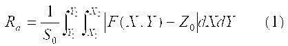
여기서, 지정면이란 조도 계측의 대상이 되는 면이며, 좌표(X1, Y1)(X1, Y2)(X2, Y1)(X2, Y2)로 나타나는 4점에 의해 둘러싸이는 직사각형의 영역으로 하고, 지정면이 이상적으로 플랫하다고 한 때의 면적을 S0으로 한다. 또한, 기준면이란 지정면의 평균 높이에 있어서의 XY 평면과 평행한 면을 말한다. 즉, 지정면의 높이의 평균값을 Z0으로 할 때, 기준면의 높이도 Z0으로 나타난다. 평균면 조도(Ra)는 원자간력현미경(AFM: Atomic Force Microscope)으로 평가 가능하다.Here, the designated surface is a surface to be subjected to roughness measurement, and is surrounded by four points represented by coordinates (X 1 , Y 1 ) (X 1 , Y 2 ) (X 2 , Y 1 ) (X 2 , Y 2 ). to the area of a rectangle, and when the area of the designating area that is ideally flat with S 0. In addition, a reference plane means the surface parallel to the XY plane in the average height of a designation surface. In other words, when the average value of the height of the designated surface is Z 0 , the height of the reference surface is also represented by Z 0 . Average surface roughness (Ra) can be assessed by Atomic Force Microscope (AFM).
상기 CMP 처리는 1회 수행할 수도 있고, 복수 회 수행할 수도 있다. 복수 회로 나누어 CMP 처리를 수행하는 경우는 높은 연마 레이트의 1차 연마를 수행한 후, 낮은 연마 레이트의 마무리 연마를 수행하는 것이 바람직하다. 이와 같이 연마 레이트가 다른 연마를 조합함으로써 절연막(225)의 표면의 평탄성을 더욱 향상시킬 수 있다.The CMP process may be performed once or plural times. In the case where the CMP treatment is divided into a plurality of circuits, it is preferable to perform high polishing rate primary polishing, and then perform low polishing rate finish polishing. By combining the polishing with different polishing rates in this manner, the flatness of the surface of the insulating
또한, 절연막(225)을 평탄화시키는 처리로서는, 플라즈마 처리를 이용할 수도 있다. 플라즈마 처리는 진공의 챔버에 불활성 가스, 예를 들어 아르곤 가스 등의 희가스를 도입하고, 피처리면을 음극으로 하는 전계를 인가하여 수행한다. 그 원리는 플라즈마 드라이 에칭법과 동등하지만, 불활성 가스를 이용하여 수행한다. 즉, 이 플라즈마 처리는 피처리면에 불활성 가스의 이온을 조사하여, 스퍼터링 효과에 의해 표면의 미세한 요철을 평탄화하는 처리이다. 그러므로, 이 플라즈마 처리를 「역스퍼터 처리」라고 부를 수도 있다.As the treatment for flattening the insulating
이 플라즈마 처리 시, 플라즈마 내에는 전자와 아르곤의 양이온이 존재하고, 음극 방향으로 아르곤의 양이온이 가속된다. 가속된 아르곤의 양이온은 피처리면을 스퍼터한다. 이때, 그 피처리면의 볼록부부터 우선적으로 스퍼터된다. 피처리면으로부터 스퍼터된 입자는 피처리면의 다른 곳에 부착된다. 이때, 그 피처리면의 오목부에 우선적으로 부착된다. 이와 같이 볼록부를 깎고 오목부를 메움으로써 피처리면의 평탄성이 향상한다. 또한, 플라즈마 처리와 CMP 처리를 병용함으로써 더욱 절연막(225)의 평탄화를 도모할 수 있다.During this plasma treatment, cations of electrons and argon exist in the plasma, and cations of argon are accelerated toward the cathode. Accelerated argon cations sputter the surface to be treated. At this time, it is sputtered preferentially from the convex part of the to-be-processed surface. Particles sputtered from the surface to be treated are attached elsewhere on the surface to be treated. At this time, it attaches preferentially to the recessed part of the to-be-processed surface. Thus, the flatness of the to-be-processed surface improves by cutting out a convex part and filling a recessed part. In addition, by using the plasma process and the CMP process together, the insulating
또한, 이 플라즈마 처리에 의해, 절연막(225) 표면에 부착된 수분, 유기물 등의 불순물을 스퍼터링의 효과로 제거하는 것도 가능하다.In addition, by this plasma treatment, impurities such as moisture, organic matter and the like deposited on the surface of the insulating
또한, 산화물 반도체의 성막을 수행하기 전에 처리실의 가열 및 배기를 수행하여, 처리실 내의 수소, 물, 수산기, 수소화물 등의 불순물을 제거해 두는 것이 바람직하다. 특히 처리실의 내벽에 흡착해 존재하는 이들 불순물을 제거하는 것이 중요하다. 여기서, 가열 처리는 예를 들어, 100℃ 이상 450℃ 이하로 수행할 수 있다. 또한, 처리실의 배기는 드라이 펌프 등의 저진공 펌프와, 스퍼터 이온 펌프, 터보 분자 펌프 및 크라이오 펌프 등의 고진공 펌프를 적절히 조합하여 수행하면 된다. 터보 분자 펌프는 큰 사이즈의 분자의 배기가 우수한 반면, 수소나 물의 배기 능력이 낮다. 나아가, 터보 분자 펌프와, 물의 배기 능력이 높은 크라이오 펌프 또는 수소의 배기 능력이 높은 스퍼터 이온 펌프를 조합시키는 것이 유효하다. 또한 이때 불활성 가스를 도입하면서 불순물의 제거를 수행하면, 배기하는 것 만으로는 탈리하기 어려운 물 등의 탈리 속도를 더욱 크게 할 수 있다. 이러한 처리를 수행하여 산화물 반도체의 성막 전에 처리실의 불순물을 제거함으로써, 산화물 반도체에의 수소, 물, 수산기, 수소화물 등의 혼입을 저감시킬 수 있다.In addition, it is preferable to remove the impurities such as hydrogen, water, hydroxyl groups, and hydride in the processing chamber by heating and evacuating the processing chamber before forming the oxide semiconductor. In particular, it is important to remove these impurities which are adsorbed on the inner wall of the processing chamber. Here, heat processing can be performed, for example at 100 degreeC or more and 450 degrees C or less. In addition, the evacuation of the processing chamber may be performed by appropriately combining a low vacuum pump such as a dry pump and a high vacuum pump such as a sputter ion pump, a turbo molecular pump, and a cryopump. Turbomolecular pumps are good at exhausting large sized molecules, but have low capacity for hydrogen or water. Furthermore, it is effective to combine a turbo molecular pump with a cryopump having a high water exhaust capacity or a sputter ion pump having a high exhaust capacity of hydrogen. In addition, if impurities are removed while introducing an inert gas at this time, the desorption rate of water or the like that is difficult to be removed simply by evacuation can be further increased. By performing such a treatment to remove impurities in the processing chamber prior to film formation of the oxide semiconductor, the incorporation of hydrogen, water, hydroxyl groups, hydrides, and the like into the oxide semiconductor can be reduced.
또한, 산화물 반도체막을 스퍼터링 장치로 성막하기 전에, 스퍼터링 장치에 더미 기판을 반입하고, 더미 기판 상에 산화물 반도체막을 성막하여, 타겟 표면 또는 방착판에 부착된 수소, 수분을 제거하는 공정을 수행할 수도 있다.In addition, before depositing the oxide semiconductor film with the sputtering apparatus, a dummy substrate may be loaded into the sputtering apparatus, and an oxide semiconductor film is formed on the dummy substrate to remove hydrogen and moisture adhering to the target surface or the deposition plate. have.
이어서, 절연막(225) 상에 스퍼터링법, 도포법, 인쇄법, 펄스 레이저 증착법 등을 이용하여 산화물 반도체막(227)을 형성한다(도 5(B) 참조.). 여기서는, 산화물 반도체막(227)으로서, 스퍼터링법에 의해 1nm 이상 50nm 이하, 더욱 바람직하게는 3nm 이상 30nm 이하의 두께로 산화물 반도체막을 형성한다. 산화물 반도체막(227)의 두께를 상기 두께로 함으로써, 트랜지스터의 미세화에 수반하여 발생할 우려가 있는 쇼트 채널 효과를 억제할 수 있다.Next, an
산화물 반도체막(227)에 이용하는 산화물 반도체로서는 적어도 인듐(In) 또는 아연(Zn)을 포함하는 것이 바람직하다. 특히 In과 Zn을 포함하는 것이 바람직하다. 또한, 그 산화물 반도체를 이용한 트랜지스터의 전기 특성의 편차를 줄이기 위한 스태빌라이저로서 그것들에 추가로 갈륨(Ga)을 갖는 것이 바람직하다. 또한, 스태빌라이저로서 주석(Sn)을 갖는 것이 바람직하다. 또한, 스태빌라이저로서 하프늄(Hf)을 갖는 것이 바람직하다. 또한, 스태빌라이저로서 알루미늄(Al)을 갖는 것이 바람직하다.As the oxide semiconductor used for the
또한, 그 외의 스태빌라이저로서, 란타노이드인 란탄(La), 세륨(Ce), 프라세오디뮴(Rr), 네오디뮴(Nd), 사마륨(Sm), 유로퓸(Eu), 가돌리늄(Gd), 테르븀(Tb), 디스프로슘(Dy), 홀뮴(Ho), 에르븀(Er), 툴륨(Tm), 이테르븀(Yb), 루테튬(Lu) 중 어느 1종 또는 복수 종을 가질 수도 있다.In addition, as other stabilizers, lanthanide (La), cerium (Ce), praseodymium (Rr), neodymium (Nd), samarium (Sm), europium (Eu), gadolinium (Gd), terbium (Tb), It may have any one kind or plural kinds of dysprosium (Dy), holmium (Ho), erbium (Er), thulium (Tm), ytterbium (Yb) and lutetium (Lu).
예를 들어, 산화물 반도체로서, 산화 인듐, 산화 주석, 산화 아연, 2원계 금속 산화물인 In-Zn계 산화물, Sn-Zn계 산화물, Al-Zn계 산화물, Zn-Mg계 산화물, Sn-Mg계 산화물, In-Mg계 산화물, In-Ga계 산화물, 3원계 금속 산화물인 In-Ga-Zn계 산화물(IGZO라고도 표기함), In-Al-Zn계 산화물, In-Sn-Zn계 산화물, Sn-Ga-Zn계 산화물, Al-Ga-Zn계 산화물, Sn-Al-Zn계 산화물, In-Hf-Zn계 산화물, In-La-Zn계 산화물, In-Ce-Zn계 산화물, In-Pr-Zn계 산화물, In-Nd-Zn계 산화물, In-Sm-Zn계 산화물, In-Eu-Zn계 산화물, In-Gd-Zn계 산화물, In-Tb-Zn계 산화물, In-Dy-Zn계 산화물, In-Ho-Zn계 산화물, In-Er-Zn계 산화물, In-Tm-Zn계 산화물, In-Yb-Zn계 산화물, In-Lu-Zn계 산화물, 4원계 금속 산화물인 In-Sn-Ga-Zn계 산화물, In-Hf-Ga-Zn계 산화물, In-Al-Ga-Zn계 산화물, In-Sn-Al-Zn계 산화물, In-Sn-Hf-Zn계 산화물, In-Hf-Al-Zn계 산화물을 이용할 수 있다. 또한, 상기 산화물 반도체에 산화 실리콘을 포함할 수도 있다. 여기서, 예를 들어, In-Ga-Zn계 산화물이란, 인듐(In), 갈륨(Ga), 아연(Zn)을 주성분으로서 갖는 산화물이라는 의미이며, In과 Ga와 Zn의 비율은 문제시 하지 않는다. 또한, In과 Ga와 Zn 이외의 금속 원소가 들어가 있어도 된다. 이때, 상기 산화물 반도체에 있어서는 화학양론비에 대해 산소를 과잉으로 하면 바람직하다. 산소를 과잉으로 함으로써 산화물 반도체막의 산소 결손에 기인하는 캐리어의 생성을 억제할 수 있다.For example, indium oxide, tin oxide, zinc oxide, In-Zn-based oxides, Sn-Zn-based oxides, Al-Zn-based oxides, Zn-Mg-based oxides, Sn-Mg-based oxides as oxide semiconductors Oxides, In-Mg oxides, In-Ga oxides, In-Ga-Zn oxides (also referred to as IGZOs), ternary metal oxides, In-Al-Zn oxides, In-Sn-Zn oxides, Sn -Ga-Zn oxide, Al-Ga-Zn oxide, Sn-Al-Zn oxide, In-Hf-Zn oxide, In-La-Zn oxide, In-Ce-Zn oxide, In-Pr -Zn oxide, In-Nd-Zn oxide, In-Sm-Zn oxide, In-Eu-Zn oxide, In-Gd-Zn oxide, In-Tb-Zn oxide, In-Dy-Zn In-Ho-Zn oxide, In-Er-Zn oxide, In-Tm-Zn oxide, In-Yb-Zn oxide, In-Lu-Zn oxide, In- Sn-Ga-Zn oxide, In-Hf-Ga-Zn oxide, In-Al-Ga-Zn oxide, In-Sn-Al-Zn oxide, In-Sn-Hf-Zn oxide, In- Hf-Al-Zn type oxide can be used. Further, silicon oxide may be included in the oxide semiconductor. Here, for example, an In—Ga—Zn-based oxide means an oxide having indium (In), gallium (Ga), and zinc (Zn) as main components, and the ratio of In, Ga, and Zn does not matter. . In addition, metallic elements other than In, Ga, and Zn may be contained. At this time, in the oxide semiconductor, it is preferable to make oxygen excessive with respect to the stoichiometric ratio. By making oxygen excess, generation | occurrence | production of the carrier resulting from the oxygen deficiency of an oxide semiconductor film can be suppressed.
또한, 산화물 반도체로서 InMO3(ZnO)m(m>0, 또한 m은 정수가 아님)으로 표기되는 재료를 이용할 수도 있다. 또한, M은 Ga, Fe, Mn 및 Co로부터 선택된 하나의 금속 원소 또는 복수의 금속 원소를 나타낸다. 또한, 산화물 반도체로서 In3SnO5(ZnO)n(n>0, 또한 n은 정수)으로 표기되는 재료를 이용할 수도 있다.As the oxide semiconductor, a material denoted by InMO 3 (ZnO) m (m> 0, and m is not an integer) may be used. In addition, M represents one metal element or a plurality of metal elements selected from Ga, Fe, Mn and Co. As the oxide semiconductor, a material represented by In 3 SnO 5 (ZnO) n (n> 0, where n is an integer) may be used.
또한, 산화물 반도체막(227)에 있어서 알칼리 금속 또는 알칼리 토류 금속의 농도는 1×10¹⁸atoms/㎤ 이하, 더욱 바람직하게는 2×10¹⁶atoms/㎤ 이하인 것이 바람직하다. 알칼리 금속 및 알칼리 토류 금속은 산화물 반도체와 결합하면 캐리어가 생성될 수 있어, 트랜지스터의 오프 전류의 상승의 원인이 되기 때문이다.The concentration of the alkali metal or alkaline earth metal in the
또한, 산화물 반도체막(227)에는 5×10¹⁸atoms/㎤ 이하의 질소가 포함되어 있을 수도 있다.In addition, the
또한, 산화물 반도체막(227)에 이용하는 것이 가능한 산화물 반도체는 실리콘 반도체보다 밴드갭이 넓고, 진성 캐리어 밀도가 실리콘보다 작은 와이드 밴드갭 반도체로 한다. 이와 같이, 밴드갭이 넓은 산화물 반도체를 이용함으로써, 트랜지스터의 오프 전류를 저감시킬 수 있다.The oxide semiconductor that can be used for the
산화물 반도체막(227)은 단결정 구조일 수도 있고, 비단결정 구조일 수도 있다. 후자의 경우, 아몰퍼스 구조 또는 다결정 구조일 수도 있다. 또한, 아몰퍼스 내에 결정성을 갖는 부분을 포함하는 구조 또는 비아몰퍼스 구조일 수도 있다.The
아몰퍼스 상태의 산화물 반도체는 비교적 용이하게 평탄한 표면을 얻을 수 있으므로, 이를 이용하여 트랜지스터를 제작했을 시의 계면산란을 저감시킬 수 있고, 비교적 용이하게 비교적 높은 이동도를 얻을 수 있다.Since the oxide semiconductor in the amorphous state can obtain a flat surface relatively easily, the interfacial scattering when the transistor is fabricated using this can be reduced, and relatively high mobility can be obtained relatively easily.
또한, 결정성을 갖는 산화물 반도체에서는 벌크 내 결함을 보다 저감할 수 있고, 표면의 평탄성을 높이면 아몰퍼스 상태의 산화물 반도체 이상의 이동도를 얻을 수 있다. 표면의 평탄성을 높이기 위해서는, 평탄한 표면 상에 산화물 반도체를 형성하는 것이 바람직하고, 상술한 바와 같이, 절연막(225)의 표면의 평균면 조도(Ra)를 1nm 이하, 바람직하게는 0.3nm 이하, 보다 바람직하게는 0.1nm 이하로 하고, 그 위에 산화물 반도체막(227)을 형성하는 것이 바람직하다.In addition, in the oxide semiconductor having crystallinity, defects in bulk can be further reduced, and the mobility of the oxide semiconductor in an amorphous state can be obtained by increasing the flatness of the surface. In order to increase the flatness of the surface, it is preferable to form an oxide semiconductor on the flat surface. As described above, the average surface roughness Ra of the surface of the insulating
여기서는, 산화물 반도체막(227)을 스퍼터링법에 의해 형성한다.Here, the
스퍼터링법에 이용하는 타겟으로서는, 예를 들어, 산화 인듐, 산화 주석, 산화 아연, 2원계 금속 산화물인 In-Zn계 산화물, Sn-Zn계 산화물, Al-Zn계 산화물, Zn-Mg계 산화물, Sn-Mg계 산화물, In-Mg계 산화물, In-Ga계 산화물, 3원계 금속 산화물인 In-Ga-Zn계 산화물(IGZO라고도 표기함), In-Al-Zn계 산화물, In-Sn-Zn계 산화물, Sn-Ga-Zn계 산화물, Al-Ga-Zn계 산화물, Sn-Al-Zn계 산화물, In-Hf-Zn계 산화물, In-La-Zn계 산화물, In-Ce-Zn계 산화물, In-Pr-Zn계 산화물, In-Nd-Zn계 산화물, In-Sm-Zn계 산화물, In-Eu-Zn계 산화물, In-Gd-Zn계 산화물, In-Tb-Zn계 산화물, In-Dy-Zn계 산화물, In-Ho-Zn계 산화물, In-Er-Zn계 산화물, In-Tm-Zn계 산화물, In-Yb-Zn계 산화물, In-Lu-Zn계 산화물, 4원계 금속 산화물인 In-Sn-Ga-Zn계 산화물, In-Hf-Ga-Zn계 산화물, In-Al-Ga-Zn계 산화물, In-Sn-Al-Zn계 산화물, In-Sn-Hf-Zn계 산화물, In-Hf-Al-Zn계 산화물을 이용할 수 있다.As a target used for a sputtering method, for example, indium oxide, tin oxide, zinc oxide, an In-Zn oxide which is a binary metal oxide, Sn-Zn oxide, Al-Zn oxide, Zn-Mg oxide, Sn -Mg oxide, In-Mg oxide, In-Ga oxide, In-Ga-Zn oxide (also referred to as IGZO), a ternary metal oxide, In-Al-Zn oxide, In-Sn-Zn Oxides, Sn-Ga-Zn oxides, Al-Ga-Zn oxides, Sn-Al-Zn oxides, In-Hf-Zn oxides, In-La-Zn oxides, In-Ce-Zn oxides, In-Pr-Zn oxide, In-Nd-Zn oxide, In-Sm-Zn oxide, In-Eu-Zn oxide, In-Gd-Zn oxide, In-Tb-Zn oxide, In- Dy-Zn oxide, In-Ho-Zn oxide, In-Er-Zn oxide, In-Tm-Zn oxide, In-Yb-Zn oxide, In-Lu-Zn oxide, quaternary metal oxide Phosphorus In-Sn-Ga-Zn-based oxide, In-Hf-Ga-Zn-based oxide, In-Al-Ga-Zn-based oxide, In-Sn-Al-Zn-based oxide, In-Sn-Hf-Zn-based oxide , In-Hf-Al-Zn-based oxide It can be used.
산화물 반도체로서 In-Ga-Zn-O계의 재료를 사용하는 경우, 사용하는 타겟의 조성비는 예를 들어, 원자수비로 In:Ga:Zn=1:1:1(=1/3:1/3:1/3)(몰수비로 환산하면 In2O3:Ga2O3:ZnO=1:1:2), In:Ga:Zn=2:2:1(=2/5:2/5:1/5)(몰수비로 환산하면 In2O3:Ga2O3:ZnO=1:1:1) 등일 수 있다. 이와 같은 원자수비의 In-Ga-Zn계 산화물이나 그 조성의 근방의 산화물을 타겟으로서 사용할 수 있다.In the case of using an In-Ga-Zn-O-based material as the oxide semiconductor, the composition ratio of the target to be used is, for example, In: Ga: Zn = 1: 1: 1 (= 1/3: 1 / 3: 1/3) (In molar ratio, In2O3: Ga2O3: ZnO = 1: 1: 2), In: Ga: Zn = 2: 2: 1 (= 2/5: 2/5: 1/5) ( In terms of the molar ratio, In2O3: Ga2O3: ZnO = 1: 1: 1) may be used. Such atomic ratio In-Ga-Zn-based oxides and oxides in the vicinity of the composition can be used as targets.
또한, 산화물 반도체로서 In-Sn-Zn-O계의 재료를 사용하는 경우, 사용하는 타겟의 조성비는 예를 들어, 원자수비로 In:Sn:Zn=1:1:1(=1/3:1/3:1/3), In:Sn:Zn=2:1:3(=1/3:1/6:1/2), In:Sn:Zn=2:1:5(=1/4:1/8:5/8, In:Sn:Zn=1:2:2(=1/5:2/5:2/5), In:Sn:Zn=20:45:35 등일 수 있다. 이와 같은 원자수비의 In-Sn-Zn계 산화물이나 그 조성의 근방의 산화물을 타겟으로서 사용할 수 있다.In the case of using an In—Sn—Zn—O-based material as the oxide semiconductor, the composition ratio of the target to be used is, for example, In: Sn: Zn = 1: 1: 1 (= 1/3: 1/3: 1/3), In: Sn: Zn = 2: 1: 3 (= 1/3: 1/6: 1/2), In: Sn: Zn = 2: 1: 5 (= 1 / 4: 1/8: 5/8, In: Sn: Zn = 1: 2: 2 (= 1/5: 2/5: 2/5), In: Sn: Zn = 20: 45: 35 and the like. Such atomic ratio In-Sn-Zn-based oxides and oxides in the vicinity of the composition can be used as targets.
산화물 반도체로서 In-Zn-O계의 재료를 사용하는 경우, 사용하는 타겟의 조성비는 원자수비로 In:Zn=50:1~1:2(몰수비로 환산하면 In2O3:ZnO=25:1~1:4), 바람직하게는 In:Zn=20:1~1:1(몰수비로 환산하면 In2O3:ZnO=10:1~1:2), 더욱 바람직하게는 In:Zn=15:1~1.5:1(몰수비로 환산하면 In2O3:ZnO=15:2~3:4)로 한다. 예를 들어, In-Zn-O계 산화물 반도체의 형성에 사용하는 타겟은 원자수비가 In:Zn:O=X:Y:Z일 때, Z>1.5X+Y로 한다. 이와 같은 원자수비의 In-Zn-O계 산화물이나 그 조성 근방의 산화물을 타겟으로서 사용할 수 있다.In the case of using an In—Zn—O-based material as an oxide semiconductor, the composition ratio of the target to be used is In: Zn = 50: 1 to 1: 2 in atomic ratio (In 2 O 3 : ZnO = 25: 1 to 1: 4), preferably In: Zn = 20: 1 to 1: 1 (In 2 O 3 : ZnO = 10: 1 to 1: 2 in terms of molar ratio), and more preferably In: Zn = 15: 1 ~ 1.5: 1 (In terms of molar ratio, In 2 O 3 : ZnO = 15: 2 ~ 3: 4). For example, the target used for forming an In—Zn—O based oxide semiconductor is Z> 1.5X + Y when the atomic ratio is In: Zn: O = X: Y: Z. Such atomic ratio In-Zn-O-based oxides and oxides near its composition can be used as targets.
그러나, 이들에 한정되지 않으며, 필요로 하는 반도체 특성(이동도, 문턱값, 편차 등)에 따라 적절한 조성의 것을 사용하면 된다. 또한, 필요로 하는 반도체 특성을 얻기 위해서 캐리어 농도나 불순물 농도, 결함밀도, 금속 원소와 산소의 원자수비, 원자간 결합 거리, 밀도 등을 적절한 것으로 하는 것이 바람직하다.However, it is not limited to these, What is necessary is just to use the thing of a suitable composition according to the semiconductor characteristic (mobility, a threshold value, a deviation, etc.) required. In addition, in order to obtain the required semiconductor characteristics, it is preferable to set the carrier concentration, the impurity concentration, the defect density, the atomic ratio of the metal element and oxygen, the bond distance between atoms, the density, and the like as appropriate.
예를 들어, In-Sn-Zn계 산화물에서는 비교적 용이하게 높은 이동도가 얻어진다. 그러나, In-Ga-Zn계 산화물에서도 벌크 내 결함밀도를 저감시킴으로써 이동도를 높일 수 있다.For example, in In—Sn—Zn-based oxides, high mobility can be obtained relatively easily. However, even in In-Ga-Zn-based oxides, mobility can be increased by reducing the defect density in bulk.
또한, 예를 들어, In, Ga, Zn의 원자수비가 In:Ga:Zn=a:b:c(a+b+c=1)인 산화물의 조성이, 원자수비가 In:Ga:Zn=A:B:C(A+B+C=1)인 산화물의 조성의 근방이라는 것은 a, b, c가 (a-A)2 +(b-B)2 +(c-C)2≤r2를 충족시키는 것을 말하며, r은 예를 들어 0.05일 수 있다. 다른 산화물에서도 마찬가지이다.For example, the composition of the oxide whose atomic ratio of In, Ga, Zn is In: Ga: Zn = a: b: c (a + b + c = 1) has the atomic ratio In: Ga: Zn = A: B: The vicinity of the composition of the oxide of C (A + B + C = 1) means that a, b and c satisfy (aA) 2 + (bB) 2 + (cC) 2 ≤ r 2 , where r is, for example, 0.05 days. Can be. The same is true for other oxides.
또한, 스퍼터링 가스는 희가스(대표적으로는 아르곤) 분위기, 산소 분위기, 희가스 및 산소의 혼합 가스를 적절히 사용한다. 아울러, 희가스 및 산소의 혼합 가스의 경우, 희가스에 대해 산소의 가스비를 높이는 것이 바람직하다. 또한, 스퍼터링 가스는 산화물 반도체막에의 수소, 물, 수산기, 수소화물 등의 혼입을 방지하기 위해서, 수소, 물, 수산기, 수소화물 등의 불순물이 충분히 제거된 고순도 가스를 사용한 분위기로 하는 것이 바람직하다.As the sputtering gas, a rare gas (typically argon) atmosphere, an oxygen atmosphere, a rare gas and a mixed gas of oxygen are suitably used. In addition, in the case of the mixed gas of a rare gas and oxygen, it is preferable to raise the gas ratio of oxygen with respect to a rare gas. In addition, in order to prevent mixing of hydrogen, water, hydroxyl groups, and hydrides into the oxide semiconductor film, the sputtering gas is preferably an atmosphere using a high-purity gas in which impurities such as hydrogen, water, hydroxyl groups, and hydrides are sufficiently removed. Do.
스퍼터링법에 있어서, 플라즈마를 발생시키기 위한 전원장치는 RF 전원장치, AC 전원장치, DC 전원장치 등을 적절히 사용할 수 있다.In the sputtering method, a power supply device for generating plasma can be suitably used an RF power supply device, an AC power supply device, a DC power supply device, or the like.
또한, 산화물 반도체막을 성막하는 처리실은 리크 레이트를 1×10⁻¹⁰Pa?㎥/초 이하로 하는 것이 바람직하며, 이에 따라 스퍼터링법에 의해 성막할 시 막 내로의 불순물의 혼입을 저감시킬 수 있다. 이와 같이, 산화물 반도체막의 성막 공정에서, 더욱 바람직하게는 산화 절연막의 성막 공정에서, 처리실의 압력, 처리실의 리크 레이트 등에 있어서 불순물의 혼입을 가능한 한 억제함으로써, 산화물 반도체막에 포함되는 수소를 포함하는 불순물의 혼입을 저감시킬 수 있다. 또한, 산화 절연막으로부터 산화물 반도체막에의 수소 등의 불순물의 확산을 저감시킬 수 있다.In addition, the process chamber for forming the oxide semiconductor film preferably has a leak rate of 1 × 10 −10 Pa ·
또한, 산화물 반도체막(227)으로서 CAAC-OS(C Axis Aligned Crystalline Oxide Semiconductor)막을 이용할 수도 있다.Further, a CAAC-OS (C Axis Aligned Crystalline Oxide Semiconductor) film may be used as the
CAAC-OS란, c축 배향하고, 또한 ab면, 표면 또는 계면의 방향으로부터 보아 삼각형상 또는 육각형상의 원자배열을 가지며, c축에 있어서는, 금속원자가 층상으로 또는 금속원자와 산소원자가 층상으로 배열해 있고, ab면(또는 표면 또는 계면)에 있어서는, a축 또는 b축의 방향이 다른(c축을 중심으로 회전한) 결정을 포함하는 산화물 반도체이다.CAAC-OS has a c-axis orientation and has a triangular or hexagonal atomic arrangement as viewed from the ab plane, surface or interface direction. In the c-axis, metal atoms are arranged in layers or metal atoms and oxygen atoms are arranged in layers. In the ab plane (or the surface or the interface), the oxide semiconductor contains crystals (rotated about the c-axis) that are different in the a-axis or b-axis direction.
넓은 의미에서 CAAC-OS란 비단결정이며, 그 ab면에 수직인 방향으로부터 보아, 삼각형 혹은 육각형, 또는 정삼각형 혹은 정육각형의 원자 배열을 가지며, 또한 c축 방향으로 수직인 방향으로부터 보아 금속원자가 층상으로 또는 금속원자와 산소원자가 층상으로 배열한 상을 포함하는 산화물 반도체를 말한다.In a broad sense, CAAC-OS is a non-single crystal and has an atomic arrangement of triangles or hexagons, or equilateral triangles or hexagons, as viewed from the direction perpendicular to its ab plane, and metal atoms in layers or as viewed from the direction perpendicular to the c-axis direction. An oxide semiconductor comprising a phase in which metal atoms and oxygen atoms are arranged in a layered manner.
CAAC-OS는 단결정은 아니지만, 비정질만으로 형성되어 있는 것도 아니다. 또한, CAAC-OS는 결정화한 부분(결정 부분)을 포함하지만, 하나의 결정 부분과 다른 결정 부분의 경계를 명확하게 판별할 수 없는 경우도 있다.Although CAAC-OS is not a single crystal, it is not formed by only amorphous. In addition, although the CAAC-OS includes a crystallized portion (crystal portion), in some cases, the boundary between one crystal portion and another crystal portion cannot be clearly determined.
CAAC-OS를 구성하는 산소의 일부는 질소로 치환될 수도 있다. 또한, CAAC-OS를 구성하는 개개의 결정 부분의 c축은 일정한 방향(예를 들어, CAAC-OS를 형성하는 기판면이나 CAAC-OS의 표면이나 막면, 계면 등에 수직인 방향)으로 일치되어 있어도 된다. 또는, CAAC-OS를 구성하는 개개의 결정 부분의 ab면의 법선은 일정한 방향(예를 들어, 기판면, 표면, 막면, 계면 등에 수직인 방향)을 향하고 있어도 된다.Some of the oxygen constituting the CAAC-OS may be substituted with nitrogen. In addition, the c-axis of the individual crystal parts constituting the CAAC-OS may coincide in a predetermined direction (for example, a direction perpendicular to the surface of the substrate forming the CAAC-OS, the surface of the CAAC-OS, the film, or the interface). . Alternatively, the normal line of the ab planes of the individual crystal parts constituting the CAAC-OS may be directed in a constant direction (for example, a direction perpendicular to the substrate plane, the surface, the film plane, the interface, and the like).
이러한 c축 배향을 갖는 결정을 포함하는 산화물 반도체막을 마련함으로써, 가시광이나 자외광의 조사에 의한 전기적 특성의 변화를 억제할 수 있다. 특히, 상술한 바와 같이, 절연막(225)의 표면의 평균면 조도(Ra)를 1nm 이하, 바람직하게는 0.3nm 이하, 보다 바람직하게는 0.1nm 이하로 하고, 그 위에 c축 배향을 갖는 결정을 포함하는 산화물 반도체막을 형성하는 것이 바람직하다. 이에 따라, c축 배향을 갖는 결정을 포함하는 산화물 반도체막의 결정성을 향상시켜, 이 산화물 반도체막을 이용한 트랜지스터의 이동도의 향상을 도모할 수 있다.By providing the oxide semiconductor film containing the crystal | crystallization which has such a c-axis orientation, the change of the electrical characteristic by irradiation of visible light or an ultraviolet light can be suppressed. In particular, as described above, the average surface roughness Ra of the surface of the insulating
CAAC-OS에 포함되는 결정 구조의 일례에 대해서 도 10 내지 도 12를 이용하여 상세하게 설명한다. 또한, 특별히 언급이 없는 한, 도 10 내지 도 12는 상방향을 c축 방향으로 하고, c축 방향과 직교하는 면을 ab면으로 한다. 또한, 단순히 상반분, 하반분이라고 하는 경우, ab면을 경계로 했을 경우의 상반분, 하반분을 말한다. 또한, 도 10에서 동그라미로 둘러싸인 O는 4배위의 O를 나타내고, 이중 동그라미로 둘러싸인 O는 3배위의 O를 나타낸다.An example of the crystal structure included in the CAAC-OS will be described in detail with reference to FIGS. 10 to 12. In addition, unless otherwise indicated, FIGS. 10-12 make an upper direction into a c-axis direction, and makes the surface orthogonal to a c-axis direction ab plane. In the case of simply referred to as the upper half and the lower half, the upper half and the lower half when the ab plane is the boundary. In FIG. 10, O enclosed in circles represents O in four coordination, and O enclosed in double circles represents O in three coordination.
도 10(A)에, 1개의 6배위의 In과, In에 근접한 6개의 4배위의 산소원자(이하 4배위의 O)를 갖는 구조를 나타낸다. 여기서는, 금속원자 1개에 대하여, 근접한 산소원자만 나타낸 구조를 소그룹이라고 부른다. 도 10(A)의 구조는 팔면체 구조를 하고 있으나, 간단화를 위해 평면 구조로 나타내고 있다. 또한, 도 10(A)의 상반분 및 하반분에는 각각 3개씩 4배위의 O가 있다. 도 10(A)에 나타내는 소그룹은 전하가 0이다.10 (A), the structure which has one 6 coordination In and six 4 coordination oxygen atoms (O of 4 coordination hereafter) adjacent to In is shown. Here, a structure in which only oxygen atoms are adjacent to one metal atom is called a small group. Although the structure of FIG. 10A has an octahedral structure, it is shown by the planar structure for simplicity. In addition, in the upper half and the lower half of FIG. The small group shown in Fig. 10A has zero charge.
도 10(B)에, 1개의 5배위의 Ga와, Ga에 근접한 3개의 3배위의 산소원자(이하 3배위의 O)와, Ga에 근접한 2개의 4배위의 O를 갖는 구조를 나타낸다. 3배위의 O는 모두 ab면에 존재한다. 도 10(B)의 상반분 및 하반분에는 각각 1개씩 4배위의 O가 있다. 또한, In도 5배위를 취하기 때문에, 도 10(B)에 나타내는 구조를 취할 수 있다. 도 10(B)에 나타내는 소그룹은 전하가 0이다.10B shows a structure having one 5 coordination Ga, three triple coordination oxygen atoms (hereinafter, three coordination O) close to Ga, and two quadrangles O close to Ga. All three coordination O is on the ab plane. In the upper half and the lower half of FIG. Since In also takes 5 coordination, the structure shown in FIG. 10 (B) can be taken. The small group shown in Fig. 10B has zero charge.
도 10(C)에, 1개의 4배위의 Zn과, Zn에 근접한 4개의 4배위의 O를 갖는 구조를 나타낸다. 도 10(C)의 상반분에는 1개의 4배위의 O가 있고, 하반분에는 3개의 4배위의 O가 있다. 또는, 도 10(C)의 상반분에 3개의 4배위의 O가 있고, 하반분에 1개의 4배위의 O가 있을 수도 있다. 도 10(C)에 나타내는 소그룹은 전하가 0이다.10C shows a structure having one quadruple Zn and four quadratic O close to Zn. In the upper half of Fig. 10C, there is one quadrant of O, and in the lower half there are three quarters of O. Alternatively, there may be three quadrangles of O in the upper half of FIG. 10 (C), and one quadrant of O in the lower half. The small group shown in Fig. 10C has zero charge.
도 10(D)에, 1개의 6배위의 Sn과, Sn에 근접한 6개의 4배위의 O를 갖는 구조를 나타낸다. 도 10(D)의 상반분에는 3개의 4배위의 O가 있고, 하반분에는 3개의 4배위의 O가 있다. 도 10(D)에 나타내는 소그룹은 전하가 +1이 된다.10D shows a structure having one six coordinating Sn and six four coordinating O close to Sn. In the upper half of Fig. 10 (D), there are three quadruples of O, and in the lower half there are three quarters of O. In the small group shown in Fig. 10D, the charge becomes +1.
도 10(E)에, 2개의 Zn을 포함하는 소그룹을 나타낸다. 도 10(E)의 상반분에는 1개의 4배위의 O가 있고, 하반분에는 1개의 4배위의 O가 있다. 도 10(E)에 나타내는 소그룹은 전하가 -1이 된다.10 (E) shows a small group containing two Zn. In the upper half of Fig. 10E, there is one quadrant of O, and in the lower half there is one quadrant of O. In the small group shown in Fig. 10E, the charge becomes -1.
여기서는, 복수의 소그룹의 집합체를 중그룹이라고 부르고, 복수의 중그룹의 집합체를 대그룹(유닛 셀이라고도 함.)이라고 부른다.Here, an aggregate of a plurality of small groups is called a medium group, and an aggregate of a plurality of medium groups is called a large group (also called a unit cell).
여기서, 이들 소그룹끼리가 결합하는 규칙에 대해서 설명한다. 도 10(A)에 나타내는 6배위의 In의 상반분의 3개의 O는 하방향에 각각 3개의 근접 In을 갖고, 하반분의 3개의 O는 상방향에 각각 3개의 근접 In을 갖는다. 도 10(B)에 나타내는 5배위의 Ga의 상반분의 1개의 O는 하방향에 1개의 근접 Ga를 갖고, 하반분의 1개의 O는 상방향에 1개의 근접 Ga를 갖는다. 도 10(C)에 나타내는 4배위의 Zn의 상반분의 1개의 O는 하방향에 1개의 근접 Zn을 갖고, 하반분의 3개의 O는 상방향에 각각 3개의 근접 Zn을 갖는다. 이와 같이, 금속원자의 상방향의 4배위의 O의 수와, 그 O의 하방향에 있는 근접 금속원자의 수는 동일하고, 마찬가지로 금속원자의 하방향의 4배위의 O의 수와, 그 O의 상방향에 있는 근접 금속원자의 수는 동일하다. O는 4배위이므로, 하방향에 있는 근접 금속원자의 수와, 상방향에 있는 근접 금속원자의 수의 합은 4가 된다. 따라서, 금속원자의 상방향에 있는 4배위의 O의 수와, 다른 금속원자의 하방향에 있는 4배위의 O의 수의 합이 4개일 때, 금속원자를 갖는 2종의 소그룹끼리는 결합할 수 있다. 예를 들어, 6배위의 금속원자(In 또는 Sn)가 하반분의 4배위의 O를 통해 결합하는 경우, 4배위의 O가 3개이므로, 5배위의 금속원자(Ga 또는 In) 또는 4배위의 금속원자(Zn) 중 어느 하나와 결합하게 된다.Here, the rule which these small groups combine is demonstrated. Three O's in the upper half of the 6th coordination In shown in Fig. 10A have three proximate Ins in the downward direction, and three O's in the lower half have three proximities In in the upper direction. One O half of the upper half of Ga of 5th coordination shown in FIG. 10 (B) has one near Ga in the downward direction, and one O half of the lower half has one adjacent Ga in the upper direction. One O of the upper half of the 4th coordination Zn shown in FIG. 10 (C) has one adjacent Zn in the downward direction, and three O of the lower half have three adjacent Zn in the upper direction. In this way, the number of O in the fourth coordination in the upper direction of the metal atom and the number of adjacent metal atoms in the downward direction of the O are the same, and the number of O in the fourth coordination of the metal atom in the downward direction is the same, and the O The number of adjacent metal atoms in the upward direction of is the same. Since O is four coordination, the sum of the number of adjacent metal atoms in the downward direction and the number of adjacent metal atoms in the upward direction is four. Therefore, when the sum of the number of four coordination O in the upper direction of the metal atom and the number of four coordination O in the downward direction of the other metal atom is four, two small groups having metal atoms can be bonded to each other. have. For example, when a metal atom of six coordination (In or Sn) is bonded through the fourth coordination O of the lower half, four coordination O is three, so a metal atom of five coordination (Ga or In) or four coordination It is combined with any one of the metal atoms (Zn) of.
이들 배위 수를 갖는 금속원자는 c축 방향에서 4배위의 O를 통해 결합한다. 또한, 이 외에도, 층 구조의 합계의 전하가 0이 되도록 복수의 소그룹이 결합하여 중그룹을 구성한다.Metal atoms having these coordination numbers are bonded via O in the coordination in the c-axis direction. In addition to this, a plurality of small groups are combined to form a middle group so that the total charge of the layer structure becomes zero.
도 11(A)에 In-Sn-Zn-O계의 층 구조를 구성하는 중그룹의 모델도를 도시한다. 도 11(B)에 3개의 중그룹으로 구성되는 대그룹을 도시한다. 또한, 도 11(C)는 도 11(B)의 층 구조를 c축 방향으로부터 관찰한 경우의 원자 배열을 나타낸다.FIG. 11A shows a model diagram of a middle group constituting an In—Sn—Zn—O based layer structure. FIG. Fig. 11B shows a large group consisting of three heavy groups. 11C shows the atomic arrangement when the layer structure of FIG. 11B is observed from the c-axis direction.
도 11(A)에 있어서는 간단화를 위해서 3배위의 O는 생략하고, 4배위의 O는 개수만 나타내고, 예를 들어, Sn의 상반분 및 하반분에는 각각 3개씩 4배위의 O가 있는 것을 동그라미 테두리의 3으로서 나타내고 있다. 마찬가지로, 도 11(A)에 있어서, In의 상반분 및 하반분에는 각각 1개씩 4배위의 O가 있으며, 동그라미 테두리의 1로서 나타내고 있다. 또한, 마찬가지로 도 11(A)에 있어서, 하반분에는 1개의 4배위의 O가 있고, 상반분에는 3개의 4배위의 O가 있는 Zn과, 상반분에는 1개의 4배위의 O가 있고, 하반분에는 3개의 4배위의 O가 있는 Zn을 나타내고 있다.In Fig. 11 (A), for simplicity, O in the third coordination is omitted, and O in the fourth coordination only represents the number. For example, the upper half and the lower half of Sn each have four coordinations of three. It is shown as 3 of a circle border. Similarly, in Fig. 11A, the upper half and the lower half of In each have four coordinations of O, and are indicated as one of the circled edges. Similarly, in Fig. 11A, there is one quadrant of O in the lower half, Zn having three quarters of O in the upper half, and one quadrant of O in the upper half. In minutes, Zn with three 4-coordinates O is shown.
도 11(A)에 있어서, In-Sn-Zn-O계의 층 구조를 구성하는 중그룹은, 위에서부터 순서대로 4배위의 O가 3개씩 상반분 및 하반분에 있는 Sn이, 4배위의 O가 1개씩 상반분 및 하반분에 있는 In과 결합하고, 그 In이 상반분에 3개의 4배위의 O가 있는 Zn과 결합하고, 그 Zn의 하반분의 1개의 4배위의 O를 통해 4배위의 O가 3개씩 상반분 및 하반분에 있는 In과 결합하고, 그 In이 상반분에 1개의 4배위의 O가 있는 Zn 2개로 이루어지는 소그룹과 결합하고, 이 소그룹의 하반분의 1개의 4배위의 O를 통해 4배위의 O가 3 개씩 상반분 및 하반분에 있는 Sn과 결합해 있는 구성이다. 이 중그룹이 복수 결합되어 대그룹을 구성한다.In Fig. 11 (A), the middle group constituting the In-Sn-Zn-O-based layer structure has Sn in four upper coordination and lower half in three coordination O in order from the top. O combines with In in the upper half and lower half one by one, and that In combines with Zn with three quadruples of O in the upper half, and through 4 in O one quarter of the lower half of the
여기서, 3배위의 O 및 4배위의 O의 경우, 결합 1개당 전하는 각각 -0.667, -0.5라고 생각할 수 있다. 예를 들어, In(6배위 또는 5배위), Zn(4배위), Sn(5배위 또는 6배위)의 전하는 각각 +3, +2, +4이다. 따라서, Sn을 포함하는 소그룹은 전하가 +1이 된다. 그렇기 때문에, Sn을 포함하는 층 구조를 형성하기 위해서는 전하 +1을 상쇄하는 전하 -1이 필요하게 된다. 전하 -1을 취하는 구조로서, 도 10(E)에 도시한 바와 같이, 2개의 Zn을 포함하는 소그룹을 들 수 있다. 예를 들어, Sn을 포함하는 소그룹 1개에 대하여 2개의 Zn을 포함하는 소그룹이 1개 있으면, 전하가 상쇄되므로 층 구조의 합계의 전하를 0으로 할 수 있다.Here, in the case of O in the third coordination and O in the fourth coordination, the charges per bond can be considered as -0.667 and -0.5, respectively. For example, charges of In (6 coordination or 5 coordination), Zn (4 coordination) and Sn (5 coordination or 6 coordination) are +3, +2 and +4, respectively. Therefore, the small group containing Sn has a charge of +1. Therefore, in order to form the layer structure containing Sn, charge -1 which cancels charge +1 is needed. As a structure which takes charge -1, as shown to FIG. 10 (E), the small group containing two Zn is mentioned. For example, if there is one small group containing two Zn to one small group containing Sn, the charge is canceled, so that the total charge of the layer structure can be zero.
구체적으로는 도 11(B)에 도시한 대그룹이 반복됨으로써, In-Sn-Zn-O계의 결정(In2SnZn3O8)을 얻을 수 있다. 또한, 얻어지는 In-Sn-Zn-O계의 층 구조는 In2SnZn2O7(ZnO)m(m은 0 또는 자연수)로 하는 조성식으로 나타낼 수 있다.Specifically, by repeating the large group shown in Fig. 11B, an In—Sn—Zn—O-based crystal (In 2 SnZn 3 O 8 ) can be obtained. Further, the layer structure of the SnZn-In-O system obtained may be represented by the formula in which In 2 SnZn 2 O 7 (ZnO ) m (m is 0 or a natural number).
또한, 이 외에도, 4원계 금속 산화물인 In-Sn-Ga-Zn계 산화물이나, 3원계 금속 산화물인 In-Ga-Zn계 산화물(IGZO라고도 표기함.), In-Al-Zn계 산화물, Sn-Ga-Zn계 산화물, Al-Ga-Zn계 산화물, Sn-Al-Zn계 산화물이나, In-Hf-Zn계 산화물, In-La-Zn계 산화물, In-Ce-Zn계 산화물, In-Pr-Zn계 산화물, In-Nd-Zn계 산화물, In-Sm-Zn계 산화물, In-Eu-Zn계 산화물, In-Gd-Zn계 산화물, In-Tb-Zn계 산화물, In-Dy-Zn계 산화물, In-Ho-Zn계 산화물, In-Er-Zn계 산화물, In-Tm-Zn계 산화물, In-Yb-Zn계 산화물, In-Lu-Zn계 산화물이나, 2원계 금속 산화물인 In-Zn계 산화물, Sn-Zn계 산화물, Al-Zn계 산화물, Zn-Mg계 산화물, Sn-Mg계 산화물, In-Mg계 산화물이나, In-Ga계 산화물 등을 이용한 경우도 마찬가지이다.In addition, In-Sn-Ga-Zn-based oxides, which are quaternary metal oxides, In-Ga-Zn-based oxides (also referred to as IGZO), which are ternary metal oxides, In-Al-Zn-based oxides, and Sn Ga-Zn oxide, Al-Ga-Zn oxide, Sn-Al-Zn oxide, In-Hf-Zn oxide, In-La-Zn oxide, In-Ce-Zn oxide, In- Pr-Zn oxide, In-Nd-Zn oxide, In-Sm-Zn oxide, In-Eu-Zn oxide, In-Gd-Zn oxide, In-Tb-Zn oxide, In-Dy- Zn-based oxide, In-Ho-Zn-based oxide, In-Er-Zn-based oxide, In-Tm-Zn-based oxide, In-Yb-Zn-based oxide, In-Lu-Zn-based oxide or binary metal oxide The same applies to the case where an In—Zn oxide, Sn—Zn oxide, Al—Zn oxide, Zn—Mg oxide, Sn—Mg oxide, In—Mg oxide, In—Ga oxide, or the like is used.
예를 들어, 도 12(A)에 In-Ga-Zn-O계의 층 구조를 구성하는 중그룹의 모델도를 도시한다.For example, FIG. 12A shows a model diagram of a middle group constituting an In—Ga—Zn—O based layer structure.
도 12(A)에 있어서, In-Ga-Zn-O계의 층 구조를 구성하는 중그룹은 위에서부터 순서대로 4배위의 O가 3개씩 상반분 및 하반분에 있는 In이, 4배위의 O가 1개 상반분에 있는 Zn과 결합하고, 그 Zn의 하반분의 3개의 4배위의 O를 통해 4배위의 O가 1개씩 상반분 및 하반분에 있는 Ga와 결합하고, 그 Ga의 하반분의 1개의 4배위의 O를 통해 4배위의 O가 3개씩 상반분 및 하반분에 있는 In과 결합해 있는 구성이다. 이 중그룹이 복수 결합되어 대그룹을 구성한다.In Fig. 12 (A), in the middle group constituting the In-Ga-Zn-O-based layer structure, In in the upper half and the lower half of three O in four coordination in order from the top is O in four coordination. Binds to Zn in one upper half, and through the four quarters of O in the lower half of Zn, four O coordinates are combined with Ga in the upper half and lower half, and the lower half of Ga Four O coordinations are combined with In in the upper half and the lower half by three O coordinations of. Multiple of these heavy groups are combined to form a large group.
도 12(B)에 3개의 중그룹으로 구성되는 대그룹을 도시한다. 또한, 도 12(C)는 도 12(B)의 층 구조를 c축 방향으로부터 관찰한 경우의 원자 배열을 도시하고 있다.12B shows a large group consisting of three heavy groups. 12 (C) shows the atomic arrangement when the layer structure of FIG. 12 (B) is observed from the c-axis direction.
여기서, In(6배위 또는 5배위), Zn(4배위), Ga(5배위)의 전하는 각각 +3, +2, +3이므로, In, Zn 및 Ga 중 어느 하나를 포함하는 소그룹은 전하가 0이 된다. 그렇기 때문에, 이들 소그룹의 조합이면 중그룹의 합계의 전하는 항상 0이 된다.Here, the charges of In (6 or 5 coordination), Zn (4 coordination), and Ga (5 coordination) are +3, +2, and +3, respectively, so that the small group containing any one of In, Zn, and Ga has zero charge. . Therefore, in the combination of these small groups, the total charge of the middle group is always zero.
또한, In-Ga-Zn-O계의 층 구조를 구성하는 중그룹은 도 12(A)에 도시한 중그룹에 한정되지 않으며, In, Ga, Zn의 배열이 다른 중그룹을 조합한 대그룹도 취할 수 있다.In addition, the middle group constituting the In-Ga-Zn-O-based layer structure is not limited to the middle group shown in FIG. Can be taken.
산화물 반도체막(227)을 CAAC-OS막으로 하는 경우는, 산화물 반도체막(227)을 성막할 때에 기판온도가 200℃를 초과해 700℃ 이하, 바람직하게는 300℃를 초과해 500℃ 이하, 보다 바람직하게는 400℃ 이상 450℃ 이하가 되도록 기판을 가열한다. 이와 같이, 기판을 가열하면서 산화물 반도체막(227)을 성막함으로써, 산화물 반도체막(227)을 CAAC-OS막으로 할 수 있다.In the case where the
또한, 상기의 온도 범위로 가열하면서, 1 원자층 이상 10nm 이하, 바람직하게는 2nm 이상 5nm 이하의 얇은 막 두께의 제 1 산화물 반도체막을 성막한 후, 동일한 방법으로 가열하면서 더욱 두꺼운 막 두께의 제 2 산화물 반도체막을 성막하고, 제 1 산화물 반도체막과 제 2 산화물 반도체막을 적층하여, CAAC-OS의 산화물 반도체막(227)을 형성할 수도 있다.Further, the first oxide semiconductor film having a thin film thickness of 1 atomic layer or more and 10 nm or less, preferably 2 nm or more and 5 nm or less is formed while heating in the above temperature range, and then the second film having a thicker film thickness is heated by the same method. An oxide semiconductor film may be formed, and the first oxide semiconductor film and the second oxide semiconductor film may be laminated to form an
또한, 산화물 반도체막(227)을 비정질 구조로 하는 경우는, 산화물 반도체막(227)을 성막할 때에 기판의 가열을 수행하지 않거나, 또는 기판온도를 200℃ 미만, 보다 바람직하게는 180℃ 미만으로 하여 기판을 가열한다. 이와 같이, 산화물 반도체막(227)을 성막함으로써 산화물 반도체막(227)을 비정질 구조로 할 수 있다.When the
또한, 상기의 방법으로 산화물 반도체막을 비정질 구조로서 성막한 후, 250℃ 이상 700℃ 이하, 바람직하게는 400℃ 이상, 보다 바람직하게는 500℃, 더욱 바람직하게는 550℃ 이상의 온도로 가열 처리를 수행하여, 이 비정질 구조의 산화물 반도체막의 적어도 일부를 결정화하여, CAAC-OS의 산화물 반도체막(227)을 형성할 수도 있다. 또한, 이 열처리는 불활성 가스 분위기하에서 수행할 수 있다. 불활성 가스 분위기로서는, 질소 또는 희가스(헬륨, 네온, 아르곤 등)를 주성분으로 하는 분위기이며, 물, 수소 등이 포함되지 않는 분위기를 적용하는 것이 바람직하다. 예를 들어, 열처리 장치에 도입하는 질소나, 헬륨, 네온, 아르곤 등의 희가스의 순도를 6N(99.9999%) 이상, 바람직하게는 7N(99.99999%) 이상(즉, 불순물 농도가 1ppm 이하, 바람직하게는 0.1ppm 이하)으로 한다. 또한, 이 열처리는 후술하는 탈수화 또는 탈수소화의 열처리 등과 겸하는 것도 가능하다.Further, after the oxide semiconductor film is formed as an amorphous structure by the above method, heat treatment is performed at a temperature of 250 ° C or more and 700 ° C or less, preferably 400 ° C or more, more preferably 500 ° C or more preferably 550 ° C or more. In addition, at least a part of the amorphous oxide semiconductor film may be crystallized to form the
산화물 반도체막(227) 형성 후, 산화물 반도체막(227)에 대해 열처리(제 1 열처리)를 수행할 수도 있다. 열처리를 수행함으로써, 산화물 반도체막(227) 내에 포함되는 수소원자를 포함하는 물질을 더욱 제거하여, 산화물 반도체막(227)의 구조를 개선하고, 밴드갭 내의 결함 준위를 저감시킬 수 있다. 이 열처리는 불활성 가스 분위기하에서 수행하고, 열처리의 온도는 300℃ 이상 700℃ 이하, 바람직하게는 450℃ 이상 600℃ 이하, 또한, 기판이 왜곡점을 갖는 경우는 기판의 왜곡점 미만으로 한다. 불활성 가스 분위기로서는, 질소 또는 희가스(헬륨, 네온, 아르곤 등)를 주성분으로 하는 분위기이며, 물, 수소 등이 포함되지 않는 분위기를 적용하는 것이 바람직하다. 예를 들어, 열처리 장치에 도입하는 질소나, 헬륨, 네온, 아르곤 등의 희가스의 순도를 6N(99.9999%) 이상, 바람직하게는 7N(99.99999%) 이상(즉, 불순물 농도가 1ppm 이하, 바람직하게는 0.1ppm 이하)으로 한다.After the
이 열처리는 예를 들어, 저항 발열체 등을 이용한 전기로에 반도체 기판(201)을 도입하고, 질소 분위기하, 450℃, 1시간의 조건으로 수행할 수 있다.This heat treatment can be carried out under the conditions of 450 ° C. for 1 hour in a nitrogen atmosphere, for example, by introducing the
또한, 열처리 장치는 전기로에 한정되지 않으며, 가열된 가스 등의 매체로부터의 열전도, 또는 열복사에 의해 피처리물을 가열하는 장치를 사용할 수도 있다. 예를 들어, LRTA(LampRapid Thermal Annealing) 장치, GRTA(Gas Rapid Thermal Annealing) 장치 등의 RTA(Rapid Thermal Annealing) 장치를 사용할 수 있다. LRTA 장치는 할로겐 램프, 메탈할라이드 램프, 크세논 아크 램프, 카본 아크 램프, 고압 나트륨 램프, 고압 수은 램프 등의 램프로부터 발하는 광(전자파)의 복사에 의해 피처리물을 가열하는 장치이다. GRTA 장치는 고온의 가스를 사용하여 열처리를 수행하는 장치이다. 가스로서는, 아르곤 등의 희가스, 또는 질소와 같은 열처리에 의해 피처리물과 반응하지 않는 불활성 기체가 이용된다. 또한, 가열처리장치로서 GRTA 장치를 사용하는 경우에는 그 열처리 시간이 짧기 때문에, 650℃~700℃의 고온으로 가열한 불활성 가스중에서 기판을 가열할 수도 있다.In addition, the heat treatment apparatus is not limited to an electric furnace, and an apparatus for heating a workpiece by heat conduction from a medium such as a heated gas or heat radiation can also be used. For example, a Rapid Thermal Annealing (RTA) device such as a Lamp Rapid Thermal Annealing (LRTA) device or a Gas Rapid Thermal Annealing (GRTA) device may be used. The LRTA apparatus is a device for heating a target object by radiation of light (electromagnetic waves) emitted from lamps such as halogen lamps, metal halide lamps, xenon arc lamps, carbon arc lamps, high pressure sodium lamps, and high pressure mercury lamps. GRTA devices are devices that perform heat treatment using hot gases. As the gas, a rare gas such as argon or an inert gas that does not react with the object to be treated by heat treatment such as nitrogen is used. Moreover, when using a GRTA apparatus as a heat processing apparatus, since the heat processing time is short, a board | substrate can also be heated in inert gas heated at the high temperature of 650 degreeC-700 degreeC.
또한, 상기 열처리로 산화물 반도체막(227)을 가열한 후, 동일한 로에 고순도의 산소 가스, 고순도의 N2O 가스, 또는 초건조 에어(CRDS(캐비티 링 다운 레이저 분광법) 방식의 노점계를 사용하여 측정한 경우의 수분량이 20ppm(노점 환산으로 -55℃) 이하, 바람직하게는 1ppm 이하, 바람직하게는 10ppb 이하의 공기)를 도입하는 것이 바람직하다. 특히 이들 가스에는 물, 수소 등이 포함되지 않는 것이 바람직하다. 또한, 동일한 로에 도입하는 산소 가스 또는 N2O 가스의 순도를 6N 이상 바람직하게는 7N 이상(즉 불순물 농도를 1ppm 이하, 바람직하게는 0.1ppm 이하)으로 하는 것이 바람직하다. 산소 가스 또는 N2O 가스의 작용에 의해, 탈수화 또는 탈수소화 처리에 의한 불순물의 배제 공정에 의해 감소되어 버린 산화물 반도체를 구성하는 주성분 재료의 하나인 산소를 공급할 수 있다.In addition, after the
또한, 상술한 열처리에는 수소나 물 등을 제거하는 효과가 있으므로, 이 열처리를 탈수화 또는 탈수소화 등으로 부를 수도 있다. 이 열처리는 예를 들어, 산화물 반도체층을 섬 형상으로 가공하기 전, 게이트 절연막의 형성 후 등의 타이밍에 수행하는 것도 가능하다. 또한, 이러한 탈수화 또는 탈수소화의 열처리는 1회로 한정되지 않으며 여러 차례 수행할 수도 있다.In addition, since the heat treatment mentioned above has the effect of removing hydrogen, water, or the like, this heat treatment may be referred to as dehydration, dehydrogenation, or the like. This heat treatment can also be performed at a timing such as after forming the gate insulating film before processing the oxide semiconductor layer into an island shape. In addition, the heat treatment of such dehydration or dehydrogenation is not limited to one time and may be performed several times.
이어서, 산화물 반도체막(227)의 일부를 선택적으로 에칭하여 산화물 반도체막(229)을 형성한다. 그리고 나서, 산화물 반도체막(229) 상에 스퍼터링법, CVD법 등에 의해 절연막(231)을 형성한다. 그리고, 절연막(231) 상에 게이트 전극(233)을 형성한다(도 6(A) 참조.).Next, a part of the
절연막(231)은, 예를 들어 산화 실리콘, 산화 질화 실리콘, 질화 산화 실리콘, 질화 실리콘, 산화 알루미늄, 산화 하프늄, 산화 갈륨 또는 Ga-Zn-O계 금속 산화물막 등을 이용할 수 있고, 적층 또는 단층으로 마련한다. 또한, 절연막(231)은, 절연막(225)에 나타낸 바와 같은, 가열에 의해 산소가 탈리하는 산화 절연막을 이용할 수도 있다. 절연막(231)에 가열에 의해 산소가 탈리하는 막을 이용함으로써, 이후의 가열 처리에 의해 산화물 반도체막(229)에 발생하는 산소 결손을 수복할 수 있고, 트랜지스터의 전기 특성의 열화를 억제할 수 있다.As the insulating
또한, 절연막(231)으로서, 하프늄 실리케이트(HfSiOx), 질소가 첨가된 하프늄 실리케이트(HfSixOyNz), 질소가 첨가된 하프늄 알루미네이트(HfAlxOyNz), 산화 하프늄, 산화 이트륨 등의 high-k 재료를 이용함으로써 게이트 절연막의 두께를 얇게 해도 게이트 리크를 저감시킬 수 있다.As the insulating
절연막(231)의 두께는 10nm 이상 300nm 이하, 보다 바람직하게는 5nm 이상 50nm 이하, 보다 바람직하게는 10nm 이상 30nm 이하로 한다.The thickness of the insulating
게이트 전극(233)은, 알루미늄, 크롬, 구리, 탄탈, 티타늄, 몰리브덴, 텅스텐으로부터 선택된 금속 원소, 또는 상술한 금속 원소를 성분으로 하는 합금 등을 이용하여 형성할 수 있다. 또한, 망간, 지르코늄 중 어느 하나 또는 복수로부터 선택된 금속 원소를 이용할 수도 있다. 또한, 게이트 전극(233)은 단층 구조일 수도 있고, 2층 이상의 적층 구조일 수도 있다. 예를 들어, 실리콘을 포함하는 알루미늄막의 단층 구조, 알루미늄막 상에 티타늄막을 적층하는 2층 구조, 질화 티타늄막 상에 티타늄막을 적층하는 2층 구조, 질화 티타늄막 상에 텅스텐막을 적층하는 2층 구조, 질화 탄탈막 상에 텅스텐막을 적층하는 2층 구조, 티타늄막과 그 티타늄막 상에 알루미늄막을 적층하고, 추가로 그 위에 티타늄막을 형성하는 3층 구조 등이 있다. 또한, 알루미늄에, 티타늄, 탄탈, 텅스텐, 몰리브덴, 크롬, 네오디뮴, 스칸듐으로부터 선택된 원소와의 합금막, 또는 질화막을 이용할 수도 있다.The
또한, 게이트 전극(233)은 인듐 주석 산화물, 산화 텅스텐을 포함하는 인듐 산화물, 산화 텅스텐을 포함하는 인듐 아연 산화물, 산화 티타늄을 포함하는 인듐 산화물, 산화 티타늄을 포함하는 인듐 주석 산화물, 인듐 아연 산화물, 산화 규소를 첨가한 인듐 주석 산화물 등의 투광성을 갖는 도전성 재료를 적용할 수도 있다. 또한, 상기 투광성을 갖는 도전성 재료와 상기 금속 원소의 적층 구조로 할 수도 있다.Further, the
게이트 전극(233)은 인쇄법 또는 잉크젯법에 의해 형성된다. 또는, 스퍼터링법, CVD법, 증착법 등으로 도전막을 형성한 후, 그 도전막의 일부를 선택적으로 에칭하여 형성된다.The
또한, 게이트 전극(233)과 절연막(231)의 사이에, 절연막(231)에 접하는 재료층으로서, 질소를 포함하는 In-Ga-Zn-O막이나, 질소를 포함하는 In-Sn-O막이나, 질소를 포함하는 In-Ga-O막이나, 질소를 포함하는 In-Zn-O막이나, 질소를 포함하는 Sn-O막이나, 질소를 포함하는 In-O막이나, 금속 질화막(InN, ZnN 등)을 마련하는 것이 바람직하다. 이러한 막은 5eV, 바람직하게는 5.5eV 이상의 일함수를 갖고, 트랜지스터의 문턱값 전압을 플러스로 할 수 있어, 소위 노멀리 오프의 스위칭 소자를 실현할 수 있다. 예를 들어, 질소를 포함하는 In-Ga-Zn-O막을 이용하는 경우, 적어도 산화물 반도체막(229)보다 높은 질소 농도, 구체적으로는 7원자% 이상의 질소를 포함하는 In-Ga-Zn-O막을 이용한다.An In-Ga-Zn-O film containing nitrogen or an In-Sn-O film containing nitrogen as a material layer between the
이 후, 가열 처리를 수행하는 것이 바람직하다. 이 가열 처리에 의해 절연막(225) 및 절연막(231)으로부터 산화물 반도체막(229)으로 산소를 확산시켜, 산화물 반도체막(229)에 포함되는 산소 결함을 보충하여 산소 결함을 저감시킬 수 있다.After this, it is preferable to perform heat treatment. By this heat treatment, oxygen can be diffused from the insulating
또한, 절연막(231)의 성막 후에 불활성 가스 분위기하, 또는 산소 분위기하에서 열처리(제 2 열처리)를 수행할 수도 있다. 열처리의 온도는 200℃ 이상 450℃ 이하로 하는 것이 바람직하고, 250℃ 이상 350℃ 이하로 하는 것이 보다 바람직하다. 이와 같은 열처리를 수행함으로써 트랜지스터의 전기적 특성의 편차를 경감할 수 있다. 또한, 산화물 반도체막(229)과 접하는 절연막(231) 또는 절연막(225)이 산소를 포함하는 경우, 산화물 반도체막(229)으로 산소를 공급하여, 그 산화물 반도체막(229)의 산소 결손을 보충할 수도 있다. 이와 같이, 상술의 열처리에는 산소를 공급하는 효과가 있기 때문에, 이 열처리를 가산화(가산소화) 등으로 부를 수도 있다.After the film formation of the insulating
또한, 본 실시형태에서는, 절연막(231)의 형성 후에 가산화 열처리를 수행하고 있으나, 가산화 열처리의 타이밍은 이것에 한정되지 않으며, 절연막(231)의 형성 후에 적절히 수행하면 된다.In addition, in this embodiment, although the addition heat treatment is performed after formation of the insulating
상술한 바와 같이, 탈수화 또는 탈수소화 열처리와 가산화 열처리를 적용하여, 산화물 반도체막(229) 내의 불순물을 저감시키고, 산소 결손을 보충함으로써, 산화물 반도체막(229)을 그 주성분 이외의 불순물이 가능한 한 포함되지 않도록 고순도화할 수 있다.As described above, dehydration or dehydrogenation heat treatment and oxidation heat treatment are applied to reduce the impurities in the
이어서, 게이트 전극(233)을 마스크로 하여 산화물 반도체막(229)에 도펀트를 첨가하는 처리를 수행한다. 이 결과, 도 6(B)에 도시한 바와 같이, 게이트 전극(233)으로 덮여, 도펀트가 첨가되지 않는 제 1 영역(235a)과, 도펀트를 포함하는 한 쌍의 제 2 영역(235b), 제 2 영역(235c)을 형성한다. 게이트 전극(233)을 마스크로 하여 도펀트를 첨가하기 때문에, 셀프 얼라인으로, 도펀트가 첨가되지 않는 제 1 영역(235a), 및 도펀트를 포함하는 한 쌍의 제 2 영역(235b), 제 2 영역(235c)을 형성할 수 있다. 아울러, 게이트 전극(233)과 중첩되는 제 1 영역(235a)은 채널 영역으로서 기능한다. 또한, 도펀트를 포함하는 한 쌍의 제 2 영역(235b), 제 2 영역(235c)은 소스 영역 및 드레인 영역으로서 기능한다. 또한, 제 1 영역(235a), 및 도펀트를 포함하는 한 쌍의 제 2 영역(235b), 제 2 영역(235c)을 산화물 반도체막(235)으로 나타낸다.Subsequently, a dopant is added to the
산화물 반도체막(235)의 제 1 영역(235a)은 수소 농도를 5×10¹⁸atoms/㎤ 미만, 바람직하게는 1×10¹⁸atoms/㎤ 이하, 보다 바람직하게는 5×10¹⁷atoms/㎤ 이하, 더욱 바람직하게는 1×10¹⁶atoms/㎤ 이하로 하는 것이 바람직하다. 산화물 반도체 및 수소의 결합에 의해, 수소의 일부가 도너가 되고 캐리어인 전자가 발생하게 된다. 이로 인해 산화물 반도체막(235)의 제 1 영역(235a) 내의 수소 농도를 저감시킴으로써, 문턱값 전압의 마이너스 시프트를 저감시킬 수 있다.The
도펀트를 포함하는 한 쌍의 제 2 영역(235b), 제 2 영역(235c)에 포함되는 도펀트의 농도는 5×10¹⁸atoms/㎤ 이상 1×10²²atoms/㎤ 이하, 바람직하게는 5×10¹⁸atoms/㎤ 이상 5×10¹⁹atoms/㎤ 미만으로 한다.The concentration of the dopant contained in the pair of
도펀트를 포함하는 한 쌍의 제 2 영역(235b), 제 2 영역(235c)은 도펀트를 포함하므로, 캐리어 밀도 또는 결함을 증가시킬 수 있다. 그러므로, 도펀트를 포함하지 않는 제 1 영역(235a)과 비교하여 도전성을 높일 수 있다. 또한, 도펀트 농도를 과도하게 증가시키면, 도펀트가 캐리어의 이동을 저해하게 되어, 도펀트를 포함하는 한 쌍의 제 2 영역(235b), 제 2 영역(235c)의 도전성을 저하시키게 된다.Since the pair of
도펀트를 포함하는 한 쌍의 제 2 영역(235b), 제 2 영역(235c)은 도전율이 0.1S/㎝ 이상 1000S/㎝ 이하, 바람직하게는 10S/㎝ 이상 1000S/㎝ 이하로 하는 것이 바람직하다.The pair of
산화물 반도체막(229)에 도펀트를 첨가하는 방법으로 이온 도핑법 또는 이온 주입법을 이용할 수 있다. 또한, 첨가하는 도펀트로서는 붕소, 질소, 인 및 비소 중 적어도 하나 이상이 있다. 또는, 도펀트로서는 헬륨, 네온, 아르곤, 크립톤 및 크세논 중 적어도 하나 이상이 있다. 또는, 도펀트로서는 수소가 있다. 또한, 도펀트로서, 붕소, 질소, 인 및 비소 중 하나 이상과, 헬륨, 네온, 아르곤, 크립톤 및 크세논 중 하나 이상과, 수소를 적절히 조합할 수도 있다.An ion doping method or an ion implantation method may be used as a method of adding a dopant to the
또한, 산화물 반도체막(229)에의 도펀트의 첨가는, 산화물 반도체막(229)을 덮어, 절연막 등이 형성되어 있는 상태를 나타냈으나, 산화물 반도체막(229)이 노출되어 있는 상태에서 도펀트의 첨가를 수행할 수도 있다.The addition of the dopant to the
나아가, 상기 도펀트의 첨가는 이온 도핑법 또는 이온 주입법 이외의 방법으로도 수행할 수 있다. 예를 들어, 첨가할 원소를 포함하는 가스 분위기에서 플라즈마를 발생시켜, 피첨가물에 대해 플라즈마 처리를 수행함으로써, 도펀트를 첨가할 수 있다. 상기 플라즈마를 발생시키는 장치로는, 드라이 에칭 장치나 플라즈마 CVD 장치, 고밀도 플라즈마 CVD 장치 등을 이용할 수 있다.Furthermore, the addition of the dopant may be performed by a method other than the ion doping method or the ion implantation method. For example, a dopant may be added by generating a plasma in a gas atmosphere containing an element to be added and performing a plasma treatment on the additive. As the apparatus for generating the plasma, a dry etching apparatus, a plasma CVD apparatus, a high density plasma CVD apparatus, or the like can be used.
이 후, 가열 처리를 수행할 수도 있다. 이 가열 처리의 온도는 대표적으로는 150℃ 이상 450℃ 이하, 바람직하게는 250℃ 이상 325℃ 이하로 한다. 또는, 250℃에서 325℃까지 서서히 온도를 상승시키면서 가열할 수도 있다.Thereafter, heat treatment may be performed. The temperature of this heat treatment is 150 degreeC or more and 450 degrees C or less typically, Preferably you may be 250 degreeC or more and 325 degrees C or less. Alternatively, the heating may be performed while gradually increasing the temperature from 250 ° C to 325 ° C.
이 가열 처리에 의해, 도펀트를 포함하는 한 쌍의 제 2 영역(235b), 제 2 영역(235c)의 저항을 저감시킬 수 있다. 또한, 이 가열 처리에 있어서, 도펀트를 포함하는 한 쌍의 제 2 영역(235b), 제 2 영역(235c)은 결정 상태일 수도 있고 비정질 상태일 수도 있다.By this heat treatment, the resistance of the pair of
이어서, 도 6(C)에 도시한 바와 같이, 게이트 전극(233)의 측면에 사이드월 절연막(237), 및 게이트 절연막(239) 및 전극(241a), 전극(241b)을 형성한다.Subsequently, as shown in FIG. 6C, the
사이드월 절연막(237)은 산화 실리콘, 산화 질화 실리콘, 질화 산화 실리콘, 질화 실리콘, 산화 알루미늄, 산화 질화 알루미늄, 질화 산화 알루미늄, 질화 알루미늄 등을 이용할 수 있고, 적층 또는 단층으로 마련한다. 또한, 사이드월 절연막(237)으로서, 절연막(225)과 동일하게 가열에 의해 산소의 일부가 탈리하는 산화 절연막을 이용하여 형성할 수도 있다.The
가열에 의해 산소의 일부가 탈리하는 산화 절연막은 산화 절연막의 성막 후에 산소를 주입함으로써 형성할 수도 있다.The oxide insulating film in which a part of oxygen is released by heating may be formed by injecting oxygen after the deposition of the oxide insulating film.
여기서, 사이드월 절연막(237)의 형성 방법에 대해서 설명한다.Here, the formation method of the
우선, 절연막(231) 및 게이트 전극(233) 상에 이후에 사이드월 절연막(237)이 될 절연막을 형성한다. 절연막은 스퍼터링법, CVD법 등에 의해 형성한다. 또한, 이 절연막의 두께는 특별히 한정은 없으나, 게이트 전극(233)의 형상에 따르는 피복성을 고려하여 적절히 선택하면 된다.First, an insulating film to be a
이어서, 절연막을 에칭함으로써 사이드월 절연막(237)을 형성한다. 그 에칭은 이방성이 높은 에칭이며, 사이드월 절연막(237)은 절연막에 이방성이 높은 에칭 공정을 수행함으로써 셀프 얼라인으로 형성할 수 있다.Next, the
또한, 도펀트를 포함하는 한 쌍의 제 2 영역(235b), 제 2 영역(235c)에 있어서, 전계 완화 영역으로서 기능하는 폭은 사이드월 절연막(237)의 폭에 대응하고, 또한 사이드월 절연막(237)의 폭은 게이트 전극(233)의 두께에도 영향을 받으므로, 전계 완화 영역의 범위가 원하는 범위가 되도록 게이트 전극(233)의 두께를 결정하면 된다.In addition, in the pair of
또한, 사이드월 절연막(237)의 형성 공정과 함께, 이방성이 높은 에칭을 이용하여 절연막(231)을 에칭하여, 산화물 반도체막(235)을 노출시킴으로써 게이트 절연막(239)을 형성할 수 있다.In addition to the step of forming the
한 쌍의 전극(241a), 전극(241b)은 배선(223a) 내지 배선(223c)과 동일한 재료를 적절히 이용하여 형성할 수 있다. 또한, 한 쌍의 전극(241a), 전극(241b)은 배선으로서 기능시킬 수도 있다.The pair of
한 쌍의 전극(241a), 전극(241b)은 인쇄법 또는 잉크젯법을 이용하여 형성된다. 또는, 스퍼터링법, CVD법, 증착법 등으로 도전막을 형성한 후, 그 도전막의 일부를 선택적으로 에칭하여 한 쌍의 전극(241a), 전극(241b)을 형성한다.The pair of
한 쌍의 전극(241a), 전극(241b)은 사이드월 절연막(237) 및 게이트 절연막(239)의 측면과 접하도록 형성되는 것이 바람직하다. 즉, 트랜지스터의 한 쌍의 전극(241a), 전극(241b)의 단부가 사이드월 절연막(237) 상에 위치하고, 산화물 반도체막(235)에 있어서, 도펀트를 포함하는 한 쌍의 제 2 영역(235b), 제 2 영역(235c)의 노출부를 채널 길이 방향에 있어서 모두 덮고 있는 것이 바람직하다. 이 결과, 도펀트가 포함되는 한 쌍의 제 2 영역(235b), 제 2 영역(235c)에서, 한 쌍의 전극(241a), 전극(241b)과 접하는 영역이 소스 영역 및 드레인 영역으로서 기능함과 아울러, 사이드월 절연막(237) 및 게이트 절연막(239)과 중첩되는 영역이 전계 완화 영역으로서 기능한다. 또한, 사이드월 절연막(237)의 길이에 의해 전계 완화 영역의 폭을 제어할 수 있으므로, 한 쌍의 전극(241a), 전극(241b)을 형성하기 위한 마스크 맞춤의 정밀도를 완화할 수 있다. 따라서, 복수의 트랜지스터에 있어서의 편차를 저감시킬 수 있다.The pair of
또한, 본 실시형태에서는, 게이트 전극(233)의 측면에 접하여 사이드월 절연막(237)을 마련했으나, 본 발명은 이것에 한정되는 것은 아니며, 사이드월 절연막(237)을 마련하지 않는 구성으로 할 수도 있다. 또한, 본 실시형태에서는, 한 쌍의 제 2 영역(235b), 제 2 영역(235c)을 형성한 후에 사이드월 절연막(237)을 마련했으나, 본 발명은 이것에 한정되는 것은 아니며, 사이드월 절연막(237)을 마련한 후에 한 쌍의 제 2 영역(235b), 제 2 영역(235c)을 형성할 수도 있다.In addition, in this embodiment, although the
이어서, 도 7(A)에 도시한 바와 같이 스퍼터링법, CVD법, 도포법, 인쇄법 등에 의해 절연막(243) 및 절연막(245)을 형성한다.Subsequently, as shown in Fig. 7A, an insulating
절연막(243), 절연막(245)은 산화 실리콘, 산화 질화 실리콘, 질화 산화 실리콘, 질화 실리콘, 산화 알루미늄, 산화 질화 알루미늄, 질화 산화 알루미늄, 질화 알루미늄 등을 이용할 수 있고, 적층 또는 단층으로 마련한다. 또한, 절연막(245)으로서, 외부로의 산소의 확산을 막는 절연막을 이용함으로써, 절연막(243)으로부터 탈리하는 산소를 산화물 반도체막으로 공급할 수 있다. 외부로의 산소의 확산을 막는 절연막의 대표적인 예로는 산화 알루미늄, 산화 질화 알루미늄 등이 있다. 또한, 절연막(245)으로서, 외부로부터의 수소의 확산을 막는 절연막을 이용함으로써, 외부로부터 산화물 반도체막으로의 수소의 확산을 저감시키는 것이 가능하며, 산화물 반도체막의 결손을 저감시킬 수 있다. 외부로부터의 수소의 확산을 막는 절연막의 대표적인 예로는 질화 실리콘, 질화 산화 실리콘, 질화 알루미늄, 질화 산화 알루미늄 등이 있다. 또한, 절연막(243)을, 가열에 의해 산소의 일부가 탈리하는 산화 절연막, 외부로의 산소의 확산을 막는 절연막과, 산화 절연막의 3층 구조로 함으로써, 효율적으로 산화물 반도체막으로 산소를 확산함과 아울러, 외부로의 산소의 탈리를 억제하는 것이 가능하며, 온도 및 습도가 높은 상태에서도 트랜지스터의 특성의 변동을 저감시킬 수 있다.The insulating
이상의 공정에 의해, 도 7(A)에 도시한 바와 같이 산화물 반도체막을 갖는 트랜지스터(111)를 제작할 수 있다. 또한, 상기 트랜지스터(111)의 채널부는 i형(진성 반도체) 또는 i형에 한없이 가까운 산화물 반도체막(235)을 가지므로, 극히 우수한 특성을 나타낸다.Through the above steps, as illustrated in FIG. 7A, a
또한, 본 실시형태에서 트랜지스터(111)를 탑 게이트 구조로 했으나, 본 발명은 이것에 한정되는 것은 아니며, 예를 들어 보텀 게이트 구조로 할 수도 있다. 또한, 본 실시형태에서 트랜지스터(111)는 한 쌍의 전극(241a) 및 전극(241b)이 한 쌍의 제 2 영역(235b) 및 제 2 영역(235c)의 상면의 적어도 일부와 접하는 구성으로 하고 있으나, 본 발명은 이것에 한정되는 것은 아니다.In addition, although the
이어서, 절연막(215), 절연막(217), 절연막(221), 절연막(225), 절연막(243), 절연막(245)의 각각 일부를 선택적으로 에칭해 개구부를 형성하여, 게이트 전극(209a), 전극(241a) 및 전극(241b)의 각각 일부를 노출한다. 이어서, 개구부에 도전막을 성막한 후, 그 도전막의 일부를 선택적으로 에칭하여 배선(249) 및 배선(250)을 형성한다. 배선(249) 및 배선(250)은 콘택 플러그(219a~219d)에 나타내는 재료를 적절히 이용할 수 있다.Subsequently, portions of the insulating
여기서, 배선(249)은 트랜지스터(111)의 소스 전극 또는 드레인 전극의 한쪽(전극(241a))과 트랜지스터(107)의 게이트 전극(209a)을 전기적으로 접속하는 노드(N)로서 기능한다. 또한, 도 7(B)에서는 직접적으로 도시하고 있지 않지만, 마찬가지로 배선(249)은 트랜지스터(106)의 게이트 전극(209b)과도 전기적으로 접속되는 것으로 한다. 또한, 배선(250)은 트랜지스터(111)의 소스 전극 또는 드레인 전극의 다른 한쪽(전극(241b))으로서 기능하고, 도 3에 도시하는 신호선(S3)과 전기적으로 접속된다. 또한, 도 7(B)에서는 직접적으로 도시하고 있지 않지만, 트랜지스터(111)의 게이트 전극(233)도 도 3에 도시하는 신호선(S5)과 전기적으로 접속되는 것으로 한다.Here, the
이상의 공정에 의해, 트랜지스터(111), 트랜지스터(107) 및 트랜지스터(106)를 갖는 논리회로를 작성할 수 있다.Through the above steps, a logic circuit including the
이상 나타낸 바와 같이, 산화물 반도체와 같은 와이드 밴드갭 반도체를 이용함으로써 트랜지스터의 오프 전류를 충분히 작게 할 수 있다. 나아가 그 트랜지스터를 노드(N)에서의 전하 유지 상태를 전환하기 위한 트랜지스터로서 이용함으로써, 전원 전위의 공급이 차단된 때에도 노드(N)의 전하 유지 상태를 유지하는 것이 가능한 논리회로를 제작할 수 있다. 즉, 산화물 반도체를 이용한 트랜지스터는 노드(N)에서의 전하 유지 상태를 전환함으로써, 불휘발성의 메모리로서 기능한다. 또한, 전원 투입 후의 논리 블록의 기동 시간을 짧게 한 논리회로를 제작할 수 있다. 이로써, 노멀리 오프의 구동 방법을 이용하여 저소비전력화를 도모할 수 있는 프로그래머블 로직 디바이스를 제공할 수 있다.As indicated above, by using a wide bandgap semiconductor such as an oxide semiconductor, the off current of the transistor can be sufficiently reduced. Further, by using the transistor as a transistor for switching the charge holding state at the node N, a logic circuit capable of maintaining the charge holding state of the node N even when the supply of the power supply potential is cut off can be manufactured. That is, the transistor using the oxide semiconductor functions as a nonvolatile memory by switching the charge holding state at the node N. In addition, a logic circuit can be produced in which the startup time of the logic block after the power is turned on is shortened. Thereby, the programmable logic device which can aim at low power consumption using the normally-off drive method can be provided.
그런데, 불휘발성의 랜덤 액세스 메모리로서 자기 터널 접합 소자(MTJ 소자)가 알려져 있다. MTJ 소자는 절연막을 사이에 두고 상하로 배치되어 있는 막 속의 스핀의 방향이 평행인 경우는 저저항 상태, 역평행인 경우는 고저항 상태가 됨으로써 정보를 기억하는 소자이다. 따라서, 본 실시형태에서 나타내는 산화물 반도체를 이용한 트랜지스터에 의한 메모리와는 원리가 전혀 다르다. 표 3은 MTJ 소자와 본 실시형태에 따른 반도체 장치의 대비를 나타낸다.By the way, a magnetic tunnel junction element (MTJ element) is known as a nonvolatile random access memory. The MTJ element is an element for storing information by turning into a low resistance state when the spin directions in the films arranged vertically with the insulating film interposed therebetween and a high resistance state when antiparallel. Therefore, the principle is completely different from the memory of the transistor using the oxide semiconductor shown in this embodiment. Table 3 shows the contrast between the MTJ element and the semiconductor device according to the present embodiment.
(신뢰성 150℃)Process temperature 500 ℃
(
(바이폴라는 고집적화에는 적합하지 않으므로, 고집적화 회로에서는 MOS가 바람직하다. 단, W가 커진다.)Suitable for bipolar LSI
(Bipolar is not suitable for high integration, so MOS is preferable in a high integration circuit. However, W becomes large.)
(줄열이 크기 때문)Big
(Because the row is large)
(기생용량의 충방전)Smaller than 2-3 digits
(Charge and Discharge of Parasitic Capacity)
(상층 OS FET 공정의 프로세스 내열성의 확보가 필요)Determined by the number of stacked 3D images
(The process heat resistance of the upper layer OS FET process is required)
(OS를 구성하는 재료에 따라서는 (In 등), 다소 비용이 높을 수 있음)low
(Depending on the material of the OS (In, etc.), this may be somewhat expensive)
MTJ 소자는 자성재료를 사용하기 때문에 퀴리 온도 이상으로 하면 자성을 잃게되는 결점이 있다. 또한, MTJ 소자는 전류 구동이기 때문에 실리콘의 바이폴러 디바이스와 호환성이 좋지만, 바이폴러 디바이스는 집적화에 적합하지 않다. 그리고, MTJ 소자는 기입 전류가 미소하다고는 하나 메모리의 대용량화에 의해 소비전력이 증대되는 문제가 있다.Since the MTJ element uses a magnetic material, there is a drawback that the magnetism is lost when the temperature is over the Curie temperature. In addition, MTJ devices are compatible with silicon bipolar devices because they are current driven, but bipolar devices are not suitable for integration. The MTJ element has a small write current, but has a problem in that power consumption increases due to the large capacity of the memory.
원리적으로 MTJ 소자는 자계내성에 약하여 강자계에 노출되면 스핀의 방향이 쉽게 변화된다. 또한, MTJ 소자에 이용하는 자성체의 나노스케일화에 의해 발생하는 자화요동(magnetic fluctuation)을 제어할 필요가 있다.In principle, the MTJ element is weak in magnetic field resistance and the spin direction is easily changed when exposed to a ferromagnetic field. In addition, it is necessary to control the magnetic fluctuation caused by the nanoscale of the magnetic material used for the MTJ element.
나아가, MTJ 소자는 희토류 원소를 사용하기 때문에, 금속 오염에 약한 실리콘 반도체의 프로세스에 포함시키려면 상당한 주의를 필요로 한다. MTJ 소자는 비트당 재료 비용의 측면에서 보아도 고가라고 생각된다.Furthermore, since the MTJ element uses rare earth elements, considerable care must be taken to incorporate it into the process of silicon semiconductors that are susceptible to metal contamination. MTJ devices are considered expensive in terms of material cost per bit.
한편, 본 실시형태에서 나타내는 산화물 반도체를 이용한 트랜지스터는 채널을 형성하는 반도체 재료가 금속 산화물인 것 외에는 소자 구조나 동작 원리가 실리콘 MOSFET과 동일하다. 또한, 산화물 반도체를 이용한 트랜지스터는 자계의 영향을 받지 않고, 소프트 에러도 일으키지 않는다고 하는 특징을 갖는다. 따라서, 실리콘 집적회로와 매우 정합성이 좋다고 할 수 있다.On the other hand, the transistor using the oxide semiconductor shown in the present embodiment has the same element structure and operating principle as the silicon MOSFET except that the semiconductor material forming the channel is a metal oxide. In addition, a transistor using an oxide semiconductor is characterized by being free from the influence of a magnetic field and causing no soft error. Therefore, it can be said that it is very compatible with a silicon integrated circuit.
이상, 본 실시형태에 나타내는 구성, 방법 등은 본 실시형태에 나타내는 구성, 방법들과 조합하여 이용할 수도 있고, 다른 실시형태에 나타내는 구성, 방법 등과 적절히 조합하여 이용할 수도 있다.As mentioned above, the structure, the method, etc. which are shown in this embodiment may be used in combination with the structure, the method shown in this embodiment, and may be used in appropriate combination with the structure, the method which are shown in another embodiment.
(실시형태 3)(Embodiment 3)
본 실시형태에서는 앞선 실시형태에서 나타낸 산화물 반도체막을 갖는 트랜지스터에 대해서, 전계 효과 이동도를 이론적으로 도출하고, 이 전계 효과 이동도를 이용하여 트랜지스터 특성을 도출한다.In this embodiment, the field effect mobility is theoretically derived for the transistor having the oxide semiconductor film shown in the above embodiment, and the transistor characteristics are derived using this field effect mobility.
산화물 반도체에 한정되지 않으며, 실제로 측정되는 절연 게이트형 트랜지스터의 전계 효과 이동도는 여러 가지 이유에 의해 본래의 이동도보다 낮아진다. 이동도를 저하시키는 요인으로는 반도체 내부의 결함이나 반도체와 절연막과의 계면의 결함이 있으나, Levinson 모델을 이용하면, 반도체 내부에 결함이 없다고 가정한 경우의 전계 효과 이동도를 이론적으로 도출할 수 있다.The field effect mobility of the insulated gate transistor, which is actually measured, is not limited to the oxide semiconductor, and lowers than the original mobility for various reasons. The factors that lower mobility include defects in the semiconductor and defects in the interface between the semiconductor and the insulating film. However, using the Levinson model, it is theoretically possible to derive field effect mobility in the case where there is no defect in the semiconductor. have.
반도체 본래의 이동도를 μ0, 측정되는 전계 효과 이동도를 μ로 하고, 반도체 내에 어떠한 포텐셜 장벽(입계 등)이 존재한다고 가정하면, 다음의 식 (2)로 표현할 수 있다.Assuming that the intrinsic mobility of the semiconductor is μ 0 , and the measured field effect mobility is μ, and any potential barriers (eg grain boundaries) exist in the semiconductor, the following equation (2) can be expressed.
![]()
![]()
여기서, E는 포텐셜 장벽의 높이이며, k가 볼츠만 상수, T는 절대온도이다. 또한, 포텐셜 장벽이 결함에서 유래한다고 가정하면, Levinson 모델에서는 다음의 식 (3)으로 표현할 수 있다.Where E is the height of the potential barrier, k is the Boltzmann constant, and T is the absolute temperature. In addition, assuming that the potential barrier is derived from a defect, the Levinson model can be expressed by the following equation (3).
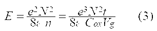
여기서 e는 전기소량, N은 채널 내의 단위면적당 평균결함밀도, ε는 반도체의 유전률, n은 단위면적당 채널에 포함되는 캐리어 수, Cox는 단위면적당 용량, Vg는 게이트 전압, t는 채널의 두께이다. 또한, 두께 30nm 이하의 반도체층이면, 채널의 두께는 반도체층의 두께와 동일하게 해도 상관없다. 선형 영역에서의 드레인 전류(Id)는 다음의 식 (4)로 표현할 수 있다.Where e is the amount of electricity, N is the average defect density per unit area in the channel, ε is the dielectric constant of the semiconductor, n is the number of carriers in the channel per unit area, C ox is the capacity per unit area, V g is the gate voltage, and t is the Thickness. The thickness of the channel may be the same as the thickness of the semiconductor layer as long as it is a semiconductor layer having a thickness of 30 nm or less. The drain current I d in the linear region can be expressed by the following equation (4).
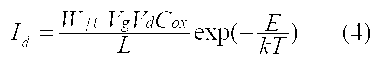
여기서, L은 채널길이, W는 채널 폭이며, 여기서는 L=W=10㎛이다. 또한 Vd는 드레인 전압이다. 상기 식 (4)의 양 변을 Vg로 나누고, 나아가 양 변의 대수를 취하면, 다음의 식 (5)가 된다.Where L is the channel length and W is the channel width, where L = W = 10 mu m. V d is a drain voltage. Dividing the both sides of the formula (4) in V g, Furthermore, by taking the logarithm both sides, is the following equation (5).

식 (5)의 우변은 Vg의 함수이다. 이 식으로부터 알 수 있듯이, 세로축을 ln(Id/Vg), 횡축을 1/Vg로 하는 직선의 기울기로부터 결함밀도(N)가 구해진다. 즉, 트랜지스터의 Id-Vg 특성으로부터 결함밀도를 평가할 수 있다. 산화물 반도체로서는 인듐(In), 주석(Sn), 아연(Zn)의 비율이 In:Sn:Zn=1:1:1인 것에서는 결함밀도(N)는 1×10¹²㎝-2 정도이다.The right side of equation (5) is a function of V g . As can be seen from this equation, the defect density N is obtained from the inclination of a straight line with the vertical axis as ln (I d / V g ) and the horizontal axis as 1 / Vg. That is, the defect density can be evaluated from the I d -V g characteristics of the transistor. As an oxide semiconductor, when the ratio of indium (In), tin (Sn), and zinc (Zn) is In: Sn: Zn = 1: 1: 1, the defect density (N) is about 1 × 10 12 cm -2 .
이와 같이 하여 구한 결함밀도 등을 기초로 식 (2) 및 식 (3)으로부터 μ0=120㎠/Vs가 도출된다. 결함이 있는 In-Sn-Zn 산화물에서 측정되는 이동도는 40㎠/Vs 정도이다. 그러나, 반도체 내부 및 반도체와 절연막과의 계면의 결함이 없는 산화물 반도체의 이동도(μ0)는 120㎠/Vs가 된다고 예상할 수 있다.Μ 0 = 120
단, 반도체 내부에 결함이 없어도, 채널과 게이트 절연물과의 계면에서의 산란에 의해 트랜지스터의 수송 특성은 영향을 받는다. 즉 게이트 절연물 계면으로부터 x만큼 떨어진 곳에서의 이동도(μ1)는 다음의 식 (6)으로 표현할 수 있다.However, even if there is no defect inside the semiconductor, the transport characteristics of the transistor are affected by scattering at the interface between the channel and the gate insulator. That is, the mobility μ 1 at a distance x from the gate insulator interface can be expressed by the following equation (6).
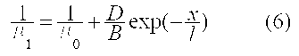
여기서, D는 게이트 방향의 전계, B, l는 상수이다. B 및 l는 실제의 측정 결과로부터 구할 수 있고, 상기 측정 결과로부터는 B=4.75×10⁷㎝/s, l=10nm(계면산란이 미치는 깊이)이다. D가 증가하면(즉, 게이트 전압이 높아지면) 식 (6)의 제2항이 증가되기 때문에, 이동도(μ1)는 저하되는 것을 알 수 있다.Where D is an electric field in the gate direction, and B and l are constants. B and 1 can be calculated | required from an actual measurement result, and it is B = 4.75 * 10 <7> cm / s and l = 10nm (depth which surface scattering has) from the said measurement result. It can be seen that since D increases (that is, when the gate voltage becomes high), the second term of equation (6) increases, so that the mobility μ 1 decreases.
반도체 내부의 결함이 없는 이상적인 산화물 반도체를 채널에 이용한 트랜지스터의 이동도(μ)를 계산한 결과를 도 13에 나타낸다. 또한, 계산에는 시놉시스사 제품 디바이스 시뮬레이션 소프트, Sentaurus Device를 사용하고, 산화물 반도체의 밴드갭, 전자친화력, 비유전률, 두께를 각각, 2.8 전자볼트, 4.7 전자볼트, 15, 15nm로 했다. 이들 값은 스퍼터링법에 의해 형성된 박막을 측정하여 얻어진 것이다.Fig. 13 shows the result of calculating the mobility [mu] of the transistor using the ideal oxide semiconductor without defects in the semiconductor as the channel. In addition, using the Synopsys device simulation software and Sentaurus Device, the band gap, electron affinity, relative dielectric constant, and thickness of the oxide semiconductor were set to 2.8 electron volts, 4.7 electron volts, 15 and 15 nm, respectively. These values are obtained by measuring the thin film formed by the sputtering method.
아울러, 게이트, 소스, 드레인의 일함수를 각각, 5.5 전자볼트, 4.6 전자볼트, 4.6 전자 볼트로 했다. 또한, 게이트 절연물의 두께는 100nm, 비유전률은 4.1로 했다. 채널 길이 및 채널 폭은 모두 10㎛, 드레인 전압(Vd)은 0.1V이다.In addition, the work functions of the gate, the source, and the drain were 5.5 electron volts, 4.6 electron volts, and 4.6 electron volts, respectively. In addition, the thickness of the gate insulator was 100 nm, and the dielectric constant was 4.1. Both the channel length and the channel width are 10 mu m, and the drain voltage V d is 0.1V.
도 13에 도시한 바와 같이, 게이트 전압 1V강에서 이동도 100㎠/Vs 이상의 피크를 갖지만, 게이트 전압이 더욱 높아지면 계면산란이 커지고, 이동도가 저하된다. 또한, 계면산란을 저감시키기 위해서는, 반도체층 표면을 원자 레벨로 평탄하게 하는 것(ALF: Atomic Layer Flatness)이 바람직하다.As shown in FIG. 13, although the peak of
이와 같은 이동도를 갖는 산화물 반도체를 이용하여 미세한 트랜지스터를 제작한 경우의 특성을 계산한 결과를 도 14 내지 도 16에 나타낸다. 또한, 계산에 이용한 트랜지스터의 단면 구조를 도 17에 도시한다. 도 17에 도시하는 트랜지스터는 산화물 반도체층에 n+의 도전형을 나타내는 제 2 영역(1103b) 및 제 2 영역(1103c)을 갖는다. 제 2 영역(1103b) 및 제 2 영역(1103c)의 저항률은 2×10⁻³Ω㎝로 한다.14 to 16 show the results of calculating the characteristics in the case of producing a fine transistor using the oxide semiconductor having such mobility. 17 shows the cross-sectional structure of the transistor used for the calculation. The transistor shown in FIG. 17 has a
도 17(A)에 도시하는 트랜지스터는 하지 절연막(1101)과, 하지 절연막(1101)에 메워 넣어지도록 형성된 산화 알루미늄으로 이루어지는 매립 절연물(1102) 상에 형성된다. 트랜지스터는 제 2 영역(1103b), 제 2 영역(1103c)과, 그들 사이에 마련되어 채널 형성 영역이 되는 진성의 제 1 영역(1103a)과, 게이트 전극(1105)을 갖는다. 게이트 전극(1105)의 폭(즉 채널 길이에 해당함.)을 33nm로 한다.The transistor shown in FIG. 17A is formed on a
게이트 전극(1105)과 제 1 영역(1103a)의 사이에는 게이트 절연막(1104)을 갖고, 또한, 게이트 전극(1105)의 양측면에는 사이드월 절연막(1106a) 및 사이드월 절연막(1106b), 게이트 전극(1105)의 상부에는 게이트 전극(1105)과 다른 배선과의 단락을 방지하기 위한 절연물(1107)을 갖는다. 사이드월 절연막의 폭은 5nm로 한다. 또한, 제 2 영역(1103b) 및 제 2 영역(1103c)에 접하여 소스 전극(1108a) 및 드레인 전극(1108b)을 갖는다. 또한, 이 트랜지스터에서의 채널 폭을 40nm로 한다.A
도 17(B)에 도시하는 트랜지스터는 하지 절연막(1101)과, 산화 알루미늄으로 이루어지는 매립 절연물(1102) 상에 형성되고, 제 2 영역(1103b), 제 2 영역(1103c)과, 그들 사이에 마련된 진성의 제 1 영역(1103a)과, 폭 33nm의 게이트 전극(1105)과 게이트 절연막(1104)과 사이드월 절연막(1106a) 및 사이드월 절연막(1106b)과 절연물(1107)과 소스 전극(1108a) 및 드레인 전극(1108b)을 갖는 점에서 도 17(A)에 도시하는 트랜지스터와 동일하다.The transistor shown in Fig. 17B is formed on a
도 17(A)에 도시하는 트랜지스터와 도 17(B)에 도시하는 트랜지스터의 차이점은, 사이드월 절연막(1106a) 및 사이드월 절연막(1106b) 아래의 반도체 영역의 도전형이다. 도 17(A)에 도시하는 트랜지스터에서는, 사이드월 절연막(1106a) 및 사이드월 절연막(1106b) 아래의 반도체 영역은 n+의 도전형을 나타내는 제 2 영역(1103b) 및 제 2 영역(1103c)이지만, 도 17(B)에 도시하는 트랜지스터에서는 진성의 제 1 영역(1103a)이다. 즉, 제 2 영역(1103b)(제 2 영역(1103c))과 게이트 전극(1105)이 Loff만큼 중첩되지 않는 영역이 형성되어 있다. 이 영역을 오프셋 영역이라고 하고, 그 폭(Loff)을 오프셋 길이라고 한다. 도면으로부터 분명하듯이, 오프셋 길이는 사이드월 절연막(1106a)(사이드월 절연막(1106b))의 폭과 동일하다.The difference between the transistor shown in Fig. 17A and the transistor shown in Fig. 17B is the conductivity type of the semiconductor region under the
그 외의 계산에 사용하는 파라미터는 상술한 바와 같다. 계산에는 시놉시스사 제품 디바이스 시뮬레이션 소프트, Sentaurus Device를 사용했다. 도 14는 도 17(A)에 도시되는 구조의 트랜지스터의 드레인 전류(Id)(실선) 및 이동도(μ)(점선)의 게이트 전압(Vg)(게이트와 소스의 전위차) 의존성을 나타낸다. 드레인 전류(Id)는 드레인 전압(드레인과 소스의 전위차)을 +1V로 하고, 이동도(μ)는 드레인 전압을 +0.1V로 하여 계산한 것이다.The parameters used for other calculations are as described above. The Synopsys device simulation software, Sentaurus Device, was used for the calculation. FIG. 14 shows the dependence of the drain current I d (solid line) and the mobility μ (dotted line) of the gate voltage V g (potential difference between the gate and the source) of the transistor shown in FIG. 17A. . The drain current I d calculates the drain voltage (potential difference between the drain and the source) at + 1V, and the mobility μ is calculated at the drain voltage of + 0.1V.
도 14(A)는 게이트 절연막의 두께를 15nm로 한 것이고, 도 14(B)는 10nm로 한 것이며, 도 14(C)는 5nm로 한 것이다. 게이트 절연막이 얇아질수록, 특히 오프 상태에서의 드레인 전류(Id)(오프 전류)가 현저하게 저하된다. 한편, 이동도(μ)의 피크값이나 온 상태에서의 드레인 전류(Id)(온 전류)에는 눈에 띄는 변화가 없다. 게이트 전압 1V 전후에서 드레인 전류는 메모리 소자 등에서 필요로 하는 10㎂를 초과하는 것이 나타났다.In Fig. 14A, the thickness of the gate insulating film is 15 nm, Fig. 14B is 10 nm, and Fig. 14C is 5 nm. As the gate insulating film becomes thinner, in particular, the drain current I d (off current) in the off state significantly decreases. On the other hand, there is no noticeable change in the peak value of the mobility μ or the drain current I d (on current) in the on state. Before and after the gate voltage of 1V, the drain current was found to exceed 10 mA required by the memory device and the like.
도 15는 도 17(B)에 도시되는 구조의 트랜지스터이며, 오프셋 길이(Loff) 를 5nm로 한 것의 드레인 전류(Id)(실선) 및 이동도(μ)(점선)의 게이트 전압(Vg) 의존성을 나타낸다. 드레인 전류(Id)는 드레인 전압을 +1V로 하고, 이동도(μ)는 드레인 전압을 +0.1V로 하여 계산한 것이다. 도 15(A)는 게이트 절연막의 두께를 15nm로 한 것이고, 도 15(B)는 10nm로 한 것이며, 도 15(C)는 5nm로 한 것이다.Fig. 15 is a transistor of the structure shown in Fig. 17B, and has a drain current I d (solid line) and a gate voltage V g of mobility μ (dotted line) having an offset length Loff of 5 nm. ) Indicates dependencies. The drain current I d is calculated by setting the drain voltage to + 1V and the mobility μ as the drain voltage to + 0.1V. 15 (A) shows the thickness of the gate insulating film at 15 nm, FIG. 15 (B) shows it as 10 nm, and FIG. 15 (C) shows 5 nm.
또한, 도 16은 도 17(B)에 도시되는 구조의 트랜지스터이며, 오프셋 길이(Loff)를 15nm로 한 것의 드레인 전류 (Id)(실선) 및 이동도(μ)(점선)의 게이트 전압 의존성을 나타낸다. 드레인 전류(Id)는 드레인 전압을 +1V로 하고, 이동도(μ)는 드레인 전압을 +0.1V로 하여 계산한 것이다. 도 16(A)는 게이트 절연막의 두께를 15nm로 한 것이고, 도 16(B)는 10nm로 한 것이며, 도 16(C)는 5nm로 한 것이다.Fig. 16 is a transistor having the structure shown in Fig. 17B, and has a gate voltage dependency of drain current I d (solid line) and mobility μ (dotted line) having an offset length Loff of 15 nm. Indicates. The drain current I d is calculated by setting the drain voltage to + 1V and the mobility μ as the drain voltage to + 0.1V. In Fig. 16A, the thickness of the gate insulating film is 15 nm, Fig. 16B is 10 nm, and Fig. 16C is 5 nm.
어느 것이나 모두 게이트 절연막이 얇아질수록 오프 전류가 현저하게 저하하는 한편, 이동도(μ)의 피크값이나 온 전류에는 눈에 띄는 변화가 없다.In both cases, the thinner the gate insulating film, the lower the off-state current is, but the peak value of the mobility μ and the on-state current are not noticeable.
또한, 이동도(μ)의 피크는 도 14에서는 80㎠/Vs 정도이지만, 도 15에서는 60㎠/Vs정도, 도 16에서는 40㎠/Vs로, 오프셋 길이(Loff)가 증가할수록 저하된다. 또한, 오프 전류도 동일한 경향을 갖는다. 한편, 온 전류는 오프셋 길이(Loff)의 증가에 따라 감소하지만, 오프 전류의 저하에 비해 훨씬 완만하다. 또한, 모두 게이트 전압 1V 전후에서, 드레인 전류는 메모리 소자 등에서 필요로 하는 10㎂를 초과하는 것으로 나타났다. 또한, 이와 같이 이동도가 높은 트랜지스터를 앞선 실시형태에서 나타낸 논리회로를 전환하기 위한 트랜지스터에 이용함으로써, 노드(N)에의 기입을 고속으로 수행할 수 있으므로, 동적 구성을 용이하게 수행할 수 있는 프로그래머블 로직 디바이스를 제공할 수 있다.The peak of the mobility μ is about 80
(실시형태 4)(Fourth Embodiment)
본 실시형태에서는, 앞선 실시형태에서 나타낸 산화물 반도체막을 갖는 트랜지스터에 대해서, 특히 In, Sn, Zn을 주성분으로 하는 산화물 반도체막을 갖는 트랜지스터에 대해서 설명한다.In the present embodiment, the transistor having the oxide semiconductor film shown in the above embodiment will be described, particularly the transistor having the oxide semiconductor film containing In, Sn, and Zn as a main component.
In, Sn, Zn을 주성분으로 하는 산화물 반도체를 채널 형성 영역으로 하는 트랜지스터는, 그 산화물 반도체를 형성할 때에 기판을 가열하여 성막함으로써, 또는 산화물 반도체막을 형성한 후에 열처리를 수행함으로써 양호한 특성을 얻을 수 있다. 또한, 주성분은 조성비로 5atomic% 이상 포함되는 원소를 말한다.A transistor having an oxide semiconductor whose main component is In, Sn or Zn as a channel forming region can be obtained by forming a film by heating the substrate when forming the oxide semiconductor or by performing a heat treatment after forming the oxide semiconductor film have. In addition, a main component means the element contained 5 atomic% or more by composition ratio.
In, Sn, Zn을 주성분으로 하는 산화물 반도체막의 성막 후에 기판을 의도적으로 가열함으로써, 트랜지스터의 전계 효과 이동도를 향상시키는 것이 가능해진다. 또한, 트랜지스터의 문턱값 전압을 플러스 시프트시켜, 노멀리 오프화시키는 것이 가능해진다. 이하, In, Sn, Zn을 주성분으로 하는 산화물 반도체막을 갖는 트랜지스터를 제작하여 각종 측정을 수행한 결과에 대해서 설명한다.By intentionally heating the substrate after the formation of the oxide semiconductor film containing In, Sn, and Zn as a main component, the field effect mobility of the transistor can be improved. In addition, it is possible to positively shift the threshold voltage of the transistor to turn it off normally. Hereinafter, the result of having performed the various measurements which produced the transistor which has the oxide semiconductor film which has In, Sn, Zn as a main component is demonstrated.
우선, 본 실시형태에서 각종 측정에 이용한 트랜지스터의 구조에 대해서 도 23을 이용하여 설명한다. 도 23(A)는 이 트랜지스터의 평면도이며, 도 23(B)는 도 23(A)의 일점쇄선 A-B에 대응하는 단면도이다.First, the structure of the transistor used for various measurements in the present embodiment will be described with reference to FIG. 23. Fig. 23A is a plan view of the transistor, and Fig. 23B is a sectional view corresponding to dashed-dotted line A-B in Fig. 23A.
도 23(B)에 도시하는 트랜지스터는, 기판(600)과, 기판(600) 상에 마련된 하지 절연막(602)과, 하지 절연막(602) 상에 마련된 산화물 반도체막(606)과, 산화물 반도체막(606)과 접하는 한 쌍의 전극(614)과, 산화물 반도체막(606) 및 한 쌍의 전극(614) 상에 마련된 게이트 절연막(608)과, 게이트 절연막(608)을 통해 산화물 반도체막(606)과 중첩되어 마련된 게이트 전극(610)과, 게이트 절연막(608) 및 게이트 전극(610)을 덮어 마련된 층간 절연막(616)과, 게이트 절연막(608) 및 층간 절연막(616)에 마련된 개구부를 통해 한 쌍의 전극(614)과 접속하는 배선(618)과, 층간 절연막(616) 및 배선(618)을 덮어 마련된 보호막(620)을 갖는다. 여기서, 한 쌍의 전극(614)은 이 트랜지스터의 소스 전극 및 드레인 전극으로서 기능한다.The transistor illustrated in FIG. 23B includes a
기판(600)으로서는 유리 기판을, 하지 절연막(602)으로서는 산화 실리콘막을, 산화물 반도체막(606)으로서는 In-Sn-Zn-O막을, 한 쌍의 전극(614)으로서는 텅스텐막을, 게이트 절연막(608)으로서는 산화 실리콘막을, 게이트 전극(610)으로서는 질화 탄탈막과 텅스텐막의 적층 구조를, 층간 절연막(616)으로서는 산화 질화 실리콘막과 폴리이미드막의 적층 구조를, 배선(618)으로서는 티타늄막, 알루미늄막, 티타늄막이 이 순서로 형성된 적층 구조를, 보호막(620)으로서는 폴리이미드막을, 각각 이용했다.A glass substrate as the
또한, 도 23(A)에 도시하는 구조의 트랜지스터에 있어서, 게이트 전극(610)과 한 쌍의 전극(614)의 중첩되는 폭을 Lov라고 부른다. 마찬가지로 산화물 반도체막(606)에 대한 한 쌍의 전극(614)이 중첩되지 않는 부분을 dW라고 부른다.In the transistor having the structure shown in Fig. 23A, the overlapping width of the
도 18(A)~도 18(C)는 도 23에 도시하는 트랜지스터에 있어서, 채널 길이(L)가 3㎛, 채널 폭(W)이 10㎛인 산화물 반도체막과, 두께 100nm의 게이트 절연막을 이용한 트랜지스터의 특성(드레인 전류(Id)(실선) 및 이동도(μ)(점선)의 게이트 전압 의존성)이다. 또한, Vd는 10V로 했다.18A to 18C show an oxide semiconductor film having a channel length L of 3 mu m and a channel width W of 10 mu m, and a gate insulating film having a thickness of 100 nm in the transistor shown in FIG. The characteristics of the transistor used (the gate voltage dependence of the drain current I d (solid line) and mobility μ (dashed line)). In addition, V d was made into 10V.
도 18(A)는 기판을 의도적으로 가열하지 않고 스퍼터링법으로 In, Sn, Zn을 주성분으로 하는 산화물 반도체막을 형성한 때의 트랜지스터 특성이다. 이때 전계 효과 이동도는 18.8㎠/Vs가 얻어지고 있다. 한편, 기판을 의도적으로 가열하여 In, Sn, Zn을 주성분으로 하는 산화물 반도체막을 형성하면 전계 효과 이동도를 향상시키는 것이 가능해진다. 도 18(B)는 기판을 200℃로 가열하여 In, Sn, Zn을 주성분으로 하는 산화물 반도체막을 형성한 때의 트랜지스터 특성을 나타내고 있는데, 전계 효과 이동도는 32.2㎠/Vs가 얻어지고 있다.Fig. 18A is a transistor characteristic when an oxide semiconductor film containing In, Sn, Zn as a main component is formed by sputtering without intentionally heating a substrate. At this time, the field effect mobility is 18.8
전계 효과 이동도는 In, Sn, Zn을 주성분으로 하는 산화물 반도체막을 형성한 후에 열처리를 함으로써 더욱 높일 수 있다. 도 18(C)는 In, Sn, Zn을 주성분으로 하는 산화물 반도체막을 200℃로 스퍼터링 성막한 후, 650℃로 열처리를 한 때의 트랜지스터 특성을 나타낸다. 이때 전계 효과 이동도는 34.5㎠/Vs가 얻어지고 있다.The field effect mobility can be further increased by heat treatment after forming an oxide semiconductor film containing In, Sn, and Zn as a main component. Fig. 18C shows transistor characteristics when an oxide semiconductor film containing In, Sn, and Zn as a main component is sputtered at 200 占 폚 and then heat treated at 650 占 폚. At this time, the field effect mobility is 34.5
기판을 의도적으로 가열함으로써 스퍼터링 성막 중의 수분이 산화물 반도체막 내로 들어가는 것을 저감시키는 효과를 기대할 수 있다. 또한, 성막 후에 열처리를 하는 것에 의해서도, 산화물 반도체막으로부터 수소나 수산기 또는 수분을 방출시켜 제거할 수 있고, 상기와 같이 전계 효과 이동도를 향상시킬 수 있다. 이와 같은 전계 효과 이동도의 향상은 탈수화?탈수소화 의한 불순물의 제거뿐만 아니라, 고밀도화에 의해 원자간 거리가 짧아지기 때문인 것으로도 추정된다. 또한, 산화물 반도체로부터 불순물을 제거하여 고순도화함으로써 결정화를 도모할 수 있다. 이와 같이 고순도화된 비단결정 산화물 반도체는 이상적으로는 100㎠/Vs를 초과하는 전계 효과 이동도를 실현하는 것도 가능해질 것으로 추정된다.By intentionally heating the substrate, an effect of reducing the moisture in the sputtering film into the oxide semiconductor film can be expected. Moreover, also by heat-processing after film-forming, hydrogen, a hydroxyl group, or water can be discharge | released and removed from an oxide semiconductor film, and the field effect mobility can be improved as mentioned above. Such improvement in the field effect mobility is presumed to be due not only to the removal of impurities due to dehydration and dehydrogenation, but also to the shortening of the interatomic distance due to high density. In addition, crystallization can be achieved by removing impurities from the oxide semiconductor and making it highly purified. It is estimated that such highly purified non-single crystal oxide semiconductors can realize field effect mobility ideally exceeding 100
In, Sn, Zn을 주성분으로 하는 산화물 반도체에 산소 이온을 주입하고, 열처리에 의해 그 산화물 반도체에 포함되는 수소나 수산기 또는 수분을 방출시켜, 그 열처리와 동시에 또는 그 후의 열처리에 의해 산화물 반도체를 결정화시킬 수도 있다. 이러한 결정화 또는 재결정화의 처리에 의해 결정성이 좋은 비단결정 산화물 반도체를 얻을 수 있다.Oxygen ions are implanted into an oxide semiconductor containing In, Sn, and Zn as main components, and hydrogen, hydroxyl or moisture contained in the oxide semiconductor are released by heat treatment, and the oxide semiconductor is crystallized by heat treatment simultaneously with or after the heat treatment. You can also By such crystallization or recrystallization, a non-single crystal oxide semiconductor having good crystallinity can be obtained.
기판을 의도적으로 가열하여 성막하는 것 및 성막 후에 열처리하는 것의 효과는 전계 효과 이동도의 향상뿐만 아니라, 트랜지스터의 노멀리 오프화를 도모하는 것에도 기여하고 있다. 기판을 의도적으로 가열하지 않고 형성된 In, Sn, Zn을 주성분으로 하는 산화물 반도체막을 채널 형성 영역으로 한 트랜지스터는 문턱값 전압이 마이너스 시프트해 버리는 경향이 있다. 그러나, 기판을 의도적으로 가열하여 형성된 산화물 반도체막을 이용한 경우, 이 문턱값 전압의 마이너스 시프트화는 해소된다. 즉, 문턱값 전압은 트랜지스터가 노멀리 오프가 되는 방향으로 움직이고, 이러한 경향은 도 18(A)와 도 18(B)의 대비로부터도 확인할 수 있다.The effects of intentionally heating the substrate to form a film and performing a heat treatment after the film formation contribute not only to the improvement of the field effect mobility but also to the normalization of the transistor. Transistors having an oxide semiconductor film mainly composed of In, Sn, Zn formed as a channel forming region without intentionally heating a substrate tend to have negative threshold voltage shifts. However, when the oxide semiconductor film formed by intentionally heating the substrate is used, the negative shift of this threshold voltage is eliminated. That is, the threshold voltage moves in the direction in which the transistor is normally off, and this tendency can also be confirmed from the contrast of Figs. 18A and 18B.
또한, 문턱값 전압은 In, Sn 및 Zn의 비율을 변경하는 것에 의해서도 제어할 수 있으며, 조성비로서 In:Sn:Zn=2:1:3으로 함으로써 트랜지스터의 노멀리 오프화를 기대할 수 있다. 또한, 타겟의 조성비를 In:Sn:Zn=2:1:3으로 함으로써 결정성이 높은 산화물 반도체막을 얻을 수 있다.The threshold voltage can also be controlled by changing the ratios of In, Sn, and Zn. As the composition ratio, In: Sn: Zn = 2: 1: 3, the transistor can be normally turned off. In addition, an oxide semiconductor film having high crystallinity can be obtained by setting the composition ratio of the target to In: Sn: Zn = 2: 1: 3.
의도적인 기판 가열 온도 또는 열처리 온도는 150℃ 이상, 바람직하게는 200℃ 이상, 보다 바람직하게는 400℃ 이상이며, 보다 고온으로 성막하거나 또는 열처리함으로써 트랜지스터의 노멀리 오프화를 도모하는 것이 가능해진다.The intentional substrate heating temperature or heat treatment temperature is 150 ° C. or higher, preferably 200 ° C. or higher, more preferably 400 ° C. or higher, and the transistor can be normally off by forming a film at a higher temperature or by heat treatment.
열처리는 산소 분위기중에서 수행할 수 있으나, 우선 질소 또는 불활성 가스, 또는 감압하에서 열처리를 수행한 후에 산소를 포함하는 분위기중에서 열처리를 수행할 수도 있다. 처음에 탈수화?탈수소화를 수행한 후에 산소를 산화물 반도체에 가함으로써, 열처리의 효과를 보다 높일 수 있다. 또한, 나중에 산소를 가하려면, 산소 이온을 전계로 가속하여 산화물 반도체막에 주입하는 방법을 적용할 수도 있다.The heat treatment may be performed in an oxygen atmosphere, but first, the heat treatment may be performed under nitrogen or an inert gas or under reduced pressure, and then heat treatment may be performed in an atmosphere containing oxygen. After the dehydration and dehydrogenation are first performed, the effect of heat treatment can be further enhanced by adding oxygen to the oxide semiconductor. In order to add oxygen later, a method of accelerating oxygen ions into an electric field and implanting it into the oxide semiconductor film may be applied.
산화물 반도체 내 및 적층되는 막과의 계면에는 산소 결손에 의한 결함이 생성되기 쉬우나, 이러한 열처리에 의해 산화물 반도체 내에 산소를 과잉으로 포함시킴으로써, 정상적으로 생성되는 산소 결손을 과잉인 산소에 의해 보상하는 것이 가능해진다. 과잉 산소는 주로 격자 사이에 존재하는 산소이며, 그 산소 농도는 1×10¹⁶㎝-3 이상 2×10²⁰㎝-3 이하로 하면 결정에 왜곡 등을 주지 않으면서 산화물 반도체 내에 포함시킬 수 있다.Defects due to oxygen deficiency tend to be generated at the interface between the oxide semiconductor and the stacked film, but by incorporating oxygen in the oxide semiconductor excessively by such heat treatment, it is possible to compensate the oxygen deficiency normally generated by excess oxygen. Become. The excess oxygen is mainly oxygen present between the lattice, and when the oxygen concentration is set to 1 × 10 16 cm −3 or more and 2 × 10 20 cm −3 or less, it can be included in the oxide semiconductor without giving distortion or the like to the crystal.
또한, 열처리에 의해 산화물 반도체에 결정이 적어도 일부에 포함되도록 함으로써, 보다 안정된 산화물 반도체막을 얻을 수 있다. 예를 들어, 조성비 In:Sn:Zn=1:1:1의 타겟을 사용하여, 기판을 의도적으로 가열하지 않고 스퍼터링 성막한 산화물 반도체막은 X선 회절(XRD: X-Ray Diffraction)로 할로 패턴이 관측된다. 이 성막된 산화물 반도체막을 열처리함으로써 결정화시킬 수 있다. 열처리 온도는 임의이지만, 예를 들어 650℃의 열처리를 수행함으로써, X선 회절에 의해 명확한 회절 피크를 관측할 수 있다.In addition, a more stable oxide semiconductor film can be obtained by allowing crystals to be included in at least a part of the oxide semiconductor by heat treatment. For example, an oxide semiconductor film sputtered without intentionally heating a substrate using a target having a composition ratio In: Sn: Zn = 1: 1: 1 has a halo pattern formed by X-ray diffraction (XRD). Is observed. It can crystallize by heat-processing this formed oxide semiconductor film. Although the heat treatment temperature is arbitrary, it is possible to observe a clear diffraction peak by X-ray diffraction, for example, by performing a heat treatment at 650 ° C.
실제로 In-Sn-Zn-O막의 XRD 분석을 수행했다. XRD 분석에는 Bruker AXS사 제품 X선 회절장치 D8 ADVANCE를 사용하고 Out-of-Plane법으로 측정했다.In fact, XRD analysis of the In—Sn—Zn—O film was performed. XRD analysis was performed using an X-ray diffractometer D8 ADVANCE manufactured by Bruker AXS, and measured out-of-plane method.
XRD 분석을 수행한 시료로서 시료 A 및 시료 B를 준비했다. 이하에 시료 A 및 시료 B의 제작 방법을 설명한다.Sample A and Sample B were prepared as samples subjected to XRD analysis. Hereinafter, the production methods of the sample A and the sample B will be described.
탈수소화 처리가 끝난 석영기판 상에 In-Sn-Zn-O막을 100nm의 두께로 성막했다.An In—Sn—Zn—O film was formed to a thickness of 100 nm on the dehydrogenation quartz substrate.
In-Sn-Zn-O막은 스퍼터링 장치를 사용하여 산소 분위기에서 전력을 100W(DC)로 하여 성막했다. 타겟은 In:Sn:Zn=1:1:1[원자수비]의 In-Sn-Zn-O 타겟을 사용했다. 또한, 성막 시의 기판 가열 온도는 200℃로 했다. 이와 같이 하여 제작한 시료를 시료 A로 했다.The In-Sn-Zn-O film was formed by using a sputtering apparatus at 100 W (DC) electric power in an oxygen atmosphere. As the target, an In-Sn-Zn-O target having an In: Sn: Zn = 1: 1: 1 [atomic ratio] was used. In addition, the board | substrate heating temperature at the time of film-forming was 200 degreeC. The sample thus produced was referred to as Sample A.
이어서, 시료 A와 동일한 방법으로 제작한 시료에 대해 가열 처리를 650℃의 온도로 수행했다. 가열 처리는 처음에 질소 분위기에서 1시간의 가열 처리를 수행하고, 온도를 내리지 않고 산소 분위기에서 추가로 1시간의 가열 처리를 수행하고 있다. 이와 같이 하여 제작한 시료를 시료 B로 했다.Next, the heat processing was performed at the temperature of 650 degreeC with respect to the sample produced by the method similar to sample A. The heat treatment is first performed in a nitrogen atmosphere for 1 hour, and is further performed in an oxygen atmosphere for 1 hour without lowering the temperature. Thus, the sample produced was made into sample B.
도 19에 시료 A 및 시료 B의 XRD 스펙트럼을 도시한다. 시료 A에서는 결정에서 유래하는 피크가 관측되지 않았으나, 시료 B에서는 2θ가 35deg 근방 및 37deg~38deg에 결정에서 유래하는 피크가 관측되었다.19 shows XRD spectra of Sample A and Sample B. FIG. In sample A, the peak derived from the crystal was not observed, but in sample B, the peak derived from the crystal was observed in the vicinity of 35 deg and 37 deg to 38 deg in 2θ.
이와 같이, In, Sn, Zn을 주성분으로 하는 산화물 반도체는 성막 시에 의도적으로 가열하는 것 및/또는 성막 후에 열처리함으로써 트랜지스터의 특성을 향상시킬 수 있다.As described above, the oxide semiconductor containing In, Sn, and Zn as a main component can be improved by intentionally heating during film formation and / or by heat treatment after film formation.
이 기판 가열이나 열처리는 산화물 반도체에 있어서 악성의 불순물인 수소나 수산기를 막내에 포함시키지 않도록 하는 것, 또는 막내로부터 제거하는 작용이 있다. 즉, 산화물 반도체 내에서 도너 불순물이 되는 수소를 제거함으로써 고순도화를 도모할 수 있고, 그에 따라 트랜지스터의 노멀리 오프화를 도모할 수 있고, 산화물 반도체가 고순도화됨으로써 오프 전류를 1aA/㎛ 이하로 할 수 있다. 여기서, 상기 오프 전류값의 단위는 채널 폭 1㎛당 전류값을 나타낸다.This substrate heating or heat treatment serves to prevent hydrogen or hydroxyl groups, which are malignant impurities in the oxide semiconductor, from being contained in the film or to remove them from the film. That is, high purity can be achieved by removing hydrogen, which is a donor impurity, in the oxide semiconductor, whereby normalization of the transistor can be achieved, and high purity of the oxide semiconductor allows the off current to be 1aA / µm or less. can do. Here, the unit of the off current value represents a current value per 1 μm of the channel width.
도 20에 트랜지스터의 오프 전류와 측정시의 기판온도(절대온도)의 역수와의 관계를 나타낸다. 여기서는, 간단화를 위해 측정시의 기판온도의 역수에 1000을 곱한 수치(1000/T)를 횡축으로 하고 있다.20 shows the relationship between the off current of the transistor and the inverse of the substrate temperature (absolute temperature) at the time of measurement. Here, for simplicity, the horizontal axis represents a numerical value (1000 / T) obtained by multiplying the inverse of the substrate temperature at the time of measurement by 1000.
구체적으로는 도 20에 도시한 바와 같이, 기판온도가 125℃인 경우에는 0.1aA/㎛(1×10-19A/㎛) 이하, 85℃인 경우에는 10zA/㎛(1×10-20A/㎛) 이하였다. 전류값의 대수가 온도의 역수에 비례하므로, 실온(27℃)인 경우에는 0.1zA/㎛(1×10-22A/㎛) 이하로 예상된다. 따라서, 오프 전류를 125℃에서 1aA/㎛(1×10-18A/㎛) 이하로, 85℃에서 100zA/㎛(1×10-19A/㎛) 이하로, 실온에서 1zA/㎛(1×10-21A/㎛) 이하로 할 수 있다.Specifically, as shown in FIG. 20, when the substrate temperature is 125 ° C., 0.1 aA / μm (1 × 10 −19 A / μm) or less, and when it is 85 ° C., 10 zA / μm (1 × 10 −20 A) / Mu m) or less. Since the logarithm of the current value is proportional to the inverse of the temperature, it is expected to be 0.1zA / µm (1 × 10 -22 A / µm) or less at room temperature (27 ° C). Thus, the off current is 1 aA / μm (1 × 10 -18 A / μm) or less at 125 ° C, 100 zA / μm (1 × 10 -19 A / μm) or less at 85 ° C, and 1 zA / μm (1 at room temperature). × 10 -21 A / µm) or less.
무엇보다, 산화물 반도체막의 성막 시에 수소나 수분이 막내에 혼입되지 않도록, 처리실 외부로부터의 리크나 처리실 내의 내벽으로부터의 탈가스를 충분히 억제하고, 스퍼터링 가스의 고순도화를 도모하는 것이 바람직하다. 예를 들어, 스퍼터링 가스는 수분이 막내에 포함되지 않도록 노점 -70℃ 이하인 가스를 사용하는 것이 바람직하다. 또한, 타겟 그 자체에 수소나 수분 등의 불순물이 포함되어 있지 않도록, 고순도화된 타겟을 사용하는 것이 바람직하다. In, Sn, Zn을 주성분으로 하는 산화물 반도체는 열처리에 의해 막내의 수분을 제거할 수 있으나, In, Ga, Zn을 주성분으로 하는 산화물 반도체와 비교하여 수분의 방출 온도가 높기 때문에, 바람직하게는 처음부터 수분이 포함되지 않는 막을 형성해 두는 것이 바람직하다.Above all, it is preferable to sufficiently suppress the leakage from the outside of the processing chamber and the degassing from the inner wall of the processing chamber so as not to mix hydrogen and moisture into the film during film formation of the oxide semiconductor film, and to achieve high purity of the sputtering gas. For example, as the sputtering gas, it is preferable to use a gas having a dew point of −70 ° C. or lower so that moisture is not contained in the film. In addition, it is preferable to use a highly purified target so that the target itself does not contain impurities such as hydrogen and water. The oxide semiconductor containing In, Sn, Zn as a main component can remove moisture in the film by heat treatment. However, since the release temperature of water is higher than that of the oxide semiconductor containing In, Ga, Zn as a main component, It is desirable to form a film containing no moisture therefrom.
또한, 산화물 반도체막 성막 후에 650℃의 가열 처리를 수행한 시료의 트랜지스터에 있어서, 기판온도와 전기적 특성의 관계에 대해서 평가했다.Moreover, in the transistor of the sample which heat-processed at 650 degreeC after oxide semiconductor film film-forming, the relationship between board | substrate temperature and electrical property was evaluated.
측정에 이용한 트랜지스터는 채널 길이(L)가 3㎛, 채널 폭(W)이 10㎛, Lov가 편측 3㎛(합계 6㎛), dW가 0㎛이다. 또한, Vd는 10V로 했다. 또한, 기판온도는 -40℃, -25℃, 25℃, 75℃, 125℃ 및 150℃로 수행했다. 여기서, 트랜지스터에 있어서, 게이트 전극과 한 쌍의 전극과의 중첩되는 폭을 Lov라고 부르고, 산화물 반도체막에 대한 한 쌍의 전극이 중첩되지 않는 부분을 dW라고 부른다.The transistor used for the measurement has a channel length L of 3 mu m, a channel width W of 10 mu m, a Lov on one side of 3 mu m (total 6 mu m), and a dW of 0 mu m. In addition, V d was made into 10V. In addition, substrate temperature was performed at -40 degreeC, -25 degreeC, 25 degreeC, 75 degreeC, 125 degreeC, and 150 degreeC. Here, in the transistor, the overlapping width of the gate electrode with the pair of electrodes is called Lov, and the portion where the pair of electrodes with respect to the oxide semiconductor film does not overlap is called dW.
도 21에 Id(실선) 및 전계 효과 이동도(점선)의 Vg 의존성을 나타낸다. 또한, 도 22(A)에 기판온도와 문턱값 전압의 관계를 나타내고, 도 22(B)에 기판온도와 전계 효과 이동도의 관계를 나타낸다.21 shows V g dependence of I d (solid line) and field effect mobility (dashed line). 22A shows the relationship between the substrate temperature and the threshold voltage, and FIG. 22B shows the relationship between the substrate temperature and the field effect mobility.
도 22(A)로부터 기판온도가 높을수록 문턱값 전압은 낮아지는 것을 알 수 있다. 또한, 그 범위는 -40℃~150℃에서 1.09V~-0.23V였다.It can be seen from FIG. 22A that the higher the substrate temperature is, the lower the threshold voltage is. Moreover, the range was 1.09V --0.23V at -40 degreeC-150 degreeC.
또한, 도 22(B)로부터 기판온도가 높을수록 전계 효과 이동도가 낮아지는 것을 알 수 있다. 또한, 그 범위는 -40℃~150℃에서 36㎠/Vs~32㎠/Vs였다. 따라서, 상술한 온도범위에서 전기적 특성의 변동이 작은 것을 알 수 있다.In addition, it can be seen from FIG. 22B that the higher the substrate temperature, the lower the field effect mobility. Moreover, the range was 36 cm <2> / Vs-32 cm <2> / Vs at -40 degreeC-150 degreeC. Therefore, it can be seen that the variation of the electrical characteristics is small in the above-described temperature range.
상기와 같은 In, Sn, Zn을 주성분으로 하는 산화물 반도체를 채널 형성 영역으로 하는 트랜지스터에 의하면, 오프 전류를 1aA/㎛ 이하로 유지하면서, 전계 효과 이동도를 30㎠/Vs 이상, 바람직하게는 40㎠/Vs 이상, 보다 바람직하게는 60㎠/Vs 이상으로 하여, LSI에서 요구되는 온 전류의 값을 충족시킬 수 있다. 예를 들어, L/W=33nm/40nm인 FET에서, 게이트 전압 2.7V, 드레인 전압 1.0V인 때 12㎂ 이상의 온 전류를 흐르게 할 수 있다.According to the transistor having an oxide semiconductor mainly composed of In, Sn, and Zn as a channel forming region, the field effect mobility is 30
이와 같이 오프 전류가 낮은 트랜지스터를 앞선 실시형태에서 나타낸 논리회로를 전환하기 위한 트랜지스터에 이용함으로써, 전원 전위의 공급이 차단되었을 때에도 노드(N)의 전하 유지 상태를 유지하는 것이 가능해진다. 이에 따라, 전원 투입 후의 노드(N)에의 데이터의 기입을 생략하는 것이 가능해지므로, 논리 블록의 기동 시간을 짧게 할 수 있다. 따라서, 노멀리 오프의 구동 방법을 이용하여, 저소비전력화를 도모할 수 있는 프로그래머블 로직 디바이스를 제공할 수 있다.By using the transistor having a low off current as the transistor for switching the logic circuit shown in the above embodiment, the charge holding state of the node N can be maintained even when the supply of the power supply potential is interrupted. This makes it possible to omit writing of data to the node N after the power is turned on, so that the startup time of the logical block can be shortened. Therefore, a programmable logic device capable of lowering power consumption can be provided by using a normally off driving method.
또한, 이와 같이 이동도가 높은 트랜지스터를 앞선 실시형태에서 나타낸 논리회로를 전환하기 위한 트랜지스터에 이용함으로써, 노드(N)에의 데이터의 기입을 고속으로 수행할 수 있으므로, 동적 구성을 용이하게 수행할 수 있는 프로그래머블 로직 디바이스를 제공할 수 있다.In addition, by using the transistor having high mobility in the transistor for switching the logic circuit shown in the foregoing embodiment, writing of data to the node N can be performed at high speed, so that a dynamic configuration can be easily performed. Programmable logic devices can be provided.
또한, 이와 같은 특성이라면, Si 반도체로 만들어지는 집적회로 내에 산화물 반도체로 형성되는 트랜지스터를 혼재해도, 동작 속도를 희생하지 않는 프로그래머블 로직 디바이스를 제공할 수 있다.Moreover, with such characteristics, a programmable logic device can be provided that does not sacrifice operating speed even when a transistor formed of an oxide semiconductor is mixed in an integrated circuit made of a Si semiconductor.
(실시형태 5)(Embodiment 5)
본 발명의 일 양태에 따른 논리회로를 이용함으로써 소비전력이 낮은 전자기기를 제공하는 것이 가능하다. 특히 전력 공급을 상시 받기 어려운 휴대용 전자기기의 경우, 본 발명의 일 양태에 따른 소비전력이 낮은 반도체 장치를 그 구성요소에 추가함으로써, 연속 사용시간이 길어진다고 하는 장점이 얻어진다.It is possible to provide an electronic device with low power consumption by using a logic circuit according to one aspect of the present invention. In particular, in the case of a portable electronic device which is hard to receive power supply at all times, the advantage that the continuous use time is long is obtained by adding the low power consumption semiconductor device according to one aspect of the present invention to its components.
본 발명의 일 양태에 있어서의 논리회로를 이용한 반도체 장치는 표시장치, 퍼스널 컴퓨터, 기록매체를 구비한 화상재생장치(대표적으로는 DVD: Digital Versatile Disc 등의 기록매체를 재생하고, 그 화상을 표시할 수 있는 디스플레이를 갖는 장치)에 이용할 수 있다. 그 외에, 본 발명의 일 양태에 따른 반도체 장치를 이용할 수 있는 전자기기로서, 휴대전화, 휴대형을 포함하는 게임기, 휴대정보단말, 전자 서적, 비디오 카메라, 디지털 카메라, 고글형 디스플레이(헤드 마운트 디스플레이), 내비게이션 시스템, 음향재생장치(카오디오, 디지털 오디오 플레이어 등), 복사기, 팩시밀리, 프린터, 프린터 복합기, 현금자동입출금기(ATM), 자동 판매기 등을 들 수 있다.In a semiconductor device using a logic circuit in one aspect of the present invention, an image reproducing apparatus (typically a DVD: Digital Versatile Disc such as a DVD) is provided with a display device, a personal computer, and a recording medium, and the image is displayed. Device having a display capable of doing so). In addition, as an electronic device that can use the semiconductor device according to an aspect of the present invention, a mobile phone, a game machine including a portable type, a portable information terminal, an electronic book, a video camera, a digital camera, a goggle type display (head mounted display) , Navigation systems, sound reproducing apparatuses (car audio, digital audio players, etc.), copiers, fax machines, printers, multifunction printers, ATMs, and vending machines.
본 발명의 일 양태에 있어서의 논리회로를 이용한 반도체 장치를 휴대전화, 스마트 폰, 전자 서적 등의 휴대용 전자기기에 응용한 경우에 대해서 설명한다.The case where the semiconductor device using the logic circuit in one aspect of the present invention is applied to a portable electronic device such as a cellular phone, a smart phone, or an electronic book will be described.
도 8은 휴대용 전자기기의 블럭도이다. 도 8에 도시하는 휴대용 전자기기는 RF 회로(421), 아날로그 베이스밴드 회로(422), 디지털 베이스밴드 회로(423), 배터리(424), 전원회로(425), 어플리케이션 프로세서(426), 플래시메모리(430), 디스플레이 콘트롤러(431), 메모리 회로(432), 디스플레이(433), 터치 센서(439), 음성회로(437), 키보드(438) 등으로 구성되어 있다. 디스플레이(433)는 표시부(434), 소스 드라이버(435), 게이트 드라이버(436)에 의해 구성되어 있다. 어플리케이션 프로세서(426)는 CPU(427), DSP(428), 인터페이스(429)를 갖고 있다. 예를 들어, CPU(427), 디지털 베이스밴드 회로(423), 메모리 회로(432), DSP(428), 인터페이스(429), 디스플레이 콘트롤러(431), 음성회로(437) 중 어느 하나 또는 모두에 상기 실시형태에서 나타낸 프로그래머블 로직 디바이스를 채용함으로써, 소비전력을 저감시킬 수 있다.8 is a block diagram of a portable electronic device. The portable electronic device shown in FIG. 8 includes an
도 9는 전자 서적의 블럭도이다. 전자 서적은 배터리(451), 전원회로(452), 마이크로 프로세서(453), 플래시메모리(454), 음성회로(455), 키보드(456), 메모리 회로(457), 터치 패널(458), 디스플레이(459), 디스플레이 콘트롤러(460)에 의해 구성된다. 마이크로 프로세서(453)는 CPU(461), DSP(462), 인터페이스(463)를 갖고 있다. 예를 들어, CPU(461), 음성회로(455), 메모리 회로(457), 디스플레이 콘트롤러(460), DSP(462), 인터페이스(463) 중 어느 하나 또는 모두에 상기 실시형태에서 나타낸 프로그래머블 로직 디바이스를 채용함으로써, 소비전력을 저감시키는 것이 가능해진다.9 is a block diagram of an electronic book. The electronic book includes a
본 실시형태는 상기 실시형태와 적절히 조합하여 실시하는 것이 가능하다.This embodiment can be implemented in appropriate combination with the above embodiment.
이상, 본 실시형태에 나타내는 구성, 방법 등은 다른 실시형태에 나타내는 구성, 방법 등과 적절히 조합하여 이용할 수 있다.As mentioned above, the structure, method, etc. which are shown in this embodiment can be used in combination with the structure, method, etc. which are shown in another embodiment.
101 : 트랜지스터 102 : 트랜지스터
103 : 트랜지스터 104 : 트랜지스터
105 : 트랜지스터 106 : 트랜지스터
107 : 트랜지스터 108 : 트랜지스터
109 : 트랜지스터 110 : 트랜지스터
111 : 트랜지스터 201 : 반도체 기판
203 : 소자 분리 영역 205 : p웰 영역
215 : 절연막 217 : 절연막
221 : 절연막 225 : 절연막
227 : 산화물 반도체막 229 : 산화물 반도체막
231 : 절연막 233 : 게이트 전극
235 : 산화물 반도체막 237 : 사이드월 절연막
239 : 게이트 절연막 243 : 절연막
245 : 절연막 249 : 배선
250 : 배선 421 : RF 회로
422 : 아날로그 베이스밴드 회로 423 : 디지털 베이스밴드 회로
424 : 배터리 425 : 전원회로
426 : 어플리케이션 프로세서 427 : CPU
428 : DSP 429 : 인터페이스
430 : 플래시메모리 431 : 디스플레이 콘트롤러
432 : 메모리 회로 433 : 디스플레이
434 : 표시부 435 : 소스 드라이버
436 : 게이트 드라이버 437 : 음성회로
438 : 키보드 439 : 터치 센서
451 :배터리 452 : 전원회로
453 : 마이크로 프로세서 454 : 플래시메모리
455 : 음성회로 456 : 키보드
457 : 메모리 회로 458 : 터치 패널
459 : 디스플레이 460 : 디스플레이 콘트롤러
461 : CPU 462 : DSP
463 : 인터페이스 600 : 기판
602 : 하지 절연막 606 : 산화물 반도체막
608 : 게이트 절연막 610 : 게이트 전극
614 : 전극 616 : 층간 절연막
618 : 배선 620 : 보호막
1101 : 하지 절연막 1102 : 절연물
1104 : 게이트 절연막 1105 : 게이트 전극
1107 : 절연물 207a : 게이트 절연막
207b : 게이트 절연막 209a : 게이트 전극
209b : 게이트 전극 211a : 불순물 영역
211b : 불순물 영역 213a : 불순물 영역
213b : 불순물 영역 219a : 콘택 플러그
219b : 콘택 플러그 219c : 콘택 플러그
219d : 콘택 플러그 223a : 배선
223b : 배선 223c : 배선
235a : 영역 235b : 영역
235c : 영역 241a : 전극
241b : 전극 1103a : 영역
1103b : 영역 1103c : 영역
1106a : 사이드월 절연막 1106b : 사이드월 절연막
1108a : 소스 전극 1108b : 드레인 전극101: transistor 102: transistor
103: transistor 104: transistor
105: transistor 106: transistor
107: transistor 108: transistor
109: transistor 110: transistor
111
203: device isolation region 205: p well region
215: insulating film 217: insulating film
221
227
231
235
239: gate insulating film 243: insulating film
245: insulating film 249: wiring
250: wiring 421: RF circuit
422: analog baseband circuit 423: digital baseband circuit
424
426: Application processor 427: CPU
428: DSP 429: interface
430
432: memory circuit 433: display
434
436: gate driver 437: voice circuit
438: keyboard 439: touch sensor
451: battery 452: power circuit
453: microprocessor 454: flash memory
455: voice circuit 456: keyboard
457: memory circuit 458: touch panel
459: Display 460: Display Controller
461: CPU 462: DSP
463: interface 600: substrate
602: base insulating film 606: oxide semiconductor film
608: gate insulating film 610: gate electrode
614
618: wiring 620: protective film
1101: base insulating film 1102: insulator
1104: gate insulating film 1105: gate electrode
1107: Insulator 207a: Gate insulating film
207b:
209b:
211b:
213b:
219b:
219d: Contact plug 223a: Wiring
223b:
235a:
235c:
241b: electrode 1103a: area
1103b:
1106a: sidewall insulating
1108a:
Claims (15)
제 1 트랜지스터 내지 제 4 트랜지스터,
제 5 트랜지스터 내지 제 8 트랜지스터,
게이트가 서로 전기적으로 접속하는 제 9 트랜지스터 및 제 10 트랜지스터, 및
소스와 드레인 중 하나가 제 9 트랜지스터 및 제 10 트랜지스터의 게이트와 전기적으로 접속하는 제 11 트랜지스터를 갖고,
제 1 트랜지스터의 소스와 드레인 중 하나가 제 5 트랜지스터의 소스와 드레인 중 하나에 전기적으로 접속되며,
제 4 트랜지스터의 소스와 드레인 중 하나가 제 8 트랜지스터의 소스와 드레인 중 하나에 전기적으로 접속되며,
제 1 트랜지스터의 게이트, 제 3 트랜지스터의 게이트, 및 제 8 트랜지스터의 게이트는 서로 전기적으로 접속되고,
제 2 트랜지스터의 게이트, 제 4 트랜지스터의 게이트, 및 제 5 트랜지스터의 게이트는 서로 전기적으로 접속되며,
제 6 트랜지스터의 게이트, 제 7 트랜지스터의 게이트, 제 9 트랜지스터의 게이트, 및 제 10 트랜지스터의 게이트는, 제 11 트랜지스터의 소스와 드레인 중 하나에 전기적으로 접속되어 노드가 형성되고,
제 9 트랜지스터의 소스와 드레인 중 하나는, 제 1 트랜지스터의 소스와 드레인 중 나머지 하나와 제 2 트랜지스터의 소스와 드레인 중 하나에 전기적으로 접속되며,
제 9 트랜지스터의 소스와 드레인 중 나머지 하나는, 제 5 트랜지스터의 소스와 드레인 중 나머지 하나와 제 6 트랜지스터의 소스와 드레인 중 하나에 전기적으로 접속되고,
제 10 트랜지스터의 소스와 드레인 중 하나는, 제 3 트랜지스터의 소스와 드레인 중 하나와 제 4 트랜지스터의 소스와 드레인 중 나머지 하나에 전기적으로 접속되며,
제 10 트랜지스터의 소스와 드레인 중 나머지 하나는, 제 7 트랜지스터의 소스와 드레인 중 하나와 제 8 트랜지스터의 소스와 드레인 중 나머지 하나에 전기적으로 접속되고,
제 2 트랜지스터의 소스와 드레인 중 나머지 하나, 제 3 트랜지스터의 소스와 드레인 중 나머지 하나, 제 6 트랜지스터의 소스와 드레인 중 나머지 하나, 및 제 7 트랜지스터의 소스와 드레인 중 나머지 하나는 서로 전기적으로 접속되며,
제 11 트랜지스터는 산화물 반도체를 포함하는, 논리회로.
As a logic circuit,
First to fourth transistors,
Fifth to eighth transistors,
A ninth transistor and a tenth transistor whose gates are electrically connected to each other, and
One of the source and the drain has an eleventh transistor electrically connected to the gates of the ninth and tenth transistors,
One of the source and the drain of the first transistor is electrically connected to one of the source and the drain of the fifth transistor,
One of the source and the drain of the fourth transistor is electrically connected to one of the source and the drain of the eighth transistor,
The gate of the first transistor, the gate of the third transistor, and the gate of the eighth transistor are electrically connected to each other,
The gate of the second transistor, the gate of the fourth transistor, and the gate of the fifth transistor are electrically connected to each other,
The gate of the sixth transistor, the gate of the seventh transistor, the gate of the ninth transistor, and the gate of the tenth transistor are electrically connected to one of a source and a drain of the eleventh transistor, and a node is formed.
One of the source and the drain of the ninth transistor is electrically connected to the other of the source and the drain of the first transistor and one of the source and the drain of the second transistor,
The other of the source and the drain of the ninth transistor is electrically connected to the other of the source and the drain of the fifth transistor and one of the source and the drain of the sixth transistor,
One of the source and the drain of the tenth transistor is electrically connected to one of the source and the drain of the third transistor and the other of the source and the drain of the fourth transistor,
The other of the source and the drain of the tenth transistor is electrically connected to one of the source and the drain of the seventh transistor and the other of the source and the drain of the eighth transistor,
The other of the source and the drain of the second transistor, the other of the source and the drain of the third transistor, the other of the source and the drain of the sixth transistor, and the other of the source and the drain of the seventh transistor are electrically connected to each other. ,
And the eleventh transistor comprises an oxide semiconductor.
상기 노드와 전기적으로 접속하는 용량 소자를 더 포함하는, 논리회로.
The method of claim 1,
And a capacitive element in electrical connection with said node.
상기 노드에서의 전하 유지 상태를 전환함으로써, 부정 논리합(NOR) 회로 또는 부정 논리곱(NAND) 회로로 전환할 수 있는, 논리회로.
The method of claim 1,
A logic circuit capable of switching to a negative OR circuit or a NAND circuit by switching the charge holding state at the node.
상기 제 1 트랜지스터, 제 2 트랜지스터, 제 5 트랜지스터, 제 6 트랜지스터, 및 제 9 트랜지스터는 p채널 트랜지스터이며,
제 3 트랜지스터, 제 4 트랜지스터, 제 7 트랜지스터, 제 8 트랜지스터, 제 10 트랜지스터, 및 제 11 트랜지스터는 n채널 트랜지스터인, 논리회로.
The method of claim 1,
The first transistor, the second transistor, the fifth transistor, the sixth transistor, and the ninth transistor are p-channel transistors,
And the third transistor, the fourth transistor, the seventh transistor, the eighth transistor, the tenth transistor, and the eleventh transistor are n-channel transistors.
상기 산화물 반도체는 In, Ga, Sn, 및 Zn으로부터 선택된 적어도 한 원소를 포함하는, 논리회로.
The method of claim 1,
And the oxide semiconductor comprises at least one element selected from In, Ga, Sn, and Zn.
제 1 트랜지스터 내지 제 4 트랜지스터,
제 5 트랜지스터 내지 제 8 트랜지스터,
게이트가 서로 전기적으로 접속하는 제 9 트랜지스터 및 제 10 트랜지스터, 및
소스와 드레인 중 하나가 제 9 트랜지스터 및 제 10 트랜지스터의 게이트와 전기적으로 접속하는 제 11 트랜지스터를 갖고,
제 1 트랜지스터의 소스와 드레인 중 하나가 제 5 트랜지스터의 소스와 드레인 중 하나에 전기적으로 접속되며,
제 4 트랜지스터의 소스와 드레인 중 하나가 제 8 트랜지스터의 소스와 드레인 중 하나에 전기적으로 접속되며,
제 1 트랜지스터의 게이트, 제 3 트랜지스터의 게이트, 및 제 8 트랜지스터의 게이트는 서로 전기적으로 접속되고,
제 2 트랜지스터의 게이트, 제 4 트랜지스터의 게이트, 및 제 5 트랜지스터의 게이트는 서로 전기적으로 접속되며,
제 6 트랜지스터의 게이트, 제 7 트랜지스터의 게이트, 제 9 트랜지스터의 게이트, 및 제 10 트랜지스터의 게이트가, 제 11 트랜지스터의 소스와 드레인 중 하나에 전기적으로 접속되어 노드가 형성되고,
제 9 트랜지스터의 소스와 드레인 중 하나는, 제 1 트랜지스터의 소스와 드레인 중 나머지 하나와 제 2 트랜지스터의 소스와 드레인 중 하나에 전기적으로 접속되며,
제 9 트랜지스터의 소스와 드레인 중 나머지 하나는, 제 5 트랜지스터의 소스와 드레인 중 나머지 하나와 제 6 트랜지스터의 소스와 드레인 중 하나에 전기적으로 접속되고,
제 10 트랜지스터의 소스와 드레인 중 하나는, 제 3 트랜지스터의 소스와 드레인 중 하나와 제 4 트랜지스터의 소스와 드레인 중 나머지 하나에 전기적으로 접속되며,
제 10 트랜지스터의 소스와 드레인 중 나머지 하나는, 제 7 트랜지스터의 소스와 드레인 중 하나와 제 8 트랜지스터의 소스와 드레인 중 나머지 하나에 전기적으로 접속되고,
제 2 트랜지스터의 소스와 드레인 중 나머지 하나, 제 3 트랜지스터의 소스와 드레인 중 나머지 하나, 제 6 트랜지스터의 소스와 드레인 중 나머지 하나, 및 제 7 트랜지스터의 소스와 드레인 중 나머지 하나는 서로 전기적으로 접속되며,
제 11 트랜지스터는 산화물 반도체를 포함하고,
제 11 트랜지스터는 제 1 트랜지스터 내지 제 10 트랜지스터 위에 적층되는, 논리회로.
As a logic circuit,
First to fourth transistors,
Fifth to eighth transistors,
A ninth transistor and a tenth transistor whose gates are electrically connected to each other, and
One of the source and the drain has an eleventh transistor electrically connected to the gates of the ninth and tenth transistors,
One of the source and the drain of the first transistor is electrically connected to one of the source and the drain of the fifth transistor,
One of the source and the drain of the fourth transistor is electrically connected to one of the source and the drain of the eighth transistor,
The gate of the first transistor, the gate of the third transistor, and the gate of the eighth transistor are electrically connected to each other,
The gate of the second transistor, the gate of the fourth transistor, and the gate of the fifth transistor are electrically connected to each other,
The gate of the sixth transistor, the gate of the seventh transistor, the gate of the ninth transistor, and the gate of the tenth transistor are electrically connected to one of the source and the drain of the eleventh transistor to form a node,
One of the source and the drain of the ninth transistor is electrically connected to the other of the source and the drain of the first transistor and one of the source and the drain of the second transistor,
The other of the source and the drain of the ninth transistor is electrically connected to the other of the source and the drain of the fifth transistor and one of the source and the drain of the sixth transistor,
One of the source and the drain of the tenth transistor is electrically connected to one of the source and the drain of the third transistor and the other of the source and the drain of the fourth transistor,
The other of the source and the drain of the tenth transistor is electrically connected to one of the source and the drain of the seventh transistor and the other of the source and the drain of the eighth transistor,
The other of the source and the drain of the second transistor, the other of the source and the drain of the third transistor, the other of the source and the drain of the sixth transistor, and the other of the source and the drain of the seventh transistor are electrically connected to each other. ,
The eleventh transistor comprises an oxide semiconductor,
An eleventh transistor is stacked over the first to tenth transistors.
상기 노드와 전기적으로 접속하는 용량 소자를 더 포함하는, 논리회로.
The method according to claim 6,
And a capacitive element in electrical connection with said node.
상기 노드에서의 전하 유지 상태를 전환함으로써, 부정 논리합(NOR) 회로 또는 부정 논리곱(NAND) 회로로 전환할 수 있는, 논리회로.
The method according to claim 6,
A logic circuit capable of switching to a negative OR circuit or a NAND circuit by switching the charge holding state at the node.
상기 제 1 트랜지스터, 제 2 트랜지스터, 제 5 트랜지스터, 제 6 트랜지스터 및 제 9 트랜지스터는 p채널 트랜지스터이며,
제 3 트랜지스터, 제 4 트랜지스터, 제 7 트랜지스터, 제 8 트랜지스터, 제 10 트랜지스터 및 제 11 트랜지스터는 n채널 트랜지스터인, 논리회로.
The method according to claim 6,
The first transistor, the second transistor, the fifth transistor, the sixth transistor, and the ninth transistor are p-channel transistors,
And the third transistor, the fourth transistor, the seventh transistor, the eighth transistor, the tenth transistor, and the eleventh transistor are n-channel transistors.
상기 산화물 반도체는 In, Ga, Sn, 및 Zn으로부터 선택된 적어도 한 원소를 포함하는, 논리회로.
The method according to claim 6,
And the oxide semiconductor comprises at least one element selected from In, Ga, Sn, and Zn.
제 1 트랜지스터 내지 제 4 트랜지스터,
제 5 트랜지스터 내지 제 8 트랜지스터,
게이트가 서로 전기적으로 접속하는 제 9 트랜지스터 및 제 10 트랜지스터, 및
소스 또는 드레인의 한쪽이 제 9 트랜지스터 및 제 10 트랜지스터의 게이트와 전기적으로 접속하는 제 11 트랜지스터를 갖고,
제 1 트랜지스터의 소스와 드레인 중 하나와, 제 5 트랜지스터의 소스와 드레인 중 하나는, 고전위 전원선에 전기적으로 접속되며,
제 4 트랜지스터의 소스와 드레인 중 하나와, 제 8 트랜지스터의 소스와 드레인 중 하나는, 접지 또는 저전위 전원선에 전기적으로 접속되고,
제 1 트랜지스터, 제 3 트랜지스터 및 제 8 트랜지스터의 게이트는 제 1 신호선에 전기적으로 접속되며,
제 2 트랜지스터, 제 4 트랜지스터 및 제 5 트랜지스터의 게이트는 제 2 신호선에 전기적으로 접속되고,
제 6 트랜지스터, 제 7 트랜지스터, 제 9 트랜지스터 및 제 10 트랜지스터의 게이트는 제 11 트랜지스터의 소스와 드레인 중 하나와 전기적으로 접속하여 노드를 형성하며,
제 11 트랜지스터의 소스와 드레인 중 나머지 하나는 제 3 신호선과 전기적으로 접속하고,
제 11 트랜지스터의 게이트는 제 5 신호선과 전기적으로 접속하며,
제 9 트랜지스터의 소스와 드레인 중 하나는 제 1 트랜지스터의 소스와 드레인 중 나머지 하나 및 제 2 트랜지스터의 소스와 드레인 중 하나와 전기적으로 접속하고,
제 9 트랜지스터의 소스와 드레인 중 나머지 하나는 제 5 트랜지스터의 소스 와 드레인 중 나머지 하나 및 제 6 트랜지스터의 소스와 드레인 중 하나와 전기적으로 접속하며,
제 10 트랜지스터의 소스와 드레인 중 하나는 제 3 트랜지스터의 소스와 드레인 중 하나 및 제 4 트랜지스터의 소스 또는 드레인 중 나머지 하나와 전기적으로 접속하고,
제 10 트랜지스터의 소스와 드레인 중 나머지 하나는 제 7 트랜지스터의 소스와 드레인 중 하나 및 제 8 트랜지스터의 소스와 드레인 중 나머지 하나와 전기적으로 접속하며,
제 2 트랜지스터의 소스와 드레인 중 나머지 하나, 제 3 트랜지스터의 소스 와 드레인 중 나머지 하나, 제 6 트랜지스터의 소스와 드레인 중 나머지 하나 및 제 7 트랜지스터의 소스와 드레인 중 나머지 하나는 제 4 신호선과 전기적으로 접속하고,
제 11 트랜지스터는 산화물 반도체를 포함하는, 논리회로.
As a logic circuit,
First to fourth transistors,
Fifth to eighth transistors,
A ninth transistor and a tenth transistor whose gates are electrically connected to each other, and
One of the source or the drain has an eleventh transistor electrically connected to the gates of the ninth transistor and the tenth transistor,
One of the source and the drain of the first transistor and one of the source and the drain of the fifth transistor are electrically connected to a high potential power line,
One of the source and the drain of the fourth transistor and one of the source and the drain of the eighth transistor are electrically connected to a ground or low potential power line,
Gates of the first transistor, the third transistor, and the eighth transistor are electrically connected to the first signal line,
Gates of the second transistor, the fourth transistor, and the fifth transistor are electrically connected to the second signal line,
Gates of the sixth, seventh, ninth, and tenth transistors are electrically connected to one of a source and a drain of the eleventh transistor to form a node,
The other of the source and the drain of the eleventh transistor is electrically connected to the third signal line,
A gate of the eleventh transistor is electrically connected to the fifth signal line,
One of the source and the drain of the ninth transistor is electrically connected to the other of the source and the drain of the first transistor and one of the source and the drain of the second transistor,
The other of the source and the drain of the ninth transistor is electrically connected to the other of the source and the drain of the fifth transistor and one of the source and the drain of the sixth transistor,
One of the source and the drain of the tenth transistor is electrically connected to one of the source and the drain of the third transistor and the other of the source or the drain of the fourth transistor,
The other of the source and the drain of the tenth transistor is electrically connected to one of the source and the drain of the seventh transistor and the other of the source and the drain of the eighth transistor,
The other of the source and the drain of the second transistor, the other of the source and the drain of the third transistor, the other of the source and the drain of the sixth transistor and the other of the source and the drain of the seventh transistor are electrically connected to the fourth signal line. Connected,
And the eleventh transistor comprises an oxide semiconductor.
상기 노드와 전기적으로 접속하는 용량 소자를 더 포함하는, 논리회로.
The method of claim 11,
And a capacitive element in electrical connection with said node.
상기 노드에서의 전하 유지 상태를 전환함으로써, 부정 논리합(NOR) 회로 또는 부정 논리곱(NAND) 회로로 전환할 수 있는, 논리회로.
The method of claim 11,
A logic circuit capable of switching to a negative OR circuit or a NAND circuit by switching the charge holding state at the node.
상기 제 1 트랜지스터, 제 2 트랜지스터, 제 5 트랜지스터, 제 6 트랜지스터 및 제 9 트랜지스터는 p채널 트랜지스터이며,
제 3 트랜지스터, 제 4 트랜지스터, 제 7 트랜지스터, 제 8 트랜지스터, 제 10 트랜지스터 및 제 11 트랜지스터는 n채널 트랜지스터인, 논리회로.
The method of claim 11,
The first transistor, the second transistor, the fifth transistor, the sixth transistor, and the ninth transistor are p-channel transistors,
And the third transistor, the fourth transistor, the seventh transistor, the eighth transistor, the tenth transistor, and the eleventh transistor are n-channel transistors.
상기 산화물 반도체는 In, Ga, Sn, 및 Zn으로부터 선택된 적어도 한 원소를 포함하는, 논리회로.
The method of claim 11,
And the oxide semiconductor comprises at least one element selected from In, Ga, Sn, and Zn.
Applications Claiming Priority (2)
| Application Number | Priority Date | Filing Date | Title |
|---|---|---|---|
| JPJP-P-2011-112804 | 2011-05-19 | ||
| JP2011112804 | 2011-05-19 |
Publications (2)
| Publication Number | Publication Date |
|---|---|
| KR20120129782A true KR20120129782A (en) | 2012-11-28 |
| KR101854869B1 KR101854869B1 (en) | 2018-05-04 |
Family
ID=47174484
Family Applications (1)
| Application Number | Title | Priority Date | Filing Date |
|---|---|---|---|
| KR1020120051532A Expired - Fee Related KR101854869B1 (en) | 2011-05-19 | 2012-05-15 | Logic circuit |
Country Status (3)
| Country | Link |
|---|---|
| US (2) | US8779799B2 (en) |
| JP (3) | JP5914153B2 (en) |
| KR (1) | KR101854869B1 (en) |
Families Citing this family (24)
| Publication number | Priority date | Publication date | Assignee | Title |
|---|---|---|---|---|
| US8779799B2 (en) * | 2011-05-19 | 2014-07-15 | Semiconductor Energy Laboratory Co., Ltd. | Logic circuit |
| US9467047B2 (en) * | 2011-05-31 | 2016-10-11 | Semiconductor Energy Laboratory Co., Ltd. | DC-DC converter, power source circuit, and semiconductor device |
| US8995218B2 (en) | 2012-03-07 | 2015-03-31 | Semiconductor Energy Laboratory Co., Ltd. | Semiconductor device |
| WO2013164958A1 (en) | 2012-05-02 | 2013-11-07 | Semiconductor Energy Laboratory Co., Ltd. | Programmable logic device |
| WO2013176199A1 (en) | 2012-05-25 | 2013-11-28 | Semiconductor Energy Laboratory Co., Ltd. | Programmable logic device and semiconductor device |
| JP6377317B2 (en) | 2012-05-30 | 2018-08-22 | 株式会社半導体エネルギー研究所 | Programmable logic device |
| JP2014022507A (en) * | 2012-07-17 | 2014-02-03 | Toshiba Corp | Non-volatile programmable switch |
| TWI591966B (en) | 2012-10-17 | 2017-07-11 | 半導體能源研究所股份有限公司 | Programmable logic device and method for driving programmable logic device |
| KR102102589B1 (en) | 2012-10-17 | 2020-04-22 | 가부시키가이샤 한도오따이 에네루기 켄큐쇼 | Programmable logic device |
| WO2014077295A1 (en) | 2012-11-15 | 2014-05-22 | Semiconductor Energy Laboratory Co., Ltd. | Liquid crystal display device |
| JP6254834B2 (en) | 2012-12-06 | 2017-12-27 | 株式会社半導体エネルギー研究所 | Semiconductor device |
| US8952723B2 (en) * | 2013-02-13 | 2015-02-10 | Semiconductor Energy Laboratory Co., Ltd. | Programmable logic device and semiconductor device |
| US9704886B2 (en) | 2013-05-16 | 2017-07-11 | Semiconductor Energy Laboratory Co., Ltd. | Signal processing device |
| JP6473626B2 (en) | 2014-02-06 | 2019-02-20 | 株式会社半導体エネルギー研究所 | Semiconductor device |
| JP6625328B2 (en) | 2014-03-06 | 2019-12-25 | 株式会社半導体エネルギー研究所 | Method for driving semiconductor device |
| JP6541376B2 (en) | 2014-03-13 | 2019-07-10 | 株式会社半導体エネルギー研究所 | Method of operating programmable logic device |
| TWI643457B (en) | 2014-04-25 | 2018-12-01 | 日商半導體能源研究所股份有限公司 | Semiconductor device |
| TW201614626A (en) | 2014-09-05 | 2016-04-16 | Semiconductor Energy Lab | Display device and electronic device |
| KR20170091139A (en) | 2014-12-01 | 2017-08-08 | 가부시키가이샤 한도오따이 에네루기 켄큐쇼 | Display device, display module having said display device, and electronic device having said display device or said display module |
| KR102643895B1 (en) | 2015-10-30 | 2024-03-05 | 가부시키가이샤 한도오따이 에네루기 켄큐쇼 | Semiconductor device, electronic component, and electronic device |
| WO2018033834A1 (en) | 2016-08-19 | 2018-02-22 | Semiconductor Energy Laboratory Co., Ltd. | Method for controlling power supply in semiconductor device |
| US11189658B2 (en) | 2017-11-22 | 2021-11-30 | Taiwan Semiconductor Manufacturing Co., Ltd. | Magnetic random access memory and manufacturing method thereof |
| US11770117B2 (en) | 2021-12-07 | 2023-09-26 | Nanya Technology Corporation | Data receiving circuit |
| US11728794B2 (en) * | 2021-12-03 | 2023-08-15 | Nanya Technology Corporation | Data receiving circuit |
Family Cites Families (166)
| Publication number | Priority date | Publication date | Assignee | Title |
|---|---|---|---|---|
| US4870302A (en) | 1984-03-12 | 1989-09-26 | Xilinx, Inc. | Configurable electrical circuit having configurable logic elements and configurable interconnects |
| JPS60198861A (en) | 1984-03-23 | 1985-10-08 | Fujitsu Ltd | Thin film transistor |
| JPH0244256B2 (en) | 1987-01-28 | 1990-10-03 | Kagaku Gijutsucho Mukizaishitsu Kenkyushocho | INGAZN2O5DESHIMESARERUROTSUHOSHOKEINOSOJOKOZOOJUSURUKAGOBUTSUOYOBISONOSEIZOHO |
| JPH0244260B2 (en) | 1987-02-24 | 1990-10-03 | Kagaku Gijutsucho Mukizaishitsu Kenkyushocho | INGAZN5O8DESHIMESARERUROTSUHOSHOKEINOSOJOKOZOOJUSURUKAGOBUTSUOYOBISONOSEIZOHO |
| JPH0244258B2 (en) | 1987-02-24 | 1990-10-03 | Kagaku Gijutsucho Mukizaishitsu Kenkyushocho | INGAZN3O6DESHIMESARERUROTSUHOSHOKEINOSOJOKOZOOJUSURUKAGOBUTSUOYOBISONOSEIZOHO |
| JPS63210023A (en) | 1987-02-24 | 1988-08-31 | Natl Inst For Res In Inorg Mater | Compound having a hexagonal layered structure represented by InGaZn↓4O↓7 and its manufacturing method |
| JPH0244262B2 (en) | 1987-02-27 | 1990-10-03 | Kagaku Gijutsucho Mukizaishitsu Kenkyushocho | INGAZN6O9DESHIMESARERUROTSUHOSHOKEINOSOJOKOZOOJUSURUKAGOBUTSUOYOBISONOSEIZOHO |
| JPH0244263B2 (en) | 1987-04-22 | 1990-10-03 | Kagaku Gijutsucho Mukizaishitsu Kenkyushocho | INGAZN7O10DESHIMESARERUROTSUHOSHOKEINOSOJOKOZOOJUSURUKAGOBUTSUOYOBISONOSEIZOHO |
| JP2682009B2 (en) * | 1988-05-23 | 1997-11-26 | 日本電気株式会社 | Selection circuit |
| JP2749185B2 (en) * | 1990-07-11 | 1998-05-13 | シャープ株式会社 | Composite logic circuit |
| JP2990773B2 (en) * | 1990-09-18 | 1999-12-13 | 日本電気株式会社 | Selection circuit |
| JPH05251705A (en) | 1992-03-04 | 1993-09-28 | Fuji Xerox Co Ltd | Thin-film transistor |
| JPH05259882A (en) * | 1992-03-10 | 1993-10-08 | Fujitsu Ltd | Level conversion circuit device |
| US5250855A (en) * | 1992-03-20 | 1993-10-05 | Vlsi Technology, Inc. | Fast logic circuits |
| US5164612A (en) | 1992-04-16 | 1992-11-17 | Kaplinsky Cecil H | Programmable CMOS flip-flop emptying multiplexers |
| JP3059589B2 (en) * | 1992-09-29 | 2000-07-04 | 富士通株式会社 | Semiconductor integrated circuit device |
| KR960003373B1 (en) | 1992-09-29 | 1996-03-09 | 후지쓰 가부시키가이샤 | Programmable Logic Circuit |
| US5381058A (en) | 1993-05-21 | 1995-01-10 | At&T Corp. | FPGA having PFU with programmable output driver inputs |
| WO1995000921A1 (en) | 1993-06-25 | 1995-01-05 | Fraunhofer-Gesellschaft zur Förderung der angewandten Forschung e.V. | Configurable analog and digital array |
| JP3430231B2 (en) * | 1994-09-21 | 2003-07-28 | 富士通株式会社 | Logic cell and semiconductor integrated circuit using the same |
| JP3479375B2 (en) | 1995-03-27 | 2003-12-15 | 科学技術振興事業団 | Metal oxide semiconductor device in which a pn junction is formed with a thin film transistor made of a metal oxide semiconductor such as cuprous oxide, and methods for manufacturing the same |
| US5545579A (en) | 1995-04-04 | 1996-08-13 | Taiwan Semiconductor Manufacturing Company | Method of fabricating a sub-quarter micrometer channel field effect transistor having elevated source/drain areas and lightly doped drains |
| US5568067A (en) * | 1995-06-30 | 1996-10-22 | Cyrix Corporation | Configurable XNOR/XOR element |
| DE69635107D1 (en) | 1995-08-03 | 2005-09-29 | Koninkl Philips Electronics Nv | SEMICONDUCTOR ARRANGEMENT WITH A TRANSPARENT CIRCUIT ELEMENT |
| JP3625598B2 (en) | 1995-12-30 | 2005-03-02 | 三星電子株式会社 | Manufacturing method of liquid crystal display device |
| US5796128A (en) | 1996-07-25 | 1998-08-18 | Translogic Technology, Inc. | Gate array with fully wired multiplexer circuits |
| JP4103968B2 (en) | 1996-09-18 | 2008-06-18 | 株式会社半導体エネルギー研究所 | Insulated gate type semiconductor device |
| JP3106998B2 (en) | 1997-04-11 | 2000-11-06 | 日本電気株式会社 | Programmable logic LSI with additional memory |
| US6057707A (en) | 1997-06-20 | 2000-05-02 | Altera Corporation | Programmable logic device incorporating a memory efficient interconnection device |
| JP3185727B2 (en) | 1997-10-15 | 2001-07-11 | 日本電気株式会社 | Programmable function block |
| JP4170454B2 (en) | 1998-07-24 | 2008-10-22 | Hoya株式会社 | Article having transparent conductive oxide thin film and method for producing the same |
| JP3488105B2 (en) * | 1998-11-09 | 2004-01-19 | 日本電信電話株式会社 | Logic circuit and logic circuit device for preventing operation analysis |
| JP2000150861A (en) | 1998-11-16 | 2000-05-30 | Tdk Corp | Oxide thin film |
| JP3276930B2 (en) | 1998-11-17 | 2002-04-22 | 科学技術振興事業団 | Transistor and semiconductor device |
| US6118300A (en) | 1998-11-24 | 2000-09-12 | Xilinx, Inc. | Method for implementing large multiplexers with FPGA lookup tables |
| TW460731B (en) | 1999-09-03 | 2001-10-21 | Ind Tech Res Inst | Electrode structure and production method of wide viewing angle LCD |
| KR100516693B1 (en) | 2003-04-02 | 2005-09-22 | 주식회사 하이닉스반도체 | Non-volatile programmable logic circuit |
| KR100317331B1 (en) | 1999-11-11 | 2001-12-24 | 박종섭 | Nonvolatile ferroelectric memory device and method for manufacturing the same |
| JP2001168198A (en) * | 1999-12-09 | 2001-06-22 | Sony Corp | Memory embedded semiconductor integrated circuit and design method thereof |
| US6288593B1 (en) * | 2000-01-04 | 2001-09-11 | Translogic Technology, Inc. | Digital electronic circuit for use in implementing digital logic functions |
| US6384628B1 (en) | 2000-03-31 | 2002-05-07 | Cypress Semiconductor Corp. | Multiple voltage supply programmable logic device |
| JP4089858B2 (en) | 2000-09-01 | 2008-05-28 | 国立大学法人東北大学 | Semiconductor device |
| KR20020038482A (en) | 2000-11-15 | 2002-05-23 | 모리시타 요이찌 | Thin film transistor array, method for producing the same, and display panel using the same |
| JP3997731B2 (en) | 2001-03-19 | 2007-10-24 | 富士ゼロックス株式会社 | Method for forming a crystalline semiconductor thin film on a substrate |
| JP2002289859A (en) | 2001-03-23 | 2002-10-04 | Minolta Co Ltd | Thin film transistor |
| JP2003115754A (en) * | 2001-06-06 | 2003-04-18 | Matsushita Electric Ind Co Ltd | Nonvolatile selector and integrated circuit device |
| JP4090716B2 (en) | 2001-09-10 | 2008-05-28 | 雅司 川崎 | Thin film transistor and matrix display device |
| JP3925839B2 (en) | 2001-09-10 | 2007-06-06 | シャープ株式会社 | Semiconductor memory device and test method thereof |
| DE10152888A1 (en) | 2001-10-26 | 2003-05-15 | Infineon Technologies Ag | Integrated analog multiplexer used in analog signal processing, has switches that selectively connect multiplexer inputs to inverting input terminal of operational amplifier |
| WO2003040441A1 (en) | 2001-11-05 | 2003-05-15 | Japan Science And Technology Agency | Natural superlattice homologous single crystal thin film, method for preparation thereof, and device using said single crystal thin film |
| JP4164562B2 (en) | 2002-09-11 | 2008-10-15 | 独立行政法人科学技術振興機構 | Transparent thin film field effect transistor using homologous thin film as active layer |
| EP1324495B1 (en) | 2001-12-28 | 2011-03-30 | Fujitsu Semiconductor Limited | Programmable logic device with ferrroelectric configuration memories |
| JP4083486B2 (en) | 2002-02-21 | 2008-04-30 | 独立行政法人科学技術振興機構 | Method for producing LnCuO (S, Se, Te) single crystal thin film |
| CN1445821A (en) | 2002-03-15 | 2003-10-01 | 三洋电机株式会社 | Forming method of ZnO film and ZnO semiconductor layer, semiconductor element and manufacturing method thereof |
| JP3933591B2 (en) | 2002-03-26 | 2007-06-20 | 淳二 城戸 | Organic electroluminescent device |
| US7339187B2 (en) | 2002-05-21 | 2008-03-04 | State Of Oregon Acting By And Through The Oregon State Board Of Higher Education On Behalf Of Oregon State University | Transistor structures |
| US6856542B2 (en) * | 2002-06-04 | 2005-02-15 | Stmicroelectronics, Inc. | Programmable logic device circuit and method of fabricating same |
| JP2004022625A (en) | 2002-06-13 | 2004-01-22 | Murata Mfg Co Ltd | Semiconductor device and method of manufacturing the semiconductor device |
| US7105868B2 (en) | 2002-06-24 | 2006-09-12 | Cermet, Inc. | High-electron mobility transistor with zinc oxide |
| US7327169B2 (en) * | 2002-09-25 | 2008-02-05 | Semiconductor Energy Laboratory Co., Ltd. | Clocked inverter, NAND, NOR and shift register |
| US7067843B2 (en) | 2002-10-11 | 2006-06-27 | E. I. Du Pont De Nemours And Company | Transparent oxide semiconductor thin film transistors |
| JP4166105B2 (en) | 2003-03-06 | 2008-10-15 | シャープ株式会社 | Semiconductor device and manufacturing method thereof |
| JP2004273732A (en) | 2003-03-07 | 2004-09-30 | Sharp Corp | Active matrix substrate and manufacturing method thereof |
| JP4108633B2 (en) | 2003-06-20 | 2008-06-25 | シャープ株式会社 | THIN FILM TRANSISTOR, MANUFACTURING METHOD THEREOF, AND ELECTRONIC DEVICE |
| US7262463B2 (en) | 2003-07-25 | 2007-08-28 | Hewlett-Packard Development Company, L.P. | Transistor including a deposited channel region having a doped portion |
| US6856173B1 (en) | 2003-09-05 | 2005-02-15 | Freescale Semiconductor, Inc. | Multiplexing of digital signals at multiple supply voltages in an integrated circuit |
| DE10354501B4 (en) | 2003-11-21 | 2007-07-05 | Infineon Technologies Ag | Logic circuit arrangement |
| US7030651B2 (en) | 2003-12-04 | 2006-04-18 | Viciciv Technology | Programmable structured arrays |
| US7282782B2 (en) | 2004-03-12 | 2007-10-16 | Hewlett-Packard Development Company, L.P. | Combined binary oxide semiconductor device |
| CN102867855B (en) | 2004-03-12 | 2015-07-15 | 独立行政法人科学技术振兴机构 | Amorphous oxide and thin film transistor |
| US7297977B2 (en) | 2004-03-12 | 2007-11-20 | Hewlett-Packard Development Company, L.P. | Semiconductor device |
| US7145174B2 (en) | 2004-03-12 | 2006-12-05 | Hewlett-Packard Development Company, Lp. | Semiconductor device |
| US7242614B2 (en) * | 2004-03-30 | 2007-07-10 | Impinj, Inc. | Rewriteable electronic fuses |
| KR20050099259A (en) * | 2004-04-09 | 2005-10-13 | 삼성전자주식회사 | High speed flipflops and complex gates using thereof |
| US7348827B2 (en) | 2004-05-19 | 2008-03-25 | Altera Corporation | Apparatus and methods for adjusting performance of programmable logic devices |
| US7129745B2 (en) | 2004-05-19 | 2006-10-31 | Altera Corporation | Apparatus and methods for adjusting performance of integrated circuits |
| US7400167B2 (en) | 2005-08-16 | 2008-07-15 | Altera Corporation | Apparatus and methods for optimizing the performance of programmable logic devices |
| US7211825B2 (en) | 2004-06-14 | 2007-05-01 | Yi-Chi Shih | Indium oxide-based thin film transistors and circuits |
| JP2006100760A (en) | 2004-09-02 | 2006-04-13 | Casio Comput Co Ltd | Thin film transistor and manufacturing method thereof |
| US7285501B2 (en) | 2004-09-17 | 2007-10-23 | Hewlett-Packard Development Company, L.P. | Method of forming a solution processed device |
| US7298084B2 (en) | 2004-11-02 | 2007-11-20 | 3M Innovative Properties Company | Methods and displays utilizing integrated zinc oxide row and column drivers in conjunction with organic light emitting diodes |
| US7791072B2 (en) | 2004-11-10 | 2010-09-07 | Canon Kabushiki Kaisha | Display |
| RU2358355C2 (en) | 2004-11-10 | 2009-06-10 | Кэнон Кабусики Кайся | Field transistor |
| US7453065B2 (en) | 2004-11-10 | 2008-11-18 | Canon Kabushiki Kaisha | Sensor and image pickup device |
| CA2585190A1 (en) | 2004-11-10 | 2006-05-18 | Canon Kabushiki Kaisha | Amorphous oxide and field effect transistor |
| US7829444B2 (en) | 2004-11-10 | 2010-11-09 | Canon Kabushiki Kaisha | Field effect transistor manufacturing method |
| US7863611B2 (en) | 2004-11-10 | 2011-01-04 | Canon Kabushiki Kaisha | Integrated circuits utilizing amorphous oxides |
| CN101057333B (en) | 2004-11-10 | 2011-11-16 | 佳能株式会社 | Light emitting device |
| US7579224B2 (en) | 2005-01-21 | 2009-08-25 | Semiconductor Energy Laboratory Co., Ltd. | Method for manufacturing a thin film semiconductor device |
| TWI569441B (en) | 2005-01-28 | 2017-02-01 | 半導體能源研究所股份有限公司 | Semiconductor device, electronic device, and method of manufacturing semiconductor device |
| TWI505473B (en) | 2005-01-28 | 2015-10-21 | 半導體能源研究所股份有限公司 | Semiconductor device, electronic device, and method of manufacturing semiconductor device |
| US7858451B2 (en) | 2005-02-03 | 2010-12-28 | Semiconductor Energy Laboratory Co., Ltd. | Electronic device, semiconductor device and manufacturing method thereof |
| US7948171B2 (en) | 2005-02-18 | 2011-05-24 | Semiconductor Energy Laboratory Co., Ltd. | Light emitting device |
| US20060197092A1 (en) | 2005-03-03 | 2006-09-07 | Randy Hoffman | System and method for forming conductive material on a substrate |
| US8681077B2 (en) | 2005-03-18 | 2014-03-25 | Semiconductor Energy Laboratory Co., Ltd. | Semiconductor device, and display device, driving method and electronic apparatus thereof |
| WO2006105077A2 (en) | 2005-03-28 | 2006-10-05 | Massachusetts Institute Of Technology | Low voltage thin film transistor with high-k dielectric material |
| US7645478B2 (en) | 2005-03-31 | 2010-01-12 | 3M Innovative Properties Company | Methods of making displays |
| US8300031B2 (en) * | 2005-04-20 | 2012-10-30 | Semiconductor Energy Laboratory Co., Ltd. | Semiconductor device comprising transistor having gate and drain connected through a current-voltage conversion element |
| JP2006313999A (en) * | 2005-05-09 | 2006-11-16 | Renesas Technology Corp | Semiconductor device |
| JP2006344849A (en) | 2005-06-10 | 2006-12-21 | Casio Comput Co Ltd | Thin film transistor |
| US7402506B2 (en) | 2005-06-16 | 2008-07-22 | Eastman Kodak Company | Methods of making thin film transistors comprising zinc-oxide-based semiconductor materials and transistors made thereby |
| US7691666B2 (en) | 2005-06-16 | 2010-04-06 | Eastman Kodak Company | Methods of making thin film transistors comprising zinc-oxide-based semiconductor materials and transistors made thereby |
| US7507618B2 (en) | 2005-06-27 | 2009-03-24 | 3M Innovative Properties Company | Method for making electronic devices using metal oxide nanoparticles |
| KR100711890B1 (en) | 2005-07-28 | 2007-04-25 | 삼성에스디아이 주식회사 | OLED display and manufacturing method thereof |
| JP2007059128A (en) | 2005-08-23 | 2007-03-08 | Canon Inc | Organic EL display device and manufacturing method thereof |
| JP4850457B2 (en) | 2005-09-06 | 2012-01-11 | キヤノン株式会社 | Thin film transistor and thin film diode |
| JP5116225B2 (en) | 2005-09-06 | 2013-01-09 | キヤノン株式会社 | Manufacturing method of oxide semiconductor device |
| JP2007073705A (en) | 2005-09-06 | 2007-03-22 | Canon Inc | Oxide semiconductor channel thin film transistor and method for manufacturing the same |
| JP4280736B2 (en) | 2005-09-06 | 2009-06-17 | キヤノン株式会社 | Semiconductor element |
| JP4560502B2 (en) | 2005-09-06 | 2010-10-13 | キヤノン株式会社 | Field effect transistor |
| EP1998373A3 (en) | 2005-09-29 | 2012-10-31 | Semiconductor Energy Laboratory Co, Ltd. | Semiconductor device having oxide semiconductor layer and manufacturing method thereof |
| JP5037808B2 (en) | 2005-10-20 | 2012-10-03 | キヤノン株式会社 | Field effect transistor using amorphous oxide, and display device using the transistor |
| KR20090130089A (en) | 2005-11-15 | 2009-12-17 | 가부시키가이샤 한도오따이 에네루기 켄큐쇼 | Diodes and Active Matrix Displays |
| TWI292281B (en) | 2005-12-29 | 2008-01-01 | Ind Tech Res Inst | Pixel structure of active organic light emitting diode and method of fabricating the same |
| US7867636B2 (en) | 2006-01-11 | 2011-01-11 | Murata Manufacturing Co., Ltd. | Transparent conductive film and method for manufacturing the same |
| JP4977478B2 (en) | 2006-01-21 | 2012-07-18 | 三星電子株式会社 | ZnO film and method of manufacturing TFT using the same |
| US7576394B2 (en) | 2006-02-02 | 2009-08-18 | Kochi Industrial Promotion Center | Thin film transistor including low resistance conductive thin films and manufacturing method thereof |
| US7977169B2 (en) | 2006-02-15 | 2011-07-12 | Kochi Industrial Promotion Center | Semiconductor device including active layer made of zinc oxide with controlled orientations and manufacturing method thereof |
| KR20070101595A (en) | 2006-04-11 | 2007-10-17 | 삼성전자주식회사 | ZnO TFT |
| US20070252928A1 (en) | 2006-04-28 | 2007-11-01 | Toppan Printing Co., Ltd. | Structure, transmission type liquid crystal display, reflection type display and manufacturing method thereof |
| JP5028033B2 (en) | 2006-06-13 | 2012-09-19 | キヤノン株式会社 | Oxide semiconductor film dry etching method |
| JP4999400B2 (en) | 2006-08-09 | 2012-08-15 | キヤノン株式会社 | Oxide semiconductor film dry etching method |
| JP4609797B2 (en) | 2006-08-09 | 2011-01-12 | Nec液晶テクノロジー株式会社 | Thin film device and manufacturing method thereof |
| JP4332545B2 (en) | 2006-09-15 | 2009-09-16 | キヤノン株式会社 | Field effect transistor and manufacturing method thereof |
| JP5164357B2 (en) | 2006-09-27 | 2013-03-21 | キヤノン株式会社 | Semiconductor device and manufacturing method of semiconductor device |
| JP4274219B2 (en) | 2006-09-27 | 2009-06-03 | セイコーエプソン株式会社 | Electronic devices, organic electroluminescence devices, organic thin film semiconductor devices |
| US7622371B2 (en) | 2006-10-10 | 2009-11-24 | Hewlett-Packard Development Company, L.P. | Fused nanocrystal thin film semiconductor and method |
| US7772021B2 (en) | 2006-11-29 | 2010-08-10 | Samsung Electronics Co., Ltd. | Flat panel displays comprising a thin-film transistor having a semiconductive oxide in its channel and methods of fabricating the same for use in flat panel displays |
| JP2008140684A (en) | 2006-12-04 | 2008-06-19 | Toppan Printing Co Ltd | Color EL display and manufacturing method thereof |
| KR101303578B1 (en) | 2007-01-05 | 2013-09-09 | 삼성전자주식회사 | Etching method of thin film |
| US8207063B2 (en) | 2007-01-26 | 2012-06-26 | Eastman Kodak Company | Process for atomic layer deposition |
| KR100851215B1 (en) | 2007-03-14 | 2008-08-07 | 삼성에스디아이 주식회사 | Thin film transistor and organic light emitting display device using same |
| WO2008126879A1 (en) | 2007-04-09 | 2008-10-23 | Canon Kabushiki Kaisha | Light-emitting apparatus and production method thereof |
| JP5197058B2 (en) | 2007-04-09 | 2013-05-15 | キヤノン株式会社 | Light emitting device and manufacturing method thereof |
| US7795613B2 (en) | 2007-04-17 | 2010-09-14 | Toppan Printing Co., Ltd. | Structure with transistor |
| US8026739B2 (en) | 2007-04-17 | 2011-09-27 | Cypress Semiconductor Corporation | System level interconnect with programmable switching |
| KR101325053B1 (en) | 2007-04-18 | 2013-11-05 | 삼성디스플레이 주식회사 | Thin film transistor substrate and manufacturing method thereof |
| KR20080094300A (en) | 2007-04-19 | 2008-10-23 | 삼성전자주식회사 | Thin film transistors and methods of manufacturing the same and flat panel displays comprising thin film transistors |
| KR101334181B1 (en) | 2007-04-20 | 2013-11-28 | 삼성전자주식회사 | Thin Film Transistor having selectively crystallized channel layer and method of manufacturing the same |
| WO2008133345A1 (en) | 2007-04-25 | 2008-11-06 | Canon Kabushiki Kaisha | Oxynitride semiconductor |
| KR101345376B1 (en) | 2007-05-29 | 2013-12-24 | 삼성전자주식회사 | Fabrication method of ZnO family Thin film transistor |
| JP5430846B2 (en) * | 2007-12-03 | 2014-03-05 | 株式会社半導体エネルギー研究所 | Method for manufacturing semiconductor device |
| JP5215158B2 (en) | 2007-12-17 | 2013-06-19 | 富士フイルム株式会社 | Inorganic crystalline alignment film, method for manufacturing the same, and semiconductor device |
| US7652502B2 (en) | 2007-12-29 | 2010-01-26 | Unity Semiconductor Corporation | Field programmable gate arrays using resistivity sensitive memories |
| JP4623179B2 (en) | 2008-09-18 | 2011-02-02 | ソニー株式会社 | Thin film transistor and manufacturing method thereof |
| JP5388525B2 (en) | 2008-09-25 | 2014-01-15 | 株式会社東芝 | Programmable logic circuit |
| JP5451280B2 (en) | 2008-10-09 | 2014-03-26 | キヤノン株式会社 | Wurtzite crystal growth substrate, manufacturing method thereof, and semiconductor device |
| JP5366127B2 (en) | 2008-11-28 | 2013-12-11 | スパンション エルエルシー | Analog integrated circuit |
| JP5781720B2 (en) | 2008-12-15 | 2015-09-24 | ルネサスエレクトロニクス株式会社 | Semiconductor device and manufacturing method of semiconductor device |
| JP5736114B2 (en) * | 2009-02-27 | 2015-06-17 | 株式会社半導体エネルギー研究所 | Semiconductor device driving method and electronic device driving method |
| TWI529914B (en) * | 2009-08-07 | 2016-04-11 | 半導體能源研究所股份有限公司 | Semiconductor device and method of manufacturing same |
| WO2011027676A1 (en) * | 2009-09-04 | 2011-03-10 | Semiconductor Energy Laboratory Co., Ltd. | Semiconductor device and manufacturing method thereof |
| WO2011034012A1 (en) | 2009-09-16 | 2011-03-24 | Semiconductor Energy Laboratory Co., Ltd. | Logic circuit, light emitting device, semiconductor device, and electronic device |
| KR101342343B1 (en) * | 2009-09-24 | 2013-12-16 | 가부시키가이샤 한도오따이 에네루기 켄큐쇼 | Method for manufacturing semiconductor element |
| US7795923B1 (en) * | 2009-10-13 | 2010-09-14 | National Changhua University Of Education | Logic circuit |
| EP2494597A4 (en) * | 2009-10-30 | 2015-03-18 | Semiconductor Energy Lab | SEMICONDUCTOR DEVICE |
| KR101669476B1 (en) | 2009-10-30 | 2016-10-26 | 가부시키가이샤 한도오따이 에네루기 켄큐쇼 | Logic circuit and semiconductor device |
| CN105070717B (en) * | 2009-10-30 | 2019-01-01 | 株式会社半导体能源研究所 | Semiconductor device |
| MY160598A (en) | 2010-01-20 | 2017-03-15 | Semiconductor Energy Lab | Semiconductor device |
| CN102754163B (en) * | 2010-02-19 | 2015-11-25 | 株式会社半导体能源研究所 | Semiconductor devices |
| KR101899880B1 (en) | 2011-02-17 | 2018-09-18 | 가부시키가이샤 한도오따이 에네루기 켄큐쇼 | Programmable lsi |
| JP5883699B2 (en) | 2011-04-13 | 2016-03-15 | 株式会社半導体エネルギー研究所 | Programmable LSI |
| CN107316865B (en) * | 2011-05-16 | 2021-02-02 | 株式会社半导体能源研究所 | Programmable logic device |
| US8581625B2 (en) | 2011-05-19 | 2013-11-12 | Semiconductor Energy Laboratory Co., Ltd. | Programmable logic device |
| US8779799B2 (en) * | 2011-05-19 | 2014-07-15 | Semiconductor Energy Laboratory Co., Ltd. | Logic circuit |
| JP5892852B2 (en) | 2011-05-20 | 2016-03-23 | 株式会社半導体エネルギー研究所 | Programmable logic device |
-
2012
- 2012-05-09 US US13/467,500 patent/US8779799B2/en not_active Expired - Fee Related
- 2012-05-14 JP JP2012110283A patent/JP5914153B2/en active Active
- 2012-05-15 KR KR1020120051532A patent/KR101854869B1/en not_active Expired - Fee Related
-
2014
- 2014-05-20 US US14/282,288 patent/US9397664B2/en not_active Expired - Fee Related
-
2016
- 2016-04-04 JP JP2016075009A patent/JP6637367B2/en not_active Expired - Fee Related
-
2019
- 2019-09-04 JP JP2019161190A patent/JP2020022168A/en not_active Withdrawn
Also Published As
| Publication number | Publication date |
|---|---|
| JP2020022168A (en) | 2020-02-06 |
| US20140253174A1 (en) | 2014-09-11 |
| US20120293209A1 (en) | 2012-11-22 |
| US8779799B2 (en) | 2014-07-15 |
| KR101854869B1 (en) | 2018-05-04 |
| JP5914153B2 (en) | 2016-05-11 |
| US9397664B2 (en) | 2016-07-19 |
| JP2012257215A (en) | 2012-12-27 |
| JP2016154365A (en) | 2016-08-25 |
| JP6637367B2 (en) | 2020-01-29 |
Similar Documents
| Publication | Publication Date | Title |
|---|---|---|
| KR101854869B1 (en) | Logic circuit | |
| CN107316865B (en) | Programmable logic device | |
| KR101466885B1 (en) | Programmable Logic Device | |
| KR101899792B1 (en) | Semiconductor device | |
| KR101808746B1 (en) | Semiconductor device | |
| KR101923228B1 (en) | Programmable logic devide |
Legal Events
| Date | Code | Title | Description |
|---|---|---|---|
| PA0109 | Patent application |
St.27 status event code: A-0-1-A10-A12-nap-PA0109 |
|
| PG1501 | Laying open of application |
St.27 status event code: A-1-1-Q10-Q12-nap-PG1501 |
|
| A201 | Request for examination | ||
| E13-X000 | Pre-grant limitation requested |
St.27 status event code: A-2-3-E10-E13-lim-X000 |
|
| P11-X000 | Amendment of application requested |
St.27 status event code: A-2-2-P10-P11-nap-X000 |
|
| P13-X000 | Application amended |
St.27 status event code: A-2-2-P10-P13-nap-X000 |
|
| PA0201 | Request for examination |
St.27 status event code: A-1-2-D10-D11-exm-PA0201 |
|
| E701 | Decision to grant or registration of patent right | ||
| PE0701 | Decision of registration |
St.27 status event code: A-1-2-D10-D22-exm-PE0701 |
|
| PR0701 | Registration of establishment |
St.27 status event code: A-2-4-F10-F11-exm-PR0701 |
|
| PR1002 | Payment of registration fee |
St.27 status event code: A-2-2-U10-U11-oth-PR1002 Fee payment year number: 1 |
|
| PG1601 | Publication of registration |
St.27 status event code: A-4-4-Q10-Q13-nap-PG1601 |
|
| PC1903 | Unpaid annual fee |
St.27 status event code: A-4-4-U10-U13-oth-PC1903 Not in force date: 20210428 Payment event data comment text: Termination Category : DEFAULT_OF_REGISTRATION_FEE |
|
| PC1903 | Unpaid annual fee |
St.27 status event code: N-4-6-H10-H13-oth-PC1903 Ip right cessation event data comment text: Termination Category : DEFAULT_OF_REGISTRATION_FEE Not in force date: 20210428 |
|
| P22-X000 | Classification modified |
St.27 status event code: A-4-4-P10-P22-nap-X000 |
|
| P22-X000 | Classification modified |
St.27 status event code: A-4-4-P10-P22-nap-X000 |
|
| P22-X000 | Classification modified |
St.27 status event code: A-4-4-P10-P22-nap-X000 |