KR20120104985A - Superluminescent diodes by crystallographic etching - Google Patents
Superluminescent diodes by crystallographic etching Download PDFInfo
- Publication number
- KR20120104985A KR20120104985A KR1020127014186A KR20127014186A KR20120104985A KR 20120104985 A KR20120104985 A KR 20120104985A KR 1020127014186 A KR1020127014186 A KR 1020127014186A KR 20127014186 A KR20127014186 A KR 20127014186A KR 20120104985 A KR20120104985 A KR 20120104985A
- Authority
- KR
- South Korea
- Prior art keywords
- facet
- optoelectronic device
- roughened surface
- optical waveguide
- iii
- Prior art date
- Legal status (The legal status is an assumption and is not a legal conclusion. Google has not performed a legal analysis and makes no representation as to the accuracy of the status listed.)
- Withdrawn
Links
- 238000005530 etching Methods 0.000 title claims description 35
- 238000000034 method Methods 0.000 claims abstract description 86
- 230000003287 optical effect Effects 0.000 claims abstract description 55
- 229910052733 gallium Inorganic materials 0.000 claims abstract description 37
- 229910052738 indium Inorganic materials 0.000 claims abstract description 37
- 229910052782 aluminium Inorganic materials 0.000 claims abstract description 35
- 230000005693 optoelectronics Effects 0.000 claims abstract description 34
- 229910052796 boron Inorganic materials 0.000 claims abstract description 29
- 230000008569 process Effects 0.000 claims abstract description 25
- 238000003486 chemical etching Methods 0.000 claims abstract description 10
- 238000004519 manufacturing process Methods 0.000 claims description 34
- 239000013078 crystal Substances 0.000 claims description 26
- 238000007788 roughening Methods 0.000 claims description 26
- 238000001039 wet etching Methods 0.000 claims description 20
- 239000003792 electrolyte Substances 0.000 claims description 5
- 238000001312 dry etching Methods 0.000 claims description 4
- 238000010884 ion-beam technique Methods 0.000 claims description 3
- 229920002120 photoresistant polymer Polymers 0.000 claims description 3
- 238000005498 polishing Methods 0.000 claims description 3
- KWYUFKZDYYNOTN-UHFFFAOYSA-M Potassium hydroxide Chemical compound [OH-].[K+] KWYUFKZDYYNOTN-UHFFFAOYSA-M 0.000 description 91
- 229910002601 GaN Inorganic materials 0.000 description 36
- 230000005855 radiation Effects 0.000 description 27
- 239000000758 substrate Substances 0.000 description 12
- 238000000605 extraction Methods 0.000 description 8
- 229910002704 AlGaN Inorganic materials 0.000 description 6
- 230000006870 function Effects 0.000 description 6
- 150000004767 nitrides Chemical class 0.000 description 6
- 230000010287 polarization Effects 0.000 description 6
- 230000003595 spectral effect Effects 0.000 description 6
- 239000000126 substance Substances 0.000 description 6
- 230000015572 biosynthetic process Effects 0.000 description 5
- 239000003795 chemical substances by application Substances 0.000 description 5
- 238000000576 coating method Methods 0.000 description 5
- 239000000463 material Substances 0.000 description 5
- 238000002310 reflectometry Methods 0.000 description 5
- IJGRMHOSHXDMSA-UHFFFAOYSA-N Atomic nitrogen Chemical compound N#N IJGRMHOSHXDMSA-UHFFFAOYSA-N 0.000 description 4
- JMASRVWKEDWRBT-UHFFFAOYSA-N Gallium nitride Chemical compound [Ga]#N JMASRVWKEDWRBT-UHFFFAOYSA-N 0.000 description 4
- 239000006096 absorbing agent Substances 0.000 description 4
- 230000008901 benefit Effects 0.000 description 4
- 238000005253 cladding Methods 0.000 description 4
- 150000001875 compounds Chemical class 0.000 description 4
- 230000000694 effects Effects 0.000 description 4
- 238000005286 illumination Methods 0.000 description 4
- 230000007246 mechanism Effects 0.000 description 4
- 238000001878 scanning electron micrograph Methods 0.000 description 4
- 238000006243 chemical reaction Methods 0.000 description 3
- 239000002131 composite material Substances 0.000 description 3
- 230000002207 retinal effect Effects 0.000 description 3
- 238000012552 review Methods 0.000 description 3
- 230000000630 rising effect Effects 0.000 description 3
- 238000000926 separation method Methods 0.000 description 3
- 238000001228 spectrum Methods 0.000 description 3
- 230000002269 spontaneous effect Effects 0.000 description 3
- 229910001218 Gallium arsenide Inorganic materials 0.000 description 2
- 230000005699 Stark effect Effects 0.000 description 2
- XSQUKJJJFZCRTK-UHFFFAOYSA-N Urea Chemical compound NC(N)=O XSQUKJJJFZCRTK-UHFFFAOYSA-N 0.000 description 2
- 230000003321 amplification Effects 0.000 description 2
- 238000013459 approach Methods 0.000 description 2
- 230000004888 barrier function Effects 0.000 description 2
- 230000000903 blocking effect Effects 0.000 description 2
- 239000004202 carbamide Substances 0.000 description 2
- 230000008859 change Effects 0.000 description 2
- 239000011248 coating agent Substances 0.000 description 2
- 238000000295 emission spectrum Methods 0.000 description 2
- 238000005516 engineering process Methods 0.000 description 2
- 231100000040 eye damage Toxicity 0.000 description 2
- 239000000835 fiber Substances 0.000 description 2
- 238000012986 modification Methods 0.000 description 2
- 230000004048 modification Effects 0.000 description 2
- 229910052757 nitrogen Inorganic materials 0.000 description 2
- 238000003199 nucleic acid amplification method Methods 0.000 description 2
- 238000005457 optimization Methods 0.000 description 2
- 238000012856 packing Methods 0.000 description 2
- 238000012545 processing Methods 0.000 description 2
- 239000004065 semiconductor Substances 0.000 description 2
- 239000007787 solid Substances 0.000 description 2
- 230000000007 visual effect Effects 0.000 description 2
- 229910052984 zinc sulfide Inorganic materials 0.000 description 2
- ZOXJGFHDIHLPTG-UHFFFAOYSA-N Boron Chemical compound [B] ZOXJGFHDIHLPTG-UHFFFAOYSA-N 0.000 description 1
- GYHNNYVSQQEPJS-UHFFFAOYSA-N Gallium Chemical compound [Ga] GYHNNYVSQQEPJS-UHFFFAOYSA-N 0.000 description 1
- 230000009471 action Effects 0.000 description 1
- 239000000956 alloy Substances 0.000 description 1
- 229910045601 alloy Inorganic materials 0.000 description 1
- 239000006117 anti-reflective coating Substances 0.000 description 1
- 238000000149 argon plasma sintering Methods 0.000 description 1
- 238000005229 chemical vapour deposition Methods 0.000 description 1
- 230000001419 dependent effect Effects 0.000 description 1
- 238000011161 development Methods 0.000 description 1
- 239000002019 doping agent Substances 0.000 description 1
- 230000005684 electric field Effects 0.000 description 1
- 238000010438 heat treatment Methods 0.000 description 1
- 238000001534 heteroepitaxy Methods 0.000 description 1
- 230000006872 improvement Effects 0.000 description 1
- 239000012535 impurity Substances 0.000 description 1
- APFVFJFRJDLVQX-UHFFFAOYSA-N indium atom Chemical compound [In] APFVFJFRJDLVQX-UHFFFAOYSA-N 0.000 description 1
- 230000000977 initiatory effect Effects 0.000 description 1
- 238000002347 injection Methods 0.000 description 1
- 239000007924 injection Substances 0.000 description 1
- 239000012212 insulator Substances 0.000 description 1
- 230000010354 integration Effects 0.000 description 1
- 238000012886 linear function Methods 0.000 description 1
- 238000007567 mass-production technique Methods 0.000 description 1
- 229910052751 metal Inorganic materials 0.000 description 1
- 239000002184 metal Substances 0.000 description 1
- 238000001465 metallisation Methods 0.000 description 1
- 125000004433 nitrogen atom Chemical group N* 0.000 description 1
- 239000013307 optical fiber Substances 0.000 description 1
- 230000003071 parasitic effect Effects 0.000 description 1
- 238000000059 patterning Methods 0.000 description 1
- 238000012805 post-processing Methods 0.000 description 1
- 239000002243 precursor Substances 0.000 description 1
- 238000002360 preparation method Methods 0.000 description 1
- 230000005701 quantum confined stark effect Effects 0.000 description 1
- 230000009257 reactivity Effects 0.000 description 1
- 230000006798 recombination Effects 0.000 description 1
- 238000005215 recombination Methods 0.000 description 1
- 230000009467 reduction Effects 0.000 description 1
- 238000011160 research Methods 0.000 description 1
- ORFSSYGWXNGVFB-UHFFFAOYSA-N sodium 4-amino-6-[[4-[4-[(8-amino-1-hydroxy-5,7-disulfonaphthalen-2-yl)diazenyl]-3-methoxyphenyl]-2-methoxyphenyl]diazenyl]-5-hydroxynaphthalene-1,3-disulfonic acid Chemical compound COC1=C(C=CC(=C1)C2=CC(=C(C=C2)N=NC3=C(C4=C(C=C3)C(=CC(=C4N)S(=O)(=O)O)S(=O)(=O)O)O)OC)N=NC5=C(C6=C(C=C5)C(=CC(=C6N)S(=O)(=O)O)S(=O)(=O)O)O.[Na+] ORFSSYGWXNGVFB-UHFFFAOYSA-N 0.000 description 1
- 238000010561 standard procedure Methods 0.000 description 1
- 230000005428 wave function Effects 0.000 description 1
Images


Classifications
-
- H—ELECTRICITY
- H10—SEMICONDUCTOR DEVICES; ELECTRIC SOLID-STATE DEVICES NOT OTHERWISE PROVIDED FOR
- H10H—INORGANIC LIGHT-EMITTING SEMICONDUCTOR DEVICES HAVING POTENTIAL BARRIERS
- H10H20/00—Individual inorganic light-emitting semiconductor devices having potential barriers, e.g. light-emitting diodes [LED]
- H10H20/80—Constructional details
- H10H20/81—Bodies
- H10H20/817—Bodies characterised by the crystal structures or orientations, e.g. polycrystalline, amorphous or porous
-
- H—ELECTRICITY
- H10—SEMICONDUCTOR DEVICES; ELECTRIC SOLID-STATE DEVICES NOT OTHERWISE PROVIDED FOR
- H10H—INORGANIC LIGHT-EMITTING SEMICONDUCTOR DEVICES HAVING POTENTIAL BARRIERS
- H10H20/00—Individual inorganic light-emitting semiconductor devices having potential barriers, e.g. light-emitting diodes [LED]
- H10H20/042—Superluminescent diodes
-
- B—PERFORMING OPERATIONS; TRANSPORTING
- B82—NANOTECHNOLOGY
- B82Y—SPECIFIC USES OR APPLICATIONS OF NANOSTRUCTURES; MEASUREMENT OR ANALYSIS OF NANOSTRUCTURES; MANUFACTURE OR TREATMENT OF NANOSTRUCTURES
- B82Y20/00—Nanooptics, e.g. quantum optics or photonic crystals
-
- H—ELECTRICITY
- H10—SEMICONDUCTOR DEVICES; ELECTRIC SOLID-STATE DEVICES NOT OTHERWISE PROVIDED FOR
- H10H—INORGANIC LIGHT-EMITTING SEMICONDUCTOR DEVICES HAVING POTENTIAL BARRIERS
- H10H20/00—Individual inorganic light-emitting semiconductor devices having potential barriers, e.g. light-emitting diodes [LED]
- H10H20/80—Constructional details
- H10H20/81—Bodies
- H10H20/819—Bodies characterised by their shape, e.g. curved or truncated substrates
- H10H20/82—Roughened surfaces, e.g. at the interface between epitaxial layers
-
- H—ELECTRICITY
- H01—ELECTRIC ELEMENTS
- H01S—DEVICES USING THE PROCESS OF LIGHT AMPLIFICATION BY STIMULATED EMISSION OF RADIATION [LASER] TO AMPLIFY OR GENERATE LIGHT; DEVICES USING STIMULATED EMISSION OF ELECTROMAGNETIC RADIATION IN WAVE RANGES OTHER THAN OPTICAL
- H01S5/00—Semiconductor lasers
- H01S5/10—Construction or shape of the optical resonator, e.g. extended or external cavity, coupled cavities, bent-guide, varying width, thickness or composition of the active region
- H01S5/1082—Construction or shape of the optical resonator, e.g. extended or external cavity, coupled cavities, bent-guide, varying width, thickness or composition of the active region with a special facet structure, e.g. structured, non planar, oblique
-
- H—ELECTRICITY
- H01—ELECTRIC ELEMENTS
- H01S—DEVICES USING THE PROCESS OF LIGHT AMPLIFICATION BY STIMULATED EMISSION OF RADIATION [LASER] TO AMPLIFY OR GENERATE LIGHT; DEVICES USING STIMULATED EMISSION OF ELECTROMAGNETIC RADIATION IN WAVE RANGES OTHER THAN OPTICAL
- H01S5/00—Semiconductor lasers
- H01S5/20—Structure or shape of the semiconductor body to guide the optical wave ; Confining structures perpendicular to the optical axis, e.g. index or gain guiding, stripe geometry, broad area lasers, gain tailoring, transverse or lateral reflectors, special cladding structures, MQW barrier reflection layers
- H01S5/22—Structure or shape of the semiconductor body to guide the optical wave ; Confining structures perpendicular to the optical axis, e.g. index or gain guiding, stripe geometry, broad area lasers, gain tailoring, transverse or lateral reflectors, special cladding structures, MQW barrier reflection layers having a ridge or stripe structure
-
- H—ELECTRICITY
- H01—ELECTRIC ELEMENTS
- H01S—DEVICES USING THE PROCESS OF LIGHT AMPLIFICATION BY STIMULATED EMISSION OF RADIATION [LASER] TO AMPLIFY OR GENERATE LIGHT; DEVICES USING STIMULATED EMISSION OF ELECTROMAGNETIC RADIATION IN WAVE RANGES OTHER THAN OPTICAL
- H01S5/00—Semiconductor lasers
- H01S5/30—Structure or shape of the active region; Materials used for the active region
- H01S5/34—Structure or shape of the active region; Materials used for the active region comprising quantum well or superlattice structures, e.g. single quantum well [SQW] lasers, multiple quantum well [MQW] lasers or graded index separate confinement heterostructure [GRINSCH] lasers
- H01S5/343—Structure or shape of the active region; Materials used for the active region comprising quantum well or superlattice structures, e.g. single quantum well [SQW] lasers, multiple quantum well [MQW] lasers or graded index separate confinement heterostructure [GRINSCH] lasers in AIIIBV compounds, e.g. AlGaAs-laser, InP-based laser
- H01S5/34333—Structure or shape of the active region; Materials used for the active region comprising quantum well or superlattice structures, e.g. single quantum well [SQW] lasers, multiple quantum well [MQW] lasers or graded index separate confinement heterostructure [GRINSCH] lasers in AIIIBV compounds, e.g. AlGaAs-laser, InP-based laser with a well layer based on Ga(In)N or Ga(In)P, e.g. blue laser
Landscapes
- Chemical & Material Sciences (AREA)
- Engineering & Computer Science (AREA)
- Nanotechnology (AREA)
- Physics & Mathematics (AREA)
- Life Sciences & Earth Sciences (AREA)
- Biophysics (AREA)
- Optics & Photonics (AREA)
- Crystallography & Structural Chemistry (AREA)
- Led Devices (AREA)
- Semiconductor Lasers (AREA)
Abstract
광전자 소자로서, 활성 영역 및 활성 영역으로부터 방사된 빛의 광 가둠을 제공하는 광도파로 구조물; 반대 표면 극성을 갖는, 상기 소자의 반대 단부들 상의 한 쌍의 파세트들을 포함하고, 파세트들 중 하나는 결정 화학 식각 공정에 의해 거칠게 되며, 소자가 무극성 또는 반극성 (Ga,In,Al,B)N 기반 소자인 것을 특징으로 하는 광전자 소자가 개시된다.An optoelectronic device comprising: an optical waveguide structure providing an active region and confinement of light emitted from the active region; A pair of facets on opposite ends of the device having opposite surface polarity, one of the facets being roughened by a crystalline chemical etching process, the device being nonpolar or semipolar (Ga, In, Al, B) An optoelectronic device is disclosed, which is an N-based device.
Description
관련 출원들에 대한 상호 참조Cross reference to related applications
본 출원은, 2009년 11월 3일 Matthew T. Hardy, You-da Lin, Hiroaki Ohta, Steven P. DenBaars, James S. Speck, and Shuji Nakamura에 의해 출원된, "SUPERLUMINESCENT DIODES BY CRYSTALLOGRAPHIC ETCHING"라는 제목의, 대리인 사건 번호 30794.330-US-P1 (2010-113)의, 동시-진행중이고 동일인-양수된 미국 임시 특허 출원 일련 번호 제61/257,752호에 대한 35 U.S.C 119(e) 조에 따른 우선권의 이익을 주장하고, 상기 출원은 전체로서 본원에 참조 병합된다.This application is entitled “SUPERLUMINESCENT DIODES BY CRYSTALLOGRAPHIC ETCHING,” filed November 3, 2009 by Matthew T. Hardy, You-da Lin, Hiroaki Ohta, Steven P. DenBaars, James S. Speck, and Shuji Nakamura. To the benefit of priority under 35 USC 119 (e) to co-pending and identical-identified U.S. Provisional Patent Application Serial No. 61 / 257,752 of Agent Case No. 30794.330-US-P1 (2010-113) of And the application is incorporated herein by reference in its entirety.
이 출원은 이하의 동시-진행중이고 동일인-양수된 미국 특허 출원들과 관련된다.This application is related to the following co-existing and same-assigned US patent applications.
- 2003년 12월 9일 Tetsuo Fujii, Yan Gao, Evelyn L. Hu, and Shuji Nakamura에 의해 출원된, "HIGHLY EFFICIENT GALLIUM NITRIDE BASED LIGHT EMITTING DIODES VIA SURFACE ROUGHENING,"라는 제목의, 대리인 사건 번호 30794.108-WO-01 (2004-063)의, PCT 출원 일련 변호 제US2003/039211호의 35 U.S.C 365(c) 조에 따른 우선권을 주장하는, 2006년 6월 7일 Tetsuo Fujii, Yan Gao, Evelyn. L. Hu, and Shuji Nakamura 에 의해 출원된, "HIGHLY EFFICIENT GALLIUM NITRIDE BASED LIGHT EMITTING DIODES VIA SURFACE ROUGHENING,"라는 제목의, 대리인 사건 번호 30794.108-US-WO (2004-063)의, 동시-진행중이고 동일인-양수된 미국 실용 출원 일련 번호 제10/581,940호, 이제 2010년 4월 27일자로 등록된 미국 등록 특허 일련 번호 제7,704,763호.-Agent Case No. 30794.108-WO, filed December 9, 2003 by Tetsuo Fujii, Yan Gao, Evelyn L. Hu, and Shuji Nakamura, entitled "HIGHLY EFFICIENT GALLIUM NITRIDE BASED LIGHT EMITTING DIODES VIA SURFACE ROUGHENING," -01 (2004-063) Tetsuo Fujii, Yan Gao, Evelyn, June 7, 2006, claiming priority under 35 USC 365 (c) of PCT application serial attorney US2003 / 039211. Co-proceeding and identical, by Agent Case No. 30794.108-US-WO (2004-063), filed by L. Hu, and Shuji Nakamura, entitled "HIGHLY EFFICIENT GALLIUM NITRIDE BASED LIGHT EMITTING DIODES VIA SURFACE ROUGHENING," -Assigned US Utility Application Serial No. 10 / 581,940, US Registered Patent Serial No. 7,704,763, now registered April 27, 2010.
- 2007년 2월 12일 Daniel F. Feezell, Mathew C. Schmidt, Kwang Choong Kim, Robert M. Farrell, Daniel A. Cohen, James S. Speck, Steven P. DenBaars, and Shuji Nakamura에 의해 출원된, " Al(x)Ga(1-x)N-CLADDING-FREE NONPOLAR GAN-BASED LASER DIODES AND LEDS,"라는 제목의, 대리인 사건 번호 30794.222-US-P1 (2007-424-1)의, 미국 임시 출원 일련 변호 제60/889,510호의 35 U.S.C 119(e) 조에 따른 우선권을 주장하는, 2008년 2월 12일 Daniel F. Feezell, Mathew C. Schmidt, Kwang Choong Kim, Robert M. Farrell, Daniel A. Cohen, James S. Speck, Steven P. DenBaars, and Shuji Nakamura에 의해 출원된, "Al(x)Ga(1-x)N-CLADDING-FREE NONPOLAR GAN-BASED LASER DIODES AND LEDS,"라는 제목의, 대리인 사건 번호 30794.222-US-U1 (2007-424)의, 미국 실용 출원 일련 번호 제12/030,117호.-Filed February 12, 2007 by Daniel F. Feezell, Mathew C. Schmidt, Kwang Choong Kim, Robert M. Farrell, Daniel A. Cohen, James S. Speck, Steven P. DenBaars, and Shuji Nakamura, US Provisional Application Serial No. 30794.222-US-P1 (2007-424-1), entitled “Al (x) Ga (1-x) N-CLADDING-FREE NONPOLAR GAN-BASED LASER DIODES AND LEDS,” Daniel F. Feezell, Mathew C. Schmidt, Kwang Choong Kim, Robert M. Farrell, Daniel A. Cohen, James of February 12, 2008, alleging priority under Attorney 60 / 889,510, 35 USC 119 (e) Representative Case Number, entitled "Al (x) Ga (1-x) N-CLADDING-FREE NONPOLAR GAN-BASED LASER DIODES AND LEDS," filed by S. Speck, Steven P. DenBaars, and Shuji Nakamura. 30794.222-US-U1 (2007-424), US Utility Application Serial No. 12 / 030,117.
- 2007년 2월 12일 Robert M. Farrell, Mathew C. Schmidt, Kwang Choong Kim, Hisashi Masui, Daniel F. Feezell, Daniel A. Cohen, James S. Speck, Steven P. DenBaars, and Shuji Nakamura에 의해 출원된, "OPTIMIZATION OF LASER BAR ORIENTATION FOR NONPOLAR (Ga,Al,In,B)N DIODE LASERS,"라는 제목의, 대리인 사건 번호 30794.223-US-P1 (2007-425-1)의, 미국 임시 출원 일련 변호 제60/889,516호의 35 U.S.C 119(e) 조에 따른 우선권을 주장하는, 2008년 2월 12일 Robert M. Farrell, Mathew C. Schmidt, Kwang Choong Kim, Hisashi Masui, Daniel F. Feezell, Daniel A. Cohen, James S. Speck, Steven P. DenBaars, and Shuji Nakamura에 의해 출원된, "OPTIMIZATION OF LASER BAR ORIENTATION FOR NONPOLAR (Ga,Al,In,B)N DIODE LASERS,"라는 제목의, 대리인 사건 번호 30794.223-US-U1 (2007-425)의, 미국 실용 출원 일련 번호 제12/030,124호.Filed February 12, 2007 by Robert M. Farrell, Mathew C. Schmidt, Kwang Choong Kim, Hisashi Masui, Daniel F. Feezell, Daniel A. Cohen, James S. Speck, Steven P. DenBaars, and Shuji Nakamura US Provisional Serial Number Representation of Attorney Docket No. 30794.223-US-P1 (2007-425-1), entitled “OPTIMIZATION OF LASER BAR ORIENTATION FOR NONPOLAR (Ga, Al, In, B) N DIODE LASERS,” Robert M. Farrell, Mathew C. Schmidt, Kwang Choong Kim, Hisashi Masui, Daniel F. Feezell, Daniel A. Cohen of February 12, 2008, claiming priority under 35 USC 119 (e) of 60 / 889,516 , Agent Case No. 30794.223, filed by James S. Speck, Steven P. DenBaars, and Shuji Nakamura, entitled “OPTIMIZATION OF LASER BAR ORIENTATION FOR NONPOLAR (Ga, Al, In, B) N DIODE LASERS,”. US Utility Application Serial No. 12 / 030,124, US-U1 (2007-425).
- 2009년 7월 9일 Robert M. Farrell, Matthew T. Hardy, Hiroaki Ohta, Steven P. DenBaars, James S. Speck, and Shuji Nakamura에 의해 출원된, "STRUCTURE FOR IMPROVING THE MIRROR FACET CLEAVING YIELD OF (Ga,Al,In,B)N LASER DIODES GROWN ON NONPOLAR OR SEMIPOLAR (Ga,Al,In,B)N SUBSTRATES,"라는 제목의, 대리인 사건 번호 30794.319-US-P1 (2009-762-1)의, 미국 임시 출원 일련 변호 제61/224,368호의 35 U.S.C 119(e) 조에 따른 우선권을 주장하는, 2010년 7월 9일 Robert M. Farrell, Matthew T. Hardy, Hiroaki Ohta, Steven P. DenBaars, James S. Speck, and Shuji Nakamura 에 의해 출원된, "STRUCTURE FOR IMPROVING THE MIRROR FACET CLEAVING YIELD OF (Ga,Al,In,B)N LASER DIODES GROWN ON NONPOLAR OR SEMIPOLAR (Ga,Al,In,B)N SUBSTRATES,"라는 제목의, 대리인 사건 번호 30794.319-US-P1 (2009-762-1)의, 미국 실용 출원 일련 번호 제12/833,607호.-Filed on July 9, 2009 by Robert M. Farrell, Matthew T. Hardy, Hiroaki Ohta, Steven P. DenBaars, James S. Speck, and Shuji Nakamura, "STRUCTURE FOR IMPROVING THE MIRROR FACET CLEAVING YIELD OF (Ga , Al, In, B) N LASER DIODES GROWN ON NONPOLAR OR SEMIPOLAR (Ga, Al, In, B) N SUBSTRATES, Deputy Case No. 30794.319-US-P1 (2009-762-1), USA Robert M. Farrell, Matthew T. Hardy, Hiroaki Ohta, Steven P. DenBaars, James S. Speck of 9 July 2010, claiming priority under 35 USC 119 (e) of Provisional Serial No. 61 / 224,368 , and filed by Shuji Nakamura, "STRUCTURE FOR IMPROVING THE MIRROR FACET CLEAVING YIELD OF (Ga, Al, In, B) N LASER DIODES GROWN ON NONPOLAR OR SEMIPOLAR (Ga, Al, In, B) N SUBSTRATES," US Utility Application Serial No. 12 / 833,607, titled Agent Case No. 30794.319-US-P1 (2009-762-1).
상기 출원들은 전체로서 본원에 참조 병합된다.The above applications are hereby incorporated by reference in their entirety.
본 발명은 무극성 (Ga,In,Al,B)N 기반 초발광 다이오드들(superluminescent diodes, SLDs)의 생산에 적합한 저반사율 파세트(facet) 제조에 관한 것이다.The present invention relates to the manufacture of low reflectivity facets suitable for the production of nonpolar (Ga, In, Al, B) N based superluminescent diodes (SLDs).
(주의: 이 출원은, 예를 들어, (x)와 같은 괄호 내 하나 이상의 참조 번호들에 의해 본 상세한 설명에서 언급된 바와 같이, 많은 다른 공개서들을 참조한다. 이러한 참조 번호들에 따라 번호가 붙여진 상기 다른 공개서들의 리스트가 아래 "참조들"로 명명된 부분들에서 검색될 수 있다. 이러한 공개서들 각각은 본원에 참조 병합된다.)(Note: This application refers to many other publications, for example, as referred to in this description by one or more reference numbers in parentheses such as (x). The list of other publications attached above may be searched in the portions designated below as “references.” Each of these publications is incorporated herein by reference.)
다양한 반도체 시스템들에서, 특히, GaAs 및 InP 기반 시스템들에서, 다양한 기술들이 초발광 다이오드들(이하 'SLD들'로 지칭함)을 제조하는데 사용되었다. SLD는, 레이징 거동(lasing action)을 방지하기 위한 하나의 비-반사 파세트 및 이득(gain)을 제공하기 위한 반도체 소자를 필요로 한다. 비-반사 파세트를 제조하는데 사용되는 기술들은, 그 중에서도, 패시브 흡수체 영역(passive absorber region), 비-반사 코팅 및 기울어지거나(angled) 섬유 연결된(fiber coupled) 파세트(또는 기울어진 활성 영역)을 포함한다(예를 들어, (13)-(16) 참조). 패시브 흡수체들은 추가 웨이퍼 실제 영역(real estate)을 필요로 하고, 유효 비-반사 코팅들은 다수의 층들을 필요로 하며 제조 단가가 상대적으로 비싸며, 기울어진 파세트들은, 예를 들어, 배치(batch) 습식 식각 기술에 비해, 대량 생산에 덜 적합한 추가 공정 단계들을 필요로 한다.In various semiconductor systems, in particular in GaAs and InP based systems, various techniques have been used to fabricate super light emitting diodes (hereinafter referred to as 'SLDs'). SLDs require a semiconductor device to provide one non-reflective facet and gain to prevent the lasing action. Techniques used to make non-reflective facets include, inter alia, passive absorber regions, non-reflective coatings and angled or fiber coupled facets (or tilted active regions). (See, for example, (13)-(16)). Passive absorbers require additional wafer real estate, effective non-reflective coatings require multiple layers and are relatively expensive to manufacture, and inclined facets are, for example, batches. Compared to wet etching techniques, additional process steps are required that are less suitable for mass production.
따라서 본 발명이 해결하려는 과제는, 복잡한 공정을 추가하지 않고서도 레이징 거동을 방지할 수 있는 비-반사 파세트를 포함하는 광전자 소자 및 이의 제조 방법을 제공하는 것이다.It is therefore an object of the present invention to provide an optoelectronic device comprising a non-reflective facet which can prevent the lasing behavior without adding a complicated process and a manufacturing method thereof.
본 발명은 무극성 GaN 상에 성장된 (Ga,In,Al,B)N 레이저 다이오드(LD)로부터 초발광 다이오드들(SLDs)을 제조하기 위한 공정을 발명했다. 상업적으로 이용가능한 (Ga,In,Al,B)N 레이저 다이오드들은 전형적으로 c-면 기판들 상에서 성장된다. 분극화 관련 전계들은 (전형적으로 4 nm 미만의) 얇은 양자 우물들을 요구하는데, 이는 상기 우물 내부의 전자 및 정공 웨이브 펑션들(electron and hole wave functions)의 공간적 분리를 방지하기 위함이다. 두꺼운 AlGaN 필름들 또는 AlGaN/GaN 스트레인-층-규칙격자들(strained-layer-superlattices)은 클래딩 층들을 형성하고 광 가둠을 제공한다.The present invention has invented a process for manufacturing super light emitting diodes (SLDs) from (Ga, In, Al, B) N laser diodes (LD) grown on nonpolar GaN. Commercially available (Ga, In, Al, B) N laser diodes are typically grown on c-plane substrates. Polarization related fields require thin quantum wells (typically less than 4 nm) to prevent spatial separation of electron and hole wave functions inside the well. Thick AlGaN films or AlGaN / GaN strained-layer-superlattices form cladding layers and provide light confinement.
무극성 m-면들 및 a-면들 (Ga,In,Al,B)N 상에 성장된 레이저 다이오드들은 분극화 관련 효과들로부터 자유롭다. 이는 더욱 넓은(예를 들어, 4 nm 보다 더욱 넓은) 양자 우물들을 가능케 하고, 광 가둠에 있어서 더욱 큰 기여를 하게 되어 AlGaN 클래딩 없는 레이저 다이오드들의 구현을 가능케 한다 (1), (2). AlGaN의 부재는, Al 전구체 기생 반응들로 인한 반응기 불안정성이 제거되기 때문에, 단순화된 제조로 귀결된다. 또한, 무극성 (Ga,In,Al,B)N 내 불균형적인 2중축 스트레인(biaxial strain)은, 헤비홀 및 라이트홀 밸런스 밴드들(heavy hole and light hole valance bands)의 분리를 야기하여, 이중축 스트레인 c-면 (Ga,In,Al,B)N에 비해 더욱 낮은 임계 전류 밀도를 제공한다 (3).Laser diodes grown on nonpolar m-planes and a-planes (Ga, In, Al, B) N are free from polarization related effects. This enables wider (eg wider than 4 nm) quantum wells and a greater contribution to light confinement, enabling the implementation of laser diodes without AlGaN cladding (1), (2). The absence of AlGaN results in simplified manufacturing because reactor instability due to Al precursor parasitic reactions is eliminated. In addition, an unbalanced biaxial strain in nonpolar (Ga, In, Al, B) N results in the separation of heavy hole and light hole valance bands, resulting in a biaxial strain It provides a lower critical current density compared to c-plane (Ga, In, Al, B) N (3).
c-축을 따른 방향의 레이저 스트라이프들의 임계 전류 밀도들은 a-축을 따른 스트라이프들의 경우보다 낮다 (4). 그에 따라, 무극성 레이저 다이오드들은, 이득, 효율 및 출력 전력을 최대화하기 위해 캐비티 미러(cavity mirror)와 같은 극성 c-면 파세트를 노출시키도록, 클리빙되어야 한다.The critical current densities of the laser stripes in the direction along the c-axis are lower than in the case of stripes along the a-axis (4). As such, nonpolar laser diodes must be cleaved to expose a polar c-plane facet, such as a cavity mirror, to maximize gain, efficiency and output power.
광전화학(photo-electrical-chemical, PEC)(4) 식각 조건들 및 KOH(5)와 같은 습식 식각 화학반응들 모두에서 결정 식각되도록 하기 위한 c-면 GaN의 N-극성 표면(face)이 나타난다. 이 기술은 육각형 피라미드들(6)의 형성을 통해 (Ga,In,Al,B)N 발광 다이오드들(LEDs)의 후면 상의 광 추출을 강화시키는데 일반적으로 사용된다.N-polar face of c-plane GaN is shown to allow crystal etching in both photo-electrical-chemical (PEC) (4) etching conditions and wet etching chemical reactions such as KOH (5) . This technique is commonly used to enhance light extraction on the back side of (Ga, In, Al, B) N light emitting diodes (LEDs) through the formation of
초발광 다이오드들은 레이저 다이오드와 유사한 오더들의 크기에서 일방향성의 고전력 광 출력을 생성하기 위해 증폭된 자연 방사를 이용한다. 충분히 강력한 광 캐비티(optical cavity) 없이는, 초발광 다이오드는 진성 레이징 거동을 보여주기 위한 충분한 광 귀환을 생성할 수가 없다. 레이징 없이는, 스펙트럼 폭에 있어서 레이저 다이오드들의 그것보다 큰 오더의 크기와 낮은 가간섭성(coherence)을 일으키는 모드 선택(mode selection)이 없다. 넓은 스펙트럼 폭은 레이저 다이오드들과 연관된 안구 손상의 위험을 현저하게 감소시키고, 낮은 가간섭성은 간섭 노이즈 또는 "스페클(speckle)"을 감소시킨다. 매우 국부화된 빛 방사의 부재는 레이저 다이오드의 흔한 실패 메커니즘인 카타스트로픽 광손상(catastrophic optical damage, COD) 실패를 방지하는 것을 돕는다. 이러한 특성들은, 초발광 다이오드들이 (고전력일 필요가 없는) 레티날 스캐닝 디스플레이들뿐만 아니라 - 방향성의, 고전력 방사가 필요하고 안구 손상 위험 및 간섭 노이즈가 바람직하지 않은 - 피코 프로젝터들의 응용분야들에 이상적으로 적합하도록 하게 만든다. 이전, 초발광 다이오드들은 소자의 일 단부에서의 귀환을 방지하기 위해, 그중에서도, 패시브 흡수체들, 광도파로 추출, 각진 파세트들(angled facets) 및 비반사 코팅들을 사용하는 GaAs(7) 및 다른 물질 시스템들에 도시되었다.Super light emitting diodes use amplified natural radiation to produce unidirectional high power light output at the size of orders similar to laser diodes. Without a sufficiently strong optical cavity, a superluminescent diode cannot produce sufficient optical feedback to show intrinsic lasing behavior. Without lasing, there is no mode selection that results in a larger order of magnitude and lower coherence of the laser diodes in spectral width. Wide spectral width significantly reduces the risk of eye damage associated with laser diodes, and low coherence reduces interference noise or "speckle". The absence of highly localized light radiation helps to prevent catastrophic optical damage (COD) failure, a common failure mechanism for laser diodes. These characteristics make it ideal for applications in pico projectors where super light emitting diodes (not necessarily high power) are required as well as directional, high power radiation and where eye damage risk and interference noise are undesirable. Makes it suitable for Previously, superluminescent diodes were made of GaAs 7 and other materials using passive absorbers, optical waveguide extraction, angled facets and antireflective coatings, among others, to prevent feedback at one end of the device. Shown in the systems.
무극성 (Ga,In,Al,B)N의 c-면 파세트들의 질소 표면 (N-표면) (c- 파세트) 상에 육각형 피라미드들을 제조하기 위해 결정 식각 또는 PEC 식각을 사용하는 것은 N-표면에서의 효율적인 광 추출을 허용한다(8). 이는 초발광 다이오드의 형성에 필요한 비-반사 파세트를 제공한다. PEC 또는 습식 식각 공정을 사용하는 것은, 패시브 흡수체에 필요한 웨이퍼의 공간을 낭비함이 없이, 초발광 다이오드들의 제조에 대한 저비용, 대량 생산이 용이한 기술을 제공한다. 식각 시간, PEC 조명 전력, 및 식각 전해액 농도를 조절함으로써 상기 육각 피라미드 형성의 진행을 제어하는 것은 광 손실의 양의 제어를 가능케 한다. 이는 본 공정이, 다른 광 이득을 갖는 (Ga,In,Al,B)N 초발광 다이오드들에 대한, 특히 다른 파장들에서 방사하는 소자들에 대한 초발광을 확실하게 하도록, 쉽게 채용되는 것을 허용한다.Using crystal etching or PEC etching to produce hexagonal pyramids on the nitrogen surface (N-surface) (c-facet) of c-plane facets of nonpolar (Ga, In, Al, B) N is N- Allow for efficient light extraction from the surface (8). This provides the non-reflective facets necessary for the formation of super light emitting diodes. Using a PEC or wet etching process provides a low cost, easy mass production technique for the production of super light emitting diodes without wasting the space of the wafer required for the passive absorber. Controlling the progression of the hexagonal pyramid formation by adjusting the etching time, the PEC illumination power, and the etching electrolyte concentration enables control of the amount of light loss. This allows the process to be easily employed to ensure superluminescence for (Ga, In, Al, B) N superlight emitting diodes with different optical gains, especially for devices emitting at different wavelengths. do.
따라서, 선행 기술의 한계들을 극복하기 위해, 그리고 본 명세서를 읽고 이해함으로써 명백하질 다른 한계들을 극복하기 위해, 본 발명은 무극성 또는 반극성 III-질화물 기반 광전자 소자(예를 들어, 초발광 소자)를 개시하며, 상기 소자는 활성 영역; 상기 활성 영역으로부터 방사된 빛의 광 가둠(optical confinement)을 제공하는 광도파로 구조물; 및 상기 광도파로 구조물의 반대 단부들 상의 제1 파세트(facet) 및 제2 파세트를 포함하고, 상기 제1 파세트 및 상기 제2 파세트는 반대되는 표면 극성을 갖고, 상기 제1 파세트는 거칠어진 표면을 갖는다.Thus, to overcome the limitations of the prior art and to overcome other limitations that would be apparent by reading and understanding the present disclosure, the present invention provides a nonpolar or semipolar III-nitride based optoelectronic device (e.g., a superluminescent device). It is disclosed that the device comprises an active region; An optical waveguide structure providing optical confinement of light emitted from the active region; And a first facet and a second facet on opposite ends of the optical waveguide structure, wherein the first facet and the second facet have opposite surface polarities, and the first facet Has a roughened surface.
상기 제1 파세트는 상기 III-질화물 소자의 거칠어진 c- 파세트, c- 면(plane), 또는 N-표면(face)을 포함하고, 상기 제2 파세트는 상기 III-질화물 소자의 c+ 파세트, c+ 면, Ga-표면, 또는 III-표면을 포함한다.The first facet comprises a roughened c-facet, c-plane, or N-face of the III-nitride device, and the second facet is c + of the III-nitride device Facets, c + planes, Ga-surfaces, or III-surfaces.
예를 들어, 상기 거칠어진 표면은 습식 식각된 표면, 결정 식각된 표면, 또는 광전화학(PEC) 식각된 표면일 수 있다. 상기 거칠어진 표면은 거칠어진 클리빙된 표면일 수 있고, 상기 제2 파세트는 클리빙된 표면을 가질 수 있다.For example, the roughened surface may be a wet etched surface, a crystalline etched surface, or a photochemical (PEC) etched surface. The roughened surface may be a roughened cleaved surface and the second facet may have a cleaved surface.
상기 거칠어진 표면은 상기 광도파로 구조물의 평면-정렬(in-plane) c-축을 따른 광 귀환을 억제할 수 있다.The roughened surface may inhibit optical feedback along the in-plane c-axis of the optical waveguide structure.
상기 거칠어진 표면은 지름 및 높이를 갖는 하나 이상의 구조물들(예를 들어, 육각형 피라미드들)을 포함할 수 있고, 상기 지름 및 상기 높이는, 상기 피라미드들이 상기 초발광 다이오드로부터 출력되는 빛을 산란하는 빛의 파장과 충분히 근접한다. 예를 들어, 상기 피라미드들은 0.1 내지 1.6 마이크로미터들 사이, 또는 0.1 내지 10 마이크로미터들 사이, 또는 10 마이크로미터들 이상의 지름을 가질 수 있다.The roughened surface may comprise one or more structures (eg, hexagonal pyramids) having a diameter and a height, the diameter and the height of the light scattering light from which the pyramids are output from the super light emitting diode. It is close enough to the wavelength of. For example, the pyramids may have a diameter between 0.1 and 1.6 micrometers, or between 0.1 and 10 micrometers, or 10 micrometers or more.
상기 초발광 다이오드는 적어도 5 밀리와트(mW)의 출력 전력을 가질 수 있다.The super light emitting diode may have an output power of at least 5 milliwatts (mW).
상기 거칠어진 표면은, 315 mA까지의 구동 전류들에 대한 SLD의 방사 스펙트럼에서 레이징 피크들(lasing peaks)이 관측되지 않도록 될 수 있고, 거칠어진 표면 없이는, 레이징 피크들이 동일한 구조물들에서 100 mA 이상의 구동 전류들에 대해 관측된다.The roughened surface can be such that no rising peaks are observed in the emission spectrum of the SLD for drive currents up to 315 mA, and without the roughened surface, the raised peaks are 100 in the same structure. Observed for drive currents above mA.
상기 거칠어진 표면은, 상기 초발광 다이오드의 선형 이득 구간(linear gain regime)에서, 상기 초발광 다이오드의 출력 전력이 증가하는 구동 전류에 따라 기하급수적으로 증가하도록 할 수 있다.The roughened surface may increase exponentially with the driving current of the output power of the super light emitting diode in a linear gain regime of the super light emitting diode.
상기 거칠어진 표면은, 상기 초발광 다이오드에 의해 방사된 빛의 반값 전폭(full width at half maximum)이 거칠게 하는 단계를 수행하지 않는 소자의 경우보다 적어도 10배 더 크게 할 수 있다. 예를 들어, 상기 초발광 다이오드는 청색광을 방사할 수 있고, 상기 거칠어진 표면은 상기 빛의 반값 전폭이 9 nm 보다 크도록 할 수 있다.The roughened surface may be at least 10 times larger than a device that does not perform the step of roughening the full width at half maximum of the light emitted by the super light emitting diode. For example, the super light emitting diode may emit blue light, and the roughened surface may allow the full width at half maximum of the light to be greater than 9 nm.
상기 광도파로 구조물은 내부 손실을 감소시키기 위해 굴절률 가이드(index guiding) 또는 이득 가이드(gain guiding)를 활용할 수 있다.The optical waveguide structure may utilize index guiding or gain guiding to reduce internal loss.
본 발명은 무극성 또는 반극성 III-질화물 기반 광전자 소자의 제조 방법을 더 개시하며, 상기 방법은, 활성 영역, 상기 활성 영역으로부터 방사된 빛의 광 가둠(optical confinement)을 제공하는 광도파로 구조물, 및 상기 광도파로 구조물의 반대 단부들 상의 제1 파세트(facet) 및 제2 파세트를 포함하고, 상기 제1 파세트 및 상기 제2 파세트는 반대되는 표면 극성을 갖는 것을 특징으로 하는, 제1 무극성 또는 반극성 III-질화물 기반 광전자 소자를 얻는 단계; 및 상기 제1 파세트의 표면을 거칠게 하는 단계를 포함하고, 그에 따라 제2 무극성 또는 반극성 III-질화물 기반 광전자 소자가 제조된다.The present invention further discloses a method of making a nonpolar or semipolar III-nitride based optoelectronic device, the method comprising: an optical waveguide structure providing an optical region of an active region, light emitted from the active region, and A first facet and a second facet on opposite ends of the optical waveguide structure, wherein the first facet and the second facet have opposite surface polarities. Obtaining a nonpolar or semipolar III-nitride based optoelectronic device; And roughening the surface of the first facet, thereby producing a second nonpolar or semipolar III-nitride based optoelectronic device.
거칠게(roughening) 하는 단계 이전에 상기 소자는 레이저 다이오드일 수 있고, 상기 거칠게 하는 단계 이후 상기 소자는 초발광 다이오드일 수 있다.The device may be a laser diode before the roughening step, and the device may be a super light emitting diode after the roughening step.
상기 거칠게 하는 단계는 습식 식각에 의할 수 있고, 상기 습식 식각에 사용되는 전해액의 농도 및 식각 시간은, 상기 제1 파세트의 총 파세트 거칠기, 밀도, 및 피쳐 크기(feature size)를 제어하기 위해 변화될 수 있다.The roughening may be by wet etching, and the concentration and etching time of the electrolyte used in the wet etching may be performed to control the total facet roughness, density, and feature size of the first facet. Can be changed.
본 발명은 자외선(UV)으로부터 적색광까지의 임의의 파장 범위에서의 초발광 다이오드의 방사(예를 들어, 280 nm 이하, 녹색광(예를 들어, 490-560nm), 및 700 nm까지의 파장을 갖는 빛을 방사하는 초발광 다이오드들)에 적용될 수 있다. 예를 들어, 자외선을 방사하는 초발광 다이오드들은 m-면 GaN 초발광 다이오드들을 사용할 수 있다.The present invention has a radiation (e.g., 280 nm or less, green light (e.g., 490-560 nm), and wavelengths up to 700 nm of a super light emitting diode in any wavelength range from ultraviolet (UV) to red light. Super light emitting diodes that emit light). For example, super light emitting diodes that emit ultraviolet light can use m-plane GaN super light emitting diodes.
본 발명은 신규한 메커니즘인, (Ga,In,Al,B)N 초발광 다이오드들(SLDs)에의 사용에 적합한 비-반사 파세트를 형성하기 위한, 결정 식각된 광 추출 원뿔들을 특징적으로 다루고 있다. 이 습식 식각 단계는 표준 레이저 다이오드(LD) 제조 공정에 더해질 수 있으며, 그에 따라 최소한의 공정 전개만으로 SLD 제조가 가능하다. 예를 들어, 본 발명은, 단일의 상대적으로 저렴하고 직접적인 공정 단계만의 추가로, c-면 클리빙된 파세트들을 갖는, 임의의 무극성 (Ga,In,Al,B)N LD 공정으로부터의 SLD들의 제조를 가능케 한다. 저반사 파세트를 형성하는 이 방법은 웨이퍼 상의 소자 패킹 밀도(device packing density)에서의 어떠한 희생도 요구하지 않고, 일반 레이저 공정과 호환되지 않는 임의의 공정 단계들을 요구하지 않는다. 이 기술은 임의의 무극성 (Ga,In,Al,B)N 레이저 공정이 임의의 공정 단계들을 변화시키거나 재-최적화할 필요 없이 SLD들의 제조에 직접 적용되는 것을 허용한다. 따라서, 배치 기반의 습식 식각 단계인 이 기술의 산업적 적용은, 다른 제조 방법들에 비해 낮은 비용으로 이루어지는 것을 약속한다.The present invention features a crystalline etched light extraction cone for forming a non-reflective facet suitable for use with (Ga, In, Al, B) N super light emitting diodes (SLDs), a novel mechanism. . This wet etching step can be added to a standard laser diode (LD) manufacturing process, thus enabling SLD manufacturing with minimal process deployment. For example, the present invention from any nonpolar (Ga, In, Al, B) N LD process with c-plane cleaved facets, in addition to only a single relatively inexpensive and direct process step. It allows the manufacture of SLDs. This method of forming low reflection facets does not require any sacrifice in device packing density on the wafer and does not require any process steps that are incompatible with normal laser processes. This technique allows any nonpolar (Ga, In, Al, B) N laser process to be applied directly to the manufacture of SLDs without the need to change or re-optimize any process steps. Thus, the industrial application of this technique, a batch-based wet etching step, promises to be made at a lower cost than other manufacturing methods.
이제 이하의 도면을 참조하며, 상기 도면에 걸쳐서 유사한 부재번호는 대응되는 부분들을 나타낸다.
도 1은 본 발명의 하나 이상의 실시예들에 따른 소자의 제조 방법을 도시한 흐름도이다.
도 2는 2.2 M KOH에서 1시간(도 2a), 4시간(도 2b), 및 8시간(도 2c) 이후의 c- 파세트의 주사 전자 현미경(SEM) 형태구조들을 나타내고, 도 2d는 (다른 샘플에 대해) 10 M KOH에서 24시간 이후의 c+ 파세트를 나타내며, c+ 파세트의 안정성 및 식각 조건들을 변화시킴에 의한 거칠기의 제어를 나타낸다.
도 3은, 초발광 다이오드의 개략적인 도면 및 III-질화물의 -c, m, a, 및 +c 방향들을 나타내는 도 3a, 도 3a의 초발광 다이오드의 가로축 단면을 나타내는 도 3b, 및 SEM 이미지들을 나타내며, SEM 이미지들은 도 3c에서 KOH 처리 이전의 소자의 -c 파세트, 도 3d에서 KOH 처리 이후의 -c 파세트, 및 도 3e에서 KOH 처리 이후의 +c 파세트를 나타내며, 도 3c는 표면 형태구조를 나타내기 위해 40°에서 촬영되었다; 또한 나타난 것은 거칠어진 표면 상의 원뿔의 개략도이다(도 3f).
도 4는 스펙트럼들(나노미터(nm)의 파장 대비 광 출력 강도, 임의 단위들(arbitrary units (arb. units))을 나타내고, 도 4a는 KOH 처리 이전의 4 μm 리지 레이저 다이오드(LD)를 나타내고, 도 4b는 KOH 처리 이후의 동일한 소자를 나타내며, 도 4c는 광도파로와 수직하고 기판 하부에서의 방사라는 점을 제외하고는 KOH 처리 이후의 동일한 소자를 나타낸다.
도 5는 평면-정렬 방사(원들) 및 후면 방사(네모, 도 5에서 "후방(below)"으로도 지칭됨)에 대한, 구동 전류(밀리암페어)의 함수로서, KOH 처리 이후의 초발광 다이오드들의 FWHM(나노미터)을 도시한다.
도 6은 KOH 처리 이전의 레이저 다이오드(원들) 및 KOH 처리 이후의 초발광 다이오드(네모들)의 전류 대비 조명(L-I) 특성들(전류(mA) 대비 전력 출력(mW))을 나타내고, 점선은 레이저 다이오드 데이터에 대한 시각적 안내이며 실선은 SLD 초발광 다이오드 데이터에 일치하는 지수함수이다.
도 7에서, 도 7a는 배치된 검출기의 개략적인 도면을 나타내고, 도 7b는 +c 파세트에서의 평면-정렬에서 및 후방으로부터 측정된 전류의 함수로서의 스펙트럼 통합 강도를 나타내며, 100 mA 이상의 전류 값들과 상응하는 데이터에 일치하는 지수(면-정렬) 및 선형(후면) 커브도 나타나며, 초발광의 개시가 약 100mA에서 나타나는 것으로 판단될 수 있고, 광도파로를 따른 유도된 방사로 인해 소자 후방 및 평면-정렬에서 측정된 통합 강도들의 발산으로부터(4.76 kA/cm2) 평면-정렬 방사는 0.995의 R2을 갖는 지수 커브에 잘 일치할 수 있으며, 반면에 기판을 통한 방사는 선형 함수에 일치할 수 있고, 상기 일치 모두는 초발광의 개시로부터의 (100 mA 이상에서의) 데이터에서 이루어진다.Reference is now made to the drawings, wherein like reference numerals designate corresponding parts throughout the drawings.
1 is a flow chart illustrating a method of manufacturing a device in accordance with one or more embodiments of the present invention.
FIG. 2 shows the scanning electron microscope (SEM) morphologies of c-facets after 1 hour (FIG. 2A), 4 hours (FIG. 2B), and 8 hours (FIG. 2C) in 2.2 M KOH, and FIG. 2D ( For other samples) c + facets after 24 hours in 10 M KOH and control of roughness by varying the stability and etching conditions of the c + facets.
FIG. 3 shows a schematic view of the super light emitting diode and FIGS. 3B and SEM images showing the transverse cross-sectional view of the super light emitting diode of FIGS. 3A, 3A showing the -c, m, a, and + c directions of III-nitride. SEM images show the -c facet of the device before the KOH treatment in FIG. 3c, the -c facet after the KOH treatment in FIG. 3d, and the + c facet after the KOH treatment in FIG. 3e, FIG. Photographed at 40 ° to show morphology; Also shown is a schematic of the cone on the roughened surface (FIG. 3F).
FIG. 4 shows the spectra (light output intensity versus wavelength in nanometers (nm), arbitrary units (arb. Units)) and FIG. 4A shows a 4 μm ridge laser diode (LD) prior to KOH treatment. 4B shows the same device after the KOH treatment, and FIG. 4C shows the same device after the KOH treatment except that it is perpendicular to the optical waveguide and is radiation below the substrate.
FIG. 5 is a super light emitting diode after KOH treatment as a function of drive current (milliamperes) for plane-aligned radiation (circles) and backside radiation (squares, also referred to as “below” in FIG. 5). The FWHM (nanometer) of the field is shown.
6 shows the current-to-illumination (LI) characteristics (power output (mW) versus current (mA)) of the laser diode (circles) before the KOH treatment and the super light emitting diode (squares) after the KOH treatment. Visual guidance to the laser diode data and the solid line is an exponential function corresponding to the SLD super light emitting diode data.
In FIG. 7, FIG. 7A shows a schematic view of the placed detector, FIG. 7B shows the spectral integration intensity as a function of the current measured in plane-alignment in the + c facet and from the rear, and current values of 100 mA or more. Exponential (surface-aligned) and linear (rear) curves corresponding to the corresponding data are also shown, and it can be determined that the onset of superluminescence appears at about 100 mA, due to induced radiation along the optical waveguide, From the divergence of the combined intensities measured in the alignment (4.76 kA / cm 2 ), the plane-aligned radiation can well match the exponential curve with R 2 of 0.995, while the radiation through the substrate can correspond to a linear function. And all of these agreements are made in data (at 100 mA or higher) from the onset of superluminescence.
이하의 바람직한 실시예의 설명에서, 첨부의 도면이 참조되고, 상기 도면은 바람직한 실시예의 일부를 형성하며, 발명이 실시될 수 있는 구체적인 실시예를 도시하는 방법으로 나타난다. 본 발명의 범위를 벗어남이 없이, 다른 실시예들이 활용될 수 있고, 구조적인 변화들이 이루어질 수 있음이 이해되어야 한다.
In the following description of the preferred embodiments, reference is made to the accompanying drawings, which form a part of the preferred embodiments, and are shown by way of illustrating specific embodiments in which the invention may be practiced. It is to be understood that other embodiments may be utilized and structural changes may be made without departing from the scope of the present invention.
개괄generalization
육각형 피라미드들을 형성하기 위한 결정 식각이 (In, Al, Ga)N m-면의 c-파세트 상에 나타나고, SLD 소자 제조가 나타난다. 본 발명은 무극성 (Ga,In,Al,B)N 기반 SLD들의 생산에 적합한 저반사율 파세트의 제조를 허용한다.Crystal etching to form hexagonal pyramids appears on the c-facet of (In, Al, Ga) N m-plane, and SLD device fabrication is shown. The present invention allows the preparation of low reflectivity facets suitable for the production of nonpolar (Ga, In, Al, B) N based SLDs.
본 발명의 일 실시예에서, c-축 광도파로(waveguide)를 따른 광 귀환(optical feedback)을 억제하도록 의도된, 비-반사 -c 면 파세트는 KOH 습식 식각에 의해 제조되었다. KOH는 클리빙된(cleaved) -c 파세트를 선택적으로 식각하여 +c 파세트를 식각함이 없이 육각형 피라미드들을 형성한다. 피크 파장 및 반값 전폭(Full Width and Half Maximum, FWHM)은, 각각, 상기 +c 파세트의 외부에서 측정된 5 mW의 출력 전력에서, 439 nm 및 315 mA에서 9 nm였다.
In one embodiment of the present invention, a non-reflective -c facet facet, intended to suppress optical feedback along the c-axis waveguide, was prepared by KOH wet etching. KOH selectively etches cleaved -c facets to form hexagonal pyramids without etching + c facets. Full width and half maximum (FWHM) were 9 nm at 439 nm and 315 mA, respectively, at an output power of 5 mW measured outside of the + c facet.
기술적 설명Technical description
용어 정의(Term definition ( NomenclatureNomenclature ))
III-질화물들(III-nitrides)은, 예를 들어, III 족-질화물들, 질화물들로 지칭될 수 있고, 또는 (Al,Ga,In)N, AlInGaN, 또는 Al(1-x-y)InyGaxN (여기서 0 < x < 1 이고 0 < y < 1)에 의해 지칭될 수 있다.III-nitrides may, for example, be referred to as group III-nitrides, nitrides, or (Al, Ga, In) N, AlInGaN, or Al (1-xy) In y Ga x N (where 0 <x <1 and 0 <y <1).
이러한 용어들은, Al, Ga, 및 In 단일 종들의 질화물들뿐만 아니라 그러한 III 족 금속 종들의 이중, 삼중, 및 사중의 합성물들의 각각의 질화물들을 포함하도록 넓게 이해되도록 의도된다. 따라서, 그러한 용어 정의에 포함된 종들과 마찬가지로, 상기 용어들은 AlN, GaN, 및 InN 화합물들뿐만 아니라 AlGaN, GaInN, 및 AlInN 삼중 화합물들, 및 AlGaInN 사중 화합물을 내포한다. (Ga, Al, In) 요소 종들 중 2개 이상이 존재하는 경우, 화학양론적 비율들(stoichiometric proportions) 뿐만 아니라 (합성물에 존재하는 (Ga, Al, In) 요소 종들 각각에 존재하는 상대적인 몰 부분들(mole fractions)에 대한) "비-화학양론적" 비율들을 포함하는, 모든 가능한 합성물들이 본 발명의 넓은 범위 내에 채용될 수 있다. 따라서, 이제부터 주 GaN 물질들을 주로 참조하는 본 발명의 논의는 다양한 다른 (Al, Ga, In)N 물질 종들의 형성에도 적용될 수 있음이 이해될 것이다. 나아가, 본 발명의 범위 내인 (Al, Ga, In)N 물질들은 미량의 도판트들 및/또는 다른 불순물 또는 함유 물질들을 더 포함할 수 있다. 또한, 보론도 상기 III-질화물 합금에 포함될 수 있다.These terms are intended to be broadly understood to include the nitrides of Al, Ga, and In single species as well as the respective nitrides of double, triple, and quadruple composites of such Group III metal species. Thus, like the species included in such term definitions, the terms encompass AlGaN, GaInN, and AlInN triple compounds, and AlGaInN quadruple compounds, as well as AlN, GaN, and InN compounds. If two or more of the (Ga, Al, In) urea species are present, the relative molar fraction present in each of the (Ga, Al, In) urea species present in the composite, as well as stoichiometric proportions All possible compounds, including "non-stoichiometric" ratios for mole fractions, can be employed within the broad scope of the present invention. Thus, it will be understood from now that the discussion of the present invention, which mainly refers to primary GaN materials, can also be applied to the formation of various other (Al, Ga, In) N material species. Furthermore, (Al, Ga, In) N materials within the scope of the present invention may further comprise trace amounts of dopants and / or other impurities or containing materials. Boron may also be included in the III-nitride alloy.
전자 및 광전자 소자 들을 위한 현재 질화물 기술은 극성 c-방향을 따라 성장된 질화물 필름들을 채용한다. 그러나, III-질화물 기반 광전자 및 전자 소자들의 종래의 c-면 양자 우물 구조물들(quantum well structures)은, 강한 압전성 및 자발적 분극화들(polarizations)의 존재로 인해, 비바람직한 양자-구속 스타크 효과(quantum-confined Stark effect, QCSE)를 경험한다. 상기 c-방향을 따른 상기 강한 내부 전기장들은 전자들 및 홀들의 공간 분리를 야기하고, 상기 전자들 및 홀들은 교대로 제한된 캐리어 재결합(carrier recombination) 효율, 감소된 진동자 강도(oscillator strength), 및 적색-편이 방사(red-shifted emission)를 일으킨다.Current nitride technology for electronic and optoelectronic devices employs nitride films grown along the polar c-direction. However, conventional c-plane quantum well structures of III-nitride based optoelectronic and electronic devices have a undesirable quantum-constrained stark effect due to the presence of strong piezoelectricity and spontaneous polarizations. -confined Stark effect (QCSE). The strong internal electric fields along the c-direction cause spatial separation of electrons and holes, and the electrons and holes are alternately limited carrier recombination efficiency, reduced oscillator strength, and red color -Causes red-shifted emission.
GaN 또는 III-질화물 광전자 소자들에서의 상기 자발적 및 압전성 분극화 효과들을 제거하기 위한 하나의 접근법은, 크리스탈의 무극성 면들 상에 소자들을 성장시키는 것이다. 그러한 면들은 동일한 수의 Ga 및 N 원자들을 포함하고 전하-중성(charge-neutral)이다. 나아가, 후속되는 무극성 층들은 서로 동등(equivalent)하므로 벌크 크리스탈이 성장 방향을 따라 분극화되지 않을 것이다. GaN 또는 III-질화물 내 그러한 2개의 대칭-동등 무극성 면들의 집합들(families)은 일괄하여 a-면들로 알려진, {11-20} 집합, 및 일괄하여 m-면들로 알려진, {1-100} 집합이다.One approach to eliminate the spontaneous and piezoelectric polarization effects in GaN or III-nitride optoelectronic devices is to grow the devices on nonpolar sides of the crystal. Such faces contain the same number of Ga and N atoms and are charge-neutral. Furthermore, subsequent nonpolar layers are equivalent to each other so that the bulk crystal will not be polarized along the growth direction. The two sets of such symmetrical-equivalent nonpolar planes in GaN or III-nitride are collectively known as a-planes, {11-20}, and collectively known as m-planes, {1-100} It is a set.
GaN 광전자 소자 내 분극화 효과들을 감소시키거나 가능하다면 제거시키기 위한 다른 접근법은, 크리스탈의 반-극성(semi-polar) 면들 상에 소자들을 성장시키는 것이다. 상기 용어 "반-극성 면들"은, 2개의 0 아닌 h, i, 또는 k 밀러 지수들(Miller indices)과 0 아닌 l 밀러 지수 모두를 갖는 많은 종류의 면들을 지칭하는데 사용될 수 있다. 따라서, 반극성(semipolar) 면들은, (hkil) 밀러-브라베이 지수 협정 내 0 아닌 h 또는 k 또는 i 지수 및 0 아닌 l 지수를 갖는 크리스탈 면들로 정의된다. c-면 GaN 비균질에피택시(heteroepitaxy) 내 반-극성 면들의 일부 공통 관측되는 예들은 (11-22), (10-11), 및 (10-13) 면들을 포함하고, 이들은 피트들(pits)의 파세트들에서 발견된다. 이러한 면들은 또한 발명자들이 평면 필름들의 형태로 성장시킨 동일한 면들에서도 우연히 나타난다. 섬유아연석(wurtzite) 결정 구조물 내 반-극성 면들의 다른 예들은 (10-12), (20-21), 및 (10-14)를 포함하지만, 이에 제한되지는 않는다. 질화물 결정의 분극 벡터(polarization vector)는, 그러한 면들 내에 놓이지 않고, 그러한 면들에 수직하게 놓이지도 않으며, 오히려 상기 면의 법선면에 대해 기울어진 임의의 각도로 놓인다. 예를 들어, (10-11) 및 (10-13) 면들은 c-면에 대해 각각 62.98°및 32.06°이다.Another approach to reducing or possibly eliminating polarization effects in GaN optoelectronic devices is to grow the devices on the semi-polar faces of the crystal. The term "semi-polar planes" can be used to refer to many kinds of planes having both two non-zero h, i, or k Miller indices and a non-zero Miller index. Thus, semipolar planes are defined as crystal planes having a nonzero h or k or i index and a nonzero l index in the (hkil) Miller-Brabay index agreement. Some common observed examples of semi-polar planes in c-plane GaN heteroepitaxy include (11-22), (10-11), and (10-13) planes, which are pits Is found in facets. These faces also appear by chance on the same faces that the inventors have grown in the form of flat films. Other examples of semi-polar faces in the wurtzite crystal structure include, but are not limited to, (10-12), (20-21), and (10-14). The polarization vector of the nitride crystal does not lie in such planes, nor perpendicular to such planes, but rather lies at any angle inclined to the normal plane of the plane. For example, the (10-11) and (10-13) planes are 62.98 ° and 32.06 ° with respect to the c-plane, respectively.
GaN의 Ga 표면(face) (또는 III-질화물의 III-표면)인 갈륨은 +c, c+ 또는 (0001) 면이고, GaN 또는 III-질화물 층의 질소 또는 N-표면은 -c, c- 또는 (000-1) 면이다.
Ga surface (face) of a GaN gallium (or III- surface of the III- nitride) is + c, c + or plane (0001) and, GaN or nitrogen or N- surface of the III- nitride layer is -c, c - Or (000-1) plane.
공정 단계들Process steps
도 1은 본 발명의 1개 이상의 실시예들에 따른 소자의 제조 방법을 도시한다.1 illustrates a method of manufacturing a device in accordance with one or more embodiments of the present invention.
블록(100)은, 활성 영역, 상기 활성 영역으로부터 방사된 빛의 광 가둠(optical confinement)을 제공하는 광도파로 구조물, 및 한 쌍의 파세트들을 포함하는, 무극성 또는 반극성(Ga,In,Al,B)N 기반 광전자 소자(예를 들어, 레이저 다이오드(LD))를 제조하는 단계 또는 얻는 단계를 나타낸다. 상기 한 쌍의 파세트들은 상기 광도파로 구조물의 양단들 상에 제1 파세트 및 제2 파세트를 포함할 수 있고, 그에 따라 상기 제1 파세트는 상기 제2 파세트와 반대되며, 상기 제1 파세트는 상기 제2 파세트에 반대되는 표면 극성(surface polarity)을 갖는다.
반대 표면 극성들을 갖는 상기 한 쌍의 파세트들은 c+ 및 c- 파세트를 포함할 수 있고, 그에 따라 상기 반대 표면 극성들은 c+ 및 c-이다.The pair of facets with opposite surface polarities may comprise c + and c − facets, such that the opposite surface polarities are c + and c − .
상기 파세트들은, 상기 c+ 파세트로부터의 광 출력을 위해, 양호한 방향성(directionality) 및 원 전계 패턴(far field pattern, FFP)을 달성하도록 클리빙(cleaving)함으로써 형성될 수 있다. 그러나, 상기 파세트들은 건식 식각, 집속 이온빔(focussed ion beam, FIB) 기반 기술들, 연마 또는 다른 방법들에 의해 형성될 수도 있다. 출력 파세트의 반사도를 증가시키거나 또는 감소시키기 위해 또는 카타스트로픽 광손상(catastrophic optical damage, COD)을 억제하기 위해, 상기 파세트들 중 하나 또는 이들 모두가 코팅될 수 있다.The facets can be formed by cleaving to achieve good directionality and far field pattern (FFP) for light output from the c + facet. However, the facets may be formed by dry etching, focused ion beam (FIB) based techniques, polishing or other methods. One or both of the facets may be coated to increase or decrease the reflectivity of the output facet or to suppress catastrophic optical damage (COD).
상기 소자는 이렇게 테스트되고 그에 따라 L-I 특성들이 후처리 값들과 비교될 수 있으며, 초발광이 검증될 수 있다.The device is thus tested so that L-I characteristics can be compared with post-processing values and superluminescence can be verified.
블록(102)은 제1 파세트의 표면을 거칠게(roughing) 하는 단계, 예를 들어, 레이저 다이오드(LD)의 파세트들 중 하나의 결정 식각(crystallographic etching) 단계, 습식 식각 단계, 또는 PEC(photoelectrochemical) 식각 단계를 나타낸다. 블록(100)의 단계 이후, 레이저 다이오드들(LDs)은 KOH 처리 동안 상측을 보호하기 위해, 크리스탈-본드 왁스(crystal-bond wax)를 사용하여 아래를 향하도록 마운트될(mounted) 수 있다. 상기 상측 보호는 필요하지 않을 수 있지만 예방조치로서 이루어졌다. 상기 마운트된 샘플은 이후 소정 시간, 전형적으로 1 내지 24 시간 동안, 2.2 M 수산화칼륨(KOH)에 잠긴다.
상기 제1 파세트는 III-질화물 소자의 거칠어진(roughened) c-면, c- 파세트, 또는 N-표면(face)을 포함할 수 있고, 상기 제2 파세트는 III-질화물 소자의 III-표면(face), Ga-표면(face), c+ 면, 또는 c+ 파세트를 포함할 수 있다. 상기 제1 파세트의 상기 거칠어진 표면은 거칠어진 클리빙된 표면(클리빙된 표면으로서 이후 거칠어짐)일 수 있고, 상기 제2 파세트는 클리빙된 표면을 가질 수 있다.
The first wave set rough binary (roughened) c of the III- nitride device-side, c - may comprise a set of files, or N- surface (face), and the second wave set in the III- nitride devices III A surface, a Ga-face, a c + face, or a c + facet. The roughened surface of the first facet may be a roughened cleaved surface (which is then roughened as a cleaved surface) and the second facet may have a cleaved surface.
도 2는, 도 2a, 도 2b, 및 도 2c에 각각 나타난 바와 같이, KOH 내에서의 1, 4, 8 시간 이후의 피라미드 형태구조(pyramidal morphology)(200)를 나타내고, 도 2d에 나타난 바와 같이, c+ 파세트 상에서의 식각 부족을 나타낸다. PEC 식각은 2 오더의 크기(two orders of magnitude)까지 식각 시간을 줄이는데 사용될 수 있다. 이후, 샘플은 언-마운트되고 재-테스트된다. c+ 파세트에 대래서는 보호가 필요 없는데, 이는 이러한 조건들에서는 상기 c+ 파세트가 KOH 내에서 식각 되지 않기 때문이다. 따라서, 본 발명은 ±c 파세트들의 비대칭 화학적 특성을 이용하여 SLD를 제조할 수 있다. 피라미드들(200)은 베이스 지름(base diameter) 및 높이(height)를 가질 수 있다.FIG. 2 shows
KOH 결정 식각은, 소자의 c-파세트 상에 6개의 {10-1-1} 면들을 포함하는 육각형 피라미드들을 생성한다(5). 따라서, 거칠어진 표면은 육각형 베이스(hexagonal base) 및 {10-1-1} 면들인 6개의 측벽들을 포함하는 육각형 피라미드들을 포함할 수 있다.KOH crystal etching produces hexagonal pyramids containing six {10-1-1} faces on the c-facet of the device (5). Thus, the roughened surface may comprise hexagonal pyramids comprising six sidewalls that are hexagonal base and {10-1-1} planes.
예를 들어 습식 식각, 결정 화학 식각, 결정 식각을 일으키는 습식 식각, 또는 광전화학(PEC) 식각과 같은 다른 습식 식각 방법들이 사용될 수 있다. 식각 시간 및 상기 습식 식각에서 사용되는 전해액의 농도는, 제1 파세트의 총 파세트 거칠기, 밀도, 및 피쳐 크기(feature size)를 제어하도록 변화될 수 있다.Other wet etching methods may be used, such as, for example, wet etching, crystal chemical etching, wet etching causing crystal etching, or photochemical (PEC) etching. The etching time and the concentration of the electrolyte used in the wet etching can be varied to control the total facet roughness, density, and feature size of the first facet.
블록(104)은 본 발명의 최종 결과물을 나타내며, 이는 초발광 다이오드(이하 'SLD'로 지칭함)와 같은 소자이다. 상기 SLD는 무극성 GaN 상에 성장된 (Ga,In,Al,B)N 레이저 다이오드(이하 'LD'로 지칭함)용 구조물을 포함할 수 있고, 상기 LD의 c- 파세트는 결정 식각된다. 예를 들어, 상기 SLD는 ±c 파세트들의 비대칭 화학적 특성을 활용한 m-면-GaN 기반 청색 SLD일 수 있다. 제2 파세트는 상기 SLD의 출력 파세트일 수 있다. 예를 들어, 거칠게(roughening) 하는 단계 이전에 상기 소자는 LD이고 상기 거칠게 하는 단계 이후 상기 소자는 SLD이다.
피라미드의 내부 파세트들에 입사된 빛은 상기 내부 파세트들을 통과하거나 또는 반사될 수 있다. 반사된 빛은 이후 상기 피라미드의 반대 파세트와 만나고, 다시 상기 소자를 빠져나가거나 반사될 수 있다. 예를 들어, GaN과 공기 사이의 코팅되지 않은 계면을 가정할 경우, 프렌스넬 반사(Fresnel reflection)는 0.18의 반사 확률을 제공한다. 따라서, 3번의 반사들 내에, 구조물 내에 잔존하는 빛의 양은 이미 입사된 빛의 1% 미만이다. 선택적으로, 단순히 파세트의 거칠기를 증가시키는 것은 반사도를 감소시키고 미러 손실(mirror loss)을 증가시키며 - 이는 교대로 임계 전류 밀도를 증가시킨다.Light incident on the inner facets of the pyramid may pass through or be reflected through the inner facets. The reflected light can then meet the opposite facet of the pyramid and again exit or reflect the device. For example, assuming an uncoated interface between GaN and air, Fresnel reflection provides a reflection probability of 0.18. Thus, within three reflections, the amount of light remaining in the structure is less than 1% of the light already incident. Optionally, simply increasing the roughness of the facet reduces the reflectivity and increases the mirror loss-which in turn increases the critical current density.
이 효과는 종종 c-면 LED들의 c- 파세트 외부의 후면 광 추출 효율을 증가시키는데 사용된다(8).This effect is often c of c- plane LED - are used to increase the light extraction efficiency back out of the wave set (8).
LD의 활성 영역 내 캐리어 밀도가 증가함에 따라, 밀도 반전(population inversion)이 달성되고, 유도 방사(stimulated emission)가 소자 내 자연 방사(spontaneous emission)를 증폭시킴에 따라 광도파로를 따른 이득(gain)으로 귀결된다. 레이징이 발생하도록 하기 위해, 순수 왕복 이득(net round trip gain)은 순수 왕복 손실보다 커야만 한다. 그러나, c- 파세트에서의 많은 양의 광 추출(손실)이 야기됨으로써, 광 귀환(optical feedback)이 억제된다. 유도 방사의 증폭이 일어나고, 높은 광 출력 전력으로 귀결되지만, 레이징과 연관된 방사된 빛의 가간섭성(coherence)이 억제된다. 따라서, 거칠어진 표면은 광도파로 구조물의 면-정렬 c-축(in-plane c-axis)을 따른 광 귀환을 억제할 수 있다.As carrier density in the active region of the LD increases, density inversion is achieved, and gain along the optical waveguide as stimulated emission amplifies spontaneous emission in the device. To the end. In order for lasing to occur, the net round trip gain must be greater than the net round trip gain. However, a large amount of light extraction (loss) in the c − facet is caused, whereby optical feedback is suppressed. Amplification of the induced radiation occurs and results in high light output power, but the coherence of the emitted light associated with the lasing is suppressed. Thus, the roughened surface can suppress optical feedback along the in-plane c-axis of the optical waveguide structure.
예를 들어, 상기 거칠어진 표면은, 315 mA 까지의 구동 전류들에 대한 SLD의 방사 스펙트럼에서 레이징 피크들(lasing peaks)이 관측되지 않도록 될 수 있고, 거칠어진 표면 없이는 동일한 구조물들에서 100 mA 이상의 구동 전류들에 대해 레이징 피크들이 관측된다. 그러나, 초발광 및/또는 레이징에 필요한 특정 전류들은 소자의 차수들(dimensions) 및 품질에 의해 주로 설정된다. 예를 들어, 상용 청색 레이저 다이오드들(LDs)은 50 mA 미만의 레이징 전류들을 가질 수 있다. 따라서, 초발광 및/또는 레이징을 위한 특정 전류들은 특정 값들에 제한되지 않는다.For example, the roughened surface may be such that no rising peaks are observed in the emission spectrum of the SLD for drive currents up to 315 mA, and 100 mA in the same structures without the roughened surface. Raising peaks are observed for the above driving currents. However, the specific currents required for superluminescence and / or lasing are primarily set by the dimensions and quality of the device. For example, commercially available blue laser diodes (LDs) may have lasing currents of less than 50 mA. Thus, the specific currents for superluminescence and / or lasing are not limited to certain values.
소자의 거칠어진 표면은, SLD에 의해 방사되는 빛의 반값 전폭(Full Width and Half Maximum, 이하 'FWHM'으로 지칭함)이 거칠게 하는 단계를 수행하지 않는 소자의 경우보다 적어도 10배 더 크도록 할 수 있다(예를 들어, LD의 FWHM보다 10배 큰 SLD의 FWHM). 예를 들어, SLD는 청색광을 방사할 수 있고, 거칠어진 표면은 상기 빛의 FWHM이 9 nm 이상이 되도록 할 수 있다.The roughened surface of the device may be at least 10 times larger than for devices that do not perform the step of roughening the full width and half maximum of the light emitted by the SLD (hereinafter referred to as 'FWHM'). (E.g., FWHM of
SLD는 적어도 5 밀리와트의 출력 전력을 가질 수 있다. 예를 들어, 거칠어진 표면은, SLD의 선형 이득 구간(linear gain regime)에서, SLD의 출력 전력이 증가하는 구동 전류에 따라 기하급수적으로(exponentially) 증가하도록 할 수 있다.The SLD may have an output power of at least 5 milliwatts. For example, the roughened surface may cause the output power of the SLD to increase exponentially with increasing drive current in the linear gain regime of the SLD.
예를 들어, 광도파로 구조물은 내부 손실을 감소시키기 위해 굴절률 가이드(index guiding) 또는 이득 가이드(gain guiding)를 활용할 수 있다.
For example, an optical waveguide structure may utilize index guiding or gain guiding to reduce internal losses.
소자 구조물들 및 실험 결과들Device Structures and Experimental Results
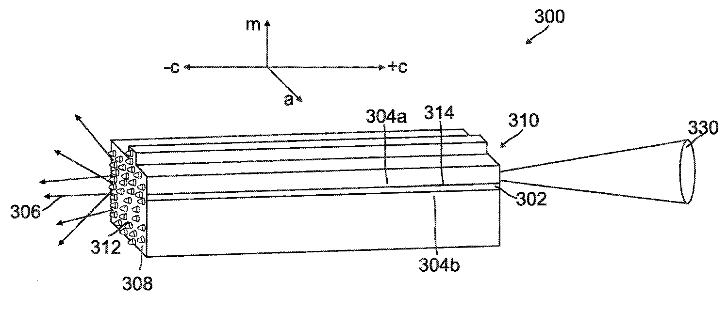
도 3a는 무극성 또는 반극성 (Ga,In,Al,B)N 또는 III-질화물 기반 광전자 소자(300)(예를 들어, 초발광 다이오드(SLD))의 개략도를 나타내며, 상기 광전자 소자는 활성 영역(302); 상기 활성 영역(302)으로부터 방사된 빛(306)의 광 가둠을 제공하는 광도파로 구조물(304a, 304b); 및 상기 광도파로 구조물(304a, 304b)의 반대 단부들 상의 제1 파세트(308) 및 제2 파세트(310)를 포함하는 한 쌍의 파세트들을 포함하고, 그에 따라 상기 제1 파세트(308)가 상기 제2 파세트(310)와 반대되며, 상기 제1 파세트(308) 및 상기 제2 파세트(310)는 반대 표면 극성을 갖고, 상기 제1 파세트(308)는 거칠어진 표면(312)을 갖는다. 거칠어진 제1 파세트(308)는 거칠어진 N-극성 면(N-polar plane)인 표면을 갖는 c- 파세트이고, 상기 제2 파세트는 c+ 파세트이다.3A shows a schematic of a nonpolar or semipolar (Ga, In, Al, B) N or III-nitride based optoelectronic device 300 (eg, a super light emitting diode (SLD)), the optoelectronic device being an
III-질화물의 -c, m, a, 및 +c 방향들이 또한 나타나고(도 3a의 직선들), 소자(300)는 m-방향을 따라 성장된다. 그러나, 상기 소자는 반극성 방향을 따라서 성장될 수도 있다. 상기 소자(300)의 성장면(314)(즉, 각각의 소자 층의 최종 성장면 또는 상부 표면)은 무극성 또는 반극성 면일 수 있다. 예를 들어, SLD들은 III-질화물의 a-면들 또는 III-질화물의 c-면과 인접한 III-질화물의 반-극성 면들(예를 들어, 20-21 또는 11-21 면들) 상에 제조될 수 있고, 그에 따라 무-극성 또는 반-극성 SLD들이 제조된다.The -c, m, a, and + c directions of III-nitride are also shown (straight lines in FIG. 3A), and
도 3b는 도 3a의 소자의 가로축 단면으로서, n-타입 층들(316), p-타입 층들(318), 및 제1 양자 배리어 층(320b)과 제2 양자 우물 배리어 층(320c) 사이에 개재된 양자 우물(320a)을 포함하는 활성 영역(302)을 도시하며, 양자 우물 층(320a)의 두께는 4 nm 이상이다.3B is a transverse cross-section of the device of FIG. 3A, interposed between n-
도 3a의 소자는, 블록(100) 및 (21)에 나타난 바와 같은, 표준 기술들을 사용하여 레이저 다이오드(LD)를 먼저 성장시키고 제조함으로써 제조된다. 구체적으로, AlGaN-클래딩-없는 LD 구조물이, 표준 유기-금속 화학 증착(metal-organic chemical vapor deposition)에 의해, 미츠비시 화학 회사에 의해 제조된 벌크 m-면 기판(예를 들어, m-면 GaN) 상에 성장된다(18) (또한 (22) 및 Daniel F. Feezell, Mathew C. Schmidt, Kwang Choong Kim, Robert M. Farrell, Daniel A. Cohen, James S. Speck, Steven P. DenBaars, and Shuji Nakamura에 의해 208년 2월 12일 출원된 "Al(x)Ga(1-x)N-CLADDING-FREE NONPOLAR GAN-BASED LASER DIODES AND LEDS,"라는 제목의, 대리인 사건 번호 30794.222-US-U1 (2007-424)인 미국 실용 출원 일련번호 제12/030,117호 참조). 상기 구조물은 (4-μm-두께의 Si-도핑된 GaN 클래딩 층, 이후 50 nm의 Si-도핑된 n-타입 InGaN 광도파로 층(304b)을 포함하는) n-타입 층들(316)로 구성된다. 비록 도 3b가 일 피리어드(period)를 나타내지만, 활성 영역(302)은 실제로 3 피리어드 InGaN/InGaN 다수 양자 우물 구조물로 구성되도록 제조된다(그러나, 임의의 수의 양자 우물들 또는 임의의 양자 우물 합성물, 예를 들어, InGaN/GaN 양자 우물들이 가능하다). 비의도적으로 도핑된 GaN 층이 활성 영역(302)의 상부 상에 성장되고, 이후 10-nm-두께의 Mg-도핑된 Al0 .25Ga0 .75N 전자 블로킹 층(electron blocking layer, 이라 'EBL'로 지칭함)이 뒤따른다. 상기 EBL 이후 (50 nm Mg-도핑된 p-타입 InGaN 광도파로 층(304a), 약 500-nm-두께의 Mg-도핑된 p-타입 GaN으로 구성된 상부 클래딩, 및 상기 구조물을 캡핑(capping)하는 100 nm Mg-도핑된 p++ 콘택 층을 포함하는) p-타입 층들(318)이 뒤따른다. c-방향을 따라 리지들(ridges)을 패터닝 및 건식 식각함으로써 4 μm 폭의 스트라이프 또는 리지(322)가 형성된다.The device of FIG. 3A is fabricated by first growing and fabricating a laser diode LD using standard techniques, as shown in
산화물 절연체(324)를 위해 표준 리프트오프(liftoff) 공정이 사용되었고, 이후 캐소드 전극들(326) 용 Pd/Au 금속 퇴적이 뒤따른다. 파세트들(308, 310)은 클리빙(cleaving)에 의해 형성되며, 그에 따라 500 μm의 캐비티 길이(cavity length)가 생기고, 인듐이 후면 애노드 전극(328)을 형성하는데 사용되었다. 이후, 블록(102)에 나타난 것처럼 제1 파세트(308)가 거칠게 된다. 빛(306)의 면-정렬 출력 전력(330)은 c+ 파세트(310)으로부터 측정될 수 있다.A standard liftoff process was used for the
도 3c 내지 도 3e는 소자의 SEM 이미지들로서, 도 3c는 KOH 처리 이전 소자의 -c 파세트를 나타내고, 도 3d는 KOH 처리 이후 -c 파세트를 나타내며(도 3a의 소자), 도 3e는 KOH 처리 이후 +c 파세트를 나타내고(도 3a의 소자), 도 3c는 표면 형태구조(surface morphology)를 나타내기 위해 40°각도에서 촬영되었다.3C-3E are SEM images of the device, FIG. 3C shows the -c facet of the device before KOH treatment, FIG. 3D shows the -c facet after the KOH treatment (device of FIG. 3A), and FIG. 3E shows KOH After treatment, the + c facet is shown (device of FIG. 3A), and FIG. 3C is photographed at 40 ° to show surface morphology.
상기 SEM 이미지들은 육각형 피라미드들(332)의 -c 파세트 상에서만의 형성을 나타내고, 거칠어진 표면은 0.1 내지 1.6 마이크로미터 사이의 베이스 지름(base diameter)를 갖는 육각형 피라미드들을 1개 이상 포함한다(육각형 피라미드의 베이스 지름은, n-타입 GaN 상에서 0.3 내지 1.6 μm, p-타입 GaN 상에서 100 내지 150 nm의 범위를 갖는다). 그러나, 거칠어진 표면은 (예를 들어, 가열 또는 PEC 식각을 사용한, 10 마이크로미터 이상의 베이스 지름을 포함하는) 임의의 특정 차수들 또는 모습들에 제한되지 않는다.The SEM images show the formation only on the -c facet of the
예를 들어, 도 3f는 거칠어진 표면이 베이스 지름(334) 및 높이(336)를 갖는 1개 이상의 구조물들(예를 들어, 원뿔들(332))을 가질 수 있음을 나타내고, 예를 들어 상기 베이스 지름(334)은 10 마이크로미터 이상일 수 있다. 상기 베이스 지름(334) 및/또는 높이(336)는, 구조물들이 SLD의 외부 빛을 산란시키는 빛의 파장과 충분히 근접할 수 있다. 도 3f는 또한 어떻게 구조물들이 육각형 베이스(340) 및 {10-1-1} 면 측벽들(342)을 갖는 육각형 피라미드들(338)일 수 있는지를 나타내고, 육각형 피라미드들(338)은 원뿔-형상(332)이다. 만일 측벽(342)이 {10-1-1} 면을 형성할 경우, {10-1-1} 면의 각도는 c-면에 대해 62도이다.For example, FIG. 3F shows that the roughened surface may have one or more structures (eg, cones 332) having a
일부 실시예들에서, c- 파세트(308)의 전체 표면은 원뿔들로 덮이고, 일부 실시예들에서, 더욱 큰 원뿔들(332)이 더 바람직하다.
In some embodiments, the entire surface of c − facet 308 is covered with cones, and in some embodiments,
소자 성능Device performance
도 4는 다른 구동 전류들(mA)에 대한 스펙트럼들을 나타내고(나노미터(nm)의 파장 대비 광 출력 강도, 임의 단위들(arbitrary units (arb. units)), 도 4a는 KOH 처리 이전의 4 μm 리지 레이저 다이오드(LD)를 나타내고(각각 175 mA, 190 mA, 및 210 mA의 구동 전류들에 대한 하부 커브로부터 상부 커브), 도 4b는, 면-정렬 방사에 대해, KOH 처리 이후의 동일한 소자(도 3a의 소자)를 나타내며(각각 15 mA, 45 mA, 105 mA, 180 mA, 255 mA, 및 315 mA의 구동 전류들에 대한 하부 커브로부터 상부 커브), 도 4c는 광도파로와 수직하고 기판 하부에서의 방사라는 점을 제외하고는 KOH 처리 이후의 동일한 소자(도 3a의 소자)를 나타낸다.FIG. 4 shows spectra for different drive currents (mA) (light output intensity versus wavelength in nanometers (arbitrary units (arb. Units)), FIG. 4A shows 4 μm before KOH treatment) The ridge laser diode (LD) is shown (upper curve from lower curve for drive currents of 175 mA, 190 mA, and 210 mA, respectively), and FIG. 4B shows the same device after KOH treatment for surface-aligned radiation ( 3a) (upper curve from lower curve for drive currents of 15 mA, 45 mA, 105 mA, 180 mA, 255 mA, and 315 mA, respectively), and FIG. 4C is perpendicular to the optical waveguide and lower substrate The same device (device of FIG. 3A) after KOH treatment is shown except that it is radiation at.
KOH 처리 이전, 레이징 피크들은 436.8 nm의 피크 파장과 함께, 190 mA 로 낮은 주입 전류들에서 관측되었고(9.05 kA/cm2), 레이저 다이오드(LD)에 대한 반값 전폭(full width at half maximum intensity, 이하 'FWHM'으로 지칭함)은 임계(threshold) 바로 위 190 mA에서 0.3 nm 이다.Prior to the KOH treatment, the rising peaks were observed at injection currents as low as 190 mA, with a peak wavelength of 436.8 nm (9.05 kA / cm 2 ), and full width at half maximum intensity for the laser diode (LD). , Hereinafter referred to as 'FWHM') is 0.3 nm at 190 mA just above the threshold.
광도파로 내 유도된 방사의 존재 때문에, KOH 처리 이후 소자에 대한 스펙트럼 폭은 구동 전류의 증가에 따라 좁아지지만, 나타난 전류 범위에서는 레이징에 기인한 스펙트럼들 내 가파른 피크가 관측되지 않는다. SLD의 최소 FWHM은 315 mA에서 9 nm 이고, 이는 LD의 그것보다 한 오더의 크기 정도로 높으며, 피크 파장은 439 nm 이다.
Because of the presence of induced radiation in the optical waveguide, the spectral width for the device after the KOH treatment narrows with increasing drive current, but no steep peaks in the spectra due to lasing are observed in the current range shown. The minimum FWHM of the SLD is 9 nm at 315 mA, which is on the order of magnitude higher than that of the LD, with a peak wavelength of 439 nm.
도 5는 도 3a의 소자의 FWHM을 측정하고, 소자의 거칠어진 표면이, SLD에 의해 방사된 빛의 FWHM이 거칠게 하는 단계를 수행하지 않는 소자보다 적어도 10배 더 크도록(예를 들어, LD의 FWHM보다 10배 큰 SLD의 FWHM) 할 수 있다는 것을 도시한다. 도 5에서, SLD는 8 nm의 최소 FWHM을 나타내고, 반면에 전형적인 LD FWHM은 0.2 nm 이다. SLD는 광 캐비티(optical cavity) 내 공진으로 인해 강한 파장 선택을 보증하지 않는다.
FIG. 5 measures the FWHM of the device of FIG. 3A and the roughened surface of the device is at least 10 times larger than the device that does not perform the step of roughening the FWHM of light emitted by the SLD (eg, LD It can be seen that the FWHM of SLD) is 10 times larger than the FWHM. In FIG. 5, SLD shows a minimum FWHM of 8 nm, while a typical LD FWHM is 0.2 nm. SLD does not guarantee strong wavelength selection due to resonance in the optical cavity.
도 6은 KOH 처리 이전의 LD, 및 이후의 SLD의 L-I 특성들을 나타내고(도 3a의 소자), 점선은 LD 데이터에 대한 시각적 안내이고 실선은 SLD 데이터에 일치하는 지수 함수이다. KOH 처리 이전, 상기 L-I 커브는 임계 이상에서 출력 전력에서의 선형 증가와 함께 매우 가파른 레이징 임계(lasing threshold)를 나타냈다.FIG. 6 shows the L-I characteristics of LD before KOH treatment and subsequent SLD (device of FIG. 3A), dotted lines are visual guidance for LD data and solid lines are exponential functions consistent with SLD data. Prior to KOH treatment, the L-I curve exhibited a very steep lasing threshold with a linear increase in output power above the threshold.
+c 파세트 외부에서 출력된 SLD의 출력 전력은 약 5 mW에 달했다. KOH 처리 이후의 출력 전력은 선형 이득 영역(linear gain regime) 내의 SLD로 예상한 바와 같이 전류의 함수로서 지수적으로 증가하였다.
The output power of the SLD output from outside the + c facet was about 5 mW. The output power after KOH treatment increased exponentially as a function of current as expected with SLD in a linear gain regime.
도 7에서, 도 7a는 배치된 검출기의 개략적인 도면을 나타내고, 도 7b는 (도 3a의 소자를 사용한) SLD 방사의 전류의 함수로서의 스펙트럼 통합 강도(spectrally integrated intensity)를 나타내고, +c 파세트에서의 면-정렬(700) 방사, 후면(702)으로부터의 방사가 측정되며, 100 mA 이상의 전류 값들과 상응하는 데이터에 일치하는 지수(면-정렬) 및 선형(후면) 커브도 나타난다. 상기 통합 강도는, 광도파로와 수직인 소자 하부(후면(70)) 및 c+ 파세트(면-정렬)에서 면-정렬(700)로 위치된 검출기에 연결된 광섬유를 사용하여 측정되었다. 상기 면-정렬(700) 방사는 광도파로 내 증폭으로 인한 유도 및 자연 방사 모두를 포함하고, 반면에 후면(702) 방사는 기판을 통해 전달된 유도 방사만을 측정한다.In FIG. 7, FIG. 7A shows a schematic view of the detector placed, FIG. 7B shows the spectrally integrated intensity as a function of the current of the SLD emission (using the device of FIG. 3A), and + c facet The plane-aligned 700 radiation at, the radiation from the
후면 방사로부터의 면-정렬 방사의 전환(divergence)은 100 mA 바로 미만에서의 초발광의 개시를 의미한다. 이는 이득으로 인해 일어나고, 광도파로를 따른 유도 방사로부터 발생되어, 측정된 면-정렬 강도가 기하급수적으로 증가하게 되고, 반면에 자연 방사만으로 구성된 후면 방사는 선형을 유지한다. 상기 초발광의 개시 하부에서, 면-정렬 및 후면 방사 모두가, 방사 메커니즘의 변화로 인해, 상기 개시 상부의 상기 데이터 일치들(fits)로부터 선형적으로 전환됨에 또한 유의한다.Divergence of plane-aligned radiation from backside radiation refers to the onset of superluminescence just below 100 mA. This occurs due to the gain and arises from induced radiation along the optical waveguide, so that the measured plane-aligned intensity increases exponentially, while the backside radiation consisting of only natural radiation remains linear. It is also noted that under the onset of the superluminescence, both face-alignment and backside radiation is linearly converted from the data fits on the top of the initiation due to changes in the radiation mechanism.
(Ga,In,Al,B)N SLD들은 벌크 무극성 또는 반극성 기판들(예를 들어, III-질화물 또는 GaN 기판들) 상에서 가장 잘 제조될 것인데, 이러한 기판들 상에서의 에피택셜 성장으로 인해 강화된 광 및 전기 특성들의 이점이 달성된다. 그러나, 본 발명은 임의의 기판 상에 성장된 c-면 파세트들을 갖는 임의의 소자에 대해서도 사용될 수도 있다.(Ga, In, Al, B) N SLDs will be best fabricated on bulk nonpolar or semipolar substrates (e.g., III-nitride or GaN substrates), strengthened due to epitaxial growth on these substrates The advantages of the optical and electrical characteristics achieved are achieved. However, the present invention may be used for any device having c-plane facets grown on any substrate.
본 발명의 SLD들의 응용분야들은, 고전력 방향성 고상 조명, 조명과 연결된 섬유, 및 조절가능한 미러 손실을 갖는 청색에서의 녹색의(혹은 가능하다면 이를 넘는) 스펙트럼 영역에서의 피코 프로젝터들(pico projectors) 및 레티날 스캐닝 디스플레이들(retinal scanning displays)의 광원들을 포함하지만, 이에 제한되지는 않는다.
Applications of the SLDs of the present invention include pico projectors in the spectral region of green (or more than possible) in blue with high power directional solid state illumination, fiber associated with illumination, and adjustable mirror loss and Includes, but is not limited to, light sources of retinal scanning displays.
가능한 수정들Possible modifications
결정 화학 식각 공정은 제1 파세트(c- 파세트)를 거칠게 하는데 사용될 수 있다. 예를 들어, 결정 화학 식각 공정은, 가열되거나 상온인 상태에서 KOH를 사용할 수 있다. 그러나, 결정 식각을 일으키는 다른 습식 식각 공정들도 또한 결정 화학 식각 공정으로서 사용될 수 있다. 전해질의 농도 및 식각 시간은 제1 파세트(308)의 총 파세트 거칠기, 밀도, 및 피쳐 크기를 제어하도록 변화될 수 있다.Crystalline chemical etching processes can be used to roughen the first facet (c-facet). For example, the crystal chemical etching process may use KOH while heated or at room temperature. However, other wet etching processes that cause crystal etching may also be used as the crystal chemical etching process. The concentration and etching time of the electrolyte may be varied to control the total facet roughness, density, and feature size of the
따라서, 결정 식각 공정으로서의 PEC 식각 기술들의 사용을 포함하는, 결정 식각을 일으키는 임의의 식각 화학 반응은 본 발명의 범위에 포함된다. PEC 식각 속도들은 상부면이 적절하게 보호되는 경우 전형적으로 비-조명 식각(non-illuminated etching)보다 1 내지 2 오더의 크기만큼 더 빠르고 더욱 높은 처리량을 제공할 수 있다.Thus, any etching chemical reaction that results in crystal etching, including the use of PEC etching techniques as a crystal etching process, is within the scope of the present invention. PEC etch rates can typically provide one to two orders of magnitude faster and higher throughput than non-illuminated etching if the top surface is properly protected.
AZ 726 MIF와 같은 일부 포토레지스트 현상액들도 상기 식각 공정 동안(예를 들어, 결정 화학 식각 공정 동안) 사용될 수 있다. 예를 들어, 일부 포토레지스트 현상액들은 N-표면(face) GaN을 결정 식각하는데도 또한 사용될 수 있다. N-표면 GaN의 일반적인 화학 반응성 때문에, 결정 식각을 일으킬 다른 식각 화학반응들이 존재할 것이고, 상기 다른 식각 화학반응들은 전술한 바와 같이 비-반사 파세트를 형성하는데 또한 사용될 수 있다.Some photoresist developers, such as AZ 726 MIF, may also be used during the etching process (eg, during the crystalline chemical etching process). For example, some photoresist developers may also be used to crystal etch N-face GaN. Because of the general chemical reactivity of N-surface GaN, there will be other etching chemistries that will cause crystal etching, which may also be used to form non-reflective facets as described above.
따라서, 본 발명의 광전자 소자는, 활성 영역, 상기 활성 영역으로부터 방사된 빛의 광 가둠을 제공하는 광도파로 구조물; 반대되는 표면 극성을 갖는, 상기 소자의 반대 단부들 상의 한 쌍의 파세트들을 포함할 수 있다. 상기 소자는 무극성 또는 반극성 (Ga,In,Al,B)N 기반 소자일 수 있다(즉, 상기 소자의 성장면은 전형적으로 무극성 또는 반극성이고 표면 극성들은 전형적으로 c+ 및 c- 파세트와 상응한다).Accordingly, the optoelectronic device of the present invention comprises: an optical waveguide structure providing an active region, a confinement of light emitted from the active region; It may comprise a pair of facets on opposite ends of the device, with opposite surface polarity. The device may be a nonpolar or semipolar (Ga, In, Al, B) N based device (ie, the growth surface of the device is typically nonpolar or semipolar and surface polarities are typically c + and c − facets Corresponds to).
상기 파세트들은, c+ 파세트로부터의 광 출력에 대한 양호한 방향성 및 원 전계 패턴(far field pattern, FFP)을 달성하도록 클리빙(cleaving)함으로써 형성될 수 있다. 상기 파세트들은 건식 식각, 집속 이온빔(focussed ion beam, FIB) 기반 기술들, 연마 또는 다른 방법들에 의해 형성될 수도 있다. 파세트 일방에 대해 출력 파세트의 반사도를 증가시키거나 또는 감소시키기 위해 또는 카타스트로픽 광손상(catastrophic optical damage, COD)을 억제하기 위해, 파세트 코팅이 사용될 수 있다.The facets can be formed by cleaving to achieve good directionality and far field pattern (FFP) for light output from the c + facet. The facets may be formed by dry etching, focused ion beam (FIB) based techniques, polishing or other methods. Facet coatings can be used to increase or decrease the reflectivity of the output facet relative to either facet or to suppress catastrophic optical damage (COD).
이후, 파세트들 중 하나는 결정 화학 식각 공정에 의해 거칠게 될 수 있고, 여기서 상기 거칠게된 파세트는 c- 질소-극성 (N-극성) 면이다.One of the facets can then be roughened by a crystalline chemical etching process, where the roughened facet is a c - nitrogen-polar (N-polar) plane.
예를 들어, 광도파로 구조물은 내부 손실을 감소시키기 위해 굴절률 가이드 또는 이득 가이드를 활용할 수 있다.For example, an optical waveguide structure may utilize a refractive index guide or gain guide to reduce internal losses.
본 발명은 너무 많은 반사들이 있는 경우 +c 파세트 상에 비-반사 코팅을 놓도록 하는 선택예를 포함한다. 전면(front side)을 코팅하는 것 또한 소자 성능을 개선시킬 수 있다.The present invention includes an option to place a non-reflective coating on the + c facet when there are too many reflections. Coating the front side can also improve device performance.
또한, 스트라이프(332)는 양 파세트들의 반사들을 더욱 감소시기 위해 파세트들 사이에서 각도를 갖도록 놓여질 수 있고, 이는 성능을 개선시킬 수 있다.
In addition, the
이점들 및 개선들Advantages and improvements
본 발명은 신규한 메커니즘인, (Ga,In,Al,B)N 초발광 다이오드들(SLDs)에의 사용에 적합한 비-반사 파세트를 형성하기 위한, 결정 식각된 광 추출 원뿔들을 특징적으로 다루고 있다. 이 습식 식각 단계는 표준 레이저 다이오드(LD) 제조 공정에 더해질 수 있으며, 그에 따라 최소한의 공정 전개만으로 SLD 제조가 가능하다. 예를 들어, 본 발명은, 단일의 상대적으로 저렴하고 직접적인 공정 단계만의 추가로, c-면 클리빙된 파세트들을 갖는, 임의의 무극성 (Ga,In,Al,B)N LD 공정으로부터의 SLD들의 제조를 가능케 한다. 저반사 파세트를 형성하는 이 방법은 웨이퍼 상의 소자 패킹 밀도(device packing density)에서의 어떠한 희생도 요구하지 않고, 일반 레이저 공정과 호환되지 않는 임의의 공정 단계들을 요구하지 않는다. 이 기술은 임의의 무극성 (Ga,In,Al,B)N 레이저 공정이 임의의 공정 단계들을 변화시키거나 재-최적화할 필요 없이 SLD들의 제조에 직접 적용되는 것을 허용한다. 따라서, 배치 기반의 습식 식각 단계인 이 기술의 산업적 적용은, 다른 제조 방법들에 비해 낮은 비용으로 이루어지는 것을 약속한다.The present invention features a crystalline etched light extraction cone for forming a non-reflective facet suitable for use with (Ga, In, Al, B) N super light emitting diodes (SLDs), a novel mechanism. . This wet etching step can be added to a standard laser diode (LD) manufacturing process, thus enabling SLD manufacturing with minimal process deployment. For example, the present invention from any nonpolar (Ga, In, Al, B) N LD process with c-plane cleaved facets, in addition to only a single relatively inexpensive and direct process step. It allows the manufacture of SLDs. This method of forming low reflection facets does not require any sacrifice in device packing density on the wafer and does not require any process steps that are incompatible with normal laser processes. This technique allows any nonpolar (Ga, In, Al, B) N laser process to be applied directly to the manufacture of SLDs without the need to change or re-optimize any process steps. Thus, the industrial application of this technique, a batch-based wet etching step, promises to be made at a lower cost than other manufacturing methods.
SLD들은 그것들의 상대적으로 큰 스펙트럼 폭, 방향성을 갖는 출력 및 상대적으로 높은 전력으로 인해 피코 프로젝터들 및 레티날 스캐닝 디스플레이들의 광원으로서 동작할 수 있다(9).SLDs can act as a light source for pico projectors and retinal scanning displays due to their relatively large spectral width, directional output and relatively high power (9).
본 발명은 제조의 용이성 및 확장성(scalability)과 같은 SLD들의 제조의 이점을 제공한다.
The present invention provides the advantages of manufacturing SLDs such as ease of manufacture and scalability.
참조들References
이하의 참조들은 전체로서 본원에 참조 병합된다.The following references are hereby incorporated by reference in their entirety.
(1) "AlGaN-Cladding-Free Nonpolar InGaN/GaN Laser Diodes," by Feezell, D. F., et al., Jpn. J. Appl. Phys., Vol. 46, pp. L284-L286 (2007). (1) "AlGaN-Cladding-Free Nonpolar InGaN / GaN Laser Diodes," by Feezell, D. F., et al., Jpn. J. Appl. Phys., Vol. 46, pp. L284-L286 (2007).
(2) "Continuous-wave Operation of AlGaN-cladding-free Nonpolar m-Plane InGaN/GaN Laser Diodes," by Farrell, R. M., et al., Jpn. J. Appl. Phys., Vol. 46, pp. L761-L763 (2007).(2) "Continuous-wave Operation of AlGaN-cladding-free Nonpolar m-Plane InGaN / GaN Laser Diodes," by Farrell, R. M., et al., Jpn. J. Appl. Phys., Vol. 46, pp. L761-L763 (2007).
(3) "Reduction of Threshold Current Density of Wurtzite GaN/AlGaN Quantum Well Lasers by Uniaxial Strain in (0001) Plane," by Suzuki, Masakatsu and Uenoyama, Takeshi.: The Japan Society of Applied Physics, Jpn. J. Appl. Phys., Vol. 35, pp. L953-L955 (1996).(3) "Reduction of Threshold Current Density of Wurtzite GaN / AlGaN Quantum Well Lasers by Uniaxial Strain in (0001) Plane," by Suzuki, Masakatsu and Uenoyama, Takeshi .: The Japan Society of Applied Physics, Jpn. J. Appl. Phys., Vol. 35, pp. L953-L955 (1996).
(4) "Continuous-Wave Operation of m-Plane InGaN Multiple Quantum Well Laser Diodes," by Okamoto, Kuniyoshi, et al.: The Japan Society of Applied Physics, Japanese Journal of Applied Physics, Vol. 46, pp. L187-L189 (2007).(4) "Continuous-Wave Operation of m-Plane InGaN Multiple Quantum Well Laser Diodes," by Okamoto, Kuniyoshi, et al .: The Japan Society of Applied Physics, Japanese Journal of Applied Physics, Vol. 46, pp. L187-L189 (2007).
(5) "Roughening Hexagonal Surface Morphology on Laser Lift-Off (LLO) N-Face GaN with Simple Photo-Enhanced Chemical Wet Etching," by Gao, Yan, et al., Jap. J. Appl. Phys., Vol. 43, p. L637 (2004).(5) "Roughening Hexagonal Surface Morphology on Laser Lift-Off (LLO) N-Face GaN with Simple Photo-Enhanced Chemical Wet Etching," by Gao, Yan, et al., Jap. J. Appl. Phys., Vol. 43, p. L637 (2004).
(6) "Dislocation- and crystallographic-dependent photoelectrochemical wet etching of gallium nitride," by Gao, Y., et al.: AIP, Applied Physics Letters, Vol. 84, pp. 3322-3324 (2004).(6) "Dislocation- and crystallographic-dependent photoelectrochemical wet etching of gallium nitride," by Gao, Y., et al .: AIP, Applied Physics Letters, Vol. 84, pp. 3322-3324 (2004).
(7) "A stripe-geometry double-heterostructure amplified-spontaneous-emission (superluminescent) diode," by Lee, Tien-Pei, Burrus, C. and Miller, B., IEEE J. Quantum. Electron., Vol. 9, pp. 820-828 (1973).(7) "A stripe-geometry double-heterostructure amplified-spontaneous-emission (superluminescent) diode," by Lee, Tien-Pei, Burrus, C. and Miller, B., IEEE J. Quantum. Electron., Vol. 9, pp. 820-828 (1973).
(8) "Cone-shaped surface GaN-based light-emitting diodes," Fujii, T., et al., physica status solidi (c), Vol. 2, pp. 2836-2840 (2005).(8) "Cone-shaped surface GaN-based light-emitting diodes," Fujii, T., et al., Physica status solidi (c), Vol. 2, pp. 2836-2840 (2005).
(9) "Development of a commercial retinal scanning display," by Johnston, Richard S. and Willey, Stephen R.: SPIE, Proc. SPIE, Vol. 2465, pp. 2-13 (1995).(9) "Development of a commercial retinal scanning display," by Johnston, Richard S. and Willey, Stephen R .: SPIE, Proc. SPIE, Vol. 2465, pp. 2-13 (1995).
(10) "High-Efficiency Continuous-Wave Operation of Blue-Green Laser Diodes Based on Nonpolar m-Plane Gallium Nitride," by Okamoto, Kuniyoshi, Tanaka, Taketoshi and Kubota, Masashi., Appl. Phys. Express, Vol. 1, p. 072201 (2008).(10) "High-Efficiency Continuous-Wave Operation of Blue-Green Laser Diodes Based on Nonpolar m-Plane Gallium Nitride," by Okamoto, Kuniyoshi, Tanaka, Taketoshi and Kubota, Masashi., Appl. Phys. Express, Vol. 1, p. 072201 (2008).
(11) "Nonpolar m-plane InGaN multiple quantum well laser diodes with a lasing wavelength of 499.8 nm," by Okamoto, Kuniyoshi, et al. s.l., AIP, Appl. Phys. Lett., Vol. 94, p. 071105 (2009).(11) "Nonpolar m-plane InGaN multiple quantum well laser diodes with a lasing wavelength of 499.8 nm," by Okamoto, Kuniyoshi, et al. s.l., AIP, Appl. Phys. Lett., Vol. 94, p. 071105 (2009).
(12) "Increase in the extraction efficiency of GaN-based light-emitting diodes via surface roughening," Fujii, T., et al., AIP, Applied Physics Letters, Vol. 84, pp. 855-857 (2004).(12) "Increase in the extraction efficiency of GaN-based light-emitting diodes via surface roughening," Fujii, T., et al., AIP, Applied Physics Letters, Vol. 84, pp. 855-857 (2004).
(13) 미국 특허 일련번호 제4,901,123호, 1990년 2월 13일 등록됨, by Noguchi et. al.(13) US Patent Serial No. 4,901,123, registered February 13, 1990, by Noguchi et. al.
(14) 미국 특허 일련번호 제5,223,722 호, 1993년 6월 29일 등록됨, by Nagai et. al.(14) US Patent Serial No. 5,223,722, registered June 29, 1993, by Nagai et. al.
(15) 미국 특허 일련번호 제4,896,195호, 1990년 1월 23일 등록됨, by Jansen et. al.(15) US Pat. No. 4,896,195, registered January 23, 1990, by Jansen et. al.
(16) 미국 특허 일련번호 제4,958,355호, 1990년 9월 18일 등록됨, by Alphonse et. al.(16) US Pat. No. 4,958,355, registered September 18, 1990, by Alphonse et. al.
(17)"m-plane GaN-based Blue Superluminescent Diodes Fabricated Using Selective Chemical Wet Etching," by Matthew T. Hardy, Kathryn M. Kelchner, You-Da Lin, Po Shan Hsu, Kenji Fujito, Hiroaki Ohta, James S. Speck, Shuji Nakamura, and Steven P. DenBaars.(17) "m-plane GaN-based Blue Superluminescent Diodes Fabricated Using Selective Chemical Wet Etching," by Matthew T. Hardy, Kathryn M. Kelchner, You-Da Lin, Po Shan Hsu, Kenji Fujito, Hiroaki Ohta, James S. Speck, Shuji Nakamura, and Steven P. DenBaars.
(18) K. M. Kelchner, Y. D. Lin, M. T. Hardy, C. Y. Huang, P. S. Hsu, R. M. Farrell, D. A. Haeger, H. C. Kuo, F. Wu, K. Fujito, D. A. Cohen, A. Chakraborty, H. Ohta, J. S. Speck, S. Nakamura and S. P. DenBaars: Appl. Phys. Express 2 (2009) 071003.(18) KM Kelchner, YD Lin, MT Hardy, CY Huang, PS Hsu, RM Farrell, DA Haeger, HC Kuo, F. Wu, K. Fujito, DA Cohen, A. Chakraborty, H. Ohta, JS Speck, S Nakamura and SP DenBaars: Appl. Phys. Express 2 (2009) 071003.
(20). Shuji Nakamura에 의해 제공된 프리젠테이션 슬라이드들, 제목 "An overview of Laser Diodes (LDs) and Light Emitting Diodes (LEDs) Research at SSLEC," at the 2009 Annual Review for Solid State Lighting and Energy Center (SSLEC), University of California, Santa Barbara (2009년 11월 5일). (20). Presentation slides provided by Shuji Nakamura, titled "An overview of Laser Diodes (LDs) and Light Emitting Diodes (LEDs) Research at SSLEC," at the 2009 Annual Review for Solid State Lighting and Energy Center (SSLEC), University of California, Santa Barbara (5 November 2009).
(21). Matthew T. Hardy에 의해 제공된 프리젠테이션 슬라이드들, 제목 "Backend Processing for m-plane Cleaved Facet Laser Diodes and Superluminescent Diodes," at the 2009 Annual Review for SSLEC, University of California, Santa Barbara (2009년 11월 6일). (21). Presentation slides provided by Matthew T. Hardy, titled "Backend Processing for m-plane Cleaved Facet Laser Diodes and Superluminescent Diodes," at the 2009 Annual Review for SSLEC, University of California, Santa Barbara (6 November 2009 ).
(22) Kate Kelchner에 의해 제공된 프리젠테이션 슬라이드들, at the 2009 Annual Review for SSLEC, 제목 "Continuous Wave Technology for Pure Blue Laser Diodes on Nonpolar m-plane GaN", 2009년 11월 6일, University of California, Santa Barbara.
(22) Presentation slides provided by Kate Kelchner, at the 2009 Annual Review for SSLEC, entitled "Continuous Wave Technology for Pure Blue Laser Diodes on Nonpolar m-plane GaN", November 6, 2009, University of California, Santa Barbara.
결론conclusion
이 부분에서는 본 발명의 바람직한 실시예의 설명을 결론짓기로 한다. 전술한 본 발명의 하나 이상의 실시예들의 설명은 도시 및 설명의 목적으로 나타난 것이다. 배타적이거나 개시된 정확한 형태로 반 발명의 제한하려는 의도가 아니다. 전술한 교시들에 비추어 많은 수정들 및 변화들이 가능하다. 본 발명의 범위는 이 상세한 설명에 제한되는 것이 아니고, 오히려 여기에 첨부된 청구항들에 의해 발명의 범위가 제한되는 것으로 의도된다.This section concludes the description of the preferred embodiment of the present invention. The foregoing description of one or more embodiments of the invention has been presented for purposes of illustration and description. It is not intended to be exhaustive or to limit the invention to the precise forms disclosed. Many modifications and variations are possible in light of the above teachings. The scope of the invention is not limited to this detailed description, but rather is intended to be limited by the claims appended hereto.
Claims (35)
활성 영역;
상기 활성 영역으로부터 방사된 빛의 광 가둠(optical confinement)을 제공하는 광도파로 구조물; 및
상기 광도파로 구조물의 반대 단부들 상의 제1 파세트(facet) 및 제2 파세트를 포함하고,
상기 제1 파세트 및 상기 제2 파세트는 반대되는 표면 극성을 갖고,
상기 제1 파세트는 거칠어진 표면을 갖는 것을 특징으로 하는 광전자 소자.Nonpolar or semipolar III-nitride based optoelectronic devices,
Active area;
An optical waveguide structure providing optical confinement of light emitted from the active region; And
A first facet and a second facet on opposite ends of the optical waveguide structure,
The first facet and the second facet have opposite surface polarities,
And the first facet has a roughened surface.
상기 제1 파세트는 상기 III-질화물 소자의 거칠어진 c- 파세트, c- 면(plane), 또는 N-표면(face)을 포함하고,
상기 제2 파세트는 상기 III-질화물 소자의 c+ 파세트, c+ 면, III-표면, 또는 Ga 표면을 포함하는 것을 특징으로 하는 광전자 소자.The method of claim 1,
It includes a surface (plane), or N- surface (face), - the first wave set rough Jin c of the III- nitride devices-wave set, c
The second wave set optoelectronic device comprises a wave set of c + III- nitride devices, c + plane, III- surface, or Ga surface.
상기 거칠어진 표면은 습식 식각된 표면인 것을 특징으로 하는 광전자 소자.The method of claim 2,
And said roughened surface is a wet etched surface.
상기 거칠어진 표면은 결정 식각된 표면인 것을 특징으로 하는 광전자 소자.The method of claim 2,
The roughened surface is an optoelectronic device, characterized in that the crystal etched surface.
상기 거칠어진 표면은 광전화학(PEC) 식각된 표면인 것을 특징으로 하는 광전자 소자.The method of claim 2,
And said roughened surface is a photochemical (PEC) etched surface.
상기 거칠어진 표면은 거칠어진 클리빙된 표면이고,
상기 제2 파세트는 클리빙된 표면을 가지는 것을 특징으로 하는 광전자 소자.The method of claim 2,
The roughened surface is a roughened cleaved surface,
And said second facet has a cleaved surface.
상기 거칠어진 표면은 상기 광도파로 구조물의 평면-정렬(in-plane) c-축을 따른 광 귀환을 억제하는 것을 특징으로 하는 광전자 소자.The method of claim 2,
Wherein the roughened surface inhibits optical feedback along the in-plane c-axis of the optical waveguide structure.
상기 거칠어진 표면은 지름 및 높이를 갖는 하나 이상의 구조물들을 포함하고,
상기 지름 및 상기 높이는 상기 구조물들이 상기 광도파로의 외부 빛을 산란시키는 빛의 파장과 충분히 근접한 것을 특징으로 하는 광전자 소자.The method of claim 2,
The roughened surface comprises one or more structures having a diameter and a height,
The diameter and the height are sufficiently close to the wavelength of light that the structures scatter outside light of the optical waveguide.
상기 거칠어진 표면은 0.1 내지 10 마이크로미터들 사이의 지름을 갖는 하나 이상의 육각형 피라미드들을 포함하는 것을 특징으로 하는 광전자 소자.The method of claim 2,
Wherein the roughened surface comprises one or more hexagonal pyramids having a diameter between 0.1 and 10 micrometers.
출력 젼력은 적어도 5 밀리와트인 것을 특징으로 하는 광전자 소자.The method of claim 2,
Optoelectronic device, characterized in that the output power is at least 5 milliwatts.
상기 소자는 초발광 다이오드(superluminescent diode, SLD)인 것을 특징으로 하는 광전자 소자.The method of claim 2,
The device is an optoelectronic device, characterized in that the superluminescent diode (SLD).
상기 거칠어진 표면은, 상기 초발광 다이오드의 선형 이득 구간(linear gain regime)에서, 상기 초발광 다이오드의 출력 전력이 증가하는 구동 전류에 따라 기하급수적으로 증가하도록 하는 것을 특징으로 하는 광전자 소자.The method of claim 11,
The roughened surface is an optoelectronic device, characterized in that in the linear gain regime of the super light emitting diode, the output power of the super light emitting diode increases exponentially with increasing drive current.
상기 거칠어진 표면은, 상기 초발광 다이오드에 의해 방사된 빛의 반값 전폭(full width at half maximum)이 거칠게 하는 단계를 수행하지 않는 소자의 경우보다 적어도 10배 더 크게 하는 것을 특징으로 하는 광전자 소자.The method of claim 11,
Wherein the roughened surface is at least 10 times larger than a device that does not perform a step of roughening the full width at half maximum of the light emitted by the super light emitting diode.
상기 초발광 다이오드는 청색광을 방사하고,
상기 거칠어진 표면은 상기 빛의 반값 전폭이 9 nm 보다 크게 하는 것을 특징으로 하는 광전자 소자.The method of claim 11,
The super light emitting diode emits blue light,
The roughened surface is an optoelectronic device, characterized in that the full width at half maximum of the light is greater than 9 nm.
상기 광도파로 구조물은 내부 손실을 감소시키기 위해 굴절률 가이드(index guiding) 또는 이득 가이드(gain guiding)를 활용하는 것을 특징으로 하는 광전자 소자.The method of claim 1,
And the optical waveguide structure utilizes an index guiding or a gain guiding to reduce internal loss.
제1 무극성 또는 반극성 III-질화물 기반 광전자 소자를 얻는 단계로서, 상기 광전자 소자는 활성 영역, 상기 활성 영역으로부터 방사된 빛의 광 가둠(optical confinement)을 제공하는 광도파로 구조물, 및 상기 광도파로 구조물의 반대 단부들 상의 제1 파세트(facet) 및 제2 파세트를 포함하고, 상기 제1 파세트 및 상기 제2 파세트는 반대되는 표면 극성을 갖는 것을 특징으로 하는 단계; 및
상기 제1 파세트의 표면을 거칠게 하는 단계를 포함하고,
상기 거칠게 하는 단계로 인해, 제2 무극성 또는 반극성 III-질화물 기반 광전자 소자가 제조되는 것을 특징으로 광전자 소자의 제조 방법.A method of making a nonpolar or semipolar III-nitride based optoelectronic device,
Obtaining a first nonpolar or semipolar III-nitride based optoelectronic device, the optoelectronic device comprising: an optical waveguide structure providing optical confinement of an active region, light emitted from the active region, and the optical waveguide structure A first facet and a second facet on opposite ends of the facet, wherein the first facet and the second facet have opposite surface polarities; And
Roughening the surface of the first facet,
Due to the roughening step, a second nonpolar or semipolar III-nitride based optoelectronic device is produced.
상기 제1 파세트는 상기 III-질화물 소자의 거칠어진 c- 면(plane), c- 파세트(facet), 또는 N-표면(face)을 포함하고,
상기 제2 파세트는 상기 III-질화물 소자의 c+ 파세트, c+ 면, Ga 표면, 또는 III-표면을 포함하는 것을 특징으로 하는 광전자 소자의 제조 방법.The method of claim 16,
The first facet comprises a roughened c - plane, c - facet, or N - face of the III-nitride device,
Wherein said second facet comprises a c + facet, a c + face, a Ga surface, or a III-surface of said III-nitride device.
상기 거칠게 하는 단계는 결정 식각을 일으키는 습식 식각에 의한 것을 특징으로 하는 광전자 소자의 제조 방법.18. The method of claim 17,
The roughening step is a method for manufacturing an optoelectronic device, characterized in that by wet etching to cause a crystal etching.
식각 시간 및 상기 습식 식각에서 사용되는 전해액의 농도는, 상기 제1 파세트의 총 파세트 거칠기, 밀도, 및 피쳐 크기(feature size)를 제어하도록 변화되는 것을 특징으로 하는 광전자 소자의 제조 방법.19. The method of claim 18,
The etching time and the concentration of the electrolyte used in the wet etching are changed to control the total facet roughness, density, and feature size of the first facet.
상기 거칠게 하는 단계는 결정 화학 식각 공정에 의한 것을 특징으로 하는 광전자 소자의 제조 방법.18. The method of claim 17,
The roughening step is a method of manufacturing an optoelectronic device, characterized in that by the crystal chemical etching process.
상기 결정 화학 식각 공정은 가열되거나 상온인 상태에서 KOH를 사용하는 것을 특징으로 하는 광전자 소자의 제조 방법.21. The method of claim 20,
The crystal chemical etching process is a method for manufacturing an optoelectronic device, characterized in that using KOH in a heated or room temperature state.
상기 결정 화학 식각 공정 동안 AZ 726 MIF를 포함하는 포토레지스트 현상액이 사용되는 것을 특징으로 하는 광전자 소자의 제조 방법.21. The method of claim 20,
A photoresist developer comprising AZ 726 MIF is used during the crystal chemical etching process.
상기 거칠게 하는 단계는 광전화학(PEC) 식각에 의한 것을 특징으로 하는 광전자 소자의 제조 방법.18. The method of claim 17,
The roughening step is a method of manufacturing an optoelectronic device, characterized in that by the photochemical (PEC) etching.
상기 제1 및 제2 파세트들은 상기 거칠게 하는 단계 전에 클리빙(cleaving)함으로써 형성되고, 그에 따라 상기 제2 파세트는 클리빙된 표면을 가지며 상기 거칠어진 표면은 클리빙된 상기 제1 파세트를 거칠게 함으로써 형성되는 것을 특징으로 하는 광전자 소자의 제조 방법.18. The method of claim 17,
The first and second facets are formed by cleaving before the roughening step such that the second facet has a cleaved surface and the roughened surface is cleaved first facet A method of manufacturing an optoelectronic device, characterized in that it is formed by roughening.
상기 거칠게 하는 단계 이전에, 상기 제1 파세트 및 제2 파세트는 건식 식각, 집속 이온빔(focussed ion beam, FIB) 기반 기술들, 또는 연마에 의해 형성되는 것을 특징으로 하는 광전자 소자의 제조 방법.18. The method of claim 17,
Prior to the roughening, the first and second facets are formed by dry etching, focused ion beam (FIB) based techniques, or polishing.
상기 거칠어진 표면은 상기 광도파로 구조물의 면-정렬 c-축을 따른 광 귀환을 억제하는 것을 특징으로 하는 광전자 소자의 제조 방법.18. The method of claim 17,
And wherein the roughened surface inhibits optical feedback along the plane-aligned c-axis of the optical waveguide structure.
상기 거칠어진 표면은 지름 및 높이를 갖는 하나 이상의 구조물들을 포함하고,
상기 지름 및 상기 높이는 상기 구조물들이 상기 광도파로의 외부 빛을 산란시키는 빛의 파장과 충분히 근접한 것을 특징으로 하는 광전자 소자의 제조 방법.18. The method of claim 17,
The roughened surface comprises one or more structures having a diameter and a height,
Wherein said diameter and said height are sufficiently close to a wavelength of light that said structures scatter outside light of said optical waveguide.
상기 거칠어진 표면은 0.1 내지 10 마이크로미터 사이의 지름을 갖는 하나 이상의 육각형 피라미드들을 포함하는 것을 특징으로 하는 광전자 소자의 제조 방법.18. The method of claim 17,
Wherein the roughened surface comprises one or more hexagonal pyramids having a diameter between 0.1 and 10 micrometers.
출력 젼력은 적어도 5 밀리와트인 것을 특징으로 하는 광전자 소자의 제조 방법.18. The method of claim 17,
The output power is at least 5 milliwatts.
상기 거칠게 하는 단계 이전의 상기 제1 소자는 레이저 다이오드이고,
상기 거칠게 하는 단계 이후의 상기 제2 소자는 초발광 다이오드(SLD)인 것을 특징으로 하는 광전자 소자의 제조 방법.18. The method of claim 17,
The first element before the roughening step is a laser diode,
And the second device after the roughening step is a super light emitting diode (SLD).
상기 거칠어진 표면은, 상기 초발광 다이오드의 선형 이득 구간(linear gain regime)에서, 상기 초발광 다이오드의 출력 전력이 증가하는 구동 전류에 따라 기하급수적으로 증가하도록 하는 것을 특징으로 하는 광전자 소자의 제조 방법.31. The method of claim 30,
The roughened surface is a method of manufacturing an optoelectronic device, characterized in that in the linear gain regime of the super light emitting diode, the output power of the super light emitting diode increases exponentially with increasing driving current. .
상기 거칠어진 표면은, 상기 초발광 다이오드에 의해 방사된 빛의 반값 전폭(full width at half maximum)이 거칠게 하는 단계를 수행하지 않는 소자의 경우보다 적어도 10배 더 크게 하는 것을 특징으로 하는 광전자 소자의 제조 방법.31. The method of claim 30,
The roughened surface of the optoelectronic device, characterized in that at least 10 times larger than in the case of the device that does not perform the step of roughening the full width at half maximum of the light emitted by the super light emitting diode. Manufacturing method.
상기 초발광 다이오드는 청색광을 방사하고,
상기 거칠어진 표면은 상기 빛의 반값 전폭이 9 nm 보다 크게 하는 것을 특징으로 하는 광전자 소자의 제조 방법.31. The method of claim 30,
The super light emitting diode emits blue light,
The roughened surface is a method for manufacturing an optoelectronic device, characterized in that the full width at half maximum of the light is greater than 9 nm.
상기 광도파로 구조물은 내부 손실을 감소시키기 위해 굴절률 가이드(index guiding) 또는 이득 가이드(gain guiding)를 활용하는 것을 특징으로 하는 광전자 소자의 제조 방법.The method of claim 11,
And the optical waveguide structure utilizes an index guiding or a gain guiding to reduce internal loss.
상기 레이저 다이오드 구조물의 c- 파세트(facet)는 결정 식각된 것을 특징으로 하는 초발광 다이오드.A (Ga, In, Al, B) N laser diode (LD) structure grown on nonpolar GaN,
C - facet of the laser diode structure is crystal etched.
Applications Claiming Priority (2)
| Application Number | Priority Date | Filing Date | Title |
|---|---|---|---|
| US25775209P | 2009-11-03 | 2009-11-03 | |
| US61/257,752 | 2009-11-03 |
Publications (1)
| Publication Number | Publication Date |
|---|---|
| KR20120104985A true KR20120104985A (en) | 2012-09-24 |
Family
ID=43925392
Family Applications (1)
| Application Number | Title | Priority Date | Filing Date |
|---|---|---|---|
| KR1020127014186A Withdrawn KR20120104985A (en) | 2009-11-03 | 2010-10-27 | Superluminescent diodes by crystallographic etching |
Country Status (5)
| Country | Link |
|---|---|
| US (1) | US20110103418A1 (en) |
| JP (1) | JP2013510431A (en) |
| KR (1) | KR20120104985A (en) |
| CN (1) | CN102598314A (en) |
| WO (1) | WO2011056675A1 (en) |
Cited By (1)
| Publication number | Priority date | Publication date | Assignee | Title |
|---|---|---|---|---|
| KR101450268B1 (en) * | 2013-02-04 | 2014-10-22 | 전북대학교산학협력단 | Method for manufacturing semiconducting device and semiconducting device manufactured by using the same |
Families Citing this family (92)
| Publication number | Priority date | Publication date | Assignee | Title |
|---|---|---|---|---|
| US20090309127A1 (en) * | 2008-06-13 | 2009-12-17 | Soraa, Inc. | Selective area epitaxy growth method and structure |
| US8847249B2 (en) * | 2008-06-16 | 2014-09-30 | Soraa, Inc. | Solid-state optical device having enhanced indium content in active regions |
| US20100006873A1 (en) * | 2008-06-25 | 2010-01-14 | Soraa, Inc. | HIGHLY POLARIZED WHITE LIGHT SOURCE BY COMBINING BLUE LED ON SEMIPOLAR OR NONPOLAR GaN WITH YELLOW LED ON SEMIPOLAR OR NONPOLAR GaN |
| US8143148B1 (en) | 2008-07-14 | 2012-03-27 | Soraa, Inc. | Self-aligned multi-dielectric-layer lift off process for laser diode stripes |
| US8805134B1 (en) | 2012-02-17 | 2014-08-12 | Soraa Laser Diode, Inc. | Methods and apparatus for photonic integration in non-polar and semi-polar oriented wave-guided optical devices |
| US8259769B1 (en) | 2008-07-14 | 2012-09-04 | Soraa, Inc. | Integrated total internal reflectors for high-gain laser diodes with high quality cleaved facets on nonpolar/semipolar GaN substrates |
| WO2010017148A1 (en) | 2008-08-04 | 2010-02-11 | Soraa, Inc. | White light devices using non-polar or semipolar gallium containing materials and phosphors |
| US8284810B1 (en) | 2008-08-04 | 2012-10-09 | Soraa, Inc. | Solid state laser device using a selected crystal orientation in non-polar or semi-polar GaN containing materials and methods |
| US8247886B1 (en) | 2009-03-09 | 2012-08-21 | Soraa, Inc. | Polarization direction of optical devices using selected spatial configurations |
| US8252662B1 (en) | 2009-03-28 | 2012-08-28 | Soraa, Inc. | Method and structure for manufacture of light emitting diode devices using bulk GaN |
| US8422525B1 (en) * | 2009-03-28 | 2013-04-16 | Soraa, Inc. | Optical device structure using miscut GaN substrates for laser applications |
| US8634442B1 (en) | 2009-04-13 | 2014-01-21 | Soraa Laser Diode, Inc. | Optical device structure using GaN substrates for laser applications |
| US8254425B1 (en) | 2009-04-17 | 2012-08-28 | Soraa, Inc. | Optical device structure using GaN substrates and growth structures for laser applications |
| DE112010001615T5 (en) | 2009-04-13 | 2012-08-02 | Soraa, Inc. | Structure of an optical element using GaN substrates for laser applications |
| US8837545B2 (en) | 2009-04-13 | 2014-09-16 | Soraa Laser Diode, Inc. | Optical device structure using GaN substrates and growth structures for laser applications |
| US8242522B1 (en) | 2009-05-12 | 2012-08-14 | Soraa, Inc. | Optical device structure using non-polar GaN substrates and growth structures for laser applications in 481 nm |
| US8294179B1 (en) | 2009-04-17 | 2012-10-23 | Soraa, Inc. | Optical device structure using GaN substrates and growth structures for laser applications |
| US8416825B1 (en) | 2009-04-17 | 2013-04-09 | Soraa, Inc. | Optical device structure using GaN substrates and growth structure for laser applications |
| US10108079B2 (en) | 2009-05-29 | 2018-10-23 | Soraa Laser Diode, Inc. | Laser light source for a vehicle |
| US9800017B1 (en) | 2009-05-29 | 2017-10-24 | Soraa Laser Diode, Inc. | Laser device and method for a vehicle |
| US9829780B2 (en) | 2009-05-29 | 2017-11-28 | Soraa Laser Diode, Inc. | Laser light source for a vehicle |
| US8247887B1 (en) | 2009-05-29 | 2012-08-21 | Soraa, Inc. | Method and surface morphology of non-polar gallium nitride containing substrates |
| US8509275B1 (en) | 2009-05-29 | 2013-08-13 | Soraa, Inc. | Gallium nitride based laser dazzling device and method |
| US8427590B2 (en) | 2009-05-29 | 2013-04-23 | Soraa, Inc. | Laser based display method and system |
| US9250044B1 (en) | 2009-05-29 | 2016-02-02 | Soraa Laser Diode, Inc. | Gallium and nitrogen containing laser diode dazzling devices and methods of use |
| US20110056429A1 (en) * | 2009-08-21 | 2011-03-10 | Soraa, Inc. | Rapid Growth Method and Structures for Gallium and Nitrogen Containing Ultra-Thin Epitaxial Structures for Devices |
| US8314429B1 (en) | 2009-09-14 | 2012-11-20 | Soraa, Inc. | Multi color active regions for white light emitting diode |
| US8355418B2 (en) * | 2009-09-17 | 2013-01-15 | Soraa, Inc. | Growth structures and method for forming laser diodes on {20-21} or off cut gallium and nitrogen containing substrates |
| US8750342B1 (en) | 2011-09-09 | 2014-06-10 | Soraa Laser Diode, Inc. | Laser diodes with scribe structures |
| US9293644B2 (en) | 2009-09-18 | 2016-03-22 | Soraa, Inc. | Power light emitting diode and method with uniform current density operation |
| DE112010003700T5 (en) | 2009-09-18 | 2013-02-28 | Soraa, Inc. | POWER LIGHT DIODE AND METHOD WITH POWER DENSITY OPERATION |
| US8933644B2 (en) | 2009-09-18 | 2015-01-13 | Soraa, Inc. | LED lamps with improved quality of light |
| US9583678B2 (en) | 2009-09-18 | 2017-02-28 | Soraa, Inc. | High-performance LED fabrication |
| US10147850B1 (en) | 2010-02-03 | 2018-12-04 | Soraa, Inc. | System and method for providing color light sources in proximity to predetermined wavelength conversion structures |
| US8905588B2 (en) | 2010-02-03 | 2014-12-09 | Sorra, Inc. | System and method for providing color light sources in proximity to predetermined wavelength conversion structures |
| US9927611B2 (en) | 2010-03-29 | 2018-03-27 | Soraa Laser Diode, Inc. | Wearable laser based display method and system |
| US8451876B1 (en) | 2010-05-17 | 2013-05-28 | Soraa, Inc. | Method and system for providing bidirectional light sources with broad spectrum |
| US9450143B2 (en) | 2010-06-18 | 2016-09-20 | Soraa, Inc. | Gallium and nitrogen containing triangular or diamond-shaped configuration for optical devices |
| US8816319B1 (en) | 2010-11-05 | 2014-08-26 | Soraa Laser Diode, Inc. | Method of strain engineering and related optical device using a gallium and nitrogen containing active region |
| US8975615B2 (en) | 2010-11-09 | 2015-03-10 | Soraa Laser Diode, Inc. | Method of fabricating optical devices using laser treatment of contact regions of gallium and nitrogen containing material |
| US9048170B2 (en) | 2010-11-09 | 2015-06-02 | Soraa Laser Diode, Inc. | Method of fabricating optical devices using laser treatment |
| US9595813B2 (en) | 2011-01-24 | 2017-03-14 | Soraa Laser Diode, Inc. | Laser package having multiple emitters configured on a substrate member |
| US9318875B1 (en) | 2011-01-24 | 2016-04-19 | Soraa Laser Diode, Inc. | Color converting element for laser diode |
| US9025635B2 (en) | 2011-01-24 | 2015-05-05 | Soraa Laser Diode, Inc. | Laser package having multiple emitters configured on a support member |
| US9093820B1 (en) | 2011-01-25 | 2015-07-28 | Soraa Laser Diode, Inc. | Method and structure for laser devices using optical blocking regions |
| US9287684B2 (en) | 2011-04-04 | 2016-03-15 | Soraa Laser Diode, Inc. | Laser package having multiple emitters with color wheel |
| US8686431B2 (en) | 2011-08-22 | 2014-04-01 | Soraa, Inc. | Gallium and nitrogen containing trilateral configuration for optical devices |
| DE102011112706B4 (en) * | 2011-09-07 | 2021-09-02 | OSRAM Opto Semiconductors Gesellschaft mit beschränkter Haftung | Optoelectronic component |
| US8971370B1 (en) | 2011-10-13 | 2015-03-03 | Soraa Laser Diode, Inc. | Laser devices using a semipolar plane |
| US9020003B1 (en) | 2012-03-14 | 2015-04-28 | Soraa Laser Diode, Inc. | Group III-nitride laser diode grown on a semi-polar orientation of gallium and nitrogen containing substrates |
| US9343871B1 (en) | 2012-04-05 | 2016-05-17 | Soraa Laser Diode, Inc. | Facet on a gallium and nitrogen containing laser diode |
| US9800016B1 (en) | 2012-04-05 | 2017-10-24 | Soraa Laser Diode, Inc. | Facet on a gallium and nitrogen containing laser diode |
| US10559939B1 (en) | 2012-04-05 | 2020-02-11 | Soraa Laser Diode, Inc. | Facet on a gallium and nitrogen containing laser diode |
| US9099843B1 (en) | 2012-07-19 | 2015-08-04 | Soraa Laser Diode, Inc. | High operating temperature laser diodes |
| US8971368B1 (en) | 2012-08-16 | 2015-03-03 | Soraa Laser Diode, Inc. | Laser devices having a gallium and nitrogen containing semipolar surface orientation |
| US9978904B2 (en) | 2012-10-16 | 2018-05-22 | Soraa, Inc. | Indium gallium nitride light emitting devices |
| WO2014078070A1 (en) * | 2012-11-06 | 2014-05-22 | The Regents Of The University Of California | (ai, in, b, ga) n based laser diodes with polished facets |
| US9166372B1 (en) | 2013-06-28 | 2015-10-20 | Soraa Laser Diode, Inc. | Gallium nitride containing laser device configured on a patterned substrate |
| US9520695B2 (en) | 2013-10-18 | 2016-12-13 | Soraa Laser Diode, Inc. | Gallium and nitrogen containing laser device having confinement region |
| US9362715B2 (en) | 2014-02-10 | 2016-06-07 | Soraa Laser Diode, Inc | Method for manufacturing gallium and nitrogen bearing laser devices with improved usage of substrate material |
| US9368939B2 (en) | 2013-10-18 | 2016-06-14 | Soraa Laser Diode, Inc. | Manufacturable laser diode formed on C-plane gallium and nitrogen material |
| US9379525B2 (en) | 2014-02-10 | 2016-06-28 | Soraa Laser Diode, Inc. | Manufacturable laser diode |
| US9419189B1 (en) | 2013-11-04 | 2016-08-16 | Soraa, Inc. | Small LED source with high brightness and high efficiency |
| US9209596B1 (en) | 2014-02-07 | 2015-12-08 | Soraa Laser Diode, Inc. | Manufacturing a laser diode device from a plurality of gallium and nitrogen containing substrates |
| US9871350B2 (en) | 2014-02-10 | 2018-01-16 | Soraa Laser Diode, Inc. | Manufacturable RGB laser diode source |
| US9520697B2 (en) | 2014-02-10 | 2016-12-13 | Soraa Laser Diode, Inc. | Manufacturable multi-emitter laser diode |
| PL224641B1 (en) * | 2014-06-03 | 2017-01-31 | Wrocławskie Centrum Badań Eit + Spółka Z Ograniczoną | AlInGaN-based superluminescent diode |
| US9564736B1 (en) | 2014-06-26 | 2017-02-07 | Soraa Laser Diode, Inc. | Epitaxial growth of p-type cladding regions using nitrogen gas for a gallium and nitrogen containing laser diode |
| US9246311B1 (en) | 2014-11-06 | 2016-01-26 | Soraa Laser Diode, Inc. | Method of manufacture for an ultraviolet laser diode |
| US12126143B2 (en) | 2014-11-06 | 2024-10-22 | Kyocera Sld Laser, Inc. | Method of manufacture for an ultraviolet emitting optoelectronic device |
| US9653642B1 (en) | 2014-12-23 | 2017-05-16 | Soraa Laser Diode, Inc. | Manufacturable RGB display based on thin film gallium and nitrogen containing light emitting diodes |
| US9666677B1 (en) | 2014-12-23 | 2017-05-30 | Soraa Laser Diode, Inc. | Manufacturable thin film gallium and nitrogen containing devices |
| US11437774B2 (en) | 2015-08-19 | 2022-09-06 | Kyocera Sld Laser, Inc. | High-luminous flux laser-based white light source |
| US10879673B2 (en) | 2015-08-19 | 2020-12-29 | Soraa Laser Diode, Inc. | Integrated white light source using a laser diode and a phosphor in a surface mount device package |
| US10938182B2 (en) | 2015-08-19 | 2021-03-02 | Soraa Laser Diode, Inc. | Specialized integrated light source using a laser diode |
| US11437775B2 (en) | 2015-08-19 | 2022-09-06 | Kyocera Sld Laser, Inc. | Integrated light source using a laser diode |
| US9787963B2 (en) | 2015-10-08 | 2017-10-10 | Soraa Laser Diode, Inc. | Laser lighting having selective resolution |
| US10771155B2 (en) | 2017-09-28 | 2020-09-08 | Soraa Laser Diode, Inc. | Intelligent visible light with a gallium and nitrogen containing laser source |
| CN107706740A (en) * | 2017-09-29 | 2018-02-16 | 长春理工大学 | A kind of method that the non-implanted uptake zone of InP-base SLD electric currents is made using electrochemical corrosion technology |
| US10222474B1 (en) | 2017-12-13 | 2019-03-05 | Soraa Laser Diode, Inc. | Lidar systems including a gallium and nitrogen containing laser light source |
| US10551728B1 (en) | 2018-04-10 | 2020-02-04 | Soraa Laser Diode, Inc. | Structured phosphors for dynamic lighting |
| CN111326611B (en) * | 2018-12-17 | 2021-04-30 | 中国科学院宁波材料技术与工程研究所 | Method for etching table top of III-nitride semiconductor light-emitting device |
| US11239637B2 (en) | 2018-12-21 | 2022-02-01 | Kyocera Sld Laser, Inc. | Fiber delivered laser induced white light system |
| US11421843B2 (en) | 2018-12-21 | 2022-08-23 | Kyocera Sld Laser, Inc. | Fiber-delivered laser-induced dynamic light system |
| US12000552B2 (en) | 2019-01-18 | 2024-06-04 | Kyocera Sld Laser, Inc. | Laser-based fiber-coupled white light system for a vehicle |
| US11884202B2 (en) | 2019-01-18 | 2024-01-30 | Kyocera Sld Laser, Inc. | Laser-based fiber-coupled white light system |
| US12152742B2 (en) | 2019-01-18 | 2024-11-26 | Kyocera Sld Laser, Inc. | Laser-based light guide-coupled wide-spectrum light system |
| WO2020157741A1 (en) * | 2019-01-28 | 2020-08-06 | B.G. Negev Technologies & Applications Ltd., At Ben-Gurion University | Structure for a waveguide facet |
| US11228158B2 (en) | 2019-05-14 | 2022-01-18 | Kyocera Sld Laser, Inc. | Manufacturable laser diodes on a large area gallium and nitrogen containing substrate |
| US10903623B2 (en) | 2019-05-14 | 2021-01-26 | Soraa Laser Diode, Inc. | Method and structure for manufacturable large area gallium and nitrogen containing substrate |
| US12191626B1 (en) | 2020-07-31 | 2025-01-07 | Kyocera Sld Laser, Inc. | Vertically emitting laser devices and chip-scale-package laser devices and laser-based, white light emitting devices |
| CN113643978A (en) * | 2021-07-27 | 2021-11-12 | 苏州纳维科技有限公司 | Method for preparing composite substrate and composite substrate |
Family Cites Families (20)
| Publication number | Priority date | Publication date | Assignee | Title |
|---|---|---|---|---|
| JPH0682863B2 (en) * | 1987-12-02 | 1994-10-19 | 日本電信電話株式会社 | Light emitting diode |
| US4896195A (en) * | 1988-03-14 | 1990-01-23 | Trw Inc. | Superluminescent diode |
| US4958355A (en) * | 1989-03-29 | 1990-09-18 | Rca Inc. | High performance angled stripe superluminescent diode |
| JPH04296067A (en) * | 1991-03-26 | 1992-10-20 | Mitsubishi Precision Co Ltd | super luminescent diode |
| US5337329A (en) * | 1992-07-07 | 1994-08-09 | Jack Foster | Fluid laser having a roughened, catalytic inner surface |
| US6600175B1 (en) * | 1996-03-26 | 2003-07-29 | Advanced Technology Materials, Inc. | Solid state white light emitter and display using same |
| AU4708399A (en) * | 1998-06-23 | 2000-01-10 | Trustees Of Boston University | Crystallographic wet chemical etching of iii-nitride material |
| JP2003513475A (en) * | 1999-11-02 | 2003-04-08 | コーニンクレッカ フィリップス エレクトロニクス エヌ ヴィ | Method of forming vertical interconnects between thin film microelectronic devices and articles with such vertical interconnects |
| US6819701B2 (en) * | 2002-03-26 | 2004-11-16 | Joseph Reid Henrichs | Super-luminescent folded cavity light emitting diode |
| US20050041712A1 (en) * | 2002-09-20 | 2005-02-24 | Sony Corporation | Semiconductor laser device and production method therefor |
| US7462882B2 (en) * | 2003-04-24 | 2008-12-09 | Sharp Kabushiki Kaisha | Nitride semiconductor light-emitting device, method of fabricating it, and semiconductor optical apparatus |
| WO2005048421A1 (en) * | 2003-11-14 | 2005-05-26 | Sanyo Electric Co., Ltd | Semiconductor laser apparatus |
| WO2005064666A1 (en) * | 2003-12-09 | 2005-07-14 | The Regents Of The University Of California | Highly efficient gallium nitride based light emitting diodes via surface roughening |
| US7858996B2 (en) * | 2006-02-17 | 2010-12-28 | The Regents Of The University Of California | Method for growth of semipolar (Al,In,Ga,B)N optoelectronic devices |
| US7534633B2 (en) * | 2004-07-02 | 2009-05-19 | Cree, Inc. | LED with substrate modifications for enhanced light extraction and method of making same |
| KR100670830B1 (en) * | 2005-12-12 | 2007-01-19 | 한국전자통신연구원 | Super luminescent diode and manufacturing method thereof |
| US7421001B2 (en) * | 2006-06-16 | 2008-09-02 | Pbc Lasers Gmbh | External cavity optoelectronic device |
| TWI335046B (en) * | 2007-05-25 | 2010-12-21 | Univ Nat Taiwan | Flexible electronic device and process for the same |
| US9046634B2 (en) * | 2007-06-14 | 2015-06-02 | Philips Lumileds Lighting Company, Llc | Thin flash or video recording light using low profile side emitting LED |
| JP4598040B2 (en) * | 2007-10-04 | 2010-12-15 | シャープ株式会社 | Nitride semiconductor laser device |
-
2010
- 2010-10-27 KR KR1020127014186A patent/KR20120104985A/en not_active Withdrawn
- 2010-10-27 CN CN2010800498568A patent/CN102598314A/en active Pending
- 2010-10-27 WO PCT/US2010/054337 patent/WO2011056675A1/en not_active Ceased
- 2010-10-27 JP JP2012537013A patent/JP2013510431A/en not_active Withdrawn
- 2010-10-27 US US12/913,638 patent/US20110103418A1/en not_active Abandoned
Cited By (1)
| Publication number | Priority date | Publication date | Assignee | Title |
|---|---|---|---|---|
| KR101450268B1 (en) * | 2013-02-04 | 2014-10-22 | 전북대학교산학협력단 | Method for manufacturing semiconducting device and semiconducting device manufactured by using the same |
Also Published As
| Publication number | Publication date |
|---|---|
| US20110103418A1 (en) | 2011-05-05 |
| JP2013510431A (en) | 2013-03-21 |
| CN102598314A (en) | 2012-07-18 |
| WO2011056675A1 (en) | 2011-05-12 |
Similar Documents
| Publication | Publication Date | Title |
|---|---|---|
| KR20120104985A (en) | Superluminescent diodes by crystallographic etching | |
| JP6804413B2 (en) | Semi-polar group III nitride optoelectronic device on M-plane substrate with less than +/- 15 degree miscut in C direction | |
| KR102085919B1 (en) | Semipolar {20-21} III-nitride laser diodes with etched mirrors | |
| US11348908B2 (en) | Contact architectures for tunnel junction devices | |
| US9640947B2 (en) | Structure and method for the fabrication of a gallium nitride vertical cavity surface emitting laser | |
| US11387630B1 (en) | Laser devices using a semipolar plane | |
| WO2010141943A1 (en) | LONG WAVELENGTH NONPOLAR AND SEMIPOLAR (Al,Ga,In)N BASED LASER DIODES | |
| TW201205863A (en) | Aluminum gallium nitride barriers and separate confinement heterostructure (SCH) layers for semipolar plane III-nitride semiconductor-based light emitting diodes and laser diodes | |
| KR20100099066A (en) | Gallium nitride-based semiconductor optical device, method of manufacturing gallium nitride-based semiconductor optical device, and epitaxial wafer | |
| CN114503380A (en) | Nanocrystal surface emitting laser | |
| JP2000196143A (en) | Semiconductor light emitting device | |
| JP3224020B2 (en) | Nitride semiconductor light emitting device and method of manufacturing the same | |
| CN107851969A (en) | Nitride semiconductor Laser device | |
| US20080298411A1 (en) | Nitride-based semiconductor laser device and method of manufacturing the same | |
| JP3502527B2 (en) | Nitride semiconductor laser device | |
| JP2004186708A (en) | Gallium nitride based semiconductor laser device | |
| JPH11340573A (en) | Gallium nitride based semiconductor laser device |
Legal Events
| Date | Code | Title | Description |
|---|---|---|---|
| PA0105 | International application |
Patent event date: 20120531 Patent event code: PA01051R01D Comment text: International Patent Application |
|
| PG1501 | Laying open of application | ||
| PC1203 | Withdrawal of no request for examination | ||
| WITN | Application deemed withdrawn, e.g. because no request for examination was filed or no examination fee was paid |