DE112010001615T5 - Structure of an optical element using GaN substrates for laser applications - Google Patents
Structure of an optical element using GaN substrates for laser applications Download PDFInfo
- Publication number
- DE112010001615T5 DE112010001615T5 DE112010001615T DE112010001615T DE112010001615T5 DE 112010001615 T5 DE112010001615 T5 DE 112010001615T5 DE 112010001615 T DE112010001615 T DE 112010001615T DE 112010001615 T DE112010001615 T DE 112010001615T DE 112010001615 T5 DE112010001615 T5 DE 112010001615T5
- Authority
- DE
- Germany
- Prior art keywords
- region
- laser stripe
- facet
- laser
- split
- Prior art date
- Legal status (The legal status is an assumption and is not a legal conclusion. Google has not performed a legal analysis and makes no representation as to the accuracy of the status listed.)
- Ceased
Links
Images


Classifications
-
- H—ELECTRICITY
- H01—ELECTRIC ELEMENTS
- H01S—DEVICES USING THE PROCESS OF LIGHT AMPLIFICATION BY STIMULATED EMISSION OF RADIATION [LASER] TO AMPLIFY OR GENERATE LIGHT; DEVICES USING STIMULATED EMISSION OF ELECTROMAGNETIC RADIATION IN WAVE RANGES OTHER THAN OPTICAL
- H01S5/00—Semiconductor lasers
- H01S5/20—Structure or shape of the semiconductor body to guide the optical wave ; Confining structures perpendicular to the optical axis, e.g. index or gain guiding, stripe geometry, broad area lasers, gain tailoring, transverse or lateral reflectors, special cladding structures, MQW barrier reflection layers
- H01S5/22—Structure or shape of the semiconductor body to guide the optical wave ; Confining structures perpendicular to the optical axis, e.g. index or gain guiding, stripe geometry, broad area lasers, gain tailoring, transverse or lateral reflectors, special cladding structures, MQW barrier reflection layers having a ridge or stripe structure
- H01S5/2201—Structure or shape of the semiconductor body to guide the optical wave ; Confining structures perpendicular to the optical axis, e.g. index or gain guiding, stripe geometry, broad area lasers, gain tailoring, transverse or lateral reflectors, special cladding structures, MQW barrier reflection layers having a ridge or stripe structure in a specific crystallographic orientation
-
- H—ELECTRICITY
- H01—ELECTRIC ELEMENTS
- H01S—DEVICES USING THE PROCESS OF LIGHT AMPLIFICATION BY STIMULATED EMISSION OF RADIATION [LASER] TO AMPLIFY OR GENERATE LIGHT; DEVICES USING STIMULATED EMISSION OF ELECTROMAGNETIC RADIATION IN WAVE RANGES OTHER THAN OPTICAL
- H01S5/00—Semiconductor lasers
- H01S5/02—Structural details or components not essential to laser action
- H01S5/0201—Separation of the wafer into individual elements, e.g. by dicing, cleaving, etching or directly during growth
- H01S5/0202—Cleaving
-
- H—ELECTRICITY
- H01—ELECTRIC ELEMENTS
- H01S—DEVICES USING THE PROCESS OF LIGHT AMPLIFICATION BY STIMULATED EMISSION OF RADIATION [LASER] TO AMPLIFY OR GENERATE LIGHT; DEVICES USING STIMULATED EMISSION OF ELECTROMAGNETIC RADIATION IN WAVE RANGES OTHER THAN OPTICAL
- H01S5/00—Semiconductor lasers
- H01S5/02—Structural details or components not essential to laser action
- H01S5/028—Coatings ; Treatment of the laser facets, e.g. etching, passivation layers or reflecting layers
- H01S5/0287—Facet reflectivity
-
- H—ELECTRICITY
- H01—ELECTRIC ELEMENTS
- H01S—DEVICES USING THE PROCESS OF LIGHT AMPLIFICATION BY STIMULATED EMISSION OF RADIATION [LASER] TO AMPLIFY OR GENERATE LIGHT; DEVICES USING STIMULATED EMISSION OF ELECTROMAGNETIC RADIATION IN WAVE RANGES OTHER THAN OPTICAL
- H01S5/00—Semiconductor lasers
- H01S5/20—Structure or shape of the semiconductor body to guide the optical wave ; Confining structures perpendicular to the optical axis, e.g. index or gain guiding, stripe geometry, broad area lasers, gain tailoring, transverse or lateral reflectors, special cladding structures, MQW barrier reflection layers
- H01S5/2004—Confining in the direction perpendicular to the layer structure
- H01S5/2009—Confining in the direction perpendicular to the layer structure by using electron barrier layers
-
- H—ELECTRICITY
- H01—ELECTRIC ELEMENTS
- H01S—DEVICES USING THE PROCESS OF LIGHT AMPLIFICATION BY STIMULATED EMISSION OF RADIATION [LASER] TO AMPLIFY OR GENERATE LIGHT; DEVICES USING STIMULATED EMISSION OF ELECTROMAGNETIC RADIATION IN WAVE RANGES OTHER THAN OPTICAL
- H01S5/00—Semiconductor lasers
- H01S5/30—Structure or shape of the active region; Materials used for the active region
- H01S5/32—Structure or shape of the active region; Materials used for the active region comprising PN junctions, e.g. hetero- or double- heterostructures
- H01S5/3202—Structure or shape of the active region; Materials used for the active region comprising PN junctions, e.g. hetero- or double- heterostructures grown on specifically orientated substrates, or using orientation dependent growth
- H01S5/32025—Structure or shape of the active region; Materials used for the active region comprising PN junctions, e.g. hetero- or double- heterostructures grown on specifically orientated substrates, or using orientation dependent growth non-polar orientation
-
- H—ELECTRICITY
- H01—ELECTRIC ELEMENTS
- H01S—DEVICES USING THE PROCESS OF LIGHT AMPLIFICATION BY STIMULATED EMISSION OF RADIATION [LASER] TO AMPLIFY OR GENERATE LIGHT; DEVICES USING STIMULATED EMISSION OF ELECTROMAGNETIC RADIATION IN WAVE RANGES OTHER THAN OPTICAL
- H01S5/00—Semiconductor lasers
- H01S5/30—Structure or shape of the active region; Materials used for the active region
- H01S5/32—Structure or shape of the active region; Materials used for the active region comprising PN junctions, e.g. hetero- or double- heterostructures
- H01S5/323—Structure or shape of the active region; Materials used for the active region comprising PN junctions, e.g. hetero- or double- heterostructures in AIIIBV compounds, e.g. AlGaAs-laser, InP-based laser
- H01S5/32308—Structure or shape of the active region; Materials used for the active region comprising PN junctions, e.g. hetero- or double- heterostructures in AIIIBV compounds, e.g. AlGaAs-laser, InP-based laser emitting light at a wavelength less than 900 nm
- H01S5/32341—Structure or shape of the active region; Materials used for the active region comprising PN junctions, e.g. hetero- or double- heterostructures in AIIIBV compounds, e.g. AlGaAs-laser, InP-based laser emitting light at a wavelength less than 900 nm blue laser based on GaN or GaP
-
- H10P14/2908—
-
- H10P14/2926—
-
- H10P14/3416—
Landscapes
- Physics & Mathematics (AREA)
- Chemical & Material Sciences (AREA)
- Crystallography & Structural Chemistry (AREA)
- Geometry (AREA)
- Condensed Matter Physics & Semiconductors (AREA)
- General Physics & Mathematics (AREA)
- Electromagnetism (AREA)
- Optics & Photonics (AREA)
- Semiconductor Lasers (AREA)
Abstract
Ein optisches Element enthält ein Galliumnitridsubstratbestandteil mit einem nichtpolaren kristallinen m-Ebenen-Oberflächenbereich, der gekennzeichnet ist durch eine Orientierung von ungefähr –2° bis ungefähr 2° gegenüber (000-1) und weniger als ungefähr 0,5° gegenüber (11-20). Das Element weist auch einen Laserstreifenbereich auf, der über einem Abschnitt des nichtpolaren kristallinen m-Ebenen-Orientierungsoberflächenbereichs gebildet ist. Eine erste gespaltene c-Flächen-Facette ist auf einem Ende des Laserstreifenbereichs vorgesehen und eine zweite gespaltene c-Flächen-Facette ist auf dem anderen Ende des Laserstreifenbereichs vorgesehen.An optical element includes a gallium nitride substrate constituent having a nonpolar crystalline m-plane surface area characterized by an orientation of about -2 ° to about 2 ° to (000-1) and less than about 0.5 ° to (11-20 ). The element also includes a laser stripe region formed over a portion of the non-polar crystalline m-plane orientation surface region. A first split c-face facet is provided on one end of the laser stripe region and a second split c-face facet is provided on the other end of the laser stripe region.
Description
QUERBEZÜGE ZU VERWANDTEN ANMELDUNGENCROSS REFERENCES TO RELATED APPLICATIONS
Diese Anmeldung nimmt die Priorität der US-Seriennummer 61/168,926 (Anwaltsaktenzeichen 027600-000200US) eingereicht am 13. April 2009 und die US-Seriennummer 61/243,502 (Anwaltsaktenzeichen 027600-001300US) eingereicht am 17. September 2009 in Anspruch, von denen beide gemeinsam übertragen sind und hier als Referenz aufgenommen werden.This application claims priority to US Serial No. 61 / 168,926 (Attorney Docket 027600-000200US) filed on April 13, 2009, and US Ser. No. 61 / 243,502 (Attorney Docket 027600-001300US) filed on Sep. 17, 2009, both of which and are included here for reference.
HINTERGRUND DER ERFINDUNGBACKGROUND OF THE INVENTION
Diese Erfindung bezieht sich auf optische Elemente und verwandte Verfahren. Im Einzelnen stellt die vorliegende Erfindung ein Verfahren und ein Element zum Abstrahlen elektromagnetischer Strahlung unter Verwendung von nichtpolarem Gallium in Substraten wie etwa GaN, MN, InN, InGaN, AlGaN und AlInGaN, und weiteren zur Verfügung. Lediglich beispielhaft kann die Erfindung eingesetzt werden für optische Elemente, Laser, Leuchtdioden, Solarzellen, fotoelektrochemische Wasserspaltung und Sauerstofferzeugung, Fotodetektoren, integrierte Schaltungen und Transistoren, neben anderen Elementen.This invention relates to optical elements and related methods. More specifically, the present invention provides a method and an element for radiating electromagnetic radiation using nonpolar gallium in substrates such as GaN, MN, InN, InGaN, AlGaN and AlInGaN, and others. For example only, the invention may be used for optical elements, lasers, light emitting diodes, solar cells, photoelectrochemical water splitting and oxygen generation, photodetectors, integrated circuits, and transistors, among other elements.
Im späten 18. Jahrhundert erfand Thomas Edison die Glühbirne. Die herkömmliche Glühbirne, häufig auch als ”Edison-Birne” bezeichnet, wurde für mehr als hundert Jahre für eine Vielzahl von Anwendungen wie Lichterzeugung und Anzeigen verwendet. In der herkömmlichen Glühbirne wird ein in einer Glasbirne eingeschlossener und in einer in einen Sockel eingeschraubten Basis versiegelter Glühdraht verwendet. Der Sockel wird an eine Wechselstrom- oder Gleichstromversorgungsquelle angeschlossen. Die herkömmliche Glühbirne kann üblicherweise in Häusern, Gebäuden und Außenlichtanlagen, sowie anderen Licht oder Anzeigen erfordernden Bereichen aufgefunden werden. Leider weist die herkömmliche Edison-Glühbirne Nachteile auf:
- • Die herkömmliche Glühbirne ist ineffizient. Mehr als 90% der für die herkömmliche Glühbirne verwendeten Energie wird anstelle optischer Energie als thermische Energie abgegeben.
- • Die herkömmliche Glühbirne ist nicht so zuverlässig, wie sie sein könnte, da sie oft aufgrund thermischer Ausdehnung und Kontraktion des Glühdrahtelements ausfällt.
- • Herkömmliche Glühbirnen strahlen Licht über ein breites Spektrum ab, wobei ein großer Anteil davon nicht zu einer heilen Beleuchtungsstärke führt, und ein großer Anteil davon aufgrund der spektralen Empfindlichkeit des menschlichen Auges nicht wahrgenommen wird.
- • Herkömmliche Glühbirnen strahlen in alle Richtungen ab und sind nicht ideal für Anwendungen, die eine starke Richtungsabhängigkeit oder Fokussierung erfordern, wie etwa Projektionsanzeigen, optische Datenspeicher oder spezielle gerichtete Beleuchtung.
- • The conventional light bulb is inefficient. More than 90% of the energy used for the conventional light bulb is emitted as thermal energy instead of optical energy.
- The conventional bulb is not as reliable as it could be, as it often fails due to thermal expansion and contraction of the filament element.
- Conventional bulbs emit light over a broad spectrum, a large proportion of which does not result in a healthy illuminance, and a large portion of it is not perceived due to the spectral sensitivity of the human eye.
- • Conventional bulbs radiate in all directions and are not ideal for applications that require strong directionality or focus, such as projection displays, optical data storage, or special directional lighting.
1960 wurde der Laser zuerst von Theodore H. Maiman am Hughes Forschungslabor in Malibu vorgeführt. Bei diesem Laser wurde ein Blitzlichtgepumpter synthetischer Festkörperrubinkristall zur Erzeugung von rotem Laserlicht mit 694 nm verwendet. 1964 wurden blaue und grüne Laserausgaben von William Bridges bei Hughes Aircraft vorgeführt unter Verwendung eines als Argonionenlaser bezeichneten Gaslaseraufbaus. Der Ar-Ionenlaser verwendet ein edles Gas als aktives Medium und erzeugt eine Laserlichtabgabe mit UV, blauen und grünen Wellenlängen bei 351 nm, 454,6 nm, 457,9 nm, 465,8 nm, 476,5 nm, 488,0 nm, 496,5 nm, 501,7 nm, 514,5 nm und 528,7 nm. Der Ar-Ionenlaser weist den Vorteil der Erzeugung eines stark gerichteten und fokussierbaren Lichts mit schmaler Spektralausgabe auf, wobei aber der Wirkungsgrad, die Größe, das Gewicht und die Kosten des Lasers unerwünscht waren.In 1960, the laser was first demonstrated by Theodore H. Maiman at the Hughes Research Laboratory in Malibu. In this laser, a flash-pumped synthetic solid-state ruby crystal was used to generate 694 nm red laser light. In 1964, blue and green laser outputs by William Bridges were demonstrated at Hughes Aircraft using a gas laser assembly called argon ion laser. The Ar ion laser uses a noble gas as the active medium and generates laser light output at UV, blue and green wavelengths at 351 nm, 454.6 nm, 457.9 nm, 465.8 nm, 476.5 nm, 488.0 nm , 496.5 nm, 501.7 nm, 514.5 nm and 528.7 nm. The Ar ion laser has the advantage of producing a highly focused and focusable light with narrow spectral output, but the efficiency, size, Weight and the cost of the laser were undesirable.
Mit der weiteren Entwicklung der Lasertechnologie wurden effizientere Lampen-gepumpte Festkörperlaserausführungen für rote und infrarote Wellenlängen entwickelt, wobei aber solche Technologien eine Herausforderung für blaue und grüne Laser und blaue Laser blieben. Im Ergebnis wurden Lampengepumpte Festkörperlaser im Infrarotbereich entwickelt und die Ausgangswellenlänge wurde unter Verwendung spezieller Kristalle mit nichtlinearen optischen Eigenschaften in den sichtbaren Bereich umgewandelt. Ein Grünlampengepumpter Festkörperlaser weist drei Stufen auf: Elektrizität versorgt die Lampe, die Lampe regt ein Verstärkungskristall an, das bei 1064 nm lasert, 1064 nm werden einem Frequenzwandlungskristall zugeführt, der in sichtbare 523 nm umwandelt. Die erhaltenen grünen und blauen Laser wurden als ”Lampengepumpte Festkörperlaser mit Erzeugung zweiter Harmonischer” (LPSS mit SHG) bezeichnet und waren effizienter als Ar-Ionengaslaser, wobei sie aber noch immer für eine breite Anwendung außerhalb spezieller wissenschaftlicher und medizinischer Anwendungen zu ineffizient, groß, teuer, zerbrechlich waren. Darüber hinaus wies der in den Festkörperlasern verwendete Verstärkungskristall typischerweise Energiespeichereigenschaften auf, die ein Modulieren der Laser mit hohen Geschwindigkeiten erschwerten, wodurch der breitere Einsatz beschränkt war.As laser technology evolved, more efficient lamp-pumped red and infrared wavelength solid-state lasers were developed, but such technologies remained challenging for blue and green lasers and blue lasers. As a result, lamp-pumped solid-state lasers were developed in the infrared region, and the output wavelength was converted to the visible region using special crystals having nonlinear optical properties. A green-lamp pumped solid state laser has three stages: electricity supplies the lamp, the lamp excites a gain crystal that lass at 1064 nm, 1064 nm is applied to a frequency conversion crystal that converts to visible 523 nm. The resulting green and blue lasers were referred to as "second harmonic generation lamp-pumped solid state lasers" (LPSS with SHG) and were more efficient than Ar ion gas lasers, but still too inefficient, large, for wide application outside of specialized scientific and medical applications. expensive, fragile. In addition, the amplification crystal used in the solid-state lasers typically had energy storage properties that made it difficult to modulate the lasers at high speeds, thereby limiting broader use.
Zur Verbesserung des Wirkungsgrads dieser sichtbaren Laser wurden Hochleistungsdioden-(oder Halbleiter)-Laser verwendet. Solche ”Diodengepumpten Festkörperlaser mit SHG” (DPSS mit SHG) wiesen drei Stufen auf: Elektrizität versorgt einen 808 nm-Diodenlaser, die 808 nm regen ein Verstärkungskristall an, das bei 1064 nm lasert, 1064 nm werden einem Frequenzwandlungskristall zugeführt, das in sichtbare 523 nm umwandelt. Die DPSS-Lasertechnologie verlängerte die Lebensdauer und verbesserte den Wirkungsgrad der LPSS-Laser, und es ergab sich eine weitere Kommerzialisierung im Bereich High-End-spezialisierterer industrieller, medizinischer und wissenschaftlicher Anwendungen. Der Wechsel zum Dioden-Pumpen erhöhte allerdings die Systemkosten und erforderte präzise Temperatursteuerungen, so dass dem Laser auch weiterhin ein wesentlicher Größen- und Energieverbrauch anhaftete. Auch berücksichtigte die Technologie noch nicht die Energiespeichereigenschaften, so dass ein Modulieren des Lasers mit hohen Geschwindigkeiten erschwert war.To improve the efficiency of these visible lasers, high power diode (or semiconductor) lasers have been used. Such "SHG diode-pumped solid-state lasers (DPSS with SHG) had three stages: electricity supplied to an 808 nm diode laser, 808 nm rain to 1064 nm magnification crystal lasing at 1064 nm are fed to a frequency conversion crystal that converts to visible 523 nm. DPSS laser technology has extended the life and improved the efficiency of LPSS lasers, and has further commercialized high-end more specialized industrial, medical and scientific applications. However, switching to diode pumping increased system costs and required precise temperature control, leaving the laser with significant size and power consumption. Also, the technology did not yet consider the energy storage properties, so that modulating the laser at high speeds was difficult.
Mit der Entwicklung von Hochleistungslaserdioden und neuen Spezial-SHG-Kristallen war es möglich, den Ausgang des Infrarotdiodenlasers direkt zur Erzeugung einer blauen und grünen Laserlichtausgabe zu wandeln. Solche ”direkt gedoppelten Diodenlaser” oder SHG-Diodenlaser wiesen zwei Stufen auf: Elektrizität versorgt einen 1064 nm Halbleiterlaser, 1064 nm werden einem Frequenzwandlungskristall zugeführt, das in sichtbares 532 nm-Grünlicht umwandelt. Solche Laserausführungen sollten den Wirkungsgrad, die Kosten und die Abmessungen im Vergleich zu DPSS-SHG-Lasern verbessern, wobei die erforderlichen Spezialdioden und Kristalle eine Herausforderung darstellten. Während die Dioden-SHG-Laser den Vorteil aufwiesen, dass sie direkt modulierbar waren, litten sie darüber hinaus unter starker Temperaturabhängigkeit, wodurch ihre Anwendung eingeschränkt war.With the development of high-power laser diodes and new special SHG crystals, it was possible to convert the output of the infrared diode laser directly to produce a blue and green laser light output. Such "direct-coupled diode lasers" or SHG diode lasers have two stages: electricity supplies to a 1064 nm semiconductor laser, 1064 nm is fed to a frequency conversion crystal which converts to visible 532 nm green light. Such laser designs were expected to improve efficiency, cost, and dimensions compared to DPSS SHG lasers, with the required special diodes and crystals challenging. Moreover, while the diode SHG lasers had the advantage of being directly modulatable, they also suffered from strong temperature dependence, limiting their use.
KURZE ZUSAMMENFASSUNG DER ERFINDUNGBRIEF SUMMARY OF THE INVENTION
Diese Erfindung stellt Techniken bereit, die im Allgemeinen auf optische Elemente bezogen sind. Im Einzelnen stellt die Erfindung ein Verfahren und eine Vorrichtung zum Abstrahlen elektromagnetischer Strahlung bereit, unter Verwendung von nichtpolarem oder halbpolarem Gallium in Substraten wie beispielsweise GaN, MN, InN, InGaN, AlGaN und AlInGaN und weitere. In speziellen Ausführungsbeispielen weist die elektromagnetische Strahlung Wellenlängen im Bereich 405, 450, 485, 500, 520 nm auf. Die Erfindung kann für optische Elemente, Laser, Leuchtdioden, Solarzellen, fotoelektrochemische Wasserspaltung und Sauerstofferzeugung, Fotodetektoren, integrierte Schaltungen und Transistoren, neben anderen Elementen, eingesetzt werden.This invention provides techniques generally related to optical elements. In particular, the invention provides a method and apparatus for radiating electromagnetic radiation using nonpolar or semi-polar gallium in substrates such as GaN, MN, InN, InGaN, AlGaN and AlInGaN and others. In specific embodiments, the electromagnetic radiation has wavelengths in the
In einem speziellen Ausführungsbeispiel wird ein optisches Element bereitgestellt, das einen Galliumnitridsubstratbestandteil enthält mit einer nichtpolaren kristallinen m-Ebenen-Oberflächenregion, gekennzeichnet durch eine Orientierung von ungefähr –2° bis ungefähr 2° gegenüber (000-1) und weniger als ungefähr 0,5° gegenüber (11-20). Die kristalline Oberfläche kann als Fehlschnitt gekennzeichnet sein und enthält keine Schnittorientierung von 0°. Das Element weist auch einen Laserstreifenbereich auf, der so gebildet ist, dass er über einem Abschnitt der nichtpolaren kristallinen m-Ebenen-Orientierungsoberflächenregion liegt. In einem bevorzugten Ausführungsbeispiel ist der Laserstreifenbereich gekennzeichnet durch eine Resonatororientierung, die im Wesentlichen parallel zur c-Richtung verläuft, wobei der Laserstreifenbereich ein erstes und ein zweites Ende aufweist. Das Element enthält eine erste gespaltene c-Flächen-Facette, die an dem ersten Ende des Laserstreifenbereichs vorgesehen ist. Die erste gespaltene c-Flächen-Facette enthält vorzugsweise einen lasergeritzten Bereich. Das Element weist auch eine zweite gespaltene c-Flächen-Facette auf, die an dem zweiten Ende des Laserstreifenbereichs vorgesehen ist. In einem speziellen Ausführungsbeispiel ist die zweite gespaltene c-Flächen-Facette ebenfalls dadurch gekennzeichnet, dass ein lasergeritzter Bereich enthalten ist.In a specific embodiment, an optical element is provided that includes a gallium nitride substrate constituent having a nonpolar crystalline m-plane surface region characterized by an orientation of about -2 ° to about 2 ° to (000-1) and less than about 0.5 ° opposite (11-20). The crystalline surface may be marked as a cut and does not contain a 0 ° cut orientation. The element also includes a laser stripe region that is formed to overlie a portion of the non-polar crystalline m-plane orientation surface region. In a preferred embodiment, the laser stripe region is characterized by a resonator orientation that is substantially parallel to the c direction, the laser stripe region having first and second ends. The element includes a first c-face split facet provided at the first end of the laser strip area. The first split c-facet facet preferably includes a laser scribed area. The element also has a second split c-face facet provided at the second end of the laser stripe area. In a specific embodiment, the second split c-face facet is also characterized in that a laser-scratched area is included.
In einigen Ausführungsbeispielen enthält das optische Element einen Galliumnitridsubstratbestandteil mit einem nichtpolaren kristallinen m-Ebenen-Oberflächenbereich, der gekennzeichnet ist durch eine Orientierung von ungefähr –17° bis ungefähr 17° gegenüber einer c-Ebene. Die kristalline Oberfläche kann als Fehlschnitt gekennzeichnet werden und enthält keine Schnittorientierung mit 0°. Das Element weist auch einen Laserstreifenbereich auf, der über einem Abschnitt des nichtpolaren kristallinen m-Ebenen-Orientierungsoberflächenbereichs oder alternativ dem halbpolaren kristallinen Orientierungsoberflächenbereich liegend gebildet ist. In einem bevorzugten Ausführungsbeispiel weist der Laserstreifenbereich ein erstes Ende und ein zweites Ende auf. Das Element enthält eine an dem ersten Ende des Laserstreifenbereichs vorgesehene erste gespaltene Flächenfacette auf. In einem speziellen Ausführungsbeispiel ist die erste gespaltene Flächenfacette gekennzeichnet durch einen lasergeritzten Bereich. Das Element weist auch eine an dem zweiten Ende des Laserstreifenbereichs vorgesehene zweite gespaltene Flächenfacette auf. In einem speziellen Ausführungsbeispiel ist die zweite gespaltene Flächenfacette gekennzeichnet durch einen lasergeritzten Bereich.In some embodiments, the optical element includes a gallium nitride substrate constituent having a nonpolar crystalline m-plane surface area characterized by an orientation of about -17 ° to about 17 ° with respect to a c-plane. The crystalline surface can be characterized as a cut and does not contain a 0 ° cut orientation. The element also includes a laser stripe region formed over a portion of the non-polar crystalline m-plane orientation surface region or, alternatively, the semi-polar crystalline orientation surface region. In a preferred embodiment, the laser stripe region has a first end and a second end. The element includes a first split surface facet provided at the first end of the laser stripe region. In a specific embodiment, the first split surface facet is characterized by a laser-cut region. The element also has a second split face facet provided at the second end of the laser stripe region. In a specific embodiment, the second split surface facet is characterized by a laser-cut region.
In einem alternativen speziellen Ausführungsbeispiel stellt die vorliegende Erfindung ein Verfahren zum Erzeugen eines optischen Elements bereit. Das Verfahren enthält Bereitstellen eines Galliumnitridsubstratbestandteils mit einem nichtpolaren kristallinen m-Ebenen-Oberflächenbereich, der gekennzeichnet ist durch eine Orientierung von ungefähr –2° bis ungefähr 2° gegenüber (000-1) und weniger als ungefähr 0,5° gegenüber (11-20). In einem speziellen Ausführungsbeispiel kann die kristalline Oberfläche gekennzeichnet sein als Fehlschnitt und enthält keine Schnittorientierung von 0°. Das Element weist auch einen über einem Abschnitt des nichtpolaren kristallinen m-Ebenen-Orientierungsoberflächenbereich gebildeten Laserstreifenbereich auf. Das Verfahren enthält Bilden eines über einem Abschnitt des nichtpolaren kristallinen m-Ebenen-Orientierungsoberflächenbereichs liegenden Laserstreifenbereichs. In einem speziellen Ausführungsbeispiel ist der Laserstreifenbereich gekennzeichnet durch eine Resonatororientierung, die im Wesentlichen parallel zu der c-Richtung verläuft. In einem speziellen Ausführungsbeispiel weist der Laserstreifenbereich ein erstes Ende und ein zweites Ende auf. Das Verfahren bildet vorzugsweise ein Paar von gespaltenen Facetten mit einer ersten gespaltenen c-Flächen-Facette, die am ersten Ende des Laserstreifenbereichs vorgesehen ist, und einer zweiten gespaltenen c-Flächen-Facette, die am zweiten Ende des Laserstreifenbereichs vorgesehen ist.In an alternative specific embodiment, the present invention provides a method of producing an optical element. The method includes providing a gallium nitride substrate component having a nonpolar crystalline m-plane surface area characterized by an orientation of about -2 ° to about 2 ° to (000-1) and less than about 0.5 ° to (11-20 ). In a specific embodiment, the crystalline surface may be characterized as Mis cut and contains no cutting orientation of 0 °. The element also includes a laser stripe region formed over a portion of the non-polar crystalline m-plane orientation surface region. The method includes forming a laser stripe region over a portion of the non-polar crystalline m-plane orientation surface region. In a specific embodiment, the laser stripe region is characterized by a resonator orientation that is substantially parallel to the c direction. In a specific embodiment, the laser stripe region has a first end and a second end. The method preferably forms a pair of cleaved facets having a first cleaved c-face facet provided at the first end of the laser stripe region and a second cleaved c-face facet provided at the second end of the laser stripe region.
In weiteren Ausführungsbeispielen enthält die vorliegende Erfindung ein Element und Verfahren, die auf anderen Substratorientierungen mit Gallium und Stickstoff konfiguriert sind. In einem speziellen Ausführungsbeispiel ist das Gallium und Stickstoff enthaltende Substrat auf einer Familie von Ebenen mit einer {20-21}-Kristallorientierung konfiguriert. In einem speziellen Ausführungsbeispiel liegt {20-21} um 14,9° außerhalb der m-Ebene in Richtung der c-Ebene (0001). Als Beispiel liegt der Fehlschnitt- oder Schnittversatzwinkel +/–17° von der m-Ebene entfernt in Richtung der c-Ebene oder alternativ bei ungefähr der {20-21}-Kristallorientierungsebene. Als weiteres Beispiel enthält das vorliegende Element einen in einer Projektion der c-Richtung orientierten Laserstreifen, der senkrecht zu der a-Richtung liegt (oder alternativ auf der m-Ebene, wo er in der c-Richtung konfiguriert ist). In einem oder mehreren Ausführungsbeispielen wäre die gespaltene Facette die Gallium und Stickstoff enthaltende Fläche (z. B. GaN-Fläche), die sich +/–5° von einer Richtung senkrecht zu der Projektion der c-Richtung befindet (oder alternativ handelt es sich für den m-Ebenen-Laser um die c-Fläche). Selbstverständlich können andere Variationen, Abwandlungen und Alternativen vorgesehen sein.In further embodiments, the present invention includes an element and methods configured on other gallium and nitrogen substrate orientations. In a particular embodiment, the gallium and nitrogen containing substrate is configured on a family of planes having a {20-21} crystal orientation. In a particular embodiment, {20-21} is 14.9 degrees out of the m-plane in the direction of the c-plane (0001). By way of example, the miscut or offset offset angle is +/- 17 ° from the m-plane in the direction of the c-plane, or alternatively at approximately the {20-21} crystal orientation plane. As another example, the present element includes a laser stripe oriented in a projection of the c-direction that is perpendicular to the a-direction (or alternatively on the m-plane where it is configured in the c-direction). In one or more embodiments, the cleaved facet would be the gallium and nitrogen containing surface (eg, GaN surface) that is +/- 5 ° from a direction perpendicular to the c-direction projection (or alternatively for the m-plane laser around the c-plane). Of course, other variations, modifications and alternatives may be provided.
Gegenüber bereits bestehenden Techniken ergeben sich durch die Verwendung der vorliegenden Erfindung Vorteile. Insbesondere ermöglicht die vorliegende Erfindung ein kosteneffektives optisches Element für Laseranwendungen. In einem speziellen Ausführungsbeispiel kann das vorliegende optische Element in relativ einfacher und kosteneffektiver Weise hergestellt werden. Abhängig von dem Ausführungsbeispiel können die vorliegende Vorrichtung und das Verfahren unter Verwendung herkömmlicher Materialien und/oder Verfahren von einem Fachmann hergestellt werden. In dem vorliegenden Laserelement wird ein nichtpolares Galliumnitridmaterial eingesetzt, das einen Laser mit einer Wellenlänge von unter anderem ungefähr 400 nm und 405 nm und größer ermöglicht. In weiteren Ausführungsbeispielen können durch das Element und das Verfahren Wellenlängen von ungefähr 500 nm und darüber inklusive 520 nm erzielt werden. Abhängig von dem Ausführungsbeispiel können einer oder mehrere dieser Vorteile erzielt werden. Diese und weitere Vorteile werden in der vorliegenden Spezifikation und im Einzelnen nachfolgend beschrieben.Compared to already existing techniques, advantages result from the use of the present invention. In particular, the present invention enables a cost effective optical element for laser applications. In a specific embodiment, the present optical element can be manufactured in a relatively simple and cost-effective manner. Depending on the embodiment, the present apparatus and method can be made using conventional materials and / or methods by one skilled in the art. In the present laser element, a non-polar gallium nitride material is used which enables a laser having a wavelength of, inter alia, about 400 nm and 405 nm and larger. In further embodiments, wavelengths of about 500 nm and above including 520 nm can be achieved by the element and method. Depending on the embodiment, one or more of these advantages may be achieved. These and other advantages are described in the present specification and in detail below.
Durch die vorliegende Erfindung werden diese Vorteile und weitere im Kontext bekannter Prozesstechnologie erzielt. Ein näheres Verständnis der Natur und Vorteile der vorliegenden Erfindung kann unter Bezugnahme auf die nachfolgenden Abschnitte der Beschreibung und die beigefügten Zeichnungen erreicht werden.The present invention achieves these advantages and others in the context of known process technology. A closer understanding of the nature and advantages of the present invention may be had by reference to the following sections of the specification and the accompanying drawings.
KURZBESCHREIBUNG DER ZEICHNUNGENBRIEF DESCRIPTION OF THE DRAWINGS
DETAILLIERTE BESCHREIBUNG DER ERFINDUNGDETAILED DESCRIPTION OF THE INVENTION
Gemäß der vorliegenden Erfindung werden Techniken bereitgestellt, die sich im Allgemeinen auf optische Elemente beziehen. Insbesondere wird durch die vorliegende Erfindung ein Verfahren und eine Vorrichtung bereitgestellt zum Abstrahlen elektromagnetischer Strahlung unter Verwendung von nichtpolarem oder semipolarem Gallium in Substraten wie beispielsweise GaN, MN, InN, InGaN, AlGaN und AlInGaN, und weitere. Lediglich beispielhaft kann die Erfindung eingesetzt werden in optischen Elementen, Lasern, Leuchtdioden, Solarzellen, fotoelektrochemischer Wasserspaltung und Sauerstofferzeugung, Fotodetektoren, integrierte Schaltungen und Transistoren, neben anderen Elementen.In accordance with the present invention, techniques are provided which generally relate to optical elements. More particularly, the present invention provides a method and apparatus for emitting electromagnetic radiation using nonpolar or semi-polar gallium in substrates such as GaN, MN, InN, InGaN, AlGaN, and AlInGaN, and more. For example only, the invention can be used in optical elements, lasers, light emitting diodes, solar cells, photoelectrochemical water splitting and oxygen generation, photodetectors, integrated circuits, and transistors, among other elements.
In einem spezifischen Ausführungsbeispiel weist das Element einen Laserstreifenbereich auf, der über einem Abschnitt des nichtpolaren kristallinen Orientierungsoberflächenbereichs gebildet ist. In einem spezifischen Ausführungsbeispiel ist der Laserstreifenbereich gekennzeichnet durch eine Resonatororientierung, die im Wesentlichen parallel zur c-Richtung verläuft. In einem spezifischen Ausführungsbeispiel weist der Laserstreifenbereich ein erstes Ende
In einem bevorzugten Ausführungsbeispiel weist das Element eine am ersten Ende des Laserstreifenbereichs vorgesehene erste gespaltene c-Flächen-Facette und eine am zweiten Ende des Laserstreifenbereichs vorgesehene zweite gespaltene c-Flächen-Facette auf. In einem oder mehreren Ausführungsbeispielen ist die erste gespaltene c-Facette im Wesentlichen parallel zur zweiten gespaltenen c-Facette. Auf jeder der gespaltenen Oberflächen sind Spiegeloberflächen gebildet. Die erste gespaltene c-Facette umfasst eine erste Spiegeloberfläche. In einem bevorzugten Ausführungsbeispiel ist die erste Spiegeloberfläche durch einen Ritz- und Brechvorgang gebildet. Der Ritzvorgang kann unter Verwendung beliebiger geeigneter Techniken, wie beispielsweise Diamantritzen oder Laserritzen oder eine Kombination dieser durchgeführt werden. In einem speziellen Ausführungsbeispiel umfasst die erste Spiegeloberfläche eine reflektierende Beschichtung. Die reflektierende Beschichtung ist gewählt aus Siliciumdioxid, Hafnia und Titandioxidtantalum Pentoxidzirkonia, inklusive Kombinationen und dgl. Abhängig vom Ausführungsbeispiel kann die erste Spiegeloberfläche auch eine Antireflexionsbeschichtung aufweisen. Selbstverständlich können andere Variationen, Abwandlungen und Alternativen vorgesehen sein.In a preferred embodiment, the element comprises a first split c-face facet provided at the first end of the laser stripe region and a second split c-facet facet provided at the second end of the laser stripe region. In one or more embodiments, the first split c-facet is substantially parallel to the second split c-facet. Mirror surfaces are formed on each of the split surfaces. The first split c-facet comprises a first mirror surface. In a preferred embodiment, the first mirror surface is formed by a scoring and breaking process. The scribing process can be performed using any suitable techniques, such as diamond scribing or laser scribing, or a combination thereof. In a specific embodiment, the first mirror surface comprises a reflective coating. The reflective coating is selected from silica, hafnia and titanium dioxide tantalum pentoxide zirconia, including combinations and the like. Depending on the embodiment, the first mirror surface may also have an antireflection coating. Of course, other variations, modifications and alternatives may be provided.
In dem bevorzugten Ausführungsbeispiel kann auch die zweite gespaltene c-Facette eine zweite Spiegeloberfläche aufweisen. Die zweite Spiegeloberfläche kann durch einen Ritz- und Brechvorgang gemäß einem spezifischen Ausführungsbeispiel bereitgestellt werden. Vorzugsweise kann das Ritzen durch Diamantritzen oder Laserritzen oder dgl. erfolgen. In einem spezifischen Ausführungsbeispiel umfasst die zweite Spiegeloberfläche eine reflektierende Beschichtung, wie beispielsweise Siliziumdioxid, Hafnia, Titan, Tantalum, Pentoxid, Zirkonoxid, Kombinationen und dgl. umfasst. In einem spezifischen Ausführungsbeispiel umfasst die zweite Spiegeloberfläche eine Antireflexionsbeschichtung. Selbstverständlich können andere Variationen, Abwandlungen und Alternativen vorgesehen sein.In the preferred embodiment, the second split c-facet may also have a second mirror surface. The second mirror surface may be provided by a scribe and break operation according to a specific embodiment. Preferably, the scribing can be done by diamond scribing or laser scribing or the like. In a specific embodiment, the second mirror surface comprises a reflective coating such as silica, hafnia, titanium, tantalum, pentoxide, zirconia, combinations, and the like. In a specific embodiment, the second mirror surface comprises an antireflection coating. Of course, other variations, modifications and alternatives may be provided.
In einem spezifischen Ausführungsbeispiel weist der Laserstreifen eine Länge und eine Breite auf. Die Länge reicht von ungefähr 50 μm bis ungefähr 3.000 μm. Der Streifen weist auch eine Breite auf, die sich in einem Bereich von ungefähr 0,5 μm bis ungefähr 50 μm bewegt, wobei auch andere Dimensionen vorgesehen sein können. In einem spezifischen Ausführungsbeispiel ist die Breite in ihrer Dimension im Wesentlichen konstant, obwohl geringfügige Variationen vorliegen können. Die Breite und Länge werden oft unter Verwendung eines Maskierungs- und Ätzprozesses gebildet, die in der Technik üblich sind. Weitere Einzelheiten des vorliegenden Elements können in der vorliegenden Beschreibung und insbesondere unten aufgefunden werden.In a specific embodiment, the laser strip has a length and a width. The length ranges from about 50 μm to about 3,000 μm. The strip also has a width ranging from about 0.5 μm to about 50 μm, although other dimensions may be provided. In a specific embodiment, the width is substantially constant in dimension, although slight variations may be present. The width and length are often formed using a masking and etching process that are common in the art. Further details of the present element may be found in the present specification and in particular below.
In einem spezifischen Ausführungsbeispiel ist das Element auch gekennzeichnet durch ein spontan emittiertes Licht, das im Wesentlichen senkrecht zur c-Richtung polarisiert ist. Das heißt, das Element verhält sich wie ein Laser oder dgl. In einem bevorzugten Ausführungsbeispiel ist das spontan abgestrahlte Licht gekennzeichnet durch ein Polarisationsverhältnis von mehr als 0,1 bis ungefähr 1 senkrecht zur c-Richtung. In einem bevorzugten Ausführungsbeispiel ist das spontan abgestrahlte Licht gekennzeichnet durch eine Wellenlänge im Bereich von ungefähr 405 nm, um eine blaue Emission, eine grüne Emission und weitere zu erzielen. In einem bevorzugten Ausführungsbeispiel ist das spontan emittierte Licht hoch polarisiert und durch ein Polarisationsverhältnis von mehr als 0,4 gekennzeichnet. Selbstverständlich können andere Variationen, Abwandlungen und Alternativen vorgesehen sein. Weitere Einzelheiten des Laserelements können in der vorliegenden Beschreibung und insbesondere unten aufgefunden werden.In a specific embodiment, the element is also characterized by a spontaneously emitted light which is polarized substantially perpendicular to the c-direction. That is, the element behaves like a laser or the like. In a preferred embodiment, the spontaneously radiated light is characterized by a Polarization ratio of more than 0.1 to about 1 perpendicular to the c direction. In a preferred embodiment, the spontaneously emitted light is characterized by a wavelength in the range of about 405 nm to achieve blue emission, green emission, and others. In a preferred embodiment, the spontaneously emitted light is highly polarized and characterized by a polarization ratio greater than 0.4. Of course, other variations, modifications and alternatives may be provided. Further details of the laser element may be found in the present specification and in particular below.
In einem spezifischen Ausführungsbeispiel weist das Element auch eine überdeckende n-Galliumnitridschicht
In einem spezifischen Ausführungsbeispiel wird ein n-Typ-AluInvGa1-u-vN-Schicht auf dem Substrat abgeschieden, wobei 0 ≤ u, v, u + v ≤ 1. In einem spezifischen Ausführungsbeispiel kann die Trägerkonzentration im Bereich zwischen ungefähr 1016 cm–3 und 1020 cm–3 liegen. Das Abscheiden kann unter Verwendung einer metallorganischen chemischen Dampfabscheidung (MOCVD) oder Molekularstrahlepitaxie (MBE) durchgeführt werden. Selbstverständlich können Variationen, Abwandlungen und Alternativen vorgesehen sein.In a specific embodiment, an n-type Al u In v Ga 1-uv N layer is deposited on the substrate, where 0 ≦ u, v, u + v ≦ 1. In a specific embodiment, the carrier concentration may range between about 10 16 cm -3 and 10 20 cm -3 lie. The deposition can be performed using metalorganic chemical vapor deposition (MOCVD) or molecular beam epitaxy (MBE). Of course, variations, modifications and alternatives may be provided.
Als ein Beispiel wird das GaN-Massensubstrat auf einem Suszeptor in einem MOCVD-Reaktor aufgebracht. Nach dem Schließen, Evakuieren und Rückfüllen des Reaktors (oder unter Verwendung einer Lastschließkonfiguration) auf atmosphärischen Druck, wird der Suszeptor in Anwesenheit eines stickstoffhaltigen Gases auf eine Temperatur zwischen ungefähr 1.000 und ungefähr 1.200°C erhitzt. In einem spezifischen Ausführungsbeispiel wird der Suszeptor auf ungefähr 1.100°C unter strömendem Ammoniak erhitzt. Ein Strom eines Gallium enthaltenden metallorganischen Präkursors, wie beispielsweise Trimethylgallium (TMG) oder Triethylgallium (TEG) wird eingeleitet, in einem Trägergas, mit einer Gesamtrate zwischen ungefähr 1 und 50 Standardkubikzentimetern pro Minute (sccm). Das Trägergas kann Sauerstoff, Helium, Stickstoff oder Argon enthalten. Das Verhältnis zwischen der Strömungsgeschwindigkeit des Gruppe-V-Präkursors (Ammoniak) und der des Gruppe-III-Präkursors (Trimethylgallium, Triethylgallium, Trimethylindium, Trimethylaluminium) beträgt während des Wachstums zwischen ungefähr 2.000 und ungefähr 12.000. Ein Strom von Disilan in einem Trägergas mit einer Gesamtströmungsgeschwindigkeit von zwischen ungefähr 0,1 und 10 sccm wird eingeleitet.As an example, the GaN bulk substrate is deposited on a susceptor in an MOCVD reactor. After closing, evacuating, and refilling the reactor (or using a load-closing configuration) to atmospheric pressure, the susceptor is heated to a temperature of between about 1,000 and about 1,200 ° C in the presence of a nitrogen-containing gas. In a specific embodiment, the susceptor is heated to about 1100 ° C under flowing ammonia. A stream of gallium-containing organometallic precursor such as trimethylgallium (TMG) or triethylgallium (TEG) is introduced, in a carrier gas, at a total rate of between about 1 and 50 standard cubic centimeters per minute (sccm). The carrier gas may contain oxygen, helium, nitrogen or argon. The ratio between the flow rate of the group V precursor (ammonia) and that of the group III precursor (trimethylgallium, triethylgallium, trimethylindium, trimethylaluminum) during growth is between about 2,000 and about 12,000. A stream of disilane in a carrier gas at a total flow rate of between about 0.1 and 10 sccm is introduced.
In einem spezifischen Ausführungsbeispiel ist der Laserstreifenbereich aus der p-Galliumnitridschicht
In einem spezifischen Ausführungsbeispiel weist das Laserelement einen aktiven Bereich
In einem spezifischen Ausführungsbeispiel kann der aktive Bereich auch einen Elektronenblockierbereich und eine separate Beschränkungsheterostruktur (Confinement Heterostructure) enthalten. In einigen Ausführungsbeispielen wird vorzugsweise eine Elektronenblockierschicht abgeschieden. Die Elektronenblockierschicht kann AlsIntGa1-s-tN umfassen, wobei 0 ≤ s, t, s + t ≤ 1, mit einer höheren Bandlücke als die aktive Schicht, und kann p-dotiert sein. In einem spezifischen Ausführungsbeispiel umfasst die Elektronenblockierschicht AlGaN. In einem anderen Ausführungsbeispiel umfasst die Elektronenblockierschicht eine AlGaN/GaN-Übergitterstruktur mit abwechselnden Schichten aus AlGaN und GaN, jeweils mit einer Dicke zwischen ungefähr 0,2 nm und ungefähr 5 nm. Selbstverständlich sind Variationen, Abwandlungen und Alternativen möglich.In a specific embodiment, the active region may also include an electron blocking region and a separate confinement heterostructure. In some embodiments, an electron blocking layer is preferably deposited. The electron blocking layer may comprise Al s In t Ga 1 -st N, where 0 ≦ s, t, s + t ≦ 1, with a higher bandgap than the active layer, and may be p-doped. In a specific embodiment, the electron blocking layer comprises AlGaN. In another embodiment, the electron blocking layer comprises an AlGaN / GaN superlattice structure having alternating layers of AlGaN and GaN, each having a thickness between about 0.2 nm and about 5 nm. Of course, variations, modifications, and alternatives are possible.
Wie bereits erwähnt, wird die p-Galliumnitridstruktur, die eine p-dotierte AlqInrGa1-q-rN sein kann, wobei 0 ≤ q, r, q + r ≤ 1, über der aktiven Schicht abgeschieden. Die p-Schicht kann mit Mg dotiert sein, bis zu einem Grad zwischen ungefähr 1016 cm–3 und 1022 cm–3 und kann eine Dicke zwischen ungefähr 5 nm und ungefähr 1.000 nm aufweisen. Die äußeren 1 bis 50 nm der p-Schicht können stärker als der Rest der Schicht dotiert sein, so dass ein verbesserter elektrischer Kontakt ermöglicht wird. In einem spezifischen Ausführungsbeispiel wird der Laserstreifen durch einen aus Trockenätzen oder Nassätzen gewählten Ätzvorgang bereitgestellt. In einem bevorzugten Ausführungsbeispiel handelt es sich um einen trockenere Ätzprozess, wobei aber auch anderes möglich ist. Das Element weist einen darüber liegenden dielektrischen Bereich auf, der einen Kontaktbereich
In einem spezifischen Ausführungsbeispiel wird der Metallkontakt aus einem geeigneten Material hergestellt. Der reflektierende elektrische Kontakt kann zumindest eines aus Silber, Gold, Aluminium, Nickel, Platin, Rhodium, Palladium, Chrom oder dgl. umfassen. Der elektrische Kontakt kann durch thermisches Verdampfen, Elektronenstrahlverdampfen, Galvanisieren, Sputtern oder eine andere geeignete Technik abgeschieden werden. In einem bevorzugten Ausführungsbeispiel dient der elektrische Kontakt als p-Elektrode für das optische Element. In einem anderen Ausführungsbeispiel dient der elektrische Kontakt als n-Elektrode für das optische Element. Selbstverständlich sind weitere Variationen, Abwandlungen und Alternativen möglich. Weitere Einzelheiten der gespaltenen Facetten können in der vorliegenden Beschreibung und insbesondere unten aufgefunden werden.In a specific embodiment, the metal contact is made of a suitable material. The reflective electrical contact may comprise at least one of silver, gold, aluminum, nickel, platinum, rhodium, palladium, chromium or the like. The electrical contact may be deposited by thermal evaporation, electron beam evaporation, plating, sputtering, or other suitable technique. In a preferred embodiment, the electrical contact serves as a p-electrode for the optical element. In another embodiment, the electrical contact serves as an n-electrode for the optical element. Of course, other variations, modifications and alternatives are possible. Further details of the cleaved facets may be found in the present specification and in particular below.
Ein Verfahren zum Bearbeiten eines Laserelements gemäß einem oder mehrerer Ausführungsbeispiele kann wie folgt umrissen werden, siehe auch
- 1. Start;
- 2. Stelle ein bearbeitetes Substrat mit Laserelementen mit Rillen bereit;
- 3. Verdünne das Substrat von der Rückseite;
- 4. Bilde einen rückseitigen n-Kontakt;
- 5. Ritze ein Muster für die Trennung der in Stangenstrukturen aufgebauten Laserelemente;
- 6. Breche das eingeritzte Muster, um eine Vielzahl von Stangenstrukturen zu bilden;
- 7. Stapele die Stangenstrukturen;
- 8. Beschichte die Stangenstrukturen;
- 9. Vereinzele die Stangenstrukturen in individuelle Chips mit einem Laserelement; und
- 10. Führe weitere Schritte nach Wunsch durch.
- 1st start;
- 2. Prepare a machined substrate with laser elements with grooves;
- 3. Dilute the substrate from the backside;
- 4. Make a back n-contact;
- 5. Crack a pattern for the separation of the laser elements constructed in bar structures;
- 6. Break the incised pattern to form a variety of bar structures;
- 7. Stack the bar structures;
- 8. Coat the bar structures;
- 9. Singulate the bar structures into individual chips with a laser element; and
- 10. Carry out further steps as desired.
Der vorgenannte Ablauf von Schritten wird zur Erzeugung individueller Laserelemente auf einem Chip aus einer Substratstruktur gemäß einem oder mehreren Ausführungsbeispielen der vorliegenden Erfindung verwendet. In einem oder mehreren bevorzugten Ausführungsbeispielen enthält das Verfahren gespaltene Facetten, die im Wesentlichen parallel zueinander und einander gegenüberliegend in einem auf einem nichtpolaren Galliumnitridsubstratmaterial aufgebauten Streifenlaser (Ridge Laser) vorhanden sind. Abhängig von dem Ausführungsbeispiel können einer oder mehrere dieser Schritte kombiniert, oder entfernt, oder andere Schritte können hinzugefügt werden, ohne von dem Umfang der vorliegenden Ansprüche abzuweichen. Ein Fachmann würde weitere Variationen, Abwandlungen und Alternativen erkennen. Weitere Einzelheiten dieses Verfahrens sind in der vorliegenden Beschreibung und insbesondere unten angegeben.The foregoing sequence of steps is used to create individual laser elements on a chip from a substrate structure according to one or more embodiments of the present invention. In one or more preferred embodiments, the method includes cleaved facets substantially parallel to each other and opposite one another in a ridge laser constructed on a non-polar gallium nitride substrate material. Depending on the embodiment, one or more of these steps may be combined, or removed, or other steps may be added without departing from the scope of the present claims. A person skilled in the art would recognize further variations, modifications and alternatives. Further details of this process are given in the present specification and in particular below.
In einem speziellen Ausführungsbeispiel wird der Trägerwafer auf eine Läppspannvorrichtung aufgebracht. Ein Beispiel für eine solche Läppspannvorrichtung wird von der Firma Logitech Ltd. aus dem Vereinigten Königreich oder einem anderen Händler hergestellt. Die Läppspannvorrichtung hilft dabei, die Planität des Substrats während des Läppvorgangs gemäß einem spezifischen Ausführungsbeispiel beizubehalten. Als Beispiel beträgt die Ausgangsdicke des Substrats ~325 μm +/– 20 μm, kann aber auch andere Werte annehmen. In einem spezifischen Ausführungsbeispiel werden die Substrate durch das Verfahren bis hinab zu einer Dicke von 70 bis 80 μm geläppt oder verdünnt, wobei sie aber auch dünner oder geringfügig dicker sein können. In einem bevorzugten Ausführungsbeispiel ist die Läppspannvorrichtung mit einer Läppplatte aufgebaut, die oft aus einem geeigneten Material wie beispielsweise Gusseisen mit einer Planheit von weniger als 5 μm hergestellt ist, wobei auch anderes möglich ist. Vorzugsweise wird bei dem Verfahren eine Läppschlämme verwendet, die aus einem Teil Siliciumcarbid (SiC) und 10 Teilen Wasser besteht, wobei aber auch andere Variationen möglich sind. In einem spezifischen Ausführungsbeispiel weist das SiC-Gitter eine Dimension von ungefähr 5 μm auf. In einem oder mehreren Ausführungsbeispielen beträgt die geeignete Läppplattengeschwindigkeit ungefähr 10 Umdrehungen pro Minute. Darüber hinaus kann in dem Verfahren der Abwärtsdruck der Läppspannvorrichtung eingestellt werden, um eine gewünschte Läpprate zu erzielen, wie beispielsweise 2 bis 3 μm/min oder mehr oder geringfügig weniger gemäß einem oder mehrerer Ausführungsbeispiele.In a specific embodiment, the carrier wafer is applied to a Läppspannvorrichtung. An example of such a lashing device is provided by Logitech Ltd. Made in the United Kingdom or another distributor. The lapping apparatus helps to maintain the planarity of the substrate during the lapping operation according to a specific embodiment. As an example, the starting thickness of the substrate is ~ 325 μm +/- 20 μm, but may be other values as well. In a specific embodiment, the substrates are lapped or thinned down to a thickness of 70 to 80 microns by the process, but may be thinner or slightly thicker. In a preferred embodiment, the lapping device is constructed with a lapping plate, which is often made of a suitable material, such as cast iron, having a flatness of less than 5 μm, although other possibilities are possible. Preferably, the method uses a lapping slurry consisting of one part of silicon carbide (SiC) and 10 parts of water, although other variations are possible. In a specific embodiment, the SiC grating has a dimension of about 5 μm. In one or more embodiments, the suitable lapping plate speed is about 10 revolutions per minute. Moreover, in the method, the downward pressure of the lapping jig can be adjusted to achieve a desired lapping rate, such as 2 to 3 μm / min or more, or slightly less, according to one or more embodiments.
In einem spezifischen Ausführungsbeispiel ist in dem Verfahren ein Läppvorgang enthalten, der in dem GaN-Material eine oberflächennahe Beschädigung erzeugt, um die Bildung von Fangstellen mittleren Niveaus (Mid-Level Traps) oder dgl. anzuregen. Die Fangstellen mittleren Niveaus können zu Kontakten mit Schottky-Eigenschaften führen. Dementsprechend weist das vorliegende Verfahren einen oder mehrere Poliervorgänge auf, so dass gemäß einem spezifischen Ausführungsbeispiel ~10 μm des Materials mit der Beschädigung entfernt werden. Als Beispiel kann in dem Verfahren ein PalitexTM-Polier-Pad von Rohm und Haas verwendet werden, aber auch andere, das auf eine rostfreie Stahlplatte geklebt ist. Eine Polierlösung stellt das von Eminess Technologies hergestellte Ultrasol300K dar, es sind aber auch andere möglich. Das Ultra-Sol300K ist eine hochreine kolloidale Quarzschlämme mit einer speziell aufgebauten alkalischen Dispersion. Es enthält 70 nm kolloidales Quarz und hat einen pH-Wert von 10,6. Der Festkörperanteil beträgt 30% (Gewichtsanteil). In einem spezifischen Ausführungsbeispiel beträgt die Läppplattengeschwindigkeit 70 Upm und es wird das gesamte Gewicht der Läppspannvorrichtung eingesetzt. In eifern bevorzugten Ausführungsbeispiel enthält das Verfahren eine Polierrate von –2 μm/h, wobei auch andere Werte möglich sind. Selbstverständlich sind andere Variationen, Abwandlungen und Alternativen möglich.In a specific embodiment, the method includes a lapping process that generates near-surface damage in the GaN material to encourage the formation of mid-level traps or the like. The mid-level trap can result in contacts with Schottky properties. Accordingly, the present method has one or more polishing operations, so that according to a specific embodiment ~ 10 μm of the material with the damage is removed. As an example, in the process a Palitex ™ polishing pad by Rohm and Haas may be used, but also others which are glued to a stainless steel plate. A polishing solution is the Ultrasol300K manufactured by Eminess Technologies, but others are possible as well. The Ultra-Sol300K is a high purity colloidal quartz slurry with a specially designed alkaline dispersion. It contains 70 nm of colloidal quartz and has a pH of 10.6. The solids content is 30% (weight fraction). In In one specific embodiment, the lapping plate speed is 70 rpm and the entire weight of the lapping device is used. In a preferred embodiment, the process includes a polishing rate of -2 μm / h, although other values are possible. Of course, other variations, modifications and alternatives are possible.
In anderen Ausführungsbeispielen stellt die Erfindung ein Verfahren bereit zum Erzielen qualitativ hochwertiger n-Kontakte für m-Ebenen-GaN-Substratmaterial. In einem spezifischen Ausführungsbeispiel werden durch das Verfahren Kontakte bereitgestellt, die rau sind, um einen geeigneten ohmschen Kontakt zu erreichen. In einem spezifischen Ausführungsbeispiel führt die Rauheit zur Freilegung von anderen Kristallebenen, was zu guten Kontakten führt. In einem bevorzugten Ausführungsbeispiel enthält das vorliegende Verfahren eine geläppte Oberfläche, die eine raue Textur aufweist, um mehr als eine oder mehrere verschiedene Kristallebenen freizulegen. In anderen Ausführungsbeispielen kann das Läppen von einem Ätzen gefolgt sein, wie beispielsweise Trockenätzen und/oder Nassätzen. In einem spezifischen Ausführungsbeispiel werden durch das Ätzen oberflächennahe Beschädigungen entfernt, es ist aber nicht zur Herstellung einer Planarität der Oberfläche wie beim Polieren vorgesehen. Selbstverständlich sind andere Variationen, Abwandlungen und Alternativen möglich.In other embodiments, the invention provides a method of achieving high quality n-type contacts for m-level GaN substrate material. In a specific embodiment, the method provides contacts that are rough to achieve a suitable ohmic contact. In a specific embodiment, the roughness leads to the exposure of other crystal planes, resulting in good contacts. In a preferred embodiment, the present method includes a lapped surface having a rough texture to expose more than one or more distinct crystal planes. In other embodiments, the lapping may be followed by etching, such as dry etching and / or wet etching. In a specific embodiment, the etching removes near-surface damage, but is not intended to provide planarity of the surface as in polishing. Of course, other variations, modifications and alternatives are possible.
Als Beispiel enthält der Rückseitenkontakt ungefähr 300 Å Al/3000 Å Au oder andere geeignete Materialien. In einem speziellen Ausführungsbeispiel handelt es sich bei dem Kontakt um einen Stapel von Metallen, die durch e-Strahl-Verdampfung oder andere geeignete Techniken abgeschieden werden. In einem bevorzugten Ausführungsbeispiel und vor der Metallstapelabscheidung enthält das Verfahren die Verwendung einer Nassätzung wie beispielsweise Fluorwasserstoffsäurenassätzung zur Entfernung von Oxiden auf der Oberfläche. In einem spezifischen Ausführungsbeispiel wird der Metallstapel nach seiner Bildung nicht eingebrannt oder einer Hochtemperaturverarbeitung unterzogen. Selbstverständlich sind andere Variationen, Abwandlungen und Alternativen möglich.As an example, the backside contact contains about 300 Å Al / 3000 Å Au or other suitable materials. In a particular embodiment, the contact is a stack of metals deposited by e-beam evaporation or other suitable techniques. In a preferred embodiment and prior to metal stack deposition, the method includes using a wet etch such as hydrofluoric acid assay to remove oxides on the surface. In a specific embodiment, the metal stack is not baked after its formation or subjected to high temperature processing. Of course, other variations, modifications and alternatives are possible.
Als Nächstes enthält das Verfahren einen oder mehrere Ritzvorgänge. In einem spezifischen Ausführungsbeispiel enthält das Verfahren eine Substratlaserbehandlung zur Mustererzeugung. In einem bevorzugten Ausführungsbeispiel ist das Muster zur Bildung eines Facettenpaars für einen oder mehrere Streifenlaser aufgebaut. In einem bevorzugten Ausführungsbeispiel liegen die Facettenpaare einander gegenüber und sind parallel zueinander ausgerichtet. In einem bevorzugten Ausführungsbeispiel wird in dem Verfahren ein UV-Laser (355 nm) zum Ritzen der Laserstangen verwendet. In einem spezifischen Ausführungsbeispiel ist der Laser auf einem System aufgebaut, das genaue Ritzlinien, die in einem oder mehreren verschiedenen Mustern und Profilen aufgebaut sind, ermöglicht. In einem oder mehreren Ausführungsbeispielen kann das Ritzen, abhängig von der Anwendung, auf der Rückseite, Vorderseite oder beiden durchgeführt werden. Selbstverständlich sind andere Variationen, Abwandlungen und Alternativen möglich.Next, the method includes one or more scratches. In a specific embodiment, the method includes a substrate laser treatment for patterning. In a preferred embodiment, the pattern is constructed to form a facet pair for one or more stripe lasers. In a preferred embodiment, the facet pairs face each other and are aligned parallel to each other. In a preferred embodiment, the method uses a UV laser (355 nm) to scribe the laser bars. In a specific embodiment, the laser is constructed on a system that allows accurate scribe lines constructed in one or more different patterns and profiles. In one or more embodiments, scribing may be performed on the back, front, or both, depending on the application. Of course, other variations, modifications and alternatives are possible.
In einem spezifischen Ausführungsbeispiel wird in dem Verfahren ein Rückseitenritzen oder dgl. verwendet. Bei dem Rückseitenritzen bildet das Verfahren vorzugsweise eine kontinuierliche Linienritze, die senkrecht zu den Laserstangen auf der Rückseite des GaN-Substrats verläuft. In einem spezifischen Ausführungsbeispiel weist die Ritze im Allgemeinen eine Tiefe von 15 bis 20 μm oder eine andere geeignete Tiefe auf. Vorzugsweise kann das Rückseitenritzen vorteilhaft sein. Das heißt, der Ritzvorgang ist unabhängig vom Abstand der Laserstangen oder anderen ähnlichen Mustern. Dementsprechend kann das Rückseitenritzen gemäß einem bevorzugten Ausführungsbeispiel zu einer höheren Dichte der Laserstangen auf jedem Substrat führen. In einem spezifischen Ausführungsbeispiel kann das Rückseitenritzen jedoch zu Rückständen von dem Band auf einer oder mehreren der Facetten führen. In einem spezifischen Ausführungsbeispiel erfordert das Rückseitenritzen häufig, dass das Substrat umgekehrt auf dem Band angeordnet ist. Beim Vorderseitenritzen befindet sich die Rückseite des Substrats in Kontakt mit dem Band. Selbstverständlich sind andere Variationen, Abwandlungen und Alternativen möglich.In a specific embodiment, the method uses backside scribing or the like. In backside scribing, the method preferably forms a continuous line ridge perpendicular to the laser bars on the backside of the GaN substrate. In a specific embodiment, the crack generally has a depth of 15 to 20 μm or some other suitable depth. Preferably, backside scribing may be advantageous. That is, the scratching operation is regardless of the distance of the laser bars or other similar patterns. Accordingly, backside scribing in accordance with a preferred embodiment may result in a higher density of the laser bars on each substrate. However, in a specific embodiment, backside scribing may result in debris from the belt on one or more of the facets. In a specific embodiment, backside scribing often requires the substrate to be reversely positioned on the belt. In front side scribing, the back side of the substrate is in contact with the tape. Of course, other variations, modifications and alternatives are possible.
In einem bevorzugten Ausführungsbeispiel wird in dem vorliegenden Verfahren Vorderseitenritzen verwendet, wodurch die Bildung sauberer Facetten vereinfacht ist. In einem spezifischen Ausführungsbeispiel wird der Vorderseitenritzvorgang vorzugsweise eingesetzt. In einem spezifischen Ausführungsbeispiel enthält das Verfahren ein Ritzmuster zum Erzeugen von geraden Spalten mit minimaler Facettenrauheit oder anderen Unreinheiten. Weitere Einzelheiten des Ritzens sind nachstehend aufgeführt.In a preferred embodiment, front side scratches are used in the present method, thereby facilitating the formation of clean facets. In a specific embodiment, the front scribing operation is preferably employed. In a specific embodiment, the method includes a scribe pattern for creating even columns with minimal facet roughness or other impurities. Further details of the scribe are listed below.
Ritzmuster: Der Abstand der Lasermaske beträgt ungefähr 200 μm, kann aber auch andere Werte einnehmen. Das Verfahren verwendet ein 170 μm–Ritzen mit einem 30 μm Strich für den 200 μm Abstand. In einem bevorzugten Ausführungsbeispiel wird die Ritzlänge maximiert oder vergrößert, während die wärmebeeinflusste Zone des Lasers von dem wärmeempfindlichen Laserstreifen ferngehalten wird.Scratch pattern: The distance of the laser mask is about 200 μm, but can also take other values. The method uses a 170 μm scribe with a 30 μm line for the 200 μm pitch. In a preferred embodiment, the scribe length is maximized or increased while the heat-affected zone of the laser is kept away from the heat-sensitive laser stripe.
Ritzprofil: Ein Sägezahnprofil führt im Allgemeinen zu minimaler Facettenrauheit. Es wird angenommen, dass die Sägezahnprofilform eine hohe Spannungskonzentration in dem Material erzeugt, wodurch die Ausbreitung des Spalts viel leichter und/oder effizienter erfolgt.Scratch profile: A sawtooth profile generally results in minimal facet roughness. It is believed that the sawtooth profile shape creates a high concentration of stress in the material, which makes spreading of the gap much easier and / or more efficient.
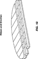
In einem spezifischen Ausführungsbeispiel stellt das vorliegende Verfahren ein zur Herstellung der vorliegenden Laserelemente geeignetes Ritzen bereit. Als Beispiel zeigt
Es wird nun auf
In einem bevorzugten Ausführungsbeispiel wird in dem Verfahren ein geeignetes Abscheidesystem verwendet, das zum Abscheiden auf jeder der Facetten ohne Verletzung des Vakuums konfiguriert ist. Das Abscheidesystem enthält eine Domstruktur mit ausreichender Höhe und räumlichem Volumen. Das System ermöglicht ein Umdrehen der in einer Spannvorrichtung konfigurierten Vielzahl von Stangen von einer Seite auf eine andere Seite und ein Exponieren der Rückfacette und der Frontfacette gemäß einem spezifischen Ausführungsbeispiel. In einem bevorzugten Ausführungsbeispiel ermöglicht das Verfahren ein erstes Abscheiden auf der Rückfacette, ein Rekonfigurieren der Stangenspannvorrichtung zum Exponieren der Vorderfacette und ein zweites Abscheiden auf der Vorderfacette ohne das Vakuum zu verletzen. In einem bevorzugten Ausführungsbeispiel ermöglicht das Verfahren ein Abscheiden von einer oder mehreren Schichten auf der Vorderseite und der Rückseite ohne Verletzen des Vakuums, um dadurch Zeit zu sparen und die Effizienz zu verbessern. In anderen Ausführungsbeispielen kann das Vakuum verletzt werden. Selbstverständlich sind andere Variationen, Abwandlungen und Alternativen möglich.In a preferred embodiment, the method uses a suitable deposition system that is configured to deposit on each of the facets without breaking the vacuum. The separation system contains a dome structure with sufficient height and volume. The system allows the plurality of rods configured in a jig to be turned over from one side to the other side and exposing the back facet and the front facet according to a specific embodiment. In a preferred embodiment, the method enables a first deposit on the back facet, a reconfiguration of the rod chuck to expose the front facet, and a second deposition on the front facet without breaking the vacuum. In a preferred embodiment, the method allows one or more layers to be deposited on the front and back without breaking the vacuum, thereby saving time and improving efficiency. In other embodiments, the vacuum may be violated. Of course, other variations, modifications and alternatives are possible.
Beispiel:Example:
Das Element weist einen Laserstreifenbereich auf, der über einem Abschnitt des nichtpolaren kristallinen Orientierungsoberflächenbereichs gebildet ist. Der Laserstreifenbereich ist gekennzeichnet durch eine Resonatororientierung, die im Wesentlichen parallel zur c-Richtung verläuft und ein erstes Ende und ein zweites Ende aufweist. Das Element weist eine erste gespaltene c-Flächen-Facette auf, die an dem ersten Ende des Laserstreifenbereichs vorgesehen ist, und eine zweite gespaltene c-Flächen-Facetten, die an dem zweiten Ende des Laserstreifenbereichs vorgesehen ist. Die erste gespaltene c-Facette ist im Wesentlichen parallel zur zweiten gespaltenen c-Facette. Spiegeloberflächen sind auf jeder der gespaltenen Oberflächen gebildet. Die erste gespaltene c-Facette umfasst eine erste Spiegeloberfläche. Die erste Spiegeloberfläche ist durch einen Ritz- und Brechvorgang gebildet, wie oben beschrieben wurde. Die erste Spiegeloberfläche umfasst eine reflektierende Beschichtung, die aus Aluminiumoxid und Hafnia besteht. Die zweite gespaltene c-Facette umfasst eine zweite Spiegeloberfläche. Die zweite Spiegeloberfläche wird durch einen Ritz- und Brechvorgang bereitgestellt, wie der hier bereits Beschriebene. Die zweite Spiegeloberfläche umfasst eine reflektierende Beschichtung, wie beispielsweise Siliziumdioxid und Hafnia. In einem spezifischen Ausführungsbeispiel weist der Laserstreifen eine Länge und Breite auf. Die Länge beträgt 400 bis 1000 μm und die Breite beträgt 1,4 bis 4 μm. Die Breite ist in ihren Abmessungen im Wesentlichen konstant.The element has a laser stripe region formed over a portion of the nonpolar crystalline orientation surface region. The laser stripe region is characterized by a resonator orientation that is substantially parallel to the c direction and has a first end and a second end. The element has a first split c-face facet provided at the first end of the laser stripe region and a second split c-face facet provided at the second end of the laser stripe region. The first split c-facet is substantially parallel to the second split c-facet. Mirror surfaces are formed on each of the cleaved surfaces. The first split c-facet comprises a first mirror surface. The first mirror surface is formed by a scribing and breaking operation, as described above. The first mirror surface comprises a reflective coating consisting of alumina and hafnia. The second split c-facet comprises a second mirror surface. The second mirror surface is provided by a scribing and breaking operation, as already described herein. The second mirror surface comprises a reflective coating, such as silicon dioxide and hafnia. In a specific embodiment, the laser strip has a length and width. The length is 400 to 1000 microns and the width is 1.4 to 4 microns. The width is essentially constant in its dimensions.
Wie gezeigt, ist das Element dadurch gekennzeichnet, dass ein spontan imitiertes Licht im Wesentlichen senkrecht zur c-Richtung polarisiert ist. Das heißt, das Element wirkt wie ein Laser. Das spontan emittierte Licht ist gekennzeichnet durch ein Polarisationsverhältnis senkrecht zur c-Richtung. Wie ebenfalls gezeigt wurde, ist das spontan imitierte Licht gekennzeichnet durch eine Wellenlänge von ungefähr 405 nm, um eine blau-violette Emission zu erreichen. Weitere enthaltene Parameter:
LeistungCW > 350 mW;
Ith < 35 mA;
SE > 1,0 W/A; und
Gepackt auf einen TO-56-Kopf.As shown, the element is characterized in that a spontaneously imitated light is polarized substantially perpendicular to the c direction. That is, the element acts like a laser. The spontaneously emitted light is characterized by a polarization ratio perpendicular to the c-direction. As also shown, the spontaneously imitated light is characterized by a wavelength of about 405 nm to achieve blue-violet emission. Other included parameters:
Power CW > 350 mW;
I th <35 mA;
SE> 1.0 W / A; and
Packed on a TO-56 head.
Wie gezeigt, ist in der Graphik ein Leistungs- und Stromverhältnis für das betreffende Laserelement bei ungefähr 25° Celsius dargestellt. Darüberhinaus ist die Wellenlänge für das betreffende Laserelement mit ungefähr 405 nm angegeben. Wiederum handelt es sich bei dem vorliegenden Element lediglich um eine Erläuterung und der Umfang der vorliegenden Ansprüche sollte nicht unangemessen eingeschränkt werden. Ein Fachmann würde andere Variationen, Abwandlungen und Alternativen erkennen.As shown, the graph shows a power and current ratio for the particular laser element at about 25 ° Celsius. In addition, the wavelength for the laser element in question is given as approximately 405 nm. Again, the present element is merely illustrative and the scope of the present claims should not be unduly limited. A person skilled in the art would recognize other variations, modifications and alternatives.
In anderen Ausführungsbeispielen umfasst die vorliegende Erfindung ein Element und ein Verfahren, die auf anderen, Gallium und Stickstoff enthaltenen Substratorientierungen aufgebaut sind. In einem spezifischen Ausführungsbeispiel ist das Gallium und Stickstoff enthaltende Substrat auf einer Ebenenfamilie mit einer {20-21}-Kristallorientierung aufgebaut. In einem spezifischen Ausführungsbeispiel ist {20-21} um 14,9° von der m-Ebene in Richtung der c-Ebene (0001) versetzt. Als Beispiel beträgt der Fehlschnitt oder Verschnitt +/–17° von der m-Ebene in Richtung der c-Ebene oder alternativ ungefähr an der {20-21}-Kristallorientierungsebene. Als weiteres Beispiel enthält das vorliegende Element einen in einer Projektion der c-Richtung orientierten Laserstreifen, der senkrecht zu der a-Richtung verläuft (oder alternativ auf der m-Ebene, wo er in der c-Richtung konfiguriert ist). In einem oder mehreren Ausführungsbeispielen wäre die gespaltene Facette die Gallium und Stickstoff enthaltende Fläche (z. B. GaN-Fläche), das heißt, +/–5° von einer Richtung senkrecht zur Projektion der c-Richtung (oder alternativ, für den m-Ebenen-Laser, handelt es sich um die c-Fläche). Selbstverständlich sind andere Variationen, Abwandlungen und Alternativen möglich.In other embodiments, the present invention includes an element and method constructed on other substrate orientations containing gallium and nitrogen. In a specific embodiment, the gallium and nitrogen containing substrate is built on a {20-21} crystal orientation plane family. In a specific embodiment, {20-21} is offset by 14.9 degrees from the m-plane toward the c-plane (0001). For example, the miscut or blend is +/- 17 ° from the m-plane in the direction of the c-plane, or alternatively approximately at the {20-21} crystal orientation plane. As another example, the present element includes a laser stripe oriented in a projection of the c-direction that is perpendicular to the a-direction (or alternatively on the m-plane where it is configured in the c-direction). In one or more embodiments, the cleaved facet would be the gallium and nitrogen containing surface (eg, GaN surface), that is, +/- 5 ° from a direction perpendicular to the c direction projection (or alternatively, for the m Level laser, it is the c-area). Of course, other variations, modifications and alternatives are possible.
Während oben eine vollständige Beschreibung der spezifischen Ausführungsbeispiele angegeben wurde, können verschiedene Abwandlungen, alternative Konstruktionen und Äquivalente verwendet werden. Daher sollten die vorstehende Beschreibung und Erläuterungen nicht als Einschränkung des in den beigefügten Ansprüchen definierten Umfangs der vorliegenden Erfindung betrachtet werden.While a complete description of the specific embodiments has been presented above, various modifications, alternative constructions, and equivalents may be used. Therefore, the foregoing description and explanations should not be taken as limiting the scope of the present invention as defined in the appended claims.
Claims (34)
Applications Claiming Priority (5)
| Application Number | Priority Date | Filing Date | Title |
|---|---|---|---|
| US16892609P | 2009-04-13 | 2009-04-13 | |
| US61/168,926 | 2009-04-13 | ||
| US24350209P | 2009-09-17 | 2009-09-17 | |
| US61/243,502 | 2009-09-17 | ||
| PCT/US2010/030939 WO2010120819A1 (en) | 2009-04-13 | 2010-04-13 | Optical device structure using gan substrates for laser applications |
Publications (1)
| Publication Number | Publication Date |
|---|---|
| DE112010001615T5 true DE112010001615T5 (en) | 2012-08-02 |
Family
ID=42982821
Family Applications (1)
| Application Number | Title | Priority Date | Filing Date |
|---|---|---|---|
| DE112010001615T Ceased DE112010001615T5 (en) | 2009-04-13 | 2010-04-13 | Structure of an optical element using GaN substrates for laser applications |
Country Status (5)
| Country | Link |
|---|---|
| US (1) | US9531164B2 (en) |
| JP (1) | JP5780605B2 (en) |
| CN (1) | CN102396083B (en) |
| DE (1) | DE112010001615T5 (en) |
| WO (1) | WO2010120819A1 (en) |
Families Citing this family (92)
| Publication number | Priority date | Publication date | Assignee | Title |
|---|---|---|---|---|
| US8847249B2 (en) | 2008-06-16 | 2014-09-30 | Soraa, Inc. | Solid-state optical device having enhanced indium content in active regions |
| US20100006873A1 (en) * | 2008-06-25 | 2010-01-14 | Soraa, Inc. | HIGHLY POLARIZED WHITE LIGHT SOURCE BY COMBINING BLUE LED ON SEMIPOLAR OR NONPOLAR GaN WITH YELLOW LED ON SEMIPOLAR OR NONPOLAR GaN |
| US8143148B1 (en) | 2008-07-14 | 2012-03-27 | Soraa, Inc. | Self-aligned multi-dielectric-layer lift off process for laser diode stripes |
| US8259769B1 (en) | 2008-07-14 | 2012-09-04 | Soraa, Inc. | Integrated total internal reflectors for high-gain laser diodes with high quality cleaved facets on nonpolar/semipolar GaN substrates |
| US8805134B1 (en) | 2012-02-17 | 2014-08-12 | Soraa Laser Diode, Inc. | Methods and apparatus for photonic integration in non-polar and semi-polar oriented wave-guided optical devices |
| WO2010017148A1 (en) | 2008-08-04 | 2010-02-11 | Soraa, Inc. | White light devices using non-polar or semipolar gallium containing materials and phosphors |
| US8284810B1 (en) | 2008-08-04 | 2012-10-09 | Soraa, Inc. | Solid state laser device using a selected crystal orientation in non-polar or semi-polar GaN containing materials and methods |
| US8247886B1 (en) | 2009-03-09 | 2012-08-21 | Soraa, Inc. | Polarization direction of optical devices using selected spatial configurations |
| US8252662B1 (en) | 2009-03-28 | 2012-08-28 | Soraa, Inc. | Method and structure for manufacture of light emitting diode devices using bulk GaN |
| US8422525B1 (en) * | 2009-03-28 | 2013-04-16 | Soraa, Inc. | Optical device structure using miscut GaN substrates for laser applications |
| US8254425B1 (en) | 2009-04-17 | 2012-08-28 | Soraa, Inc. | Optical device structure using GaN substrates and growth structures for laser applications |
| DE112010001615T5 (en) | 2009-04-13 | 2012-08-02 | Soraa, Inc. | Structure of an optical element using GaN substrates for laser applications |
| US8837545B2 (en) | 2009-04-13 | 2014-09-16 | Soraa Laser Diode, Inc. | Optical device structure using GaN substrates and growth structures for laser applications |
| US8294179B1 (en) | 2009-04-17 | 2012-10-23 | Soraa, Inc. | Optical device structure using GaN substrates and growth structures for laser applications |
| US8634442B1 (en) | 2009-04-13 | 2014-01-21 | Soraa Laser Diode, Inc. | Optical device structure using GaN substrates for laser applications |
| US8242522B1 (en) | 2009-05-12 | 2012-08-14 | Soraa, Inc. | Optical device structure using non-polar GaN substrates and growth structures for laser applications in 481 nm |
| US8416825B1 (en) | 2009-04-17 | 2013-04-09 | Soraa, Inc. | Optical device structure using GaN substrates and growth structure for laser applications |
| US9829780B2 (en) | 2009-05-29 | 2017-11-28 | Soraa Laser Diode, Inc. | Laser light source for a vehicle |
| US10108079B2 (en) | 2009-05-29 | 2018-10-23 | Soraa Laser Diode, Inc. | Laser light source for a vehicle |
| US8247887B1 (en) | 2009-05-29 | 2012-08-21 | Soraa, Inc. | Method and surface morphology of non-polar gallium nitride containing substrates |
| US8427590B2 (en) | 2009-05-29 | 2013-04-23 | Soraa, Inc. | Laser based display method and system |
| US8509275B1 (en) | 2009-05-29 | 2013-08-13 | Soraa, Inc. | Gallium nitride based laser dazzling device and method |
| US9800017B1 (en) | 2009-05-29 | 2017-10-24 | Soraa Laser Diode, Inc. | Laser device and method for a vehicle |
| US9250044B1 (en) | 2009-05-29 | 2016-02-02 | Soraa Laser Diode, Inc. | Gallium and nitrogen containing laser diode dazzling devices and methods of use |
| US8384300B2 (en) | 2009-09-01 | 2013-02-26 | Topanga Technologies, Inc. | Integrated RF electrodeless plasma lamp device and methods |
| US8314429B1 (en) | 2009-09-14 | 2012-11-20 | Soraa, Inc. | Multi color active regions for white light emitting diode |
| US8750342B1 (en) | 2011-09-09 | 2014-06-10 | Soraa Laser Diode, Inc. | Laser diodes with scribe structures |
| US8355418B2 (en) | 2009-09-17 | 2013-01-15 | Soraa, Inc. | Growth structures and method for forming laser diodes on {20-21} or off cut gallium and nitrogen containing substrates |
| US8933644B2 (en) | 2009-09-18 | 2015-01-13 | Soraa, Inc. | LED lamps with improved quality of light |
| US9583678B2 (en) | 2009-09-18 | 2017-02-28 | Soraa, Inc. | High-performance LED fabrication |
| US9293644B2 (en) | 2009-09-18 | 2016-03-22 | Soraa, Inc. | Power light emitting diode and method with uniform current density operation |
| DE112010003700T5 (en) | 2009-09-18 | 2013-02-28 | Soraa, Inc. | POWER LIGHT DIODE AND METHOD WITH POWER DENSITY OPERATION |
| US10147850B1 (en) | 2010-02-03 | 2018-12-04 | Soraa, Inc. | System and method for providing color light sources in proximity to predetermined wavelength conversion structures |
| US8905588B2 (en) | 2010-02-03 | 2014-12-09 | Sorra, Inc. | System and method for providing color light sources in proximity to predetermined wavelength conversion structures |
| JP5972798B2 (en) * | 2010-03-04 | 2016-08-17 | ザ リージェンツ オブ ザ ユニバーシティ オブ カリフォルニア | Semipolar III-nitride optoelectronic device on M-plane substrate with miscut less than +/− 15 degrees in C direction |
| US9927611B2 (en) | 2010-03-29 | 2018-03-27 | Soraa Laser Diode, Inc. | Wearable laser based display method and system |
| US8451876B1 (en) | 2010-05-17 | 2013-05-28 | Soraa, Inc. | Method and system for providing bidirectional light sources with broad spectrum |
| US9450143B2 (en) | 2010-06-18 | 2016-09-20 | Soraa, Inc. | Gallium and nitrogen containing triangular or diamond-shaped configuration for optical devices |
| US8816319B1 (en) * | 2010-11-05 | 2014-08-26 | Soraa Laser Diode, Inc. | Method of strain engineering and related optical device using a gallium and nitrogen containing active region |
| US8975615B2 (en) * | 2010-11-09 | 2015-03-10 | Soraa Laser Diode, Inc. | Method of fabricating optical devices using laser treatment of contact regions of gallium and nitrogen containing material |
| US9048170B2 (en) | 2010-11-09 | 2015-06-02 | Soraa Laser Diode, Inc. | Method of fabricating optical devices using laser treatment |
| GB2487531A (en) * | 2011-01-20 | 2012-08-01 | Sharp Kk | Substrate system consisting of a metamorphic transition region comprising a laminate of AlxGa1-x N and the same material as the substrate. |
| US9025635B2 (en) | 2011-01-24 | 2015-05-05 | Soraa Laser Diode, Inc. | Laser package having multiple emitters configured on a support member |
| US9595813B2 (en) * | 2011-01-24 | 2017-03-14 | Soraa Laser Diode, Inc. | Laser package having multiple emitters configured on a substrate member |
| US9318875B1 (en) | 2011-01-24 | 2016-04-19 | Soraa Laser Diode, Inc. | Color converting element for laser diode |
| JP5553035B2 (en) * | 2011-01-24 | 2014-07-16 | 住友電気工業株式会社 | Gallium nitride semiconductor laser device |
| US9093820B1 (en) | 2011-01-25 | 2015-07-28 | Soraa Laser Diode, Inc. | Method and structure for laser devices using optical blocking regions |
| US9287684B2 (en) | 2011-04-04 | 2016-03-15 | Soraa Laser Diode, Inc. | Laser package having multiple emitters with color wheel |
| JP5716524B2 (en) * | 2011-05-06 | 2015-05-13 | 日亜化学工業株式会社 | Method for manufacturing light emitting device |
| US8686431B2 (en) | 2011-08-22 | 2014-04-01 | Soraa, Inc. | Gallium and nitrogen containing trilateral configuration for optical devices |
| US8971370B1 (en) | 2011-10-13 | 2015-03-03 | Soraa Laser Diode, Inc. | Laser devices using a semipolar plane |
| CN102522318B (en) * | 2011-12-30 | 2013-11-27 | 厦门大学 | Self-split transfer method of GaN-based epitaxial thin film |
| US9020003B1 (en) | 2012-03-14 | 2015-04-28 | Soraa Laser Diode, Inc. | Group III-nitride laser diode grown on a semi-polar orientation of gallium and nitrogen containing substrates |
| US9343871B1 (en) | 2012-04-05 | 2016-05-17 | Soraa Laser Diode, Inc. | Facet on a gallium and nitrogen containing laser diode |
| US9800016B1 (en) | 2012-04-05 | 2017-10-24 | Soraa Laser Diode, Inc. | Facet on a gallium and nitrogen containing laser diode |
| US10559939B1 (en) | 2012-04-05 | 2020-02-11 | Soraa Laser Diode, Inc. | Facet on a gallium and nitrogen containing laser diode |
| US9099843B1 (en) | 2012-07-19 | 2015-08-04 | Soraa Laser Diode, Inc. | High operating temperature laser diodes |
| US8971368B1 (en) | 2012-08-16 | 2015-03-03 | Soraa Laser Diode, Inc. | Laser devices having a gallium and nitrogen containing semipolar surface orientation |
| US9184563B1 (en) | 2012-08-30 | 2015-11-10 | Soraa Laser Diode, Inc. | Laser diodes with an etched facet and surface treatment |
| US9978904B2 (en) | 2012-10-16 | 2018-05-22 | Soraa, Inc. | Indium gallium nitride light emitting devices |
| US9166372B1 (en) | 2013-06-28 | 2015-10-20 | Soraa Laser Diode, Inc. | Gallium nitride containing laser device configured on a patterned substrate |
| US9379525B2 (en) | 2014-02-10 | 2016-06-28 | Soraa Laser Diode, Inc. | Manufacturable laser diode |
| US9520695B2 (en) | 2013-10-18 | 2016-12-13 | Soraa Laser Diode, Inc. | Gallium and nitrogen containing laser device having confinement region |
| US9362715B2 (en) | 2014-02-10 | 2016-06-07 | Soraa Laser Diode, Inc | Method for manufacturing gallium and nitrogen bearing laser devices with improved usage of substrate material |
| US9368939B2 (en) | 2013-10-18 | 2016-06-14 | Soraa Laser Diode, Inc. | Manufacturable laser diode formed on C-plane gallium and nitrogen material |
| US9419189B1 (en) | 2013-11-04 | 2016-08-16 | Soraa, Inc. | Small LED source with high brightness and high efficiency |
| US9209596B1 (en) | 2014-02-07 | 2015-12-08 | Soraa Laser Diode, Inc. | Manufacturing a laser diode device from a plurality of gallium and nitrogen containing substrates |
| US9520697B2 (en) | 2014-02-10 | 2016-12-13 | Soraa Laser Diode, Inc. | Manufacturable multi-emitter laser diode |
| US9871350B2 (en) | 2014-02-10 | 2018-01-16 | Soraa Laser Diode, Inc. | Manufacturable RGB laser diode source |
| US9564736B1 (en) | 2014-06-26 | 2017-02-07 | Soraa Laser Diode, Inc. | Epitaxial growth of p-type cladding regions using nitrogen gas for a gallium and nitrogen containing laser diode |
| US12126143B2 (en) | 2014-11-06 | 2024-10-22 | Kyocera Sld Laser, Inc. | Method of manufacture for an ultraviolet emitting optoelectronic device |
| US9246311B1 (en) | 2014-11-06 | 2016-01-26 | Soraa Laser Diode, Inc. | Method of manufacture for an ultraviolet laser diode |
| US9666677B1 (en) | 2014-12-23 | 2017-05-30 | Soraa Laser Diode, Inc. | Manufacturable thin film gallium and nitrogen containing devices |
| US9653642B1 (en) | 2014-12-23 | 2017-05-16 | Soraa Laser Diode, Inc. | Manufacturable RGB display based on thin film gallium and nitrogen containing light emitting diodes |
| US10938182B2 (en) | 2015-08-19 | 2021-03-02 | Soraa Laser Diode, Inc. | Specialized integrated light source using a laser diode |
| US11437774B2 (en) | 2015-08-19 | 2022-09-06 | Kyocera Sld Laser, Inc. | High-luminous flux laser-based white light source |
| US10879673B2 (en) | 2015-08-19 | 2020-12-29 | Soraa Laser Diode, Inc. | Integrated white light source using a laser diode and a phosphor in a surface mount device package |
| US11437775B2 (en) | 2015-08-19 | 2022-09-06 | Kyocera Sld Laser, Inc. | Integrated light source using a laser diode |
| US9787963B2 (en) | 2015-10-08 | 2017-10-10 | Soraa Laser Diode, Inc. | Laser lighting having selective resolution |
| US20170338625A1 (en) * | 2016-05-20 | 2017-11-23 | Macom Technology Solutions Holdings, Inc. | Semiconductor lasers and processes for the planarization of semiconductor lasers |
| US10771155B2 (en) | 2017-09-28 | 2020-09-08 | Soraa Laser Diode, Inc. | Intelligent visible light with a gallium and nitrogen containing laser source |
| US10222474B1 (en) | 2017-12-13 | 2019-03-05 | Soraa Laser Diode, Inc. | Lidar systems including a gallium and nitrogen containing laser light source |
| US10551728B1 (en) | 2018-04-10 | 2020-02-04 | Soraa Laser Diode, Inc. | Structured phosphors for dynamic lighting |
| US11421843B2 (en) | 2018-12-21 | 2022-08-23 | Kyocera Sld Laser, Inc. | Fiber-delivered laser-induced dynamic light system |
| US11239637B2 (en) | 2018-12-21 | 2022-02-01 | Kyocera Sld Laser, Inc. | Fiber delivered laser induced white light system |
| US11884202B2 (en) | 2019-01-18 | 2024-01-30 | Kyocera Sld Laser, Inc. | Laser-based fiber-coupled white light system |
| US12152742B2 (en) | 2019-01-18 | 2024-11-26 | Kyocera Sld Laser, Inc. | Laser-based light guide-coupled wide-spectrum light system |
| US12000552B2 (en) | 2019-01-18 | 2024-06-04 | Kyocera Sld Laser, Inc. | Laser-based fiber-coupled white light system for a vehicle |
| US11228158B2 (en) | 2019-05-14 | 2022-01-18 | Kyocera Sld Laser, Inc. | Manufacturable laser diodes on a large area gallium and nitrogen containing substrate |
| US10903623B2 (en) | 2019-05-14 | 2021-01-26 | Soraa Laser Diode, Inc. | Method and structure for manufacturable large area gallium and nitrogen containing substrate |
| US12191626B1 (en) | 2020-07-31 | 2025-01-07 | Kyocera Sld Laser, Inc. | Vertically emitting laser devices and chip-scale-package laser devices and laser-based, white light emitting devices |
| KR20220149828A (en) | 2021-04-30 | 2022-11-09 | 삼성전자주식회사 | Semiconductor devices |
Family Cites Families (254)
| Publication number | Priority date | Publication date | Assignee | Title |
|---|---|---|---|---|
| US6153010A (en) | 1997-04-11 | 2000-11-28 | Nichia Chemical Industries Ltd. | Method of growing nitride semiconductors, nitride semiconductor substrate and nitride semiconductor device |
| US4341592A (en) | 1975-08-04 | 1982-07-27 | Texas Instruments Incorporated | Method for removing photoresist layer from substrate by ozone treatment |
| US4318058A (en) | 1979-04-24 | 1982-03-02 | Nippon Electric Co., Ltd. | Semiconductor diode laser array |
| FR2596070A1 (en) | 1986-03-21 | 1987-09-25 | Labo Electronique Physique | DEVICE COMPRISING A PLANAR SUSCEPTOR ROTATING PARALLEL TO A REFERENCE PLANE AROUND A PERPENDICULAR AXIS AT THIS PLAN |
| US4911102A (en) | 1987-01-31 | 1990-03-27 | Toyoda Gosei Co., Ltd. | Process of vapor growth of gallium nitride and its apparatus |
| JPH03287770A (en) | 1990-04-05 | 1991-12-18 | Hitachi Electron Eng Co Ltd | Single wafer processing atmospheric cvd device |
| US5334277A (en) | 1990-10-25 | 1994-08-02 | Nichia Kagaky Kogyo K.K. | Method of vapor-growing semiconductor crystal and apparatus for vapor-growing the same |
| US5157466A (en) | 1991-03-19 | 1992-10-20 | Conductus, Inc. | Grain boundary junctions in high temperature superconductor films |
| JP3148004B2 (en) | 1992-07-06 | 2001-03-19 | 株式会社東芝 | Optical CVD apparatus and method for manufacturing semiconductor device using the same |
| US5578839A (en) | 1992-11-20 | 1996-11-26 | Nichia Chemical Industries, Ltd. | Light-emitting gallium nitride-based compound semiconductor device |
| US5331654A (en) | 1993-03-05 | 1994-07-19 | Photonics Research Incorporated | Polarized surface-emitting laser |
| JPH06267846A (en) | 1993-03-10 | 1994-09-22 | Canon Inc | Diamond electronic device and its manufacturing method |
| US5647945A (en) | 1993-08-25 | 1997-07-15 | Tokyo Electron Limited | Vacuum processing apparatus |
| JP3623001B2 (en) | 1994-02-25 | 2005-02-23 | 住友電気工業株式会社 | Method for forming single crystalline thin film |
| JPH07254732A (en) | 1994-03-15 | 1995-10-03 | Toshiba Corp | Semiconductor light emitting device |
| US5821555A (en) | 1995-03-27 | 1998-10-13 | Kabushiki Kaisha Toshiba | Semicoductor device having a hetero interface with a lowered barrier |
| US6072197A (en) | 1996-02-23 | 2000-06-06 | Fujitsu Limited | Semiconductor light emitting device with an active layer made of semiconductor having uniaxial anisotropy |
| JP3360265B2 (en) | 1996-04-26 | 2002-12-24 | 東京エレクトロン株式会社 | Plasma processing method and plasma processing apparatus |
| TW393521B (en) | 1996-05-23 | 2000-06-11 | Ebara Corp | Vaporizer apparatus and film deposition apparatus therewith |
| US6183565B1 (en) | 1997-07-08 | 2001-02-06 | Asm International N.V | Method and apparatus for supporting a semiconductor wafer during processing |
| US6542526B1 (en) | 1996-10-30 | 2003-04-01 | Hitachi, Ltd. | Optical information processor and semiconductor light emitting device suitable for the same |
| US5760484A (en) * | 1997-02-11 | 1998-06-02 | Mosel Vitelic Inc. | Alignment mark pattern for semiconductor process |
| KR100447367B1 (en) | 1997-03-07 | 2004-09-08 | 샤프 가부시키가이샤 | Gallium nitride semiconductor light emitting element with active layer having multiplex quantum well structure and semiconductor laser light source device |
| US6069394A (en) | 1997-04-09 | 2000-05-30 | Matsushita Electronics Corporation | Semiconductor substrate, semiconductor device and method of manufacturing the same |
| US5926493A (en) | 1997-05-20 | 1999-07-20 | Sdl, Inc. | Optical semiconductor device with diffraction grating structure |
| JPH10335750A (en) | 1997-06-03 | 1998-12-18 | Sony Corp | Semiconductor substrate and semiconductor device |
| JP3653169B2 (en) | 1998-01-26 | 2005-05-25 | シャープ株式会社 | Gallium nitride semiconductor laser device |
| US6147953A (en) | 1998-03-25 | 2000-11-14 | Duncan Technologies, Inc. | Optical signal transmission apparatus |
| US6195381B1 (en) | 1998-04-27 | 2001-02-27 | Wisconsin Alumni Research Foundation | Narrow spectral width high-power distributed feedback semiconductor lasers |
| US6108937A (en) | 1998-09-10 | 2000-08-29 | Asm America, Inc. | Method of cooling wafers |
| JP2000138168A (en) | 1998-10-29 | 2000-05-16 | Shin Etsu Handotai Co Ltd | Semiconductor wafer and vapor phase growth equipment |
| JP2000209705A (en) | 1999-01-13 | 2000-07-28 | Shinko Electric Co Ltd | Automatic guided vehicle system |
| US6711191B1 (en) | 1999-03-04 | 2004-03-23 | Nichia Corporation | Nitride semiconductor laser device |
| US6239454B1 (en) | 1999-05-10 | 2001-05-29 | Lucent Technologies Inc. | Net strain reduction in integrated laser-modulator |
| DE60033829T2 (en) | 1999-09-07 | 2007-10-11 | Sixon Inc. | SiC SEMICONDUCTOR SHEET, SiC SEMICONDUCTOR ELEMENT AND MANUFACTURING METHOD FOR A SiC SEMICONDUCTOR DISC |
| US6451157B1 (en) | 1999-09-23 | 2002-09-17 | Lam Research Corporation | Gas distribution apparatus for semiconductor processing |
| TW580735B (en) | 2000-02-21 | 2004-03-21 | Hitachi Ltd | Plasma treatment apparatus and treating method of sample material |
| AU2001247240A1 (en) | 2000-03-01 | 2001-09-12 | Heraeus Amersil, Inc. | Method, apparatus, and article of manufacture for determining an amount of energy needed to bring a quartz workpiece to a fusion weldable condition |
| TW518767B (en) | 2000-03-31 | 2003-01-21 | Toyoda Gosei Kk | Production method of III nitride compound semiconductor and III nitride compound semiconductor element |
| US6554905B1 (en) | 2000-04-17 | 2003-04-29 | Asm America, Inc. | Rotating semiconductor processing apparatus |
| US6423565B1 (en) | 2000-05-30 | 2002-07-23 | Kurt L. Barth | Apparatus and processes for the massproduction of photovotaic modules |
| EP1306944B1 (en) * | 2000-06-08 | 2007-07-04 | Nichia Corporation | Semiconductor laser device, and method of manufacturing the same |
| US7043129B2 (en) | 2000-06-16 | 2006-05-09 | Wayne State University | Wide bandgap semiconductor waveguide structures |
| US6586762B2 (en) | 2000-07-07 | 2003-07-01 | Nichia Corporation | Nitride semiconductor device with improved lifetime and high output power |
| US6680959B2 (en) | 2000-07-18 | 2004-01-20 | Rohm Co., Ltd. | Semiconductor light emitting device and semiconductor laser |
| AU2001288225A1 (en) | 2000-07-24 | 2002-02-05 | The University Of Maryland College Park | Spatially programmable microelectronics process equipment using segmented gas injection showerhead with exhaust gas recirculation |
| US6858882B2 (en) | 2000-09-08 | 2005-02-22 | Sharp Kabushiki Kaisha | Nitride semiconductor light-emitting device and optical device including the same |
| US7053413B2 (en) | 2000-10-23 | 2006-05-30 | General Electric Company | Homoepitaxial gallium-nitride-based light emitting device and method for producing |
| JP2002190635A (en) | 2000-12-20 | 2002-07-05 | Sharp Corp | Semiconductor laser device and method of manufacturing the same |
| US6489636B1 (en) | 2001-03-29 | 2002-12-03 | Lumileds Lighting U.S., Llc | Indium gallium nitride smoothing structures for III-nitride devices |
| US6635904B2 (en) | 2001-03-29 | 2003-10-21 | Lumileds Lighting U.S., Llc | Indium gallium nitride smoothing structures for III-nitride devices |
| US6939730B2 (en) | 2001-04-24 | 2005-09-06 | Sony Corporation | Nitride semiconductor, semiconductor device, and method of manufacturing the same |
| US6734530B2 (en) | 2001-06-06 | 2004-05-11 | Matsushita Electric Industries Co., Ltd. | GaN-based compound semiconductor EPI-wafer and semiconductor element using the same |
| WO2002103866A1 (en) | 2001-06-15 | 2002-12-27 | Nichia Corporation | Semiconductor laser element, and its manufacturing method |
| JP3639807B2 (en) | 2001-06-27 | 2005-04-20 | キヤノン株式会社 | Optical element and manufacturing method |
| US6379985B1 (en) * | 2001-08-01 | 2002-04-30 | Xerox Corporation | Methods for cleaving facets in III-V nitrides grown on c-face sapphire substrates |
| JP3749243B2 (en) | 2001-09-03 | 2006-02-22 | 松下電器産業株式会社 | Semiconductor light emitting device, light emitting apparatus, and method for manufacturing semiconductor light emitting device |
| JP3785970B2 (en) | 2001-09-03 | 2006-06-14 | 日本電気株式会社 | Method for manufacturing group III nitride semiconductor device |
| US7303630B2 (en) | 2003-11-05 | 2007-12-04 | Sumitomo Electric Industries, Ltd. | Method of growing GaN crystal, method of producing single crystal GaN substrate, and single crystal GaN substrate |
| JP3801125B2 (en) | 2001-10-09 | 2006-07-26 | 住友電気工業株式会社 | Single crystal gallium nitride substrate, method for crystal growth of single crystal gallium nitride, and method for manufacturing single crystal gallium nitride substrate |
| CA2462102A1 (en) | 2001-09-29 | 2003-04-10 | Cree, Inc. | Apparatus for inverted cvd |
| US6833564B2 (en) | 2001-11-02 | 2004-12-21 | Lumileds Lighting U.S., Llc | Indium gallium nitride separate confinement heterostructure light emitting devices |
| US8545629B2 (en) | 2001-12-24 | 2013-10-01 | Crystal Is, Inc. | Method and apparatus for producing large, single-crystals of aluminum nitride |
| US6977780B2 (en) | 2001-12-27 | 2005-12-20 | Fuji Photo Film Co., Ltd. | Image exposure device and laser exposure device applied thereto |
| WO2003058726A1 (en) | 2001-12-28 | 2003-07-17 | Sanken Electric Co., Ltd. | Semiconductor light-emitting device, light-emitting display, method for manufacturing semiconductor light-emitting device, and method for manufacturing light-emitting display |
| JP2003218034A (en) | 2002-01-17 | 2003-07-31 | Sony Corp | Selective growth method, semiconductor light emitting device and method of manufacturing the same |
| JP3898537B2 (en) | 2002-03-19 | 2007-03-28 | 日本電信電話株式会社 | Nitride semiconductor thin film forming method and nitride semiconductor light emitting device |
| US6891227B2 (en) | 2002-03-20 | 2005-05-10 | International Business Machines Corporation | Self-aligned nanotube field effect transistor and method of fabricating same |
| US7063741B2 (en) | 2002-03-27 | 2006-06-20 | General Electric Company | High pressure high temperature growth of crystalline group III metal nitrides |
| CN100439561C (en) | 2002-04-19 | 2008-12-03 | 马特森技术公司 | System for Depositing Films on Substrates Using Low Vapor Pressure Gas Precursors |
| US7008484B2 (en) | 2002-05-06 | 2006-03-07 | Applied Materials Inc. | Method and apparatus for deposition of low dielectric constant materials |
| US6927382B2 (en) | 2002-05-22 | 2005-08-09 | Agilent Technologies | Optical excitation/detection device and method for making same using fluidic self-assembly techniques |
| US6995032B2 (en) | 2002-07-19 | 2006-02-07 | Cree, Inc. | Trench cut light emitting diodes and methods of fabricating same |
| JP3861036B2 (en) | 2002-08-09 | 2006-12-20 | 三菱重工業株式会社 | Plasma CVD equipment |
| US6809781B2 (en) | 2002-09-24 | 2004-10-26 | General Electric Company | Phosphor blends and backlight sources for liquid crystal displays |
| US7009199B2 (en) | 2002-10-22 | 2006-03-07 | Cree, Inc. | Electronic devices having a header and antiparallel connected light emitting diodes for producing light from AC current |
| US7186302B2 (en) | 2002-12-16 | 2007-03-06 | The Regents Of The University Of California | Fabrication of nonpolar indium gallium nitride thin films, heterostructures and devices by metalorganic chemical vapor deposition |
| JP2004241570A (en) | 2003-02-05 | 2004-08-26 | Fujitsu Ltd | Semiconductor laser |
| US7068905B2 (en) | 2003-03-12 | 2006-06-27 | Daryoosh Vakhshoori | Extended optical bandwidth semiconductor source |
| CN1781195A (en) | 2003-03-18 | 2006-05-31 | 克利斯托光子学公司 | Method for making group III nitride devices and devices produced thereby |
| US7033858B2 (en) | 2003-03-18 | 2006-04-25 | Crystal Photonics, Incorporated | Method for making Group III nitride devices and devices produced thereby |
| JP2004304111A (en) | 2003-04-01 | 2004-10-28 | Sharp Corp | Multi-wavelength laser device |
| US7187185B2 (en) | 2004-09-29 | 2007-03-06 | Loadstar Sensors Inc | Area-change sensing through capacitive techniques |
| CN1538534A (en) | 2003-04-15 | 2004-10-20 | 郑荣彬 | White light illuminating device |
| US7118781B1 (en) | 2003-04-16 | 2006-10-10 | Cree, Inc. | Methods for controlling formation of deposits in a deposition system and deposition methods including the same |
| WO2004111297A1 (en) | 2003-06-10 | 2004-12-23 | Tokyo Electron Limited | Treatment gas supply mechanism, film-forming device, and film-forming method |
| JP4229005B2 (en) | 2003-06-26 | 2009-02-25 | 住友電気工業株式会社 | GaN substrate, method of manufacturing the same, and nitride semiconductor device |
| JP4011569B2 (en) | 2003-08-20 | 2007-11-21 | 株式会社東芝 | Semiconductor light emitting device |
| US7009215B2 (en) | 2003-10-24 | 2006-03-07 | General Electric Company | Group III-nitride based resonant cavity light emitting devices fabricated on single crystal gallium nitride substrates |
| US7128849B2 (en) | 2003-10-31 | 2006-10-31 | General Electric Company | Phosphors containing boron and metals of Group IIIA and IIIB |
| US7384481B2 (en) | 2003-12-29 | 2008-06-10 | Translucent Photonics, Inc. | Method of forming a rare-earth dielectric layer |
| JP4279698B2 (en) | 2004-01-30 | 2009-06-17 | シャープ株式会社 | LED element driving method and driving device, lighting device and display device |
| US20050285128A1 (en) | 2004-02-10 | 2005-12-29 | California Institute Of Technology | Surface plasmon light emitter structure and method of manufacture |
| JP4830315B2 (en) * | 2004-03-05 | 2011-12-07 | 日亜化学工業株式会社 | Semiconductor laser element |
| US20070242716A1 (en) | 2004-03-19 | 2007-10-18 | Arizona Board Of Regents, A Body Corporation Acting On Behalf Of Arizona State University | High Power Vcsels With Transverse Mode Control |
| US7408201B2 (en) | 2004-03-19 | 2008-08-05 | Philips Lumileds Lighting Company, Llc | Polarized semiconductor light emitting device |
| US8035113B2 (en) | 2004-04-15 | 2011-10-11 | The Trustees Of Boston University | Optical devices featuring textured semiconductor layers |
| US7061026B2 (en) | 2004-04-16 | 2006-06-13 | Arima Optoelectronics Corp. | High brightness gallium nitride-based light emitting diode with transparent conducting oxide spreading layer |
| DE102004021233A1 (en) | 2004-04-30 | 2005-12-01 | Osram Opto Semiconductors Gmbh | LED array |
| KR100718188B1 (en) | 2004-05-07 | 2007-05-15 | 삼성코닝 주식회사 | Non-polar single crystalline a-plane nitride semiconductor wafer and preparation thereof |
| EP1598681A3 (en) | 2004-05-17 | 2006-03-01 | Carl Zeiss SMT AG | Optical component with curved surface and multi-layer coating |
| US8227820B2 (en) | 2005-02-09 | 2012-07-24 | The Regents Of The University Of California | Semiconductor light-emitting device |
| US7858996B2 (en) | 2006-02-17 | 2010-12-28 | The Regents Of The University Of California | Method for growth of semipolar (Al,In,Ga,B)N optoelectronic devices |
| US7956360B2 (en) | 2004-06-03 | 2011-06-07 | The Regents Of The University Of California | Growth of planar reduced dislocation density M-plane gallium nitride by hydride vapor phase epitaxy |
| US20080092812A1 (en) | 2004-06-10 | 2008-04-24 | Mcdiarmid James | Methods and Apparatuses for Depositing Uniform Layers |
| US7019325B2 (en) | 2004-06-16 | 2006-03-28 | Exalos Ag | Broadband light emitting device |
| KR100541110B1 (en) | 2004-06-25 | 2006-01-11 | 삼성전기주식회사 | Multi-wavelength semiconductor laser manufacturing method |
| US7288679B2 (en) | 2004-08-06 | 2007-10-30 | Agfa-Gevaert | Device provided with a dedicated dye compound |
| JP4290095B2 (en) | 2004-08-16 | 2009-07-01 | キヤノン株式会社 | Display optical system and image display system |
| TWI241036B (en) | 2004-08-18 | 2005-10-01 | Formosa Epitaxy Inc | GaN LED structure with enhanced light emitting luminance |
| JP2006073076A (en) | 2004-09-01 | 2006-03-16 | Fujinon Corp | Object optical system for optical recording medium, and optical pickup device using the same |
| JP2006108435A (en) | 2004-10-06 | 2006-04-20 | Sumitomo Electric Ind Ltd | Nitride semiconductor wafer |
| KR100695419B1 (en) * | 2004-11-04 | 2007-03-15 | 주식회사 하이닉스반도체 | Internal power generator |
| US7858408B2 (en) | 2004-11-15 | 2010-12-28 | Koninklijke Philips Electronics N.V. | LED with phosphor tile and overmolded phosphor in lens |
| US7751455B2 (en) | 2004-12-14 | 2010-07-06 | Palo Alto Research Center Incorporated | Blue and green laser diodes with gallium nitride or indium gallium nitride cladding laser structure |
| US7564180B2 (en) | 2005-01-10 | 2009-07-21 | Cree, Inc. | Light emission device and method utilizing multiple emitters and multiple phosphors |
| US7358542B2 (en) | 2005-02-02 | 2008-04-15 | Lumination Llc | Red emitting phosphor materials for use in LED and LCD applications |
| US7932111B2 (en) | 2005-02-23 | 2011-04-26 | Cree, Inc. | Substrate removal process for high light extraction LEDs |
| JP2006270028A (en) | 2005-02-25 | 2006-10-05 | Mitsubishi Electric Corp | Semiconductor light emitting device |
| KR101145755B1 (en) | 2005-03-10 | 2012-05-16 | 재팬 사이언스 앤드 테크놀로지 에이젼시 | Technique for the growth of planar semi-polar gallium nitride |
| WO2006099211A2 (en) | 2005-03-11 | 2006-09-21 | Ponce Fernando A | Solid state light emitting device |
| EP1869526B1 (en) | 2005-03-30 | 2019-11-06 | Necsel Intellectual Property, Inc. | Manufacturable vertical extended cavity surface emitting laser arrays |
| US7483466B2 (en) | 2005-04-28 | 2009-01-27 | Canon Kabushiki Kaisha | Vertical cavity surface emitting laser device |
| KR100704492B1 (en) | 2005-05-02 | 2007-04-09 | 한국화학연구원 | Method for manufacturing white light emitting diode using phosphor |
| US7574791B2 (en) | 2005-05-10 | 2009-08-18 | Hitachi Global Storage Technologies Netherlands B.V. | Method to fabricate side shields for a magnetic sensor |
| US7358543B2 (en) | 2005-05-27 | 2008-04-15 | Avago Technologies Ecbu Ip (Singapore) Pte. Ltd. | Light emitting device having a layer of photonic crystals and a region of diffusing material and method for fabricating the device |
| TWI377602B (en) | 2005-05-31 | 2012-11-21 | Japan Science & Tech Agency | Growth of planar non-polar {1-100} m-plane gallium nitride with metalorganic chemical vapor deposition (mocvd) |
| TWI455181B (en) | 2005-06-01 | 2014-10-01 | 美國加利福尼亞大學董事會 | Growth and manufacturing techniques for semi-polar (Ga, Al, In, B) N films, heterostructures and devices |
| US20060288928A1 (en) * | 2005-06-10 | 2006-12-28 | Chang-Beom Eom | Perovskite-based thin film structures on miscut semiconductor substrates |
| US8148713B2 (en) | 2008-04-04 | 2012-04-03 | The Regents Of The University Of California | Method for fabrication of semipolar (Al, In, Ga, B)N based light emitting diodes |
| US20100220262A1 (en) | 2008-08-05 | 2010-09-02 | The Regents Of The University Of California | Linearly polarized backlight source in conjunction with polarized phosphor emission screens for use in liquid crystal displays |
| US20070081857A1 (en) | 2005-10-07 | 2007-04-12 | Yoon Jung H | Four parts manhole enabling an easy install and height adjustment |
| US20070086916A1 (en) | 2005-10-14 | 2007-04-19 | General Electric Company | Faceted structure, article, sensor device, and method |
| JP4879563B2 (en) | 2005-11-16 | 2012-02-22 | パナソニック株式会社 | Group III nitride semiconductor light emitting device |
| DE102005055252A1 (en) | 2005-11-19 | 2007-05-24 | Aixtron Ag | CVD reactor with slide-mounted susceptor holder |
| US20070138505A1 (en) | 2005-12-12 | 2007-06-21 | Kyma Technologies, Inc. | Low defect group III nitride films useful for electronic and optoelectronic devices and methods for making the same |
| JP5191650B2 (en) | 2005-12-16 | 2013-05-08 | シャープ株式会社 | Nitride semiconductor light emitting device and method for manufacturing nitride semiconductor light emitting device |
| JP4534978B2 (en) | 2005-12-21 | 2010-09-01 | トヨタ自動車株式会社 | Semiconductor thin film manufacturing equipment |
| EP1965416A3 (en) | 2005-12-22 | 2009-04-29 | Freiberger Compound Materials GmbH | Free-Standing III-N layers or devices obtained by selective masking of III-N layers during III-N layer growth |
| JP5896442B2 (en) | 2006-01-20 | 2016-03-30 | 国立研究開発法人科学技術振興機構 | Group III nitride film growth method |
| US8044412B2 (en) | 2006-01-20 | 2011-10-25 | Taiwan Semiconductor Manufacturing Company, Ltd | Package for a light emitting element |
| CN101009347A (en) | 2006-01-27 | 2007-08-01 | 中国科学院物理研究所 | Non polarity A side nitride film growing on the silicon(102) substrate and its making method and use |
| JP4711838B2 (en) | 2006-01-27 | 2011-06-29 | 株式会社東芝 | Multi-wavelength semiconductor laser device |
| JP4660400B2 (en) | 2006-03-14 | 2011-03-30 | シャープ株式会社 | Manufacturing method of nitride semiconductor laser device |
| US7459380B2 (en) | 2006-05-05 | 2008-12-02 | Applied Materials, Inc. | Dislocation-specific dielectric mask deposition and lateral epitaxial overgrowth to reduce dislocation density of nitride films |
| US7480322B2 (en) | 2006-05-15 | 2009-01-20 | The Regents Of The University Of California | Electrically-pumped (Ga,In,Al)N vertical-cavity surface-emitting laser |
| KR101263934B1 (en) | 2006-05-23 | 2013-05-10 | 엘지디스플레이 주식회사 | Light emitting diode and method of manufacturing thesame |
| JP4819577B2 (en) | 2006-05-31 | 2011-11-24 | キヤノン株式会社 | Pattern transfer method and pattern transfer apparatus |
| US20090273005A1 (en) | 2006-07-24 | 2009-11-05 | Hung-Yi Lin | Opto-electronic package structure having silicon-substrate and method of forming the same |
| US20080029152A1 (en) | 2006-08-04 | 2008-02-07 | Erel Milshtein | Laser scribing apparatus, systems, and methods |
| WO2008021403A2 (en) | 2006-08-16 | 2008-02-21 | The Regents Of The University Of California | Method for deposition of magnesium doped (al, in, ga, b)n layers |
| US7374960B1 (en) | 2006-08-23 | 2008-05-20 | Applied Materials, Inc. | Stress measurement and stress balance in films |
| EP3418807A1 (en) | 2006-08-31 | 2018-12-26 | Nikon Corporation | Exposure apparatus, exposure method, and device manufacturing method |
| JP5035248B2 (en) | 2006-09-12 | 2012-09-26 | コニカミノルタホールディングス株式会社 | ORGANIC ELECTROLUMINESCENCE ELEMENT AND LIGHTING DEVICE AND DISPLAY DEVICE EQUIPPED WITH THE SAME |
| JP2008109066A (en) | 2006-09-29 | 2008-05-08 | Rohm Co Ltd | Light emitting element |
| CN101535532A (en) | 2006-10-08 | 2009-09-16 | 迈图高新材料公司 | Method for forming nitride crystal |
| CN101522962A (en) | 2006-10-16 | 2009-09-02 | 三菱化学株式会社 | Method for producing nitride semiconductor, crystal growth rate increasing agent, nitride single crystal, wafer, and device |
| KR100837404B1 (en) | 2006-10-18 | 2008-06-12 | 삼성전자주식회사 | Semiconductor photoelectric device |
| US7598104B2 (en) | 2006-11-24 | 2009-10-06 | Agency For Science, Technology And Research | Method of forming a metal contact and passivation of a semiconductor feature |
| JP2008141118A (en) | 2006-12-05 | 2008-06-19 | Rohm Co Ltd | Semiconductor white light emitting device |
| WO2008073435A1 (en) | 2006-12-11 | 2008-06-19 | The Regents Of The University Of California | Lead frame for transparent and mirrorless light emitting diode |
| JP2010512662A (en) | 2006-12-11 | 2010-04-22 | ザ リージェンツ オブ ザ ユニバーシティ オブ カリフォルニア | Transparent light emitting diode |
| WO2009002365A1 (en) | 2006-12-15 | 2008-12-31 | University Of South Carolina | Pulsed selective area lateral epitaxy for growth of iii-nitride materials over non-polar and semi-polar substrates |
| US20080217745A1 (en) | 2006-12-19 | 2008-09-11 | Sumitomo Electric Industries, Ltd. | Nitride Semiconductor Wafer |
| US7956356B2 (en) | 2006-12-28 | 2011-06-07 | Saint-Gobain Ceramics & Plastics, Inc. | Sapphire substrates and methods of making same |
| DE112008000169T5 (en) | 2007-01-12 | 2010-01-14 | Veeco Instruments Inc. | Gas Conditioning Systems |
| JP5363996B2 (en) | 2007-02-12 | 2013-12-11 | ザ リージェンツ オブ ザ ユニバーシティ オブ カリフォルニア | Al (x) Ga (1-x) N cladding-free nonpolar III-nitride based laser diode and light emitting diode |
| EP2111632A1 (en) | 2007-02-12 | 2009-10-28 | The Regents of the University of California | Cleaved facet (ga,al,in)n edge-emitting laser diodes grown on semipolar {11-2n} bulk gallium nitride substrates |
| WO2008100505A1 (en) | 2007-02-12 | 2008-08-21 | The Regents Of The University Of California | Optimization of laser bar orientation for nonpolar and semipolar (ga,ai,in,b)n diode lasers |
| JP2008205231A (en) | 2007-02-21 | 2008-09-04 | Sharp Corp | Nitride-based semiconductor light-emitting device and manufacturing method thereof |
| JP5162926B2 (en) | 2007-03-07 | 2013-03-13 | 三菱電機株式会社 | Manufacturing method of semiconductor laser device |
| JP2008235802A (en) | 2007-03-23 | 2008-10-02 | Rohm Co Ltd | Light-emitting device |
| CN100580905C (en) | 2007-04-20 | 2010-01-13 | 晶能光电(江西)有限公司 | Method for obtaining high quality margins of semiconductor devices fabricated on segmented substrates |
| US7843980B2 (en) * | 2007-05-16 | 2010-11-30 | Rohm Co., Ltd. | Semiconductor laser diode |
| JP2008285364A (en) | 2007-05-17 | 2008-11-27 | Sumitomo Electric Ind Ltd | GaN substrate, epitaxial substrate and semiconductor light emitting device using the same |
| JP4986714B2 (en) | 2007-05-30 | 2012-07-25 | 三洋電機株式会社 | Nitride-based semiconductor laser device and manufacturing method thereof |
| JP4614988B2 (en) | 2007-05-31 | 2011-01-19 | シャープ株式会社 | Nitride-based semiconductor laser device and manufacturing method thereof |
| US20080303033A1 (en) | 2007-06-05 | 2008-12-11 | Cree, Inc. | Formation of nitride-based optoelectronic and electronic device structures on lattice-matched substrates |
| JP5118392B2 (en) * | 2007-06-08 | 2013-01-16 | ローム株式会社 | Semiconductor light emitting device and manufacturing method thereof |
| EP2003230A2 (en) | 2007-06-14 | 2008-12-17 | Sumitomo Electric Industries, Ltd. | GaN substrate, substrate with an epitaxial layer, semiconductor device, and GaN substrate manufacturing method |
| KR101459752B1 (en) | 2007-06-22 | 2014-11-13 | 엘지이노텍 주식회사 | Semiconductor light emitting device and manufacturing method thereof |
| US7619746B2 (en) | 2007-07-19 | 2009-11-17 | Zygo Corporation | Generating model signals for interferometry |
| US7733571B1 (en) | 2007-07-24 | 2010-06-08 | Rockwell Collins, Inc. | Phosphor screen and displays systems |
| US8774798B2 (en) | 2007-08-28 | 2014-07-08 | At&T Mobility Ii Llc | Determining capability to provide dynamic local time updates in a prepaid terminating call |
| JP4584293B2 (en) | 2007-08-31 | 2010-11-17 | 富士通株式会社 | Nitride semiconductor device, Doherty amplifier, drain voltage control amplifier |
| JP2009065048A (en) | 2007-09-07 | 2009-03-26 | Rohm Co Ltd | Semiconductor light-emitting element and method of manufacturing the same |
| US7727874B2 (en) * | 2007-09-14 | 2010-06-01 | Kyma Technologies, Inc. | Non-polar and semi-polar GaN substrates, devices, and methods for making them |
| JP4809308B2 (en) | 2007-09-21 | 2011-11-09 | 新光電気工業株式会社 | Substrate manufacturing method |
| US8750688B2 (en) | 2007-09-21 | 2014-06-10 | Echostar Technologies L.L.C. | Systems and methods for selectively recording at least part of a program based on an occurrence of a video or audio characteristic in the program |
| US7792171B2 (en) | 2007-11-12 | 2010-09-07 | Rohm Co., Ltd. | Nitride semiconductor laser device |
| US20090153752A1 (en) | 2007-12-14 | 2009-06-18 | Silverstein Barry D | Projector using independent multiple wavelength light sources |
| DE102008012859B4 (en) | 2007-12-21 | 2023-10-05 | OSRAM Opto Semiconductors Gesellschaft mit beschränkter Haftung | Laser light source with a filter structure |
| JP5003527B2 (en) | 2008-02-22 | 2012-08-15 | 住友電気工業株式会社 | Group III nitride light emitting device and method for fabricating group III nitride semiconductor light emitting device |
| KR20100134577A (en) | 2008-03-03 | 2010-12-23 | 미쓰비시 가가꾸 가부시키가이샤 | Nitride Semiconductor Crystals and Manufacturing Method Thereof |
| JP5053893B2 (en) | 2008-03-07 | 2012-10-24 | 住友電気工業株式会社 | Method for fabricating a nitride semiconductor laser |
| JP2011517099A (en) | 2008-04-04 | 2011-05-26 | ザ リージェンツ オブ ザ ユニバーシティ オブ カリフォルニア | MOCVD growth technology for planar semipolar (Al, In, Ga, B) N-based light-emitting diodes |
| JP2009283912A (en) | 2008-04-25 | 2009-12-03 | Sanyo Electric Co Ltd | Nitride-based semiconductor device and method of manufacturing the same |
| US8757812B2 (en) | 2008-05-19 | 2014-06-24 | University of Washington UW TechTransfer—Invention Licensing | Scanning laser projection display devices and methods for projecting one or more images onto a surface with a light-scanning optical fiber |
| KR100998011B1 (en) | 2008-05-22 | 2010-12-03 | 삼성엘이디 주식회사 | Chemical vapor deposition apparatus |
| US8097081B2 (en) | 2008-06-05 | 2012-01-17 | Soraa, Inc. | High pressure apparatus and method for nitride crystal growth |
| US20110180781A1 (en) | 2008-06-05 | 2011-07-28 | Soraa, Inc | Highly Polarized White Light Source By Combining Blue LED on Semipolar or Nonpolar GaN with Yellow LED on Semipolar or Nonpolar GaN |
| US20090301388A1 (en) | 2008-06-05 | 2009-12-10 | Soraa Inc. | Capsule for high pressure processing and method of use for supercritical fluids |
| US20090309127A1 (en) | 2008-06-13 | 2009-12-17 | Soraa, Inc. | Selective area epitaxy growth method and structure |
| US8847249B2 (en) | 2008-06-16 | 2014-09-30 | Soraa, Inc. | Solid-state optical device having enhanced indium content in active regions |
| US8303710B2 (en) | 2008-06-18 | 2012-11-06 | Soraa, Inc. | High pressure apparatus and method for nitride crystal growth |
| US20100006873A1 (en) | 2008-06-25 | 2010-01-14 | Soraa, Inc. | HIGHLY POLARIZED WHITE LIGHT SOURCE BY COMBINING BLUE LED ON SEMIPOLAR OR NONPOLAR GaN WITH YELLOW LED ON SEMIPOLAR OR NONPOLAR GaN |
| CN101621101A (en) | 2008-06-30 | 2010-01-06 | 展晶科技(深圳)有限公司 | LED and production method thereof |
| WO2010005914A1 (en) | 2008-07-07 | 2010-01-14 | Soraa, Inc. | High quality large area bulk non-polar or semipolar gallium based substrates and methods |
| US8232502B2 (en) | 2008-07-08 | 2012-07-31 | Acme Services Company, Llp | Laser engraving of ceramic articles |
| US8259769B1 (en) | 2008-07-14 | 2012-09-04 | Soraa, Inc. | Integrated total internal reflectors for high-gain laser diodes with high quality cleaved facets on nonpolar/semipolar GaN substrates |
| US8143148B1 (en) | 2008-07-14 | 2012-03-27 | Soraa, Inc. | Self-aligned multi-dielectric-layer lift off process for laser diode stripes |
| US8284810B1 (en) | 2008-08-04 | 2012-10-09 | Soraa, Inc. | Solid state laser device using a selected crystal orientation in non-polar or semi-polar GaN containing materials and methods |
| WO2010017148A1 (en) | 2008-08-04 | 2010-02-11 | Soraa, Inc. | White light devices using non-polar or semipolar gallium containing materials and phosphors |
| JP4475358B1 (en) | 2008-08-04 | 2010-06-09 | 住友電気工業株式会社 | GaN-based semiconductor optical device, method for manufacturing GaN-based semiconductor optical device, and epitaxial wafer |
| US8979999B2 (en) | 2008-08-07 | 2015-03-17 | Soraa, Inc. | Process for large-scale ammonothermal manufacturing of gallium nitride boules |
| US8488641B2 (en) | 2008-09-04 | 2013-07-16 | 3M Innovative Properties Company | II-VI MQW VSEL on a heat sink optically pumped by a GaN LD |
| EP2323180A1 (en) | 2008-09-11 | 2011-05-18 | Sumitomo Electric Industries, Ltd. | Nitride semiconductor optical device, epitaxial wafer for nitride semiconductor optical device, and method for manufacturing semiconductor light-emitting device |
| US7976630B2 (en) | 2008-09-11 | 2011-07-12 | Soraa, Inc. | Large-area seed for ammonothermal growth of bulk gallium nitride and method of manufacture |
| US8461071B2 (en) | 2008-12-12 | 2013-06-11 | Soraa, Inc. | Polycrystalline group III metal nitride with getter and method of making |
| US7923741B1 (en) | 2009-01-05 | 2011-04-12 | Lednovation, Inc. | Semiconductor lighting device with reflective remote wavelength conversion |
| JP2010177651A (en) | 2009-02-02 | 2010-08-12 | Rohm Co Ltd | Semiconductor laser device |
| US8422525B1 (en) | 2009-03-28 | 2013-04-16 | Soraa, Inc. | Optical device structure using miscut GaN substrates for laser applications |
| US8294179B1 (en) | 2009-04-17 | 2012-10-23 | Soraa, Inc. | Optical device structure using GaN substrates and growth structures for laser applications |
| DE112010001615T5 (en) | 2009-04-13 | 2012-08-02 | Soraa, Inc. | Structure of an optical element using GaN substrates for laser applications |
| US8837545B2 (en) | 2009-04-13 | 2014-09-16 | Soraa Laser Diode, Inc. | Optical device structure using GaN substrates and growth structures for laser applications |
| US8242522B1 (en) | 2009-05-12 | 2012-08-14 | Soraa, Inc. | Optical device structure using non-polar GaN substrates and growth structures for laser applications in 481 nm |
| US8254425B1 (en) | 2009-04-17 | 2012-08-28 | Soraa, Inc. | Optical device structure using GaN substrates and growth structures for laser applications |
| US8634442B1 (en) * | 2009-04-13 | 2014-01-21 | Soraa Laser Diode, Inc. | Optical device structure using GaN substrates for laser applications |
| US8126024B1 (en) | 2009-04-17 | 2012-02-28 | Soraa, Inc. | Optical device structure using GaN substrates and growth structures for laser applications of emissions of 500 nm and greater |
| US8416825B1 (en) * | 2009-04-17 | 2013-04-09 | Soraa, Inc. | Optical device structure using GaN substrates and growth structure for laser applications |
| US8455332B2 (en) | 2009-05-01 | 2013-06-04 | Bridgelux, Inc. | Method and apparatus for manufacturing LED devices using laser scribing |
| US8427590B2 (en) | 2009-05-29 | 2013-04-23 | Soraa, Inc. | Laser based display method and system |
| US8247887B1 (en) | 2009-05-29 | 2012-08-21 | Soraa, Inc. | Method and surface morphology of non-polar gallium nitride containing substrates |
| US8749030B2 (en) | 2009-05-29 | 2014-06-10 | Soraa, Inc. | Surface morphology of non-polar gallium nitride containing substrates |
| TW201123530A (en) | 2009-06-05 | 2011-07-01 | Univ California | Long wavelength nonpolar and semipolar (Al,Ga,In) N based laser diodes |
| US7933303B2 (en) | 2009-06-17 | 2011-04-26 | Sumitomo Electric Industries, Ltd. | Group-III nitride semiconductor laser device, and method for fabricating group-III nitride semiconductor laser device |
| US20110056429A1 (en) | 2009-08-21 | 2011-03-10 | Soraa, Inc. | Rapid Growth Method and Structures for Gallium and Nitrogen Containing Ultra-Thin Epitaxial Structures for Devices |
| US8350273B2 (en) | 2009-08-31 | 2013-01-08 | Infineon Technologies Ag | Semiconductor structure and a method of forming the same |
| US8314429B1 (en) | 2009-09-14 | 2012-11-20 | Soraa, Inc. | Multi color active regions for white light emitting diode |
| US8355418B2 (en) | 2009-09-17 | 2013-01-15 | Soraa, Inc. | Growth structures and method for forming laser diodes on {20-21} or off cut gallium and nitrogen containing substrates |
| US20110186887A1 (en) | 2009-09-21 | 2011-08-04 | Soraa, Inc. | Reflection Mode Wavelength Conversion Material for Optical Devices Using Non-Polar or Semipolar Gallium Containing Materials |
| JP5515575B2 (en) | 2009-09-30 | 2014-06-11 | 住友電気工業株式会社 | Group III nitride semiconductor optical device, epitaxial substrate, and method of manufacturing group III nitride semiconductor optical device |
| JP5387302B2 (en) | 2009-09-30 | 2014-01-15 | 住友電気工業株式会社 | Group III nitride semiconductor laser device and method of manufacturing group III nitride semiconductor laser device |
| KR20120104985A (en) | 2009-11-03 | 2012-09-24 | 더 리전츠 오브 더 유니버시티 오브 캘리포니아 | Superluminescent diodes by crystallographic etching |
| JP2013510441A (en) * | 2009-11-05 | 2013-03-21 | ザ リージェンツ オブ ザ ユニバーシティ オブ カリフォルニア | Semipolar {20-21} III-nitride based laser diode with etched mirror |
| US20110182056A1 (en) | 2010-06-23 | 2011-07-28 | Soraa, Inc. | Quantum Dot Wavelength Conversion for Optical Devices Using Nonpolar or Semipolar Gallium Containing Materials |
| US20110186874A1 (en) | 2010-02-03 | 2011-08-04 | Soraa, Inc. | White Light Apparatus and Method |
| JP5972798B2 (en) | 2010-03-04 | 2016-08-17 | ザ リージェンツ オブ ザ ユニバーシティ オブ カリフォルニア | Semipolar III-nitride optoelectronic device on M-plane substrate with miscut less than +/− 15 degrees in C direction |
| US20110247556A1 (en) | 2010-03-31 | 2011-10-13 | Soraa, Inc. | Tapered Horizontal Growth Chamber |
| US8451876B1 (en) | 2010-05-17 | 2013-05-28 | Soraa, Inc. | Method and system for providing bidirectional light sources with broad spectrum |
| US20110286484A1 (en) | 2010-05-24 | 2011-11-24 | Sorra, Inc. | System and Method of Multi-Wavelength Laser Apparatus |
| US8975615B2 (en) | 2010-11-09 | 2015-03-10 | Soraa Laser Diode, Inc. | Method of fabricating optical devices using laser treatment of contact regions of gallium and nitrogen containing material |
| US9595813B2 (en) | 2011-01-24 | 2017-03-14 | Soraa Laser Diode, Inc. | Laser package having multiple emitters configured on a substrate member |
| US9287684B2 (en) | 2011-04-04 | 2016-03-15 | Soraa Laser Diode, Inc. | Laser package having multiple emitters with color wheel |
-
2010
- 2010-04-13 DE DE112010001615T patent/DE112010001615T5/en not_active Ceased
- 2010-04-13 US US12/759,273 patent/US9531164B2/en not_active Expired - Fee Related
- 2010-04-13 WO PCT/US2010/030939 patent/WO2010120819A1/en not_active Ceased
- 2010-04-13 CN CN201080016546.6A patent/CN102396083B/en active Active
- 2010-04-13 JP JP2012506140A patent/JP5780605B2/en not_active Expired - Fee Related
Also Published As
| Publication number | Publication date |
|---|---|
| JP2012523718A (en) | 2012-10-04 |
| CN102396083B (en) | 2015-12-16 |
| CN102396083A (en) | 2012-03-28 |
| JP5780605B2 (en) | 2015-09-16 |
| US9531164B2 (en) | 2016-12-27 |
| US20100316075A1 (en) | 2010-12-16 |
| WO2010120819A1 (en) | 2010-10-21 |
Similar Documents
| Publication | Publication Date | Title |
|---|---|---|
| DE112010001615T5 (en) | Structure of an optical element using GaN substrates for laser applications | |
| DE112010003697B4 (en) | LOW VOLTAGE LASER DIODES ON {20-21} GALLIUM AND NITROGEN CONTAINING SUBSTRATES | |
| US11862937B1 (en) | Optical device structure using GaN substrates and growth structures for laser applications | |
| US9786810B2 (en) | Method of fabricating optical devices using laser treatment | |
| US8975615B2 (en) | Method of fabricating optical devices using laser treatment of contact regions of gallium and nitrogen containing material | |
| US8254425B1 (en) | Optical device structure using GaN substrates and growth structures for laser applications | |
| DE69503193T2 (en) | Diode semiconductor lasers based on Group III nitride compounds | |
| DE102014223196A1 (en) | Process for producing gallium and nitrogen bearing laser devices with improved use of substrate material | |
| EP0903792A2 (en) | Method of manufacturing a plurality of semiconductor bodies | |
| DE69920640T2 (en) | Nitride semiconductor laser and its production method | |
| US9142935B2 (en) | Laser diodes with scribe structures | |
| JPH1027939A (en) | Nitride semiconductor laser device | |
| EP1873880A1 (en) | Process for producing gallium nitride-based compound semiconductor laser element and gallium nitride-based compound semiconductor laser element | |
| DE102021131794A1 (en) | METHOD OF MAKING A SEMICONDUCTOR STRUCTURE AND SEMICONDUCTOR STRUCTURE | |
| DE102014223196B4 (en) | Process for the production of gallium and nitrogen-bearing laser components with improved use of substrate material | |
| WO2008056530A1 (en) | Semiconductor laser and process for manufacture thereof | |
| JP2004266289A (en) | Semiconductor light emitting device |
Legal Events
| Date | Code | Title | Description |
|---|---|---|---|
| R012 | Request for examination validly filed |
Effective date: 20130726 |
|
| R081 | Change of applicant/patentee |
Owner name: SORAA LASER DIODE, INC., GOLETA, US Free format text: FORMER OWNER: SORAA, INC., GOLETA, US Effective date: 20140522 Owner name: SORAA LASER DIODE, INC., US Free format text: FORMER OWNER: SORAA, INC., GOLETA, US Effective date: 20140522 |
|
| R082 | Change of representative |
Representative=s name: EISENFUEHR SPEISER PATENTANWAELTE RECHTSANWAEL, DE Effective date: 20140522 |
|
| R079 | Amendment of ipc main class |
Free format text: PREVIOUS MAIN CLASS: H01L0033000000 Ipc: H01S0005000000 |
|
| R016 | Response to examination communication | ||
| R081 | Change of applicant/patentee |
Owner name: KYOCERA SLD LASER, INC., GOLETA, US Free format text: FORMER OWNER: SORAA LASER DIODE, INC., GOLETA, CALIF., US |
|
| R082 | Change of representative |
Representative=s name: EISENFUEHR SPEISER PATENTANWAELTE RECHTSANWAEL, DE |
|
| R016 | Response to examination communication | ||
| R002 | Refusal decision in examination/registration proceedings | ||
| R003 | Refusal decision now final |